samsung sgh-e350 service manual - deblocage …deblocage77.free.fr/sam/root/samsung sgh-e350...
TRANSCRIPT

SGH-E350
SERVICE Manual
GSM TELEPHONE CONTENTS
1. Specification
2. Circuit Description
3. Exploded Views and Parts List
4. Electrical Parts List
5. Block Diagrams
6. PCB Diagrams
7. Flow Chart of Troubleshooting
GSM TELEPHONE

ELECTRONICS
Samsung Electronics Co.,Ltd. MAY 2005Printed in Korea.
Code No.:
BASIC.
ⓒThis Service Manual is a property of Samsung Electronics Co.,Ltd.Any unauthorized use of Manual can be punished under applicableInternational and/or domestic law.

SAMSUNG Proprietary-Contents may change without notice
1. SGH-E350 Specification
This Document can not be used without Samsung's authorization
1-1
PCS1900
1850~19101930~1990
512~810
80MHz
270.833kbps3.692us
576.9us4.615ms
0.3GMSK
30dBm~0dBm
0pcl ~ 15pcl
-100dBm
8
-
1. GSM General Specification
GSM900Phase 1
EGSM 900Phase 2
DCS1800Phase 1
Freq. Band[MHz]Upl ink/Downlink
890~915935~960
880~915925~960
1710~17851805~1880
ARFCN range 1~1240~124 &975~1023
512~885
Tx/Rx spac ing 45MHz 45MHz 95MHz
Mod. Bi t ra te/ Bi t Per iod
270.833kbps3.692us
270.833kbps3.692us
270.833kbps3.692us
Time Slot Per iod/ Frame Per iod
576.9us4.615ms
576.9us4.615ms
576.9us4.615ms
Modula t ion 0.3GMSK 0.3GMSK 0.3GMSK
MS Power 33dBm~5dBm 33dBm~5dBm 30dBm~0dBm
Power Class 5pcl ~ 19pcl 5pcl ~ 19pcl 0pcl ~ 15pcl
Sensi t iv i ty -102dBm -102dBm -100dBm
TDMA Mux 8 8 8
Cel l Radius 35Km 35Km 2Km

SAMSUNG Proprietary-Contents may change without noticeThis Document can not be used without Samsung's authorization
Specification
1-2
TX Power
control levelPCS1900
0 30±3 dBm
1 28±3 dBm
2 26±3 dBm
3 24±3 dBm
4 22±3 dBm
5 20±3 dBm
6 18±3 dBm
7 16±3 dBm
8 14±3 dBm
9 12±4 dBm
10 10±4 dBm
11 8±4dBm
12 6±4 dBm
13 4±4 dBm
14 2±5 dBm
15 0±5 dBm
2. GSM TX power class
TX Power
control levelDCS1800
0 30±3 dBm
1 28±3 dBm
2 26±3 dBm
3 24±3 dBm
4 22±3 dBm
5 20±3 dBm
6 18±3 dBm
7 16±3 dBm
8 14±3 dBm
9 12±4 dBm
10 10±4 dBm
11 8±4dBm
12 6±4 dBm
13 4±4 dBm
14 2±5 dBm
15 0±5 dBm
TX Power
control levelGSM900
5 33±3 dBm
6 31±3 dBm
7 29±3 dBm
8 27±3 dBm
9 25±3 dBm
10 23±3 dBm
11 21±3 dBm
12 19±3 dBm
13 17±3 dBm
14 15±3 dBm
15 13±3 dBm
16 11±5 dBm
17 9±5 dBm
18 7±5 dBm
19 5±5 dBm

SAMSUNG Proprietary-Contents may change without notice
2. SGH-E350 Circuit Description
This Document can not be used without Samsung's authorization
2-1
1. SGH-E350 RF Circuit Description
1) RX PART
1. FRONT END MODULE(ANTENNA SWITCH MODULE + RX SAW FILTER) (MODULE1)
→ Switching Tx, Rx path for GSM900, DCS1800 and PCS1900 by logic controlling.
2. FRONT END MODULE Control Losic (MODULE1) → Truth Table
VC1 VC2 VC3
Tx Mode (GSM900) H L L
Tx Mode (DCS1800/1900) L H H(L)
Rx Mode (GSM900) L L L
Rx Mode (DCS1800) L L L
Rx Mode (PCS1900) L L H
3. VC-TCXO (U102)
This module generates the 26MHz reference clock to drive the logic and RF.
It is turned on when the supply voltage +VCC_SYN is applied.
After buffering a reference clock of 26MHz is supplied to the other parts of the system
through the transceiver pin OUT.
4. TRANSCEIVER (U100)
This chip is fully integrated GSM GPRS tri-band transceiver with VCO, loop filters and most of the
passive component in it.
And also fully integrated fractional N RF synthesizer with AFC control possibility, RF VCO with integrated supply
regulator. Semi integrated reference oscillator with integrated supply regulator.
RF Receiver front-end amplifies the E-GSM900, DCS1800 and PCS1900 aerial signal, convert the chosen channel
down to a low IF of 100kHz.
In IF section, further amplifies the wanted channel output level to the desired value and rejects DC.
2) TX PARTThe transmitter is fully differential using a direct up conversion architecture. It consists of a signal side band
power up mixer. Gain is controlled by 6 dB via 3-wire serial bus programing. The fully integrated VCO and power
mixer achieve LO suppression, quadrature phase error, quadrature amplitude balance and low noise floor specification.
Output matching/balun components drive a standard 50 ohms single ended load.

SAMSUNG Proprietary-Contents may change without noticeThis Document can not be used without Samsung's authorization
Circuit Description
2-2
2. Baseband Circuit description of SGH-E350
1. PCF50603 (U400)
1.1. Power Management
Eight low-dropout regulators designed specifically for GSM applications power the terminal and help ensure optimal
system performance and long battery life. A programmable boost converter provides support for 1.8V, 3.0V SIMs,
while a self-resetting, electronically fused switch supplies power to external accessories. Ancillary support functions,
such as RTC module and High Voltage Charge pump, Clock generator, aid in reducing both board area and system
complexity.
I2C BUS serial interface provides access to control and configuration registers. This interface gives a microprocessor
full control of the PCF50603 and enables system designers to maximize both standby and talk times.
Supervisory functions. including a reset generator, an input voltage monitor, and a temperature sensor, support reliable
system design. These functions work together to ensure proper system behavior during start-up or in the event of a
fault condition(low microprocessor voltage, insufficient battery energy, or excessive die temperature).
1.2. Backlight Brightness Modulator
The Backlight Brightness Modulator (BBM) contains a programmable Pulse-width modulator (PWM) and FET to
modulate the intensity of a series of LED? s or to control a DC/DC converter that drives LCD backlight.
This phone (SGH-E350) use PWM control to contrast the backlight brightness.
1.3. Clock Generator
The Clock Generator (CG) generates all clocks for internal and external usage. The 32.768 kHz crystal oscillator
provides an accurate low clock frequency for the PCF50603 and other circuitry.
2. LCD Connector
LCD is consisted of main LCD(color 6.5K TFT LCD).
Chip select signals in the U305, LCD_CS, can enable LCD. BACKLIGHT signal enables white LED of main LCD. These
signal is from U400.
16-bit data lines(LD(0)~LD(15)) transfers data and commands to LCD. Data and commands use "RS" signal. If this signal
is high, Inputs to LCD are commands. If it is low, Inputs to LCD are data. The signal which informs the input or output
state to LCD, is required. But this system is not necessary this signal. So "L_WR" signal is used to write data or
commands to LCD. Power signals for LCD are "VDD_IO_HIGH".
SAMSUNG Proprietary-Contents may change without notice
Circuit Description
This Document can not be used without Samsung's authorization
2-3
4. Key
This is consisted of key interface pins KEY_ROW(0:4) and KEY_COL(0:4) in PCF5213EL1. These signals compose the
matrix. Result of matrix informs the key status to key interface in the PCF5213EL1. Power on/off key is seperated from
the matrix. So power on/off signal is connected with PCF50603 to enable PCF50603. Key LED is consisted of sixteen
blue LEDs.
key LED use the 3.3V LDO(U606) for a supply voltage. KEY_LED_ON signal enables eight white LED.
"FLIP" informs the status of slide (up or down) to the PCF5213EL1. This uses the hall effect IC, EM-1681-FT(U607).
A magnet under LCD enables EM-1681-FT.
5. EMI ESD Filter(F501,F502)
This system uses the EMI ESD filter, F501,F502 to protect noise from IF CONNECTOR part.
6. IF connetor(IFC500)
It is 18-pin connector. They are designed to use VBAT, V_EXT_CHARGE, USB_D+, +VBUS, USB_D-, TXD1, RXD1,
AUX_ON, EXT1, EXT2 and GND. They connected to power supply IC, microprocessor and signal processor IC.
7. Battery Charge Management IC(U501)
A complete constant-current/constant-voltage linear charger for single cell lithium-ion batteries is used.
If TA connected to phone, "V_EXT_CHARGE" enable charger IC and supply current to battery.
When fault condition caused, "CHG_ON" signal level change low to high and charger IC stop charging process.
8. Audio
HFR_P and HFR_N from PCF5213EL1 are connected to the main speaker via analog switches. MIC_P and MIC_N
are connected to the main MIC as well. EAR1 is the source of External Speaker. YMU762 is a synthesizer LSI for
mobile phones. This LSI has a built-in speaker amplifier for outputting sounds that are used by mobile phones in addition
to game sounds and ringing melodies that are replayed by a synthesizer.
The synthesizer section adopts “stereophonic hybrid synthesizer system”that are given advantages of both FM
synthesizers and Wave Table synthesizers to allow simultaneous generation of up to 32 FM voices and 32 Wave
Table voices.
It provides simultaneous generation of up to 40 tones by stereophonic hybrid synthesizer.
YMU762 has built a speaker amplifier of which maximum out is 580 mW at SPVDD=3.6V in this device.
There is Stereophonic analog output for Headphone.
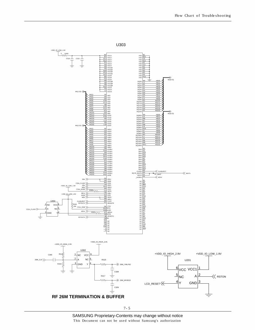
9. Memory(U303)
This system uses Samsung's memory, KAP17SG00A. The KAP17SG00A is a Multi Chip Package Memory which
combines 256Mbit Synchronous Burst Multi Bank NOR Flash Memory and two 512Mbit OneNAND Flash and
128Mbit Synchronous Burst UtRAM.
It has 16 bit data line, HD[1~16] which is connected to PCF5213EL1 and MV3018SAQ, also has 24 bit address lines,
HA[1~24]. There are 3 chip select signals, CS0n_FLASH, CS4n_NAND, and CS1n_RAM.
In the Writing process, WEn is fallen to low and it enables writing process to operate. During reading process,
OEn is fallen to low and it enables reading process to operate. Each chip select signals in the PCF5213EL1 choose
different memories.

SAMSUNG Proprietary-Contents may change without noticeThis Document can not be used without Samsung's authorization
Circuit Description
2-4
10. PCF5213EL1(U200)
The PCF5213EL1 is mainly composed of embeded DSP and ARM core. The DSP subsystem includes the Saturn
DSP core with embedded RAM and ROM, and a set of peripherals. It has 24kx16 bits PRAM, 104k*16 bits,
32k*16 XYRAM and 63k*16 XYROM in the DSP.
The ARM946E-S consists of an ARM9E-S processor core, 8 kbyte instruction cache and 8 kbyte data cache,
tghtly-coupled ITCM(Instruction Tightly Coupled Memory) and DTCM(Data Tightly Coupled Memory) memories, a
memory protection unit, and an AMBA(Advanced Microcontroller Bus Architecture) AHB(Advanced
High-performance Bus) bus interface with a write buffer.
HD(0:15), data lines and HA(0:23), address lines are connected to KAP17SG00A (memory), MV3018B (image dsp)
and YMU762 (melody IC). It has 64 kbyte SC RAM (0.5 Mbit) and 32 kbyte SC program ROM for bootstrap
loader in the ARM core.
HD(0:15), data lines and HA(0:23), address lines are connected to memory and YMU762 to communicate.
MV3018B(Camera DSP Chip) controls the communication between ARM core and DSP core.
OEn, WEn control the access of memory. KROW, and KCOL recognize the key string input status.
It has J-TAG control pins (TDI/TDO/TCK) for ARM and DSP core. J-SEL signal controls different access to ARM
and DSP core.
ADC(Analog to Digital Convertor) receives the condition of temperature, battery type and battery voltage.
11. TCO-5871U(26MHz)(U102)
This system uses the 26MHz TCXO, TCO-5871U, Toyocom. AFC control signal form PCF5213EL1 controls
frequency from 26MHz x-tal. It generates the clock frequency. This clock is connected to PCF5213EL1, YMU762 and
HD155166.
12. Camera DSP(MV3018SAQ)(U305)
MV3018SAQ provides rich video functions up to 30-frame display with minimized tasks in the handset main processor
as well as hardware based real-time JPEG compression and decompression. MV3018SAQ directly transmits and
previews the RGB data to the LCD graphic memory by processing the sensor output data according to the
handset's command. It can save the raw RGB data up to VGA resoultion into its image buffer and allows the
host processor to download with scalable sized compressed data.
It utilizes 16 bit data bus for communication with the main processor, including bus interface types.

SAMSUNG Proprietary-Contents may change without notice
3. SGH-E350 Exploded View and its Parts list
3-1
This Document can not be used without Samsung's authorization
1. Exploded View
QFU01
QKP02
QMP02
QFL01
QCR05
QSC01
QSP01
QMO01
QME02
QLC01
QVK01
QAN02
QRF01
QRF03
QVO01
QCW01
QFR01
QKP01
QMP01
QRE01
QCK01
QCA01
QIF01
QCR06
QBA01
QMI01
QCA02
QME01
QPC01

SAMSUNG Proprietary-Contents may change without notice
Exploded view and its Part list
3-2
This Document can not be used without Samsung's authorization
2. Parts list
Location NO. Description SEC CODE
QAN02 INTENNA-SGHE350;EWPADF013A,SGH-E350, GH42-00592A
QBA01 BATTERY-800MAH,B SIL,ORA,M;BST4208SO GH43-01920C
QCA01 UNIT-CAMERA;SGH-E350,MOMBH150G1A,-,E GH59-02179A
QCA02 UNIT-CAMERA KEY;SGH-E350,SGH-E350 C/ GH59-02183A
QCR05 SCREW-MACHINE;PH,+,M1.4,L3,ZPC(BLK), 6001-001478
QCR06 SCREW-MACHINE;PH(PI2.5),+,M1.4,L3.5, 6001-001155
QCW01 MEC-CAMERA WINDOW;SGH-E350,EU,-,-,-, GH75-07339A
QFL01 MEC-SLIDE LOWER;SGH-E350,EU,-,-,-,-, GH75-07260A
QFR01 MEC-FRONT COVER;SGH-E350,EU,-,-,-,-, GH75-07261A
QFU01 MEC-SLIDE UPPER;SGH-E350,EU,-,-,-,-, GH75-07259A
QIF01 PMO-IF COVER;SGH-E350,PC(G6656)+URET GH72-20661A
QKP01 MEC-KEYPAD MAIN;SGH-E350,EU,-,-,-,-, GH75-07285A
QKP02 MEC-KEYPAD SUB;SGH-E350,EU,-,-,-,-,B GH75-07284A
QLC01 LCD-SGHE350;LTS166QQ-F02,SGH-E350,12 GH07-00729A
QME01 UNIT-METAL DOME(MAIN);SGH-E350,SGH-E GH59-02182A
QME02 UNIT-METAL DOME(SUB);SGH-E350,SGH-E3 GH59-02181A
QMI01 MICROPHONE-ASSY-SGHE350;1,130to500uA GH30-00203A
QMO01 MOTOR DC-SGHE350;JHV-10A1-F13,SGH-E3 GH31-00176A
QMP01 PBA MAIN-SGHE350EDGE;SCH-E350,TINY,E GH92-02179A
QMP02 PBA SUB-SGHE350;SGH-E350,TINY,EU,PBA GH92-02206A
QPC01 PCB-FPCB CABLE;SGH-E350,POLYIMIDE,3L GH41-00882A
QRE01 MEC-REAR COVER(FTM);SGH-E350E,FTM,-, GH75-07332A
QVO01 PMO-VOLUME KEY;SGH-E350,ABS+URETHAN, GH72-20665A
QCK01 PMO-CAMERA KEY;SGH-E350,ABS+URETHAN, GH72-20666A
QRF01 MPR-SHEET RF COVER;SGH-E350,PC SHEET GH74-16395A
QRF03 PMO-EAR COVER V2;SGH-E350,PC(G71770C GH72-22634A
QSC01 MPR-SLIDE/L SCREW SHEET;SGH-E350,PC GH74-16356A
QSP01 SPEAKER;0.7W,8ohmohm,122dB±2dB,850H 3001-001782
QVK01 UNIT-VOLUME KEY;SGH-E350,SGH-E350 V/ GH59-02180A

SAMSUNG Proprietary-Contents may change without notice
Exploded view and its Part list
3-3
This Document can not be used without Samsung's authorization
Description SEC CODE
BAG PE;LDPE,T0.05,W80,L180,TRP,-,- 6902-000634
ADAPTOR-TAD;TAD137ESE,SGH-P100,-,110 GH44-00482A
UNIT-EARPHONE;SGH-Z107,EM-SS650E-ST, GH59-01713A
LABEL(P)-WATER SOAK;COMM,NORGE,100G, GH68-02026A
MANUAL-WEEE CARD;COMM,SEC,ENGLISH,UN GH68-07013A
LABEL(R)-MAIN(EU);SGH-E350,EU,POLYES GH68-07204A
MANUAL-USER;SGH-E350E,FTM,FRENCH,FRA GH68-07302A
MANUAL-QSG;SGH-E350E,FTA,FRENCH,FRAN GH68-07320A
CUSHION-CASE(1-2);SGH-E350,PULP,T0.8 GH69-03012A
BOX(P)-UINIT(ORANGE);SGH-E350,SC300+ GH69-03026A
PMO-BATT LOCKER;SGH-E350,PC(G6656),S GH72-20662A
RMO-RUBBER BGA 1;SGH-E350,CR RUBBER, GH73-05089A
RMO-RUBBER BGA 2;SGH-E350,CR RUBBER, GH73-05090A
RMO-RUBBER BGA 3;SGH-E350,CR RUBBER, GH73-05091A
MPR-TAPE SUB FPCB;SGH-E350,3M 851,28 GH74-16170A
MPR-TAPE LCD FPCB CONN;SGH-E350,3M 8 GH74-16171A
MPR-TAPE MAIN FPCB BASE;SGH-E350,PET GH74-16218A
MPR-TAPE MAIN FPCB;SGH-E350,3M 851,2 GH74-16219A
MPR-BOHO VINYL U/WIN;SGH-E350,3M 418 GH74-16358A
MPR-BOHO VINYL SUB KEY;SGH-E350,3M 4 GH74-16359A
MPR-TAPE EMI LCD R;SGH-E350,EMI TPAE GH74-16368A
MPR-TAPE EMI LCD L;SGH-E350,EMI TPAE GH74-16369A
MPR-TAPE EMI MAIN PCB;SGH-E350,EMI T GH74-16370A
MPR-TAPE EMI SUB PCB TOP;SGH-E350,EM GH74-16371A
MPR-TAPE SUB PCB BOT;SGH-E350,3M 851 GH74-16373A
MPR-TAPE MAIN PCB A;SGH-E350,3M 851, GH74-16787A
MEC-HANGER;SGH-Z500,TMN,STRAP,-,BLK, GH75-03673H

SAMSUNG Proprietary-Contents may change without notice
Exploded view and its Part list
3-4
This Document can not be used without Samsung's authorization
3. Test Jig (GH80-03306A)
3-2. RF Test Cable
(GH39-00283A)
3-3. Test Cable
(GH39-00337A)
3-5. Power Supply Cable 3-6. DATA CABLE
(GH39-00331A]
3-7. TA
(GH44-00482A)
3-1. USB JIG Cable
3-4. Serial Cable
(CSA LL64151-A)

SAMSUNG Proprietary-Contents may change without notice
4. Electrical Parts List
4-1
This Document can not be used without Samsung's authorization
SEC CODE Description Design LOC
0403-001387 ZD500 DIODE-ZENER
0403-001427 ZD501 DIODE-ZENER
0404-001172 D400 DIODE-SCHOTTKY
0404-001172 D401 DIODE-SCHOTTKY
0406-001208 ZD601 DIODE-TVS
0406-001208 ZD700 DIODE-TVS
0406-001208 ZD701 DIODE-TVS
0406-001208 ZD702 DIODE-TVS
0406-001208 ZD703 DIODE-TVS
0504-001151 U202 TR-DIGITAL
0504-001151 U203 TR-DIGITAL
0504-001151 U204 TR-DIGITAL
0504-001151 U502 TR-DIGITAL
0601-001754 LED600 LED
0601-001754 LED601 LED
0601-001754 LED602 LED
0601-001754 LED603 LED
0601-001754 LED604 LED
0601-001754 LED605 LED
0601-001754 LED606 LED
0601-001754 LED607 LED
0604-001291 U301 PHOTO-IRDA
0801-002958 U302 IC-CMOS LOGIC
0801-002970 U703 IC-CMOS LOGIC
1009-001020 U607 IC-HALL EFFECT S/W
1201-002223 U101 IC-POWER AMP
1202-001068 U600 IC-VOLTAGE COMP
1203-003321 U700 IC-DC/DC CONVERTER
1203-003340 U401 IC-POSI.FIXED REG
1203-003340 U606 IC-POSI.FIXED REG
1203-003432 U701 IC-POSI.FIXED REG
1203-003545 U402 IC-DC/DC CONVERTER
1203-003568 U400 IC-POWER SUPERVISOR
1203-003742 U501 IC-BATTERY
1204-002161 U300 IC-MELODY
1205-002636 U200 IC-COMM. CONTROLLER

SAMSUNG Proprietary-Contents may change without notice
Electrical Parts List
4-2
This Document can not be used without Samsung's authorization
SEC CODE Description Design LOC
1205-002709 U100 IC-TRANSCEIVER
1404-001221 V500 THERMISTOR-NTC
1405-001082 V400 VARISTOR
1405-001082 V601 VARISTOR
1405-001082 V602 VARISTOR
1405-001082 V700 VARISTOR
1405-001082 V701 VARISTOR
1405-001082 V702 VARISTOR
1405-001082 V703 VARISTOR
1405-001082 V704 VARISTOR
1405-001082 V705 VARISTOR
1405-001082 V706 VARISTOR
1405-001110 V603 VARISTOR
1405-001110 V604 VARISTOR
1405-001110 V707 VARISTOR
1405-001110 V708 VARISTOR
1405-001110 V709 VARISTOR
1405-001110 V710 VARISTOR
1405-001110 V711 VARISTOR
1405-001110 V712 VARISTOR
2007-000070 R303 R-CHIP
2007-000137 R507 R-CHIP
2007-000137 R600 R-CHIP
2007-000137 R602 R-CHIP
2007-000138 R115 R-CHIP
2007-000138 R517 R-CHIP
2007-000138 R518 R-CHIP
2007-000138 R701 R-CHIP
2007-000138 R702 R-CHIP
2007-000138 R703 R-CHIP
2007-000138 R704 R-CHIP
2007-000138 R705 R-CHIP
2007-000143 R104 R-CHIP
2007-000143 R105 R-CHIP
2007-000143 R108 R-CHIP
2007-000143 R109 R-CHIP

SAMSUNG Proprietary-Contents may change without notice
Electrical Parts List
4-3
This Document can not be used without Samsung's authorization
SEC CODE Description Design LOC
2007-000143 R216 R-CHIP
2007-000143 R307 R-CHIP
2007-000143 R308 R-CHIP
2007-000148 R101 R-CHIP
2007-000148 R200 R-CHIP
2007-000148 R218 R-CHIP
2007-000148 R302 R-CHIP
2007-000148 R309 R-CHIP
2007-000148 R313 R-CHIP
2007-000148 R504 R-CHIP
2007-000151 R305 R-CHIP
2007-000152 R519 R-CHIP
2007-000156 R511 R-CHIP
2007-000162 R201 R-CHIP
2007-000162 R207 R-CHIP
2007-000162 R211 R-CHIP
2007-000162 R212 R-CHIP
2007-000162 R213 R-CHIP
2007-000162 R214 R-CHIP
2007-000162 R215 R-CHIP
2007-000162 R306 R-CHIP
2007-000162 R311 R-CHIP
2007-000162 R401 R-CHIP
2007-000162 R405 R-CHIP
2007-000162 R501 R-CHIP
2007-000162 R503 R-CHIP
2007-000162 R509 R-CHIP
2007-000162 R605 R-CHIP
2007-000162 R607 R-CHIP
2007-000162 R608 R-CHIP
2007-000162 R609 R-CHIP
2007-000162 R617 R-CHIP
2007-000162 R707 R-CHIP
2007-000162 R708 R-CHIP
2007-000170 R203 R-CHIP
2007-000170 R204 R-CHIP

SAMSUNG Proprietary-Contents may change without notice
Electrical Parts List
4-4
This Document can not be used without Samsung's authorization
SEC CODE Description Design LOC
2007-000170 R205 R-CHIP
2007-000170 R206 R-CHIP
2007-000170 R513 R-CHIP
2007-000170 R514 R-CHIP
2007-000171 C100 R-CHIP
2007-000171 R100 R-CHIP
2007-000171 R102 R-CHIP
2007-000171 R106 R-CHIP
2007-000171 R110 R-CHIP
2007-000171 R112 R-CHIP
2007-000171 R113 R-CHIP
2007-000171 R114 R-CHIP
2007-000171 R116 R-CHIP
2007-000171 R117 R-CHIP
2007-000171 R118 R-CHIP
2007-000171 R120 R-CHIP
2007-000171 R202 R-CHIP
2007-000171 R300 R-CHIP
2007-000171 R310 R-CHIP
2007-000171 R319 R-CHIP
2007-000171 R403 R-CHIP
2007-000171 R404 R-CHIP
2007-000171 R406 R-CHIP
2007-000171 R407 R-CHIP
2007-000171 R515 R-CHIP
2007-000171 R516 R-CHIP
2007-000171 R520 R-CHIP
2007-000172 R103 R-CHIP
2007-000172 R107 R-CHIP
2007-000242 R209 R-CHIP
2007-000242 R210 R-CHIP
2007-000758 R500 R-CHIP
2007-000758 R502 R-CHIP
2007-000831 R304 R-CHIP
2007-000831 R604 R-CHIP
2007-000839 R312 R-CHIP

SAMSUNG Proprietary-Contents may change without notice
Electrical Parts List
4-5
This Document can not be used without Samsung's authorization
SEC CODE Description Design LOC
2007-001303 R315 R-CHIP
2007-001303 R317 R-CHIP
2007-001316 R408 R-CHIP
2007-001316 R603 R-CHIP
2007-001325 R301 R-CHIP
2007-007001 R208 R-CHIP
2007-007009 R611 R-CHIP
2007-007009 R612 R-CHIP
2007-007009 R613 R-CHIP
2007-007009 R614 R-CHIP
2007-007009 R615 R-CHIP
2007-007009 R616 R-CHIP
2007-007009 R618 R-CHIP
2007-007009 R619 R-CHIP
2007-007013 R706 R-CHIP
2007-007014 R314 R-CHIP
2007-007014 R316 R-CHIP
2007-007100 U704 R-CHIP
2007-007310 R700 R-CHIP
2007-007334 R510 R-CHIP
2007-007480 R610 R-CHIP
2007-007489 R512 R-CHIP
2007-007573 R508 R-CHIP
2007-007573 R606 R-CHIP
2203-000233 C122 C-CER,CHIP
2203-000233 C139 C-CER,CHIP
2203-000233 C300 C-CER,CHIP
2203-000233 C409 C-CER,CHIP
2203-000233 C704 C-CER,CHIP
2203-000254 C128 C-CER,CHIP
2203-000254 C131 C-CER,CHIP
2203-000254 C133 C-CER,CHIP
2203-000254 C141 C-CER,CHIP
2203-000254 C200 C-CER,CHIP
2203-000254 C205 C-CER,CHIP
2203-000254 C207 C-CER,CHIP

SAMSUNG Proprietary-Contents may change without notice
Electrical Parts List
4-6
This Document can not be used without Samsung's authorization
SEC CODE Description Design LOC
2203-000254 C405 C-CER,CHIP
2203-000254 C412 C-CER,CHIP
2203-000254 C617 C-CER,CHIP
2203-000254 C713 C-CER,CHIP
2203-000278 C115 C-CER,CHIP
2203-000278 C116 C-CER,CHIP
2203-000278 C117 C-CER,CHIP
2203-000278 C600 C-CER,CHIP
2203-000278 C611 C-CER,CHIP
2203-000278 C614 C-CER,CHIP
2203-000278 C619 C-CER,CHIP
2203-000278 C626 C-CER,CHIP
2203-000311 C506 C-CER,CHIP
2203-000438 C138 C-CER,CHIP
2203-000438 C140 C-CER,CHIP
2203-000438 C304 C-CER,CHIP
2203-000438 C318 C-CER,CHIP
2203-000438 C321 C-CER,CHIP
2203-000438 C627 C-CER,CHIP
2203-000585 C123 C-CER,CHIP
2203-000628 C127 C-CER,CHIP
2203-000628 C130 C-CER,CHIP
2203-000628 C132 C-CER,CHIP
2203-000628 C135 C-CER,CHIP
2203-000654 C120 C-CER,CHIP
2203-000654 C134 C-CER,CHIP
2203-000679 C301 C-CER,CHIP
2203-000679 C320 C-CER,CHIP
2203-000679 C325 C-CER,CHIP
2203-000679 C326 C-CER,CHIP
2203-000679 C327 C-CER,CHIP
2203-000725 C316 C-CER,CHIP
2203-000812 C102 C-CER,CHIP
2203-000812 C106 C-CER,CHIP
2203-000812 C203 C-CER,CHIP
2203-000812 C210 C-CER,CHIP

SAMSUNG Proprietary-Contents may change without notice
Electrical Parts List
4-7
This Document can not be used without Samsung's authorization
SEC CODE Description Design LOC
2203-000812 C215 C-CER,CHIP
2203-000812 C218 C-CER,CHIP
2203-000812 C219 C-CER,CHIP
2203-000812 C220 C-CER,CHIP
2203-000812 C700 C-CER,CHIP
2203-000812 C701 C-CER,CHIP
2203-000995 C107 C-CER,CHIP
2203-001259 C105 C-CER,CHIP
2203-001259 C114 C-CER,CHIP
2203-002443 C612 C-CER,CHIP
2203-002525 C313 C-CER,CHIP
2203-002668 C103 C-CER,CHIP
2203-002668 C113 C-CER,CHIP
2203-002668 C118 C-CER,CHIP
2203-003054 C407 C-CER,CHIP
2203-003054 C410 C-CER,CHIP
2203-003054 C621 C-CER,CHIP
2203-003054 C628 C-CER,CHIP
2203-003054 C629 C-CER,CHIP
2203-005056 C606 C-CER,CHIP
2203-005056 C616 C-CER,CHIP
2203-005288 C104 C-CER,CHIP
2203-005288 C119 C-CER,CHIP
2203-005288 C121 C-CER,CHIP
2203-005480 C315 C-CER,CHIP
2203-005480 C402 C-CER,CHIP
2203-005482 C136 C-CER,CHIP
2203-005482 C137 C-CER,CHIP
2203-005482 C201 C-CER,CHIP
2203-005482 C202 C-CER,CHIP
2203-005482 C204 C-CER,CHIP
2203-005482 C206 C-CER,CHIP
2203-005482 C208 C-CER,CHIP
2203-005482 C211 C-CER,CHIP
2203-005482 C217 C-CER,CHIP
2203-005482 C302 C-CER,CHIP

SAMSUNG Proprietary-Contents may change without notice
Electrical Parts List
4-8
This Document can not be used without Samsung's authorization
SEC CODE Description Design LOC
2203-005482 C305 C-CER,CHIP
2203-005482 C307 C-CER,CHIP
2203-005482 C308 C-CER,CHIP
2203-005482 C309 C-CER,CHIP
2203-005482 C312 C-CER,CHIP
2203-005482 C314 C-CER,CHIP
2203-005482 C317 C-CER,CHIP
2203-005482 C323 C-CER,CHIP
2203-005482 C406 C-CER,CHIP
2203-005482 C419 C-CER,CHIP
2203-005482 C501 C-CER,CHIP
2203-005482 C503 C-CER,CHIP
2203-005482 C504 C-CER,CHIP
2203-005482 C603 C-CER,CHIP
2203-005482 C604 C-CER,CHIP
2203-005482 C609 C-CER,CHIP
2203-005482 C613 C-CER,CHIP
2203-005482 C624 C-CER,CHIP
2203-005482 C625 C-CER,CHIP
2203-005482 C703 C-CER,CHIP
2203-005482 C706 C-CER,CHIP
2203-005482 C712 C-CER,CHIP
2203-005482 C715 C-CER,CHIP
2203-005482 C716 C-CER,CHIP
2203-005482 C719 C-CER,CHIP
2203-005496 C110 C-CER,CHIP
2203-005512 C311 C-CER,CHIP
2203-006053 C212 C-CER,CHIP
2203-006053 C213 C-CER,CHIP
2203-006053 C214 C-CER,CHIP
2203-006053 C310 C-CER,CHIP
2203-006053 C505 C-CER,CHIP
2203-006053 R324 C-CER,CHIP
2203-006091 C631 C-CER,CHIP
2203-006093 C414 C-CER,CHIP
2203-006137 C623 C-CER,CHIP

SAMSUNG Proprietary-Contents may change without notice
Electrical Parts List
4-9
This Document can not be used without Samsung's authorization
SEC CODE Description Design LOC
2203-006190 C630 C-CER,CHIP
2203-006201 C710 C-CER,CHIP
2203-006201 C711 C-CER,CHIP
2203-006208 C209 C-CER,CHIP
2203-006208 C418 C-CER,CHIP
2203-006208 C423 C-CER,CHIP
2203-006208 C426 C-CER,CHIP
2203-006208 C705 C-CER,CHIP
2203-006257 C306 C-CER,CHIP
2203-006257 C319 C-CER,CHIP
2203-006257 C322 C-CER,CHIP
2203-006257 C400 C-CER,CHIP
2203-006257 C403 C-CER,CHIP
2203-006257 C408 C-CER,CHIP
2203-006257 C416 C-CER,CHIP
2203-006257 C417 C-CER,CHIP
2203-006257 C424 C-CER,CHIP
2203-006257 C620 C-CER,CHIP
2203-006257 C622 C-CER,CHIP
2203-006257 C708 C-CER,CHIP
2203-006257 C709 C-CER,CHIP
2203-006257 C717 C-CER,CHIP
2203-006257 C718 C-CER,CHIP
2203-006257 C720 C-CER,CHIP
2404-001225 C303 C-TA,CHIP
2404-001225 C404 C-TA,CHIP
2404-001225 C413 C-TA,CHIP
2404-001225 C415 C-TA,CHIP
2404-001225 C425 C-TA,CHIP
2404-001268 C502 C-TA,CHIP
2404-001348 C108 C-TA,CHIP
2404-001352 C401 C-TA,CHIP
2404-001352 C411 C-TA,CHIP
2404-001374 C109 C-TA,CHIP
2404-001374 C126 C-TA,CHIP
2404-001374 C129 C-TA,CHIP

SAMSUNG Proprietary-Contents may change without notice
Electrical Parts List
4-10
This Document can not be used without Samsung's authorization
SEC CODE Description Design LOC
2703-001723 R402 INDUCTOR-SMD
2703-002155 L101 INDUCTOR-SMD
2703-002313 L200 INDUCTOR-SMD
2703-002313 L201 INDUCTOR-SMD
2703-002313 L202 INDUCTOR-SMD
2703-002365 L102 INDUCTOR-SMD
2703-002365 L103 INDUCTOR-SMD
2703-002365 L107 INDUCTOR-SMD
2703-002365 L108 INDUCTOR-SMD
2703-002586 L100 INDUCTOR-SMD
2703-002596 L105 INDUCTOR-SMD
2801-004339 OSC400 CRYSTAL-SMD
2809-001294 U102 OSCILLATOR-VCTCXO
2901-001283 F500 FILTER-EMI SMD
2901-001319 F700 FILTER-EMI SMD
2901-001319 F701 FILTER-EMI SMD
2901-001319 F702 FILTER-EMI SMD
2901-001319 F703 FILTER-EMI SMD
2901-001319 F704 FILTER-EMI SMD
2901-001319 F705 FILTER-EMI SMD
2901-001319 F706 FILTER-EMI SMD
2901-001322 F501 FILTER-EMI SMD
2901-001322 F502 FILTER-EMI SMD
3301-001120 L400 BEAD-SMD
3301-001534 L600 BEAD-SMD
3301-001729 L700 BEAD-SMD
3301-001729 L701 BEAD-SMD
3705-001355 CN100 CONNECTOR-COAXIAL
3708-001966 CN700 CONNECTOR-FPC/FFC/PIC
3709-001355 SIM400 CONNECTOR-CARD EDGE
3710-001611 IFC500 CONNECTOR-INTERFACE
3711-005801 CN701 CONNECTOR-HEADER
3711-005829 BTC500 CONNECTOR-BATTERY
4302-001177 BAT400 BATTERY-LI(2ND)
GH13-00029A U305 IC ASIC-SCHN480

SAMSUNG Proprietary-Contents may change without noticeThis Document can not be used without Samsung's authorization
5. SGH-E350 Block Diagrams
5-1
1. RF Solution Block Diagram

SAMSUNG Proprietary-Contents may change without notice
Block Diagrams
This Document can not be used without Samsung's authorization
5-2
2. Base Band Solution Block Diagram

SAMSUNG Proprietary-Contents may change without notice
6. SGH-E350 PCB Diagrams
6-1
This Document can not be used without Samsung's authorization
1. MAIN PCB Top Diagram

SAMSUNG Proprietary-Contents may change without notice
PCB Diagrams
6-2
This Document can not be used without Samsung's authorization
2. MAIN PCB Bottom Diagram

SAMSUNG Proprietary-Contents may change without notice
PCB Diagrams
2-3
This Document can not be used without Samsung's authorization
3. SUB Top Diagram

SAMSUNG Proprietary-Contents may change without notice
PCB Diagrams
6-4
This Document can not be used without Samsung's authorization
4. SUB Bottom Diagram

SAMSUNG Proprietary-Contents may change without notice
7. SGH-E350 Flow Chart of Troubleshooting
This Document can not be used without Samsung's authorization
7-1
1. Power On
Check the Battery Voltage
is more than 3.4V
' Power On ' does not work
Change the Battery
END
No
Yes
C408(VINT) = 2.7V? Check the PMU related to VINTNo
Yes
Check the Clock at
U704=32KHZResolder OSC400
No
Yes
C424(+VDD_IO_LOW) &C423(+VDD_IO_HIGH) = "H"? Check the related circuit
No
Yes
C402(+VDD_GSM_CORE)
= 1.8V?
Check the +VDD_GSM_CORE circuitNo
Yes
Check for the clock at C300
= 26MHz
Check the clock generation circuit
(related to U100)
No
Yes
Check the initial operation
Yes
Yes

SAMSUNG Proprietary-Contents may change without noticeThis Document can not be used without Samsung's authorization
Flow Chart of Troubleshooting
7-2
SIM
_VC
C
VD
D_IO
_HIG
H
2.9V
not use
DC
DC
- 1.875V
AV
DD
_HF
A
1.9V
VC
C_R
X_T
X
VD
D_IM
AG
E
VD
D_IO
_LO
W
VC
C_S
YN
VD
D_G
SM
_CO
RE
VD
D_4V
2.7V
MIC
_BIA
S
SIM
_CLK
2.7V
2.6V
VD
D_V
IB_2.9
AV
DD
SIM
_IO
VD
D_S
LE
EP
2.9V
3.3V LD
O
VD
D_V
IB
2.1V
SIM
_RS
T
2.6V
2.9V
BT
_NO
T_U
SE
no
t use
2.9V
C411
C414
C417
C422
3 4 5 6
G 7
8 G
G
9 10 G
SIM
400
1 2
C423
R402
R405
C416
V400
R404
BA
T400
C426
T400
C415
C418
27
_ONKEY
1
_REC1
13 _RE
C2
11
_RSTHC
44 _S
IMR
SC
D
7
_SIMRSHC
SIM
IOC
D
9
SIMIOHC
41 S
IMV
CC
31
VBAT
32
VCHG
29
VINT
30
VSAVE
10
_IRQ
2
SCL
38 S
CN
37 S
CP
3
SDA
43 S
IMC
KC
D
8
SIMCKHC
40 S
IMD
3VB
AT 45
SIM
EN
42
OSCI 25
OSCO
6
PWREN1
5
PWREN2
28
REFC
23 RF
12VB
AT
RF
1VD
D
22
24 RF
2VD
D
17 HC
VD
D
15 IOD
2VB
AT
IOV
DD
14 LP
D1V
BA
T 20
19 LPV
DD
12
MICBIAS
53 N
C
NC
54
26
49 G
ND
G
ND
50 51
GN
D
GN
D 52
48 G
PO
1 47 G
PO
2 46 G
PO
3
HC
VB
AT
18
CHGCUR/BATMAX 33
CHGDRV
4
CLK32K
36
CPVBAT 35
CPVDD
21 D1V
DD
D2V
DD
16
39 D
3VD
D
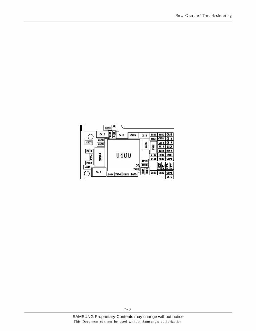
U400
34
OS
C400
R407
C420
C424
C421
R403
+VD
D_IO
_LOW
_2.9V
R408
C407
C410
C406
C419
R406
C408
C413
C409
U704
C425
C412
BA
CK
LIGH
T
+VC
C_S
YN
_2.8V
+VD
D_S
LEE
P_2.9V
+AV
DD
_HF
A_2.6V
+AV
DD
_2.6V
+VD
D_IM
AG
E_2.9V
VB
AT
BU
_RS
T
IT_P
MU
ON
KE
YN
AU
X_O
N
RS
TO
N
SIM
RS
T
32KH
z_DIG
IT
RE
F_O
N
PO
N_T
X
SC
L SD
A
SIM
CLK
SIM
IO
+VD
D_R
X_T
X_2.8V
+VD
D_IO
_HIG
H_2.9V
+VD
D_IO
_LOW
_1.9V
MIC
_BIA
S
SAMSUNG Proprietary-Contents may change without notice
Flow Chart of Troubleshooting
This Document can not be used without Samsung's authorization
7-3

SAMSUNG Proprietary-Contents may change without noticeThis Document can not be used without Samsung's authorization
Flow Chart of Troubleshooting
7-4
2. Initial
U201 pin 2 (RSTON) ="H"?
Initial Failure
Check the circuit related to reset
END
No
Yes
Is U304 pin 4
OK?
Yes
Yes
NoCheck the U304
Check the 16bit data signal& memory CE
Yes
SAMSUNG Proprietary-Contents may change without notice
Flow Chart of Troubleshooting
This Document can not be used without Samsung's authorization
7-5
TP_WAIT
A 2
GND 3
1 NC
NC 5
VCC 6
4 Y
U304
C318
+VDD_IO_LOW_1.9V
+VDD_IO_LOW_1.9V
R306
C319
N4 /OER
P3 /OEU
/RESETR D7
C6 /UBU
H11 /WEO
B8 /WER
B9 /WEU
/WPR C1
_AVDRU F6
G6 _CSU
_MRSU E7
J9 _RESETO
E4 /CEO
M4 /CER
C7 /LBU
L4 /OEO
B10 VSS VSS
C8
VSS E12
VSS F2 J12 VSS
VSS K2 M2
VSS VSS N2
VCCU N11 P7
VCCU VCCU N3
C5 VPPR
VSS B2
P4 VSS VSS
P8 P10 VSS
VCCQU N10 P11
VCCQU VCCR
N12 B5 VCCR
VCCR N1
B3 VCCU VCCU
B7 B11
VCCU
G12 VCCO VCCO
F3 L2
VCCO
VCCQR N5 N6 VCCQR
VCCQR N9
VCCQU P5 P6
VCCQU
NC 1 2
NC
C12 NC NC D1
NC E1
NC F1
F5 RDYO
D5 RDYR_WAITU
M1 NC NC M12
B12 NC
N8 NC
NC P1 P2 NC
NC P9
P12 NC
H7 NC NC J1
J2 NC NC J6
K12 NC NC
K1 L1 NC
NC L12
NC F12 G1
NC G2 NC H1
NC NC
H2 H12 NC
NC H6
B6 NC
M10 DQ7RU
DQ8O K4
J7 DQ8RU
L3 DQ9O
J8 DQ9RU
G11 INTO
NC B1
F7 NC
N7 DQ3RU
DQ4O J3
K7 DQ4RU
H4 DQ5O
M8 DQ5RU
DQ6O G3
DQ6RU L9
G5 DQ7O
DQ14RU M9
F4 DQ15O
M11 DQ15RU
L5 DQ1O
L6 DQ1RU
DQ2O K5
DQ2RU M6
J4 DQ3O
DQ10RU M7
J5 DQ11O
L7 DQ11RU
DQ12O H3
DQ12RU L8
H5 DQ13O
H8 DQ13RU
DQ14O G4
DNU A12 R1 DNU R2
DNU R3 DNU
DNU R10
DQ0O M3
DQ0RU M5
DQ10O K3
E5 CLKO
E6 CLKRU
A2 DNU
R11 DNU DNU R12
A3 DNU DNU A10
A11 DNU
E3 A6RU
F11 A7O
C4 A7RU
A8O J11
F8 A8RU
J10 A9O
A9RU C9
H10 AVDO
D2 A2RU
F10 A3O
E2 A3RU
A4O E11
C3 A4RU
H9 A5O
A5RU D3
A6O G10
A19RU E8
G8 A1O
C2 A1RU
D8 A20RU A21RU
D6 C11 A22RU
A23R D12
A2O G9
A13RU E10
A14O K8
D11 A14RU
L10 A15O
A15RU C10 G7
A16RU A17RU B4
D4 A18RU
K6 A0RU
A10O K11
D9 A10RU
K10 A11O
A11RU D10
A12O K9
E9 A12RU
L11 A13O
U303
A0O F9
10K R309
+VDD_IO_LOW_1.9V
0 R300
R310
RSTEXTn
HA(2)
HA(1:24)
HD(15) HD(14) HD(13) HD(12) HD(11) HD(10)
HD(9) HD(8) HD(7) HD(6) HD(5) HD(4) HD(3) HD(2) HD(1)
HD(0:15) HD(0)
HA(0)
HA(1)
HA(18) HA(17) HA(16) HA(15) HA(14) HA(13) HA(12) HA(11) HA(10) HA(9) HA(8) HA(7) HA(6) HA(5) HA(4) HA(3)
ADVn
CS4n_NAND
CS1n_RAM
RSTEXTn
CS0n_FLASH
OEn
BE1n
HA(23) HA(22) HA(21) HA(20) HA(19)
HD(10) HD(9) HD(8) HD(7) HD(6) HD(5) HD(4) HD(3) HD(2) HD(1)
HD(0:15) HD(0)
WEn
CLKBURST
HA(24) WAITn
WEn
CLKBURST
HA(12) HA(11) HA(10) HA(9) HA(8) HA(7) HA(6) HA(5) HA(4) HA(3) HA(2)
HA(1:16)
HA(1)
ADVn
OEn
HD(15) HD(14) HD(13) HD(12) HD(11)
CS2n_FLASH
HA(16) HA(15) HA(14) HA(13)
RF 26M TERMINATION & BUFFER
R314
R315
R316
R317
C300
+VDD_IO_HIGH_2.9V
NC 5
6 VCC
4 Y
U302
A 2
3 GND
1 NC
C329
C328
+VDD_IO_HIGH_2.9V
26M_YMU762
26M_MV3018
26M_CLK
+VDD_IO_HIGH_2.9V
NC 5
6 VCC VCC1 1
Y 4
U201
2 A
3 GND
+VDD_IO_LOW_1.9V
RSTON
LCD_RESET

SAMSUNG Proprietary-Contents may change without noticeThis Document can not be used without Samsung's authorization
Flow Chart of Troubleshooting
7-6
SAMSUNG Proprietary-Contents may change without notice
Flow Chart of Troubleshooting
This Document can not be used without Samsung's authorization
7-7
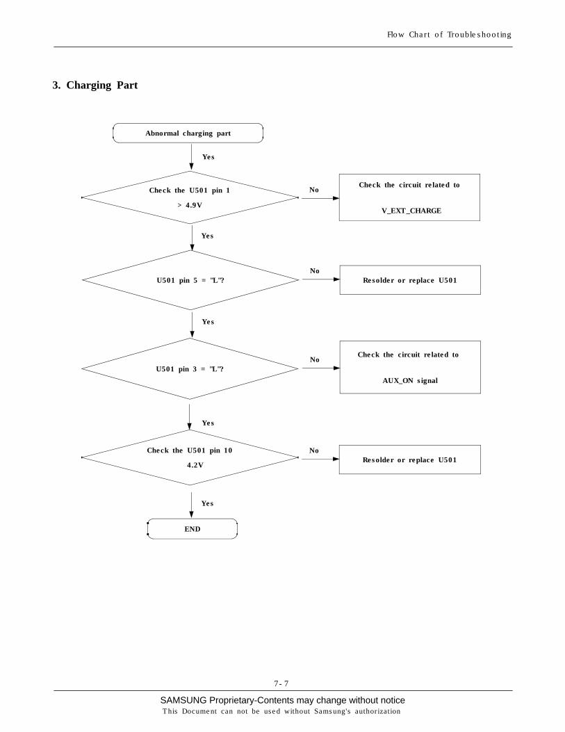
3. Charging Part
Check the U501 pin 1
> 4.9V
Abnormal charging part
END
No
Yes
U501 pin 5 = "L"?No
Yes
U501 pin 3 = "L"?No
Yes
Check the U501 pin 10
≒ 4.2V
No
Yes
Check the circuit related to
V_EXT_CHARGE
Resolder or replace U501
Check the circuit related to
AUX_ON signal
Resolder or replace U501
Yes

SAMSUNG Proprietary-Contents may change without noticeThis Document can not be used without Samsung's authorization
Flow Chart of Troubleshooting
7-8
BATTERY CHARGING
R507
R511 R512
R510 C501
C503
ZD500
R508
IMIN 6
2 USB
7 USBON 4 _CHG
_EN 5
_PPR 3
C502 U501
BAT 10 1
CRDL
GND 11
8 GND
ICDL 9
VBAT
C505
ZD501
+VDD_IO_HIGH_2.9V V_EXT_CHARGE
CHG_ON
END_OF_CHG
USB_CHG_ON
AUX_ON
+VBUS
MES_BATT

SAMSUNG Proprietary-Contents may change without notice
Flow Chart of Troubleshooting
This Document can not be used without Samsung's authorization
7-9
4. Sim Part
SIM400 pin 1,5 = "H"?
Phone can't access SIM Card
Check the sim charge pump
Check the SIM Card
END
No
Yes
Yes
Yes
No
Check the Clock
After Power ON,
Check SIMCLK Signal on
pin3 of SIM400 in a few second
Yes
No
Replace PBAAfter SIM card insert,
SIM400 pin 2 = "H(SIM_RST)"?
Yes

SAMSUNG Proprietary-Contents may change without noticeThis Document can not be used without Samsung's authorization
Flow Chart of Troubleshooting
7-10
SIM
_VC
C
VD
D_IO
_HIG
H
2.9V
not use
DC
DC
- 1.875V
AV
DD
_HF
A
1.9V
VC
C_R
X_T
X
VD
D_IM
AG
E
VD
D_IO
_LO
W
VC
C_S
YN
VD
D_G
SM
_CO
RE
VD
D_4V
2.7V
MIC
_BIA
S
SIM
_CLK
2.7V
2.6V
VD
D_V
IB_2.9
AV
DD
SIM
_IO
VD
D_S
LE
EP
2.9V
3.3V LD
O
VD
D_V
IB
2.1V
SIM
_RS
T
2.6V
2.9V
BT
_NO
T_U
SE
no
t use
2.9V
C411
C414
C417
C422
3 4 5 6
G 7
8 G
G
9 10 G
SIM
400
1 2
C423
R402
R405
C416
V400
R404
BA
T400
C426
T400
C415
C418
27
_ONKEY
1
_REC1
13 _RE
C2
11
_RSTHC
44 _S
IMR
SC
D
7
_SIMRSHC
SIM
IOC
D
9
SIMIOHC
41 S
IMV
CC
31
VBAT
32
VCHG
29
VINT
30
VSAVE
10
_IRQ
2
SCL
38 S
CN
37 S
CP
3
SDA
43 S
IMC
KC
D
8
SIMCKHC
40 S
IMD
3VB
AT 45
SIM
EN
42
OSCI 25
OSCO
6
PWREN1
5
PWREN2
28
REFC
23 RF
12VB
AT
RF
1VD
D
22
24 RF
2VD
D
17 HC
VD
D
15 IOD
2VB
AT
IOV
DD
14 LP
D1V
BA
T 20
19 LPV
DD
12
MICBIAS
53 N
C
NC
54
26
49 G
ND
G
ND
50 51
GN
D
GN
D 52
48 G
PO
1 47 G
PO
2 46 G
PO
3
HC
VB
AT
18
CHGCUR/BATMAX 33
CHGDRV
4
CLK32K
36
CPVBAT 35
CPVDD
21 D1V
DD
D2V
DD
16
39 D
3VD
D
U400
34
OS
C400
R407
C420
C424
C421
R403
+VD
D_IO
_LOW
_2.9V
R408
C407
C410
C406
C419
R406
C408
C413
C409
U704
C425
C412
BA
CK
LIGH
T
+VC
C_S
YN
_2.8V
+VD
D_S
LEE
P_2.9V
+AV
DD
_HF
A_2.6V
+AV
DD
_2.6V
+VD
D_IM
AG
E_2.9V
VB
AT
BU
_RS
T
IT_P
MU
ON
KE
YN
AU
X_O
N
RS
TO
N
SIM
RS
T
32KH
z_DIG
IT
RE
F_O
N
PO
N_T
X
SC
L SD
A
SIM
CLK
SIM
IO
+VD
D_R
X_T
X_2.8V
+VD
D_IO
_HIG
H_2.9V
+VD
D_IO
_LOW
_1.9V
MIC
_BIA
S

SAMSUNG Proprietary-Contents may change without notice
Flow Chart of Troubleshooting
This Document can not be used without Samsung's authorization
7-11

SAMSUNG Proprietary-Contents may change without noticeThis Document can not be used without Samsung's authorization
Flow Chart of Troubleshooting
7-12
5. Microphone Part
Check the connection
from MIC
Check the circuit
from U200 to MIC
Resolder MIC
Resolder the C603, C609, R600, R602
R603
END
No
Yes
Yes
Yes
Yes
No
Check U601 PIN 8= ' H' ?
NoCheck the JACK_EN signal
Microphone does not work
Yes
Check the MICNo
Replace the MIC

SAMSUNG Proprietary-Contents may change without notice
Flow Chart of Troubleshooting
This Document can not be used without Samsung's authorization
7-13
MICROPHONE
Close to MCP
C608
2
1
3
5
4
C606
U600
MIC_BIAS_BB
R605
C601
V601
C610
R610
+VDD_IO_HIGH_2.9V
C617
C602
C611
C605
R602
C600
MIC_BIAS
R603
C603
+VDD_IO_HIGH_2.9V
VCC
MIC MIC600 2
1B1 1S 8
2A 6 2B0
3
4 2B1
7 2S
5
GND
10 U601
9 1A 1B0
1
R604
R600
C607
R606
V602
C631
220NF
R601
C609
MIC_BIAS
MIC_CP
EAR_ADC
JACK_EN
EAR_SWITCH
MIC_N
MIC_P

SAMSUNG Proprietary-Contents may change without noticeThis Document can not be used without Samsung's authorization
Flow Chart of Troubleshooting
7-14
6. Speaker Part(Melody)
U302 pin 6 = 2.9V?
Speaker does not work
Check the Clock signal at
Pin 1 of U300 (26MHz)
Check the clock generation circuit
(related to U100and U300)
No
Yes
No
Resolder or replace U302
Yes
U300 pin 17,18 ≒ 1.8V?
(When U300 operate)Resolder U300
No
Yes
END
Is Speaker working? Change the Speaker
No
Yes
Yes
CN700 pin 23,25 ≒ 1.8V?
(When U300 operate)Resolder CN700
No
Yes

SAMSUNG Proprietary-Contents may change without notice
Flow Chart of Troubleshooting
This Document can not be used without Samsung's authorization
7-15
MELODY IC
CODEC
C316
C305
R305
TP_A1
C301
R304
R301 3.3K
C317
R302
C302
C315
C314
C311
9 VREF
8 VSS
/CS
29
3
/IRQ /R
D
31
/RST
4
28
/WR
19
MTR
5 NC
PLLC 6
17 SPOUT1
SPOUT2 18
15
SP
VD
D
SP
VS
S
16
7 VDD
34
G
G
35
36
G
HP
OU
T-L
/MO
NO
10 11
HP
OU
T-R
IOV
DD
32
LED 2 24
23 D4
D5 22
21 D6
D7 20
EQ
1
12 13
EQ
2
EQ
3
14
G
33
U300
30
A0
1 CLKI
D0
27 26
D1
25 D2
D3
C312 C310
+VDD_IO_HIGH_2.9V
C308
C304
C313
+VDD_IO_LOW_1.9V
EARP_HF
VCC_AUDIO_BAT
ANL
ANR
AMP_N
AMP_P
HD(1)
HD(0)
WEn
CS5n_MELODY
HA(1)
OEn
HD(2) 26M_YMU762
HD(3)
HD(4) M_INT
HD(5) RSTON
HD(6)
HD(7)
VIB
RF 26M TERMINATION & BUFFER
R314
R315
R316
R317
C300
+VDD_IO_HIGH_2.9V
NC 5
6 VCC
4 Y
U302
A 2
3 GND
1 NC
C329
C328
+VDD_IO_HIGH_2.9V
26M_YMU762
26M_MV3018
26M_CLK

SAMSUNG Proprietary-Contents may change without noticeThis Document can not be used without Samsung's authorization
Flow Chart of Troubleshooting
7-16
7. Key Data Input
When one of the keys is
pushed,
is it displayed on LCD?
Check the Dome sheet & Key Pad
END
No
Yes
Yes
Check Initial Operation
When one of the keys is
pushed,
KBIO signal is OK?
Replace the PBA
No
Yes

SAMSUNG Proprietary-Contents may change without notice
Flow Chart of Troubleshooting
This Document can not be used without Samsung's authorization
7-17
P.T.T
V_UP
V_DOWN
END_KEY
KEY_MAP
DIGIT6122
RIGHT12
DIGIT01
V70
8
V70
9
V71
2
SHARP112
SOFT112
DIGIT1
12
2
STAR1
12
DIGIT91
12
V71
0
DIGIT2
SOFT212
12SEND
12
V70
1
INT
V70
2
2DIGIT8
1
V71
1
END
12
12
DIGIT312
12
DIGIT7
2DOWN
DIGIT4
12
UP1
LEFT12
CLR12
12DIGIT5
KEY_ROW(2)
KEY_ROW(3)
ONKEYN
KEY_COL(3)KEY_COL(2)KEY_COL(1)
KEY_COL(0:4)
KEY_ROW(0:4)
KEY_COL(0)
KEY_ROW(4)
KEY_COL(4)
KEY_ROW(0)
KEY_ROW(1)

SAMSUNG Proprietary-Contents may change without noticeThis Document can not be used without Samsung's authorization
Flow Chart of Troubleshooting
7-18
8. Receiver Part
U604 pin 7,8 = 1.5V? Resolder U200 or change PBA
END
No
Yes
Yes
Receiver does not work
SPK +,- PAD = 1.5V? Change the LCD Module
No
Yes
Is Receiver working? Replace the Speaker
No
Yes
No
Resolder or replace U604
Yes
No
change U200CN700 pin 23, 25= 1.5V?
Yes
Check the soldering of the
spaeaker wire
No
Modify the speaker wire soldering
Yes
U604 pin 7,8 = 1.5V?

SAMSUNG Proprietary-Contents may change without notice
Flow Chart of Troubleshooting
This Document can not be used without Samsung's authorization
7-19
6 2A
3 2B0
2B1 4 2S 7
5 GND
VCC
10 U604
1A 9 1B0
1
2 1B1 8 1S
VCC_AUDIO_BAT
HFR_N
SPK_N
MELODY_SEL
HFR_P
AMP_P
SPK_P
MELODY_SEL
AMP_N

SAMSUNG Proprietary-Contents may change without noticeThis Document can not be used without Samsung's authorization
Flow Chart of Troubleshooting
7-20
9. Back Light (for Color Main LCD)
Is LCD Contrast set on high
level in the Menu?
Set LCD Contrast on high level
END
No
Yes
Yes
Backlight does not work
CN800 pin 14 = H ?Change the board to board
FPCB
No
Yes
U800 PIN 1 = 7V ? Check the U800 & the related circuit
No
Yes
Yes
Replace the LCD Module

SAMSUNG Proprietary-Contents may change without notice
Flow Chart of Troubleshooting
This Document can not be used without Samsung's authorization
7-21
10. Key Back Light
U606 pin3 = H ? Check the U200 related to "VDD_KEY"
END
No
Yes
Yes
Main Key LED does not work
KEY_LED
75 R614
C622
R607
LED600
SLSNNWH113TS
75 R613
LED605
R616 75
LED601 LED603
75 R618
LED607C620
R619 75
4
U606
GND 2
6
GND
NC 5 1 STBY
VIN 3 VOUT
LED606
75 R612
VBAT
LED602
R611 75 75
R615
LED604
KEY_LED_ON

SAMSUNG Proprietary-Contents may change without noticeThis Document can not be used without Samsung's authorization
Flow Chart of Troubleshooting
7-22
11. Camera part
"Camera" function does not work
Yes
NoReconnect the camera module
Check the Cameraconnector onLCD Module
Yes
CN701 pin 1 = H ?No
Reconnect CN701
Yes
C329 = 26MHz?No
Check U302(pin2, pin4) related to26Mhz
and R317
Yes
Is there another problem?
END
Replace the cameramodule
Yes

SAMSUNG Proprietary-Contents may change without notice
Flow Chart of Troubleshooting
This Document can not be used without Samsung's authorization
7-23
2.9V
2.9V
INT LDO
2.9V
TYP
LCD IF
IMAGE_DSP
MVDD
LVDD
SVDD
CVDD
VDD_IMAGE
SIGNAL
MPU IF
BUFF MEM
SENSOR IF
CORE
SENSOR
TYP
RVDD
1.9V
2.9V
+VDD_IO_HIGH_2.9V
C320
+VDD_IMAGE_2.9V
C321
B8 SVDD A2 SVDD
M5
VD
SS
B9
VS
YN
C
R307
PC
LK
A8
A1 RESET
G3 RVDD RVDD E8
SC
L B
10
SD
A
A10
C
10
SM
CLK
C7
STR
OB
E/G
PIO
3
H2 MD9
L2 MINT
M1 MREN
MVDD L3
MVDD C3
MWEN M2
NC
1
NC
2
K1 K3
MD15
E2 MD2 E3
MD3 F1
MD4 MD5 F2
G1 MD6 MD7
G2 H1
MD8
C1
L1 MCS D2 MD0
E1 MD1
MD10 H3 J1
MD11 MD12
J2 J3
MD13 MD14
J9 LD9 LR
EN
M
6 K
5 LR
S
D9 LVDD K4 LVDD
M7
LWE
N
D1 MA0 MA1
M3 M4 LD17
L10 LD2 LD3 L9 LD4 L8
K10 LD5
K9 LD6
K8 LD7
K7 LD8
M10 M9 LD1
J8 LD10
H8 LD11 LD12 G9
G8 LD13
F9 LD14
F8 LD15 LD16
GPIO4
C4 GPIO5
C2 GPIO6
B2 GPIO7/MD17 GPIO8/MD16 B1
A9
HR
EF
K6
LCS
1 LC
S2
L6
LD0
H9 DVSS
J10 DVSS K2 DVSS
L5 DVSS
E9 GPIO0 GPIO1
D10 D8
GPIO2
C5
C8 DVSS2
M8 DVSS DVSS
B3 A7
DVSS
DV
SS
D
3
DVSS C9 F3
DVSS F10 DVSS
DI0
A
3 B
4 D
I1
DI2
A
4 B
5 D
I3
DI4
A
5 B
6 D
I5
DI6
A
6
DI7
B
7
G10
C
LKI
CLK
O
H10
CVDD C6 E10 CVDD L4 CVDD L7 CVDD
U305
TP_D11
C309
R308
+VDD_IO_LOW_1.9V
C323
C322
R320
R319
C327 C326
C325
R311
R321
IMAGE_RESET
M_SCL
M_SDA
LCD_MAIN_CS
HD(0)
26M_MV3018
HD(11)
LD(4) LD(3) LD(2)
LD(15) LD(14) LD(13) LD(12) LD(11) LD(10)
LD(1) LD(0)
S_RST
M_CLK
L_WR
RS L_RD
HD(15) HD(14) HD(13) HD(12)
HD(10)
HD(1)
CS3n_IMAGE
HA(2) HA(1)
LD(9) LD(8) LD(7) LD(6) LD(5)
LD(0:15)
M_SCL M_SDA
PCLK
WEn OEn
IMAGE_INT
HD(9) HD(8) HD(7) HD(6) HD(5) HD(4) HD(3) HD(2)
Y(2) Y(3) Y(4) Y(5) Y(6)
Y(0:7)
Y(7)
VSYNC
HD(0:15)
HSYNC Y(0) Y(1)
RF 26M TERMINATION & BUFFER
R314
R315
R316
R317
C300
+VDD_IO_HIGH_2.9V
NC 5
6 VCC
4 Y
U302
A 2
3 GND
1 NC
C329
C328
+VDD_IO_HIGH_2.9V
26M_YMU762
26M_MV3018
26M_CLK

SAMSUNG Proprietary-Contents may change without noticeThis Document can not be used without Samsung's authorization
Flow Chart of Troubleshooting
7-24
12. GSM Receiver
MODULE1 Pin7>= -65dBm Resolder CN100, C102
END
No
Yes
RX ONRF input : CH center freq : +67.7kHz
Amp : -50dBm
Check MODULE1pin9,pin10,pin12 = L
U100 pin1,2>= -68dBm
U100 pinH8,J8,H7,J7
>= 1V
U100pin E1 >= -70dBmpin F1 >= -70dBm
Check ANT Switchcontrol circuit
Resolder MODULE1
Resolder C105, C114, L105
R110, C126, C129>=2.7V
Check & ResolderU100, R113
RF26MHz, RF PSU Part
Resolder U100
Yes
Yes
Yes
Yes Yes
Yes
No
No
No No
No
Check U200

SAMSUNG Proprietary-Contents may change without notice
Flow Chart of Troubleshooting
This Document can not be used without Samsung's authorization
7-25
13. GSM Transmitter
MODULE1 Pin8>= 20dBm Resolder CN100, C102
TX ON (5Level)
Check MODULE1pin10 = H (2.68V),
pin9,12 = L
MODULE1 pin11>= 18dBm
U101 pin8>= 18dBm
U101 pin7<= -15dBm
U101 pin7<= -11dBm
Change or ResolderMODULE1
Check ANT Switchcontrol circuit
Resolder C113, C107, C112
Resolder R106, R107,R108, R109
U100 pinH8,J8,H7,J7
>= 1V
Yes
Check U101pin 5, OK? Resolder or Change U101
Check +VBAT or PAMcontrol signal
Check & Resolder RFLOsignal, RF13MHz,
RF PSU Part
Yes
Yes
Yes
Yes
Yes
Yes
Yes
Yes
No
No
No
No
No
No
No
No
No
END
Check U200
Resolder U100Yes
R110, C126, C129>=2.7V
OK?

SAMSUNG Proprietary-Contents may change without noticeThis Document can not be used without Samsung's authorization
Flow Chart of Troubleshooting
7-26
14. DCS Receiver
MODULE1 Pin7>= -65dBm Resolder CN100, C102
END
No
Yes
RX ONRF input : CH center freq : +67.7kHz
Amp : -50dBm
Check MODULE1pin9,pin10,pin12 = L
U100 pin3,4>= -68dBm
U100 pinH8,J8,H7,J7
>= 1V
U100pin C1 >= -70dBmpin D1 >= -70dBm
Check ANT Switchcontrol circuit
Resolder MODULE1
Resolder C104, C103, L102, L103
R110, C126, C129>=2.7V
Check & ResolderU100, R113
RF26MHz, RF PSU Part
Resolder U100
Yes
Yes
Yes
Yes Yes
Yes
No
No
No No
No
Check U200

SAMSUNG Proprietary-Contents may change without notice
Flow Chart of Troubleshooting
This Document can not be used without Samsung's authorization
7-27
15. DCS Transmitter
MODULE1 Pin8>= 20dBm Resolder CN100, C102
TX ON (5Level)
Check MODULE1pin12 = H (2.68V),
pin9,10 = L
MODULE1 pin13>= 18dBm
U101 pin9>= 18dBm
U101 pin1<= -15dBm
U101 pin1<= -11dBm
Change or ResolderMODULE1
Check ANT Switchcontrol circuit
Resolder L109, R100, C121
Resolder R103, R104, R105
U100 pinH8,J8,H7,J7
>= 1V
Yes
Check U101pin 5, OK? Resolder or Change U101
Check +VBAT or PAMcontrol signal
Check & Resolder RFLOsignal, RF13MHz,
RF PSU Part
Yes
Yes
Yes
Yes
Yes
Yes
Yes
Yes
No
No
No
No
No
No
No
No
No
END
Check U200
Resolder U100Yes
R110, C126, C129>=2.7V
OK?

SAMSUNG Proprietary-Contents may change without noticeThis Document can not be used without Samsung's authorization
Flow Chart of Troubleshooting
7-28
16. PCS Receiver
MODULE1 Pin7>= -65dBm Resolder CN100, C102
END
No
Yes
RX ONRF input : CH center freq : +67.7kHz
Amp : -50dBm
Check MODULE1pin9 = H,pin10,pin12
= L
U100 pin5, 6>= -68dBm
U100 pinH8,J8,H7,J7
>= 1V
U100pin A1 >= -70dBmpin B1 >= -70dBm
Check ANT Switchcontrol circuit
Resolder MODULE1
Resolder C119, L107, L108, C118
R110, C126, C129>=2.7V
Check & ResolderU100, R113
RF26MHz, RF PSU Part
Resolder U100
Yes
Yes
Yes
Yes Yes
Yes
No
No
No No
No
Check U200

SAMSUNG Proprietary-Contents may change without notice
Flow Chart of Troubleshooting
This Document can not be used without Samsung's authorization
7-29
17. PCS Transmitter
MODULE1 Pin8>= 20dBm Resolder CN100, C102
TX ON (5Level)
Check MODULE1pin12 = H (2.68V),
pin9,10 = L
MODULE1 pin13>= 18dBm
U101 pin9>= 18dBm
U101 pin1<= -15dBm
U101 pin1<= -11dBm
Change or ResolderMODULE1
Check ANT Switchcontrol circuit
Resolder L109, R100, C121
Resolder R103, R104, R105
U100 pinH8,J8,H7,J7
>= 1V
Yes
Check U101pin 5, OK? Resolder or Change U101
Check +VBAT or PAMcontrol signal
Check & Resolder RFLOsignal, RF13MHz,
RF PSU Part
Yes
Yes
Yes
Yes
Yes
Yes
Yes
Yes
No
No
No
No
No
No
No
No
No
END
Check U200
Resolder U100Yes
R110, C126, C129>=2.7V
OK?

SAMSUNG Proprietary-Contents may change without noticeThis Document can not be used without Samsung's authorization
Flow Chart of Troubleshooting
7-30
C116
C115
L107
+VD
D_S
LEE
P_2.9V
+V
CC
_SY
N_2.8V
C119
L108
L103
PC
S_R
X1 5 6
PC
S_R
X2
VC
1 10 12 V
C2
VC
3 9
AN
T101
8
AN
T D
CS
_RX
1 3 4
DC
S_R
X2
DC
S|P
CS
TX
13
11 E
GS
MTX
EG
SM
_RX
1 1 2 E
GS
M_R
X2
7 G
MO
DU
LE1
C111
R116
R114
R120
R110
TP100
R117
0 R
102
R106 0
C125
C121
L109
C138
C136
C135
C127
C128
C132
C133
C129
C130
C131
R113
+VC
C_S
YN
_2.8V
C137
C120
R101
C123
C109
C106
C108
C110
R105
R104
R108
R109
R103
R107
DC
S/P
CS
OU
T
10 GN
D
GN
D
5
GS
MIN
7 8
GS
MO
UT
3 TX
EN
V
BA
TT 4 6
VR
AM
P
U101
2 B
AN
D
1 D
CS
/PC
SIN
9
C122
C124
C112
R100
C107
C113
0
L100
C100
4 V
CC
V
CO
N
1
R118
U102
2 G
ND
O
UT 3
C126
R119
L105
C114
C105
C104
C102
L101
C117
AN
T100
C139
R115
C103
C101
C118
J8 Q
OU
T/QIN
J9
GN
DM
AS
H
+VD
D_R
X_TX
_2.8V
H9
LE
J1 G
ND
LNA
J2 V
CC
OP
LL
J3 V
CC
TXV
CO
J4 TX
OU
TD
J5 TX
OU
TG
J6 G
ND
TXV
CO
G2
J7 IO
UT/IIN
H1
GS
M0LN
AIB
H2
GN
DO
PLL
H3
GN
DTX
VC
OD
H
4 G
ND
TXV
CO
B
H5
GN
DTX
VC
OG
1
H6
VC
CTX
VC
OG
H7
IOU
TB/IIN
B
H8
QO
UTB
/QIN
B
F1 G
SM
1LNA
IB
F2 G
SM
1GS
M0G
ND
F8 C
LK
F9 S
DA
TA
G1
GS
M0LN
AI
GS
M0G
ND
G
2
G8
VC
CM
AS
H
G9
CLK
OU
T1
D1
DC
SLN
AIB
D2
DC
SG
SM
1GN
D
D8
DIV
ON
D9
CLK
OU
T2
E1
GS
M1LN
AI
E2
GN
D
E8
GN
DC
LK
E9
VC
CC
LK
B7
GN
DR
FSY
N
B8
GN
DB
UF1
B9
TCX
OIN
C1
DC
SLN
AI
C2
PC
SD
CS
GN
D
C3
GN
D
C8
CLK
2CO
NT
C9
GN
DB
UF2
A8
VC
CR
FSY
N
A9
VC
CB
UF
B1
PC
SLN
AIB
B2
PC
SG
ND
B3
VC
CM
IX
B4
CA
PIB
B5
CA
PQ
B
B6
VC
CR
FVC
O
2 N
C
A1
PC
SLN
AI
A2
GN
D
A3
VC
CLN
A
A4
CA
PI
A5
CA
PQ
A6
VC
CR
FLO
A7
VC
CB
B
U100
1 N
C
+VC
C_S
YN
_2.8V
C134
L102
C141
R111
R112
C140
CN
100
2 AC
3
G
1
G
4
VB
AT
DC
S
RA
MP
TXO
N
RX
_TX_IN
RX
_TX_Q
N
RX
_TX_IP
RX
_TX_Q
P
PC
S_R
X_P
PC
S_R
X_N
DC
S_R
X_P
DC
S_R
X_N
EG
SM
_RX
_P
EG
SM
_RX
_N
D_R
EF_C
LK
26M_C
LK
VC
3
PC
S_R
X_N
P
CS
_RX
_P
RF_C
LK
RF_D
ATA
RF_E
N
AFC
J_AN
T
VC
2 V
C1
DC
S_R
X_N
D
CS
_RX
_P
EG
SM
_RX
_N
EG
SM
_RX
_P

SAMSUNG Proprietary-Contents may change without notice
Flow Chart of Troubleshooting
This Document can not be used without Samsung's authorization
7-31

SAMSUNG Proprietary-Contents may change without noticeThis Document can not be used without Samsung's authorization
Flow Chart of Troubleshooting
7-32