sampling and control circuit board for an inertial ... chelmins glenn research center, cleveland,...
TRANSCRIPT
David ChelminsGlenn Research Center, Cleveland, Ohio
Rick PowisQinetiQ North America, Cleveland, Ohio
Sampling and Control Circuit Board for an Inertial Measurement Unit
NASA/TM—2012-217298
May 2012
https://ntrs.nasa.gov/search.jsp?R=20120009954 2018-06-05T07:42:38+00:00Z

NASA STI Program . . . in Profile
Since its founding, NASA has been dedicated to the advancement of aeronautics and space science. The NASA Scientific and Technical Information (STI) program plays a key part in helping NASA maintain this important role.
The NASA STI Program operates under the auspices of the Agency Chief Information Officer. It collects, organizes, provides for archiving, and disseminates NASA’s STI. The NASA STI program provides access to the NASA Aeronautics and Space Database and its public interface, the NASA Technical Reports Server, thus providing one of the largest collections of aeronautical and space science STI in the world. Results are published in both non-NASA channels and by NASA in the NASA STI Report Series, which includes the following report types: • TECHNICAL PUBLICATION. Reports of
completed research or a major significant phase of research that present the results of NASA programs and include extensive data or theoretical analysis. Includes compilations of significant scientific and technical data and information deemed to be of continuing reference value. NASA counterpart of peer-reviewed formal professional papers but has less stringent limitations on manuscript length and extent of graphic presentations.
• TECHNICAL MEMORANDUM. Scientific
and technical findings that are preliminary or of specialized interest, e.g., quick release reports, working papers, and bibliographies that contain minimal annotation. Does not contain extensive analysis.
• CONTRACTOR REPORT. Scientific and
technical findings by NASA-sponsored contractors and grantees.
• CONFERENCE PUBLICATION. Collected papers from scientific and technical conferences, symposia, seminars, or other meetings sponsored or cosponsored by NASA.
• SPECIAL PUBLICATION. Scientific,
technical, or historical information from NASA programs, projects, and missions, often concerned with subjects having substantial public interest.
• TECHNICAL TRANSLATION. English-
language translations of foreign scientific and technical material pertinent to NASA’s mission.
Specialized services also include creating custom thesauri, building customized databases, organizing and publishing research results.
For more information about the NASA STI program, see the following:
• Access the NASA STI program home page at http://www.sti.nasa.gov
• E-mail your question via the Internet to help@
sti.nasa.gov • Fax your question to the NASA STI Help Desk
at 443–757–5803 • Telephone the NASA STI Help Desk at 443–757–5802 • Write to:
NASA Center for AeroSpace Information (CASI) 7115 Standard Drive Hanover, MD 21076–1320

David ChelminsGlenn Research Center, Cleveland, Ohio
Rick PowisQinetiQ North America, Cleveland, Ohio
Sampling and Control Circuit Board for an Inertial Measurement Unit
NASA/TM—2012-217298
May 2012
National Aeronautics andSpace Administration
Glenn Research Center Cleveland, Ohio 44135
Available from
NASA Center for Aerospace Information7115 Standard DriveHanover, MD 21076–1320
National Technical Information Service5301 Shawnee Road
Alexandria, VA 22312
Available electronically at http://www.sti.nasa.gov
Trade names and trademarks are used in this report for identification only. Their usage does not constitute an official endorsement, either expressed or implied, by the National Aeronautics and
Space Administration.
Level of Review: This material has been technically reviewed by technical management.

NASA/TM—2012-217298 1
Sampling and Control Circuit Board for an Inertial Measurement Unit
David Chelmins
National Aeronautics and Space Administration Glenn Research Center Cleveland, Ohio 44135
Rick Powis
QinetiQ North America Cleveland, Ohio 44135
Introduction Spacesuit navigation is one component of NASA’s efforts to return humans to the Moon.
Studies performed at the NASA Glenn Research Center (GRC) considered various navigation technologies and filtering approaches to enable navigation on the lunar surface. As part of this effort, microelectromechanical systems (MEMS) inertial measurement units (IMUs) were studied to determine if they could supplement a radiometric infrastructure.
MEMS IMUs were included in the Lunar Extra-Vehicular Activity Crewmember Location Determination System (LECLDS) testbed during NASA’s annual Desert Research and Technology Studies (D-RATS) event in 2009 and 2010. The testbed included one IMU in 2009 and three IMUs in 2010, along with a custom circuit board interfacing between the navigation processor and each IMU (Figure 1). The board was revised for the 2010 test, and this paper documents the design details of this latest revision of the interface circuit board and firmware.
Overview The IMU interface board went through two iterations to address data processing issues. The original
board was designed for D-RATS 2009 and worked sufficiently well as an independent sensor. However, it was challenging to synchronize the data input-output (I/O) operations with the navigation processor, and much data was lost or corrupted as a result. The board was redesigned for D-RATS 2010 to address many of the synchronization problems.
The populated 2010 circuit board is shown in Figure 2 (front) and Figure 3 (back). The board uses an external oscillator, which makes timing relatively stable in the presence of temperature variation. Data is transferred using USB and, optionally, Bluetooth, which supports efficient data flow and eliminates several data wires. An enhanced command interface allows the navigation processor to request data as single samples, blocks, or a stream. In addition, the board accepts a 1 pulse-per-second (1PPS) input that coordinates sampling with the rest of the system. The 1PPS signal, combined with a more stable oscillator, yields a useful data set that can be synchronized with other sensors for post-processing.
Hardware Design Overview
The block diagram of hardware components is shown in Figure 4. The board is powered primarily off of a 5 VDC regulator, which also supplies a 3.3 VDC regulator for the Bluetooth module. The components in the block diagram are explained in detail in the following section.

NASA/TM—2012-217298 2
Figure 1.—System Interface Block Diagram
Figure 2.—IMU Interface Board Revision 2 (Front)
Figure 3.—IMU Interface Board Revision 2 (Back)
Navigation Processor
IMU Interface Circuit Board IMU
NASA/TM—2012-217298 3
Figure 4.—Hardware Block Diagram
Primary Discrete Components
The board is designed to interface with a MEMS Analog Devices ADIS16364 (Ref. 1) IMU. This IMU provides 6 degrees of freedom using a tri-axis gyroscope and tri-axis accelerometer. The gyroscope sensitivity is selectable at 75-, 150-, or 300-degrees-per-second, and the accelerometer supports ± 5 g’s. The module provides data communication over a serial peripheral interface (SPI), making the interface board compatible in general with similar models of Analog Devices IMUs by only changing scale factors. The microcontroller is a Freescale MC9S08SH322. This is an 8-b microcontroller with 32 kB FLASH memory and 1 kB RAM. The chip provides two timer peripheral modules (TPM), a SPI module, and a serial communications interface (SCI) module. The IMU circuit board uses the 20-TSSOP package type.
Off-board communications support is handled by a FTD FT232R (Ref. 3) USB-UART interface or a Parani ESD-200 (Ref. 4) Bluetooth adapter. Both devices interface with the microcontroller SCI module and provide 115200-baud communication. The board provides a dual in-line package (DIP) switch that allows selection of the desired output device. Serial transistor-transistor logic (TTL) communication is also available through test ports.
A CB3-3I-18M4320 (Ref. 5) oscillator operates at 18.432 MHz and provides 50-parts-per-million (ppm) stability to the microcontroller clock. This particular frequency was chosen since it is less than the maximum microcontroller bus frequency (20 MHz) and an integer multiple of 115200 (multiply-by-160). The oscillator ppm accuracy translates to a frequency variation of ± 461 Hz on the bus (9.216 MHz), 6 Hz at the SCI module (115.2 kHz), and 77 Hz at the SPI clock (1.536 MHz).
Data Communication
During the design phase of the IMU interface board, it was decided that, besides making provision for the 1PPS signal, it would also be beneficial to provide alternate methods of data transfer. The original IMU interface board used during D-RATS 2009 employed TTL data transfer to the navigation processor. Since the D-RATS 2010 navigation processor has only a single UART port, it is better to take advantage of the navigation processor’s USB interface. The FTD FT232R USB-to-UART interface makes transitioning from a TTL system to a USB system rather simple, with no software configuration required.
In addition to the USB interface, the board includes an option to transfer data wirelessly over Bluetooth. The Parani ESD-200 Bluetooth-to-UART adapter is used for this purpose. This solution is most useful when the IMU interface board is installed remotely, such as when mounted to a test subject’s lower leg or foot. The only drawback to the Bluetooth system is high power consumption. The power requirement for the Bluetooth solution is nearly twice that of USB, and a battery must be located near the interface board for it to be wireless.
Power Supply 5.0v Regulator (5V0) 3.3v Regulator (3V3)
Micro-Controller
(5V0)
JTAG Interface
18.432 MHz oscillator
FT232R USB Interface (5V0)
ESD200 Bluetooth (3V3)
ADIS16367 IMU (5V0)
NASA/TM—2012-217298 4
Circuit Schematic
The next several figures provide the board schematics (also see Appendix B). Figure 5 shows the board external power interface. Jumper J5 selects between an off-board power line (J1), which is regulated to 5 VDC by U1, or power provided through the USB interface (J2), which is regulated according to specification. The fully operational board consumes 0.56 W in USB mode versus 0.98 W is Bluetooth mode; at 5 VDC this is about 110 or 200 mA, respectively.
External communication interfaces are shown in Figure 6. Both the ESD200 Bluetooth module and the FT232R USB module require very few supporting components. Interface J3 receives a 1PPS trigger and associated ground cable, while providing an extra DIO3 pin for future expansion or triggering. Data transfer can take place using the TTL interface J4, which interfaces directly with the microcontroller SCI ports. This serves as a backup method of communication if USB or Bluetooth is not available.
Figure 5.—Board External Power Interface
Figure 6.—External Communication Interfaces

NASA/TM—2012-217298 5
The IMU interface and power regulator are shown in Figure 7. The majority of the IMU pins connect directly to ports on the microcontroller. The SCK (serial clock), SS# (inverted slave select), MOSI (master out, slave in), and MISO (master in, slave out) lines all relate to the SPI communication interface. The PULSE line provides a trigger to the IMU to reset the sampling. This signal can be aligned with the external 1PPS, or it can be generated by the microcontroller. During D-RATS testing, the PULSE line was triggered in firmware at 500 Hz, and the microcontroller was triggered by a global positioning system (GPS) receiver 1PPS output (1 Hz). In this case, the local oscillator only needs to be stable between 1PPS updates.
The microcontroller and supporting hardware is shown in Figure 8. Interface JP1 is supplied for in-circuit programming. External oscillator U5 drives the microcontroller bus and core clocks. SW2 provides a number of configuration and communication options, which are summarized in Table 1. The microcontroller RESET line also serves as an external interrupt request (IRQ) input. The IRQ line is used for an external 1PPS signal.
Figure 7.—IMU and Supplemental Power Regulation
Figure 8.—Microcontroller and Supporting Hardware

NASA/TM—2012-217298 6
TABLE 1. —SUMMARY OF SW2 FUNCTIONS Switch position Function
1 2 3 4 5 6 7 8 On Off On Off Off - - - Enables output from the USB interface module. Off On Off On On - - - Enables output from the Bluetooth interface module.
- - - - - On Off - Enables RESET line, used for programming only. - - - - - Off On Off Provides 1PPS synchronization pulse directly to IMU. - - - - - Off Off On Provides firmware synchronization pulse to IMU.
A dash (-) indicates the switch position does not affect this particular function.
Circuit Board Design and Layout
The IMU interface board is 2-in. in width and 3-in. in length. It is a four-layer board constructed of FR-4 material, with a finished thickness of 0.062-in., and 1.5 oz finished weight copper. Although thinner board material could be used, the 62-mil board was selected to provide sufficient rigidity to prevent flex around the IMU module. The nominal trace width used on the board is 0.012-in. (12 mils).
The circuit board layers are shown in Appendix C. The top and bottom layers are copper filled around the signal traces, and the copper is grounded to mitigate noise in the circuit. The inner layers are dedicated ground and power planes for easy power distribution throughout the circuit. Low mass surface mount parts are used where possible to mitigate undesired board vibration. It is important to note that the bottom of the IMU module is constructed of aluminum, and a thin, rigid insulator must be inserted between the module and the board to avoid shorting out circuit vias in the area.
Firmware Design Overview
The microcontroller firmware was coded in C using the Freescale CodeWarrior development environment. The source code is only 600 lines, including a 170-line IMU calibration and configuration sequence. The code requires 825 B in memory, plus a 7-B data section. The primary subroutines and configuration settings are reviewed in this section.
The source code contains SPI commands, which are sent from the microcontroller to the IMU, consisting of 16-b addresses in reverse-byte order. For example, the X gyroscope value is read by sending “0x04, 0x00” to query the 16-b register at 0x04. However, SPI is a full-duplex communication protocol, so the response to this request is not seen until the next request is sent. Therefore, a total of eight commands (2 Bs each) are sent to read seven registers and obtain X, Y, and Z acceleration and rotation, as well as the X accelerometer temperature. More information on this commanding scheme is available in the IMU datasheet (Ref. 1).
An example communication exchange between the IMU and microcontroller is shown in Figure 9. The individual boxes are 16 b each, however in practice the request and response is made using two consecutive 8-b data transfers.
Subroutines
The main subroutine calls all of the initialization routines and periodically polls the push-button switch on PTC1. When the push button switch is activated, the calibrate subroutine is called to calibrate and configure the IMU. All other IMU routines are handled through interrupts.

NASA/TM—2012-217298 7
Figure 9.—Data Request and Response Timing
The calibrate subroutine performs a number of internal tests and configures parameters on the IMU.
First, the mechanical self-test routine checks the IMU internal sensors. If mechanical self-test fails, the IMU has been damaged and the “calibrate” LED remains illuminated. The default IMU internal sampling rate is set to 546 samples per second. Analog filtering and accelerometer compensation flags are set and the data ready (DIO1) output is enabled. The data ready output signal is set logic high when the IMU’s digital registers are updated, triggering a microcontroller read. Finally, the IMU precision automatic bias null calibration procedure samples for around 35 sec to reduce gyroscope bias. This procedure must be performed with the IMU on a stationary surface.
The read_IMU subroutine transfers rotation, acceleration, and temperature data from the IMU to the navigation processor. The subroutine starts by transmitting a free-running 16-b internal counter value to the navigation processor as a timestamp, where 1 b is 0.434 µsec. A request is sent for gyroscope X rotation data, but no useful data is returned on the first full duplex transaction. The next set of requests for gyroscope-Y and -Z, accelerometer-X, -Y, and -Z, and temperature (twice) data all return valid data points, which are immediately relayed to the navigation processor. The microcontroller SCI module buffers and transmits the data via a USB or Bluetooth interface, as selected in hardware.
The init_GPIO subroutine sets up the general-purpose input/output (GPIO) pins on the microcontroller. In particular, PTA0 (1PPS LED), PTA1 (calibrate LED), and PTA2 (transmit LED) all have high drive strength. PTA0 is toggled every time a GPS 1PPS signal is received, to indicate that the board is being synchronized to 1PPS. PTA1 is used exclusively to that the board is in calibration mode and unavailable. PTA2 indicates that the board is transmitting data to the navigation processor. PTA3 receives the IMU DIO1 “data ready” trigger and interrupts into the read_IMU subroutine.
The init_chip subroutine causes the RESET pin is set to function as an external IRQ input. The external reference oscillator is selected and the bus is set to use the full frequency (divide-by-1). However, the bus is actually half of the oscillator frequency because it triggers on one edge only.
The init_SPI subroutine configures communication with the IMU. The maximum rate that the IMU will support is 2 MHz, and the SPI clock rate is set to 1.5360 MHz (bus rate, divide-by-6). The slave select (SS#) pin is released for GPIO operation; this is required for 16-b SPI communication.
-- Gx? Gy? Gz? Ax? Ay? Az? Tx? -- Tx? --
From microcontroller to IMU (request register reads)
From IMU to microcontroller (response)
-- XX Gx Gy Gz Ax Ay Az -- Tx --
From microcontroller to navigation processor
HDR -- Gx Gy Gz Ax Ay Az -- Tx --
Example of Request Timing for One Dataset Each block is 16 b and each column is aligned in time.
Key: HDR = 0xBEEF or 0xBEDE; G = gyroscope, A = accelerometer, T = temperature, -- = idle

NASA/TM—2012-217298 8
The init_SCI subroutine sets the USB/Bluetooth data rate as the bus rate divide-by-5 and divide-by-16 for a resulting 115200 baud. The microcontroller uses SCI to transmit data to the navigation processor and receive control characters. An interrupt is generated whenever a byte is received.
The init_MOD subroutine establishes a 40 µsec delay for use between subsequent commands to the IMU in read_IMU.
The init_TPM subroutine sets up two 16-b counters: TPM1 and TPM2. The first counter, TPM1, generates a sync pulse for the IMU at approximately 500 Hz (± 0.025 Hz). Every time the IMU receives this pulse, its digital circuit collects a new sample from the analog sensors. The second counter, TPM2, is a free-running counter with a 0.434 µsec period. The counter overflows every 0.028 sec, which is enough to timestamp 14 IMU datasets before resetting. This counter is sent to the navigation processor to show the timing between IMU samples in a relative sense.
The SWI_ISR interrupt service routine (ISR) is used to halt the microcontroller when an IMU mechanical failure is detected by the calibrate subroutine.
The IRQ_ISR routine is triggered when a 1PPS signal (1 Hz) is received from the GPS. When this signal is received, a sync pulse is sent to the IMU to begin data collection. TPM1 is reset and begins to collect data at 500 Hz from the IMU automatically. The microcontroller performs data collection in a mode based on the last received command from the navigation processor.
The PTA_ISR routine handles interrupts generated by the IMU DIO3 port that indicate new data is available. The routine determines how many datasets (consisting of gyro-X,-Y,-Z, acceleration-X,-Y,-Z, and temperature) still need to be collected before the next 1PPS interrupt. The data sent to the navigation processor has a hexadecimal word pre-pended: the first block after the 1PPS uses “0xBEDE” and subsequent blocks use “0xBEEF”. Finally, when no more blocks are remaining before the next 1PPS, the routine disables the TPM1 sync pulse, which stops the IMU DIO1 that triggers the PTA ISR.
The SCI_ISR routine receives command bytes from the navigation processor. These command bytes are used by IRQ_ISR to decide how to collect data. When ‘g’ is received (“go”), data is collected and transmitted continuously at 500 Hz. When ‘d’ is received (“data”), data is collected and transmitted over the next 1 sec only. When ‘o’ is received (“one”), only a single block of data is collected and transmitted. Any other character will disable data collection and transmission as soon as possible.
The TPM1_ISR routine sends a sync pulse to the IMU to trigger data collection. Normally this is handled in the timer module; however this routine allows better pulse timing in IRQ_ISR. The automatic method does not synchronize the output pulse to the 1PPS signal deterministically.
Timing Considerations
The IMU interface board makes tradeoffs to balance Analog Devices IMU design requirements with science objectives. Ideally, a fast sample rate will deliver the best science data. However, practical considerations including maximum communication speeds (SCI and SPI), IMU sampling rates, and commanding delay restrict the achievable data rates. A sample rate of 500 Hz was selected for the D-RATS testing. The primary IMU rate restrictions are summarized in Table 2.
TABLE 2.—PRIMARY DATA RATE RESTRICTIONS OF THE IMU Parameter (Ref. 1)
Restriction Description
fSCLK Maximum 2.0 MHz rate Restricts serial clock rate between IMU and microcontroller to 2.0 MHz (0.5 µsec) maximum.
treadrate Minimum 40 µsec delay Restricts rate of data reads so that there is a minimum of 40 µsec from the start of one register read to the start of the next register read.
t2 Typical 600 µsec delay Inserts a 600 µsec delay between capture of analog data due to a sync pulse and read of the corresponding digital registers by the microcontroller.

NASA/TM—2012-217298 9
The navigation processor and microcontroller have data rate restrictions due to the 115200-baud communication interface. In order to maintain 500-Hz sampling, a new dataset must be read from the IMU every 2 msec. There is a minimum 40-µsec delay between subsequent register reads, although in practice this is mitigated by transmitting data to the navigation processor (navproc) while waiting. A simplified, theoretical timing breakdown is provided in Table 3.
TABLE 3.—TIMING BREAKDOWN PER IMU DATASET Data flow Bytes Data rate Time
(µsec) Description
To navproc 2 115200 bps 139 Dataset header (0xBEEF or 0xBEDE). To navproc 2 115200 bps 139 Dataset timestamp from TPM2.
To IMU 16 2 Mbps 640 IMU register reads for (7+1) 16-b registers, limited by a minimum delay of 40-µsec for each read.
To navproc 14 115200 bps 972 Dataset values for (7) 16-b registers from the IMU. - - - 110 Predicted time margin for each dataset.
Since the IMU is sampled at 500 Hz, the timing in Table 3 is repeated 500 times per second. The
1PPS signal provides synchronization to the microcontroller TPM1 timer, and then the TPM1 timer provides sub-second timing to control the IMU sampling rate.
Hardware Implementation The overall hardware timing is shown in the oscilloscope traces in Figure 10. The 1PPS signal
triggers the start of the TPM1 pulse, which causes the IMU to sample its analog registers. The TPM1 pulse drops when the IMU issues a ‘data ready’ interrupt, and the dataset header and timestamp are transmitted via USB. The SPI line is used to poll the IMU registers several times, and each returned value is transmitted immediately over USB; this allows the system to efficiently meet the 40-µsec minimum delay between register reads.
The traces in Figure 10 show both the beginning of the current sample set and the end of the previous sample set. The registers are sampled 500 times per second, with a delay between the time when the samples are collected by the IMU registers and when the samples are available to the microcontroller. Therefore, it is necessary that either the individual sample periods have sufficient margin to account for this delay, or the overall sample rate must be accelerated slightly to ensure that the previous sample set does not overflow into the next. The sampling rate in the figure provides a margin of about 4 msec to account for any delays.
The 4-msec margin provides a buffer against oscillator drift. As the timing constraints of the individual datasets get tighter (i.e., faster sampling), there is greater risk that drift will create a communication backlog or periodic errors. Providing a significant margin at the end of the sampling cycle reduces the chances that drift will disrupt the 1PPS synchronization.
The traces in Figure 11 examine a single dataset. Each IMU SPI block contains the seven values of interest: gyroscope (Gx, Gy, Gz), accelerometer (Ax, Ay, Az), and temperature (T). There is minimal (40 µsec) delay after Gx because the returned data is not valid; the Gx data is returned on the Gy request. Similarly, temperature (T) must be requested twice (T1, T2) since the correct value is returned at T2.

NASA/TM—2012-217298 10
Figure 10.—Overall Interface Hardware Timing
Figure 11.—Single Dataset Hardware Timing
NASA/TM—2012-217298 11
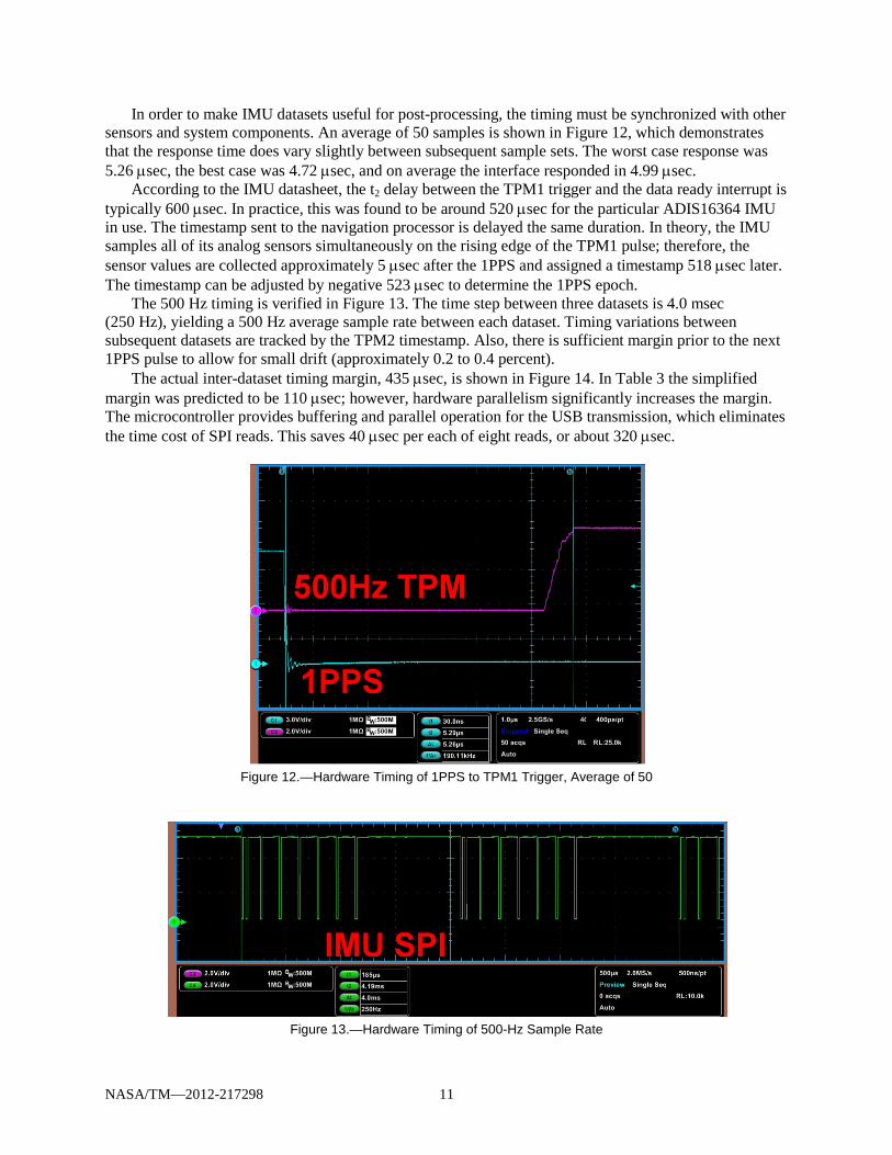
In order to make IMU datasets useful for post-processing, the timing must be synchronized with other sensors and system components. An average of 50 samples is shown in Figure 12, which demonstrates that the response time does vary slightly between subsequent sample sets. The worst case response was 5.26 µsec, the best case was 4.72 µsec, and on average the interface responded in 4.99 µsec.
According to the IMU datasheet, the t2 delay between the TPM1 trigger and the data ready interrupt is typically 600 µsec. In practice, this was found to be around 520 µsec for the particular ADIS16364 IMU in use. The timestamp sent to the navigation processor is delayed the same duration. In theory, the IMU samples all of its analog sensors simultaneously on the rising edge of the TPM1 pulse; therefore, the sensor values are collected approximately 5 µsec after the 1PPS and assigned a timestamp 518 µsec later. The timestamp can be adjusted by negative 523 µsec to determine the 1PPS epoch.
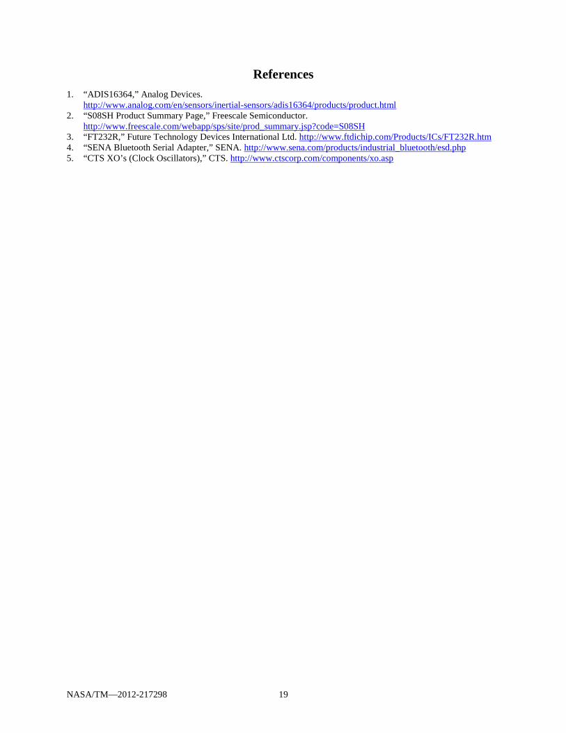
The 500 Hz timing is verified in Figure 13. The time step between three datasets is 4.0 msec (250 Hz), yielding a 500 Hz average sample rate between each dataset. Timing variations between subsequent datasets are tracked by the TPM2 timestamp. Also, there is sufficient margin prior to the next 1PPS pulse to allow for small drift (approximately 0.2 to 0.4 percent).
The actual inter-dataset timing margin, 435 µsec, is shown in Figure 14. In Table 3 the simplified margin was predicted to be 110 µsec; however, hardware parallelism significantly increases the margin. The microcontroller provides buffering and parallel operation for the USB transmission, which eliminates the time cost of SPI reads. This saves 40 µsec per each of eight reads, or about 320 µsec.
Figure 12.—Hardware Timing of 1PPS to TPM1 Trigger, Average of 50
Figure 13.—Hardware Timing of 500-Hz Sample Rate

NASA/TM—2012-217298 12
Figure 14.—Hardware Inter-Dataset Timing Margin
The majority of hardware timing constraints are due to communications delays. There are other
unaccounted factors, such as instruction execution time, which will provide only minimal effect on the dataset timing and are not considered here. The individual dataset timing margin, 435 µsec, would allow transmission of an extra 6 B of data to the navigation processor without significant impact. Or, system sampling could be increased to 638 Hz without reducing the dataset.
Conclusions and Recommendations This paper introduced a microcontroller interface board for an Analog Devices ADIS16364 IMU. The
board supports sampling at 500-Hz with synchronization to a 1PPS pulse with 5 µsec delay on average. The microcontroller firmware is adaptable to similar Analog Devices IMUs and can be modified to accommodate different timing schemes. The circuit provides selectable communication between either the USB or Bluetooth modules at 115200 baud.
The interface board addresses two issues experienced using the previous board: synchronization and data corruption. Synchronization was resolved through the external 1PPS trigger, which allowed all elements of the system to be synchronized to the same pulse. Data corruption primarily was solved through use of an external oscillator that allowed the sampling rate and communications rates to be held relatively constant despite temperature change. These enhancements made it simpler to include the board in an overall navigation system with other sensors.
Two potential design improvements were identified following this revision of the interface board. The Bluetooth module provides a good step toward wireless data transfer, but it does not yet support a 1PPS timing signal. The board would be more useful if 1PPS over-the-air delay could be characterized and implemented. Also, the IMU register reads could be advanced closer to the USB header transmission, which may result in some additional communications time savings. The USB/SCI buffer will likely be empty prior to the initial read of the gyroscope-X register.
Active development of the IMU interface board ended in September 2010.

NASA/TM—2012-217298 13
Appendix A.—Acronyms 1PPS one pulse per second DIP dual in-line package D-RATS Desert Research and Technology Studies GPIO general purpose I/O GPS global positioning system GRC NASA Glenn Research Center I/O input-output IMU inertial measurement unit IRQ interrupt request ISR interrupt service routine LECLDS Lunar Extra-Vehicular Activity Crewmember Location Determination System MEMS microelectromechanical systems MISO master in slave out MOSI master out slave in NASA National Aeronautics and Space Administration PPM parts per million RAM random access memory RTC real time clock SCI serial communications interface SCK serial clock SPI serial peripheral interface SS# inverted logic slave select TPM timer peripheral module TTL transistor-transistor logic UART universal asynchronous receiver-transmitter USB universal serial bus


NASA/TM—2012-217298 15
Appendix B.—Circuit Board Schematic


NASA/TM—2012-217298 17
Appendix C.—Circuit Board Layers (Actual Size)
Bottom Layer, Reversed
Ground Layer
Power Layer

NASA/TM—2012-217298 18
Top Layer
Silkscreen Bottom Layer, Reversed
Silkscreen Top Layer
NASA/TM—2012-217298 19
References
1. “ADIS16364,” Analog Devices. http://www.analog.com/en/sensors/inertial-sensors/adis16364/products/product.html
2. “S08SH Product Summary Page,” Freescale Semiconductor. http://www.freescale.com/webapp/sps/site/prod_summary.jsp?code=S08SH
3. “FT232R,” Future Technology Devices International Ltd. http://www.ftdichip.com/Products/ICs/FT232R.htm 4. “SENA Bluetooth Serial Adapter,” SENA. http://www.sena.com/products/industrial_bluetooth/esd.php 5. “CTS XO’s (Clock Oscillators),” CTS. http://www.ctscorp.com/components/xo.asp

REPORT DOCUMENTATION PAGE Form Approved OMB No. 0704-0188
The public reporting burden for this collection of information is estimated to average 1 hour per response, including the time for reviewing instructions, searching existing data sources, gathering and maintaining the data needed, and completing and reviewing the collection of information. Send comments regarding this burden estimate or any other aspect of this collection of information, including suggestions for reducing this burden, to Department of Defense, Washington Headquarters Services, Directorate for Information Operations and Reports (0704-0188), 1215 Jefferson Davis Highway, Suite 1204, Arlington, VA 22202-4302. Respondents should be aware that notwithstanding any other provision of law, no person shall be subject to any penalty for failing to comply with a collection of information if it does not display a currently valid OMB control number. PLEASE DO NOT RETURN YOUR FORM TO THE ABOVE ADDRESS. 1. REPORT DATE (DD-MM-YYYY) 01-05-2012
2. REPORT TYPE Technical Memorandum
3. DATES COVERED (From - To)
4. TITLE AND SUBTITLE Sampling and Control Circuit Board for an Inertial Measurement Unit
5a. CONTRACT NUMBER
5b. GRANT NUMBER
5c. PROGRAM ELEMENT NUMBER
6. AUTHOR(S) Chelmins, David; Powis, Rick
5d. PROJECT NUMBER
5e. TASK NUMBER
5f. WORK UNIT NUMBER WBS 903184.04.20.03.02.01
7. PERFORMING ORGANIZATION NAME(S) AND ADDRESS(ES) National Aeronautics and Space Administration John H. Glenn Research Center at Lewis Field Cleveland, Ohio 44135-3191
8. PERFORMING ORGANIZATION REPORT NUMBER E-18046
9. SPONSORING/MONITORING AGENCY NAME(S) AND ADDRESS(ES) National Aeronautics and Space Administration Washington, DC 20546-0001
10. SPONSORING/MONITOR'S ACRONYM(S) NASA
11. SPONSORING/MONITORING REPORT NUMBER NASA/TM-2012-217298
12. DISTRIBUTION/AVAILABILITY STATEMENT Unclassified-Unlimited Subject Category: 33 Available electronically at http://www.sti.nasa.gov This publication is available from the NASA Center for AeroSpace Information, 443-757-5802
13. SUPPLEMENTARY NOTES
14. ABSTRACT Spacesuit navigation is one component of NASA’s efforts to return humans to the Moon. Studies performed at the NASA Glenn Research Center (GRC) considered various navigation technologies and filtering approaches to enable navigation on the lunar surface. As part of this effort, microelectromechanical systems (MEMS) inertial measurement units (IMUs) were studied to determine if they could supplement a radiometric infrastructure. MEMS IMUs were included in the Lunar Extra-Vehicular Activity Crewmember Location Determination System (LECLDS) testbed during NASA’s annual Desert Research and Technology Studies (D-RATS) event in 2009 and 2010. The testbed included one IMU in 2009 and three IMUs in 2010, along with a custom circuit board interfacing between the navigation processor and each IMU. The board was revised for the 2010 test, and this paper documents the design details of this latest revision of the interface circuit board and firmware. 15. SUBJECT TERMS Navigation; Circuit boards; Microelectromechanical systems; Firmware; Inertial platforms; Lunar surface
16. SECURITY CLASSIFICATION OF: 17. LIMITATION OF ABSTRACT UU
18. NUMBER OF PAGES
26
19a. NAME OF RESPONSIBLE PERSON STI Help Desk (email:[email protected])
a. REPORT U
b. ABSTRACT U
c. THIS PAGE U
19b. TELEPHONE NUMBER (include area code) 443-757-5802
Standard Form 298 (Rev. 8-98)Prescribed by ANSI Std. Z39-18

