sampled-data modeling and analysis of closed-loop - drum
TRANSCRIPT

ISR develops, applies and teaches advanced methodologies of design and analysis to solve complex, hierarchical,heterogeneous and dynamic problems of engineering technology and systems for industry and government.
ISR is a permanent institute of the University of Maryland, within the Glenn L. Martin Institute of Technol-ogy/A. James Clark School of Engineering. It is a National Science Foundation Engineering Research Center.
Web site http://www.isr.umd.edu
I RINSTITUTE FOR SYSTEMS RESEARCH
TECHNICAL RESEARCH REPORT
Sampled-Data Modeling and Analysis of Closed-Loop PWM DC-DC Converters
by Chung-Chieh Fang, Eyad H. Abed
T.R. 99-24

Sampled-Data Modeling and Analysis
of Closed-Loop PWM DC-DC Converters
Chung-Chieh Fang and Eyad H. AbedDepartment of Electrical Engineering
and the Institute for Systems ResearchUniversity of Maryland
College Park, MD 20742 USA
Manuscript: February 1998; revised in March 1999
Abstract
Sampled-data analysis of converters has been a topic of investigation for the past two decades.However, this powerful tool is not widely used in control loop design or in closed-loop perfor-mance validation. Instead, averaged models are typically used for control loop design, whiledetailed simulations are used for validating closed-loop performance. This paper makes severalcontributions to the sampled-data modeling and analysis of closed-loop PWM DC-DC convert-ers, with the aim of increasing appreciation and use of the method. General models are presentedin a unified and simple manner, while removing simplifying approximations present in previouswork. These models apply both for current mode control and voltage mode control. The gen-eral models are nonlinear. They are used to obtain analytical linearized models, which are inturn employed to obtain local stability results. Detailed examples illustrate the modeling andanalysis in the paper, and point to situations in which the sampled-data approach gives resultssuperior to alternate methods. For instance, it is shown that the sampled-data approach willreliably predict the (local) stability of a converter for which averaging or simulation predictsinstability.
1 Introduction
Sampled-data analysis of converters has been a topic of investigation for the past two decades
[1, 2, 3]. Sampled-data models of converters are accepted to be more accurate than their averaged
counterparts. This can be important especially in studying dynamical behaviors that averaging
is known not to capture well, such as subharmonic instability [4], chaotic phenomena [5, 6, 7, 8],
and steady-state DC offset [9]. However, the powerful sampled-data approach is not widely used
in control loop design or in closed-loop performance validation. Instead, averaged models are
typically used for control loop design, while detailed simulations are used for validating closed-loop
performance. This paper makes several contributions to the sampled-data modeling and analysis
1

of closed-loop PWM DC-DC converters, with the aim of increasing appreciation and use of the
method. General models are presented in a unified and simple manner, while removing simplifying
approximations present in previous work.
Because the dynamical behavior differs for continuous conduction mode (CCM) and discontin-
uous conduction mode (DCM), the general model in CCM differs from that in DCM. However, in
either case the model applies both for current mode control and voltage mode control. Because of
this, the modeling procedure presented here is considered to unify previous disparate contributions
for current mode and voltage mode control.
The general models are nonlinear. They are used to obtain analytical linearized models, which
are in turn employed to obtain local stability results. Detailed examples illustrate the modeling
and analysis in the paper, and point to situations in which the sampled-data approach gives results
superior to alternate methods. For instance, it is shown that the sampled-data approach will reliably
predict the (local) stability of a converter for which averaging or simulation predicts instability.
It is important to clarify at the outset the differences between the contributions to modeling
in this paper in relation to past contributions. In the next paragraph, the relation between the
present work and the original work on sampled-data modeling and analysis of closed-loop PWM
DC-DC converter operation is summarized. This is followed by a summary of the relation between
this work and the literature on sampled-data modeling and analysis of the power stage of a PWM
DC-DC converter.
Lee, Iwens, Yu and Triner [1] and Verghese, Elbuluk and Kassakian [2] are two seminal con-
tributions to sampled-data modeling and analysis of DC-DC converters. These authors developed
general models that apply to closed-loop converter operation. Thus, their results apply also to the
modeling of the power stage of a converter. In relation to these papers, the present contribution
gives more detail, unifies the modeling of current mode control and voltage mode control, and gives
an analytical linearized sampled-data model (not given explicitly in the indicated references). In
addition, the models given here incorporate the exact system trajectory between switching instants.
Tymerski [10, 11] developed general detailed sampled-data models of the power stage of a PWM
2

DC-DC converter. He also obtained an analytical linearized sampled-data model. These papers are
similar to the present work, especially in that they reflect the exact trajectory between switching
instants and include an analytical linearized sampled-data model. The main difference between the
work in [10, 11] and the present paper is that here the closed-loop converter is considered, while in
[10, 11] the power stage is considered.
The paper proceeds as follows. In Section 2, a general block diagram model valid in continuous
conduction mode is given and used to obtain a nonlinear sampled-data model and an associated
linearized model. The linearized model is used to study orbital stability, and to derive the audio-
susceptibility and output impedance. In Section 3, analogous models are given for discontinuous
conduction mode. In Section 4, four examples are given that illustrate application of the models of
the paper to sample converter circuits. In addition, these examples demonstrate advantages of the
sampled-data analysis over averaging and detailed simulation in validating closed-loop performance.
Conclusions are collected in Section 5.
2 Continuous Conduction Mode (CCM)
2.1 Block Diagram Model
In this subsection, a block diagram model for the PWM converter in CCM is proposed. This model
is shown to apply to current mode control and voltage mode control.
Consider, for example, a buck converter under current mode control and voltage mode control,
shown in Fig. 1 and Fig. 2, respectively. They have different control schemes. However, they share
the same characteristics: switching instants are determined by how a ramp signal h(t) intersects
with a feedback signal y(t). This motivates a unified model for both current mode control and
voltage mode control.
The proposed block diagram model for the PWM converter in CCM is shown in Fig. 3. In the
diagram, A1, A2 ∈ RN×N , B1, B2 ∈ RN×2, C,E1, E2 ∈ R1×N , and D ∈ R are constant matrices,
x ∈ RN , y = Cx+Du ∈ R are the state (of power stage and controller) and the feedback signal,
3

+Vs−
+Vo−
L
C R
Error AmplifierVr
Comparator
(Compensating ramp)
Current sensing
+−
y
h(t)+
−
Rs
S R
Q
Clock
Vd−
+
i L
Figure 1: Buck converter under current mode control
+Vs− Vo
+
−
L
C R
Error AmplifierVr
Comparator
Ramp h(t)
y+
−
Vd+
−
i L
Figure 2: Buck converter under voltage mode control
4

respectively. The source voltage is vs; the output voltage is vo. The notation vr denotes the
reference signal, which could be a voltage or current reference. The reference signal vr is allowed
to be time-varying, although it is constant in most applications. The signal h(t) is a T -periodic
ramp with h(0) = Vl and h(T−) = Vh. The clock has the same frequency fs = 1/T as the ramp.
This frequency is called the switching frequency. The two stages in each clock period in CCM are
denoted by S1 and S2. The system is in S1 immediatedly following a clock pulse, and switches to
S2 at instants y(t) = h(t).
S1 :
x = A1x+B1u
vo = E1x
S2 :
x = A2x+B2u
vo = E2x
SwitchingDecision
?
Switch to S1 or S2
- vo
y = Cx+Du
clock
h(t) = Vl + (Vh − Vl)(tT mod 1)
-u = ( )vsvr
Figure 3: A block diagram model for PWM converters in CCM
Assume the switch and the diode in the PWM converter are ideal, so that there is no voltage
drop when they are on. Most PWM converters can be modeled by Fig. 3. The PWM converter
under current mode control fits this model exactly, with h(t) denoting the slope-compensating
ramp. For operation in voltage mode control, the system is switched between stages when the
ramp signal h(t) intersects with the feedback signal y. One of the switchings generally has the
same frequency as the clock. Therefore the model in Fig. 3 is also good for the PWM converter
under voltage mode control. Many other control schemes (e.g., average current mode control) also
fit the model in Fig. 3. Typical waveforms in current and voltage mode control are shown in Fig. 4
and Fig. 5, respectively. Note that in Fig. 4, the ramp has positive slope, instead of negative slope
5
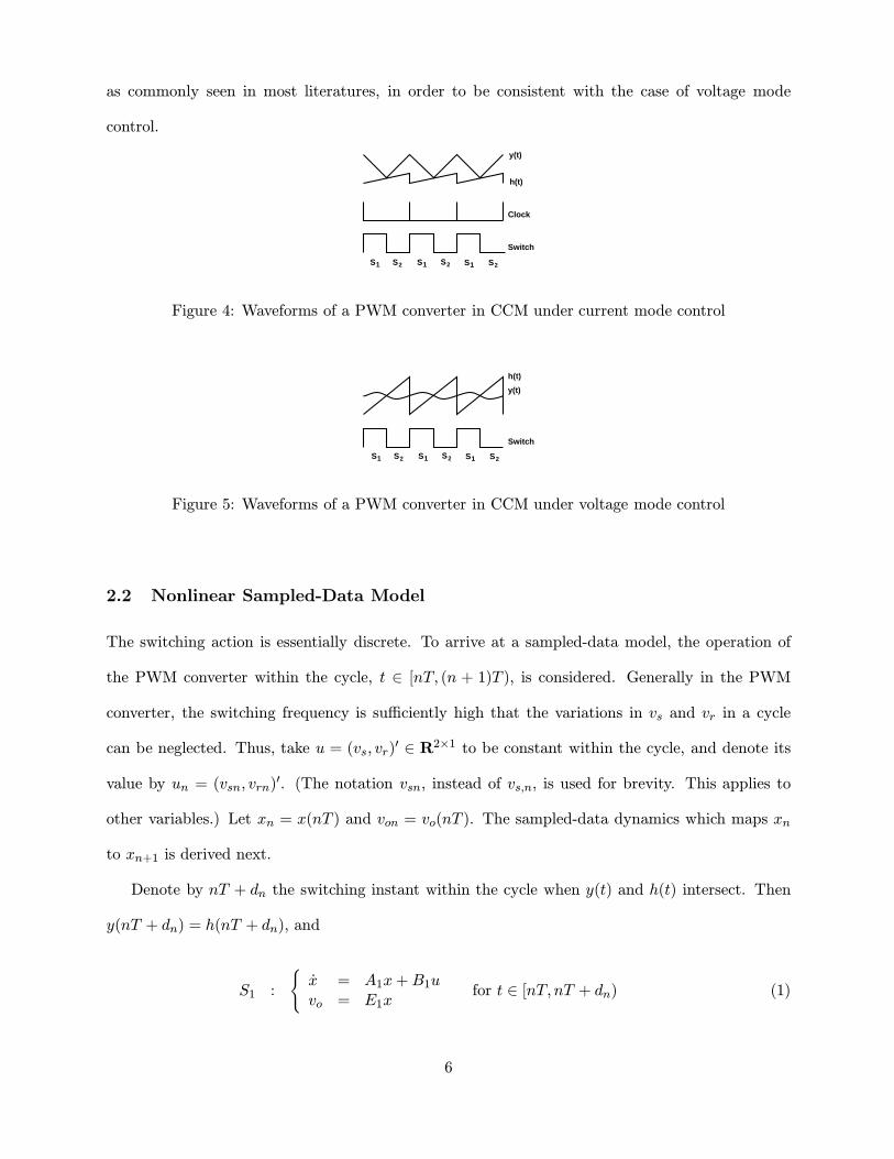
as commonly seen in most literatures, in order to be consistent with the case of voltage mode
control.
h(t)
Clock
Switch
y(t)
S2 S1 S1S1 S2S2
Figure 4: Waveforms of a PWM converter in CCM under current mode control
h(t)
y(t)
Switch
S2 S1 S1S1 S2S2
Figure 5: Waveforms of a PWM converter in CCM under voltage mode control
2.2 Nonlinear Sampled-Data Model
The switching action is essentially discrete. To arrive at a sampled-data model, the operation of
the PWM converter within the cycle, t ∈ [nT, (n + 1)T ), is considered. Generally in the PWM
converter, the switching frequency is sufficiently high that the variations in vs and vr in a cycle
can be neglected. Thus, take u = (vs, vr)′ ∈ R2×1 to be constant within the cycle, and denote its
value by un = (vsn, vrn)′. (The notation vsn, instead of vs,n, is used for brevity. This applies to
other variables.) Let xn = x(nT ) and von = vo(nT ). The sampled-data dynamics which maps xn
to xn+1 is derived next.
Denote by nT + dn the switching instant within the cycle when y(t) and h(t) intersect. Then
y(nT + dn) = h(nT + dn), and
S1 :
x = A1x+B1u
vo = E1xfor t ∈ [nT, nT + dn) (1)
6

S2 :
x = A2x+B2u
vo = E2xfor t ∈ [nT + dn, (n + 1)T ) (2)
The two matrices E1 and E2 need not be the same. For example, they can differ if the equivalent
series resistance (ESR) Rc 6= 0. When they differ, the output voltage is discontinuous. An example
of a discontinuous output voltage waveform is shown in Fig. 6. In most applications, the output
voltage of interest is the maximum, minimum, or average voltage. So in the following, E is used to
denote either E1, E2, or (E1 +E2)/2.
Out
put v
olta
ge
t
E x(nT)1
E x(nT)2
1 2E +E 2
x(nT)
nT (n+1)T
Figure 6: A discontinuous output voltage waveform
Using the dynamics (1) and (2) and the assumption that u = (vs, vr) is constant within the
cycle, one readily obtains the sampled-data dynamics (3)-(5) of the PWM converter in CCM.
The dynamical equation (3) below is augmented with the constraint (4), corresponding to the
intersection condition y(nT + dn) = h(nT + dn) defining dn.
xn+1 = f(xn, un, dn)
= eA2(T−dn)(eA1dnxn +
∫ dn
0eA1(dn−σ)dσB1un) +
∫ T
dn
eA2(T−σ)dσB2un (3)
g(xn, un, dn) = y(nT + dn)− h(nT + dn)
= C(eA1dnxn +
∫ dn
0eA1(dn−σ)dσB1un) +Dun − h(dn)
= 0 (4)
von = Exn (5)
7

2.3 Steady-State Analysis
In the PWM converter, the steady-state operating condition is a periodic solution, not an equi-
librium point as depicted in the averaging method. A T -periodic solution for system in Fig. 3
corresponds to a fixed point for the sampled-data model. A periodic solution x0(t) is sampled as
x0(0). Let the fixed point in the sampled-data dynamics (3)-(5) be (xn, un, dn) = (x0(0), u, d),
where u = (Vs, Vr)′. Then this fixed point satisfies
x0(0) = f(x0(0), u, d) (6)
g(x0(0), u, d) = 0 (7)
where the functions f(·) and g(·) are given in Eqs. (3) and (4). These N + 1 nonlinear equations
(Eqs. (6) and (7)) in N + 1 unknowns (x0(0) and d) can be solved by Newton’s method [1]. After
obtaining x0(0) and d, a periodic solution x0(t) is obtained:
x0(t) =
eA1tx0(0) +
∫ t0 e
A1(t−σ)dσB1u for t ∈ [0, d)
eA2(t−d)x0(d) +∫ td e
A2(t−σ)dσB2u for t ∈ [d, T )x0(t mod T ) for t ≥ T
(8)
A typical periodic solution x0(t) is shown Fig. 7. From Eqs. (1) and (2), x0(d−) = A1x0(d) +B1u
and x0(d+) = A2x0(d) +B2u.
x(d )+0
x(d )-0
0x(d)x(0)0
Figure 7: A typical periodic solution x0(t) of a PWM converter in state space
2.4 Existence of T -Periodic Solutions
Assume all of the eigenvalues of A1 and A2 are in the open left half of the complex plane, then
the matrices I − eA2(T−d)eA1d and I − eA1deA2(T−d) are invertible [12]. From Eq. (6), x0(0) can be
8

expressed as
x0(0) = (I − eA2(T−d)eA1d)−1(eA2(T−d)∫ d
0eA1(d−σ)dσB1u+
∫ T
deA2(T−σ)dσB2u) (9)
Similarly, x0(d) can be expressed as a function of d, denoted as Xs(d):
Xs(d) = (I − eA1deA2(T−d))−1(eA1d∫ T
deA2(T−σ)dσB2u+
∫ d
0eA1(d−σ)dσB1u) (10)
The function Xs(·) has the following property:
Xs(0) = −A−12 B2u (11)
Xs(T ) = −A−11 B1u (12)
So the N + 1 equations, (6) and (7), reduce to one equation in one unknown d:
y(d)− h(d) = CXs(d) +Du− h(d) = 0 (13)
The next result gives a sufficient condition for existence of a fixed point in the sampled-data
dynamics.
Theorem 1 Assume that all of the eigenvalues of A1 and A2 are in the open left half of the complex
plane. If
(CA−12 B2u−Du+ h(0))(CA−1
1 B1u−Du+ h(T−)) ≤ 0 (14)
then there exists a fixed point (xn, un, dn) = (x0(0), u, d) in the sampled-data dynamics (3)-(5).
Proof: From Eq. (13), if
(y(0) − h(0))(y(T−)− h(T−))
= (CXs(0) +Du− h(0))(CXs(T ) +Du− h(T−))
= (CA−12 B2u−Du+ h(0))(CA−1
1 B1u−Du+ h(T−))
≤ 0
9

then by the Intermediate Value Theorem, there exists a solution d ∈ [0, T ) satisfying Eq. (13).
Hence there exists a fixed point (xn, un, dn) = (x0(0), u, d) in the sampled-data dynamics (3)-(5).
2
Note: Whenever there exists a T -periodic solution for the system in Fig. 3, it will be found as
a fixed point in the sampled-data model. However, a fixed point in the sampled-data model may
not correspond to a T -periodic solution in Fig. 3. To explain the last remark, suppose a fixed point
(xn, un, dn) = (x0(0), u, d) is obtained. Then a solution x0(t) can be obtained from Eq. (8). An
example of signals y0(t) := Cx0(t) +Du and h(t) is shown in Fig. 8. The solution y0(t), although
periodic with y0(d) = h(d), cannot be accepted because two switchings occur during t ∈ (0, T ).
d T t
h(t)
y (t)0
Figure 8: Ineligible signals y0(t) and h(t) in voltage mode control
2.5 Linearized Sampled-Data Dynamics
The sampled-data dynamics (3)-(5) is constrained and nonlinear. Assuming that ∂g∂dn
= Cx0(d−)−
h(d) 6= 0, the Implicit Function Theorem allows one to linearize (3)-(5) at the fixed point (xn, un, dn) =
(x0(0), u, d) to obtain an unconstrained linear sampled-data dynamical model. Using a hat ˆ to
denote small perturbations (e.g., xn = xn − x0(0)), it follows that
xn+1 ≈ Φxn + Γunvon = Exn
(15)
where
Φ =∂f
∂xn−
∂f
∂dn(∂g
∂dn)−1 ∂g
∂xn
∣∣∣∣(xn,un,dn)=(x0(0),u,d)
10

= eA2(T−d)(I −((A1 −A2)x0(d) + (B1 −B2)u)C
C(A1x0(d) +B1u)− h(d))eA1d
= eA2(T−d)(I −(x0(d−)− x0(d+))C
Cx0(d−)− h(d))eA1d (16)
Γ =∂f
∂un−
∂f
∂dn(∂g
∂dn)−1 ∂g
∂un
∣∣∣∣(xn,un,dn)=(x0(0),u,d)
= eA2(T−d)(
∫ d
0eA1σdσB1 −
x0(d−)− x0(d+)
Cx0(d−)− h(d)(C
∫ d
0eA1σdσB1 +D)) +
∫ T−d
0eA2σdσB2(17)
Recall that un = (vsn, vrn)′, and denote Γ = [Γ1,Γ2]. Eq. (15) can be rewritten as
xn+1 ≈ Φxn + Γ1vsn + Γ2vrnvon = Exn
(18)
2.6 Stability Analysis
The relevant stability notion is asymptotic orbital stability, not asymptotic stability of an equilib-
rium point as depicted in the averaging method. In the power electronics literature, the PWM
converter is generally said to be either stable or unstable, without mentioning orbital stability per
se. The definition of asymptotic orbital stability is given as follows.
Definition 1 (see, e.g., [13]) Denote by γ the closed orbit generated by the periodic solution x0(t).
Then x0(t) is asymptotically orbitally stable if there is a δ such that
dist[x(0), γ] < δ ⇒ limt→∞
dist[x(t), γ] = 0
where dist[z, γ] is defined as the smallest distance between the point z and any point on γ.
The orbital stability is related to the the set of eigenvalues of Φ, denoted by σ[Φ]. Recall the
following basic results on asymptotic orbital stability of the periodic solution x0(t).
Theorem 2 [13] The fixed point x0(0) of the system (3)-(5) is asymptotically stable, or equivalently
the periodic solution x0(t) in the original continuous-time system of Fig. 3 is asymptotically orbitally
11

stable if all of the eigenvalues of Φ are inside the unit circle of the complex plane. Moreover, if
x0(t) is asymptotically orbitally stable, then no eigenvalues of Φ lies outside the unit circle.
The following well known fact from linear algebra [14, p. 667] will be used in the proofs below.
Lemma 1 If A and B are conformable rectangular matrices, then
det[I +AB] = det[I +BA]
The preceding theorem and lemma will be used to show the following.
Theorem 3 If the periodic solution x0(t) is asymptotically orbitally stable, then the following in-
equality holds: ∣∣∣∣∣Cx0(d+)− h(d)
Cx0(d−)− h(d)
∣∣∣∣∣ ≤ etr[A2−A1]d−tr[A2]T (19)
Equivalently, if (19) does not hold, then the periodic solution x0(t) is not asymptotically orbitally
stable.
Proof: Suppose the periodic solution x0(t) is asymptotically orbitally stable. Then all the eigenval-
ues of Φ have magnitude less than or equal than 1. Since det[Φ] is the product of the eigenvalues
of Φ, it follows that
|det[Φ]| =
∣∣∣∣∣det[eA1deA2(T−d)] det[I −(x0(d−)− x0(d+))C
Cx0(d−)− h(d)]
∣∣∣∣∣=
∣∣∣∣∣det[eA1deA2(T−d)] det[1−C(x0(d−)− x0(d+))
Cx0(d−)− h(d)]
∣∣∣∣∣= e−tr[A2−A1]d+tr[A2]T
∣∣∣∣∣Cx0(d+)− h(d)
Cx0(d−)− h(d)
∣∣∣∣∣≤ 1
where the second line of the calculation follows from Lemma 1. 2
12

Remark: Inequality (19) is a necessary (but not sufficient) condition for stability. Generally the
switching period is so small that the right side of (19) can be approximated as 1, resulting in a
condition that resembles a well-known stability criterion in current mode control [15, for example]:
∣∣∣∣m2 −mc
m1 −mc
∣∣∣∣ < 1 (20)
where m1 is the (positive) slope of the inductor current trajectory during the on stage and m2 is
the (negative) slope during the off stage using a linear approximation [16]; and mc is the (negative)
slope of the compensating ramp. (Note that here m1 > 0, m2 < 0 and mc ≤ 0, which differs from
most literatures’ notations: m1 > 0, m2 > 0 and mc ≥ 0.) Theorem 3 differs from (20) in its use
of instantaneous, rather than approximate, slope. Also, Cx0(t) in Theorem 3 is composed of more
state signals (up to N) than just inductor current.
The next result asserts that a closed-loop pole is zero if the ramp has slope Cx0(d+) =
C(A2x0(d) +B2u).
Theorem 4 If the ramp slope h(d) = Cx0(d+), then the matrix Φ has a zero eigenvalue.
Proof: From the proof in Theorem 3, it can be seen that if h(d) = Cx0(d+), then det[Φ] = 0 and
hence the matrix Φ has a zero eigenvalue. 2
Remark: Generally, a ramp with slope Cx0(d+) is considered to produce deadbeat behavior
(finite settling time) [15, p. 418]. This requires all of the N closed-loop poles to be at 0. Theorem
4 predicts that if the ramp has slope Cx0(d+), then one eigenvalue is 0. Indeed, examples can be
constructed showing that not necessarily all the eigenvalues vanish. Deadbeat behavior is therefore
not guaranteed.
Theorem 5 and Corollary 2 below address the case in which the switching frequency goes to
infinity. The following corollary of Lemma 1 is used in the proof of Theorem 5.
Corollary 1 Let a and b be column vectors of the dimension N . Then one eigenvalue of the square
matrix ab′ is b′a, and the remaining N − 1 eigenvalues are zero.
13

Proof:
det[λI − ab′] = λN det[I −ab′
λ] (21)
= λN det[1−b′a
λ] (22)
= λN (1−b′a
λ) (23)
= λN−1(λ− b′a), (24)
where the second line follows from Lemma 1. 2
Theorem 5 As the switching frequency fs goes to infinity, an eigenvalue of Φ asymptotically ap-
proaches Cx0(d+)−h(d)
Cx0(d−)−h(d)and the remaining (N − 1) eigenvalues approach 1.
Proof: As the switching frequency fs goes to infinity, both eA2(T−d) and eA1d approach identity
matrices. Eq. (16) now implies that Φ approaches (I − (x0(d−)−x0(d+))C
Cx0(d−)−h(d)). Note that the matrix
(x0(d−)− x0(d+))C is the product of a column vector and a row vector, so that Corollary 1 applies.
Thus this matrix has an eigenvalue at C(x0(d−)−x0(d+)) and (N−1) eigenvalues at 0. This in turn
implies that the matrix I− (x0(d−)−x0(d+))C
Cx0(d−)−h(d)has an eigenvalue at 1− C(x0(d−)−x0(d+))
Cx0(d−)−h(d)= Cx0(d+)−h(d)
Cx0(d−)−h(d)
and (N − 1) eigenvalues at 1. 2
Remark: Generally the averaged model is reliable for sufficiently high switching frequency [9].
This theorem implies that the stability criterion in (20) does indeed provide a necessary condition
for stability when the switching frequency is sufficiently high.
Corollary 2 Assume the switching frequency goes to infinity and Cx0(d−) < h(d) (which is gen-
erally true). If (i) Cx0(d+) < Cx0(d−) or (ii) h(d) < C(x0(d+)+x0(d−))2 , then the system is not
asymptotically stable.
Proof: Under the stated assumptions, it can be proved that the eigenvalue Cx0(d+)−h(d)
Cx0(d−)−h(d)is greater
than 1 under condition (i), or less than -1 under condition (ii). Thus, the system is not asymptot-
14

ically stable. 2
Remark: The corollary asserts that if the switching frequency is high and if the slopes of the
output variable y = Cx are not properly set in the design (condition (i)) or if the ramp slope is
not large enough (condition (ii)), the system will be unstable.
2.7 Comparison with Stability Analysis Using State-Space Averaging
The duty cycle changes from cycle to cycle. This variable determines when the switch is on or
off, and it is crucial in the system dynamics. So this variable needs to be modeled properly. The
averaging method, however, treats the duty cycle as a continuous-time variable.
Next, stability analysis using the averaging method is briefly summarized. For details, the
reader is referred to [15]. Let the duty cycle in the averaging method be dc, with nominal value
Dc. Also let
Aave := AONDc +AOFF(1−Dc) (25)
Bave := BONDc +BOFF(1−Dc) (26)
Eave = EONDc +EOFF(1−Dc) (27)
Xave = −A−1aveBaveVs (28)
The nominal solution by the averaging method is Xave, a constant instead of a periodic solution
x0(t). Linearized around the nominal operating point (x, u, dc) = (Xave, (Vs, Vr)′,Dc), the system
in Fig. 3 has the following linearized continuous-time dynamics
˙x ≈ Aavex+Baveu+ ((AON −AOFF)Xave + (BON −BOFF)u)dc (29)
y = Cx+Du (30)
vo = Eavex+ (EON −EOFF)dc (31)
with
dc =
y
Vh−Vl= y
h(d)T(for trailing-edge modulation, because dc = y−Vl
Vh−Vl)
−yVh−Vl
= −yh(d)T
(for leading-edge modulation, because dc = Vh−yVh−Vl
)(32)
15

In either trailing-edge modulation (S1: switch on, S2: off) or leading-edge modulation (S1: off,
S2: on), Substituting Eqs. (29) and (32) into Eq. (29) gives
˙x ≈ Ax+ Bu (33)
where (stage S1 or S2 can be either on or off stage)
A = Aave + ((A1 −A2)Xave + (B1 −B2)u)C
h(d)T(34)
B = Bave + ((A1 −A2)Xave + (B1 −B2)u)D
h(d)T(35)
The system is asymptotically stable if all of the eigenvalues of A are in the open left half of the
complex plane, which is equivalent to all of the eigenvalues of exp(AT ) being inside the unit circle.
From Eq. (34), exp(AT ) can be written as (for either trailing-edge or leading-edge modulation)
exp(AT ) = eA2(T−d)+A1d+
((A1−A2)Xave+(B1−B2)u)C
h(d) (36)
which is similar in form to Φ in Eq. (16).
Comparing Eqs. (36) and (16), it is seen that the averaging method agrees with the sampled-
data method under the following conditions:
1. x0(d) is approximated by Xave (true if the periodic solution x0(t) is approximated by the
equilibrium Xave).
2. Cx0(d−) is much smaller than h(d).
3. T is very small, so that e(x0(d−)−x0(d+))CT ≈ I + (x0(d−)− x0(d+))CT .
4. The matrices A1, A2 and (x0(d−)− x0(d+))C commute.
Note that condition 4 is unlikely to hold, and condition 2 generally does not hold for current mode
control.
2.8 Closed-Loop Audio-Susceptibility and Output Impedance
Audio-Susceptibility and output impedance are expressed in terms of transfer functions (frequency
responses). They give information on the effect of (source or load) disturbances at various frequen-
16

cies on the output voltage.
The audio-susceptibility is derived directly from the linearized sampled-data model, Eq. (18).
It is
Tos(z) =vo(z)
vs(z)= E(zI − Φ)−1Γ1 (37)
To calculate the output impedance, add a fictitious current source io (as perturbation) in parallel
with the load. Then the state equations in Eqs. (1) and (2) are replaced by
S1 : x = A1x+B11vs +B12vr +B13io (38)
S2 : x = A2x+B21vs +B22vr +B23io (39)
where B13, B23 ∈ RN×1.
Since io is used as perturbation, the nominal value of io is 0. Similar to the derivation in
Section 2.2, the new linearized sampled-data dynamics is
xn+1 ≈ Φxn + Γ1vsn + Γ2vrn + Γ3ionvon = Exn
(40)
where
Γ3 =∂f
∂ion−
∂f
∂dn(∂g
∂dn)−1 ∂g
∂ion
∣∣∣∣(xn,u,dn,ion)=(x0(0),u,d,0)
= eA2(T−d)(
∫ d
0eA1σdσB13 −
x0(d−)− x0(d+)
Cx0(d−)− h(d)C
∫ d
0eA1σdσB13)
∫ T−d
0eA2σdσB23 (41)
and ion is the sampled perturbed output current. So the output impedance is
Too(z) =vo(z)
io(z)= E(zI − Φ)−1Γ3 (42)
Given a transfer function in z domain, say T (z), its effective frequency response [17, p. 93] is
T (ejωT ), which is valid in the frequency range |ω| < πT .
17

3 Discontinuous Conduction Mode (DCM)
3.1 Block Diagram Model
There are three stages in DCM in a cycle. The first two stages and their operation are the same
as in CCM. The system is switched to the third stage when the inductor current iL reaches zero.
Within the third stage, iL = 0. A block diagram model for the PWM converter in DCM is shown
in Fig. 9. The matrix F ∈ R1×N is chosen such that Fx = iL. The remaining notation is the same
as in Fig. 3.
S1 :
x = A1x+B1u
vo = E1x
S2 :
x = A2x+B2u
vo = E2x
S3 :
x = A3x+B3u
vo = E3x
SwitchingDecision
?
Switch to S1, S1, or S3
- vo
iL = Fx
y = Cx+Du
clock
h(t) = Vl + (Vh − Vl)(tT mod 1)
-u = ( )vsvr
Figure 9: A block diagram model for PWM converters in DCM
3.2 Nonlinear Sampled-Data Model
Consider the operation of the PWM converter within the cycle, t ∈ [nT, (n + 1)T ). As in CCM,
take u = (vs, vr)′ to be constant within the cycle and denote its value by un = (vsn, vrn)′.
Denote by nT + d1n the switching instant when y(t) and h(t) intersect within the cycle. (The
notation d1n, instead of d1,n, is used for brevity.) Denote by nT + d2n the switching instant when
18

the inductor current reaches zero. The three stages S1, S2, S3 within the cycle are thus
S1 :
x = A1x+B1u
vo = E1xfor t ∈ [nT, nT + d1n) (43)
S2 :
x = A2x+B2u
vo = E2xfor t ∈ [nT + d1n, nT + d2n) (44)
S3 :
x = A3x+B3u
vo = E3xfor t ∈ [nT + d2n, (n + 1)T ) (45)
The two switching conditions (at t = nT + d1n and nT + d2n) are
y(nT + d1n) = Cx(nT + d1n) +Dun = h(nT + d1n) (46)
iL(nT + d2n) = Fx(nT + d2n) = 0 (47)
As in CCM, the output voltage in DCM can be discontinuous at the clock time. Again, E is
used to denote E1, E3, or (E1 +E3)/2 depending on which value of output voltage is of interest.
From Eqs. (43)-(47), the PWM converter in DCM has the following sampled-data dynamics:
xn+1 = f(xn, un, dn)
= eA3(T−d2n)(eA2(d2n−d1n)(eA1d1nxn +
∫ d1n
0eA1(d1n−σ)dσB1un)
+
∫ d2n
d1n
eA2(d2n−σ)dσB2un) +
∫ T
d2n
eA3(T−σ)dσB3un (48)
von = Exn (49)
g(xn, un, dn) =
[Cx(nT + d1n) +Dun − h(nT + d1n)
Fx(nT + d2n)
]
=
[C(eA1d1nxn +
∫ d1n0 eA1σdσB1un) +Dun − h(d1n)
F (eA2(d2n−d1n)(eA1d1nxn +∫ d1n0 eA1σdσB1un) +
∫ d2n−d1n0 eA2σdσB2un)
]
= 0 (50)
where dn = (d1n, d2n)′. Since the inductor current always starts from 0 at the beginning of a cycle,
another explicit constraint is Fxn = iLn = 0, for any n. So the dynamics is (N -1)-dimensional
19

instead of N -dimensional.
3.3 Linearized Sampled-Data Dynamics
Linearizing Eqs. (48)-(50) and using the notation to denote evaluation at the fixed point (xn, un, dn) =
(x0(0), u, (d1, d2)′), one has
xn+1 ≈ Φxn + Γunvon = Exn
(51)
where
Φ =∂f
∂xn−
∂f
∂dn(∂g
∂dn)−1 ∂g
∂xn
∣∣∣∣
(52)
Γ =∂f
∂un−
∂f
∂dn(∂g
∂dn)−1 ∂g
∂un
∣∣∣∣
(53)
∂f
∂xn
∣∣∣∣
= eA3(T−d2)eA2(d2−d1)eA1d1 (54)
∂f
∂dn
∣∣∣∣
= eA3(T−d2)[eA2(d2−d1)(x0(d−1 )− x0(d+
1 )) x0(d−2 )− x0(d+2 )
](55)
∂g
∂dn
∣∣∣∣
=
[Cx0(d−1 )− h(d1) 0
FeA2(d2−d1)(x0(d−1 )− x0(d+1 )) Fx0(d−2 )
](56)
∂g
∂xn
∣∣∣∣
=
[C
FeA2(d2−d1)
]eA1d1 (57)
∂f
∂un
∣∣∣∣
= eA3(T−d2)(eA2(d2−d1)∫ d1
0eA1σdσB1 +
∫ d2−d1
0eA2σdσB2) +
∫ T−d2
0eA3σdσB3 (58)
∂g
∂un
∣∣∣∣
=
[C∫ d10 eA1σdσB1 +D
F (eA2(d2−d1)∫ d10 eA1σdσB1 +
∫ d2−d10 eA2σdσB2)
](59)
Since the inductor current iL starts at 0 and ends at 0 in any cycle, it is not a dynamic variable.
Thus, the dimension of the dynamics can be reduced by one. Note that this also implies that Φ
possesses a zero eigenvalue, i.e. that det[Φ] = 0. This is shown in detail as follows:
det[Φ] = det[eA3(T−d2)eA2(d2−d1)(I −[x0(d−1 )− x0(d+
1 ) e−A2(d2−d1)(x0(d−2 )− x0(d+2 ))
]·
20

(∂g
∂dn)−1
∣∣∣∣
[C
FeA2(d2−d1)
])eA1d1 ]
= det[eA1d1eA3(T−d2)eA2(d2−d1)] det[I −
[C
FeA2(d2−d1)
]·
[x0(d−1 )− x0(d+
1 ) e−A2(d2−d1)(x0(d−2 )− x0(d+2 ))
](∂g
∂dn)−1
∣∣∣∣]
= det[eA1d1eA3(T−d2)eA2(d2−d1)] ·
det[I −
[C(x0(d−1 )− x0(d+
1 )) Ce−A2(d2−d1)(x0(d−2 )− x0(d+2 ))
FeA2(d2−d1)(x0(d−1 )− x0(d+1 )) Fx0(d−2 )
]·
[Fx0(d−2 ) 0
−FeA2(d2−d1)(x0(d−1 )− x0(d+1 )) Cx0(d−1 )− h(d1)
](Cx0(d−1 )− h(d1))Fx0(d−2 )
]
= det[eA1d1eA3(T−d2)eA2(d2−d1)] det[I −
[∗ ∗0 1
]]
= 0
here ∗ signifies an irrelevant term.
The stability, audio-susceptibility and output impedance analysis are similar to the case in CCM
and are omitted.
4 Illustrative Examples
Example 1 (Local vs. global orbital stability, [9, p. 90]) Consider the boost converter shown in
Fig. 10, where T = 2µs, Vs = 4V , L = 5.24µH, C = 0.2µF , R = 16Ω, k1 = −0.1, k2 = 0.01,
Vr = 0.48V , and h(t) = (( tT ) mod 1).
Although the control scheme is neither voltage nor current mode control, the circuit can still
be expressed in terms of the block diagram model in Fig. 3, with state x = (iL, vC)′:
A1 =
[0 00 −1
RC
]A2 =
[0 −1
L1C
−1RC
]B1 = B2 =
[1L
0
]C =
[−k1 −k2
]D =
[0 1
]E1 = E2 =
[0 1
]21

The periodic solution calculated using Eq. (8) is shown in Fig. 11. The closed-loop poles
calculated from Eq. (16) are σ(Φ) = 0.8 ± 0.45i, which are inside the unit circle. So the periodic
solution is locally orbitally stable. The magnitude of the eigenvalues is 0.9225, indicating that the
settling time to the steady state may be long. For example, let the initial state be (iL, vC)′ =
(0.9, 8)′. The simulated output voltage is shown in Fig. 12. After the transient, the state trajectory
goes to the periodic solution.
The averaging method also predicts local stability (but not local orbital stability). From Sec-
tion 2.7, the closed-loop poles predicted by the averaging method are
σ(A) = (−0.2759 ± 2.9276i) × 105 (60)
and eσ(A)T = 0.7887 ± 0.5230i, close to the eigenvalues found above using by the sampled-data
method.
However, the circuit is not globally stable and is described in [9] as being unstable based on
simulation. Since the averaging method is for local (small-signal) analysis, it is not surprising that
it cannot predict lack of global stability.
Comparator
−
y+
+Vs−
+Vo−
L
C R
i L
Vc
+
−
Vr
−−
+
h(t)
1k 2k
Figure 10: System diagram for Example 1
Example 2 (Buck converter under voltage mode phase-lead control, [15, p. 346]) The system
diagram is shown in Fig. 13. The system parameters are as follows: T = 10µs, Vs = 28V , R = 3Ω,
22

0.5 1 1.5 27
7.5
8
8.5
9
9.5
10
10.5
11
11.5
12
Inductor Current (A)
Cap
acito
r V
olta
ge (
V)
Figure 11: Periodic solution in Example 1
0 0.2 0.4 0.6 0.8 1 1.2
x 10−4
0
2
4
6
8
10
12
14
16
18
20
t (Sec)
Vo
(Vol
t)
Figure 12: Output voltage trajectory in Example 1 for initial condition (iL, vC)′ = (0.9, 8)′
23

L = 50µH, C = 500µF , Vr = 5V , Gc0 = 3.7, ωz = 10681 rad/sec, ωp = 91106 rad/sec, and
h(t) = 4( tT mod 1). The voltage divider gain gvd is chosen to be 0.29465 (instead of 1/3 in [15]) to
result in an output voltage at 15V .
+Vs−
+Vo−
L
C R
Vr
Comparator
h(t)
y
g vd
+
-
s1 +z
1 + sp
Gc0ω
ω( )
+
-
+Vc-
i L
Figure 13: System diagram for Example 2
Let the state x = (iL, vC , xc)′, where xc is the state of the error amplifier. In terms of the
representation in Fig. 3, one has
A1 = A2 =
0 −1L 0
1C
−1RC 0
0 gvd(ωp − ωz) −ωp
B1 =
1L 00 00 ωz − ωp
B2 =
0 00 00 ωz − ωp
C =
Gc0ωpωz
[0 −gvd 1
]D =
[0
Gc0ωpωz
]E1 = E2 =
[0 1 0
]
Solving Eqs. (9) and (13) by Newton’s method results in x0(0) = (4.3, 15,−0.512)′ and d =
5.36 × 10⁻⁶. The eigenvalues of the closed-loop system can be obtained from σ[Φ] and they are
0.8096 ± 0.1154 and 0.5973. All of them are inside the unit circle, so the periodic solution x0(t) is
asymptotically orbitally stable.
Example 3 (Boost converter under current mode control with voltage loop closed, [18]) The
system diagram is shown in Fig. 14, where fs = 25kHz, Vs = 28V , R = 11.2Ω, L = 195µH,
24

C = 2mF , R1 = 47.5kΩ, R2 = 2.5kΩ, Rs = 0.8125Ω, Rf = 72.2kΩ, and Cf = 0.23µF . The
reference voltage Vr and thus the duty cycle are varied. The system is analyzed for two situations:
without slope compensation (h(t) = 0), and with slope compensation (h(t) = (RsVsT5L )[ tT mod 1]).
Let the state x = (iL, vC , vcf )′. The system matrices in Fig. 3.1 are
A1 =
0 0 00 −1
RC 00 −1
CfR10
A2 =
0 −1L 0
1C
−1RC 0
0 −1CfR1
0
B1 = B2 =
1L 00 00 1
CfR1+ 1
CfR2
C =
[−Rs
−RfR1
1]
D =[
0 1 +RfR1
+RfR2
]E1 = E2 =
[0 1 0
]
First, consider the system without slope compensation. The duty cycle is varied (for different
Vr) from 0.4 to 0.6 and σ[Φ] is plotted and shown in Fig. 15. One eigenvalue trajectory crosses the
unit circle at Dc = 0.498. The other two remain very close to 1. For Dc > 0.498, the system is
unstable.
Next, consider the system with slope compensation. The duty cycle is varied from 0.4 to 0.7
and σ[Φ] is calculated. One eigenvalue trajectory crosses the unit circle at Dc = 0.5845. For
Dc > 0.5845, the system is unstable.
In [18], the system is reported to be unstable for Dc > 0.454 without slope compensation and
for Dc > 0.61 with slope compensation.
Example 4 (Boost converter under current mode control, [19]) Consider the same boost con-
verter as in Example 3, with the following differences: here fs = 100kHz, Vr = 1.8V , h(t) = 0
and parasitic resistances in the switch, diode, inductor, and capacitor are modeled and are given
by RQ = 0.055Ω, RD = 0.011Ω, RI = 0.03Ω, Rc = 0.012Ω, respectively. With these choices, the
system is studied in [19] and shown to be stable. However, both state-space average model and an
improved model [20] predict the system to be unstable.
Let the state x = (iL, vC , vcf )′. As in [19], let α = R/(R + Rc) and β = αRc. The system
25

R1
R2
Vr
Comparator+
−y
h(t)+
−
Rs
S R
Q −
+
Cf Rf
+Vs−
+Vo−
L
C R
i L
Vc
+
−
Clock
+ Vcf −
Figure 14: System diagram for Example 3
−1.5 −1 −0.5 0 0.5 1
−1
−0.8
−0.6
−0.4
−0.2
0
0.2
0.4
0.6
0.8
1
Dc=0.4D
c=0.6
Figure 15: σ(Φ) as Dc varies from 0.4 to 0.6
26

matrices in Fig. 3.1 are
A1 =
−(RI+RQ+Rs)
L 0 00 −1
(R+Rc)C0
0 −αCfR1
0
A2 =
−(RI+RD+β)
L−αL 0
αC
−1(R+Rc)C
0−βCfR1
−αCfR1
0
B1 = B2 =
1L 00 00 1
CfR1+ 1
CfR2
C =
[−Rs
−RfαR1
1]
D =[
0 1 +RfR1
+RfR2
]E1 =
[0 α 0
]E2 =
[β α 0
]
The closed-loop poles (σ[Φ]) are calculated as -0.3383, 0.9928 and 0.9994. Thus, the sampled-
data approach gives a better indication of stability than the averaged model.
5 Concluding Remarks
General sampled-data modeling and analysis were performed for closed-loop PWM DC-DC convert-
ers. The models unify past work, while removing simplifying approximations. They apply both for
current mode control and voltage mode control. Linearized models were derived analytically, and
used to perform associated calculations, among which are general results on stability. Examples
were used to show that the sampled-data approach will reliably predict the (local) stability of a
converter for which averaging or simulation predicts instability. Thus, sampled data models should
be viewed as an important tool for closed-loop performance validation. It is hoped that this work
will help to facilitate further applications of the sampled-data approach in power electronics.
Acknowledgments
This research has been supported in part by the the Office of Naval Research under Multidisci-plinary University Research Initiative (MURI) Grant N00014-96-1-1123, the U.S. Air Force Officeof Scientific Research under Grant F49620-96-1-0161, and by a Senior Fulbright Scholar Award.
References
[1] F.C.Y. Lee, R.P. Iwens, Yuan Yu, and J.E. Triner, “Generalized computer-aided discretetime-domain modeling and analysis of DC-DC converters,” IEEE Transactions on IndustrialElectronics and Control Instrumentation, vol. IECI-26, no. 2, pp. 58–69, 1979.
27

[2] G.C. Verghese, M. Elbuluk, and J.G. Kassakian, “A general approach to sample-data modelingfor power electronic circuits,” IEEE Transactions on Power Electronics, vol. 1, no. 2, pp. 76–89, 1986.
[3] R. Lutz and M. Grotzbach, “Straightforward discrete modelling for power converter systems,”in IEEE Power Electronics Specialists Conference Record, 1986, pp. 761–770.
[4] A.R. Brown and R.D. Middlebrook, “Sampled-data modelling of switching regulators,” inIEEE Power Electronics Specialists Conference Record, 1981, pp. 349–369.
[5] J.H.B. Deane and D.C. Hamill, “Instability, subharmonics, and chaos in power electronicscircuits,” IEEE Transactions on Power Electronics, vol. 5, no. 3, pp. 260–268, 1990.
[6] D.C. Hamill, J.H.B. Deane, and J. Jefferies, “Modeling of chaotic DC-DC converters byiterated nonlinear mappings,” IEEE Transactions on Power Electronics, vol. 7, no. 1, pp.25–36, 1992.
[7] J.H.B. Deane, “Chaos in a current-mode controlled boost DC-DC converter,” IEEE Trans-actions on Circuits and Systems-I: Fundamental Theory and Applications, vol. 39, no. 8, pp.680–683, 1992.
[8] C.K. Tse, “Flip bifurcation and chaos in three-state boost switching regulators,” IEEETransactions on Circuits and Systems-I: Fundamental Theory and Applications, vol. 41, no. 1,pp. 16–23, 1994.
[9] B. Lehman and R.M. Bass, “Switching frequency dependent averaged models for PWM DC-DC converters,” IEEE Transactions on Power Electronics, vol. 11, no. 1, pp. 89–98, 1996.
[10] R. Tymerski, “Frequency analysis of time-interval-modulated switched networks,” IEEETransactions on Power Electronics, vol. 6, no. 2, pp. 287–295, 1991.
[11] R. Tymerski, “Application of the time-varying transfer function for exact small-signal analy-sis,” IEEE Transactions on Power Electronics, vol. 9, no. 2, pp. 196–205, 1994.
[12] C.-C. Fang, Sampled-Data Analysis and Control of DC-DC Switching Convert-ers, Ph.D. thesis, University of Maryland, College Park, 1997, available athttp://www.isr.umd.edu/TechReports/ISR/1997/.
[13] H.K. Khalil, Nonlinear Systems, Macmillan, New York, 1992.
[14] K. Ogata, Discrete-Time Control Systems, Prentice Hall, Englewood Cliffs, NJ, Second edition,1995.
[15] R.W. Erickson, Fundamentals of Power Electronics, Chapman and Hall, New York, 1997.
[16] R.D. Middlebrook and S. Cuk, “A general unified approach to modelling switching-converterpower stages,” in IEEE Power Electronics Specialists Conference Record, 1976, pp. 18–34.
[17] A.V. Oppenheim and R.W. Schafer, Discrete-Time Signal Processing, Prentice-Hall, Engle-wood Cliffs, NJ, 1989.
[18] I. Zafrany and S. Ben-Yaakov, “A chaos model of subharmonic oscillations in current modePWM boost converters,” in IEEE Power Electronics Specialists Conference Record, 1995, pp.1111–1117.
28

[19] R.M. Bass, B.S. Heck, and R.A. Khan, “Average modelling of current-mode controlled convert-ers: instability predictions,” International Journal of Electronics, vol. 77, no. 5, pp. 613–628,1994.
[20] F.D. Tan and R.D. Middlebrook, “A unified model for current-programmed converters,” IEEETransactions on Power Electronics, vol. 10, no. 4, pp. 397–408, 1995.
29