sa56004x smbus-compatible, 8-pin, remote/local digital ... · temperature sensor with...
TRANSCRIPT
1. General description
The NXP Semiconductors SA56004X is an SMBus compatible, 11-bit remote/local digital temperature sensor with overtemperature alarms. The remote channel of the SA56004X monitors a diode junction, such as a substrate PNP of a microprocessor or a diode connected transistor such as the 2N3904 (NPN) or 2N3906 (PNP). With factory trimming, remote sensor accuracy of 1 C is achieved.
Undertemperature and overtemperature alert thresholds can be programmed to cause the ALERT output to indicate when the on-chip or remote temperature is out of range. This output may be used as a system interrupt or SMBus alert. The T_CRIT output is activated when the on-chip or remote temperature measurement rises above the programmed T_CRIT threshold register value. This output may be used to activate a cooling fan, send a warning or trigger a system shutdown. To enhance system reliability further, the SA56004X employs an SMBus time-out protocol. The SA56004X has a unique device architecture.
The SA56004X is available in the SO8, TSSOP8 and HVSON8 packages. SA56004X has 8 factory-programmed device address options. The SA56004X is pin-compatible with the LM86, MAX6657/8, and ADM1032.
2. Features and benefits
Accurately senses temperature of remote microprocessor thermal diodes or diode connected transistors within 1 C
On-chip local temperature sensing within 2 C Temperature range of 40 C to +125 C 11-bit, 0.125 C resolution
8 different device addresses are available for server applications. The SA56004ED with marking code 56004E, and SA56004EDP with marking code 6004E are address compatible with the National LM86, the MAX6657/8 and the ADM1032.
Offset registers available for adjusting the remote temperature accuracy
Programmable under/overtemperature alarms: ALERT and T_CRIT
SMBus 2.0 compatible interface, supports TIMEOUT
Operating voltage range: 3.0 V to 3.6 V
I2C-bus Standard-mode and Fast-mode compatible
SO8, TSSOP8 and HVSON8 packages
Programmable conversion rate (0.0625 Hz to 26 Hz)
Undervoltage lockout prevents erroneous temperature readings
Latch-up testing is done to JEDEC Standard JESD78 which exceeds 100 mA
SA56004XSMBus-compatible, 8-pin, remote/local digital temperature sensor with overtemperature alarmsRev. 7 — 25 February 2013 Product data sheet

NXP Semiconductors SA56004XDigital temperature sensor with overtemperature alarms
3. Applications
System thermal management in laptops, desktops, servers and workstations
Computers and office electronic equipment
Electronic test equipment and instrumentation
HVAC
Industrial controllers and embedded systems
4. Ordering information
[1] There are 8 device slave address options, as described in Table 4.
Table 1. Ordering information
Type number[1] Topside marking
Package
Name Description Version
SA56004AD 56004AD SO8 plastic small outline package; 8 leads; body width 3.9 mm SOT96-1
SA56004BD 56004BD
SA56004CD 56004CD
SA56004DD 56004DD
SA56004ED 56004ED
SA56004FD 56004FD
SA56004GD 56004GD
SA56004HD 56004HD
SA56004ADP 6004A TSSOP8 plastic thin shrink small outline package; 8 leads; body width 3 mm SOT505-1
SA56004BDP 6004B
SA56004CDP 6004C
SA56004DDP 6004D
SA56004EDP 6004E
SA56004FDP 6004F
SA56004GDP 6004G
SA56004HDP 6004H
SA56004ATK 6004A HVSON8 plastic thermal enhanced very thin small outline package; no leads; 8 terminals; body 3 3 0.85 mm
SOT782-1
SA56004ETK 6004E
SA56004X All information provided in this document is subject to legal disclaimers. © NXP B.V. 2013. All rights reserved.
Product data sheet Rev. 7 — 25 February 2013 2 of 43

NXP Semiconductors SA56004XDigital temperature sensor with overtemperature alarms
4.1 Ordering options
Table 2. Ordering options
Type number Orderable part number
Package Packing method Minimum order quantity
Temperature
SA56004AD SA56004AD,112 SO8 Tube, bulk pack 2000 Tamb = 40 C to +125 C
SA56004AD,118 SO8 Reel pack, SMD, 13-inch 2500 Tamb = 40 C to +125 C
SA56004BD SA56004BD,112 SO8 Tube, bulk pack 2000 Tamb = 40 C to +125 C
SA56004BD,118 SO8 Reel pack, SMD, 13-inch 2500 Tamb = 40 C to +125 C
SA56004CD SA56004CD,112 SO8 Tube, bulk pack 2000 Tamb = 40 C to +125 C
SA56004CD,118 SO8 Reel pack, SMD, 13-inch 2500 Tamb = 40 C to +125 C
SA56004DD SA56004DD,112 SO8 Tube, bulk pack 2000 Tamb = 40 C to +125 C
SA56004DD,118 SO8 Reel pack, SMD, 13-inch 2500 Tamb = 40 C to +125 C
SA56004ED SA56004ED,112 SO8 Tube, bulk pack 2000 Tamb = 40 C to +125 C
SA56004ED,118 SO8 Reel pack, SMD, 13-inch 2500 Tamb = 40 C to +125 C
SA56004FD SA56004FD,112 SO8 Tube, bulk pack 2000 Tamb = 40 C to +125 C
SA56004FD,118 SO8 Reel pack, SMD, 13-inch 2500 Tamb = 40 C to +125 C
SA56004GD SA56004GD,118 SO8 Reel pack, SMD, 13-inch 2500 Tamb = 40 C to +125 C
SA56004HD SA56004HD,112 SO8 Tube, bulk pack 2000 Tamb = 40 C to +125 C
SA56004HD,118 SO8 Reel pack, SMD, 13-inch 2500 Tamb = 40 C to +125 C
SA56004ADP SA56004ADP,118 TSSOP8 Reel pack, SMD, 13-inch 2500 Tamb = 40 C to +125 C
SA56004BDP SA56004BDP,118 TSSOP8 Reel pack, SMD, 13-inch 2500 Tamb = 40 C to +125 C
SA56004CDP SA56004CDP,118 TSSOP8 Reel pack, SMD, 13-inch 2500 Tamb = 40 C to +125 C
SA56004DDP SA56004DDP,118 TSSOP8 Reel pack, SMD, 13-inch 2500 Tamb = 40 C to +125 C
SA56004EDP SA56004EDP,118 TSSOP8 Reel pack, SMD, 13-inch 2500 Tamb = 40 C to +125 C
SA56004FDP SA56004FDP,118 TSSOP8 Reel pack, SMD, 13-inch 2500 Tamb = 40 C to +125 C
SA56004GDP SA56004GDP,118 TSSOP8 Reel pack, SMD, 13-inch 2500 Tamb = 40 C to +125 C
SA56004HDP SA56004HDP,118 TSSOP8 Reel pack, SMD, 13-inch 2500 Tamb = 40 C to +125 C
SA56004ATK SA56004ATK,118 HVSON8 Reel pack, SMD, 13-inch 6000 Tamb = 40 C to +125 C
SA56004ETK SA56004ETK,118 HVSON8 Reel pack, SMD, 13-inch 6000 Tamb = 40 C to +125 C
SA56004X All information provided in this document is subject to legal disclaimers. © NXP B.V. 2013. All rights reserved.
Product data sheet Rev. 7 — 25 February 2013 3 of 43

NXP Semiconductors SA56004XDigital temperature sensor with overtemperature alarms
5. Block diagram
Fig 1. Block diagram
002aad202
LOCALTEMP
SENSOR
LOCALREMOTE
MUX
ALERTINTERRUPT
T_CRITINTERRUPT
ONE-SHOTREGISTER
REMOTE OFFSETREGISTER
CONVERSIONREGISTER
LOCAL TEMPDATA REGISTER
REMOTE TEMPDATA REGISTER
T_CRITHYSTERESIS
CONTROLLOGIC
11-BITΣ-Δ
A-to-DCONVERTER
CONFIGURATIONREGISTER
LOCAL HIGH TEMPTHRESHOLD
LOCAL LOW TEMPTHRESHOLD
REMOTE HIGHTEMP THRESHOLD
REMOTE LOWTEMP THRESHOLD
COMMANDREGISTER
LOCAL TEMP HIGHLIMIT REGISTER
LOCAL TEMP LOWTHRESHOLD
REMOTE TEMPHIGH LIMIT REG.
REMOTE TEMPLOW LIMIT REG.
SA56004XVDD
D+
D−
ALERT
GND
T_CRIT
STATUS REGISTER
SMBus INTERFACEOTP DEVICE
ADDRESS REGISTER
SDATA SCLK
SA56004X All information provided in this document is subject to legal disclaimers. © NXP B.V. 2013. All rights reserved.
Product data sheet Rev. 7 — 25 February 2013 4 of 43

NXP Semiconductors SA56004XDigital temperature sensor with overtemperature alarms
6. Pinning information
6.1 Pinning
6.2 Pin description
Fig 2. Pin configuration for SO8 Fig 3. Pin configuration for TSSOP8
Fig 4. Pin configuration for HVSON8
SA56004XD
VDD SCLK
D+ SDATA
D− ALERT
T_CRIT GND
002aad198
1
2
3
4
6
5
8
7VDD SCLK
D+ SDATA
D− ALERT
T_CRIT GND
SA56004XDP
002aad199
1
2
3
4
6
5
8
7
002aad200
SA56004XTK
Transparent top view
4 5
3 6
2 7
1 8
terminal 1index area
VDD SCLK
D+ SDATA
D− ALERT
T_CRIT GND
Table 3. Pin description
Symbol Pin Description
VDD 1 Positive supply voltage. DC voltage from 3.0 V to 5.5 V.
D+ 2 Diode current source (anode).
D 3 Diode sink current (cathode).
T_CRIT 4 T_CRIT alarm is open-drain, active LOW output which requires an external pull-up resistor. It functions as a system interrupt or power shutdown.
GND 5 Power supply ground.
ALERT 6 ALERT alarm is an open-drain, active LOW output which requires an external pull-up resistor. It functions as an interrupt indicating that the temperature of the on-chip or remote diode is above or below programmed overtemperature or undertemperature thresholds.
SDATA 7 SMBus/I2C-bus bidirectional data line. This is an open-drain output which requires an external pull-up resistor.
SCLK 8 SMBus/I2C-bus clock input which requires an external pull-up resistor.
SA56004X All information provided in this document is subject to legal disclaimers. © NXP B.V. 2013. All rights reserved.
Product data sheet Rev. 7 — 25 February 2013 5 of 43

NXP Semiconductors SA56004XDigital temperature sensor with overtemperature alarms
7. Functional description
Refer to Figure 1 “Block diagram”.
7.1 Serial bus interface
The SA56004X should be connected to a compatible two-wire serial interface System Management Bus (SMBus) as a slave device using the two device terminals SCLK and SDATA. The ALERT pin can optionally be used with the SMBus protocol to implement the ARA response. The controller provides a clock signal to the device SCLK pin and write/read data to/from the device through the device SDATA pin. External pull-up resistors, about 10 k each, are needed for these device pins due to open-drain circuitry.
Data of 8-bit digital byte or word are used for communication between the controller and the device using SMBus 2.0 protocols which are described more in Section 7.10 “SMBus interface”. The operation of the device to the bus is described with details in the following sections.
7.2 Slave address
The SA56004X has a 7-bit slave address register which is factory programmed in OTP memory. Eight unique devices are available with different slave addresses as defined in Table 4. Up to eight devices can reside on the same SMBus without conflict, if their addresses are unique.
[1] The device slave address is factory programmed in OTP device address register.
[2] The SA56004ED/EDP/ETK has the bus address of the National LM86, MAX6657/8 and the ADM1032.
Table 4. Slave addresses
Type number Device slave address[1]
SA56004AD 1001 000
SA56004ADP
SA56004ATK
SA56004BD 1001 001
SA56004BDP
SA56004CD 1001 010
SA56004CDP
SA56004DD 1001 011
SA56004DDP
SA56004ED[2] 1001 100
SA56004EDP[2]
SA56004ETK[2]
SA56004FD 1001 101
SA56004FDP
SA56004GD 1001 110
SA56004GDP
SA56004HD 1001 111
SA56004HDP
SA56004X All information provided in this document is subject to legal disclaimers. © NXP B.V. 2013. All rights reserved.
Product data sheet Rev. 7 — 25 February 2013 6 of 43

NXP Semiconductors SA56004XDigital temperature sensor with overtemperature alarms
7.3 Register overview
The SA56004X contains three types of SMBus addressable registers: read-only (R), write-only (W), and read-write (R/W). Attempting to write to any R-only register or read data from any W-only register produces an invalid result. Some of the R/W registers have separate addresses for reading and writing operations.
The registers of the SA56004X serve four purposes:
• Control and configuration of the SA56004X
• Status reporting
• Temperature measurement storage
• ID and manufacturer test registers
Table 5 describes the names, addresses, Power-On Reset (POR), and functions of each register. The data of the temperature-related registers is in two’s complement format in which the MSB is the sign bit. The 8-bit data of other registers is in 8-bit straight format.
SA56004X All information provided in this document is subject to legal disclaimers. © NXP B.V. 2013. All rights reserved.
Product data sheet Rev. 7 — 25 February 2013 7 of 43

NXP Semiconductors SA56004XDigital temperature sensor with overtemperature alarms
7.4 Power-on reset
When power is applied to the SA56004X, the device enters its Power-On Reset (POR) state and its registers are reset to their default values. The configuration, status, and temperature-reading registers remain in these states until after the first conversion. As shown in Table 5 this results in:
1. Command register set to 00h.
2. Local Temperature register (LTHB and LTLB) set to 0 C.
3. Remote Diode Temperature register (RTHB and RTLB) set to 0 C until the end of the first conversion.
4. Status register (SR) set to 00h.
5. Configuration register (CON) set to 00h; interrupt latches are cleared, the ALERT and T_CRIT output drivers are off and the ALERT and T_CRIT pins are pulled HIGH by the external pull-up resistors.
6. Local T_CRIT temperature setpoints (LCS) and Remote T_CRIT temperature setpoints (RCS) at 85 C.
7. Local HIGH setpoint (LHS) and remote HIGH temperature setpoint (RHSHB) at 70 C.
Table 5. Register assignments
Register name
Command byte POR state Function Bits Access
Read address
Write address
LTHB 00h n/a 0000 0000 local temperature high byte 8 R
RTHB 01h n/a 0000 0000 remote temperature high byte 8 R
SR 02h n/a 0000 0000 status register 8 R
CON 03h 09h 0000 0000 configuration register 8 R/W
CR 04h 0Ah 1000 conversion rate 4 R/W
LHS 05h 0Bh 0100 0110 local high setpoint 8 R/W
LLS 06h 0Ch 0000 0000 local low setpoint 8 R/W
RHSHB 07h 0Dh 0100 0110 remote high setpoint high byte 8 R/W
RLSHB 08h 0Eh 0000 0000 remote low setpoint high byte 8 R/W
One Shot n/a 0Fh - writing register initiates a one-shot conversion 0 W
RTLB 10h n/a 0000 00 remote temperature low byte 6 (MSBs) R
RTOHB 11h 11h 0000 0000 remote temperature offset high byte 8 R/W
RTOLB 12h 12h 000 remote temperature offset low byte 3 (MSBs) R/W
RHSLB 13h 13h 000 remote high setpoint low byte 3 (MSBs) R/W
RLSLB 14h 14h 000 remote low setpoint low byte 3 (MSBs) R/W
RCS 19h 19h 0101 0101 remote T_CRIT setpoint 8 R/W
LCS 20h 20h 0101 0101 local T_CRIT setpoint 8 R/W
TH 21h 21h 0 1010 T_CRIT hysteresis 5 R/W
ATLB 22h n/a 0000 0000 local temperature low byte 3 (MSBs) R
AM BFh BFh 0 Alert mode 1 R/W
RMID FEh n/a 1010 0001 read manufacturer’s ID 8 R
RDR FFh n/a 0000 0000 read stepping or die revision 8 R
SA56004X All information provided in this document is subject to legal disclaimers. © NXP B.V. 2013. All rights reserved.
Product data sheet Rev. 7 — 25 February 2013 8 of 43

NXP Semiconductors SA56004XDigital temperature sensor with overtemperature alarms
8. Local LOW setpoint (LLS) and Remote LOW temperature setpoints (RLSHB) at 0 C.
9. Conversion Rate register (CR) is set to 8h; the default value of about 16 conversions/s.
7.5 Starting conversion
Upon POR, the RUN/STOP bit 6 of the configuration register is zero (default condition), then, the device enters into its free-running operation mode in which the device A/D converter is enabled and the measurement function is activated. In this mode, the device cycles the measurements of the local and remote temperature automatically and periodically. The conversion rate is defined by the programmable conversion rate stored in the conversion rate register. It also performs comparison between readings and limits of the temperature in order to set the flags and interruption accordingly at the end of every conversion. Measured values are stored in the temp registers, results of the limit comparisons are reflected by the status of the flag bits in the status register and the interruption is reflected by the logical level of the ALERT and T_CRIT output. If the power-on temperature limit is not suitable, the temp limit values could be written into the limit registers during the busy-conversion duration of about 38 ms of the first conversion after power-up. Otherwise, the status register must be read and the configuration bit 7 must be reset in order to recover the device from interruption caused by the undesired temp limits.
7.6 Low power software standby mode
The device can be placed in a software standby mode by setting the RUN/STOP bit 6 in the configuration register HIGH (logic 1). In standby, the free-running oscillator is stopped, the supply current is less than 10 A if there is no SMBus activity, all data in the registers is retained. However, the SMBus is still active and reading and writing registers can still be performed. A one-shot command initiates a single conversion which has the same effect as any conversion that occurs when the device is in its free-running mode. To restore the device to free running mode, set the RUN/STOP bit 6 LOW (logic 0).
7.7 Temperature data format
The temperature data can only be read from the Local and Remote Temperature registers; the setpoint registers (for example, T_CRIT, LOW, HIGH) are read/write.
Both local and remote temperature reading data is represented by an 11-bit, two’s complement word with the Least Significant Bit (LSB) = 0.125 C. The temperature setpoint data for the remote channel is also represented by an 11-bit, two’s complement word with the LSB = 0.125 C. The temperature setpoint data for both the local channel and the T_CRIT setpoints are represented by 8-bit, two’s complement words with the LSB =1.0 C. For 11-bit temp data, the data format is a left justified, 16-bit word available in two 8-bit registers (high byte and low byte). For 8-bit temp data, the data is available in a single 8-bit register (high byte only).
SA56004X All information provided in this document is subject to legal disclaimers. © NXP B.V. 2013. All rights reserved.
Product data sheet Rev. 7 — 25 February 2013 9 of 43

NXP Semiconductors SA56004XDigital temperature sensor with overtemperature alarms
7.8 SA56004X SMBus registers
7.8.1 Command register
The command register selects which register will be read or written to. Data for this register should be transmitted during the Command Byte of the SMBus write communication.
7.8.2 Local and remote temperature registers (LTHB, LTLB, RTHB, RTLB)
7.8.3 Configuration register (CON)
The configuration register is an 8-bit register with read address 03h and write address 09h. Table 8 shows how the bits in this register are used.
Table 6. Temperature data format
Temperature Digital output
Binary Hexadecimal
+125 C 0111 1101 0000 0000 7D00h
+25 C 0001 1001 0000 0000 1900h
+1 C 0000 0001 0000 0000 0100h
+0.125 C 0000 0000 0010 0000 0020h
0 C 0000 0000 0000 0000 0000h
0.125 C 1111 1111 1110 0000 FFE0h
1 C 1111 1111 0000 0000 FF00h
25 C 1110 0111 0000 0000 E700h
55 C 1100 1001 0000 0000 C900h
Table 7. LTHB, LTLB, RTHB, RTLB - Local and remote temperature registers
Byte High byte (read only; address 00h, 01h) Low byte (read only; address 10h)
Bit D7 D6 D5 D4 D3 D2 D1 D0 D7 D6 D5 D4 D3 D2 D1 D0
Value sign 64 32 16 8 4 2 1 0.5 0.25 0.125 0 0 0 0 0
Table 8. CON - Configuration register (read address 03h; write address 09h) bit assignments
Bit Description POR state
7 ALERT mask.
The ALERT interrupt is enabled when this bit is LOW. The ALERT interrupt is disabled (masked) when this bit is HIGH.
0
6 RUN/STOP.
Standby or run mode control. Running mode is enabled when this bit is LOW. The SA56004X is in standby mode when this bit is HIGH.
0
5 Not defined; defaults to logic 0. 0
4 Remote T_CRIT mask.
The T_CRIT output will be activated by a remote temperature that exceeds the remote T_CRIT setpoint when this bit is LOW. The T_CRIT output will not be activated under this condition when this bit is HIGH.
0
3 Not defined; defaults to logic 0. 0
SA56004X All information provided in this document is subject to legal disclaimers. © NXP B.V. 2013. All rights reserved.
Product data sheet Rev. 7 — 25 February 2013 10 of 43

NXP Semiconductors SA56004XDigital temperature sensor with overtemperature alarms
7.8.4 Status register (SR)
The contents of the status register reflect condition status resulting from all activities: comparison between temperature measurements and temperature limits, the status of A/D conversion, and the hardware condition of external diode to the device. Bit assignments are listed in Table 9. This register is read-only and its address is 02h. Upon POR, all bits are set to zero.
Remark: Any one of the fault conditions, with the exceptions of Diode OPEN and A/D BUSY, introduces an Alert interrupt (see Section 7.9.1.2). Also, whenever a one-shot command is executed, the status byte should be read after the conversion is completed, which is about 38 ms (1 conversion time period) after the one-shot command is sent.
2 Local T_CRIT mask.
The T_CRIT output will be activated by a local temperature that exceeds the local T_CRIT setpoint when this bit is LOW. The T_CRIT output will not be activated under this condition when this bit is HIGH.
0
1 Not defined; defaults to logic 0. 0
0 Fault queue.
A single remote temperature measurement outside the HIGH, LOW or T_CRIT setpoints will trigger an outside limit condition resulting in setting the status bits and associated output pins when this bit is LOW. Three consecutive measurements outside of one of these setpoints are required to trigger an outside of limit condition when this bit is HIGH.
0
Table 8. CON - Configuration register (read address 03h; write address 09h) bit assignments …continued
Bit Description POR state
Table 9. SR - Status register (read-only address 02h) bit assignments
Bit Name Description
7 BUSY When logic 1, A/D is busy converting. POR state = n/a.
6 LHIGH When logic 1, indicates local HIGH temperature alarm. POR state = 0.
5 LLOW When logic 1, indicates a local LOW temperature alarm. POR state = 0.
4 RHIGH When logic 1, indicates a remote diode HIGH temperature alarm. POR state = 0.
3 RLOW When logic 1, indicates a remote diode LOW temperature alarm. POR state = 0.
2 OPEN When logic 1, indicates a remote diode disconnect. POR state = 0.
1 RCRIT When logic 1, indicates a remote diode critical temperature alarm. POR state = 0.
0 LCRIT When logic 1, indicates a local critical temperature alarm. POR state = 0.
SA56004X All information provided in this document is subject to legal disclaimers. © NXP B.V. 2013. All rights reserved.
Product data sheet Rev. 7 — 25 February 2013 11 of 43

NXP Semiconductors SA56004XDigital temperature sensor with overtemperature alarms
7.8.5 Conversion rate register (CR)
The conversion rate register is used to store programmable conversion data, which defines the time interval between conversions in the standard free-running auto convert mode. Table 10 shows all applicable data values and rates for the SA56004X. Only the 4 LSBs of the register are used and the other bits are reserved for future use. The register is R/W using the read address 04h and write address 0Ah. The POR default conversion data is 08h.
7.8.6 Temperature limit registers
[1] POR default LHS = RHSHV = 46h (70 C).
[2] POR default RHSLB = 00h.
[1] POR default LLS = RLSHV = 00h.
[2] POR default RLSLB = 00h (0 C).
[1] POR default LCS = RCS = 55h (85 C).
Table 10. Conversion rate control byte (CR)
Data value Conversion rate (Hz)
00h 0.06
01h 0.12
02h 0.25
03h 0.50
04h 1.0
05h 2
06h 4
07h 8
08h 16
09h 32
0Ah to FFh n/a
Table 11. LHS, RHSHB, RHSLB - Local and remote HIGH setpoint registers
Byte High byte (read only address 05h, 07h; write address 0Bh, 0Dh)[1]
Low byte (read/write address 13h)[2]
Bit D7 D6 D5 D4 D3 D2 D1 D0 D7 D6 D5 D4 D3 D2 D1 D0
Value sign 64 32 16 8 4 2 1 0.5 0.25 0.125 0 0 0 0 0
Table 12. LLS, RLSHB, RLSLB - Local and remote LOW setpoint registers
Byte High byte (read address 06h, 08h; write address 0Ch, 0Eh)[1]
Low byte (read/write address 14h)[2]
Bit D7 D6 D5 D4 D3 D2 D1 D0 D7 D6 D5 D4 D3 D2 D1 D0
Value sign 64 32 16 8 4 2 1 0.5 0.25 0.125 0 0 0 0 0
Table 13. LCS, RCS - Local and remote T_CRIT registers
Byte Single high byte (read/write address 20h, 19h)[1]
Bit D7 D6 D5 D4 D3 D2 D1 D0
Value sign 64 32 16 8 4 2 1
SA56004X All information provided in this document is subject to legal disclaimers. © NXP B.V. 2013. All rights reserved.
Product data sheet Rev. 7 — 25 February 2013 12 of 43

NXP Semiconductors SA56004XDigital temperature sensor with overtemperature alarms
[1] POR default TH = 0Ah (10 C).
7.8.7 Programmable offset register (remote only)
[1] POR default RTOHB = RTOLB = 00h.
[2] POR default RTOLB = 00h.
7.8.8 ALERT mode register (AM)
D[7:1] is not defined and defaults to logic 0.
D0: The ALERT output is in interrupt mode when this bit is LOW. The ALERT output is in comparator mode when this bit is HIGH.
7.8.9 Other registers
The Manufacturers ID register has a default value A1h (1010 0001) and a read address FEh.
The Die Revision Code register has a default value 00h (0000 0000) and read address FFh. This register increments by 1 every time there is a revision to the die.
7.8.10 One-shot register
The one-shot register is used to initiate a single conversion and comparison cycle when the device is in the standby mode; upon completion of the single conversion cycle, the device returns to the standby mode. It is not a data register; it is the write operation that causes the one-shot conversion. The data written to this register is not stored; an FFh value will always be read from this register. To initiate a one-shot operation, send a standard write command with the command byte of 0Fh (One-Shot Write Address).
Table 14. TH - T_CRIT hysteresis register
Byte Single high byte (read/write address 21h)[1]
Bit D7 D6 D5 D4 D3 D2 D1 D0
Value - - - 16 8 4 2 1
Table 15. RTOHB, RTOLB - Remote temperature offset registers
Byte High byte (read/write address 11h)[1] Low byte (read/write address 12h)[2]
Bit D7 D6 D5 D4 D3 D2 D1 D0 D7 D6 D5 D4 D3 D2 D1 D0
Value sign 64 32 16 8 4 2 1 0.5 0.25 0.125 0 0 0 0 0
Table 16. AM - ALERT mode registerRead and write address BFh.
Bit D7 D6 D5 D4 D3 D2 D1 D0
Value 0 0 0 0 0 0 0 ALERT mode
SA56004X All information provided in this document is subject to legal disclaimers. © NXP B.V. 2013. All rights reserved.
Product data sheet Rev. 7 — 25 February 2013 13 of 43
NXP Semiconductors SA56004XDigital temperature sensor with overtemperature alarms
7.9 Interruption logic and functional description
7.9.1 ALERT output
The ALERT output is used to signal Alert interruptions from the device to the SMBus or other system interrupt handler and it is active LOW. Because this is an open-drain output, a pull-up resistor (typically 10 k) to VDD is required. Several slave devices can share a common interrupt line on the same SMBus.
The ALERT function is very versatile and accommodates three separate operating modes:
• Temperature comparator
• System interrupt based on temperature
• SMBus Alert Response Address (ARA) response.
The ARA and interrupt modes are different only in how the user interacts with the SA56004X.
At the end of every temperature reading, digital comparators determine if the readings are above the HIGH or T_CRIT setpoint or below the LOW setpoint register values. If so, the corresponding bit in the Status register is set. If the ALERT mask bit 7 of the Configuration register is not HIGH, then any bit set in the Status register other than the BUSY (D7) and OPEN (D2) causes the ALERT output pin to be active LOW. An alert will be triggered after any conversion cycle that finds the temperature is out of the limits defined by the setpoint registers. In order to trigger an ALERT in all alert modes, the ALERT mask bit 7 of the Configuration register must be cleared (not HIGH).
7.9.1.1 ALERT output in comparator mode
When operating the SA56004X in a system that utilizes an SMBus controller not having an interrupt, the ALERT output may be operated as a temperature comparator. In this mode, when the condition that triggered the ALERT to be asserted is no longer present, the ALERT output is released as it goes HIGH. In order to use the ALERT output as a temperature comparator, bit D0 (the ALERT configure bit) in the ALERT Mode (AM) register must be set HIGH. This is not the POR default.
7.9.1.2 ALERT output in interrupt mode
In the interrupt mode, the ALERT output is used to provide an interrupt signal that remains asserted until the interrupt service routine has elapsed. In the interrupt operating mode, a read of the Status register will set the ALERT mask bit 7 of the Configuration register if any of the temperature alarm bits of the Status register is set, with exception of BUSY (D7) and OPEN (D2). This protocol prevents further ALERT output triggering until the master device has reset the ALERT mask bit at the end of the interrupt service routine. The Status register bits are cleared only upon a read of the Status register by the serial bus master (see Figure 5). In order for the ALERT output to be used as an interrupt, the ALERT Configure bit D0 of the ALERT Mode (AM) register must be set LOW (POR default).
SA56004X All information provided in this document is subject to legal disclaimers. © NXP B.V. 2013. All rights reserved.
Product data sheet Rev. 7 — 25 February 2013 14 of 43

NXP Semiconductors SA56004XDigital temperature sensor with overtemperature alarms
The following events summarize the ALERT output interrupt mode of operation:
Event A: Master senses ALERT output being active-LOW.
Event B: Master reads the SA56004X Status register to determine what cause the ALERT interrupt.
Event C: SA56004X clears the Status register, resets the ALERT output HIGH, and sets the ALERT mask bit 7 in the Configuration register.
Event D: A new conversion result indicates that the temperature is still above the high limit, however the ALERT pin is not activated due to the ALERT mask.
Event E: Master should correct the conditions that caused the ALERT output to be triggered. For instance, the fan is started, setpoint levels are adjusted.
Event F: Master resets the ALERT mask bit 7 in the Configuration register.
7.9.1.3 ALERT output in SMBus ALERT mode
When several slave devices share a common interrupt line, an SMBus alert line is implemented. The SA56004X is designed to accommodate the Alert interrupt detection capability of the SMBus 2.0 Alert Response Address (ARA) protocol, defined in SMBus specification 2.0. This procedure is designed to assist the master in resolving which slave device generated the interrupt and in servicing the interrupt while minimizing the time to restore the system to its proper operation. Basically, the SMBus provides Alert response interrupt pointers in order to identify slave devices which have caused the Alert interrupt. When the ARA command is received by all devices on the SMBus, the devices pulling the SMBus alert line LOW send their device addresses to the master; await an acknowledgement and then release the alert line. This requirement to disengage the SMBus alert line prevents locking up the alert line. The SA56004X complies with this ARA disengagement protocol by setting the ALERT mask bit 7 in the Configuration register at address 09h after successfully sending out its address in response to an ARA command and releasing the ALERT output. Once the mask bit is activated, the ALERT output is disabled until enabled by software. In order to enable the ALERT the master must read
Fig 5. ALERT output in interrupt mode
remote temperature high limit
remote diode temperature
ALERT pin
status register bit 4(RHIGH)
A B, C D E, F
002aad216
SA56004X All information provided in this document is subject to legal disclaimers. © NXP B.V. 2013. All rights reserved.
Product data sheet Rev. 7 — 25 February 2013 15 of 43

NXP Semiconductors SA56004XDigital temperature sensor with overtemperature alarms
the Status register, at address 02h, during the interrupt service routine and then reset the ALERT mask bit 7 in the Configuration register to logic 0 at the end of the interrupt service routine (see Figure 6).
In order for the SA56004X to respond to the ARA command, the bit D0 in the ALERT mode register must be set LOW.
ALERT mask bit 7 and the ALERT mode bit D0 are both LOW for the POR default.
The following events summarize the ALERT output interrupt operation in the SMBus Alert mode:
Event A: Master senses the ALERT line being LOW.
Event A to B: Master sends a read command using the common 7-bit Alert Response Address (ARA) of 0001100.
Event A to B: Alerting device(s) return ACK signal and their addresses using the I2C-bus Arbitration (the device with the lowest address value sends its address first. The master can repeat the alert reading process and work up through all the interrupts).
Event B: Upon the successful completion of returning address, the SA56004X resets its ALERT output (to OFF) and sets the ALERT mask bit 7 in its configuration register.
Event C: Master should read the device status register to identify and correct the conditions that caused the Alert interruption. The status register is reset.
Event D: Master resets the ALERT mask bit 7 in the configuration register to enable the device ALERT output interruption.
Remark: The bit assignment of the returned data from the ARA reading is listed in Table 17. If none of the devices on the bus is alerted, then the returned data from ARA reading is FFh (1111 1111).
Fig 6. ALERT pin in SMBus Alert mode
temperature
002aad215
remote temperature high limit
remote diode temperature
ALERT pin
status register bit 4(RHIGH)
A B C D
SA56004X All information provided in this document is subject to legal disclaimers. © NXP B.V. 2013. All rights reserved.
Product data sheet Rev. 7 — 25 February 2013 16 of 43

NXP Semiconductors SA56004XDigital temperature sensor with overtemperature alarms
7.9.2 T_CRIT output
The T_CRIT output is LOW when any temperature reading is greater than the preset limit in the corresponding critical temperature setpoint register. When one of the T_CRIT setpoint temperatures is exceeded, the appropriate status register bit, 1 (RCRIT) or 0 (LCRIT), is set.
After every local and remote temperature conversion the status register flags and the T_CRIT output are updated. Figure 7 is a timing diagram showing the relationship of T_CRIT output, Status bit 1 (RCRIT) and the remote critical temperature setpoint (RCS), and critical temperature hysteresis (TH) with remote temperature changes. Note that the T_CRIT output is de-activated only after the remote temperature is below the remote temperature setpoint, RCS minus the hysteresis, TH. In the interrupt mode only, the Status register flags are reset after the Status register is read.
Event A: T_CRIT goes LOW and Status bit 1 (RCRIT) is set HIGH when Remote Temperature exceeds RCS, Remote T_CRIT Setpoint.
Event B: Remote Temperature goes below RCS TH. T_CRIT is de-activated, but Status register remains unchanged.
Table 17. ALERT response bit assignment
ALERT response bit Device address bit Function
7 (MSB) ADD6 address bit 6 (MSB) of alerted device
6 ADD5 address bit 5 of alerted device
5 ADD4 address bit 4 of alerted device
4 ADD3 address bit 3 of alerted device
3 ADD2 address bit 2 of alerted device
2 ADD1 address bit 1 of alerted device
1 ADD0 address bit 0 of alerted device
0 1 always logic 1
Fig 7. T_CRIT temperature response timing
002aad217
RCS
RCS − TH
Status register bit 1(RCRIT)
A B C
remote temperature
T_CRIT output
SA56004X All information provided in this document is subject to legal disclaimers. © NXP B.V. 2013. All rights reserved.
Product data sheet Rev. 7 — 25 February 2013 17 of 43

NXP Semiconductors SA56004XDigital temperature sensor with overtemperature alarms
Event C: The Status register bit 1 (RCRIT) is reset by a read of the Status register (in the interrupt mode).
7.9.3 Fault Queue
To suppress erroneous ALERT or T_CRIT triggering, the SA56004X implements a Fault Queue for both local and remote channel. The Fault Queue insures a temperature measurement is genuinely beyond a HIGH, LOW or T_CRIT setpoint by not triggering until three consecutive out-of-limit measurements have been made. The fault queue defaults OFF upon POR and may be activated by setting bit 0 in the Configuration register (address 09h) to logic 1.
Event A: The remote temperature has exceeded the Remote HIGH setpoint.
Event B: Three consecutive over limit measurements have been made exceeding the Remote HIGH setpoint; the ALERT output is activated (goes LOW). By now, the remote temp has exceeded the Remote T_CRIT setpoint (RCS).
Event C: Three consecutive over limit measurements have been made exceeding RCS; the T_CRIT output is activated (goes LOW).
Event D: The remote temperature falls below the RCS TH setpoint.
Event E: The ALERT output is de-activated (goes HIGH) after a below_high_limit temperature measurement is completed.
Remark: All events indicate the completion of a conversion.
Fig 8. Fault queue remote HIGH and LOW and T_CRIT, T_CRIT hysteresis setpoint response (comparator mode)
002aad218
remote temperature
RCS
RCS − TH
remote HIGH setpoint
remote LOW setpoint
ALERT output
T_CRIT output
events A B C D E F G H I
SA56004X All information provided in this document is subject to legal disclaimers. © NXP B.V. 2013. All rights reserved.
Product data sheet Rev. 7 — 25 February 2013 18 of 43
NXP Semiconductors SA56004XDigital temperature sensor with overtemperature alarms
Event F: Three consecutive measurements have been made with the remote temperature below the RCS TH threshold; the T_CRIT output is de-activated (goes HIGH).
Event G: The remote temp falls below the Remote LOW setpoint.
Event H: Three consecutive measurements are made with the temp below the Remote LOW setpoint; ALERT output is activated (goes LOW).
Event I: The ALERT output is de-activated (goes HIGH) after a above_low_limit temperature measurement is completed.
7.9.4 Temperature measurement
To measure the remote temperature or the temperature of an externally attached diode, the device automatically forces two successive currents of about 160 A and 10 A at D+ pin. It measures the voltage (VBE) between D+ and D, detects the difference between the two VBE voltages or the VBE and then converts the VBE into a temperature data using the basic PTAT voltage formula as shown in Equation 1. The device typically takes about 38 ms to perform a measurement during each conversion period or cycle, which is selectable by programming the conversion rate register.
(1)
Where:
n = diode ideality factor
k = Boltzmann’s constant
T = absolute temperature (K) = 273 C + T (C)
q = electron charge
ln = natural logarithm
l2, l1 = two source currents
Because the device does not directly convert the sensed VBE as in the old method of temperature measurement systems, the VBE calibration is not required. Furthermore, the device remote temperature error is adjusted at the manufacturer to meet the specifications with the use of the reference diode-connected transistors such as the 2N3904/2N3906. The diode type to be used in customer applications must have the characteristics as close to the 2N3904/2N3906 as possible in order to obtain optimal results. Finally, to prevent the effects of system noise on the measured VBE signals, an external capacitor of about 2200 pF connected between the D+ and D pins as well as the grounded-shield cable for the diode connection wires are recommended.
7.9.5 Diode fault detection
The SA56004X is designed with circuitry to detect the fault conditions of the remote diode. When the D+ pin is shorted to VDD or floating, the Remote Temperature High Byte (RTHB) register is loaded with +127 C, the Remote Temperature Low Byte (RTLB) register is loaded with 0 C, and the OPEN bit (bit 2 of the Status register) is set. Under the above conditions of D+ shorted to VDD or floating, if the Remote T_CRIT setpoint is set less than +127 C, and T_CRIT Mask are disabled, then, the T_CRIT output pins will be pulled
VBE nkTq
------ l2l1----- ln=
SA56004X All information provided in this document is subject to legal disclaimers. © NXP B.V. 2013. All rights reserved.
Product data sheet Rev. 7 — 25 February 2013 19 of 43

NXP Semiconductors SA56004XDigital temperature sensor with overtemperature alarms
LOW. Furthermore, if the Remote HIGH Setpoint High Byte (RHSHB) register is set to a value less than +127 C and the Alert Mask is disabled, then the ALERT output will be pulled LOW. Note that the OPEN bit itself will not trigger an ALERT.
When the D+ pin is shorted to ground or to D, the Remote Temperature High Byte (RTHB) register is loaded with 128 C (1000 0000) and the OPEN (bit 2 in the Status register) will not be set. Since operating the SA56004X is beyond its normal limits, this temperature reading represents this shorted fault condition. If the value in the Remote Low Setpoint High Byte (RLSHB) register is more than 128 C and the Alert Mask is disabled, the ALERT output will be pulled LOW.
7.10 SMBus interface
The device can communicate over a standard two-wire serial interface System Management Bus (SMBus) or compatible I2C-bus using SCLK and SDATA. The device employs four standard SMBus protocols: Write Byte, Read Byte, Receive Byte, and Send Byte. Data formats of four protocols are shown in Figure 9. The following key points of protocol are important:
• The SMBus master initiates data transfer by establishing a START condition (S) and terminates data transfer by generating a STOP condition (P).
• Data is sent over the serial bus in sequences of 9 clock pulses according to each 8-bit data byte followed by 1-bit status of device acknowledgement (A).
• The 7-bit slave address is equivalent to factory-programmed address of the device.
• The command byte is equivalent to the address of the selected device register.
• The Receive Byte format is used for quicker transfer data from a device reading register that was previously selected.
SA56004X All information provided in this document is subject to legal disclaimers. © NXP B.V. 2013. All rights reserved.
Product data sheet Rev. 7 — 25 February 2013 20 of 43

NXP Semiconductors SA56004XDigital temperature sensor with overtemperature alarms
a. Write Byte format (to write a data byte to the device register)
b. Read Byte format (to read a data byte from the device register)
c. Receive Byte format (to read a data byte from already pointed register)
d. Send Byte format
Fig 9. SMBus interface protocols
1 2 3 4 5 6 7 8 9 1 2 3 4 5 6 7 8 9
SCLK
a6 a5 a4 a3 a2 a1 a0SDATA D7 D6 D5 D4 D3 D2 D1 D0
device address device register command
W AS
START
A
(cont.)
(cont.)
002aad219
1 2 3 4 5 6 7 8 9
SCLK
D7 D6 D5 D4 D3 D2 D1SDATA
data to be written to register
A P
STOP
D0
1 2 3 4 5 6 7 8 9 1 2 3 4 5 6 7 8 9
SCLK
a6 a5 a4 a3 a2 a1 a0SDATA D7 D6 D5 D4 D3 D2 D1 D0
device address device register command
W AS
START
A
(cont.)
(cont.)
002aad220
P
STOP
1 2 3 4 5 6 7 8 9 1 2 3 4 5 6 7 8 9
SCLK
a6 a5 a4 a3 a2 a1 a0SDATA D7 D6 D5 D4 D3 D2 D1 D0
device address data from device register
R AS
RESTART
NA P
STOP
002aad221
1 2 3 4 5 6 7 8 9 1 2 3 4 5 6 7 8 9
SCLK
a6 a5 a4 a3 a2 a1 a0SDATA D7 D6 D5 D4 D3 D2 D1 D0
device address data from device register
R AS
RESTART
NA P
STOP
(cont.)
(cont.)
1 2 3 4 5 6 7 8 9 1 2 3 4 5 6 7 8 9
SCLK
a6 a5 a4 a3 a2 a1 a0SDATA D7 D6 D5 D4 D3 D2 D1 D0
device address device register command
W AS
START
A
002aad222
P
STOP
SA56004X All information provided in this document is subject to legal disclaimers. © NXP B.V. 2013. All rights reserved.
Product data sheet Rev. 7 — 25 February 2013 21 of 43

NXP Semiconductors SA56004XDigital temperature sensor with overtemperature alarms
7.10.1 Serial interface reset
If the SMBus master attempts to reset the SA56004X while the SA56004X is controlling the data line and transmitting on the data line, the SA56004X must be returned to a known state in the communication protocol. This may be accomplished in two ways:
1. When the SDATA is LOW, the SA56004X SMBus state machine resets to the SMBus idle state if SCLK is held LOW for more than 35 ms (maximum TIMEOUT period). According to SMBus specification 2.0, all devices are required to time out when the SCLK line is held LOW for 25 ms to 35 ms. Therefore, to insure a time-out of all devices on the bus, the SCLK line must be held LOW for at least 35 ms.
2. When the SDATA is HIGH, the master initiates an SMBus START. The SA56004X responds properly to a SMBus START condition only during the data retrieving cycle. After the START, the SA56004X expects an SMBus Address byte.
8. Application design-in information
8.1 Factors affecting accuracy
8.1.1 Remote sensing diode
The SA56004X is designed to work with substrate transistors built into processors’ CPUs or with discrete transistors. Substrate transistors are generally PNP types with the collector connected to the substrate. Discrete types can be either a PNP or an NPN transistor connected as a diode (base shorted to collector). If an NPN transistor is used, the collector and base are connected to D+ and the emitter to D. If a PNP transistor is used, the collector and base are connected to D and the emitter to D+. Substrate transistors are found in a number of CPUs. To reduce the error due to variations in these substrate and discrete transistors, a number of factors should be considered:
• The ideality factor, nf, of the transistor. The ideality factor is a measure of the deviation of the thermal diode from the ideal behavior. The SA56004X is trimmed for an nf value of 1.008. Equation 2 can be used to calculate the error introduced at a temperature T C when using a transistor whose nf does not equal 1.008. Consult the processor data sheet for nf values.
This value can be written to the offset register and is automatically added to or subtracted from the temperature measurement.
(2)
• Some CPU manufacturers specify the high and low current levels of the substrate transistors. The Isource high current level of the SA56004X is 100 A and the low-level current is 10 A.
If a discrete transistor is being used with the SA56004X, the best accuracy is obtained by choosing devices according to the following criteria:
• Base-emitter voltage greater than 0.25 V at 6 mA, at the highest operating temperature.
• Base-emitter voltage less than 0.95 V at 100 mA, at the lowest operating temperature.
Tnnatural 1.008–
1.008------------------------------------------ 273.15 Kelvin T+ =
SA56004X All information provided in this document is subject to legal disclaimers. © NXP B.V. 2013. All rights reserved.
Product data sheet Rev. 7 — 25 February 2013 22 of 43

NXP Semiconductors SA56004XDigital temperature sensor with overtemperature alarms
• Base resistance less than 100 .
• Small variation in hFE (say 50 to 150) that indicates tight control of VBE characteristics.
Transistors such as 2N3904, 2N3906, or equivalents in SOT23 packages are suitable devices to use. See Table 18 for representative devices.
8.1.2 Thermal inertia and self-heating
Accuracy depends on the temperature of the remote-sensing diode and/or the internal temperature sensor being at the same temperature as that being measured, and a number of factors can affect this. Ideally, the sensor should be in good thermal contact with the part of the system being measured, for example, the processor. If it is not, the thermal inertia caused by the mass of the sensor causes a lag in the response of the sensor to a temperature change. In the case of the remote sensor, this should not be a problem, since it is either a substrate transistor in the processor or a small package device, such as the SOT23, placed close to it.
The on-chip sensor, however, is often remote from the processor and is only monitoring the general ambient temperature around the package. The thermal time constant of the SSOP16 package in still air is about 140 seconds, and if the ambient air temperature quickly changed by 100 C, it would take about 12 minutes (five time constants) for the junction temperature of the SA56004X to settle within 1 C of this. In practice, the SA56004X package is in electrical and therefore thermal contact with a printed-circuit board and can also be in a forced airflow. How accurately the temperature of the board and/or the forced airflow reflect the temperature to be measured also affects the accuracy.
Self-heating due to the power dissipated in the SA56004X or the remote sensor causes the chip temperature of the device or remote sensor to rise above ambient. However, the current forced through the remote sensor is so small that self-heating is negligible. In the case of the SA56004X, the worst-case condition occurs when the device is converting at 16 conversions per second while sinking the maximum current of 1 mA at the ALERT output. In this case, the total power dissipation in the device is about 11 mW. The thermal resistance, Rth(j-a), of the SSOP16 package is about 121 C/W.
In practice, the package has electrical and therefore thermal connection to the printed circuit board, so the temperature rise due to self-heating is negligible.
Table 18. Representative diodes for temperature sensing
Manufacturer Model number
ROHM UMT3904
Diodes Inc. MMBT3904-7
Philips MMBT3904
ST Micro MMBT3904
ON Semiconductor MMBT3904LT1
Chenmko MMBT3904
Infineon Technologies SMBT3904E6327
Fairchild Semiconductor MMBT3904FSCT
National Semiconductor MMBT3904N623
SA56004X All information provided in this document is subject to legal disclaimers. © NXP B.V. 2013. All rights reserved.
Product data sheet Rev. 7 — 25 February 2013 23 of 43
NXP Semiconductors SA56004XDigital temperature sensor with overtemperature alarms
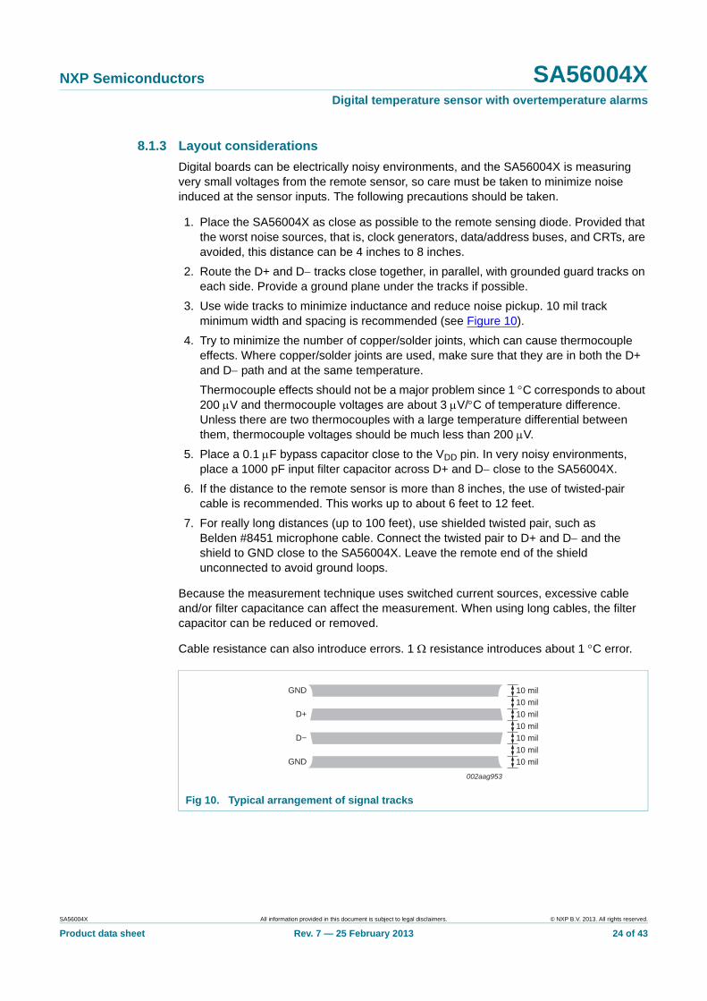
8.1.3 Layout considerations
Digital boards can be electrically noisy environments, and the SA56004X is measuring very small voltages from the remote sensor, so care must be taken to minimize noise induced at the sensor inputs. The following precautions should be taken.
1. Place the SA56004X as close as possible to the remote sensing diode. Provided that the worst noise sources, that is, clock generators, data/address buses, and CRTs, are avoided, this distance can be 4 inches to 8 inches.
2. Route the D+ and D tracks close together, in parallel, with grounded guard tracks on each side. Provide a ground plane under the tracks if possible.
3. Use wide tracks to minimize inductance and reduce noise pickup. 10 mil track minimum width and spacing is recommended (see Figure 10).
4. Try to minimize the number of copper/solder joints, which can cause thermocouple effects. Where copper/solder joints are used, make sure that they are in both the D+ and D path and at the same temperature.
Thermocouple effects should not be a major problem since 1 C corresponds to about 200 V and thermocouple voltages are about 3 V/C of temperature difference. Unless there are two thermocouples with a large temperature differential between them, thermocouple voltages should be much less than 200 V.
5. Place a 0.1 F bypass capacitor close to the VDD pin. In very noisy environments, place a 1000 pF input filter capacitor across D+ and D close to the SA56004X.
6. If the distance to the remote sensor is more than 8 inches, the use of twisted-pair cable is recommended. This works up to about 6 feet to 12 feet.
7. For really long distances (up to 100 feet), use shielded twisted pair, such as Belden #8451 microphone cable. Connect the twisted pair to D+ and D and the shield to GND close to the SA56004X. Leave the remote end of the shield unconnected to avoid ground loops.
Because the measurement technique uses switched current sources, excessive cable and/or filter capacitance can affect the measurement. When using long cables, the filter capacitor can be reduced or removed.
Cable resistance can also introduce errors. 1 resistance introduces about 1 C error.
Fig 10. Typical arrangement of signal tracks
002aag953
GND
GND
D+
D−
10 mil10 mil10 mil10 mil10 mil10 mil10 mil
SA56004X All information provided in this document is subject to legal disclaimers. © NXP B.V. 2013. All rights reserved.
Product data sheet Rev. 7 — 25 February 2013 24 of 43
NXP Semiconductors SA56004XDigital temperature sensor with overtemperature alarms
8.2 Power sequencing considerations
8.2.1 Power supply slew rate
When powering-up the SA56004X, ensure that the slew rate of VDD is less than 18 mV/s. A slew rate larger than this may cause power-on reset issues and yield unpredictable results.
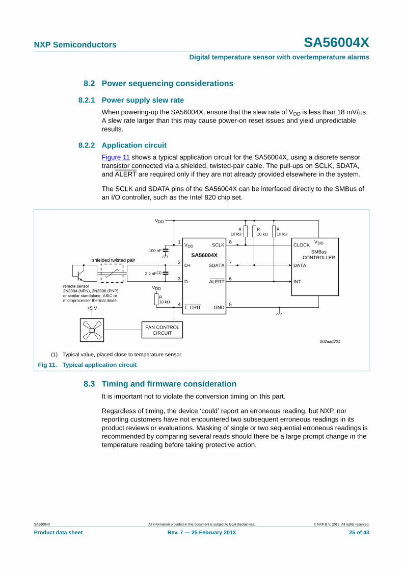
8.2.2 Application circuit
Figure 11 shows a typical application circuit for the SA56004X, using a discrete sensor transistor connected via a shielded, twisted-pair cable. The pull-ups on SCLK, SDATA, and ALERT are required only if they are not already provided elsewhere in the system.
The SCLK and SDATA pins of the SA56004X can be interfaced directly to the SMBus of an I/O controller, such as the Intel 820 chip set.
8.3 Timing and firmware consideration
It is important not to violate the conversion timing on this part.
Regardless of timing, the device ‘could’ report an erroneous reading, but NXP, nor reporting customers have not encountered two subsequent erroneous readings in its product reviews or evaluations. Masking of single or two sequential erroneous readings is recommended by comparing several reads should there be a large prompt change in the temperature reading before taking protective action.
(1) Typical value, placed close to temperature sensor.
Fig 11. Typical application circuit
VDD SCLK
D+ SDATA
D− ALERT
T_CRIT GND
SA56004X
002aad201
1
2
3
4
6
5
8
7shielded twisted pair
100 nF
2.2 nF(1)
VDD
VDD
FAN CONTROLCIRCUIT
+5 V
remote sensor2N3904 (NPN), 2N3906 (PNP), or similar standalone, ASIC or microprocessor thermal diode
R10 kΩ
R10 kΩ
R10 kΩ
R10 kΩ
VDDCLOCK
DATA
INT
SMBusCONTROLLER
SA56004X All information provided in this document is subject to legal disclaimers. © NXP B.V. 2013. All rights reserved.
Product data sheet Rev. 7 — 25 February 2013 25 of 43
NXP Semiconductors SA56004XDigital temperature sensor with overtemperature alarms
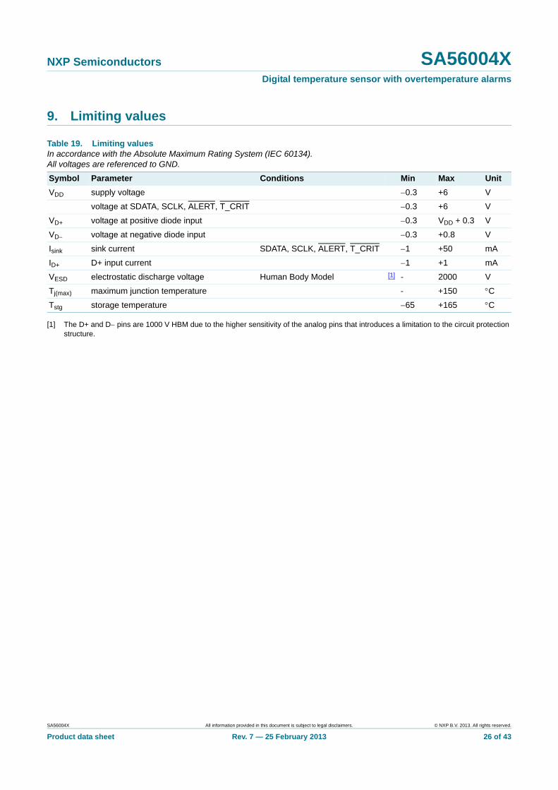
9. Limiting values
[1] The D+ and D pins are 1000 V HBM due to the higher sensitivity of the analog pins that introduces a limitation to the circuit protection structure.
Table 19. Limiting valuesIn accordance with the Absolute Maximum Rating System (IEC 60134).All voltages are referenced to GND.
Symbol Parameter Conditions Min Max Unit
VDD supply voltage 0.3 +6 V
voltage at SDATA, SCLK, ALERT, T_CRIT 0.3 +6 V
VD+ voltage at positive diode input 0.3 VDD + 0.3 V
VD voltage at negative diode input 0.3 +0.8 V
Isink sink current SDATA, SCLK, ALERT, T_CRIT 1 +50 mA
ID+ D+ input current 1 +1 mA
VESD electrostatic discharge voltage Human Body Model [1] - 2000 V
Tj(max) maximum junction temperature - +150 C
Tstg storage temperature 65 +165 C
SA56004X All information provided in this document is subject to legal disclaimers. © NXP B.V. 2013. All rights reserved.
Product data sheet Rev. 7 — 25 February 2013 26 of 43
NXP Semiconductors SA56004XDigital temperature sensor with overtemperature alarms
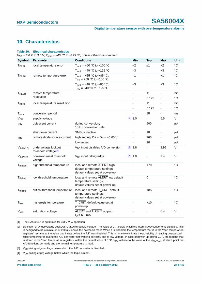
10. Characteristics
[1] The SA56004X is optimized for 3.3 V VDD operation.
[2] Definition of UnderVoltage LockOut (UVLO) threshold voltage: The value of VDD below which the internal A/D converter is disabled. This is designed to be a minimum of 200 mV above the power-on reset. While it is disabled, the temperature that is in the ‘read temperature registers’ remains at the value that it was before the A/D was disabled. This is done to eliminate the possibility of reading unexpected false temperatures due to the A/D converter not working correctly due to low voltage. In case of power-up (rising VDD), the reading that is stored in the ‘read temperature registers’ will be the default value of 0 C. VDD will rise to the value of the Vth(UVLO), at which point the A/D functions correctly and the normal temperature is read.
[3] VDD (rising edge) voltage below which the A/D converter is disabled.
[4] VDD (falling edge) voltage below which the logic is reset.
Table 20. Electrical characteristicsVDD = 3.0 V to 3.6 V; Tamb = 40 C to +125 C; unless otherwise specified.
Symbol Parameter Conditions Min Typ Max Unit
TERRL local temperature error Tamb = +60 C to +100 C 2 1 +2 C
Tamb = 40 C to +125 C 3 - +3 C
TERRR remote temperature error Tamb = +25 C to +85 C; TRD = +60 C to +100 C
1 - +1 C
Tamb = 40 C to +85 C; TRD = 40 C to +125 C
3 - +3 C
TRESR remote temperature resolution
- 11 - bit
- 0.125 - C
TRESL local temperature resolution - 11 - bit
- 0.125 - C
Tconv conversion period - 38 - ms
VDD supply voltage [1] 3.0 - 5.5 V
IDD quiescent current during conversion, 16 Hz conversion rate
- 500 - A
shut-down current SMBus inactive - 10 - A
IRD remote diode source current high setting: D+ D = +0.65 V - 160 - A
low setting - 10 - A
Vth(UVLO) undervoltage lockout threshold voltage[2]
VDD input disables A/D conversion [3] 2.6 - 2.95 V
Vth(POR) power-on reset threshold voltage
VDD input falling edge [4] 1.8 - 2.4 V
Tth(high) high threshold temperature local and remote ALERT high default temperature settings; default values set at power-up
- +70 - C
Tth(low) low threshold temperature local and remote ALERT low default temperature settings; default values set at power-up
- 0 - C
Tth(crit) critical threshold temperature local and remote T_CRIT default temperature settings; default values set at power-up
- +85 - C
Thys hysteresis temperature T_CRIT; default value set at power-up
- +10 - C
Vsat saturation voltage ALERT and T_CRIT output; IO = 6.0 mA
- - 0.4 V
SA56004X All information provided in this document is subject to legal disclaimers. © NXP B.V. 2013. All rights reserved.
Product data sheet Rev. 7 — 25 February 2013 27 of 43
NXP Semiconductors SA56004XDigital temperature sensor with overtemperature alarms
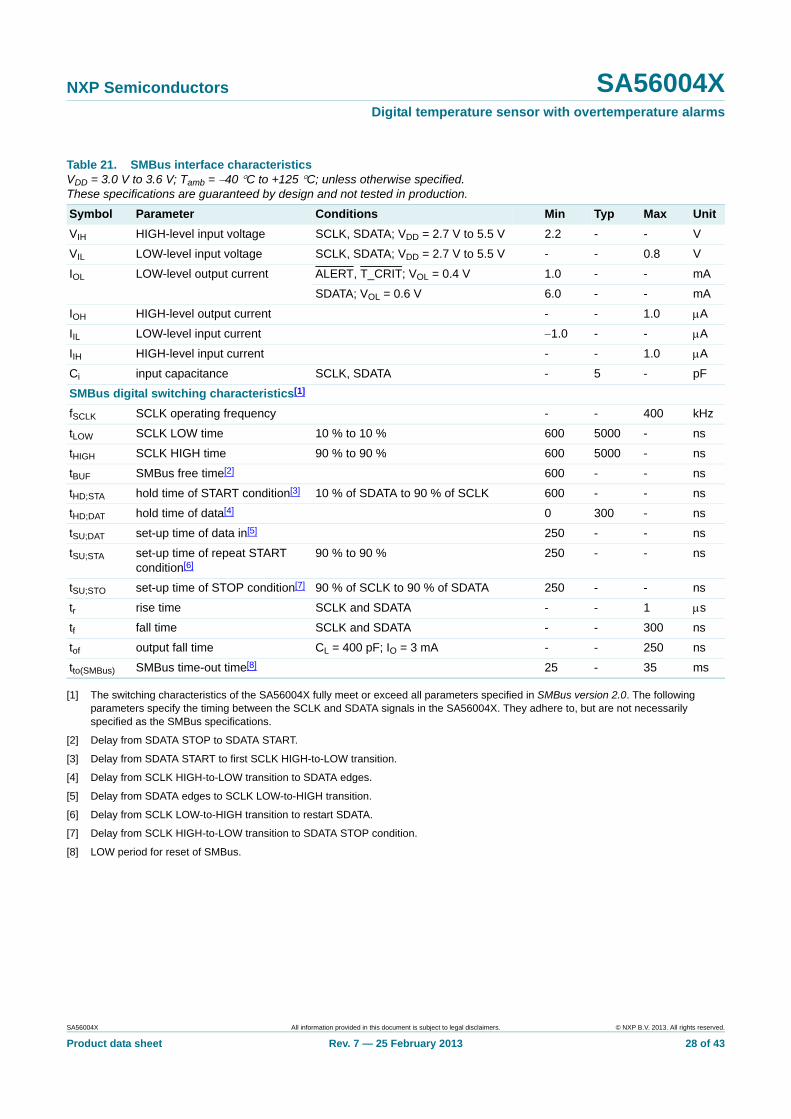
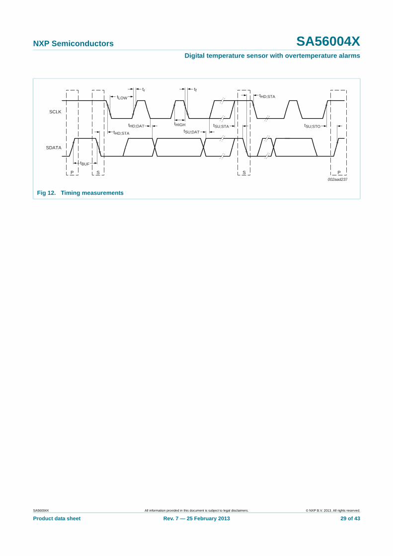
[1] The switching characteristics of the SA56004X fully meet or exceed all parameters specified in SMBus version 2.0. The following parameters specify the timing between the SCLK and SDATA signals in the SA56004X. They adhere to, but are not necessarily specified as the SMBus specifications.
[2] Delay from SDATA STOP to SDATA START.
[3] Delay from SDATA START to first SCLK HIGH-to-LOW transition.
[4] Delay from SCLK HIGH-to-LOW transition to SDATA edges.
[5] Delay from SDATA edges to SCLK LOW-to-HIGH transition.
[6] Delay from SCLK LOW-to-HIGH transition to restart SDATA.
[7] Delay from SCLK HIGH-to-LOW transition to SDATA STOP condition.
[8] LOW period for reset of SMBus.
Table 21. SMBus interface characteristicsVDD = 3.0 V to 3.6 V; Tamb = 40 C to +125 C; unless otherwise specified.These specifications are guaranteed by design and not tested in production.
Symbol Parameter Conditions Min Typ Max Unit
VIH HIGH-level input voltage SCLK, SDATA; VDD = 2.7 V to 5.5 V 2.2 - - V
VIL LOW-level input voltage SCLK, SDATA; VDD = 2.7 V to 5.5 V - - 0.8 V
IOL LOW-level output current ALERT, T_CRIT; VOL = 0.4 V 1.0 - - mA
SDATA; VOL = 0.6 V 6.0 - - mA
IOH HIGH-level output current - - 1.0 A
IIL LOW-level input current 1.0 - - A
IIH HIGH-level input current - - 1.0 A
Ci input capacitance SCLK, SDATA - 5 - pF
SMBus digital switching characteristics[1]
fSCLK SCLK operating frequency - - 400 kHz
tLOW SCLK LOW time 10 % to 10 % 600 5000 - ns
tHIGH SCLK HIGH time 90 % to 90 % 600 5000 - ns
tBUF SMBus free time[2] 600 - - ns
tHD;STA hold time of START condition[3] 10 % of SDATA to 90 % of SCLK 600 - - ns
tHD;DAT hold time of data[4] 0 300 - ns
tSU;DAT set-up time of data in[5] 250 - - ns
tSU;STA set-up time of repeat START condition[6]
90 % to 90 % 250 - - ns
tSU;STO set-up time of STOP condition[7] 90 % of SCLK to 90 % of SDATA 250 - - ns
tr rise time SCLK and SDATA - - 1 s
tf fall time SCLK and SDATA - - 300 ns
tof output fall time CL = 400 pF; IO = 3 mA - - 250 ns
tto(SMBus) SMBus time-out time[8] 25 - 35 ms
SA56004X All information provided in this document is subject to legal disclaimers. © NXP B.V. 2013. All rights reserved.
Product data sheet Rev. 7 — 25 February 2013 28 of 43
NXP Semiconductors SA56004XDigital temperature sensor with overtemperature alarms
Fig 12. Timing measurements
tBUF
tHD;STA
PP S
tLOW
tr
tHD;DAT
tf
tHIGH
tSU;DAT
S
tSU;STO
SDATA
SCLK
tSU;STA
tHD;STA
002aad237
SA56004X All information provided in this document is subject to legal disclaimers. © NXP B.V. 2013. All rights reserved.
Product data sheet Rev. 7 — 25 February 2013 29 of 43
NXP Semiconductors SA56004XDigital temperature sensor with overtemperature alarms
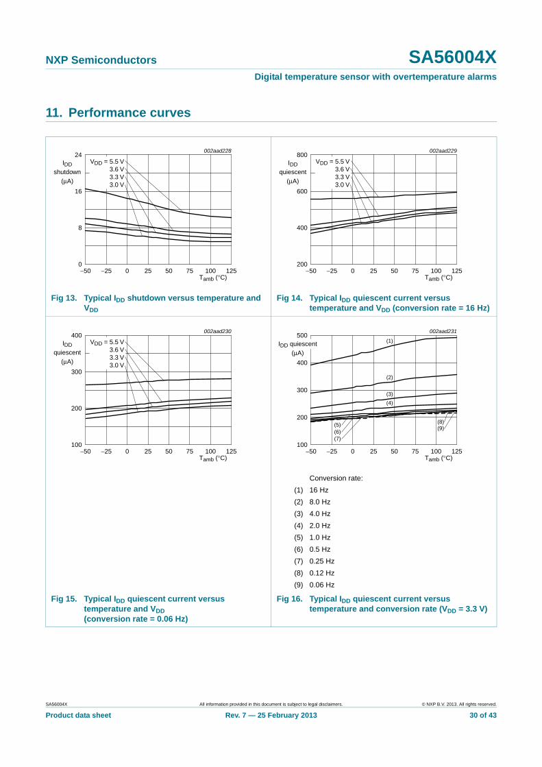
11. Performance curves
Fig 13. Typical IDD shutdown versus temperature and VDD
Fig 14. Typical IDD quiescent current versus temperature and VDD (conversion rate = 16 Hz)
Conversion rate:
(1) 16 Hz
(2) 8.0 Hz
(3) 4.0 Hz
(4) 2.0 Hz
(5) 1.0 Hz
(6) 0.5 Hz
(7) 0.25 Hz
(8) 0.12 Hz
(9) 0.06 Hz
Fig 15. Typical IDD quiescent current versus temperature and VDD (conversion rate = 0.06 Hz)
Fig 16. Typical IDD quiescent current versus temperature and conversion rate (VDD = 3.3 V)
8
16
24IDD
shutdown(μA)
0
Tamb (°C)−50 125
002aad228
1007550250−25
VDD = 5.5 V3.6 V3.3 V3.0 V
400
600
800IDD
quiescent(μA)
200
Tamb (°C)−50 125
002aad229
1007550250−25
VDD = 5.5 V3.6 V3.3 V3.0 V
200
300
400IDD
quiescent(μA)
100
Tamb (°C)−50 125
002aad230
1007550250−25
VDD = 5.5 V3.6 V3.3 V3.0 V
500
100
Tamb (°C)−50 125
002aad231
1007550250−25
200
300
400
IDD quiescent(μA)
(1)
(2)
(3)
(4)
(5)(6)(7)
(8)(9)
SA56004X All information provided in this document is subject to legal disclaimers. © NXP B.V. 2013. All rights reserved.
Product data sheet Rev. 7 — 25 February 2013 30 of 43
NXP Semiconductors SA56004XDigital temperature sensor with overtemperature alarms
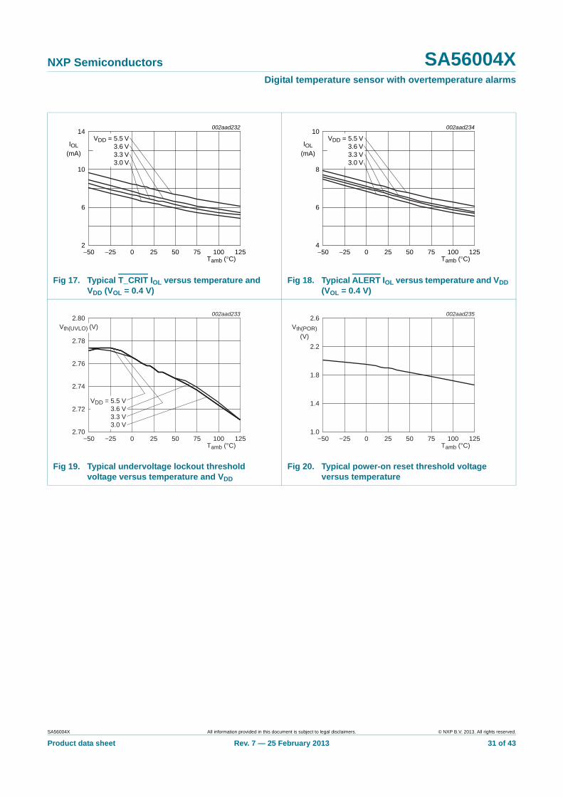
Fig 17. Typical T_CRIT IOL versus temperature and VDD (VOL = 0.4 V)
Fig 18. Typical ALERT IOL versus temperature and VDD (VOL = 0.4 V)
Fig 19. Typical undervoltage lockout threshold voltage versus temperature and VDD
Fig 20. Typical power-on reset threshold voltage versus temperature
6
10
14
IOL(mA)
2
Tamb (°C)−50 125
002aad232
1007550250−25
VDD = 5.5 V3.6 V3.3 V3.0 V
6
8
10
IOL(mA)
4
Tamb (°C)−50 125
002aad234
1007550250−25
VDD = 5.5 V3.6 V3.3 V3.0 V
Tamb (°C)−50 125
002aad233
1007550250−25
VDD = 5.5 V3.6 V3.3 V3.0 V
2.78
2.74
2.72
2.76
2.80
2.70
Vth(UVLO) (V)2.6
1.0
Tamb (°C)−50 125
002aad235
1007550250−25
1.4
1.8
2.2
Vth(POR)(V)
SA56004X All information provided in this document is subject to legal disclaimers. © NXP B.V. 2013. All rights reserved.
Product data sheet Rev. 7 — 25 February 2013 31 of 43
NXP Semiconductors SA56004XDigital temperature sensor with overtemperature alarms
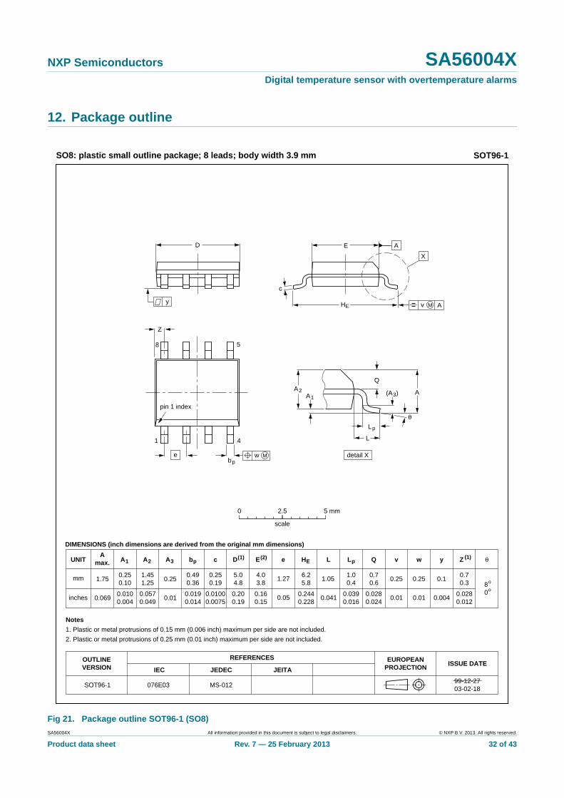
12. Package outline
Fig 21. Package outline SOT96-1 (SO8)
UNITA
max. A1 A2 A3 bp c D(1) E(2) (1)e HE L Lp Q Zywv θ
REFERENCESOUTLINEVERSION
EUROPEANPROJECTION ISSUE DATE
IEC JEDEC JEITA
mm
inches
1.750.250.10
1.451.25
0.250.490.36
0.250.19
5.04.8
4.03.8
1.276.25.8
1.050.70.6
0.70.3 8
0
o
o
0.25 0.10.25
DIMENSIONS (inch dimensions are derived from the original mm dimensions)
Notes
1. Plastic or metal protrusions of 0.15 mm (0.006 inch) maximum per side are not included.
2. Plastic or metal protrusions of 0.25 mm (0.01 inch) maximum per side are not included.
1.00.4
SOT96-1
X
w M
θ
AA1
A2
bp
D
HE
Lp
Q
detail X
E
Z
e
c
L
v M A
(A )3
A
4
5
pin 1 index
1
8
y
076E03 MS-012
0.0690.0100.004
0.0570.049
0.010.0190.014
0.01000.0075
0.200.19
0.160.15
0.050.2440.228
0.0280.024
0.0280.012
0.010.010.041 0.0040.0390.016
0 2.5 5 mm
scale
SO8: plastic small outline package; 8 leads; body width 3.9 mm SOT96-1
99-12-2703-02-18
SA56004X All information provided in this document is subject to legal disclaimers. © NXP B.V. 2013. All rights reserved.
Product data sheet Rev. 7 — 25 February 2013 32 of 43
NXP Semiconductors SA56004XDigital temperature sensor with overtemperature alarms
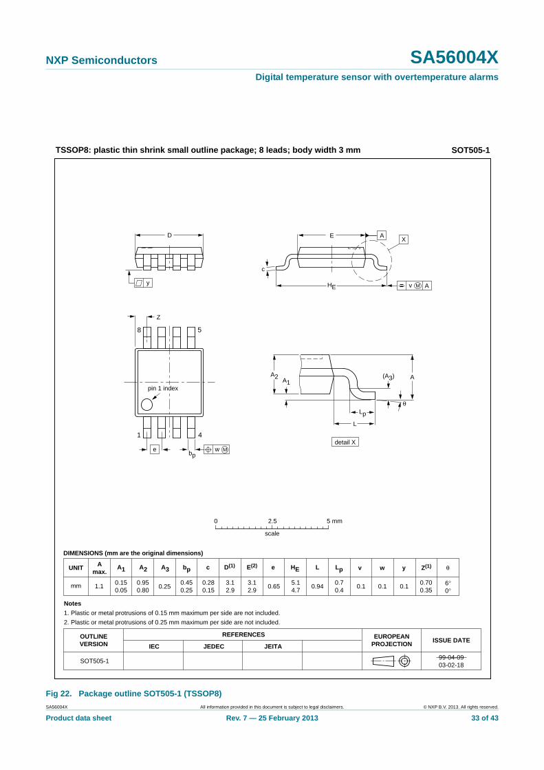
Fig 22. Package outline SOT505-1 (TSSOP8)
UNIT A1A
max.A2 A3 bp LHE Lp w yvc eD(1) E(2) Z(1) θ
REFERENCESOUTLINEVERSION
EUROPEANPROJECTION ISSUE DATE
IEC JEDEC JEITA
mm 0.150.05
0.950.80
0.450.25
0.280.15
3.12.9
3.12.9
0.655.14.7
0.700.35
6°0°
0.1 0.10.10.94
DIMENSIONS (mm are the original dimensions)
Notes
1. Plastic or metal protrusions of 0.15 mm maximum per side are not included.
2. Plastic or metal protrusions of 0.25 mm maximum per side are not included.
0.70.4
SOT505-1 99-04-0903-02-18
w Mbp
D
Z
e
0.25
1 4
8 5
θ
AA2A1
Lp
(A3)
detail X
L
HE
E
c
v M A
XA
y
2.5 5 mm0
scale
TSSOP8: plastic thin shrink small outline package; 8 leads; body width 3 mm SOT505-1
1.1
pin 1 index
SA56004X All information provided in this document is subject to legal disclaimers. © NXP B.V. 2013. All rights reserved.
Product data sheet Rev. 7 — 25 February 2013 33 of 43
NXP Semiconductors SA56004XDigital temperature sensor with overtemperature alarms
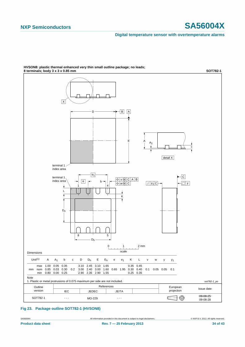
Fig 23. Package outline SOT782-1 (HVSON8)
ReferencesOutlineversion
Europeanprojection
Issue dateIEC JEDEC JEITA
SOT782-1 - - -- - -
sot782-1_po
09-08-2509-08-28
Unit(1)
mmmaxnommin
1.000.850.80
0.050.030.00
0.23.103.002.90
2.452.402.35
3.103.002.90
0.65 1.950.450.400.35
0.1
A
Dimensions
Note1. Plastic or metal protrusions of 0.075 maximum per side are not included.
HVSON8: plastic thermal enhanced very thin small outline package; no leads;8 terminals; body 3 x 3 x 0.85 mm SOT782-1
A1 b
0.350.300.25
c D Dh E Eh
1.651.601.55
e e1 K
0.350.300.25
L v
0.1
w
0.05
y
0.05
y1
0 1 2 mm
scale
MO-229
X
C
yCy1
detail X
A
cA1
B AD
E
terminal 1index area
b
Dh
L
Eh
K
e1
eAC Bv
Cw1 4
8 5
terminal 1index area
SA56004X All information provided in this document is subject to legal disclaimers. © NXP B.V. 2013. All rights reserved.
Product data sheet Rev. 7 — 25 February 2013 34 of 43
NXP Semiconductors SA56004XDigital temperature sensor with overtemperature alarms
13. Soldering of SMD packages
This text provides a very brief insight into a complex technology. A more in-depth account of soldering ICs can be found in Application Note AN10365 “Surface mount reflow soldering description”.
13.1 Introduction to soldering
Soldering is one of the most common methods through which packages are attached to Printed Circuit Boards (PCBs), to form electrical circuits. The soldered joint provides both the mechanical and the electrical connection. There is no single soldering method that is ideal for all IC packages. Wave soldering is often preferred when through-hole and Surface Mount Devices (SMDs) are mixed on one printed wiring board; however, it is not suitable for fine pitch SMDs. Reflow soldering is ideal for the small pitches and high densities that come with increased miniaturization.
13.2 Wave and reflow soldering
Wave soldering is a joining technology in which the joints are made by solder coming from a standing wave of liquid solder. The wave soldering process is suitable for the following:
• Through-hole components
• Leaded or leadless SMDs, which are glued to the surface of the printed circuit board
Not all SMDs can be wave soldered. Packages with solder balls, and some leadless packages which have solder lands underneath the body, cannot be wave soldered. Also, leaded SMDs with leads having a pitch smaller than ~0.6 mm cannot be wave soldered, due to an increased probability of bridging.
The reflow soldering process involves applying solder paste to a board, followed by component placement and exposure to a temperature profile. Leaded packages, packages with solder balls, and leadless packages are all reflow solderable.
Key characteristics in both wave and reflow soldering are:
• Board specifications, including the board finish, solder masks and vias
• Package footprints, including solder thieves and orientation
• The moisture sensitivity level of the packages
• Package placement
• Inspection and repair
• Lead-free soldering versus SnPb soldering
13.3 Wave soldering
Key characteristics in wave soldering are:
• Process issues, such as application of adhesive and flux, clinching of leads, board transport, the solder wave parameters, and the time during which components are exposed to the wave
• Solder bath specifications, including temperature and impurities
SA56004X All information provided in this document is subject to legal disclaimers. © NXP B.V. 2013. All rights reserved.
Product data sheet Rev. 7 — 25 February 2013 35 of 43

NXP Semiconductors SA56004XDigital temperature sensor with overtemperature alarms
13.4 Reflow soldering
Key characteristics in reflow soldering are:
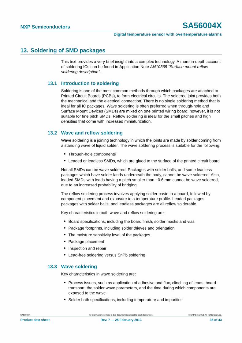
• Lead-free versus SnPb soldering; note that a lead-free reflow process usually leads to higher minimum peak temperatures (see Figure 24) than a SnPb process, thus reducing the process window
• Solder paste printing issues including smearing, release, and adjusting the process window for a mix of large and small components on one board
• Reflow temperature profile; this profile includes preheat, reflow (in which the board is heated to the peak temperature) and cooling down. It is imperative that the peak temperature is high enough for the solder to make reliable solder joints (a solder paste characteristic). In addition, the peak temperature must be low enough that the packages and/or boards are not damaged. The peak temperature of the package depends on package thickness and volume and is classified in accordance with Table 22 and 23
Moisture sensitivity precautions, as indicated on the packing, must be respected at all times.
Studies have shown that small packages reach higher temperatures during reflow soldering, see Figure 24.
Table 22. SnPb eutectic process (from J-STD-020C)
Package thickness (mm) Package reflow temperature (C)
Volume (mm3)
< 350 350
< 2.5 235 220
2.5 220 220
Table 23. Lead-free process (from J-STD-020C)
Package thickness (mm) Package reflow temperature (C)
Volume (mm3)
< 350 350 to 2000 > 2000
< 1.6 260 260 260
1.6 to 2.5 260 250 245
> 2.5 250 245 245
SA56004X All information provided in this document is subject to legal disclaimers. © NXP B.V. 2013. All rights reserved.
Product data sheet Rev. 7 — 25 February 2013 36 of 43
NXP Semiconductors SA56004XDigital temperature sensor with overtemperature alarms
For further information on temperature profiles, refer to Application Note AN10365 “Surface mount reflow soldering description”.
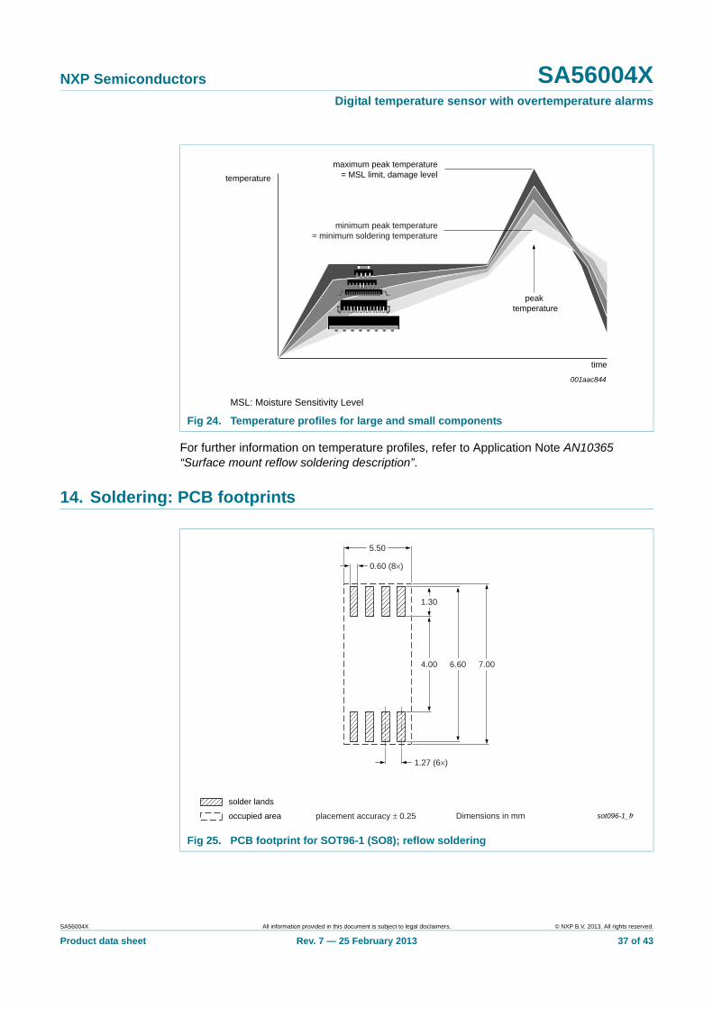
14. Soldering: PCB footprints
MSL: Moisture Sensitivity Level
Fig 24. Temperature profiles for large and small components
001aac844
temperature
time
minimum peak temperature= minimum soldering temperature
maximum peak temperature= MSL limit, damage level
peak temperature
Fig 25. PCB footprint for SOT96-1 (SO8); reflow soldering
sot096-1_froccupied area
solder lands
Dimensions in mmplacement accuracy ± 0.25
1.30
0.60 (8×)
1.27 (6×)
4.00 6.60
5.50
7.00
SA56004X All information provided in this document is subject to legal disclaimers. © NXP B.V. 2013. All rights reserved.
Product data sheet Rev. 7 — 25 February 2013 37 of 43

NXP Semiconductors SA56004XDigital temperature sensor with overtemperature alarms
Fig 26. PCB footprint for SOT96-1 (SO8); wave soldering
Fig 27. PCB footprint for SOT505-1 (TSSOP8); reflow soldering
sot096-1_fw
solder resist
occupied area
solder lands
Dimensions in mm
board direction
placement accurracy ± 0.25
4.00
5.50
1.30
0.3 (2×)0.60 (6×)
1.20 (2×)
1.27 (6×)
7.006.60
enlarged solder land
sot505-1_froccupied areasolder lands Dimensions in mm
3.2003.6005.750
0.725
0.650
0.125
0.4500.600
3.600
2.950
0.125
1.150
5.500
SA56004X All information provided in this document is subject to legal disclaimers. © NXP B.V. 2013. All rights reserved.
Product data sheet Rev. 7 — 25 February 2013 38 of 43

NXP Semiconductors SA56004XDigital temperature sensor with overtemperature alarms
Fig 28. PCB footprint for SOT782-1 (HVSON8); reflow soldering
SOT782-1
DIMENSIONS in mm
Footprint information for reflow soldering of HVSON8 package
Ay By D SLx SLy SPx SPy Gx Gy
3.25 2.2
P
0.65 0.3
C
0.525 2.45 1.65 1.1 0.65 3.25 3.25
Hy
3.5
nSPx nSPy
1 1
occupied area
solder land plus solder paste
solder land
solder paste deposit
sot782-1_frIssue date 12-02-0912-02-28
GyHy
C
SLx
AyBySLy
Gx
DP
nSPx
nSPy
SPy
SPx
SA56004X All information provided in this document is subject to legal disclaimers. © NXP B.V. 2013. All rights reserved.
Product data sheet Rev. 7 — 25 February 2013 39 of 43

NXP Semiconductors SA56004XDigital temperature sensor with overtemperature alarms
15. Abbreviations
16. Revision history
Table 24. Abbreviations
Acronym Description
A/D Analog-to-Digital
ARA Alert Response Address
ASIC Application Specific Integrated Circuit
CRT Cathode Ray Tube
ESD ElectroStatic Discharge
HBM Human Body Model
HVAC Heating, Ventilating and Air Conditioning
I2C-bus Inter-Integrated Circuit bus
LSB Least Significant Bit
MSB Most Significant Bit
OTP One-Time Programmable
POR Power-On Reset
PTAT Proportional To Absolute Temperature
SMBus System Management Bus
UVLO Under Voltage LockOut
Table 25. Revision history
Document ID Release date Data sheet status Change notice Supersedes
SA56004X v.7 20130225 Product data sheet - SA56004X v.6
Modifications: • Table 1 “Ordering information”: added “Topside marking” column and corrected Topside marking for SO8 package (appended “D”)
• Table 2 “Ordering options” modified:
– deleted column “Topside marking” (moved to Table 1)
– added columns “Orderable part number”, “Package”, “Packing method”, “Minimum order quantity”
• Section 7.2 “Slave address”: added (new) Table 4 “Slave addresses”
• Added (new) Section 8.3 “Timing and firmware consideration”
• Deleted (old) Section 13 “Packing information”
• Added (new) Section 14 “Soldering: PCB footprints”
SA56004X v.6 20120423 Product data sheet - SA56004X v.5
SA56004X v.5 20080522 Product data sheet - SA56004X v.4
SA56004X v.4 20060808 Product data sheet - SA56004X v.3
SA56004X v.3 (9397 750 13841)
20041006 Product data sheet - SA56004X v.2
SA56004X v.2 (9397 750 12015)
20030903 Objective data - SA56004-X v.1
SA56004-X v.1 (9397 750 10993)
20030819 Objective data - -
SA56004X All information provided in this document is subject to legal disclaimers. © NXP B.V. 2013. All rights reserved.
Product data sheet Rev. 7 — 25 February 2013 40 of 43

NXP Semiconductors SA56004XDigital temperature sensor with overtemperature alarms
17. Legal information
17.1 Data sheet status
[1] Please consult the most recently issued document before initiating or completing a design.
[2] The term ‘short data sheet’ is explained in section “Definitions”.
[3] The product status of device(s) described in this document may have changed since this document was published and may differ in case of multiple devices. The latest product status information is available on the Internet at URL http://www.nxp.com.
17.2 Definitions
Draft — The document is a draft version only. The content is still under internal review and subject to formal approval, which may result in modifications or additions. NXP Semiconductors does not give any representations or warranties as to the accuracy or completeness of information included herein and shall have no liability for the consequences of use of such information.
Short data sheet — A short data sheet is an extract from a full data sheet with the same product type number(s) and title. A short data sheet is intended for quick reference only and should not be relied upon to contain detailed and full information. For detailed and full information see the relevant full data sheet, which is available on request via the local NXP Semiconductors sales office. In case of any inconsistency or conflict with the short data sheet, the full data sheet shall prevail.
Product specification — The information and data provided in a Product data sheet shall define the specification of the product as agreed between NXP Semiconductors and its customer, unless NXP Semiconductors and customer have explicitly agreed otherwise in writing. In no event however, shall an agreement be valid in which the NXP Semiconductors product is deemed to offer functions and qualities beyond those described in the Product data sheet.
17.3 Disclaimers
Limited warranty and liability — Information in this document is believed to be accurate and reliable. However, NXP Semiconductors does not give any representations or warranties, expressed or implied, as to the accuracy or completeness of such information and shall have no liability for the consequences of use of such information. NXP Semiconductors takes no responsibility for the content in this document if provided by an information source outside of NXP Semiconductors.
In no event shall NXP Semiconductors be liable for any indirect, incidental, punitive, special or consequential damages (including - without limitation - lost profits, lost savings, business interruption, costs related to the removal or replacement of any products or rework charges) whether or not such damages are based on tort (including negligence), warranty, breach of contract or any other legal theory.
Notwithstanding any damages that customer might incur for any reason whatsoever, NXP Semiconductors’ aggregate and cumulative liability towards customer for the products described herein shall be limited in accordance with the Terms and conditions of commercial sale of NXP Semiconductors.
Right to make changes — NXP Semiconductors reserves the right to make changes to information published in this document, including without limitation specifications and product descriptions, at any time and without notice. This document supersedes and replaces all information supplied prior to the publication hereof.
Suitability for use — NXP Semiconductors products are not designed, authorized or warranted to be suitable for use in life support, life-critical or safety-critical systems or equipment, nor in applications where failure or malfunction of an NXP Semiconductors product can reasonably be expected to result in personal injury, death or severe property or environmental damage. NXP Semiconductors and its suppliers accept no liability for inclusion and/or use of NXP Semiconductors products in such equipment or applications and therefore such inclusion and/or use is at the customer’s own risk.
Applications — Applications that are described herein for any of these products are for illustrative purposes only. NXP Semiconductors makes no representation or warranty that such applications will be suitable for the specified use without further testing or modification.
Customers are responsible for the design and operation of their applications and products using NXP Semiconductors products, and NXP Semiconductors accepts no liability for any assistance with applications or customer product design. It is customer’s sole responsibility to determine whether the NXP Semiconductors product is suitable and fit for the customer’s applications and products planned, as well as for the planned application and use of customer’s third party customer(s). Customers should provide appropriate design and operating safeguards to minimize the risks associated with their applications and products.
NXP Semiconductors does not accept any liability related to any default, damage, costs or problem which is based on any weakness or default in the customer’s applications or products, or the application or use by customer’s third party customer(s). Customer is responsible for doing all necessary testing for the customer’s applications and products using NXP Semiconductors products in order to avoid a default of the applications and the products or of the application or use by customer’s third party customer(s). NXP does not accept any liability in this respect.
Limiting values — Stress above one or more limiting values (as defined in the Absolute Maximum Ratings System of IEC 60134) will cause permanent damage to the device. Limiting values are stress ratings only and (proper) operation of the device at these or any other conditions above those given in the Recommended operating conditions section (if present) or the Characteristics sections of this document is not warranted. Constant or repeated exposure to limiting values will permanently and irreversibly affect the quality and reliability of the device.
Terms and conditions of commercial sale — NXP Semiconductors products are sold subject to the general terms and conditions of commercial sale, as published at http://www.nxp.com/profile/terms, unless otherwise agreed in a valid written individual agreement. In case an individual agreement is concluded only the terms and conditions of the respective agreement shall apply. NXP Semiconductors hereby expressly objects to applying the customer’s general terms and conditions with regard to the purchase of NXP Semiconductors products by customer.
No offer to sell or license — Nothing in this document may be interpreted or construed as an offer to sell products that is open for acceptance or the grant, conveyance or implication of any license under any copyrights, patents or other industrial or intellectual property rights.
Document status[1][2] Product status[3] Definition
Objective [short] data sheet Development This document contains data from the objective specification for product development.
Preliminary [short] data sheet Qualification This document contains data from the preliminary specification.
Product [short] data sheet Production This document contains the product specification.
SA56004X All information provided in this document is subject to legal disclaimers. © NXP B.V. 2013. All rights reserved.
Product data sheet Rev. 7 — 25 February 2013 41 of 43
NXP Semiconductors SA56004XDigital temperature sensor with overtemperature alarms
Export control — This document as well as the item(s) described herein may be subject to export control regulations. Export might require a prior authorization from competent authorities.
Non-automotive qualified products — Unless this data sheet expressly states that this specific NXP Semiconductors product is automotive qualified, the product is not suitable for automotive use. It is neither qualified nor tested in accordance with automotive testing or application requirements. NXP Semiconductors accepts no liability for inclusion and/or use of non-automotive qualified products in automotive equipment or applications.
In the event that customer uses the product for design-in and use in automotive applications to automotive specifications and standards, customer (a) shall use the product without NXP Semiconductors’ warranty of the product for such automotive applications, use and specifications, and (b) whenever customer uses the product for automotive applications beyond NXP Semiconductors’ specifications such use shall be solely at customer’s
own risk, and (c) customer fully indemnifies NXP Semiconductors for any liability, damages or failed product claims resulting from customer design and use of the product for automotive applications beyond NXP Semiconductors’ standard warranty and NXP Semiconductors’ product specifications.
Translations — A non-English (translated) version of a document is for reference only. The English version shall prevail in case of any discrepancy between the translated and English versions.
17.4 TrademarksNotice: All referenced brands, product names, service names and trademarks are the property of their respective owners.
I2C-bus — logo is a trademark of NXP B.V.
18. Contact information
For more information, please visit: http://www.nxp.com
For sales office addresses, please send an email to: [email protected]
SA56004X All information provided in this document is subject to legal disclaimers. © NXP B.V. 2013. All rights reserved.
Product data sheet Rev. 7 — 25 February 2013 42 of 43

NXP Semiconductors SA56004XDigital temperature sensor with overtemperature alarms
19. Contents
1 General description . . . . . . . . . . . . . . . . . . . . . . 1
2 Features and benefits . . . . . . . . . . . . . . . . . . . . 1
3 Applications . . . . . . . . . . . . . . . . . . . . . . . . . . . . 2
4 Ordering information. . . . . . . . . . . . . . . . . . . . . 24.1 Ordering options . . . . . . . . . . . . . . . . . . . . . . . . 3
5 Block diagram . . . . . . . . . . . . . . . . . . . . . . . . . . 4
6 Pinning information. . . . . . . . . . . . . . . . . . . . . . 56.1 Pinning . . . . . . . . . . . . . . . . . . . . . . . . . . . . . . . 56.2 Pin description . . . . . . . . . . . . . . . . . . . . . . . . . 5
7 Functional description . . . . . . . . . . . . . . . . . . . 67.1 Serial bus interface. . . . . . . . . . . . . . . . . . . . . . 67.2 Slave address. . . . . . . . . . . . . . . . . . . . . . . . . . 67.3 Register overview . . . . . . . . . . . . . . . . . . . . . . . 77.4 Power-on reset . . . . . . . . . . . . . . . . . . . . . . . . . 87.5 Starting conversion . . . . . . . . . . . . . . . . . . . . . . 97.6 Low power software standby mode . . . . . . . . . 97.7 Temperature data format . . . . . . . . . . . . . . . . . 97.8 SA56004X SMBus registers . . . . . . . . . . . . . . 107.8.1 Command register . . . . . . . . . . . . . . . . . . . . . 107.8.2 Local and remote temperature registers
(LTHB, LTLB, RTHB, RTLB) . . . . . . . . . . . . . . 107.8.3 Configuration register (CON) . . . . . . . . . . . . . 107.8.4 Status register (SR) . . . . . . . . . . . . . . . . . . . . 117.8.5 Conversion rate register (CR). . . . . . . . . . . . . 127.8.6 Temperature limit registers . . . . . . . . . . . . . . . 127.8.7 Programmable offset register (remote only) . . 137.8.8 ALERT mode register (AM) . . . . . . . . . . . . . . 137.8.9 Other registers . . . . . . . . . . . . . . . . . . . . . . . . 137.8.10 One-shot register . . . . . . . . . . . . . . . . . . . . . . 137.9 Interruption logic and functional description . . 147.9.1 ALERT output . . . . . . . . . . . . . . . . . . . . . . . . . 147.9.1.1 ALERT output in comparator mode . . . . . . . . 147.9.1.2 ALERT output in interrupt mode . . . . . . . . . . . 147.9.1.3 ALERT output in SMBus ALERT mode . . . . . 157.9.2 T_CRIT output . . . . . . . . . . . . . . . . . . . . . . . . 177.9.3 Fault Queue . . . . . . . . . . . . . . . . . . . . . . . . . . 187.9.4 Temperature measurement . . . . . . . . . . . . . . 197.9.5 Diode fault detection. . . . . . . . . . . . . . . . . . . . 197.10 SMBus interface . . . . . . . . . . . . . . . . . . . . . . . 207.10.1 Serial interface reset. . . . . . . . . . . . . . . . . . . . 22
8 Application design-in information . . . . . . . . . 228.1 Factors affecting accuracy . . . . . . . . . . . . . . . 228.1.1 Remote sensing diode . . . . . . . . . . . . . . . . . . 228.1.2 Thermal inertia and self-heating . . . . . . . . . . . 238.1.3 Layout considerations. . . . . . . . . . . . . . . . . . . 248.2 Power sequencing considerations . . . . . . . . . 25
8.2.1 Power supply slew rate . . . . . . . . . . . . . . . . . 258.2.2 Application circuit . . . . . . . . . . . . . . . . . . . . . . 258.3 Timing and firmware consideration . . . . . . . . 25
9 Limiting values . . . . . . . . . . . . . . . . . . . . . . . . 26
10 Characteristics . . . . . . . . . . . . . . . . . . . . . . . . 27
11 Performance curves . . . . . . . . . . . . . . . . . . . . 30
12 Package outline. . . . . . . . . . . . . . . . . . . . . . . . 32
13 Soldering of SMD packages. . . . . . . . . . . . . . 3513.1 Introduction to soldering. . . . . . . . . . . . . . . . . 3513.2 Wave and reflow soldering. . . . . . . . . . . . . . . 3513.3 Wave soldering . . . . . . . . . . . . . . . . . . . . . . . 3513.4 Reflow soldering . . . . . . . . . . . . . . . . . . . . . . 36
14 Soldering: PCB footprints . . . . . . . . . . . . . . . 37
15 Abbreviations . . . . . . . . . . . . . . . . . . . . . . . . . 40
16 Revision history . . . . . . . . . . . . . . . . . . . . . . . 40
17 Legal information . . . . . . . . . . . . . . . . . . . . . . 4117.1 Data sheet status . . . . . . . . . . . . . . . . . . . . . . 4117.2 Definitions . . . . . . . . . . . . . . . . . . . . . . . . . . . 4117.3 Disclaimers . . . . . . . . . . . . . . . . . . . . . . . . . . 4117.4 Trademarks . . . . . . . . . . . . . . . . . . . . . . . . . . 42
18 Contact information . . . . . . . . . . . . . . . . . . . . 42
19 Contents. . . . . . . . . . . . . . . . . . . . . . . . . . . . . . 43
© NXP B.V. 2013. All rights reserved.
For more information, please visit: http://www.nxp.comFor sales office addresses, please send an email to: [email protected]
Date of release: 25 February 2013
Document identifier: SA56004X
Please be aware that important notices concerning this document and the product(s)described herein, have been included in section ‘Legal information’.