s1d15e06 series - rockbox€¦ · 106 com59 1325 107 com58 1275 108 com57 1225 109 com56 1175 110...
TRANSCRIPT

S1D15E06 Series
MF1393-05
Rev. 2.1

NOTICE
No part of this material may be reproduced or duplicated in any from or by any means without the writtenpermission of Seiko Epson. Seiko Epson reserves the right to make changes to this material without notics.Seiko Epson does not assume any liability of any kind arising out of any inaccuracies contained in this materialor due to its application or use in any product or circuit and, further, there is no repersesnation that this material isapplicable to products requiring high level reliability, such as, medical products. Moreover, no license to anyintellectual property rights is granted by implication or otherwise, and there is no representation or warranty thatanything made in accordance with this material will be free from any patent or copyright infringement of a thirdparty. This material or portions thereof may contain technology or the subject relating to strategic productsunder the control of the Foreign Exchange and Foreign Trade Law of Japan and may require an export licensefrom the Ministry of International Trade and Industry or other approval from another government agency.
©SEIKO EPSON CORPORATION 2003, All rights reserved.
All other product names mentioned herein are trademarks and/or registered trademarks of their respectivecompanies.
Rev. 2.1

– i –
SED1575 Series
Rev. 2.1
Contents
1. DESCRIPTION .................................................................................................................................................. 1
2. FEATURES ........................................................................................................................................................ 1
3. BLOCK DIAGRAM ............................................................................................................................................. 2
4. PIN ASSIGNMENT ............................................................................................................................................ 3
5. PIN DESCRIPTION ........................................................................................................................................... 7
6. FUNCTIONAL DESCRIPTION ........................................................................................................................ 11
7. COMMAND ...................................................................................................................................................... 27
8. ABSOLUTE MAXIMUM RATINGS .................................................................................................................. 50
9. DC CHARACTERISTICS................................................................................................................................. 51
10. TIMING CHARACTERISTICS ......................................................................................................................... 58
11. MPU INTERFACE (Reference example) ......................................................................................................... 66
12. CONNECTION BETWEEN LCD DRIVERS (Reference example) .................................................................. 67
13. LCD PANEL WIRING (Reference example) .................................................................................................... 68
14. S1D15E06T00A*** TCP PIN LAYOUT ........................................................................................................ 69
15. TCP DIMENSIONS (Reference example) ....................................................................................................... 70
16. CAUTIONS ...................................................................................................................................................... 71

S1D15E06 Series
Rev. 2.1 EPSON 1
2. FEATURES• Direct RAM data display by display data RAM
• 4 gray-scale display (Normally white in normal display mode)
RAM bit data (high order and low order)(1,1) : gray-scale 3, black(1,0) : gray-scale 2(0,1) : gray-scale 1(0,0) : gray-scale 0, white
• Binary display (Normally white display is in normal mode)
RAM bit data“1” : On and black“0” : Off and white
• RAM capacity132 × 160 × 2 = 42,240 bits
• Liquid crystal drive circuit132 common outputs and 160 segment outputs
• High-speed 8-bit MPU interface (directly connectableto the MPUs of both 80/68 series) /serial interfacepossible
• A variety of command functionsArea scroll display, partial display, n-line reversal,display data RAM address control, contrast control,display ON/OFF, display normal/reverse rotation,display all lighting ON/OFF, liquid crystal drivepower supply circuit control, display clock built-inoscillator circuit control
• Lower power MLS drive technologyBuilt-in high precision voltage regulation function
• High precision CR oscillator circuit incorporated• Very low power consumption• Power supply
Logic power supply: VDD – VSS = 1.7 to 3.6 VLiquid crystal drive power supply:V3 – VSS = 3.4 to 14.0 V (S1D15E06D01****),V3 – VSS = 3.4 to 16.0 V (S1D15E06D03****)
• Wide operation temperature range: –40 to 85°C• CMOS process• Shipping form : Bare chips, TCP• Light and radiation proof measures are not taken in
designing.
1. DESCRIPTIONThe S1D15E06 series is a single chip MLS driver for dotmatrix liquid crystal displays which can be directlyconnected to the microcomputer bus. It accepts the 8-bit parallel or serial display data from the microcomputerto store the data in the on-chip display data RAM, andissues liquid crystal drive signals independently of themicrocomputer.The S1D15E06 series provides both 4 gray-scale displayand binary display. It incorporates a display data RAM(132 × 160 × 2 bits). In the case of 4 gray-scale display,2 bits of the on-chip RAM respond to one-dot pixels,while in the case of binary display, 1 bit of the on-chipRAM respond to one-dot pixels.The S1D15E06 series features 132 common outputcircuits and 160 segment output circuits. A single chipprovides a display of 10 characters by 8 lines with 132× 160 dots (16 × 16 dots) and display of 13 characters by11 lines by the 12 × 12 dot-character font.Display data RAM read/write operations do not requireoperation clock from outside, thereby ensuring operationwith the minimum current consumption. Furthermore,it incorporates a LCD-drive power supply characterizedby low power consumption and a CR oscillator circuitfor display clock; therefore, the display system of ahandy and high-performance instrument can be realizedby use of the minimum current consumption andminimum chip configuration.
Series specifications
Product name Bias LCD driving Duty (Max.) Form of shipping Chip thicknessvoltage range
S1D15E06D01B000 1/7 3.4V~14.0V 1/132 Bare chip 0.400mmS1D15E06D03B000 1/7 3.4V~16.0V 1/132 Bare chip 0.400mmS1D15E06D01E000 1/7 3.4V~14.0V 1/132 Bare chip 0.625mmS1D15E06D03E000 1/7 3.4V~16.0V 1/132 Bare chip 0.625mmS1D15E06T00A00A 1/7 3.4V~14.0V 1/132 TCP —

S1D15E06 Series
2 EPSON Rev. 2.1
3. BLOCK DIAGRAM
VDD
V1
VC
MV1
MV2
MV3 (VSS)
CAP4+CAP4–
CAP1+
CAP1–
CAP2–
VOUT
CAP2+
CAP3+
CAP3–
CLS
M/S
DOF
CL
F2
F1
CA
FR
Osc
illato
r circ
uit
Dis
play
tim
ing
gene
rato
r ci
rcui
t
Line
add
ress
I/O b
uffe
r
CS
1
A0
WR
(R/W
)
CS
2
D7
(SI)
D6
(SC
L)
D5
D4
D3
D2
D1
D0
SE
G0
SE
G15
9
CO
M0
CO
M13
1
COM DriversSEG Drivers
Display data latch circuit
Decode circuit
Display data RAM
160 x 132 x 2
Column address
StatusCommand decoderBus holder
P/S
RD
(E
)
RE
S
C86
VSS
Pow
er s
uppl
y ci
rcui
t
Pag
e ad
dres
s
MPU Interface
V3
V2

S1D15E06 Series
Rev. 2.1 EPSON 3
(0, 0)
D15E6D1BS1D15E06 Series
Die No.
99
98 1
167 344
166
412
345
4. PIN ASSIGNMENT4.1 Chip Assignment
4.2 Alignment mark Alignment coordinate
1 (–4761.4, 1830.0) µm2 ( 4926.0, –1819.1) µm
Mark sizea = 80 µmb = 20 µm
ItemSize
UnitX Y
Chip size 10.26 × 3.98 mm
Chip thickness 0.4/0.625 mm
Bump pitch 50 (Min.) µm
Bump size PAD No.1 to 98 70 × 92 µmPAD No.99 to 166, 345 to 412 116 × 33 µmPAD No.167 to 175, 336 to 344 61 × 61 µmPAD No.176 to 335 33 × 116 µm
Bump height 22.5 (Typ.) µm
ba

S1D15E06 Series
4 EPSON Rev. 2.1
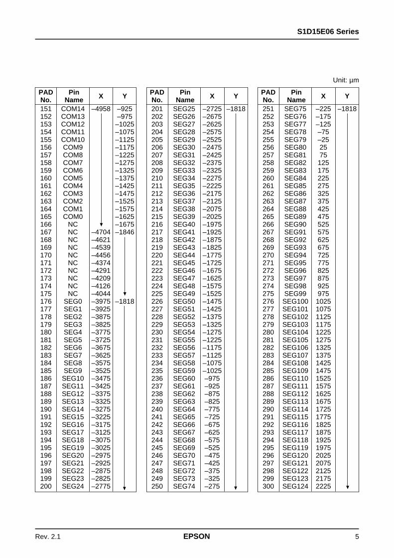
101 COM64 –4958 1575102 COM63 1525103 COM62 1475104 COM61 1425105 COM60 1375106 COM59 1325107 COM58 1275108 COM57 1225109 COM56 1175110 COM55 1125111 COM54 1075112 COM53 1025113 COM52 975114 COM51 925115 COM50 875116 COM49 825117 COM48 775118 COM47 725119 COM46 675120 COM45 625121 COM44 575122 COM43 525123 COM42 475124 COM41 425125 COM40 375126 COM39 325127 COM38 275128 COM37 225129 COM36 175130 COM35 125131 COM34 75132 COM33 25133 COM32 –25134 COM31 –75135 COM30 –125136 COM29 –175137 COM28 –225138 COM27 –275139 COM26 –325140 COM25 –375141 COM24 –425142 COM23 –475143 COM22 –525144 COM21 –575145 COM20 –625146 COM19 –675147 COM18 –725148 COM17 –775149 COM16 –825150 COM15 –875
51 D4 –170 183052 D5 –26253 D6, SCL –35454 D7, SI –44655 VSS –53856 VSS –63057 VSS –72258 VDD –81459 VDD –90660 VDD –99861 VOUT –109062 VOUT –118263 CAP1+ –127464 CAP1+ –136665 CAP1– –145866 CAP1– –155067 CAP2– –164268 CAP2– –173469 CAP2+ –182670 CAP2+ –191871 CAP3+ –201072 CAP3+ –210273 CAP3– –219474 CAP3– –228675 CAP4– –237876 CAP4– –247077 CAP4+ –256278 CAP4+ –265479 V3 –274680 V3 –283881 V2 –293082 V2 –302283 V1 –311484 V1 –320685 VC –329886 VC –339087 MV1 –348288 MV1 –357489 MV2 –366690 MV2 –375891 MV3 –385092 MV3 –394293 CPP+ –403494 CPP– –412695 CPM+ –421896 CPM– –431097 NC –440298 NC –449499 NC –4958 1675
100 COM65 1625
1 NC 4494 18302 NC 44023 TEST0 43104 TEST1 42185 TEST2 41266 TEST3 40347 TEST4 39428 TEST5 38509 VSS 3742
10 TEST6 363411 TEST7 354212 TEST8 345013 TEST9 335814 TEST10 326615 TEST11 317416 TEST12 308217 TEST13 299018 TEST14 289819 TEST15 280620 TEST16 271421 TEST17 262222 TEST18 253023 VSS 242224 FR 231425 CL 222226 DOF 213027 F1 203828 F2 194629 CA 185430 VSS 176231 TEST 167032 CS1 157833 RES 148634 A0 139435 WR, R/W 130236 RD, E 121037 CS2 111838 VDD 102639 M/S 93440 VSS 84241 CLS 75042 VDD 65843 C86 56644 VSS 47445 P/S 38246 VDD 29047 D0 19848 D1 10649 D2 1450 D3 –78
PAD Pin X YNo. NamePAD Pin X YNo. Name
PAD Pin X YNo. Name
Unit: µm
4.3 Pad Center Coordinates
S1D15E06 Series
Rev. 2.1 EPSON 5
201 SEG25 –2725 –1818202 SEG26 –2675203 SEG27 –2625204 SEG28 –2575205 SEG29 –2525206 SEG30 –2475207 SEG31 –2425208 SEG32 –2375209 SEG33 –2325210 SEG34 –2275211 SEG35 –2225212 SEG36 –2175213 SEG37 –2125214 SEG38 –2075215 SEG39 –2025216 SEG40 –1975217 SEG41 –1925218 SEG42 –1875219 SEG43 –1825220 SEG44 –1775221 SEG45 –1725222 SEG46 –1675223 SEG47 –1625224 SEG48 –1575225 SEG49 –1525226 SEG50 –1475227 SEG51 –1425228 SEG52 –1375229 SEG53 –1325230 SEG54 –1275231 SEG55 –1225232 SEG56 –1175233 SEG57 –1125234 SEG58 –1075235 SEG59 –1025236 SEG60 –975237 SEG61 –925238 SEG62 –875239 SEG63 –825240 SEG64 –775241 SEG65 –725242 SEG66 –675243 SEG67 –625244 SEG68 –575245 SEG69 –525246 SEG70 –475247 SEG71 –425248 SEG72 –375249 SEG73 –325250 SEG74 –275
251 SEG75 –225 –1818252 SEG76 –175253 SEG77 –125254 SEG78 –75255 SEG79 –25256 SEG80 25257 SEG81 75258 SEG82 125259 SEG83 175260 SEG84 225261 SEG85 275262 SEG86 325263 SEG87 375264 SEG88 425265 SEG89 475266 SEG90 525267 SEG91 575268 SEG92 625269 SEG93 675270 SEG94 725271 SEG95 775272 SEG96 825273 SEG97 875274 SEG98 925275 SEG99 975276 SEG100 1025277 SEG101 1075278 SEG102 1125279 SEG103 1175280 SEG104 1225281 SEG105 1275282 SEG106 1325283 SEG107 1375284 SEG108 1425285 SEG109 1475286 SEG110 1525287 SEG111 1575288 SEG112 1625289 SEG113 1675290 SEG114 1725291 SEG115 1775292 SEG116 1825293 SEG117 1875294 SEG118 1925295 SEG119 1975296 SEG120 2025297 SEG121 2075298 SEG122 2125299 SEG123 2175300 SEG124 2225
151 COM14 –4958 –925152 COM13 –975153 COM12 –1025154 COM11 –1075155 COM10 –1125156 COM9 –1175157 COM8 –1225158 COM7 –1275159 COM6 –1325160 COM5 –1375161 COM4 –1425162 COM3 –1475163 COM2 –1525164 COM1 –1575165 COM0 –1625166 NC –1675167 NC –4704 –1846168 NC –4621169 NC –4539170 NC –4456171 NC –4374172 NC –4291173 NC –4209174 NC –4126175 NC –4044176 SEG0 –3975 –1818177 SEG1 –3925178 SEG2 –3875179 SEG3 –3825180 SEG4 –3775181 SEG5 –3725182 SEG6 –3675183 SEG7 –3625184 SEG8 –3575185 SEG9 –3525186 SEG10 –3475187 SEG11 –3425188 SEG12 –3375189 SEG13 –3325190 SEG14 –3275191 SEG15 –3225192 SEG16 –3175193 SEG17 –3125194 SEG18 –3075195 SEG19 –3025196 SEG20 –2975197 SEG21 –2925198 SEG22 –2875199 SEG23 –2825200 SEG24 –2775
PAD Pin X YNo. NamePAD Pin X YNo. Name
PAD Pin X YNo. Name
Unit: µm

S1D15E06 Series
6 EPSON Rev. 2.1
301 SEG125 2275 –1818302 SEG126 2325303 SEG127 2375304 SEG128 2425305 SEG129 2475306 SEG130 2525307 SEG131 2575308 SEG132 2625309 SEG133 2675310 SEG134 2725311 SEG135 2775312 SEG136 2825313 SEG137 2875314 SEG138 2925315 SEG139 2975316 SEG140 3025317 SEG141 3075318 SEG142 3125319 SEG143 3175320 SEG144 3225321 SEG145 3275322 SEG146 3325323 SEG147 3375324 SEG148 3425325 SEG149 3475326 SEG150 3525327 SEG151 3575328 SEG152 3625329 SEG153 3675330 SEG154 3725331 SEG155 3775332 SEG156 3825333 SEG157 3875334 SEG158 3925335 SEG159 3975336 NC 4044 –1846337 NC 4126338 NC 4209339 NC 4291340 NC 4374341 NC 4456342 NC 4539343 NC 4621344 NC 4704345 NC 4958 –1675346 COM66 –1625347 COM67 –1575348 COM68 –1525349 COM69 –1475350 COM70 –1425
351 COM71 4958 –1375352 COM72 –1325353 COM73 –1275354 COM74 –1225355 COM75 –1175356 COM76 –1125357 COM77 –1075358 COM78 –1025359 COM79 –975360 COM80 –925361 COM81 –875362 COM82 –825363 COM83 –775364 COM84 –725365 COM85 –675366 COM86 –625367 COM87 –575368 COM88 –525369 COM89 –475370 COM90 –425371 COM91 –375372 COM92 –325373 COM93 –275374 COM94 –225375 COM95 –175376 COM96 –125377 COM97 –75378 COM98 –25379 COM99 25380 COM100 75381 COM101 125382 COM102 175383 COM103 225384 COM104 275385 COM105 325386 COM106 375387 COM107 425388 COM108 475389 COM109 525390 COM110 575391 COM111 625392 COM112 675393 COM113 725394 COM114 775395 COM115 825396 COM116 875397 COM117 925398 COM118 975399 COM119 1025400 COM120 1075
401 COM121 4958 1125402 COM122 1175403 COM123 1225404 COM124 1275405 COM125 1325406 COM126 1375407 COM127 1425408 COM128 1475409 COM129 1525410 COM130 1575411 COM131 1625412 NC 1675
PAD Pin X YNo. NamePAD Pin X YNo. Name
PAD Pin X YNo. Name
Unit: µm

S1D15E06 Series
Rev. 2.1 EPSON 7
5. PIN DESCRIPTION5.1 Power Pin
V2 11/14 • V3V1 9/14 • V3VC 7/14 • V3
MV1 5/14 • V3MV2 3/14 • V3
Pin name I/O DescriptionNumber of
pinsVDD Power Connect to system MPU power supply pin VCC. 6
supplyVSS Power Connect to the system GND. 8
supply MV3 is short circuited with MV3 inside the IC chip.V3, V2, V1, Power A liquid crystal drive multi-level power supply. The voltages 14VC, MV1, supply determined by the liquid crystal cell are impedance-converted by (2 each)MV2, MV3, resistive divider and operational amplifier for application.(=VSS) The following order must be maintained:
V3 ≥ V2 ≥ V1 ≥ VC ≥ MV1 ≥ MV2 ≥ MV3 (=VSS)Master operation: When power supply is turned on, the followingvoltage is applied to each pin by the built-in power supply circuit.MV3 is connected to with VSS inside the IC chip.
5.2 LCD Power Supply Circuit Pin
Pin name I/O DescriptionNumber of
pinsCAP1+ O Pin connected to the positive side of the step-up capacitor. 2
Connect the capacitor between this pin and CAP1– pin.CAP1– O Pin connected to the negative side of the step-up capacitor. 2
Connect the capacitor between this pin and CAP1+ pin.CAP2+ O Pin connected to the positive side of the step-up capacitor. 2
Connect the capacitor between this pin and CAP2– pin.CAP2– O Pin connected to the negative side of the step-up capacitor. 2
Connect the capacitor between this pin and CAP2+ pin.VOUT O Output pin for step-up. 2
Connect the capacitor between this pin and VDD.CAP3+ O Pin connected to the positive side of the step-up capacitor. 2
Connect the capacitor between this pin and CAP3– pin.CAP3– O Pin connected to the negative side of the step-up capacitor. 2
Connect the capacitor between this pin and CAP3+ pin.CAP4+ O Pin connected to the positive side of the step-up capacitor. 2
Connect the capacitor between this pin and CAP4– pin.CAP4– O Pin connected to the negative side of the step-up capacitor. 2
Connect the capacitor between this pin and CAP4+ pin.CPP+ O Keep it open. 1CPP– O Keep it open. 1CPM+ O Keep it open. 1CPM– O Keep it open. 1
S1D15E06 Series
8 EPSON Rev. 2.1
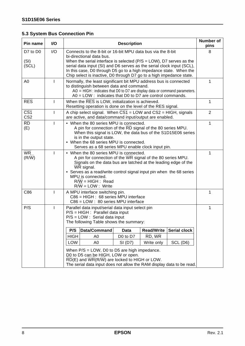
P/S Data/Command Data Read/Write Serial clockHIGH A0 D0 to D7 RD, WRLOW A0 SI (D7) Write only SCL (D6)
5.3 System Bus Connection Pin
Pin name I/O DescriptionNumber of
pinsD7 to D0 I/O Connects to the 8-bit or 16-bit MPU data bus via the 8-bit 8
bi-directional data bus.(SI) When the serial interface is selected (P/S = LOW), D7 serves as the(SCL) serial data input (SI) and D6 serves as the serial clock input (SCL),
In this case, D0 through D5 go to a high impedance state. When theChip select is inactive, D0 through D7 go to a high impedance state.
A0 I Normally, the least significant bit MPU address bus is connected 1to distinguish between data and command. A0 = HIGH : indicates that D0 to D7 are display data or command parameters. A0 = LOW : indicates that D0 to D7 are control commands.
RES I When the RES is LOW, initialization is achieved. 1Resetting operation is done on the level of the RES signal.
CS1 I A chip select signal. When CS1 = LOW and CS2 = HIGH, signals 2CS2 are active, and data/command input/output are enabled.RD I • When the 80 series MPU is connected. 1(E) A pin for connection of the RD signal of the 80 series MPU.
When this signal is LOW, the data bus of the S1D15E06 seriesis in the output state.
• When the 68 series MPU is connected.Serves as a 68 series MPU enable clock input pin.
WR I • When the 80 series MPU is connected. 1(R/W) A pin for connection of the WR signal of the 80 series MPU.
Signals on the data bus are latched at the leading edge of theWR signal.
• Serves as a read/write control signal input pin when the 68 seriesMPU is connected.
R/W = HIGH : ReadR/W = LOW : Write
C86 I A MPU interface switching pin. 1C86 = HIGH : 68 series MPU interfaceC86 = LOW : 80 series MPU interface
P/S I Parallel data input/serial data input select pin 1P/S = HIGH : Parallel data inputP/S = LOW : Serial data inputThe following Table shows the summary:
When P/S = LOW, D0 to D5 are high impedance.D0 to D5 can be HIGH, LOW or open.RD(E) and WR(R/W) are locked to HIGH or LOW.The serial data input does not allow the RAM display data to be read.

S1D15E06 Series
Rev. 2.1 EPSON 9
Pin name I/O DescriptionNumber of
pinsCLS I A pin used to select Enable/Disable state of the built-in oscillator 1
circuit for display clock. CLS = HIGH : Built-in oscillator circuit Enabled CLS = LOW : Built-in oscillator circuit Disabled (External input)When CLS is LOW, display clock is input from the CL pin. Whenthe S1D15E06 series is used in the master/slave mode, each CLSpins must be set to the same level.
M/S I A pin used to select the master/slave operation for S1D15E06 series. 1Liquid crystal display system is synchronized when the masteroperation outputs the timing signal required for liquid crystaldisplay, while the slave operation inputs the timing signal requiredfor liquid crystal display.
M/S = HIGH : Master operationM/S = LOW : Slave operation
The following Table shows the relation in conformance to the M/S and CLS:
The slave power supply circuit can also operate, but do not use it.CL I/O Display clock input/output pin. 1
The following Table shows the relation in conformance to the M/S and CLS state:
When you want to use the S1D15E06 series in the master/slavemode, connect each CL pin.
FR I/O A liquid crystal alternating current input/output pin. 1M/S = HIGH : OutputM/S = LOW : Input
When you want to use the S1D15E06 series in the master/slavemode, connect each FR pin.
F1, F2, I/O A liquid crystal sync signal input/output pin. 3CA M/S = HIGH : Output (1 each)
M/S = LOW : InputWhen you want to use the S1D15E06 series in the master/slavemode, connect each F1, F2 and CA pins.
DOF I/O A liquid crystal blanking control pin. 1M/S = HIGH : OutputM/S = LOW : Input
When you want to use the S1D15E06 series in the master/slavemode, connect each DOF pin.
M/S CLS CL
HIGH HIGH OutputLOW Input
LOW HIGH InputLOW Input
M/S CLS Oscillation Power CL FR, DOF,circuit circuit F1, F2, CA
HIGH HIGH Enabled Enabled Output OutputLOW Disabled Enabled Input Output
LOW HIGH Disabled Disabled Input InputLOW Disabled Disabled Input Input
Display clock Master SlaveBuilt-in oscillator circuit used HIGH HIGH
External input LOW LOW
S1D15E06 Series
10 EPSON Rev. 2.1
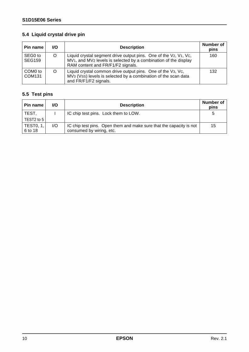
5.4 Liquid crystal drive pin
5.5 Test pins
Pin name I/O DescriptionNumber of
pinsSEG0 to O Liquid crystal segment drive output pins. One of the V2, V1, VC, 160SEG159 MV1, and MV2 levels is selected by a combination of the display
RAM content and FR/F1/F2 signals.COM0 to O Liquid crystal common drive output pins. One of the V3, VC, 132COM131 MV3 (VSS) levels is selected by a combination of the scan data
and FR/F1/F2 signals.
Pin name I/O DescriptionNumber of
pinsTEST, I IC chip test pins. Lock them to LOW. 5TEST2 to 5TEST0, 1, I/O IC chip test pins. Open them and make sure that the capacity is not 156 to 18 consumed by wiring, etc.

S1D15E06 Series
Rev. 2.1 EPSON 11
6. FUNCTIONAL DESCRIPTION6.1 MPU Interface6.1.1 Selection of Interface Type
S1D15E06 series allows data to be sent via the 8-bit bi-directional data buses (D7 to D0) or serial data input (SI). Bysetting the polarity of the P/S pin to HIGH or LOW, you can select either 8-bit parallel data input or serial data input,as shown in Table 6.1.
Table 6.1
6.1.2 parallel interface
When the parallel interface is selected (P/S = HIGH), direction connection to the MPU bus of either 80 series MPU or68 series MPU is performed by setting the 86 pin to either HIGH or LOW, as shown in Table 6.2.
Table 6.2
The data bus signals are identified by a combination of A0, RD (E), and WR (R/W) signals as shown in Table 6.3.
Table 6.3
6.1.3 Serial interface
When the serial interface is selected (P/S =LOW), the chip is active (CS1 = LOW, CS2 = HIGH), and reception of serialdata input (SI) and serial clock input (SCL) is enabled. Serial interface comprises a 8-bit shift register and 3-bit counter.The serial data are latched by the rising edge of serial clock signals in the order of D7, D6, .... and D0 starting from theserial data input pin. On the rising edge of 8th serial clock signal, they are converted into 8-bit parallel data to beprocessed.Whether serial data input is a display data or command is identified by A0 input. A0 = HIGH indicates display data,while A0 = LOW shows command data. The A0 input is read and identified at every 8 × n-th rising edge of the serialclock after the chip has turned active.Fig. 6.1 shows the serial interface signal chart.
P/S CS1 CS2 A0 RD WR D7 to D0
HIGH : 68 series MPU bus CS1 CS2 A0 E R/W D7 to D0LOW : 80 series MPU bus CS1 CS2 A0 RD WR D7 to D0
Common 68 series 80 series
A0 R/W RD WRFunction
1 1 0 1 Display data read, status read
1 0 1 0 Display data write, command parameter write
0 1 1 0 Command write
P/S CS1 CS2 A0 RD WR C86 D7 D6 D5 to D0
HIGH : Parallel input CS1 CS2 A0 RD WR C86 D7 D6 D5 to D0LOW : Serial input CS1 CS2 A0 — — — SI SCL (HZ)
—: Fixed to HIGH or LOW HZ: High impedance state

S1D15E06 Series
12 EPSON Rev. 2.1
6.1.4 Chip Selection
The S1D15E06 series has two chip select pins; CS1 andCS2. MPU interface or serial interface is enabled onlywhen CS1 = LOW and CS2 = HIGH.When the chip select pin is inactive, D0 to D5 are in thestate of high impedance, while A0, RD and WR inputsare disabled. When serial interface is selected, the shiftregister and counter are reset.
6.1.5 Access to display data RAM andinternal register
Access to S1D15E06 series viewed from the MPU sideis enabled only if the cycle time requirements are kept.This does not required waiting time; hence, high-speeddata transfer is allowed.Furthermore, at the time of data transfer with the MPU,S1D15E06 series provides a kind of inter-LSI pipe line
processing via the bus holder accompanying the internaldata bus.For example, when data is written to the display dataRAM by the MPU, the data is once held by the busholder. It is written to the display data RAM before thenext data write cycle comes.On the other hand, when the MPU reads the content ofthe display data RAM, it is read in the first data readcycle (dummy), and the data is held in the bus holder.Then it is read onto on the system bus from the busholder in the next data read cycle. Restrictions areimposed on the display data RAM read sequence. Whenthe address has been set, specified address data is notoutput to the Read command immediately after that.The specified address data is output in the second datareading. This must be carefully noted. Therefore, onedummy read operation is mandatory subsequent toaddress setting or write cycle. Fig. 6.2 illustrates thisrelationship.
Fig. 6.1
* When the chip is inactive, the counter is reset to the initials state.* Reading is not performed in the case of serial interface.* For the SCL signal, a sufficient care must be taken against terminal reflection of the wiring and external noise.
Recommend to use an actual equipment to verify the operation.
CS2SI
SCL
A0
CS1
D7
1 2 3 4 5 6 7 8 9 10 11 12 13 14
D6 D5 D4 D3 D2 D7 D6 D5 D4 D3 D2D1 D0

S1D15E06 Series
Rev. 2.1 EPSON 13
Write
White
Latch
N N+1 N+2
N N+1 N+2
WR
MP
UIn
tern
al ti
min
g
DATA
Command
BUS Holder
Write Signal
A0
Read
Fig. 6.2
Read Dumy n n+1
N+2Increment N+1Preset N
Read command code n n+1 n+2
Data ReadData ReadDummy Read
WR
RD
DATA
Read Signal
Column Address
Bus Holder
MP
UIn
tern
al ti
min
g
A0
Command
6.2 Display data RAM6.2.1 Display Data RAM
This is a RAM to store the display dot data, and comprises132 × 160 × 2 bits. Access to the desired bit is enabledby specifying the page address and column address.When the 4 gray-scale is selected by the Display Modecommand, display data input for gray-scale display areprocessed as a two-bit pair. Combination is as follows:
(MSB, LSB) = (D1,D0), (D3,D2), (DS,D4), (D7,D6)
When the RAM bit data is gray-scale 1 and 2, gray-scaledisplay is realized according to the parameter of theGray-scale Pattern Set command.
RAM bit data (high order and low order)(1,1) : gray-scale 3 Black (when display is in
normal mode)(1,0) : gray-scale 2(0,1) : gray-scale 1(0,0) : gray-scale 0 White (when display is in
normal mode)
When binary display is selected by the Display Modecommand, the RAM 1 bit built in the one-dot pixelresponds to it. When the RAM bit data is “1”, thedisplay is black. If it is “0”, the display is given in white. RAM bit data
“1” : Light On Black (when display is innormal mode)
“0” : Light Off White (when display is innormal mode)

S1D15E06 Series
14 EPSON Rev. 2.1
Fig. 6.3 4 gray-scale
(D1,D0)
(D3,D2)
(D5,D4)
(D7,D6)
(0,0)
(1,1)
(0,0)
(0,0)
(1,1)
(0,0)
(1,0)
(0,0)
(1,1)
(0,0)
(0,1)
(0,0)
(0,0)
(0,0)
(0,0)
(0,0)
Display data RAM
COM0
COM1
COM2
COM3
LCD
Display data D7 to D0 from the MPU correspond toLCD common direction, as shown in Fig. 6.3 and 6.4.Therefore, less restrictions when multi-chip usage.Furthermore, read/write operations from the MPU tothe RAM are carried out via the input/output buffer.
The read operation from Display data RAM is designedas an independent operation. Accordingly, even if theMPU accesses the RAM asynchronously during LCDdisplay, no adverse effect is given to display.
Fig. 6.4 Binary
6.2.2 Gray-scale display
When the 4 gray-scale is selected by the Display Modecommand, gray-scale is represented by the FRM controlcarried out according to the gray-scale data written inthe display data RAM.Of the 4 gray-scale, 2 gray-scale of halftones (gray-scale 2 and 1) has its level of contrast specified by theGray-scale Set command. Gray-scale can be selectedfrom 6 levels of contrast.
6.2.3 Page address circuit/column addresscircuit
The address of the display data RAM to be accessed isspecified by the Page Address Set command and ColumnAddress Set command, as shown in Fig. 6.5 and Fig. 6.6.For Address incremental direction, either the columndirection or page direction can be selected by the AddressDirection command. Whichever direction is chosen,increment is carried out by positive one (+1) after write
or read operation.When the column direction is selected for addressincrement, the column address is increased by +1 forevery write or read operation. After the column addresshas accessed up to 9FH, the page address is incrementedby +1 and the column address shifts to 0H.When the page direction is selected for addressincrement, the page address is increased with the columnaddress locked in position. When the page address hasaccessed up to 32H, the column address is incrementedby +1, and the page address goes to 0H.Whichever direction is selected for address increment,the page address goes back to 0H and the columnaddress to 0H after access up to the column address 9FHof page address 32H.As shown in Fig. 6.4, relationship between the displaydata RAM column address and segment output can bereversed by the Column Address Set Direction command.This will reduce restrictions on IC layout during LCDmodule assembling.
D0
D1
D2
D3
D4
0
1
0
0
1
1
0
0
1
0
1
0
0
1
0
1
0
0
1
0
0
0
0
0
0
Display data RAM
COM0
COM1
COM2
COM3
COM4
LCD

S1D15E06 Series
Rev. 2.1 EPSON 15
6.2.4 Line address circuit
The line address circuit specifies the line addresscorresponding to COM output when the contents of thedisplay data RAM is displayed, as shown in Fig. 6.5 and6.6. Normally, the top line of the display (COM0 outputin the case of normal rotation of the common outputstatus and COM131 output in the case of reverse rotation)is specified by the Display Start Line Address Setcommand. The display area starts from the specifieddisplay start line address to cover the area correspondingto the lines specified by the DUTY Set command in thedirection where the line address increments.If the display start line address set command is used for
Table 6.4
SEG output SEG0 SEG159ADC “0” 0(H)→ Column Address →9F(H)(D0) “1” 9F(H)← Column Address ←0(H)
dynamic modification of the line address, screen scrolland page change are enabled.
6.2.5 Area scroll
The display area can be divided into the display areafixed in the COM direction and scrollable area by thearea scroll command. The scroll area is set by a scrollmode, scroll start line address (AS), scroll end address(AE), and scroll display line count (AL) as parametersfor the area scroll command. Display start line address(DL) in the scroll area can be specified by the displaystart line address set command.
6.2.5.1 Mode 0 (full screen scroll)
This mode releases the area scroll. Parameters AS, AEand AL are disabled,
6.2.5.2 Mode 1 (Upper scroll )
Reading starts from the line address DL to read AL linesas a scroll area. If the line address AE is read in the
middle of reading the scroll area, the line address to beread next will be 00H. When all the AL lines have beenread, the address to be read next will be AE + 1. Whenreading is completed up to the final line address, thecontrol goes back to the line address DL, and parameterAS is disabled. DL can be specified in the range from00H to AE.
ScrollableScrollable
Fixed area
Fixed area
Scrollable
Fixed area
Fixed area
Scrollable
Mode 0 Mode 1 Mode 2 Mode 3
Upper fixed areaNumber of line : AS
Scroll areaNumber of line : AL
Lower fixed areaNumber of line
00H
DL
AE+1
Final line address
AS-1
Scroll mode

S1D15E06 Series
16 EPSON Rev. 2.1
6.2.5.3 Mode 2 (lower scroll)
Reading starts from line address 00H to reach the lineaddress AS-1 in the continuous reading mode. Uponcompletion of reading of line address AS-1, the lineaddress moves to the DL to read the area correspondingto AL lines from the line address DL as a scroll area. Ifthe final line address is read in the middle of reading thescroll area, the line address to be read next will be AS.When all AL lines have been read, the control goes backto the line address 00H, and parameter AE is disabled.DL can be specified in the range from AS to the final lineaddress.
6.2.5.4 Mode 3 (Center scroll)
Reading starts from line address 00H to reach the lineaddress AS-1 in the continuous reading mode.Upon completion of reading of line address AS-1, theline address moves to the DL to read the areacorresponding to AL lines from the line address DL asa scroll area. If the final line address is read in themiddle of reading the scroll area, the line address to beread next will be AS. When all AL lines have been read,the line address will be AE+1. When up to the final lineaddress has been read, the control goes back to the lineaddress 00H, DL can be specified in the range from ASto AE.
6.2.6 Display data latch circuit
The display data latch circuit is a latch to temporarilylatch the display data output from then display dataRAM to the liquid crystal drive circuit. Display normal/reverse, display ON/OFF, and display all lighting ON/OFF commands control the data in this latch, withoutthe data in the display data RAM being controlled.
6.2.7 Partial display
Partial display of the screen is provided by the partialdisplay ON/OFF command. The partial area (displaystart line, number of display lines) are set by the partialdisplay set command.The display start line of the parameter shows the lineassigned in the COM direction of the liquid crystalscreen. It is different from the line address given in Fig.6.5 and 6.6.
Example: When the point is set at 1 (COM4 to 7) by theDuty Reset command, the display line isassigned as shown below. If the display startline 4 and display line count 3 are specifiedby the partial display set command, the displayarea is COM8 to COM10.
Display line LCD panel0123456789
10
COM4COM5COM6COM7COM8COM9COM10COM11COM12COM13COM14

S1D15E06 Series
Rev. 2.1 EPSON 17
Fig. 6.5 4 gray-scale
Page AddressData
D1,D0
D3,D2
D5,D4
D7,D6
D1,D0D3,D2
D5,D4
D7,D6
D1,D0D3,D2
D5,D4
D7,D6
D1,D0D3,D2
D5,D4
D7,D6
D1,D0D3,D2
D5,D4
D7,D6
D1,D0D3,D2
D5,D4
D7,D6
D1,D0D3,D2
D5,D4
D7,D6
D1,D0D3,D2
D5,D4
D7,D6
D5 D4 D3 D2 D1 D0
0
0
0
0
0
0
0
1
0
0
0
0
0
0
1
0
0
0
0
0
0
0
1
0
0
0
0
0
1
1
1
0
0
0
1
1
0
0
1
0
0
1
0
1
0
1
1
0
Start
Line
Address
COM
Output
CommonOutput state:
Normal rotation
COM0
COM1
COM2
COM3
COM4
COM4
COM6
COM7
COM8
COM9
COM10
COM11
COM12
COM13
COM14
COM15
COM16COM17
COM18
COM19
COM20
COM21
COM22COM23
COM124COM125
COM126
COM127
COM128
COM129
COM130
COM131
Page 0
Page 1
Page 2
Page 3
Page 4
Page 5
Page 31
Page 32
SE
G0
SE
G1
SE
G2
SE
G3
SE
G4
SE
G5
SEG
154
SEG
155
SEG
156
SEG
157
SEG
158
SEG
159
LCD
Out
9F 9E 9D 9C 9B 9A 05 04 03 02 01 00 1 D0
00 01 02 03 04 05 9A 9B 9C 9D 9E 9F 0 D0
AD
C
Col
umn
Add
ress
132
lines
00H
01H
02H
03H
04H
05H
06H
07H
08H09H
0AH
0BH
0CH0DH
0EH
0FH
10H
11H12H
13H
14H
15H
16H
17H
7CH7DH
7EH
7FH
80H
81H
82H
83H
4 gray-scale display
When the display start line is set to 11H

S1D15E06 Series
18 EPSON Rev. 2.1
Fig. 6.6 Binary display
D0D1D2D3D4D5D6D7D0D1D2D3D4D5D6D7D0D1D2D3D4D5D6D7D0D1D2D3D4D5D6D7D0D1D2D3D4D5D6D7D0D1D2D3D4D5D6D7D0D1D2D3D4D5D6D7D0D1D2D3D4D5D6D7D0D1D2D3D4D5D6D7D0D1D2D3D4D5D6D7D0D1D2D3D4D5D6D7D0D1D2D3D4D5D6D7
COM0COM1COM2COM3COM4COM5COM6COM7COM8COM9
COM10COM11COM12COM13COM14COM15COM16COM17COM18COM19COM20COM21COM22COM23COM24COM25COM26COM27COM28COM29COM30COM31COM32COM33COM34COM35COM36COM37COM38COM39COM40COM41COM42COM43COM44COM45COM46
COM121COM122COM123COM124COM125COM126COM127COM128COM129COM130COM131
0 0 0 0 Page 0
0 0 0 1 Page 1
0 0 1 0 Page 2
0 0 1 1 Page 3
0 1 0 0 Page 4
0 1 0 1 Page 5
1 1 1 1 Page 15
0 0 0 0 Page 16
Page 17
Page 18
Page 31
Page 32
Page AddressD3 D2 D1 D0 Data
LineAddress
COMOutput
Commonoutput state: Normal mode
Binary display
When the display start line is set to 0CH
Start
0 0 0 1
0 0 1 0
1 1 1 1
0 0 0 0
SE
G0
SE
G1
SE
G2
SE
G3
SE
G4
SE
G5
SE
G6
SE
G7
9F 9E 9D 9C 9B 9A 99 98
00 01 02 03 04 05 06 07
SE
G15
2S
EG
153
SE
G15
4S
EG
155
SE
G15
6S
EG
157
SE
G15
8S
EG
159
07 06 05 04 03 02 01 00
98 99 9A 9B 9C 9D 9E 9F
LCD
Out
AD
C
Col
umn
Add
ress
1 D0
0 D0
00H01H02H03H04H05H06H07H08H09H0AH0BH0CH0DH0EH0FH10H11H12H13H14H15H16H17H18H19H1AH1BH1CH1DH1EH1FH20H21H22H23H24H25H26H27H28H29H2AH2BH2CH2DH2EH2FH30H79H7AH7BH7CH7DH7EH7FH80H81H82H83H84H85H86H87H88H89H8AH8BH8CH8DH8EH8FH90H91H92H93H94H95H96H4FH50HF9HFAHFBHFCHFDHFEHFFH100H101H102H103H104H105H106H107H
D5 D4
0 0
0 0
0 0
0 0
0 0
0 0
0 0
0 1
0 1
0 1
0 1
1 0
........
.
........
.....
.....
........
.
........
.....
.....
........
.
132
lines

S1D15E06 Series
Rev. 2.1 EPSON 19
Operating mode CL FR, CA, F1, F2, DOFMaster (M/S = HIGH) Built-in oscillator circuit enabled (CLS = HIGH) Output Output
Built-in oscillator circuit disabled (CLS = LOW) Input OutputSlave (M/S = LOW) Built-in oscillator circuit enabled (CLS = HIGH) Input Input
Built-in oscillator circuit disabled (CLS = LOW) Input Input
Table 6.5
6.3 Oscillator circuitA display clock is generated by the CR oscillator. Theoscillator circuit is enabled only when M/S = HIGH andCLS = HIGH. Oscillation starts after input of the built-in oscillator circuit ON command input.When CLS = LOW, oscillation stops, and display clockis input from the CL pin.
6.4 Display timing generation circuitTiming signals are generated from the display clock tothe line address circuit and display data latch circuit.Synchronized with display clock, display data is latchedin display data latch circuit, and is output to the segmentdrive output pin. Reading of the display data into theLCD drive circuit is completely independent of accessfrom the MPU to the display data RAM. Accordingly,asynchronous access to the display data RAM duringLCD display does not give any adverse effect; like as
flicker.Furthermore, the display clock generates internalcommon timing, liquid crystal alternating signal(FR),field start signal (CA) and drive pattern signal (Fl andF2).The FR normally generates 2-frame alternating drivesystem drive waveform to the liquid crystal drivecircuit. The n-line reverse alternating drive waveformis generated for each 4 × (a+1) line by setting data on then-line reverse drive register. When there is a displayquality problem including crosstalk,the problem maybe solved using the n-line reverse alternating drive.Execute liquid crystal display to determine the numberof lines “n” for alternation.When you want to use the S1D15E06 series in multi-chip configuration, supply display timing signal (FR,CA, F1, F2, CL, DOF) to the slave side from the masterside. Table 6.5 shows the statuses of FR, CA, F1, F2,CL, DOF.
6.5 Liquid crystal drive circuit6.5.1 SEG Drivers
This is a SEG output circuit. It selects the five values ofV2, V1, VC, MV1 and MV2 using the driver controlsignal determined by the decoder, and output them.
6.5.2 COM Drivers
This is a COM output circuit. It selects three values ofV3, VC and MV3(VSS) using the driver control signaldetermined by the decoder, and output them.S1D15E06 series allows the COM output scanningdirection to be set by the common output status selectcommand. (See Table 6.6). This will reduce restrictionson IC layout during LCD module assembling.
Status Direction of COM scanningNormal COM 0 → COM 131Reverse COM 131 → COM 0
Table 6.6

S1D15E06 Series
20 EPSON Rev. 2.1
Circuits used D4 D3 D2 D1 D0 Step-up VC regulator LCDV Eternal inputcircuit circuit circuit power supply
1 Use of all built-inpower supplies
Triple step-up 1 1 1 1 1 “1” “1” “1” – Double step-up 1 0 1 1 1 “1” “1” “1” –
VOUT = VDD 0 1 1 1 1 “1” “1” “1” – 2 VC regulating circuit and 0 0 0 1 1 ××××× “0” “1” “1” VOUT
LCDV circuit only 3 LCDV circuit only 0 0 0 0 1 ××××× “0” ××××× “0” “1” VC
4 External power supply 0 0 0 0 0 ××××× “0” ××××× “0” ××××× “0” V3, V2, V1, VC,only (S1D15E06D00B*) MV1, MV2
* Any combinations other than the above are not available.
*100ms or more should be kept from VC regulator circuit ON to LCDV circuit ON.
Table 6.8 Reference combination
Table 6.7 Control by 5-bit data of the control set command
Item State Triple Double Single“1” “0”
D4 Step-cut circuit scaling factor select bit 1 – – 1 1 0D3 Step-cut circuit scaling factor select bit 2 – – 1 0 1D2 Step-cut circuit control bit ON OFF – – –D1 Voltage regulator circuit (VC regulator circuit) control bit ON OFF – – –D0 LCD driving potential generating circuit (LCDV circuit) control bit ON OFF – – –
6.6 Power supply circuitThis is a power supply circuit to generate voltagerequired for liquid crystal drive, and is characterized bya low power consumption. It consists of a step-upcircuit, voltage regulating circuit and liquid crystaldrive voltage generating circuit, and is enabled onlyduring master operation. The power supply circuit usesthe power control set command to provide an on/off
control of step-up circuit, voltage regulating circuit andliquid crystal drive potential generating circuit. Thisallows a combined use of the external power supply andpart of built-in power supply functions. Table 6.7shows functions controlled by the 5-bit data of thecontrol set command, and Table 6.8 shows referencecombinations. The power supply circuit is enabled onlyduring master operation.
S1D15E06 Series
Rev. 2.1 EPSON 21
S1D
15E
06
S1D
15E
06
VDD
VOUT
CAP1+
CAP1–
C1
C1
C1
C1
C1
+
+
VDD
VOUT
CAP1+
CAP1–
CAP2–
CAP2+ CAP2+
CAP2–
+
+
+
VDD = 2V
VSS = 0V
VOUT = 3 x VDD
= 6V
VDD = 3V
VSS = 0V
VOUT = 2 x VDD
= 6V
S1D
15E
06
VDD
VOUT
CAP1+
CAP1–
OPEN CAP2+
CAP2–
VSS = 0V
VOUT = VDD
= 3.6V
OPENOPEN
OPEN
OPEN
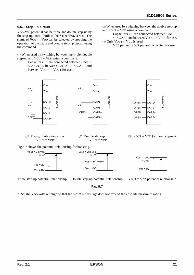
6.6.1 Step-up circuit
VDD-VSS potential can be triple and double step-up bythe step-up circuit built in the S1D15E06 series. Thestatus of VOUT = VDD can be selected by stopping theoperation of the triple and double step-up circuit usingthe command
1 When used by switching between the triple, doublestep-up and VOUT = VDD using a command:
Capacitors C1 are connected between CAP1+<-> CAP1, between CAP2+ <-> CAP2 andbetween VDD <-> VOUT for use.
2 When used by switching between the double step-upand VOUT = VDD using a command:
Capacitors C1 are connected between CAP1+<-> CAP1 and between VDD <-> VOUT for use.
3 Only VOUT = VDD is used.VDD pin and VOUT pin are connected for use.
2 Double step-up orVOUT = VDD
1 Triple, double step-up orVOUT = VDD
3 VOUT = VDD (without step-up)
Triple step-up potential relationship Double step-up potential relationship VOUT = VDD potential relationship
Fig. 6.7
* Set the VDD voltage range so that the VOUT pin voltage does not exceed the absolute maximum rating.
Fig.6.7 shows the potential relationship for boosting.

S1D15E06 Series
22 EPSON Rev. 2.1
6.6.2 Voltage Regulating Circuit
VOUT generated from the step-up circuit or VOUT inputfrom the outside produces liquid crystal drive voltageVC via the voltage regulating circuit. The voltageregulating circuit is controlled by liquid crystal drivevoltage change command and electronic volume.The S1D15E06 series has a high precision constantvoltage source, and incorporates 4-step liquid crystaldrive voltage change command and 128-step electronicvolume functions. This makes it possible to provide ahigh precision liquid crystal drive voltage regulation
only by the command without adding any external parts.The variable range of the VC voltage is from about 1.6to 7.0 [V]. When the internal step-up is used, or VOUT
is input for use, the VOUT potential should be, inprinciple, the voltage 20% or more higher than themaximum voltage of the VC to be used, givingconsideration to temperature characteristics.
Example: When VC output is 7 [V], VOUT ≥ 8.4 [V](three times 2.8 [V], etc.)When VC output is 4 [V], VOUT ≥ 4.8 [V](two times 2.4 [V], three times 1.8 [V])
• Electronic volume
α of Table 6.9 indicates an electronic volume commandvalue. It takes one of 128 states when the data is set inthe 7-bit electronic volume register.Table 6.9 shows the value of α by setting the data in theelectronic volume register.
Table 6.9
D6 D5 D4 D3 D2 D1 D0 ααααα Voltage VC
0 0 0 0 0 0 0 0 Small0 0 0 0 0 0 1 1 ↑0 0 0 0 0 1 0 2
1 1 1 1 1 0 1 1251 1 1 1 1 1 0 126 ↓1 1 1 1 1 1 1 127 Large
• Liquid crystal drive voltage selection
The liquid drive voltage range can be selected from 3states by the liquid crystal drive voltage select commandusing the two-bit crystal drive voltage select commandregister.
Table 6.10
D1 D0 VC voltage output range0 0 1.77V to 3.50V1 0 2.53V to 5.00V1 1 3.54V to 7.00V

S1D15E06 Series
Rev. 2.1 EPSON 23
7
6
5
4
3
2
1
0
VC
Value of electronic volume α
32 64 96 127
Figure 6.8
Equation A-1 represents VC logical values. For the output voltage of VC, a manufacturing dispersion of up to ± 3%should be taken into account.
Equation A-1Unit [V]
Electronic LCD voltage selectionVR D1 D0 D1 D0 D1 D0ααααα 0 0 1 0 1 1
VC (Max.) = 3.50V VC (Max.) = 5.00V VC (Max.) = 7.00V0 to 31 1.77 + 0.0195 × α 2.53 + 0.028 × α 3.54 + 0.039 × α
32 to 63 2.39 + 0.0156 × (α–32) 3.42 + 0.0223 × (α–32) 4.78 + 0.0313 × (α–32)64 to 95 2.89 + 0.0117 × (α–64) 4.12 + 0.0167 × (α–64) 5.77 + 0.0234 × (α–64)
96 to 127 3.26 + 0.0078 × (α–96) 4.65 + 0.0112 × (α–96) 6.52 + 0.0156 × (α–96)

S1D15E06 Series
24 EPSON Rev. 2.1
An example of circuit around the power supply circuit1Use of all built-in power supplies
When used by switching between the triple, doubleboosting and VOUT = VDD: (12 C’s)
When used by switching between the double boostingand VOUT = VDD: (11 C’s)
+
++++
CAP1+CAP1–CAP2–CAP2+
VOUT
VDD
C1
++
+
C1
CPP+CPP–CPM+CPM–
V3
V2
V1
VC
MV1
MV2
MV3(VSS)
VDD
VSS
VDD
VSS
C3 × 6
+ CAP3+CAP3–CAP4–CAP4+
C1
+C1
C1C1
+
++++
CAP1+CAP1–CAP2–CAP2+
VOUT
VDD
C1
++
CPP+CPP–CPM+CPM–
V3
V2
V1
VC
MV1
MV2
MV3(VSS)
C3 × 6
+ CAP3+CAP3–CAP4–CAP4+
C1
+C1
C1C1
S1D
15E
06 S
erie
s
S1D
15E
06 S
erie
s
++
++
6.6.3 Liquid crystal drive voltage generation circuit
Voltage VC is boosting in the IC to generate potential V3. Furthermore, voltages V3 and VC are converted by resistivedivider to produce V2, V1, MV1 and MV2 voltages. V2, V2, MV1 and MV2 voltages are impedance-converted by thevoltage follower, and is supplied to the liquid crystal drive circuit.
V2 11/14 • V3V1 9/14 • V3VC 7/14 • V3
MV1 5/14 • V3MV2 3/14 • V3

S1D15E06 Series
Rev. 2.1 EPSON 25
Only VOUT = VDD is used: (9 C’s) 2VC regulating circuit and LCDV circuitVOUT external input (10 C’s)
3LCDV circuit onlyVC external input (9 C’s)
4External power supply onlyexternal input (1 C)
++++
CAP1+CAP1–CAP2–CAP2+
VOUT
VDD +
CPP+CPP–CPM+CPM–
V3
V2
V1
VC
MV1
MV2
MV3(VSS)
VDD
VSS
VDD
VSS
C3 × 6
+ CAP3+CAP3–CAP4–CAP4+
C1
+C1
C1
++++
CAP1+CAP1–CAP2–CAP2+
VOUT
VDD +
CPP+CPP–CPM+CPM–
V3
V2
V1
VC
MV1
MV2
MV3(VSS)
C3 × 6
+ CAP3+CAP3–CAP4–CAP4+
C1
+C1
C1
VOUT
S1D
15E
06 S
erie
s
S1D
15E
06 S
erie
s
++
++
+++
+
CAP1+CAP1–CAP2–CAP2+
VOUT
VDD +
CPP+CPP–CPM+CPM–
V3
V2
V1
VC
MV1
MV2
MV3(VSS)
VDD
VSS
C3 × 6
+ CAP3+CAP3–CAP4–CAP4+
C1
+C1
C1
S1D
15E
06 S
erie
s
VC
CAP1+CAP1–CAP2–CAP2+
VOUT
VDD +
CPP+CPP–CPM+CPM–
V3
V2
V1
VC
MV1
MV2
MV3(VSS)
VDD
VSSCAP3+CAP3–CAP4–CAP4+
C1
ExternalPowerSupply
S1D
15E
06 S
erie
s
++

S1D15E06 Series
26 EPSON Rev. 2.1
Examples of common reference settings
Item Settings UnitC1 1.0 to 4.7 µFC2 0.47 to 1.0C3 0.47 to 1.0
The optimum values for above-mentioned Cl, C2 andC3 vary according to the LCD panel to drive. Use theabove-mentioned values as references. Actually verifythe display of a pattern with big load to make a decision.
6.6.4 Temperature gradient select circuit
This is a circuit to select the temperature gradientcharacteristics of the liquid crystal drive power supplyvoltage. Temperature gradient characteristics can beselected from eight states by the Temperature Gradientcommand. Selection of temperature gradientcharacteristics conforming to the temperaturecharacteristics of the liquid crystal to be used makes itpossible to configure a system without providing anexternal element for temperature characteristicscompensation.
6.7 Reset circuitWhen the RES input becomes LOW, this LSI is set to theinitialized state.The following shows the initially set state:
1. Display : OFF2. Display OFF mode : VSS output3. Display : normal mode4. Display all lighting : OFF5. Common output status : normal6. Display start line : Set to 1st line7. Page address : Set to 0 page8. Column address : Set to 0 address9. Display data input direction : Column direction10. Column address direction : forward11. n-line a.c. reverse drive : OFF (reverse drive for
each frame)12. n-line reverse drive register : (D4, D3, D2, D1, D0)
= (0, 1, 1, 0, 0)13. Display mode : 4 gray-scale display14. Gray-scale pattern register : (D7, D6, D5, D4, D3,
D2, D1, D0) = (*, 1, 0, 1, *, 0, 1, 0)15. Area scroll :
Scroll mode : (D1, D0) = (0, 0)Scroll start address : (D7, D6, D5, D4, D3, D2, D1,D0) = (0, 0, 0, 0, 0, 0, 0, 0)Scroll terminating address : (D7, D6, D5, D4, D3,D2, D1, D0) = (0, 0, 0, 0, 0, 0, 0, 0)Number of display lines : (D7, D6, D5, D4, D3, D2,D1, D0) = (0, 0, 0, 0, 0, 0, 0, 0)
16. DUTY register : (D5, D4, D3, D2, D1, D0) = (1, 0,0, 0, 0, 0) (1/132 duty)Start spot (block) register : (D5, D4, D3, D2, D1,D0) = (0, 0, 0, 0, 0) (COM0)
17. Partial display : OFF18. Partial display start line : (D7, D6, D5, D4, D3, D2,
D1, D0) = (0, 0, 0, 0, 0, 0, 0)Number of partial display lines : (D7, D6, D5, D4,D3, D2, D1, D0) = (0, 0, 0, 0, 0, 0, 0)
19. Read modify write : OFF20. Built-in oscillation circuit : stop21. Oscillation frequency register : (D3, D2, D1,D0) =
(0, 0, 0, 0) (120 kHz)22. Power control register : (D4, D3, D2, D1, D0) = (0,
0, 0, 0, 0)23. Clock frequency for step-up/step-down
Step-up : (D2, D1, D0) = (1, 0, 1)Step-down : (D6, D5, D4) = (1, 0, 1)
24. Liquid crystal drive voltage selection register :(D1,D0) = (0, 0)
25. Electronic volume register : (D6, D5, D4, D3, D2,D1, D0) = (0, 0, 0, 0, 0, 0, 0)
26. Discharge : ON (only for when RES = LOW)27. Power save : OFF28. Temperature gradient resistor : (D2, D1, D0) = (0,
0, 0) (–0.06/°C)29. Register data in the serial interface : Clear
When the Reset command is used, only the above-mentioned inilialized items 7, 8 and 19 are executed.
When power is turned on, initialization by the RES pinis necessary. After initialization by the RES pin, eachinput pin must be controlled correctly.Furthermore, when control signals from the MPU havea high impedance, the excessive current may flow to theIC.After VDD is applied, measures should be taken toensure that the input pin does not have a high impedance.The S1D15E06 series discharges the electric charge ofVOUT and liquid crystal drive voltage (V3, V2, V1, VC,MV1, MV2) at the level of RES pin = LOW. Whenliquid crystal drive external power supply is used,external power supply should not be supplied during theperiod of RES = LOW to prevent external power supplyand VDD from being short circuited.
*5 Precautions when installing the COGWhen installing the COG, it is necessary to duly considerthe fact that there exists a resistance of the ITO wiringoccurring between the driver chip and the externallyconnected parts (such as capacitors and resistors). Bythe influence of this resistance, non-conformity mayoccur with the indications on the liquid crystal display.When installing the COG, we recommend to use the "4External power supply only"

S1D15E06 Series
Rev. 2.1 EPSON 27
7. COMMANDThe S1D15E06 series identifies data bus signals by a combination of A0, RD(E) and WR(R/W). Interpretation andexecution of the command are executed by the internal timing alone which is independent of the external clock. Thisallows high-speed processing.The 80 series MPU interface allows the command to be started by entering the low pulse in the RD pin during readingand by entering the low pulse in the WR pin during writing.The 68 series MPU interface allows a read state to occur by entering HIGH in the R/W pin, and permits a write stateto occur by entering LOW. It also allows the command to be started by entering the high pulse in the pin E. (For timing,see the description of “10. Timing characteristics”).
Accordingly, the 68 series MPU interface is different from 80 series MPU interface in that RD(E) is “1(H)” in the caseof display data/read shown in the Command Description and Command Table. The following describes the commands,based on the example of the 80 series MPU interface:When the serial interface is selected, enter data sequentially starting from D7.
Command Description
(1) Display ON/OFF
This command sets the display ON/OFF.When display OFF is specified, segment and common drivers outputs the level selected by the display OFF Mode Selectcommand.
E R/WA0 RD WR D7 D6 D5 D4 D3 D2 D1 D0 Output level0 1 0 1 0 1 0 1 1 1 0 Display OFF
1 Display ON
E R/WA0 RD WR D7 D6 D5 D4 D3 D2 D1 D0 Output level0 1 0 1 0 1 1 1 1 1 0 VSS
1 VC
(3) Display Normal/Reverse
This command allows the display ON/OFF state to be reversed, without having to rewrite the contents of the displaydata RAM. In this case, contents of the display data RAM are maintained.
(2) Display OFF Mode Select
This command is used to set the output level of the segment and common driver when the display is off.In the initial setting state, it becomes "D0 = 0".* When D0 = 0 is selected in the case of S1D15E06D00B*, the MV2 and common driver VSS level is output by segment
driver when display is off. Select D0 = 1 to use the S1D15E06D00B*.
E R/WA0 RD WR D7 D6 D5 D4 D3 D2 D1 D0 Setting0 1 0 1 0 1 0 0 1 1 0 RAM data = HIGH
LCD ON Voltage(normal)
1 RAM data = LOWLCD ON Voltage(reverse)

S1D15E06 Series
28 EPSON Rev. 2.1
E R/WA0 RD WR D7 D6 D5 D4 D3 D2 D1 D0 Selected state0 1 0 1 1 0 0 0 1 0 0 Normal COM0 → COM131
1 Reverse COM131 → COM0
(4) Display All Lighting ON/OFF
This command forces all the displays to be turned on independently of the contents of the display data RAM. In thiscase, the contents of the display data RAM are maintained. Fully white display can also be made by a combination ofthe Display Reverse command.
E R/WA0 RD WR D7 D6 D5 D4 D3 D2 D1 D0 Setting0 1 0 1 0 1 0 0 1 0 0 Normal display status
1 Display all lighting
(5) Common Output Status Select
This command allows the scanning direction of the COM output pin to be selected. For details, see the description of“6.5.2 COM Drivers” in the Function Description.
(6) Display Start Line set (Parameter: 1 byte (4 gray-scale) and 2 bytes (binary))
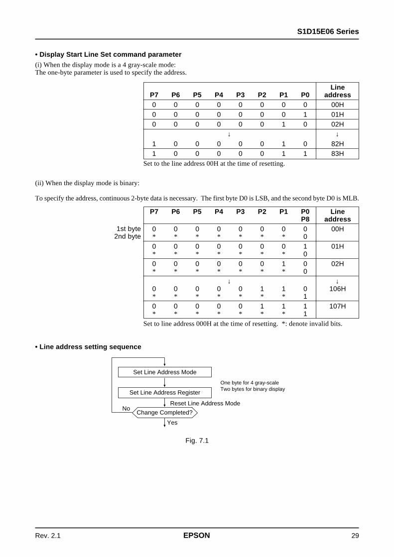
The parameter following this command specifies the display start line address of the display data RAM shown in Fig.6.5 and 6.6. When the Display Mode command is used to select 4 gray-scale display, a 1-byte parameter must be entered.When the binary display is selected, a 2-byte parameter must be entered.The display area is indicated in the direction where line address numbers are incremented, starting from the specifiedline address. If a dynamic change of the line address is made by this command, smooth scrolling in the longitudinaldirection and page breaking are enabled. For details, see the description of “6.2.4 Line address circuit” in the FunctionDescription.
E R/WA0 RD WR D7 D6 D5 D4 D3 D2 D1 D00 1 0 1 0 0 0 1 0 1 0 Mode setting1 1 0 P7 P6 P5 P4 P3 P2 P1 P0 Register setting 11 1 0 * * * * * * * P8 Register setting 2
(only binary display required)*: denote invalid bits.
S1D15E06 Series
Rev. 2.1 EPSON 29
LineP7 P6 P5 P4 P3 P2 P1 P0 address0 0 0 0 0 0 0 0 00H0 0 0 0 0 0 0 1 01H0 0 0 0 0 0 1 0 02H
↓ ↓1 0 0 0 0 0 1 0 82H1 0 0 0 0 0 1 1 83H
Set to the line address 00H at the time of resetting.
• Display Start Line Set command parameter
(i) When the display mode is a 4 gray-scale mode:The one-byte parameter is used to specify the address.
(ii) When the display mode is binary:
To specify the address, continuous 2-byte data is necessary. The first byte D0 is LSB, and the second byte D0 is MLB.
1st byte2nd byte
P7 P6 P5 P4 P3 P2 P1 P0 LineP8 address
0 0 0 0 0 0 0 0 00H* * * * * * * 00 0 0 0 0 0 0 1 01H* * * * * * * 00 0 0 0 0 0 1 0 02H* * * * * * * 0
↓ ↓0 0 0 0 0 1 1 0 106H* * * * * * * 10 0 0 0 0 1 1 1 107H* * * * * * * 1
Set to line address 000H at the time of resetting. *: denote invalid bits.
Fig. 7.1
• Line address setting sequence
Yes
NoChange Completed?
Set Line Address Register
Set Line Address Mode
Reset Line Address Mode
One byte for 4 gray-scaleTwo bytes for binary display

S1D15E06 Series
30 EPSON Rev. 2.1
(7) Page Address Set
This command specifies the page address corresponding to row address when MPU access to the display data RAMshown in Fig. 6.5 and 6.6. For details, see the description of “6.2.2 Page address circuit” in the Function Description.
E R/WA0 RD WR D7 D6 D5 D4 D3 D2 D1 D0 Page address0 1 0 1 0 1 1 0 0 0 1 Command1 1 0 * * P5 P4 P3 P2 P1 P0 Page address setting
*: denote invalid bits.
P5 P4 P3 P2 P1 P0 Page address0 0 0 0 0 0 00 0 0 0 0 1 1
↓ ↓0 1 1 1 1 1 311 0 0 0 0 0 32
(8) Column Address Set
This command sets the display data RAM column address given in Fig. 6.5 and 6.6. For details, see the description of“6.2.3 Column address circuit” in the Function Description.
E R/WA0 RD WR D7 D6 D5 D4 D3 D2 D1 D00 1 0 0 0 0 1 0 0 1 11 1 0 P7 P6 P5 P4 P3 P2 P1 P0
ColumnP7 P6 P5 P4 P3 P2 P1 P0 address0 0 0 0 0 0 0 0 00 0 0 0 0 0 0 1 10 0 0 0 0 0 1 0 2
↓ ↓1 0 0 0 0 0 1 0 1581 0 0 1 1 1 1 1 159
(9) Display Data Write
This command allows the 8-bit data to be written to the address specified by the display data RAM. After writing,column address or page address is automatically incremented +1 by the Display Data Input Direction Select command.This enables the MPU to write the display data continuously.
E R/WA0 RD WR D7 D6 D5 D4 D3 D2 D1 D00 1 0 0 0 0 1 1 1 0 11 1 0 Write Data

S1D15E06 Series
Rev. 2.1 EPSON 31
(10) Display Data Read
This command allows the 8-bit data to be read from the address specified by the display data RAM. After reading,column address or page address is automatically incremented +1 by the Display Data Input Direction select command.This enables the MPU to read multiple word data continuously.It should be noted that one dummy reading is essential immediately after the column address or page address has beenset. For details, see the description of “6.1.5 Access to display data RAM and internal register” in the FunctionDescription. When the serial interface is used, display data cannot be read.
E R/WA0 RD WR D7 D6 D5 D4 D3 D2 D1 D00 1 0 0 0 0 1 1 1 0 01 0 1 Read Data
(11) Display Data Input Direction Select
This command sets the direction where the display RAM address number is automatically incremented. For details,see the description of “6.2.3 Column address circuit” in the Function Description.
E R/WA0 RD WR D7 D6 D5 D4 D3 D2 D1 D0 Direction0 1 0 1 0 0 0 0 1 0 0 Column
1 Page
(12) Column Address Set Direction
This command can reverse the relationship between the display RAM data column address and segment driver outputshown in Fig. 6.5 and 6.6. So you can reverse the sequence of segment driver output pins using this command. Whenthe display data is written or read, the column address is incremented by (+1) according to the column address givenin Fig. 6.4 and 6.5. For details, see the description of “6.2.3 Column address circuit” in the Function Description.
(13) n-line Inversion Drive Register Set
This command sets the liquid crystal alternating drive reverse line count in the register to start line reverse drivingoperation. The line count to be set is 4 to 128 (32 states for each 4 lines. For details, see the description of “6.4 Displaytiming generation circuit” in the Function Description.
E R/WA0 RD WR D7 D6 D5 D4 D3 D2 D1 D0 Setting0 1 0 1 0 1 0 0 0 0 0 Normal
1 Reverse
E R/WA0 RD WR D7 D6 D5 D4 D3 D2 D1 D0 Reverse line count0 1 0 0 0 1 1 0 1 1 0 Command1 1 0 * * * P4 P3 P2 P1 P0 Reverse line count
*: denote invalid bits.
P4 P3 P2 P1 P0 Reverse line count0 0 0 0 0 4 (1 × 4)0 0 0 0 1 8 (2 × 4)
↓ ↓1 1 1 1 0 124 (31 × 4)1 1 1 1 1 128 (32 × 4)
S1D15E06 Series
32 EPSON Rev. 2.1
E R/WA0 RD WR D7 D6 D5 D4 D3 D2 D1 D0 n-line0 1 0 1 1 1 0 0 1 0 0 OFF
1 ON
(14) n-line ON/OFF
This command provides ON/OFF control of n-line inverting drive.
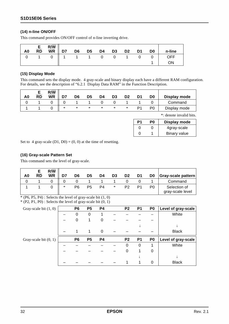
(16) Gray-scale Pattern Set
This command sets the level of gray-scale.
E R/WA0 RD WR D7 D6 D5 D4 D3 D2 D1 D0 Gray-scale pattern0 1 0 0 0 1 1 1 0 0 1 Command1 1 0 * P6 P5 P4 * P2 P1 P0 Selection of
gray-scale level* (P6, P5, P4) : Selects the level of gray-scale bit (1, 0)* (P2, P1, P0) : Selects the level of gray-scale bit (0, 1)
Gray-scale bit (1, 0) P6 P5 P4 P2 P1 P0 Level of gray-scale– 0 0 1 – – – – White– 0 1 0 – – – –
↓ ↓– 1 1 0 – – – – Black
Gray-scale bit (0, 1) P6 P5 P4 P2 P1 P0 Level of gray-scale– – – – – 0 0 1 White– – – – – 0 1 0
↓ ↓– – – – – 1 1 0 Black
(15) Display Mode
This command sets the display mode. 4 gray-scale and binary display each have a different RAM configuration.For details, see the description of “6.2.1 Display Data RAM” in the Function Description.
Set to 4 gray-scale (D1, D0) = (0, 0) at the time of resetting.
E R/WA0 RD WR D7 D6 D5 D4 D3 D2 D1 D0 Display mode0 1 0 0 1 1 0 0 1 1 0 Command1 1 0 * * * * * * P1 P0 Display mode
*: denote invalid bits.
P1 P0 Display mode0 0 4gray-scale0 1 Binary value

S1D15E06 Series
Rev. 2.1 EPSON 33
(17) Area Scroll Set
This command sets the area scroll. When the binary display is selected by the Display Mode Set command, the scrollend line address becomes a two-byte parameter.
1 4 gray-scale display
E R/WA0 RD WR D7 D6 D5 D4 D3 D2 D1 D0 Area scroll0 1 0 0 0 0 1 0 0 0 0 Command1 1 0 * * * * * * P11 P10 Scroll mode1 1 0 P27 P26 P25 P24 P23 P22 P21 P20 Scroll start line address1 1 0 P37 P36 P35 P34 P33 P32 P31 P30 Scroll end line address1 1 0 P47 P46 P45 P44 P43 P42 P41 P40 Scroll display line count
*: denote invalid bits.
P11 P10 Scroll mode0 0 0 (full screen)0 1 1 (Upper)1 0 2 (Lower)1 1 3 (Central)
P27 P26 P25 P24 P23 P22 P21 P20 Scroll start line address0 0 0 0 0 0 0 0 00H0 0 0 0 0 0 0 1 01H
↓ ↓1 0 0 0 0 0 1 0 82H1 0 0 0 0 0 1 1 83H
P37 P36 P35 P34 P33 P32 P31 P30 Scroll end line address0 0 0 0 0 0 0 0 00H0 0 0 0 0 0 0 1 01H
↓ ↓1 0 0 0 0 0 1 0 82H1 0 0 0 0 0 1 1 83H
P47 P46 P45 P44 P43 P42 P41 P40 Scroll display line count0 0 0 0 0 0 0 1 10 0 0 0 0 0 1 0 2
↓ ↓1 0 0 0 0 0 1 1 1311 0 0 0 0 1 0 0 132

S1D15E06 Series
34 EPSON Rev. 2.1
2 Binary display
E R/WA0 RD WR D7 D6 D5 D4 D3 D2 D1 D0 Area scroll0 1 0 0 0 0 1 0 0 0 0 Command1 1 0 * * * * * * P11 P10 Scroll mode1 1 0 P27 P26 P25 P24 P23 P22 P21 P20 Scroll start line address1 1 0 P37 P36 P35 P34 P33 P32 P31 P30 Scroll end line address1 1 0 * * * * * * * P381 1 0 P47 P46 P45 P44 P43 P42 P41 P40 Scroll display line count
*: denote invalid bits.
• Specifications on the parameters for scroll mode, scroll start line address and scroll display line count are the sameas those on 4 gray-scale display.
P37 P36 P35 P34 P33 P32 P31 P30 Scroll end line addressP38 Binary value
0 0 0 0 0 0 0 0 00H* * * * * * * 00 0 0 0 0 0 0 1 01H* * * * * * * 0
↓ ↓0 0 0 0 0 1 1 0 106H* * * * * * * 10 0 0 0 0 1 1 1 107H* * * * * * * 1
1st byte2nd byte
(18) Duty Set Command
Liquid crystal drive at a lower power consumption is ensured by using this command to change the duty. Use of thiscommand also allows display at a desired position on the panel (continuous COM pins on a 4-line basis).This command is used with a pair of the duty set parameter and start point (block) parameter, so be sure to set bothparameters so that one of them will immediately follow the other.
E R/WA0 RD WR D7 D6 D5 D4 D3 D2 D1 D0 Selected state0 1 0 0 1 1 0 1 1 0 1 Duty set command1 1 0 * * P15 P14 P13 P12 P11 P10 Duty set1 1 0 * * P25 P24 P23 P22 P21 P20 Start point set
*: denote invalid bits.
• Duty set
Duty can be set in the range from 1/4 duty to 1/132 duty by 4 steps.Set to 1/132 duty after resetting.
P15 P14 P13 P12 P11 P10 Duty set0 0 0 0 0 0 1/4 duty set0 0 0 0 0 1 1/8 duty set0 0 0 0 1 0 1/12 duty set0 0 0 0 1 1 1/16 duty set
↓ ↓0 1 1 1 1 1 1/128 duty set1 0 0 0 0 0 1/132 duty set
S1D15E06 Series
Rev. 2.1 EPSON 35
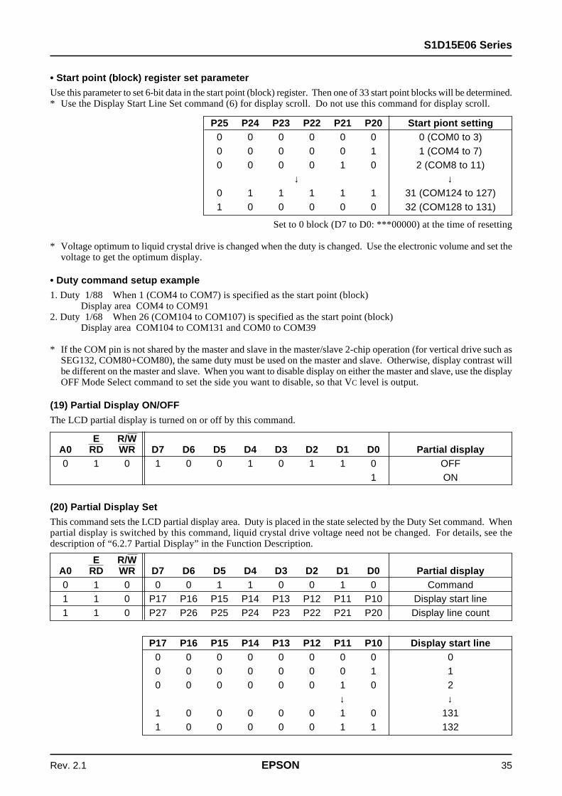
• Start point (block) register set parameter
Use this parameter to set 6-bit data in the start point (block) register. Then one of 33 start point blocks will be determined.* Use the Display Start Line Set command (6) for display scroll. Do not use this command for display scroll.
Set to 0 block (D7 to D0: ***00000) at the time of resetting
* Voltage optimum to liquid crystal drive is changed when the duty is changed. Use the electronic volume and set thevoltage to get the optimum display.
• Duty command setup example
1. Duty 1/88 When 1 (COM4 to COM7) is specified as the start point (block)Display area COM4 to COM91
2. Duty 1/68 When 26 (COM104 to COM107) is specified as the start point (block)Display area COM104 to COM131 and COM0 to COM39
* If the COM pin is not shared by the master and slave in the master/slave 2-chip operation (for vertical drive such asSEG132, COM80+COM80), the same duty must be used on the master and slave. Otherwise, display contrast willbe different on the master and slave. When you want to disable display on either the master and slave, use the displayOFF Mode Select command to set the side you want to disable, so that VC level is output.
(19) Partial Display ON/OFF
The LCD partial display is turned on or off by this command.
P25 P24 P23 P22 P21 P20 Start piont setting0 0 0 0 0 0 0 (COM0 to 3)0 0 0 0 0 1 1 (COM4 to 7)0 0 0 0 1 0 2 (COM8 to 11)
↓ ↓0 1 1 1 1 1 31 (COM124 to 127)1 0 0 0 0 0 32 (COM128 to 131)
E R/WA0 RD WR D7 D6 D5 D4 D3 D2 D1 D0 Partial display0 1 0 1 0 0 1 0 1 1 0 OFF
1 ON
(20) Partial Display Set
This command sets the LCD partial display area. Duty is placed in the state selected by the Duty Set command. Whenpartial display is switched by this command, liquid crystal drive voltage need not be changed. For details, see thedescription of “6.2.7 Partial Display” in the Function Description.
P17 P16 P15 P14 P13 P12 P11 P10 Display start line0 0 0 0 0 0 0 0 00 0 0 0 0 0 0 1 10 0 0 0 0 0 1 0 2
↓ ↓1 0 0 0 0 0 1 0 1311 0 0 0 0 0 1 1 132
E R/WA0 RD WR D7 D6 D5 D4 D3 D2 D1 D0 Partial display0 1 0 0 0 1 1 0 0 1 0 Command1 1 0 P17 P16 P15 P14 P13 P12 P11 P10 Display start line1 1 0 P27 P26 P25 P24 P23 P22 P21 P20 Display line count

S1D15E06 Series
36 EPSON Rev. 2.1
* The result of display start line added to display line count exceeding 132 should be disregarded.
(21) Read Modify Write
This command is paired with end command for use. If this command is entered, the column address is not changed bythe Display Data Read command. It can be incremented +1 by the Display Data Read command alone. This state sretained until the End command is input. If the End command is input, the column address goes back to the addresswhen the Read Modify Write command is input. This function reduces the MPU loads when changing the data repeatedin the specific display area such as blinking cursor.
* A command other than display data Read/Write command can be used in the Read Modify Write mode. However,you cannot use the column address set command.
• Sequence for cursor display
P17 P16 P15 P14 P13 P12 P11 P10 Display start line0 0 0 0 0 0 0 1 10 0 0 0 0 0 1 0 2
↓ ↓1 0 0 0 0 0 1 1 1311 0 0 0 0 1 0 0 132
E R/WA0 RD WR D7 D6 D5 D4 D3 D2 D1 D00 1 0 1 1 1 0 0 0 0 0
Fig. 7.2
Page Address Set
Column Address Set
Dummy Read
Data Read
Data Write
End
Yes
NoChange Completed?
Read Modify Write
Data Manipulation

S1D15E06 Series
Rev. 2.1 EPSON 37
(22) End
This command releases the read modify write mode and gets column address back to the initial address of the mode.
Fig. 7.3
(23) Built-in Oscillator Circuit ON/OFF
This command starts the built-in oscillator circuit operation. It is enabled only in the master operation mode (M/S =HIGH) when built-in oscillator circuit is valid (CLS = HIGH).When the built-in power supply is used, the Oscillator Circuit ON command must be executed before the Power ControlSet command. (See the description of “(16) power control command”). If the built-in oscillator circuit is turned offwhen the built-in power supply is used, display failure may occur.
E R/W Built-in oscillatorA0 RD WR D7 D6 D5 D4 D3 D2 D1 D0 circuit0 1 0 1 0 1 0 1 0 1 0 OFF
1 ON
E R/WA0 RD WR D7 D6 D5 D4 D3 D2 D1 D00 1 0 1 1 1 0 1 1 1 0
NN+m• • •N+3N+2N+1NColumn address
Set read-modify-write mode End
Return

S1D15E06 Series
38 EPSON Rev. 2.1
(24) Built-in Oscillator Circuit Frequency Select
This command sets the built-in oscillator circuit frequency. The frequency can be selected whether the built-in oscillatorcircuit is turned on or off.
E R/WA0 RD WR D7 D6 D5 D4 D3 D2 D1 D0 fOSC kHz fCL kHz0 1 0 0 1 0 1 1 1 1 1 Command Command1 1 0 * * * * P3 P2 P1 P0 Oscillation CL frequency
frequency
Oscillation CL frequencyfrequency fCL kHz
P3 P2 P1 P0 fOSC kHz0 0 0 0 120.0 fOSC 120.00 0 0 1 100.0 fOSC 100.00 0 1 0 88.0 fOSC 88.00 0 1 1 76.0 fOSC 76.00 1 0 0 120.0 fOSC/2 = 60.00 1 0 1 100.0 fOSC/2 = 50.00 1 1 0 88.0 fOSC/2 = 44.00 1 1 1 76.0 fOSC/2 = 38.01 0 0 0 120.0 fOSC/4 = 30.01 0 0 1 100.0 fOSC/4 = 25.01 0 1 0 88.0 fOSC/4 = 22.01 0 1 1 76.0 fOSC/4 = 19.01 1 0 0 120.0 fOSC/8 = 15.01 1 0 1 100.0 fOSC/8 = 12.51 1 1 0 88.0 fOSC/8 = 11.01 1 1 1 76.0 fOSC/8 = 9.5
(D7 to D0: ****0000) is set after resetting.
* The above-mentioned value is a Typ. value at 25°C. There is a tolerance of ±12% at 25°C.

S1D15E06 Series
Rev. 2.1 EPSON 39
E R/WA0 RD WR D7 D6 D5 D4 D3 D2 D1 D0 Selected state0 1 0 0 0 1 0 0 1 0 1 Command1 1 0 0 0 0 P4 P3 P2 P1 P0 Register set
(25) Power Control Set
This command sets the built-in power supply circuit function. For details, see the description of “6.7 Power supplycircuit” in the Function Description.
P4 P3 P2 P1 P0 Selected state1 1 Triple step-up1 0 Double step-up0 1 VOUT = VDD
0 Step-up: OFF1 Step-up: ON
0 VC: OFF1 VC: ON
0 LCD voltage: OFF1 LCD voltage: ON
S1D15E06D00B*: (LCD voltage: V2, V1, MV1)S1D15E06D00B*: (LCD voltage: V3, V2, V1, MV1, MV2)
An internal clock is required to operate the built-in power supply circuit. During the operation of the built-in powersupply circuit, be sure that the internal clock is present inside.If the built-in oscillator circuit is used, execute the built-in oscillator circuit ON command before the power controlset command. If an external oscillator circuit is used, operate the external oscillator circuit before the power controlset command.If the internal clock is cut off during the operation of the built-in power supply circuit, display failure may occur. Toavoid this, do not cut it off.In the slave operation mode, only the parameters (D7 to D0 : ***00000) can be used with the power control setcommand. Do not use any other parameter.100ms or more should be kept from VC regulator circuit ON to LCDV circuit ON.
Fig. 7.4
Power Control Set 1. Step-up circuit ON 2. VC regulator circuit ON 3. LCDV circuit ON*
Built-in oscillator ON External oscillator input
A built-in oscillator used An external oscillator used

S1D15E06 Series
40 EPSON Rev. 2.1
(26) Step-up CK Frequency Select
This command selects the step-up CK and step-down CK frequencies.
E R/WA0 RD WR D7 D6 D5 D4 D3 D2 D1 D00 1 0 0 1 0 0 0 0 0 1 Command1 1 0 * P6 P5 P4 * P2 P1 P0 Register
*: denote invalid bits.
(fosc/32) is set after resetting.
Step-up CK P6 P5 P4 P2 P1 P0 Step-up CK– – – – – 0 1 1 fOSC/8– – – – – 1 0 0 fOSC/16– – – – – 1 0 1 fOSC/32
↓ 1 1 0 fOSC/64– – – – – 1 1 1 fOSC/128
It should not use the following. (P2, P1, P0) = (0, 0, 0) , (0, 0, 1) , (0, 1, 0)
Step-down CK * P6 P5 P4 *000 P2 P1 P0 Step-down CK– 0 1 1 – – – – fOSC/8– 1 0 0 – – – – fOSC/16– 1 0 1 – – – – fOSC/32
1 1 0 ↓ fOSC/64– 1 1 1 – – – – fOSC/128
It should not use the following. (P6, P5, P4) = (0, 0, 0) , (0, 0, 1) , (0, 1, 0)* For S1D15E06D00B*, the step-down CK register is disabled.
(27) Liquid Crystal Drive Voltage Select
The liquid crystal drive voltage range issued from the liquid crystal drive voltage regulating circuit is selected from 3states by this command.
E R/W VC voltageA0 RD WR D7 D6 D5 D4 D3 D2 D1 D0 output range0 1 0 0 0 1 0 1 0 1 1 Command1 1 0 * * * * * * P1 P0 Register
*: denote invalid bits.
VC voltageP1 P0 output range0 0 1.77 to 3.50 V1 0 2.53 to 5.00 V1 1 3.54 to 7.00 V
VC voltage output range, 1.77 to 3.50V, (D1, D0) = (0, 0) is set after resetting.
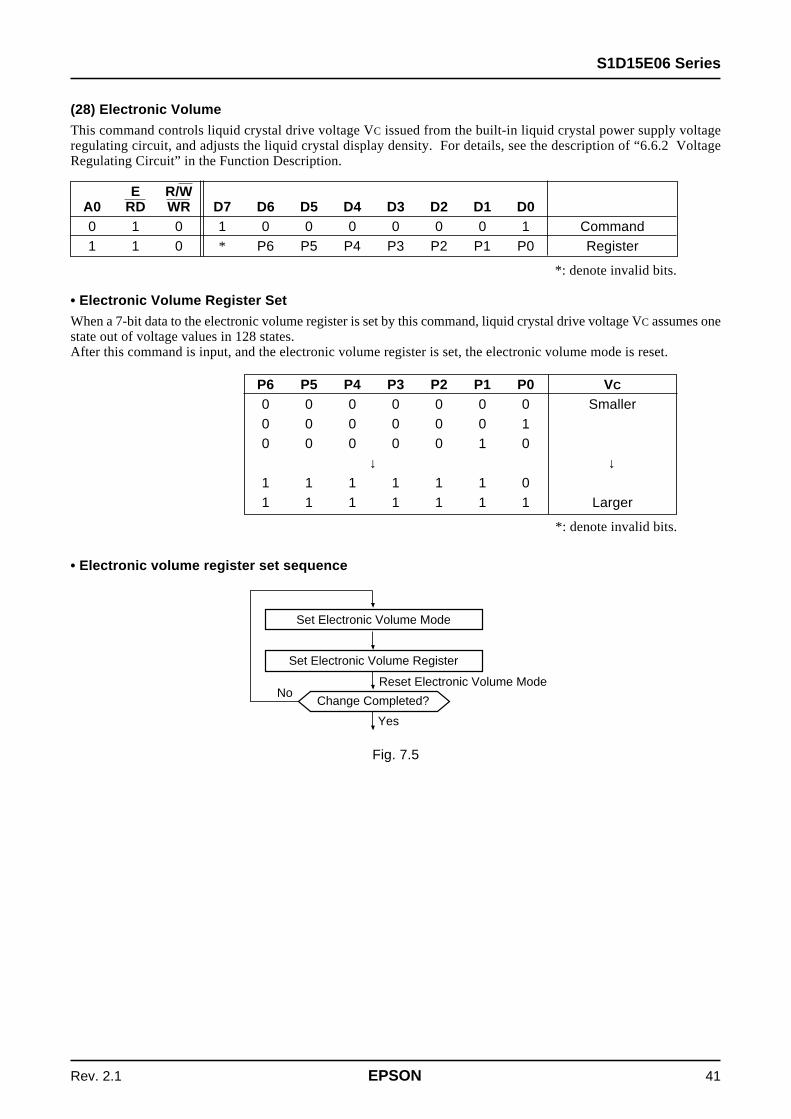
S1D15E06 Series
Rev. 2.1 EPSON 41
(28) Electronic Volume
This command controls liquid crystal drive voltage VC issued from the built-in liquid crystal power supply voltageregulating circuit, and adjusts the liquid crystal display density. For details, see the description of “6.6.2 VoltageRegulating Circuit” in the Function Description.
• Electronic Volume Register Set
When a 7-bit data to the electronic volume register is set by this command, liquid crystal drive voltage VC assumes onestate out of voltage values in 128 states.After this command is input, and the electronic volume register is set, the electronic volume mode is reset.
• Electronic volume register set sequence
E R/WA0 RD WR D7 D6 D5 D4 D3 D2 D1 D00 1 0 1 0 0 0 0 0 0 1 Command1 1 0 * P6 P5 P4 P3 P2 P1 P0 Register
*: denote invalid bits.
Fig. 7.5
P6 P5 P4 P3 P2 P1 P0 VC
0 0 0 0 0 0 0 Smaller0 0 0 0 0 0 10 0 0 0 0 1 0
↓ ↓1 1 1 1 1 1 01 1 1 1 1 1 1 Larger
*: denote invalid bits.
Yes
NoChange Completed?
Set Electronic Volume Register
Set Electronic Volume Mode
Reset Electronic Volume Mode

S1D15E06 Series
42 EPSON Rev. 2.1
(29) Discharge ON/OFF
This command discharges the capacitors connected to the power supply circuit. This command is used when the systempower of this IC (S1D15E06 series) is turned off, and the duty is changed. See the description of (3) Power Supply OFFand (4) Changing the Duty in the Instruction Setup: Reference.
* If this command is executed when the external power supply is used, a large current may flow to damage the IC. Ifexternal power supply is used to drive liquid crystal, be sure to turn off the external power supply before executingthis command.
(30) Power Saving
This command establishes the power save mode, thereby ensuring a substantial reduction of current consumption.
E R/WA0 RD WR D7 D6 D5 D4 D3 D2 D1 D0 Setting0 1 0 1 1 1 0 1 0 1 0 Discharge OFF
1 Discharge ON
In the power save mode, display data and operation before power saving are maintained. Access to the display dataRAM from the MPU is also possible. The current consumption is reduced to the value close to static current if alloperations of the LCD display system are stopped and there is no access from the MPU.
In the power save mode, the following occurs:Stop of oscillator circuitStop of LCD power supply circuitStop of all liquid crystal drive circuit (VSS level output is issued as the segment and common driver output).
The power save OFF command releases the power save mode. The system goes back to the state before the power savemode.
* When the external power supply is used, it is recommended to stop the external power supply circuit function whenthe power save mode is started. For example, when each level of the liquid crystal drive voltage is given from theexternal resistive divider circuit, it is recommended to add a circuit to cut off the current flowing to the resistivedivider circuit when power save function is started. The S1D15E06 series has a liquid crystal display blankingcontrol control pin DOF, and the level goes LOW when power save function is started. You can use the DOF outputto stop the external power supply circuit function.
E R/WA0 RD WR D7 D6 D5 D4 D3 D2 D1 D0 Power save mode0 1 0 1 0 1 0 1 0 0 0 OFF
1 ON

S1D15E06 Series
Rev. 2.1 EPSON 43
(31) Temperature Gradient Set
The 3-bit data of this command is used to set the temperature gradient characteristics of the liquid crystal drive voltageoutput from the built-in power supply circuit from eight states to one state. The temperature gradient of the liquid crystaldrive voltage can be set according to the liquid crystal temperature gradient to be used. This eliminates the need of atemperature characteristics regulating circuit to be installed outside this IC (S1D15E06 series).
E R/W TemperatureA0 RD WR D7 D6 D5 D4 D3 D2 D1 D0 gradient [%/°C]0 1 0 0 1 0 0 1 1 1 0 Command1 1 0 * * * * * P2 P1 P0 Register
*: denote invalid bits.
(32) Status Read
This command reads out the temperature gradient select bit set on the register.
TemperatureP2 P1 P0 gradient [%/°C]0 0 0 –0.060 0 1 –0.080 1 0 –0.100 1 1 –0.111 0 0 –0.131 0 1 –0.151 1 0 –0.171 1 1 –0.18
(D7 to D0: *****000) is set after resetting. *: denote invalid bits.
E R/W TemperatureA0 RD WR D7 D6 D5 D4 D3 D2 D1 D0 gradient [%/°C]0 1 0 1 0 0 0 1 1 1 0 Command1 0 1 * * * * * P2 P1 P0 Register
*: denote invalid bits.
TemperatureP2 P1 P0 gradient [%/°C]0 0 0 –0.061 0 0 –0.080 1 0 –0.101 1 0 –0.110 0 1 –0.131 0 1 –0.150 1 1 –0.171 1 1 –0.18

S1D15E06 Series
44 EPSON Rev. 2.1
(33) Reset
This command resets the column address, page address, read modify write mode and test mode without giving adverseeffect to the display data RAM. For details, see the description of “6.8 Reset” in Function Description. Resetting iscarried out after the reset command has been input.
Initialization upon application of power supply is carried out by the reset signal to the RES pin. The reset commandcannot be used for this purpose.
(34) MLS drive selection command
These are the MLS drive selection commands. These commands changes over between the dispersive drive andnondispersive drive.
* indicates the invalid bits.
After resetting, nondispersive drive will be preset in 4 gradation indications.In case the B/W indication is selected after resetting, dispersive drive will be preset.
Dispersive drive and nondispersive drive are the LCD drive methods characteristic to the MLS drive.The S1D15E06 Series is making 4 line MLS drive and, 4 times higher period selection voltage than that of the periodbeing used for indication of 1 line in an ordinary drive (in case of 132 line indication, the period of 1/132 of 1 frame).In case of the dispersive drive, the selection signals will be output for four times, separately, within the period of 1 frame.With this dispersive drive method, it is possible to reduce the frame frequency as compared with the nondispersive drivemethod. Therefore, when it becomes necessary to reduce the current consumption, we recommend you to use this divemethod. However, in case of the drive method where moving pictures are to be indicated, the indication may becomeflickered and this dispersive drive method is not suitable for indications of moving pictures.
(35) NOP
This is a Non-Operation command.
Note: S1D15E06 series maintains the operation status due to the command. However, when exposed to excessiveexternal noise, internal status may be changed. This makes it necessary to take some measures which reducesnoise generation in terms of installation or system configuration, or which protects the system against adverseeffect of noise. To cope with sudden noise, it is recommended to refresh the operation status on a periodic basis.
E R/WA0 RD WR D7 D6 D5 D4 D3 D2 D1 D00 1 0 1 1 1 0 0 0 1 0
E R/WA0 RD WR D7 D6 D5 D4 D3 D2 D1 D00 1 0 1 1 1 0 0 0 1 1
E R/W Temperature gradientA0 RD WR D7 D6 D5 D4 D3 D2 D1 D0 [%/˚C]0 1 0 1 0 0 1 1 1 0 0 Command1 1 0 * * * * P3 P2 P1 P0 Register
Temperature gradientP3 P2 P1 P0 [%/˚C]0 0 0 0 Dispersive drive1 0 0 0 Nondispersive drive

S1D15E06 Series
Rev. 2.1 EPSON 45
Command code
Command A0 RD WR D7 D6 D5 D4 D3 D2 D1 D0 Function(1) Display ON/OFF 0 1 0 1 0 1 0 1 1 1 0 LCD display ON/OFF control.
1 0: OFF, 1: ON(2) Display OFF Mode 0 1 0 1 0 1 1 1 1 1 0 Output level when the display is OFF and in
Select 1 the power save mode 0: VSS, 1: VC
(3) Display Normal 0 1 0 1 0 1 0 0 1 1 0 LCD display normal/reverse/Reverse 1 0: Normal, 1: Reverse
(4) Display All Lighting 0 1 0 1 0 1 0 0 1 0 0 Display All LightingON/OFF 1 0: Normal display, 1: All ON
(5) Common Output 0 1 0 1 1 0 0 0 1 0 0 Selects COM output scan direction.Status Select 1 0: Normal, 1: Reverse
(6) Display Start Line Set 0 1 0 1 0 0 0 1 0 1 0 Sets display start line.1 1 0 Display start line address When the display mode is binary,1 1 0 * * * * * * * ↓ the parameter consists of two bytes.
(7) Page Address Set 0 1 0 1 0 1 1 0 0 0 1 Sets the display RAM page address.* * Page address
(8) Column Address Set 0 1 0 0 0 0 1 0 0 1 1 Sets the display RAM column1 1 0 Column Address Set address.
(9) Display Data Write 0 1 0 0 0 0 1 1 1 0 1 Writes data to the display RAM.1 1 0 Writes data
(10) Display Data Read 0 1 0 0 0 0 1 1 1 0 0 Reads data to the display RAM.1 0 1 Reads data
(11) Display Data Input 0 1 0 1 0 0 0 0 1 0 0 Display RAM data input directionDirection Select 1 0: Column direction 1: Page direction
(12) Column Address Set 0 1 0 1 0 1 0 0 0 0 0 Compatible with display RAMDirection 1 address SEG output
0: Normal 1: Reverse(13) N-line inversion Drive 0 1 0 0 0 1 1 0 1 1 0 Line invert drive.
Register Set 1 1 0 * * * Invert line count Sets the line count.(14) N-line ON/OFF 0 1 0 1 1 1 0 0 1 0 0 Resets the line invert drive.
1 0: N-line OFF 1: N-line ON(15) Display Mode 0 1 0 0 1 1 0 0 1 1 0 00: 4 gray-scale, 01: binary
1 1 0 * * * * * * Mode(16) Gray-scale Pattern Set 0 1 0 0 0 1 1 1 0 0 1 Selects the contrast of gray-scale
1 1 0 Gray-scale pattern bit (1,0) (0,1).(17) Area Scroll 0 1 0 0 0 0 1 0 0 0 0
Scroll Mode 1 1 0 * * * * * * Mode When the display mode is binary,Scroll Start address 1 1 0 Start address the end address consists ofScroll End address 1 1 0 End address two bytes.Display page count 1 1 0 Display page count
(18) Duty Set Command 0 1 0 0 1 1 0 1 1 0 1Duty Set * * Duty countStatic spot (block) set * * Static spot (block)
(19) Partial Display 0 1 0 1 0 0 1 0 1 1 0 Partial display ON/OFFON/OFF 1 0: OFF, 1: ON
(20) Partial Display Set 0 1 0 0 0 1 1 0 0 1 0Display Start line Start lineDisplay Line count Line count
(21) Read Modify Write 0 1 0 1 1 1 0 0 0 0 0 Increments the column address.Increments +1 in the write mode.Does not increment in the read mode.
(22) End 0 1 0 1 1 1 0 1 1 1 0 Resets read modify write functions.(23) Built-in Oscillator 0 1 0 1 0 1 0 1 0 1 0 Built-in oscillator circuit operation
Circuit ON/OFF 1 0: OFF, 1: ON(24) Built-in Oscillator 0 1 0 0 1 0 1 1 1 1 1
Circuit Frequency Select 1 1 0 * * * * Frequency(25) Power Control Set 0 1 0 0 0 1 0 0 1 0 1 Selects built-in power supply
1 1 0 * * Operation state operation state.
Table 7.1 Table of commands in S1D15E06 series

S1D15E06 Series
46 EPSON Rev. 2.1
Command code
Command A0 RD WR D7 D6 D5 D4 D3 D2 D1 D0 Function(26) Step-up CK 0 1 0 0 1 0 0 0 0 0 1
Frequency Select 1 1 0 * Frequency(27) Liquid Crystal Drive 0 1 0 0 0 1 0 1 0 1 1
Voltage Select 1 1 0 * * * * * * VC range(28) Electronic Volume 0 1 0 1 0 0 0 0 0 0 1
Mode SetElectronic Volume 1 1 0 * Electronic volume VC output voltage is set to theRegister Set electronic volume register. 128 states
(29) Discharge ON/OFF 0 1 0 1 1 1 0 1 0 1 0 Discharges Power supply circuit1 connection capacitor.
0: OFF (normal), 1: ON(30) Power Save ON/OFF 0 1 0 1 0 1 0 1 0 0 0 Power Save 0: OFF, 1: ON(31) Temperature 0 1 0 0 1 0 0 1 1 1 0 Sets to 8 steps.
Gradient Select 1 1 0 * * * * * Temperature gradient(32) Stator Read 0 1 0 1 0 0 0 1 1 1 0 Issues the temperature gradient
1 0 1 * * * * *Temperature gradient select bit.(33) Reset 0 1 0 1 1 1 0 0 0 1 0 Resets the column, page and
address registers.Resets the readmodify write function.
(34) MLS drive selection 0 1 0 1 0 0 1 1 1 0 0 MLS drive method1 1 0 * * * * MLS drive method 0 : Dispersive, 1 : Nondispersive
(35) NOP 0 1 0 1 1 1 0 0 0 1 1 Non-operation command

S1D15E06 Series
Rev. 2.1 EPSON 47
Stable power supply
*1
VDD - VSS power turns on when RES terminal = LOW.
Release the reset state. (RES terminal = HIGH)
Function setup by command entry (set by users) (12) Column address set direction (5) Common output status select (3) Display normal/reverse (4) Display all lighting ON/OFF (18) Set the duty (2) Display OFF mode select (27) LCD voltage select (28) Electronic volume (31) Temperature gradient set
Initialization completed
Function setup by command entry (set by users) (13) n-line invert drive register set (14) n-line ON/OFF
Function setup by command entry (set by users) (24) Built-in oscillator circuit frequency select (23) Built-in oscillator circuit ON/OFF
Function setup by command entry (set by users) (25) Power control set 1. Step-up circuit ON 2. VC regulator circuit ON 3. LCDV circuit ON*2
(When the n-line invert drive is not used)
(When the external oscillator circuit is used)
(When the external LCD power supply circuit is used)
Enter the external clock
External LCD power supply entry
Instruction Setup Example (Reference)(1) Initial setup
Note: *1 Display data RAM contents are not determined even in the initialized state after resetting. See “6.7 ResetCircuit” in the “6. Function Description”.
*2 100ms or more should be kept from VC regulator circuit ON to LCDV circuit ON.* Numerals in the command parenthesis correspond to the numerals of the items in Command Description.

S1D15E06 Series
48 EPSON Rev. 2.1
End of initialization
End of data display
Function setup by command entry (set by users) (6) Display start line set (7) Page address set (8) Column address set
Function setup by command entry (set by users) (9) Display data write
Function setup by command entry (set by users) (1) Display ON/OFF command
A desired state
VDD - VSS power supply OFF
Function setup by command entry (set by users) (30) Power save ON
Function setup by command entry (set by users) (29) Discharge ON/OFF
External LCD power supply OFF
(When an external LCD power supply circuit is used)
Reset state (RES terminal = LOW)
(When the built-in power supply circuit is used)
Set the time (tL) between entry into the reset state and turning off of VDD-VSS power supply liquid crystal drive potential (MV1,VC,V1,V2) so that it is longer than the time (tH) where it is reduced below the threshold value of the LCD panel.
(2) Data display
Note: * Display data RAM contents are not determined after end of initialization. Write data to all the Display dataRAM used for display. See “9. Display data write” in the “7. Command Description”.
(3) Power OFF
Note: * This IC controls the circuit of the liquid crystal drive power supply system using the VDD-VSS power supplycircuit. If the VDD-VSS power supply is cut off with voltage remaining in the liquid crystal drive powersupply system, voltage not controlled will be issued from the SEG and COM pins, and this may result indisplay failure. To avoid this, follow the above-mentioned power off sequence.

S1D15E06 Series
Rev. 2.1 EPSON 49
Function setup by command entry (set by users)
(28) Electronic volume
(24) Built-in oscillator circuit frequency select
(18) Duty set
When the n-line reversing command is used :
(13) n-line reverse drive register set
Function setup by command entry (set by users)
(1) Displya OFF
Function setup by command entry (set by users)
(30) Power save ON
Function setup by command entry (set by users)
(29) Discharge ON
Function setup by command entry (set by users)
(29) Discharge OFF
Function setup by command entry (set by users)
(30) Power save OFF
A desired state
End of duty change
Secure an interval of
30ms or more between
discharge ON to
discharge OFF .
Note: * Execution of the above sequence causes display to be turned off temporarily (for the time from PowerSaving command ON to Power Saving command OFF plus 200 ms (frame frequency 60Hz) upon switchingof the duty. Temporary display failure may occur if Duty Change command is executed during liquidcrystal display without executing the above-mentioned setup example. Follow the setup example when theduty is changed as discussed above.
(5) Refresh
It is recommended that the operating modes and display contents be refreshed periodically to prevent the effect ofunexpected noise.
(4) How to change the duty
Set all commands to the ready state(Including default state setting.)
NOP command
Refresh sequence
Refreshing of DRAM

S1D15E06 Series
50 EPSON Rev. 2.1
Item Symbol Specified value UnitPower voltage (1) VDD –0.3 to +4.0 VPower voltage (2) V3, VOUT –0.3 to +17.0Power voltage (3) V2, V1, VC, MV1, MV2 –0.3 to V3
Input voltage VIN –0.3 to VDD+0.3Output voltage VO –0.3 to VDD+0.3Operating temperature TOPR –40 to +85 °CStorage temperature TCP TSTR –55 to +100
bare chip –55 to +125
System (MPU) side
VCC
GND
V2, V1,MV1,MV2
VDD
VOUT
VC
V3
VSS
S1D15E06 side
Table 8 VSS = 0V unless otherwise specified.
Fig. 8
Notes: 1. Voltages V3, V2, V1, VC, MV1, MV2 and MV3 (VSS) must always meet the conditions ofV3≥V2≥V1≥VC≥MV1≥MV2≥MV3 (VSS).
2. Voltage VOUT must always meet the conditions of VOUT≥VDD and VOUT≥VC.3. If the LSI has been used in excess of the absolute maximum rating, it may be subjected to permanent
breakdown. So in the normal operation, the LSI is preferred to be used under the condition of electricalcharacteristics. If this condition is not met, LSI operation error may occur and LSI reliability may bedeteriorated.
8. ABSOLUTE MAXIMUM RATINGS

S1D15E06 Series
Rev. 2.1 EPSON 51
Table 9.1
9. DC CHARACTERISTICSVSS = 0V, VDD = 2.7V ± 10% and Ta = –40 to +85°C unless otherwise specified.
Specified value ApplicableItem Symbol Conditions Min. Typ. Max. Unit pin
Working voltage (1) Operation enabled VDD 1.7 — 3.6 V VDD *1
Working voltage (2) Operation recommended VOUT VDD — 16.0 VOUT
Working voltage (3) Operation enabled V3 Applicable to 3.4 — 14.0 V3 *2Operation enabled VC S1D15E06D01**** 1.7 — 7.0 VC
Operation enabled V2 VC — V3 V2
Operation enabled V1 VC — V3 V1
Operation enabled MV1 VSS — VC MV1
Operation enabled MV2 VSS — VC MV2
Working voltage (4) Operation enabled V3 Applicable to 3.4 — 16.0 V3 *2Operation enabled VC S1D15E06D03**** 1.7 — 8.0 VC
Operation enabled V2 VC — V3 V2
Operation enabled V1 VC — V3 V1
Operation enabled MV1 VSS — VC MV1
Operation enabled MV2 VSS — VC MV2
High-level input voltage VIHC VDD=1.7V to 3.6V 0.8×VDD — VDD *3Low-level input voltage VILC VSS — 0.2×VDD *3
High-level output voltage VOHC VDD=1.7V IOH=–0.25mA 0.8×VDD — VDD *4Low-level output voltage VOLC to 3.6V IOL=0.25mA VSS — 0.2×VDD *4
Input leak current ILI VIN=VDD or VSS –1.0 — 1.0 µA *5Output leak current ILO –3.0 — 3.0 *6
LCD driver ON resistance RON Ta=25°C V3=7.2V — 1.5 2.3 kΩ SEGnV3=4.8V — 3.0 4.6 COMn *7
Static current consumption IDDQ Ta=25°C VDD=3.6V — 0.2 5.0 µA VDD
I3Q V3=14.0V — 1.0 5.0 V3
Input pin capacity CIN Ta=25°C, f=1MHz — 20 25 pF
Oscillation Built-in oscillation fOSC Ta=25°C 110 120 130 kHz *8frequency Max. frequency
[* See the description on P.57.]

S1D15E06 Series
52 EPSON Rev. 2.1
Display mode in 4 gray-scale at fFR = 80Hz
Table 9.4 Display: Heavy load display Code: ISS (1)
Display mode in binary at fFR = 60Hz
Table 9.5 Display entirely in white Code: ISS (1)
VDD Boosting V3 Voltage1/132 DUTY 1/100 DUTY
Unit RemarksTyp. Max. Typ. Max.
2.7V Triple 10V 241 400 187 310 µA *10
12V 373 619 313 519
3.6V Double 10V 189 313 146 242
Triple 12V 380 630 314 521
VDD Boosting V3 Voltage1/132 DUTY 1/100 DUTY
Unit RemarksTyp. Max. Typ. Max.
2.7V Triple 10V 65 108 50 83 µA *10
12V 72 120 56 93
3.6V Double 10V 57 95 44 73
Triple 12V 82 136 63 104
[* See the description on P.57.]
Table 9.2
Specified value ApplicableItem Symbol Conditions Min. Typ. Max. Unit pin
Input voltage VDD Double boosting 1.7 — 3.6 V VDD
VDD Triple boosting 1.7 — 3.6
Boosted output voltage (1) VOUT S1D15E06D01**** — — 14.0 VOUT
Boosted output voltage (2) VOUT S1D15E06D03**** — — 16.0 VOUT
Working voltage for voltage VC 1.8 — 8.0 VC *9control circuit
Bui
lt-in
pow
erci
rcui
t
Dynamic current consumption (1): Built-in power is turned on during display. Ta=25°CThis is the current consumed by the entire IC including the built-in power supply.
Display mode in 4 gray-scale at fFR = 80Hz
Table 9.3 Display entirely in white Code: ISS (1)
VDD Boosting V3 Voltage1/132 DUTY 1/100 DUTY
Unit RemarksTyp. Max. Typ. Max.
2.7V Triple 10V 68 112 67 111 µA *10
12V 81 134 71 117
3.6V Double 10V 73 121 63 104
Triple 12V 93 154 83 137
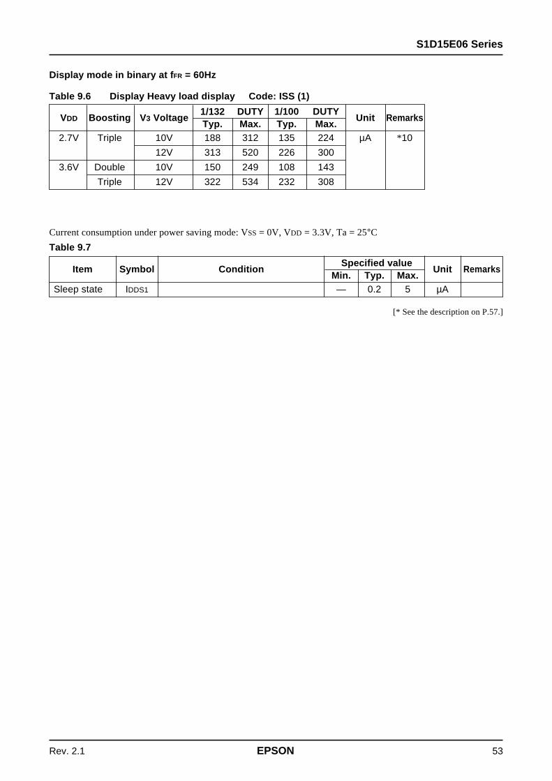
S1D15E06 Series
Rev. 2.1 EPSON 53
Table 9.7
Item Symbol ConditionSpecified value
Unit RemarksMin. Typ. Max.
Sleep state IDDS1 — 0.2 5 µA
Current consumption under power saving mode: VSS = 0V, VDD = 3.3V, Ta = 25°C
Display mode in binary at fFR = 60Hz
Table 9.6 Display Heavy load display Code: ISS (1)
VDD Boosting V3 Voltage1/132 DUTY 1/100 DUTY
Unit RemarksTyp. Max. Typ. Max.
2.7V Triple 10V 188 312 135 224 µA *10
12V 313 520 226 300
3.6V Double 10V 150 249 108 143
Triple 12V 322 534 232 308
[* See the description on P.57.]
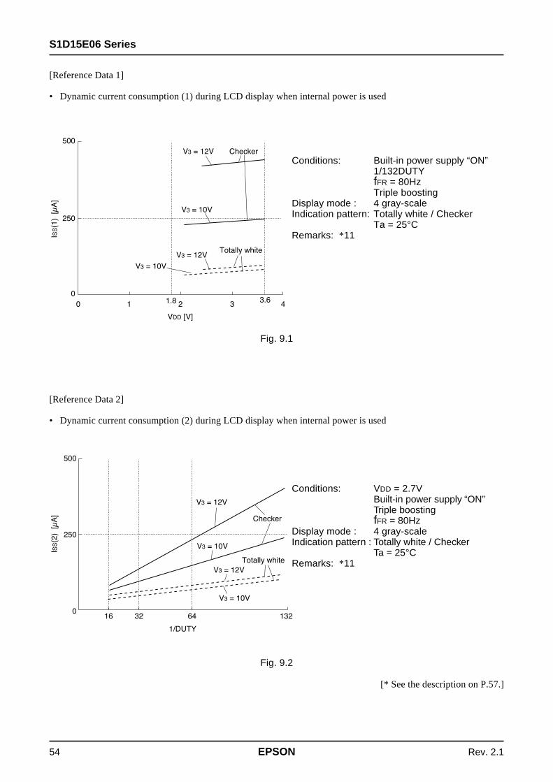
S1D15E06 Series
54 EPSON Rev. 2.1
[Reference Data 2]
• Dynamic current consumption (2) during LCD display when internal power is used
Conditions: VDD = 2.7VBuilt-in power supply “ON”Triple boostingfFR = 80Hz
Display mode : 4 gray-scaleIndication pattern : Totally white / Checker
Ta = 25°CRemarks: *11
500
250
016 32 64 132
1/DUTY
ISS(2)[µA]
Checker
V3 = 12V
V3 = 10V
V3 = 10V
V3 = 12V
Totally white
Fig. 9.2
[* See the description on P.57.]
[Reference Data 1]
Conditions: Built-in power supply “ON”1/132DUTYfFR = 80HzTriple boosting
Display mode : 4 gray-scaleIndication pattern: Totally white / Checker
Ta = 25°CRemarks: *11
• Dynamic current consumption (1) during LCD display when internal power is used
Fig. 9.1
500
250
0
0 1 2 3 43.61.8
VDD [V]
ISS(1)[µA]
CheckerV3 = 12V
V3 = 10V
V3 = 12V
V3 = 10V
Totally white

S1D15E06 Series
Rev. 2.1 EPSON 55
[Reference Data 3]
• Dynamic current consumption (3) during access
Indicates the current consumption when the checkerpattern is always written by fCYC. When notaccessed, only ISS(1) remains.
Conditions: Built-in voltage usedTriple boostingV3= 12.0V, VDD = 2.7VTa = 25°CfFR=80Hz 1/132 Duty
10
1
0.1
0.010.001 0.01 0.1 1 10
ISS(3
) [m
A]
fCYC [MHz]
Fig. 9.3

S1D15E06 Series
56 EPSON Rev. 2.1
[Reference Data 4]
Remarks: *2
• Operating voltage range (S1D15E06D01****)
Remarks: *2
16.0
14.0
00 1 2 3 4
VDD [V]
3.4
1.7 3.6
V3
[V]
Operating range
14.0
10.5
7.0
3.5
00 1 2 3 4
VDD [V]
3.4
1.7 3.6
V3
[V]
Operating range
Fig. 9.4.1
• Operating voltage range (S1D15E06D03****)
Fig. 9.4.2
[* See the description on P.57.]

S1D15E06 Series
Rev. 2.1 EPSON 57
(fFR indicates the cycle of rewriting one screen; it does not indicate FR signal cycle.)
[Asterisked references]*1. Does not guarantee if there is an abrupt voltage variation during MPU access.*2. For VDD and V3 system operating voltage range, see Fig. 9.5.
Applicable when the external power supply is used.*3. A0, D0 to D5, D6(SCL), D7(SI), RD(E), WR(R/W), CS1, CS2, CLS, CL, FR, F1, F2, CA, M/S, C86, P/S, DOF,
RES and TEST pins*4. D0 to D7, FR, DOF, CL, F1, F2 and CA pins*5. A0, RD(E), WR(R/W), CS1, CS2, CLS, M/S, C86, P/S, RES and TEST pins*6. Applicable when D0 to D5, D6(SCL), D7(S1), CL, FR, DOF, F1, F2 and CA pins have a high impedance.*7. Indicates the resistance when 0.1V voltage is applied between the output pin SEGn or COMn and each power
supply (V2, V1, VC, MV1, MV2).RON =0.1V/∆I (where ∆I denotes current when 0.1V is applied when power is on).
*8. For the relationship between oscillation frequency and frame frequency, see Table 9.8. The standard values ofthe external input item are recommended ones.
*9. The VC voltage regulating circuit should be adjusted within the electronic volume operation range.*10. Indicates the current consumed by a single IC when display is on. Use the electronic volume for voltage
regulation. Also use the internal oscillator circuit. The current due to LCD panel capacity and wiring capacityis not included. Applicable when there is access from the MPU.
• Relationship between oscillation frequency fOSC, display clock frequency fCL and liquid crystal frame fFR
Table 9.8
Item fCL Display mode fFR
Built-in oscillator See p. 24 Binary display (fCL × DUTY)/4circuit used 4 gray-scale (fCL × DUTY)/8
Built-in oscillator circuit External input (fCL) Binary display (fCL × DUTY)/4not used 4 gray-scale (fCL × DUTY)/8

S1D15E06 Series
58 EPSON Rev. 2.1
10. TIMING CHARACTERISTICS(1) System path read/write characteristics 1 (80 system MPU)
Fig. 10.1
Table 10.1.1
A0
CS1(CS2=“1”)
WR, RD
tACC8 tOH8
tDS8
tf tr
tCYC8
tAH8tAW8
tCCLR, tCCLW
tCCHR, tCCHW
tDH8
CS1(CS2=“1”)
WR, RD
*1
*2
D0 to D7(Write)
D0 to D7(Read)
Parameter Signal Symbol ConditionSpecified value
UnitMin. Max.
Address hold time A0 tAH8 0 — nsAddress setup time tAW8 0 —
System write cycle time WR tWCYC8 200 —System read cycle time RD tRCYC8 300 —
Control LOW-pulse width (Write) WR tCCLW 60 —Control LOW-pulse width (Read) RD tCCLR 100 —Control HIGH-pulse width (Write) WR tCCHW 60 —Control HIGH-pulse width (Read) RD tCCHR 100 —
Data setup time D0 to D7 tDS8 20 —Data hold time tDH8 10 —
RD access time tACC8 CL=100pF — 80Output disable time tOH8 10 80
[VDD = 3.0V to 3.6V, Ta = –40 to +85°C]

S1D15E06 Series
Rev. 2.1 EPSON 59
Table 10.1.2
Table 10.1.3
Parameter Signal Symbol ConditionSpecified value
UnitMin. Max.
Address hold time A0 tAH8 0 — nsAddress setup time tAW8 0 —
System write cycle time WR tWCYC8 400 —System read cycle time RD tRCYC8 600 —
Control LOW-pulse width (Write) WR tCCLW 100 —Control LOW-pulse width (Read) RD tCCLR 250 —Control HIGH-pulse width (Write) WR tCCHW 140 —Control HIGH-pulse width (Read) RD tCCHR 250 —
Data setup time D0 to D7 tDS8 40 —Data hold time tDH8 20 —
RD access time tACC8 CL=100pF — 200Output disable time tOH8 10 200
[VDD = 1.7V to 2.4V, Ta = –40 to +85°C]
Parameter Signal Symbol ConditionSpecified value
UnitMin. Max.
Address hold time A0 tAH8 0 — nsAddress setup time tAW8 0 —
System write cycle time WR tWCYC8 300 —System read cycle time RD tRCYC8 400 —
Control LOW-pulse width (Write) WR tCCLW 80 —Control LOW-pulse width (Read) RD tCCLR 200 —Control HIGH-pulse width (Write) WR tCCHW 80 —Control HIGH-pulse width (Read) RD tCCHR 200 —
Data setup time D0 to D7 tDS8 30 —Data hold time tDH8 15 —
RD access time tACC8 CL=100pF — 120Output disable time tOH8 10 120
[VDD = 2.4V to 3.0V, Ta = –40 to +85°C]
*1. This is in case of making the access by WR and RD, setting the CS1 = LOW.*2. This is in case of making the access by CS1, setting the WR, RD = LOW.*3. Input signal rise and fall time (tr, tf) must not exceed 15 ns. When the system cycle time is used at a high speed,
it is specified by (tr + tf) ≤ (tCYC8 – tCCLW – tCCHW) or (tr + tf) ≤ (tCYC8 – tCCLR – tCCHR).*4. Timing is entirely specified with reference to 20% or 80% of VDD.*5. tCCLW and tCCLR are specified in terms of the overlapped period when CS1 is at LOW (CS2 = HIGH) level and
WR and RD are at LOW level.

S1D15E06 Series
60 EPSON Rev. 2.1
(2) System path read/write characteristics 2 (68 system MPU)
Fig. 10.2
Table 10.2.1
[VDD = 3.0V to 3.6V, Ta = –40 to +85°C]
A0R/W
CS1(CS2=“1”)
E
D0 to D7(Write)
D0 to D7(Read)
tACC6 tOH6
tDS6
tCYC6
tAH6tAW6
tEWHR, tEWHW
tf tr
tEWLR, tEWLW
tDH6
CS1(CS2=“1”)
E
*1
*2
Parameter Signal Symbol ConditionSpecified value
UnitMin. Max.
Address hold time A0 tAH6 0 — nsAddress setup time tAW6 0 —
System write cycle time E tWCYC6 200 —System read cycle time tRCYC6 300 —
Data setup time D0 to D7 tDS6 20 —Data hold time tDH6 10 —
Access time tACC6 CL=100pF — 80Output disable time tOH6 10 80
Enable HIGH-pulse width Read E tEWHR 100 —Write tEWHW 60 —
Enable LOW-pulse width Read E tEWLR 100 —Write tEWLW 60 —

S1D15E06 Series
Rev. 2.1 EPSON 61
Parameter Signal Symbol ConditionSpecified value
UnitMin. Max.
Address hold time A0 tAH6 0 — nsAddress setup time tAW6 0 —
System write cycle time E tWCYC6 300 —System read cycle time tRCYC6 400 —
Data setup time D0 to D7 tDS6 30 —Data hold time tDH6 15 —
Access time tACC6 CL=100pF — 120Output disable time tOH6 10 120
Enable HIGH-pulse width Read E tEWHR 150 —Write tEWHW 80 —
Enable LOW-pulse width Read E tEWLR 150 —Write tEWLW 80 —
Table 10.2.2[VDD = 2.4V to 3.0V, Ta = –40 to +85°C]
Table 10.2.3
Parameter Signal Symbol ConditionSpecified value
UnitMin. Max.
Address hold time A0 tAH6 0 — nsAddress setup time tAW6 0 —
System write cycle time E tWCYC6 400 —System read cycle time tRCYC6 600 —
Data setup time D0 to D7 tDS6 40 —Data hold time tDH6 20 —
Access time tACC6 CL=100pF — 200Output disable time tOH6 10 200
Enable HIGH-pulse width Read E tEWHR 250 —Write tEWHW 100 —
Enable LOW-pulse width Read E tEWLR 250 —Write tEWLW 140 —
[VDD = 1.7V to 2.4V, Ta = –40 to +85°C]
*1 This is in case of making the access by E, setting the CS1 = LOW.*2 This is in case of making the access by CS1, setting the E = HIGH.*3 The rise time and the fall time (tr & tf) of the input signals should be set to 15ns or less. When it is necessary to
use the system cycle time at high speed, the rise time and the fall time should be so set to conformto (tr+tf) ≤ (tCVC6-tEWLW-tEWHW) or (tr+tf) ≤ (tCYC6-tEWLR-tEWHR).
*4 All the timing should basically be set to 20% and 80% of the “VDD”.*5 tEWLW, tEWLR should be set to the overlapping zone where the CS1 is on the LOW level (CS2 = HIGH level) and
where the E is on the HIGH level.
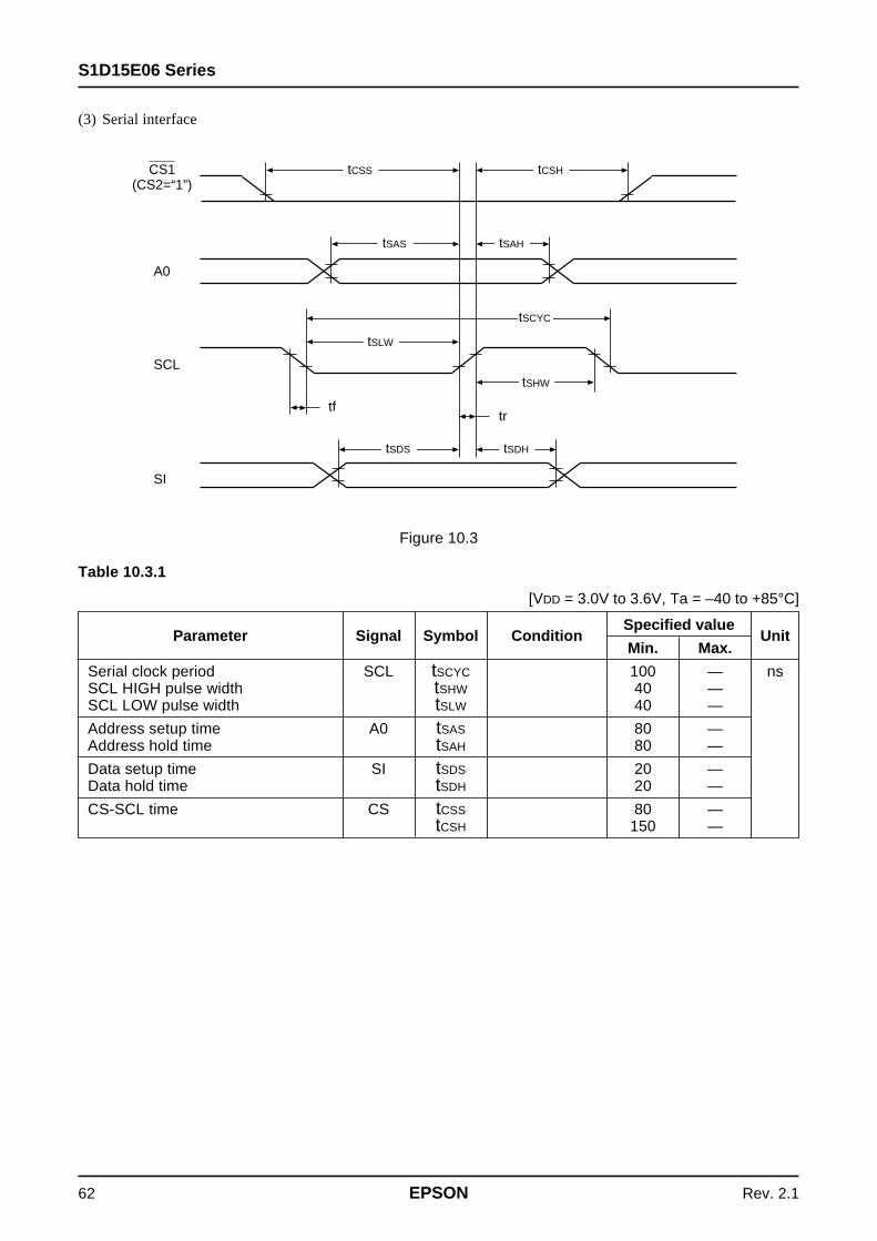
S1D15E06 Series
62 EPSON Rev. 2.1
Parameter Signal Symbol ConditionSpecified value
UnitMin. Max.
Serial clock period SCL tSCYC 100 — nsSCL HIGH pulse width tSHW 40 —SCL LOW pulse width tSLW 40 —
Address setup time A0 tSAS 80 —Address hold time tSAH 80 —
Data setup time SI tSDS 20 —Data hold time tSDH 20 —
CS-SCL time CS tCSS 80 —tCSH 150 —
[VDD = 3.0V to 3.6V, Ta = –40 to +85°C]
CS1(CS2=“1”)
A0
SCL
SI
tCSS
tSAS tSAH
tSCYC
tSLW
tSHW
trtf
tSDS tSDH
tCSH
(3) Serial interface
Figure 10.3
Table 10.3.1

S1D15E06 Series
Rev. 2.1 EPSON 63
Parameter Signal Symbol ConditionSpecified value
UnitMin. Max.
Serial clock period SCL tSCYC 125 — nsSCL HIGH pulse width tSHW 50 —SCL LOW pulse width tSLW 50 —
Address setup time A0 tSAS 100 —Address hold time tSAH 100 —
Data setup time SI tSDS 30 —Data hold time tSDH 30 —
CS-SCL time CS tCSS 100 —tCSH 200 —
[VDD = 2.4V to 3.0V, Ta = –40 to +85°C]
Parameter Signal Symbol ConditionSpecified value
UnitMin. Max.
Serial clock period SCL tSCYC 154 — nsSCL HIGH pulse width tSHW 60 —SCL LOW pulse width tSLW 60 —
Address setup time A0 tSAS 120 —Address hold time tSAH 140 —
Data setup time SI tSDS 40 —Data hold time tSDH 40 —
CS-SCL time CS tCSS 120 —tCSH 350 —
[VDD = 1.7V to 2.4V, Ta = –40 to +85°C]
*1. Input signal rise and fall time (tr, tf) must not exceed 15 ns.*2. Timing is entirely specified with reference to 20% or 80% of VDD.
Table 10.3.2
Table 10.3.3

S1D15E06 Series
64 EPSON Rev. 2.1
CL(OUT)
FR
F1, F2
CA
tDFR
tDF1,F2
tDCA
Parameter Signal Symbol ConditionSpecified value
UnitMin. Typ. Max.
FR delay time FR tDFR CL = 50pF — 125 312 nsF1, F2 delay time F1, F2 tDF1, tF2 — 125 312 nsCA delay time CA tDCA — 125 312 ns
[VDD = 3.0V to 3.6V, Ta = –40 to +85°C]
Parameter Signal Symbol ConditionSpecified value
UnitMin. Typ. Max.
FR delay time FR tDFR CL = 50pF — 150 360 nsF1, F2 delay time F1, F2 tDF1, tF2 — 150 360 nsCA delay time CA tDCA — 150 360 ns
[VDD = 2.4V to 3.0V, Ta = –40 to +85°C]
Parameter Signal Symbol ConditionSpecified value
UnitMin. Typ. Max.
FR delay time FR tDFR CL = 50pF — 225 514 nsF1, F2 delay time F1, F2 tDF1, tF2 — 225 514 nsCA delay time CA tDCA — 225 514 ns
[VDD = 1.7V to 2.4V, Ta = –40 to +85°C]
(4) Display control output timing
Fig. 10.4
Table 10.4.1
Table 10.4.2
Table 10.4.3
*1. Valid only in master operation*2. Timing is entirely specified with reference to 20% or 80% of VDD.

S1D15E06 Series
Rev. 2.1 EPSON 65
tRW
tR
End of resettingDuring resetting
RES
Internal state
Parameter Signal Symbol ConditionSpecified value
UnitMin. Typ. Max.
Reset time tR — — 0.5 µs
Reset LOW pulse width RES tRW 0.5 — —
[VDD = 3.0V to 3.6V, Ta = –40 to +85°C]
Parameter Signal Symbol ConditionSpecified value
UnitMin. Typ. Max.
Reset time tR — — 1.0 µs
Reset LOW pulse width RES tRW 1.0 — —
[VDD = 2.4V to 3.0V, Ta = –40 to +85°C]
Parameter Signal Symbol ConditionSpecified value
UnitMin. Typ. Max.
Reset time tR — — 1.5 µs
Reset LOW pulse width RES tRW 1.5 — —
[VDD = 1.7V to 2.4V, Ta = –40 to +85°C]
*1. Timing is entirely specified with reference to 20% or 80% of VDD.
(5) Reset input timing
Fig. 10.5
Table 10.5.1
Table 10.5.2
Table 10.5.3

S1D15E06 Series
66 EPSON Rev. 2.1
VDDVCC
GND
Decoder
RESET
MP
U
A0
D0 to D7RDWRRES
CS1CS2
A0
D0 to D7RDWR
RES
A1 to A7IORQ
VDD
C86
P/SVSS
VSS
S1D
15E
06 S
erie
s
VDDVCC
GND
Decoder
RESET
MP
U
A0
D0 to D7ER/WRES
CS1CS2
A0
D0 to D7E
R/WRES
A1 to A15VMA
VDD
C86
P/SVSS
VSS
S1D
15E
06 S
erie
s
VDDVCC
GND
Decoder
RESET
MP
U
A0
SISCLRES
CS1CS2
A0
Port 1Port 2
RES
A1 to A7
VDD or VSSC86
P/SVSS
VSS
VDD
S1D
15E
06 S
erie
s
11. MPU INTERFACE (Reference Example)The S1D15E06 series can be connected to the 80 series MPU and 68 series MPU. Use of a serial interface allowsoperation with a smaller number of signal lines.You can expand the display area using the S1D15E06 series as a multi-chip. In this case, the IC to be accesses can beselected individually by the chip select signal. After initialization by the RES pin, each input terminal of the S1D15E06series must be placed under normal control.
(1) 80 series MPU
Fig. 11.1(2) 68 series MPU
Fig. 11.2(3) Serial interface
Fig. 11.3

S1D15E06 Series
Rev. 2.1 EPSON 67
CLFR
DOFF1F2CA
M/S
S1D15E06 (Master) S1D15E06 (Slave)
VDD
VDDVSS
CLS CLS
M/S
V3
V2
V1
VC
MV1
MV2
(VSS) MV3
CLFRDOFF1F2CA
V3
V2
V1
VC
MV1
MV2
MV3 (VSS)
12. CONNECTION BETWEEN LCD DRIVERS (Reference example)You can easily expand the liquid crystal display area using the S1D15E06 series as a multi-chip. In this case, use thesame model as the master and slave systems.
Fig. 12 Master/slave connection example (S1D15E06)

S1D15E06 Series
68 EPSON Rev. 2.1
13. LCD PANEL WIRING (Reference example)You can easily expand the liquid crystal display area using the S1D15E06 series as a multi-chip. In the case of multi-chip configuration, use the same models.
(1) Single chip configuration example
Fig. 13.1 Single chip configuration example (S1D15E06)
(2) Double chip configuration example
Fig. 13.2 Double chip configuration example (S1D15E06)
160 x 132 Dots
COM SEG COM
S1D15E06Master
320 x 132 Dots
COM COMSEG SEG
S1D15E06Master
S1D15E06Slave
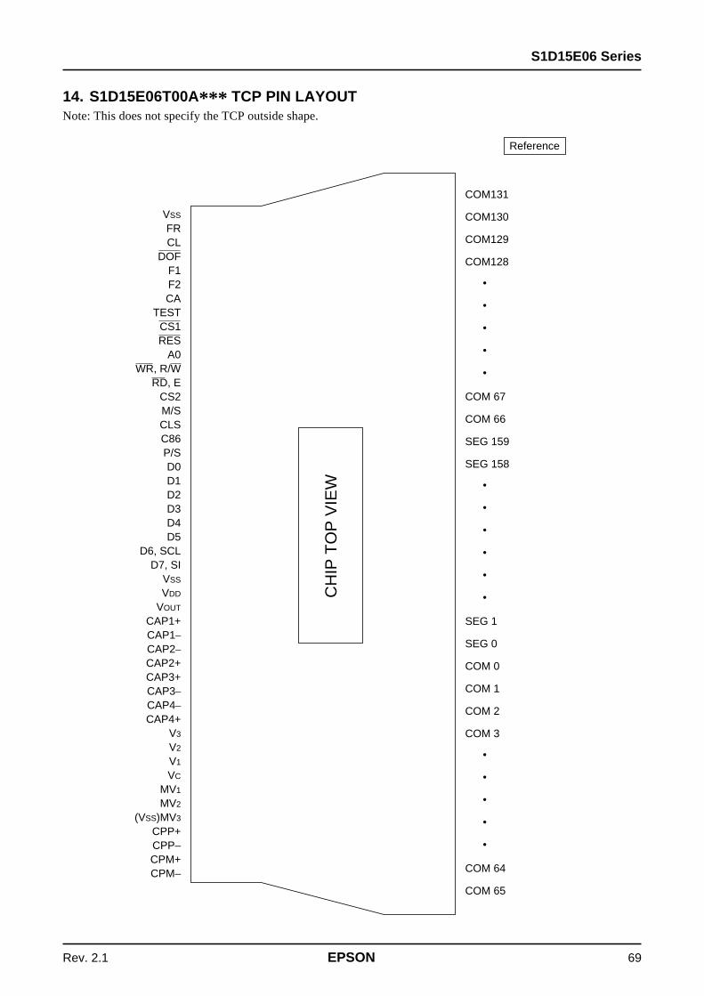
S1D15E06 Series
Rev. 2.1 EPSON 69
14. S1D15E06T00A*** TCP PIN LAYOUTNote: This does not specify the TCP outside shape.
VSS
FRCL
DOFF1F2CA
TESTCS1RES
A0WR, R/W
RD, ECS2M/SCLSC86P/SD0D1D2D3D4D5
D6, SCLD7, SI
VSS
VDD
VOUT
CAP1+CAP1–CAP2–CAP2+CAP3+CAP3–CAP4–CAP4+
V3
V2
V1
VC
MV1
MV2
(VSS)MV3
CPP+CPP–CPM+CPM–
COM131
COM130
COM129
COM128
COM 67
COM 66
SEG 159
SEG 158
SEG 1
SEG 0
COM 0
COM 1
COM 2
COM 3
COM 64
COM 65
•
•
•
•
•
•
•
•
•
•
•
•
•
•
•
•
CH
IP T
OP
VIE
W
Reference

S1D15E06 Series
70 EPSON Rev. 2.1
15. TCP DIMENSIONS (Reference example)

S1D15E06 Series
Rev. 2.1 EPSON 71
16. CAUTIONSCautions must be exercised on the following points when using this Development Specification:1. This Development Specification is subject to change for engineering improvement.2. This Development Specification does not guarantee execution of the industrial proprietary rights or other rights, or
grant a license. Examples of applications described in This Development Specification are intended for yourunderstanding of the Product. We are not responsible for any circuit problem or the like arising from the use of them.
3. Reproduction or copy of any part or whole of this Development Specification without permission of our company,or use thereof for other business purposes is strictly prohibited.
For the use of the semi-conductor,cautions must be exercised on the following points:
[Cautions against Light]The semiconductor will be subject to changes in characteristics when light is applied. If this IC is exposed to light,operation error may occur. To protect the IC against light, the following points should be noted regarding the substrateor product where this IC is mounted:(1) Designing and mounting must be provided to get a structure which ensures a sufficient resistance of the IC to
light in practical use.(2) In the inspection process, environmental configuration must be provided to ensure a sufficient resistance of the
IC to light.(3) Means must be taken to ensure resistance to light on all the surfaces, backs and sides of the IC