s1d13506f00a data sheet - epson · s1d13506f00a color lcd/crt/tv controller ... - edo-dram up to...
TRANSCRIPT

1
PF977-04
S1D13506F00AColor LCD/CRT/TV Controller
DESCRIPTIONThe S1D13506 is a color LCD/CRT/TV graphics controller interfacing to a wide range of CPUs and displaydevices. The S1D13506 architecture is designed to meet the low cost, low power requirements of theembedded markets, such as Mobile Communications, Hand-Held PC’s, and Office Automation.
The S1D13506 supports multiple CPUs, all LCD panel types, CRT, TV, and additionally provides a number ofdifferentiating features. Products requiring digital camera input can take advantage of the directly supportedWINNOV VideumCam™ digital interface. The EPSON Independent Simultaneous Display (EISD) capabilityallows the user to configure two different images on two different displays, while the SviwelView™, HardwareCursor, Ink Layer, and BitBLT engine offer substantial performance benefits. These features, combined withthe S1D13506’s Operating System independence, make it an ideal display solution for a wide variety ofapplications.
FEATURES
Memory Interface• 16-bit DRAM interface:
- EDO-DRAM up to 40MHz data rate(80M Bytes/s).
- FPM-DRAM up to 25MHz data rate(50M Bytes/s).
• Memory size options:- 512K bytes using one 256Kx16 device.- 2M bytes using one 1Mx16 device.
• A configuration register can be programmed toenhance performance by tailoring the memorycontrol output timing to the DRAM device.
• The complete 2M byte display buffer addressspace is directly and contiguously availablethrough the 21-bit address bus.
CPU Interface• Supports the following interfaces:
- Epson S1C33 (16-bit interface to 32-bitmicroprocessor).
- Hitachi SH-4 bus interface.- Hitachi SH-3 bus interface.- MIPS/ISA.- Motorola MC68000 (16-bit interface to 16/32-bit
microprocessor/microcontroller).- Motorola MC68030 (16-bit interface to 16/32-bit
microprocessor/microcontroller).- Motorola PowerPC MPC82x (16-bit interface to
32-bit microprocessor).- MPU bus interface with programmable READY.- NEC MIPS VR41xx.
- PC Card (PCMCIA).- Philips MIPS PR31500/31700.- Toshiba MIPS TX39xx.- StrongARM (PC Card).
• One-stage write buffer for minimum wait-stateCPU writes.
• Registers are memory-mapped – the M/R# pinselects between display buffer and registeraddress space.
Display Support• 4/8-bit monochrome or 4/8/16-bit color LCD
interface for single-panel, single-drive displays.• 8-bit monochrome or 8/16-bit color LCD interface
for dual-panel, dual-drive displays.• Direct support for 9/12-bit TFT/D-TFD, 18-bit TFT/
D-TFD is supported up to 64K colors.• Direct support for CRT up to 64K colors using
Embedded RAMDAC.• Direct support for NTSC/PAL TV output using
Embedded RAMDAC.
Display Modes• 4/8/15/16 bit-per-pixel (bpp) color depths.• Up to 64 shades of gray on monochrome passive
LCD panels using Frame Rate Modulation (FRM)and Dithering.
• Up to 32K/64K colors in 15/16 bpp modes on colorpassive LCD panels using dithering.
• Up to 64K colors on TFT/D-TFD, CRT and TV.• 4/8 bit-per-pixel color depths are mapped using
three 256x4 Look-Up Tables (LUT) allowing 16/256 out of a possible 4096 colors.
• Separate LUTs for LCD and CRT/TV.

2
S1D13506F00A
• 15/16 bit-per-pixel color depths are mappeddirectly, bypassing the LUT.
• Example Resolutions: 320 x 240 at a color depth of 16 bpp. 640 x 240 at a color depth of 16 bpp. 640 x 480 at a color depth of 16 bpp. 800 x 600 at a color depth of 16 bpp.
Display Features• SwivelView™: 90°, 180°, 270° hardware rotation
of display image.• EPSON Independent Simultaneous Display
(EISD): displays independent images on differentdisplays (CRT or TV and passive or TFT/D-TFDpanel).
• Virtual Display Support: displays images largerthan the panel size through the use of panningand scrolling.
• Hardware Cursor/Ink Layer: separate 64x64x2hardware cursor or 2-bit ink layer for both LCDand CRT/TV.
• Double Buffering/Multi-pages: for smoothanimation and instantaneous screen update.
Clock Source• Memory clock can be derived from CLKI or
BUSCLK pin. It can be internally divided by 2.• Pixel clock can be derived from CLKI, CLKI2, or
BUSCLK pin. It can be internally divided by 2, 3 or4.
• Bus clock can be BUSCLK or (BUSCLK)/2, i.e. a2x clock may be used.
Acceleration• 2D Engine including the following 2 ROP BitBlts:
- Write BLT.- Move BLT.- Solid Fill.- Pattern Fill.- Transparent Write BLT.- Transparent Move BLT.- Read BLT.- Color Expansion.- Move BLT with Color Expansion.
MediaPlug Interface• Built-in WINNOV MediaPlug interface.• VideumCam support at resolution of 320x240x256
color at 30fps.
Miscellaneous• The memory data bus, MD[15:0], is used to
configure the chip at power-on.• Three General Purpose Input/Output pins,
GPIO[3:1], are available if upper Memory Addresspins are not required for asymmetric DRAMsupport.
• Power save mode is initiated by software.• Operating voltage from 2.7 volts to 5.5 volts.• 128-pin QFP15 surface mount package.
3
S1D13506F00A
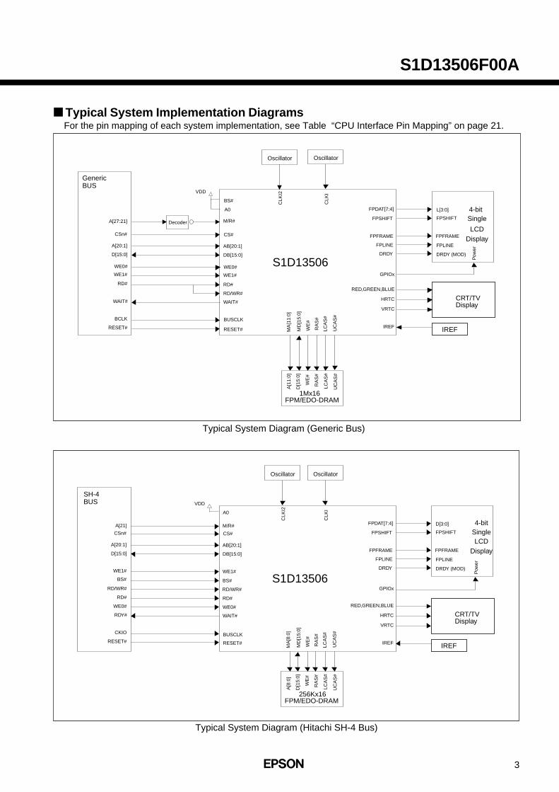
Typical System Implementation DiagramsFor the pin mapping of each system implementation, see Table “CPU Interface Pin Mapping” on page 21.
S1D13506
FPFRAME
FPSHIFT
FPLINE
DRDY
FPDAT[7:4]
CLK
I
Oscillator
FPFRAME
FPSHIFT
FPLINE
DRDY (MOD)
D[3:0] 4-bit
LCDDisplay
SH-4BUS
RESET#
WE0#
D[15:0]
BS#
RD/WR#
RD#
RDY#
A[20:1]
CKIO
WE0#
RD/WR#
AB[20:1]
DB[15:0]
WE1#
BS#
RD#
M/R#
CS#
BUSCLK
WAIT#
RESET#
A[21]
CSn#
WE1#
GPIOx
LCA
S#
UC
AS
#
MA
[8:0
]
MD
[15:
0]
WE
#
RA
S#
RED,GREEN,BLUE
HRTC
VRTC
CRT/TVDisplay
IREF IREF
WE
#
A[8
:0]
D[1
5:0]
RA
S#
256Kx16
LCA
S#
UC
AS
#
FPM/EDO-DRAM
CLK
I2
Oscillator
Single
Pow
er
A0
VDD
Typical System Diagram (Generic Bus)
S1D13506
FPFRAME
FPSHIFT
FPLINE
DRDY
FPDAT[7:4]
CLK
I
Oscillator
FPFRAME
FPSHIFT
FPLINE
DRDY (MOD)
L[3:0]
Single
LCDDisplay
GenericBUS
GPIOx
WE
#
A[1
1:0]
D[1
5:0]
RA
S#
1Mx16
LCA
S#
UC
AS
#
MA
[11:
0]
MD
[15:
0]
WE
#
RA
S#
LCA
S#
UC
AS
#
FPM/EDO-DRAM
RED,GREEN,BLUE
HRTC
VRTC
CRT/TVDisplay
IREF IREF
CLK
I2
Oscillator
4-bit
Pow
er
RESET#
D[15:0]
RD#
WAIT#
A[20:1]
BCLK
RD/WR#
AB[20:1]
DB[15:0]
WE1#
RD#
M/R#
CS#
BUSCLK
WAIT#
RESET#
A[27:21]
CSn#
WE1#
Decoder
WE0#WE0#
BS#
VDD
A0
Typical System Diagram (Hitachi SH-4 Bus)
4
S1D13506F00A
S1D13506
FPFRAME
FPSHIFT
FPLINE
DRDY
FPDAT[7:0]
CLK
I
Oscillator
FPFRAME
FPSHIFT
FPLINE
DRDY (MOD)
D[7:0]
Single
LCDDisplay
SH-3BUS
RESET#
WE0#
D[15:0]
BS#
RD/WR#
RD#
WAIT#
A[20:1]
CKIO
WE0#
RD/WR#
AB[20:1]
DB[15:0]
WE1#
BS#
RD#
M/R#
CS#
BUSCLK
WAIT#
RESET#
A[21]
CSn#
WE1#
GPIOx
LCA
S#
UC
AS
#
MA
[8:0
]
MD
[15:
0]
WE
#
RA
S#
RED,GREEN,BLUE
HRTC
VRTC
CRT/TVDisplay
IREF IREF
WE
#
A[8
:0]
D[1
5:0]
RA
S#
256Kx16
LCA
S#
UC
AS
#
FPM/EDO-DRAM
CLK
I2
Oscillator
8-bit
Pow
er
A0
VDD
S1D13506
FPFRAME
FPSHIFT
FPLINE
DRDY
FPDAT[7:4]
FPDAT[3:0]
CLK
I
Oscillator
FPFRAME
FPSHIFT
FPLINE
DRDY (MOD)
UD[3:0]
LD[3:0]
Dual
LCDDisplay
MC68000BUS
RESET#
LDS#
D[15:0]
AS#
R/W#
DTACK#
A[20:0]
CLK
AB0
RD/WR#
AB[20:0]
DB[15:0]
WE1#
BS#
M/R#
CS#
BUSCLK
WAIT#
RESET#
A[23:21]FC0, FC1 Decoder
Decoder
UDS# GPIOx
LCA
S#
UC
AS
#
MA
[11:
0]
MD
[15:
0]
WE
#
RA
S#
RED,GREEN,BLUE
HRTC
VRTC
CRT/TVDisplay
IREF IREF
WE
#
A[1
1:0]
D[1
5:0]
RA
S#
256Kx16
LCA
S#
UC
AS
#
FPM/EDO-DRAM
CLK
I2
Oscillator
8-bit
Pow
er
RD#WE0#
VDD
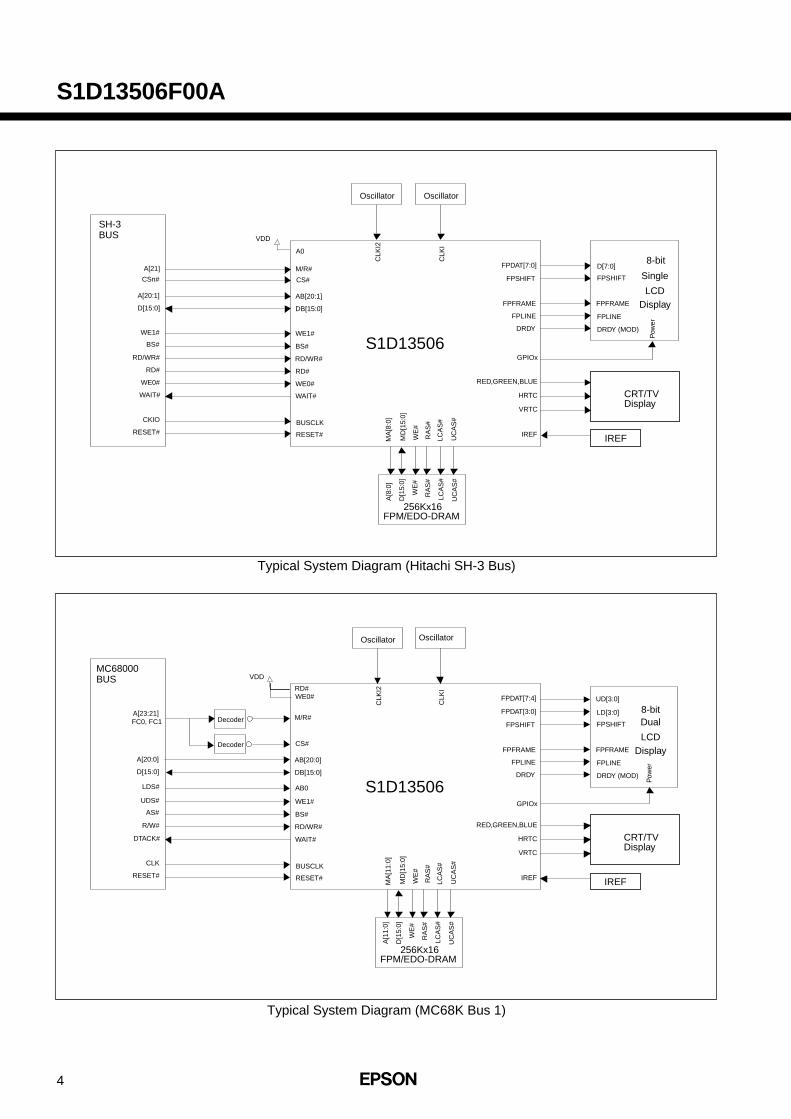
Typical System Diagram (Hitachi SH-3 Bus)
Typical System Diagram (MC68K Bus 1)

5
S1D13506F00A
S1D13506
FPFRAME
FPSHIFT
FPLINE
DRDY
FPDAT[8:0]
CLK
I
Oscillator
FPFRAME
FPSHIFT
FPLINE
DRDY (MOD)
D[8:0]
9-bit
TFTDisplay
MC68030BUS
RESET#
SIZ0
D[31:16]
AS#
R/W#
SIZ1
DSACK1#
A[20:0]
CLK
WE0#
RD/WR#
AB[20:0]
DB[15:0]
WE1#
BS#
RD#
M/R#
CS#
BUSCLK
WAIT#
RESET#
A[31:21]FC0, FC1 Decoder
Decoder
DS#
GPIOx
WE
#
A[8
:0]
D[1
5:0]
RA
S#
256Kx16
LCA
S#
UC
AS
#
MA
[8:0
]
MD
[15:
0]
WE
#
RA
S#
LCA
S#
UC
AS
#
FPM/EDO-DRAM
RED,GREEN,BLUE
HRTC
VRTC
CRT/TVDisplay
IREF IREF
CLK
I2
Oscillator
Pow
er
Typical System Diagram (Motorola PowerPC Bus)
Typical System Diagram (MC68K Bus 2, Motorola 32-Bit 68030)
S1D13506
FPFRAME
FPSHIFT
FPLINE
DRDY
FPDAT[15:0]
CLK
I
Oscillator
FPFRAME
FPSHIFT
FPLINE
DRDY (MOD)
D[15:0]
Single
LCDDisplay
PowerPCBUS
RESET#
TSIZ1
D[0:15]
TS#
RD/WR#
TSIZ0
TA#
A[11:31]
CLKOUT
WE0#
RD/WR#
AB[20:0]
DB[15:0]
WE1#
BS#
RD#
M/R#
CS#
BUSCLK
WAIT#
RESET#
A[0:10]Decoder
Decoder
BI#
GPIOx
WE
#
A[8
:0]
D[1
5:0]
RA
S#
256Kx16
LCA
S#
UC
AS
#
MA
[8:0
]
MD
[15:
0]
WE
#
RA
S#
LCA
S#
UC
AS
#
FPM/EDO-DRAM
RED,GREEN,BLUE
HRTC
VRTC
CRT/TVDisplay
IREF IREF
CLK
I2
Oscillator
16-bit
Pow
er
6
S1D13506F00A
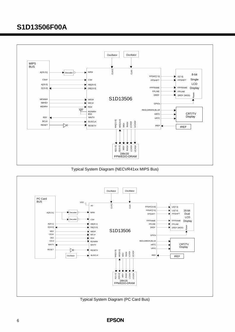
Typical System Diagram (NECVR41xx MIPS Bus)
S1D13506
FPFRAME
FPSHIFT
FPLINE
DRDY
FPDAT[7:0]
CLK
I
Oscillator
FPFRAME
FPSHIFT
FPLINE
DRDY (MOD)
D[7:0]
Single
LCDDisplay
MIPSBUS
RESET
D[15:0]
MEMR#
RDY
A[20:0]
BCLK
RD/WR#
AB[20:0]
DB[15:0]
WE1#
RD#
M/R#
CS#
BUSCLK
WAIT#
RESET#
A[25:21]
CSn#
SBHE# GPIOx
WE
#
A[1
1:0]
D[1
5:0]
RA
S#
1Mx16
LCA
S#
UC
AS
#
MA
[11:
0]
MD
[15:
0]
WE
#
RA
S#
LCA
S#
UC
AS
#
FPM/EDO-DRAM
Decoder
WE0#MEMW#
RED,GREEN,BLUE
HRTC
VRTC
CRT/TVDisplay
IREF IREF
VDDC
LKI2
Oscillator
8-bit
Pow
er
BS#
Typical System Diagram (PC Card Bus)
S1D13506
FPFRAME
FPSHIFT
FPLINE
DRDY
FPDAT[15:8]
FPDAT[7:0]
CLK
I
Oscillator
FPFRAME
FPSHIFT
FPLINE
DRDY (MOD)
UD[7:0]
LD[7:0]
DualLCD
Display
PC CardBUS
RESET
D[15:0]
OE#
WAIT#
A[20:1]
RD/WR#
AB[20:1]
DB[15:0]
WE1#
RD#
M/R#
CS#
BUSCLK
WAIT#
RESET#
A[25:21]
CE2# GPIOx
WE
#
A[1
1:0]
D[1
5:0]
RA
S#
1Mx16
LCA
S#
UC
AS
#
MA
[11:
0]
MD
[15:
0]
WE
#
RA
S#
LCA
S#
UC
AS
#
FPM/EDO-DRAM
WE0#WE#
RED,GREEN,BLUE
HRTC
VRTC
CRT/TVDisplay
IREF IREF
Decoder
Decoder
CE1#
CLK
I2
Oscillator
16-bit
Pow
er
A0
VDD
Oscillator

7
S1D13506F00A
Typical System Diagram (Toshiba MIPS TX3912 Bus)
Typical System Diagram (Philips MIPS PR31500/PR31700 Bus)
S1D13506
FPFRAME
FPSHIFT
FPLINE
DRDY
FPDAT[7:4]
FPDAT[3:0]
CLK
I
Oscillator
FPFRAME
FPSHIFT
FPLINE
DRDY (MOD)
UD[3:0]
LD[3:0]
Dual
LCDDisplay
GPIOx
WE
#
A[1
1:0]
D[1
5:0]
RA
S#
1Mx16
LCA
S#
UC
AS
#
MA
[11:
0]
MD
[15:
0]
WE
#
RA
S#
LCA
S#
UC
AS
#
FPM/EDO-DRAM
RED,GREEN,BLUE
HRTC
VRTC
CRT/TVDisplay
IREF IREF
PR31500
BUS
RESET#
/WE
D[31:24]
/CARDxCSL
/RD
/CARDxWAIT
A[12:0]
DCLKOUT
WE0#
RD/WR#
AB[12:0]
DB[15:8]
WE1#
BS#
RD#
M/R#CS#
BUSCLK
WAIT#
RESET#
/CARDxCSH
AB[16:13]
ALE/CARDREG
/CARDIORD
AB20
AB19
AB18
AB17/CARDIOWR
/PR31700
CLK
I2
Oscillator
D[23:16]
DB[7:0]
8-bit
Pow
er
S1D13506
FPFRAME
FPSHIFT
FPLINE
DRDY
FPDAT[11:0]
CLK
I
Oscillator
FPFRAME
FPSHIFT
FPLINE
DRDY (MOD)
D[11:0]
12-bit
TFTDisplay
GPIOx
WE
#
A[1
1:0]
D[1
5:0]
RA
S#
1Mx16
LCA
S#
UC
AS
#
MA
[11:
0]
MD
[15:
0]
WE
#
RA
S#
LCA
S#
UC
AS
#
FPM/EDO-DRAM
RED,GREEN,BLUE
HRTC
VRTC
CRT/TVDisplay
IREF IREF
TX3912BUS
PON*
WE*
D[31:24]
CARDxCSL*
RD*
CARDxWAIT*
A[12:0]
DCLKOUT
WE0#
RD/WR#
AB[12:0]DB[15:8]
WE1#
BS#
RD#
M/R#CS#
BUSCLK
WAIT#
RESET#
CARDxCSH*
AB[16:13]
ALECARDREG*
CARDIORD*
AB20
AB19
AB18
AB17CARDIOWR*
CLK
I2
Oscillator
D[23:16]
DB[7:0]
Pow
er
8
S1D13506F00A
Memory Controller
Host
I/FLCD
2D
MediaPlugCamera
I/F
DRAM
PipelineLCDLUT
LCDI/F
LCD
CRT/TVPipeline
CRT/TVLUT CRT
/TVDACTVEncoder
CPU
Register
Power Save
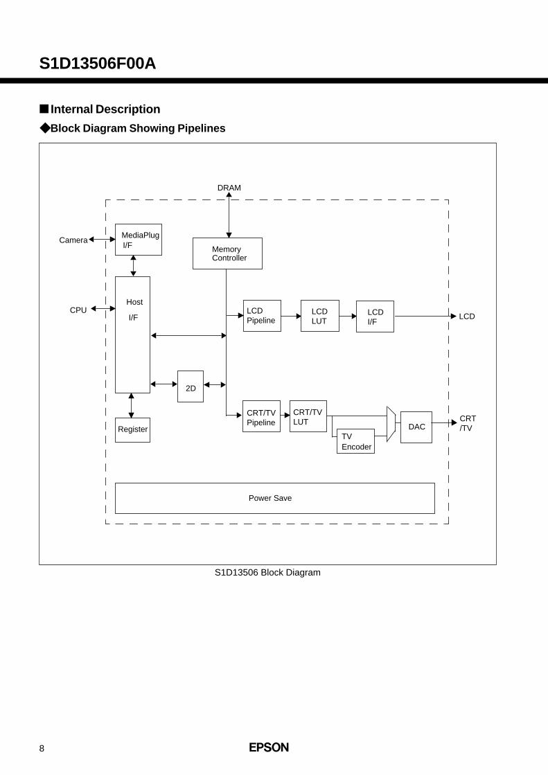
Internal Description
Block Diagram Showing Pipelines
S1D13506 Block Diagram

9
S1D13506F00A
Pins
Pinout Diagram
1 2 3 4 5 6 7 8 9 10 11 12 13 14 15 16 17 18 19 20 21 22 23 24 25 26 27 28 29 30 31 32
96 95 94 93 92 91 90 89 88 87 86 85 84 83 7475 73 72 71 70 69 68 67 66 6582 81 80 79 78 77 76
128
127
126
125
124
123
122
121
120
119
118
117
116
115
114
113
112
111
110
109
108
107
106
105
104
103
102
101
100
99
98
97
33
34
35
36
37
38
39
40
41
42
43
44
45
46
47
48
49
50
58
59
60
61
62
63
51
52
53
54
55
56
57
64
S1D13506F00A
RD
/WR
#
WA
IT#
VD
D
VS
S
DB
15
DB
14
DB
12
DB
8
DB
5
DB
3
DB
2
DB
1
DB
0
DB
13
DB
4
AB
2
RE
SE
T#
VDD
MA6
MA8
DB
7
FP
DAT
3
MA
3
MA
4
MA
2
MA5
MD6
MA11
MA0
MA7
MA10
MA9
VDD
BLUE
VS
S
DACVDD
GREEN
FP
DAT
13
FP
DAT
10
RAS#
WE#
UCAS#
VSS
MD7
MD8
MD5
MD10
MD4
MD11
MD3
MD12
MD2
MD13
MD1
AB3
BS
#
WE
1#
WE
0#
RD
#
M/R
#
CS
#
AB
0
AB
1
AB11
AB12
AB15
AB16
AB17
AB18
AB19
AB20
VDD
VSS
DACVSS
IREF
DACVDD
VDD
FP
DAT
2
FP
DAT
4
VS
S
FP
SH
IFT
NC
FP
LIN
E
FP
FR
AM
E
VS
S
MD15
FP
DAT
15
FP
DAT
14VS
S
DACVDD
MD14
DB
10
DB
9
VS
S
DB
11
DB
6
MA1
LCAS#
MD9
FP
DAT
5
FP
DAT
7
VD
D
TE
ST
EN
FP
DAT
8
MD0
FP
DAT
9
FP
DAT
12
FP
DAT
0
FP
DAT
1
VRTC
FP
DAT
11
HRTC
AB14
AB13
AB7
AB4
AB5
AB8
AB9
AB10
AB6
REDF
PDA
T6
CLK
I
BU
SC
LK
CLK
I2
DACVSS
DR
DY
Pinout Diagram128-pin QFP15 surface mount package

10
S1D13506F00A
Pin Description
Key:I = InputO = OutputIO = Bi-Directional (Input/Output)A = AnalogP = Power pinC = CMOS level inputCD = CMOS level input with pull down resistor (Typ. values of 50kΩ/90kΩ at 5V/3.3V respectively)CS = CMOS level Schmitt inputCOx = CMOS output driver, x denotes driver type (1=4/-4mA, 2=8/-8mA, 3=12/-12mA at 5V)TSx = Tri-state CMOS output driver, x denotes driver type (1=4/-4mA, 2=8/-8mA, 3=12/-12mA at
5V), x denotes driver type (1=4/-4mA, 2=8/-8mA, 3=12/-12mA at 5V)TSu = TSx with pull up resistor (Typ. values of 100kΩ/180kΩ at 5V/3.3V respectively)TSxD = TSx with pull down resistor, x denotes driver type (1=4/-4mA, 2=8/-8mA, 3=12/-12mA at 5V)
(Typ. values of 100kΩ/180kΩ at 5V/3.3V)CNx = CMOS low-noise output driver, x denotes driver type
(1=4/-4mA, 2=8/-8mA, 3=12/-12mA at 5V)CNxU = CNx with pull up resistor, x denotes driver type (1=4/-4mA, 2=8/-8mA, 3=12/-12mA at 5V)CNxD = CNx with pull down resistor, x denotes driver type (1=4/-4mA, 2=8/-8mA, 3=12/-12mA at 5V)
Host Bus InterfaceHost Bus Interface Pin Descriptions
Pin Name Type Pin # CellRESET#
StateDescription
AB0 I 3 CS Hi-Z
• For SH-3/SH-4 Bus, this pin must be connected to VSS or VDD.• For MC68K Bus 1, this pin inputs the lower data strobe (LDS#).• For MC68K Bus 2, this pin inputs system address bit 0 (A0).• For Generic Bus, this pin must be connected to VSS or VDD.• For MIPS/ISA Bus, this pin inputs system address bit 0 (SA0).• For Philips PR31500/31700 Bus, this pin inputs system
address bit 0 (A0).• For Toshiba TX3912 Bus, this pin inputs system address bit 0 (A0).• For PowerPC Bus, this pin inputs system address bit 31 (A31).• For PC Card (PCMCIA) Bus, this pin must be connected to VSS
or VDD.
AB[12:1] I119-128,
1, 2C Hi-Z
• For PowerPC Bus, these pins input the system address bits 19 through 30 (A[19:30]).
• For all other busses, these pins input the system address bits 12 through 1 (A[12:1]).
See Table “CPU Interface Pin Mapping” on page 21 for summary. See the respective AC Timing diagram for detailed functionality.
See Table “CPU Interface Pin Mapping” on page 21 for summary. See the respective ACTiming diagram for detailed functionality
11
S1D13506F00A
Host Bus Interface Pin Descriptions
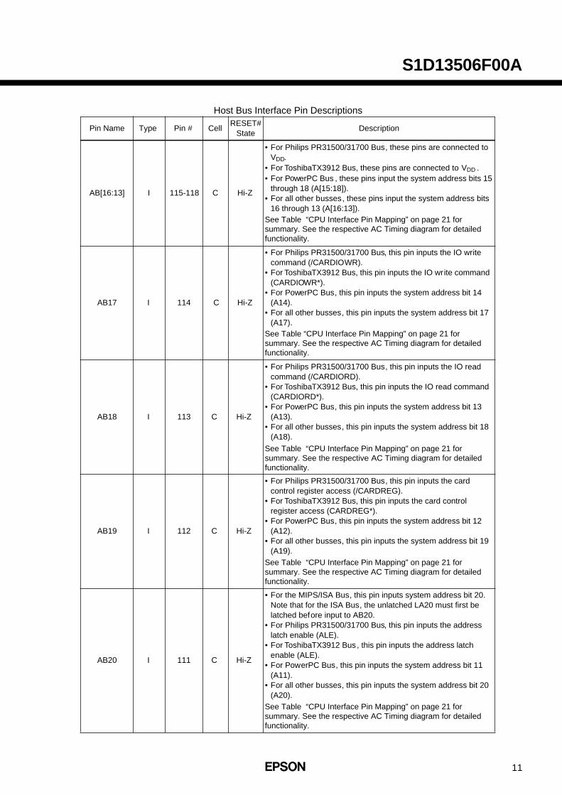
AB[16:13] I 115-118 C Hi-Z
• For Philips PR31500/31700 Bus, these pins are connected to VDD.
• For Toshiba TX3912 Bus, these pins are connected to VDD .• For PowerPC Bus , these pins input the system address bits 15
through 18 (A[15:18]).• For all other busses, these pins input the system address bits
16 through 13 (A[16:13]).
AB17 I 114 C Hi-Z
• For Philips PR31500/31700 Bus, this pin inputs the IO write command (/CARDIOWR).
• For Toshiba TX3912 Bus, this pin inputs the IO write command (CARDIOWR*).
• For PowerPC Bus, this pin inputs the system address bit 14 (A14).
• For all other busses, this pin inputs the system address bit 17 (A17).
AB18 I 113 C Hi-Z
• For Philips PR31500/31700 Bus, this pin inputs the IO read command (/CARDIORD).
• For Toshiba TX3912 Bus, this pin inputs the IO read command (CARDIORD*).
• For PowerPC Bus, this pin inputs the system address bit 13 (A13).
• For all other busses, this pin inputs the system address bit 18 (A18).
AB19 I 112 C Hi-Z
• For Philips PR31500/31700 Bus, this pin inputs the card control register access (/CARDREG).
• For Toshiba TX3912 Bus, this pin inputs the card control register access (CARDREG*).
• For PowerPC Bus, this pin inputs the system address bit 12 (A12).
• For all other busses, this pin inputs the system address bit 19 (A19).
AB20 I 111 C Hi-Z
• For the MIPS/ISA Bus, this pin inputs system address bit 20. Note that for the ISA Bus, the unlatched LA20 must first be latched before input to AB20.
• For Philips PR31500/31700 Bus, this pin inputs the address latch enable (ALE).
• For Toshiba TX3912 Bus , this pin inputs the address latch enable (ALE).
• For PowerPC Bus, this pin inputs the system address bit 11 (A11).
• For all other busses, this pin inputs the system address bit 20 (A20).
Pin Name Type Pin # CellRESET#
StateDescription
See Table “CPU Interface Pin Mapping” on page 21 forsummary. See the respective AC Timing diagram for detailed functionality.
See Table “CPU Interface Pin Mapping” on page 21 forsummary. See the respective AC Timing diagram for detailed functionality.
See Table “CPU Interface Pin Mapping” on page 21 for summary. See the respective AC Timing diagram for detailed functionality.
See Table “CPU Interface Pin Mapping” on page 21 for summary. See the respective AC Timing diagram for detailed functionality.
See Table “CPU Interface Pin Mapping” on page 21 for summary. See the respective AC Timing diagram for detailed functionality.
12
S1D13506F00A
Host Bus Interface Pin Descriptions (Continued)
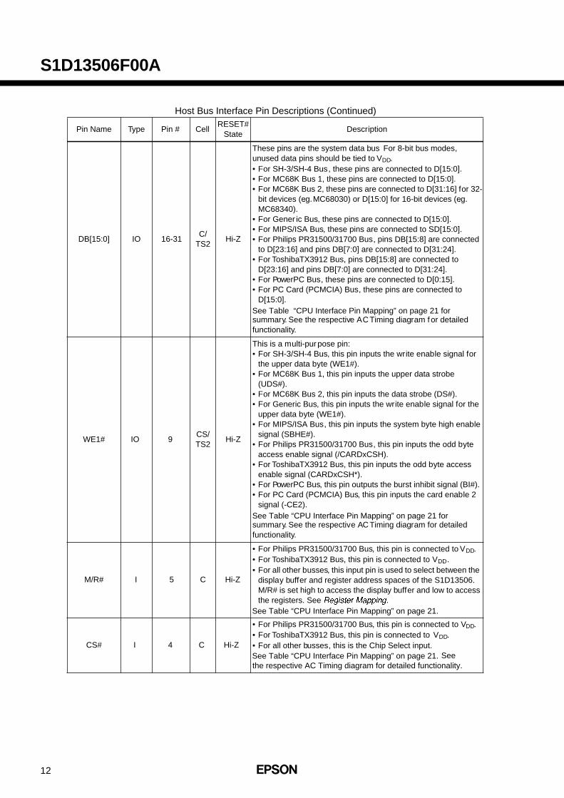
DB[15:0] IO 16-31C/
TS2Hi-Z
These pins are the system data bus. For 8-bit bus modes, unused data pins should be tied to VDD.• For SH-3/SH-4 Bus, these pins are connected to D[15:0].• For MC68K Bus 1, these pins are connected to D[15:0].• For MC68K Bus 2, these pins are connected to D[31:16] for 32-
bit devices (e.g. MC68030) or D[15:0] for 16-bit devices (e.g. MC68340).
• For Gener ic Bus, these pins are connected to D[15:0].• For MIPS/ISA Bus, these pins are connected to SD[15:0].• For Philips PR31500/31700 Bus, pins DB[15:8] are connected
to D[23:16] and pins DB[7:0] are connected to D[31:24].• For Toshiba TX3912 Bus, pins DB[15:8] are connected to
D[23:16] and pins DB[7:0] are connected to D[31:24].• For PowerPC Bus, these pins are connected to D[0:15].• For PC Card (PCMCIA) Bus, these pins are connected to
D[15:0].
summary. See the respective AC Timing diagram for detailed functionality.
WE1# IO 9CS/TS2
Hi-Z
This is a multi-pur pose pin:• For SH-3/SH-4 Bus, this pin inputs the write enable signal for
the upper data byte (WE1#).• For MC68K Bus 1, this pin inputs the upper data strobe
(UDS#).• For MC68K Bus 2, this pin inputs the data strobe (DS#).• For Generic Bus, this pin inputs the write enable signal for the
upper data byte (WE1#).• For MIPS/ISA Bus, this pin inputs the system byte high enable
signal (SBHE#).• For Philips PR31500/31700 Bus, this pin inputs the odd byte
access enable signal (/CARDxCSH).• For Toshiba TX3912 Bus, this pin inputs the odd byte access
enable signal (CARDxCSH*).• For PowerPC Bus, this pin outputs the burst inhibit signal (BI#).• For PC Card (PCMCIA) Bus, this pin inputs the card enable 2
signal (-CE2).
summary. See the respective AC Timing diagram for detailed functionality.
M/R# I 5 C Hi-Z
• For Philips PR31500/31700 Bus, this pin is connected to VDD.• For Toshiba TX3912 Bus, this pin is connected to VDD.• For all other busses, this input pin is used to select between the
display buffer and register address spaces of the S1D13506. M/R# is set high to access the display buffer and low to access the registers. See Register Mapping.
CS# I 4 C Hi-Z
• For Philips PR31500/31700 Bus, this pin is connected to VDD.• For Toshiba TX3912 Bus, this pin is connected to VDD.• For all other busses, this is the Chip Select input.
See the respective AC Timing diagram for detailed functionality.
Pin Name Type Pin # CellRESET#
StateDescription
See Table “CPU Interface Pin Mapping” on page 21 for
See Table “CPU Interface Pin Mapping” on page 21 for
See Table “CPU Interface Pin Mapping” on page 21.
See Table “CPU Interface Pin Mapping” on page 21.
13
S1D13506F00A
Host Bus Interface Pin Descriptions (Continued)
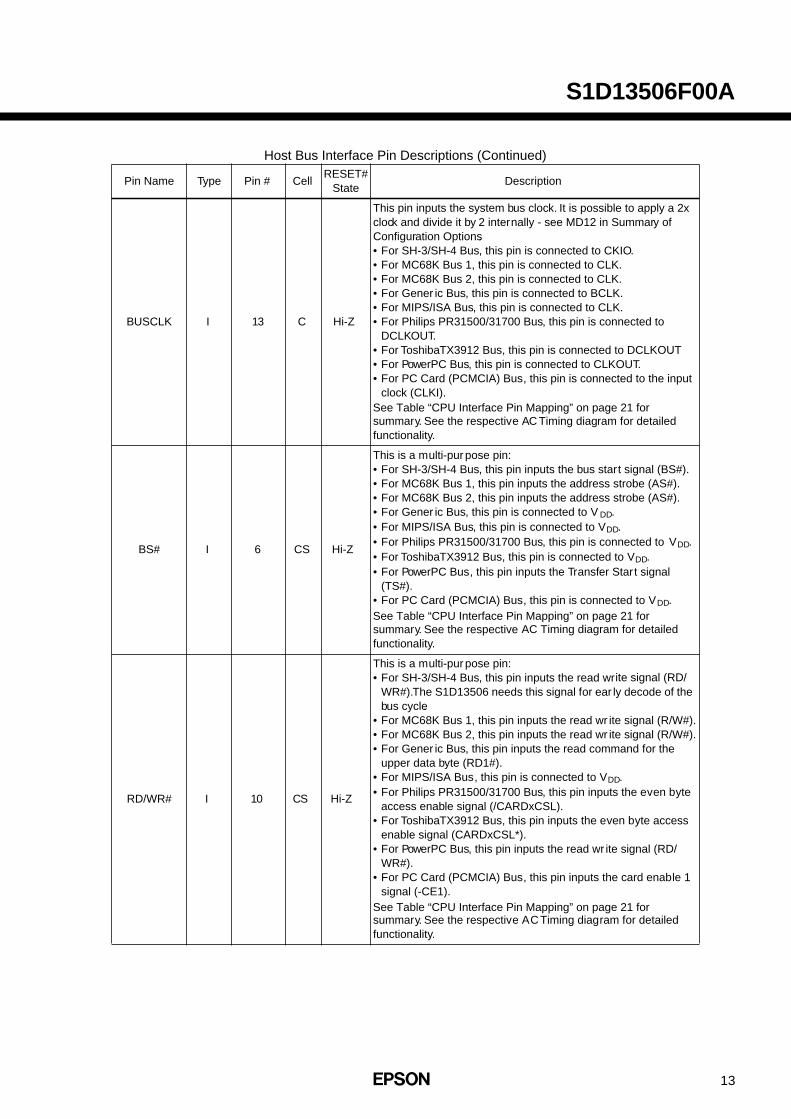
BUSCLK I 13 C Hi-Z
This pin inputs the system bus clock. It is possible to apply a 2x clock and divide it by 2 internally - see MD12 in Summary of Configuration Options.• For SH-3/SH-4 Bus, this pin is connected to CKIO.• For MC68K Bus 1, this pin is connected to CLK.• For MC68K Bus 2, this pin is connected to CLK.• For Gener ic Bus, this pin is connected to BCLK.• For MIPS/ISA Bus, this pin is connected to CLK.• For Philips PR31500/31700 Bus, this pin is connected to
DCLKOUT.• For Toshiba TX3912 Bus, this pin is connected to DCLKOUT.• For PowerPC Bus, this pin is connected to CLKOUT. • For PC Card (PCMCIA) Bus, this pin is connected to the input
clock (CLKI).
summary. See the respective AC Timing diagram for detailed functionality.
BS# I 6 CS Hi-Z
This is a multi-pur pose pin:• For SH-3/SH-4 Bus, this pin inputs the bus start signal (BS#).• For MC68K Bus 1, this pin inputs the address strobe (AS#).• For MC68K Bus 2, this pin inputs the address strobe (AS#).• For Gener ic Bus, this pin is connected to V DD.• For MIPS/ISA Bus, this pin is connected to VDD. • For Philips PR31500/31700 Bus, this pin is connected to VDD.• For Toshiba TX3912 Bus, this pin is connected to VDD.• For PowerPC Bus, this pin inputs the Transfer Start signal
(TS#).• For PC Card (PCMCIA) Bus, this pin is connected to VDD.
summary. See the respectivefunctionality.
RD/WR# I 10 CS Hi-Z
This is a multi-pur pose pin:• For SH-3/SH-4 Bus, this pin inputs the read write signal (RD/
WR#). The S1D13506 needs this signal for ear ly decode of the bus cycle.
• For MC68K Bus 1, this pin inputs the read wr ite signal (R/W#).• For MC68K Bus 2, this pin inputs the read wr ite signal (R/W#).• For Gener ic Bus, this pin inputs the read command for the
upper data byte (RD1#).• For MIPS/ISA Bus, this pin is connected to VDD.• For Philips PR31500/31700 Bus, this pin inputs the even byte
access enable signal (/CARDxCSL).• For Toshiba TX3912 Bus, this pin inputs the even byte access
enable signal (CARDxCSL*).• For PowerPC Bus, this pin inputs the read wr ite signal (RD/
WR#).• For PC Card (PCMCIA) Bus, this pin inputs the card enable 1
signal (-CE1).
summary. See the respective AC Timing diagram for detailed functionality.
Pin Name Type Pin # CellRESET#
State
See Table “CPU Interface Pin Mapping” on page 21 for
See Table “CPU Interface Pin Mapping” on page 21 for
See Table “CPU Interface Pin Mapping” on page 21 for
Description
AC Timing diagram for detailed
14
S1D13506F00A
Host Bus Interface Pin Descriptions (Continued)
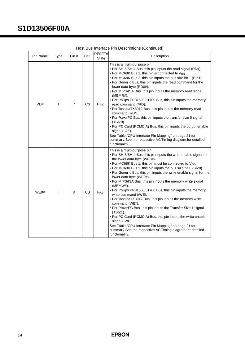
RD# I 7 CS Hi-Z
This is a multi-pur pose pin:• For SH-3/SH-4 Bus, this pin inputs the read signal (RD#).• For MC68K Bus 1, this pin is connected to VDD.• For MC68K Bus 2, this pin inputs the bus size bit 1 (SIZ1).• For Gener ic Bus, this pin inputs the read command for the
lower data byte (RD0#).• For MIPS/ISA Bus, this pin inputs the memory read signal
(MEMR#).• For Philips PR31500/31700 Bus, this pin inputs the memory
read command (/RD).• For Toshiba TX3912 Bus, this pin inputs the memory read
command (RD*).• For PowerPC Bus, this pin inputs the transfer size 0 signal
(TSIZ0).• For PC Card (PCMCIA) Bus, this pin inputs the output enable
signal (-OE).
summary. See the respective AC Timing diagram for detailed functionality.
WE0# I 8 CS Hi-Z
This is a multi-pur pose pin:• For SH-3/SH-4 Bus, this pin inputs the write enable signal for
the lower data byte (WE0#).• For MC68K Bus 1, this pin must be connected to VDD
• For MC68K Bus 2, this pin inputs the bus size bit 0 (SIZ0).• For Gener ic Bus, this pin inputs the write enable signal for the
lower data byte (WE0#).• For MIPS/ISA Bus, this pin inputs the memory write signal
(MEMW#).• For Philips PR31500/31700 Bus, this pin inputs the memory
write command (/WE).• For Toshiba TX3912 Bus, this pin inputs the memory write
command (WE*).• For PowerPC Bus, this pin inputs the Transfer Size 1 signal
(TSIZ1).• For PC Card (PCMCIA) Bus, this pin inputs the write enable
signal (-WE).
summary. See the respective AC Timing diagram for detailed functionality.
Pin Name Type Pin # CellRESET#
StateDescription
See Table “CPU Interface Pin Mapping” on page 21 for
See Table “CPU Interface Pin Mapping” on page 21 for
15
S1D13506F00A
Host Bus Interface Pin Descriptions (Continued)
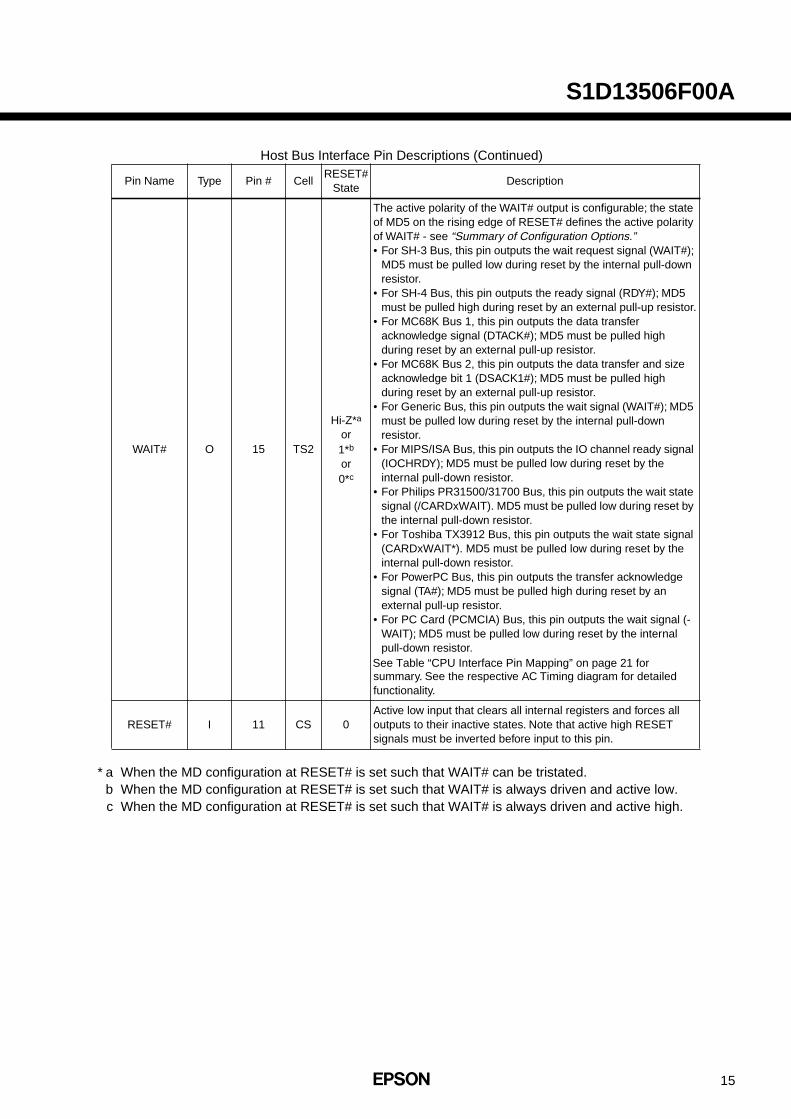
* a When the MD configuration at RESET# is set such that WAIT# can be tristated.b When the MD configuration at RESET# is set such that WAIT# is always driven and active low.c When the MD configuration at RESET# is set such that WAIT# is always driven and active high.
WAIT# O 15 TS2
Hi-Z*a
or1*b
or0*c
The active polarity of the WAIT# output is configurable; the state of MD5 on the rising edge of RESET# defines the active polarity of WAIT# - see “Summary of Configuration Options.”• For SH-3 Bus, this pin outputs the wait request signal (WAIT#);
MD5 must be pulled low during reset by the internal pull-down resistor.
• For SH-4 Bus, this pin outputs the ready signal (RDY#); MD5 must be pulled high during reset by an external pull-up resistor.
• For MC68K Bus 1, this pin outputs the data transfer acknowledge signal (DTACK#); MD5 must be pulled high during reset by an external pull-up resistor.
• For MC68K Bus 2, this pin outputs the data transfer and size acknowledge bit 1 (DSACK1#); MD5 must be pulled high during reset by an external pull-up resistor.
• For Generic Bus, this pin outputs the wait signal (WAIT#); MD5 must be pulled low during reset by the internal pull-down resistor.
• For MIPS/ISA Bus, this pin outputs the IO channel ready signal (IOCHRDY); MD5 must be pulled low during reset by the internal pull-down resistor.
• For Philips PR31500/31700 Bus, this pin outputs the wait state signal (/CARDxWAIT). MD5 must be pulled low during reset by the internal pull-down resistor.
• For Toshiba TX3912 Bus, this pin outputs the wait state signal (CARDxWAIT*). MD5 must be pulled low during reset by the internal pull-down resistor.
• For PowerPC Bus, this pin outputs the transfer acknowledge signal (TA#); MD5 must be pulled high during reset by an external pull-up resistor.
• For PC Card (PCMCIA) Bus, this pin outputs the wait signal (-WAIT); MD5 must be pulled low during reset by the internal pull-down resistor.
summary. See the respective AC Timing diagram for detailed functionality.
RESET# I 11 CS 0Active low input that clears all internal registers and forces all outputs to their inactive states. Note that active high RESET signals must be inverted before input to this pin.
Pin Name Type Pin # CellRESET#
StateDescription
See Table “CPU Interface Pin Mapping” on page 21 for
16
S1D13506F00A
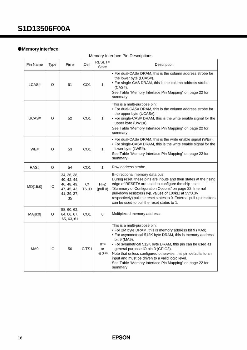
Memory InterfaceMemory Interface Pin Descriptions
Pin Name Type Pin # CellRESET#
StateDescription
LCAS# O 51 CO1 1
• For dual-CAS# DRAM, this is the column address strobe for the lower byte (LCAS#).
• For single-CAS DRAM, this is the column address strobe (CAS#).
summary.
UCAS# O 52 CO1 1
This is a multi-purpose pin:• For dual-CAS# DRAM, this is the column address strobe for
the upper byte (UCAS#).• For single-CAS# DRAM, this is the write enable signal for the
upper byte (UWE#).
WE# O 53 CO1 1
• For dual-CAS# DRAM, this is the write enable signal (WE#).• For single-CAS# DRAM, this is the write enable signal for the
lower byte (LWE#).
RAS# O 54 CO1 1 Row address strobe.
MD[15:0] IO
34, 36, 38, 40, 42, 44, 46, 48, 49, 47, 45, 43, 41, 39, 37,
35
C/TS1D
Hi-Z(pull 0)
Bi-directional memory data bus. During reset, these pins are inputs and their states at the rising edge of RESET# are used to configure the chip - see “Summary of Configuration Options” on page 22. Internal pull-down resistors (Typ. values of 100kΩ at 5V/3.3V respectively) pull the reset states to 0. External pull-up resistors can be used to pull the reset states to 1.
MA[8:0] O58, 60, 62, 64, 66, 67, 65, 63, 61
CO1 0 Multiplexed memory address.
MA9 IO 56 C/TS10*a
orHi-Z*b
This is a multi-purpose pin:• For 2M byte DRAM, this is memory address bit 9 (MA9).• For asymmetrical 512K byte DRAM, this is memory address
bit 9 (MA9).• For symmetrical 512K byte DRAM, this pin can be used as
general purpose IO pin 3 (GPIO3). Note that unless configured otherwise, this pin defaults to an input and must be driven to a valid logic level.
See Table “Memory Interface Pin Mapping” on page 22 for
summary.See Table “Memory Interface Pin Mapping” on page 22 for
summary.See Table “Memory Interface Pin Mapping” on page 22 for
summary.See Table “Memory Interface Pin Mapping” on page 22 for
17
S1D13506F00A
Memory Interface Pin Descriptions
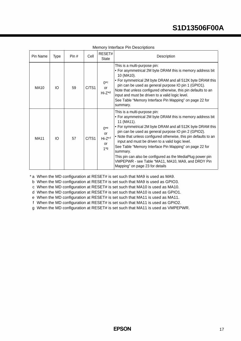
* a When the MD configuration at RESET# is set such that MA9 is used as MA9.b When the MD configuration at RESET# is set such that MA9 is used as GPIO3.c When the MD configuration at RESET# is set such that MA10 is used as MA10.d When the MD configuration at RESET# is set such that MA10 is used as GPIO1.e When the MD configuration at RESET# is set such that MA11 is used as MA11.f When the MD configuration at RESET# is set such that MA11 is used as GPIO2.g When the MD configuration at RESET# is set such that MA11 is used as VMPEPWR.
MA10 IO 59 C/TS10*c
orHi-Z*d
This is a multi-purpose pin:• For asymmetrical 2M byte DRAM this is memory address bit
10 (MA10).• For symmetrical 2M byte DRAM and all 512K byte DRAM this
pin can be used as general purpose IO pin 1 (GPIO1). Note that unless configured otherwise, this pin defaults to an input and must be driven to a valid logic level.
MA11 IO 57 C/TS1
0*e
orHi-Z* f
or1*g
This is a multi-purpose pin:• For asymmetrical 2M byte DRAM this is memory address bit
11 (MA11).• For symmetrical 2M byte DRAM and all 512K byte DRAM this
pin can be used as general purpose IO pin 2 (GPIO2).• Note that unless configured otherwise, this pin defaults to an
input and must be driven to a valid logic level.
Pin Name Type Pin # CellRESET#
StateDescription
See Table “Memory Interface Pin Mapping” on page 22 for summary.
See Table “Memory Interface Pin Mapping” on page 22 for summary.This pin can also be configured as the MediaPlug power pin VMPEPWR - see Table “MA11, MA10, MA9, and DRDY Pin Mapping” on page 23 for details

18
S1D13506F00A
LCD Interface
LCD Interface Pin Descriptions
* a When the MD configuration at RESET# is set such that FPDAT9 is used as FPDAT9.b When the MD configuration at RESET# is set such that FPDAT9 is used as VMPRCTL.c When the MD configuration at RESET# is set such that FPDAT[13:10] is used as FPDAT[13:10].d When the MD configuration at RESET# is set such that FPDAT[13:10] is used as VMPD[3:0].e When the MD configuration at RESET# is set such that DRDY is used as DRDY (MOD).f When the MD configuration at RESET# is set such that DRDY is used as VMPEPWR.
Pin Name Type Pin # CellRESET#
StateDescription
FPDAT[8:0] O 88, 86-79 CN3 0
FPDAT9 O 89 CN3D0*a
orHi-Z*b
FPDAT[13:10] IO 93-90C/
TS3U
0*c
orHi-Z*d
FPDAT[15:14] O 95,94 CN3 0
FPFRAME O 73 CN3 0 Frame pulse
FPLINE O 74 CN3 0 Line pulse
FPSHIFT O 77 CO3 0 Shift clock
DRDY O 76 CO30*e
or1*f
This is a multi-purpose pin:• For TFT/D-TFD panels this is the display enable output
(DRDY).• For passive LCD with Format 1 interface this is the 2nd
Shift Clock (FPSHIFT2).• For all other LCD panels this is the LCD backplane bias
signal (MOD).
This pin can also be configured as the MediaPlug power pin VMPEPWR - see Table “MA11, MA10, MA9, and DRDY Pin Mapping” on page 23 for details.
Panel data bus. Not all pins are used for some panels - see Table “LCD Interface Pin Mapping” on page 22 for details. Unused pins are driven low. FPDAT[15:8] can be configured for MediaPlug interface - see Table “MediaPlugInterface Pin Mapping” on page 23 for details.
Panel data bus. Not all pins are used for some panels - see Table “LCD Interface Pin Mapping” on page 22 for details. Unused pins are driven low. FPDAT[15:8] can be configured for MediaPlug interface - see Table “MediaPlug Interface Pin Mapping” on page 23 for details.
Panel data bus. Not all pins are used for some panels - see Table “LCD Interface Pin Mapping” on page 22 for details. Unused pins are driven low. FPDAT[15:8] can be configured for MediaPlug interface - see Table “MediaPlug Interface Pin Mapping” on page 23 for details.
Panel data bus. Not all pins are used for some panels - see Table “LCD Interface Pin Mapping” on page 22 for details. Unused pins are driven low. FPDAT[15:8] can be configured for MediaPlug interface - see Table “MediaPlug Interface Pin Mapping” on page 23 for details.
See Table “LCD Interface Pin Mapping” on page 22 andREG[030h] for details.
19
S1D13506F00A
CRT Interface
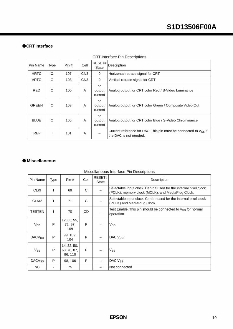
CRT Interface Pin Descriptions
Miscellaneous
Miscellaneous Interface Pin Descriptions
Pin Name Type Pin # CellRESET#
StateDescription
HRTC O 107 CN3 0 Horizontal retrace signal for CRT
VRTC O 108 CN3 0 Vertical retrace signal for CRT
RED O 100 Ano
output current
Analog output for CRT color Red / S-Video Luminance
GREEN O 103 Ano
output current
Analog output for CRT color Green / Composite Video Out
BLUE O 105 Ano
output current
Analog output for CRT color Blue / S-Video Chrominance
IREF I 101 A –Current reference for DAC. This pin must be connected to VSS if the DAC is not needed.
Pin Name Type Pin # CellRESET#
StateDescription
CLKI I 69 C –Selectable input clock. Can be used for the internal pixel clock (PCLK), memory clock (MCLK), and MediaPlug Clock.
CLKI2 I 71 C –Selectable input clock. Can be used for the internal pixel clock (PCLK) and MediaPlug Clock.
TESTEN I 70 CD –Test Enable. This pin should be connected to VSS for normal operation.
VDD P12, 33, 55,
72, 97, 109
P – VDD
DACVDD P99, 102,
104P – DAC VDD
VSS P14, 32, 50, 68, 78, 87,
96, 110P – VSS
DACVSS P 98, 106 P – DAC VSS
NC - 75 – Not connected
20
S1D13506F00A
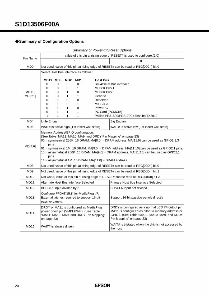
Summary of Configuration Options
Summary of Power-On/Reset Options
Pin Namevalue of this pin at rising edge of RESET# is used to configure:(1/0)
1 0
MD0 Not used, value of this pin at rising edge of RESET# can be read at REG[00Ch] bit 0
MD11, MD[3:1]
Select Host Bus Interface as follows :
MD11 MD3 MD2 MD1 Host Bus 0 0 0 0 SH-4/SH-3 Bus interface 0 0 0 1 MC68K Bus 1 0 0 1 0 MC68K Bus 2 0 0 1 1 Generic 0 1 0 0 Reserved 0 1 0 1 MIPS/ISA 0 1 1 0 PowerPC 0 1 1 1 PC Card (PCMCIA) 1 1 1 1 Philips PR31500/PR31700 / Toshiba TX3912
MD4 Little Endian Big Endian
MD5 WAIT# is active high (1 = insert wait state) WAIT# is active low (0 = insert wait state)
MD[7:6]
Memory Address/GPIO configuration:(See Table “MA11, MA10, MA9, and DRDY Pin Mapping” on page 23) 00 = symmetrical 256K 16 DRAM. MA[8:0] = DRAM address. MA[11:9] can be used as GPIO2,1,3
pins .01 = symmetrical 1M 16 DRAM. MA[9:0] = DRAM address. MA[11:10] can be used as GPIO2,1 pins.10 = asymmetrical 256K 16 DRAM. MA[9:0] = DRAM address. MA[11:10] can be used as GPIO2,1
pins.11 = asymmetrical 1M 16 DRAM. MA[11:0] = DRAM address.
MD8 Not used, value of this pin at rising edge of RESET# can be read at REG[00Dh] bit 0
MD9 Not used, value of this pin at rising edge of RESET# can be read at REG[00Dh] bit 1
MD10 Not Used, value of this pin at rising edge of RESET# can be read at REG[00Dh] bit 2
MD11 Alternate Host Bus Interface Selected Primary Host Bus Interface Selected
MD12 BUSCLK input divided by 2 BUSCLK input not divided
MD13Configure FPDAT[15:8] for MediaPlug I/F. External latches required to support 16-bit passive panels.
Support 16-bit passive panels directly
MD14
MD15 WAIT# is always drivenWAIT# is tristated when the chip is not accessed by the host
DRDY or MA11 is configured as MediaPlug power down pin (VMPEPWR). (See Table “MA11, MA10, MA9, and DRDY Pin Mapping”on page 23)
DRDY is configured as a normal LCD I/F output pin.MA11 is configur ed as either a memory address or GPIO2. (See Table “MA11, MA10, MA9, and DRDY Pin Mapping” on page 23)
21
S1D13506F00A
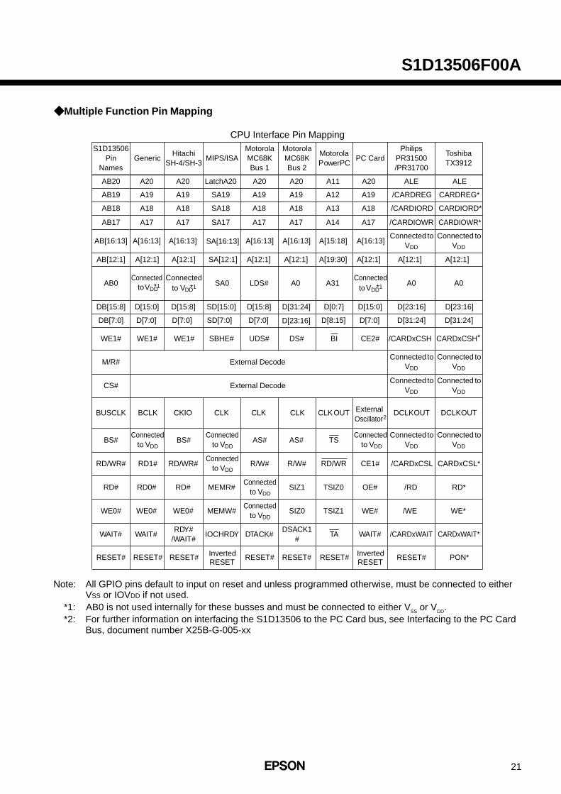
Multiple Function Pin Mapping
CPU Interface Pin Mapping
Note: All GPIO pins default to input on reset and unless programmed otherwise, must be connected to eitherVSS or IOVDD if not used.
*1: AB0 is not used internally for these busses and must be connected to either VSS or VDD. *2: For further information on interfacing the S1D13506 to the PC Card bus, see Interfacing to the PC Card
Bus, document number X25B-G-005-xx
S1D13506Pin
NamesGeneric
Hitachi SH-4/SH-3
MIPS/ISAMotorola MC68K Bus 1
Motorola MC68K Bus 2
Motorola PowerPC
PC CardPhilips
PR31500/PR31700
Toshiba TX3912
AB20 A20 A20 LatchA20 A20 A20 A11 A20 ALE ALE
AB19 A19 A19 SA19 A19 A19 A12 A19 /CARDREG CARDREG*
AB18 A18 A18 SA18 A18 A18 A13 A18 /CARDIORD CARDIORD*
AB17 A17 A17 SA17 A17 A17 A14 A17 /CARDIOWR CARDIOWR*
AB[16:13] A[16:13] A[16:13]
SA[16:13] A[16:13] A[16:13] A[15:18] A[16:13]Connected to
VDD
Connected to VDD
AB[12:1] A[12:1] A[12:1] SA[12:1] A[12:1] A[12:1] A[19:30] A[12:1] A[12:1] A[12:1]
AB0Connected
to VDD1Connected
VDD1 SA0 LDS# A0 A31Connected
to VDD1 A0 A0
DB[15:8] D[15:0] D[15:8] SD[15:0] D[15:8] D[31:24] D[0:7] D[15:0] D[23:16] D[23:16]
DB[7:0] D[7:0] D[7:0] SD[7:0] D[7:0] D[23:16] D[8:15] D[7:0] D[31:24] D[31:24]
WE1# WE1# WE1# SBHE# UDS# DS# BI CE2# /CARDxCSH CARDxCSH*
M/R# External DecodeConnected to
VDD
Connected to VDD
CS# External DecodeConnected to
VDD
Connected to VDD
BUSCLK BCLK CKIO CLK CLK CLK CLKOUT External Oscillator2
DCLKOUT DCLKOUT
BS#Connected
to VDDBS#
Connected to VDD
AS# AS# TSConnected
to VDD
Connected to VDD
Connected to VDD
RD/WR# RD1# RD/WR#Connected
to VDDR/W# R/W# RD/WR CE1# /CARDxCSL CARDxCSL*
RD# RD0# RD# MEMR#Connected
to VDDSIZ1 TSIZ0 OE# /RD RD*
WE0# WE0# WE0# MEMW#Connected
to VDDSIZ0 TSIZ1 WE# /WE WE*
WAIT# WAIT#RDY#
/WAIT#IOCHRDY DTACK#
DSACK1#
TA WAIT# /CARDxWAIT CARDxWAIT*
RESET# RESET# RESET#RESET
RESET# RESET# RESET#RESET
RESET# PON*
to
Inverted Inverted
* * *

22
S1D13506F00A
Memory Interface Pin Mapping
*1 For MA9, MA10, and MA11 functionality see Table “MA11, MA10, MA9, and DRDY Pin Mapping” on page23.
*2 All GPIO pins default to input on reset and unless programmed otherwise, should be connected to eitherV
SS or IOVDD if not used.
LCD Interface Pin Mapping
Note: DRDY and FPDAT[15:8] may be used by the MediaPlug interface when the MediaPlug is enabled. For MediaPlug Interfacepin mapping, see Table “MediaPlug Interface Pin Mapping.”
S1D13506Pin Names
FPM/EDO-DRAM
Sym 256Kx16 Asym 256Kx16 Sym 1Mx16 Asym 1Mx16
2-CAS# 2-WE# 2-CAS# 2-WE# 2-CAS# 2-WE# 2-CAS# 2-WE#
MD[15:0] D[15:0]
MA[8:0] A[8:0]
MA9*1 GPIO3*2 A9 A9
MA10*1 GPIO12 A10
MA11*1 GPIO22 A11
UCAS# UCAS# UWE# UCAS# UWE# UCAS# UWE# UCAS# UWE#
LCAS# LCAS# CAS# LCAS# CAS# LCAS# CAS# LCAS# CAS#
WE# WE# LWE# WE# LWE# WE# LWE# WE# LWE#
RAS# RAS#
S1D13506Pin
Names
Monochrome Passive Panel
Color Passive PanelColor TFT/D-TFD Panel
Single Dual Single SingleFormat 1
SingleFormat 2
Single Dual
4-bit 8-bit 8-bit 4-bit 8-bit 8-bit 16-Bit 8-bit 16-bit 9-bit 12-bit 18-bit
FPFRAME
FPLINE FPLINE
FPSHIFT FPSHIFT
DRDY MODFPSHI
FT2MOD DRDY
FPDAT0driven
0D0 LD0
driven 0
D0 D0 D0 LD0 LD0 R2 R3 R5
FPDAT1driven
0D1 LD1
driven 0
D1 D1 D1 LD1 LD1 R1 R2 R4
FPDAT2driven
0D2 LD2
driven 0
D2 D2 D2 LD2 LD2 R0 R1 R3
FPDAT3driven
0D3 LD3
driven 0
D3 D3 D3 LD3 LD3 G2 G3 G5
FPDAT4 D0 D4 UD0 D0 D4 D4 D4 UD0 UD0 G1 G2 G4
FPDAT5 D1 D5 UD1 D1 D5 D5 D5 UD1 UD1 G0 G1 G3
FPDAT6 D2 D6 UD2 D2 D6 D6 D6 UD2 UD2 B2 B3 B5
FPDAT7 D3 D7 UD3 D3 D7 D7 D7 UD3 UD3 B1 B2 B4
FPDAT8driven
0driven
0driven
0driven
0driven
0driven
0D8
driven 0
LD4 B0 B1 B3
FPDAT9driven
0driven
0driven
0driven
0driven
0driven
0D9
driven 0
LD5driven
0R0 R2
FPDAT10driven
0driven
0driven
0driven
0driven
0driven
0D10
driven 0
LD6driven
0driven
0R1
FPDAT11driven
0driven
0driven
0driven
0driven
0driven
0D11
driven 0
LD7driven
0G0 G2
FPDAT12driven
0driven
0driven
0driven
0driven
0driven
0D12
driven 0
UD4driven
0driven
0G1
FPDAT13driven
0driven
0driven
0driven
0driven
0driven
0D13
driven 0
UD5driven
0driven
0G0
FPDAT14driven
0driven
0driven
0driven
0driven
0driven
0D14
driven 0
UD6driven
0B0 B2
FPDAT15driven
0driven
0driven
0driven
0driven
0driven
0D15
driven 0
UD7driven
0driven
0B1
FPFRAME
23
S1D13506F00A
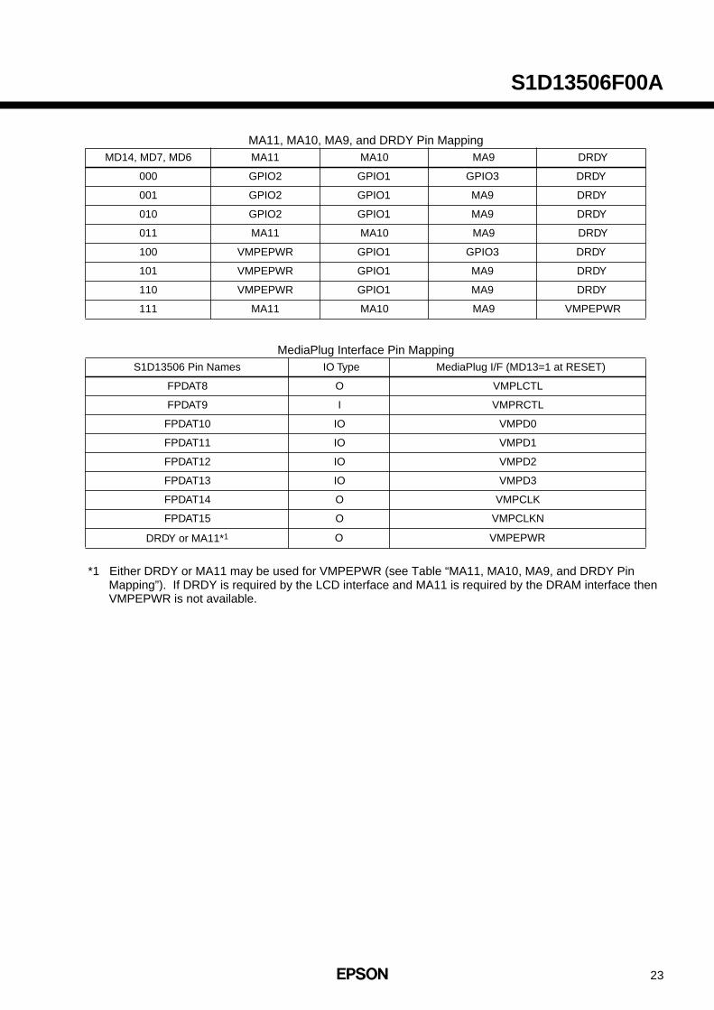
MA11, MA10, MA9, and DRDY Pin Mapping
MediaPlug Interface Pin Mapping
*1 Either DRDY or MA11 may be used for VMPEPWR (see Table “MA11, MA10, MA9, and DRDY PinMapping”). If DRDY is required by the LCD interface and MA11 is required by the DRAM interface thenVMPEPWR is not available.
MD14, MD7, MD6 MA11 MA10 MA9 DRDY
000 GPIO2 GPIO1 GPIO3 DRDY
001 GPIO2 GPIO1 MA9 DRDY
010 GPIO2 GPIO1 MA9 DRDY
011 MA11 MA10 MA9 DRDY
100 VMPEPWR GPIO1 GPIO3 DRDY
101 VMPEPWR GPIO1 MA9 DRDY
110 VMPEPWR GPIO1 MA9 DRDY
111 MA11 MA10 MA9 VMPEPWR
S1D13506 Pin Names IO Type MediaPlug I/F (MD13=1 at RESET)
FPDAT8 O VMPLCTL
FPDAT9 I VMPRCTL
FPDAT10 IO VMPD0
FPDAT11 IO VMPD1
FPDAT12 IO VMPD2
FPDAT13 IO VMPD3
FPDAT14 O VMPCLK
FPDAT15 O VMPCLKN
DRDY or MA11*1 O VMPEPWR
24
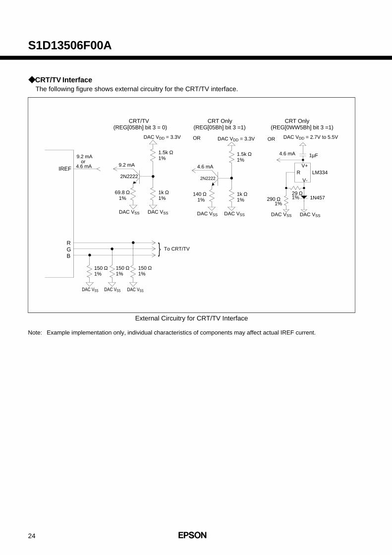
S1D13506F00A
2N2222
4.6 mA 9.2 mA
69.8 Ω1%
1k Ω1%
1.5k Ω1%
DAC VSS DAC VSS
DAC VDD = 3.3V
150 Ω1%
150 Ω1%
150 Ω1%
DAC VSS DAC VSS DAC VSS
IREF
RGB
To CRT/TV
2N2222
4.6 mA
140 Ω1%
1k Ω1%
1.5k Ω1%
DAC VSS DAC VSS
DAC VDD = 3.3VOR
CRT/TV CRT Only
or9.2 mA
V+R
V-
DAC VSS DAC VSS
DAC VDD = 2.7V to 5.5V
LM334
290 Ω1%
29 Ω1% 1N457
1µF4.6 mA
OR
(REG[05Bh] bit 3 = 0) (REG[05Bh] bit 3 =1)CRT Only
(REG[0WW5Bh] bit 3 =1)
CRT/TV InterfaceThe following figure shows external circuitry for the CRT/TV interface.
External Circuitry for CRT/TV Interface
Note: Example implementation only, individual characteristics of components may affect actual IREF current.

25
S1D13506F00A
D.C. Characteristics
Absolute Maximum Ratings
Recommended Operating Conditions
Electrical Characteristics for VDD
= 5.0V typical
Symbol Parameter Rating Units
VDD Supply Voltage VSS - 0.3 to 6.0 V
DAC VDD Supply Voltage VSS - 0.3 to 6.0 V
VIN Input Voltage VSS - 0.3 to VDD + 0.5 V
VOUT Output Voltage VSS - 0.3 to VDD + 0.5 V
TSTG Storage Temperature -65 to 150 ˚C
TSOL Solder Temperature/Time 260 for 10 sec. max. at lead ˚C
Symbol Parameter Condition Min. Typ. Max. Units
VDD Supply Voltage VSS = 0 V 2.7 3.0/3.3/5.0 5.5 V
VIN Input Voltage VSS VDD V
TOPR Operating Temperature -40 25 85 ˚C
Symbol Parameter Condition Min. Typ. Max. Units
IDDS Quiescent Current Quiescent Conditions 400 uA
IIZ Input Leakage Current -1 1 µA
µAIOZ Output Leakage Current -1 1
VOH High Level Output Voltage
VDD = Min.IOL = -4mA (Type1),
-8mA (Type2) -12mA (Type3)
VDD - 0.4 V
VOL Low Level Output Voltage
VDD = Min.IOL = 4mA (Type1),
8mA (Type2) 12mA (Type3)
0.4 V
VIH High Level Input Voltage CMOS level, VDD = Max. 3.5 V
VIL Low Level Input Voltage CMOS level, VDD = Min. 1.0 V
VT+ High Level Input VoltageCMOS Schmitt,
VDD = 5.0V4.0 V
VT- Low Level Input VoltageCMOS Schmitt,
VDD = 5.0V0.8 V
VH1 Hysteresis VoltageCMOS Schmitt,
VDD = 5.0V0.3 V
RPD Pull Down Resistance VI = VDD 50 100 200 kΩ
CI Input Pin Capacitance 12 pF
CO Output Pin Capacitance 12 pF
CIO Bi-Directional Pin Capacitance 12 pF

26
S1D13506F00A
Electrical Characteristics for VDD = 3.3V typical
Symbol Parameter Condition Min. Typ. Max. Units
IDDS Quiescent Current Quiescent Conditions 290 uA
IIZ Input Leakage Current -1 1 µA
µAIOZ Output Leakage Current -1 1
VOH High Level Output Voltage
VDD = Min.IOL = -2mA (Type1),
-4mA (Type2) -6mA (Type3)
VDD - 0.3 V
VOL Low Level Output Voltage
VDD = Min.IOL = 2mA (Type1),
4mA (Type2) 6mA (Type3)
0.3 V
VIH High Level Input VoltageCMOS level, VDD =
Max.2.2 V
VIL Low Level Input Voltage CMOS level, VDD = Min. 0.8 V
VT+ High Level Input VoltageCMOS Schmitt,
VDD = 3.3V2.4 V
VT- Low Level Input VoltageCMOS Schmitt,
VDD = 3.3V0.6 V
VH1 Hysteresis VoltageCMOS Schmitt,
VDD = 3.3V0.1 V
RPD Pull Down Resistance VI = VDD 90 180 360 kΩ
CI Input Pin Capacitance 12 pF
CO Output Pin Capacitance 12 pF
CIO Bi-Directional Pin Capacitance 12 pF
27
S1D13506F00A
Electrical Characteristics for VDD
= 3.0V typical
Symbol Parameter Condition Min. Typ. Max. Units
IDDS Quiescent Current Quiescent Conditions 260 uA
IIZ Input Leakage Current -1 1 µA
µAIOZ Output Leakage Current -1 1
VOH High Level Output Voltage
VDD = Min.IOL = -1.8mA (Type1),
-3.5mA (Type2) -5mA (Type3)
VDD - 0.3 V
VOL Low Level Output Voltage
VDD = Min.IOL = 1.8mA (Type1),
3.5mA (Type2) 5mA (Type3)
0.3 V
VIH High Level Input Voltage CMOS level, VDD = Max. 2.0 V
VIL Low Level Input Voltage CMOS level, VDD = Min. 0.8 V
VT+ High Level Input VoltageCMOS Schmitt,
VDD = 3.0V2.3 V
VT- Low Level Input VoltageCMOS Schmitt,
VDD = 3.0V0.5 V
VH1 Hysteresis VoltageCMOS Schmitt,
VDD = 3.0V0.1 V
RPD Pull Down Resistance VI = VDD 100 200 400 kΩ
CI Input Pin Capacitance 12 pF
CO Output Pin Capacitance 12 pF
CIO Bi-Directional Pin Capacitance 12 pF
S1D13506F00A
NOTICE:No part of this material may be reproduced or duplicated in any form or by any means without the written permission of Seiko Epson. SeikoEpson reserves the right to make changes to this material without notice. Seiko Epson does not assume any liability of any kind arising out ofany inaccuracies contained in this material or due to its application or use in any product or circuit and, further, there is no representation thatthis material is applicable to products requiring high level reliability, such as, medical products. Moreover, no license to any intellectualproperty rights is granted by implication or otherwise, and there is no representation or warranty that anything made in accordance with thismaterial will be free from any patent or copyright infringement of a third party. This material or portions thereof may contain technology or thesubject relating to strategic products under the control of the Foreign Exchange and Foreign Trade Law of Japan and may require an exportlicense from the Ministry of International Trade and Industry or other approval from another government agency.
© Seiko Epson Corporation 2001, All right reserved.
SEIKO EPSON CORPORATIONELECTRONIC DEVICES MARKETING DIVISIONIC Marketing & Engineering Group
ED International Marketing Department Europe & U.S.A.421-8, Hino, Hino-shi, Tokyo 191-8501, JAPANPhone : 042-587-5812 FAX : 042-587-5564
ED International Marketing Department Asia421-8, Hino, Hino-shi, Tokyo 191-8501, JAPANPhone : 042-587-5814 FAX : 042-587-5110
EPSON Electronic Devices Website
First issue September, 1998 MPrinted October, 2001 in Japan M
http://www.epsondevice.com
128-pin QFP15 surface mount package
1 3 2
96 65
64
33
97
128
Index
0~10˚
14.0 ± 0.1
14.0
± 0
.1
16.0 ± 0.4
16.0
± 0
.4
0.4 0.16 ± 0.1
1.4
± 0.
1
0.12
5 ±
0.1
1.0
0.5 ± 0.2
0.1
Mechanical Data
Mechanical Drawing QFP15