s1c63406/408 technical manual - global.epson.com · s1c63406/408 technical manual epson 1 chapter...
TRANSCRIPT
Technical Manual
CMOS 4-BIT SINGLE CHIP MICROCOMPUTER
S1C63406/408 Technical Hardware
S1C63406/408
MF1545-01a

Evaluation board/kit and Development tool important notice
1. This evaluation board/kit or development tool is designed for use for engineering evaluation, demonstration, or development purposes only. Do not use it for other purpose. It is not intended to meet the requirement of design for finished product.
2. This evaluation board/kit or development tool is intended for use by an electronics engineer, and it is not the product for consumer. The user should use this goods properly and safely. Seiko Epson dose not assume any responsibility and liability of any kind of damage and/or fire coursed by usage of it. User should cease to use it when any abnormal issue occurs even during proper and safe use.
3. The part used for this evaluation board/kit or development tool is changed without any notice.
NOTICENo part of this material may be reproduced or duplicated in any form or by any means without the written permission of Seiko Epson. Seiko Epson reserves the right to make changes to this material without notice. Seiko Epson does not assume any liability of any kind arising out of any inaccuracies contained in this material or due to its application or use in any product or circuit and, further, there is no representation that this material is applicable to products requiring high level reliability, such as, medical products. Moreover, no license to any intellectual property rights is granted by implication or otherwise, and there is no representation or warranty that anything made in accordance with this material will be free from any patent or copyright infringement of a third party. When exporting the products or technology described in this material, you should comply with the applicable export control laws and regulations and follow the procedures required by such laws and regulations. You are requested not to use, to resell, to export and/or to otherwise dispose of the products (and any technical information furnished, if any) for the development and/or manufacture of weapon of mass destruction or for other military purposes.
All brands or product names mentioned herein are trademarks and/or registered trademarks of their respective companies.
©SEIKO EPSON CORPORATION 2012, All rights reserved.
S1C63 Family
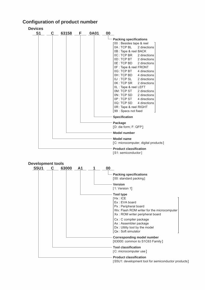
DevicesS1 C 63158 F 0A01
Packing specifications 00 : Besides tape & reel 0A : TCP BL 2 directions 0B : Tape & reel BACK 0C : TCP BR 2 directions 0D : TCP BT 2 directions 0E : TCP BD 2 directions 0F : Tape & reel FRONT 0G : TCP BT 4 directions 0H : TCP BD 4 directions 0J : TCP SL 2 directions 0K : TCP SR 2 directions 0L : Tape & reel LEFT 0M : TCP ST 2 directions 0N : TCP SD 2 directions 0P : TCP ST 4 directions 0Q : TCP SD 4 directions 0R : Tape & reel RIGHT 99 : Specs not fixed
Specification
Package D: die form; F: QFP
Model number
Model name C: microcomputer, digital products
Product classification S1: semiconductor
Development toolsS5U1 C 63000 A1 1
Packing specifications 00: standard packing
Version 1: Version 1
Tool type Hx : ICE Ex : EVA board Px : Peripheral board Wx : Flash ROM writer for the microcomputer Xx : ROM writer peripheral board Cx : C compiler package Ax : Assembler package Dx : Utility tool by the model Qx : Soft simulator
Corresponding model number 63000: common to S1C63 Family
Tool classification C: microcomputer use
Product classification S5U1: development tool for semiconductor products
00
00
Configuration of product number
S1C63406/408 TECHNICAL MANUAL EPSON i
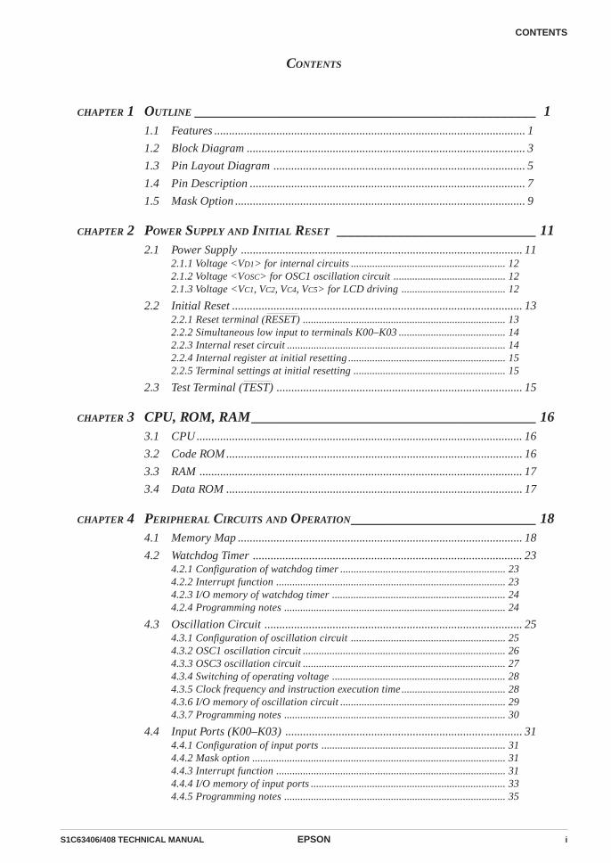
CONTENTS
CONTENTS
CHAPTER 1 OUTLINE ________________________________________________ 11.1 Features ......................................................................................................... 1
1.2 Block Diagram .............................................................................................. 3
1.3 Pin Layout Diagram ..................................................................................... 5
1.4 Pin Description ............................................................................................. 7
1.5 Mask Option .................................................................................................. 9
CHAPTER 2 POWER SUPPLY AND INITIAL RESET ____________________________ 112.1 Power Supply ............................................................................................... 11
2.1.1 Voltage <VD1> for internal circuits .......................................................... 122.1.2 Voltage <VOSC> for OSC1 oscillation circuit .......................................... 122.1.3 Voltage <VC1, VC2, VC4, VC5> for LCD driving ....................................... 12
2.2 Initial Reset .................................................................................................. 132.2.1 Reset terminal (RESET) ............................................................................ 132.2.2 Simultaneous low input to terminals K00–K03 ........................................ 142.2.3 Internal reset circuit .................................................................................. 142.2.4 Internal register at initial resetting ........................................................... 152.2.5 Terminal settings at initial resetting ......................................................... 15
2.3 Test Terminal (TEST) ................................................................................... 15
CHAPTER 3 CPU, ROM, RAM ________________________________________ 163.1 CPU .............................................................................................................. 16
3.2 Code ROM .................................................................................................... 16
3.3 RAM ............................................................................................................. 17
3.4 Data ROM .................................................................................................... 17
CHAPTER 4 PERIPHERAL CIRCUITS AND OPERATION__________________________ 184.1 Memory Map ................................................................................................ 18
4.2 Watchdog Timer ........................................................................................... 234.2.1 Configuration of watchdog timer .............................................................. 234.2.2 Interrupt function ...................................................................................... 234.2.3 I/O memory of watchdog timer ................................................................. 244.2.4 Programming notes ................................................................................... 24
4.3 Oscillation Circuit ....................................................................................... 254.3.1 Configuration of oscillation circuit .......................................................... 254.3.2 OSC1 oscillation circuit ............................................................................ 264.3.3 OSC3 oscillation circuit ............................................................................ 274.3.4 Switching of operating voltage ................................................................. 284.3.5 Clock frequency and instruction execution time ....................................... 284.3.6 I/O memory of oscillation circuit .............................................................. 294.3.7 Programming notes ................................................................................... 30
4.4 Input Ports (K00–K03) ................................................................................ 314.4.1 Configuration of input ports ..................................................................... 314.4.2 Mask option ............................................................................................... 314.4.3 Interrupt function ...................................................................................... 314.4.4 I/O memory of input ports ......................................................................... 334.4.5 Programming notes ................................................................................... 35
ii EPSON S1C63406/408 TECHNICAL MANUAL
CONTENTS
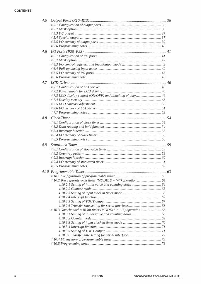
4.5 Output Ports (R10–R13) .............................................................................. 364.5.1 Configuration of output ports ................................................................... 364.5.2 Mask option ............................................................................................... 364.5.3 DC output .................................................................................................. 374.5.4 Special output ............................................................................................ 374.5.5 I/O memory of output ports ....................................................................... 394.5.6 Programming notes ................................................................................... 40
4.6 I/O Ports (P20–P23) .................................................................................... 414.6.1 Configuration of I/O ports ........................................................................ 414.6.2 Mask option ............................................................................................... 424.6.3 I/O control registers and input/output mode ............................................ 424.6.4 Pull-up during input mode ........................................................................ 424.6.5 I/O memory of I/O ports ............................................................................ 434.6.6 Programming note ..................................................................................... 45
4.7 LCD Driver .................................................................................................. 464.7.1 Configuration of LCD driver .................................................................... 464.7.2 Power supply for LCD driving .................................................................. 464.7.3 LCD display control (ON/OFF) and switching of duty ............................ 464.7.4 Display memory ......................................................................................... 484.7.5 LCD contrast adjustment .......................................................................... 504.7.6 I/O memory of LCD driver ........................................................................ 514.7.7 Programming notes ................................................................................... 53
4.8 Clock Timer .................................................................................................. 544.8.1 Configuration of clock timer ..................................................................... 544.8.2 Data reading and hold function ................................................................ 544.8.3 Interrupt function ...................................................................................... 554.8.4 I/O memory of clock timer ........................................................................ 564.8.5 Programming notes ................................................................................... 58
4.9 Stopwatch Timer ........................................................................................... 594.9.1 Configuration of stopwatch timer ............................................................. 594.9.2 Count-up pattern ....................................................................................... 594.9.3 Interrupt function ...................................................................................... 604.9.4 I/O memory of stopwatch timer ................................................................ 614.9.5 Programming notes ................................................................................... 62
4.10 Programmable Timer ................................................................................... 634.10.1 Configuration of programmable timer .................................................... 634.10.2 Tow separate 8-bit timer (MODE16 = "0") operation ........................... 64
4.10.2.1 Setting of initial value and counting down ................................. 644.10.2.2 Counter mode .............................................................................. 654.10.2.3 Setting of input clock in timer mode ........................................... 664.10.2.4 Interrupt function ........................................................................ 674.10.2.5 Setting of TOUT output ............................................................... 674.10.2.6 Transfer rate setting for serial interface ..................................... 68
4.10.3 One channel × 16-bit timer (MODE16 = "1") operation ...................... 684.10.3.1 Setting of initial value and counting down ................................. 684.10.3.2 Counter mode .............................................................................. 694.10.3.3 Setting of input clock in timer mode ........................................... 704.10.3.4 Interrupt function ........................................................................ 714.10.3.5 Setting of TOUT output ............................................................... 714.10.3.6 Transfer rate setting for serial interface ..................................... 72
4.10.4 I/O memory of programmable timer ....................................................... 734.10.5 Programming notes ................................................................................. 78
S1C63406/408 TECHNICAL MANUAL EPSON iii
CONTENTS
4.11 Serial Interface ............................................................................................ 794.11.1 Configuration of serial interface ............................................................ 794.11.2 Mask option ............................................................................................. 804.11.3 Transfer modes ........................................................................................ 804.11.4 Clock source ............................................................................................ 824.11.5 Transmit-receive control ......................................................................... 834.11.6 Operation of clock synchronous transfer ................................................ 844.11.7 Operation of asynchronous transfer ....................................................... 884.11.8 Interrupt function .................................................................................... 924.11.9 I/O memory of serial interface ................................................................ 944.11.10 Programming notes .............................................................................. 100
4.12 SVD (Supply Voltage Detection) Circuit ..................................................... 1014.12.1 Configuration of SVD circuit ................................................................. 1014.12.2 SVD operation ........................................................................................ 1014.12.3 I/O memory of SVD circuit ..................................................................... 1024.12.4 Programming notes ................................................................................ 102
4.13 Heavy Load Protection Function ................................................................ 1034.13.1 Outline of heavy load protection function ............................................. 1034.13.2 I/O memory of heavy load protection function ...................................... 1034.13.3 Programming note .................................................................................. 103
4.14 Interrupt and HALT/SLEEP ....................................................................... 1044.14.1 Interrupt factor ....................................................................................... 1064.14.2 Interrupt mask ........................................................................................ 1074.14.3 Interrupt vector ...................................................................................... 1074.14.4 I/O memory of interrupt ......................................................................... 1084.14.5 Programming notes ................................................................................ 109
CHAPTER 5 SUMMARY OF NOTES ______________________________________ 1105.1 Notes for Low Current Consumption .......................................................... 110
5.2 Summary of Notes by Function ................................................................... 111
5.3 Notes on Mounting ...................................................................................... 115
CHAPTER 6 BASIC EXTERNAL WIRING DIAGRAM ___________________________ 117
CHAPTER 7 ELECTRICAL CHARACTERISTICS _______________________________ 1187.1 Absolute Maximum Rating.......................................................................... 118
7.2 Recommended Operating Conditions ......................................................... 118
7.3 DC Characteristics ..................................................................................... 119
7.4 Analog Circuit Characteristics and Power Current Consumption ............ 120
7.5 Oscillation Characteristics ......................................................................... 123
7.6 Serial Interface AC Characteristics ........................................................... 126
7.7 Timing Chart ............................................................................................... 127
CHAPTER 8 PACKAGE _______________________________________________ 1288.1 Plastic Package ........................................................................................... 128
8.2 Ceramic Package for Test Samples ............................................................. 129
iv EPSON S1C63406/408 TECHNICAL MANUAL
CONTENTS
CHAPTER 9 PAD LAYOUT ____________________________________________ 1309.1 Diagram of Pad Layout ............................................................................... 130
9.2 Pad Coordinates .......................................................................................... 132
APPENDIX S5U1C63000P MANUAL (PERIPHERAL CIRCUIT BOARD FOR S1C63406/408) __ 134A.1 Names and Functions of Each Part ............................................................ 134
A.2 Connecting to the Target System ................................................................ 137
A.3 Usage Precautions ...................................................................................... 139A.3.1 Operational precautions .......................................................................... 139A.3.2 Differences with the actual IC ................................................................. 139
S1C63406/408 TECHNICAL MANUAL EPSON 1
CHAPTER 1: OUTLINE
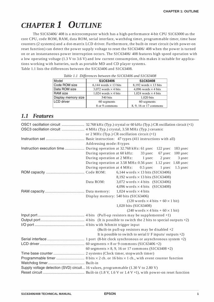
CHAPTER 1 OUTLINEThe S1C63406/408 is a microcomputer which has a high-performance 4-bit CPU S1C63000 as the
core CPU, code ROM, RAM, data ROM, serial interface, watchdog timer, programmable timer, time basecounters (2 systems) and a dot-matrix LCD driver. Furthermore, the built-in reset circuit (with power-onreset function) can detect the power supply voltage to reset the S1C63406/408 when the power is turnedon or an instantaneous power interruption occurs. The S1C63406/408 features high speed operation witha low operating voltage (1.3 V to 3.6 V) and low current consumption, this makes it suitable for applica-tions working with batteries, such as portable MD and CD player systems.Table 1.1 lists the differences between the S1C63406 and S1C63408.
Table 1.1 Differences between the S1C63406 and S1C63408ModelCode ROM sizeData ROM sizeRAM sizeDisplay memory sizeLCD driver
S1C634066,144 words × 13 bits3,072 words × 4 bits1,024 words × 4 bits
540 bits60 segments
8 or 9 commons
S1C634088,192 words × 13 bits4,096 words × 4 bits1,024 words × 4 bits
1,020 bits60 segments
8, 9, 16 or 17 commons
1.1 FeaturesOSC1 oscillation circuit ...................... 32.768 kHz (Typ.) crystal or 60 kHz (Typ.) CR oscillation circuit (∗1)OSC3 oscillation circuit ...................... 4 MHz (Typ.) crystal, 3.58 MHz (Typ.) ceramic
or 2 MHz (Typ.) CR oscillation circuit (∗1)Instruction set ..................................... Basic instruction: 47 types (411 instructions with all)
Addressing mode: 8 typesInstruction execution time ................... During operation at 32.768 kHz: 61 µsec 122 µsec 183 µsec
During operation at 60 kHz: 33 µsec 67 µsec 100 µsecDuring operation at 2 MHz: 1 µsec 2 µsec 3 µsecDuring operation at 3.58 MHz: 0.56 µsec 1.12 µsec 1.68 µsecDuring operation at 4 MHz: 0.5 µsec 1 µsec 1.5 µsec
ROM capacity ..................................... Code ROM: 6,144 words × 13 bits (S1C63406)8,192 words × 13 bits (S1C63408)
Data ROM: 3,072 words × 4 bits (S1C63406)4,096 words × 4 bits (S1C63408)
RAM capacity ...................................... Data memory: 1,024 words × 4 bitsDisplay memory: 540 bits (S1C63406)
(120 words × 4 bits + 60 × 1 bit)1,020 bits (S1C63408)
(240 words × 4 bits + 60 × 1 bit)Input port ............................................. 4 bits (Pull-up resistors may be supplemented ∗1)Output port .......................................... 4 bits (It is possible to switch the 2 bits to special outputs ∗2)I/O port ................................................ 4 bits with Schmitt trigger input
(Built-in pull-up resistors may be disabled ∗2It is possible to switch to serial I/F inputs/outputs ∗2)
Serial interface .................................... 1 port (8-bit clock synchronous or asynchronous system ∗2)LCD driver ........................................... 60 segments × 8 or 9 commons (S1C63406 ∗2)
60 segments × 8, 9, 16 or 17 commons (S1C63408 ∗2)Time base counter .............................. 2 systems (Clock timer, stopwatch timer)Programmable timer ........................... 8 bits × 2 ch. or 16 bits × 1 ch., with event counter functionWatchdog timer ................................... Built-inSupply voltage detection (SVD) circuit ... 16 values, programmable (1.30 V to 2.80 V)Reset circuit ........................................ Built-in (1.8 V, 1.6 V or 1.4 V ∗1), with power-on reset function

2 EPSON S1C63406/408 TECHNICAL MANUAL
CHAPTER 1: OUTLINE
External interrupt ................................ Input port interrupt: 4 systemsInternal interrupt ................................. Clock timer interrupt: 4 systems
Stopwatch timer interrupt: 2 systemsProgrammable timer interrupt: 2 systemsSerial interface interrupt: 3 systems
Power supply voltage .......................... 1.3 V to 3.6 V(Min. 1.4 V when 700 kHz (Max.) OSC3 CR oscillator is used)(Min. 1.6 V when 2.2 MHz (Max.) OSC3 CR oscillator is used)(Min. 1.8 V when 4.2 MHz (Max.) OSC3 oscillator is used)
Operating temperature range ............. -40°C to 85°CCurrent consumption .......................... Low-power operation (∗ 3):
During SLEEP 1.2 µA (Typ.) During HALT (32 kHz cryctal oscillation)
3.6 V (LCD OFF) 1.3 µA (Typ.)3.6 V (LCD ON, VC1 standard) 3.0 µA (Typ.)3.6 V (LCD ON, VC2 standard) 2.5 µA (Typ.)
During operation (32 kHz cryctal oscillation)3.6 V (LCD OFF) 3.0 µA (Typ.)
During HALT (60 kHz CR oscillation)3.6 V (LCD OFF) 3.5 µA (Typ.)3.6 V (LCD ON, VC1 standard) 6.2 µA (Typ.)3.6 V (LCD ON, VC2 standard) 4.6 µA (Typ.)
During operation (60 kHz CR oscillation)3.6 V (LCD OFF) 7.0 µA (Typ.)
High-speed operation: During operation (500 kHz CR oscillation)
3.6 V (LCD OFF) 90 µA (Typ.) During operation (1 MHz CR oscillation)
3.6 V (LCD OFF) 200 µA (Typ.) During operation (2 MHz CR oscillation)
3.6 V (LCD OFF) 350 µA (Typ.) During operation (3.58 MHz ceramic oscillation)
3.6 V (LCD OFF) 500 µA (Typ.) During operation (4 MHz crystal oscillation)
3.6 V (LCD OFF) 550 µA (Typ.)Package .............................................. TQFP15-128pin (plastic) or chip (S1C63406)
QFP15-128pin (plastic) or chip (S1C63408)∗ 1: Can be selected with mask option ∗ 2: Can be selected with software∗ 3: Current consumption when the reset circuit option is not selected (Reset
circuit current will be added when the reset circuit option is selected.)
S1C63406/408 TECHNICAL MANUAL EPSON 3
CHAPTER 1: OUTLINE
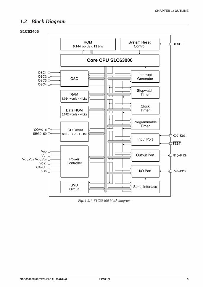
1.2 Block Diagram
S1C63406
OSC1OSC2OSC3OSC4
COM0–8SEG0–59
VDD
VD1
VC1, VC2, VC4, VC5
VOSC
CA–CFVSS
K00–K03
TEST
RESET
P20–P23
R10–R13
Core CPU S1C63000
ROM6,144 words × 13 bits
System ResetControl
InterruptGeneratorOSC
RAM1,024 words × 4 bits
Data ROM3,072 words × 4 bits
LCD Driver60 SEG × 9 COM
PowerController
SVDCircuit
StopwatchTimer
ClockTimer
ProgrammableTimer
Output Port
Input Port
I/O Port
Serial Interface
Fig. 1.2.1 S1C63406 block diagram

4 EPSON S1C63406/408 TECHNICAL MANUAL
CHAPTER 1: OUTLINE
S1C63408
OSC1OSC2OSC3OSC4
COM0–16SEG0–59
VDD
VD1
VC1, VC2, VC4, VC5
VOSC
CA–CFVSS
K00–K03
TEST
RESET
P20–P23
R10–R13
Core CPU S1C63000
ROM8,192 words × 13 bits
System ResetControl
InterruptGeneratorOSC
RAM1,024 words × 4 bits
Data ROM4,096 words × 4 bits
LCD Driver60 SEG × 17 COM
PowerController
SVDCircuit
StopwatchTimer
ClockTimer
ProgrammableTimer
Output Port
Input Port
I/O Port
Serial Interface
Fig. 1.2.2 S1C63408 block diagram
S1C63406/408 TECHNICAL MANUAL EPSON 5
CHAPTER 1: OUTLINE
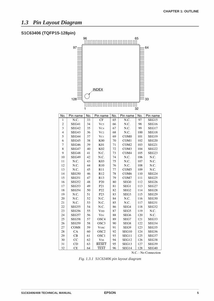
1.3 Pin Layout Diagram
S1C63406 (TQFP15-128pin)6596
33
64
INDEX
321
128
97
No.1234567891011121314151617181920212223242526272829303132
No.3334353637383940414243444546474849505152535455565758596061626364
No.6566676869707172737475767778798081828384858687888990919293949596
No.979899100101102103104105106107108109110111112113114115116117118119120121122123124125126127128
Pin nameN.C.
SEG41SEG42SEG43SEG44SEG45SEG46SEG47SEG48SEG49N.C.N.C.N.C.
SEG50SEG51SEG52SEG53SEG54N.C.N.C.N.C.
SEG55SEG56SEG57SEG58SEG59COM8
CACBCCCDCE
Pin nameCFVC5
VC4
VC2
VC1
K00K01K02N.C.N.C.K03R10R11R12R13P20P21P22P23N.C.N.C.N.C.VDD
VD1
OSC4OSC3VOSC
OSC2OSC1VSS
RESETTEST
Pin nameN.C.N.C.N.C.N.C.
COM0COM1COM2COM3COM4N.C.N.C.N.C.
COM5COM6COM7SEG0SEG1SEG2SEG3N.C.N.C.SEG4SEG5SEG6SEG7SEG8SEG9SEG10SEG11SEG12SEG13SEG14
Pin nameSEG15SEG16SEG17SEG18SEG19SEG20SEG21SEG22SEG23N.C.N.C.N.C.N.C.
SEG24SEG25SEG26SEG27SEG28SEG29SEG30SEG31SEG32N.C.N.C.
SEG33SEG34SEG35SEG36SEG37SEG38SEG39SEG40
N.C. : No Connection
Fig. 1.3.1 S1C63406 pin layout diagram

6 EPSON S1C63406/408 TECHNICAL MANUAL
CHAPTER 1: OUTLINE
S1C63408 (QFP15-128pin)6596
33
64
INDEX
321
128
97
No.1234567891011121314151617181920212223242526272829303132
No.3334353637383940414243444546474849505152535455565758596061626364
No.6566676869707172737475767778798081828384858687888990919293949596
No.979899100101102103104105106107108109110111112113114115116117118119120121122123124125126127128
Pin nameN.C.N.C.N.C.
SEG46SEG47SEG48SEG49SEG50SEG51SEG52SEG53SEG54SEG55SEG56SEG57SEG58SEG59COM8COM9COM10COM11COM12COM13COM14COM15COM16
CACBCCCDN.C.N.C.
Pin nameN.C.N.C.CECFVC5
VC4
VC2
VC1
K00K01K02K03R10R11R12R13P20P21P22P23VDD
VD1
OSC4OSC3VOSC
OSC2OSC1VSS
RESETTESTN.C.N.C.
Pin nameN.C.N.C.
COM0COM1COM2N.C.
COM3COM4COM5COM6COM7SEG0SEG1SEG2SEG3SEG4SEG5SEG6SEG7SEG8SEG9SEG10SEG11SEG12SEG13SEG14SEG15SEG16SEG17N.C.
SEG18N.C.
Pin nameN.C.N.C.
SEG19N.C.
SEG20SEG21SEG22SEG23SEG24SEG25SEG26SEG27SEG28SEG29SEG30SEG31SEG32SEG33SEG34SEG35SEG36SEG37SEG38SEG39SEG40SEG41SEG42SEG43SEG44SEG45N.C.N.C.
N.C. : No Connection
Fig. 1.3.2 S1C63408 pin layout diagram

S1C63406/408 TECHNICAL MANUAL EPSON 7
CHAPTER 1: OUTLINE
1.4 Pin Description
S1C63406Table 1.4.1 S1C63406 pin description
Pin name
VDD
VSS
VD1
VOSC
VC1, VC2, VC4, VC5
CA–CF
OSC1
OSC2
OSC3
OSC4
K00–K02
K03
R10, R11
R12
R13
P20
P21
P22
P23
COM0–COM8
SEG0–SEG59
RESET
TEST
Pin No.
55
62
56
59
37, 36, 35, 34
28–33
61
60
58
57
38–40
43
44, 45
46
47
48
49
50
51
69–73, 77–79, 27
80–83, 86–105,
110–118, 121–128,
2–10, 14–18, 22–26
63
64
Function
Power (+) supply pin
Power (–) supply pin
Internal logic system regulated voltage output pin
Oscillation system regulated voltage output pin
LCD system power supply pins (1/4 bias)
LCD system boosting/reducing capacitor connecting pins
Crystal or CR oscillation input pin (selected by mask option)
Crystal or CR oscillation output pin (selected by mask option)
Crystal, ceramic or CR oscillation input pin (selected by mask option)
Crystal, ceramic or CR oscillation output pin (selected by mask option)
Input port pins
Input port pin or EVIN signal input pin (selected by software)
Output port pins
Output port pin or TOUT signal output pin (selected by software)
Output port pin or FOUT signal output pin (selected by software)
I/O port pins or serial I/F data input pin (selected by software)
I/O port pins or serial I/F data output pin (selected by software)
I/O port pins or serial I/F clock input/output pin (selected by software)
I/O port pins or serial I/F ready signal output pin (selected by software)
LCD common output pin
LCD segment output pin
Initial reset input pin
Testing input pin
In/Out
–
–
–
–
–
–
I
O
I
O
I
I
O
O
O
I/O
I/O
I/O
I/O
O
O
I
I
8 EPSON S1C63406/408 TECHNICAL MANUAL
CHAPTER 1: OUTLINE
S1C63408Table 1.4.2 S1C63408 pin description
Pin name
VDD
VSS
VD1
VOSC
VC1, VC2, VC4, VC5
CA–CF
OSC1
OSC2
OSC3
OSC4
K00–K02
K03
R10, R11
R12
R13
P20
P21
P22
P23
COM0–COM16
SEG0–SEG59
RESET
TEST
Pin No.
53
60
54
57
40, 39, 38, 37
27–30, 35, 36
59
58
56
55
41–43
44
45, 46
47
48
49
50
51
52
67–69, 71–75, 18–26
76–93, 95, 99,
101–126, 4–17
61
62
Function
Power (+) supply pin
Power (–) supply pin
Internal logic system regulated voltage output pin
Oscillation system regulated voltage output pin
LCD system power supply pins (1/4 bias)
LCD system boosting/reducing capacitor connecting pins
Crystal or CR oscillation input pin (selected by mask option)
Crystal or CR oscillation output pin (selected by mask option)
Crystal, ceramic or CR oscillation input pin (selected by mask option)
Crystal, ceramic or CR oscillation output pin (selected by mask option)
Input port pins
Input port pin or EVIN signal input pin (selected by software)
Output port pins
Output port pin or TOUT signal output pin (selected by software)
Output port pin or FOUT signal output pin (selected by software)
I/O port pins or serial I/F data input pin (selected by software)
I/O port pins or serial I/F data output pin (selected by software)
I/O port pins or serial I/F clock input/output pin (selected by software)
I/O port pins or serial I/F ready signal output pin (selected by software)
LCD common output pin
LCD segment output pin
Initial reset input pin
Testing input pin
In/Out
–
–
–
–
–
–
I
O
I
O
I
I
O
O
O
I/O
I/O
I/O
I/O
O
O
I
I

S1C63406/408 TECHNICAL MANUAL EPSON 9
CHAPTER 1: OUTLINE
1.5 Mask OptionMask options shown below are provided for the S1C63406/408. Several hardware specifications areprepared in each mask option, and one of them can be selected according to the application. The functionoption generator winfog, that has been prepared as the development software tool of S1C63406/408, isused for this selection. Mask pattern of the IC is finally generated based on the data created by thewinfog. Refer to the "S5U1C63000A Manual" for the winfog.
<Mask Option List>The following is the option list for the S1C63406/408.Multiple selections are available in each option item as indicated in the option list. Using "4 PeripheralCircuits and Operation" as reference, select the spcifications that meet the target system and check theappropriate box. Be sure to record the spcifications for unused functions too, according to theinstructions provied.
1. OSC1 SYSTEM CLOCK 1. Crystal (32.768 kHz) 2. CR (60 kHz)
2. OSC3 SYSTEM CLOCK 1. CR 2. Ceramic (3.58 MHz) 3. Crystal (4 MHz)
3. RESET CIRCUIT 1. Use (1.8 V) 2. Use (1.6 V) 3. Use (1.4 V) 4. Not Use
4. MULTIPLE KEY ENTRY RESET COMBINATION 1. Not Use 2. Use (K00, K01, K02, K03) 3. Use (K00, K01, K02) 4. Use (K00, K01)
5. MULTIPLE KEY ENTRY RESET TIME AUTHORIZE 1. Not Use 2. Use
6. INPUT PORT PULL UP RESISTOR• K00 1. With Resistor 2. Gate Direct• K01 1. With Resistor 2. Gate Direct• K02 1. With Resistor 2. Gate Direct• K03 1. With Resistor 2. Gate Direct
7. OUTPUT PORT OUTPUT SPECIFICATION• R10 1. Complementary 2. Nch-OpenDrain• R11 1. Complementary 2. Nch-OpenDrain• R12 1. Complementary 2. Nch-OpenDrain• R13 1. Complementary 2. Nch-OpenDrain
8. I/O PORT OUTPUT SPECIFICATION• P20 1. Complementary 2. Nch-OpenDrain• P21 1. Complementary 2. Nch-OpenDrain• P22 1. Complementary 2. Nch-OpenDrain• P23 1. Complementary 2. Nch-OpenDrain

10 EPSON S1C63406/408 TECHNICAL MANUAL
CHAPTER 1: OUTLINE
<Outline of Mask Option>
(1) OSC1 oscillation circuit
Crystal or CR oscillation can be selected as the OSC1 oscillation circuit.Refer to Section 4.3.2, "OSC1 oscillation circuit", for details.
(2) OSC3 oscillation circuit
Crystal, ceramic or CR oscillation can be selected as the OSC3 oscillation circuit.Select item 3 when using a crystal oscillator or item 2 when using a ceramic oscillator. The frequenciesin parentheses are recommended typical values. Refer to Section 4.3.3, "OSC3 oscillation circuit", fordetails.
(3) Internal reset circuit
This mask option selects whether the internal reset circuit is used or not. Select a minimum supplyvoltage according to the oscillation frequency when this circuit is used.Refer to Section 2.2.3, "Internal reset circuit", for details.
(4) External reset by simultaneous LOW input to the I/O port (K00–K03)
This function resets the IC when several keys are pressed simultaneously. The mask option is used toselect whether this function is used or not. Further when the function is used, a combination of theinput terminals (K00–K03), which are connected to the keys to be pressed simultaneously, can beselected. Refer to Section 2.2.2, "Simultaneous low input to terminals K00–K03", for details.
(5) Time authorize circuit for the simultaneous LOW input reset function
When using the external reset function (shown in 4 above), using the time authorize circuit or not canbe selected by mask option. The reset function works only when the input time of simultaneous LOWis more than the rule time if the time authorize circuit is being used.Refer to Section 2.2.2, "Simultaneous low input to terminals K00–K03", for details.
(6) Input port pull-up resistor
The mask option is used to select whether the pull-up resistor is supplemented to the input ports ornot. It is possible to select for each bit of the input ports.Refer to Section 4.4.2, "Mask option", for details.
(7) Output specification of the output port
Either complementary output or N-channel open drain output can be selected as the output specifica-tion for the output ports. The selection is done in 1-bit units.Refer to Section 4.5.2, "Mask option", for details.
(8) Output specification of the I/O ports
For the output specification when the I/O ports are in the output mode, either complementary outputor N-channel open drain output can be selected in 1-bit units.Refer to Section 4.6.2, "Mask option", for details.
S1C63406/408 TECHNICAL MANUAL EPSON 11
CHAPTER 2: POWER SUPPLY AND INITIAL RESET
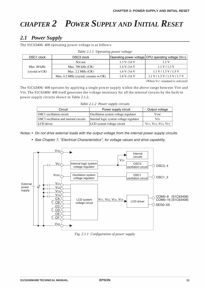
CHAPTER 2 POWER SUPPLY AND INITIAL RESET
2.1 Power SupplyThe S1C63406/408 operating power voltage is as follows:
Table 2.1.1 Operating power voltage
OSC1 clock
Max. 80 kHz
(crystal or CR)
OSC3 clock
Not use
Max. 700 kHz (CR)
Max. 2.2 MHz (CR)
Max. 4.2 MHz (crystal, ceramic or CR)
Operating power voltage
1.3 V–3.6 V
1.4 V–3.6 V
1.6 V–3.6 V
1.8 V–3.6 V
CPU operating voltage (VD1)
1.1 V
1.1 V / 1.3 V
1.1 V / 1.3 V / 1.5 V
1.1 V / 1.3 V / 1.5 V / 1.7 V
(When VC1 standard is selected)
The S1C63406/408 operates by applying a single power supply within the above range between VDD andVSS. The S1C63406/408 itself generates the voltage necessary for all the internal circuits by the built-inpower supply circuits shown in Table 2.1.2.
Table 2.1.2 Power supply circuits
Circuit
OSC1 oscillation circuit
OSC3 oscillation and internal circuits
LCD driver
Power supply circuit
Oscillation system voltage regulator
Internal logic system voltage regulator
LCD system voltage circuit
Output voltage
VOSC
VD1
VC1, VC2, VC4, VC5
Notes: • Do not drive external loads with the output voltage from the internal power supply circuits.
• See Chapter 7, "Electrical Characteristics", for voltage values and drive capability.
COM0–8 (S1C63406)COM0–16 (S1C63408)
SEG0–59
Externalpowersupply
Internalcircuits
OSC3oscillation circuit
LCD systemvoltage circuit
Internal logic systemvoltage regulator
VDD
VV
OSC3, 4D1
D1
VVVVCACBCCCDCECF
C1
C2
C4
C5
LCD driver
VSS
+
VC1, VC2, VC4, VC5
OSC1oscillation circuit
VOSCOSC1, 2
Oscillation systemvoltage regulator
Fig. 2.1.1 Configuration of power supply

12 EPSON S1C63406/408 TECHNICAL MANUAL
CHAPTER 2: POWER SUPPLY AND INITIAL RESET
2.1.1 Voltage <VD1> for internal circuitsVD1 is the voltage for the OSC3 oscillation circuit and the internal logic circuits, and is generated by theinternal logic system voltage regulator.The S1C63406/408 is designed with twin clock specification; it has two types of oscillation circuits OSC1and OSC3 built-in. Use OSC1 clock for normal operation, and switch it to OSC3 by the software whenhigh-speed operation is necessary. When switching the clock, the operating voltage VD1 must be switchedby the software to stabilize the operation of the oscillation circuit and internal circuits.The internal logic system voltage regulator can output the following four types of VD1 voltage. It shouldbe set at the value according to the oscillation circuit and oscillation frequency by the software.
VD1 = 1.1 V for low-power operation (when OSC3 oscillation is OFF)VD1 = 1.3 V for high-speed operation (when Max. 700 kHz OSC3 CR oscillation is ON)VD1 = 1.5 V for high-speed operation (when Max. 2.2 MHz OSC3 CR oscillation is ON)VD1 = 1.7 V for high-speed operation (when Max. 4.2 MHz OSC3 crystal/ceramic/CR oscillation is ON)
Refer to Section 4.3, "Oscillation Circuit", for the VD1 switching procedure.
2.1.2 Voltage <VOSC> for OSC1 oscillation circuitVOSC is the voltage for the OSC1 oscillation circuit and is generated by the oscillation system voltageregulator for stabilizing the oscillation.
2.1.3 Voltage <VC1, VC2, VC4, VC5> for LCD drivingVC1, VC2, VC4 and VC5 are the LCD drive voltages generated by the LCD system voltage circuit. Thesefour output voltages can only be supplied to the externally expanded LCD driver.The LCD system voltage circuit generates VC1 or VC2 with the voltage regulator built-in, and generatesthree other voltages by boosting or reducing the voltage of VC1 or VC2. Table 2.1.3.1 shows the VC1, VC2,VC4 and VC5 voltage values and boost/reduce status.
Table 2.1.3.1 LCD drive voltage when generated internally
LCD drive voltage
VC1 (0.975–1.2 V)
VC2 (1.950–2.4 V)
VC4 (2.925–3.6 V)
VC5 (3.900–4.8 V)
VDD = 1.3–3.6 V
VC1 (standard)
2 × VC1
3 × VC1
4 × VC1
VDD = 2.5–3.6 V
1/2 × VC2
VC2 (standard)
3/2 × VC2
2 × VC2
Note: The LCD drive voltage can be adjusted by the software (see Section 4.7.5). Values in the abovetable are typical values.
Either the VC1 or VC2 used for the standard is selected according to the supply voltage by the software.The VC2 standard improves the display quality and reduces current consumption, however, the powersupply voltage VDD must be 2.5 V or more.Refer to Section 4.7, "LCD Driver", for control of the LCD drive voltage.

S1C63406/408 TECHNICAL MANUAL EPSON 13
CHAPTER 2: POWER SUPPLY AND INITIAL RESET
2.2 Initial ResetTo initialize the S1C63406/408 circuits, initial reset must be executed. There are three ways of doing this.
(1) External initial reset by the RESET terminal(2) External initial reset by simultaneous low input to terminals K00–K03 (mask option)(3) Internal initial reset by the reset circuit (mask option)
When the power is turned on, be sure to initialize using the reset function. Figure 2.2.1 shows the con-figuration of the initial reset circuit.
RESET
K00
K01
K02
K03
OSC2OSC1
R Q
S
Internalinitialreset
Divider
VDD
1 kHz
1 Hz16 Hz
VDD
OSC1oscillation
circuit
Noiserejectcircuit
Timeauthorize
circuit
ResetcircuitReset signal
Mask option
Mask option
Mask option
Fig. 2.2.1 Configuration of initial reset circuit
2.2.1 Reset terminal (RESET)Initial reset can be executed externally by setting the reset terminal to a low level (VSS). After that theinitial reset is released by setting the reset terminal to a high level (VDD) and the CPU starts operation.The reset input signal is maintained by the RS latch and becomes the internal initial reset signal. The RSlatch is designed to be released by a 16 Hz signal (high) that is divided by the OSC1 clock. Therefore innormal operation, a maximum of 1024/fOSC1 seconds (32 msec when fOSC1 is 32.768 kHz) is needed untilthe internal initial reset is released after the reset terminal goes to high level. Be sure to maintain a resetinput of 0.1 msec or more.However, when turning the power on, the reset terminal should be set at a low level as in the timingshown in Figure 2.2.1.1.
VDD
RESET
2.0 msec or more
1.3 V
0.5•VDD
0.1•VDD or less (low level)Power on
Fig. 2.2.1.1 Initial reset at power on
The reset terminal should be set to 0.1•VDD or less (low level) until the supply voltage becomes 1.3 V ormore.After that, a level of 0.5•VDD or less should be maintained more than 2.0 msec.
14 EPSON S1C63406/408 TECHNICAL MANUAL
CHAPTER 2: POWER SUPPLY AND INITIAL RESET
2.2.2 Simultaneous low input to terminals K00–K03Another way of executing initial reset externally is to input a low signal simultaneously to the input ports(K00–K03) selected with the mask option.Since this initial reset passes through the noise reject circuit, maintain the specified input terminals at lowlevel for at least 1.5 msec (when the oscillation frequency fOSC1 is 32.768 kHz) during normal operation.The noise reject circuit does not operate immediately after turning the power on until the oscillationcircuit starts oscillating. Therefore, maintain the specified input terminals at low level for at least 1.5 msec(when the oscillation frequency fOSC1 is 32.768 kHz) after oscillation starts.Table 2.2.2.1 shows the combinations of input ports (K00–K03) that can be selected with the mask option.
Table 2.2.2.1 Combinations of input ports
Not use
K00∗K01∗K02∗K03
K00∗K01∗K02
K00∗K01
1
2
3
4
When, for instance, mask option 2 (K00∗K01∗K02∗K03) isselected, initial reset is executed when the signals input to thefour ports K00–K03 are all low at the same time. When 3 or 4is selected, the initial reset is done when a key entry includinga combination of selected ports is made.
Further, the time authorize circuit can be selected with the mask option. The time authorize circuit checksthe input time of the simultaneous low input and performs initial reset if that time is the defined time (1to 2 sec) or more. If using this function, make sure that the specified port terminals do not go low at thesame time during ordinary operation.
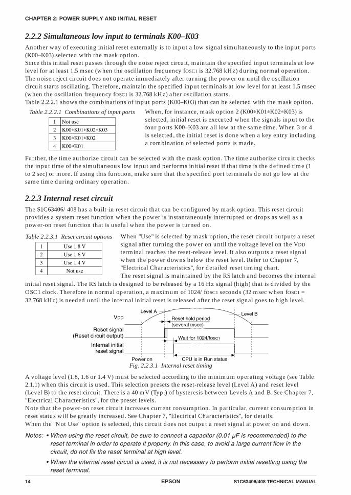
2.2.3 Internal reset circuitThe S1C63406/408 has a built-in reset circuit that can be configured by mask option. This reset circuitprovides a system reset function when the power is instantaneously interrupted or drops as well as apower-on reset function that is useful when the power is turned on.
Table 2.2.3.1 Reset circuit options
Use 1.8 V
Use 1.6 V
Use 1.4 V
Not use
1
2
3
4
When "Use" is selected by mask option, the reset circuit outputs a resetsignal after turning the power on until the voltage level on the VDD
terminal reaches the reset-release level. It also outputs a reset signalwhen the power downs below the reset level. Refer to Chapter 7,"Electrical Characteristics", for detailed reset timing chart.The reset signal is maintained by the RS latch and becomes the internal
initial reset signal. The RS latch is designed to be released by a 16 Hz signal (high) that is divided by theOSC1 clock. Therefore in normal operation, a maximum of 1024/fOSC1 seconds (32 msec when fOSC1 =32.768 kHz) is needed until the internal initial reset is released after the reset signal goes to high level.
VDD
Reset signal(Reset circuit output)
Internal initialreset signal
CPU is in Run status
Level A Level B
Power on
Wait for 1024/fOSC1
Reset hold period(several msec)
Fig. 2.2.3.1 Internal reset timing
A voltage level (1.8, 1.6 or 1.4 V) must be selected according to the minimum operating voltage (see Table2.1.1) when this circuit is used. This selection presets the reset-release level (Level A) and reset level(Level B) to the reset circuit. There is a 40 mV (Typ.) of hysteresis between Levels A and B. See Chapter 7,"Electrical Characteristics", for the preset levels.Note that the power-on reset circuit increases current consumption. In particular, current consumption inreset status will be greatly increased. See Chapter 7, "Electrical Characteristics", for details.When the "Not Use" option is selected, this circuit does not output a reset signal at power on and down.
Notes: • When using the reset circuit, be sure to connect a capacitor (0.01 µF is recommended) to thereset terminal in order to operate it properly. In this case, to avoid a large current flow in thecircuit, do not fix the reset terminal at high level.
• When the internal reset circuit is used, it is not necessary to perform initial resetting using thereset terminal.
S1C63406/408 TECHNICAL MANUAL EPSON 15
CHAPTER 2: POWER SUPPLY AND INITIAL RESET
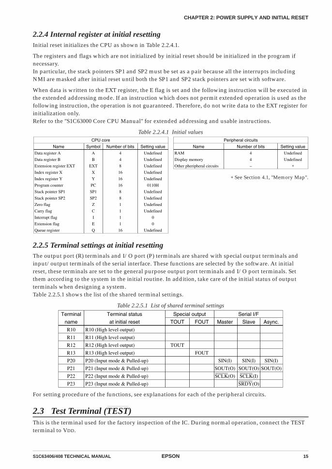
2.2.4 Internal register at initial resettingInitial reset initializes the CPU as shown in Table 2.2.4.1.
The registers and flags which are not initialized by initial reset should be initialized in the program ifnecessary.In particular, the stack pointers SP1 and SP2 must be set as a pair because all the interrupts includingNMI are masked after initial reset until both the SP1 and SP2 stack pointers are set with software.
When data is written to the EXT register, the E flag is set and the following instruction will be executed inthe extended addressing mode. If an instruction which does not permit extended operation is used as thefollowing instruction, the operation is not guaranteed. Therefore, do not write data to the EXT register forinitialization only.Refer to the "S1C63000 Core CPU Manual" for extended addressing and usable instructions.
Table 2.2.4.1 Initial values
Name
Data register A
Data register B
Extension register EXT
Index register X
Index register Y
Program counter
Stack pointer SP1
Stack pointer SP2
Zero flag
Carry flag
Interrupt flag
Extension flag
Queue register
CPU core
Symbol
A
B
EXT
X
Y
PC
SP1
SP2
Z
C
I
E
Q
Number of bits
4
4
8
16
16
16
8
8
1
1
1
1
16
Setting value
Undefined
Undefined
Undefined
Undefined
Undefined
0110H
Undefined
Undefined
Undefined
Undefined
0
0
Undefined
Name
RAM
Display memory
Other pheripheral circuits
Peripheral circuits
Number of bits
4
4
–
Setting value
Undefined
Undefined
∗
∗ See Section 4.1, "Memory Map".
2.2.5 Terminal settings at initial resettingThe output port (R) terminals and I/O port (P) terminals are shared with special output terminals andinput/output terminals of the serial interface. These functions are selected by the software. At initialreset, these terminals are set to the general purpose output port terminals and I/O port terminals. Setthem according to the system in the initial routine. In addition, take care of the initial status of outputterminals when designing a system.Table 2.2.5.1 shows the list of the shared terminal settings.
Table 2.2.5.1 List of shared terminal settings
Terminal
name
R10
R11
R12
R13
P20
P21
P22
P23
Terminal status
at initial reset
R10 (High level output)
R11 (High level output)
R12 (High level output)
R13 (High level output)
P20 (Input mode & Pulled-up)
P21 (Input mode & Pulled-up)
P22 (Input mode & Pulled-up)
P23 (Input mode & Pulled-up)
Special output
TOUT FOUT
TOUT
FOUT
Serial I/F
Master Slave Async.
SIN(I) SIN(I) SIN(I)
SOUT(O) SOUT(O) SOUT(O)
SCLK(O) SCLK(I)
SRDY(O)
For setting procedure of the functions, see explanations for each of the peripheral circuits.
2.3 Test Terminal (TEST)This is the terminal used for the factory inspection of the IC. During normal operation, connect the TESTterminal to VDD.
16 EPSON S1C63406/408 TECHNICAL MANUAL
CHAPTER 3: CPU, ROM, RAM
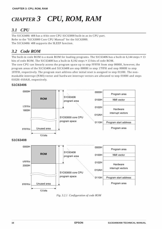
CHAPTER 3 CPU, ROM, RAM3.1 CPUThe S1C63406/408 has a 4-bit core CPU S1C63000 built-in as its CPU part.Refer to the "S1C63000 Core CPU Manual" for the S1C63000.The S1C63406/408 supports the SLEEP function.
3.2 Code ROMThe built-in code ROM is a mask ROM for loading programs. The S1C63406 has a built-in 6,144 steps × 13bits of code ROM. The S1C63408 has a built-in 8,192 steps × 13 bits of code ROM.The core CPU can linearly access the program space up to step FFFFH from step 0000H, however, theprogram areas of the S1C63406 and S1C63408 are step 0000H to step 17FFH and step 0000H to step1FFFH, respectively. The program start address after initial reset is assigned to step 0110H. The non-maskable interrupt (NMI) vector and hardware interrupt vectors are allocated to step 0100H and steps0102H–010AH, respectively.
S1C63406
0000H
17FFH
1800H
FFFFH
0000H
0100H
0102H
010AH
0110H
Program area
NMI vector
Hardware
interrupt vectors
Program start address
Program area
ROM
Unused area
13 bits
S1C63000 core CPU
program space
S1C63406
program area
S1C63408
0000H
1FFFH
2000H
FFFFH
0000H
0100H
0102H
010AH
0110H
Program area
NMI vector
Hardware
interrupt vectors
Program start address
Program area
ROM
Unused area
13 bits
S1C63000 core CPU
program space
S1C63408
program area
Fig. 3.2.1 Configuration of code ROM
S1C63406/408 TECHNICAL MANUAL EPSON 17
CHAPTER 3: CPU, ROM, RAM
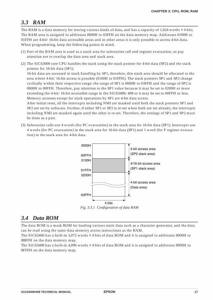
3.3 RAMThe RAM is a data memory for storing various kinds of data, and has a capacity of 1,024 words × 4 bits.The RAM area is assigned to addresses 0000H to 03FFH on the data memory map. Addresses 0100H to01FFH are 4-bit/16-bit data accessible areas and in other areas it is only possible to access 4-bit data.When programming, keep the following points in mind.
(1) Part of the RAM area is used as a stack area for subroutine call and register evacuation, so payattention not to overlap the data area and stack area.
(2) The S1C63000 core CPU handles the stack using the stack pointer for 4-bit data (SP2) and the stackpointer for 16-bit data (SP1).16-bit data are accessed in stack handling by SP1, therefore, this stack area should be allocated to thearea where 4-bit/16-bit access is possible (0100H to 01FFH). The stack pointers SP1 and SP2 changecyclically within their respective range: the range of SP1 is 0000H to 03FFH and the range of SP2 is0000H to 00FFH. Therefore, pay attention to the SP1 value because it may be set to 0200H or moreexceeding the 4-bit/16-bit accessible range in the S1C63406/408 or it may be set to 00FFH or less.Memory accesses except for stack operations by SP1 are 4-bit data access.After initial reset, all the interrupts including NMI are masked until both the stack pointers SP1 andSP2 are set by software. Further, if either SP1 or SP2 is re-set when both are set already, the interruptsincluding NMI are masked again until the other is re-set. Therefore, the settings of SP1 and SP2 mustbe done as a pair.
(3) Subroutine calls use 4 words (for PC evacuation) in the stack area for 16-bit data (SP1). Interrupts use4 words (for PC evacuation) in the stack area for 16-bit data (SP1) and 1 word (for F register evacua-tion) in the stack area for 4-bit data.
0000H
00FFH
0100H
01FFH
0200H
03FFH
4 bits
4-bit access area
(SP2 stack area)
4-bit access area
(Data area)
4/16-bit access area
(SP1 stack area)
Fig. 3.3.1 Configuration of data RAM
3.4 Data ROMThe data ROM is a mask ROM for loading various static data such as a character generator, and the datacan be read using the same data memory access instructions as the RAM.The S1C63406 has a built-in 3,072 words × 4 bits of data ROM and it is assigned to addresses 8000H to8BFFH on the data memory map.The S1C63408 has a built-in 4,096 words × 4 bits of data ROM and it is assigned to addresses 8000H to8FFFH on the data memory map.
18 EPSON S1C63406/408 TECHNICAL MANUAL
CHAPTER 4: PERIPHERAL CIRCUITS AND OPERATION (Memory Map)
CHAPTER 4 PERIPHERAL CIRCUITS AND OPERATIONThe peripheral circuits of S1C63406/408 (timer, I/O, etc.) are interfaced with the CPU in the
memory mapped I/O method. Thus, all the peripheral circuits can be controlled by accessing the I/Omemory on the memory map using the memory operation instructions. The following sections explainthe detailed operation of each peripheral circuit.
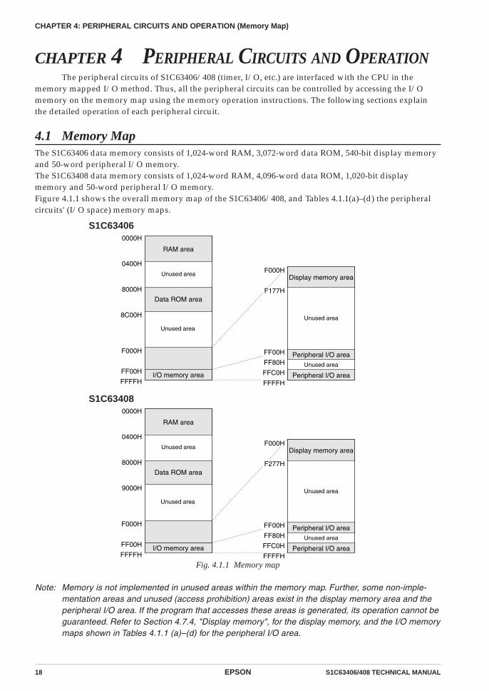
4.1 Memory MapThe S1C63406 data memory consists of 1,024-word RAM, 3,072-word data ROM, 540-bit display memoryand 50-word peripheral I/O memory.The S1C63408 data memory consists of 1,024-word RAM, 4,096-word data ROM, 1,020-bit displaymemory and 50-word peripheral I/O memory.Figure 4.1.1 shows the overall memory map of the S1C63406/408, and Tables 4.1.1(a)–(d) the peripheralcircuits' (I/O space) memory maps.
S1C634060000H
0400H
8000H
8C00H
F000H
FF00H
FFFFH
RAM area
Unused area
Unused area
Data ROM area
I/O memory area
Display memory area
Unused area
Unused area
Peripheral I/O area
Peripheral I/O area
F000H
F177H
FF00H
FF80H
FFC0H
FFFFH
S1C634080000H
0400H
8000H
9000H
F000H
FF00H
FFFFH
RAM area
Unused area
Unused area
Data ROM area
I/O memory area
Display memory area
Unused area
Unused area
Peripheral I/O area
Peripheral I/O area
F000H
F277H
FF00H
FF80H
FFC0H
FFFFHFig. 4.1.1 Memory map
Note: Memory is not implemented in unused areas within the memory map. Further, some non-imple-mentation areas and unused (access prohibition) areas exist in the display memory area and theperipheral I/O area. If the program that accesses these areas is generated, its operation cannot beguaranteed. Refer to Section 4.7.4, "Display memory", for the display memory, and the I/O memorymaps shown in Tables 4.1.1 (a)–(d) for the peripheral I/O area.

S1C63406/408 TECHNICAL MANUAL EPSON 19
CHAPTER 4: PERIPHERAL CIRCUITS AND OPERATION (Memory Map)
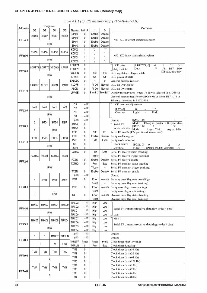
Table 4.1.1 (a) I/O memory map (FF00H–FF4AH)
Remarks
∗ 1 Initial value at initial reset ∗ 2 Not set in the circuit ∗ 3 Constantly "0" when being read
Address CommentD3 D2
Register
D1 D0 Name Init ∗ 1 1 0
FF06HFOUTE FOFQ2 FOFQ1 FOFQ0
R/W
FOUTEFOFQ2FOFQ1FOFQ0
0000
Enable Disable FOUT enable
FOUT
frequency
selection
FF07HHLMOD 0 WDEN WDRST
R/W R R/W W
HLMOD 0 ∗ 3
WDENWDRST∗ 3
0 – ∗ 2
1Reset
On
EnableReset
Off
DisableInvalid
Heavy load protection
Unused
Watchdog timer enable
Watchdog timer reset (writing)
FF00HCLKCHG OSCC VDC1 VDC0
R/W
CLKCHGOSCCVDC1VDC0
0000
OSC3On
OSC1Off
CPU clock switch
OSC3 oscillation On/Off
CPU operating
voltage switch
FF42HK03 K02 K01 K00
R
K03K02K01K00
– ∗ 2
– ∗ 2
– ∗ 2
– ∗ 2
HighHighHighHigh
LowLowLowLow
K00–K03 input port data
FF43H0 0 K0NR1 K0NR0
R R/W
0 ∗ 3
0 ∗ 3
K0NR1K0NR0
– ∗ 2
– ∗ 2
00
Unused
Unused
K0 interrupt
noise rejector
0fOSC1/64
4fOSC1/4
1fOSC1/32
5fOSC1
2fOSC1/16
6fOSC3/2
3fOSC1/8
7fOSC3
[FOFQ2–0]Frequency[FOFQ2–0]Frequency
01.1
11.3
21.5
31.7
[VDC1, 0]VD1 (V)
0Off
10.5ms
22.0ms
37.8ms
[K0NR1, 0]NR
FF46H
R13 R12 R11 R10
R/W
R13
R12
R11R10
1
1
11
High
High
HighHigh
Low
Low
LowLow
R13 output port data (FOUTE=0)
Fix at "1" when FOUT is used (FOUTE=1)
R12 output port data (PTOUT=0)
Fix at "1" when TOUT is used (PTOUT=1)
R11 output port data
R10 output port data
FF05H0 0 SVDDT SVDON
R R/W
0 ∗ 3
0 ∗ 3
SVDDTSVDON
– ∗ 2
– ∗ 2
00
LowOn
NormalOff
Unused
Unused
SVD evaluation data
SVD circuit On/Off
FF04HSVDS3 SVDS2 SVDS1 SVDS0
R/W
SVDS3SVDS2SVDS1SVDS0
0000
SVD criteria voltage setting0
1.308
2.10
11.40
92.20
21.5010
2.30
31.6011
2.40
41.7012
2.50
51.8013
2.60
61.9014
2.70
72.0015
2.80
[SVDS3–0]Voltage(V)[SVDS3–0]Voltage(V)
FF49H
PPL23 PPL22 PPL21 PPL20
R/W
PPL23
PPL22
PPL21
PPL20
1
1
1
1
On
On
On
On
Off
Off
Off
Off
P23 pull-up control register
General-purpose register when SIF (clock sync. slave) is selected
P22 pull-up control register
General-purpose register when SIF (clock sync. master) is selected
SCLK (I) pull-up control register
when SIF (clock sync. slave) is selected
P21 pull-up control register (ESIF=0)
General-purpose register when SIF is selected
P20 pull-up control register (ESIF=0)
SIN pull-up control register when SIF is selected
FF4AH
P23(XSRDY)
P22(XSCLK)
P21(SOUT)
P20(SIN)
R/W
P23
P22
P21
P20
– ∗ 2
– ∗ 2
– ∗ 2
– ∗ 2
High
High
High
High
Low
Low
Low
Low
P23 I/O port data
General-purpose register when SIF (clock sync. slave) is selected
P22 I/O port data
General-purpose register when SIF (clock sync.) is selected
P21 I/O port data (ESIF=0)
General-purpose register when SIF is selected
P20 I/O port data (ESIF=0)
General-purpose register when SIF is selected
FF48H
IOC23 IOC22 IOC21 IOC20
R/W
IOC23
IOC22
IOC21
IOC20
0
0
0
0
Output
Output
Output
Output
Input
Input
Input
Input
P23 I/O control register
General-purpose register when SIF (clock sync. slave) is selected
P22 I/O control register
General-purpose register when SIF (clock sync.) is selected
P21 I/O control register (ESIF=0)
General-purpose register when SIF is selected
P20 I/O control register (ESIF=0)
General-purpose register when SIF is selected
20 EPSON S1C63406/408 TECHNICAL MANUAL
CHAPTER 4: PERIPHERAL CIRCUITS AND OPERATION (Memory Map)
Table 4.1.1 (b) I/O memory map (FF54H–FF7AH)
Address CommentD3 D2
Register
D1 D0 Name Init ∗ 1 1 0
FF54HSIK03 SIK02 SIK01 SIK00
R/W
SIK03SIK02SIK01SIK00
0000
EnableEnableEnableEnable
DisableDisableDisableDisable
K00–K03 interrupt selection register
FF55HKCP03 KCP02 KCP01 KCP00
R/W
KCP03KCP02KCP01KCP00
1111
K00–K03 input comparison register
0Light
––
15Dark
[LC3–0]Contrast
FF62HLC3 LC2 LC1 LC0
R/W
LC3LC2LC1LC0
– ∗ 2
– ∗ 2
– ∗ 2
– ∗ 2
LCD contrast adjustment
0Clk-sync. master
2Async. 7-bit
1Clk-sync. slave
3Async. 8-bit
[SMD1, 0]Mode[SMD1, 0]Mode
FF70H0 SMD1 SMD0 ESIF
R R/W
0 ∗ 3
SMD1SMD0ESIF
– ∗ 2
000 SIF I/O
Unused
Serial I/F
mode selection
Serial I/F enable (P2x port function selection)
01200bps
1600bps
22400bps
3PT
[SCS1, 0]Mode
FF71HEPR PMD SCS1 SCS0
R/W
EPRPMDSCS1SCS0
0000
EnableOdd
DisableEven
Parity enable register
Parity mode selection
Clock source
selection
R/W
FF72H
RXTRG RXEN TXTRG TXENRXTRG
RXENTXTRG
TXEN
0
00
0
RunTriggerEnable
RunTriggerEnable
Stop–
DisableStop
–Disable
Serial I/F receive status (reading)
Serial I/F receive trigger (writing)
Serial I/F receive enable
Serial I/F transmit status (reading)
Serial I/F transmit trigger (writing)
Serial I/F transmit enable
R R/W
FF73H
0 FER PER OER
0 ∗ 3
FER
PER
OER
– ∗ 2
0
0
0
ErrorResetErrorResetErrorReset
No error–
No error–
No error–
Unused
Framing error flag status (reading)
Framing error flag reset (writing)
Parity error flag status (reading)
Parity error flag reset (writing)
Overrun error flag status (reading)
Overrun error flag reset (writing)
R/W
FF74HTRXD3 TRXD2 TRXD1 TRXD0
TRXD3TRXD2TRXD1TRXD0
– ∗ 2
– ∗ 2
– ∗ 2
– ∗ 2
HighHighHighHigh
LowLowLowLow
Serial I/F transmit/receive data (low-order 4 bits)
LSB
R/W
FF75HTRXD7 TRXD6 TRXD5 TRXD4
TRXD7TRXD6TRXD5TRXD4
– ∗ 2
– ∗ 2
– ∗ 2
– ∗ 2
HighHighHighHigh
LowLowLowLow
MSB
Serial I/F transmit/receive data (high-order 4 bits)
W R/WR
FF78H0 0 TMRST TMRUN
0 ∗ 3
0 ∗ 3
TMRST∗ 3
TMRUN
– ∗ 2
– ∗ 2
Reset0
ResetRun
InvalidStop
Unused
Unused
Clock timer reset (writing)
Clock timer Run/Stop
R
FF79HTM3 TM2 TM1 TM0
TM3TM2TM1TM0
0000
Clock timer data (16 Hz)
Clock timer data (32 Hz)
Clock timer data (64 Hz)
Clock timer data (128 Hz)
R
FF7AHTM7 TM6 TM5 TM4
TM7TM6TM5TM4
0000
Clock timer data (1 Hz)
Clock timer data (2 Hz)
Clock timer data (4 Hz)
Clock timer data (8 Hz)
FF61H
EXLCDC ALOFF ALON LPAGE
R/W
EXLCDCALOFFALON
LPAGE
0100
1All OffAll On
F100-F177
0NormalNormal
F000-F077
General-purpose register
LCD all OFF control
LCD all ON control
Display memory area (when 1/8 duty is selected in S1C63408)
General-purpose register for S1C63406 or when 1/17, 1/16 or
1/9 duty is selected in S1C63408
FF60HLDUTY1 LDUTY0 VCCHG LPWR
R/W
LDUTY1LDUTY0VCCHGLPWR
0000
VC2
OnVC1
Off
LCD drive
duty switch
LCD regulated voltage switch
LCD power On/Off
01/9
11/8
2 *1/17
3 *1/16
(∗ S1C63408 only)
[LDUTY1, 0]Duty

S1C63406/408 TECHNICAL MANUAL EPSON 21
CHAPTER 4: PERIPHERAL CIRCUITS AND OPERATION (Memory Map)
Table 4.1.1 (c) I/O memory map (FF7CH–FFCBH)
Address CommentD3 D2
Register
D1 D0 Name Init ∗ 1 1 0
W R/WR
FF7CH0 0 SWRST SWRUN
0 ∗ 3
0 ∗ 3
SWRST∗ 3
SWRUN
– ∗ 2
– ∗ 2
Reset0
ResetRun
InvalidStop
Unused
Unused
Stopwatch timer reset (writing)
Stopwatch timer Run/Stop
R
FF7DHSWD3 SWD2 SWD1 SWD0
SWD3SWD2SWD1SWD0
0000
Stopwatch timer data
BCD (1/100 sec)
SWD7SWD6SWD5SWD4
0000
Stopwatch timer data
BCD (1/10 sec)R
FF7EHSWD7 SWD6 SWD5 SWD4
CHSELPTOUTCKSEL1CKSEL0
0000
Timer1On
OSC3OSC3
Timer0Off
OSC1OSC1
TOUT output channel selection
TOUT output control
Prescaler 1 source clock selection
Prescaler 0 source clock selectionR/W
FFC1HCHSEL PTOUT CKSEL1 CKSEL0
PTPS01PTPS00PTRST0∗ 3
PTRUN0
00
– ∗ 2
0ResetRun
InvalidStop
Prescaler 0 division ratio selectionTimer 0 reset (reload)
Timer 0 Run/StopW R/WR/W
FFC2HPTPS01 PTPS00 PTRST0 PTRUN0
01/1
11/4
21/32
31/256
[PTPS01, 00]Division ratio
MODE16EVCNTFCSELPLPOL
0000
16-bit × 1Event ct.With NR
8-bit × 2TimerNo NR
8-bit × 2 or 16-bit × 1 timer mode selection
Timer 0 counter mode selection
Timer 0 function selection (for event counter mode)
Timer 0 pulse polarity selection (for event counter mode)
PTPS11PTPS10PTRST1∗ 3
PTRUN1
00
– ∗ 2
0ResetRun
InvalidStop
Prescaler 1 division ratio selectionTimer 1 reset (reload)
Timer 1 Run/StopW R/WR/W
FFC3HPTPS11 PTPS10 PTRST1 PTRUN1
01/1
11/4
21/32
31/256
[PTPS11, 10]Division ratio
R/W
FFC0HMODE16 EVCNT FCSEL PLPOL
RLD03RLD02RLD01RLD00
0000
MSB
Programmable timer 0 reload data (low-order 4 bits)
LSBR/W
FFC4HRLD03 RLD02 RLD01 RLD00
RLD07RLD06RLD05RLD04
0000
MSB
Programmable timer 0 reload data (high-order 4 bits)
LSBR/W
FFC5HRLD07 RLD06 RLD05 RLD04
RLD13RLD12RLD11RLD10
0000
MSB
Programmable timer 1 reload data (low-order 4 bits)
LSBR/W
FFC6HRLD13 RLD12 RLD11 RLD10
RLD17RLD16RLD15RLD14
0000
MSB
Programmable timer 1 reload data (high-order 4 bits)
LSBR/W
FFC7HRLD17 RLD16 RLD15 RLD14
PTD03PTD02PTD01PTD00
0000
MSB
Programmable timer 0 data (low-order 4 bits)
LSBR
FFC8HPTD03 PTD02 PTD01 PTD00
PTD07PTD06PTD05PTD04
0000
MSB
Programmable timer 0 data (high-order 4 bits)
LSBR
FFC9HPTD07 PTD06 PTD05 PTD04
PTD13PTD12PTD11PTD10
0000
MSB
Programmable timer 1 data (low-order 4 bits)
LSBR
FFCAHPTD13 PTD12 PTD11 PTD10
PTD17PTD16PTD15PTD14
0000
MSB
Programmable timer 1 data (high-order 4 bits)
LSBR
FFCBHPTD17 PTD16 PTD15 PTD14

22 EPSON S1C63406/408 TECHNICAL MANUAL
CHAPTER 4: PERIPHERAL CIRCUITS AND OPERATION (Memory Map)
Address CommentD3 D2
Register
D1 D0 Name Init ∗ 1 1 0
FFE6HEIT3 EIT2 EIT1 EIT0
R/W
EIT3EIT2EIT1EIT0
0000
EnableEnableEnableEnable
MaskMaskMaskMask
Interrupt mask register (Clock timer 1 Hz)
Interrupt mask register (Clock timer 2 Hz)
Interrupt mask register (Clock timer 8 Hz)
Interrupt mask register (Clock timer 32 Hz)
FFEBHEIK03 EIK02 EIK01 EIK00
R/W
EIK03EIK02EIK01EIK00
0000
EnableEnableEnableEnable
MaskMaskMaskMask
Interrupt mask register (K03)
Interrupt mask register (K02)
Interrupt mask register (K01)
Interrupt mask register (K00)
FFE2HGPR23 GPR22 EIPT1 EIPT0
R/W
GPR23GPR22EIPT1EIPT0
0000
11
EnableEnable
00
MaskMask
General-purpose register
General-purpose register
Interrupt mask register (Programmable timer 1)
Interrupt mask register (Programmable timer 0)
FFE7HGPR73 GPR72 EISW1 EISW10
R/W
GPR73GPR72EISW1EISW10
0000
11
EnableEnable
00
MaskMask
General-purpose register
General-purpose register
Interrupt mask register (Stopwatch timer 1 Hz)
Interrupt mask register (Stopwatch timer 10 Hz)
FFF2H0 0 IPT1 IPT0
R R/W
0 ∗ 3
0 ∗ 3
IPT1IPT0
– ∗ 2
– ∗ 2
00
(R)Yes(W)
Reset
(R)No(W)
Invalid
Unused
Unused
Interrupt factor flag (Programmable timer 1)
Interrupt factor flag (Programmable timer 0)
FFE3HGPR33 EISER EISTR EISRC
R/W
GPR33EISEREISTREISRC
0000
1EnableEnableEnable
0MaskMaskMask
General-purpose register
Interrupt mask register (Serial I/F error)
Interrupt mask register (Serial I/F transmit completion)
Interrupt mask register (Serial I/F receive completion)
FFF6HIT3 IT2 IT1 IT0
R/W
IT3IT2IT1IT0
0000
(R)Yes(W)
Reset
(R)No(W)
Invalid
Interrupt factor flag (Clock timer 1 Hz)
Interrupt factor flag (Clock timer 2 Hz)
Interrupt factor flag (Clock timer 8 Hz)
Interrupt factor flag (Clock timer 32 Hz)
FFF7H0 0 ISW1 ISW10
R R/W
0 ∗ 3
0 ∗ 3
ISW1ISW10
– ∗ 2
– ∗ 2
00
(R)Yes(W)
Reset
(R)No(W)
Invalid
Unused
Unused
Interrupt factor flag (Stopwatch timer 1 Hz)
Interrupt factor flag (Stopwatch timer 10 Hz)
FFFBHIK03 IK02 IK01 IK00
R/W
IK03IK02IK01IK00
0000
(R)Yes(W)
Reset
(R)No(W)
Invalid
Interrupt factor flag (K03)
Interrupt factor flag (K02)
Interrupt factor flag (K01)
Interrupt factor flag (K00)
FFF3H0 ISER ISTR ISRC
R R/W
0 ∗ 3
ISERISTRISRC
– ∗ 2
000
(R)Yes(W)
Reset
(R)No(W)
Invalid
Unused
Interrupt factor flag (Serial I/F error)
Interrupt factor flag (Serial I/F transmit completion)
Interrupt factor flag (Serial I/F receive completion)
Table 4.1.1 (d) I/O memory map (FFE2H–FFFBH)
S1C63406/408 TECHNICAL MANUAL EPSON 23
CHAPTER 4: PERIPHERAL CIRCUITS AND OPERATION (Watchdog Timer)
4.2 Watchdog Timer
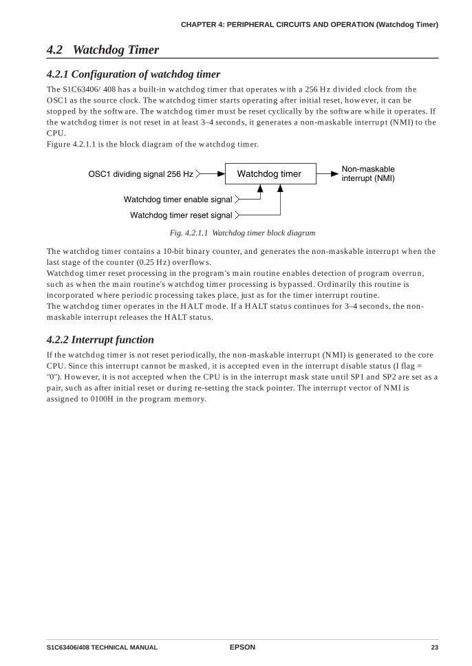
4.2.1 Configuration of watchdog timerThe S1C63406/408 has a built-in watchdog timer that operates with a 256 Hz divided clock from theOSC1 as the source clock. The watchdog timer starts operating after initial reset, however, it can bestopped by the software. The watchdog timer must be reset cyclically by the software while it operates. Ifthe watchdog timer is not reset in at least 3–4 seconds, it generates a non-maskable interrupt (NMI) to theCPU.Figure 4.2.1.1 is the block diagram of the watchdog timer.
Watchdog timer Non-maskableinterrupt (NMI)OSC1 dividing signal 256 Hz
Watchdog timer enable signal
Watchdog timer reset signal
Fig. 4.2.1.1 Watchdog timer block diagram
The watchdog timer contains a 10-bit binary counter, and generates the non-maskable interrupt when thelast stage of the counter (0.25 Hz) overflows.Watchdog timer reset processing in the program's main routine enables detection of program overrun,such as when the main routine's watchdog timer processing is bypassed. Ordinarily this routine isincorporated where periodic processing takes place, just as for the timer interrupt routine.The watchdog timer operates in the HALT mode. If a HALT status continues for 3–4 seconds, the non-maskable interrupt releases the HALT status.
4.2.2 Interrupt functionIf the watchdog timer is not reset periodically, the non-maskable interrupt (NMI) is generated to the coreCPU. Since this interrupt cannot be masked, it is accepted even in the interrupt disable status (I flag ="0"). However, it is not accepted when the CPU is in the interrupt mask state until SP1 and SP2 are set as apair, such as after initial reset or during re-setting the stack pointer. The interrupt vector of NMI isassigned to 0100H in the program memory.

24 EPSON S1C63406/408 TECHNICAL MANUAL
CHAPTER 4: PERIPHERAL CIRCUITS AND OPERATION (Watchdog Timer)
4.2.3 I/O memory of watchdog timerTable 4.2.3.1 shows the I/O address and control bits for the watchdog timer.
Table 4.2.3.1 Control bits of watchdog timer
Address CommentD3 D2
Register
D1 D0 Name Init ∗1 1 0
FF07HHLMOD 0 WDEN WDRST
R/W R R/W W
HLMOD 0 ∗3
WDENWDRST∗3
0 – ∗2
1Reset
On
EnableReset
Off
DisableInvalid
Heavy load protection
Unused
Watchdog timer enable
Watchdog timer reset (writing)
*1 Initial value at initial reset
*2 Not set in the circuit
*3 Constantly "0" when being read
WDEN: Watchdog timer enable register (FF07H•D1)Selects whether the watchdog timer is used (enabled) or not (disabled).
When "1" is written: EnabledWhen "0" is written: Disabled
Reading: Valid
When "1" is written to the WDEN register, the watchdog timer starts count operation. When "0" is written,the watchdog timer does not count and does not generate the interrupt (NMI).At initial reset, this register is set to "1".
WDRST: Watchdog timer reset (FF07H•D0)Resets the watchdog timer.
When "1" is written: Watchdog timer is resetWhen "0" is written: No operation
Reading: Always "0"
When "1" is written to WDRST, the watchdog timer is reset and restarts immediately after that. When "0"is written, no operation results.This bit is dedicated for writing, and is always "0" for reading.
4.2.4 Programming notes(1) When the watchdog timer is being used, the software must reset it within 3-second cycles.
(2) Because the watchdog timer is set in operation state by initial reset, set the watchdog timer to disabledstate (not used) before generating an interrupt (NMI) if it is not used.

S1C63406/408 TECHNICAL MANUAL EPSON 25
CHAPTER 4: PERIPHERAL CIRCUITS AND OPERATION (Oscillation Circuit)
4.3 Oscillation Circuit
4.3.1 Configuration of oscillation circuitThe S1C63406/408 has two oscillation circuits (OSC1 and OSC3). OSC1 is either a crystal or CR oscillationcircuit that supplies the operating clock to the CPU and peripheral circuits. OSC3 is a CR, crystal orceramic oscillation circuit. When processing with the S1C63406/408 requires high-speed operation, theCPU operating clock can be switched from OSC1 to OSC3 by the software. To stabilize operation of theinternal circuits, the operating voltage VD1 must be switched according to the oscillation circuit to beused. Figure 4.3.1.1 is the block diagram of this oscillation system.
Oscillation circuit control signal
CPU clock selection signal
To CPU
To peripheral circuits
Clockswitch
Oscillation systemvoltage regulator
OSC3oscillation circuit
OSC1oscillation circuit
Operating voltage selection signal
VD1VD1
VOSC
Divider
Fig. 4.3.1.1 Oscillation system block diagram
Note: The S1C63406/408 supports the SLEEP function. The OSC3 oscillation circuit stops in the SLEEPmode. The OSC1 oscillation circuit stops clock supply to the divider and peripheral circuits,however, the oscillation continues. To prevent improper operation after the CPU wakes up, be sureto run the CPU with the OSC1 clock before setting the CPU in the SLEEP mode.

26 EPSON S1C63406/408 TECHNICAL MANUAL
CHAPTER 4: PERIPHERAL CIRCUITS AND OPERATION (Oscillation Circuit)
4.3.2 OSC1 oscillation circuitThe OSC1 oscillation circuit generates the main clock for the CPU and the peripheral circuits. Eithercrystal or CR can be selected for the oscillator type by mask option. The oscillation frequency of thecrystal oscillation circuit is 32.768 kHz (Typ.) and the CR oscillation circuit is 60 kHz (Typ.).This circuit operates with the VOSC (1.3 V Typ.) voltage output from the oscillation system voltageregulator.Figure 4.3.2.1 is the block diagram of the OSC1 oscillation circuit.
VSS
CGXX
'tal1
OSC2
OSC1
RF
X
RD
X
CDX
To CPU(and peripheral circuits)
VSS
OSC2
OSC1
CCR
To CPU(and peripheral circuits)
RC
R1
(a) Crystal oscillation circuit
(b) CR oscillation circuit
Fig. 4.3.2.1 OSC1 oscillation circuit
As shown in Figure 4.3.2.1, the crystal oscillation circuit can be configured simply by connecting thecrystal oscillator (X'tal1) of 32.768 kHz (Typ.) between the OSC1 and OSC2 terminals and the trimmercapacitor (CGX) between the OSC1 and VSS terminals when crystal oscillation is selected.
The CR oscillation circuit can be configured simply by connecting the resistor RCR1 between the OSC1and OSC2 terminals when CR oscillation is selected. See Chapter 7, "Electrical Characteristics" for resis-tance value of RCR1.
Notes: • The current consumption of CR oscillation is larger than crystal oscillation.
• Be aware that the CR oscillation frequency changes slightly.Pay special attention to the circuits that use fOSC1 as the source clock, such as the timer (timelag) and the LCD frame frequency (display quality, flicker in low frequency).

S1C63406/408 TECHNICAL MANUAL EPSON 27
CHAPTER 4: PERIPHERAL CIRCUITS AND OPERATION (Oscillation Circuit)
4.3.3 OSC3 oscillation circuitThe S1C63406/408 has built-in the OSC3 oscillation circuit that generates the CPU's sub-clock (Max. 4.2MHz) for high speed operation and the source clock for peripheral circuits needing a high speed clock(programmable timer, FOUT output). The mask option enables selection of CR, crystal or ceramic oscilla-tion circuit.This circuit operates with the VD1 voltage and the voltage level must be switched when the OSC3 oscilla-tion is turned ON and OFF (see the next section for details).Figure 4.3.3.1 is the block diagram of the OSC3 oscillation circuit.
CCR
OSC3
OSC4
RC
R2
VSS
CGC
CDC Cer
amic
/X
'tal2
OSC4
OSC3
R RDC
FC
To CPU(and some peripheral circuits)
Oscillation circuit control signal
To CPU(and some peripheral circuits)
Oscillation circuit control signal
(a) CR oscillation circuit
(b) Ceramic/cryctal oscillation circuit
Fig. 4.3.3.1 OSC3 oscillation circuit
As shown in Figure 4.3.3.1, the CR oscillation circuit can be configured simply by connecting the resistorRCR2 between the OSC3 and OSC4 terminals when CR oscillation is selected. See Chapter 7, "ElectricalCharacteristics", for resistance value of RCR2.When crystal or ceramic oscillation is selected, the crystal or ceramic oscillation circuit can be configuredby connecting a crystal or ceramic oscillator (Max. 4.2 MHz) between the OSC3 and OSC4 terminals,capacitor CGC between the OSC3 and OSC4 terminals, and capacitor CDC between the OSC4 and VSS
terminals. See Chapter 7, "Electrical Characteristics", for capacitor values of CGC and CDC. To reducecurrent consumption of the OSC3 oscillation circuit, oscillation can be stopped by the software (OSCCregister).

28 EPSON S1C63406/408 TECHNICAL MANUAL
CHAPTER 4: PERIPHERAL CIRCUITS AND OPERATION (Oscillation Circuit)
4.3.4 Switching of operating voltageThe CPU system clock is switched to OSC1 or OSC3 by the software (CLKCHG register). In this case, toobtain stable operation, the operating voltage VD1 for the internal circuits must be switched by thesoftware (VDC1 and VDC0 registers). The power supply circuit supports the following four voltagelevels. When switching the VD1 level, select one according to the oscillation frequency.
1. VD1 = 1.1 V (VDC1, VDC0 = "0H")This mode is provided for low-power operation. Set this mode when the system runs with the OSC1clock (80 kHz Max.). Do not turn the OSC3 oscillation circuit on in this mode. The CLKCHG register isdisabled by the hardware in this mode.
2. VD1 = 1.3 V (VDC1, VDC0 = "1H")Set this mode when using the OSC3 CR oscillation clock (700 kHz Max.). Do not set this mode if thefrequency is higher than 700 kHz or OSC3 is not CR oscillation circuit.
3. VD1 = 1.5 V (VDC1, VDC0 = "2H")Set this mode when using the OSC3 CR oscillation clock (2.2 MHz Max.). Do not set this mode if OSC3is not CR oscillation circuit or the OSC3 CR oscillation clock more than 2.2 MHz is used. This modecan be set even if a 700 kHz or less OSC3 CR oscillation clock is used. However it is not recommendedfor low-power operation.
4. VD1 = 1.7 V (VDC1, VDC0 = "3H")Set this mode when using the OSC3 crystal, ceramic or CR oscillation clock (4.2 MHz Max.). Thismode can be set even if the OSC3 CR oscillation clock less than 2.2 MHz is used. However it is notrecommended for low-power operation.
When OSC3 is to be used as the CPU system clock, it should be done as the following procedure usingthe software: first switch the operating voltage VD1, turn the OSC3 oscillation ON after waiting 2.5 msecor more for the above operation to stabilize, switch the clock after waiting 5 msec or more for oscillationstabilization.When switching from OSC3 to OSC1, turn the OSC3 oscillation circuit OFF after switching the clock thenset the operating voltage VD1 to 1.1 V.
OSC1 → OSC3 OSC3 → OSC1
1. Set VDC (1 and 0) to "1", "2" or "3". 1. Set CLKCHG to "0" (OSC3 → OSC1).2. Maintain 2.5 msec or more. 2. Set OSCC to "0" (OSC3 oscillation OFF).3. Set OSCC to "1" (OSC3 oscillation ON). 3. Set VDC (1 and 0) to "0" (VD1 = 1.1 V).4. Maintain 5 msec or more.5. Set CLKCHG to "1" (OSC1 → OSC3).
4.3.5 Clock frequency and instruction execution timeTable 4.3.5.1 shows the instruction execution time according to each frequency of the system clock.
Table 4.3.5.1 Clock frequency and instruction execution time
Clock frequency
OSC1: 32.768 kHz
OSC1: 60 kHz
OSC3: 2 MHz
OSC3: 3.58 MHz
OSC3: 4 MHz
Instruction execution time (µsec)
1-cycle instruction 2-cycle instruction 3-cycle instruction
61 122 183
33 67 100
1 2 3
0.56 1.12 1.68
0.5 1 1.5

S1C63406/408 TECHNICAL MANUAL EPSON 29
CHAPTER 4: PERIPHERAL CIRCUITS AND OPERATION (Oscillation Circuit)
4.3.6 I/O memory of oscillation circuitTable 4.3.6.1 shows the I/O address and the control bits for the oscillation circuit.
Table 4.3.6.1 Control bits of oscillation circuit
Address CommentD3 D2
Register
D1 D0 Name Init ∗ 1 1 0
FF00HCLKCHG OSCC VDC1 VDC0
R/W
CLKCHGOSCCVDC1VDC0
0000
OSC3On
OSC1Off
CPU clock switch
OSC3 oscillation On/Off
CPU operating
voltage switch0
1.11
1.32
1.53
1.7[VDC1, 0]VD1 (V)
*1 Initial value at initial reset
*2 Not set in the circuit
*3 Constantly "0" when being read
VDC1, VDC0: CPU operating voltage switching register (FF00H•D1, D0)Switchs the operating voltage VD1.
Table 4.3.6.2 CPU operating voltage and oscillation frequencyVDC1
1100
VDC01010
VD1
1.7 V1.5 V1.3 V1.1 V
Oscillation circuit (frequency)OSC3 CR, ceramic or crystal (4.2 MHz max.)OSC3 CR (2.2 MHz max.)OSC3 CR (700 kHz max.)OSC1 Crystal or CR (80 kHz max.)
When switching the CPU system clock, the operating voltage VD1 should also be switched according tothe clock frequency.When switching from OSC1 to OSC3, first set VD1 to the appropriate level. After that maintain 2.5 msec ormore, and then turn the OSC3 oscillation ON.When switching from OSC3 to OSC1, turn the OSC3 oscillation OFF after switching to OSC1, and then setVD1 to 1.1 V to reduce current consumption. When the VDC register is set to "0", do not turn the OSC3oscillation ON.At initial reset, this register is set to "0".
OSCC: OSC3 oscillation control register (FF00H•D2)Controls oscillation ON/OFF for the OSC3 oscillation circuit.
When "1" is written: OSC3 oscillation ONWhen "0" is written: OSC3 oscillation OFF
Reading: Valid
When it is necessary to operate the CPU at high speed, set OSCC to "1". At other times, set it to "0" toreduce current consumption. Furthermore, it is necessary to switch the operating voltage VD1 whenturning the OSC3 oscillation circuit ON and OFF.At initial reset, this register is set to "0".
CLKCHG: CPU system clock switching register (FF00H•D3)The CPU's operation clock is selected with this register.
When "1" is written: OSC3 clock is selectedWhen "0" is written: OSC1 clock is selected
Reading: Valid
When the CPU clock is to be OSC3, set CLKCHG to "1"; for OSC1, set CLKCHG to "0".After turning the OSC3 oscillation ON (OSCC = "1"), switching of the clock should be done after waiting5 msec or more.When OSC3 oscillation is OFF (OSCC = "0"), setting of CLKCHG = "1" becomes invalid and switching toOSC3 is not performed.At initial reset, this register is set to "0".
30 EPSON S1C63406/408 TECHNICAL MANUAL
CHAPTER 4: PERIPHERAL CIRCUITS AND OPERATION (Oscillation Circuit)
4.3.7 Programming notes(1) When switching the CPU system clock from OSC1 to OSC3, first set VD1. After that maintain 2.5 msec
or more, and then turn the OSC3 oscillation ON.When switching from OSC3 to OSC1, set VD1 after switching to OSC1 and turning the OSC3 oscilla-tion OFF.
(2) It takes at least 5 msec from the time the OSC3 oscillation circuit goes ON until the oscillation stabi-lizes. Consequently, when switching the CPU operation clock from OSC1 to OSC3, do this after aminimum of 5 msec have elapsed since the OSC3 oscillation went ON.Further, the oscillation stabilization time varies depending on the external oscillator characteristicsand conditions of use, so allow ample margin when setting the wait time.
(3) When switching the clock form OSC3 to OSC1, use a separate instruction for switching the OSC3oscillation OFF. An error in the CPU operation can result if this processing is performed at the sametime by the one instruction.
(4) The S1C63406/408 supports the SLEEP function. The OSC3 oscillation circuit stops in the SLEEPmode. The OSC1 oscillation circuit stops clock supply to the divider and peripheral circuits, however,the oscillation continues. To prevent improper operation after the CPU wakes up, be sure to run theCPU with the OSC1 clock before setting the CPU in the SLEEP mode.

S1C63406/408 TECHNICAL MANUAL EPSON 31
CHAPTER 4: PERIPHERAL CIRCUITS AND OPERATION (Input Ports)
4.4 Input Ports (K00–K03)
K0x
Mask option
Address
VDD
Interruptrequest
Dat
a bu
s
VSS
Fig. 4.4.1.1 Configuration of input port
4.4.1 Configuration of input portsThe S1C63406/408 has four bits of general-purposeinput ports. Each of the input port terminals (K00–K03)provides internal pull-up resistor. Pull-up resistor canbe selected for each bit with the mask option.Figure 4.4.1.1 shows the configuration of input port.Selection of "With pull-up resistor" with the maskoption suits input from the push switch, key matrix,and so forth. When "Gate direct" is selected, the portcan be used for slide switch input and interfacing withother LSIs.
4.4.2 Mask optionInternal pull-up resistor can be selected for each of the four bits of the input ports (K00–K03) with theinput port mask option.When "Gate direct" is selected, take care that the floating status does not occur for the input. Select "Withpull-up resistor" for input ports that are not being used.
4.4.3 Interrupt functionAll four bits of the input ports (K00–K03) provide the interrupt function. The conditions for issuing aninterrupt can be set by the software. Further, whether to mask the interrupt function can be selected bythe software.Figure 4.4.3.1 shows the configuration of K00–K03 interrupt circuit.
Dat
a bu
s
Address
Address
Address
Address
Input comparison register (KCP00)
Noiserejector
MUX
Interrupt selection register (SIK00)
Interrupt factorflag (IK00)
Address
Interrupt mask register (EIK00)
Address
Noise reject selection register (K0NR1, 0)
K00
K01K02
K03
Sleepcancelation
Interruptrequest
Fig. 4.4.3.1 Input interrupt circuit configuration

32 EPSON S1C63406/408 TECHNICAL MANUAL
CHAPTER 4: PERIPHERAL CIRCUITS AND OPERATION (Input Ports)
The interrupt selection registers (SIK00–SIK03) and input comparison registers (KCP00–KCP03) areindividually provided for the input ports K00–K03.
The interrupt selection registers (SIK0x) select the ports to be used for generating input interrupts orcanceling the SLEEP mode. Writing "1" into an interrupt selection register incorporates that port into theinterrupt generation conditions. The changing the port where the interrupt selection register has been setto "0" does not affect the generation of the interrupt.
The input interrupt timing can select that the interrupt be generated at the rising edge of the input or thatit be generated at the falling edge according to the set value of the input comparison registers (KCP0x).
By setting these two conditions, an interrupt request signal and a wake up signal are generated at therising or falling edge (selected by KCP0x) of the signal input to the port (selected by SIK0x).
When an interrupt factor is generated, the interrupt factor flag (IK00–IK03) is set to "1". At the same time,an interrupt rquest is generated to the CPU if the corresponding interrupt mask register (EIK00–EIK03) isset to "1".When the interrupt mask registers (EIK0x) is set to "0", the interrupt request is masked and no interrupt isgenerated to the CPU. However, the SLEEP mode can be cancelled regardless of the interrupt enableregister setting.
The input interrupt circuit has a noise rejector to avoid unnecessary interrupt generation due to noise orchattering. This noise rejector allows selection of a noise-reject width from among three types shown inTable 4.4.3.1. Use the K0NR1 and K0NR0 registers to select a noise-reject width. If a pulse shorter than theselected width is input to the port, an interrupt is not generated. When high speed response is required,the noise rejecter can be disconnected from the input line.
Table 4.4.3.1 Setting up noise rejector
K0NR1
1
1
0
0
K0NR0
1
0
1
0
Noise-reject width
7.8 msec
2.0 msec
0.5 msec
OFF (bypassed)
(When fOSC1 = 32.768 kHz)
Notes: • Be sure to turn the noise rejector OFF before executing the SLP instruction.
• Reactivating from SLEEP status can only be done by generation of an input interrupt factor.Therefore when using the SLEEP function, it is necessary to set the interrupt selection register(SIK0x = "1") of the port to be used for releasing SLEEP status before executing the SLPinstruction. Furthermore, enable the input port interrupt using the corresponding interrupt maskregister (EIK0x = "1") before executing the SLP instruction to run input interrupt handler routineafter SLEEP status is released.
• Each input port (K00–K03) has a different interrupt factor, thus the input interrupt is controlledindividually. Be aware that this interrupt configuration is different from that of the previousmodels.

S1C63406/408 TECHNICAL MANUAL EPSON 33
CHAPTER 4: PERIPHERAL CIRCUITS AND OPERATION (Input Ports)
4.4.4 I/O memory of input portsTable 4.4.4.1 shows the I/O addresses and the control bits for the input ports.
Table 4.4.4.1 Control bits of input ports
Address CommentD3 D2
Register
D1 D0 Name Init ∗1 1 0
FF42HK03 K02 K01 K00
R
K03K02K01K00
– ∗2
– ∗2
– ∗2
– ∗2
HighHighHighHigh
LowLowLowLow
K00–K03 input port data
FF43H0 0 K0NR1 K0NR0
R R/W
0 ∗3
0 ∗3
K0NR1K0NR0
– ∗2
– ∗2
00
Unused
Unused
K0 interrupt
noise rejector0
Off1
0.5ms2
2.0ms3
7.8ms[K0NR1, 0]NR
FF54HSIK03 SIK02 SIK01 SIK00
R/W
SIK03SIK02SIK01SIK00
0000
EnableEnableEnableEnable
DisableDisableDisableDisable
K00–K03 interrupt selection register
FF55HKCP03 KCP02 KCP01 KCP00
R/W
KCP03KCP02KCP01KCP00
1111
K00–K03 input comparison register
FFEBHEIK03 EIK02 EIK01 EIK00
R/W
EIK03EIK02EIK01EIK00
0000
EnableEnableEnableEnable
MaskMaskMaskMask
Interrupt mask register (K03)
Interrupt mask register (K02)
Interrupt mask register (K01)
Interrupt mask register (K00)
FFFBHIK03 IK02 IK01 IK00
R/W
IK03IK02IK01IK00
0000
(R)Yes(W)
Reset
(R)No(W)
Invalid
Interrupt factor flag (K03)
Interrupt factor flag (K02)
Interrupt factor flag (K01)
Interrupt factor flag (K00)
*1 Initial value at initial reset
*2 Not set in the circuit
*3 Constantly "0" when being read
K00–K03: K0 port input port data (FF42H)Input data of the input port terminals can be read with these registers.
When "1" is read: High levelWhen "0" is read: Low level
Writing: Invalid
The reading is "1" when the terminal voltage of the four bits of the input ports (K00–K03) goes high(VDD), and "0" when the voltage goes low (VSS).These bits are dedicated for reading, so writing cannot be done.
SIK00–SIK03: K0 port interrupt selection register (FF54H)Selects the ports to be used for the K00–K03 input interrupts.
When "1" is written: EnableWhen "0" is written: Disable
Reading: Valid
Enables the interrupt for the input ports (K00–K03) for which "1" has been written into the interruptselection registers (SIK00–SIK03). The input port set for "0" does not affect the interrupt generationcondition.Reactivating from SLEEP status can only be done by generation of an input interrupt factor. Thereforewhen using the SLEEP function, it is necessary to set the interrupt selection register (SIK0x = "1") of theport to be used for releasing SLEEP status before executing the SLP instruction.At initial reset, these registers are set to "0".
34 EPSON S1C63406/408 TECHNICAL MANUAL
CHAPTER 4: PERIPHERAL CIRCUITS AND OPERATION (Input Ports)
KCP00–KCP03: K0 port input comparison register (FF55H)Interrupt conditions for terminals K00–K03 can be set with these registers.
When "1" is written: Falling edgeWhen "0" is written: Rising edge
Reading: Valid
The interrupt conditions can be set for the rising or falling edge of input for each of the four bits (K00–K03), through the input comparison registers (KCP00–KCP03).A comparison is done only with the ports that are enabled by the interrupt among K00–K03 by means ofthe SIK00–SIK03 registers.At initial reset, these registers are set to "1".
K0NR0, K0NR1: K0 interrupt noise rejector selection register (FF43H•D0, D1)Selects the noise-reject width.
Table 4.4.4.2 Setting up noise rejector
K0NR1
1
1
0
0
K0NR0
1
0
1
0
Noise-reject width
7.8 msec
2.0 msec
0.5 msec
OFF (bypassed)
(When fOSC1 = 32.768 kHz)
Be sure to turn the noise rejector OFF before executing the SLP instruction.At initial reset, these registers are set to "0".
EIK00–EIK03: K0 input interrupt mask register (FFEBH)Masks the input interrupt request to the CPU.
When "1" is written: EnableWhen "0" is written: Mask
Reading: Valid
When "1" is written to the EIK0x register, the input interrupt request will be generated to the CPU. When"0" is written, no input interrupt will be generated from the corresponding port.The wake up signal to release the SLEEP mode will be generated even if this register is set to "0". How-ever, enable the input port interrupt using the corresponding interrupt mask register before executing theSLP instruction to run input interrupt handler routine after SLEEP status is released.At initial reset, this register is set to "0".
IK00–IK03: K0 input interrupt factor flag (FFFBH)This flag indicates the occurrence of input interrupt.
When "1" is read: Interrupt has occurredWhen "0" is read: Interrupt has not occurred
When "1" is written: Flag is resetWhen "0" is written: Invalid
IK0x is the interrupt factor flag corresponding to the K0x port. From the status of this flag, the softwarecan decide whether an input interrupt has occurred.The interrupt factor flag is set to "1" when the interrupt condition is established regardless of the interruptmask register setting. However, the interrupt does not occur to the CPU when the interrupt is masked.This flag is reset to "0" by writing "1".After an interrupt occurs, the same interrupt will occur again if the interrupt enabled state (I flag = "1") isset or the RETI instruction is executed unless the interrupt factor flag is reset. Therefore, be sure to reset(write "1" to) the interrupt factor flag in the interrupt service routine before shifting to the interruptenabled state.At initial reset, this flag is set to "0".
S1C63406/408 TECHNICAL MANUAL EPSON 35
CHAPTER 4: PERIPHERAL CIRCUITS AND OPERATION (Input Ports)
4.4.5 Programming notes(1) When input ports are changed from low to high by pull-up resistors, the rise of the waveform is
delayed on account of the time constant of the pull-up resistor and input gate capacitance. Hence,when fetching input ports, set an appropriate waiting time.Particular care needs to be taken of the key scan during key matrix configuration.Make this waiting time the amount of time or more calculated by the following expression.10 × C × R
C: terminal capacitance 5 pF + parasitic capacitance ? pFR: pull-up resistance 300 kΩ
(2) Be sure to turn the noise rejector OFF before executing the SLP instruction.
(3) Reactivating from SLEEP status can only be done by generation of an input interrupt factor. Thereforewhen using the SLEEP function, it is necessary to set the interrupt selection register (SIK0x = "1") ofthe port to be used for releasing SLEEP status before executing the SLP instruction. Furthermore,enable the input port interrupt using the corresponding interrupt mask register (EIK0x = "1") beforeexecuting the SLP instruction to run input interrupt handler routine after SLEEP status is released.
(4) Each input port (K00–K03) has a different interrupt factor, thus the input interrupt is controlledindividually. Be aware that this interrupt configuration is different from that of the previous models.
(5) The K03 terminal functions as the clock input terminal for the programmable timer, and the inputsignal is shared with the input port and the programmable timer. Therefore, when the K03 terminal isset to the clock input terminal for the programmable timer, take care of the interrupt setting.
(6) After an interrupt occurs, the same interrupt will occur again if the interrupt enabled state (I flag ="1") is set or the RETI instruction is executed unless the interrupt factor flag is reset. Therefore, be sureto reset (write "1" to) the interrupt factor flag in the interrupt service routine before shifting to theinterrupt enabled state.
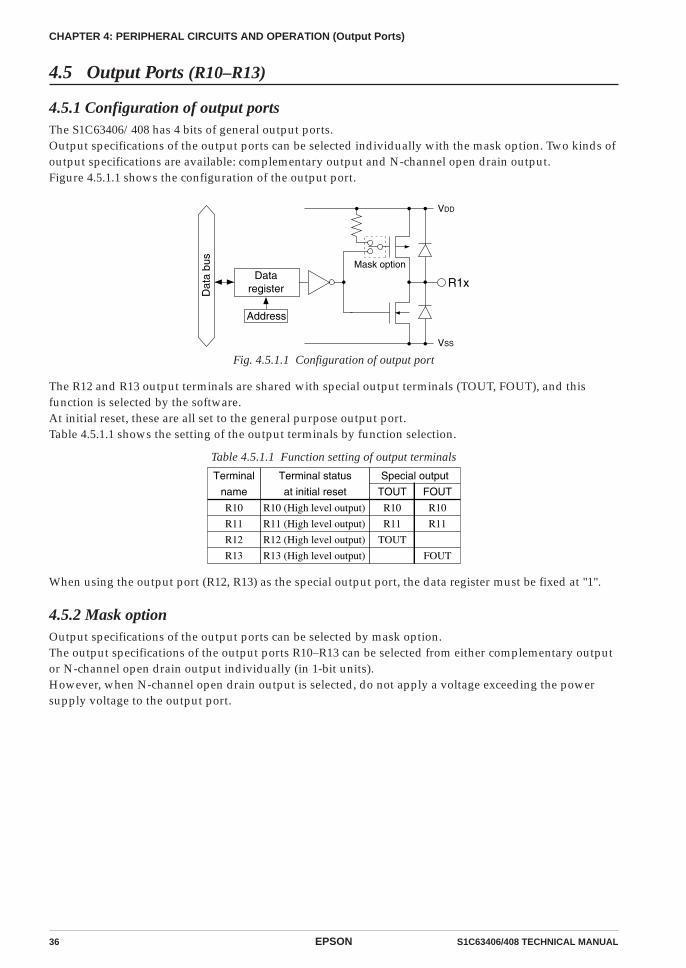
36 EPSON S1C63406/408 TECHNICAL MANUAL
CHAPTER 4: PERIPHERAL CIRCUITS AND OPERATION (Output Ports)
4.5 Output Ports (R10–R13)
4.5.1 Configuration of output portsThe S1C63406/408 has 4 bits of general output ports.Output specifications of the output ports can be selected individually with the mask option. Two kinds ofoutput specifications are available: complementary output and N-channel open drain output.Figure 4.5.1.1 shows the configuration of the output port.
VDD
VSS
R1x
Dat
a bu
s
Address
Dataregister
Mask option
Fig. 4.5.1.1 Configuration of output port
The R12 and R13 output terminals are shared with special output terminals (TOUT, FOUT), and thisfunction is selected by the software.At initial reset, these are all set to the general purpose output port.Table 4.5.1.1 shows the setting of the output terminals by function selection.
Table 4.5.1.1 Function setting of output terminals
Terminal
name
R10
R11
R12
R13
Terminal status
at initial reset
R10 (High level output)
R11 (High level output)
R12 (High level output)
R13 (High level output)
Special output
TOUT FOUT
R10 R10
R11 R11
TOUT
FOUT
When using the output port (R12, R13) as the special output port, the data register must be fixed at "1".
4.5.2 Mask optionOutput specifications of the output ports can be selected by mask option.The output specifications of the output ports R10–R13 can be selected from either complementary outputor N-channel open drain output individually (in 1-bit units).However, when N-channel open drain output is selected, do not apply a voltage exceeding the powersupply voltage to the output port.
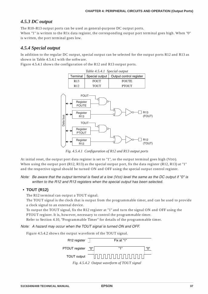
S1C63406/408 TECHNICAL MANUAL EPSON 37
CHAPTER 4: PERIPHERAL CIRCUITS AND OPERATION (Output Ports)
4.5.3 DC outputThe R10–R13 output ports can be used as general-purpose DC output ports.When "1" is written to the R1x data register, the corresponding output port terminal goes high. When "0"is written, the port terminal goes low.
4.5.4 Special outputIn addition to the regular DC output, special output can be selected for the output ports R12 and R13 asshown in Table 4.5.4.1 with the software.Figure 4.5.4.1 shows the configuration of the R12 and R13 output ports.
Table 4.5.4.1 Special outputTerminal
R13
R12
Special output
FOUT
TOUT
Output control register
FOUTE
PTOUT
Dat
a bu
s
RegisterPTOUT
RegisterR12
TOUT
R12(TOUT)
RegisterFOUTE
RegisterR13
FOUT
R13(FOUT)
Fig. 4.5.4.1 Configuration of R12 and R13 output ports
At initial reset, the output port data register is set to "1", so the output terminal goes high (VDD).When using the output port (R12, R13) as the special output port, fix the data register (R12, R13) at "1"and the respective signal should be turned ON and OFF using the special output control register.
Note: Be aware that the output terminal is fixed at a low (VSS) level the same as the DC output if "0" iswritten to the R12 and R13 registers when the special output has been selected.
• TOUT (R12)The R12 terminal can output a TOUT signal.The TOUT signal is the clock that is output from the programmable timer, and can be used to providea clock signal to an external device.To output the TOUT signal, fix the R12 register at "1" and turn the signal ON and OFF using thePTOUT register. It is, however, necessary to control the programmable timer.Refer to Section 4.10, "Programmable Timer" for details of the programmable timer.
Note: A hazard may occur when the TOUT signal is turned ON and OFF.
Figure 4.5.4.2 shows the output waveform of the TOUT signal.
R12 register
PTOUT register
TOUT output
Fix at "1"
"1""0" "0"
Fig. 4.5.4.2 Output waveform of TOUT signal

38 EPSON S1C63406/408 TECHNICAL MANUAL
CHAPTER 4: PERIPHERAL CIRCUITS AND OPERATION (Output Ports)
• FOUT (R13)The R13 terminal can output a FOUT signal.The FOUT signal is a clock that is output from the oscillation circuit or a clock that the fOSC1 clock hasdivided in the internal circuit, and can be used to provide a clock signal to an external device.To output the FOUT signal, fix the R13 register at "1" and turn the signal ON and OFF using theFOUTE register.The frequency of the output clock may be selected from among 8 types shown in Table 4.5.4.2 bysetting the FOFQ0–FOFQ2 registers.
Table 4.5.4.2 FOUT clock frequency
FOFQ1
1
1
0
0
1
1
0
0
FOFQ2
1
1
1
1
0
0
0
0
FOFQ0
1
0
1
0
1
0
1
0
Clock frequency
fOSC3
fOSC3/2
fOSC1
fOSC1/4
fOSC1/8
fOSC1/16
fOSC1/32
fOSC1/64fOSC1: Clock that is output from the OSC1 oscillation circuitfOSC3: Clock that is output from the OSC3 oscillation circuit
When fOSC3 is selected for the FOUT signal frequency, it is necessary to control the OSC3 oscillationcircuit before output.Refer to Section 4.3, "Oscillation Circuit", for the control and notes.
Note: A hazard may occur when the FOUT signal is turned ON and OFF.
Figure 4.5.4.3 shows the output waveform of the FOUT signal.
R13 register
FOUTE register
FOUT output
Fix at "1"
"1""0" "0"
Fig. 4.5.4.3 Output waveform of FOUT signal
S1C63406/408 TECHNICAL MANUAL EPSON 39
CHAPTER 4: PERIPHERAL CIRCUITS AND OPERATION (Output Ports)
4.5.5 I/O memory of output portsTable 4.5.5.1 shows the I/O addresses and control bits for the output ports.
Table 4.5.5.1 Control bits of output ports
Address CommentD3 D2
Register
D1 D0 Name Init ∗1 1 0
FF06HFOUTE FOFQ2 FOFQ1 FOFQ0
R/W
FOUTEFOFQ2FOFQ1FOFQ0
0000
Enable Disable FOUT enable
FOUT
frequency
selection
0fOSC1/64
4fOSC1/4
1fOSC1/32
5fOSC1
2fOSC1/16
6fOSC3/2
3fOSC1/8
7fOSC3
[FOFQ2–0]Frequency[FOFQ2–0]Frequency
FF46H
R13 R12 R11 R10
R/W
R13
R12
R11R10
1
1
11
High
High
HighHigh
Low
Low
LowLow
R13 output port data (FOUTE=0)
Fix at "1" when FOUT is used (FOUTE=1)
R12 output port data (PTOUT=0)
Fix at "1" when TOUT is used (PTOUT=1)
R11 output port data
R10 output port data
CHSELPTOUTCKSEL1CKSEL0
0000
Timer1On
OSC3OSC3
Timer0Off
OSC1OSC1
TOUT output channel selection
TOUT output control
Prescaler 1 source clock selection
Prescaler 0 source clock selectionR/W
FFC1HCHSEL PTOUT CKSEL1 CKSEL0
*1 Initial value at initial reset
*2 Not set in the circuit
*3 Constantly "0" when being read
R10–R13: R1 output port data register (FF46H)Set the output data for the output ports.
When "1" is written: High level outputWhen "0" is written: Low level output
Reading: Valid
The output port terminals output the data written in the corresponding data registers without changingit. When "1" is written to the register, the output port terminal goes high (VDD), and when "0" is written,the output port terminal goes low (VSS).When the output ports R12 and R13 are used for special output (TOUT, FOUT), fix the R12 register andthe R13 register at "1".At initial reset, these registers are all set to "1".
PTOUT: TOUT output control register (FFC1H•D2)Controls the TOUT output.
When "1" is written: TOUT output ONWhen "0" is written: TOUT output OFF
Reading: Valid
By writing "1" to the PTOUT register when the R12 register has been set to "1", the TOUT signal is outputfrom the R12 terminal. When "0" is written, the R12 terminal goes high (VDD).When using the R12 output port for DC output, fix this register at "0".At initial reset, this register is set to "0".
FOUTE: FOUT output control register (FF06H•D3)Controls the FOUT output.
When "1" is written: FOUT output ONWhen "0" is written: FOUT output OFF
Reading: Valid
By writing "1" to the FOUTE register when the R13 register has been set to "1" , an FOUT signal is outputfrom the R13 terminal. When "0" is written, the R13 terminal goes high (VDD).When using the R13 output port for DC output, fix this register at "0".At initial reset, this register is set to "0".
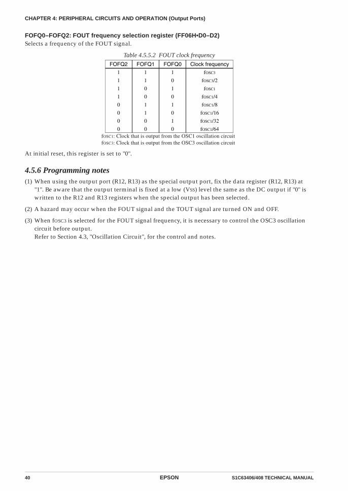
40 EPSON S1C63406/408 TECHNICAL MANUAL
CHAPTER 4: PERIPHERAL CIRCUITS AND OPERATION (Output Ports)
FOFQ0–FOFQ2: FOUT frequency selection register (FF06H•D0–D2)Selects a frequency of the FOUT signal.
Table 4.5.5.2 FOUT clock frequency
FOFQ1
1
1
0
0
1
1
0
0
FOFQ2
1
1
1
1
0
0
0
0
FOFQ0
1
0
1
0
1
0
1
0
Clock frequency
fOSC3
fOSC3/2
fOSC1
fOSC1/4
fOSC1/8
fOSC1/16
fOSC1/32
fOSC1/64fOSC1: Clock that is output from the OSC1 oscillation circuitfOSC3: Clock that is output from the OSC3 oscillation circuit
At initial reset, this register is set to "0".
4.5.6 Programming notes(1) When using the output port (R12, R13) as the special output port, fix the data register (R12, R13) at
"1". Be aware that the output terminal is fixed at a low (VSS) level the same as the DC output if "0" iswritten to the R12 and R13 registers when the special output has been selected.
(2) A hazard may occur when the FOUT signal and the TOUT signal are turned ON and OFF.
(3) When fOSC3 is selected for the FOUT signal frequency, it is necessary to control the OSC3 oscillationcircuit before output.Refer to Section 4.3, "Oscillation Circuit", for the control and notes.

S1C63406/408 TECHNICAL MANUAL EPSON 41
CHAPTER 4: PERIPHERAL CIRCUITS AND OPERATION (I/O Ports)
4.6 I/O Ports (P20–P23)
4.6.1 Configuration of I/O portsThe S1C63406/408 has four bits of general-purpose I/O ports.Figure 4.6.1.1 shows the configuration of the I/O port.
Address
DataregisterD
ata
bus
P2XAddress
Address
Address
I/O controlregister (IOC)
Pull-up controlregister (PPL)
VDD
Fig. 4.6.1.1 Configuration of I/O port
The I/O port terminals P20–P23 are shared with the serial interface input/output terminals. The softwarecan select the function to be used.At initial reset, these terminals are all set to the I/O port.Table 4.6.1.1 shows the setting of the input/output terminals by function selection.
Table 4.6.1.1 Function setting of input/output terminals
Terminal
P20
P21
P22
P23
Terminal status
at initial reset
P20 (Input & pull-up)
P21 (Input & pull-up)
P22 (Input & pull-up)
P23 (Input & pull-up)
Serial I/F
Master Slave Async.
SIN(I) SIN(I) SIN(I)
SOUT(O) SOUT(O) SOUT(O)
SCLK(O) SCLK(I) P22
P23 SRDY(O) P23
When these ports are used as I/O ports, the ports can be set to either input mode or output mode indi-vidually (in 1-bit unit). Modes can be set by writing data to the I/O control registers.Refer to Section 4.11, "Serial Interface", for control of the serial interface.

42 EPSON S1C63406/408 TECHNICAL MANUAL
CHAPTER 4: PERIPHERAL CIRCUITS AND OPERATION (I/O Ports)
4.6.2 Mask optionIn the I/O ports, the output specification during output mode can be selected from either complementaryoutput or N-channel open drain output in 1-bit units.When N-channel open drain output is selected, do not apply a voltage exceeding the power supplyvoltage to the port.
The output specification selected by mask option are effective even when I/O ports are used as the serialinterface output port.
4.6.3 I/O control registers and input/output modeInput or output mode can be set for the I/O ports by writing data into the corresponding I/O controlregisters IOC2x.
To set the input mode, write "0" to the I/O control register. When an I/O port is set to input mode, itbecomes high impedance status and works as an input port.However, when the pull-up explained in the following section has been set by software, the input line ispulled up only during this input mode.
To set the output mode, write "1" is to the I/O control register. When an I/O port is set to output mode , itworks as an output port, it outputs a high level (VDD) when the port output data is "1", and a low level(VSS) when the port output data is "0".
If perform the read out in each mode; when output mode, the register value is read out, and when inputmode, the port value is read out.
At initial reset, the I/O control registers are set to "0", and the I/O ports enter the input mode.
The I/O control registers of the ports that are set as input/output for the serial interface can be used asgeneral purpose registers that do not affect the I/O control. (See Table 4.6.1.1.)
4.6.4 Pull-up during input modeA pul-up resistor that operates during the input mode is built into each I/O port of the S1C63406/408.
The pull-up resistor becomes effective by writing "1" to the pull-up control register PPL2x that corre-sponds to each port, and the input line is pulled up during the input mode. When "0" has been written,no pull-up is done.At initial reset, the pull-up control registers are set to "1".
The pull-up control registers of the ports, that are set as output for the serial interface, can be used asgeneral purpose registers that do not affect the pull-up control. (See Table 4.6.1.1.)The pull-up control registers of the port, that are set as input for the serial interface, function the same asthe I/O port.
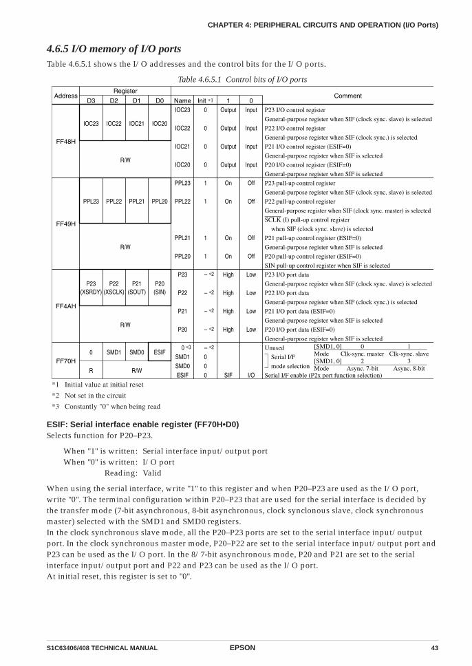
S1C63406/408 TECHNICAL MANUAL EPSON 43
CHAPTER 4: PERIPHERAL CIRCUITS AND OPERATION (I/O Ports)
4.6.5 I/O memory of I/O portsTable 4.6.5.1 shows the I/O addresses and the control bits for the I/O ports.
Table 4.6.5.1 Control bits of I/O ports
Address CommentD3 D2
Register
D1 D0 Name Init ∗1 1 0
FF49H
PPL23 PPL22 PPL21 PPL20
R/W
PPL23
PPL22
PPL21
PPL20
1
1
1
1
On
On
On
On
Off
Off
Off
Off
P23 pull-up control register
General-purpose register when SIF (clock sync. slave) is selected
P22 pull-up control register
General-purpose register when SIF (clock sync. master) is selected
SCLK (I) pull-up control register
when SIF (clock sync. slave) is selected
P21 pull-up control register (ESIF=0)
General-purpose register when SIF is selected
P20 pull-up control register (ESIF=0)
SIN pull-up control register when SIF is selected
FF48H
IOC23 IOC22 IOC21 IOC20
R/W
IOC23
IOC22
IOC21
IOC20
0
0
0
0
Output
Output
Output
Output
Input
Input
Input
Input
P23 I/O control register
General-purpose register when SIF (clock sync. slave) is selected
P22 I/O control register
General-purpose register when SIF (clock sync.) is selected
P21 I/O control register (ESIF=0)
General-purpose register when SIF is selected
P20 I/O control register (ESIF=0)
General-purpose register when SIF is selected
FF4AH
P23(XSRDY)
P22(XSCLK)
P21(SOUT)
P20(SIN)
R/W
P23
P22
P21
P20
– ∗2
– ∗2
– ∗2
– ∗2
High
High
High
High
Low
Low
Low
Low
P23 I/O port data
General-purpose register when SIF (clock sync. slave) is selected
P22 I/O port data
General-purpose register when SIF (clock sync.) is selected
P21 I/O port data (ESIF=0)
General-purpose register when SIF is selected
P20 I/O port data (ESIF=0)
General-purpose register when SIF is selected0
Clk-sync. master2
Async. 7-bit
1Clk-sync. slave
3Async. 8-bit
[SMD1, 0]Mode[SMD1, 0]Mode
FF70H0 SMD1 SMD0 ESIF
R R/W
0 ∗3
SMD1SMD0ESIF
– ∗2
000 SIF I/O
Unused
Serial I/F
mode selection
Serial I/F enable (P2x port function selection)
*1 Initial value at initial reset
*2 Not set in the circuit
*3 Constantly "0" when being read
ESIF: Serial interface enable register (FF70H•D0)Selects function for P20–P23.
When "1" is written: Serial interface input/output portWhen "0" is written: I/O port
Reading: Valid
When using the serial interface, write "1" to this register and when P20–P23 are used as the I/O port,write "0". The terminal configuration within P20–P23 that are used for the serial interface is decided bythe transfer mode (7-bit asynchronous, 8-bit asynchronous, clock synclonous slave, clock synchronousmaster) selected with the SMD1 and SMD0 registers.In the clock synchronous slave mode, all the P20–P23 ports are set to the serial interface input/outputport. In the clock synchronous master mode, P20–P22 are set to the serial interface input/output port andP23 can be used as the I/O port. In the 8/7-bit asynchronous mode, P20 and P21 are set to the serialinterface input/output port and P22 and P23 can be used as the I/O port.At initial reset, this register is set to "0".
44 EPSON S1C63406/408 TECHNICAL MANUAL
CHAPTER 4: PERIPHERAL CIRCUITS AND OPERATION (I/O Ports)
P20–P23: P2 I/O port data register (FF4AH)I/O port data can be read and output data can be set through these registers.
• When writing data
When "1" is written: High levelWhen "0" is written: Low level
When an I/O port is set to the output mode, the written data is output unchanged from the I/O portterminal. When "1" is written as the port data, the port terminal goes high (VDD), and when "0" is written,the terminal goes low (VSS).Port data can be written also in the input mode.
• When reading data
When "1" is read: High levelWhen "0" is read: Low level
The terminal voltage level of the I/O port is read out. When the I/O port is in the input mode the voltagelevel being input to the port terminal can be read out; in the output mode the register value can be read.When the terminal voltage is high (VDD) the port data that can be read is "1", and when the terminalvoltage is low (VSS) the data is "0".When the PPL register is set to "1", the built-in pull-up resister goes ON during input mode, so that theI/O port terminal is pulled up.
The data registers of the port, which are set for the input/output of the serial interface, become general-purpose registers that do not affect the input/output.
Note: When in the input mode, I/O ports are changed from low to high by pull-up resistor, the rise of thewaveform is delayed on account of the time constant of the pull-up resistor and input gate capaci-tance. Hence, when fetching input ports, set an appropriate wait time.Particular care needs to be taken of the key scan during key matrix configuration.Make this waiting time the amount of time or more calculated by the following expression.10 × C × R
C: terminal capacitance 5 pF + parasitic capacitance ? pFR: pull-up resistance 300 kΩ
IOC20–IOC23: P2 port I/O control register (FF48H)The input and output modes of the I/O ports are set with these registers.
When "1" is written: Output modeWhen "0" is written: Input mode
Reading: Valid
The input and output modes of the I/O ports are set in 1-bit unit.Writing "1" to the I/O control register makes the corresponding I/O port enter the output mode, andwriting "0" induces the input mode.At initial reset, these registers are all set to "0", so the I/O ports are in the input mode.The I/O control registers of the port, which are set for the input/output of the serial interface, becomegeneral-purpose registers that do not affect the input/output.
S1C63406/408 TECHNICAL MANUAL EPSON 45
CHAPTER 4: PERIPHERAL CIRCUITS AND OPERATION (I/O Ports)
PPL20–PPL23: P2 port pull-up control register (FF49H)The pull-up during the input mode are set with these registers.
When "1" is written: pull-up ONWhen "0" is written: pull-up OFF
Reading: Valid
The built-in pull-up resistor which is turned ON during input mode is set to enable in 1-bit units.By writing "1" to the pull-up control register, the corresponding I/O ports are pulled up (during inputmode), while writing "0" turns the pull-up function OFF.At initial reset, these registers are all set to "1", so the pull-up function is set to ON.
The pull-up control registers of the ports that are set as output for the serial interface can be used asgeneral purpose registers that do not affect the pull-up control.The pull-up control registers of the port that are set as input for the serial interface function the same asthe I/O port.
4.6.6 Programming noteWhen in the input mode, I/O ports are changed from low to high by pull-up resistor, the rise of thewaveform is delayed on account of the time constant of the pull-up resistor and input gate capacitance.Hence, when fetching input ports, set an appropriate wait time.Particular care needs to be taken of the key scan during key matrix configuration.Make this waiting time the amount of time or more calculated by the following expression.10 × C × R
C: terminal capacitance 5 pF + parasitic capacitance ? pFR: pull-up resistance 300 kΩ

46 EPSON S1C63406/408 TECHNICAL MANUAL
CHAPTER 4: PERIPHERAL CIRCUITS AND OPERATION (LCD Driver)
4.7 LCD Driver
4.7.1 Configuration of LCD driverThe S1C63406 has 9 common terminals (COM0–COM8) and 60 segment terminals (SEG0–SEG59), so thatit can drive a dot matrix type LCD with a maximum of 540 (60 × 9) dots.The S1C63408 has 17 common terminals (COM0–COM16) and 60 segment terminals (SEG0–SEG59), sothat it can drive a dot matrix type LCD with a maximum of 1,020 (60 × 17) dots.The driving method is 1/8 duty or 1/9 duty dynamic drive with four different voltages (1/4 bias), VC1,VC2, VC4 and VC5. The S1C63408 supports 1/16 duty and 1/17 duty as well as 1/8 duty and 1/9 duty.LCD display ON/OFF can be controlled by the software.
4.7.2 Power supply for LCD drivingVC1–VC5 are driving voltages (1/4 bias) for the LCD that are generated by the LCD system voltage circuit.Turning the LCD system voltage circuit ON or OFF is controlled with the LPWR register. When LPWR isset to "1", the LCD system voltage circuit outputs the LCD drive voltages VC1–VC5 to the LCD driver.
The LCD system voltage circuit generates VC1 or VC2 with the voltage regulator incorporated in itself,and generates three other voltages by boosting or reducing the voltage VC1 or VC2. Table 4.7.2.1 shows theVC1, VC2, VC4 and VC5 voltage values and boost/reduce status.
Table 4.7.2.1 LCD drive voltage when generated internally
LCD drive voltage
VC1 (0.975–1.2 V)
VC2 (1.950–2.4 V)
VC4 (2.925–3.6 V)
VC5 (3.900–4.8 V)
VDD = 1.3–3.6 V
VC1 (standard)
2 × VC1
3 × VC1
4 × VC1
VDD = 2.5–3.6 V
1/2 × VC2
VC2 (standard)
3/2 × VC2
2 × VC2
∗ The LCD drive voltage can be adjusted by the software(see Section 4.7.5). Values in the table are typical values.
Select either VC1 standard or VC2 standard using the VCCHG register.When "1" is written to the VCCHG register, VC2 standard is selected and when "0" is written, VC1 stan-dard is selected. At initial reset, VC1 standard (VCCHG = "0") is set.
Note: Current consumption will be increased for a cycle of 1 kHz to stabilize the LCD power quickly aftersetting LPWR on.
4.7.3 LCD display control (ON/OFF) and switching of duty
(1) Display ON/OFF controlThe S1C63406/408 incorporates the ALON and ALOFF registers to blink display. When "1" is writtento ALON, all the dots go ON, and when "1" is written to ALOFF, all the dots go OFF. At such a time,an ON waveform or an OFF waveform is output from SEG terminals. When "0" is written to theseregisters, normal display is performed. Furthermore, when "1" is written to both of the ALON andALOFF, ALON (all ON) has priority over the ALOFF (all OFF).
(2) Switching of drive dutyIn the S1C63406, the drive duty can be set to 1/8 or 1/9 by the software. In addition to them, 1/16 or1/17 can be selected in the S1C63408. This setting is done using the LDUTY0 and LDUTY1 registers asshown in Table 4.7.3.1.

S1C63406/408 TECHNICAL MANUAL EPSON 47
CHAPTER 4: PERIPHERAL CIRCUITS AND OPERATION (LCD Driver)
Table 4.7.3.1 LCD drive duty settingLDUTY1*
1
1
0
0
LDUTY0
1
0
1
0
Drive duty
1/16*
1/17*
1/8
1/9
Common terminal used
COM0–COM15*
COM0–COM16*
COM0–COM7
COM0–COM8
Maximum segment number
960 (60 × 16)*
1,020 (60 × 17)*
480 (60 × 8)
540 (60 × 9)
∗ The S1C63406 does not support 1/16 duty or 1/17 duty. LDUTY1 functions as ageneral-purpose register that does not affect the drive duty.
Table 4.7.3.2 shows the frame frequencies corresponding to the OSC1 oscillation frequency and driveduty.
Table 4.7.3.2 Frame frequencyOSC1 oscillation
frequency
32.768 kHz
60 kHz
When 1/8 dutyis selected
32 Hz
58.6 Hz
When 1/9 dutyis selected
28.4 Hz
52.0 Hz
When 1/16 duty *is selected
32 Hz
58.6 Hz
When 1/17 duty *is selected
30.12 Hz
55.2 Hz
∗ S1C63408 only
Figure 4.7.3.1 shows the dynamic drive waveform for 1/4 bias.
VC5
VC4
VC2
VC1
VSS
VC5
VC4
VC2
VC1
VSS
VC5
VC4
VC2
VC1
VSS
VC5
VC4
VC2
VC1
VSS
VC5
VC4
VC2
VC1
VSS
Drive duty 1/8
1/9
1/16
1/17
0
0
0
0
1
1
1
1
2
2
2
2
3
3
3
3
7
8
15
16
Frame signal
0
0
0
0
1
1
1
1
2
2
2
2
3
3
3
3
7
8
15
16
32 Hz ∗
COM0
COM1
COM2
SEG0
SEG1
. . . . .
. . . . .
. . . . .
. . . . .
. . . . .
. . . . .
. . . . .
. . . . .
∗ When fOSC1 = 32.768 kHz
S1C63408 only
Fig. 4.7.3.1 LCD drive waveform (1/4 bias)

48 EPSON S1C63406/408 TECHNICAL MANUAL
CHAPTER 4: PERIPHERAL CIRCUITS AND OPERATION (LCD Driver)
4.7.4 Display memory
S1C63406The display memory of the S1C63406 is allocated to F000H–F176H in the data memory area and theaddresses and the data bits correspond to COM and SEG outputs as shown in Figure 4.7.4.1.
COM0
COM1
COM2
COM3
COM4
COM5
COM6
COM7
COM8
SEG0
D0
D1
D2
D3
D0
D1
D2
D3
D0
F000H
F001H
Memory address
F100H
SEG1
D0
D1
D2
D3
D0
D1
D2
D3
D0
F002H
F003H
F102H
SEG2
D0
D1
D2
D3
D0
D1
D2
D3
D0
F004H
F005H
F104H
SEG3
D0
D1
D2
D3
D0
D1
D2
D3
D0
F006H
F007H
F106H
. . . . .
. . . . .
. . . . .
SEG59
D0
D1
D2
D3
D0
D1
D2
D3
D0
F076H
F077H
F176H
1/8
duty
1/9
duty
Data bit
Fig. 4.7.4.1 Correspondence between display memory and LCD dot matrix (S1C63406)
When a bit in the display memory is set to "1", the corresponding LCD dot goes ON, and when it is setto "0", the dot goes OFF.At initial reset, the data memory content becomes undefined hence, there is need to initialize usingthe software.The display memory has read/write capability, and the addresses that have not been used for LCDdisplay can be used as general purpose registers.
Note: When a program that access no memory mounted area (F078H–F0FFH, F101H, F103H, · · ·,F177H) is made, the operation is not guaranteed.
S1C63408The display memory of the S1C63408 is allocated to F000H–F276H in the data memory area and theaddresses and the data bits correspond to COM and SEG outputs as shown in Figure 4.7.4.2.
When a bit in the display memory is set to "1", the corresponding LCD dot goes ON, and when it is setto "0", the dot goes OFF.At 1/17 (1/16, 1/9) duty drive, all data of COM0–COM16 (15, 8) is output.At 1/8 duty drive, data only corresponding to COM0–COM7 is output. However, since the displaymemory has capacity for two screens, it is designed so that the memory for COM8–COM15 shown inFigure 4.7.4.1 (a) can also be used as COM0–COM7. Select either F000H–F077H or F100H–F177H forthe area to be displayed (to be output from COM0–COM7 terminals) using the LPAGE register. It canswitch the screen in an instant.At initial reset, the data memory content becomes undefined hence, there is need to initialize usingthe software.The display memory has read/write capability, and the addresses that have not been used for LCDdisplay can be used as general purpose registers.
Notes: • When a program that access no memory mounted area (F078H–F0FFH, F178H–F1FFH,F201H, F203H, · · ·, F277H) is made, the operation is not guaranteed.
• The LPAGE register is effective only when 1/8 duty is selected in the S1C63408. When 1/9, 1/16or 1/17 duty is selected, or in the S1C63406, this register can be used as a general purposeregister.
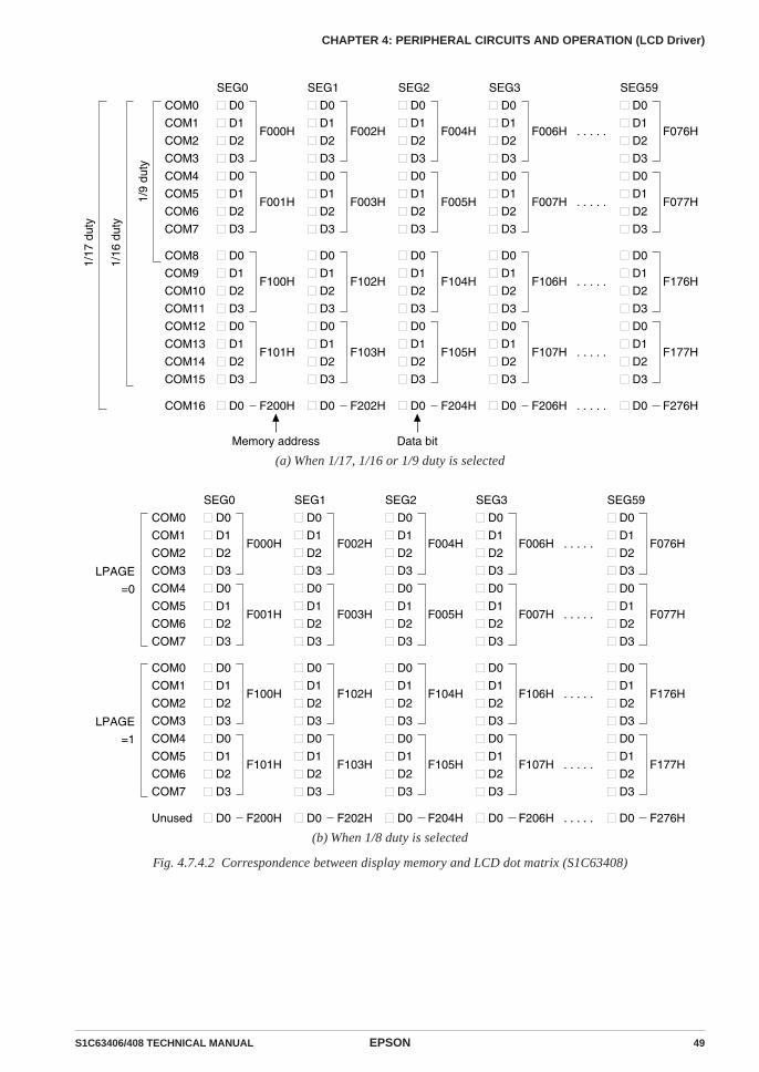
S1C63406/408 TECHNICAL MANUAL EPSON 49
CHAPTER 4: PERIPHERAL CIRCUITS AND OPERATION (LCD Driver)
COM0
COM1
COM2
COM3
COM4
COM5
COM6
COM7
COM8
COM9
COM10
COM11
COM12
COM13
COM14
COM15
COM16
SEG0
D0
D1
D2
D3
D0
D1
D2
D3
D0
D1
D2
D3
D0
D1
D2
D3
D0
F000H
F001H
F100H
F101H
Memory address
F200H
SEG1
D0
D1
D2
D3
D0
D1
D2
D3
D0
D1
D2
D3
D0
D1
D2
D3
D0
F002H
F003H
F102H
F103H
F202H
SEG2
D0
D1
D2
D3
D0
D1
D2
D3
D0
D1
D2
D3
D0
D1
D2
D3
D0
F004H
F005H
F104H
F105H
F204H
SEG3
D0
D1
D2
D3
D0
D1
D2
D3
D0
D1
D2
D3
D0
D1
D2
D3
D0
F006H
F007H
F106H
F107H
F206H
. . . . .
. . . . .
. . . . .
. . . . .
. . . . .
SEG59
D0
D1
D2
D3
D0
D1
D2
D3
D0
D1
D2
D3
D0
D1
D2
D3
D0
F076H
F077H
F176H
F177H
F276H
1/16
dut
y
1/17
dut
y
1/9
duty
Data bit
(a) When 1/17, 1/16 or 1/9 duty is selected
COM0
COM1
COM2
COM3
COM4
COM5
COM6
COM7
COM0
COM1
COM2
COM3
COM4
COM5
COM6
COM7
Unused
SEG0
D0
D1
D2
D3
D0
D1
D2
D3
D0
D1
D2
D3
D0
D1
D2
D3
D0
F000H
LPAGE
=0
LPAGE
=1
F001H
F100H
F101H
F200H
SEG1
D0
D1
D2
D3
D0
D1
D2
D3
D0
D1
D2
D3
D0
D1
D2
D3
D0
F002H
F003H
F102H
F103H
F202H
SEG2
D0
D1
D2
D3
D0
D1
D2
D3
D0
D1
D2
D3
D0
D1
D2
D3
D0
F004H
F005H
F104H
F105H
F204H
SEG3
D0
D1
D2
D3
D0
D1
D2
D3
D0
D1
D2
D3
D0
D1
D2
D3
D0
F006H
F007H
F106H
F107H
F206H
. . . . .
. . . . .
. . . . .
. . . . .
. . . . .
SEG59
D0
D1
D2
D3
D0
D1
D2
D3
D0
D1
D2
D3
D0
D1
D2
D3
D0
F076H
F077H
F176H
F177H
F276H
(b) When 1/8 duty is selected
Fig. 4.7.4.2 Correspondence between display memory and LCD dot matrix (S1C63408)

50 EPSON S1C63406/408 TECHNICAL MANUAL
CHAPTER 4: PERIPHERAL CIRCUITS AND OPERATION (LCD Driver)
4.7.5 LCD contrast adjustmentIn the S1C63406/408, the LCD contrast can be adjusted by the software.It is realized by controlling the voltages VC1–VC5 output from the LCD system voltage circuit. Thecontrast can be adjusted to 16 levels as shown in Table 4.7.5.1. When VCCHG = "0", VC1 is changed withinthe range from 0.975 V to 1.2 V, and other voltages change according to VC1. When VCCHG = "1", VC2 ischanged within the range from 1.950 V to 2.4 V, and other voltages change according to VC2.
Table 4.7.5.1 LCD contrastNo.
0
1
2
3
4
5
6
7
8
9
10
11
12
13
14
15
LC3
0
0
0
0
0
0
0
0
1
1
1
1
1
1
1
1
LC2
0
0
0
0
1
1
1
1
0
0
0
0
1
1
1
1
LC1
0
0
1
1
0
0
1
1
0
0
1
1
0
0
1
1
LC0
0
1
0
1
0
1
0
1
0
1
0
1
0
1
0
1
Contrast
light
dark
At room temperature, use setting number 7 or 8 as standard.Since the contents of LC0–LC3 are undefined at initial reset, initialize it by the software.

S1C63406/408 TECHNICAL MANUAL EPSON 51
CHAPTER 4: PERIPHERAL CIRCUITS AND OPERATION (LCD Driver)
4.7.6 I/O memory of LCD driverTable 4.7.6.1 shows the I/O addresses and the control bits for the LCD driver. Figures 4.7.6.1and 4.7.6.2show the display memory maps of the S1C63406 and S1C63408, respectively.
Table 4.7.6.1 LCD driver control bits
Address CommentD3 D2
Register
D1 D0 Name Init ∗ 1 1 0
0Light
––
15Dark
[LC3–0]Contrast
FF62HLC3 LC2 LC1 LC0
R/W
LC3LC2LC1LC0
– ∗ 2
– ∗ 2
– ∗ 2
– ∗ 2
LCD contrast adjustment
FF61H
EXLCDC ALOFF ALON LPAGE
R/W
EXLCDCALOFFALON
LPAGE
0100
1All OffAll On
F100-F177
0NormalNormal
F000-F077
General-purpose register
LCD all OFF control
LCD all ON control
Display memory area (when 1/8 duty is selected in S1C63408)
General-purpose register for S1C63406 or when 1/17, 1/16 or
1/9 duty is selected in S1C63408
FF60HLDUTY1 LDUTY0 VCCHG LPWR
R/W
LDUTY1LDUTY0VCCHGLPWR
0000
VC2
OnVC1
Off
LCD drive
duty switch
LCD regulated voltage switch
LCD power On/Off
01/9
11/8
2 *1/17
3 *1/16
(∗ S1C63408 only)
[LDUTY1, 0]Duty
*1 Initial value at initial reset
*2 Not set in the circuit
*3 Constantly "0" when being read
F000H
F001H
F002H
F003H
F004H
:
F075H
F076H
F077H
F078H
:
F0FFH
D3
COM3
COM7
COM3
COM7
COM3
COM7
COM3
COM7
D2
COM2
COM6
COM2
COM6
COM2
COM6
COM2
COM6
D1
COM1
COM5
COM1
COM5
COM1
COM5
COM1
COM5
D0
COM0
COM4
COM0
COM4
COM0
COM4
COM0
COM4
SEG0
SEG0
SEG1
SEG1
SEG2
SEG58
SEG59
SEG59
Not-implemented
COM0—COM7
0 Unused area Always "0"
No Operation
Reading:
Writing:
F100H
F101H
F102H
F103H
:
F174H
F175H
F176H
F177H
D3
0
0
0
0
D2
0
0
0
0
D1
0
0
0
0
D0
COM8
COM8
COM8
COM8
SEG0
SEG1
SEG58
SEG59
COM8
Non-implementation area Read/write disabled
Fig. 4.7.6.1 S1C63406 display memory map
F000H
F001H
F002H
F003H
F004H
:
F075H
F076H
F077H
F078H
:
F0FFH
D3
COM3
COM7
COM3
COM7
COM3
COM7
COM3
COM7
D2
COM2
COM6
COM2
COM6
COM2
COM6
COM2
COM6
D1
COM1
COM5
COM1
COM5
COM1
COM5
COM1
COM5
D0
COM0
COM4
COM0
COM4
COM0
COM4
COM0
COM4
SEG0
SEG0
SEG1
SEG1
SEG2
SEG58
SEG59
SEG59
Not-implemented
COM0–COM7
F100H
F101H
F102H
F103H
F104H
:
F175H
F176H
F177H
F178H
:
F1FFH
D3
COM11
COM15
COM11
COM15
COM11
COM15
COM11
COM15
D2
COM10
COM14
COM10
COM14
COM10
COM14
COM10
COM14
0 Unused area Always "0"
No Operation
Reading:
Writing:
D1
COM09
COM13
COM09
COM13
COM09
COM13
COM09
COM13
D0
COM8
COM12
COM8
COM12
COM8
COM12
COM8
COM12
SEG0
SEG0
SEG1
SEG1
SEG2
SEG58
SEG59
SEG59
Not-implemented
COM8–COM15
F200H
F201H
F202H
F203H
:
F274H
F275H
F276H
F277H
D3
0
0
0
0
D2
0
0
0
0
D1
0
0
0
0
D0
COM16
COM16
COM16
COM16
SEG0
SEG1
SEG58
SEG59
COM16
Non-implementation area Read/write disabled
Fig. 4.7.6.2 S1C63408 display memory map

52 EPSON S1C63406/408 TECHNICAL MANUAL
CHAPTER 4: PERIPHERAL CIRCUITS AND OPERATION (LCD Driver)
LPWR: LCD power control (ON/OFF) register (FF60H•D0)Turns the LCD system voltage circuit ON and OFF.
When "1" is written: ONWhen "0" is written: OFF
Reading: Valid
When "1" is written to the LPWR register, the LCD system voltage circuit goes ON and generates the LCDdrive voltage. When "0" is written, all the LCD drive voltages go to VSS level.It takes about 100 msec for the LCD drive voltage to stabilize after starting up the LCD system voltagecircuit by writing "1" to the LPWR register.At initial reset, this register is set to "0".
VCCHG: LCD regulated voltage switching register (FF60H•D1)Selects the reference voltage for the LCD drive voltage.
When "1" is written: VC2
When "0" is written: VC1
Reading: Valid
When "1" is written to the VCCHG register, the LCD system voltage circuit generates the LCD drivevoltage as VC2 standard. When "0" is written, it becomes VC1 standard. Select VC2 when power supplyvoltage is 2.5 V or more, otherwise, select VC1.At initial reset, this register is set to "0".
LDUTY0, LDUTY1: LCD drive duty switching register (FF60H•D2, D3)Selects the LCD drive duty.
Table 4.7.6.2 Drive duty settingLDUTY1*
1
1
0
0
LDUTY0
1
0
1
0
Drive duty
1/16*
1/17*
1/8
1/9
Common terminal used
COM0–COM15*
COM0–COM16*
COM0–COM7
COM0–COM8
Maximum segment number
960 (60 × 16)*
1,020 (60 × 17)*
480 (60 × 8)
540 (60 × 9)∗ The S1C63406 does not support 1/16 duty or 1/17 duty. LDUTY1 functions as a
general-purpose register that does not affect the drive duty.
At initial reset, this register is set to "0".
ALON: LCD all ON control register (FF61H•D1)Displays the all LCD dots ON.
When "1" is written: All LCD dots displayedWhen "0" is written: Normal display
Reading: Valid
By writing "1" to the ALON register, all the LCD dots goes ON, and when "0" is written, it returns tonormal display.This function outputs an ON waveform to the SEG terminals, and does not affect the content of thedisplay memory.ALON has priority over ALOFF.At initial reset, this register is set to "0".

S1C63406/408 TECHNICAL MANUAL EPSON 53
CHAPTER 4: PERIPHERAL CIRCUITS AND OPERATION (LCD Driver)
ALOFF: LCD all OFF control register (FF61H•D2)Fade outs the all LCD dots.
When "1" is written: All LCD dots fade outWhen "0" is written: Normal display
Reading: Valid
By writing "1" to the ALOFF register, all the LCD dots goes OFF, and when "0" is written, it returns tonormal display.This function outputs an OFF waveform to the SEG terminals, and does not affect the content of thedisplay memory.At initial reset, this register is set to "1".
LPAGE: LCD display memory selection register (FF61H•D0)Selects the display memory area at 1/8 duty drive. (S1C63408 only)
When "1" is written: F100H–F177HWhen "0" is written: F000H–F077H
Reading: Valid
By writing "1" to the LPAGE register, the data set in F100H–F177H (the second half of the displaymemory) is displayed, and when "0" is written, the data set in F000H–F077H (the first half of the displaymemory) is displayed.This function is valid only when 1/8 duty is selected in the S1C63408, and when 1/9, 1/16 or 1/17 duty isselected, or in the S1C63406, this register can be used as a general purpose register.At initial reset, this register is set to "0".
LC3–LC0: LCD contrast adjustment register (FF62H)Adjusts the LCD contrast.
LC3–LC0 = 0000B light: :
LC3–LC0 = 1111B dark
At room temperature, use setting number 7 or 8 as standard.At initial reset, LC0–LC3 are undefined.
4.7.7 Programming notes(1) Current consumption will be increased for a cycle of 1 kHz to stabilize the LCD power quickly after
setting LPWR on.
(2) When a program that access no memory mounted area shown below is made, the operation is notguaranteed.S1C63406: F078H–F0FFH, F101H, F103H, · · ·, F177HS1C63408: F078H–F0FFH, F178H–F1FFH, F201H, F203H, · · ·, F277H
(3) Because at initial reset, the contents of display memory and LC3–LC0 (LCD contrast) are undefined,there is need to initialize by the software. Furthermore, take care of the registers LPWR and ALOFFbecause these are set so that the display goes OFF.

54 EPSON S1C63406/408 TECHNICAL MANUAL
CHAPTER 4: PERIPHERAL CIRCUITS AND OPERATION (Clock Timer)
4.8 Clock Timer
4.8.1 Configuration of clock timerThe S1C63406/408 has a built-in clock timer that uses OSC1 (crystal oscillator) as the source oscillator.The clock timer is configured of an 8-bit binary counter that serves as the input clock, fOSC1 divided clockoutput from the prescaler. Timer data (128–16 Hz and 8–1 Hz) can be read out by the software.Figure 4.8.1.1 is the block diagram for the clock timer.
128 Hz–16 Hz
Data bus
32 Hz, 8 Hz, 2 Hz, 1 Hz
256 Hz
Clock timer reset signal
Divider
Interruptrequest
Interruptcontrol
8 Hz–1 Hz
Clock timer RUN/STOP signal
Clock timerOSC1oscillation circuit(fOSC1)
Fig. 4.8.1.1 Block diagram for the clock timer
Ordinarily, this clock timer is used for all types of timing functions such as clocks.
Note: When the CR oscillation circuit is selected as the OSC1 oscillation circuit by mask option, thefrequencies and times differ from the values described in this section because the oscillationfrequency will be 60 kHz (Typ.). Therefore, the clock timer can not be used for the clock function.
4.8.2 Data reading and hold functionThe 8 bits timer data are allocated to the address FF79H and FF7AH.
<FF79H> D0: TM0 = 128 Hz D1: TM1 = 64 Hz D2: TM2 = 32 Hz D3: TM3 = 16 Hz<FF7AH> D0: TM4 = 8 Hz D1: TM5 = 4 Hz D2: TM6 = 2 Hz D3: TM7 = 1 Hz
Since the clock timer data has been allocated to two addresses, a carry is generated from the low-orderdata within the count (TM0–TM3: 128–16 Hz) to the high-order data (TM4–TM7: 8–1 Hz). When this carryis generated between the reading of the low-order data and the high-order data, a content combining thetwo does not become the correct value (the low-order data is read as FFH and the high-order databecomes the value that is counted up 1 from that point).The high-order data hold function in the S1C63406/408 is designed to operate to avoid this. This functiontemporarily stops the counting up of the high-order data (by carry from the low-order data) at the pointwhere the low-order data has been read and consequently the time during which the high-order data isheld is the shorter of the two indicated here following.
1. Period until it reads the high-order data.
2. 0.48–1.5 msec (Varies due to the read timing.)
Note: Since the low-order data is not held when the high-order data has previously been read, the low-order data should be read first.
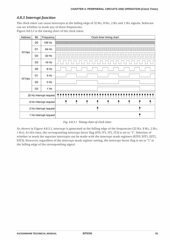
S1C63406/408 TECHNICAL MANUAL EPSON 55
CHAPTER 4: PERIPHERAL CIRCUITS AND OPERATION (Clock Timer)
4.8.3 Interrupt functionThe clock timer can cause interrupts at the falling edge of 32 Hz, 8 Hz, 2 Hz and 1 Hz signals. Softwarecan set whether to mask any of these frequencies.Figure 4.8.3.1 is the timing chart of the clock timer.
Address
FF79H
FF7AH
32 Hz interrupt request
8 Hz interrupt request
2 Hz interrupt request
1 Hz interrupt request
Bit
D0
D1
D2
D3
D0
D1
D2
D3
Frequency Clock timer timing chart
128 Hz
64 Hz
32 Hz
16 Hz
8 Hz
4 Hz
2 Hz
1 Hz
Fig. 4.8.3.1 Timing chart of clock timer
As shown in Figure 4.8.3.1, interrupt is generated at the falling edge of the frequencies (32 Hz, 8 Hz, 2 Hz,1 Hz). At this time, the corresponding interrupt factor flag (IT0, IT1, IT2, IT3) is set to "1". Selection ofwhether to mask the separate interrupts can be made with the interrupt mask registers (EIT0, EIT1, EIT2,EIT3). However, regardless of the interrupt mask register setting, the interrupt factor flag is set to "1" atthe falling edge of the corresponding signal.

56 EPSON S1C63406/408 TECHNICAL MANUAL
CHAPTER 4: PERIPHERAL CIRCUITS AND OPERATION (Clock Timer)
4.8.4 I/O memory of clock timerTable 4.8.4.1 shows the I/O addresses and the control bits for the clock timer.
Table 4.8.4.1 Control bits of clock timer
Address CommentD3 D2
Register
D1 D0 Name Init ∗1 1 0
W R/WR
FF78H0 0 TMRST TMRUN
0 ∗3
0 ∗3
TMRST∗3
TMRUN
– ∗2
– ∗2
Reset0
ResetRun
InvalidStop
Unused
Unused
Clock timer reset (writing)
Clock timer Run/Stop
R
FF79HTM3 TM2 TM1 TM0
TM3TM2TM1TM0
0000
Clock timer data (16 Hz)
Clock timer data (32 Hz)
Clock timer data (64 Hz)
Clock timer data (128 Hz)
R
FF7AHTM7 TM6 TM5 TM4
TM7TM6TM5TM4
0000
Clock timer data (1 Hz)
Clock timer data (2 Hz)
Clock timer data (4 Hz)
Clock timer data (8 Hz)
FFE6HEIT3 EIT2 EIT1 EIT0
R/W
EIT3EIT2EIT1EIT0
0000
EnableEnableEnableEnable
MaskMaskMaskMask
Interrupt mask register (Clock timer 1 Hz)
Interrupt mask register (Clock timer 2 Hz)
Interrupt mask register (Clock timer 8 Hz)
Interrupt mask register (Clock timer 32 Hz)
FFF6HIT3 IT2 IT1 IT0
R/W
IT3IT2IT1IT0
0000
(R)Yes(W)
Reset
(R)No(W)
Invalid
Interrupt factor flag (Clock timer 1 Hz)
Interrupt factor flag (Clock timer 2 Hz)
Interrupt factor flag (Clock timer 8 Hz)
Interrupt factor flag (Clock timer 32 Hz)
*1 Initial value at initial reset
*2 Not set in the circuit
*3 Constantly "0" when being read
TM0–TM7: Timer data (FF79H, FF7AH)The 128–1 Hz timer data of the clock timer can be read out with these registers. These eight bits are readonly, and writing operations are invalid.By reading the low-order data (FF79H), the high-order data (FF7AH) is held until reading or for 0.48–1.5msec (one of shorter of them).At initial reset, the timer data is initialized to "00H".
TMRST: Clock timer reset (FF78H•D1)This bit resets the clock timer.
When "1" is written: Clock timer resetWhen "0" is written: No operation
Reading: Always "0"
The clock timer is reset by writing "1" to TMRST. When the clock timer is reset in the RUN status, opera-tion restarts immediately. Also, in the STOP status the reset data is maintained. No operation resultswhen "0" is written to TMRST.This bit is write-only, and so is always "0" at reading.
S1C63406/408 TECHNICAL MANUAL EPSON 57
CHAPTER 4: PERIPHERAL CIRCUITS AND OPERATION (Clock Timer)
TMRUN: Clock timer RUN/STOP control register (FF78H•D0)Controls RUN/STOP of the clock timer.
When "1" is written: RUNWhen "0" is written: STOP
Reading: Valid
The clock timer enters the RUN status when "1" is written to the TMRUN register, and the STOP statuswhen "0" is written.In the STOP status, the timer data is maintained until the next RUN status or the timer is reset. Also,when the STOP status changes to the RUN status, the data that is maintained can be used for resumingthe count.At initial reset, this register is set to "0".
EIT0: 32 Hz interrupt mask register (FFE6H•D0)EIT1: 8 Hz interrupt mask register (FFE6H•D1)EIT2: 2 Hz interrupt mask register (FFE6H•D2)EIT3: 1 Hz interrupt mask register (FFE6H•D3)These registers are used to select whether to mask the clock timer interrupt.
When "1" is written: EnabledWhen "0" is written: Masked
Reading: Valid
The interrupt mask registers (EIT0, EIT1, EIT2, EIT3) are used to select whether to mask the interrupt tothe separate frequencies (32 Hz, 8 Hz, 2 Hz, 1 Hz).At initial reset, these registers are set to "0".
IT0: 32 Hz interrupt factor flag (FFF6H•D0)IT1: 8 Hz interrupt factor flag (FFF6H•D1)IT2: 2 Hz interrupt factor flag (FFF6H•D2)IT3: 1 Hz interrupt factor flag (FFF6H•D3)These flags indicate the status of the clock timer interrupt.
When "1" is read: Interrupt has occurredWhen "0" is read: Interrupt has not occurred
When "1" is written: Flag is resetWhen "0" is written: Invalid
The interrupt factor flags (IT0, IT1, IT2, IT3) correspond to the clock timer interrupts of the respectivefrequencies (32 Hz, 8 Hz, 2 Hz, 1 Hz). The software can judge from these flags whether there is a clocktimer interrupt. However, even if the interrupt is masked, the flags are set to "1" at the falling edge of thesignal.These flags are reset to "0" by writing "1" to them.After an interrupt occurs, the same interrupt will occur again if the interrupt enabled state (I flag = "1") isset or the RETI instruction is executed unless the interrupt factor flag is reset. Therefore, be sure to reset(write "1" to) the interrupt factor flag in the interrupt service routine before shifting to the interruptenabled state.At initial reset, these flags are set to "0".
58 EPSON S1C63406/408 TECHNICAL MANUAL
CHAPTER 4: PERIPHERAL CIRCUITS AND OPERATION (Clock Timer)
4.8.5 Programming notes(1) Be sure to read timer data in the order of low-order data (TM0–TM3) then high-order data (TM4–
TM7).
(2) After an interrupt occurs, the same interrupt will occur again if the interrupt enabled state (I flag ="1") is set or the RETI instruction is executed unless the interrupt factor flag is reset. Therefore, be sureto reset (write "1" to) the interrupt factor flag in the interrupt service routine before shifting to theinterrupt enabled state.
(3) When the CR oscillation circuit is selected as the OSC1 oscillation circuit by mask option, the frequen-cies and times differ from the values described in this section because the oscillation frequency will be60 kHz (Typ.). Therefore, the clock timer can not be used for the clock function.

S1C63406/408 TECHNICAL MANUAL EPSON 59
CHAPTER 4: PERIPHERAL CIRCUITS AND OPERATION (Stopwatch Timer)
4.9 Stopwatch Timer
4.9.1 Configuration of stopwatch timerThe S1C63406/408 has 1/100 sec unit and 1/10 sec unit stopwatch timer built-in. The stopwatch timer isconfigured with a 2 levels 4-bit BCD counter which has an input clock approximating 100 Hz signal(signal divided from OSC1 to the closest 100 Hz) and data can be read in units of 4 bits by software.Figure 4.9.1.1 shows the configuration of the stopwatch timer.
SWD0–3
Data bus
10 Hz, 1 Hz
256 Hz 10 Hz
Stopwatch timer reset signal
Divider
Interruptrequest
Interruptcontrol
SWD4–7
Stopwatch timer RUN/STOP signal
Stopwatch timerOSC1oscillation circuit(fOSC1)
Fig. 4.9.1.1 Configuration of stopwatch timer
The stopwatch timer can be used as a separate timer from the clock timer. In particular, digital watchstopwatch functions can be realized easily with software.
Note: When the CR oscillation circuit is selected as the OSC1 oscillation circuit by mask option, thefrequencies and times differ from the values described in this section because the oscillationfrequency will be 60 kHz (Typ.). Therefore, this timer can not be used for the stopwatch function.
4.9.2 Count-up patternThe stopwatch timer is configured of 4-bit BCD counters SWD0–SWD3 and SWD4–SWD7.The counter SWD0–SWD3, at the stage preceding the stopwatch timer, has an approximated 100 Hzsignal for the input clock. It counts up every 1/100 sec, and generates an approximated 10 Hz signal. Thecounter SWD4–SWD7 has an approximated 10 Hz signal generated by the counter SWD0–SWD3 for theinput clock. In count-up every 1/10 sec, and generated 1 Hz signal.Figure 4.9.2.1 shows the count-up pattern of the stopwatch timer.
26256
26256
26256
26256
26256
26256
25256
25256
25256
25256
3256
2256
3256
2256
2256
2256
3256
3256
3256
2256
3256
2256
3256
3256
3256
3256
3256
2256
2256
2256
26256
25256
26256
25256
x 6 + x 4 = 1 (sec)
0 1 2 3 4 5 6 7 8 9 0
0 1 2 3 4 5 6 7 8 9 0
0 1 2 3 4 5 6 7 8 9 0
1 Hzsignalgeneration
Approximate10 Hzsignalgeneration
Approximate10 Hzsignalgeneration
SWD4–7 count value
Counting time (sec)
(sec)
(sec)
SWD0–3 count value
Counting time (sec)
SWD0–3 count value
Counting time (sec)
SWD4–7 count-up pattern
SWD0–3 count-up pattern 1
SWD0–3 count-up pattern 2
Fig. 4.9.2.1 Count-up pattern of stopwatch timer

60 EPSON S1C63406/408 TECHNICAL MANUAL
CHAPTER 4: PERIPHERAL CIRCUITS AND OPERATION (Stopwatch Timer)
SWD0–SWD3 generates an approximated 10 Hz signal from the basic 256 Hz signal (fOSC1 dividingclock). The count-up intervals are 2/256 sec and 3/256 sec, so that finally two patterns are generated: 25/256 sec and 26/256 sec intervals. Consequently, these patterns do not amount to an accurate 1/100 sec.SWD4–SWD7 counts the approximated 10 Hz signals generated by the 25/256 sec and 26/256 sec inter-vals in the ratio of 4 : 6, to generate a 1 Hz signal. The count-up intervals are 25/256 sec and 26/256 sec,which do not amount to an accurate 1/10 sec.
4.9.3 Interrupt functionThe stopwatch timers SWD0–SWD3 and SWD4–SWD7, through their respective overflows, can generate10 Hz (approximate 10 Hz) and 1 Hz interrupts.Figure 4.9.3.1 shows the timing chart for the stopwatch timer.
Address
FF7DH1/100sec
(BCD)
10 Hz Interrupt request
Bit
D0
D1
D2
D3
Stopwatch timer (SWD0–3) timing chart
Address
FF7EH1/10sec(BCD)
1 Hz Interrupt request
Bit
D0
D1
D2
D3
Stopwatch timer (SWD4–7) timing chart
Fig. 4.9.3.1 Timing chart for stopwatch timer
The stopwatch interrupts are generated by the overflow of their respective counters SWD0–SWD3 andSWD4–SWD7 (changing "9" to "0"). At this time, the corresponding interrupt factor flags (ISW10 andISW1) are set to "1".The respective interrupts can be masked separately using the interrupt mask registers (EISW10 andEISW1). However, regardless of the setting of the interrupt mask registers, the interrupt factor flags areset to "1" by the overflow of their corresponding counters.

S1C63406/408 TECHNICAL MANUAL EPSON 61
CHAPTER 4: PERIPHERAL CIRCUITS AND OPERATION (Stopwatch Timer)
4.9.4 I/O memory of stopwatch timerTable 4.9.4.1 shows the I/O addresses and the control bits for the stopwatch timer.
Table 4.9.4.1 Control bits of stopwatch timer
Address CommentD3 D2
Register
D1 D0 Name Init ∗1 1 0
W R/WR
FF7CH0 0 SWRST SWRUN
0 ∗3
0 ∗3
SWRST∗3
SWRUN
– ∗2
– ∗2
Reset0
ResetRun
InvalidStop
Unused
Unused
Stopwatch timer reset (writing)
Stopwatch timer Run/Stop
R
FF7DHSWD3 SWD2 SWD1 SWD0
SWD3SWD2SWD1SWD0
0000
Stopwatch timer data
BCD (1/100 sec)
SWD7SWD6SWD5SWD4
0000
Stopwatch timer data
BCD (1/10 sec)R
FF7EHSWD7 SWD6 SWD5 SWD4
FFF7H0 0 ISW1 ISW10
R R/W
0 ∗3
0 ∗3
ISW1ISW10
– ∗2
– ∗2
00
(R)Yes(W)
Reset
(R)No(W)
Invalid
Unused
Unused
Interrupt factor flag (Stopwatch timer 1 Hz)
Interrupt factor flag (Stopwatch timer 10 Hz)
FFE7HGPR73 GPR72 EISW1 EISW10
R/W
GPR73GPR72EISW1EISW10
0000
11
EnableEnable
00
MaskMask
General-purpose register
General-purpose register
Interrupt mask register (Stopwatch timer 1 Hz)
Interrupt mask register (Stopwatch timer 10 Hz)
*1 Initial value at initial reset
*2 Not set in the circuit
*3 Constantly "0" when being read
SWD0–SWD7: Stopwatch timer data (FF7DH, FF7EH)The 1/100 sec and the 1/10 sec data (BCD) can be read from SWD0–SWD3 and SWD4–SWD7, respec-tively. These eight bits are read only, and writing operations are invalid.At initial reset, the timer data is initialized to "00H".
SWRST: Stopwatch timer reset (FF7CH•D1)
When "1" is written: Stopwatch timer resetWhen "0" is written: No operation
Reading: Always "0"
The stopwatch timer is reset by writing "1" to SWRST. All timer data is set to "0". When the stopwatchtimer is reset in the RUN status, operation restarts immediately. Also, in the STOP status the reset data ismaintained. No operation results when "0" is written to SWRST.This bit is write-only, and so is always "0" at reading.
SWRUN: Stopwatch timer RUN/STOP control register (FF7CH•D0)Controls RUN/STOP of the stopwatch timer.
When "1" is written: RUNWhen "0" is written: STOP
Reading: Valid
The stopwatch timer enters the RUN status when "1" is written to the SWRUN register, and the STOPstatus when "0" is written.In the STOP status, the timer data is maintained until the next RUN status or the timer is reset. Also,when the STOP status changes to the RUN status, the data that is maintained can be used for resumingthe count.
62 EPSON S1C63406/408 TECHNICAL MANUAL
CHAPTER 4: PERIPHERAL CIRCUITS AND OPERATION (Stopwatch Timer)
When data of the counter is read at run mode, proper reading may not be obtained due to the carry fromlow-order digits (SWD0–SWD3) into high-order digits (SWD4–SWD7) (i.e., in case SWD0–SWD3 andSWD4–SWD7 reading span the timing of the carry). To avoid this occurrence, perform the reading aftersuspending the counter once and then set the SWRUN to "1" again.Moreover, it is required that the suspension period not exceed 976 µsec (1/4 cycle of 256 Hz).At initial reset, this register is set to "0".
EISW10: 10Hz interrupt mask register (FFE7H•D0)EISW1: 1Hz interrupt mask register (FFE7H•D1)These registers are used to select whether to mask the stopwatch timer interrupt.
When "1" is written: EnabledWhen "0" is written: Masked
Reading: Valid
The interrupt mask registers (EISW10, EISW1) are used to select whether to mask the interrupt to theseparate frequencies (10 Hz, 1 Hz).At initial reset, these registers are set to "0".
ISW10: 10 Hz interrupt factor flag (FFF7H•D0)ISW1: 1 Hz interrupt factor flag (FFF7H•D1)These flags indicate the status of the stopwatch timer interrupt.
When "1" is read: Interrupt has occurredWhen "0" is read: Interrupt has not occurred
When "1" is written: Flag is resetWhen "0" is written: Invalid
The interrupt factor flags ISW10 and ISW1 correspond to 10 Hz and 1 Hz stopwatch timer interrupts,respectively. The software can judge from these flags whether there is a stopwatch timer interrupt.However, even if the interrupt is masked, the flags are set to "1" by the overflow of the correspondingcounters.These flags are reset to "0" by writing "1" to them.After an interrupt occurs, the same interrupt will occur again if the interrupt enabled state (I flag = "1") isset or the RETI instruction is executed unless the interrupt factor flag is reset. Therefore, be sure to reset(write "1" to) the interrupt factor flag in the interrupt service routine before shifting to the interruptenabled state.At initial reset, these flags are set to "0".
4.9.5 Programming notes(1) When data of the counter is read at run mode, perform the reading after suspending the counter once
and then set SWRUN to "1" again. Moreover, it is required that the suspension period not exceed 976µsec (1/4 cycle of 256 Hz).
(2) After an interrupt occurs, the same interrupt will occur again if the interrupt enabled state (I flag ="1") is set or the RETI instruction is executed unless the interrupt factor flag is reset. Therefore, be sureto reset (write "1" to) the interrupt factor flag in the interrupt service routine before shifting to theinterrupt enabled state.
(3) When the CR oscillation circuit is selected as the OSC1 oscillation circuit by mask option, the frequen-cies and times differ from the values described in this section because the oscillation frequency will be60 kHz (Typ.). Therefore, this timer can not be used for the stopwatch function.
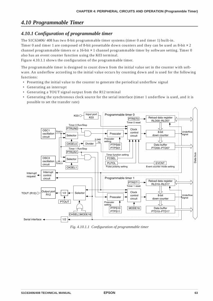
S1C63406/408 TECHNICAL MANUAL EPSON 63
CHAPTER 4: PERIPHERAL CIRCUITS AND OPERATION (Programmble Timer)
4.10 Programmable Timer
4.10.1 Configuration of programmable timerThe S1C63406/408 has two 8-bit programmable timer systems (timer 0 and timer 1) built-in.Timer 0 and timer 1 are composed of 8-bit presettable down counters and they can be used as 8-bit × 2channel programmable timers or a 16-bit × 1 channel programmable timer by software setting. Timer 0also has an event counter function using the K03 terminal.Figure 4.10.1.1 shows the configuration of the programmable timer.
The programmable timer is designed to count down from the initial value set in the counter with soft-ware. An underflow according to the initial value occurs by counting down and is used for the followingfunctions: • Presetting the initial value to the counter to generate the periodical underflow signal • Generating an interrupt • Generating a TOUT signal output from the R12 terminal • Generating the synchronous clock source for the serial interface (timer 1 underflow is used, and it is
possible to set the transfer rate)
Reload data registerRLD00–RLD07
Data bufferPTD00–PTD07
Input portK03
PTRUN0
FCSEL
PLPOL
Programmable timer 0
PTPS00PTPS01
8-bitdown counterPrescaler
Selector
CKSEL0
Timer 0 Run/Stop
K03
Clockcontrolcircuit
EVCNTEvent counter mode setting
Timer function setting
Pulse polarity setting
Prescalersetting
Underflowsignal
Data bufferPTD10–PTD17
Programmable timer 1
PTPS10PTPS11
8-bitdown counterPrescaler
Clockcontrolcircuit
Prescalersetting
Underflowsignal
Dat
a bu
s
Interruptrequest
CHSEL
TOUT (R12)
Serial interface
Selector
CKSEL1
Timer 1 Run/Stop
PTRST0Timer 0 reset
PTRST1Timer 1 reset
2,048Hz
Divider
OSC3oscillationcircuit
Interruptcontrolcircuit
OSC1oscillationcircuit
fOSC3
fOSC1
PTRUN1
1/2
PTOUT
SelectorOutput portR12
Reload data registerRLD10–RLD17
1/2
MODE16
MODE16
Fig. 4.10.1.1 Configuration of programmable timer

64 EPSON S1C63406/408 TECHNICAL MANUAL
CHAPTER 4: PERIPHERAL CIRCUITS AND OPERATION (Programmble Timer)
4.10.2 Tow separate 8-bit timer (MODE16 = "0") operation
4.10.2.1 Setting of initial value and counting downTimers 0 and 1 each have a down counter and reload data register.
The reload data registers RLD00–RLD07 (timer 0) and RLD10–RLD17 (timer 1) are used to set the initialvalue to the down counter.By writing "1" to the timer reset bit PTRST0 (timer 0) or PTRST1 (timer 1), the down counter loads theinitial value set in the reload register RLD. Therefore, down-counting is executed from the stored initialvalue by the input clock.
The registers PTRUN0 (timer 0) and PTRUN1 (timer 1) are provided to control the RUN/STOP for timers0 and 1. By writing "1" to the register after presetting the reload data to the down counter, the downcounter starts counting down. Writing "0" stops the input count clock and the down counter stopscounting. This control (RUN/STOP) does not affect the counter data. The counter maintains its datawhile stopped, and can restart counting continuing from that data.
The counter data can be read via the data buffers PTD00–PTD07 (timer 0) and PTD10–PTD17 (timer 1) inoptional timing. However, the counter has the data hold function the same as the clock timer, that holdsthe high-order data when the low-order data is read in order to prevent the borrowing operation betweenlow- and high-order reading, therefore be sure to read the low-order data first.
The counter reloads the initial value set in the reload data register RLD when an underflow occursthrough the count down. It continues counting down from the initial value after reloading.In addition to reloading the counter, this underflow signal controls the interrupt generation, pulse (TOUTsignal) output and clock supplying to the serial interface.
PTRUN0 (1)
PTRST0 (1)
RLD00–07 (10–17)
Input clock
PTD07 (17)
PTD06 (16)
PTD05 (15)
PTD04 (14)
PTD03 (13)
PTD02 (12)
PTD01 (11)
PTD00 (10)
A6H F3H
Preset Reload &Interrupt generation
Fig. 4.10.2.1.1 Basic operation timing of down counter

S1C63406/408 TECHNICAL MANUAL EPSON 65
CHAPTER 4: PERIPHERAL CIRCUITS AND OPERATION (Programmble Timer)
4.10.2.2 Counter modeThe programmable timer can operate in two counter modes, timer mode and event counter mode. It canbe selected by software.
(1) Timer modeThe timer mode counts down using the prescaler output as an input clock. In this mode, the program-mable timer operates as a periodical timer using the OSC1 or OSC3 oscillation clock as a clock source.Timer 0 can operate in both the timer mode and the event counter mode. The mode can be switchedusing the timer 0 counter mode selection register EVCNT. When the EVCNT register is set to "0",timer 0 operates in the timer mode.Timer 1 operates only in the timer mode.At initial reset, this mode is set.
Refer to Section 4.10.2.1, "Setting of initial value and counting down" for basic operation and control.
The input clock in the timer mode is generated by the prescaler built into the programmable timer.The prescaler generates the input clock by dividing the OSC1 or OSC3 oscillation clock. Refer to thenext section for setting the input clock.
(2) Event counter modeThe timer 0 has an event counter function that counts an external clock input to the I/O port K03. Thisfunction is selected by writing "1" to the timer 0 counter mode selection register EVCNT. The timer 1operates only in the timer mode, and cannot be used as an event counter.
In the event counter mode, the clock is supplied to timer 0 from outside of the IC, therefore, thesettings of the timer 0 prescaler division ratio selection registers PTPS00 and PTPS01 and the settingsof the timer 0 source clock selection register CKSEL0 become invalid.
Count down timing can be selected from either the falling or rising edge of the input clock using thetimer 0 pulse polarity selection register PLPOL. When "0" is written to the PLPOL register, the fallingedge is selected, and when "1" is written, the rising edge is selected. The count down timing is shownin Figure 4.10.2.2.1.
K03 input
Count data n n-1 n-2 n-3 n-4 n-5 n-6
PLPOL
EVCNT
0 1
1
PTRUN0
Fig. 4.10.2.2.1 Timing chart in event counter mode
The event counter mode also includes a noise reject function to eliminate noise such as chattering onthe external clock (K03 input signal). This function is selected by writing "1" to the timer 0 functionselection register FCSEL.When "with noise rejector" is selected, an input pulse width for both low and high levels must be 0.98msec or more to count reliably. (The noise rejecter allows the counter to input the clock at the secondfalling edge of the internal 2,048 Hz signal after changing the input level of the K03 terminal. Conse-quently, the pulse width of noise that can reliably be rejected is 0.48 msec or less.)Figure 4.10.2.2.2 shows the count down timing with noise rejecter.

66 EPSON S1C63406/408 TECHNICAL MANUAL
CHAPTER 4: PERIPHERAL CIRCUITS AND OPERATION (Programmble Timer)
Counterinput clock
Counter data n n-1 n-2 n-3
K03 input
2,048 Hz
When PLPOL register is set to "0"
Fig. 4.10.2.2.2 Count down timing with noise rejecter
The operation of the event counter mode is the same as the timer mode except it uses the K03 input asthe clock.Refer to Section 4.10.2.1, "Setting of initial value and counting down" for basic operation and control.
4.10.2.3 Setting of input clock in timer modeTimer 0 and timer 1 each include a prescaler. The prescalers generate the input clock for each timer bydividing the source clock supplied from the OSC1 or OSC3 oscillation circuit.The source clock (OSC1 or OSC3) and the division ratio of the prescaler can be selected with software fortimer 0 and timer 1 individually.The set input clock is used for the count clock during operation in the timer mode. When the timer 0 isused in the event counter mode, the following settings become invalid.
The input clock is set in the following sequence.
(1) Selection of source clockSelect the source clock input to each prescaler from either OSC1 or OSC3. This selection is done usingthe source clock selection registers CKSEL0 (timer 0) and CKSEL1 (timer 1); when "0" is written to theregister, OSC1 is selected and when "1" is written, OSC3 is selected.When the OSC3 oscillation clock is selected for the clock source, it is necessary to turn the OSC3oscillation ON, prior to using the programmable timer. However the OSC3 oscillation circuit requiresa time interval of several msec to several 10 msec from turning the circuit ON until the oscillationstabilizes. Therefore, allow an adequate interval from turning the OSC3 oscillation circuit ON tostarting the programmable timer. Refer to Section 4.3, "Oscillation Circuit", for the control and notes ofthe OSC3 oscillation circuit.At initial reset, the OSC3 oscillation circuit is set in the OFF state.
(2) Selection of prescaler division ratioSelect the division ratio for each prescaler from among 4 types. This selection is done using theprescaler division ratio selection registers PTPS00/PTPS01 (timer 0) and PTPS10/PTPS11 (timer 1).Table 4.10.2.3.1 shows the correspondence between the setting value and the division ratio.
Table 4.10.2.3.1 Selection of prescaler division ratio
PTPS11
PTPS01
1
1
0
0
PTPS10
PTPS00
1
0
1
0
Prescaler division ratio
Source clock / 256
Source clock / 32
Source clock / 4
Source clock / 1
By writing "1" to the register PTRUN0 (timer 0) or PTRUN1 (timer 1), the prescaler inputs the sourceclock and outputs the clock divided by the selected division ratio. The counter starts counting downby inputting the clock.
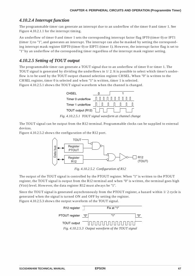
S1C63406/408 TECHNICAL MANUAL EPSON 67
CHAPTER 4: PERIPHERAL CIRCUITS AND OPERATION (Programmble Timer)
4.10.2.4 Interrupt functionThe programmable timer can generate an interrupt due to an underflow of the timer 0 and timer 1. SeeFigure 4.10.2.1.1 for the interrupt timing.
An underflow of timer 0 and timer 1 sets the corresponding interrupt factor flag IPT0 (timer 0) or IPT1(timer 1) to "1", and generates an interrupt. The interrupt can also be masked by setting the correspond-ing interrupt mask register EIPT0 (timer 0) or EIPT1 (timer 1). However, the interrupt factor flag is set to"1" by an underflow of the corresponding timer regardless of the interrupt mask register setting.
4.10.2.5 Setting of TOUT outputThe programmable timer can generate a TOUT signal due to an underflow of timer 0 or timer 1. TheTOUT signal is generated by dividing the underflows in 1/2. It is possible to select which timer's under-flow is to be used by the TOUT output channel selection register CHSEL. When "0" is written to theCHSEL register, timer 0 is selected and when "1" is written, timer 1 is selected.Figure 4.10.2.5.1 shows the TOUT signal waveform when the channel is changed.
Timer 0 underflow
Timer 1 underflow
CHSEL 0 1
TOUT output (R12)
Fig. 4.10.2.5.1 TOUT signal waveform at channel change
The TOUT signal can be output from the R12 terminal. Programmable clocks can be supplied to externaldevices.Figure 4.10.2.5.2 shows the configuration of the R12 port.
Dat
a bu
s RegisterPTOUT
RegisterR12
TOUT
R12(TOUT)
Fig. 4.10.2.5.2 Configuration of R12
The output of the TOUT signal is controlled by the PTOUT register. When "1" is written to the PTOUTregister, the TOUT signal is output from the R12 terminal and when "0" is written, the terminal goes high(VDD) level. However, the data register R12 must always be "1".
Since the TOUT signal is generated asynchronously from the PTOUT register, a hazard within 1/2 cycle isgenerated when the signal is turned ON and OFF by setting the register.Figure 4.10.2.5.3 shows the output waveform of the TOUT signal.
R12 register
PTOUT register
TOUT output
Fix at "1"
"1""0" "0"
Fig. 4.10.2.5.3 Output waveform of the TOUT signal
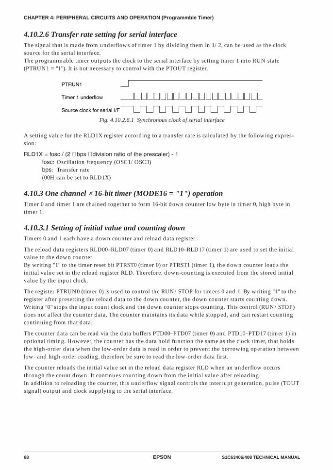
68 EPSON S1C63406/408 TECHNICAL MANUAL
CHAPTER 4: PERIPHERAL CIRCUITS AND OPERATION (Programmble Timer)
4.10.2.6 Transfer rate setting for serial interfaceThe signal that is made from underflows of timer 1 by dividing them in 1/2, can be used as the clocksource for the serial interface.The programmable timer outputs the clock to the serial interface by setting timer 1 into RUN state(PTRUN1 = "1"). It is not necessary to control with the PTOUT register.
PTRUN1
Timer 1 underflow
Source clock for serial I/F
Fig. 4.10.2.6.1 Synchronous clock of serial interface
A setting value for the RLD1X register according to a transfer rate is calculated by the following expres-sion:
RLD1X = fosc / (2 ∗ bps ∗ division ratio of the prescaler) - 1fosc: Oscillation frequency (OSC1/OSC3)bps: Transfer rate(00H can be set to RLD1X)
4.10.3 One channel × 16-bit timer (MODE16 = "1") operationTimer 0 and timer 1 are chained together to form 16-bit down counter low byte in timer 0, high byte intimer 1.
4.10.3.1 Setting of initial value and counting downTimers 0 and 1 each have a down counter and reload data register.
The reload data registers RLD00–RLD07 (timer 0) and RLD10–RLD17 (timer 1) are used to set the initialvalue to the down counter.By writing "1" to the timer reset bit PTRST0 (timer 0) or PTRST1 (timer 1), the down counter loads theinitial value set in the reload register RLD. Therefore, down-counting is executed from the stored initialvalue by the input clock.
The register PTRUN0 (timer 0) is used to control the RUN/STOP for timers 0 and 1. By writing "1" to theregister after presetting the reload data to the down counter, the down counter starts counting down.Writing "0" stops the input count clock and the down counter stops counting. This control (RUN/STOP)does not affect the counter data. The counter maintains its data while stopped, and can restart countingcontinuing from that data.
The counter data can be read via the data buffers PTD00–PTD07 (timer 0) and PTD10–PTD17 (timer 1) inoptional timing. However, the counter has the data hold function the same as the clock timer, that holdsthe high-order data when the low-order data is read in order to prevent the borrowing operation betweenlow- and high-order reading, therefore be sure to read the low-order data first.
The counter reloads the initial value set in the reload data register RLD when an underflow occursthrough the count down. It continues counting down from the initial value after reloading.In addition to reloading the counter, this underflow signal controls the interrupt generation, pulse (TOUTsignal) output and clock supplying to the serial interface.
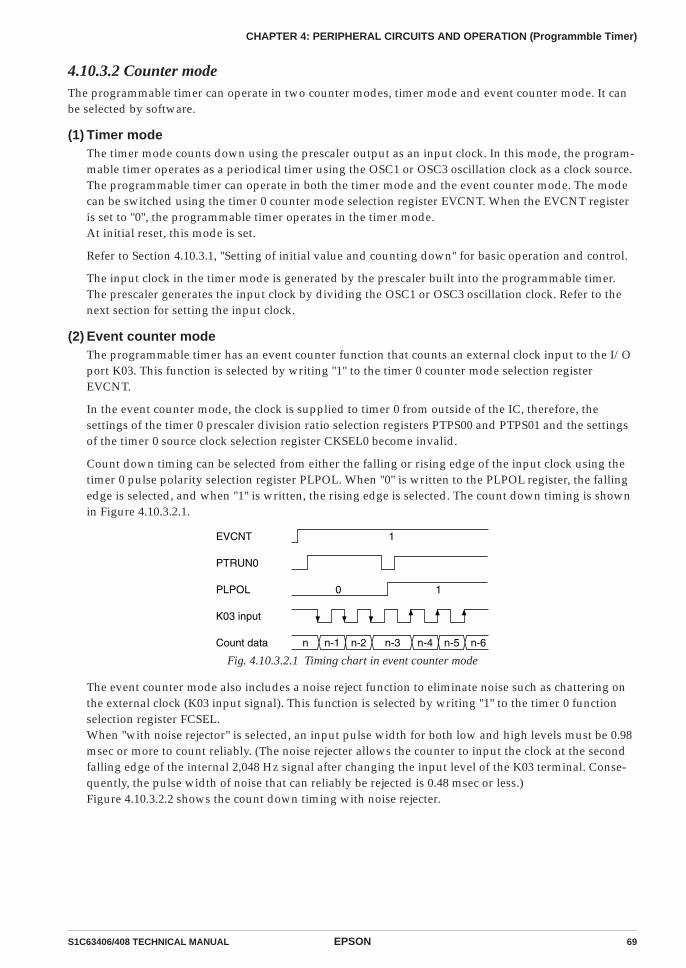
S1C63406/408 TECHNICAL MANUAL EPSON 69
CHAPTER 4: PERIPHERAL CIRCUITS AND OPERATION (Programmble Timer)
4.10.3.2 Counter modeThe programmable timer can operate in two counter modes, timer mode and event counter mode. It canbe selected by software.
(1) Timer modeThe timer mode counts down using the prescaler output as an input clock. In this mode, the program-mable timer operates as a periodical timer using the OSC1 or OSC3 oscillation clock as a clock source.The programmable timer can operate in both the timer mode and the event counter mode. The modecan be switched using the timer 0 counter mode selection register EVCNT. When the EVCNT registeris set to "0", the programmable timer operates in the timer mode.At initial reset, this mode is set.
Refer to Section 4.10.3.1, "Setting of initial value and counting down" for basic operation and control.
The input clock in the timer mode is generated by the prescaler built into the programmable timer.The prescaler generates the input clock by dividing the OSC1 or OSC3 oscillation clock. Refer to thenext section for setting the input clock.
(2) Event counter modeThe programmable timer has an event counter function that counts an external clock input to the I/Oport K03. This function is selected by writing "1" to the timer 0 counter mode selection registerEVCNT.
In the event counter mode, the clock is supplied to timer 0 from outside of the IC, therefore, thesettings of the timer 0 prescaler division ratio selection registers PTPS00 and PTPS01 and the settingsof the timer 0 source clock selection register CKSEL0 become invalid.
Count down timing can be selected from either the falling or rising edge of the input clock using thetimer 0 pulse polarity selection register PLPOL. When "0" is written to the PLPOL register, the fallingedge is selected, and when "1" is written, the rising edge is selected. The count down timing is shownin Figure 4.10.3.2.1.
K03 input
Count data n n-1 n-2 n-3 n-4 n-5 n-6
PLPOL
EVCNT
0 1
1
PTRUN0
Fig. 4.10.3.2.1 Timing chart in event counter mode
The event counter mode also includes a noise reject function to eliminate noise such as chattering onthe external clock (K03 input signal). This function is selected by writing "1" to the timer 0 functionselection register FCSEL.When "with noise rejector" is selected, an input pulse width for both low and high levels must be 0.98msec or more to count reliably. (The noise rejecter allows the counter to input the clock at the secondfalling edge of the internal 2,048 Hz signal after changing the input level of the K03 terminal. Conse-quently, the pulse width of noise that can reliably be rejected is 0.48 msec or less.)Figure 4.10.3.2.2 shows the count down timing with noise rejecter.
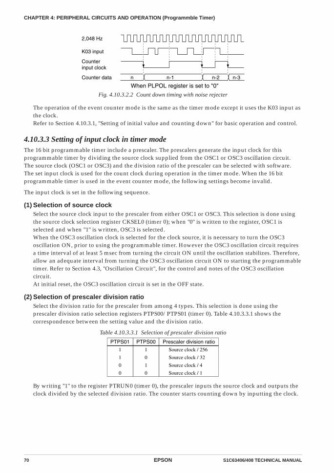
70 EPSON S1C63406/408 TECHNICAL MANUAL
CHAPTER 4: PERIPHERAL CIRCUITS AND OPERATION (Programmble Timer)
Counterinput clock
Counter data n n-1 n-2 n-3
K03 input
2,048 Hz
When PLPOL register is set to "0"
Fig. 4.10.3.2.2 Count down timing with noise rejecter
The operation of the event counter mode is the same as the timer mode except it uses the K03 input asthe clock.Refer to Section 4.10.3.1, "Setting of initial value and counting down" for basic operation and control.
4.10.3.3 Setting of input clock in timer modeThe 16 bit programmable timer include a prescaler. The prescalers generate the input clock for thisprogrammable timer by dividing the source clock supplied from the OSC1 or OSC3 oscillation circuit.The source clock (OSC1 or OSC3) and the division ratio of the prescaler can be selected with software.The set input clock is used for the count clock during operation in the timer mode. When the 16 bitprogrammable timer is used in the event counter mode, the following settings become invalid.
The input clock is set in the following sequence.
(1) Selection of source clockSelect the source clock input to the prescaler from either OSC1 or OSC3. This selection is done usingthe source clock selection register CKSEL0 (timer 0); when "0" is written to the register, OSC1 isselected and when "1" is written, OSC3 is selected.When the OSC3 oscillation clock is selected for the clock source, it is necessary to turn the OSC3oscillation ON, prior to using the programmable timer. However the OSC3 oscillation circuit requiresa time interval of at least 5 msec from turning the circuit ON until the oscillation stabilizes. Therefore,allow an adequate interval from turning the OSC3 oscillation circuit ON to starting the programmabletimer. Refer to Section 4.3, "Oscillation Circuit", for the control and notes of the OSC3 oscillationcircuit.At initial reset, the OSC3 oscillation circuit is set in the OFF state.
(2) Selection of prescaler division ratioSelect the division ratio for the prescaler from among 4 types. This selection is done using theprescaler division ratio selection registers PTPS00/PTPS01 (timer 0). Table 4.10.3.3.1 shows thecorrespondence between the setting value and the division ratio.
Table 4.10.3.3.1 Selection of prescaler division ratio
PTPS01
1
1
0
0
PTPS00
1
0
1
0
Prescaler division ratio
Source clock / 256
Source clock / 32
Source clock / 4
Source clock / 1
By writing "1" to the register PTRUN0 (timer 0), the prescaler inputs the source clock and outputs theclock divided by the selected division ratio. The counter starts counting down by inputting the clock.
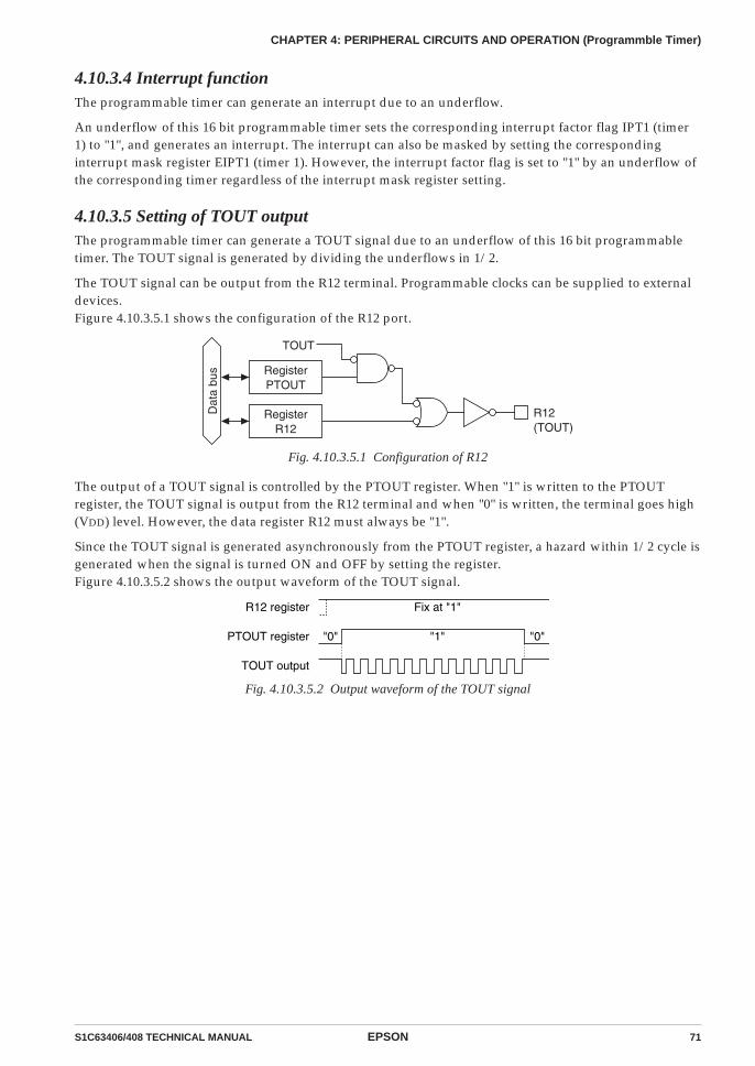
S1C63406/408 TECHNICAL MANUAL EPSON 71
CHAPTER 4: PERIPHERAL CIRCUITS AND OPERATION (Programmble Timer)
4.10.3.4 Interrupt functionThe programmable timer can generate an interrupt due to an underflow.
An underflow of this 16 bit programmable timer sets the corresponding interrupt factor flag IPT1 (timer1) to "1", and generates an interrupt. The interrupt can also be masked by setting the correspondinginterrupt mask register EIPT1 (timer 1). However, the interrupt factor flag is set to "1" by an underflow ofthe corresponding timer regardless of the interrupt mask register setting.
4.10.3.5 Setting of TOUT outputThe programmable timer can generate a TOUT signal due to an underflow of this 16 bit programmabletimer. The TOUT signal is generated by dividing the underflows in 1/2.
The TOUT signal can be output from the R12 terminal. Programmable clocks can be supplied to externaldevices.Figure 4.10.3.5.1 shows the configuration of the R12 port.
Dat
a bu
s RegisterPTOUT
RegisterR12
TOUT
R12(TOUT)
Fig. 4.10.3.5.1 Configuration of R12
The output of a TOUT signal is controlled by the PTOUT register. When "1" is written to the PTOUTregister, the TOUT signal is output from the R12 terminal and when "0" is written, the terminal goes high(VDD) level. However, the data register R12 must always be "1".
Since the TOUT signal is generated asynchronously from the PTOUT register, a hazard within 1/2 cycle isgenerated when the signal is turned ON and OFF by setting the register.Figure 4.10.3.5.2 shows the output waveform of the TOUT signal.
R12 register
PTOUT register
TOUT output
Fix at "1"
"1""0" "0"
Fig. 4.10.3.5.2 Output waveform of the TOUT signal

72 EPSON S1C63406/408 TECHNICAL MANUAL
CHAPTER 4: PERIPHERAL CIRCUITS AND OPERATION (Programmble Timer)
4.10.3.6 Transfer rate setting for serial interfaceThe signal that is made from underflows of the 16 bit programmable timer by dividing them in 1/2, canbe used as the clock source for the serial interface.The programmable timer outputs the clock to the serial interface by setting this 16 bit programmabletimer into RUN state (PTRUN0 = "1"). It is not necessary to control with the PTOUT register.
PTRUN0
16 bit programmable timer underfrow
Source clock for serial I/F
Fig. 4.10.3.6.1 Synchronous clock of serial interface
A setting value for the RLD1X register according to a transfer rate is calculated by the following expres-sion:
RLD1X, RLD0X = fosc / (2 ∗ bps ∗ division ratio of the prescaler) - 1fosc: Oscillation frequency (OSC1/OSC3)bps: Transfer rate(00H can be set to RLD1X)
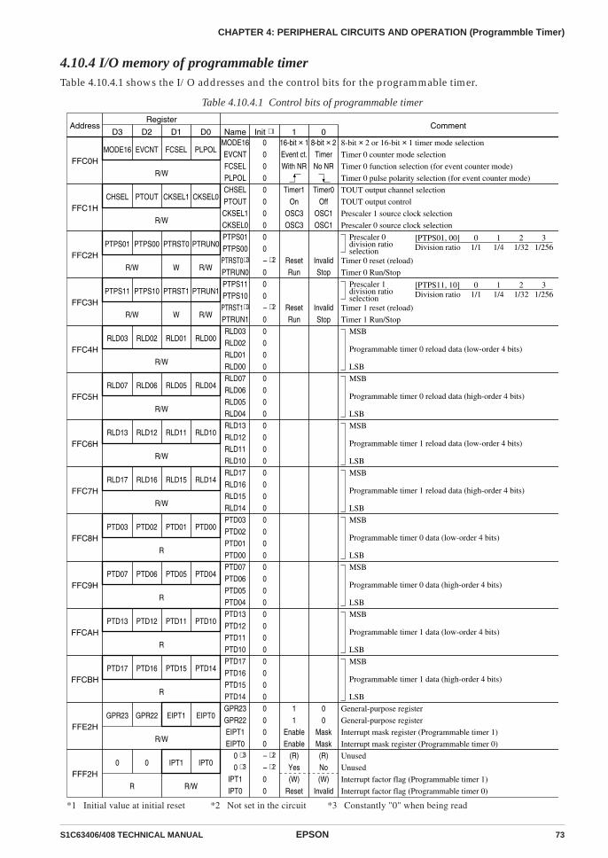
S1C63406/408 TECHNICAL MANUAL EPSON 73
CHAPTER 4: PERIPHERAL CIRCUITS AND OPERATION (Programmble Timer)
4.10.4 I/O memory of programmable timerTable 4.10.4.1 shows the I/O addresses and the control bits for the programmable timer.
Table 4.10.4.1 Control bits of programmable timer
Address CommentD3 D2
Register
D1 D0 Name Init ∗ 1 1 0
CHSELPTOUTCKSEL1CKSEL0
0000
Timer1On
OSC3OSC3
Timer0Off
OSC1OSC1
TOUT output channel selection
TOUT output control
Prescaler 1 source clock selection
Prescaler 0 source clock selectionR/W
FFC1HCHSEL PTOUT CKSEL1 CKSEL0
PTPS01PTPS00PTRST0∗ 3
PTRUN0
00
– ∗ 2
0ResetRun
InvalidStop
Prescaler 0 division ratio selectionTimer 0 reset (reload)
Timer 0 Run/StopW R/WR/W
FFC2HPTPS01 PTPS00 PTRST0 PTRUN0
01/1
11/4
21/32
31/256
[PTPS01, 00]Division ratio
PTPS11PTPS10PTRST1∗ 3
PTRUN1
00
– ∗ 2
0ResetRun
InvalidStop
Prescaler 1 division ratio selectionTimer 1 reset (reload)
Timer 1 Run/StopW R/WR/W
FFC3HPTPS11 PTPS10 PTRST1 PTRUN1
RLD03RLD02RLD01RLD00
0000
MSB
Programmable timer 0 reload data (low-order 4 bits)
LSBR/W
FFC4HRLD03 RLD02 RLD01 RLD00
RLD07RLD06RLD05RLD04
0000
MSB
Programmable timer 0 reload data (high-order 4 bits)
LSBR/W
FFC5HRLD07 RLD06 RLD05 RLD04
RLD13RLD12RLD11RLD10
0000
MSB
Programmable timer 1 reload data (low-order 4 bits)
LSBR/W
FFC6HRLD13 RLD12 RLD11 RLD10
RLD17RLD16RLD15RLD14
0000
MSB
Programmable timer 1 reload data (high-order 4 bits)
LSBR/W
FFC7HRLD17 RLD16 RLD15 RLD14
PTD03PTD02PTD01PTD00
0000
MSB
Programmable timer 0 data (low-order 4 bits)
LSBR
FFC8HPTD03 PTD02 PTD01 PTD00
PTD07PTD06PTD05PTD04
0000
MSB
Programmable timer 0 data (high-order 4 bits)
LSBR
FFC9HPTD07 PTD06 PTD05 PTD04
PTD13PTD12PTD11PTD10
0000
MSB
Programmable timer 1 data (low-order 4 bits)
LSBR
FFCAHPTD13 PTD12 PTD11 PTD10
PTD17PTD16PTD15PTD14
0000
MSB
Programmable timer 1 data (high-order 4 bits)
LSBR
FFCBHPTD17 PTD16 PTD15 PTD14
01/1
11/4
21/32
31/256
[PTPS11, 10]Division ratio
FFF2H0 0 IPT1 IPT0
R R/W
0 ∗ 3
0 ∗ 3
IPT1IPT0
– ∗ 2
– ∗ 2
00
(R)Yes(W)
Reset
(R)No(W)
Invalid
Unused
Unused
Interrupt factor flag (Programmable timer 1)
Interrupt factor flag (Programmable timer 0)
FFE2HGPR23 GPR22 EIPT1 EIPT0
R/W
GPR23GPR22EIPT1EIPT0
0000
11
EnableEnable
00
MaskMask
General-purpose register
General-purpose register
Interrupt mask register (Programmable timer 1)
Interrupt mask register (Programmable timer 0)
MODE16EVCNTFCSELPLPOL
0000
16-bit × 1Event ct.With NR
8-bit × 2TimerNo NR
8-bit × 2 or 16-bit × 1 timer mode selection
Timer 0 counter mode selection
Timer 0 function selection (for event counter mode)
Timer 0 pulse polarity selection (for event counter mode)R/W
FFC0HMODE16 EVCNT FCSEL PLPOL
*1 Initial value at initial reset *2 Not set in the circuit *3 Constantly "0" when being read
74 EPSON S1C63406/408 TECHNICAL MANUAL
CHAPTER 4: PERIPHERAL CIRCUITS AND OPERATION (Programmble Timer)
CKSEL0: Prescaler 0 source clock selection register (FFC1H•D0)CKSEL1: Prescaler 1 source clock selection register (FFC1H•D1)Selects the source clock of the prescaler.
When "1" is written: OSC3 clockWhen "0" is written: OSC1 clock
Reading: Valid
The source clock for the prescaler is selected from OSC1 or OSC3. When "0" is written to the CKSEL0register, the OSC1 clock is selected as the input clock for the prescaler 0 (for timer 0) and when "1" iswritten, the OSC3 clock is selected.Same as above, the source clock for prescaler 1 is selected by the CKSEL1 register.When the event counter mode is selected to timer 0, the setting of the CKSEL0 register becomes invalid.At initial reset, these registers are set to "0".
PTPS00, PTPS01: Timer 0 prescaler division ratio selection register (FFC2H•D2, D3)PTPS10, PTPS11: Timer 1 prescaler division ratio selection register (FFC3H•D2, D3)Selects the division ratio of the prescaler.Two bits of PTPS00 and PTPS01 are the prescaler division ratio selection register for timer 0, and two bitsof PTPS10 and PTPS11 are for timer 1. The prescaler division ratios that can be set by these registers areshown in Table 4.10.4.2.
Table 4.10.4.2 Selection of prescaler division ratio
PTPS11
PTPS01
1
1
0
0
PTPS10
PTPS00
1
0
1
0
Prescaler division ratio
Source clock / 256
Source clock / 32
Source clock / 4
Source clock / 1
When the event counter mode is selected to timer 0, the setting of the PTPS00 and PTPS01 becomesinvalid.At initial reset, these registers are set to "0".
EVCNT: Timer 0 counter mode selection register (FFC0H•D2)Selects a counter mode for timer 0.
When "1" is written: Event counter modeWhen "0" is written: Timer mode
Reading: Valid
The counter mode for timer 0 is selected from either the event counter mode or timer mode. When "1" iswritten to the EVCNT register, the event counter mode is selected and when "0" is written, the timermode is selected.At initial reset, this register is set to "0".
MODE16: 8-bit × 2 or 16-bit × 1 timer mode selection register (FFC0H•D3)Selects 8-bit × 2 channels mode (timer 0 and timer 1) or 16-bit × 1 channel mode.
When "1" is written: 16-bit × 1 channelWhen "0" is written: 8-bit × 2 channels (timer 0 and timer 1)
Reading: Valid
When 8-bit × 2 channels is selected, timer 0 and timer 1 can be used independently.When 16-bit × 1 channel is selected, timer 0 and timer 1 are chained together and are used as a 16-bitprogrammable timer. The clock is input to timer 0 and interrupts will be generated from timer 1.At initial reset, this register is set to "0".

S1C63406/408 TECHNICAL MANUAL EPSON 75
CHAPTER 4: PERIPHERAL CIRCUITS AND OPERATION (Programmble Timer)
FCSEL: Timer 0 function selection register (FFC0H•D1)Selects whether the noise rejector of the clock input circuit will be used or not in the event counter mode.
When "1" is written: With noise rejecterWhen "0" is written: Without noise rejecter
Reading: Valid
When "1" is written to the FCSEL register, the noise rejecter is used and counting is done by an externalclock (K03) with 0.98 msec or more pulse width. (The noise rejecter allows the counter to input the clockat the second falling edge of the internal 2,048 Hz signal after changing the input level of the K03 termi-nal. Consequently, the pulse width of noise that can reliably be rejected is 0.48 msec or less.)When "0" is written to the FCSEL register, the noise rejector is not used and the counting is done directlyby an external clock input to the K03 terminal.Setting of this register is effective only when timer 0 is used in the event counter mode.At initial reset, this register is set to "0".
PLPOL: Timer 0 pulse polarity selection register (FFC0H•D0)Selects the count pulse polarity in the event counter mode.
When "1" is written: Rising edgeWhen "0" is written: Falling edge
Reading: Valid
The count timing in the event counter mode (timer 0) is selected from either the falling edge of theexternal clock input to the K03 terminal or the rising edge. When "0" is written to the PLPOL register, thefalling edge is selected and when "1" is written, the rising edge is selected.Setting of this register is effective only when timer 0 is used in the event counter mode.At initial reset, this register is set to "0".
RLD00–RLD07: Timer 0 reload data register (FFC4H, FFC5H)RLD10–RLD17: Timer 1 reload data register (FFC6H, FFC7H)Sets the initial value for the counter.The reload data written in this register is loaded to the respective counters. The counter counts downusing the data as the initial value for counting.Reload data is loaded to the counter when the counter is reset by writing "1" to the PTRST0 or PTRST1register, or when counter underflow occurs.At initial reset, these registers are set to "00H".
PTD00–PTD07: Timer 0 counter data (FFC8H, FFC9H)PTD10–PTD17: Timer 1 counter data (FFCAH, FFCBH)Count data in the programmable timer can be read from these latches.The low-order 4 bits of the count data in timer 0 can be read from PTD00–PTD03, and the high-order datacan be read from PTD04–PTD07. Similarly, for timer 1, the low-order 4 bits can be read from PTD10–PTD13, and the high-order data can be read from PTD14–PTD17.Since the high-order 4 bits are held by reading the low-order 4 bits, be sure to read the low-order 4 bitsfirst.Since these latches are exclusively for reading, the writing operation is invalid.At initial reset, these counter data are set to "00H".

76 EPSON S1C63406/408 TECHNICAL MANUAL
CHAPTER 4: PERIPHERAL CIRCUITS AND OPERATION (Programmble Timer)
PTRST0: Timer 0 reset (reload) (FFC2H•D1)PTRST1: Timer 1 reset (reload) (FFC3H•D1)Resets the timer and presets reload data to the counter.
When "1" is written: ResetWhen "0" is written: No operation
Reading: Always "0"
By writing "1" to PTRST0, the reload data in the reload register RLD00–RLD07 is preset to the counter intimer 0. Similarly, the reload data in RLD10–RLD17 is preset to the counter in timer 1 by PTRST1.When the counter is preset in the RUN status, the counter restarts immediately after presetting. In thecase of STOP status, the reload data is preset to the counter and is maintained.No operation results when "0" is written.Since these bits are exclusively for writing, always set to "0" during reading.
PTRUN0: Timer 0 RUN/STOP control register (FFC2H•D0)PTRUN1: Timer 1 RUN/STOP control register (FFC3H•D0)Controls the RUN/STOP of the counter.
When "1" is written: RUNWhen "0" is written: STOP
Reading: Valid
The counter in timer 0 starts counting down by writing "1" to the PTRUN0 register and stops by writing"0".In STOP status, the counter data is maintained until the counter is reset or is set in the next RUN status.When STOP status changes to RUN status, the data that has been maintained can be used for resumingthe count.Same as above, the timer 1 counter is controlled by the PTRUN1 register.At initial reset, these registers are set to "0".
CHSEL: TOUT output channel selection register (FFC1H•D3)Selects the channel used for TOUT signal output.
When "1" is written: Timer 1When "0" is written: Timer 0
Reading: Valid
This register selects which timer's underflow (timer 0 or timer 1) is used to generate a TOUT signal. When"0" is written to the CHSEL register, timer 0 is selected and when "1" is written, timer 1 is selected. In the16-bit × 2 channels mode (MODE16 = "1"), timer 1 is always selected regardless of this register setting.At initial reset, this register is set to "0".
PTOUT: TOUT output control register (FFC1H•D2)Turns TOUT signal output ON and OFF.
When "1" is written: ONWhen "0" is written: OFF
Reading: Valid
PTOUT is the output control register for the TOUT signal. When "1" is written to the register, the TOUTsignal is output from the R12 terminal and when "0" is written, the terminal goes high (VDD) level.However, the data register R12 must always be "1".At initial reset, this register is set to "0".
S1C63406/408 TECHNICAL MANUAL EPSON 77
CHAPTER 4: PERIPHERAL CIRCUITS AND OPERATION (Programmble Timer)
EIPT0: Timer 0 interrupt mask register (FFE2H•D0)EIPT1: Timer 1 interrupt mask register (FFE2H•D1)These registers are used to select whether to mask the programmable timer interrupt or not.
When "1" is written: EnabledWhen "0" is written: Masked
Reading: Valid
Timer 0 and timer 1 interrupts can be masked individually by the interrupt mask registers EIPT0 (timer 0)and EIPT1 (timer 1).At initial reset, these registers are set to "0".
IPT0: Timer 0 interrupt factor flag (FFF2H•D0)IPT1: Timer 1 interrupt factor flag (FFF2H•D1)These flags indicate the status of the programmable timer interrupt.
When "1" is read: Interrupt has occurredWhen "0" is read: Interrupt has not occurred
When "1" is written: Flag is resetWhen "0" is written: Invalid
The interrupt factor flags IPT0 and IPT1 correspond to timer 0 and timer 1 interrupts, respectively. Thesoftware can judge from these flags whether there is a programmable timer interrupt. However, even ifthe interrupt is masked, the flags are set to "1" by the underflows of the corresponding counters.These flags are reset to "0" by writing "1" to them.After an interrupt occurs, the same interrupt will occur again if the interrupt enabled state (I flag = "1") isset or the RETI instruction is executed unless the interrupt factor flag is reset. Therefore, be sure to reset(write "1" to) the interrupt factor flag in the interrupt service routine before shifting to the interruptenabled state.At initial reset, these flags are set to "0".

78 EPSON S1C63406/408 TECHNICAL MANUAL
CHAPTER 4: PERIPHERAL CIRCUITS AND OPERATION (Programmble Timer)
4.10.5 Programming notes(1) When reading counter data, be sure to read the low-order 4 bits (PTD00–PTD03, PTD10–PTD13) first.
Furthermore, the high-order 4 bits (PTD04–PTD07, PTD14–PTD17) should be read within 0.73 msec ofreading the low-order 4 bits (PTD00–PTD03, PTD10–PTD13).For the 16 bit × 1 mode, be sure to read as following sequence:
(PTD00–PTD03) → (PTD04–PTD07) → (PTD10–PTD13) → (PTD14–PTD17)The read sequence time should be within 1.46 msec.
(2) The programmable timer actually enters RUN/STOP status in synchronization with the falling edgeof the input clock after writing to the PTRUN0/PTRUN1 register. Consequently, when "0" is written tothe PTRUN0/PTRUN1 register, the timer enters STOP status at the point where the counter isdecremented (-1). The PTRUN0/PTRUN1 register maintains "1" for reading until the timer actuallystops.Figure 4.10.5.1 shows the timing chart for the RUN/STOP control.
PTRUN0/PTRUN1 (WR)
PTD0X/PTD1X 42H 41H 40H 3FH 3EH 3DH
PTRUN0/PTRUN1 (RD)
Input clock
"1" (RUN) writing
"0" (STOP) writing
Fig. 4.10.5.1 Timing chart for RUN/STOP control
It is the same even in the event counter mode. Therefore, be aware that the counter does not enterRUN/STOP status if a clock is not input after setting the RUN/STOP control register (PTRUN0).
(3) Since the TOUT signal is generated asynchronously from the PTOUT register, a hazard within 1/2cycle is generated when the signal is turned ON and OFF by setting the register.
(4) When the OSC3 oscillation clock is selected for the clock source, it is necessary to turn the OSC3oscillation ON, prior to using the programmable timer. However the OSC3 oscillation circuit requiresa time interval of at least 5 msec from turning the circuit ON until the oscillation stabilizes. Therefore,allow an adequate interval from turning the OSC3 oscillation circuit ON to starting the programmabletimer. Refer to Section 4.3, "Oscillation Circuit", for the control and notes of the OSC3 oscillationcircuit.At initial reset, the OSC3 oscillation circuit is set in the OFF state.
(5) After an interrupt occurs, the same interrupt will occur again if the interrupt enabled state (I flag ="1") is set or the RETI instruction is executed unless the interrupt factor flag is reset. Therefore, be sureto reset (write "1" to) the interrupt factor flag in the interrupt service routine before shifting to theinterrupt enabled state.
(6) For the reason below, pay attention to the reload data write timing when changing the interval of theprogrammable timer interrupts while the programmable timer is running.The programmable timer counts down at the falling edge of the input clock and at the same time itgenerates an interrupt if the counter underflows. Then it starts loading the reload data to the counterand the counter data is determined at the next rising edge of the input clock (period shown in as ➀ inthe figure).
Input clock
Counter data (continuous mode) (Reload data = 25H)03H 02H 01H 00H 25H 24H
Counter data is determined by reloading.Underflow (interrupt is generated)
➀
Fig. 4.10.5.2 Reload timing for programmable timer
To avoid improper reloading, do not rewrite the reload data after an interrupt occurs until the counterdata is determined including the reloading period ➀ . Be especially careful when using the OSC1 (low-speed clock) as the clock source of the programmable timer and the CPU is operating with OSC3(high-speed clock).
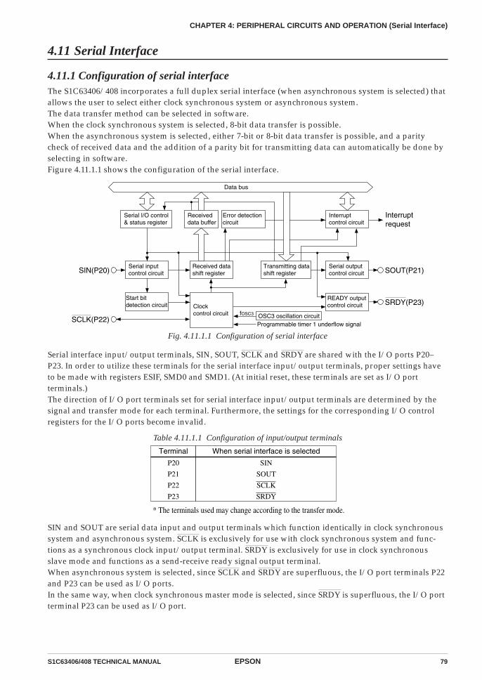
S1C63406/408 TECHNICAL MANUAL EPSON 79
CHAPTER 4: PERIPHERAL CIRCUITS AND OPERATION (Serial Interface)
4.11 Serial Interface
4.11.1 Configuration of serial interfaceThe S1C63406/408 incorporates a full duplex serial interface (when asynchronous system is selected) thatallows the user to select either clock synchronous system or asynchronous system.The data transfer method can be selected in software.When the clock synchronous system is selected, 8-bit data transfer is possible.When the asynchronous system is selected, either 7-bit or 8-bit data transfer is possible, and a paritycheck of received data and the addition of a parity bit for transmitting data can automatically be done byselecting in software.Figure 4.11.1.1 shows the configuration of the serial interface.
fOSC3
Data bus
SOUT(P21)
Serial I/O control& status register
Receiveddata buffer
Interruptcontrol circuit
Serial inputcontrol circuit
Received datashift register
Transmitting datashift register
Serial outputcontrol circuitSIN(P20)
Clockcontrol circuit
READY outputcontrol circuit
SCLK(P22)
Error detectioncircuit
SRDY(P23)Start bitdetection circuit
Programmable timer 1 underflow signal
Interruptrequest
OSC3 oscillation circuit
Fig. 4.11.1.1 Configuration of serial interface
Serial interface input/output terminals, SIN, SOUT, SCLK and SRDY are shared with the I/O ports P20–P23. In order to utilize these terminals for the serial interface input/output terminals, proper settings haveto be made with registers ESIF, SMD0 and SMD1. (At initial reset, these terminals are set as I/O portterminals.)The direction of I/O port terminals set for serial interface input/output terminals are determined by thesignal and transfer mode for each terminal. Furthermore, the settings for the corresponding I/O controlregisters for the I/O ports become invalid.
Table 4.11.1.1 Configuration of input/output terminals
Terminal When serial interface is selected
P20
P21
P22
P23
SIN
SOUT
SCLK
SRDY
* The terminals used may change according to the transfer mode.
SIN and SOUT are serial data input and output terminals which function identically in clock synchronoussystem and asynchronous system. SCLK is exclusively for use with clock synchronous system and func-tions as a synchronous clock input/output terminal. SRDY is exclusively for use in clock synchronousslave mode and functions as a send-receive ready signal output terminal.When asynchronous system is selected, since SCLK and SRDY are superfluous, the I/O port terminals P22and P23 can be used as I/O ports.In the same way, when clock synchronous master mode is selected, since SRDY is superfluous, the I/O portterminal P23 can be used as I/O port.
80 EPSON S1C63406/408 TECHNICAL MANUAL
CHAPTER 4: PERIPHERAL CIRCUITS AND OPERATION (Serial Interface)
4.11.2 Mask optionSince the input/output terminals of the serial interface is shared with the I/O ports (P20–P23), the maskoption that selects the output specification for the I/O port is also applied to the serial interface.The output specification of the terminals SOUT, SCLK (for clock synchronous master mode) and SRDY(for clock synchronous slave mode) that are used as output in the input/output port of the serial interfaceis respectively selected by the mask options of P21, P22 and P23. Either complementary output or N-channel open drain output can be selected as the output specification. However, when N-channel opendrain output is selected, do not apply a voltage exceeding the power supply voltage to the terminal.
4.11.3 Transfer modesThere are four transfer modes for the serial interface and mode selection is made by setting the two bits ofthe mode selection registers SMD0 and SMD1 as shown in the table below.
Table 4.11.3.1 Transfer modes
SMD1 SMD0 Mode
1
1
0
0
1
0
1
0
8-bit asynchronous
7-bit asynchronous
Clock synchronous slave
Clock synchronous master
Table 4.11.3.2 Terminal settings corresponding to each transfer mode
Mode SIN
Asynchronous 8-bit
Asynchronous 7-bit
Clock synchronous slave
Clock synchronous master
P23
P23
Output
P23
SOUT SCLK SRDY
P22
P22
Input
Output
Output
Output
Output
Output
Input
Input
Input
Input
At initial reset, transfer mode is set to clock synchronous master mode.
Clock synchronous master modeIn this mode, the internal clock is utilized as a synchronous clock for the built-in shift registers, and 8-bit clock synchronous serial transfers can be performed with this serial interface as the master.The synchronous clock is also output from the SCLK terminal which enables control of the external(slave side) serial I/O device. Since the SRDY terminal is not utilized in this mode, it can be used as anI/O port.Figure 4.11.3.1(a) shows the connection example of input/output terminals in the clock synchronousmaster mode.
Clock synchronous slave modeIn this mode, a synchronous clock from the external (master side) serial input/output device isutilized and 8-bit clock synchronous serial transfers can be performed with this serial interface as theslave.The synchronous clock is input to the SCLK terminal and is utilized by this interface as the synchro-nous clock.Furthermore, the SRDY signal indicating the transmit-receive ready status is output from the SRDYterminal in accordance with the serial interface operating status.In the slave mode, the settings for registers SCS0 and SCS1 used to select the clock source are invalid.Figure 4.11.3.1(b) shows the connection example of input/output terminals in the clock synchronousslave mode.
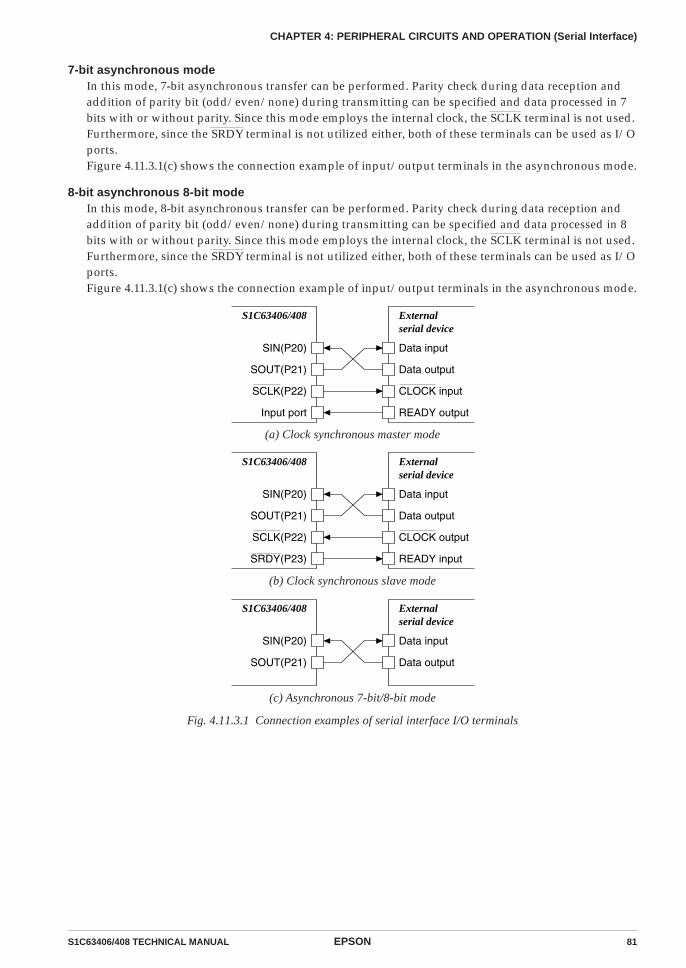
S1C63406/408 TECHNICAL MANUAL EPSON 81
CHAPTER 4: PERIPHERAL CIRCUITS AND OPERATION (Serial Interface)
7-bit asynchronous modeIn this mode, 7-bit asynchronous transfer can be performed. Parity check during data reception andaddition of parity bit (odd/even/none) during transmitting can be specified and data processed in 7bits with or without parity. Since this mode employs the internal clock, the SCLK terminal is not used.Furthermore, since the SRDY terminal is not utilized either, both of these terminals can be used as I/Oports.Figure 4.11.3.1(c) shows the connection example of input/output terminals in the asynchronous mode.
8-bit asynchronous 8-bit modeIn this mode, 8-bit asynchronous transfer can be performed. Parity check during data reception andaddition of parity bit (odd/even/none) during transmitting can be specified and data processed in 8bits with or without parity. Since this mode employs the internal clock, the SCLK terminal is not used.Furthermore, since the SRDY terminal is not utilized either, both of these terminals can be used as I/Oports.Figure 4.11.3.1(c) shows the connection example of input/output terminals in the asynchronous mode.
Data input
Data output
CLOCK input
READY output
SIN(P20)
SOUT(P21)
SCLK(P22)
Input port
Externalserial device
S1C63406/408
(a) Clock synchronous master mode
Data input
Data output
CLOCK output
READY input
SIN(P20)
SOUT(P21)
SCLK(P22)
SRDY(P23)
Externalserial device
S1C63406/408
(b) Clock synchronous slave mode
Data input
Data output
SIN(P20)
SOUT(P21)
Externalserial device
S1C63406/408
(c) Asynchronous 7-bit/8-bit mode
Fig. 4.11.3.1 Connection examples of serial interface I/O terminals
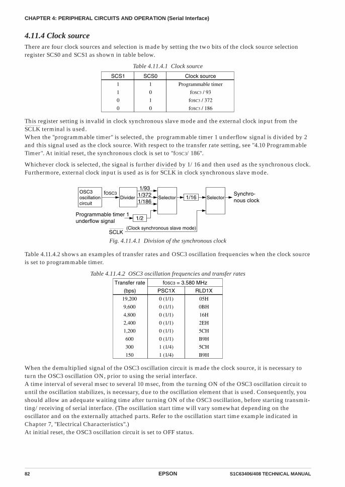
82 EPSON S1C63406/408 TECHNICAL MANUAL
CHAPTER 4: PERIPHERAL CIRCUITS AND OPERATION (Serial Interface)
4.11.4 Clock sourceThere are four clock sources and selection is made by setting the two bits of the clock source selectionregister SCS0 and SCS1 as shown in table below.
Table 4.11.4.1 Clock source
SCS1
1
1
0
0
SCS0
1
0
1
0
Clock source
Programmable timer
fOSC3 / 93
fOSC3 / 372
fOSC3 / 186
This register setting is invalid in clock synchronous slave mode and the external clock input from theSCLK terminal is used.When the "programmable timer" is selected, the programmable timer 1 underflow signal is divided by 2and this signal used as the clock source. With respect to the transfer rate setting, see "4.10 ProgrammableTimer". At initial reset, the synchronous clock is set to "fOSC3/186".
Whichever clock is selected, the signal is further divided by 1/16 and then used as the synchronous clock.Furthermore, external clock input is used as is for SCLK in clock synchronous slave mode.
fOSC31/93
1/3721/186
1/16Synchro-nous clock
Programmable timer 1underflow signal
SCLK(Clock synchronous slave mode)
Divider Selector Selector
1/2
OSC3oscillationcircuit
Fig. 4.11.4.1 Division of the synchronous clock
Table 4.11.4.2 shows an examples of transfer rates and OSC3 oscillation frequencies when the clock sourceis set to programmable timer.
Table 4.11.4.2 OSC3 oscillation frequencies and transfer rates
Transfer rate
(bps)
19,200
9,600
4,800
2,400
1,200
600
300
150
fOSC3 = 3.580 MHz
PSC1X
0 (1/1)
0 (1/1)
0 (1/1)
0 (1/1)
0 (1/1)
0 (1/1)
1 (1/4)
1 (1/4)
RLD1X
05H
0BH
16H
2EH
5CH
B9H
5CH
B9H
When the demultiplied signal of the OSC3 oscillation circuit is made the clock source, it is necessary toturn the OSC3 oscillation ON, prior to using the serial interface.A time interval of several msec to several 10 msec, from the turning ON of the OSC3 oscillation circuit tountil the oscillation stabilizes, is necessary, due to the oscillation element that is used. Consequently, youshould allow an adequate waiting time after turning ON of the OSC3 oscillation, before starting transmit-ting/receiving of serial interface. (The oscillation start time will vary somewhat depending on theoscillator and on the externally attached parts. Refer to the oscillation start time example indicated inChapter 7, "Electrical Characteristics".)At initial reset, the OSC3 oscillation circuit is set to OFF status.
S1C63406/408 TECHNICAL MANUAL EPSON 83
CHAPTER 4: PERIPHERAL CIRCUITS AND OPERATION (Serial Interface)
4.11.5 Transmit-receive controlBelow is a description of the registers which handle transmit-receive control. With respect to transmit-receive control procedures and operations, please refer to the following sections in which these arediscussed on a mode by mode basis.
Shift register and receive data bufferExclusive shift registers for transmitting and receiving are installed in this serial interface. Conse-quently, duplex communication simultaneous transmit and receive is possible when the asynchronoussystem is selected.
Data being transmitted are written to TRXD0–TRXD7 and converted to serial through the shiftregister and is output from the SOUT terminal.
In the reception section, a receive data buffer is installed separate from the shift register.Data being received are input to the SIN terminal and is converted to parallel through the shiftregister and written to the receive data buffer.Since the receive data buffer can be read even during serial input operation, the continuous data isreceived efficiently.However, since buffer functions are not used in clock synchronous mode, be sure to read out databefore the next data reception begins.
Transmit enable register and transmit control bitFor transmit control, use the transmit enable register TXEN and transmit control bit TXTRG.
The transmit enable register TXEN is used to set the transmit enable/disable status. When "1" iswritten to this register to set the transmitting enable status, clock input to the shift register is enabledand the system is ready to transmit data. In the clock synchronous mode, synchronous clock input/output from the SCLK terminal is also enabled.
The transmit control bit TXTRG is used as the trigger to start transmitting data.Data to be transmitted is written to the transmit data shift register, and when transmitting prepara-tions a recomplete, "1" is written to TXTRG whereupon data transmitting begins.When interrupt has been enabled, an interrupt is generated when the transmission is completed. Ifthere is subsequent data to be transmitted it can be sent using this interrupt.In addition, TXTRG can be read as a status bit. When set to "1", it indicates transmitting operation,and "0" indicates transmitting stop.For details on timing, see the timing chart which gives the timing for each mode.
When not transmitting, set TXEN to "0" to disable transmition.
Receive enable register, receive control bitFor receiving control, use the receive enable register RXEN and receive control bit RXTRG.Receive enable register RXEN is used to set receiving enable/disable status. When "1" is written intothis register to set the receiving enable status, clock input to the shift register is enabled and thesystem is ready to receive data. In the clock synchronous mode, synchronous clock input/output fromthe SCLK terminal is also enabled.With the above setting, receiving begins and serial data input from the SIN terminal goes to the shiftregister.The operation of the receive control bit RXTRG is slightly different depending on whether a clocksynchronous system or an asynchronous system is being used.In the clock synchronous system, the receive control bit TXTRG is used as the trigger to start receivingdata.When received data has been read and the preparation for next data receiving is completed, write "1"into RXTRG to start receiving. (When "1" is written to RXTRG in slave mode, SRDY switches to "0".)
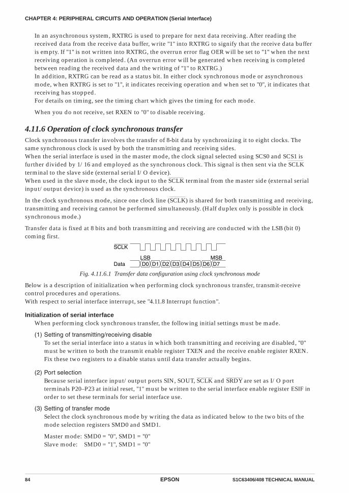
84 EPSON S1C63406/408 TECHNICAL MANUAL
CHAPTER 4: PERIPHERAL CIRCUITS AND OPERATION (Serial Interface)
In an asynchronous system, RXTRG is used to prepare for next data receiving. After reading thereceived data from the receive data buffer, write "1" into RXTRG to signify that the receive data bufferis empty. If "1" is not written into RXTRG, the overrun error flag OER will be set to "1" when the nextreceiving operation is completed. (An overrun error will be generated when receiving is completedbetween reading the received data and the writing of "1" to RXTRG.)In addition, RXTRG can be read as a status bit. In either clock synchronous mode or asynchronousmode, when RXTRG is set to "1", it indicates receiving operation and when set to "0", it indicates thatreceiving has stopped.For details on timing, see the timing chart which gives the timing for each mode.
When you do not receive, set RXEN to "0" to disable receiving.
4.11.6 Operation of clock synchronous transferClock synchronous transfer involves the transfer of 8-bit data by synchronizing it to eight clocks. Thesame synchronous clock is used by both the transmitting and receiving sides.When the serial interface is used in the master mode, the clock signal selected using SCS0 and SCS1 isfurther divided by 1/16 and employed as the synchronous clock. This signal is then sent via the SCLKterminal to the slave side (external serial I/O device).When used in the slave mode, the clock input to the SCLK terminal from the master side (external serialinput/output device) is used as the synchronous clock.
In the clock synchronous mode, since one clock line (SCLK) is shared for both transmitting and receiving,transmitting and receiving cannot be performed simultaneously. (Half duplex only is possible in clocksynchronous mode.)
Transfer data is fixed at 8 bits and both transmitting and receiving are conducted with the LSB (bit 0)coming first.
SCLK
Data D0 D1 D2 D3 D4 D5 D6 D7LSB MSB
Fig. 4.11.6.1 Transfer data configuration using clock synchronous mode
Below is a description of initialization when performing clock synchronous transfer, transmit-receivecontrol procedures and operations.With respect to serial interface interrupt, see "4.11.8 Interrupt function".
Initialization of serial interfaceWhen performing clock synchronous transfer, the following initial settings must be made.
(1) Setting of transmitting/receiving disableTo set the serial interface into a status in which both transmitting and receiving are disabled, "0"must be written to both the transmit enable register TXEN and the receive enable register RXEN.Fix these two registers to a disable status until data transfer actually begins.
(2) Port selectionBecause serial interface input/output ports SIN, SOUT, SCLK and SRDY are set as I/O portterminals P20–P23 at initial reset, "1" must be written to the serial interface enable register ESIF inorder to set these terminals for serial interface use.
(3) Setting of transfer modeSelect the clock synchronous mode by writing the data as indicated below to the two bits of themode selection registers SMD0 and SMD1.
Master mode: SMD0 = "0", SMD1 = "0"Slave mode: SMD0 = "1", SMD1 = "0"

S1C63406/408 TECHNICAL MANUAL EPSON 85
CHAPTER 4: PERIPHERAL CIRCUITS AND OPERATION (Serial Interface)
(4) Clock source selectionIn the master mode, select the synchronous clock source by writing data to the two bits of theclock source selection registers SCS0 and SCS1. (See Table 4.11.4.1.)This selection is not necessary in the slave mode.
The parity enable register EPR is also assigned to this address, however, since parity is not neces-sary in the clock synchronous mode, parity check will not take place regardless of how they areset.
(5) Clock source controlWhen the master mode is selected and programmable timer for the clock source is selected, settransfer rate on the programmable timer side. (See "4.10 Programmable Timer".)When the divided signal of OSC3 oscillation circuit is selected for the clock source, be sure that theOSC3 oscillation circuit is turned ON prior to commencing data transfer. (See "4.3 OscillationCircuit".)Note that the frequency of the serial interface clock is limited to a maximum of 2 MHz.
Data transmit procedureThe control procedure and operation during transmitting is as follows.
(1) Write "0" in the transmit enable register TXEN and the receive enable register RXEN to reset theserial interface.
(2) Write "1" in the transmit enable register TXEN to set into the transmitting enable status.
(3) Write the transmitting data into TRXD0–TRXD7.
(4) In case of the master mode, confirm the receiveready status on the slave side (external serial input/output device), if necessary. Wait until it reaches thereceive ready status.
(5) Write "1" in the transmit control bit TXTRG andstart transmitting.
In the master mode, this control causes the synchro-nous clock to change to enable and to be providedto the shift register for transmitting and outputfrom the SCLK terminal.In the slave mode, it waits for the synchronousclock to be input from the SCLK terminal.The transmitting data of the shift register shifts onebit at a time at each falling edge of the synchronousclock and is output from the SOUT terminal. Whenthe final bit (MSB) is output, the SOUT terminal ismaintained at that level, until the next transmittingbegins.
The transmitting complete interrupt factor flag ISTRis set to "1" at the point where the data transmittingof the shift register is completed. When interrupthas been enabled, a transmitting complete interruptis generated at this point.Set the following transmitting data using thisinterrupt.
(6) Repeat steps (3) to (5) for the number of bytes oftransmitting data, and then set the transmit disablestatus by writing "0" to the transmit enable registerTXEN, when the transmitting is completed.
Data transmitting
End
TXEN ← 0, RXEN ← 0
No
Yes
Transmit complete ?
Set transmitting data
to TRXD0–TRXD7
No
Yes
ISTR = 1 ?
TXEN ← 0
TXTRG ← 1
TXEN ← 1
No
Yes
Receiver ready ?In case of master mode
Fig. 4.11.6.2 Transmit procedure in clocksynchronous mode
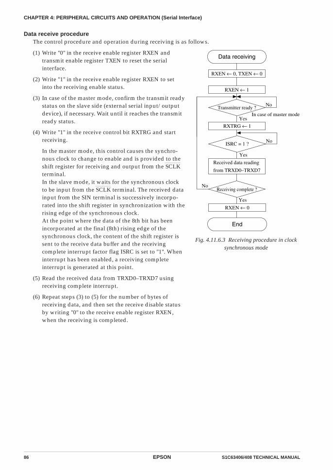
86 EPSON S1C63406/408 TECHNICAL MANUAL
CHAPTER 4: PERIPHERAL CIRCUITS AND OPERATION (Serial Interface)
(1) Write "0" in the receive enable register RXEN andtransmit enable register TXEN to reset the serialinterface.
(2) Write "1" in the receive enable register RXEN to setinto the receiving enable status.
(3) In case of the master mode, confirm the transmit readystatus on the slave side (external serial input/outputdevice), if necessary. Wait until it reaches the transmitready status.
(4) Write "1" in the receive control bit RXTRG and startreceiving.
In the master mode, this control causes the synchro-nous clock to change to enable and is provided to theshift register for receiving and output from the SCLKterminal.In the slave mode, it waits for the synchronous clockto be input from the SCLK terminal. The received datainput from the SIN terminal is successively incorpo-rated into the shift register in synchronization with therising edge of the synchronous clock.At the point where the data of the 8th bit has beenincorporated at the final (8th) rising edge of thesynchronous clock, the content of the shift register issent to the receive data buffer and the receivingcomplete interrupt factor flag ISRC is set to "1". Wheninterrupt has been enabled, a receiving completeinterrupt is generated at this point.
(5) Read the received data from TRXD0–TRXD7 usingreceiving complete interrupt.
(6) Repeat steps (3) to (5) for the number of bytes ofreceiving data, and then set the receive disable statusby writing "0" to the receive enable register RXEN,when the receiving is completed.
Data receiving
End
RXEN ← 0, TXEN ← 0
No
Yes
Receiving complete ?
Received data reading
from TRXD0–TRXD7
No
Yes
ISRC = 1 ?
RXEN ← 0
RXTRG ← 1
RXEN ← 1
No
Yes
Transmitter ready ?In case of master mode
Data receive procedureThe control procedure and operation during receiving is as follows.
Fig. 4.11.6.3 Receiving procedure in clocksynchronous mode

S1C63406/408 TECHNICAL MANUAL EPSON 87
CHAPTER 4: PERIPHERAL CIRCUITS AND OPERATION (Serial Interface)
Transmit/receive ready (SRDY) signalWhen this serial interface is used in the clock synchronous slave mode (external clock input), an SRDYsignal is output to indicate whether or not this serial interface can transmit/receive to the master side(external serial input/output device). This signal is output from the SRDY terminal and when thisinterface enters the transmit or receive enable (READY) status, it becomes "0" (Low level) and be-comes "1" (High level) when there is a BUSY status, such as during transmit/receive operation.The SRDY signal changes the "1" to "0," immediately after writing "1" into the transmit control bitTXTRG or the receive control bit RXTRG and returns from "0" to "1", at the point where the firstsynchronous clock has been input (falling edge).When you have set in the master mode, control the transfer by inputting the same signal from theslave side using the input port or I/O port. At this time, since the SRDY terminal is not set and insteadP23 functions as the I/O port, you can apply this port for said control.
Timing chartThe timing chart for the clock synchronous system transmission is shown in Figure 4.11.6.4.
SCLK
TXTRG (RD)
SOUT D0 D1 D2 D3 D4 D5 D6 D7
TXEN
Interrupt
TXTRG (WR)
SCLK
TXTRG (RD)
SOUT D0 D1 D2 D3 D4 D5 D6 D7
TXEN
Interrupt
TXTRG (WR)
SRDY
(a) Transmit timing for master mode
(b) Transmit timing for slave mode
SCLK
RXTRG (RD)
SIN D0 D1 D2 D3 D4 D5 D6 D7
RXEN
Interrupt
RXTRG (WR)
TRXD 7F 1st data
SCLK
RXTRG (RD)
SIN D0 D1 D2 D3 D4 D5 D6 D7
RXEN
Interrupt
RXTRG (WR)
TRXD 7F 1st data
SRDY
7F
(c) Receive timing for master mode
(d) Receive timing for slave mode
Fig. 4.11.6.4 Timing chart (clock synchronous system transmission)

88 EPSON S1C63406/408 TECHNICAL MANUAL
CHAPTER 4: PERIPHERAL CIRCUITS AND OPERATION (Serial Interface)
4.11.7 Operation of asynchronous transferAsynchronous transfer is a mode that transfers by adding a start bit and a stop bit to the front and theback of each piece of serial converted data. In this mode, there is no need to use a clock that is fullysynchronized clock on the transmit side and the receive side, but rather transmission is done whileadopting the synchronization at the start/stop bits that have attached before and after each piece of data.The RS-232C interface functions can be easily realized by selecting this transfer mode.This interface has separate transmit and receive shift registers and is designed to permit full duplextransmission to be done simultaneously for transmitting and receiving.
For transfer data in the 7-bit asynchronous mode, either 7 bits data (no parity) or 7 bits data + parity bitcan be selected. In the 8-bit asynchronous mode, either 8 bits data (no parity) or 8 bits data + parity bitcan be selected.Parity can be even or odd, and parity checking of received data and adding a party bit to transmittingdata will be done automatically. Thereafter, it is not necessary to be conscious of parity itself in theprogram.The start bit and stop bit are respectively fixed at one bit and data is transmitted and received by placingthe LSB (bit 0) at the front.
Samplingclock
8bit data
D0 D1 D2 D3 D4 D5 D6 ps1 s27bit data+parity
D0 D1 D2 D3 D4 D5 D6 D7s1 s2
8bit data+parity D0 D1 D2 D3 D4 D5 D6 D7s1 p s2
s1s2p
: Start bit (Low level, 1 bit): Stop bit (High level, 1 bit): Parity bit
7bit data D0 D1 D2 D3 D4 D5 D6s1 s2
Fig. 4.11.7.1 Transfer data configuration for asynchronous system
Here following, we will explain the control sequence and operation for initialization and transmitting /receiving in case of asynchronous data transfer. See "4.11.8 Interrupt function" for the serial interfaceinterrupts.
Initialization of serial interfaceThe below initialization must be done in cases of asynchronous system transfer.
(1) Setting of transmitting/receiving disableTo set the serial interface into a status in which both transmitting and receiving are disabled, "0"must be written to both the transmit enable register TXEN and the receive enable register RXEN.Fix these two registers to a disable status until data transfer actually begins.
(2) Port selectionBecause serial interface input/output terminals SIN and SOUT are set as I/O port terminals P20and P21 at initial reset, "1" must be written to the serial interface enable register ESIF in order toset these terminals for serial interface use.SCLK and SRDY terminals set in the clock synchronous mode are not used in the asynchronousmode. These terminals function as I/O port terminals P22 and P23.
(3) Setting of transfer modeSelect the asynchronous mode by writing the data as indicated below to the two bits of the modeselection registers SMD0 and SMD1.
7-bit mode: SMD0 = "0", SMD1 = "1"8-bit mode: SMD0 = "1", SMD1 = "1"
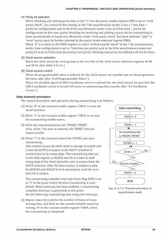
S1C63406/408 TECHNICAL MANUAL EPSON 89
CHAPTER 4: PERIPHERAL CIRCUITS AND OPERATION (Serial Interface)
(4) Parity bit selectionWhen checking and adding parity bits, write "1" into the parity enable register EPR to set to "withparity check". As a result of this setting, in the 7-bit asynchronous mode, it has a 7 bits data +parity bit configuration and in the 8-bit asynchronous mode it has an 8 bits data + parity bitconfiguration.In this case, parity checking for receiving and adding a party bit for transmitting isdone automatically in hardware. Moreover, when "with parity check" has been selected, "odd" or"even" parity must be further selected in the parity mode selection register PMD.When "0" is written to the PMD register to select "without parity check" in the 7-bit asynchronousmode, data configuration is set to 7 bits data (no parity) and in the 8-bit asynchronous mode (noparity) it is set to 8 bits data (no parity) and parity checking and parity bit adding will not be done.
(5) Clock source selectionSelect the clock source by writing data to the two bits of the clock source selection registers SCS0and SCS1. (See Table 4.11.4.1.)
(6) Clock source controlWhen the programmable timer is selected for the clock source, set transfer rate on the programma-ble timer side. (See "4.10 Programmable Timer".)When the divided signal of OSC3 oscillation circuit is selected for the clock source, be sure that theOSC3 oscillation circuit is turned ON prior to commencing data transfer. (See "4.3 OscillationCircuit".)
Data transmit procedureThe control procedure and operation during transmitting is as follows.
(1) Write "0" in the transmit enable register TXEN to reset theserial interface.
(2) Write "1" in the transmit enable register TXEN to set intothe transmitting enable status.
(3) Write the transmitting data into TRXD0–TRXD7.Also, when 7-bit data is selected, the TRXD7 data be-comes invalid.
(4) Write "1" in the transmit control bit TXTRG and starttransmitting.This control causes the shift clock to change to enable anda start bit (LOW) is output to the SOUT terminal insynchronize to its rising edge. The transmitting data setto the shift register is shifted one bit at a time at eachrising edge of the clock thereafter and is output from theSOUT terminal. After the data output, it outputs a stopbit (HIGH) and HIGH level is maintained until the nextstart bit is output.
The transmitting complete interrupt factor flag ISTR is setto "1" at the point where the data transmitting is com-pleted. When interrupt has been enabled, a transmittingcomplete interrupt is generated at this point.Set the following transmitting data using this interrupt.
(5) Repeat steps (3) to (4) for the number of bytes of trans-mitting data, and then set the transmit disable status bywriting "0" to the transmit enable register TXEN, whenthe transmitting is completed.
Data transmitting
End
TXEN ← 0
No
Yes
Transmit complete ?
Set transmitting data
to TRXD0–TRXD7
No
Yes
ISTR = 1 ?
TXEN ← 0
TXTRG ← 1
TXEN ← 1
Fig. 4.11.7.2 Transmit procedure inasynchronous mode
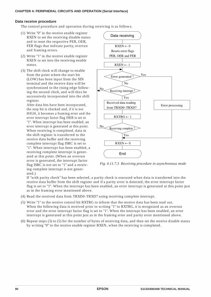
90 EPSON S1C63406/408 TECHNICAL MANUAL
CHAPTER 4: PERIPHERAL CIRCUITS AND OPERATION (Serial Interface)
Data receive procedureThe control procedure and operation during receiving is as follows.
(1) Write "0" in the receive enable registerRXEN to set the receiving disable statusand to reset the respective PER, OER,FER flags that indicate parity, overrunand framing errors.
(2) Write "1" in the receive enable registerRXEN to set into the receiving enablestatus.
(3) The shift clock will change to enablefrom the point where the start bit(LOW) has been input from the SINterminal and the receive data will besynchronized to the rising edge follow-ing the second clock, and will thus besuccessively incorporated into the shiftregister.After data bits have been incorporated,the stop bit is checked and, if it is notHIGH, it becomes a framing error and theerror interrupt factor flag ISER is set to"1". When interrupt has been enabled, anerror interrupt is generated at this point.When receiving is completed, data inthe shift register is transferred to thereceive data buffer and the receivingcomplete interrupt flag ISRC is set to"1". When interrupt has been enabled, areceiving complete interrupt is gener-ated at this point. (When an overrunerror is generated, the interrupt factorflag ISRC is not set to "1" and a receiv-ing complete interrupt is not gener-ated.)
End
RXEN ← 1
No
Yes
Receiving interrupt ?
Yes
Receiving complete ?
Received data reading
from TRXD0–TRXD7
RXEN ← 0
RXTRG ← 1
No
YesError generated ?
Error processing
Data receiving
RXEN ← 0
Resets error flags
PER, OER and FER
No
If "with parity check" has been selected, a parity check is executed when data is transferred into thereceive data buffer from the shift register and if a parity error is detected, the error interrupt factorflag is set to "1". When the interrupt has been enabled, an error interrupt is generated at this point justas in the framing error mentioned above.
(4) Read the received data from TRXD0–TRXD7 using receiving complete interrupt.
(5) Write "1" to the receive control bit RXTRG to inform that the receive data has been read out.When the following data is received prior to writing "1" to RXTRG, it is recognized as an overrunerror and the error interrupt factor flag is set to "1". When the interrupt has been enabled, an errorinterrupt is generated at this point just as in the framing error and parity error mentioned above.
(6) Repeat steps (3) to (5) for the number of bytes of receiving data, and then set the receive disable statusby writing "0" to the receive enable register RXEN, when the receiving is completed.
Fig. 4.11.7.3 Receiving procedure in asynchronous mode

S1C63406/408 TECHNICAL MANUAL EPSON 91
CHAPTER 4: PERIPHERAL CIRCUITS AND OPERATION (Serial Interface)
Receive errorDuring receiving the following three types of errors can be detected by an interrupt.
(1) Parity errorWhen writing "1" to the EPR register to select "with parity check", a parity check (vertical paritycheck) is executed during receiving. After each data bit is sent a parity check bit is sent. The paritycheck bit is a "0" or a "1". Even parity checking will cause the sum of the parity bit and the otherbits to be even. Odd parity causes the sum to be odd. This is checked on the receiving side.The parity check is performed when data received in the shift register is transferred to the receivedata buffer. It checks whether the parity check bit is a "1" or a "0" (the sum of the bits including theparity bit) and the parity set in the PMD register match. When it does not match, it is recognizedas an parity error and the parity error flag PER and the error interrupt factor flag ISER is set to "1".When interrupt has been enabled, an error interrupt is generated at this point.The PER flag is reset to "0" by writing "1".Even when this error has been generated, the received data corresponding to the error is trans-ferred in the receive data buffer and the receive operation also continues.The received data at this point cannot assured because of the parity error.
(2) Framing errorIn asynchronous transfer, synchronization is adopted for each character at the start bit ("0") andthe stop bit ("1"). When receiving has been done with the stop bit set at "0", the serial interfacejudges the synchronization to be off and a framing error is generated. When this error is gener-ated, the framing error flag FER and the error interrupt factor flag ISER are set to "1". Wheninterrupt has been enabled, an error interrupt is generated at this point.The FER flag is reset to "0" by writing "1".Even when this error has been generated, the received data for it is loaded into the receive databuffer and the receive operation also continues. However, even when it does not become a framingerror with the following data receipt, such data cannot be assured.Even when this error has been generated, the received data corresponding to the error is trans-ferred in the receive data buffer and the receive operation also continues. However, even when itdoes not become a framing error with the following data receiving, such data cannot be assured.
(3) Overrun errorWhen the next data is received before "1" is written to RXTRG, an overrun error will be generated,because the previous receive data will be overwritten. When this error is generated, the overrunerror flag OER and the error interrupt factor flag ISER are set to "1". When interrupt has beenenabled, an error interrupt is generated at this point. The OER flag is reset to "0" by writing "1"into it.Even when this error has been generated, the received data corresponding to the error is trans-ferred in the receive data buffer and the receive operation also continues.Furthermore, when the timing for writing "1" to RXTRG and the timing for the received datatransfer to the receive data buffer overlap, it will be recognized as an overrun error.
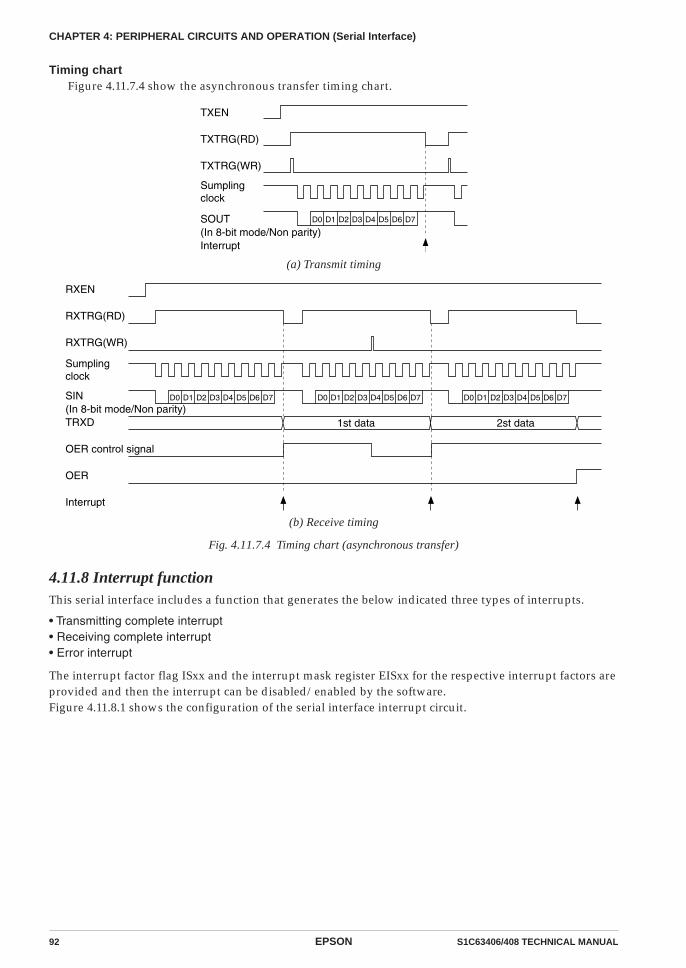
92 EPSON S1C63406/408 TECHNICAL MANUAL
CHAPTER 4: PERIPHERAL CIRCUITS AND OPERATION (Serial Interface)
Timing chartFigure 4.11.7.4 show the asynchronous transfer timing chart.
TXEN
TXTRG(RD)
TXTRG(WR)
SOUT
Interrupt(In 8-bit mode/Non parity)
D0 D1 D2 D3 D4 D5 D6 D7
Sumplingclock
(a) Transmit timing
RXEN
RXTRG(RD)
RXTRG(WR)
SIN
TRXD
OER control signal
OER
Interrupt
(In 8-bit mode/Non parity)D0 D1 D2 D3 D4 D5 D6 D7 D0 D1 D6 D7 D0 D1 D2 D3 D4 D5 D6 D7D2 D3 D4 D5
1st data 2st data
Sumplingclock
(b) Receive timing
Fig. 4.11.7.4 Timing chart (asynchronous transfer)
4.11.8 Interrupt functionThis serial interface includes a function that generates the below indicated three types of interrupts.
• Transmitting complete interrupt• Receiving complete interrupt• Error interrupt
The interrupt factor flag ISxx and the interrupt mask register EISxx for the respective interrupt factors areprovided and then the interrupt can be disabled/enabled by the software.Figure 4.11.8.1 shows the configuration of the serial interface interrupt circuit.
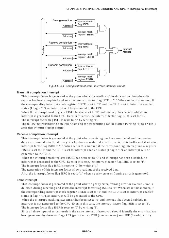
S1C63406/408 TECHNICAL MANUAL EPSON 93
CHAPTER 4: PERIPHERAL CIRCUITS AND OPERATION (Serial Interface)
Dat
a bu
s
Interruptrequest
Address
Error generation Interrupt factorflag ISER
Address
Interrupt maskregister EISER
Address
Receive completion Interrupt factorflag ISRC
Address
Interrupt maskregister EISRC
Address
Transmit completion Interrupt factorflag ISTR
Address
Interrupt maskregister EISTR
Fig. 4.11.8.1 Configuration of serial interface interrupt circuit
Transmit completion interruptThis interrupt factor is generated at the point where the sending of the data written into the shiftregister has been completed and sets the interrupt factor flag ISTR to "1". When set in this manner, ifthe corresponding interrupt mask register EISTR is set to "1" and the CPU is set to interrupt enabledstatus (I flag = "1"), an interrupt will be generated to the CPU.When the interrupt mask register EISTR has been set to "0" and interrupt has been disabled, nointerrupt is generated to the CPU. Even in this case, the interrupt factor flag ISTR is set to "1".The interrupt factor flag ISTR is reset to "0" by writing "1".The following transmitting data can be set and the transmitting can be started (writing "1" to TXTRG)after this interrupt factor occurs.
Receive completion interruptThis interrupt factor is generated at the point where receiving has been completed and the receivedata incorporated into the shift register has been transferred into the receive data buffer and it sets theinterrupt factor flag ISRC to "1". When set in this manner, if the corresponding interrupt mask registerEISRC is set to "1" and the CPU is set to interrupt enabled status (I flag = "1"), an interrupt will begenerated to the CPU.When the interrupt mask register EISRC has been set to "0" and interrupt has been disabled, nointerrupt is generated to the CPU. Even in this case, the interrupt factor flag ISRC is set to "1".The interrupt factor flag ISRC is reset to "0" by writing "1".The generation of this interrupt factor allows reading of the received data.Also, the interrupt factor flag ISRC is set to "1" when a parity error or framing error is generated.
Error interruptThis interrupt factor is generated at the point where a parity error, framing error or overrun error isdetected during receiving and it sets the interrupt factor flag ISER to "1". When set in this manner, ifthe corresponding interrupt mask register EISER is set to "1" and the CPU is set to interrupt enabledstatus (I flag = "1"), an interrupt will be generated to the CPU.When the interrupt mask register EISER has been set to "0" and interrupt has been disabled, aninterrupt is not generated to the CPU. Even in this case, the interrupt factor flag ISER is set to "1".The interrupt factor flag ISER is reset to "0" by writing "1".Since all three types of errors result in the same interrupt factor, you should identify the error that hasbeen generated by the error flags PER (parity error), OER (overrun error) and FER (framing error).
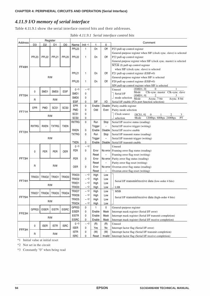
94 EPSON S1C63406/408 TECHNICAL MANUAL
CHAPTER 4: PERIPHERAL CIRCUITS AND OPERATION (Serial Interface)
4.11.9 I/O memory of serial interfaceTable 4.11.9.1 show the serial interface control bits and their addresses.
Table 4.11.9.1 Serial interface control bits
Address CommentD3 D2
Register
D1 D0 Name Init ∗1 1 0
0Clk-sync. master
2Async. 7-bit
1Clk-sync. slave
3Async. 8-bit
[SMD1, 0]Mode[SMD1, 0]Mode
FF70H0 SMD1 SMD0 ESIF
R R/W
0 ∗3
SMD1SMD0ESIF
– ∗2
000 SIF I/O
Unused
Serial I/F
mode selection
Serial I/F enable (P2x port function selection)
01200bps
1600bps
22400bps
3PT
[SCS1, 0]Mode
FF71HEPR PMD SCS1 SCS0
R/W
EPRPMDSCS1SCS0
0000
EnableOdd
DisableEven
Parity enable register
Parity mode selection
Clock source
selection
R/W
FF72H
RXTRG RXEN TXTRG TXENRXTRG
RXENTXTRG
TXEN
0
00
0
RunTriggerEnable
RunTriggerEnable
Stop–
DisableStop
–Disable
Serial I/F receive status (reading)
Serial I/F receive trigger (writing)
Serial I/F receive enable
Serial I/F transmit status (reading)
Serial I/F transmit trigger (writing)
Serial I/F transmit enable
R R/W
FF73H
0 FER PER OER
0 ∗3
FER
PER
OER
– ∗2
0
0
0
ErrorResetErrorResetErrorReset
No error–
No error–
No error–
Unused
Framing error flag status (reading)
Framing error flag reset (writing)
Parity error flag status (reading)
Parity error flag reset (writing)
Overrun error flag status (reading)
Overrun error flag reset (writing)
R/W
FF74HTRXD3 TRXD2 TRXD1 TRXD0
TRXD3TRXD2TRXD1TRXD0
– ∗2
– ∗2
– ∗2
– ∗2
HighHighHighHigh
LowLowLowLow
Serial I/F transmit/receive data (low-order 4 bits)
LSB
R/W
FF75HTRXD7 TRXD6 TRXD5 TRXD4
TRXD7TRXD6TRXD5TRXD4
– ∗2
– ∗2
– ∗2
– ∗2
HighHighHighHigh
LowLowLowLow
MSB
Serial I/F transmit/receive data (high-order 4 bits)
FFF3H0 ISER ISTR ISRC
R R/W
0 ∗3
ISERISTRISRC
– ∗2
000
(R)Yes(W)
Reset
(R)No(W)
Invalid
Unused
Interrupt factor flag (Serial I/F error)
Interrupt factor flag (Serial I/F transmit completion)
Interrupt factor flag (Serial I/F receive completion)
FF49H
PPL23 PPL22 PPL21 PPL20
R/W
PPL23
PPL22
PPL21
PPL20
1
1
1
1
On
On
On
On
Off
Off
Off
Off
P23 pull-up control register
General-purpose register when SIF (clock sync. slave) is selected
P22 pull-up control register
General-purpose register when SIF (clock sync. master) is selected
SCLK (I) pull-up control register
when SIF (clock sync. slave) is selected
P21 pull-up control register (ESIF=0)
General-purpose register when SIF is selected
P20 pull-up control register (ESIF=0)
SIN pull-up control register when SIF is selected
FFE3HGPR33 EISER EISTR EISRC
R/W
GPR33EISEREISTREISRC
0000
1EnableEnableEnable
0MaskMaskMask
General-purpose register
Interrupt mask register (Serial I/F error)
Interrupt mask register (Serial I/F transmit completion)
Interrupt mask register (Serial I/F receive completion)
*1 Initial value at initial reset
*2 Not set in the circuit
*3 Constantly "0" when being read

S1C63406/408 TECHNICAL MANUAL EPSON 95
CHAPTER 4: PERIPHERAL CIRCUITS AND OPERATION (Serial Interface)
ESIF: Serial interface enable register (P2 port function selection) (FF70H•D0)Sets P20–P23 to the input/output port for the serial interface.
When "1" is written: Serial interfaceWhen "0" is written: I/O port
Reading: Valid
The ESIF is the serial interface enable register and P20–P23 terminals become serial input/output termi-nals (SIN, SOUT, SCLK, SRDY) when "1" is written, and they become I/O port terminals when "0" iswritten.Also, see Table 4.11.3.2 for the terminal settings according to the transfer modes.At initial reset, this register is set to "0".
PPL20: SIN pull-up control register (FF49H•D0)PPL22: SCLK pull-up control register (FF49H•D2)Sets the pull-up of the SIN terminal and the SCLK terminals (in the slave mode).
When "1" is written: Pull-up ONWhen "0" is written: Pull-up OFF
Reading: Valid
Sets the pull-up resistor built into the SIN (P20) and SCLK (P22) terminals to ON or OFF.SCLK pull-up is effective only in the slave mode. In the master mode, the PPL22 register can be used as ageneral purpose register.At initial reset, these registers are set to "1" and the lines are pulled up.
SMD0, SMD1: Serial interface mode selection register (FF70H•D1, D2)Set the transfer modes as shown in Table 4.11.9.2.
Table 4.11.9.2 Transfer mode settings
SMD1 SMD0 Mode
1
1
0
0
1
0
1
0
8-bit asynchronous
7-bit asynchronous
Clock synchronous slave
Clock synchronous master
SMD0 and SMD1 can also read out.At initial reset, this register is set to "0".
SCS0, SCS1: Clock source selection register (FF71H•D0, D1)Select the clock source as shown in Table 4.11.9.3.
Table 4.11.9.3 Clock source selection
SCS1
1
1
0
0
SCS0
1
0
1
0
Clock source
Programmable timer
fOSC3 / 93
fOSC3 / 372
fOSC3 / 186
SCS0 and SCS1 can also be read out.In the clock synchronous slave mode, setting of this register is invalid.At initial reset, this register is set to "0".
96 EPSON S1C63406/408 TECHNICAL MANUAL
CHAPTER 4: PERIPHERAL CIRCUITS AND OPERATION (Serial Interface)
EPR: Parity enable register (FF71H•D3)Selects the parity function.
When "1" is written: With parityWhen "0" is written: Non parity
Reading: Valid
Selects whether or not to check parity of the received data and to add a parity bit to the transmitting data.When "1" is written to EPR, the most significant bit of the received data is considered to be the parity bitand a parity check is executed. A parity bit is added to the transmitting data. When "0" is written, neitherchecking is done nor is a parity bit added.Parity is valid only in asynchronous mode and the EPR setting becomes invalid in the clock synchronousmode.At initial reset, this register is set to "0".
PMD: Parity mode selection register (FF71H•D2)Selects odd parity/even parity.
When "1" is written: Odd parityWhen "0" is written: Even parity
Reading: Valid
When "1" is written to PMD, odd parity is selected and even parity is selected when "0" is written. Theparity check and addition of a parity bit is only valid when "1" has been written to EPR. When "0" hasbeen written to EPR, the parity setting by PMD becomes invalid.At initial reset, this register is set to "0".
TXEN: Transmit enable register (FF72H•D0)Sets the serial interface to the transmit enabled status.
When "1" is written: Transmit enabledWhen "0" is written: Transmit disabled
Reading: Valid
When "1" is written to TXEN, the serial interface shifts to the transmit enabled status and shifts to thetransmit disabled status when "0" is written.Set TXEN to "0" when making the initial settings of the serial interface and similar operations.At initial reset, this register is set to "0".
TXTRG: Transmit trigger/status (FF72H•D1)Functions as the transmit start trigger and the operation status indicator (transmitting/stop status).
When "1" is read: During transmittingWhen "0" is read: During stop
When "1" is written: Start transmittingWhen "0" is written: Invalid
Starts transmitting when "1" is written to TXTRG after writing the transmitting data.TXTRG can be read as the status. When set to "1", it indicates transmitting operation, and "0" indicatestransmitting stop.At initial reset, TXTRG is set to "0".
S1C63406/408 TECHNICAL MANUAL EPSON 97
CHAPTER 4: PERIPHERAL CIRCUITS AND OPERATION (Serial Interface)
RXEN: Receive enable register (FF72H•D2)Sets the serial interface to the receive enabled status.
When "1" is written: Receive enabledWhen "0" is written: Receive disabled
Reading: Valid
When "1" is written to RXEN, the serial interface shifts to the receive enabled status and shifts to thereceive disabled status when "0" is written.Set RXEN to "0" when making the initial settings of the serial interface and similar operations.At initial reset, this register is set to "0".
RXTRG: Receive trigger/status (FF72H•D3)Functions as the receive start trigger or preparation for the following data receiving and the operationstatus indicator (during receiving/during stop).
When "1" is read: During receivingWhen "0" is read: During stop
When "1" is written: Start receiving/following data receiving preparationWhen "0" is written: Invalid
RXTRG has a slightly different operation in the clock synchronous system and the asynchronous system.
The RXTRG in the clock synchronous system is used as the trigger for starting receive operation.Write "1" into RXTRG to start receiving at the point where the receive data has been read and thefollowing receive preparation has been done. (In the slave mode, SRDY becomes "0" at the point where"1" has been written into into the RXTRG.)
In the asynchronous system, RXTRG is used for preparation of the following data receiving. Read thereceived data located in the receive data buffer and write "1" into RXTRG to inform that the receive databuffer has shifted to empty. When "1" has not been written to RXTRG, the overrun error flag OER is set to"1" at the point where the following receiving has been completed. (When the receiving has been com-pleted between the operation to read the received data and the operation to write "1" into RXTRG, anoverrun error occurs.)
In addition, RXTRG can be read as the status. In either clock synchronous mode or asynchronous mode,when RXTRG is set to "1", it indicates receiving operation and when set to "0", it indicates that receivinghas stopped.At initial reset, RXTRG is set to "0".
TRXD0–TRXD7: Transmit/receive data (FF74H, FF75H)
During transmitting
Transmitting data is set.
When "1" is written: High levelWhen "0" is written: Low level
Write the transmitting data prior to starting transmition.In the case of continuous transmitting, wait for the transmit completion interrupt, then write the data.The TRXD7 becomes invalid for the 7-bit asynchronous mode.Converted serial data for which the bits set at "1" as High (VDD) level and for which the bits set at "0" asLow (VSS) level are output from the SOUT terminal.
During receiving
The received data is stored.
When "1" is read: High levelWhen "0" is read: Low level
The data from the receive data buffer can be read out.Since the sift register is provided separately from this buffer, reading can be done during a receive opera-tion in the asynchronous mode. (The buffer function is not used in the clock synchronous mode.)

98 EPSON S1C63406/408 TECHNICAL MANUAL
CHAPTER 4: PERIPHERAL CIRCUITS AND OPERATION (Serial Interface)
Read the data after waiting for a receive completion interrupt.When performing parity check in the 7-bit asynchronous mode, "0" is loaded into the 8th bit (TRXD7) thatcorresponds to the parity bit.The serial data input from the SIN terminal is level converted, making the High (VDD) level bit "1" andthe Low (VSS) level bit "0" and is then loaded into this buffer.At initial reset, the buffer content is undefined.
OER: Overrun error flag (FF73H•D0)Indicates the generation of an overrun error.
When "1" is read: ErrorWhen "0" is read: No error
When "1" is written: Reset to "0"When "0" is written: Invalid
OER is an error flag that indicates the generation of an overrun error and becomes "1" when an error hasbeen generated.An overrun error is generated when a receiving of data has completed prior to writing "1" to RXTRG inthe asynchronous mode.OER is reset to "0" by writing "1".OER is set to "0" at initial reset or when RXEN is set to "0".
PER: Parity error flag (FF73H•D1)Indicates the generation of a parity error.
When "1" is read: ErrorWhen "0" is read: No error
When "1" is written: Reset to "0"When "0" is written: Invalid
PER is an error flag that indicates the generation of a parity error and becomes "1" when an error has beengenerated.When a parity check is performed in the asynchronous mode, a parity error will be generated if data thatdoes not match the parity is received.PER is reset to "0" by writing "1".PER is set to "0" at initial reset or when RXEN is set to "0".
FER: Framing error flag (FF73H•D2)Indicates the generation of a framing error.
When "1" is read: ErrorWhen "0" is read: No error
When "1" is written: Reset to "0"When "0" is written: Invalid
FER is an error flag that indicates the generation of a framing error and becomes "1" when an error hasbeen generated.When the stop bit for the receiving in the asynchronous mode has become "0", a framing error is gener-ated.FER is reset to "0" by writing "1".FER is set to "0" at initial reset or when RXEN is set to "0".
S1C63406/408 TECHNICAL MANUAL EPSON 99
CHAPTER 4: PERIPHERAL CIRCUITS AND OPERATION (Serial Interface)
EISRC, EISTR, EISER: Interrupt mask registers (FFE3H•D0, D1, D2)Enables or disables the generation of an interrupt for the CPU.
When "1" is written: EnabledWhen "0" is written: Disabled
Reading: Valid
EISRC, EISTR and EISER are interrupt mask registers that respectively correspond to the interrupt factorsfor receivie completion, transmit completion and receive error. Interrupts set to "1" are enabled andinterrupts set to "0" are disabled.At initial reset, these registers are set to "0".
ISRC, ISTR, ISER: Interrupt factor flags (FFF3H•D0, D1, D2)Indicates the serial interface interrupt generation status.
When "1" is read: Interrupt has occurredWhen "0" is read: Interrupt has not occurred
When "1" is written: Flag is resetWhen "0" is written: Invalid
ISRC, ISTR and ISER are interrupt factor flags that respectively correspond to the interrupts for receiviecompletion, transmit completion and receive error, and are set to "1" by generation of each factor.Transmit completion interrupt factor is generated at the point where the data transmition of the shiftregister has been completed.Receive completion interrupt factor is generated at the point where the received data has been transferredinto the receive data buffer.Receive error interrupt factor is generated when a parity error, framing error or overrun error has beendetected during data receiving.When set in this manner, if the corresponding interrupt enable mask is set to "1" and the CPU is set tointerrupt enabled status (I flag = "1"), an interrupt will be generated to the CPU.Regardless of the interrupt mask register setting, the interrupt factor flag will be set to "1" by the occurrenceof an interrupt generation condition.The interrupt factor flag is reset to "0" by writing "1".After an interrupt occurs, the same interrupt will occur again if the interrupt enabled state (I flag = "1") isset or the RETI instruction is executed unless the interrupt factor flag is reset. Therefore, be sure to reset(write "1" to) the interrupt factor flag in the interrupt service routine before shifting to the interruptenabled state.At initial reset, these flags are set to "0".
100 EPSON S1C63406/408 TECHNICAL MANUAL
CHAPTER 4: PERIPHERAL CIRCUITS AND OPERATION (Serial Interface)
4.11.10 Programming notes(1) Be sure to initialize the serial interface mode in the transmit/receive disabled status (TXEN = RXEN =
"0").
(2) Do not perform double trigger (writing "1") to TXTRG (RXTRG) when the serial interface is in thetransmitting (receiving) operation.
(3) In the clock synchronous mode, since one clock line (SCLK) is shared for both transmitting andreceiving, transmitting and receiving cannot be performed simultaneously. (Half duplex only ispossible in clock synchronous mode.)Consequently, be sure not to write "1" to RXTRG (TXTRG) when TXTRG (RXTRG) is "1".
(4) When a parity error or flaming error is generated during receiving in the asynchronous mode, thereceiving error interrupt factor flag ISER is set to "1" prior to the receive completion interrupt factorflag ISRC for the time indicated in Table 4.11.10.1. Consequently, when an error is generated, youshould reset the receiving complete interrupt factor flag ISRC to "0" by providing a wait time in errorprocessing routines and similar routines.When an overrun error is generated, the receiving complete interrupt factor flag ISRC is not set to "1"and a receiving complete interrupt is not generated.
Table 4.11.10.1 Time difference between ISER and ISRC on error generation
Clock source Time difference
fOSC3 / n
Programmable timer
1/2 cycles of fOSC3 / n
1 cycle of timer 1 underflow
(5) When the demultiplied signal of the OSC3 oscillation circuit is made the clock source, it is necessaryto turn the OSC3 oscillation ON, prior to using the serial interface.A time interval of 5 msec, from the turning ON of the OSC3 oscillation circuit to until the oscillationstabilizes, is necessary, due to the oscillation element that is used. Consequently, you should allow anadequate waiting time after turning ON of the OSC3 oscillation, before starting transmitting/receiv-ing of serial interface. (The oscillation start time will vary somewhat depending on the oscillator andon the externally attached parts. Refer to the oscillation start time example indicated in Chapter 7,"Electrical Chracteristics".)At initial reset, the OSC3 oscillation circuit is set to OFF status.
(6) Be aware that the maximum clock frequency for the serial interface is limited to 2 MHz.
(7) After an interrupt occurs, the same interrupt will occur again if the interrupt enabled state (I flag ="1") is set or the RETI instruction is executed unless the interrupt factor flag is reset. Therefore, be sureto reset (write "1" to) the interrupt factor flag in the interrupt service routine before shifting to theinterrupt enabled state.

S1C63406/408 TECHNICAL MANUAL EPSON 101
CHAPTER 4: PERIPHERAL CIRCUITS AND OPERATION (SVD Circuit)
4.12 SVD (Supply Voltage Detection) Circuit
4.12.1 Configuration of SVD circuitThe S1C63406/408 has a built-in SVD (supply voltage detection) circuit, so that the software can findwhen the source voltage lowers.Turning the SVD circuit ON/OFF and the SVD criteria voltage setting can be done with software.Figure 4.12.1.1 shows the configuration of the SVD circuit.
V
Detection output
Dat
a bu
s
DD
VSS
SVDON
SVDS3|
SVDS0
Criteria voltagesetting circuit
SVD circuit SVDDT
Fig. 4.12.1.1 Configuration of SVD circuit
4.12.2 SVD operationThe SVD circuit compares the criteria voltage set by software and the supply voltage (VDD terminal–VSS
terminal) and sets its results into the SVDDT latch. By reading the data of this SVDDT latch, it can bedetermined by means of software whether the supply voltage is normal or has dropped.The criteria voltage can be set for the 16 types shown in Table 4.12.2.1 by the SVDS3–SVDS0 registers.When "0" is written to the SVDS3–SVDS0 register, the supply voltage detection voltage is set to 1.30 V.When "8" is written to the SVDS3–SVDS0 register, it is set to 2.10 V.
Table 4.12.2.1 Criteria voltage setting
SVDS3
0
0
0
0
0
0
0
0
SVDS2
1
1
1
1
0
0
0
0
SVDS1
1
1
0
0
1
1
0
0
SVDS0
1
0
1
0
1
0
1
0
Criteriavoltage (V)
2.00
1.90
1.80
1.70
1.60
1.50
1.40
1.30
SVDS3
1
1
1
1
1
1
1
1
SVDS2
1
1
1
1
0
0
0
0
SVDS1
1
1
0
0
1
1
0
0
SVDS0
1
0
1
0
1
0
1
0
Criteriavoltage (V)
2.80
2.70
2.60
2.50
2.40
2.30
2.20
2.10
When the SVDON register is set to "1", source voltage or external voltage detection by the SVD circuit isexecuted. As soon as the SVDON register is reset to "0", the result is loaded to the SVDDT latch and theSVD circuit goes OFF.To obtain a stable detection result, the SVD circuit must be ON for at least l00 µsec. So, to obtain the SVDdetection result, follow the programming sequence below.
1. Set SVDON to "1"2. Maintain for 100 µsec minimum3. Set SVDON to "0"4. Read SVDDT
When the SVD circuit is ON, the IC draws a large current, so keep the SVD circuit off unless it is.

102 EPSON S1C63406/408 TECHNICAL MANUAL
CHAPTER 4: PERIPHERAL CIRCUITS AND OPERATION (SVD Circuit)
4.12.3 I/O memory of SVD circuitTable 4.12.3.1 shows the I/O addresses and the control bits for the SVD circuit.
Table 4.12.3.1 Control bits of SVD circuit
Address CommentD3 D2
Register
D1 D0 Name Init ∗1 1 0
FF05H0 0 SVDDT SVDON
R R/W
0 ∗3
0 ∗3
SVDDTSVDON
– ∗2
– ∗2
00
LowOn
NormalOff
Unused
Unused
SVD evaluation data
SVD circuit On/Off
FF04HSVDS3 SVDS2 SVDS1 SVDS0
R/W
SVDS3SVDS2SVDS1SVDS0
0000
SVD criteria voltage setting0
1.308
2.10
11.40
92.20
21.5010
2.30
31.6011
2.40
41.7012
2.50
51.8013
2.60
61.9014
2.70
72.0015
2.80
[SVDS3–0]Voltage(V)[SVDS3–0]Voltage(V)
*1 Initial value at initial reset
*2 Not set in the circuit
*3 Constantly "0" when being read
SVDS3–SVDS0: SVD criteria voltage setting register (FF04H)Criteria voltage for SVD is set as shown in Table 4.12.2.1.At initial reset, this register is set to "0".
SVDON: SVD control (ON/OFF) register (FF05H•D0)Turns the SVD circuit ON and OFF.
When "1" is written: SVD circuit ONWhen "0" is written: SVD circuit OFF
Reading: Valid
When the SVDON register is set to "1", a source voltage detection is executed by the SVD circuit. As soonas SVDON is reset to "0", the result is loaded to the SVDDT latch. To obtain a stable detection result, theSVD circuit must be ON for at least l00 µsec.At initial reset, this register is set to "0".
SVDDT: SVD data (FF05H•D1)This is the result of supply voltage detection.
When "0" is read: Supply voltage (VDD–VSS) ≥ Criteria voltageWhen "1" is read: Supply voltage (VDD–VSS) < Criteria voltage
Writing: Invalid
The result of supply voltage detection at time of SVDON is set to "0" can be read from this latch.At initial reset, SVDDT is set to "0".
4.12.4 Programming notes(1) To obtain a stable detection result, the SVD circuit must be ON for at least l00 µsec. So, to obtain the
SVD detection result, follow the programming sequence below.
1. Set SVDON to "1"2. Maintain for 100 µsec minimum3. Set SVDON to "0"4. Read SVDDT
(2) The SVD circuit should normally be turned OFF because SVD operation increase current consump-tion.
S1C63406/408 TECHNICAL MANUAL EPSON 103
CHAPTER 4: PERIPHERAL CIRCUITS AND OPERATION (Heavy Load Protection Function)
4.13 Heavy Load Protection Function
4.13.1 Outline of heavy load protection functionThe S1C63406/408 has a heavy load protection function for when the battery load becomes heavy, such aswhen an external lamp is lit or the buzzer is on (piezoelectric buzzer is driven). In such case, the heavyload protection function is suitable.The normal mode (heavy load protection function is off) changes to the heavy load protection mode(heavy load protection function is on) when the software changes the mode to the heavy load protectionmode (HLMOD = "1").
Note: In the heavy load protection mode, more current is consumed than in the normal mode. Unlessnecessary, do not select the heavy load protection mode with the software.
4.13.2 I/O memory of heavy load protection functionTable 4.13.2.1 shows the I/O address and the control bit for the heavy load protection function.
Table 4.13.2.1 Control bit of heavy load protection function
Address CommentD3 D2
RegisterD1 D0 Name Init ∗1 1 0
FF07HHLMOD 0 WDEN WDRST
R/W R R/W W
HLMOD 0 ∗3
WDENWDRST∗3
0 – ∗2
1Reset
On
EnableReset
Off
DisableInvalid
Heavy load protection
Unused
Watchdog timer enable
Watchdog timer reset (writing)
*1 Initial value at initial reset
*2 Not set in the circuit
*3 Constantly "0" when being read
HLMOD: Heavy load protection (FF07H•D3)Heavy load protection On/Off is controlled with this register.
When "1" is written: Heavy load protection onWhen "0" is written: Heavy load protection off
Reading: Valid
The device enters the heavy load protection mode by writing "1" to HLMOD, and returns to the normalmode by writing "0".At initial reset, this register is set to "0".
4.13.3 Programming noteBe aware that current consumption increases in the heavy load protection mode.

104 EPSON S1C63406/408 TECHNICAL MANUAL
CHAPTER 4: PERIPHERAL CIRCUITS AND OPERATION (Interrupt and HALT/SLEEP)
4.14 Interrupt and HALT/SLEEP
<Interrupt types>The S1C63406/408 provides the following interrupt functions.
External interrupt: • Input port interrupt (4 systems)
Internal interrupt: • Watchdog timer interrupt (NMI, 1 system)• Programmable timer interrupt (2 systems)• Serial interface interrupt (3 systems)• Timer interrupt (4 systems)• Stopwatch timer interrupt (2 systems)
To authorize interrupt, the interrupt flag must be set to "1" (EI) and the necessary related interrupt maskregisters must be set to "1" (enable).When an interrupt occurs the interrupt flag is automatically reset to "0" (DI), and interrupts after that areinhibited.
The watchdog timer interrupt is an NMI (non-maskable interrupt), therefore, the interrupt is generatedregardless of the interrupt flag setting. Also the interrupt mask register is not provided. However, it ispossible to not generate NMI since software can stop the watchdog timer operation.
Figure 4.14.1 shows the configuration of the interrupt circuit.
Note: After an initial reset, all the interrupts including NMI are masked until both the stack pointers SP1and SP2 are set with the software. Be sure to set the SP1 and SP2 in the initialize routine.Further, when re-setting the stack pointer, the SP1 and SP2 must be set as a pair. When one ofthem is set, all the interrupts including NMI are masked and interrupts cannot be accepted until theother one is set.
<HALT/SLEEP>The S1C63406/408 has HALT and SLEEP functions that considerably reduce current consumption whenit is not necessary.The CPU enters HALT status when the HALT instruction is executed.In HALT status, the operation of the CPU is stopped. However, timers continue counting since theoscillation circuit operates. Reactivating the CPU from HALT status is done by generating a hardwareinterrupt request including NMI.When the CPU enters SLEEP status as the result of the SLP instruction, the CPU stops its operation, theOSC3 oscillation circuit and supplying the OSC1 clock to the divider and peripheral circuits. However,the OSC1 oscillation circuit does not stop its oscillation.Reactivating from SLEEP status can only be done by generation of an input port interrupt factor. There-fore, set the following flag and the registers for the K0x port to be used to cancel SLEEP status beforeexecuting the SLP instruction.• Interrupt flag (I flag) = "1" (interrupts are enabled)• Interrupt selection register SIK0x = "1" (the K0x input port interrupt is selected)• Interrupt mask register EIK0x = "1" (the K0x input port interrupt is enabled)• Noise rejector selection register K0NR1–K0NR0 = "00" (noise rejector is bypassed)
When SLEEP status is canceled by an input interrupt, wait for oscillation to stabilize, then restart the CPUoperation (input port interrupt processing).Refer to the "S1C63000 Core CPU Manual" for transition to the HALT/SLEEP status and timing of itscancellation.

S1C63406/408 TECHNICAL MANUAL EPSON 105
CHAPTER 4: PERIPHERAL CIRCUITS AND OPERATION (Interrupt and HALT/SLEEP)
Fig. 4.14.1 Configuration of the interrupt circuit
K00
KCP00
SIK00
K01
KCP01
SIK01
K02
KCP02
SIK02
K03
KCP03
SIK03
IT3
EIT3
IT2
EIT2
IT1
EIT1
IT0
EIT0
ISW1
EISW1
ISW10
EISW10
IPT0
EIPT0
IPT1
EIPT1
ISER
EISER
ISRC
EISRC
ISTR
EISTR
Interruptvector
generationcircuit
Programcounter(low-order 4 bits)
INTInterrupt request
SLEEPcancelation
NMI requestWatchdog timer
Interrupt factor flag
Interrupt mask register
Input comparison register
Interrupt selection register
Interrupt flag
IK00
EIK00
IK01
EIK01
IK02
EIK02
IK03
EIK03
106 EPSON S1C63406/408 TECHNICAL MANUAL
CHAPTER 4: PERIPHERAL CIRCUITS AND OPERATION (Interrupt and HALT/SLEEP)
4.14.1 Interrupt factorTable 4.14.1.1 shows the factors for generating interrupt requests.
The interrupt flags are set to "1" depending on the corresponding interrupt factors.The CPU operation is interrupted when an interrupt factor flag is set to "1" if the following conditions areestablished.
• The corresponding mask register is "1" (enabled)• The interrupt flag is "1" (EI)
The interrupt factor flag is reset to "0" when "1" is written.At initial reset, the interrupt factor flags are reset to "0".
∗ Since the watchdog timer's interrupt is NMI, the interrupt is generated regardless of the setting above,and no interrupt factor flag is provided.
Table 4.14.1.1 Interrupt factorsInterrupt factor
Programmable timer 1 (counter = 0)Programmable timer 0 (counter = 0)Serial interface (receive error)Serial interface (receive completion)Serial interface (transmit completion)K03 input (falling edge or rising edge)K02 input (falling edge or rising edge)K01 input (falling edge or rising edge)K00 input (falling edge or rising edge)Clock timer 1 Hz (falling edge)Clock timer 2 Hz (falling edge)Clock timer 8 Hz (falling edge)Clock timer 32 Hz (falling edge)Stopwatch timer (1 Hz)Stopwatch timer (10 Hz)
IPT1IPT0ISERISRCISTRIK03IK02IK01IK00IT3IT2IT1IT0ISW1ISW10
(FFF2H•D1)(FFF2H•D0)(FFF3H•D2)(FFF3H•D0)(FFF3H•D1)(FFFBH•D3)(FFFBH•D2)(FFFBH•D1)(FFFBH•D0)(FFF6H•D3)(FFF6H•D2)(FFF6H•D1)(FFF6H•D0)(FFF7H•D1)(FFF7H•D0)
Interrupt factor flag
Note: After an interrupt occurs, the same interrupt will occur again if the interrupt enabled state (I flag ="1") is set or the RETI instruction is executed unless the interrupt factor flag is reset. Therefore, besure to reset (write "1" to) the interrupt factor flag in the interrupt service routine before shifting tothe interrupt enabled state.

S1C63406/408 TECHNICAL MANUAL EPSON 107
CHAPTER 4: PERIPHERAL CIRCUITS AND OPERATION (Interrupt and HALT/SLEEP)
4.14.2 Interrupt maskThe interrupt factor flags can be masked by the corresponding interrupt mask registers.The interrupt mask registers are read/write registers. They are enabled (interrupt authorized) when "1" iswritten to them, and masked (interrupt inhibited) when "0" is written to them.At initial reset, the interrupt mask register is set to "0".Table 4.14.2.1 shows the correspondence between interrupt mask registers and interrupt factor flags.
Table 4.14.2.1 Interrupt mask registers and interrupt factor flags
IPT1IPT0ISERISRCISTRIK03IK02IK01IK00IT3IT2IT1IT0ISW1ISW10
(FFF2H•D1)(FFF2H•D0)(FFF3H•D2)(FFF3H•D0)(FFF3H•D1)(FFFBH•D3)(FFFBH•D2)(FFFBH•D1)(FFFBH•D0)(FFF6H•D3)(FFF6H•D2)(FFF6H•D1)(FFF6H•D0)(FFF7H•D1)(FFF7H•D0)
Interrupt factor flagEIPT1EIPT0EISEREISRCEISTREIK03EIK02EIK01EIK00EIT3EIT2EIT1EIT0EISW1EISW10
(FFE2H•D1)(FFE2H•D0)(FFE3H•D2)(FFE3H•D0)(FFE3H•D1)(FFEBH•D3)(FFEBH•D2)(FFEBH•D1)(FFEBH•D0)(FFE6H•D3)(FFE6H•D2)(FFE6H•D1)(FFE6H•D0)(FFE7H•D1)(FFE7H•D0)
Interrupt mask register
4.14.3 Interrupt vectorWhen an interrupt request is input to the CPU, the CPU begins interrupt processing. After the programbeing executed is terminated, the interrupt processing is executed in the following order.
1 The content of the flag register is evacuated, then the I flag is reset.
2 The address data (value of program counter) of the program to be executed next is saved in the stackarea (RAM).
3 The interrupt request causes the value of the interrupt vector (0100H–010AH) to be set in the programcounter.
4 The program at the specified address is executed (execution of interrupt processing routine bysoftware).
Table 4.14.3.1 shows the correspondence of interrupt requests and interrupt vectors.
Table 4.14.3.1 Interrupt request and interrupt vectors
Interrupt vector0100H
0102H
0104H
0106H
0108H
010AH
Interrupt factorWatchdog timer
Programmable timer
Serial interface
K00–K03 input
Clock timer
Stopwatch timer
PriorityHigh
Low
The four low-order bits of the program counter are indirectly addressed through the interrupt request.

108 EPSON S1C63406/408 TECHNICAL MANUAL
CHAPTER 4: PERIPHERAL CIRCUITS AND OPERATION (Interrupt and HALT/SLEEP)
4.14.4 I/O memory of interruptTable 4.14.4.1 shows the I/O addresses and the control bits for controlling interrupts.
Table 4.14.4.1 Control bits of interrupt
Address CommentD3 D2
RegisterD1 D0 Name Init ∗ 1 1 0
FF54HSIK03 SIK02 SIK01 SIK00
R/W
SIK03SIK02SIK01SIK00
0000
EnableEnableEnableEnable
DisableDisableDisableDisable
K00–K03 interrupt selection register
FF55HKCP03 KCP02 KCP01 KCP00
R/W
KCP03KCP02KCP01KCP00
1111
K00–K03 input comparison register
FFE6HEIT3 EIT2 EIT1 EIT0
R/W
EIT3EIT2EIT1EIT0
0000
EnableEnableEnableEnable
MaskMaskMaskMask
Interrupt mask register (Clock timer 1 Hz)
Interrupt mask register (Clock timer 2 Hz)
Interrupt mask register (Clock timer 8 Hz)
Interrupt mask register (Clock timer 32 Hz)
FFEBHEIK03 EIK02 EIK01 EIK00
R/W
EIK03EIK02EIK01EIK00
0000
EnableEnableEnableEnable
MaskMaskMaskMask
Interrupt mask register (K03)
Interrupt mask register (K02)
Interrupt mask register (K01)
Interrupt mask register (K00)
FFE2HGPR23 GPR22 EIPT1 EIPT0
R/W
GPR23GPR22EIPT1EIPT0
0000
11
EnableEnable
00
MaskMask
General-purpose register
General-purpose register
Interrupt mask register (Programmable timer 1)
Interrupt mask register (Programmable timer 0)
FFE7HGPR73 GPR72 EISW1 EISW10
R/W
GPR73GPR72EISW1EISW10
0000
11
EnableEnable
00
MaskMask
General-purpose register
General-purpose register
Interrupt mask register (Stopwatch timer 1 Hz)
Interrupt mask register (Stopwatch timer 10 Hz)
FFF2H0 0 IPT1 IPT0
R R/W
0 ∗ 3
0 ∗ 3
IPT1IPT0
– ∗ 2
– ∗ 2
00
(R)Yes(W)
Reset
(R)No(W)
Invalid
Unused
Unused
Interrupt factor flag (Programmable timer 1)
Interrupt factor flag (Programmable timer 0)
FFE3HGPR33 EISER EISTR EISRC
R/W
GPR33EISEREISTREISRC
0000
1EnableEnableEnable
0MaskMaskMask
General-purpose register
Interrupt mask register (Serial I/F error)
Interrupt mask register (Serial I/F transmit completion)
Interrupt mask register (Serial I/F receive completion)
FFF6HIT3 IT2 IT1 IT0
R/W
IT3IT2IT1IT0
0000
(R)Yes(W)
Reset
(R)No(W)
Invalid
Interrupt factor flag (Clock timer 1 Hz)
Interrupt factor flag (Clock timer 2 Hz)
Interrupt factor flag (Clock timer 8 Hz)
Interrupt factor flag (Clock timer 32 Hz)
FFF7H0 0 ISW1 ISW10
R R/W
0 ∗ 3
0 ∗ 3
ISW1ISW10
– ∗ 2
– ∗ 2
00
(R)Yes(W)
Reset
(R)No(W)
Invalid
Unused
Unused
Interrupt factor flag (Stopwatch timer 1 Hz)
Interrupt factor flag (Stopwatch timer 10 Hz)
FFFBHIK03 IK02 IK01 IK00
R/W
IK03IK02IK01IK00
0000
(R)Yes(W)
Reset
(R)No(W)
Invalid
Interrupt factor flag (K03)
Interrupt factor flag (K02)
Interrupt factor flag (K01)
Interrupt factor flag (K00)
FFF3H0 ISER ISTR ISRC
R R/W
0 ∗ 3
ISERISTRISRC
– ∗ 2
000
(R)Yes(W)
Reset
(R)No(W)
Invalid
Unused
Interrupt factor flag (Serial I/F error)
Interrupt factor flag (Serial I/F transmit completion)
Interrupt factor flag (Serial I/F receive completion)
*1 Initial value at initial reset
*2 Not set in the circuit
*3 Constantly "0" when being read

S1C63406/408 TECHNICAL MANUAL EPSON 109
CHAPTER 4: PERIPHERAL CIRCUITS AND OPERATION (Interrupt and HALT/SLEEP)
EIPT1, EIPT0: Interrupt mask registers (FFE2H•D1, D0)IPT1, IPT0: Interrupt factor flags (FFF2H•D1, D0)
Refer to Section 4.10, "Programmable Timer".
EISER, EISTR, EISRC: Interrupt mask registers (FFE3H•D2–D0)ISER, ISTR, ISRC: Interrupt factor flags (FFF3H•D2–D0)
Refer to Section 4.11, "Serial Interface".
KCP03–KCP00: Input comparison registers (FF55H)SIK03–SIK00: Interrupt selection registers (FF54H)EIK03–EIK00: Interrupt mask registers (FFEBH)
IK03–IK00: Interrupt factor flags (FFFBH)Refer to Section 4.4, "Input Ports".
EIT3–EIT0: Interrupt mask registers (FFE6H)IT3–IT0: Interrupt factor flags (FFF6H)
Refer to Section 4.8, "Clock Timer".
EISW1, EISW10: Interrupt mask registers (FFE7H•D1, D0)ISW1, ISW10: Interrupt factor flags (FFF7H•D1, D0)
Refer to Section 4.9, "Stopwatch Timer".
4.14.5 Programming notes(1) The interrupt factor flags are set when the interrupt condition is established, even if the interrupt
mask registers are set to "0".
(2) After an interrupt occurs, the same interrupt will occur again if the interrupt enabled state (I flag ="1") is set or the RETI instruction is executed unless the interrupt factor flag is reset. Therefore, be sureto reset (write "1" to) the interrupt factor flag in the interrupt service routine before shifting to theinterrupt enabled state.
(3) After an initial reset, all the interrupts including NMI are masked until both the stack pointers SP1and SP2 are set with the software. Be sure to set the SP1 and SP2 in the initialize routine. Further,when re-setting the stack pointer, the SP1 and SP2 must be set as a pair. When one of them is set, allthe interrupts including NMI are masked and interrupts cannot be accepted until the other one is set.
(4) Reactivating from SLEEP status can only be done by generation of an input port interrupt factor.Therefore, set the following flag and the registers for the K0x port to be used to cancel SLEEP statusbefore executing the SLP instruction.• Interrupt flag (I flag) = "1" (interrupts are enabled)• Interrupt selection register SIK0x = "1" (the K0x input port interrupt is selected)• Interrupt mask register EIK0x = "1" (the K0x input port interrupt is enabled)• Noise rejector selection register K0NR1–K0NR0 = "00" (noise rejector is bypassed)

110 EPSON S1C63406/408 TECHNICAL MANUAL
CHAPTER 5: SUMMARY OF NOTES
CHAPTER 5 SUMMARY OF NOTES
5.1 Notes for Low Current ConsumptionThe S1C63406/408 contains control registers for each of the circuits so that current consumption can bereduced.These control registers reduce the current consumption through programs that operate the circuits at theminimum levels.The following lists the circuits that can control operation and their control registers. Refer to these whenprogramming.
Table 5.1.1 Circuits and control registers
Circuit (and item)
CPU
CPU operating frequency
Internal logic system voltage regulator
LCD system voltage circuit
SVD circuit
Heavy load protection
Control register
HALT instruction
CLKCHG, OSCC
VDC1, VDC0
LPWR, VCCHG
SVDON
HLMOD
Refer to Chapter 7, "Electrical Characteristics" for current consumption.
Below are the circuit statuses at initial reset.
CPU: Operating status
CPU operating frequency: Low speed side (CLKCHG = "0")OSC3 oscillation circuit is in OFF status (OSCC = "0")
Internal logic system voltage regulator: Low speed side 1.1 V (VDC1–VDC0 = "0H")
LCD system voltage circuit: OFF status (LPWR = "0")VS2 standard (VCCHG = "1") when VDD is 2.5 V or more
SVD circuit: OFF status (SVDON = "0")
Heavy load protection: OFF status (HLMOD = "0")
The reset circuit increases current consumption. In particular, current consumption in reset status will begreatly increased. See Chapter 7, "Electrical Characteristics", for details. Also, be careful about panelselection because the current consumption can differ by the order of several µA on account of the LCDpanel characteristics.

S1C63406/408 TECHNICAL MANUAL EPSON 111
CHAPTER 5: SUMMARY OF NOTES
5.2 Summary of Notes by FunctionHere, the cautionary notes are summed up by function category. Keep these notes well in mind whenprogramming.
Memory and stack(1) Memory is not implemented in unused areas within the memory map. Further, some non-implemen-
tation areas and unused (access prohibition) areas exist in the display memory area and the peripheralI/O area. If the program that accesses these areas is generated, its operation cannot be guaranteed.Refer to Section 4.7.4, "Display memory", for the display memory, and the I/O memory maps shownin Tables 4.1.1 (a)–(d) for the peripheral I/O area.
(2) Part of the RAM area is used as a stack area for subroutine call and register evacuation, so payattention not to overlap the data area and stack area.
(3) The S1C63000 core CPU handles the stack using the stack pointer for 4-bit data (SP2) and the stackpointer for 16-bit data (SP1).16-bit data are accessed in stack handling by SP1, therefore, this stack area should be allocated to thearea where 4-bit/16-bit access is possible (0100H to 01FFH). The stack pointers SP1 and SP2 changecyclically within their respective range: the range of SP1 is 0000H to 03FFH and the range of SP2 is0000H to 00FFH. Therefore, pay attention to the SP1 value because it may be set to 0200H or moreexceeding the 4-bit/16-bit accessible range in the S1C63406/408 or it may be set to 00FFH or less.Memory accesses except for stack operations by SP1 are 4-bit data access.After initial reset, all the interrupts including NMI are masked until both the stack pointers SP1 andSP2 are set by software. Further, if either SP1 or SP2 is re-set when both are set already, the interruptsincluding NMI are masked again until the other is re-set. Therefore, the settings of SP1 and SP2 mustbe done as a pair.
Watchdog timer(1) When the watchdog timer is being used, the software must reset it within 3-second cycles.
(2) Because the watchdog timer is set in operation state by initial reset, set the watchdog timer to disabledstate (not used) before generating an interrupt (NMI) if it is not used.
Oscillation circuit(1) When switching the CPU system clock from OSC1 to OSC3, first set VD1. After that maintain 2.5 msec
or more, and then turn the OSC3 oscillation ON.When switching from OSC3 to OSC1, set VD1 after switching to OSC1 and turning the OSC3 oscilla-tion OFF.
(2) It takes at least 5 msec from the time the OSC3 oscillation circuit goes ON until the oscillation stabi-lizes. Consequently, when switching the CPU operation clock from OSC1 to OSC3, do this after aminimum of 5 msec have elapsed since the OSC3 oscillation went ON.Further, the oscillation stabilization time varies depending on the external oscillator characteristicsand conditions of use, so allow ample margin when setting the wait time.
(3) When switching the clock form OSC3 to OSC1, use a separate instruction for switching the OSC3oscillation OFF. An error in the CPU operation can result if this processing is performed at the sametime by the one instruction.
(4) The S1C63406/408 supports the SLEEP function. The OSC3 oscillation circuit stops in the SLEEPmode. The OSC1 oscillation circuit stops clock supply to the divider and peripheral circuits, however,the oscillation continues. To prevent improper operation after the CPU wakes up, be sure to run theCPU with the OSC1 clock before setting the CPU in the SLEEP mode.
Input port(1) When input ports are changed from low to high by pull-up resistors, the rise of the waveform is
delayed on account of the time constant of the pull-up resistor and input gate capacitance. Hence,when fetching input ports, set an appropriate waiting time.Particular care needs to be taken of the key scan during key matrix configuration.Make this waiting time the amount of time or more calculated by the following expression.10 × C × R
C: terminal capacitance 5 pF + parasitic capacitance ? pFR: pull-up resistance 300 kΩ
112 EPSON S1C63406/408 TECHNICAL MANUAL
CHAPTER 5: SUMMARY OF NOTES
(2) Be sure to turn the noise rejector OFF before executing the SLP instruction.
(3) Reactivating from SLEEP status can only be done by generation of an input interrupt factor. Thereforewhen using the SLEEP function, it is necessary to set the interrupt selection register (SIK0x = "1") ofthe port to be used for releasing SLEEP status before executing the SLP instruction. Furthermore,enable the input port interrupt using the corresponding interrupt mask register (EIK0x = "1") beforeexecuting the SLP instruction to run input interrupt handler routine after SLEEP status is released.
(4) Each input port (K00–K03) has a different interrupt factor, thus the input interrupt is controlledindividually. Be aware that this interrupt configuration is different from that of the previous models.
(5) The K03 terminal functions as the clock input terminal for the programmable timer, and the inputsignal is shared with the input port and the programmable timer. Therefore, when the K03 terminal isset to the clock input terminal for the programmable timer, take care of the interrupt setting.
Output port(1) When using the output port (R12, R13) as the special output port, fix the data register (R12, R13) at
"1". Be aware that the output terminal is fixed at a low (VSS) level the same as the DC output if "0" iswritten to the R12 and R13 registers when the special output has been selected.
(2) A hazard may occur when the FOUT signal and the TOUT signal are turned ON and OFF.
(3) When fOSC3 is selected for the FOUT signal frequency, it is necessary to control the OSC3 oscillationcircuit before output. Refer to Section 4.3, "Oscillation Circuit", for the control and notes.
I/O portWhen I/O ports are changed from low to high by pull-up resistor in the input mode, the rise of thewaveform is delayed on account of the time constant of the pull-up resistor and input gate capaci-tance. Hence, when fetching input ports, set an appropriate wait time.Particular care needs to be taken of the key scan during key matrix configuration.Make this waiting time the amount of time or more calculated by the following expression.10 × C × R
C: terminal capacitance 5 pF + parasitic capacitance ? pFR: pull-up resistance 300 kΩ
LCD driver(1) Current consumption will be increased for a cycle of 1 kHz to stabilize the LCD power quickly after
setting LPWR on.
(2) When a program that access no memory mounted area shown below is made, the operation is notguaranteed.S1C63406: F078H–F0FFH, F101H, F103H, · · ·, F177HS1C63408: F078H–F0FFH, F178H–F1FFH, F201H, F203H, · · ·, F277H
(3) Because at initial reset, the contents of display memory and LC3–LC0 (LCD contrast) are undefined,there is need to initialize by the software. Furthermore, take care of the registers LPWR and ALOFFbecause these are set so that the display goes OFF.
Clock timer(1) Be sure to read timer data in the order of low-order data (TM0–TM3) then high-order data (TM4–TM7).
(2) When the CR oscillation circuit is selected as the OSC1 oscillation circuit by mask option, the frequen-cies and times differ from the values described in this section because the oscillation frequency will be60 kHz (Typ.). Therefore, the clock timer can not be used for the clock function.
Stopwatch timer(1) When data of the counter is read at run mode, perform the reading after suspending the counter once
and then set SWRUN to "1" again. Moreover, it is required that the suspension period not exceed 976µsec (1/4 cycle of 256 Hz).
(2) When the CR oscillation circuit is selected as the OSC1 oscillation circuit by mask option, the frequen-cies and times differ from the values described in this section because the oscillation frequency will be60 kHz (Typ.). Therefore, this timer can not be used for the stopwatch function.
S1C63406/408 TECHNICAL MANUAL EPSON 113
CHAPTER 5: SUMMARY OF NOTES
Programmable timer(1) When reading counter data, be sure to read the low-order 4 bits (PTD00–PTD03, PTD10–PTD13) first.
Furthermore, the high-order 4 bits (PTD04–PTD07, PTD14–PTD17) should be read within 0.73 msec(when fOSC1 is 32.768 kHz) of reading the low-order 4 bits (PTD00–PTD03, PTD10–PTD13).
(2) The programmable timer actually enters RUN/STOP status in synchronization with the falling edge ofthe input clock after writing to the PTRUN0/PTRUN1 register. Consequently, when "0" is written to thePTRUN0/PTRUN1 register, the timer enters STOP status at the point where the counter is decremented(-1). The PTRUN0/PTRUN1 register maintains "1" for reading until the timer actually stops.Figure 5.2.1 shows the timing chart for the RUN/STOP control.
PTRUN0/PTRUN1 (WR)
PTD0X/PTD1X 42H 41H 40H 3FH 3EH 3DH
PTRUN0/PTRUN1 (RD)
Input clock
"1" (RUN) writing
"0" (STOP) writing
Fig. 5.2.1 Timing chart for RUN/STOP control
(3) Since the TOUT signal is generated asynchronously from the PTOUT register, a hazard within 1/2cycle is generated when the signal is turned ON and OFF by setting the register.
(4) When the OSC3 oscillation clock is selected for the clock source, it is necessary to turn the OSC3oscillation ON, prior to using the programmable timer. However the OSC3 oscillation circuit requiresa time at least 5 msec from turning the circuit ON until the oscillation stabilizes. Therefore, allow anadequate interval from turning the OSC3 oscillation circuit ON to starting the programmable timer.Refer to Section 4.3, "Oscillation Circuit", for the control and notes of the OSC3 oscillation circuit.At initial reset, the OSC3 oscillation circuit is set in the OFF state.
(5) For the reason below, pay attention to the reload data write timing when changing the interval of theprogrammable timer interrupts while the programmable timer is running.The programmable timer counts down at the falling edge of the input clock and at the same time itgenerates an interrupt if the counter underflows. Then it starts loading the reload data to the counterand the counter data is determined at the next rising edge of the input clock (period shown in as ➀ inthe figure).
Input clock
Counter data (continuous mode) (Reload data = 25H)03H 02H 01H 00H 25H 24H
Counter data is determined by reloading.Underflow (interrupt is generated)
➀
Fig. 5.2.2 Reload timing for programmable timer
To avoid improper reloading, do not rewrite the reload data after an interrupt occurs until the counterdata is determined including the reloading period ➀ . Be especially careful when using the OSC1 (low-speed clock) as the clock source of the programmable timer and the CPU is operating with OSC3(high-speed clock).
Serial interface(1) Be sure to initialize the serial interface mode in the transmit/receive disabled status (TXEN = RXEN =
"0").
(2) Do not perform double trigger (writing "1") to TXTRG (RXTRG) when the serial interface is in thetransmitting (receiving) operation.
(3)_________
In the clock synchronous mode, since one clock line (SCLK) is shared for both transmitting andreceiving, transmitting and receiving cannot be performed simultaneously. (Half duplex only ispossible in clock synchronous mode.)Consequently, be sure not to write "1" to RXTRG (TXTRG) when TXTRG (RXTRG) is "1".
114 EPSON S1C63406/408 TECHNICAL MANUAL
CHAPTER 5: SUMMARY OF NOTES
(4) When a parity error or flaming error is generated during receiving in the asynchronous mode, thereceiving error interrupt factor flag ISER is set to "1" prior to the receive completion interrupt factorflag ISRC for the time indicated in Table 5.2.1. Consequently, when an error is generated, you shouldreset the receiving complete interrupt factor flag ISRC to "0" by providing a wait time in error process-ing routines and similar routines.When an overrun error is generated, the receiving complete interrupt factor flag ISRC is not set to "1"and a receiving complete interrupt is not generated.
Table 5.2.1 Time difference between ISER and ISRC on error generation
Clock source Time difference
fOSC3 / n
Programmable timer
1/2 cycles of fOSC3 / n
1 cycle of timer 1 underflow
(5) When the demultiplied signal of the OSC3 oscillation circuit is made the clock source, it is necessaryto turn the OSC3 oscillation ON, prior to using the serial interface.A time interval of 5 msec, from the turning ON of the OSC3 oscillation circuit to until the oscillationstabilizes, is necessary, due to the oscillation element that is used. Consequently, you should allow anadequate waiting time after turning ON of the OSC3 oscillation, before starting transmitting/receiv-ing of serial interface. (The oscillation start time will vary somewhat depending on the oscillator andon the externally attached parts. Refer to the oscillation start time example indicated in Chapter 7,"Electrical Chracteristics".)At initial reset, the OSC3 oscillation circuit is set to OFF status.
(6) Be aware that the maximum clock frequency for the serial interface is limited to 2 MHz.
SVD circuit(1) To obtain a stable detection result, the SVD circuit must be ON for at least l00 µsec. So, to obtain the
SVD detection result, follow the programming sequence below.1. Set SVDON to "1"2. Maintain for 100 µsec minimum3. Set SVDON to "0"4. Read SVDDT
(2) The SVD circuit should normally be turned OFF because SVD operation increase current consump-tion.
Heavy load protection functionBe aware that current consumption increases in the heavy load protection mode.
Interrupt(1) The interrupt factor flags are set when the interrupt condition is established, even if the interrupt
mask registers are set to "0".
(2) After an interrupt occurs, the same interrupt will occur again if the interrupt enabled state (I flag ="1") is set or the RETI instruction is executed unless the interrupt factor flag is reset. Therefore, be sureto reset (write "1" to) the interrupt factor flag in the interrupt service routine before shifting to theinterrupt enabled state.
(3) After an initial reset, all the interrupts including NMI are masked until both the stack pointers SP1and SP2 are set with the software. Be sure to set the SP1 and SP2 in the initialize routine.Further, when re-setting the stack pointer, the SP1 and SP2 must be set as a pair. When one of them isset, all the interrupts including NMI are masked and interrupts cannot be accepted until the other oneis set.
(4) When using the SLEEP function, set the following flag and the registers for the K0x port to be used tocancel SLEEP status before executing the SLP instruction.• Interrupt flag (I flag) = "1" (interrupts are enabled)• Interrupt selection register SIK0x = "1" (the K0x input port interrupt is selected)• Interrupt mask register EIK0x = "1" (the K0x input port interrupt is enabled)• Noise rejector selection register K0NR1–K0NR0 = "00" (noise rejector is bypassed)

S1C63406/408 TECHNICAL MANUAL EPSON 115
CHAPTER 5: SUMMARY OF NOTES
In order to prevent unstable operation of the oscillation circuit due to current leak between OSC1/OSC3 and VDD, please keep enough distance between OSC1/OSC3 and VDD or other signals on theboard pattern.
<Reset Circuit> The power-on reset signal which is input to the RESET terminal changes depending on conditions
(power rise time, components used, board pattern, etc.).Decide the time constant of the capacitor and resistor after enough tests have been completed with theapplication product.When the built-in pull-up resistor for the RESET terminal is used, take into consideration dispersionof the resistance for setting the constant.
In order to prevent any occurrences of unnecessary resetting caused by noise during operating,components such as capacitors and resistors should be connected to the RESET terminal in theshortest line.
<Power Supply Circuit> Sudden power supply variation due to noise may cause malfunction. Consider the following points to
prevent this:
(1) The power supply should be connected to the VDD and VSS terminal with patterns as short andlarge as possible.
(2) When connecting between the VDD and VSS terminals with a bypass capacitor, the terminalsshould be connected as short as possible.
VDD
VSS
Bypass capacitor connection example
VDD
VSS
(3) Components which are connected to the VD1 and VC1–VC5 terminals, such as capacitors andresistors, should be connected in the shortest line.In particular, the VC1–VC5 voltages affect the display quality.
Do not connect anything to the VC1–VC5 terminals when the LCD driver is not used.
5.3 Notes on Mounting
<Oscillation Circuit> Oscillation characteristics change depending on conditions (board pattern, components used, etc.).
In particular, when a ceramic oscillator or crystal oscillator is used, use the oscillator manufacturer'srecommended values for constants such as capacitance and resistance.
Disturbances of the oscillation clock due to noise may cause a malfunction. Consider the followingpoints to prevent this:
OSC4
OSC3
VSS
Sample VSS pattern (OSC3)(1) Components which are connected to the OSC1, OSC2, OSC3 andOSC4 terminals, such as oscillators, resistors and capacitors, shouldbe connected in the shortest line.
(2) As shown in the right hand figure, make a VSS pattern as large aspossible at circumscription of the OSC1, OSC2, OSC3 and OSC4terminals and the components connected to these terminals.Furthermore, do not use this VSS pattern for any purpose other thanthe oscillation system.

116 EPSON S1C63406/408 TECHNICAL MANUAL
CHAPTER 5: SUMMARY OF NOTES
<Precautions for Visible Radiation (when bare chip is mounted)> Visible radiation causes semiconductor devices to change the electrical characteristics. It may cause
this IC to malfunction. When developing products which use this IC, consider the following precau-tions to prevent malfunctions caused by visible radiations.
(1) Design the product and implement the IC on the board so that it is shielded from visible radiationin actual use.
(2) The inspection process of the product needs an environment that shields the IC from visibleradiation.
(3) As well as the face of the IC, shield the back and side too.
<Arrangement of Signal Lines> In order to prevent generation of electromagnetic induction noise
caused by mutual inductance, do not arrange a large current signal linenear the circuits that are sensitive to noise such as the oscillation unit.
When a signal line is parallel with a high-speed line in long distance orintersects a high-speed line, noise may generated by mutual interfer-ence between the signals and it may cause a malfunction.Do not arrange a high-speed signal line especially near circuits that aresensitive to noise such as the oscillation unit.
OSC4
OSC3
VSS
Large current signal lineHigh-speed signal line
Prohibited pattern example
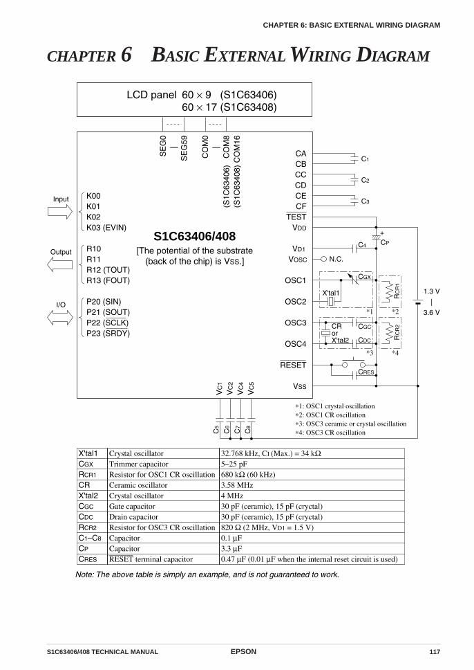
S1C63406/408 TECHNICAL MANUAL EPSON 117
CHAPTER 6: BASIC EXTERNAL WIRING DIAGRAM
CHAPTER 6 BASIC EXTERNAL WIRING DIAGRAM
CACBCCCDCECF
V
V
DD
D1
OSC1
OSC2
OSC3
OSC4
RESET
VSS
C1
C2
C3
C4
CGX
CDC
CRES
CP
1.3 V
|
3.6 V
+
X'tal1
N.C.
CRorX'tal2
*3 *4
RC
R2
*1 *2
RC
R1
K00K01K02K03 (EVIN)
R10R11R12 (TOUT)R13 (FOUT)
P20 (SIN)P21 (SOUT)P22 (SCLK)P23 (SRDY)
C5
C6
C7
C8
∗1: OSC1 crystal oscillation∗2: OSC1 CR oscillation∗3: OSC3 ceramic or crystal oscillation∗4: OSC3 CR oscillation
CGC
VOSC
TESTV V V V
C1
C2
C4
C5
I/O
Output
Input
X'tal1CGX
RCR1
CRX'tal2CGC
CDC
RCR2
C1–C8
CP
CRES
Crystal oscillatorTrimmer capacitorResistor for OSC1 CR oscillationCeramic oscillatorCrystal oscillatorGate capacitorDrain capacitorResistor for OSC3 CR oscillationCapacitorCapacitorRESET terminal capacitor
32.768 kHz, CI (Max.) = 34 kΩ5–25 pF680 kΩ (60 kHz)3.58 MHz4 MHz30 pF (ceramic), 15 pF (cryctal)30 pF (ceramic), 15 pF (cryctal)820 Ω (2 MHz, VD1 = 1.5 V)0.1 µF3.3 µF0.47 µF (0.01 µF when the internal reset circuit is used)
Note: The above table is simply an example, and is not guaranteed to work.
S1C63406/408[The potential of the substrate
(back of the chip) is VSS.]
SE
G0
|
SE
G59
CO
M0
|
(S1C
6340
6)
CO
M8
(S1C
6340
8) C
OM
16
LCD panel 60 × 9 (S1C63406)60 × 17 (S1C63408)
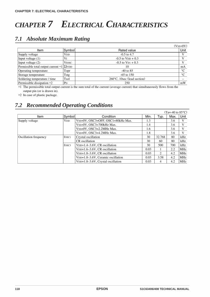
118 EPSON S1C63406/408 TECHNICAL MANUAL
CHAPTER 7: ELECTRICAL CHARACTERISTICS
CHAPTER 7 ELECTRICAL CHARACTERISTICS
7.1 Absolute Maximum Rating
ItemSupply voltageInput voltage (1)Input voltage (2)Permissible total output current ∗1Operating temperatureStorage temperatureSoldering temperature / timePermissible dissipation ∗2∗1
∗2
(VSS=0V)
SymbolVDD
VI
VIOSC
ΣIVDD
ToprTstgTsolPD
Rated value-0.5 to 4.7
-0.5 to VDD + 0.3-0.5 to VD1 + 0.3
10-40 to 85-65 to 150
260°C, 10sec (lead section)250
UnitVVV
mA°C°C–
mWThe permissible total output current is the sum total of the current (average current) that simultaneously flows from the output pin (or is drawn in).In case of plastic package.
7.2 Recommended Operating Conditions
ItemSupply voltage
Oscillation frequency
(Ta=-40 to 85°C)
SymbolVDD
fOSC1
fOSC3
UnitVVVV
kHzkHzkHzMHzMHzMHzMHz
Max.3.63.63.63.680807002.24.24.24.2
Typ.
32.7686050012
3.584
Min.1.31.41.61.8303030
0.030.030.030.03
ConditionVSS=0V, OSC3=OFF, OSC1=80kHz Max.VSS=0V, OSC3=700kHz Max.VSS=0V, OSC3=2.2MHz Max.VSS=0V, OSC3=4.2MHz Max.Crystal oscillationCR oscillationVDD=1.4–3.6V, CR oscillationVDD=1.6–3.6V, CR oscillationVDD=1.8–3.6V, CR oscillationVDD=1.8–3.6V, Ceramic oscillationVDD=1.8–3.6V, Crystal oscillation
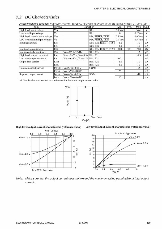
S1C63406/408 TECHNICAL MANUAL EPSON 119
CHAPTER 7: ELECTRICAL CHARACTERISTICS
7.3 DC Characteristics
ItemHigh level input voltageLow level input voltageHigh level schmitt input voltageLow level schmitt input voltageInput leak current
Input pull-up resistanceInput terminal capacitanceHigh level output current ∗1Low level output current ∗1Output leak current
Common output current
Segment output current
∗1
Unless otherwise specified: VDD=3.6V, VSS=0V, Ta=25°C, VD1/VOSC/VC1/VC2/VC4/VC5 are internal voltage, C1–C8=0.1µFSymbolVIH
VIL
VT+
VT-
ILIH
ILIL
RIN
CIN
IOH
IOL
ILOH
ILOL
ICOMH
ICOML
ISEGH
ISEGL
UnitVVVV
µAµAkΩpFmAmAµAµAµAµAµAµA
Max.VDD
0.2·VDD
0.9·VDD
0.5·VDD
1.01.050015
-0.3
1.01.0-25
-10
Typ.
300
Min.0.8·VDD
00.5·VDD
0.1·VDD
-1.0-1.0100
0.3-1.0-1.0
25
10See the characteristic curve as reference for the actual output current value.
ConditionK0xK0xP2x, RESET, TESTP2x, RESET, TESTK0x, P2x, RESET, TESTK0x, P2xK0x, P2x, RESET, TEST
VIN=0V, f=32kHz K0x, P2xVOH1=0.9·VDD, VDD=1.3V R1x, P2xVOL1=0.1·VDD, VDD=1.3V R1x, P2x
R1x, P2xR1x, P2x
VOH2=VC5-0.05V COMxVOL2=VSS+0.05VVOH3=VC5-0.05V SEGxxVOL3=VSS+0.05V
VDD
VDDVT+
VIN [V]
VO
UT [V
]
VT-0
0
-2
-4
-6
-8
-10
-12
20
18
16
14
12
10
8
6
4
2
0
0.0
0.0 0.2 0.4 0.6 0.8 1.0
0.20.4
VDD - VOH [V]
VOL [V]
IOH [m
A]
IOL
[mA
]
0.60.81.0
VDD = 1.3 V
VDD = 2.5 V
VDD = 3.6 VVDD = 1.3 V
VDD = 2.5 V
VDD = 3.6 V
Ta = 25°C, Typ. value
Ta = 25°C, Typ. value
High-level output current characteristic (reference value) Low-level output current characteristic (reference value)
Note: Make sure that the output current does not exceed the maximum rating permissible of total outputcurrent.

120 EPSON S1C63406/408 TECHNICAL MANUAL
CHAPTER 7: ELECTRICAL CHARACTERISTICS
7.4 Analog Circuit Characteristics and Power Current Consumption
LCD driver
ItemLCD drive voltage(when VC1 standard is selected)
LCD drive voltage(when VC2 standard is selected)
SymbolVC1
VC2
VC4
VC5
VC1
VC2
VC4
VC5
UnitV
V
V
V
V
V
V
V
Max.
Typ.×1.12
2·VC1
3·VC1
4·VC1
1/2·VC2
+0.1
Typ.×1.12
3/2·VC2
2·VC2
Typ.0.980.991.011.021.041.051.071.081.101.111.131.141.161.171.191.20
1.951.982.012.042.072.102.132.162.192.222.252.282.312.342.372.40
Min.
Typ.×0.88
2·VC1
×0.93·VC1
×0.94·VC1
×0.91/2·VC2
×0.95
Typ.×0.88
3/2·VC2
×0.952·VC2
×0.95
ConditionConnect 1 MΩ load resistor LC0–3="0"between VSS and VC1 LC0–3="1"(without panel load) LC0–3="2"
LC0–3="3"LC0–3="4"LC0–3="5"LC0–3="6"LC0–3="7"LC0–3="8"LC0–3="9"LC0–3="10"LC0–3="11"LC0–3="12"LC0–3="13"LC0–3="14"LC0–3="15"
Connect 1 MΩ load resistor between VSS and VC2
(without panel load)Connect 1 MΩ load resistor between VSS and VC4
(without panel load)Connect 1 MΩ load resistor between VSS and VC5
(without panel load)Connect 1 MΩ load resistor between VSS and VC1
(without panel load)Connect 1 MΩ load resistor LC0–3="0"between VSS and VC2 LC0–3="1"(without panel load) LC0–3="2"
LC0–3="3"LC0–3="4"LC0–3="5"LC0–3="6"LC0–3="7"LC0–3="8"LC0–3="9"LC0–3="10"LC0–3="11"LC0–3="12"LC0–3="13"LC0–3="14"LC0–3="15"
Connect 1 MΩ load resistor between VSS and VC4
(without panel load)Connect 1 MΩ load resistor between VSS and VC5
(without panel load)
Unless otherwise specified: VDD=3.6V, VSS=0V, fOSC1=32.768kHz, CG=5pF, Ta=25°C, VD1/VOSC/VC1/VC2/VC4/VC5 are internal voltage, C1–C8=0.1µF
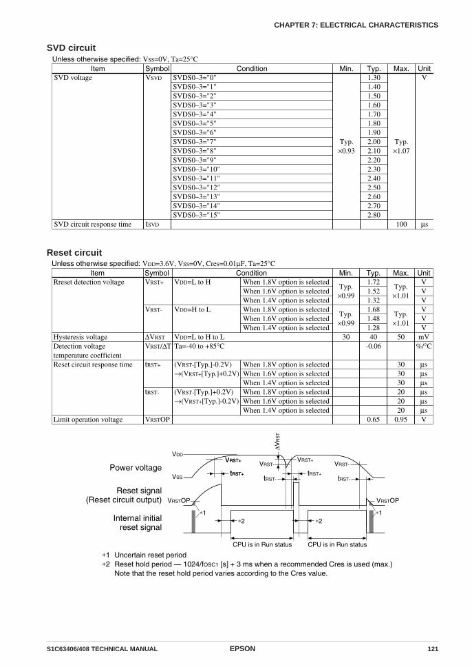
S1C63406/408 TECHNICAL MANUAL EPSON 121
CHAPTER 7: ELECTRICAL CHARACTERISTICS
SVD circuit
Item Symbol UnitMax.Typ.Min.ConditionUnless otherwise specified: VSS=0V, Ta=25°C
SVD voltage
SVD circuit response time
VSVD
tSVD
V
µs
Typ.×1.07
100
1.301.401.501.601.701.801.902.002.102.202.302.402.502.602.702.80
Typ.×0.93
SVDS0–3="0"SVDS0–3="1"SVDS0–3="2"SVDS0–3="3"SVDS0–3="4"SVDS0–3="5"SVDS0–3="6"SVDS0–3="7"SVDS0–3="8"SVDS0–3="9"SVDS0–3="10"SVDS0–3="11"SVDS0–3="12"SVDS0–3="13"SVDS0–3="14"SVDS0–3="15"
Reset circuit
Item Symbol UnitMax.Typ.Min.ConditionUnless otherwise specified: VDD=3.6V, VSS=0V, Cres=0.01µF, Ta=25°C
Rreset detection voltage
Hysteresis voltageDetection voltage temperature coefficientReset circuit response time
Limit operation voltage
VRST+
VRST-
∆VRST
VRST/∆T
tRST+
tRST-
VRSTOP
VVVVVV
mV%/°C
µsµsµsµsµsµsV
Typ.×1.01
Typ.×1.01
50
303030202020
0.95
1.721.521.321.681.481.2840
-0.06
0.65
Typ.×0.99
Typ.×0.99
30
VDD=L to H When 1.8V option is selectedWhen 1.6V option is selectedWhen 1.4V option is selected
VDD=H to L When 1.8V option is selectedWhen 1.6V option is selectedWhen 1.4V option is selected
VDD=L to H to LTa=-40 to +85°C
(VRST-[Typ.]-0.2V) When 1.8V option is selected→(VRST+[Typ.]+0.2V) When 1.6V option is selected
When 1.4V option is selected(VRST-[Typ.]+0.2V) When 1.8V option is selected→(VRST+[Typ.]-0.2V) When 1.6V option is selected
When 1.4V option is selected
CPU is in Run status CPU is in Run status
VRST+ VRST+
tRST+tRST+
∗2 ∗2∗1
tRST- tRST-
∆VR
ST
VRST-VRST-
VDD
∗1
VRSTOP VRSTOP
VSS
∗1 Uncertain reset period∗2 Reset hold period — 1024/fOSC1 [s] + 3 ms when a recommended Cres is used (max.)
Note that the reset hold period varies according to the Cres value.
Power voltage
Reset signal(Reset circuit output)
Internal initialreset signal
VRST+
tRST+
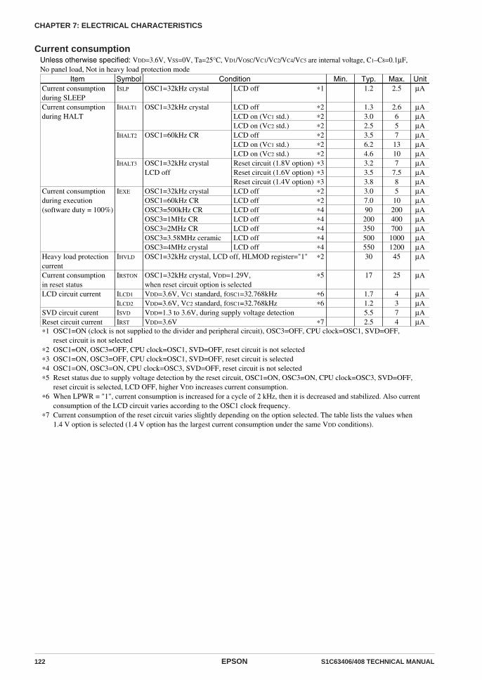
122 EPSON S1C63406/408 TECHNICAL MANUAL
CHAPTER 7: ELECTRICAL CHARACTERISTICS
Current consumption
ItemCurrent consumptionduring SLEEPCurrent consumptionduring HALT
Current consumptionduring execution(software duty = 100%)
Heavy load protection currentCurrent consumptionin reset statusLCD circuit current
SVD circuit curentReset circuit current∗1
∗2∗3∗4∗5
∗6
∗7
SymbolISLP
IHALT1
IHALT2
IHALT3
IEXE
IHVLD
IRSTON
ILCD1
ILCD2
ISVD
IRST
UnitµA
µAµAµAµAµAµAµAµAµAµAµAµAµAµAµAµAµA
µA
µAµAµAµA
Max.2.5
2.665713107
7.585102004007001000120045
25
4374
Typ.1.2
1.33.02.53.56.24.63.23.53.83.07.09020035050055030
17
1.71.25.52.5
Min.
OSC1=ON (clock is not supplied to the divider and peripheral circuit), OSC3=OFF, CPU clock=OSC1, SVD=OFF, reset circuit is not selectedOSC1=ON, OSC3=OFF, CPU clock=OSC1, SVD=OFF, reset circuit is not selectedOSC1=ON, OSC3=OFF, CPU clock=OSC1, SVD=OFF, reset circuit is selectedOSC1=ON, OSC3=ON, CPU clock=OSC3, SVD=OFF, reset circuit is not selectedReset status due to supply voltage detection by the reset circuit, OSC1=ON, OSC3=ON, CPU clock=OSC3, SVD=OFF, reset circuit is selected, LCD OFF, higher VDD increases current consumption.When LPWR = "1", current consumption is increased for a cycle of 2 kHz, then it is decreased and stabilized. Also current consumption of the LCD circuit varies according to the OSC1 clock frequency.Current consumption of the reset circuit varies slightly depending on the option selected. The table lists the values when 1.4 V option is selected (1.4 V option has the largest current consumption under the same VDD conditions).
ConditionOSC1=32kHz crystal LCD off ∗1
OSC1=32kHz crystal LCD off ∗2LCD on (VC1 std.) ∗2LCD on (VC2 std.) ∗2
OSC1=60kHz CR LCD off ∗2LCD on (VC1 std.) ∗2LCD on (VC2 std.) ∗2
OSC1=32kHz crystal Reset circuit (1.8V option) ∗3LCD off Reset circuit (1.6V option) ∗3
Reset circuit (1.4V option) ∗3OSC1=32kHz crystal LCD off ∗2OSC1=60kHz CR LCD off ∗2OSC3=500kHz CR LCD off ∗4OSC3=1MHz CR LCD off ∗4OSC3=2MHz CR LCD off ∗4OSC3=3.58MHz ceramic LCD off ∗4OSC3=4MHz crystal LCD off ∗4OSC1=32kHz crystal, LCD off, HLMOD register="1" ∗2
OSC1=32kHz crystal, VDD=1.29V, ∗5when reset circuit option is selectedVDD=3.6V, VC1 standard, fOSC1=32.768kHz ∗6VDD=3.6V, VC2 standard, fOSC1=32.768kHz ∗6VDD=1.3 to 3.6V, during supply voltage detectionVDD=3.6V ∗7
Unless otherwise specified: VDD=3.6V, VSS=0V, Ta=25°C, VD1/VOSC/VC1/VC2/VC4/VC5 are internal voltage, C1–C8=0.1µF, No panel load, Not in heavy load protection mode

S1C63406/408 TECHNICAL MANUAL EPSON 123
CHAPTER 7: ELECTRICAL CHARACTERISTICS
7.5 Oscillation CharacteristicsThe oscillation characteristics change depending on the conditions (components used, board pattern,etc.). Use the following characteristics as reference values.
OSC1 crystal oscillation circuit
ItemOscillation start timeBuilt-in capacitance (drain)Frequency/voltage deviationFrequency/IC deviationFrequency adjustment rangeHarmonic oscillation start voltagePermitted leak resistance
SymboltstaCD
∆f/∆V∆f/∆IC∆f/∆CG
Vhho
Rleak
Units
pFppmppmppm
VMΩ
Max.3
510
Typ.
14
20
Min.
-10103.6200
Condition
Including the parasitic capacitance inside the IC (in chip)VDD=1.3 to 3.6V
CG=5 to 25pFCG=5pF (VDD)Between OSC1 and VSS
Unless otherwise specified: VDD=1.3 to 3.6V, VSS=0V, fOSC1=32.768kHz, CG=25pF, CD=built-in, Ta=-40 to 85°C
OSC1 CR oscillation circuit
ItemOscillation frequency dispersionOscillation start time
SymbolfOSC1
tsta
Unit%µs
Max.25100
Typ.Min.-25
ConditionRCR1=constant
Unless otherwise specified: VDD=1.3 to 3.6V, VSS=0V, RCR1=680kΩ, Ta=-40 to 85°C
OSC3 ceramic oscillation circuit
ItemOscillation start time
Symboltsta
Unitms
Max.5
Typ.Min.ConditionUnless otherwise specified: VDD=1.8 to 3.6V, VSS=0V, Ceramic oscillator: 3.58MHz, CGC=CDC=30pF, Ta=-40 to 85°C
OSC3 crystal oscillation circuit
ItemOscillation start time
Symboltsta
Unitms
Max.10
Typ.Min.ConditionUnless otherwise specified: VDD=1.8 to 3.6V, VSS=0V, Crystal oscillator: 4MHz, CGC=CDC=15pF, Ta=-40 to 85°C
OSC3 CR oscillation circuit
ItemOscillation frequency dispersion
Oscillation start time
SymbolfOSC3
tsta
Unit%%%µs
Max.252525100
Typ.Min.-25-25-25
ConditionVDD=1.8 to 3.6V (VDC=3), RCR2=constantVDD=1.6 to 3.6V (VDC=2), RCR2=constantVDD=1.4 to 3.6V (VDC=1), RCR2=constant
Unless otherwise specified: VDD=1.4 to 3.6V, VSS=0V, RCR2=100kΩ, Ta=-40 to 85°C
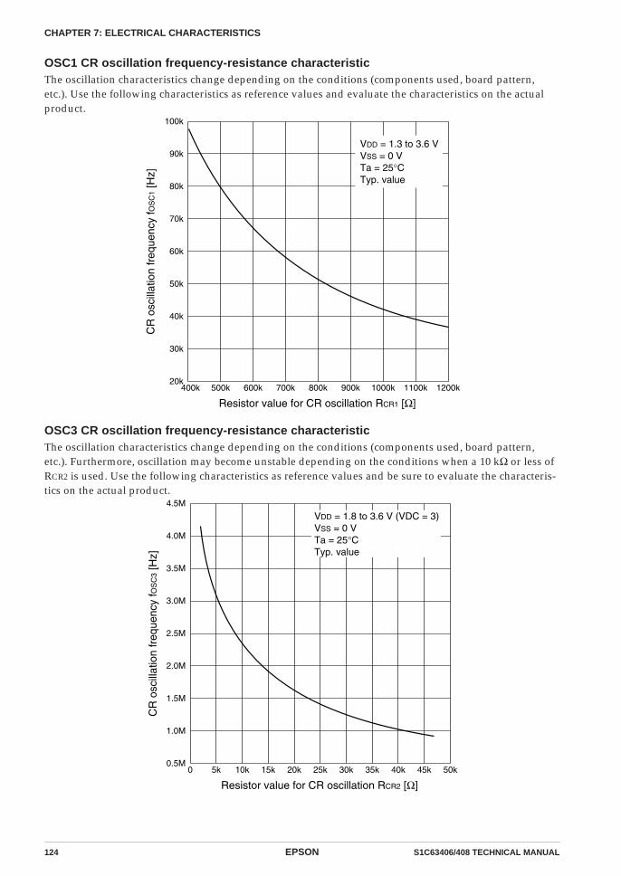
124 EPSON S1C63406/408 TECHNICAL MANUAL
CHAPTER 7: ELECTRICAL CHARACTERISTICS
OSC1 CR oscillation frequency-resistance characteristicThe oscillation characteristics change depending on the conditions (components used, board pattern,etc.). Use the following characteristics as reference values and evaluate the characteristics on the actualproduct.
Resistor value for CR oscillation RCR1 [Ω]
CR
osc
illat
ion
freq
uenc
y fO
SC
1 [H
z]VDD = 1.3 to 3.6 VVSS = 0 VTa = 25°CTyp. value
100k
90k
80k
70k
60k
50k
40k
30k
20k400k 500k 600k 700k 800k 900k 1000k 1100k 1200k
OSC3 CR oscillation frequency-resistance characteristicThe oscillation characteristics change depending on the conditions (components used, board pattern,etc.). Furthermore, oscillation may become unstable depending on the conditions when a 10 kΩ or less ofRCR2 is used. Use the following characteristics as reference values and be sure to evaluate the characteris-tics on the actual product.
Resistor value for CR oscillation RCR2 [Ω]
CR
osc
illat
ion
freq
uenc
y fO
SC
3 [H
z]
4.5M
4.0M
3.5M
3.0M
2.5M
2.0M
1.5M
1.0M
0.5M0 5k 10k 15k 20k 25k 30k 35k 40k 50k45k
VDD = 1.8 to 3.6 V (VDC = 3)VSS = 0 VTa = 25°CTyp. value
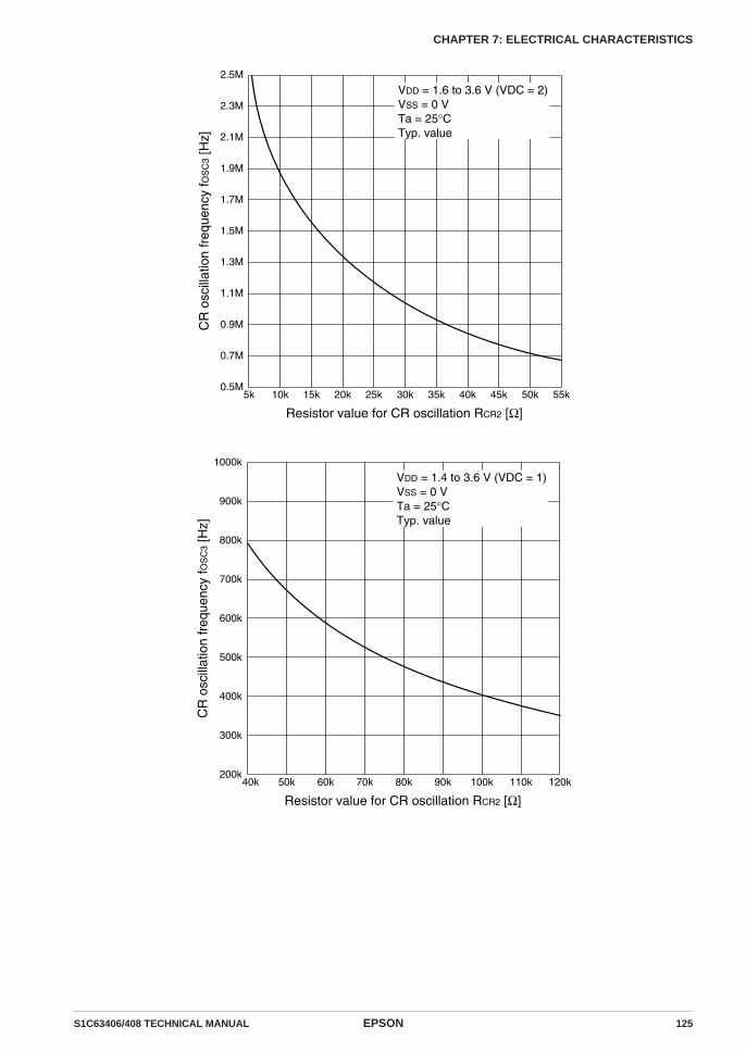
S1C63406/408 TECHNICAL MANUAL EPSON 125
CHAPTER 7: ELECTRICAL CHARACTERISTICS
Resistor value for CR oscillation RCR2 [Ω]
CR
osc
illat
ion
freq
uenc
y fO
SC
3 [H
z]
2.5M
2.3M
2.1M
1.9M
1.7M
1.5M
1.3M
1.1M
0.9M
0.7M
0.5M5k 55k10k 15k 20k 25k 30k 35k 40k 50k45k
VDD = 1.6 to 3.6 V (VDC = 2)VSS = 0 VTa = 25°CTyp. value
Resistor value for CR oscillation RCR2 [Ω]
CR
osc
illat
ion
freq
uenc
y fO
SC
3 [H
z]
1000k
900k
800k
700k
600k
500k
400k
300k
200k40k 50k 60k 70k 80k 90k 100k 110k 120k
VDD = 1.4 to 3.6 V (VDC = 1)VSS = 0 VTa = 25°CTyp. value
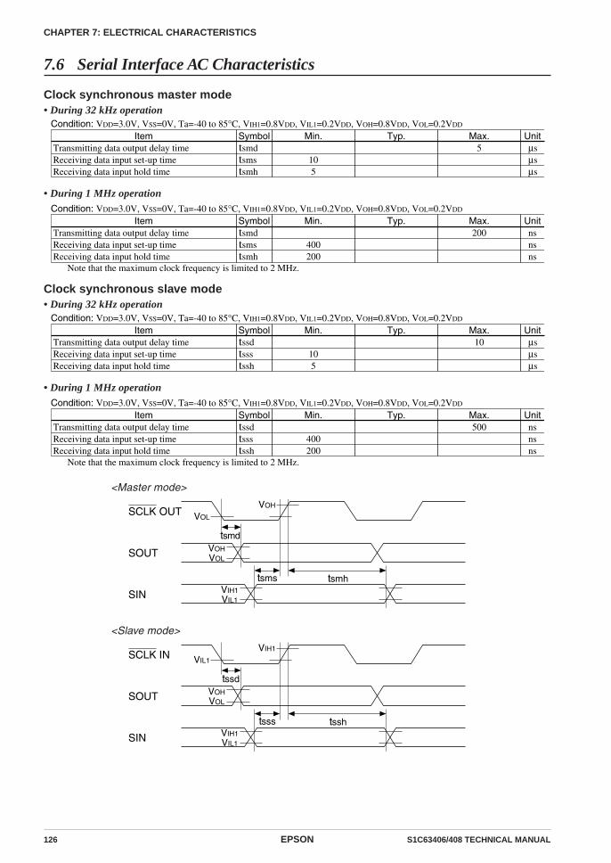
126 EPSON S1C63406/408 TECHNICAL MANUAL
CHAPTER 7: ELECTRICAL CHARACTERISTICS
7.6 Serial Interface AC Characteristics
Clock synchronous master mode• During 32 kHz operation
ItemTransmitting data output delay timeReceiving data input set-up timeReceiving data input hold time
Symboltsmdtsmstsmh
Unitµsµsµs
Max.5
Typ.Min.
105
Condition: VDD=3.0V, VSS=0V, Ta=-40 to 85°C, VIH1=0.8VDD, VIL1=0.2VDD, VOH=0.8VDD, VOL=0.2VDD
• During 1 MHz operation
ItemTransmitting data output delay timeReceiving data input set-up timeReceiving data input hold time
Symboltsmdtsmstsmh
Unitnsnsns
Max.200
Typ.Min.
400200
Note that the maximum clock frequency is limited to 2 MHz.
Condition: VDD=3.0V, VSS=0V, Ta=-40 to 85°C, VIH1=0.8VDD, VIL1=0.2VDD, VOH=0.8VDD, VOL=0.2VDD
Clock synchronous slave mode• During 32 kHz operation
ItemTransmitting data output delay timeReceiving data input set-up timeReceiving data input hold time
Symboltssdtssstssh
Unitµsµsµs
Max.10
Typ.Min.
105
Condition: VDD=3.0V, VSS=0V, Ta=-40 to 85°C, VIH1=0.8VDD, VIL1=0.2VDD, VOH=0.8VDD, VOL=0.2VDD
• During 1 MHz operation
ItemTransmitting data output delay timeReceiving data input set-up timeReceiving data input hold time
Symboltssdtssstssh
Unitnsnsns
Max.500
Typ.Min.
400200
Note that the maximum clock frequency is limited to 2 MHz.
Condition: VDD=3.0V, VSS=0V, Ta=-40 to 85°C, VIH1=0.8VDD, VIL1=0.2VDD, VOH=0.8VDD, VOL=0.2VDD
<Master mode>
SCLK OUT
SOUT
SIN
VOH
VOHVOL
tsms tsmh
tsmd
VIH1VIL1
VOL
<Slave mode>
SCLK IN
SOUT
SIN
VIH1
VOHVOL
tsss tssh
tssd
VIH1VIL1
VIL1

S1C63406/408 TECHNICAL MANUAL EPSON 127
CHAPTER 7: ELECTRICAL CHARACTERISTICS
Asynchronous system
ItemStart bit detection error time ∗1Erroneous start bit detection range time ∗2∗1
∗2
Symboltsa1
tsa2
Unitss
Max.t/16
10t/16
Typ.Min.0
9t/16Start bit detection error time is a logical delay time from inputting the start bit until internal sampling begins operating. (Time as far as AC is excluded.)Erroneous start bit detection range time is a logical range to detect whether a LOW level (start bit) has been input again after a start bit has been detected and the internal sampling clock has started. When a HIGH level is detected, the start bit detection circuit is reset and goes into a wait status until the next start bit. (Time as far as AC is excluded.)
Condition: VDD=1.4 to 3.6V, VSS=0V, Ta=-40 to 85°C
tsa1
t
tsa2
SIN
Start bit
Samplingclock
Erroneous start bit detection signal
Stop bit
7.7 Timing Chart
System clock switching
VDC1, 0
OSCC
CLKCHG
∗
∗
2.5 msec min.
5 msec min.
∗ 1 instruction execution time or longer
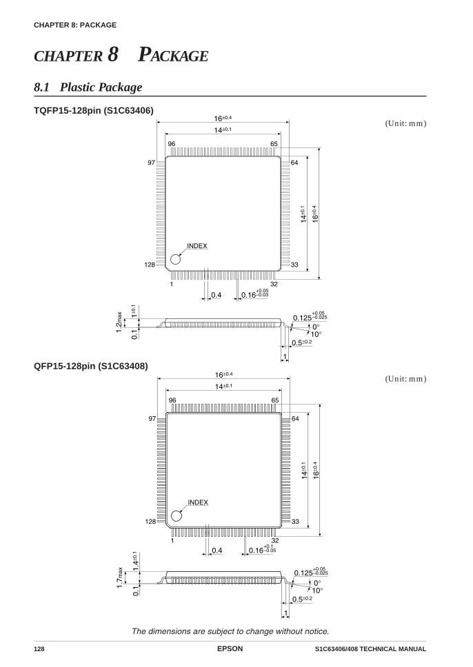
128 EPSON S1C63406/408 TECHNICAL MANUAL
CHAPTER 8: PACKAGE
CHAPTER 8 PACKAGE
8.1 Plastic Package
TQFP15-128pin (S1C63406)(Unit: mm)
QFP15-128pin (S1C63408)(Unit: mm)
6596
33
64
INDEX
321
128
97
14±0.1
16±0.4
14±0
.1
16±0
.4
0.160.4+0.05–0.03
1±0.
10.
11.2m
ax
1
0.5±0.2
0°10°
0.125+0.05–0.025
The dimensions are subject to change without notice.
14±0.1
16±0.4
6596
14±0
.1
16±0
.4
33
64
INDEX
0.16321
128
97
1.4±
0.1
0.11.
7max
1
0.5±0.2
0°10°
0.125
0.4+0.1–0.05
+0.05–0.025

S1C63406/408 TECHNICAL MANUAL EPSON 129
CHAPTER 8: PACKAGE
8.2 Ceramic Package for Test Samples
QFP8-128pin(Unit: mm)
28±0.28
32±0.4
28±0
.28
32±0
.4
0.8 0.35
0.23.
05m
ax
0.8±0.2
0.15
6596
33
64
321
128
97
INDEX

130 EPSON S1C63406/408 TECHNICAL MANUAL
CHAPTER 9: PAD LAYOUT
CHAPTER 9 PAD LAYOUT
9.1 Diagram of Pad Layout
Chip thickness: 400 µmPad opening: 100 µm
X
Y
(0, 0)
3.46 mm
3.62
mm
15101520
30
104
106
35
40
45
5080
85
90
95
100
10325
55 60 65 70 75
Die
No.
S1C63406
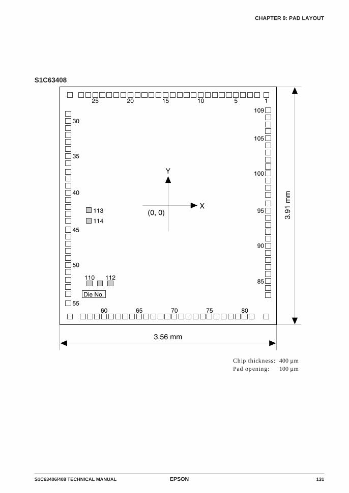
S1C63406/408 TECHNICAL MANUAL EPSON 131
CHAPTER 9: PAD LAYOUT
S1C63408
X
Y
(0, 0)
3.56 mm
3.91
mm
15101520
30
35
40
45
114
113
50
55
85
90
95
100
105
109
60 65 70 75 80
25
112110
Die No.
Chip thickness: 400 µmPad opening: 100 µm
132 EPSON S1C63406/408 TECHNICAL MANUAL
CHAPTER 9: PAD LAYOUT
No.
1
2
3
4
5
6
7
8
9
10
11
12
13
14
15
16
17
18
19
20
21
22
23
24
25
26
27
28
29
30
31
32
33
34
35
36
Pad name
CF
VC5
VC4
VC2
VC1
K00
K01
K02
K03
R10
R11
R12
R13
P20
P21
P22
P23
VDD
VD1
OSC4
OSC3
VOSC
OSC2
OSC1
VSS
RESET
TEST
N.C.
N.C.
COM0
COM1
COM2
COM3
COM4
COM5
COM6
X
1,536
1,394
1,279
1,163
1,048
932
817
701
586
470
355
239
124
8
-107
-223
-338
-454
-569
-685
-800
-916
-1,031
-1,147
-1,262
-1,390
-1,506
-1,595
-1,595
-1,595
-1,595
-1,595
-1,595
-1,595
-1,595
-1,595
Y
1,674
1,674
1,674
1,674
1,674
1,674
1,674
1,674
1,674
1,674
1,674
1,674
1,674
1,674
1,674
1,674
1,674
1,674
1,674
1,674
1,674
1,674
1,674
1,674
1,674
1,674
1,674
1,278
1,107
967
851
736
620
505
389
274
No.
37
38
39
40
41
42
43
44
45
46
47
48
49
50
51
52
53
54
55
56
57
58
59
60
61
62
63
64
65
66
67
68
69
70
71
72
Pad name
COM7
SEG0
SEG1
SEG2
SEG3
SEG4
SEG5
SEG6
SEG7
SEG8
SEG9
SEG10
SEG11
SEG12
SEG13
SEG14
SEG15
SEG16
SEG17
SEG18
SEG19
SEG20
SEG21
SEG22
SEG23
SEG24
SEG25
SEG26
SEG27
SEG28
SEG29
SEG30
SEG31
SEG32
SEG33
SEG34
X
-1,595
-1,595
-1,595
-1,595
-1,595
-1,595
-1,595
-1,595
-1,595
-1,595
-1,595
-1,595
-1,595
-1,595
-1,595
-1,595
-1,378
-1,262
-1,147
-1,031
-916
-800
-685
-569
-454
-338
-223
-107
8
124
239
355
470
586
701
817
Y
158
28
-88
-203
-319
-434
-550
-665
-781
-896
-1,012
-1,127
-1,243
-1,358
-1,474
-1,616
-1,674
-1,674
-1,674
-1,674
-1,674
-1,674
-1,674
-1,674
-1,674
-1,674
-1,674
-1,674
-1,674
-1,674
-1,674
-1,674
-1,674
-1,674
-1,674
-1,674
No.
73
74
75
76
77
78
79
80
81
82
83
84
85
86
87
88
89
90
91
92
93
94
95
96
97
98
99
100
101
102
103
104
105
106
–
–
Pad name
SEG35
SEG36
SEG37
SEG38
SEG39
SEG40
SEG41
SEG42
SEG43
SEG44
SEG45
SEG46
SEG47
SEG48
SEG49
SEG50
SEG51
SEG52
SEG53
SEG54
SEG55
SEG56
SEG57
SEG58
SEG59
COM8
CA
CB
CC
CD
CE
N.C.
N.C.
N.C.
X
932
1,048
1,163
1,279
1,394
1,563
1,595
1,595
1,595
1,595
1,595
1,595
1,595
1,595
1,595
1,595
1,595
1,595
1,595
1,595
1,595
1,595
1,595
1,595
1,595
1,595
1,595
1,595
1,595
1,595
1,595
-1,256
-1,256
-1,256
Y
-1,674
-1,674
-1,674
-1,674
-1,674
-1,674
-1,340
-1,224
-1,109
-993
-878
-762
-647
-531
-416
-300
-185
-69
46
162
277
393
508
624
739
870
985
1,101
1,216
1,332
1,447
1,448
1,277
1,106
Unit: µm
9.2 Pad Coordinates
S1C63406

S1C63406/408 TECHNICAL MANUAL EPSON 133
CHAPTER 9: PAD LAYOUT
S1C63408No.
1
2
3
4
5
6
7
8
9
10
11
12
13
14
15
16
17
18
19
20
21
22
23
24
25
26
27
28
29
30
31
32
33
34
35
36
37
38
Pad name
CE
CF
VC5
VC4
VC2
VC1
K00
K01
K02
K03
R10
R11
R12
R13
P20
P21
P22
P23
VDD
VD1
OSC4
OSC3
VOSC
OSC2
OSC1
VSS
RESET
TEST
COM0
COM1
COM2
COM3
COM4
COM5
COM6
COM7
SEG0
SEG1
X
1,611
1,460
1,344
1,229
1,113
998
882
767
651
536
420
305
189
74
-42
-158
-273
-389
-504
-620
-735
-851
-966
-1,082
-1,197
-1,313
-1,428
-1,610
-1,642
-1,642
-1,642
-1,642
-1,642
-1,642
-1,642
-1,642
-1,642
-1,642
Y
1,818
1,818
1,818
1,818
1,818
1,818
1,818
1,818
1,818
1,818
1,818
1,818
1,818
1,818
1,818
1,818
1,818
1,818
1,818
1,818
1,818
1,818
1,818
1,818
1,818
1,818
1,818
1,818
1,508
1,393
1,277
1,162
1,046
931
815
700
559
444
No.
39
40
41
42
43
44
45
46
47
48
49
50
51
52
53
54
55
56
57
58
59
60
61
62
63
64
65
66
67
68
69
70
71
72
73
74
75
76
Pad name
SEG2
SEG3
SEG4
SEG5
SEG6
SEG7
SEG8
SEG9
SEG10
SEG11
SEG12
SEG13
SEG14
SEG15
SEG16
SEG17
SEG18
SEG19
SEG20
SEG21
SEG22
SEG23
SEG24
SEG25
SEG26
SEG27
SEG28
SEG29
SEG30
SEG31
SEG32
SEG33
SEG34
SEG35
SEG36
SEG37
SEG38
SEG39
X
-1,642
-1,642
-1,642
-1,642
-1,642
-1,642
-1,642
-1,642
-1,642
-1,642
-1,642
-1,642
-1,642
-1,642
-1,642
-1,642
-1,642
-1,610
-1,399
-1,283
-1,168
-1,052
-937
-821
-706
-590
-475
-359
-244
-128
-13
103
218
334
449
565
680
796
Y
328
213
97
-19
-134
-250
-393
-509
-624
-740
-855
-971
-1,086
-1,215
-1,331
-1,446
-1,601
-1,818
-1,818
-1,818
-1,818
-1,818
-1,818
-1,818
-1,818
-1,818
-1,818
-1,818
-1,818
-1,818
-1,818
-1,818
-1,818
-1,818
-1,818
-1,818
-1,818
-1,818
No.
77
78
79
80
81
82
83
84
85
86
87
88
89
90
91
92
93
94
95
96
97
98
99
100
101
102
103
104
105
106
107
108
109
110
111
112
113
114
Pad name
SEG40
SEG41
SEG42
SEG43
SEG44
SEG45
SEG46
SEG47
SEG48
SEG49
SEG50
SEG51
SEG52
SEG53
SEG54
SEG55
SEG56
SEG57
SEG58
SEG59
COM8
COM9
COM10
COM11
COM12
COM13
COM14
COM15
COM16
CA
CB
CC
CD
N.C.
N.C.
N.C.
N.C.
N.C.
X
911
1,027
1,142
1,258
1,373
1,612
1,642
1,642
1,642
1,642
1,642
1,642
1,642
1,642
1,642
1,642
1,642
1,642
1,642
1,642
1,642
1,642
1,642
1,642
1,642
1,642
1,642
1,642
1,642
1,642
1,642
1,642
1,642
-1,290
-1,119
-948
-1,301
-1,301
Y
-1,818
-1,818
-1,818
-1,818
-1,818
-1,818
-1,466
-1,350
-1,235
-1,119
-1,004
-888
-773
-657
-542
-426
-311
-195
-80
36
181
297
412
528
643
759
874
990
1,105
1,221
1,336
1,452
1,567
-1,273
-1,273
-1,273
-73
-244
Unit: µm
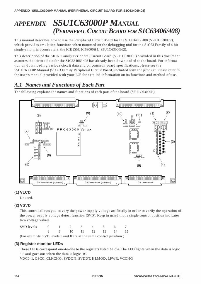
134 EPSON S1C63406/408 TECHNICAL MANUAL
APPENDIX S5U1C63000P MANUAL (PERIPHERAL CIRCUIT BOARD FOR S1C63406/408)
APPENDIX S5U1C63000P MANUAL(PERIPHERAL CIRCUIT BOARD FOR S1C63406/408)
This manual describes how to use the Peripheral Circuit Board for the S1C63406/408 (S5U1C63000P),which provides emulation functions when mounted on the debugging tool for the S1C63 Family of 4-bitsingle-chip microcomputers, the ICE (S5U1C63000H1/S5U1C63000H2).
This description of the S1C63 Family Peripheral Circuit Board (S5U1C63000P) provided in this documentassumes that circuit data for the S1C63406/408 has already been downloaded to the board. For informa-tion on downloading various circuit data and on common board specifications, please see theS5U1C63000P Manual (S1C63 Family Peripheral Circuit Board) included with the product. Please refer tothe user’s manual provided with your ICE for detailed information on its functions and method of use.
A.1 Names and Functions of Each PartThe following explains the names and functions of each part of the board (S5U1C63000P).
V S V DF
PG
A
Prog PRG Norm
1 12
15
LEDVC5
V L C D
P R C 6 3 0 0 0 Ver. x.x
VC5CLKCN0 GND
GND FOSC3(CR)
FOSC1(CR)ADOSCA
REST
SN0 ST1 ST0
LCLK32K
EPR
OM
CO
NFI
G S
ELFl
ash
CPA
1
EIOSE
L2
OSC1
(CR)
Adj
OSC3
(CR)
Adj
D
CN3 connector (not used) CN2 connector (not used) CN1 connector
16 16
(3)
(4)(9)
(1) (2)(11)(10)(9)
(8)
(7)
(6)
(5)
(1) VLCDUnused.
(2) VSVDThis control allows you to vary the power supply voltage artificially in order to verify the operation ofthe power supply voltage detect function (SVD). Keep in mind that a single control position indicatestwo voltage values.
SVD levels 0 1 2 3 4 5 6 78 9 10 11 12 13 14 15
(For example, SVD levels 0 and 8 are at the same control position.)
(3) Register monitor LEDsThese LEDs correspond one-to-one to the registers listed below. The LED lights when the data is logic"1" and goes out when the data is logic "0".VDC0–1, OSCC, CLKCHG, SVDON, SVDDT, HLMOD, LPWR, VCCHG

S1C63406/408 TECHNICAL MANUAL EPSON 135
APPENDIX S5U1C63000P MANUAL (PERIPHERAL CIRCUIT BOARD FOR S1C63406/408)
(4) Register monitor pinsThese pins correspond one-to-one to the registers listed below. The pin outputs a high for logic "1"and a low for logic "0".
Pin No.
1
2
3
4
5
6
7
8
9
10
11
12
13
14
15
16
Monitor
∗ DONE: The monitor pin outputs a high while the LED lights wheninitialization of this board completes without problems.
Name
DONE *
VDC0
VDC1
OSCC
CLKCHG
SVDON
SVDDT
HLMOD
LPWR
VCCHG
–
–
–
–
–
–
LED No.
1
2
3
4
5
6
7
8
9
10
11
12
13
14
15
16
LED
Name
DONE *
VDC0
VDC1
OSCC
CLKCHG
SVDON
SVDDT
HLMOD
LPWR
VCCHG
–
–
–
–
–
–Monitor pin
12345678910111213141516
1
3
5
7
9
11
13
15
2
4
6
8
10
12
14
16
LED
(5) CR oscillation frequency adjusting controlWhen OSC1 and/or OSC3 are set for a CR oscillation circuit by a mask option, this control allows youto adjust the oscillation frequency. The oscillation frequency can be adjusted in the range of approx. 20kHz to 500 kHz for OSC1 and approx. 100 kHz to 8 MHz for OSC3. Note that the actual IC does notoperate with all of these frequencies; refer to Section 4.3, "Oscillation Circuit", to select the appropriateoperating frequency.
OSC1 rough adjustment
OSC1 fine adjustment
OSC3 rough adjustment
OSC3 fine adjustment
(6) CR oscillation frequency monitor pinsThese pins allow you to monitor the clock waveform from the CR oscillation circuit with an oscillo-scope. Note that these pins always output a signal waveform whether or not the oscillation circuit isoperating.
OSC3 monitor pin (red)
OSC1 monitor pin (red)
GND pin (black)
RESET
(7) RESET switchThis switch initializes the internal circuits of this board and feeds a reset signal to the ICE.

136 EPSON S1C63406/408 TECHNICAL MANUAL
APPENDIX S5U1C63000P MANUAL (PERIPHERAL CIRCUIT BOARD FOR S1C63406/408)
(8) Monitor pins and external part connecting socketThese parts are currently unused.
(9) CLK and PRG switchIf power to the ICE is shut down before circuit data downloading is complete, the circuit configura-tion in this board will remain incomplete, and the debugger may not be able to start when you poweron the ICE once again. In this case, temporarily power off the ICE and set CLK to the 32K position andthe PRG switch to the Prog position, then switch on power for the ICE once again. This should allowthe debugger to start up, allowing you to download circuit data. After downloading the circuit data,temporarily power off the ICE and reset CLK and PRG to the LCLK and the Norm position, respec-tively. Then power on the ICE once again.
(10) IOSEL2When downloading circuit data, set IOSEL2 to the "E" position. Otherwise, set to the "D" position.
(11) VC5This control allows fine adjustment of the LCD drive voltage. Note, however, that only the LCDcontrast register can adjust the LCD drive voltage in the actual IC.
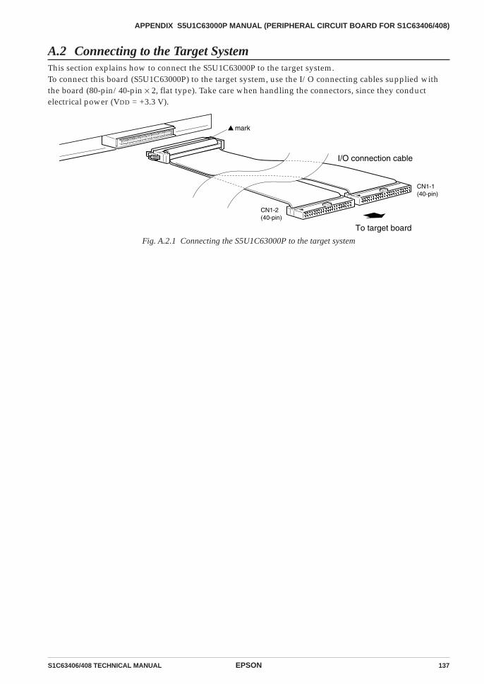
S1C63406/408 TECHNICAL MANUAL EPSON 137
APPENDIX S5U1C63000P MANUAL (PERIPHERAL CIRCUIT BOARD FOR S1C63406/408)
A.2 Connecting to the Target SystemThis section explains how to connect the S5U1C63000P to the target system.To connect this board (S5U1C63000P) to the target system, use the I/O connecting cables supplied withthe board (80-pin/40-pin × 2, flat type). Take care when handling the connectors, since they conductelectrical power (VDD = +3.3 V).
CN1-1(40-pin)
I/O connection cable
To target board
CN1-2(40-pin)
mark
Fig. A.2.1 Connecting the S5U1C63000P to the target system
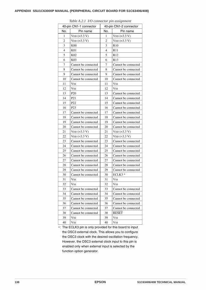
138 EPSON S1C63406/408 TECHNICAL MANUAL
APPENDIX S5U1C63000P MANUAL (PERIPHERAL CIRCUIT BOARD FOR S1C63406/408)
Table A.2.1 I/O connector pin assignment
No.
1
2
3
4
5
6
7
8
9
10
11
12
13
14
15
16
17
18
19
20
21
22
23
24
25
26
27
28
29
30
31
32
33
34
35
36
37
38
39
40
40-pin CN1-1 connector
Pin name
VDD (=3.3 V)
VDD (=3.3 V)
K00
K01
K02
K03
Cannot be connected
Cannot be connected
Cannot be connected
Cannot be connected
VSS
VSS
P20
P21
P22
P23
Cannot be connected
Cannot be connected
Cannot be connected
Cannot be connected
VDD (=3.3 V)
VDD (=3.3 V)
Cannot be connected
Cannot be connected
Cannot be connected
Cannot be connected
Cannot be connected
Cannot be connected
Cannot be connected
Cannot be connected
VSS
VSS
Cannot be connected
Cannot be connected
Cannot be connected
Cannot be connected
Cannot be connected
Cannot be connected
VSS
VSS
No.
1
2
3
4
5
6
7
8
9
10
11
12
13
14
15
16
17
18
19
20
21
22
23
24
25
26
27
28
29
30
31
32
33
34
35
36
37
38
39
40
40-pin CN1-2 connector
Pin name
VDD (=3.3 V)
VDD (=3.3 V)
R10
R11
R12
R13
Cannot be connected
Cannot be connected
Cannot be connected
Cannot be connected
VSS
VSS
Cannot be connected
Cannot be connected
Cannot be connected
Cannot be connected
Cannot be connected
Cannot be connected
Cannot be connected
Cannot be connected
VDD (=3.3 V)
VDD (=3.3 V)
Cannot be connected
Cannot be connected
Cannot be connected
Cannot be connected
Cannot be connected
Cannot be connected
Cannot be connected
ECLK3 *
VSS
VSS
Cannot be connected
Cannot be connected
Cannot be connected
Cannot be connected
Cannot be connected
RESET
VSS
VSS
∗: The ECLK3 pin is only provided for this board to input
the OSC3 external clock. This allows you to configure
the OSC3 clock with the desired oscillation frequency.
However, the OSC3 external clock input to this pin is
enabled only when external input is selected by the
function option generator.
S1C63406/408 TECHNICAL MANUAL EPSON 139
APPENDIX S5U1C63000P MANUAL (PERIPHERAL CIRCUIT BOARD FOR S1C63406/408)
A.3 Usage PrecautionsTo ensure correct use of this board (S5U1C63000P), please observe the following precautions.
A.3.1 Operational precautions(1) Before inserting or removing cables, turn off power to all pieces of connected equipment.
(2) Do not turn on power or load mask option data if all of the input ports (K00–K03) are held low. Doingso may activate the multiple key entry reset function.
(3) Before debugging, always be sure to load mask option data.
A.3.2 Differences with the actual IC(1) Differences in I/O
<Interface power supply>This board and target system interface voltage is set to +3.3 V. To obtain the same interface voltage asin the actual IC, attach a level shifter circuit, etc. on the target system side to accommodate therequired interface voltage.
<Each output port’s drive capability>The drive capability of each output port on this board is higher than that of the actual IC. Whendesigning application system and software, refer to Chapter 7, "Electrical Characteristics", to confirmeach output port’s drive capability.
<Each port’s protective diode>All I/O ports incorporate a protective diode for VDD and VSS, and the interface signals between thisboard and the target system are set to +3.3 V. Therefore, this board and the target system cannot beinterfaced with voltages exceeding VDD by setting the output ports for open-drain mode.
<Pull-up resistance value>The pull-up resistance values on this board are set to 220 kΩ which differ from those for the actual IC.For the resistance values on the actual IC, refer to Chapter 7, "Electrical Characteristics".Note that when using pull-up resistors to pull the input pins high, the input pins may require acertain period to reach a valid high level. Exercise caution if a key matrix circuit is configured using acombination of output and input ports, since rise delay times on these input ports differ from those ofthe actual IC.
(2) Differences in current consumptionThe amount of current consumed by this board differs significantly from that of the actual IC. Inspect-ing the LEDs on this board may help you keep track of approximate current consumption. Thefollowing factors/components greatly affect device current consumption:
<Those which can be verified by LEDs and monitor pins>a) Run and Halt execution ratio (verified by LEDs and monitor pins on the ICE)b) CPU operating voltage change (VDC0, VDC1)c) OSC3 oscillation on/off (OSCC)d) CPU clock change (CLKCHG)e) SVD circuit on/off (SVDON)f) Heavy load protection mode (HLMOD)g) LCD power supply on/off (LPWR)h) LCD constant-voltage change (VCCHG)
<Those that can only be counteracted by system or software>i) Current consumed by the internal pull-up resistorsj) Input ports in a floating state

140 EPSON S1C63406/408 TECHNICAL MANUAL
APPENDIX S5U1C63000P MANUAL (PERIPHERAL CIRCUIT BOARD FOR S1C63406/408)
(3) Functional precautions<LCD power supply circuit>There is a finite delay time from the point at which the LCD power supply circuit (LPWR) turns onuntil an LCD drive waveform is output. On this board, this delay is set to approx. 125 msec, whichdiffers from that of the actual IC.
<SVD circuit>- Although the S1C63406/408 has a function for detecting externally sourced voltages, this board is
unable to detect externally sourced voltages. The SVD function is realized by artificially varying thepower supply voltage using the VSVD control on this board.
- There is a finite delay time from when the power to the SVD circuit turns on until actual detection ofthe voltage. On this board, this delay is set to 61–92 µsec, which differs from that of the actual IC.Refer to Section 4.12, "SVD Circuit", when setting the appropriate wait time for the actual IC.
<Oscillation circuit>- A wait time is required before oscillation stabilizes after the OSC3 oscillation control circuit (OSCC)
is turned on. On this board, even when OSC3 oscillation is changed (CLKCHG) without a wait time,OSC3 will function normally. Refer to Section 4.3, "Oscillation Circuit", when setting the appropriatewait time for the actual IC.
- Use separate instructions to switch the clock from OSC3 to OSC1 and to turn off the OSC3 oscillationcircuit. If executed simultaneously with a single instruction, these operations, although good withthis board, may not function properly well with the actual IC.
- Because the logic level of the oscillation circuit is high, the timing at which the oscillation starts onthis board differs from that of the actual IC.
- This board contains oscillation circuits for OSC1 and OSC3. Keep in mind that even though theactual IC may not have a resonator connected to its OSC3, its emulator can operate with the OSC3circuit.
- It is necessary to select the appropriate operating voltage for the internal circuits before the OSC3oscillation circuit can be turned on in the actual IC. Be aware that this board can operate normallyeven if an illegal voltage is selected.
- When using an external clock for OSC3, adjust the amplitude of the clock to 3.3 V ± 5% and the dutyratio to 50% ± 10%, and input it to the ECLK3 pin with VSS as the ground.
<Access to undefined address space>If any undefined space in the S1C63406/408's internal ROM/RAM or I/O is accessed for data read orwrite operations, the read/written value is indeterminate. Additionally, it is important to remainaware that indeterminate state differs between this board and the actual IC. Note that the ICE(S5U1C63000H1/S5U1C63000H2) incorporates the program break function caused by accessing to anundefined address space.
<Reset circuit>Keep in mind that the operation sequence from when the ICE and this board are powered on until thetime at which the program starts running differs from the sequence from when the actual IC ispowered on till the program starts running. This is because this board becomes capable of operatingas a debugging system after the user program and optional data are downloaded. When operating theICE after placing it in free-running mode, always apply a system reset. A system reset can be per-formed by pressing the reset switch on this board, by a reset pin input, or by holding the input portslow simultaneously.

S1C63406/408 TECHNICAL MANUAL EPSON 141
APPENDIX S5U1C63000P MANUAL (PERIPHERAL CIRCUIT BOARD FOR S1C63406/408)
<Internal power supply circuit>- Although this board contains the VDC0–1, HLMOD and VCCHG registers, it does not actually
exercise power supply control by these register. Refer to respective peripheral sections to set thecorrect voltage. Also, when switching the control voltages, consult the technical manual to determinethe appropriate wait time to be inserted.
- The LCD drive voltage on this board is not identical to that on the actual IC.
- Since the usable operating frequency range depends on the device's internal operating voltage, referto Section 4.3, "Oscillation Circuit", to ensure that the device will not be operated with an inappropri-ate combination of the operating frequency and the internal power supply.
- This board has a control (VC5) for fine adjustment of the LCD drive voltage. Note, however, that theactual IC only allows LCD contrast adjustment by software.

International Sales Operations
AMERICAEPSON ELECTRONICS AMERICA, INC. 214 Devcon Drive, San Jose, CA 95112, USA Phone: +1-800-228-3964 FAX: +1-408-922-0238
EUROPEEPSON EUROPE ELECTRONICS GmbH Riesstrasse 15, 80992 Munich, GERMANYPhone: +49-89-14005-0 FAX: +49-89-14005-110
ASIAEPSON (CHINA) CO., LTD.7F, Jinbao Bldg., No.89 Jinbao St., Dongcheng District, Beijing 100005, CHINA Phone: +86-10-8522-1199 FAX: +86-10-8522-1125
SHANGHAI BRANCH7F, Block B, Hi-Tech Bldg., 900 Yishan Road, Shanghai 200233, CHINA Phone: +86-21-5423-5577 FAX: +86-21-5423-4677
SHENZHEN BRANCH12F, Dawning Mansion, Keji South 12th Road,Hi-Tech Park, Shenzhen 518057, CHINA Phone: +86-755-2699-3828 FAX: +86-755-2699-3838
EPSON HONG KONG LTD.Unit 715-723, 7/F Trade Square, 681 Cheung Sha Wan Road, Kowloon, Hong Kong. Phone: +852-2585-4600 FAX: +852-2827-4346
EPSON TAIWAN TECHNOLOGY & TRADING LTD.14F, No. 7, Song Ren Road, Taipei 110, TAIWAN Phone: +886-2-8786-6688 FAX: +886-2-8786-6660
EPSON SINGAPORE PTE., LTD.1 HarbourFront Place, #03-02 HarbourFront Tower One, Singapore 098633 Phone: +65-6586-5500 FAX: +65-6271-3182
SEIKO EPSON CORP. KOREA OFFICE 5F, KLI 63 Bldg., 60 Yoido-dong, Youngdeungpo-Ku, Seoul 150-763, KOREA Phone: +82-2-784-6027 FAX: +82-2-767-3677
SEIKO EPSON CORP. MICRODEVICES OPERATIONS DIVISION
IC Sales & Marketing Department421-8, Hino, Hino-shi, Tokyo 191-8501, JAPAN Phone: +81-42-587-5814 FAX: +81-42-587-5117

First Issue: December, 2002 L
Revised: December 2012 in Japan
Technical ManualS1C63406/408