s1c17m40 (rev 1.0)
TRANSCRIPT

S1C17M40 (rev 1.0)
Seiko Epson Corporation 1
16-bit Single Chip Microcontroller Low power operation with embedded 48K bytes Flash. Support 1.8V to 5.5V wide range operating voltage. Equipped with an LCD driver capable of driving 36 SEG × 8COM / 40 SEG x 4 COM LCD panel.
■ DESCRIPTIONSThe S1C17M40 is a 16-bit MCU that features low power consumption. It includes various serial interfaces, an LCD driver, a temperature sensor, an A/D converter, and various timers as well as a high-performance 16-bit CPU. It is suitable for battery-driven applications that require an LCD display and a temperature measurement function. The S1C17M40 has not only a Flash memory but also an EEPROM that can be reprogrammed from an application software.
■ FEATURESPackage type 64-pin package 48-pin packageCPU CPU core Seiko Epson original 16-bit RISC CPU core S1C17 Other On-chip debugger Embedded Flash Memory Capacity 48K bytes (for both instructions and data) Erase/program count 1, 000 times(min.) *Programming by the debugging tool ICDmini Other On-board programming function using ICDmini
Flash programming voltage can be generated internally. EEPROM Capacity 256 bytes Erase/program count 100,000 times(min.) Embedded RAM Capacity 2K bytes Embedded display RAM Capacity 80 bytes Clock generator(CLG) System clock source 4 sources (IOSC/OSC1/OSC3/EXOSC) System clock frequency (operating frequency)
16.8 MHz (max.)
IOSC oscillator circuit (boot clock source)
700kHz(typ.) embedded oscillator 23 µs(max.) starting time (time from cancelation of SLEEP state to vector table read by the CPU)
OSC1 oscillator circuit 32.768 kHz (typ.) crystal oscillator - 32 kHz (typ.) embedded oscillator Oscillation stop detection circuit included -
OSC3 oscillator circuit 16 MHz(typ.) embedded oscillator (accuracy +-1%@Ta=0 to 85℃) EXOSC clock input 16.8 MHz (max.) square or sine wave input Other Configurable system clock division ratio
Configurable system clock used at wake up from SLEEP state Operating clock frequency for the CPU and all peripheral circuits is selectable
I/O port (PPORT) Number of general-purpose I/O ports
In/Out 54 Bits (max.) 48 Bits (max.) Out 1 bit (max.) 1 bit (max.)
Number of input interrupt ports 52 bits (max.) 38 bits (max.) Number of ports that support universal port multiplexer (UPMUX)
32 bits (max.) 27 bits (max.) A peripheral circuit I/O function selected via software can be assigned to each port.

S1C17M40 (rev 1.0)
2 Seiko Epson Corporation
Package type 64-pin package 48-pin package Timers Watchdog timer(WDT2) Generates NMI or watchdog timer reset Real-time clock(RTCA) 128–1 Hz counter, second/minute/hour/day/day of the week/month/year counters.
Theoretical regulation function for 1-second correction Alarm and stopwatch functions
16-bit timer(T16) 4 channels Generates the SPIA master clocks and the ADC12A trigger signals
16-bit PWM timer (T16B) 3 channels Evemt cpimter/capture function PWM waveform generation function Number of PWM output or capture input ports: 2 ports/channel
Supply voltage detector (SVD4) Detection voltage VDD or external voltage (one external voltage input port is provided and an external voltage
level can be detected even if it exceeds VDD.) Detection level VDD: 32 levels (1.7 to 5.0 V)/external voltage: 32 levels (1.7 to 5.0 V) Other Intermittent operation mode
Generates an interrupt or reset according to the detection level evaluation. Serial interfaces UART (UART3) 3 channels
Baud-rate generator included IrDA1.0 supported, Open drain output, Polar character is selectable Support modulated output function for IrDA communication carrier
Synchronous serial interface (SPIA) 2 channels 2 to 16-bit variable data length The 16-bit timer(T16) can be used for the baud-rate generator in master mode.
I2C (I2C) 1 channel Baud-rate generator included
Sound generator (SNDA) Buzzer output function 512 Hz to 16 kHz output frequencies
One-shot output function Melody generation function Pitch: 128 Hz to 16 kHz ≈ C3 to C6
Duration: 7 notes/rests (Half note/rest to thirty-second note/rest) Tempo: 16 tempos (30 to 480) Tie/slur may be specified.
IR remote controller (REMC3) Number of transmitter channels 1 channel Others EL lamp drive waveform can be generated (by the hardware) for an application example. LCD driver (LCD8A) LCD output(max.) 36SEG x 8COM
40SEG x 4COM 24SEG x 8COM 28SEG x 4COM
LCD Power 1/3 bias power supply included, external voltage can be applied. (Internal resistors are provided to divide the external source voltage.)
LCD contrast 29 levels 12-bit A/D converter(ADC12A) Conversion method Successive approximation type Resolution 12 bits Number of conversion channels 1 channel Number of analog signal input 4 ports/channels+temp sensor 3 ports/channels+temp sensor Temperature sensor/reference voltage generator (TSRVR) Temperature sensor circuit Sensor output can be measured using ADC12A. Reference voltage generator Reference voltage for ADC12A is selectable from 2.0 V, 2.5 V, VDD, and external input. Multplier/divider(COPRO2) Arithmetic functions 16-bit × 16-bit multiplier
16-bit × 16-bit + 32-bit multiply and accuulation unit 32-bit ÷ 32-bit divider

S1C17M40 (rev 1.0)
Seiko Epson Corporation 3
Package type 64-pin package 48-pin package Reset #RESET pin Reset when the reset pin is set to low Power-on reset Reset at power on Brown-out reset Reset in supply voltage declining Key entry reset Reset when the P00 to P01/P02/P03 keys are pressed simultaneously
(can be enabled/disabled using a register) Watchdog timer reset Reset when the watchdog timer overflows
(can be enabled/disabled using a register) Supply voltage detector reset Reset when the supply voltage detector detects the set voltage level
(can be enabled/disabled using a register) Interrupt Non-maskable interrupt 4 systems(Reset, address misaligned interrupt, debug, NMI) Programmable interrupt External interrupt: 1system (8 levels)
Internal interrupt: 21 systems (8 levels) Power supply voltage VDD operating voltage 1.8V to 5.5V VC3 operating voltage 1.8V to 5.5V (Required when P30 or P31 by general purpose ports.) VDD operating voltage for Flash programming
2.2V to 5.5V (Programming voltage VPP: 7.5 V external voltage or internal boosted volt)
VDD operating voltage for EEPROM programming
2.2V to 5.5V (Programming voltage VPP: only internal boosted voltage)
Operating temperature Operating temperature range -40°C to 85°C Current consumption (Typ. Value) SLEEP mode 0.25 μA (typ.)
IOSC = Off, OSC1=Off, OSC3 = Off HALT mode 1.4 μA (typ.)
OSC1=32kHz (internal oscillator) RUN mode 5.5 μA (typ.)
OSC1 = 32 kHz (internal oscillator), CPU = OSC1 1,850 μA (typ.) OSC3 = 16 MHz (internal oscillator), CPU = OSC3, FLASHCWAIT[1:0]=0x2
Shipping form PKG type QFP13-64pin (Lead pitch: 0.5mm) TQFP12-48pin (Lead pitch: 0.5mm)

S1C17M40 (rev 1.0)
4 Seiko Epson Corporation
BLOCK DIAGRAM
CPU core& debuger(S1C17) RAM
2K bytes
Flash memory48K bytes
Display RAM80 bytes
16bit-timer(T16)4ch.
SPI(SPIA)2ch.
I2C(I2C)
UART(UART3)
3ch.
EEPROM256 bytes
PWM&CaptureTimer(T16B)3ch.
Interrupt controller(ITC)
Watchdog timer
(WDT2)
Real-time clock
(RTCA)
Supply voltage
detector
(SVD4)
Clock generator
(CLG)
IOSC
oscillator
OSC1 oscillator
EXOSCinput
System reset
controller
(SRC)
POR/BOR
Power generator
(PWG)
LCD driver (LCD8C)
OSC1OSC2
#RESET
EXOSC
VD1VSSVDD
VC1-3CP1-2COM0-7SEG0-39
P port(PPORT)
TOUTn0-1CAPn0-1
RTC1S
EXSVD
SDASCL
USINn
USOUTn
SDInSDOnSPICLKn#SPISSn
FOUT
P00-07,P10-17P20-27,P30-37P40-47,P50-57P60-63PD0-1
BZOUT#BZOUT
DCLK
DST2DSIO
VPP
System Clock
32-bit RAM BUS
Interrupt signal
OSC3oscillator
Sound Generator(SNDA)
16-bit Internal BUS
Interrput Request
PD2
Instruction BUS
EXCLn0-1
Coprocessor BUS Multiplier/divider(COPRO2)
Flash programingbooster circuit
ADIN00-03VREFA0
A/D Converter(ADC12A)
#ADTRG0
Temperature sensor&
reference voltage regurator(TSRVR)
sensor out
ADIN04
REMOIR remotecontroller(REMC3) CLPLS

S1C17M40 (rev 1.0)
Seiko Epson Corporation 5
■ PIN CONFIGURATION DIAGRAMS QFP13-64

S1C17M40 (rev 1.0)
6 Seiko Epson Corporation
TQFP12-48
S1C17M40 (rev 1.0)
Seiko Epson Corporation 7
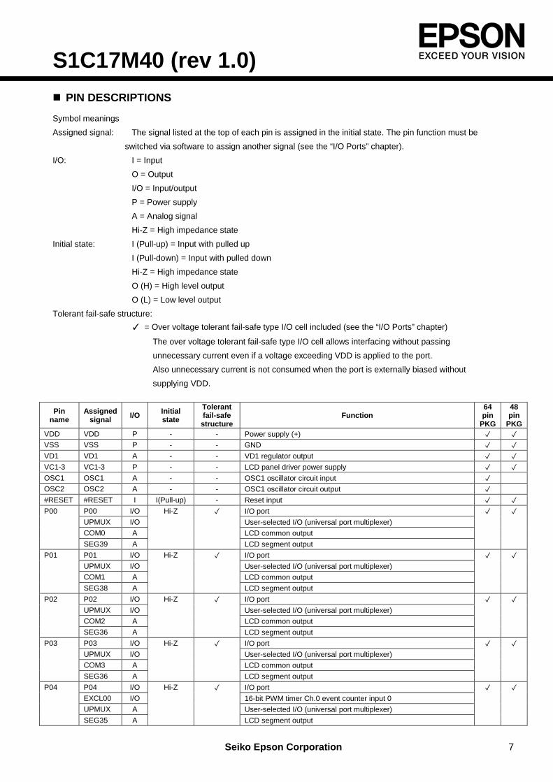
PIN DESCRIPTIONS Symbol meanings Assigned signal: The signal listed at the top of each pin is assigned in the initial state. The pin function must be
switched via software to assign another signal (see the “I/O Ports” chapter). I/O: I = Input
O = Output I/O = Input/output P = Power supply A = Analog signal Hi-Z = High impedance state
Initial state: I (Pull-up) = Input with pulled up I (Pull-down) = Input with pulled down Hi-Z = High impedance state O (H) = High level output O (L) = Low level output
Tolerant fail-safe structure: ✓ = Over voltage tolerant fail-safe type I/O cell included (see the “I/O Ports” chapter)
The over voltage tolerant fail-safe type I/O cell allows interfacing without passing unnecessary current even if a voltage exceeding VDD is applied to the port. Also unnecessary current is not consumed when the port is externally biased without supplying VDD.
Pin name
Assigned signal I/O Initial
state Tolerant fail-safe
structure Function
64 pin
PKG
48 pin
PKG VDD VDD P - - Power supply (+) ✓ ✓ VSS VSS P - - GND ✓ ✓ VD1 VD1 A - - VD1 regulator output ✓ ✓ VC1-3 VC1-3 P - - LCD panel driver power supply ✓ ✓ OSC1 OSC1 A - - OSC1 oscillator circuit input ✓ OSC2 OSC2 A - - OSC1 oscillator circuit output ✓ #RESET #RESET I I(Pull-up) - Reset input ✓ ✓ P00 P00 I/O Hi-Z ✓ I/O port ✓ ✓ UPMUX I/O User-selected I/O (universal port multiplexer) COM0 A LCD common output SEG39 A LCD segment output P01 P01 I/O Hi-Z ✓ I/O port ✓ ✓ UPMUX I/O User-selected I/O (universal port multiplexer) COM1 A LCD common output SEG38 A LCD segment output P02 P02 I/O Hi-Z ✓ I/O port ✓ ✓ UPMUX I/O User-selected I/O (universal port multiplexer) COM2 A LCD common output SEG36 A LCD segment output P03 P03 I/O Hi-Z ✓ I/O port ✓ ✓ UPMUX I/O User-selected I/O (universal port multiplexer) COM3 A LCD common output SEG36 A LCD segment output P04 P04 I/O Hi-Z ✓ I/O port ✓ ✓ EXCL00 I/O 16-bit PWM timer Ch.0 event counter input 0 UPMUX A User-selected I/O (universal port multiplexer) SEG35 A LCD segment output

S1C17M40 (rev 1.0)
8 Seiko Epson Corporation
Pin name
Assigned signal I/O Initial
state Tolerant fail-safe structure
Function 64 pin
PKG
48 pin
PKG P05 P00 I/O Hi-Z ✓ I/O port ✓ ✓ UPMUX I/O 16-bit PWM timer Ch.0 event counter input 1 SEG39 A User-selected I/O (universal port multiplexer) P06 P01 I/O Hi-Z ✓ LCD segment output ✓ ✓ UPMUX I/O I/O port SEG38 A 16-bit PWM timer Ch.1 event counter input 0 P07 P02 I/O Hi-Z ✓ User-selected I/O (universal port multiplexer) ✓ ✓ UPMUX I/O LCD segment output COM2 A I/O port SEG36 A 16-bit PWM timer Ch.1 event counter input 1 P10 P10 I/O Hi-Z ✓ User-selected I/O (universal port multiplexer) ✓ ✓ UPMUX I/O LCD segment output SEG23 A I/O port P11 P11 I/O Hi-Z ✓ User-selected I/O (universal port multiplexer) ✓ ✓ UPMUX I/O LCD segment output SEG22 A I/O port P12 P12 I/O Hi-Z ✓ User-selected I/O (universal port multiplexer) ✓ ✓ UPMUX I/O LCD segment output SEG21 A I/O port P13 P13 I/O Hi-Z ✓ User-selected I/O (universal port multiplexer) ✓ ✓ UPMUX I/O LCD segment output SEG20 A I/O port P14 P14 I/O Hi-Z ✓ User-selected I/O (universal port multiplexer) ✓ ✓ UPMUX I/O LCD segment output SEG19 A I/O port P15 P15 I/O Hi-Z ✓ User-selected I/O (universal port multiplexer) ✓ ✓ UPMUX I/O LCD segment output SEG18 A I/O port P16 P16 I/O Hi-Z ✓ User-selected I/O (universal port multiplexer) ✓ ✓ UPMUX I/O LCD segment output SEG17 A I/O port P17 P17 I/O Hi-Z ✓ User-selected I/O (universal port multiplexer) ✓ ✓ UPMUX I/O LCD segment output SEG16 A I/O port P20 P20 I/O Hi-Z ✓ User-selected I/O (universal port multiplexer) ✓ ✓ #ADTRG0 I LCD segment output UPMUX I/O I/O port SEG7 A 12-bit A/D converter Ch.0 trigger input P21 P21 I/O Hi-Z ✓ User-selected I/O (universal port multiplexer) ✓ UPMUX I/O LCD segment output SEG6 A I/O port

S1C17M40 (rev 1.0)
Seiko Epson Corporation 9
Pin name
Assigned signal I/O Initial
state Tolerant fail-safe structure
Function 64 pin
PKG
48 pin
PKG P22 P22 I/O Hi-Z ✓ I/O port ✓ UPMUX I/O User-selected I/O (universal port multiplexer) SEG5 A LCD segment output P23 P23 I/O Hi-Z ✓ I/O port ✓ UPMUX I/O User-selected I/O (universal port multiplexer) SEG4 A LCD segment output P24 P24 I/O Hi-Z ✓ I/O port ✓ ✓ UPMUX I/O User-selected I/O (universal port multiplexer) COM7 A LCD common output SEG3 A LCD segment output P25 P25 I/O Hi-Z ✓ I/O port ✓ ✓ UPMUX I/O User-selected I/O (universal port multiplexer) COM2 A LCD common output SEG43 A LCD segment output P26 P26 I/O Hi-Z ✓ I/O port ✓ ✓ UPMUX I/O User-selected I/O (universal port multiplexer) COM1 A LCD common output SEG42 A LCD segment output P27 P27 I/O Hi-Z ✓ I/O port ✓ ✓ UPMUX I/O User-selected I/O (universal port multiplexer) COM0 A LCD common output SEG41 A LCD segment output P30 P30 I/O Hi-Z ✓ I/O port ✓ ✓ UPMUX I/O User-selected I/O (universal port multiplexer) CP1 A LCD power supply booster capacitor connect pins P31 P31 I/O Hi-Z ✓ I/O port ✓ ✓ UPMUX I/O User-selected I/O (universal port multiplexer) CP2 A LCD power supply booster capacitor connect pins P32 P32 I/O Hi-Z ✓ I/O port ✓ RTC1S O Real-time clock 1-second cycle pulse output UPMUX I/O User-selected I/O (universal port multiplexer) P33 P33 I/O Hi-Z ✓ I/O port ✓ ✓ LFRO O LCD frame signal monitor output UPMUX I/O User-selected I/O (universal port multiplexer) VREFA0 A "12-bit A/D converter Ch.0 reference voltage input,
constant voltage output"
P34 P34 I/O Hi-Z ✓ I/O port ✓ ✓ EXOSC I Clock generator external clock input UPMUX I/O User-selected I/O (universal port multiplexer) ADIN0 A 12-bit A/D converter Ch.0 analog signal input 0 P35 P35 I/O Hi-Z ✓ I/O port ✓ ✓ UPMUX I/O User-selected I/O (universal port multiplexer) ADIN1 A 12-bit A/D converter Ch.0 analog signal input 1
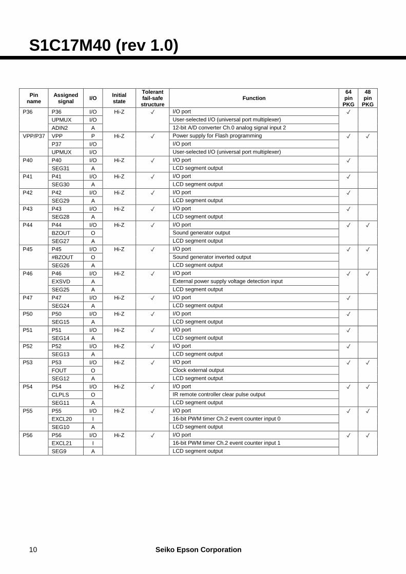
S1C17M40 (rev 1.0)
10 Seiko Epson Corporation
Pin name
Assigned signal I/O Initial
state Tolerant fail-safe structure
Function 64 pin
PKG
48 pin
PKG P36 P36 I/O Hi-Z ✓ I/O port ✓ UPMUX I/O User-selected I/O (universal port multiplexer) ADIN2 A 12-bit A/D converter Ch.0 analog signal input 2 VPP/P37 VPP P Hi-Z ✓ Power supply for Flash programming ✓ ✓ P37 I/O I/O port UPMUX I/O User-selected I/O (universal port multiplexer) P40 P40 I/O Hi-Z ✓ I/O port ✓ SEG31 A LCD segment output P41 P41 I/O Hi-Z ✓ I/O port ✓ SEG30 A LCD segment output P42 P42 I/O Hi-Z ✓ I/O port ✓ SEG29 A LCD segment output P43 P43 I/O Hi-Z ✓ I/O port ✓ SEG28 A LCD segment output P44 P44 I/O Hi-Z ✓ I/O port ✓ ✓ BZOUT O Sound generator output SEG27 A LCD segment output P45 P45 I/O Hi-Z ✓ I/O port ✓ ✓ #BZOUT O Sound generator inverted output SEG26 A LCD segment output P46 P46 I/O Hi-Z ✓ I/O port ✓ ✓ EXSVD A External power supply voltage detection input SEG25 A LCD segment output P47 P47 I/O Hi-Z ✓ I/O port ✓ SEG24 A LCD segment output P50 P50 I/O Hi-Z ✓ I/O port ✓ SEG15 A LCD segment output P51 P51 I/O Hi-Z ✓ I/O port ✓ SEG14 A LCD segment output P52 P52 I/O Hi-Z ✓ I/O port ✓ SEG13 A LCD segment output P53 P53 I/O Hi-Z ✓ I/O port ✓ ✓ FOUT O Clock external output SEG12 A LCD segment output P54 P54 I/O Hi-Z ✓ I/O port ✓ ✓ CLPLS O IR remote controller clear pulse output SEG11 A LCD segment output P55 P55 I/O Hi-Z ✓ I/O port ✓ ✓ EXCL20 I 16-bit PWM timer Ch.2 event counter input 0 SEG10 A LCD segment output P56 P56 I/O Hi-Z ✓ I/O port ✓ ✓ EXCL21 I 16-bit PWM timer Ch.2 event counter input 1 SEG9 A LCD segment output

S1C17M40 (rev 1.0)
Seiko Epson Corporation 11
Pin
name Assigned
signal I/O Initial state
Tolerant fail-safe structure
Function 64 pin
PKG
48 pin
PKG P57 P55 I/O Hi-Z ✓ I/O port ✓ SEG8 A LCD segment output P60 P60 I/O Hi-Z ✓ I/O port ✓ ✓ COM3 A LCD common output P61 P61 I/O Hi-Z ✓ I/O port ✓ ✓ COM2 A LCD common output P62 P62 I/O Hi-Z ✓ I/O port ✓ ✓ COM1 A LCD common output P63 P63 I/O Hi-Z ✓ I/O port ✓ ✓ COM0 A LCD common output PD0 DST2 O Hi-Z On-chip debugger status output ✓ ✓ PD0 I/O I/O port ADIN3 A 12-bit A/D converter Ch.0 analog signal input 3 PD1 DSIO I/O I(Pull-up) On-chip debugger data input/output ✓ ✓ PD1 I/O I/O port PD2 DCLK O O(H) On-chip debugger clock output ✓ ✓ PD2 O Output port
Universal port multiplexer (UPMUX) The universal port multiplexer (UPMUX) allows software to select the peripheral circuit input/output function
to be assigned to each pin from those listed below. Peripheral circuit Signal to be assigned I/O Channel number n Function
Synchronous serial interface (SPIA)
SDIn I n=0,1 SPIA Ch.n data input SDOn O SPIA Ch.n data output SPICLKn I/O SPIA Ch.n clock input/output #SPISSn I SPIA Ch.n slave-select input
I2C (I2C)
SCLn I/O n=0 I2C Ch.n clock input/output SDAn I/O I2C Ch.n data input/output
UART (UART3)
USINn I n=0,1,2 UART Ch.n data input USOUTn O UART Ch.n data output
16-bit PWM timer (T16B)
TOUTn0/CAPn0 I/O n=0 T16B Ch.n PWM output/capture input 0 TOUTn1/CAPn1 I/O T16B Ch.n PWM output/capture input 1
IR remote controller (REMC)
REMO
O
n=0
IR remote controller transmit data output
Note: Do not assign a function to two or more pins simultaneously.
S1C17M40 (rev 1.0)
12 Seiko Epson Corporation
Document code: 413875400 Issue August 2019 in JAPAN
NOTICE: No part of this material may be reproduced or duplicated in any form or by any means without the written permission of Seiko Epson. Seiko Epson reserves the right to make changes to this material without notice. Seiko Epson does not assume any liability of any kind arising out of any inaccuracies contained in this material or due to its application or use in any product or circuit and, further, there is no representation that this material is applicable to products requiring high level reliability, such as, medical products. Moreover, no license to any intellectual property rights is granted by implication or otherwise, and there is no representation or warranty that anything made in accordance with this material will be free from any patent or copyright infringement of a third party. When exporting the products or technology described in this material, you should comply with the applicable export control laws and regulations and follow the procedures required by such laws and regulations. You are requested not to use, to resell, to export and/or to otherwise dispose of the products (and any technical information furnished, if any) for the development and/or manufacture of weapon of mass destruction or for other military purposes. All brands or product names mentioned herein are trademarks and/or registered trademarks of their respective companies. Seiko Epson Corporation 2019, All rights reserved
Sales & Marketing Division
Seiko Epson Corporation
Device Sales & Marketing Department 421-8 Hino, Hino-shi, Tokyo 191-8501, JAPAN Phone: +81-42-587-5814 FAX: +81-42-587-5116
global.epson.com/products_and_drivers/semicon/
EPSON semiconductor website