s m sze solution
TRANSCRIPT

ch.lch.2ch.3ch.4ch.5ch.6ch.7ch.8ch.9ch.10ch. r lch.t2ch. 13ch.r4
ContentsIntroductiorr----- --- 0Energy Bands and Carrier Concentration ICarrier Transport Phenomena ------ ---- 7p-n Junction ----- --- 16Bipolar Transistor and Related Devices- --------- 32MOSFET and Related Devices--------- ---------- 48MESFET and Related Devices------- -- 60Microwave Diode, Quantum-Effect and Hot-Electron Devices ----- 68
Photonic Devices ---------- ----------- 73Crystal Growth and Epitaxy------Film Formation------ -- 92Lithography and Etching ---- 99Impurity Doping-- - 105Integrated Devices--------- -- l 13

CHAPTER 2
1. (a) From Fig. llq the atom at the center of the cube is surround by four
equidistant nearest neighbors that lie at the corners of a tetrahedron. Therefore
the distance between nearest neighbors in silicon (a: 5.43 A) is
l/2 [(a/2)' * (Jzo /2127t/' : J-zo /4 : 235 A.
(b) For the (100) plane, there are two atoms (one central atom and 4 corner atoms
each contributing ll4 of an atom for a total of two atoms as shown in Fig. 4a)
for an area of d, therefore we have
2/ &:2/ (5.43 ,. l0-8)z :618 * 10la atoms / crt
Similarly we have for (110) plane (Fig. 4a and Fig. 6)
(2+2x l l 2+4x l l 4 ) / JTo2 :9 .6 , . 10 rs a toms / c r1 � . ,
and for (111) plane (Fig. 4aand Fig. 6)
(3 x I/2+ 3 x r/6) / rlz|mlf ,ffi" I : : 7.83 * 10la atoms / crrt.(9.
2. The heights at X, Y, and Z point are /0, %,^O %.
3. (a) For the simple cubic, a unit cell contains 1/8 of a sphere at each of the eight
corners for a total of one sphere.
- Ma><imum fraction of cell filled
: no. of sphere x volume of each sphere / unit cell volume
:1x 4ng /2 )3 l a3 :52o /o
(b) For a face-centered cubic, a unit cell contains 1/8 of a sphere at each of the
eight corners for a total of one sphere. The fcc also contains half a sphere at
each of the six faces for a total of three spheres. The nearest neighbor distance
is l/2(a J; ). Therefore the radius of each sphere is l/4 1a Jz ).
- Maximum fraction of cell filled
- (1 + 3) {4[ [(a/2) / 4It I 3] / a3 :74o/o.
(c) For a diamond laffice, a unit cell contains 1/8 of a sphere at each of the eight
corners for a total of one sphere, I/2 of a sphere at each of the six faces for a
total of three spheres, and 4 spheres inside the cell. The diagonal distance

between (112,0, 0) and (114, ll4, Il4) shown in Fig. 9a is
The radius of the sphere isDl}: 1Jj8- Maximum fraction of cell filled
: (t + 3 + 4) lyErtj l ' 'o, :nJT t16 : 34 %.' 1 3 \ 8 ) )
This is a relatively low percentage compared to other lattice structures.
4. la,l : la,l : la,l: laol : a4 *4+4+4 :o4 . ( 4 * 4 + 4 * 4 ) : 4 . o : ola, l ' *4 -4 *4.4 + 4. L: o
--d2+ d2 coflrz + dcoiln I dcoflr+ ! dz +3 d2 coil! 0
- coil: +[: cos-r
+ [ 109.4/ !
5. Taking the reciprocals of these intercepts we get ll2, ll3 and l/4. The smallest
three integers having the same ratio are 6, 4, and 3. The plane is referred to as
(643) plane.
6. (a) The lattice constant for GaAs is 5.65 A, and the atomic weights of Ga and As
are 69.72 and 7 492 glmole, respectively. There are four gallium atoms and
four arsenic atoms per unit cell, therefore
4/a3 : 4/ (5.65 x 10⁻⁸)3 : 4.22 x lTn Ga or As atoms/cr*,Density: (no.of atoms/crrf x atomic weight) / Avogadro constant
: 2.22 * 1022(69.72 + 74.92) I 6.02* 1023 : 5.33 g I cni.
(b) If GaAs is doped with Sn and Sn atoms displace Ga atoms, donors are
formed, because Sn has four valence electrons while Ga has onlv three. The
resulting semiconductor is n-type.
7. (a) The melting temperature for Si is l4l2 oC, and for SiOz is 1600 oC. Therefore,
SiOz has higher melting temperature. It is more diflicult to break the Si-O
bond than the Si-Si bond.
(b) The seed crystal is used to initiated the growth of the ingot with the correct
crystal orientation.
(c) The crystal orientation determines the semiconductor's chemical and electrical
; ) ' . ( ; ) 'n : 1
2

properties, such as the etch rate, trap density, breakage plane etc.
(d) The temperating of the crusible and the pull rate.
4.73x10u T'ErQ): l . l7 for Si
. '. Es ( 100 K) = 1.163 eV, and Es(600 K): 1.032 eV
E,(D= r.5 ,n -t'o-l!j_"t!1,!' ror GaAs(T + 204)
,.Er( 100 K) : 1.501 eV, and Es (600 K) : 1.277 eY .
9. The density of holes in the valence band is given by integrating the product
N(E)tl-F(DldE from top of the valeri c:e band (En taken to be E : 0) to the
boffom of the valence band Rottoml
p: ytu'�n^ N(qtl _ F(DldE
where I -F(E): I - { t r [ t * "(t-
Ee)*t ] : [ t *"(E-Eilr t ' r l t
If Er- E >> kT then
| - F(E) - exp F (n, - r)lwl e)Then from Appendix H and, Eqs. I and 2we obtain
p : 4Df2mp / h2f3D I:""^ EtD exp I-@r - E) / kT ldE (3)
Letxt+ E lkT, and let Ebooo*: - @, Eq.3 becomes
p : 4\-2mo / rtflz (kTlttz exp [-(Ep / kl)i I xtD e*dx
where the integral on the right is of the standard form and equats G tZ.- p :2l2Dmo kT / h213D exp [-(Ep / kI)j
By refening to the top of the valence band as ETinstead of E:0 we have
or p:2Qo';f:"i1ff;Trrlf;, u, /krl
where Nv:2 (Nmo kT / rtf .
10. From Eq. 18Nv :2QDmo kT I h2f D
The effective mass of holes in Si is
mp -- (Nvt 21ztt (rt tzDkT)
( 1 )
1.38 x 10-233oo): 9.4 " 10-3 t kg : 1.03 mo.
Similarly, we have for GaAs
f f ip :3 .9 x 10-31 kg: 0 .43 mo.
Using Eq. 191 1 .

E i = (8, + til' . (%)^ (N, I w,)
= (Ec* Ey)l 2 + (*T I 4) ln
A t77 KE,: (1.t6/2) + (3 x 1.3g x t}-,tT) / (4 x 1.6 x 10-,r) ln(l.0/0.62)
:0.58 + 3.29 x 10⁻⁵ Z= 0.5g + 2.54 x 10⁻³ - 0.5g3 ev.At 300 K
Ei: (1.12/2) + (3.29 x 10-sX300; : 0.56 + 0.009 : 0.569 eV.At 373 K
Ei: (1.0912) + (3.2g x l0-sx3731 - 0.545 + 0.012:0.557 ey.Because the second term on the right-hand side of the Eq.l is much smaller
compared to the first term, over the above temperafure range, it is reasonable to
assume that Ei is in the center of the forbidden gap.
"-@-r rYw 6B
l '=rr-rr,
lr*,1*,)(o%f (1 )
I : :@_ECT2. KE :
1 3 .
f : JE -Er"-@-tP)/*r6P
1 . 5 x 0 . 5 " G
0.sJ;
?= ;or.
(a) p: f tw:9.109 x 10-3r x105 :9.109 x 10⁻²⁶ kg-mA
1 : h - 6 '626x10-14- :7 .27 x r0-e m:72.7 Ap 9.109 x l0- ' "
m ^ ^ I(b) 1" 'L : *x 72.7: I154 A ."
m p 0.063
From Fig.22when nr: l0t5 cd3, the corresponding temperature is 1000 / T: l.B.
So that I : 1000/1.8:555 K or 282 [
From E" - Er: kT lnlNc / (No - N,q)]which can be rewritten as No - N.e: l/c exp IaE, - Er) I kf IThen No-N.a:2.86 * 10re exp(-0.20 /0.0259): 1 .26 x 1016 crn3
o r No :1 .26x 1016+ N . t : 2 .26 * 1016c rn3A compensated semiconductor can be fabricated to provide a specific Fermi
energy level.
16. From Fig.28a we can draw the following energy-band diagrams:
14.
1 5 .

AT 77K Ec(0.ssevi'EF(0.s3)
E;(o)
Ev(-0.59)
Ec(0.56 ev)
EF(0.38)
Ei (o)
Ev(-0.56)
E9(0.50eV)
AT 3OOK
ri
AT 6OOK
0.s0)
17. (a) The ionization energy for boron in Si is 0.045 eV. At 300 K, all boronimpurities are ionized. Thus pp: N.a: l0ls crn3
np: t?i2 / n.a: (g.6i " K;9f / l}ts :9.3 * lOa crn3.
The Fermi level measured from the top of the valence band is given by:
Ep- Ev: kTln(N/ND):0.0259ln(2.66 x 10re / l0r5; :0 .26 eY
(b) The boron atoms compensate the arsenic atoms; we have
p p : N e _ N n : 3 x 1 0 1 6 _ 2 . 9 x l 0 1 6 : l O l s c r n 3Sincepo is the same as given in (a), the values for no and Ep are the same asin (a). However, the mobilities and resistivities for these two samples are
different.
18. Since Np >> ni, wa can approximate e : Nt andpo: n? I no:9.3 x l } te I l0 l7 : 9 .3 x ld crn3
( p - r ' \From fio: txiexP I
"t "' | '
\ . kT ) 'we have
Ep - Ei: kT ln (no I n) : 0.0259 ln (1017 / 9.65 * 10e) : 0.42 eYThe resulting flat band diagram is :

E c
EF
A.rr2eY
- E - F .t - l
19. Assuming complete ionization, the Fermi level measured from the intrinsic
Fermi level is 0.35 eV for 10rscm-3,0.45 eV for 1017 crn3, and 0.54 eV for 10le
crn3.
The number of electrons that are ionized is given by
n = Npfl - F(En)l: Np / f l + "-(ro-rr)r*r ]Using the Fermi levels given above, we obtain the number of ionized donors as
l1.12 eV
l
20. No* -
Therefore, the assumption of complete ionization is valid onty for the case of10ls crn3.
10 tu 1016: _l + e - {Eo -E r ) / k r 1 +e -0 .13s
n: !0 t5 crn3n: 0.93 * 1017 crn3n :0 .27 * lO le c rn3
:5 .33 t 10 ls c rn3
for Na : 1015 crn3forNo: 1017 crn3forNo: 10le crn3
_ l 0 t u
. l
1 . t45The neutral donor: 1016- 5.33 ,. l0ls crr3 : 4.67 x 10¹⁵ crn3
-The ratio of N; - 4'76 - 0.g76N; s.33

CHAPTER 3
I . (a) For intrinsic Si, /4, : 1450, l+ :505, and n: p : lti:9.65x lOe
We have p - - 3.31x 10' C)-cmqntth + {lpltp en,(lt, + pr)
(b) Similarly for GaAs, lh: 9200, Lb : 320, and n: p : ni:2.25x10⁶
We have p - = 2.92x lOt O-crnqnltn + llPIIp
For laffice scatteri nE, l-h n 73/2
en,(ltn + po)
2.
3. Since
1 1 1- = - + -p 250 500
Fr : 1 67 cr# N-s.
4. (a) p:5x l01s cd3, n: n / /p : (9 .65x l0e12l5x10rs : 1 .86x104 cm-3
14:4lo cm2lv-s, Lh:1300 cm2lv-s
r3oox #:2388
cm2lv-s
T : 4oo K, 1^4,: l3oox % : 844 "m'lv-s.300-rt
2
r I :3 C)-cm
T : 200 K, Lh:
l l l- = - + -P l-t' l-t"
p :qpon + qlrpp qppp
( b ) p : N t - N o : 2 x 1 0 1 6 - 1 . 5 x 1 0 1 6 : 5 x 1 0 l t " * ' , n : L 8 6 x 1 0 a c m - 3
!-b: Ib (M + No) : I+ (3.5xl0tu) :290 cm2A/-s,
fh: th(Nt + Np): 1000 cm2ny'-s
= | :4.3 C)-cmp
qLthn + q[Lpp qppp

6.
(c) p:N,q @oron) -Nn+ N,q(Gal l ium):5x10ls cd3, n: L86xl0a cm-3
I+: I$ (M r Np* Ne): 14 Q.05x10tt) : 150 cm2A/-s,
l-h: th (Ne * Np* N,q) : 520 crr?A/-s
p:8.3 C)-cm.
5. Assume No- N1>> n;,the conductivity is given by
ox qn[h: elh(No - Nd)
We have that
16 : (1.6x tOae)1^6Qtp- 10tt)
Since mobility is a function of the ionized impurity concentration, we can use
Fig. 3 along with trial and error to determine 7^6, and No. For example, if we
choose No : 2xl0r7,then Nr : ND* + Nd- : 3x lQtt, so that Lh x 510 cm2lV-s
which gives o: 8.16.
Further trial and effor yields
Nn=3.5x10¹⁷ crrt .3
and
lh x 400 cm2lV-s
which gives
6x 16 (O-cm)-t
o- q(lt n + Fo p) = ello(bn + ni t n1
From the condition dddn: 0. we obtain
f t :n i I {b
Therefore

i . At the limit when d >> s, CF: :4.53. Then from Eq. 16
0.226 x 10-' - 10.78 mV.50x10-o x4 .2
R u =V,A 1 0 x 1 0 - 3 x 1 . 6 x l 0 - 3 - 426.7 cnf tCIB ,W 2 .5x l0 -3 x (30x10-n x l0o )x0 .05
Since the sign of R'7 is positive, the carriers are holes. From Eq.22
V l0 x l0 -3p = i x W x C F - x 5 0 x 1 0 - 0 x 4 . 5 3 - 0 . 2 2 6 C ) - c m
From Fig. 6, CF:4.2 (d/s: 10); using the a/d: 1 curve we obtain
p * _ q i o ( b n , l 4 b + ^ , l b n , ) _ b + lP, 2JE
QFpni(D + l)
= 380 cm2lv-s.Wp 1 .6x10 - ' n x1 .46x10 '6 x1 .1
7C
lnz
V = p . I / ( W . C F ) _
8. Hall coefficient,
l l 1
' eR, l , .6xl0- 'n x426.7
Assuming Ne x p, from Fig. 7 we obtain p: 1.1 f)-cm
The mobllity pg is given by Eq. 15b
1I: - =p,
9. Since R n pand p-qnph + wl_rp
From Einstein relation D n lt
, hence R o. 1
. nl+ + pLrp
H l l r o = D n l D o - 5 9

R , _
0.5Rr
We have N.e:50 Nn .
N olt^
N o l t , + N e q p
10. The electric potential @is related to electron potential energy by the charge (- q)
IQ:*=(Er_ n i )
q
The electric field for the one-dimensional situation is defined as
e(x) : -!!-: l dEid x q d x
( n- - n \ft: ni explT): No(x)
Hence
l l .
E p - E ; : k T h ( * r @ )
l . )
E &) - -( tt\ t dN o(x)\ q ) N o ( * ) d x
(a) From Eq. 31, Jn:0 and
r (x) - - D, d/d* - - kT No!:a)9- " - *kT o
H n q N o " n ' q
(b) E (r): 0.0259 (100) :259 V/cm.
At thermal and electric equilibria,
J , = qgn(x)e + qD, 4:!') -,dx
12.
Dn I dn(x) D, N, -f f .
LE ( x ) =
F,
- - D n
p,
n(x) dx Lt,
N , -NoN o * ( N r - N ' ) ( * l L )
L N o + ( N , - N o ) t
l 0

t , - [ ' - D"
J o p
I\a) Tp =
oor,rry =
N, -No- -o -nNL
LNo + (N, - N, )r p" N,
13. Nt = Lp - ToG, = 10 x 10-6 x l0 tu = 10t t crn3
f l : f t no + Ln :No + Ln :10 I s +10 t t - 19 t s c rn3
n? e.65 x lon ) ' + lor , = lo, , cm-,p - \ + 4 p = 1 0 "
t4 .5 x l 0 - t 5 x 1 0 7 x 2 x l 0 t s
f ln = tlno, Pn = Pno
= 10- t s
10-8 x 20
3 x 1 0 - a + 1 0 - 8 x 2 0
- 3 x 1 0 { c m
Sr, : v,r,o,N,,, - 107 x 2x 10-t6 x 10to - 20 cm/s
(b) The hole concentration at the surface is given by F,q.67
p ̂ (o) = pno + roG rlt -, "11'-
I\
u p * T o S , , )
_ (9.g5 1 l9_') ' + 10-, *t0,,( t _2 xl}tu (.
= lOe cm-'.
6= QnLIt, * wqy
Before illumination
1 5 .
After illumination
f l n = f r n o * L r t - f t r o * T r G ,
p n = p n o * L p - p n o * t r G
Ao - tqtt,(nno * Ln) + qlrp(p," + 4p)] - (qlt n," * QFo p,")
- q(l+ + Fp)r oG .
l l
9 x 10⁻⁸D oTo

ta) J r .a in - -nD r#
- - l.6x 10-lex IZx . - l-
x l0rsexp (-x/12)L2xl0-"
: 1.6exp (-x/12) Alcrrl
(b) / " ,dr i f t = J,o,o,-Jp,ain
: 4.8 - 1.6exp(-x/12) Alcni.
(c) 't Jn.a,in - qnl+E
- '- 4.8 - l.6exp(-xll2): 1.6x 10-1ex 1016x 1000x8
E :3-exp(-x/t2) V/cm.
1 7 . F o r E : 0 w e h a v e
a _ _ P n _ P n o + D , I * = g0t tp o Ax'
at steady state, the boundary conditions are p" @ - 0) : p" (0) and pn (, : lV) :
Pno.
Therefore
'*[fj'*F)
J r(x- o) : - QDp H,.- q[.p,(o) - o,"l+-4+)
J o(x -w) = - QD.H,=, - ql.p
18. The portion of injection current that reaches
T2
p,(x)= pno +[1t , (0)- p^.
n,(o)- p^,1?4.
'o ,inhf w I
lL, )
the opposite surface by diffirsion IS

given by
a $ =J o(W)JoQ) cosh(W lLe)
Lo = ̂ t ' r%= '& tso* to* -5x lo -2 cm
; . d o - - 0.98cosh(10-2 /5x 1O-' �)
Therefore,9SYo of the injected current can reach the opposite surface.
19. In steady state, the recombination rate atthe surface and in the bulk is equalAPr,ou,u
- LPn,"urf^u
so that the excess minorirv " *i:;:*..J#'ff at the surface
;,,surrace : lora. :g :1013 cm-3- 1 0 - o
The generation rate can be determined from the steady-state conditions in thebulk
G: lo to : lom crn3s- ll 0 - 6
From Eq. 62, we can write
D ^ a ' L ! + G - & : o" Axt To
The boundary conditions are 4(. = - ): l01a crn3 and 4(* - 0): 1013 crn3
Hence
where
4(i: lola( 1 - o.ge-' t to )
Lp:.f io- to-u : 31.6 pm.20. The potential barrier height
Qa = Q^ - X: 4.2 - 4.0:0.2 volts.The number of electrons occupying the energy level between E and E+dE isdn: N(DF(DdEwhere N(E^) is the density-of-state function, and F(E) is Fermi-Dirac distributionfunction. Since only electrons with an energy greater than E, + eQ^ and havinga velocity component normal to the surface can escape the solid, the thermioniccurrent density is
- | r- +Az.T)% v,E%e-G-rr)ln 4gJ -- JQt,
= Jrr*qq^ ht
'
where v, is the component of velocity normal to the surface of the metal. Sincethe energy-momentum relationship
n P 2 I . ) ) ? rE - -2m 2m
2 t .
l 3

Differentiation leads to dE - PdP
mBy changing the momentum component to rectangular coordinates,47iP2 dP - dp,dp ,dp "
f - Z? , S f [- p ,u-'ol
* p2,+ p]-z^t1) lzmkr dp ,dp ,dp ,
Hence =Ht',
^t'r'-,;t,'^rl')u,, o,oo,ll- ,-01r,^0, dp, f- ,-r)/z^kr dp,mht J p,o
where p',o = Zm(E, + qQ).
l E t " l l 2
Since L e-o" dx -{ ll , the last two integrals yield (2dmkT)v'� .\ a )
The first integral is evaluated by setting oi:'9' - u
Therefore we have du - P'dP'
2mkT
mkTThe lower limit of the first integral can be written as2m(E, +qQ)-2mE, _qQ*
2mkT kT
so that the first integral becomes mkT fr^,0,
e-" du - mkT e-qL-l kr
Hence , -4tqmkz 72o-a0^lk, - A*7, "*(-fg^\h ' \ k T )
22. Equation 79 is the tunneling probability
r _ { t * [ 2 0 x s i n h ( 2 . 1 7 x l 0 o x g x t o - ' o ] ' ] : 3 . r 9 x l 0 * .L 4 x 2 x ( 2 0 - 2 ) )
23. Equation 79 is the tunneling probability
p -
r '0-,0) - { , * [6x sinh( 9.99 x 10n x 10-'o)f ]- ' _ 0.403
L 4 x 2 . 2 x ( 6 - 2 . 2 ) )
Tr0-\ _ {r * [o * rinh (q.qq :. ro' *lo-'l ' ]- ' = 7.8 x r0-,.'
L^ '
4 x2.2"(e -z.z) l
t4

Differentiation leads to dE = PdP
mBy changing the momentum component to rectangular coordinates,47d, 2 dp : dp,dp ,dp "
Hence t = +[, [=- [ l =*o,r-rr2'+pi+p2,-znr1)' '^o' dp,dp rdp "
= ,r2o ff,,
"to'-'^Et)l2^tr p,dp,!-_ "-oll'^o'dp, f* "^o1/'^0, dp,
rvhere p'�,o = 2m(E, + eQ).r : l l 2
r' *' - =[ Z1 , the last two integrals yield (2dmk|)v, .Srnce J__ e-"^ dx \" )
The first integral is evaluated by setting pi;29' :, .
2mkT
Therefore we have 4y - P'dP'mkT
The lower limit of the first integral can be written as2m(E, +qQ)-2mEo =qQ.
2mkT kT
so that the first integral becomes *0, fr^,o
e-" du: mlsT s-tQ./ kr
Hence 1 =4tq*k' 72"-t0^lw = A'7, "*"( - uh).-
h 3 -
k r ) '
ll. Equation 79 is the tunneling probability
o _ l2* , (qVo - E) _P_t l - - - - - - - - - - ' i -_
2(9. l Ix t0_3 'x20 -2)(1.6x 10- 'e)= 2 . 1 7 x 1 O t o m - t(1.054x 10- 'o ) t
) - ' = r . ,n , ,0 *, - lr- [20 x sint( 2.17 x 100 x 3 x 10-'o] '
r - \ r
| 4 x2 x (20 -2 )
13. Equation 79 is the tunneling probability
B =
r '0-,0) = {r* [6x sintr( 9.99 x10' x10-'o)I ] = o.oo,
| . 4 x2 .2x(6 -2 .2 ) )
r '0 -n l = [ * [o* r inh (q .qq I ro ' * lo - ' l ' I ' = 7 .8x l0 -e .'
l ' ' 4 x 2 . 2 " ( a - z . z ) J - '

24.From Fig. 22A s s : 1 0 3 V / s
ua = l.3xl06 cm/s (Si) and ua x 8.7x106 cm/s (GaAs)
t x 77 ps (Si) and t x 11.5 ps (GaAs)
As E :5x10⁴ V/s
va x 107 cm/s (Si) and, ua x 8.2x106 cm/s (GaAs)
t x l0 ps (Si) and t = l2.2ps (GaAs).
25. Thermal velocitv
= 9.5 x 10n m/s = 9.5 x 10u cmlsFor electric field of 100 vlcm, drift velocity
v a = l_4,E = 1350 x 100 = 1.35 x 105 cm/s << v,,
For electric field of 104 V/cm.
FoE = 1350 x 104 = 1.35 x 107 cm/s = y,r, .
The value is comparable to the thermal velocity, the
drift velocity and the electric field is not valid.
linear relationship between
2 x|.38 x 10-2' x 300

CHAPTER 4
l. The impurity profile is,
(Np-N,a) (cm")
3x lOra
x (pm)
The overall space charge neutra
c :101e cm-a
of the semiconductor requires that the total negative
space charge per unit area in the p-side must equal the total positive space charge per
unit area in the n-side, thus we can obtain the depletion layer width in the n-side region:
0 . 8 x 8 x 1 0 ' o- Wn x3 x 10 'o
Hence, the n-side depletion layer width is:
W, =1.067 pm
The total depletion layer width is 1.867 pm.
We use the Poisson's equation for calculation of the electric field n(x).
In the n-side region,
L = 3 - * r + r ( x ^ ) = L N o x + Kd x t " " E s
E ( x , = 1 . $ 6 7 F m ) = O + K = - + N , x l . 0 6 7 x 1 0 - a€.,
" ' E ( t , \ = L * 3 x l o r a ( x _ � l ' 0 6 7 x l o r )E
E ̂o, =E ( x, = 0 )= -4. 86 x 103 V/cm
In the p-side region, the electrical field is:

9=L*^ =e (x " ) = =n rax2 + K 'dx t r P ' 2€ ,
E (x p = _0.81m) :0 + K ' =- t * o*(0.S" t0-o) '
. . , G") :a *o, l * ' - (o.s, , ro- ' ) ' l\ P ' 2 t , L ' ' )
E,o, =E (ro =0) = -4.86 x 10³ V/cm
The built-in potential is:
v,, = - I _:,, &W = - l'0,,, (r)d*l o _,,0" _�l;", (')4 n _s ide =0.s2 v .
L From Vo, = - J
r (*V, , the potential distribution can be obtained
With zero potential in the neutral p-region as a reference, the potential in the p-side
depletion region is
v,(,) = - li e)a* = - ft * o *l'- (o.r x 10' )'f* = -ftLir - (o.s * r0-o)' " -l{o rx 10 0
= -7.5e6x 10" x [1"'
- (0.r, ro-') ' * -?r(0.t,. to- ') ' ]
With the condition Vp(0):V"(0), the potential in the n-region is
v^&) = -t":' ro''[]"' -t.o67xro-ax.UF,.ro-')
= -4.56xr0' "()* -1.067x lo-ox T,.
,o-')

[[-
!!- )D---lr-
l[_ l l . - , .!_-.[.-_
m_ l!_.- n!
!m l[ n__tr- ,
[!- l ! , f l _
-____t ,_[[^ l!-
-^-[-m_ l![[--
l--
!!t [ [ [ . . ,__fl-
l[l-_J_t--
---l[- t![. f____ r
["Jr][+n_Jo_!{

i. The intrinsic carriers density in Si at different temperatures can be obtained by using Fig22 in
Chapter2:
Temperature (K) lntrinsic carrier density (n,)
250 1.50+108
300 9.65+10'
350 2.oo+10"
400 8.50]l10''�
450 9.00+10'3
500 2.20+10t4
The Vu can be obtained by using Eq.12, and the results are listed in the following table.
J! --lmIml 
+. .E- - . = lz rn ( .y^*+ ) - l " '=4xr0s- f2x t .6x l0 ' ' x30 [ '9 ] ' t , ) l ' "m u
L e [ N r * N r ) ) [ l t . e x 8 . 8 5 x l 0 - ' o [ 1 0 ' ' + N " ) ]
> 1 .755x 10 tu = N D
r + #
We can select n-type doping concentration of Nr: 1.755x10t6 crnt for the iunction.
5. From Eq. 12 and Eq. 35, we can obtain the l/C2 versus Zrelationship for doping concentration of
l0't, 10t6, or lOtt crn3, respectively.
ForNr:16r5 "*-:,
+= 'V : ,
_ ' ) - zx (o .s t t -v ) -=1 .187x 10 ,6 (o . tz t -v )C , ' Q d " N u 1 . 6 x 1 0 - ' n x l l . 9 x 8 . 8 5 x 1 0 - ' n x l 0 '
For No:19r6 "*-:,
c , ' e d " N u l . 6 x 1 0 - r e x 1 1 . 9 x g . g 5 x l 0 - , 0 ; 1 0 " = 1 ' 1 8 7 x t o " ( o ' s l o - r )
For Nlr:1017 crn3,
I _ zVu, -v) _ zx(o.gsa-v)C , ' 4 d , N u l . 6 x l 0 - l 9 ' t t f f i = L . | 8 7 x t o ' o ( o . e s o - r , )
When the reversed bias is applied, we summarize atable of I /Ct, vs V for various Np values asfollowing,

[_ l!.-._lI [[_-*JI'-l
l! , - fl-l
Lt__-[[ x. fr!L-
] [ , . f l t._n
l ! . f [n-
3r nl![[!_ rr__Jm. f-l
n n m
[-JD TIT]4U/4U iL__.__.![
.-nn . n n n
[ " __[-_.nn-
__-!-_ul.-n
D[!!D[-
[. nD -n.^---_ln.
_J____-[!--!
_ nn. n[[_
! * .--8.-.-D[-
J_n._nl._n
n n n1!J1_!U
mm ._-[!__^-l! -_rJJil--[
-i--m
! ][l [
The interceptions give the built-in potentialof thep-n junctions.

6. The builrin potential is
2 k T , ( a ' e " k r \ ? (Vr , :=- ln l - - i ; l= i *0 .0259x h l" ' 3 q \ \ q ' n i ) 3 t= 0.5686 V
From Eq. 38, thejunction capacitance can
8 x 1.6 x l0-'n r (l.os * to' I
e )-)l0 'o x1020 x I 1 .9 x 8 .85x 10- 'a x 0 .025
] " '
be obtained
x lo 'o x ( t t .e " 8.85x lo"o) '
7.
[ . 6x 10 - ' '
rz(o.s6s6 -vR)
At reverse bias of 4V, the junction capacitance is 6.866x l0-e F/crf .
( - - 4 - l q o t , ' , l ' " = [. ,=T=lq;4j =L
From Eq. 35, we can obtain
+=ry#+N,=&*r|' . ' vR>>vu,+ No =2(v^) r '
QE" r
2 x 4x (0.85 x 10- ' )2
1 . 6 x l 0 - t e x 1 1 . 9 x 8 . 8 5 x 1 0 - ' a
+No =3.43x10"cm- '
We can select the n-type doping concentration of 3.43x l015crn3
8. FromEq.56,
,-, rr f " ocnD,rN, lG = - L : l l n ,
Lo,"*ol- rf )+ o,e*n[-;-J]
[ . r - l 5 v l n 7 y l n l 5 I_ l 1 0 - t 5 x l 0 - t 5 x 1 0 7 x l 0 r t=l
. lxe.65x10e:3.8exr0 '6
and

2 xI l .9 x 8.85 x 10- 'o x(0.717 + 0.5)1 . 6 x 1 0 - ' e x l 0 t t
=12.66 x l0-5 cm=1.266 tm
9.
Thus
J g" ,= qGWr = 1 .6x lOtn x3 .89x10 'u x 12 .66x l0 - t = 7 .879x l0 - t A /cm' .
F r o m E q . 4 9 , a n d p - ^ = i l ' 'no ND
we can obtain the hole concentration at the edge of the space charge region,
n . , ( o r
) / - \ r / n c \
,^ =#"i i ; i ' -g{#lel; '- 'J =2.42x t0,, ,cm-,.l v D
J = J o(r , ) + J , ( - * o) = J ,G" ' r ' _ � t )
I v)
" - e o . o 2 5 e _ lJ"
v
3 0 . 9 5 - e o o 2 s e _ l
=V = 0 .017 V .
The parameters are
ni: 9.65x10e cm-3 Dn: 21 cm2lsec
Do:|0 cm2lsec eo:T.o:5xI0-7 sec
From Eq. 52 andBq.54
J,( r , \ =n ' :o- (suvr*'
Lp
10 .
l l .
-,)=nF*,z f ( qv " \ 1! i -" lel trr J - l IND L ]
I r--qrt Ix l e \ o o 2 s e l - l I
t lL J
" (q.os,. ton )'
-
7 = 1 . 6 x 1 0 - t t xl 0
5 ><10-
N o = 5 . 2 x 1 0 1 5 c m - '
ND

2 5 = 1 . 6 x 1 0 - t t x
::>
N t = 5.278 x 1016 cm 3
We can select a p-n diode with the conditions of Nn: 5.279xl016crn3 and Np :
5.4x 10lscrn3.
12. Assume[ s 4p {,r: 1O6 s, Dn:21 cr*/sec, and Do: 10 c#/sec
(a) The saturation current calculation.From Eq. 55a and to =,[Drrr, we can obtain
J^( - * r ) =no: ' * (4vr t r - l )=qLn
=
1 - _ Q D o P n o * Q D , n p o = o n : ( L E _ * t' L e L n " | . N D I ? p o N A
= r.6 x lo- ' �e x (e.os',0') ' [*. ,8. +.8]' [ lo ' ' l l to -u to 'u \ l to- " )
= 6.87 xl}-t'Ncmt
And from the cross-sectional area A: 1.2x10⁻⁵ cm2, we obtain
I , = AxJ " =1 .2x 10 -5 x 6 .87 x l0 - t ' = 8 .244x l0 - t7A .
(b) The total current density is
( q v \
J = J" l " ' - t l\ /
Thus
[;"t"1't*t-'],
F;)! ^ )
I o rn
I _o.r ,
( o r \= 8 . 2 4 4 x l 0 - r ? [ e o o r t , - r | | = t .
( u , \=8.244 x 10- r? [eo .o"n - t
r= f
244 x l0-t7 x 5.47 x 10" = 4.51 x l0-5 A
.244 x 10-"A.

13. From( q v \
J = J " l r n - l l\ /
we can obtain
v = "[f+]* r l = v :0.025e* ,[ l , to-' ,= )* , l - 0.78 v.0.02se L\/" / I L\t.z++" l0-' ' J I
14. From Eq. 59, and assume Do: l0 cnflsec, we can obtain
J-=af i " : *Q ' 'w" '1 r, No t,
= r.6 x lo.n /-lL (q'os * ton)' *lJ to* lo '5
l . 6x lO - te x9 .65 x10e
l0-u
vo, =0.0259,r, - lo' ' x lo'5- = 0.834 V(9.65 x l0 ' ) '
Thus
J n : 5.26x 10- ' l + 1.872x 10- ' J0.s34 + V^
2x l l .9 x8 .85 x10- ra x (Vo, +V^
1 . 6 x 1 0 - t e x 1 0 ' 5

( ._-[*-__-ml^
Il._ --l--lm[^
[l.- ._ff_-_m[^
m_ J. "nm! ^
m
mI _lm__nI[ ^
DI -n__1._nt[^

ll-fi_ ro0ri
m -
m
Jm^
_!00^
Jm^
o:B:_.
olo0t0
WhenNo:1017 cn 3, we obtain
v^, =0.025g, -10 ' ' x l0 ' t - =0.g53 v(9.65 x l o') '
J n = 5.26x 10-'' +1.872* to-'.ft.lso + tu*
llJr]- trri.a.O
From Eq. 39,
Q o = 4 f , b " - p ^ " \ d *
-E
J
u-L uL u1_R<dIIl ll"llrtl
15 .

= n[l,o*(ftvrn -t) e-G-', \ / '04*
The hole diffusion length is larger than the length of neutral region.
Qo=ef ; {0 , -p , , )d *
= a ln *Q{ rtcr - l) e-G-.,),t" 4*
( qv \ f ' ; - t - t - t )=epnoct)1"' - l j le Lp -e "
)
: r .6xr0- 'e x" i#t l (-5xro . , [" - '1" * -" ;)
=8.784 x 10⁻³ Clcm' .
16. From Fig. 26, the critical field at breakdown for a Si one-sided abrupt
junction is about 2.8 +105 V/cm. Then from Eq. 85, we obtain
zr(breakdown uottugq=E{ = t:'"' (t, )'2 2 q
_ 1 1 . 9 x 8 . 8 5 x 1 0 - ' o x ( 2 . 8 x 1 0 ' ) ' , . - \ ,
2x l .6xro- , , -z- (10 ' ' /
=2ss v
:1.843 x 10⁻³ cm= 18.43fem
when the n-region is reduced to 5pm, the punch-through will take place first.
From Eq. 87, we can obtain
Zr' _ shadedar_eain F_is. 2ginsert =(!_)(r_y_)vB G.w' Iz \w^ )\" w^ )
( w \ ( w \ ( s \ / s \Vu '=Vu l ; l l 2 - - l =258x1 - l l z - - - : - - l =12 l v\w ̂ )\ It/^ ) \ 18.43l\ t8.43 )
Compared to Fig. 29, the calculated result is the same as the value under the
2xl l .9x 8.85 x l0- 'a x 258
1 . 6 x 1 0 - r e x l 0 t 5

condit ions ofW:5 pm andNa: 1015cnL3.
17. we can use following equations to determine the parameters of the diode.
J , =e ,p -n , ' , u ,0 , *Qwt l , ecv t2k r = "E tLesv tk r' ' \ " , N , 2 T ,
- ' \ t , N o -
vr=t"! =t,!" ' (*)." 2 2 q
=
AJ, = n" E:-eqv ,kt + Axr.6x l0-re " E b os * lot ) '. , 1 l T o N o , r , + A x | . 6 x l 0 _ , " x i , ; ? e a o 2 5 9 _ 2 . 2 x 1 o - 3
v, :E+ = ff{* ")-r = 130 =aH*#5 (ru,)-'
Let E.:4x10⁵ Y/cm,we can obtain No:4.05x101s crn3.
The mobility of minority carrier hole is about 500 at No:4.05x l0r5
.' Dp:0.0259x500:12.95 cnf ls
Thus, the cross-sectional area A is 8.6x 10⁻⁵ cm2.
18. As the temperature increases, the total reverse current also increases. That is.
the total electron current increases. The impact ionization takes place when the
electron gains enough energy from the electrical field to create an electron-
hole pair. When the temperature increases, total number of electron increases
resulting in easy to lose their energy by collision with other electron before
breaking the lattice bonds. This need higher breakdown voltage.
19. (a) The i.layer is easy to deplete, and assume the field in the depletion region is

constant. From Eq. 84, we can obtain.
" w . ( r \ u . ( e \ o t /, I l 0 ' l = - - | d * = l = 1 0 0 1 . - - | x l 0 - ' = l l E " , n i , o t : 4 x 1 0 5 x ( 1 0 ) l o = 5 . 8 7 x 1 0 5 V / c mJ o \ 4 x 1 0 ' / [ a x l 0 5 /
4 V B = 5 . 8 7 x 1 0 ' x 1 0 - 3 = 5 8 7 V
(b) From Fig.26, the critical field is 5 x 10⁵ V/cm.
Z"(breakdown uottu) :{ =''i;' (w r)'
- 12.4 x 8.85 x 10-ta ab x 105I Q * t ' ,uf '
2 x l . 6x l0
= 42.8 V.
I - t n l 8
2 0 , e - o n ' u = 1 0 2 2 c m - o2 x l } -o
y, =Y - + "" ' l2e "1" ' 1o1'" ' �E ^r 3 L q l
- 4E r"' |z * n,g l,s,Ls-.:to'
o 1"' * 1ror,1-,,,3 L 1.6 x l0- ' ' , j
= 4.84 xl}-,E"3 /t
The breakdown voltage can be determined by a selected t".
21. To calculate the results with applied voltage of V = 0.5 V , we can use a similar calculation
in Example 10 with (1.6-0.5) replacing 1.6 for the voltage. The obtained electrostatic
potentials are l.lV and 3.4x l0-o V, respectively. The depletion widths are
3.821 xl 0 -s cm and 1.27 4 x 1 0 -8 cm, respectively.
Also, bysubstituting V =-5 V to Eqs.90 and 91, the electrostatic potentials are 6.6V
and 20.3 x l0-4 V , and the depletion widths ue 9.359 x l0-5 cm and 3.12 x l0-8 cm,
respectively.
The total depletion width will be reduced when the heterojunction is forward-biased from
the thermal equilibrium condition. On the other hand, when the heterojunction is reverse-

biased, the total depletion width will be increased.
22. Es(0.3) = 1.424 + 1.247 x 0.3 = 1.789 eV
r/ - Esz A-E/ b i _ _ _ ' c _ ( E o r _ E r r ) / q _ ( E r r _ E r r ) / q
q q
= t.tle * o.^-gh o I \l=orr' -4r 1
,. l:,, = r.273 y
q 5x10" e 5x l0
r ^ , , t V r| 2N /E$.v^, l " I^ , - , - , - ,' L q N o ( e , N r + e r N n ) ) t
2x12.4xLI.46 x8.85 x l }- ta x1.273
1.6 x to - 'e x 5x1or5 ( tz .++11.46)
: 4 .1x10 -5cm.
Since Nrr, = N ,txz .-. xr = xz
. ' . W : 2x , : 9 .2x 10 -5 cm =0 .82 p tm .
1'

CHAPTER 5
l. (a) The common-base and common-emitter current gains is given by
do : 1&r = 0.997 x 0.998 = 0.995
o ao 0.995l - d ^ l - 0 . 9 9 5
= 1 9 9 .
(6) Since 1a =0 and lgr=l}xl0-eA,then lruo is toxlO-e A.Theemittercurrent is
Icno =(t+ p)truo
= ( t + t r ) . to x lo -e
= 2 x 1 0 { A .
2. For an ideal transistor,
d ' o = f = Q ' ! ) )
P' :&:ses '
Iruo is known and equals to t0 x t0-5 A . Therefore,
Iceo = (* gotruo
: ( l + 999) .10 x 10-6= 1 0 r n A .
3. (a) The emitter-base junction is forward biased. From Chapter 3 we obtain
vo, =kr 1n(N 't! 'l= o.orrnrf sl to'' 'z '-t-9'' l= o.nru u .
q \ n i - ) t p.65 xlo"f J
The depletion-layer width in the base is

4 =( ,, N n=,
I gotAa"ptetion - layer width of the emitter - base junction)' (N , +No )-
= ̂lz,(yolf =_+lr,,u, _r,)1 l q [ l r o ) \ ' , n - ' , o 1
_ /z .r.os * ro_,, f:::g:)f , \.= I '- ,-'' t; , rorj(.;,. roq;Ar.,l(0'es6
-0's)
=5.364 x 10⁻⁶ cm =5.364 xl0-2 trrm .
Similarly we obtain for the base-collector function
v^, = o.o25e"[?' ro' ' ' ro: -l = o.rn, u ."
L P.os " lo'Jr l
l4.254x706 cm:4.254x10⁻² um .
Therefore the neutral base width is
Vl =Wn -Wr-W, =l-5.364x10⁻² -4.254x10'2 = 0.904 Um .
(b) Using Eq.l3a
. | ^ \ 2
p,(0) = pnoe4vralkr = l-i ' ,rrolor - (9'65 x l0-'f eosloo2ss =2.543x l0r cm-3
N D - 2 x 1 0 t 1
4. [n the emitter region
D, =52 cmls L, =62,10-t
n Eo =(q gs - lo- ' ) ' =rg.625 .5 x l 0 ' 8
In the base region
= 0 . 7 2 1 x 1 0 ' c m

Do=40cmls Lo=f f i =J+o '10-7 =2x10⁻³ cm
^ - n,'-=(q'os ' ro-nY =465.613 .P ro = Vtr-
= -, "10--
= +o).1
In the collector region
Dc =ll5 cm/s Z. =fis to* =10.724x.10 3 cm
,rn =futrt=9.3r2x lo3' l o ' u
The current components are given by Eqs. 20, 2I, 22, and 23:.
Iuo
Iro
Iun
1,,
Iuu
l .6x l0- 'e .0 .2xI0-2 .40.465.613eos loozse =1.596x lo r A
0.904 x 10-o7 I uo =1 .596x l 0 - ' A
_ l .6x l0 ,n . 0 .Zx l0 - .2 .52 . 19 .625 ( ro r t ro r rn_ l )= t .04 lx I 0_ i A0.721x10-3 v
d , = f U r = 0 . 9 9 3 8
Fo = :ao :160.3l - d o
5. (a)
1.6 x 10- ' ' . 0 .2x10-2 . I l5 .9 .3 12 x l03= 3 .196x 1O- to A
10.724x10- '= I ro - I ro =0
The emitter, collector, and base currents are given by
I, = I to * Irn = l '606x10-5 A
Ic = Icp * Icn =1.596 x l0 5 A
I u = I r n * I u , - I c ^ = l ' 041x10 -7 A '
We can obtain the emitter efficiency and the base transport factor:
1,, 1.596 x lo-5Y- " ' = =0.9938'
I" 1.606 xl0- '
Iro 1.596 x l0-5* r -
I t u l . 5 9 6 x l o - 5
Hence, the common-base and common-emitter current gains are
(b)

(c) To improve y,the emitter has to be doped much heavier than the base.
To improve a, we can make the base width narrower.
6. We can sketch p^(x)l p,(0) curves by using a computer program:
0 . 4 0 . 6
DISTANCE x
In the figure, we can see when WlLo.O.L (WlLe=0.05 in this case), the
minority carrier distribution approaches a straight line and can be simplified to
Eq. 15.
7. Using Eq.l4, 1r, is given by
oco-
xv c 0 . 4

l- t .ornEl
Le lL, )
-a"".n[l]Lp lL, )
t , ( w - * \L p I z o )
,t"hf4l\1 , )
'*g)nrno
-r)
t lt l
tlll
'ulkr -
t-rrfL
rfr
lkr _
. l?)l
' a Ve '
'alkt
WL,
\e
74Yt
I'hl\
n o
e '
'th
| ,,[---L1:{All=qoTI*'^'- L,*[fJ] L'ry';]i
= qAT;E lQ,, *, r, -,). "".{fJ]
I ,o :A(-ro,H,^)
Similarly, we can obtain lro:
,r,=u(-no,H,=,)
=u(nilf oI
= nn.'=O"f ,L o l
=uDrf "o
l_' I ' n o
,*r4)\1, )
= ̂- r r,rln ^. r"' ^' * - ttl
8. The total excess minority carrier charge can be expressed by

g,:nn([r,e)- p,"fdx, w l -
- 1
=qAl I p ,o"o"u,o,1 l - | - ; laxJ o L - " " W )" t w
:qApnoeorol* O-+)l2prh
otr14tr.. -"evrolkI
2
_ qAWp"(0)4L
From Fig. 6, the triangular area in the base region i, wpo(O).
By multiplying thisz
value by q andthe cross-sectional area A, we can obtain the same expression as en.
In Problem 3,
1.6 x l0- te .0.2x10-2 .0.9M x l0{ . 2 .543 x l } t l
2= 3 . 6 7 8 x 1 0 - t 5 C .
9. lnEq.27,
I c = or, (f avulw -l)+ a,
_ qAD, p,(0)
W
=2Do qAep,(o)w.2 2
2D= *?Q'
'
Therefore, the collector current is directly proportional to the minority carrier
charge stored in the base.
10. The base transport factor is

l{""*'* -r)*I-. l ' l
sllillt - |
lL ' )I"^d , Z J ='
Ib tHV
LThus,
:.""nIlL)\1 , )
t - t (w) '2 lL ' )
=r-0t ' lzro
""'nI
For t4f Lo<<1, cosh(Vf L)=1.
d r =
,,,,,i',hfzl ""rh(L\\1, ) \1, )
z )
11. The common-emitter current gain is given by
R : d o - W r' o -
l - o o l - w r '
Since 7 = 1,
8.. = a'l - d ,
_ r-frr,'lz4') ,,t - [ -Vy' lzr, ' ) ]
=Qto' fw')- t .
rf Wf Lp <<1, then po=zLo'f W' .
12. Lo=r lDot , =^ /100.3 x10-7 =5 .477 x10-3 cm =54.77 pm
Therefore, the common-emitter current gain is
."./zll\1, ))

P' =2L,2 lW, =z(s ! . l l " to . : \ 'P t
Q " l o - ' ) '= 1500 .
1 3 . In the emitter region,
In the base region,
In the collector region,
In the emifter region,
In the base region,
Fpr =54.3+l + 0 . 3 7 4 x l 0 - r t . 3 x l 0 r 8
=87.6
D t = 0.0259 -87.6 = 2.26 cml s
p n = 8 8 + 1252 = 1186.63I + 0.698 x l0-r t .2x l0t6
Dp =0.0259.1186.63 =30.73 cm/s .
Lr.r- = 54.3 + 407
.= ,, = 453.82l + 0 . 3 7 4 x 1 0 - " . 5 x 1 0 ' '
Dc = 0.0259 . 453.82 = I l .75cm/s .
I
L, = ̂ tDp, =^lZ.Z6g.l0* =1.506 x l0 3 cm
n__ = f r i =
(9 .65 r ' ^nYr L,(,, N F 3r. l ir
= 3r.04 cm-j
L, = J3u734.10u = 5.544x10⁻³ cm
6.os ' ton Yn ̂ - = Y:::::LJ- = 4656 .13 cm-3
2 x l 0 ' o
14 .
ln the collector region,
L. --"111.754-10{ = 3.428x10⁻³ cm

/ ^ \ ,
,.^ -19'65 xlol- f = 18624.5 cm'35 x l 0 ' '
The emiffer current components are given by
, r, :Weo.6ro o2se = 526.g3x lo-6 A0.5x l0+
r _1.6xrc-t:. .1_0: ..?.?69.3r.04 Qo
4o.ozse_r)= t.OOe x l0_e A .' EP - r.506 x lo-3
\
Hence, the emitter cunent is
It = I tna Itu = 526.839 x lOj A .
And the collector current components are given by
, r^ _l .6xl} ' " .10-o -30.734.4656.13 eoqo.o2ss =526.g3x 10_6 A
0 . 5 x l 0 {
I - _1 .6x101e .104 .11 .754.19624.5 =1 .022x10rn A .'cP -
3.428 xro-3
Therefore, the collector current is obtained by
Ic = Ico '1 Ico :5-268x l0- A .
15. The emitter efficiency can be obtained by
do -- Tdr = I x 0.99998 = 0.99998 .
The value is very close to unigz.
The common-emitter current sain is
y - I tn - 526'83x lo{- = 0.99998 .' IE 526.839x l0-
The base transport factor is
I"- 526.83 x l0*f l _ \ r t* ' -
h - 5 2 6 ^ 8 3 * l o - u - ' '
Therefore, the common-base current gain is obtained by

B^ = oo - 0'99998 = 5oooo .
l -a" l -0 .99998
16. (a) The total number of impurities in the neutral base region is
% = fr Nnoe-,/tdx= wnol(l- r-*/,)
= 2x l0r8 . 3 x l0-5 ( -e- ' " 'o ' / ' . 'o- ' )= 5.583 x l0t3 cm-2
(b) Average impurity concentration is
9 c _ 5 . 5 8 3 x 1 0 ' 3W 8 x 1 0 - 5
=6.979 x 1017 cm-3
L7. For N, = 6.979x10tt "*-t, D, =7.77 cm3/s, and
L, = ,tD^r, = tll.l l . l0{ = 2.787 x 10 -3
cm
_, w2 , (sr lo- ' IAr =l - - - - - - - - -==l- - r- I - -
2Ln' zQ1u " to- ' f= 0.999588
I - = 0.99287l +
I . 5 . 5 8 3 x 1 0 ' 37 .77 lOte .10-4 ,
Therefore,
ao=wr=0 .99246
B o = : u : 1 3 1 . 6 .l - C / o
18. The mobility of an average impurity concentration of e .glg x l0r7 cm-3 is about
300 cm'�/Vs. The average base resistivity pu is given by
, , D t Q oD, N ELE

Therefore"
Ru -- 5 x to1 (p- u I w) = 5 x l0' - (o.ozes ltx 10r ) = 1.869 o .
For a voltage drop of kr f q ,
,, = #=
o.ol3e A .
Therefore.
I c = Fo I a = 131 .6 .0 .0139 = 1 .83 A .
19. From Fig. 100 and Eq. 35, we obtain
1" (r,A) 1. (mA) e, =#
0
5
l0
l 5
20
25
0.20
0.95
2.00
3 .10
4.00
4.70
150
210
220
180
140
Bo is not a constant. At low 1, , because of generation-recombination current, Fo
increases with increasing 1, . At high I B, vEB increases with l, , this in turn causes
a reduction of lzr. since Vru+Vur=Ytc=sV. The reduction of Vu, causes a
widening of the neutral base region, therefore po decreases.
The following chart shows Bo as function of I B. lt is obvious that Fo is not a
constant.

20. Comparing the equations with Eq. 32 gives
5 1 0 1 5 2 0 2 5 3 0
ls (trA)
I r o = a r t , a ^ I o o = a ,
d rI ro = ar, artd I no = dzz
o
Hence,
21. In the collector region,
,1/ \
/ \/ t
/ \/ \ .
d - : a z t* ' - o r - t Z . % . " *
LE De p,o
crr . I- : -- - n e r , , , W D c f l c o
r J _ . - . _
Lc Dp pno
Lc : ^[Dc% = Jr.tou =1.414 x lo .3 cm
ftco =f t ,2 lN, =(e.Os " rc t l f sx l0r5 =1.g63 x l0a cm- i .
From Problem20, we have

I"
. 14/ D, npnl + - . - . :
LE D, P,O
= 0.99995
, * 0 . 5 x 1 0 4 . 1 . 9 . 3 1lo-3 lo 9.31 x lo-2
d R - 1, , W Dc ftco 0.5 x l0{ 2 1.863 x lOa' -
+ , , , - t - * * " -
m 9 3 r . r o -= 0.876
rro=ctr,=n4+.ry:). ( r c . 9 . 3 1 x 1 0 2 1 . 9 . 3 1 )1 . 6 x 1 0 - t e . 5 x l 0 - a . l . * - l
| 0.5 x l0* t0* ): I .49 x 10- to A
rno=ozz=r4+.T)
= 1.6 xl0-re .5 xl0+ .( !2 ' t t" to ' 2 ' l '863x 104 ' )
\ 0 . 5 " 1 0 - t -
l A A " l l - t )=1 .7 x10- r4 A .
The emitter and collector currents are
I . . , . - \I , = I ro\ea,ett*t
- 1)+ u^l ^o
= 1 . 7 1 5 x 1 0 r A
L . , . - \I c = dr I rope'ut r ' - l )+ I *o
= 1 . 7 1 5 x 1 0 { A .
Note that these currents are almost the same (no base current) for Wf Lo <kl .
22. Refening Eq. 11, the field-free steady-state continuity equation in the collector region is
D-ld'",y)l_n,(,')-,0" _ o ." L d t z ) t ,
The solution is given by ( L, = ̂ lD {, )
"r(r\ = gr"''/r' *Cre-''lLc .
Applying the boundary condition at x'="o yields

Cre4r, +Cre-41. =0 .
Hence Cr = 0 . In addition, for the boundary condition at x'= 0 ,
Cre-oltt :C, =nc(o)
n.(o) = nroQ*'"ln -|]1 .
The solution is
n, &) = nro (eav" ul w - tp-'l t"
The collector current can be expressed as
,, = n(- n o,*|.=.J., [- n o,#1. =,)= q AL#(*il m t*r - t- r^(2"t-. "f) Qtrc,r
rr - r)
ar, (dr* lkr - l) - ou (f+vcnltr - 1) .
23. Using E,q.44, the base transit time is given by
tu =w'/2D, =$ji# =t.25xro-ro s .
We can obtain the cutoff frequency :
f, =lf2m u:l '27 Grrz
From Eq. 41, the common-base cutoff frequency is given by:
.f" = .f, I ao =# =1.27 SGHz .
The common-emitter cutoff frequency is
,f p =(t- a)f" =(t - o.f8)" 1.275 x10e =2.55 MHz .
Note that "f p can be expressed by
f B = (t - uo)f" =(t - aoY oo * .f, =* f, .Po

24. Neglect the time delays of emitter and collector, the base transit time is given by
t , = - J - � = 3 1 . 8 3 x 1 0 - " s ." 24, 2nx5 xl}"
From Eq. 44, l/'can be expressed by
w = ̂ lr4r, .
Therefore,
w=ffi=2.52x 10⁻⁵cm
= 0.2521"rn .
The neutral base width should be 0.252 pm.
25 . L,E , :9.8Yo xl .I2 = 1 10 npV.
( tn-\D,-.wl "i l
\ ^ , . ,
. . . B , ( t ,oo"?) : , ( t tomev l l0mev) :0 .2g .7F-q-exp[ 373r
- mk )
26 ffi="*(!o#"�J="*Lwhere
Eru(x) -1.424
0.02s9
E rr@) =1.424 + 1.247 x, x < 0.45
= 1.9 + 0.125x +0.143x, 0 .45 < x < l .
The plot of B,(HBT)/F, (Bni is shown in the following graph.

t.e.o.tesx*d.r/t3*
x
Note that B'(IST) increases exponentially when x increases.
27. The impurity concenhation of the nl region is t0ra cm-3 . The avalanche
breakdown voltage (for w rW^) is larger than 1500 V (ry^ >l00pm). For a
reverse block vottage of 120 V, we can choose a width such that punch-through
occurs, i.e.,
Thus,
When switching occurs,
That is,
v - qNoW', D T
- - -
28,
*- (# l=r .nuxro-3cm.
a , r + a , r = l
o,=osp'(*)=
. t J lu r l - |
t r I\ " 0 , /
= 0.6t - 0 . 4
25x70-a
39.6 x l0-u
0.6= -0.5
= 1 .51

Therefore.
J = 4.5J0 = 2.25 x l0-5 A/cm2
/ l x l0 - lA r e a :
- ' = " " " - = 4 4 . 4 c m t
J 2.25 xlo-5
28. In the nl -p2 - n2 trarsistor, the base drive current required to maintain current conductionis
1,' = (l - u")I* .In addition, the base drive current available to the nl - p2 - n2 transistor with areverse gate currert is
I , = q I n - I r .Therefore, when use a reverse gate current, the condition to obtain tum-off of the thyristor
is given by
Ir 1I ,
o r q I n - I s < G - u r ) I * .
Using Kirchhoffs law, we haveI * = I u - I s .
Thus, the condition for hrm-on of the thyristor is
, q + 4 - 1 ,t s / - t A '- o q
Note that if we define the ratio of llto 1" as tum-off gain, then the maximum tum-offgatn h* is
F * = % , .oc, + a" _l

1 .
CHAPTER 6
\...-.................-. - - -
METAL OXIDE n-TYPE SEMICONDUCTOR
EcEpEi
Ev

2.
EeEcEi
Ev
EcEi
ErEv
3 .n- POLYSILICON OXIDE p-TYPE SEMICONDUCTOR
EcEiErEv
-la",l
v
n- POLYSILICON OXIDE p-TYPE SEMICONDUCTOR

4.
(a)
(b)
E (x)
v6)

5. W, =2
C-,"
J " n *885x ro ' o xoo26h f 3+ l_ . , 1 \ 9 . 6 5 x I 0 ' ,- ' | J
l i x t o r v " * r ; ": 1 .5 x l0-s cm : 0 .15 I m.
tot6.
Vn7.
d +(e,, /e")W^W^ =o.l5p m From Prob. 5
i 'C^ i n :3.9 x 8. 85 x l0 -ra
= 6.03 x l0{ F/cm2 .
= 0 . 7 4 x 1 0 - 5 c m
8 x l 0 - 7 * 3 ' 9
* 1 . 5 x 1 0 - 5I 1 . 9
=t!n!o:o.o26h to" = =0.42yq ni 9.65 x l0'
, "=4at in t r ins ic v "=vne"
E J
E o : E r € " : 1 . 1 1€o*
V: Vo+yr,: Eod + y ":0.59 V.
1 . 6 x 1 0 - t e x 5 x 1 0 1 6 x l . 5 x l 0 - 5
_ l . 6 x l 0 - r e x l 0 r 7 x 0 . 7 4 x 1 0 - 5
1 1 . 9 x 8 . 8 5 " 1 0 F = l ' 1 1 x l o ' v / c m
. 1 t ox l 0 5 x " ' ' : 3 . 3 8 x l 0 5 V / c m
3 .9
:(r rt x lo5 x 5 x to-? )+0.+2.
8 . At the onset of strong inversion, V ":2V n ) V6:V7
thus, v6=$*r, uco
From Prob. 5, W* :0. t5fgm, y u:0.0261n[- t , ! to ' l r ] : O.O u[9.65 x 10' J
L o :--------:- : 3.45x I 0-7 F lcm21 0 *
. r / -. . v c -
3.45 x l0-?+ { . 8 : 0 . 3 5 + 0 . 8 : 1 . 1 5 V .

s. Q., =: [:,-
QO'
coA,V.. =
yq(rl,, >0, =ryfft)* rc',:8x10-e C/cr*
- 8x lo -e - =2 .3zx lo - ' � v .3 .45 x l0 - '
x (10-u ) ' l
/ = 5xl0-7
y * 5xl0-7
l r a10. Q* =i
lo rp",Q)dy
po,=e x5x10t t {x) , where 6(_r)
. ' . O ^ , - I
" 5 x 1 0 " x 5 x 1 0 - ' x l10 '
:4x10⁻⁸ C/cnf
: ' L V ' o - Q o ' - 4 x 1 0 - 8 - = 0 ' 1 2C , 3 . 4 5 x 1 0 - '
(l @ '= 1
10,. 6 x 1 O r n
V
:+ x 1 .6 x tO- 'n x l " S "10"110* ; , .10- " 3
I r l o {I 1 . Q", : ; l , y (qx5 xLo23 x y)dy
:2.67x10'8 Clcn?
: ' LV" -Qo ' -2 '67x10-B =7 '74x10- ' � V 'C 3 .45 x 10 - '
12. LVr, =% = +"4x N ̂ ,where N, is the area density of 'e*.f D C C d
M )
- l t { , - ! ' vou*c " - 0 ' 3 -xJ '+ }10 ? =6 .47x10 ' , c rn2 .
q 1 . 6 x 1 0
13. Since Z, << (Vo -Vr) , the first term in Eq. 33 can be approximated as7
I lt,C "(vo -ht/ u )Vo .
Performing Taylor's expansion on the 2nd term in Eq. 33, we obtain
(vo +2tyu ) t , , - (2Vu) t , , =(2Vu) t , , +) {zwu)r , 'vo - (2Vu)r , , =} f rw, l , rvo
Equation 33 can now be re-written as

- z ' n '{'" -l*" .E 'n\'*'1I'^=T l ' t ' t ' l - L Lo r l
=(|)p,c"(vG -vr)vD
where v, =ayu.JO'tTy
14. When the drain and gate are connected together, Vo =Vo and the MOSFET isoperated in saturation (V o > V o"*) . I o can be obtained by substitutingV, =V^* in Eq. 33
I ol,o*o = 1 n, "{W 2v,u)v^", {ry)[,""^
+ 2vru)'''
where Vo,o, is given by Eq. 38. Inserting the condition Q,(y = L)=0 into Eq.27 yields
VD"o,= . ^l2e"Own(Vo,* *2Vr) +Attu -Vc =0L ,
For Vo,o, <<2eu, the above equatioh reduces to
vo =vo -J'4@J +2tyu =v, ." c o
Therefore a linear extrapolation from the low current region to I o =0 will yieldthe threshold voltage value.
o.o26rn I s " to'u --l= o.oo u19.65 x l0- 'J
-rfv)'''l
k T . . N ,| ) . V =- ln ( - ) =
q n i
/-------:-;-Y: ' ' l t 'QNn -
C 3.45 x l0-7
:s-0.8 +(0.27) ' � I r-
: 3 .42V
r D"o, =zt!:l ' vo -vr)2 L
\ U
l 1 + - - -
I,l^ ' (o.zt),'
_ 1 0 x 8 0 0 x 3 . 4 5 x 1 0 - ?
2x l:2.55x10⁻² A.
(s - 0.7) '

17 .
a l t TTherefore, r, : frl n=*^, =f F,C "(vo
: 5 * 5 0 0 x 3 . 4 5 x 1 0 - '0.25
: 1.72x10⁻³ S.
oln I zg. = frlvpuo,"t
= Tlt
c,vo
- 5 x 5 0 0 x 3 . 4 5 x 1 0 - ' x 0 . l
0.25:3.45x10⁻⁴ S.
1 8 . V, =Vru + Ay ul o l ?
,Vn=0.026t { - - : i - - )- 9 .65 x10" -
E"- 7 - u n -
-0 .56 -0 .42 -0 .02 : - l V2 . l l l . 9 x 8 .85x l 0 - ' o x 10 " x 0 .42x1 .6x10 - ' n
16. The device is operated in linear region, since Vo =0 .1 Y < (Vo -V r )= 0 .5 V
- v r )
x 0.5
1 . 6 x 1 O - t e x 5 x 1 O t o
3.45 x10⁻⁷
o"V , o = 6 - : ! - =
c"=
" 'V r = -1+ 0 .843.45 x l0 -?
: - 1+ 0.84 +0.49: 0 . 3 3 V
(Q., can also be obtained from Fig. 8 to be - 0.9S V).
n F= 0 . 3 3 + a ' B
3.45 x l0 -?
_ 0.37 x 3.45 x 10-?
1.6 x 10- 'e= 8 x l O t t c r n 2
0.7t9.
FB
V20. f . , = -t i*U/a =-0.56 +0.42= -0.14
v, = e., ? 2rru - 2.[€JN "W
(-
h?;, : . l I l .9 x 8.85x 10*'a xl .6x 10- ' t x l0t7 x0.42= -0.14 - 0.02 - 0.84 -
: - 1 . 4 9 V3.45 xl0-7

21. -0J : -1.4g * nFu =
3.45 xl0- '
, , - o ' 79x3 '45x lo r = l . 7x lo ' ' c rn2 ." l . 6 x l 0 - ' '
22. The bandgap in degenerately doped Si is around leV due to bandgap-
narrowing effect. Therefore,
Q^" =-0.14+ 1= 0.86 V. ' .V, = 0.86-0.02-0.84 -0.49 = -0.49 V.

z ) . v. :o .o26r [ to ' ' - ] :0 .0 , u[9 .65 x l0 ' /
Vr=Q^" ?+2ryu+'ry= - 0 . 9 g - l ' 6 x 1 0 - t e x l 0 t t
* 0 . * Oco
= 4 .14* l5 '2 x l0 -8
co
3.9 x 8.85 x l0- 'o 3.45 x 10- '3- d - d
v r >20= d . l l t l t 9 , ' >20 .143.45 x 10- ' '
.'. d > 4.57 x l0-5 cm : 0.457 prn
24. Vr =0.5Y at Io = 0.l fg{
9.1 = --- iJ--7 -logI olr.=o
bg 1rl vo=o = -12 . ' . I olro* = I x 10-' ' A.
25 .
^vr=a*utp;-lv;)' c o
Vn =o '026n( = - t -o ' ' - ^ . )=0.42Y'9 .65 x 10 "
'
a - 3'9 x 8'85 x-l0-ro 6.9 x ro-? Frcrf i"
5 x 1 0 ' 'AY, = 0. I V if we want to reduce Ip at V6: 0 by one order of magnitude,
since the subthreshold swins is 100 mV/decade.
0 . ,_ r /2x l .6x l0 ' ' x4 .9x8 .85x r0 - ' o x r017 ( ro ra . r r_ _Jo84)6.9 x 10- '
i .Vu, =0.83V.
26. Scaling factor r :10
Switching energy = *,a
. A)v'
,vco

C ' - t * - t Cd
A , - A
{
V ' = LIf
.'. scaling factor for switching energy :
A reduction of one thousand times.
From Fig. 24 wehave(r, + L)2 : (r, +[ry^\' -W.'
.'. A2 + 2Lr, -2lf/.r . = 0
L=-r j+ \ l ; ;zw*
1 1 1 1n . - - . - - - . - = - - - - : . = -
t< t( i 1000
27.
L '= L-2A,
L+-21-2^=r -A = t -2 (2 L 2 L L L I
From Eq. 17 we have
28. Pros:
Cons:
no. _ (space charge in tre toapezaid al regio! - space charge in tre rectangula r region )[ / r -' c o
_QN nW^ ,L + L', QN nW, qN nW,r, ( f W , ')- - - : - r , r T - - r ! .C o 2 L ' C o C , L [ 1 r j I
Higher operation speed.High device density
More complicated fabrication flow.High manufacturing cost.
l .2.
l .2.
29. The maximum width of the surface depletion region for bulk MOS
nl _" le ,kT ln (Nn/n , ), m - L 1 l -
Y Q,Nn
=r .-1/ 1.6;m
= 4 .9x l0 * cm= 49 rnn
ForFD-SOI, d , i 1W^ =49rwr.

30. v- =v-^ +2tu- *4Nnd"'t rD t D C.
v,u = e^" = - + -+^(+) = -f -o 026tnt##) = -, o, u2uru =z*!!n(L) =0.92Y
3 1 . At , qNnLd
r il\l/ .7 =
' C o
1 . 6 x 1 0 - t n x 5 x l 0 t t x 5 x 1 0 - 7
For the trench capacitor
A:4x 7 prfr+ I pm2 : 29 pn?C :29 x3.45 x10-1s F : 100 x l0-1s F.
3 3 . I = C d V = 5 x 1 0 - t a * ' ' t
- = 3 . 1 x 1 0 - " Ad 4 x 1 0 - '
q n i
3 .9x 8 .85x 10 - ' aC o =
4xl}- '
".V, = -1.02+0.92+
= -0 .1+0.28
= 0 .18 V.
734. f " = ; ! - tpc i (V , -Vr )
4 x l 0 - 5 : A ( - 5 - V r )
I ' 1 0 - 5 : A ( - 5 + 2 )L Y = 7 - ( - 2 ) = 9 Y .
= 8.63 x10-t F/cm'
l . 6x 10 - te x 5x 10 t t x3x l 0 -u
8.63x 10- i
8 .63 x 10-?= 46mVThus, the range of 27" is from (0.18-0.046): 0.134 V to (0.18+0 .046) : 0.226 V .
32. The planar capacitor
^ . F , z _ ( 1 x 1 0 r ) ' � 3 . 9 x 8 . 8 6 x 1 0 - 1 4 = 3 . 4 5 x 1 0 _ r , Fc: A'"/a = ----a.lo*
35. V, =Vru +2r,ltu
' V r = 7 V

8 .854x l 0 - ' oCo =3 '9 x
l 0 - '
V- =4 .98 +0.42+
=3.45 x 10-' Flcm2
( r o ' i )V" =0.0261n1 ' -
= l=0.42Y( 9 . 6 5 x l 0 ' /
O , Evou =Q^, - t= - ; -vu -o
=-0.56 -0.42 = -{.98 V
23.45 x 10⁻⁸
Q , 5 x 1 0 " x l . 6 x l O - ' eLV-- =
co 3.45 x 10⁻⁸
V=-2 .32
Vr =4.34 -2.32
=2.02Y.
= - 0 . 9 8 + 0 . 4 2 + 4 . 9
=4 .34 Y

CHAPTER 7
1. From Eq.l, the theoretical banier height is
Qa, : Q. - X= 4.55 - 4.01 :0.54 eV
We can calculate Z, as
v, =!! yr5= g.g259 *2'86 x 1o''
, = 0. r88 v" q N D 2 x l 0 r 6
Therefore, the built-in potential is
Vo ,=Qr , -Vn = 0 .54 -0 .188 = 0 .352V.
2. (a) From Eq.l1
de I C,) _ (6.2 - L6):I0', = _2.3x 10,0 (cm,/F),/V
d v - 2 - 0
) f _ t - lN ^ =
- | l = 4 . 7 x 1 0 ' u c m - '" qe" Ld(l /C') I dV )
v- =t!n lk- = s.6259 ^( +: * to".l= o.* u" q ND \4 .7 x l 0 ' " /
From Fig.6, the intercept of the GaAs contact is the built-in potential V6i,
which is equal ta 0.7 V. Then, the barrier height is
Qu, =Vo, *Vn =0.76V
(b) J" =5x10'7 Ncmt
Ar = 8 NK2-cr* for n- type GaAs
J, = A.T'e-qQBt1 tkr
eu. = {'{I\, = 0.025erf r I (1ggJ' I = o.rr.,,q / " | 5 x l 0 - ' J
The barrier height from capacitance is 0.04 V or 5Yo larger.

(c) For V: -l Y
=2.22x 10-t cm=0.222 tm
4N'w =1.43x10⁵ v/cmes
C =L=5 .22x10-8 F /cm2W
3. The barrier height is
The maximum electric field is
l..l =1. (r= o)l =QN n y4t =q
Qu, = Q^ - x= 4.65 - 4.01= 0.64 V
v, =L! yr{s-=6.6259 *vr(2.8orlo'n l=0.,r, u" q N D [ 3 x l o ' u )
The built-in potential is
Vo , =Qr , -V ,=0 .64 -0 .177 = 0 .463V
The depletion width is
= 0.142 hn
(1 .6 x 10 ' ' ) x (3 x 101u) x (1 .42x t0 r ) =6.54 x 100 V/cm.1 1.9 x (8.85 x 10- 'n )
4. The unit of C needs to be changed from pF to F/c#, so
1rc2 -- t.74xl01s -2.r2xl}ts 4 1crfinf
Therefore, we obtain the built-in potential at IlC2 :0
,^ - l '57 x lo t j - = 0.74y" ' 2 .12x10"
2e,(Vo, -V)
4No
2x l l .9 x8 .85 x l0 - 'o
1 . 6 x 1 0 - t e x 3 x 1 0 t 6

From the
d(J-)\ c ' )dn
From Eq.
N r =
given relationship between C and Vo,we obtain
: -Z.l2xl}ts 1cn?ny2V
t 1
2 f - 1 I_ t _ |
qe, lag tc ' ) / dv l2 _ [ r ' )
ffil.rlr.ro"j
= 5.6x 10" cm- '
v- ={1n &- =0.025e*[z.so* r0' ' ]=0.,u, u" q ND I S .0x l0 ' " J
We can obtain the barrier height
Qun =Vo , *Vn =0 .74+0 .161 = 0 .901V.
5. The built-in potential is
v t ,=Qan_T" *O
= 0.8 - o.o25gr[z'se " ro" ]I t .s><lo" )
= 0.8 - 0.195= 0.605 V
Then, the work function is
Q^ =Qr^ * X:0 .8 + 4 .01= 4 . 8 1 V .
6. The saturation cunent density is
J . = A rT2 " *o ( - qQu" )
\ r r )= I lo x (3oo), >( "*ol, ,-,9
', )
\0.025e /:3.81 x l0*1 Alcm2
The injected hole current density is
, - Q D o n , ' - 1 . 6 x 1 0 - ' n x 1 2 x ( 9 . 6 5 x 1 0 ' ) ' r , ^ . .J * = i:t= ffi
= l.lex l0-" Ncm'
Hole cunent J ,"1eqn'k' -11
Electron current J"(etvlkr -l)
= J r o _ t . l g x l o - r r = 3 x l o _ 5 .J " 3 . 8 1 x 1 0 - '
7. The difference between the conduction band and the Fermi level is given by
( d t ' t o " \V^ =0.0259 t" l :* l :0.04V.
\ 1 x 1 0 " )
The built-in potential barrier is then
Vt, =0.9 - 0.04 = 0.86 V
For a depletion mode operation, VTis negative. Therefore, From Eq.38a
V r = 0 . 8 6 - V , < 0
q a ' N ^ l . 6 x l O - ' n a ' x l O ' tr r= -zE :=m>0 '86
1 . 6 x 1 0 - 2---------------- a" >0.862.19 x l0 - ' '
a > 1.08 x 10⁻⁵ cf i r = 0. 108 i m.

8. From 8q.33 we obtain
5 x 10-o x 4500 x12.4x8.85 x 10-'a' o =" 6 m
0 . 3 x 1 0 - o x 1 . 5 x 1 0 - a
:1 .28x10-3 S: 1 .28 mS.
_ Q N o a ' _ 1 . 6 x 1 O - t e x 7 x l 0 t 6 x ( 3 x 1 0 - s ) 2 _ A A . ,2e. 2x12.4 x 8.85 x l0- 'o
Es2i l *o . t
VP
9. (a) The built-in voltage is
vo, = Qun -v, =0.9 - 0.025hIo 11, t0 ' ' l : 0.86 V[ 1 0 " /
At zerobias, the width of the depletion layer is
:1 .07 x 10 -s cm
: 0 . 1 0 7 p m
Since I/ is smaller than 0.2 pm, it is a depletion-mode device.
(b) The pinch-off voltage is
v " _ e N o a ' _ l . 6 x l 0 - ' n x 1 0 t t ( 2 x l 0 r ) : 2 . 9 2 y' 2e " 2x12 .4x8 .85x l 0 - ' o
and the threshold voltage is
Vr : Vri- Vp : 0.86 - 2.92 : -2.06 V.
10. From Eq.3lb, the pinch-offvoltage is
2x1.09x10-" x0.86[ . 6 x 1 0 - t n x 1 0 t 7

, , _ Q N o a ' _ l . 6 x l o ' n x l o ' t ( 2 x l o
, - - - 7 - - l): o.ruo u2 t , 2x l2 -4 x 8 .85x l 0 - ' o
The threshold voltage is
Vr : Vni- Vo : 0.8 - 0.364 : 0.436 Y
and the saturation current is given by Eq. 39
I r"o, :t44v" -Vr)'2 a L \ s
50 x 1:0r;+2'1:j ':851t0: : i
4s00 (0 - 0.436), : 4.7 x10* A.2 x ( 0 . 5 x 1 0 " ) x ( l x l 0 - o )
l l ' 0 '85- o 'ozsgh(4 '7"10" l - - lux l ' - rexN^ )
\ N , ) 2 * 1 2 . 4 , 8 J 5 . l 0 - " a - : 0
For No : 4.7 x 10¹⁶ crn3
( _ , t ,
a: | 0.85 -0.0259^4'7 xl}" )"
(3'7xr} ')- t N D ) ^ l N "
: 1 . 5 2 x l 0 - s c m : 0 . 1 5 2 p m
For Nl : 4.7 x 10¹⁷ crn3
a:0.496 " 10-s cm:0.0496 pm.
12. From Eq.48 the pinch-off voltage is
. Mv, = Qnn - - ' -v ,q
:0.89 -0.23 - (-{.5)
: 0 . 6 2 V
and then,
eNnd , ' 1 .6x l0 - te x3x10 t t " "y . = - : ' a ' : 0 . 6 2 V'
2e. 2x12.3 x 8.85 x 10- 'o

d r : 1 . 6 8 ' 1 0 6 c m
dt: 16.8 nnr
Therefore, this thickness of the doped AlGaAs layer is 16.8 nm.
13. The pinch-offvoltage is
v, -_ QNodl - l .6x lO-rn x l0 's x (50x l0-7) : l .g4 v2e" 2x12 .3 x 8 .85 x l 0 -o
The threshold voltage is
AE, r./V , = Q u , - " _ � r ,q
:0.89 -0.23 - 1 .84
: - 1 . 1 8 V
When nr:1.25x 10¹² crn2,we obtain
12 .3 x 8 .85 x lO - to r - i'" : ffi
x [o - (-l'18)] = r'25 xrot2
and then
do +58.5 : 64.3
do: 5 .8 nm
The thickness of the undoped spacer is 5.8 nm.
14. The pinch-offvoltage is
r r q N r d l l . 6 x l 0 - ' e x 5 x l 0 ' 7 x ( 5 0 x 1 0 ' ) 'l - ' U | _ \ - - - ' - 1 o ' | \ . ''
28" 2x12.3x8.85 x 10- 'o
The barrier height is
AFQun =V, +
*c *V, = -1.3 + 0.25+ 1.84 = 0.79V
q

The 2DEG concentration is
1 2 . 3 x 8 . 8 5 x 1 0 - ' o
l . 6 x l 0 r n x ( 5 0 + l 0 + 8 ) x l 0 - ?* [o - 1- t.:yf = |.zgx t o, cm-2f r r =
1 5 . The pinch-off voltage is
vr
t6.
, , - QNod l - r < - l . 6x lo - tn x l x lo t8 xd f'
2e 2x12 .3x8 .85 x10*
The thickness of the doped AlGaAs is
d r =1.5 x 2 x 12 .3 x 8 .85 x I n - r+
f f i :4 .45x10-8cm:44.5nm
A F= Q B, _ *_=S_ _ V p =0.9 _ 0.23 _ 1.5 = _0.93 V.
The pinch-off voltage is
aN^v ^ - ' " d :' 2 e
1 . 6 x 1 0 - ' t x 3 x 1 O t t(rs * to' )' : z.t v2 x 1 2 . 3 x 8 . 8 5 x 1 0 - t o
the threshold voltage is
AtrV, = Qr, -
*c -V,q
: 0.89 -0.24 -2.7
: -2.05 Y
Therefore, the two-dimensional electron gas is
1 2 . 3 x 8 . 8 5 x 1 0 * ' of l r =
l .6x 10- 'n x (35 + 8) x 10-7* [o - 1-z.os)]= 3.zx 1o " crn2

l . Z o :r: . 2
CHAPTER 8
t o = 2 * 1 0 - 1 2 x 7 5 2 = 1 1 . 2 5 n H .L = C
2.
3 .
3 x 10⁸ m/s r:==" x { l 1 6 = 1 . 6 1 6 G t l z .a
Vo, = (E, / q) +V^ *Vo : 1.42+0.03+0.03 : 1.48 V
'=^W1 / q I N , N , )
= { t - r - ' ' \ l o " x r o ' ' / '
= 1.89 x 10⁻⁶cm = 18.9 nm
c =k-r ' l6x lo- t2 = 6.13 x lo ' F/cmz .W 1.89 x 10- '
4 r="(t)"*? t).,,*o(#)From Fig. 4, We note that the largest negative differential resistance occurs between Vp<V<Vq
The conesponding voltage can be obtained from the condition &ttdV: 0. By neglecting the
second term in Eq. 5, we obtain
:{ro)'.0;GI

#=(+-T)"*l t)#=(+.#).*[' -+)=,. ' .V - 2Vp =2x0 .1= 0 .2V
#|"'.=ifr- %#]"4' #) = -0 0367^=(#1,,")- '= -27.2,, .
5 (a) *":l ( n a*=+t:&d-=#*| , \ 2
_ ( l 2 x l 0 - , 1 =137 { l2(5 x l } -a ) 1 .05 x 10- ' ' x l0 '
(b) The breakdown voltage for Np: 101s crn3 and W: 12 pm is 250 V (Refer to Chapter 4).
The voltage due to {sc is
1Rr. = ( tO' * S x t0 ' )x 137 =68.5 V
The total applied voltage is then 250 + 68.5 :318.5 V.
6. (a) The dc input power is l00V(10-'a1 : tOW.For 25Yo efficiency, the power dissipated as
heat is I0W(l-25%):7.5 W.
LT - -7 .5W x (10 'C /W) =75 'C
(b) AVB =(60mV/"C)x75 ' C=4.5 V
The breakdown voltage at room temperature is (100-4.5):95.5V.
7. (a) For a uniform breakdown in the avalanche region, the maximum electric field is
E^:4.4 xld V/cm. The total voltage at breakdown across the diode is

4 =E,xu.[- -f), w-xn)
= 4Axt d(0.+ x t on) *(+.+. r O - )r1.6 xl0- 'e x 1.5 x1d2
3- 0.a)x 10*1.09x10-"
=17.6+57.2=748V
(b) The average field in the drift region is
572 =Z .2x l05V /cm(3 - 0 .4)x l0 - "
This field is high enough to maintain velocity saturation in the drift region.
( c ) f = , u ' , = ,
l o t . , = l 9 G H z .
2 l t r - xn ) 2 (3 -0 .4 )10 -4
8. (a) In the p layer
s r ( x ) : r ^ - q y ' t o < x < b : 3 1 t mE"
E2(x )+ . ^ -W b< x< I l : t 21 tmq
E2(-r) should be larger than 105 V/cm for velocity saturation
" 'E^ -QN 'b ' 1g 'ts
o r E m > 1 0 5 + q N ' b
= 1 0 5 + 4 . 6 6 x 1 0 - " N 1 .q
This equation coupled the plot of E, versus N in Chapter 3 gives
Nt :7 t 1015 cm3 for E^: 4.2 x lOs V/cm
. . . v * = ( e . - e r ) b
+ E 2 w : ( 4 . 2 - l ) x 1 0 5 x 3 x l 0 { + l ' s x g x l 0 "o 2 z ' - "
: 1 3 8 V
W - b _ ( 1 2 - 3 ) x 1 0 -(b) Transittime t : ;=ffi
: Qxlg-rs : 90 ps .
10. (a) Refening to Chapter 2, we have
Ncu:r(ry\, =*,,(;),
=4.7 x1g,r ( t 'z*o
) ' =o. rx 10r7 x 7 l=3.33x l0 , ,cm-.\0I7m0 )
(b) For T":300 K
NCU oun, . -A E t L , r , \ - ? r . , ̂ - . ^ (
_ �0 '3 lev ) - t ,Ncz-exp(-aE lkq): ztxexn[ffiff
)=rtxexp (- 1r.e7)
: 4 .4x104
( c ) F o r L : 1 5 0 0 K
9. (a) For transit-time mode, we require n6L > l0rz cni2 .
no xl}tz / L =lotz /1x lor - lorucm-'
(b) r: L/v: I}a / 107 - l0-rr s: 10 ps
(c) The threshold field for InP is 10.5 kV/cm; the corresponding applied voltage is
v =(to's:to' )(, ' ,0- ')= o.52sv[ 2 ) "
The current is
I = JA= (qnry, )a =(t .A" I 0-te x 4600x l016 x 5.25 x 10, )x 10{ : 3.g6 A
The power dissipated in the device is then
P = I V = 2 . 0 2 W .

Ncu o-^(- ,r t ] t L.r \ --r . , ^- ,J -0 '3iev ).rr/.r-
exP(-Ar: I k T) = 7 | . "*pl 'oxlpoo l :oo) )=
7 | " "*p (- n94)
= 6.5
Therefore, at T" : 300 K most electrons are in the lower valley. However, at T" : 1500 K ,
87Yo, i.e.,6.5/(6.5+D, of the electrons are in the upper valley.
I l. The energy E" for infinitely deep quantum well is
E n = h "
n '8m't
l*:1#e'x',)l :+LE,=4*
L.'. LEt = 3 meV , LE2 = 11 meV .
12. From Fig. 14 we find that the first excited energy is at 280 meV and the width is 0.8 meV. For
same energy but a width of 8 meV, we use the same well thickness of 6.78 nm for GaAs, but
the barrier thickness must be reduced to 1.25 nm for AlAs.
The resonant-tunneling current is related to the integrated flux of electrons whose energy is in
the range where the transmission coefficient is large. Therefore, the current is proportional to
the width A,En, and sufficiently thin baniers are required to achieve a high current density.
CHAPTER 9
1. fw (0.6 gtllrr) = I .24 / 0.G 2.07 eY (F romEq.9)
oc(0.6 pm):3xlOa crnr
The net incident power on the sample is the total incident power minus the reflected
power, or 10 mW
I , \
1 0 " [ _ e - 3 , 1 0 ' t { J = 5 x t O r
W:0 .231 u rn
The portion of each photon's energy that is converted to heat is
hv - E, _2.07 -1.42 =3l.4yo
hv 2.07
The amount of thermal energy dissipated to the lattice per second is
3 l .4Yox5:1.57 mW.
2. For l": 0.898 pm, the conesponding photon energy is
E = l '24 = 1.38 eVh
From Fig. 18, we obtain "r 1arc.fCa0.7As):3.38
sin Q = -+
= += 0.2958 ) o" = 17"12' .fiz 3.38
Effi c ie ncy - 4n'n' (r - c?: o")- + x t x g'l s [t - c9!(l z' t z')]
@, *f i , ) ' (1+ 3.38f
= 0 .0315 =3 . ISYo .
/ \ 2_ f 3 . 3 9 - l lR = l - l = 0 . 2 9 4
\3 .39 + 1 /
(a) The mirror loss
3. From Eq. 15

f i l l ) = t , h , , f - l - ' ) = 4 0 . 5 8 c m - , .L \ R / 3 0 0 x 1 0 - " \ 0 . 2 9 6 )
(b) The threshold current reduction is
J,o(R = 0.296) - J,o(R, = 0.296,R, = 0.9)
lo*! l,f1)l -l o*rr[--r-)l_L r \R / J L 2 r [R ,R , / j
o* !"fr')L \ R i
4 0 . 5 8 - t
, h f t
)_ 2 .300 x l0 - - \0 .296 '0 .90 /
l0 + 40.58=36.6%o.
4. From Eq. 10
s i n @ = \ - i r = i r . s i n O .n2
From Eq. l4
r = I - exp (- c Li d)= t - ""p(- 8 x r0' . 3.6(1 - sin e" ). 1 x 1 0 * )
F o r 4 : 8 4 o n r : 3 . 5 8 n : 0 . 7 9 4
Q: 78o nz: 3 .52 r ; : 0 .ggS .
5. From Eq. 16 we have
m L = 2 i L .
Differentiating the above equation with respectto ), we obtain
n d m ^ , d n/ 1 e - + m - z L _ -
dL d^

Substituting Zitll" for m and letting dmldJ,: - Lm/L2,yield
{-}!\*z! =2LE\ ^ 2 ) 1 i l "
:. a,).=
and
fttm
znrl r-(1\( g\l| \n ) \dL))
6. From Eq.22
r:!I..| '(fl andEq 15 R= (=)'
Rr : 0.3 17, R2 : 0.31 I
g(a+" )= #a["'.#'(#)] = 270
g(zs' )= #*['*. **o"'(#)] = zt.
t rnf ' )= ' hf l)2 L ' ( R . 0 . 9 9 l t 0 0 x l 0 - a ( R /
For Rr :0.317
*^Gi "*l ---1-_-'(#), L, -50 pn
For R2 :0.311
#'["#-) =-*-'(#) >Li=5043 1t'�t
7. From Eq.23a

J,o =ro. ftoo
*
For R :0.317
' , h( r )l= ,ooo Ncm',2 x l 0 0 x [ 0 ' \ 0 . 3 1 7 x 0 . 9 9 ) )
'
and so I,n : 1000x100 xl0-o x5x 10+ = 5 nrA
For R: 0.311
FnI]> Fz : 0.1x0.998/0.7 64 : 0. I 3
J,o =7.66,.[roo h( | )' l = ,uu Alcm-,
L 2 x l 0 0 x l 0 - * \ 0 . 3 1 1 x 0 . 9 9 ) ) '
and so I,a =766 x 100 x 10* x 5 x 10-o = 3.83 rnA .
8. From the equation, we have for m:0:
4 t4nL4+ 4nLL = o
which can be solved as
There are several variations of + in this solutions. Take the
practical one, i.e., fuB g fuo, gives l"s :1.3296 or 1.3304 pm.
d- 1'33 =0.196 rrn
2 x 3 . 4
9. The threshold current in Fig. 26b is given by
I*: Io exp (Zl 10).
Therefore
E = J-dI ,o - I = o.oo9 r (, c)-' ,' - I ,o dT l lo
If To:50 oC, the temperature coefficient becomes
(2sa)
(25b)
solution which is the only

1
t = ! = 0 . 0 2 ( , C ) ' .- 5 0 \ /
which is larger than that for To: 110 oC. Therefore the laser with To: 50 oC is worse
for high-temperature operation.
10. (a) Atr: Q Qt"+ 1:n\ enA
- ' - Ln =electron- hole oairs=, M
.oltt, + prb,a
2.83x l0 - '- = t u c i l l
l .6x l0- ' ' (3600 +t700{10/0.0)(zx tx l0- ' � , f
0) ? - 2'83 xlo 3 =l2o us
23.6
(c) nn(t)=^n exp(- tlc)=r0""*n[-#h] =2.5x10e cm-3.
l l . From Eq.33
r _ = n( o.ss. to* ). I rooo .o " r o-' ' . sooo )P ' \ ' 3 " q ) \ t 0 x l O - o )
=2.55x10-u = 2.55 1tA
and from Eq.35
t t -E 3000. 6 x l0- 'o .5000(raln=
r =---
1o; r-, = t '
12. From Eq. 36
, :( L\('--l ' =fgl P\= o f41)' ( q ) \ n v l l P . o , ) \ q ) \ q )
The wavelength 2"of light is related to its frequency v by v = c/L where c is the velocity of
light in vacuum. Therefore hv /q: hc I 2q and h: 6.625x10⁻³⁴ J-s, c : 3.0x l0l0 cmls, q :
1.6x10-re coul. I eV : 1.6x l0-re J.

Therefore, hv/q:1.24 / ),fum)
Thus, 4: (Rx1.24) / Land R: (rZU / 1.24.
13. The electric field in the p-layer is given by
r , ( x ) = u ^ - T ' N t t o < x < b ,€"
where E,n is the maximum field. In the p layer, the field is essentially a constant given by
r, (x)= ,^ -9!t!- b <x <wts
The electric field required to maintain velocity saturation of holes is - lOs V/cm.
Therefore
qN'bE- -J I -J" > 16s
€ r
or
E . > 1 0 5 * 4 1 ! ' b = 1 0 ' + 4 . 6 6 x 1 0 - , , N r .q
From the plot of the critical field versus doping, the corresponding Em are obtained :
N1 :7xl01s cm-3
E^:4.2x10⁵ V/cm
The biasing voltage is given by
,, =fui& *E2w =":,q*-lo*) + ro, (r x ro-o)
= 138 V.
The transit time is
, - (w - u) _�n1 lg* =e x ro-,, =eo ps.vs 107

14. (a) For a photodiode, only a naffow wavelength range centered at the optical signal
wavelength is important; whereas for a solar cell, high spectral response over a broad
solar wavelength range are required.
(b) Photodiode are small to minimize junction capacitance, while solar cells are large-area
device.
(c) An important figure of merit for photodiodes is the quantum effrciency (number of
electron-hole pairs generated by incident photon), whereas the main concern for solar
cells is the power conversion efficiency (power delivered to the load per incident solar
energy).
15 (a) 1" =AqN,N,(+^E.!^T-)"-",u' [ N , 1 C N o l t o )
= zft.sx to-'n[z.so xto'nfu..66x 10'n )x( == t * .8 * , = ̂E) ,s - , , , " ,1 r ,I t . z * 1 9 t e ! 1 9 - s 5 x r o ' e 1 s * t o - ' J
-
= 2.43 x to2o (s.al * 1g+p-+t z
=2 .28x l 0 - ' ' A
I :1 ,Q* l r ' ) - t ,
l l l=tr-1"(etvtr' -r1
0.3 0.4 0.5 0.6 0.65 0.72.5x10- 1.1x10- 0.55 26.8179 1520 (mA)/ 1
95 95 94.5 68.2 -84
(b) v^. =u^( !-\= 0.025e*[ nt " 'o'.- )= o.u, uq [1" , \ .2.28x10-" )
(c) P= I,VQevrw -t)-trrt

o = 1"(rev/t' - t) * t, #enrlr,
- I,
I,etvlkr (l + tt) - t,
dP
dV
.'. eon/o' - IL
_t!n(r.sL\_tr1q \ . k r ) q )
1" (1
= 0.64
rI= I t l vo ,L
+ v )
VVm
P^ = I,V^
= 9s x 10-3 [0.68 - 0.025e n(t + z+.t)- 0.}zssl
=52 mW
1 5 0
16. From Eq.38 and 39
I = I , ("0,0, - t )- t ,and
t r . ( r , . ) r r . ( r , \y _ - _ n l " + l l = _ l r l l - |q \1" ) q 1 .1"1
I , = I t€ -qv lk r - 3 . e -o6 fao7ss5 = 2 .493 x
I = 3 - 2.493 xlO-ro . evloo2sss and P : I V
1 0 - t 0 A

V I P0 3 . 0 0 0 . 0 0
0 . 1 3 . 0 0 0 . 3 00 . 2 3 . 0 0 0 . 6 00 . 3 3 . 0 0 0 . 9 00 . 4 3 . 0 0 200 . 5 2 . 9 4 . 4 7
0 . 5 1 2 . 9 1 4 80 . 5 22 . 8 6 4 9
0 . 5 3 2 . 8 0 4 8
0 . 5 4 2 . 7 1 4 6
0 . 5 5 2 . 5 7 4 l0 . 6 0 . 0 0 0 . 0 0
.'. Maximum power output : 1.49 WFill Factor
pp:I^V^ = P- =I rV* I ,V* 0.6x3
= 0.83.
17. From Fig. 40
The output powers for &: 0 and &: 5 C) can be obtained from the area
Pr (&:0) :95 mAx0.375V:35.6 mW,
Pz(&: 5 C)) : 50 mAx0. l8v:9.0 mW
.'.For4,:6 Pr/ Pt : L00%o
For& :5 O Pz l P t :9 /35 .6 :25 .3Yo .
18. The efficiencies are 14.2o/o (1 sun), 16.2% (1O-sun), 17.g%(100-sun), and 18.5%
(1000-sun).
Solar cells needed under l-sun condition
aI€
B
2 . 0 0
1 . 5 0
1 . 0 0
0 . 5 0
0 . 0 0
0 . 5
V (vo l t s )
t .49

4(concentrat ion) x P,, (concennat ion)rfi - sun) * P,, (l - sun)
-16'2Yoxlo =11.4 cel ls for 1o-sun14.2Yo xl
=ll,Y|19 =ns cells for loo-sun14.2o/o xl
- l8'5% x 10 = 1300 cells for 1000 - sun.14.2Yo x l

CHAPTER 1 O
l . C o : 1 0 1 7 c r n 3/.g(As in Si) :0.3
0.9
45
0.6
30
0.40.2
l 0
1 6
1 4
o 1 0
- b 8
6
2
0
Cs ftoCo(l - 1,11M0)*-t
: 0.3x 10¹⁷(1- x)-o z: 3x 101641 - i l50)0.7
/(cm)
Cs(cm-3) 3 .5x 10 4.28x10 5.68x l0
2. (a) The radius of a silicon atom can be expressed as
Itf = - g
8t;
V Js o r = - x 5 . 4 3 = 1 . 1 7 5 A8
(b) The numbers of Si atom in its diamond structure are 8.
So the density of silicon atoms is
8 on =---== ---+ = 5.0x 10²² atomVcm 3
o' (5.434)3
(c) The density of Si is
M / 6.02x 10 " 28.09x5 x l0 22O = -ff = -ffi gl cm3 :2.33 g / ctlf .
3. ltu:0.8 for boron in silicon
M /N4o :0 .5
The density of Si is 2.33 g / ctrl .
The acceptor concentration for p : 0.01 Clcm is 9x 10¹⁸ crn3.
The doping concentration Cs is given by
I l f
C = k ^ C ^ ( l - - ' 1 & - tM ^ '
Therefore
C " 9 x 1 0 "-o ------------7--
k"Q - ! )a ' 0 '8(1- 0 '5) -o '
: 9 .8 x l0 t tcm- '
The amount of boron required for a 10 kg charge is
10'000 x 9.8 x l0' ' = 4.2x|0" boron atoms
2.338
So that
ro.8g/more 'A#ffi,=o.7sg boron .
4. (a) The molecular weight of boron is 10.81.
The boron concenhation can be siven as
number of boron aioms/ I ^ = -"
volume of silicon wa fer
_ 5.41 x 10⁻³ g/10.819x 6.02x 10 ' �31 0 . 0 2 x 3 . 1 4 x 0 . 1
= 9.78 x l0r8 atomVcm 3
(b) The average occupied volume of everyone boron atoms in the wafer is

t t =L=--- l -cm3nb 9.78 x l0 ' "
We assume the volume is a sphere, so the radius of the sphere ( r ) is the
average distance between two boron atoms. Then
t vr = ^ l - ' = 2 . 9 x I 0 - t c m .
\ 4 n
5. The cross-sectional area of the seed is
/ o.ss )'7 d
- ' - - | = 0 . 2 4 c m 2
( 2 )
The maximum weight that can be supported by the seed equals the product of the
critical yield strength and the seed's cross-sectional area:
(2 x 106)x 0.24 = 4.8x 10⁵ g = 480 kg
The corresponding weight of a 2O0-mm-diameter ingot with length / is
(2.33!cm' ),{ ry)' / : 48oooo sa l\ z /
I =656cm =6.56m.
6. We have
c,/co=^(-#)^'
0 0.2Fractionalsolidified
0 .8 1 .
cslc0 0.05 0.06 0.08 0. t2 0.23

r u .
tm_! m - m q _ m _
lJ-Sflo"mm
The segregation coefficient of boron in silicon is 0.72.It is smaller than unity, so the solubility
of B in Si under solid phase is smaller than that of the melt. Therefore, the excess B atoms will
be thrown-off into the melt, then the concentration of B in the melt will be increased. The tail-
end of the crystal is the last to solidify. Therefore, the concentration of B in the tail-end of
grown crystal will be higher than that of seed-end.
The reason is that the solubility in the melt is proportional to the temperature, and the
temperature is higher in the center part than at the perimeter. Therefore, the solubility is higher
in the center part, causing a higher impurity concentration there.
The segregation coefficient of Ga in Si is 8 x10⁻³
From Eq. 18
C" / Co = 1- (1- k)"-o' t
We have
= 2501n(1.102)=24cm.
rjl
EI
7.
9.
10. We have from Eq.18
Cs = Co[ -(l - k") exP(krx I L)]
So the ratio Cs /C0 =[1-(1- k")exp(4rx/Q]: 1- (1 - 0.3) . exp(-0.3 x 1) = 6.52: 0 .38 at x /L:2.
a t x l L = l

11. For the conventionally-doped silicon, the resistivity varies from 120 C)-cm to 155 f)-cm. The
corresponding doping concentration varies from 2.5xl0t' to 4" 1013 crn3. Therefore the ranse of
breakdown voltages of p* - n junctions is given by
t E 2v, =.t(il,) '
- 1 . 0 5 x 1 0 - " x ( 3 x 1 0 5 ) 2 ( N r ) - , = 2 . 9 x 1 0 , , / N B = 7 2 5 0 t o l 1 6 0 0 V
2x l .6x 10 - ' tLVB = 11600 -7250 = 4350 V
( n v ^ \| - .
l l7250 =+30%o\ 2 )
For the neutron irradiated silicon, p: 148 + 1.5 C)-cm. The doping concentration is
3xl0l3 (tl%). The range of breakdown voltage is
vB = 1.3 x l0 t1 / N B = 2.9 xr0t7 /3x 1013 ( t l%s
= 9 5 7 0 t o 9 7 6 2 Y .
LVB -9762 -9570=192V
( tv" \l - ^ a l l 9 5 7 0 = * t y o .\ 2 )
12. We have
M, _ weight o f GaAsatTo _C^-C, _sMr weight of liquid at To C, -C^ I
Therefore, the fraction of liquid remained/can be obtained as following
f = , M , - I = 3 o = 0 . 6 5 ." M , + M , s + / 1 6 + 3 0
13. From the Fig.ll, we find the vapor pressure of As is much higher than that of the Ga.
Therefore, the As content will be lost when the temperature is increased. Thus the
composition of liquid GaAs always becomes gallium rich.

14. n ": Nexp(-n" / kT) = 5 x10²² er,p(2.3 ey / kz) = 5 x ro" "*p[- {'8--lL(r /3oo)j
: 1.23x l0-t6cm-3 x 0 at 27o C = 300 K
: 6 . 7 x 1 0 ' ' c m - 3 a t 9 0 0 0 C = 1 1 7 3 K
: 6.7 x lO 'ucm* ' a t 12000 C=1473K.
15. n, =JNi/ exp(-y, /zkT)
:W *"- r . tevt2kr =7.07 x l1to xe- t0.7/ ( r /3oo)
: 5 .27 x 10 - ' t a t27oC:300 K
:2.l4xl0ta at 90fC : 1173 K.
16. 37 x 4: 148 ch ips
In terms of litho-stepper considerations, there are 500 pm space tolerance between the
mask boundary of two dice. We divide the wafer into four symmetrical parts for
convenient dicing, and discard the perimeter parts of the wafer. Usually the quality of the
perimeter parts is the worst due to the edge effects.

300 n rnT o t o t D i e s , 1 4 8
ll vf,dv tykrI I r t = j i _ - l _
ff f'o' \l781/t
4 ( M \ ' ' ' " ( M ! \where n =Glfr) v' "*o[ =ro, I
M: Molecular mass
k Boltzmann constant: 1.38x10⁻²³ J/k
T: The absolute temperature
v: Speed of molecular
So that
2'*= J;
" 0.661 6 . L =
P( in Pa)
2 x 1 . 3 8 x 1 0 - 2 3 x 3 0 0
29xI.67 xl}-"m/sec = 4.68 xlOncm/sec .

;. P - o'!u = 0'66 - 4.4xto-3 pa .L 150
19. For close-packing affange, there are 3 pie shaped sections in the equilateral triangle.
Each section corresponds to 1/6 of an atom. Therefore
^. _ number of aloms contained intre tiangle'1Y." = -
area of fire hiansle
. lJ X _
61 J1 ,- c l x - d2 2
2= _ -Jia'- -Jlg.as"ro*)'
:5.27 xlOto atomVcmt.
20. (a) The pressure at970C (:1243K) is 2.9x10-t Pa for Ga and 13 pa for Asz- The
arrival rate is given by the product of the impringement rate and NnL2 :
Arrivat rate : 2.64xto2o(-LY4)l"lvt )\'t' 1
:2.9x101s Ga molecules/c# -sThe growth rate is determined by the Ga arrival rate and is given by
(2.9x I 0rs)x 2.81 (6xt0ta) : I 3.5 A./s : 8 I 0 A"imin .
(b) The pressure at 700"C for tin is 2.66x l0-6 Pa. The molecular weight is 118.69.
Therefore the anival rate is
2.64xrc^( ]j54Y-ll =2.zlxt0,0 molecul art cm, .s\ " / l 18.69 x 973 . / \ nx12 ' )
If sn atoms are fully incorporated and active in the Ga sublattice of GaAs, we have an

electron concentration of
(z.ztx to 'o )(4.42x to" )I t - t -
- - l l
" ' - " ^ " | = 1 . 7 4 x 1 0 t t c m - ' .( z . e " l o ' , J [ 2 )
21. The.r value is about 0.25, which is obtained from Fig. 26.
22. The lattice constants for InAs, GaAs, Si and Ge are 6.05, 5.65,5 .43, and.5.65 A,respectively (Appendix F). Therefore, the f value for InAs-GaAs system is
f = (5.65 - 6.05)/6.05 = _0.066
And for Ge-Si system is
f = (s.43 - s.65) 15.65 = -0.39 .

CHAPTER 1 1
l. From Eq. l1 (with [:0)
x"+Ax: Bt
From Figs. 6 and 7, we obtain B/A :r.5 pm /hr, 8=0.47 pm2/hr, therefore l=
0.31 pm. The time required to grow 0.45pm oxide is
t=*G' + Ax)= = l r=10.45t +0.31x 0.45)=g.72tr :44min.B ' 0 .47
'
2. After a window is opened in the oxide for a second oxidation, the rate constants areB: 0.01 pmz/hr, A: 0.116 pm (B/A:6 ' I0'2 pm /hr).
If the initial oxide thickness is 20 nm : 0.02 pm for dry oxidation, the value
oflcan be obtained as followed:
Q.0D2 + 0.166(0.02):0.0r (0 +[)
or
J:0.372tu.For an oxidation time of 20 min (:1/3 hr), the oxide thickness in the window
area is
,t + 0.166x :0.01(0.333+ 0.372\: 0.007
or
x :0.0350 pm:35 nm (gate oxide).
For the field oxide with an original thickness 0.45 pm, the effective[is given by
p:11r, + Ax)=-J-10.+S, + 0.166 x 0.45) =27.72ttr.B ' 0 . 0 1 '
,2 + 0.166x: 0.01(0.33 3+27.72): 0.2g053
or x :0.4530 pm (an increase of 0.003pm only for the field oxide).
3 . * + A x : B ( r + c )
G * ! 1 ' - A ' - B ( t + r \' 2 ' 4

when f 2 ) t t t r u A ' .
4 8 ,
then, x2 :Bt
similarly,
w h e n / s ) r ; t u , A t .
4 8 ,
then.x: ! - f t *c \A '
4. At980 1:1253K) and I atm,,B:8.5x10-t lr^'/lo,B/A: 4xl0'2 pm lfu (from Figs. 6
and7). Since I r>2D/k, B/A: kColCr, Co:5.2x10¹⁶ molecules/cm3 and C, :
2.2xI022 crn3 , the diffi.rsion coefficient is given by
8.5 x 10⁻³ 2.2x1022=-?;ffi1tm'tttr
=1.79 xl03 1tm2 /hr
=4.79 xlO-ncm2 /s.
s*!t ' =tl#+tr+zl]
o=L=4( ! . r ' )=g[-E-)2 2 \ A C o ) 2 \ c , )
5. (a) For Sil{"It
s i I , ^- = - = r . !
N x
x : 0 . 8 3
atomic o/o H= looY =20l + 0 . 8 3 + y
- v : 0 . 4 6
The empirical formula is SiN6 s3FI0 a6.
(b) != 5x 1028e-33 3" ' ' :2, 10t' [-cm
As the SiA{ ratio increases, the resistivity decreases exponentially.
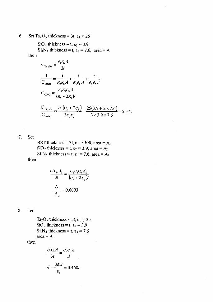
6. Set Th2O5 thickness : 3t, e1:25
SiOz thickness : t, ez: 3.9SLN+ thickness : t, E3:7.6, area: A
then
c T o r o r :
I
qqA3t
t= _ + _ + _Co*o Er€oA ereoA er4A
co*o=ffi,
Ct" ro , -e r (e r+Zer )Co*o 3Er€,
_ z s ? . g + z x t . a ) = 5 . 3 7 .3x3 .9 x7 .6
7. Set
8. Let
TazOs thickness :3t" e1 :25SiOz thickness : t, e2: 3.9Si:Nq thickness : t, 4:7.6area: A
then
qqA _4€oA
d =3 t ' t =0 .46g t .q
then
BST thickness : 3t, e1 : 500, area : 41SiOz thickness : t, a2:3.9, area: AzSi:Na thickness : t, E3:7.6, area: Az
o' = o.oonr.A2
444, =3t

9. The deposition rate can be expressed as
r: ro exp (-E^/kT)
where E": 0.6 eV for silane-oxygen reaction. Therefore for Tt : 698 K
r(r,) =2=€XDlo.{ L_ t ) I4 r , )
' L ( k 4 k r , ) )
, 'z : 06 [ f ry_3oo] Io.o2s9 L\6e8 r, ) )
_ Tz:1030 K: 757
We can use energy-enhanced CVD methods such as using a focused energy
source or UV lamp. Another method is to use boron doped P-glass which will
reflow at temperatures less than 900 .
I 1. Moderately low temperatures are usually used for polysilicon deposition, and
silane decomposition occurs at lower temperatures than that for chloride
reactions. In addition, silane is used for better coverage over amorphous
materials such SiO-,.
12. There are two reasons. One is to minimize the thermal budget of the wafer,
reducing dopant diffusion and material degradation. In addition, fewer gas
phase reactions occur at lower temperatures, resulting in smoother and better
adhering filrns. Another reason is that the polysilicon will have small grains. The
finer grains are easier to mask and etch to give smooth and uniform edges.
However, for temperatures less than 575 "C the deposition rate is too low.
13. The flat-band voltase shift is
L V F B D [ l ! [ [ QO,
co
10.
c^ =to ' - 3 '9x 8 '85 x lo- 'a =6.9 x l0* F/cm-r I" d 5 0 0 x 1 0 - o
- Number of fixed oxide charse is

0.5C, _ 0.5 x 6.9 x l0-8 =2.1x l0r , cm-,q 1 .6 x 10 - ' '
To remove these charges, a 450 heat treatment in hydrogen for about 30
minutes is required.
14. 20/0.25: 80 sqs.
Therefore, the resistance of the metal line is
5 x 5 0 : 4 0 0 O .
15. For TiSiz
3 0 x 2 . 3 7 : 7 l . l n mFor CoSio
30 x 3.56: 106.8nm.
16. For TiSiz:
Advantage: lowresistivity
lt can reduce native-oxide layers
TiSiu on the gate electrode is more resistant to high-field-
induced hot-electron degradation.
Disadvantage: bridging effect occurs.
Larger Si consumption during formation of TiSiu
Less thermal stabilifv
For CoSb:
Advantage: lowresistivity
High temperature stability
No bridging effect
A selective chemical etch exits
Low shear forces
Disadvantage: not a good candidate for polycides

1 7 . ( a ) O = e + = 2 . 6 7 x t 0 6 x = 3 . 2 x 1 0 3 Q0 . 2 8 x 1 0 - a x 0 . 3 x l 0 - a
tA eTL
d s3 . 9 x 8 . 8 5 x l 0 - r a x 0 . 3 x 1 0 + x l x l 0 a x 1 0 - 6
0 .36 x l 0 -a
RC =3 .2x105 x2 .9x l } - t s =0 .93ns
(b) R= p+=r .7 x10-6 x - .=+ = 2 x I 0 3 C )A 0.28 x 10-a x 0.3 x 10r
= 2.9 x l0 -r '
F-
€A {L 2.8 x 8.85 x l0- 'o x 0.3 x 10-a x 1( _ = - = - : -d s 0.36 x l0-o
2 ' I x 10- '3 F
RC =2 x 10 t x 2 .1x l 0 - ' 3 =0 .42ns
o 4 )(c) We can decrease the RC delay by 55%. Ratio :
,r; :0.45.
18. (a) R = eL=2.67x l0* = 3.2 x l0 'C)' A 0 . 2 8 x l O o x 0 . 3 x l 0 o
C = 4 = { L - 3 . 9 x 8 . 8 5 x 1 0 - ' a x 0 . 3 x 1 0 { x l x 3 = g . 7 x l 0 - , r Fd .S 0.36 x l0o
RC : 3.2 x 103 x8.7 x 10-13 : 2.8 ns.
T 1( b ) R = O : = l . 7 x 1 0 - 6 x 4 = 2 x l 0 r C )' A
0 . 2 8 x l 0 o x 0 . 3 x l O o
a 4 { L 2 . 8 x 8 . 8 5 x 1 0 - ' o x 0 . 3 x l 0 { x l x 3d s 0.36 x 10a
= 6 '3 x l0- t3 F
R C = 2 x 1 0 3 x 8 . 7 x 1 0 - t 3 = 2 . 5 n s
RC =3.2 x 103 x 8.7 x l0- '3 = 2.5 ns.
19. (a) The aluminum runner can be considered as two segments connected in series:
20%o (or 0.4 mm) of the length is half thickness (0.5 pm) and the remaining
1.6 mm is full thickness (lpm). The total resistance is
*=JL . ! "1=g* ro -u f 9 ' 16 , * , o ' oo - l' l A , A r ) [ 1 0 - * x l 0 - * l 0 - o x ( 0 . 5 x 1 0 - ' ) l
: 7 2 U .

20.
The limiting current 1 is given by the maximum allowed current density times
cross-sectional area ofthe thinner conductor sections:
. / : 5x10s Ncr*" (10-ax0.5x10-a; : 25x103 A:2.5 mA.
The voltage drop across the whole conductor is then
V: N =72Qx2 .5x l 0 - ' A :0 .18V .
40 nm
60 nm
h:height, W;width, r: thickness, assumethatthe resistivities of the cladding
layer and TiN are much larger than p n, and pru
R , , = D , , * (
= 2 . 7 Ih xW (0.5 - 0 .1) x 0.5
R. . . = p, . . , -J- =1.7 (
hxtr (0.5 - 2t) x(0.5 -2t)
When Rn, = Rru
2 . 7 1 . 7l n e n = -
0.4 x 0.5 (0.5 -2t)'�
= t : 0 .073 pm: 73 nm .
0.5 pm

CHAPTER 12
I . With reference to Fig.2 for class 100 clean room we have a total of 3500 particlesinf withparticle sizes >0.5 pm
2L t 3596: 735 particles/r# with particle sizes > 1.0 pm100
** 35OO: 157 particles/# with particle sizes > 2.0 1tmr00Therefore, (a) 3500-73 5 : 2765 particles/nf between 0.5 and I pm
(b\ 735-157 :578 particles/m3 befween 1 and 2 pm(c) 157 particles/# above 2 pm.
:. y = fr,r-o,n
A :50 mm2:0.5 cm2l r _ e4(0 . rx0 .s ) * "4 (o2sxo.s ) * " - t { txo .s ; =g- r .z =30. lyo .
I The available exposure energy in an hour is0.3 mW2/cmz x 3600 s:1080 mJlcr*
For positive resist, the throughput is1080_ = 7 wafers/ty140
For negative resist, the throughput isloSo - 120 wafervtrr.
9
1. (a) The resolution of a projection system is given byL 9.6,1 9:193fgt = o.r7g pmt^ =Kt f r f .=u 'u ̂
0 .65
DoF = k,-L= o.sl o,le,3f l: o.r28 u*'(NA)'� L (0.65)'� I
(b) We can increase NA to improve the resolution. We can adopt resolution enhancement
techniques (RET) such as optical proximity correction (OPC) and phase-shifting Masks
(PSM). We can also develop new resists that provide lower h and higher k2 for better
resolution and depth of focus.
(c) PSM technique changes kr to improve resolution.
j. (a) Using resists with high y value can result in a more vertical profile but tkoughput
decreases.
(b) Conventional resists can not be used in deep UV lithography process because these resists
have high absorption and require high dose to be exposed in deep [fV. This raises the

6. (a)
7. (a)
( b )
(c)
(b)
8 .
9.
concern of damage to stepper lens, lower exposure speed and reduced throughput.
A shaped beam system enables the size and shape of the beam to be varied, thereby
minimizing the number of flashes required for exposing a given area to be patterned.
Therefore, a shaped beam can save time and increase throughput compared to a Gaussian
beam.
We can make alignment marks on wafers using e-beam and etch the exposed marks. We can
then use them to do alignment with e-beam radiation and obtain the signal from these marks
for wafer alignment.
X-ray lithography is a proximity printing lithography. lts accuracy requirement is very high,
therefore alignment is difficult.
X-ray lithography using synchrotron radiation has a high exposure flux so X-ray has better
throughput than e-beam.
To avoid the mask damage problem associated with shadow printing, projection printing
exposure tools have been developed to project an image from the mask. With a 1:l
projection printing system is much more difficult to produce defect-free masks than it is
with a 5:l reduction step-and-repeat system.
It is not possible. The main reason is that X-rays cannot be focused by an optical lens.
When it is through the reticle. So we can not build a step-and-scan X-ray lithography
system.
As shown in the figure, the profile for each case is a segment of a circle with origin at the
initial mask-film edge. As overetching proceeds the radius of curvature increases so that
the profile tends to a vertical line.
(a) 20 sec
0.6 x 20/60:0.2 pm....(100) plane
0.6/16 x 20/60 : 0.0125 pm.... . . . .( l l0) plane
0.6/100 x 20/60: 0.002 pm.... . . .(t I 1) plane
wo = wo - .l-zt = 1.5 - "li x0.z = 1.22 pm
40 sec(b )
0.6 x 40/60:0.4 pm....(100)plane

0.6/16 x 40/60 : 0.025 pm.... ( l t0) ptane
0.6/100 x 40/60: 0.004 pm.... .( l I l) plane
wu =wo -Jzt = 1.5- Ji xo.a:0.93 pm
(c) 60 sec
0.6 x l :0 .6 pm.. . . (100)p lane
0.6/16 xl: 0.0375 pm.... ( l l0) plane
0.6/100 x l: 0.006 pm.....(l I l) plane
W o : W o - J z t = 1 . 5 - J 2 x 0 . 6 : 0 . 6 5 p m .
[-sing the data in Prob. 9, the etched pattem profiles on <100>-Si are shown in below.
(a t 20 sec I :0112 ltm, Wo = Wu = 1.5 pm
(b r -10 sec l:0.025 ltm, Wo - l[t = 1.5 pm
(ct60 sec l :0 .0375 1tm Wo -Wu = 1.5 pm.
lf u'e protect the IC chip areas (e.g. with SfNa layer) and etch the wafer from the top, theri idth of the bottom surface is
r r ' = tTt + Jzt = 1000 *JT*625 = 1884 pm
l-he fraction of surface area that is lost is
(r ' ' - t4/:)/w2 x 100%:(1g842-10002) /t8842x 100%:71.8%
In terms of the wafer area. we have lost
7 1.8 % x tdl5 / 2)' :127 cr*
Another method is to define masking areas on the backside and etch from the back. The widthtrf each square mask centered with respect of IC chip is given by
v [ =Wr -^ l - z t=1000- J i x625 :116 pm
[- sing this method, the fraction of the top surface area that is lost can be negligibly small.
I Pa: 7 .52mTon

PV: NRT
7.52 /760, 10-3 : n/V x0.082 x 273
n/V: 4.42 x l0-7 mole/liter:4.42 x l0-7 x 6.02 " 1023/1000 :2-7 ,l}ta cm3
mean-free-path
2,= 5xI0-3 /P cm:5x l0-3 x1000/ 7.52:0.6649 cm:6649 pm
l50Pa: ll28 m Torr
PV nRT

ll28l 760 x 10-' : n/V x 0.082 x 273
n/V : 6.63 x 10-s mole/liter : 6.63 x lQ-sxg.Q/x 1023/1000 :-4 x 10¹⁶ crn3
mean-free-path
2": 5 xl}- ' /Pcm : 5* 10-3 x1000/1128 : 0.0044 cm : 44 um.
l-1. Si Etch Rate (nm/min) :2.86 x 10⁻¹³ x n, x7/' ,r-tiA'
:2 .86x l0 - r3 x lx lSrsx(2 9 t1 / , , r#
:224.7 nm/min.
11. SiOz Etch Rate (nm/min): Q.Sl{x 10-13 *3" Iytsx(2Oq% ^"#: 5.6 nm/min
Etch selectivity of SiOz over Si : #=
0.025
or etch rate (Sio2)/etch rate (Si) : ':u-)!
""t-t'u*'ot/n'7x2e8 - 0.025 .' 2 .86
15. A three-step process is required for polysilicon gate etching. Step 1 is a nonselective etch
process that is used to remove any native oxide on the polysilicon surface. Step 2 is a high
polysilicon etch rate process which etches polysilicon with an anisotropic etch profile. Step 3 is
a highly selective polysilicon to oxide process which usually has a low polysilicon etch rate.
I 6. If the etch rate can be conholled to within l0 %o, the polysilicon may be etched 10 o/o longer or
for an equivalent thickness of 40 nm. The selectivity is therefore
40 nm/l nm:40.
17. Assuming a30Yo overetching, and that the selectivity of Al over the photoresist maintains 3.
The minimum photoresist thickness required is

t 8 .
( l+ 30%) x I pm/3 :0.433 pm:433.3 nm.
qB( I ) " =-
me
2nx2.45 x 10e =[ . 6 x 1 0 - ' e x B
9 . l x 1 0 - 3 1
B: 8.75 x 10⁻²(tesla)
:875 (gauss).
Traditional RIE generates low-density plasma (10e crn3) with high ion energy. ECR and ICp
generate high-density plasma (10rr to 1012 crn3) with low ion energy. Advantages of ECR and
ICP are low etch damage, low microloading, low aspect-ratio dependent etching effect, and
simple chemistry. However, ECR and ICP systems are more complicated than traditional RIE
systems.
The corrosion reaction requires the presence of moisture to proceed. Therefore, the first line of
defense in controlling corrosion is controlling humidity. Low humidity is essentiaf. especially
if copper containing alloys are being etched. Second is to remove as much chlorine as possible
from the wafers before the wafers are exposed to air. Finally, gases such as CF+ and SF6 can be
used for fluorine/chlorine exchange reactions and polymeric encapsulation. Thus, Al-Cl bonds
are replaced by Al-F bonds. Whereas Al-Cl bonds will react with ambient moisture and start
the corrosion process , Al-F bonds are very stable and do not react. Furthermore, fluorine will
not catzlyze any corrosion reactions.
l 9
I (J .

l. E"(boron) :3.46 eV, D :0.76 cn?/sec
From Eq. 6,
CHAPTER 13
4.142xl0-" x 1800 = 2.73x10a cm
-3 .46
8.614x l}-s x1323
- F o . le r *o(
-3 '46D = D o e x ? ( # ) = .
t g . 6 t 4 x l o _ 5x1223)=o ' t+zx 1o-"cm' ls
L=JDt =
From Eq. 9, c (x) = c,ertu (fi)= 1.8 x I 02oerfc (17{6;)
I f x =0 ,C(0)= 1 .8x1020 a ioms /cm3;x :0 .05 t104,C(5* 105) :3 .6 x l0 le
atoms/cm3; x : 0.07 5 r I 0-4, C(7.5 x 1 0-6 ) : g.4 x 1 gls atoms/c rrf ;, :0. I " I 0-a,
C(10-s): 1.8 x l0r8 atoms/cm3;
x :0 .15x 104, C1 l .5x l0 -5) : l .gx l016 a toms/c# .
The x., =ZJDI (efc 'gs!-- ) =o.l5Arn
Total amount of dopant introduced : Q(0
1:#C,L = 5.54x lOtaatoms/c#.
4n
2 ' D=Do*(#)=oz6exn()=
o ' 'ux1o- 'ocm'/s
From Eq. 15, Cs = C(Q,t)= + =2.342x 10'natomVcm 3Jtilt
C(x\ =C-"rf. [a) =2.342*to'nerrc[ " )"
\ 2L ) \ 2 .673x r0 - ' )
I fx :0, C(0): 2.342 x 10le atoms/crrf ;*:0. lxl0-a, C(l0r) : l .4lxl0te atoms/cm3;
x : 0.2x10⁴, C12xl0't) : 6.7911018 atoms/c nf ; * :0.3 x l6-a, C(3 x lo-5; : 2.65 x 10t8

3 . 1 x 1 0 " = t * t O " " * p [
t : 1573 s:26 min
atoms/cm';
x :0.4x10⁴, c14x10-s; : 9 .37x10t7 atoms/cm3;x :0 .5x10-4, c15xlO-s) : 1 .g7x1gtz
atoms/cm3;
x : 0.6x10⁴, c(6x 10-t) : 3.51* 1016 atoms/crrt; t :0.7x10-a, c(7x l0-5) : 7.03x l0r5
atoms/cm3;
.r :0.8x10⁴, C(8x10-s) :5.62x101a atoms/cm3.
The x, = 4Dtht - - = 0.72qm.C uJ tDr
l0- ' )4x2 .3x10 ' ' t )
For the constant-total-dopant diffusion case, Eq. 15 gives C, = -L*Dt
s = 1 x lottm = 3.4xlo*atomVcm t.
4. The process is called the ramping of a diffusion fumace. For the ramp-down situation, the
furnace temperature T is given by
T : T o - r t
where To is the initial temperature and r is the linear ramp rate. The effective Dt product
during a ramp-down time of tr is given by
(Dt)"r = l^' ogyat
In a typical diffirsion process, ramping is carried out until the diffirsivity is
negligibly small. Thus the upper limit t1 con be taken as infinity:
l l l r t- = - * ( l + - + . . . )T T - r t T ' T
0 0 0

and
( - n / \ - l - r r t . l - E - , . - r E t - r E tD=Do exp[ " hr l=Do "*pl 1+A*;* . . . ) l :Oo("*p 3"_ Xexp-#. . . )= D(T;"ry#
\ / r u r / L k I o I o J k l o k f o -
\ u / T k T ^ ,
where D(To) is the diffusion coefficient at T6. Substituting the above equation into the
expression for the effective Dr product gives
(Dt)"n = [i otr,\"*p-]#dt = D(r)+' k T o '
' " ' ' E o
Thus the ramp-down process results in an effbctive additional time equal to Kls2/rgu at
the initial diffi.rsion temperature T6.
For phosphorus difflrsion in silicon at 1000"C, we have from Fig. 4:
|{7d : D (1273 K) : Zx 10-ra cm2ls
1273 -773r = - = 0 . 4 1 7 K / s
20x 60
E" :3 .66 eY
Therefore, the effective diffusion time for the ramp-down process is
oro' _. l.3g xlo-r'(1273)'
= 9ls = 1.5min .,Eo 0.417(3.66x 1.6 x 10- 'n)
5. For low-concentration drive-in diffusion, the diffusion is given by Gaussian distribution.
The surface concentration is then
, s , s ( r " \C(0.t) =+=---exDl -i i
4d)t Jil; ' \2kr)
{ = _L.,*l,&Y-r"' ) = _0.5 *gdt .|1il,
' \2ftrl( 2 ) t

dC dt= - 0 . 5 x -
C t
which means lYo change in diffusion time will induce 0.5Yo change in surface
concentration.
d c , s ( E - \ ( - E - ) E _- - - - : ' s . v r - [ -
dT Jri lo, '
\zkr )\2kT'� ) zkT'
dc - E dT - 3.6 x 1.6 x lo- ' ' dT dTnr , . . . . . . . . . . . . . ._ - a 1L i . .
C 2 k T T 2 x l . 3 8 x l 0 - " x 1 2 7 3 T T
which means lo/o change in diffirsion temperature will cause 16.9% change in
surface concentration.
6. At I 100oC, ni : 6x 10¹⁸ crn3. Therefore, the doping profile for a surface concentration
of 4 x 10¹⁸ crn3 is given by the "intrinsic" diffi.rsion process:
c(x.t)= c"..r"[4]\2''lDt )
where C, : {x 1018 crn3, t: 3 hr: 10800 s, and D : 5x10⁻¹a cm2ls. The
diffusion length is then
J Dt = 2.32x10⁻⁵ cm = 0.232 tm
The distribution of arsenic is C(x) = 4 x 10¹⁸ "rf"[---:-)[4.64 xl0-' )
The junction depth can be obtained as follows
10"=4x l0" " . f r f t '
- l( 4.64 x 10- ' J
xi: I.2x 104 cm : 1.2 pm.
7. At 900oC, ni:2x 10¹⁸ crn3. For a surface concentration of 4x10tt "-', given by

the "extrinsic" diffusion process
8 .
x t =1.6J Dt = 1.6m = 3.23x l0*ucm = 32.3 nm .
lntrinsic diffusion is for dopant concentration lower than the intrinsic carrier
concentration ni at the diffusion temperature. Extrinsic diffi.rsion is for dopant
concentration higher than n;.
9. For impurity in the oxidation process of silicon,
segregatio ncoefficein t =
3 x 1 0 " 3f=-- - . . -=- : -=0.006.
5 x 10 ' ' 500
[0.5: [1 .1 + qFp/Ci
-E , -4 .05x1.6x10- le
D = D o e k r x "
= 4 5 . 8 e t 3 8 " 1 0 2 r * r l ? l
ni
r ' - € " -" * -Z
, , -3 '45x lo r xo .6 = 1 .3 x lo ,cm- '" I .6 x l0 - ' "
10-t; t = 1 . 3 x 1 0 ' t x l . 6 x l 0 - t n
i4r0.16)'
the implant time r :6.7 s.
12. The ion dose per unit area is
" l# =3.77x10- 'ucm2ls
10 .
1 1 .
3 . 9 x 8 . 8 5 x 1 0 - r a= 3 . 4 5 x 1 0 - 710-u
f t 1 0 x 1 0 { x 5 x 6 0N = q = l .6x lQ- te =2 .3gx1012 ions /cm2A A , I 0 . ,n "\T)-
From Eq. 25 and Example 3, the peak ion concentration
indicates the oo is 20 nm.
is at x : Ro. Figure. l7

Therefore, the ion concentration is
^9 2.38 x 10' ' �= -___-___-___-_ :. = 4.74 x l0'tCm
-3 .
oo42n 20x10- ' 42 t r
13. From Fig. 17,the &:230 nm, and oo = 62 nm.
The peak concentration is
S 2 x 1 0 ' 5: ---------------- = l.29x l0'ocm-loo {2 t t 62x10- ' 42n
From Eq. 25,
t.2ex,o" "*[3:i{l| 260- J
x; :0 .53 pm.
14. Dose per unit area : 9 =CoLVr - 3'9 x8'85 x 10*ta xlq q 250 x 10-s x l -6 x 10- 'n
= 8 '6 x10"cm-2
From Fig. 17 and Example 3, the peak concentration occurs at 140 nm from the
surface. Also, it is at (140-25): 115 nm from the Si-SiOz interface.
15. The total implanted dose is integrated from Eq. 25
e,= f s-"*[-t*I{ l*=l{r*fr- errcl Re-,- l}=lo -erfc(z. 'sur - lo
@- | 2oo. J z I L o,. lz l) z- 3)l= r-xt 'ee8e
The total dose in silicon is as follows (d:25 nm):
Q,,=I:; fu"*|#]*=i{ ' - [ '_", f"(* i , ]}=; ' -er|c(| .87)]={xl.99l8
the ratio of dose in the silicon: Qs/Qr:99.6%.

16. The projected range is 150 nm (see Fig. 17).
The average nuclear energy loss over the range is 60 eV/nm (Fig. 16).
60x 0.25: 15 eV (energy loss of boron ion per each lattice plane)
the damage volume: Vo: n (2.5 nm;21tSO nm):3" 10-18 cm3
total damage layer : 150/0.25: 600
displaced atom for one layer: l5l15 : I
damage densitY : 600/Vo : 2" l02o cm3
zxlo2o / 5.02x10² : 0.4%.
17. The higher the temperature, the faster defects anneal out. Also, the solubility of
electrically active dopant atoms increases with temperature.
o1 8 . L V , = l V : = ''
Cor
where p1 is the additional charge added just below the oxide-semiconductorsurface by ion implantation. Cox is a parallel-plate capacitance per unit area
given by C"" =1a
(d is the oxide thickness, €r is the permittivity of the semiconductor)
e, = LV,c". - 1v x 3'9 x 8'85 x 10-'4F/cm : g.63x r0-' c;
0.4 x l0 -6cm cm'
8'63 x 1o-' : 5.4 x1ol2 ions/c#1.6 x 10- te
Total implant dose: t'0,\!9" :1.2 x 10¹³ ions/c#.
45%
19. The discussion should mention much of Section 13.6. Diffi.rsion from a surface film
avoids problems of channeling. Tilted beams cannot be used because of
shadowing problems. If low energy implantation is used, perhaps with
preamorphization by silicon, then to keep the junctions shallow, RTA is also
necessary.
20. From Eq.35
& = 1 "rp"[o o-g)= 0.84^ s 2 [ 0 . 2 J 2 )
The effectiveness of the photoresist mask is only 16%o.
s, = l.rr"ig) =0.023.s 2 \0.2J2 )
The effectiveness of the photoresist mask is 97.7%.
2 1 . r = ] - { u - � l o - ,24n u
. ' . u = 3 . 0 2
d: &+ 4.27 op: 0.53 + 4.27 x 0.093 = 0.927 pm.

CIIAPTER 14
l. Each U-shape section (refer to the figure) has an area of 2500 pm x 8 pfft:2 x
10a pm2. Therefore, there are (250(|)2/2*104:312.5 U-shaped section. Each
section contains 2long lines with 1248 squares each, 4 corner squares, 1 bottom
square, and 2 halfsquares at the top. Therefore the resistance for each section is
l kO/i l (1248x2 +4x0.65 +2):2599.6 kO
The maximum resistance is then
3r2.5x2500.6:7.8t * 108 C) : 781 MO
2.5 mm
2. The area required on the chip is
, c o ( 3 0 x l o - ' X 5 x l 0 - , , )Eo, 3.9 x 8.85 x l0-tu
= 4.35x 10⁻⁵ cm2
4Pm(PITCH)
:4 .35 " 103 pmz :66 x 66 pm

Refer to Fig.4a and using negative photoresist of all levels
(a) Ion implantation mask (for p+ implantation and gate oxide)
(b)Contact windows (2x10 pm)
(c) Metallization mask (using Al to form ohmic contact in the contact window
and form the MOS capacitor).
Because of the registration errors, an additional2 pm is incorporated in all critical
dimensions.

( o )
56 pm
I
II
{ l + 2 F m
Zli* ( b )
1
73
If the space between lines is 2 p*, then there is 4 pm for each turn (i.e., 2xn, for
one tum). Assume there are n turns, from 8q.6, [, x 1tan2r * 1.2 x 10-6r?r, where r
can be replaced by 2 x n. Then, we can obtain that n is 13.

4. (a) Metal 1, (b) contact hole, (c) Metal2.
(a) Metal l,
(b) contact hole,
I(c) Metal2.
I

5. The circuit diagram and device cross-section of a clamped transistor are shown in
(a) and (b), respectively.
COLLECTOR E M I T T E R
Si02
(a) The undoped polysilicon is used for isolation.
(b) The polysilicon I is used as a solid-phase diffusion source to form the
extrinsic base region and the base electrode.
(c) The polysilicon 2 is used as a solid-phase diffusion source to form the emiffer region
and the emitter electrode.
(a) For 30 keV boron, & : 100 nm and A,Ro: 34 nm. Assuming that .Ro and A,Ro
for boron are the same in Si and SiOz the peak concentration is given by
( o )
( b )
6 .
7.
P -SUBSTRATEoHilrcCONTACT
J-zntn,J:19f- =9.4xro,u cm-,t l2nQa x l0- ')

The amount of boron ions in the silicon is
f;=rffiq"*lWs [ ( n " -d . t l
==12 _ erf ,c l _+_ l l2L [^/2m,.,1-18 x l o " [ ^ ^ ( 7 5 0 ) l
= - t z - E l t v t - = : - I I2 L \ Jz *340 ) l
= 7.88 x 10"cm- '
Assume that the implanted boron ions form a negative sheet charge near the Si-
SiO2 interface, then
LVr = re)/ Co, =-J:6 1 10-'' x (7'88 x 10" )' l q ) 3 .e *8 .8m=o 'e l v
(b) For 80 keV arsenic implantation , &:49 nm and A & : 1S nm. The peak arsenic
concentration i, J- - - 10'u = 2.21x 10², cm-, .42nA,R" r /ax( l8x l0- ' )

Rp =49oi (As)
tu;\\
\.o"r.*.
\
\
\
\
\
IBORON \
(LOWER ScaLsl 1
/ar\
Re-toooi (B)
I{ol5o d tooo -zm
-tso.r-zsoix(i) - FoR cHAls{EL Rectfi
8. (a) Because (100)-oriented silicon has lower (- one tenth) interface-trapped charge and
a lower fixed oxide charge.
(b) If the field oxide is too thin, it may not provide a large enough threshold
voltage for adequate isolation befween neighboring MOSFETs.
(c) The typical sheet resistance of heavily doped polysilicon gate is 20 to
30 Q fl, which is adequate for MOSFETs with gate lengths larger than 3 pm. For
shorter gates, the sheet resistance of polysilicon is too high and will cause large
RC delays. We can use refractory metals (e.g., Mo) or silicides as the gate
material to reduce the sheet resistance to about I O /t1.

(d) A self-aligned gate can be obtained by first defining the MOS gate structure, then
using the gate electrode as a mask for the source/drain implantation. The self-
aligned gate can minimize parasitic capacitance caused by the source/drain
regions extending underneath the gate electrode (due to diffusion or
misalignment).
(e) P-glass can be used for insulation between conducting layers, for diffi.rsion and
ion implantation masks, and for passivation to protect devices from impurities,
moisfure, and scratches.
9. The lower insulator has a dielectric constant Alq: 4 and a thickness dr l0 nm The
upper insulator has a dielectric constant A/q : 10 and a thickness dz: 100 nm. Upon
application of a positive voltage Vc to the extemal gate, electric field E 1 and E2 arc
established inthe dt and dz respectively. We have, from Gauss' law, that e1E1: e2E2
+Q and Vc: Erdt *Ezdz
where Q is the stored charge on the floating gate. From these above two equations, we
obtain
" - v o - Q-l d, + d,(q ltr)
' g * er(a, tar)
a
I
r - , ^ - , I l o x l o ? O' | | 4 \ | / r ^ t , l
Iro+roolrJ f . ' tff iJ],.r.rsx ro-'o
If the stored charge does not reduce E1 by a significant amount (i.e.,0.2>> 2.26x10s
lQ l, *" can write
Q = foadf
x 0.2 Lt = o.z x (o.zsx tO-u)= 5 x t0-s C
L V - : Q = , 5 x l o - 8' c2 ( lo*8.s@=o'565
v
(a)

10.
(b) when t -) a,J -+}we have lgl-+ 0.212.26x10s = 8.84x10⁻⁷ C.
8.84x l0 -?Then L,Vr=t=, ( t0x8 .85 x 1g- t4 )716-5
=9.98 V.
(o) p-TUB
(b) POLYSILICOT{ GATE
(c) n-TYPE O|FFUSION
+ +
+ +
+ +
+ +

+
{d) p-TypE DtFFUstoN
++
t r n
t r n(e) CONTACT WINDows
+
(f) METALLTZATIOTTI
11. The oxide capacitance per unit area is given by
€"rn
C ̂ - = ' '7 = 3.5 x l0 t F/cm2d
and the maximum current supplied by the device is
r " , = ! \ rc, ,(vo -v,) ' =: :+3.5xt0r (vo -v,) '= 5 mA2 L - 2 0 . 5 t t n

and the maximum allowable wire resistance is 0.1 V/5 mA. or 20Q. Then. the
length of the wire must be
- Rx Area 20O x I0 - tcm't - _ = 0.074 cm
p 2 .7 x l } 'Q - cm
or 740 pm. This is a long distance compared to most device spacing. When
driving signals between widely spaced logic blocks however, minimum feature
sized lines would not be appropriate.
12.

s i 3N4x x
I ll,*fv - EPITAXY
FIELD OXIDE
( b l
( o )
( d )
( e )
i tap*
RESIST
1 3 .
14.
To solve the short-channel effect ofdevices.
The device performance will be degraded from the boron penetration. There are
methods to reduce this effect: (1) using rapid thermal annealing to reduce the
time at high temperatures, consequently reduces the diffusion of boron, (2) using
nitrided oxide to suppress the boron penetration, since boron can easily combine
with nitrogen and becomes less mobile, (3) making a multi-layer of polysilicon
to trap the boron atoms at the interface of each layer.
Total capacitance of the stacked gate structure is :15 .
c _q "z l(z.e-)d, d, l \d , d , )
7 2 s / ( 7 2 5 \= - x - / l - + - l : 2 . 1 2
0.s l0 l \0 .5 to )
16.
3 ' 9 = 2 . 1 2d
. ' . d = 3'9 =1.84 nm.2 . 1 2
Disadvantages of LOCOS: (1) high temperature and long oxidation time cause V1
shift, (2) bird's beak, (3) not a planar surface, (4) exhibits oxide thinning effect.
Advantages of shallow trench isolation: (l) planar surface, (2) no high
temperature processing and long oxidation time, (3) no oxide thinning effect, (4)
no bird's beak.
For isolation between the metal and the substrate.
GaAs lacks of high-quality insulating film.
t7 .
1 8 .

19. (a)
: 2000 * (el.o: x l0- 'o )= 1.38 x 10-'s = 1.38 ns.
(b) For a polysilicon runner
( r . \ ( l )RC = | R,ouo,"# ll t",- |
\ w ) \ d )( t \ ,
= 391 -- l- l(ol.or>< t0-'o) =2.07 xl0-7 s\ 1 0 - " , / '
= 2 0 7 n s
Therefore the polysilicon runner's RC time constant is 150 times larger than the
aluminum runner.
20. When we combine the logic circuits and memory on the chip, we need multiple
supply volrages. For reliability issue, different oxide thicknesses are needed for
different supply voltages.
21' (a) /r^^, = /cr^,o,
* /r,u,,o"
hence uo%'='%r* 1% =fi 3 A
(b) Eor : 16.7 A.