rx23t group datasheet - renesas electronics
TRANSCRIPT
Datasheet
R01DS0248EJ0110 Rev.1.10 Page 1 of 98Jan 13, 2016
RX23T GroupRenesas MCUs
Features 32-bit RX CPU core Max. operating frequency: 40 MHz
Capable of 65.6 DMIPS in operation at 40 MHz Enhanced DSP: 32-bit multiply-accumulate and 16-bit
multiply-subtract instructions supported Built-in FPU: 32-bit single-precision floating point
(compliant to IEEE754) Divider (fastest instruction execution takes two CPU clock
cycles) Fast interrupt CISC Harvard architecture with 5-stage pipeline Variable-length instructions, ultra-compact code On-chip debugging circuit Memory protection unit (MPU) supported
Low power design and architecture Operation from a single 2.7-V to 5.5-V supply Three low power consumption modes
On-chip code flash memory, no wait states 128-/64-Kbyte capacities On-board or off-board user programming
On-chip SRAM, no wait states 12 Kbytes of SRAM
DMA DTC: Four transfer modes
Reset and supply management Seven types of reset, including the power-on reset (POR) Low voltage detection (LVD) with voltage settings
Clock functions Main clock oscillator frequency: 1 to 20 MHz External clock input frequency: Up to 20 MHz PLL circuit input: 4 MHz to 12.5 MHz On-chip low-speed oscillator, on-chip high-speed
oscillator, dedicated on-chip oscillator for the IWDT Clock frequency accuracy measurement circuit (CAC)
Independent watchdog timer 15-kHz on-chip oscillator produces a dedicated clock
signal to drive IWDT operation.
Useful functions for IEC60730 compliance Self-diagnostic and disconnection-detection assistance
functions for the A/D converter, clock frequency accuracy measurement circuit, independent watchdog timer, RAM test assistance functions using the DOC, etc.
MPC Multiple locations are selectable for I/O pins of peripheral
functions
Up to 4 communications channels SCI with many useful functions (2 channels)
Asynchronous mode, clock synchronous mode, smart card interface mode, simplified SPI, simplified I2C, and extended serial mode.
I2C bus interface: Transfer at up to 400 kbps (one channel) RSPI capable of high speed connection (one channel)
Up to 12 extended-function timers 16-bit MTU3: 40MHz operation, input capture, output
compare, three-phase complementary PWM output, CPU-efficient complementary PWM, phase counting mode (six channels)
8-bit TMRs (4 channels), 16-bit compare-match timers (4 channels)
12-bit A/D converter: 10ch On-chip sample-and-hold circuit: 12bit × up to 3 channels Sampling time can be set for each channel Self-diagnostic function and analog input disconnection
detection assistance function (compliant to IEC60730) ADC: three sample-and-hold circuits, double data
registers, comparator (3 channels)
Register write protection function can protect values in important registers against overwriting.
Up to 50 pins for general I/O ports 5-V tolerant, open drain, input pull-up
Operating temperature range 40 to +85C 40 to +105C
Applications General industrial and consumer equipment
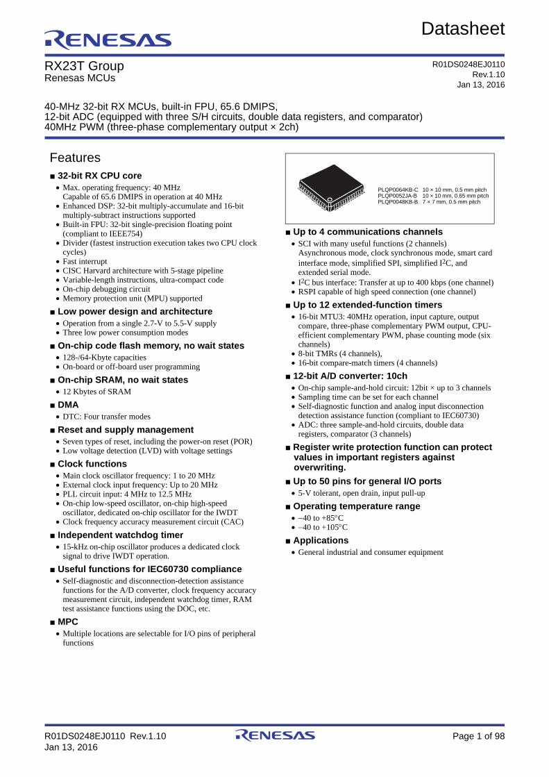
PLQP0064KB-C 10 × 10 mm, 0.5 mm pitchPLQP0052JA-B 10 × 10 mm, 0.65 mm pitchPLQP0048KB-B 7 × 7 mm, 0.5 mm pitch
40-MHz 32-bit RX MCUs, built-in FPU, 65.6 DMIPS, 12-bit ADC (equipped with three S/H circuits, double data registers, and comparator)40MHz PWM (three-phase complementary output × 2ch)
R01DS0248EJ0110Rev.1.10
Jan 13, 2016

R01DS0248EJ0110 Rev.1.10 Page 2 of 98Jan 13, 2016
RX23T Group 1. Overview
1. Overview
1.1 Outline of Specifications
Table 1.1 lists the specifications, and Table 1.2 gives a comparison of the functions of the products in different
packages.
Table 1.1 is for products with the greatest number of functions, so the number of peripheral modules and channels will
differ in accordance with the package type. For details, see Table 1.2, Comparison of Functions for Different
Packages.
Table 1.1 Outline of Specifications (1/3)
Classification Module/Function Description
CPU CPU Maximum operating frequency: 40 MHz 32-bit RX CPU (RX v2) Minimum instruction execution time: One instruction per clock cycle Address space: 4-Gbyte linear Register set
General purpose: Sixteen 32-bit registersControl: Ten 32-bit registersAccumulator: Two 72-bit registers
Basic instructions: 75 Variable-length instruction format Floating-point instructions: 11 DSP instructions: 23 Addressing modes: 11 Data arrangement
Instructions: Little endianData: Selectable as little endian or big endian
On-chip 32-bit multiplier: 32-bit × 32-bit → 64-bit On-chip divider: 32-bit ÷ 32-bit → 32 bits Barrel shifter: 32 bits Memory protection unit (MPU)
FPU Single precision (32-bit) floating point Data types and floating-point exceptions in conformance with the IEEE754 standard
Memory ROM Capacity: 64 K/128 Kbytes 32 MHz, no-wait memory access
32 to 40 MHz: wait states Programming/erasing method:
Serial programming (asynchronous serial communication), self-programming
RAM Capacity: 12 Kbytes 40 MHz, no-wait memory access
MCU operating mode Single-chip mode
Clock Clock generation circuit Main clock oscillator, low-speed and high-speed on-chip oscillator, PLL frequency synthesizer, and IWDT-dedicated on-chip oscillator
Oscillation stop detection: Available Clock frequency accuracy measurement circuit (CAC): Available Independent settings for the system clock (ICLK), peripheral module clock (PCLK), and FlashIF clock
(FCLK)The CPU and system sections such as other bus masters run in synchronization with the system clock (ICLK): 40 MHz (at max.)MTU3c runs in synchronization with the PCLKA: 40 MHz (at max.)Peripheral modules other than MTU3c run in synchronization with the PCLKB: 40 MHz (at max.)ADCLK operated in S12ADE runs in synchronization with the PCLKD: 40 MHz (at max.)The flash peripheral circuit runs in synchronization with the FCLK: 32 MHz (at max.)
Resets RES# pin reset, power-on reset, voltage monitoring reset, independent watchdog timer reset, and software reset
Voltage detection Voltage detection circuit (LVDAb)
When the voltage on VCC falls below the voltage detection level, an internal reset or internal interrupt is generated.Voltage detection circuit 0 is capable of selecting the detection voltage from 2 levelsVoltage detection circuit 1 is capable of selecting the detection voltage from 9 levelsVoltage detection circuit 2 is capable of selecting the detection voltage from 4 levels
Low power consumption
Low power consumption functions
Module stop function Three low power consumption modes
Sleep mode, deep sleep mode, and software standby mode
Function for lower operating power consumption
Operating power control modesHigh-speed operating mode and middle-speed operating mode

R01DS0248EJ0110 Rev.1.10 Page 3 of 98Jan 13, 2016
RX23T Group 1. Overview
Interrupt Interrupt controller (ICUb) Interrupt vectors: 83 External interrupts: 7 (NMI, IRQ0 to IRQ5 pins) Non-maskable interrupts: 5 (NMI pin, oscillation stop detection interrupt, voltage monitoring 1
interrupt, voltage monitoring 2 interrupt, and IWDT interrupt) 16 levels specifiable for the order of priority
DMA Data transfer controller (DTCa)
Transfer modes: Normal transfer, repeat transfer, and block transfer Activation sources: Interrupts Chain transfer function
I/O ports General I/O ports 64-/52-/48-pin I/O: 50/40/37 Input: 1/1/1 Pull-up resistors: 50/40/37 Open-drain outputs: 42/32/29 5-V tolerance: 2/2/2
Multi-function pin controller (MPC) Capable of selecting the input/output function from multiple pins
Timers Multi-function timer pulse unit 3 (MTU3c)
6 units (16bis × 6 channels) Provides up to 16 pulse-input/output lines and three pulse-input lines Select from among fourteen counter-input clock signals for each channel (PCLK/1, PCLK/2, PCLK/4,
PCLK/8, PCLK/16, PCLK/32, PCLK/64, PCLK/256, PCLK/1024, MTCLKA, MTCLKB, MTCLKC, MTCLKD, MTIOC1A) other than channel 1/3/4, for which only eleven signals are available, channel 2 for 12, channel 5 for 10
26 output compare/input capture registers Counter clear operation (with compare match- or input capture-sourced simultaneous counter clear
capability) Simultaneous writing to multiple timer counters (TCNT) Simultaneous register input/output by synchronous counter operation Buffer operation Cascaded operation 28 interrupt sources Automatic transfer of register data Pulse output modes: Toggle/PWM/complementary PWM/reset-synchronized PWM Complementary PWM output mode
3-phase non-overlapping waveform output for inverter controlAutomatic dead time setting Adjustable PWM duty cycle: from 0 to 100%A/D conversion request delaying functionInterrupt at crest/trough can be skippedDouble buffer function
Reset-synchronized PWM modeOutputs three phases each for positive and negative PWM waveforms in user-specified duty cycle
Phase counting modes: 16-bit mode (channel 1 and 2)/32-bit mode (channel 1 and 2) Dead time compensation counter function A/D converter start trigger can be generated A/D converter start triggers can be skipped Signals from the input capture and external counter clock pins are input via a digital filter
Port output enable 3 (POE3b)
Controls the high-impedance state of the MTU’s waveform output pins
Compare match timer (CMT)
(16 bits × 2 channels) × 2 units Select from among four clock signals (PCLK/8, PCLK/32, PCLK/128, PCLK/512)
Independent watchdog timer (IWDTa)
14 bits × 1 channel Count clock: Dedicated low-speed on-chip oscillator for the IWDT
Frequency divided by 1, 16, 32, 64, 128, or 256
8-bit timer (TMR) (8 bits × 2 channels) × 2 units Seven internal clocks (PCLK/1, PCLK/2, PCLK/8, PCLK/32, PCLK/64, PCLK/1024, and PCLK/8192)
and an external clock can be selected Pulse output and PWM output with any duty cycle are available Two channels can be cascaded and used as a 16-bit timer Generates A/D conversion start trigger Generates baud rate clock for the SCI5
Table 1.1 Outline of Specifications (2/3)
Classification Module/Function Description

R01DS0248EJ0110 Rev.1.10 Page 4 of 98Jan 13, 2016
RX23T Group 1. Overview
Communication functions
Serial communications interfaces (SCIg)
2 channels (channel 1 and 5: SCIg) SCIg
Serial communications modes: Asynchronous, clock synchronous, and smart-card interfaceOn-chip baud rate generator allows selection of the desired bit rateChoice of LSB-first or MSB-first transferAverage transfer rate clock can be input from TMR timers for SCI5Simple I2CSimple SPI9-bit transfer modeBit rate modulation
I2C bus interface (RIICa) 1 channel Communications formats: I2C bus format/SMBus format Master mode or slave mode selectable Supports fast mode
Serial peripheral interface (RSPIa)
1 channel Transfer facility
Using the MOSI (master out, slave in), MISO (master in, slave out), SSL (slave select), and RSPI clock (RSPCK) signals enables serial transfer through SPI operation (four lines) or clock-synchronous operation (three lines)
Capable of handling serial transfer as a master or slave Data formats Choice of LSB-first or MSB-first transfer
The number of bits in each transfer can be changed to 8, 9, 10, 11, 12, 13, 14, 15, 16, 20, 24, or 32 bits.128-bit buffers for transmission and receptionUp to four frames can be transmitted or received in a single transfer operation (with each frame having up to 32 bits)
Double buffers for both transmission and reception
12-bit A/D converter (S12ADE) 12 bits (10 channels × 1 unit) 12-bit resolution Minimum conversion time: 1.0 µs per channel when the ADCLK is operating at 40 MHz Operating modes
Scan mode (single scan mode, continuous scan mode, and group scan mode)Group A priority control (only for group scan mode)
Sampling variableSampling time can be set up for each channel
Self-diagnostic function Double trigger mode (A/D conversion data duplicated) Detection of analog input disconnection A/D conversion start conditions
A software trigger, a trigger from a timer (MTU, TMR), or an external trigger signal
Comparator C (CMPC) 3 channels Function to compare the reference voltage and the analog input voltage Reference voltage: Select from among two voltages Analog input voltage: Select from among four voltages
D/A converter (DA) for generating comparator C reference voltage
1 channel 8-bit resolution Output voltage: 0 to AVCC0 Reference voltage generation circuit for comparator C
CRC calculator (CRC) CRC code generation for arbitrary amounts of data in 8-bit units Select any of three generating polynomials:
X8 + X2 + X + 1, X16 + X15 + X2 + 1, or X16 + X12 + X5 + 1 Generation of CRC codes for use with LSB-first or MSB-first communications is selectable.
Data operation circuit (DOC) Comparison, addition, and subtraction of 16-bit data
Power supply voltages/Operating frequencies VCC = 2.7 to 5.5V: 40MHz
Supply current 15 mA at 40 MHz (typ.)
Operating temperature range D version: 40 to +85°C, G version: 40 to +105°C
Packages 64-pin LFQFP 0.5mm pitch52-pin LQFP 0.65mm pitch48-pin LFQFP 0.5mm pitch
On-chip debugging system E1 emulator (FINE interface)
Table 1.1 Outline of Specifications (3/3)
Classification Module/Function Description
R01DS0248EJ0110 Rev.1.10 Page 5 of 98Jan 13, 2016
RX23T Group 1. Overview
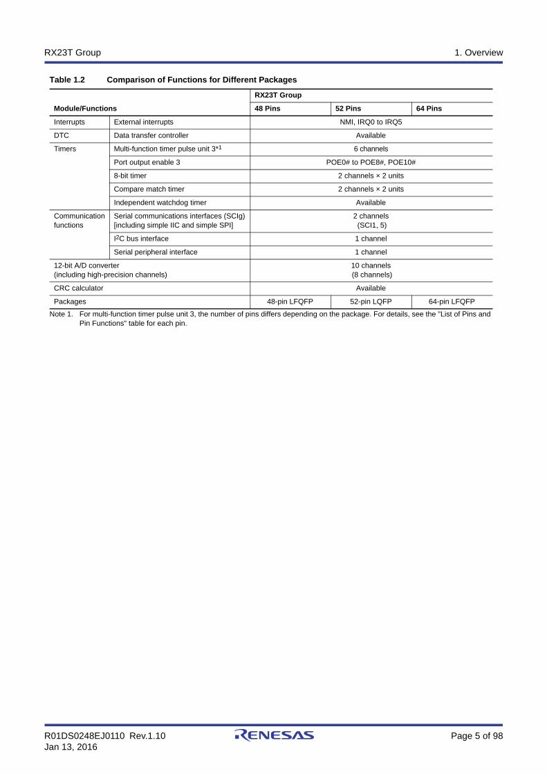
Note 1. For multi-function timer pulse unit 3, the number of pins differs depending on the package. For details, see the "List of Pins and Pin Functions" table for each pin.
Table 1.2 Comparison of Functions for Different Packages
Module/Functions
RX23T Group
48 Pins 52 Pins 64 Pins
Interrupts External interrupts NMI, IRQ0 to IRQ5
DTC Data transfer controller Available
Timers Multi-function timer pulse unit 3*1 6 channels
Port output enable 3 POE0# to POE8#, POE10#
8-bit timer 2 channels × 2 units
Compare match timer 2 channels × 2 units
Independent watchdog timer Available
Communicationfunctions
Serial communications interfaces (SCIg)[including simple IIC and simple SPI]
2 channels (SCI1, 5)
I2C bus interface 1 channel
Serial peripheral interface 1 channel
12-bit A/D converter(including high-precision channels)
10 channels (8 channels)
CRC calculator Available
Packages 48-pin LFQFP 52-pin LQFP 64-pin LFQFP

R01DS0248EJ0110 Rev.1.10 Page 6 of 98Jan 13, 2016
RX23T Group 1. Overview
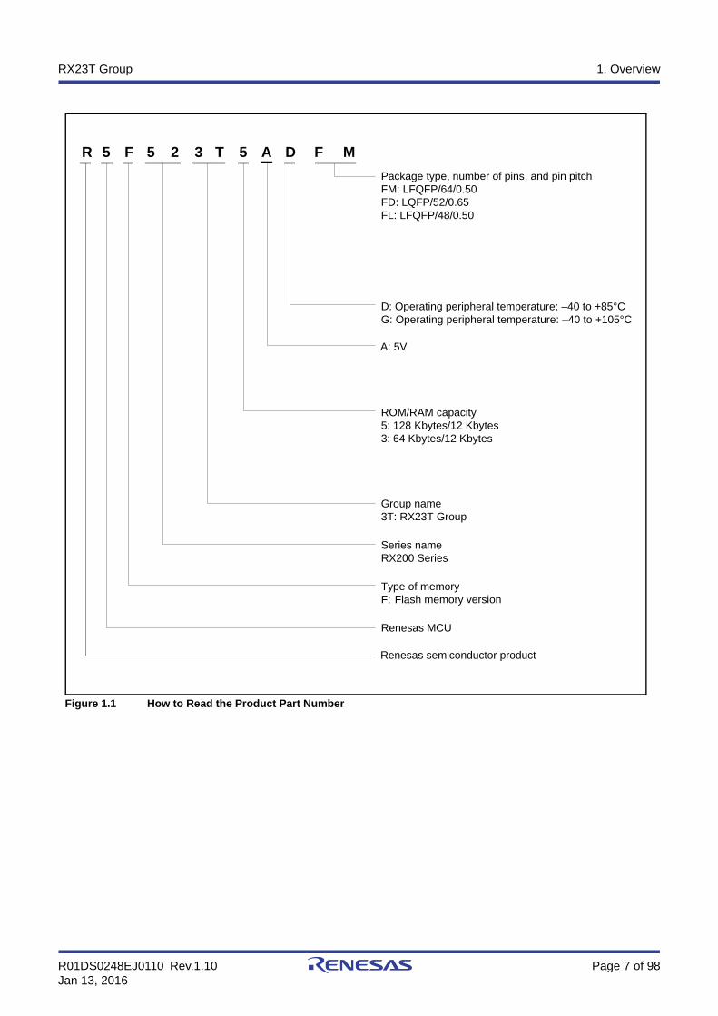
1.2 List of Products
Table 1.3 and Table 1.4 are a list of products, and Figure 1.1 shows how to read the product part no., memory capacity,
and package type.
Table 1.3 List of Products: D Version (Ta = –40 to +85°C)
Group Part No. Package ROM Capacity RAM CapacityOperatingFrequency
OperatingTemperature
RX23T R5F523T5ADFL PLQP0048KB-B 128 Kbytes 12 Kbytes 40MHz -40 to + 85°C
R5F523T5ADFD PLQP0052JA-B
R5F523T5ADFM PLQP0064KB-C
R5F523T3ADFL PLQP0048KB-B 64 Kbytes
R5F523T3ADFD PLQP0052JA-B
R5F523T3ADFM PLQP0064KB-C
Table 1.4 List of Products: G Version (Ta = –40 to +105°C)
Group Part No. Package ROM Capacity RAM CapacityOperatingFrequency
OperatingTemperature
RX23T R5F523T5AGFL PLQP0048KB-B 128 Kbytes 12 Kbytes 40MHz -40 to +105°C
R5F523T5AGFD PLQP0052JA-B
R5F523T5AGFM PLQP0064KB-C
R5F523T3AGFL PLQP0048KB-B 64 Kbytes
R5F523T3AGFD PLQP0052JA-B
R5F523T3AGFM PLQP0064KB-C
R01DS0248EJ0110 Rev.1.10 Page 7 of 98Jan 13, 2016
RX23T Group 1. Overview
Figure 1.1 How to Read the Product Part Number
Type of memory F: Flash memory version
Package type, number of pins, and pin pitchFM: LFQFP/64/0.50FD: LQFP/52/0.65FL: LFQFP/48/0.50
ROM/RAM capacity5: 128 Kbytes/12 Kbytes3: 64 Kbytes/12 Kbytes
Group name3T: RX23T Group
Renesas MCU
Renesas semiconductor product
Series nameRX200 Series
R 5 F 5 2 D F MA5T3
D: Operating peripheral temperature: –40 to +85°CG: Operating peripheral temperature: –40 to +105°C
A: 5V

R01DS0248EJ0110 Rev.1.10 Page 8 of 98Jan 13, 2016
RX23T Group 1. Overview
1.3 Block Diagram
Figure 1.2 shows a block diagram.
Figure 1.2 Block Diagram
12-bit A/D converter × 10 channels
MTU3c × 6ch
CMT × 2 channels (unit 0)
POE3b
TMR × 2 channels (unit 0)
TMR × 2 channels (unit 1)
CMT × 2 channels (unit 1)
RIICa × 1ch
RSPIa × 1ch
SCIg × 2ch
CRC
IWDTa
Clockgeneration
circuit
RX CPU
RAM
ROM
DOC
DTCa
ICUb
CAC
Comparator C × 3 channels
MPU
Op
eran
d b
us
Inst
ruct
ion
bus
Inte
rnal
mai
n bu
s 1 Inte
rna
l ma
in b
us 2
Inte
rnal
per
iph
eral
bus
es
1 to
6
Port D
Port E
Port A
Port B
Port 9
Port 7
Port 0
Port 1
Port 3
Port 4
Port 2
ICUb: Interrupt controllerDTCa: Data transfer controllerIWDTa: Independent watchdog timerCRC: CRC (cyclic redundancy check) calculatorSCIg: Serial communications interfaceRSPIa: Serial peripheral interfaceRIICa I2C bus interface
MTU3c Multi-function timer pulse unit 3POE3b Port output enable 3CMT Compare match timerDOC Data operation circuitCAC Clock frequency accuracy measurement circuitMPU Memory protection unitTMR 8-bit timer

R01DS0248EJ0110 Rev.1.10 Page 9 of 98Jan 13, 2016
RX23T Group 1. Overview
1.4 Pin Functions
Table 1.5 lists the pin functions.
Table 1.5 Pin Functions (1/2)
Classifications Pin Name I/O Description
Power supply VCC Input Power supply pin. Connect it to the system power supply.
VCL — Connect this pin to the VSS pin via the 4.7 μF smoothing capacitor used to stabilize the internal power supply. Place the capacitor close to the pin.
VSS Input Ground pin. Connect it to the system power supply (0 V).
Clock XTAL Output Pins for connecting a crystal. An external clock can be input through the EXTAL pin.
EXTAL Input
Operating mode control
MD Input Pin for setting the operating mode. The signal levels on this pin must not be changed during operation.
System control RES# Input Reset pin. This MCU enters the reset state when this signal goes low.
CAC CACREF Input Input pin for the clock frequency accuracy measurement circuit.
On-chip emulator
FINED I/O FINE interface pin.
Interrupts NMI Input Non-maskable interrupt request pin.
IRQ0 to IRQ5 Input Interrupt request pins.
Multi-function timer pulse unit 3
MTIOC0A, MTIOC0BMTIOC0C, MTIOC0D
I/O The TGRA0 to TGRD0 input capture input/output compare output/PWM output pins.
MTIOC1A, MTIOC1B I/O The TGRA1 and TGRB1 input capture input/output compare output/PWM output pins.
MTIOC2A, MTIOC2B I/O The TGRA2 and TGRB2 input capture input/output compare output/PWM output pins.
MTIOC3A, MTIOC3BMTIOC3C, MTIOC3D
I/O The TGRA3 to TGRD3 input capture input/output compare output/PWM output pins.
MTIOC4A, MTIOC4BMTIOC4C, MTIOC4D
I/O The TGRA4 to TGRD4 input capture input/output compare output/PWM output pins.
MTIC5U, MTIC5V, MTIC5W Input The TGRU5, TGRV5, and TGRW5 input capture input/external pulse input pins.
MTCLKA, MTCLKB, MTCLKC, MTCLKD
Input Input pins for the external clock.
ADSM0 Output A/D trigger output pin.
Port output enable 3
POE0#, POE8#, POE10# Input Input pins for request signals to place the MTU pins in the high impedance state.
8-bit timer TMO0 to TMO3 Output Compare match output pins.
TMCI0 to TMCI3 Input Input pins for the external clock to be input to the counter.
TMRI0 to TMRI3 Input Counter reset input pins.
Serial communications interface (SCIg)
Asynchronous mode/clock synchronous mode
SCK1, SCK5 I/O Input/output pins for the clock.
RXD1, RXD5 Input Input pins for received data.
TXD1, TXD5 Output Output pins for transmitted data.
CTS1#, CTS5# Input Input pins for controlling the start of transmission and reception.
RTS1#, RTS5# Output Output pins for controlling the start of transmission and reception.
Simple I2C mode
SSCL1, SSCL5 I/O Input/output pins for the I2C clock.
SSDA1, SSDA5 I/O Input/output pins for the I2C data.

R01DS0248EJ0110 Rev.1.10 Page 10 of 98Jan 13, 2016
RX23T Group 1. Overview
Serial communications interface (SCIg)
Simple SPI mode
SCK1, SCK5 I/O Input/output pins for the clock.
SMISO1, SMISO5 I/O Input/output pins for slave transmit data.
SMOSI1, SMOSI5 I/O Input/output pins for master transmit data.
SS1#, SS5# Input Chip-select input pins.
I2C bus interface SCL0 I/O Input/output pin for I2C bus interface clocks. Bus can be directly driven by the N-channel open drain output.
SDA0 I/O Input/output pin for I2C bus interface data. Bus can be directly driven by the N-channel open drain output.
Serial peripheral interface
RSPCKA I/O Input/output pin for the RSPI clock.
MOSIA I/O Input/output pin for transmitting data from the RSPI master.
MISOA I/O Input/output pin for transmitting data from the RSPI slave.
SSLA0 I/O Input/output pin to select the slave for the RSPI.
SSLA1 to SSLA3 Output Output pins to select the slave for the RSPI.
12-bit A/D converter
AN000 to AN007, AN016, AN017
Input Input pins for the analog signals to be processed by the A/D converter.
ADTRG0# Input Input pin for the external trigger signals that start the A/D conversion.
ADST0 Output Output pin for A/D conversion status.
Comparator C CMPC00, CMPC01, CMPC02
Input Analog input pin for CMPC0
CMPC10, CMPC11, CMPC12
Input Analog input pin for CMPC1
CMPC20, CMPC21, CMPC22
Input Analog input pin for CMPC2
COMP0 to COMP2 Output Comparator detection result output pins.
CVREFC0, CVREFC1 Input Analog reference voltage supply pins for comparator C.
Analog power supply
AVCC0 Input Analog voltage supply pin for the 12-bit A/D converter, comparator C, and the 8-bit D/A converter for generating comparator C reference voltage. Connect this pin to VCC when these modules are not used.
AVSS0 Input Analog ground pin for the 12-bit A/D converter, comparator C, and the 8-bit D/A converter for generating comparator C reference voltage. Connect this pin to VSS when these modules are not used.
VREFH0 Input Analog reference voltage supply pin for the 12-bit A/D converter.
VREFL0 Input Analog reference ground pin for the 12-bit A/D converter.
I/O ports P00 to P02 I/O 3-bit input/output pins.
P10, P11 I/O 2-bit input/output pins.
P22 to P24 I/O 3-bit input/output pins.
P30 to P33, P36, P37 I/O 6-bit input/output pins.
P40 to P47 I/O 8-bit input/output pins.
P70 to P76 I/O 7-bit input/output pins.
P91 to P94 I/O 4-bit input/output pins.
PA2 to PA5 I/O 4-bit input/output pins.
PB0 to PB7 I/O 8-bit input/output pins.
PD3 to PD7 I/O 5-bit input/output pins.
PE2 Input 1-bit input pin.
Table 1.5 Pin Functions (2/2)
Classifications Pin Name I/O Description

R01DS0248EJ0110 Rev.1.10 Page 11 of 98Jan 13, 2016
RX23T Group 1. Overview
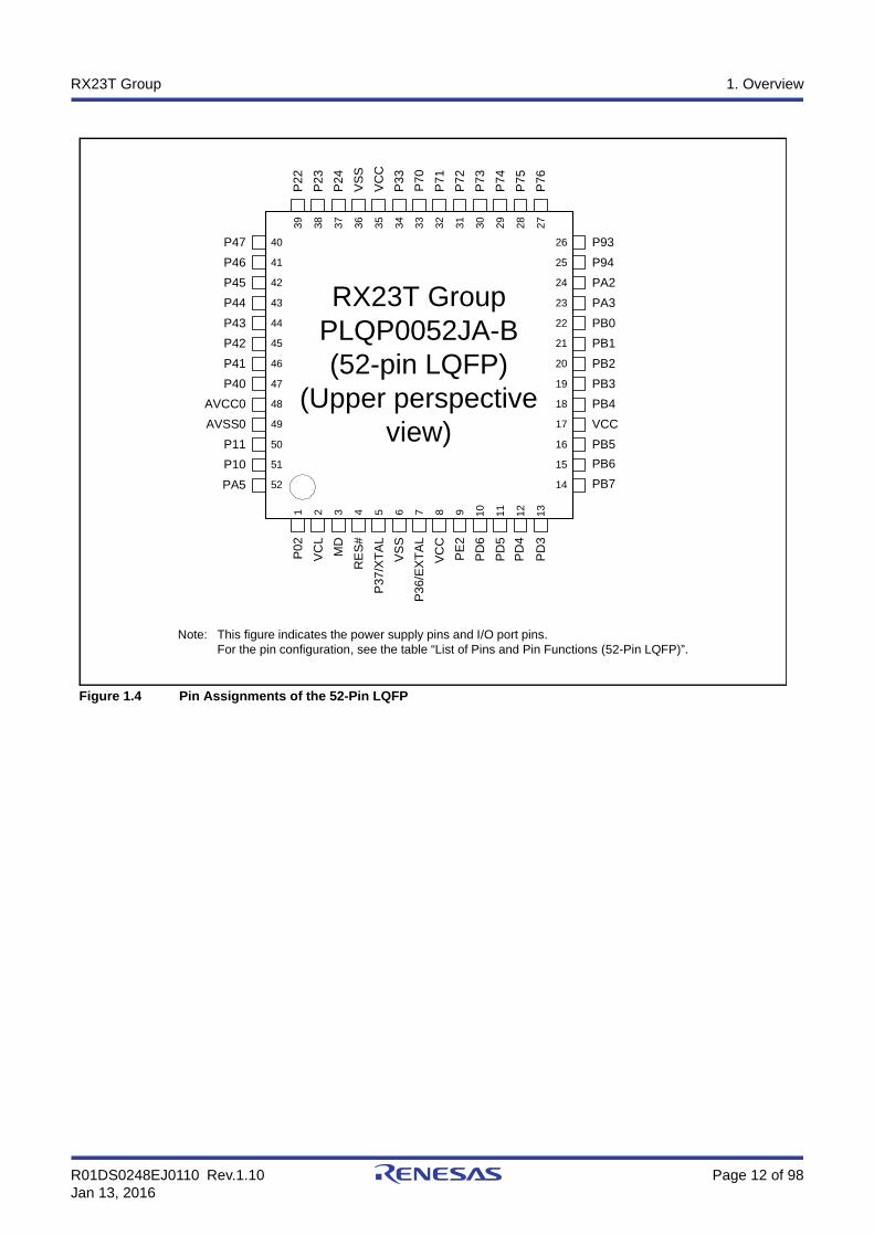
1.5 Pin Assignments
Figure 1.3 to Figure 1.5 show the pin assignments. Table 1.6 to Table 1.8 show the lists of pins and pin functions.
Figure 1.3 Pin Assignments of the 64-Pin LFQFP
48
47
46
45
44
43
42
41
40
39
38
37
36
35
34
33
32
31
30
29
28
27
26
25
24
23
22
21
20
19
18
17
1 2 3 4 5 6 7 8 9 10
11
12
13
14
15 16
54
55
51
49
50
52
53
56
57
58
59
60
61
63
64
62
RX23T GroupPLQP0064KB-C(64-pin LFQFP)
(Upper perspective view)
P47
P46
P45
P44
P43
P42
P41
P40
AVCC0
VREFH0
VREFL0
AVSS0
P11
P10
PA5
PA4
P22
P23
P24
P30
VS
S
P31
VC
C
P32
P33
P70
P71
P72
P73
P74
P75
P76
P91
P92
P93
P94
PA2
PA3
PB0
PB1
PB2
PB3
VSS
PB4
VCC
PB5
PB6
PB7
P0
2
P0
0
VC
L
P0
1
MD
RE
S#
P3
7/X
TA
L
VS
S
P3
6/E
XT
AL
VC
C
PE
2
PD
7
PD
6
PD
5
PD
4
PD
3
This figure indicates the power supply pins and I/O port pins. For the pin configuration, see the table “List of Pins and Pin Functions (64-Pin LFQFP)”.
Note:
R01DS0248EJ0110 Rev.1.10 Page 12 of 98Jan 13, 2016
RX23T Group 1. Overview
Figure 1.4 Pin Assignments of the 52-Pin LQFP
This figure indicates the power supply pins and I/O port pins. For the pin configuration, see the table “List of Pins and Pin Functions (52-Pin LQFP)”.
39 38 37 36 35 34 33 32 31 30 29 28 27
26
25
24
23
22
21
20
19
18
17
16
15
14
1 2 3 4 5 6 7 8 9 10 11 12 13
42
43
40
41
44
45
46
47
48
49
51
52
50
RX23T GroupPLQP0052JA-B(52-pin LQFP)
(Upper perspective view)
P47
P46
P45
P44
P43
P42
P41
P40
AVCC0
AVSS0
P11
P10
PA5
P2
2
P2
3
P2
4
VS
S
VC
C
P3
3
P7
0
P7
1
P7
2
P7
3
P7
4
P7
5
P7
6
P93
P94
PA2
PA3
PB0
PB1
PB2
PB3
PB4
VCC
PB5
PB6
PB7
P0
2
VC
L
MD
RE
S#
P3
7/X
TA
L
VS
S
P3
6/E
XT
AL
VC
C
PE
2
PD
6
PD
5
PD
4
PD
3
Note:

R01DS0248EJ0110 Rev.1.10 Page 13 of 98Jan 13, 2016
RX23T Group 1. Overview
Figure 1.5 Pin Assignments of the 48-Pin LFQFP
This figure indicates the power supply pins and I/O port pins. For the pin configuration, see the table “List of Pins and Pin Functions (48-Pin LFQFP)”.
36
35
34
33
32
31
30
29
28
27
26
25
24
23
22
21
20
19
1 2 3 4 5 6 7 8 9 10 11 12
38
39
37
40
41
42
43
44
45
47
48
46
RX23T GroupPLQP0048KB-B(48-pin LFQFP)
(Upper perspective view)
P47
P46
P45
P44
P43
P42
P41
P40
AVCC0
AVSS0
P11
P10
P2
2
P2
3
P2
4
VS
S
VC
C
P7
0
P7
1
P7
2
P7
3
P7
4
P7
5
P7
6
P93
P94
PA2
PA3
PB0
PB1
PB2
PB3
PB4
VCC
PB5
PB6
VC
L
MD
RE
S#
P3
7/X
TA
L
VS
S
P36
/EX
TA
L
VC
C
PE
2
PD
6
PD
5
PD
4
PD
3
18
17
16
15
14
13
Note:
R01DS0248EJ0110 Rev.1.10 Page 14 of 98Jan 13, 2016
RX23T Group 1. Overview
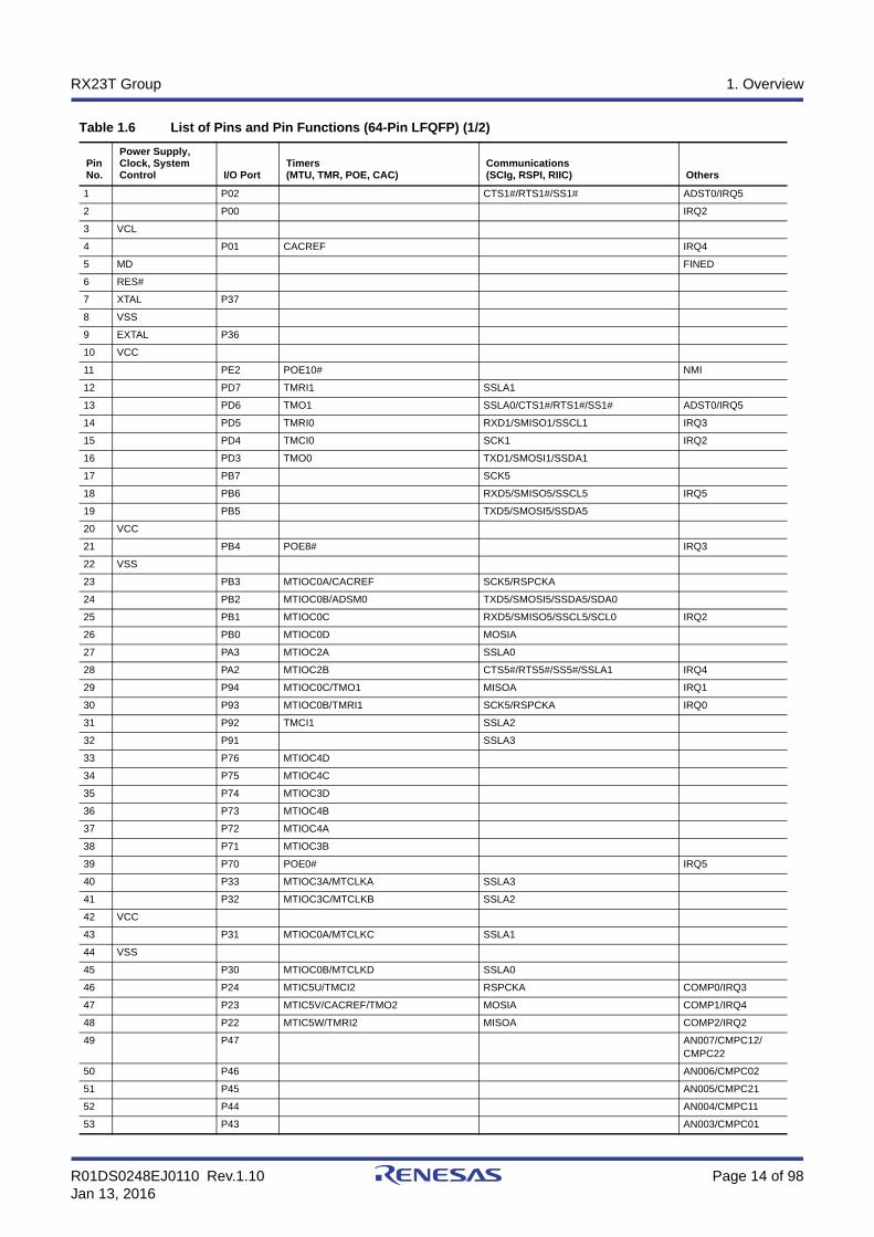
Table 1.6 List of Pins and Pin Functions (64-Pin LFQFP) (1/2)
Pin No.
Power Supply, Clock, System Control I/O Port
Timers(MTU, TMR, POE, CAC)
Communications(SCIg, RSPI, RIIC) Others
1 P02 CTS1#/RTS1#/SS1# ADST0/IRQ5
2 P00 IRQ2
3 VCL
4 P01 CACREF IRQ4
5 MD FINED
6 RES#
7 XTAL P37
8 VSS
9 EXTAL P36
10 VCC
11 PE2 POE10# NMI
12 PD7 TMRI1 SSLA1
13 PD6 TMO1 SSLA0/CTS1#/RTS1#/SS1# ADST0/IRQ5
14 PD5 TMRI0 RXD1/SMISO1/SSCL1 IRQ3
15 PD4 TMCI0 SCK1 IRQ2
16 PD3 TMO0 TXD1/SMOSI1/SSDA1
17 PB7 SCK5
18 PB6 RXD5/SMISO5/SSCL5 IRQ5
19 PB5 TXD5/SMOSI5/SSDA5
20 VCC
21 PB4 POE8# IRQ3
22 VSS
23 PB3 MTIOC0A/CACREF SCK5/RSPCKA
24 PB2 MTIOC0B/ADSM0 TXD5/SMOSI5/SSDA5/SDA0
25 PB1 MTIOC0C RXD5/SMISO5/SSCL5/SCL0 IRQ2
26 PB0 MTIOC0D MOSIA
27 PA3 MTIOC2A SSLA0
28 PA2 MTIOC2B CTS5#/RTS5#/SS5#/SSLA1 IRQ4
29 P94 MTIOC0C/TMO1 MISOA IRQ1
30 P93 MTIOC0B/TMRI1 SCK5/RSPCKA IRQ0
31 P92 TMCI1 SSLA2
32 P91 SSLA3
33 P76 MTIOC4D
34 P75 MTIOC4C
35 P74 MTIOC3D
36 P73 MTIOC4B
37 P72 MTIOC4A
38 P71 MTIOC3B
39 P70 POE0# IRQ5
40 P33 MTIOC3A/MTCLKA SSLA3
41 P32 MTIOC3C/MTCLKB SSLA2
42 VCC
43 P31 MTIOC0A/MTCLKC SSLA1
44 VSS
45 P30 MTIOC0B/MTCLKD SSLA0
46 P24 MTIC5U/TMCI2 RSPCKA COMP0/IRQ3
47 P23 MTIC5V/CACREF/TMO2 MOSIA COMP1/IRQ4
48 P22 MTIC5W/TMRI2 MISOA COMP2/IRQ2
49 P47 AN007/CMPC12/CMPC22
50 P46 AN006/CMPC02
51 P45 AN005/CMPC21
52 P44 AN004/CMPC11
53 P43 AN003/CMPC01

R01DS0248EJ0110 Rev.1.10 Page 15 of 98Jan 13, 2016
RX23T Group 1. Overview
54 P42 AN002/CMPC20
55 P41 AN001/CMPC10
56 P40 AN000/CMPC00
57 AVCC0
58 VREFH0
59 VREFL0
60 AVSS0
61 P11 MTIOC3A/MTCLKC/TMO3 IRQ1/AN016/CVREFC0
62 P10 MTCLKD/TMRI3 IRQ0/AN017/CVREFC1
63 PA5 MTIOC1A/TMCI3 MISOA
64 PA4 MTIOC1B RSPCKA ADTRG0#
Table 1.6 List of Pins and Pin Functions (64-Pin LFQFP) (2/2)
Pin No.
Power Supply, Clock, System Control I/O Port
Timers(MTU, TMR, POE, CAC)
Communications(SCIg, RSPI, RIIC) Others
R01DS0248EJ0110 Rev.1.10 Page 16 of 98Jan 13, 2016
RX23T Group 1. Overview
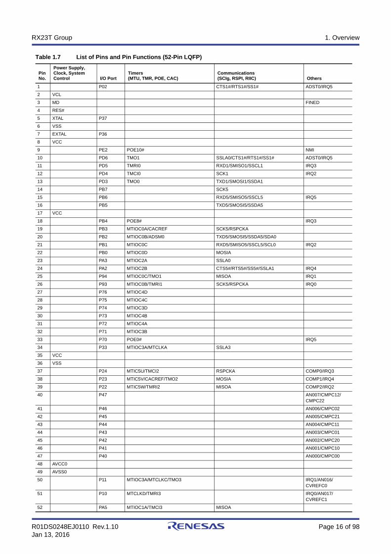
Table 1.7 List of Pins and Pin Functions (52-Pin LQFP)
Pin No.
Power Supply, Clock, System Control I/O Port
Timers(MTU, TMR, POE, CAC)
Communications(SCIg, RSPI, RIIC) Others
1 P02 CTS1#/RTS1#/SS1# ADST0/IRQ5
2 VCL
3 MD FINED
4 RES#
5 XTAL P37
6 VSS
7 EXTAL P36
8 VCC
9 PE2 POE10# NMI
10 PD6 TMO1 SSLA0/CTS1#/RTS1#/SS1# ADST0/IRQ5
11 PD5 TMRI0 RXD1/SMISO1/SSCL1 IRQ3
12 PD4 TMCI0 SCK1 IRQ2
13 PD3 TMO0 TXD1/SMOSI1/SSDA1
14 PB7 SCK5
15 PB6 RXD5/SMISO5/SSCL5 IRQ5
16 PB5 TXD5/SMOSI5/SSDA5
17 VCC
18 PB4 POE8# IRQ3
19 PB3 MTIOC0A/CACREF SCK5/RSPCKA
20 PB2 MTIOC0B/ADSM0 TXD5/SMOSI5/SSDA5/SDA0
21 PB1 MTIOC0C RXD5/SMISO5/SSCL5/SCL0 IRQ2
22 PB0 MTIOC0D MOSIA
23 PA3 MTIOC2A SSLA0
24 PA2 MTIOC2B CTS5#/RTS5#/SS5#/SSLA1 IRQ4
25 P94 MTIOC0C/TMO1 MISOA IRQ1
26 P93 MTIOC0B/TMRI1 SCK5/RSPCKA IRQ0
27 P76 MTIOC4D
28 P75 MTIOC4C
29 P74 MTIOC3D
30 P73 MTIOC4B
31 P72 MTIOC4A
32 P71 MTIOC3B
33 P70 POE0# IRQ5
34 P33 MTIOC3A/MTCLKA SSLA3
35 VCC
36 VSS
37 P24 MTIC5U/TMCI2 RSPCKA COMP0/IRQ3
38 P23 MTIC5V/CACREF/TMO2 MOSIA COMP1/IRQ4
39 P22 MTIC5W/TMRI2 MISOA COMP2/IRQ2
40 P47 AN007/CMPC12/CMPC22
41 P46 AN006/CMPC02
42 P45 AN005/CMPC21
43 P44 AN004/CMPC11
44 P43 AN003/CMPC01
45 P42 AN002/CMPC20
46 P41 AN001/CMPC10
47 P40 AN000/CMPC00
48 AVCC0
49 AVSS0
50 P11 MTIOC3A/MTCLKC/TMO3 IRQ1/AN016/CVREFC0
51 P10 MTCLKD/TMRI3 IRQ0/AN017/CVREFC1
52 PA5 MTIOC1A/TMCI3 MISOA
R01DS0248EJ0110 Rev.1.10 Page 17 of 98Jan 13, 2016
RX23T Group 1. Overview
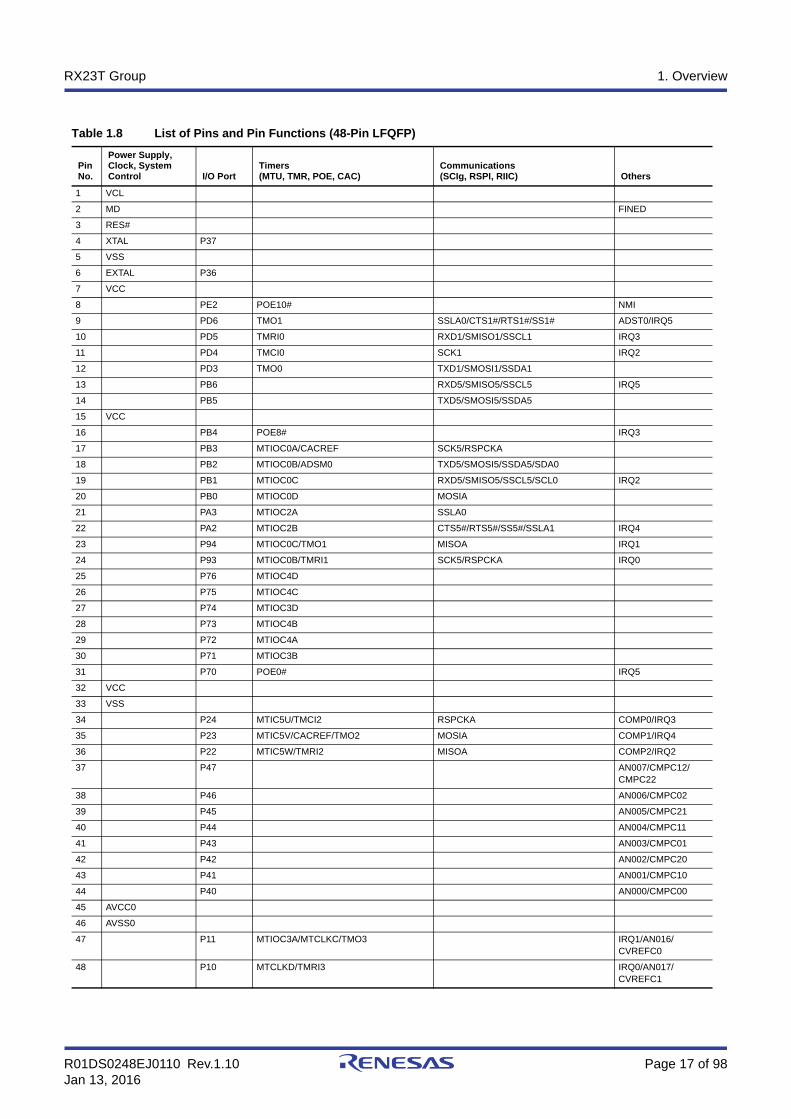
Table 1.8 List of Pins and Pin Functions (48-Pin LFQFP)
Pin No.
Power Supply, Clock, System Control I/O Port
Timers(MTU, TMR, POE, CAC)
Communications(SCIg, RSPI, RIIC) Others
1 VCL
2 MD FINED
3 RES#
4 XTAL P37
5 VSS
6 EXTAL P36
7 VCC
8 PE2 POE10# NMI
9 PD6 TMO1 SSLA0/CTS1#/RTS1#/SS1# ADST0/IRQ5
10 PD5 TMRI0 RXD1/SMISO1/SSCL1 IRQ3
11 PD4 TMCI0 SCK1 IRQ2
12 PD3 TMO0 TXD1/SMOSI1/SSDA1
13 PB6 RXD5/SMISO5/SSCL5 IRQ5
14 PB5 TXD5/SMOSI5/SSDA5
15 VCC
16 PB4 POE8# IRQ3
17 PB3 MTIOC0A/CACREF SCK5/RSPCKA
18 PB2 MTIOC0B/ADSM0 TXD5/SMOSI5/SSDA5/SDA0
19 PB1 MTIOC0C RXD5/SMISO5/SSCL5/SCL0 IRQ2
20 PB0 MTIOC0D MOSIA
21 PA3 MTIOC2A SSLA0
22 PA2 MTIOC2B CTS5#/RTS5#/SS5#/SSLA1 IRQ4
23 P94 MTIOC0C/TMO1 MISOA IRQ1
24 P93 MTIOC0B/TMRI1 SCK5/RSPCKA IRQ0
25 P76 MTIOC4D
26 P75 MTIOC4C
27 P74 MTIOC3D
28 P73 MTIOC4B
29 P72 MTIOC4A
30 P71 MTIOC3B
31 P70 POE0# IRQ5
32 VCC
33 VSS
34 P24 MTIC5U/TMCI2 RSPCKA COMP0/IRQ3
35 P23 MTIC5V/CACREF/TMO2 MOSIA COMP1/IRQ4
36 P22 MTIC5W/TMRI2 MISOA COMP2/IRQ2
37 P47 AN007/CMPC12/CMPC22
38 P46 AN006/CMPC02
39 P45 AN005/CMPC21
40 P44 AN004/CMPC11
41 P43 AN003/CMPC01
42 P42 AN002/CMPC20
43 P41 AN001/CMPC10
44 P40 AN000/CMPC00
45 AVCC0
46 AVSS0
47 P11 MTIOC3A/MTCLKC/TMO3 IRQ1/AN016/CVREFC0
48 P10 MTCLKD/TMRI3 IRQ0/AN017/CVREFC1

R01DS0248EJ0110 Rev.1.10 Page 18 of 98Jan 13, 2016
RX23T Group 2. CPU
2. CPUFigure 2.1 shows register set of the CPU.
Figure 2.1 Register Set of the CPU
Note 1. The stack pointer (SP) can be the interrupt stack pointer (ISP) or user stack pointer (USP), according to the value of the U bit in the PSW.
R15
R14
R13
R12
R11
R10
R9
R8
R7
R6
R5
R4
R3
R2
R1
R0 (SP)*1
General-purpose register
b31 b0
DSP instruction register
b71 b0
ACC0 (Accumulator 0)
ACC1 (Accumulator 1)
USP (User stack pointer)
ISP (Interrupt stack pointer)
INTB (Interrupt table register)
PC (Program counter)
PSW (Processor status word)
BPC (Backup PC)
BPSW (Backup PSW)
FINTV (Fast interrupt vector register)
FPSW (Floating-point status word)
Control registerb31 b0
EXTB (Exception table register)

R01DS0248EJ0110 Rev.1.10 Page 19 of 98Jan 13, 2016
RX23T Group 2. CPU
2.1 General-Purpose Registers (R0 to R15)
This CPU has sixteen 32-bit general-purpose registers (R0 to R15). R0 to R15 can be used as data registers or address
registers.
R0, a general-purpose register, also functions as the stack pointer (SP).
The stack pointer is switched to operate as the interrupt stack pointer (ISP) or user stack pointer (USP) by the value of the
stack pointer select bit (U) in the processor status word (PSW).
2.2 Control Registers
(1) Interrupt stack pointer (ISP) and user stack pointer (USP)
The stack pointer (SP) can be either of two types, the interrupt stack pointer (ISP) or the user stack pointer (USP).
Whether the stack pointer operates as the ISP or USP depends on the value of the stack pointer select bit (U) in the
processor status word (PSW).
Set the ISP or USP to a multiple of 4 to reduce the number of cycles required to execute interrupt sequences and
instructions entailing stack manipulation.
(2) Exception table register (EXTB)
The exception table register (EXTB) specifies the address where the exception vector table starts.
Set the EXTB to a multiple of 4 to reduce the number of cycles required to execute interrupt sequences and instructions
entailing stack manipulation.
(3) Interrupt table register (INTB)
The interrupt table register (INTB) specifies the address where the interrupt vector table starts.
Set the INTB to a multiple of 4 to reduce the number of cycles required to execute interrupt sequences and instructions
entailing stack manipulation.
(4) Program counter (PC)
The program counter (PC) indicates the address of the instruction being executed.
(5) Processor status word (PSW)
The processor status word (PSW) indicates the results of instruction execution or the state of the CPU.
(6) Backup PC (BPC)
The backup PC (BPC) is provided to speed up response to interrupts.
After a fast interrupt has been generated, the contents of the program counter (PC) are saved in the BPC register.
(7) Backup PSW (BPSW)
The backup PSW (BPSW) is provided to speed up response to interrupts.
After a fast interrupt has been generated, the contents of the processor status word (PSW) are saved in the BPSW. The
allocation of bits in the BPSW corresponds to that in the PSW.
(8) Fast interrupt vector register (FINTV)
The fast interrupt vector register (FINTV) is provided to speed up response to interrupts.
The FINTV register specifies a branch destination address when a fast interrupt has been generated.

R01DS0248EJ0110 Rev.1.10 Page 20 of 98Jan 13, 2016
RX23T Group 2. CPU
(9) Floating-point status word (FPSW)
The floating-point status word (FPSW) indicates the results of floating-point operations.
When an exception handling enable bit (Ej) enables the exception handling (Ej = 1), the exception cause can be identified
by checking the corresponding Cj flag in the exception handling routine. If the exception handling is masked (Ej = 0), the
occurrence of exception can be checked by reading the Fj flag at the end of a series of processing. Once the Fj flag has
been set to 1, this value is retained until it is cleared to 0 by software (j = X, U, Z, O, or V).
2.3 Accumulator
The accumulator (ACC0 or ACC1) is a 72-bit register used for DSP instructions. The accumulator is handled as a 96-bit
register for reading and writing. At this time, when bits 95 to 72 of the accumulator are read, the value where the value of
bit 71 is sign extended is read. Writing to bits 95 to 72 of the accumulator is ignored. ACC0 is also used for the multiply
and multiply-and-accumulate instructions; EMUL, EMULU, FMUL, MUL, and RMPA, in which case the prior value in
ACC0 is modified by execution of the instruction.
Use the MVTACGU, MVTACHI, and MVTACLO instructions for writing to the accumulator. The MVTACGU,
MVTACHI, and MVTACLO instructions write data to bits 95 to 64, the higher-order 32 bits (bits 63 to 32), and the
lower-order 32 bits (bits 31 to 0), respectively.
Use the MVFACGU, MVFACHI, MVFACMI, and MVFACLO instructions for reading data from the accumulator. The
MVFACGU, MVFACHI, MVFACMI, and MVFACLO instructions read data from the guard bits (bits 95 to 64), higher-
order 32 bits (bits 63 to 32), the middle 32 bits (bits 47 to 16), and the lower-order 32 bits (bits 31 to 0), respectively.
R01DS0248EJ0110 Rev.1.10 Page 21 of 98Jan 13, 2016
RX23T Group 3. Address Space
3. Address Space
3.1 Address Space
This LSI has a 4-Gbyte address space, consisting of the range of addresses from 0000 0000h to FFFF FFFFh. That is,
linear access to an address space of up to 4 Gbytes is possible, and this contains both program and data areas.
Figure 3.1 shows the memory maps in the respective operating modes. Accessible areas will differ according to the
operating mode and states of control bits.

R01DS0248EJ0110 Rev.1.10 Page 22 of 98Jan 13, 2016
RX23T Group 3. Address Space
Figure 3.1 Memory Map in Each Operating Mode
Reserved area*3
Reserved area*3
Reserved area*3
Reserved area*3
0000 0000h
0008 0000h
FFFF FFFFh
Single-chip mode*1
RAM*2
On-chip ROM (program ROM)(read only)*2
0010 0000h
Peripheral I/O registers
0080 0000h
FFFE 0000h
Peripheral I/O registers
Peripheral I/O registers
007F C000h007F C500h
007F FC00h
0000 2800h
RAM*20000 4000h
0008 4A80hReserved area*3
Note 1. The address space in boot mode is the same as the address space in single-chip mode.Note 2. The capacity of ROM/RAM differs depending on the products.
Note: See Table 1.3 and Table 1.4 List of Products, for the product type name.
Note 3. Reserved areas should not be accessed.
ROM (bytes) RAM (bytes)
Capacity Address Capacity Address
128 Kbytes FFFE 0000h to FFFF FFFFh 12 Kbytes 0000 0000h to 0000 27FFh0000 4000h to 0000 4A7Fh
64 Kbytes FFFF 0000h to FFFF FFFFh
R01DS0248EJ0110 Rev.1.10 Page 23 of 98Jan 13, 2016
RX23T Group 4. I/O Registers
4. I/O RegistersThis section provides information on the on-chip I/O register addresses and bit configuration. The information is given as
shown below. Notes on writing to registers are also given below.
(1) I/O register addresses (address order)
Registers are listed from the lower allocation addresses.
Registers are classified according to module symbols.
Numbers of cycles for access indicate numbers of cycles of the given base clock.
Among the internal I/O register area, addresses not listed in the list of registers are reserved. Reserved addresses
must not be accessed. Do not access these addresses; otherwise, the operation when accessing these bits and
subsequent operations cannot be guaranteed.
(2) Notes on writing to I/O registers
When writing to an I/O register, the CPU starts executing the subsequent instruction before completing I/O register write.
This may cause the subsequent instruction to be executed before the post-update I/O register value is reflected on the
operation.
As described in the following examples, special care is required for the cases in which the subsequent instruction must be
executed after the post-update I/O register value is actually reflected.
[Examples of cases requiring special care]
The subsequent instruction must be executed while an interrupt request is disabled with the IENj bit in IERn of the
ICU (interrupt request enable bit) cleared to 0.
A WAIT instruction is executed immediately after the preprocessing for causing a transition to the low power
consumption state.
In the above cases, after writing to an I/O register, wait until the write operation is completed using the following
procedure and then execute the subsequent instruction.
(a) Write to an I/O register.
(b) Read the value from the I/O register to a general register.
(c) Execute the operation using the value read.
(d) Execute the subsequent instruction.
[Instruction examples]
Byte-size I/O registers
MOV.L #SFR_ADDR, R1
MOV.B #SFR_DATA, [R1]
CMP [R1].UB, R1
;; Next process
Word-size I/O registers
MOV.L #SFR_ADDR, R1
MOV.W #SFR_DATA, [R1]
CMP [R1].W, R1
;; Next process

R01DS0248EJ0110 Rev.1.10 Page 24 of 98Jan 13, 2016
RX23T Group 4. I/O Registers
Longword-size I/O registers
MOV.L #SFR_ADDR, R1
MOV.L #SFR_DATA, [R1]
CMP [R1].L, R1
;; Next process
If multiple registers are written to and a subsequent instruction should be executed after the write operations are entirely
completed, only read the I/O register that was last written to and execute the operation using the value; it is not necessary
to read or execute operation for all the registers that were written to.
(3) Number of Access Cycles to I/O Registers
For numbers of clock cycles for access to I/O registers, see Table 4.1, List of I/O Registers (Address Order).
The number of access cycles to I/O registers is obtained by following equation.*1
Number of access cycles to I/O registers = Number of bus cycles for internal main bus 1 +
Number of divided clock synchronization cycles +
Number of bus cycles for internal peripheral bus 1 to 6
The number of bus cycles of internal peripheral bus 1 to 6 differs according to the register to be accessed.
When peripheral functions connected to internal peripheral bus 2 to 6 are accessed, the number of divided clock
synchronization cycles is added.
In the peripheral function unit, when the frequency ratio of ICLK is equal to or greater than that of PCLK (or FCLK), the
sum of the number of bus cycles for internal main bus 1 and the number of the divided clock synchronization cycles will
be one cycle of PCLK (or FCLK) at a maximum. Therefore, one PCLK (or FCLK) has been added to the number of
access cycles shown in Table 4.1.
Note 1. This applies to the number of cycles when the access from the CPU does not conflict with the bus access from the different bus master (DTC).
(4) Restrictions in Relation to RMPA and String-Manipulation Instructions
The allocation of data to be handled by RMPA or string-manipulation instructions to I/O registers is prohibited, and
operation is not guaranteed if this restriction is not observed.
(5) Notes on Sleep Mode and Mode Transitions
During sleep mode or mode transitions, do not write to the system control related registers (indicated by 'SYSTEM' in the
Module Symbol column in Table 4.1, List of I/O Registers (Address Order)).
R01DS0248EJ0110 Rev.1.10 Page 25 of 98Jan 13, 2016
RX23T Group 4. I/O Registers
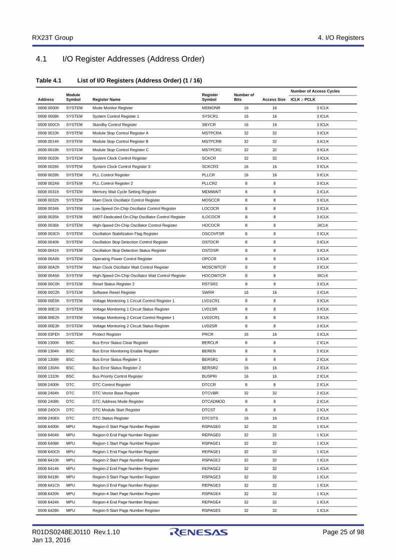
4.1 I/O Register Addresses (Address Order)
Table 4.1 List of I/O Registers (Address Order) (1 / 16)
AddressModule Symbol Register Name
Register Symbol
Number of Bits Access Size
Number of Access Cycles
ICLK PCLK
0008 0000h SYSTEM Mode Monitor Register MDMONR 16 16 3 ICLK
0008 0008h SYSTEM System Control Register 1 SYSCR1 16 16 3 ICLK
0008 000Ch SYSTEM Standby Control Register SBYCR 16 16 3 ICLK
0008 0010h SYSTEM Module Stop Control Register A MSTPCRA 32 32 3 ICLK
0008 0014h SYSTEM Module Stop Control Register B MSTPCRB 32 32 3 ICLK
0008 0018h SYSTEM Module Stop Control Register C MSTPCRC 32 32 3 ICLK
0008 0020h SYSTEM System Clock Control Register SCKCR 32 32 3 ICLK
0008 0026h SYSTEM System Clock Control Register 3 SCKCR3 16 16 3 ICLK
0008 0028h SYSTEM PLL Control Register PLLCR 16 16 3 ICLK
0008 002Ah SYSTEM PLL Control Register 2 PLLCR2 8 8 3 ICLK
0008 0031h SYSTEM Memory Wait Cycle Setting Register MEMWAIT 8 8 3 ICLK
0008 0032h SYSTEM Main Clock Oscillator Control Register MOSCCR 8 8 3 ICLK
0008 0034h SYSTEM Low-Speed On-Chip Oscillator Control Register LOCOCR 8 8 3 ICLK
0008 0035h SYSTEM IWDT-Dedicated On-Chip Oscillator Control Register ILOCOCR 8 8 3 ICLK
0008 0036h SYSTEM High-Speed On-Chip Oscillator Control Register HOCOCR 8 8 3ICLK
0008 003Ch SYSTEM Oscillation Stabilization Flag Register OSCOVFSR 8 8 3 ICLK
0008 0040h SYSTEM Oscillation Stop Detection Control Register OSTDCR 8 8 3 ICLK
0008 0041h SYSTEM Oscillation Stop Detection Status Register OSTDSR 8 8 3 ICLK
0008 00A0h SYSTEM Operating Power Control Register OPCCR 8 8 3 ICLK
0008 00A2h SYSTEM Main Clock Oscillator Wait Control Register MOSCWTCR 8 8 3 ICLK
0008 00A5h SYSTEM High-Speed On-Chip Oscillator Wait Control Register HOCOWTCR 8 8 3ICLK
0008 00C0h SYSTEM Reset Status Register 2 RSTSR2 8 8 3 ICLK
0008 00C2h SYSTEM Software Reset Register SWRR 16 16 3 ICLK
0008 00E0h SYSTEM Voltage Monitoring 1 Circuit Control Register 1 LVD1CR1 8 8 3 ICLK
0008 00E1h SYSTEM Voltage Monitoring 1 Circuit Status Register LVD1SR 8 8 3 ICLK
0008 00E2h SYSTEM Voltage Monitoring 2 Circuit Control Register 1 LVD2CR1 8 8 3 ICLK
0008 00E3h SYSTEM Voltage Monitoring 2 Circuit Status Register LVD2SR 8 8 3 ICLK
0008 03FEh SYSTEM Protect Register PRCR 16 16 3 ICLK
0008 1300h BSC Bus Error Status Clear Register BERCLR 8 8 2 ICLK
0008 1304h BSC Bus Error Monitoring Enable Register BEREN 8 8 2 ICLK
0008 1308h BSC Bus Error Status Register 1 BERSR1 8 8 2 ICLK
0008 130Ah BSC Bus Error Status Register 2 BERSR2 16 16 2 ICLK
0008 1310h BSC Bus Priority Control Register BUSPRI 16 16 2 ICLK
0008 2400h DTC DTC Control Register DTCCR 8 8 2 ICLK
0008 2404h DTC DTC Vector Base Register DTCVBR 32 32 2 ICLK
0008 2408h DTC DTC Address Mode Register DTCADMOD 8 8 2 ICLK
0008 240Ch DTC DTC Module Start Register DTCST 8 8 2 ICLK
0008 240Eh DTC DTC Status Register DTCSTS 16 16 2 ICLK
0008 6400h MPU Region-0 Start Page Number Register RSPAGE0 32 32 1 ICLK
0008 6404h MPU Region-0 End Page Number Register REPAGE0 32 32 1 ICLK
0008 6408h MPU Region-1 Start Page Number Register RSPAGE1 32 32 1 ICLK
0008 640Ch MPU Region-1 End Page Number Register REPAGE1 32 32 1 ICLK
0008 6410h MPU Region-2 Start Page Number Register RSPAGE2 32 32 1 ICLK
0008 6414h MPU Region-2 End Page Number Register REPAGE2 32 32 1 ICLK
0008 6418h MPU Region-3 Start Page Number Register RSPAGE3 32 32 1 ICLK
0008 641Ch MPU Region-3 End Page Number Register REPAGE3 32 32 1 ICLK
0008 6420h MPU Region-4 Start Page Number Register RSPAGE4 32 32 1 ICLK
0008 6424h MPU Region-4 End Page Number Register REPAGE4 32 32 1 ICLK
0008 6428h MPU Region-5 Start Page Number Register RSPAGE5 32 32 1 ICLK
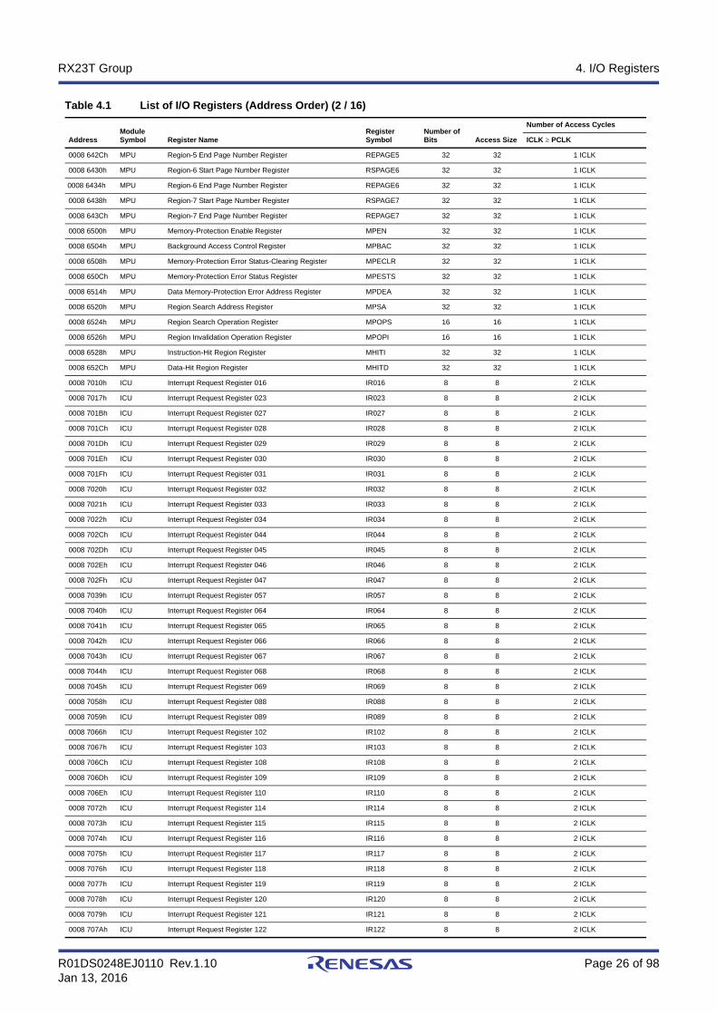
R01DS0248EJ0110 Rev.1.10 Page 26 of 98Jan 13, 2016
RX23T Group 4. I/O Registers
0008 642Ch MPU Region-5 End Page Number Register REPAGE5 32 32 1 ICLK
0008 6430h MPU Region-6 Start Page Number Register RSPAGE6 32 32 1 ICLK
0008 6434h MPU Region-6 End Page Number Register REPAGE6 32 32 1 ICLK
0008 6438h MPU Region-7 Start Page Number Register RSPAGE7 32 32 1 ICLK
0008 643Ch MPU Region-7 End Page Number Register REPAGE7 32 32 1 ICLK
0008 6500h MPU Memory-Protection Enable Register MPEN 32 32 1 ICLK
0008 6504h MPU Background Access Control Register MPBAC 32 32 1 ICLK
0008 6508h MPU Memory-Protection Error Status-Clearing Register MPECLR 32 32 1 ICLK
0008 650Ch MPU Memory-Protection Error Status Register MPESTS 32 32 1 ICLK
0008 6514h MPU Data Memory-Protection Error Address Register MPDEA 32 32 1 ICLK
0008 6520h MPU Region Search Address Register MPSA 32 32 1 ICLK
0008 6524h MPU Region Search Operation Register MPOPS 16 16 1 ICLK
0008 6526h MPU Region Invalidation Operation Register MPOPI 16 16 1 ICLK
0008 6528h MPU Instruction-Hit Region Register MHITI 32 32 1 ICLK
0008 652Ch MPU Data-Hit Region Register MHITD 32 32 1 ICLK
0008 7010h ICU Interrupt Request Register 016 IR016 8 8 2 ICLK
0008 7017h ICU Interrupt Request Register 023 IR023 8 8 2 ICLK
0008 701Bh ICU Interrupt Request Register 027 IR027 8 8 2 ICLK
0008 701Ch ICU Interrupt Request Register 028 IR028 8 8 2 ICLK
0008 701Dh ICU Interrupt Request Register 029 IR029 8 8 2 ICLK
0008 701Eh ICU Interrupt Request Register 030 IR030 8 8 2 ICLK
0008 701Fh ICU Interrupt Request Register 031 IR031 8 8 2 ICLK
0008 7020h ICU Interrupt Request Register 032 IR032 8 8 2 ICLK
0008 7021h ICU Interrupt Request Register 033 IR033 8 8 2 ICLK
0008 7022h ICU Interrupt Request Register 034 IR034 8 8 2 ICLK
0008 702Ch ICU Interrupt Request Register 044 IR044 8 8 2 ICLK
0008 702Dh ICU Interrupt Request Register 045 IR045 8 8 2 ICLK
0008 702Eh ICU Interrupt Request Register 046 IR046 8 8 2 ICLK
0008 702Fh ICU Interrupt Request Register 047 IR047 8 8 2 ICLK
0008 7039h ICU Interrupt Request Register 057 IR057 8 8 2 ICLK
0008 7040h ICU Interrupt Request Register 064 IR064 8 8 2 ICLK
0008 7041h ICU Interrupt Request Register 065 IR065 8 8 2 ICLK
0008 7042h ICU Interrupt Request Register 066 IR066 8 8 2 ICLK
0008 7043h ICU Interrupt Request Register 067 IR067 8 8 2 ICLK
0008 7044h ICU Interrupt Request Register 068 IR068 8 8 2 ICLK
0008 7045h ICU Interrupt Request Register 069 IR069 8 8 2 ICLK
0008 7058h ICU Interrupt Request Register 088 IR088 8 8 2 ICLK
0008 7059h ICU Interrupt Request Register 089 IR089 8 8 2 ICLK
0008 7066h ICU Interrupt Request Register 102 IR102 8 8 2 ICLK
0008 7067h ICU Interrupt Request Register 103 IR103 8 8 2 ICLK
0008 706Ch ICU Interrupt Request Register 108 IR108 8 8 2 ICLK
0008 706Dh ICU Interrupt Request Register 109 IR109 8 8 2 ICLK
0008 706Eh ICU Interrupt Request Register 110 IR110 8 8 2 ICLK
0008 7072h ICU Interrupt Request Register 114 IR114 8 8 2 ICLK
0008 7073h ICU Interrupt Request Register 115 IR115 8 8 2 ICLK
0008 7074h ICU Interrupt Request Register 116 IR116 8 8 2 ICLK
0008 7075h ICU Interrupt Request Register 117 IR117 8 8 2 ICLK
0008 7076h ICU Interrupt Request Register 118 IR118 8 8 2 ICLK
0008 7077h ICU Interrupt Request Register 119 IR119 8 8 2 ICLK
0008 7078h ICU Interrupt Request Register 120 IR120 8 8 2 ICLK
0008 7079h ICU Interrupt Request Register 121 IR121 8 8 2 ICLK
0008 707Ah ICU Interrupt Request Register 122 IR122 8 8 2 ICLK
Table 4.1 List of I/O Registers (Address Order) (2 / 16)
AddressModule Symbol Register Name
Register Symbol
Number of Bits Access Size
Number of Access Cycles
ICLK PCLK

R01DS0248EJ0110 Rev.1.10 Page 27 of 98Jan 13, 2016
RX23T Group 4. I/O Registers
0008 707Bh ICU Interrupt Request Register 123 IR123 8 8 2 ICLK
0008 707Ch ICU Interrupt Request Register 124 IR124 8 8 2 ICLK
0008 707Dh ICU Interrupt Request Register 125 IR125 8 8 2 ICLK
0008 707Eh ICU Interrupt Request Register 126 IR126 8 8 2 ICLK
0008 707Fh ICU Interrupt Request Register 127 IR127 8 8 2 ICLK
0008 7080h ICU Interrupt Request Register 128 IR128 8 8 2 ICLK
0008 7081h ICU Interrupt Request Register 129 IR129 8 8 2 ICLK
0008 7082h ICU Interrupt Request Register 130 IR130 8 8 2 ICLK
0008 7083h ICU Interrupt Request Register 131 IR131 8 8 2 ICLK
0008 7084h ICU Interrupt Request Register 132 IR132 8 8 2 ICLK
0008 7085h ICU Interrupt Request Register 133 IR133 8 8 2 ICLK
0008 7086h ICU Interrupt Request Register 134 IR134 8 8 2 ICLK
0008 7087h ICU Interrupt Request Register 135 IR135 8 8 2 ICLK
0008 7088h ICU Interrupt Request Register 136 IR136 8 8 2 ICLK
0008 7089h ICU Interrupt Request Register 137 IR137 8 8 2 ICLK
0008 708Ah ICU Interrupt Request Register 138 IR138 8 8 2 ICLK
0008 708Bh ICU Interrupt Request Register 139 IR139 8 8 2 ICLK
0008 708Ch ICU Interrupt Request Register 140 IR140 8 8 2 ICLK
0008 708Dh ICU Interrupt Request Register 141 IR141 8 8 2 ICLK
0008 70A8h ICU Interrupt Request Register 168 IR168 8 8 2 ICLK
0008 70AAh ICU Interrupt Request Register 170 IR170 8 8 2 ICLK
0008 70ABh ICU Interrupt Request Register 171 IR171 8 8 2 ICLK
0008 70AEh ICU Interrupt Request Register 174 IR174 8 8 2 ICLK
0008 70AFh ICU Interrupt Request Register 175 IR175 8 8 2 ICLK
0008 70B0h ICU Interrupt Request Register 176 IR176 8 8 2 ICLK
0008 70B1h ICU Interrupt Request Register 177 IR177 8 8 2 ICLK
0008 70B2h ICU Interrupt Request Register 178 IR178 8 8 2 ICLK
0008 70B3h ICU Interrupt Request Register 179 IR179 8 8 2 ICLK
0008 70B4h ICU Interrupt Request Register 180 IR180 8 8 2 ICLK
0008 70B5h ICU Interrupt Request Register 181 IR181 8 8 2 ICLK
0008 70B6h ICU Interrupt Request Register 182 IR182 8 8 2 ICLK
0008 70B7h ICU Interrupt Request Register 183 IR183 8 8 2 ICLK
0008 70B8h ICU Interrupt Request Register 184 IR184 8 8 2 ICLK
0008 70B9h ICU Interrupt Request Register 185 IR185 8 8 2 ICLK
0008 70DAh ICU Interrupt Request Register 218 IR218 8 8 2 ICLK
0008 70DBh ICU Interrupt Request Register 219 IR219 8 8 2 ICLK
0008 70DCh ICU Interrupt Request Register 220 IR220 8 8 2 ICLK
0008 70DDh ICU Interrupt Request Register 221 IR221 8 8 2 ICLK
0008 70DEh ICU Interrupt Request Register 222 IR222 8 8 2 ICLK
0008 70DFh ICU Interrupt Request Register 223 IR223 8 8 2 ICLK
0008 70E0h ICU Interrupt Request Register 224 IR224 8 8 2 ICLK
0008 70E1h ICU Interrupt Request Register 225 IR225 8 8 2 ICLK
0008 70F6h ICU Interrupt Request Register 246 IR246 8 8 2 ICLK
0008 70F7h ICU Interrupt Request Register 247 IR247 8 8 2 ICLK
0008 70F8h ICU Interrupt Request Register 248 IR248 8 8 2 ICLK
0008 70F9h ICU Interrupt Request Register 249 IR249 8 8 2 ICLK
0008 711Bh ICU DTC Activation Enable Register 027 DTCER027 8 8 2 ICLK
0008 711Ch ICU DTC Activation Enable Register 028 DTCER028 8 8 2 ICLK
0008 711Dh ICU DTC Activation Enable Register 029 DTCER029 8 8 2 ICLK
0008 711Eh ICU DTC Activation Enable Register 030 DTCER030 8 8 2 ICLK
0008 711Fh ICU DTC Activation Enable Register 031 DTCER031 8 8 2 ICLK
0008 712Dh ICU DTC Activation Enable Register 045 DTCER045 8 8 2 ICLK
Table 4.1 List of I/O Registers (Address Order) (3 / 16)
AddressModule Symbol Register Name
Register Symbol
Number of Bits Access Size
Number of Access Cycles
ICLK PCLK

R01DS0248EJ0110 Rev.1.10 Page 28 of 98Jan 13, 2016
RX23T Group 4. I/O Registers
0008 712Eh ICU DTC Activation Enable Register 046 DTCER046 8 8 2 ICLK
0008 7140h ICU DTC Activation Enable Register 064 DTCER064 8 8 2 ICLK
0008 7141h ICU DTC Activation Enable Register 065 DTCER065 8 8 2 ICLK
0008 7142h ICU DTC Activation Enable Register 066 DTCER066 8 8 2 ICLK
0008 7143h ICU DTC Activation Enable Register 067 DTCER067 8 8 2 ICLK
0008 7144h ICU DTC Activation Enable Register 068 DTCER068 8 8 2 ICLK
0008 7145h ICU DTC Activation Enable Register 069 DTCER069 8 8 2 ICLK
0008 7166h ICU DTC Activation Enable Register 102 DTCER102 8 8 2 ICLK
0008 7167h ICU DTC Activation Enable Register 103 DTCER103 8 8 2 ICLK
0008 716Ch ICU DTC Activation Enable Register 108 DTCER108 8 8 2 ICLK
0008 716Dh ICU DTC Activation Enable Register 109 DTCER109 8 8 2 ICLK
0008 716Eh ICU DTC Activation Enable Register 110 DTCER110 8 8 2 ICLK
0008 7172h ICU DTC Activation Enable Register 114 DTCER114 8 8 2 ICLK
0008 7173h ICU DTC Activation Enable Register 115 DTCER115 8 8 2 ICLK
0008 7174h ICU DTC Activation Enable Register 116 DTCER116 8 8 2 ICLK
0008 7175h ICU DTC Activation Enable Register 117 DTCER117 8 8 2 ICLK
0008 7179h ICU DTC Activation Enable Register 121 DTCER121 8 8 2 ICLK
0008 717Ah ICU DTC Activation Enable Register 122 DTCER122 8 8 2 ICLK
0008 717Dh ICU DTC Activation Enable Register 125 DTCER125 8 8 2 ICLK
0008 717Eh ICU DTC Activation Enable Register 126 DTCER126 8 8 2 ICLK
0008 7181h ICU DTC Activation Enable Register 129 DTCER129 8 8 2 ICLK
0008 7182h ICU DTC Activation Enable Register 130 DTCER130 8 8 2 ICLK
0008 7183h ICU DTC Activation Enable Register 131 DTCER131 8 8 2 ICLK
0008 7184h ICU DTC Activation Enable Register 132 DTCER132 8 8 2 ICLK
0008 7186h ICU DTC Activation Enable Register 134 DTCER134 8 8 2 ICLK
0008 7187h ICU DTC Activation Enable Register 135 DTCER135 8 8 2 ICLK
0008 7188h ICU DTC Activation Enable Register 136 DTCER136 8 8 2 ICLK
0008 7189h ICU DTC Activation Enable Register 137 DTCER137 8 8 2 ICLK
0008 718Ah ICU DTC Activation Enable Register 138 DTCER138 8 8 2 ICLK
0008 718Bh ICU DTC Activation Enable Register 139 DTCER139 8 8 2 ICLK
0008 718Ch ICU DTC Activation Enable Register 140 DTCER140 8 8 2 ICLK
0008 718Dh ICU DTC Activation Enable Register 141 DTCER141 8 8 2 ICLK
0008 71AEh ICU DTC Activation Enable Register 174 DTCER174 8 8 2 ICLK
0008 71AFh ICU DTC Activation Enable Register 175 DTCER175 8 8 2 ICLK
0008 71B1h ICU DTC Activation Enable Register 177 DTCER177 8 8 2 ICLK
0008 71B2h ICU DTC Activation Enable Register 178 DTCER178 8 8 2 ICLK
0008 71B4h ICU DTC Activation Enable Register 180 DTCER180 8 8 2 ICLK
0008 71B5h ICU DTC Activation Enable Register 181 DTCER181 8 8 2 ICLK
0008 71B7h ICU DTC Activation Enable Register 183 DTCER183 8 8 2 ICLK
0008 71B8h ICU DTC Activation Enable Register 184 DTCER184 8 8 2 ICLK
0008 71DBh ICU DTC Activation Enable Register 219 DTCER219 8 8 2 ICLK
0008 71DCh ICU DTC Activation Enable Register 220 DTCER220 8 8 2 ICLK
0008 71DFh ICU DTC Activation Enable Register 223 DTCER223 8 8 2 ICLK
0008 71E0h ICU DTC Activation Enable Register 224 DTCER224 8 8 2 ICLK
0008 71F7h ICU DTC Activation Enable Register 247 DTCER247 8 8 2 ICLK
0008 71F8h ICU DTC Activation Enable Register 248 DTCER248 8 8 2 ICLK
0008 7202h ICU Interrupt Request Enable Register 02 IER02 8 8 2 ICLK
0008 7203h ICU Interrupt Request Enable Register 03 IER03 8 8 2 ICLK
0008 7204h ICU Interrupt Request Enable Register 04 IER04 8 8 2 ICLK
0008 7205h ICU Interrupt Request Enable Register 05 IER05 8 8 2 ICLK
0008 7207h ICU Interrupt Request Enable Register 07 IER07 8 8 2 ICLK
0008 7208h ICU Interrupt Request Enable Register 08 IER08 8 8 2 ICLK
Table 4.1 List of I/O Registers (Address Order) (4 / 16)
AddressModule Symbol Register Name
Register Symbol
Number of Bits Access Size
Number of Access Cycles
ICLK PCLK

R01DS0248EJ0110 Rev.1.10 Page 29 of 98Jan 13, 2016
RX23T Group 4. I/O Registers
0008 720Bh ICU Interrupt Request Enable Register 0B IER0B 8 8 2 ICLK
0008 720Ch ICU Interrupt Request Enable Register 0C IER0C 8 8 2 ICLK
0008 720Dh ICU Interrupt Request Enable Register 0D IER0D 8 8 2 ICLK
0008 720Eh ICU Interrupt Request Enable Register 0E IER0E 8 8 2 ICLK
0008 720Fh ICU Interrupt Request Enable Register 0F IER0F 8 8 2 ICLK
0008 7210h ICU Interrupt Request Enable Register 10 IER10 8 8 2 ICLK
0008 7211h ICU Interrupt Request Enable Register 11 IER11 8 8 2 ICLK
0008 7215h ICU Interrupt Request Enable Register 15 IER15 8 8 2 ICLK
0008 7216h ICU Interrupt Request Enable Register 16 IER16 8 8 2 ICLK
0008 7217h ICU Interrupt Request Enable Register 17 IER17 8 8 2 ICLK
0008 721Bh ICU Interrupt Request Enable Register 1B IER1B 8 8 2 ICLK
0008 721Ch ICU Interrupt Request Enable Register 1C IER1C 8 8 2 ICLK
0008 721Eh ICU Interrupt Request Enable Register 1E IER1E 8 8 2 ICLK
0008 721Fh ICU Interrupt Request Enable Register 1F IER1F 8 8 2 ICLK
0008 72E0h ICU Software Interrupt Activation Register SWINTR 8 8 2 ICLK
0008 72F0h ICU Fast Interrupt Set Register FIR 16 16 2 ICLK
0008 7300h ICU Interrupt Source Priority Register 000 IPR000 8 8 2 ICLK
0008 7302h ICU Interrupt Source Priority Register 002 IPR002 8 8 2 ICLK
0008 7303h ICU Interrupt Source Priority Register 003 IPR003 8 8 2 ICLK
0008 7304h ICU Interrupt Source Priority Register 004 IPR004 8 8 2 ICLK
0008 7305h ICU Interrupt Source Priority Register 005 IPR005 8 8 2 ICLK
0008 7306h ICU Interrupt Source Priority Register 006 IPR006 8 8 2 ICLK
0008 7307h ICU Interrupt Source Priority Register 007 IPR007 8 8 2 ICLK
0008 7320h ICU Interrupt Source Priority Register 032 IPR032 8 8 2 ICLK
0008 7321h ICU Interrupt Source Priority Register 033 IPR033 8 8 2 ICLK
0008 7322h ICU Interrupt Source Priority Register 034 IPR034 8 8 2 ICLK
0008 732Ch ICU Interrupt Source Priority Register 044 IPR044 8 8 2 ICLK
0008 7339h ICU Interrupt Source Priority Register 057 IPR057 8 8 2 ICLK
0008 7340h ICU Interrupt Source Priority Register 064 IPR064 8 8 2 ICLK
0008 7341h ICU Interrupt Source Priority Register 065 IPR065 8 8 2 ICLK
0008 7342h ICU Interrupt Source Priority Register 066 IPR066 8 8 2 ICLK
0008 7343h ICU Interrupt Source Priority Register 067 IPR067 8 8 2 ICLK
0008 7344h ICU Interrupt Source Priority Register 068 IPR068 8 8 2 ICLK
0008 7345h ICU Interrupt Source Priority Register 069 IPR069 8 8 2 ICLK
0008 7358h ICU Interrupt Source Priority Register 088 IPR088 8 8 2 ICLK
0008 7359h ICU Interrupt Source Priority Register 089 IPR089 8 8 2 ICLK
0008 7366h ICU Interrupt Source Priority Register 102 IPR102 8 8 2 ICLK
0008 7367h ICU Interrupt Source Priority Register 103 IPR103 8 8 2 ICLK
0008 736Ch ICU Interrupt Source Priority Register 108 IPR108 8 8 2 ICLK
0008 736Dh ICU Interrupt Source Priority Register 109 IPR109 8 8 2 ICLK
0008 736Eh ICU Interrupt Source Priority Register 110 IPR110 8 8 2 ICLK
0008 7372h ICU Interrupt Source Priority Register 114 IPR114 8 8 2 ICLK
0008 7376h ICU Interrupt Source Priority Register 118 IPR118 8 8 2 ICLK
0008 7379h ICU Interrupt Source Priority Register 121 IPR121 8 8 2 ICLK
0008 737Bh ICU Interrupt Source Priority Register 123 IPR123 8 8 2 ICLK
0008 737Dh ICU Interrupt Source Priority Register 125 IPR125 8 8 2 ICLK
0008 737Fh ICU Interrupt Source Priority Register 127 IPR127 8 8 2 ICLK
0008 7381h ICU Interrupt Source Priority Register 129 IPR129 8 8 2 ICLK
0008 7385h ICU Interrupt Source Priority Register 133 IPR133 8 8 2 ICLK
0008 7386h ICU Interrupt Source Priority Register 134 IPR134 8 8 2 ICLK
0008 738Ah ICU Interrupt Source Priority Register 138 IPR138 8 8 2 ICLK
0008 738Bh ICU Interrupt Source Priority Register 139 IPR139 8 8 2 ICLK
Table 4.1 List of I/O Registers (Address Order) (5 / 16)
AddressModule Symbol Register Name
Register Symbol
Number of Bits Access Size
Number of Access Cycles
ICLK PCLK

R01DS0248EJ0110 Rev.1.10 Page 30 of 98Jan 13, 2016
RX23T Group 4. I/O Registers
0008 73A8h ICU Interrupt Source Priority Register 168 IPR168 8 8 2 ICLK
0008 73AEh ICU Interrupt Source Priority Register 174 IPR174 8 8 2 ICLK
0008 73B1h ICU Interrupt Source Priority Register 177 IPR177 8 8 2 ICLK
0008 73B4h ICU Interrupt Source Priority Register 180 IPR180 8 8 2 ICLK
0008 73B7h ICU Interrupt Source Priority Register 183 IPR183 8 8 2 ICLK
0008 73DAh ICU Interrupt Source Priority Register 218 IPR218 8 8 2 ICLK
0008 73DEh ICU Interrupt Source Priority Register 222 IPR222 8 8 2 ICLK
0008 73F6h ICU Interrupt Source Priority Register 246 IPR246 8 8 2 ICLK
0008 73F7h ICU Interrupt Source Priority Register 247 IPR247 8 8 2 ICLK
0008 73F8h ICU Interrupt Source Priority Register 248 IPR248 8 8 2 ICLK
0008 73F9h ICU Interrupt Source Priority Register 249 IPR249 8 8 2 ICLK
0008 7500h ICU IRQ Control Register 0 IRQCR0 8 8 2 ICLK
0008 7501h ICU IRQ Control Register 1 IRQCR1 8 8 2 ICLK
0008 7502h ICU IRQ Control Register 2 IRQCR2 8 8 2 ICLK
0008 7503h ICU IRQ Control Register 3 IRQCR3 8 8 2 ICLK
0008 7504h ICU IRQ Control Register 4 IRQCR4 8 8 2 ICLK
0008 7505h ICU IRQ Control Register 5 IRQCR5 8 8 2 ICLK
0008 7510h ICU IRQ Pin Digital Filter Enable Register 0 IRQFLTE0 8 8 2 ICLK
0008 7514h ICU IRQ Pin Digital Filter Setting Register 0 IRQFLTC0 16 16 2 ICLK
0008 7580h ICU Non-Maskable Interrupt Status Register NMISR 8 8 2 ICLK
0008 7581h ICU Non-Maskable Interrupt Enable Register NMIER 8 8 2 ICLK
0008 7582h ICU Non-Maskable Interrupt Status Clear Register NMICLR 8 8 2 ICLK
0008 7583h ICU NMI Pin Interrupt Control Register NMICR 8 8 2 ICLK
0008 7590h ICU NMI Pin Digital Filter Enable Register NMIFLTE 8 8 2 ICLK
0008 7594h ICU NMI Pin Digital Filter Setting Register NMIFLTC 8 8 2 ICLK
0008 8000h CMT Compare Match Timer Start Register 0 CMSTR0 16 16 2 or 3 PCLKB
0008 8002h CMT0 Compare Match Timer Control Register CMCR 16 16 2 or 3 PCLKB
0008 8004h CMT0 Compare Match Counter CMCNT 16 16 2 or 3 PCLKB
0008 8006h CMT0 Compare Match Constant Register CMCOR 16 16 2 or 3 PCLKB
0008 8008h CMT1 Compare Match Timer Control Register CMCR 16 16 2 or 3 PCLKB
0008 800Ah CMT1 Compare Match Counter CMCNT 16 16 2 or 3 PCLKB
0008 800Ch CMT1 Compare Match Constant Register CMCOR 16 16 2 or 3 PCLKB
0008 8010h CMT Compare Match Timer Start Register 1 CMSTR1 16 16 2 or 3 PCLKB
0008 8012h CMT2 Compare Match Timer Control Register CMCR 16 16 2 or 3 PCLKB
0008 8014h CMT2 Compare Match Counter CMCNT 16 16 2 or 3 PCLKB
0008 8016h CMT2 Compare Match Constant Register CMCOR 16 16 2 or 3 PCLKB
0008 8018h CMT3 Compare Match Timer Control Register CMCR 16 16 2 or 3 PCLKB
0008 801Ah CMT3 Compare Match Counter CMCNT 16 16 2 or 3 PCLKB
0008 801Ch CMT3 Compare Match Constant Register CMCOR 16 16 2 or 3 PCLKB
0008 8030h IWDT IWDT Refresh Register IWDTRR 8 8 2 or 3 PCLKB
0008 8032h IWDT IWDT Control Register IWDTCR 16 16 2 or 3 PCLKB
0008 8034h IWDT IWDT Status Register IWDTSR 16 16 2 or 3 PCLKB
0008 8036h IWDT IWDT Reset Control Register IWDTRCR 8 8 2 or 3 PCLKB
0008 8038h IWDT IWDT Count Stop Control Register IWDTCSTPR 8 8 2 or 3 PCLKB
0008 80C0h DA D/A Data Register 0 DADR0 16 16 2 or 3 PCLKB
0008 80C4h DA D/A Control Register DACR 8 8 2 or 3 PCLKB
0008 80C5h DA DADR0 Format Select Register DADPR 8 8 2 or 3 PCLKB
0008 8200h TMR0 Timer Control Register TCR 8 8 2 or 3 PCLKB
0008 8201h TMR1 Timer Control Register TCR 8 8 2 or 3 PCLKB
0008 8202h TMR0 Timer Control/Status Register TCSR 8 8 2 or 3 PCLKB
0008 8203h TMR1 Timer Control/Status Register TCSR 8 8 2 or 3 PCLKB
0008 8204h TMR0 Time Constant Register A TCORA 8 8 2 or 3 PCLKB
Table 4.1 List of I/O Registers (Address Order) (6 / 16)
AddressModule Symbol Register Name
Register Symbol
Number of Bits Access Size
Number of Access Cycles
ICLK PCLK

R01DS0248EJ0110 Rev.1.10 Page 31 of 98Jan 13, 2016
RX23T Group 4. I/O Registers
0008 8205h TMR1 Time Constant Register A TCORA 8 8*1 2 or 3 PCLKB
0008 8206h TMR0 Time Constant Register B TCORB 8 8 2 or 3 PCLKB
0008 8207h TMR1 Time Constant Register B TCORB 8 8*1 2 or 3 PCLKB
0008 8208h TMR0 Timer Counter TCNT 8 8 2 or 3 PCLKB
0008 8209h TMR1 Timer Counter TCNT 8 8*1 2 or 3 PCLKB
0008 820Ah TMR0 Timer Counter Control Register TCCR 8 8 2 or 3 PCLKB
0008 820Bh TMR1 Timer Counter Control Register TCCR 8 8*1 2 or 3 PCLKB
0008 8210h TMR2 Timer Control Register TCR 8 8 2 or 3 PCLKB
0008 8211h TMR3 Timer Control Register TCR 8 8 2 or 3 PCLKB
0008 8212h TMR2 Timer Control/Status Register TCSR 8 8 2 or 3 PCLKB
0008 8213h TMR3 Timer Control/Status Register TCSR 8 8 2 or 3 PCLKB
0008 8214h TMR2 Time Constant Register A TCORA 8 8 2 or 3 PCLKB
0008 8215h TMR3 Time Constant Register A TCORA 8 8*1 2 or 3 PCLKB
0008 8216h TMR2 Time Constant Register B TCORB 8 8 2 or 3 PCLKB
0008 8217h TMR3 Time Constant Register B TCORB 8 8*1 2 or 3 PCLKB
0008 8218h TMR2 Timer Counter TCNT 8 8 2 or 3 PCLKB
0008 8219h TMR3 Timer Counter TCNT 8 8*1 2 or 3 PCLKB
0008 821Ah TMR2 Timer Counter Control Register TCCR 8 8 2 or 3 PCLKB
0008 821Bh TMR3 Timer Counter Control Register TCCR 8 8*1 2 or 3 PCLKB
0008 8280h CRC CRC Control Register CRCCR 8 8 2 or 3 PCLKB
0008 8281h CRC CRC Data Input Register CRCDIR 8 8 2 or 3 PCLKB
0008 8282h CRC CRC Data Output Register CRCDOR 16 16 2 or 3 PCLKB
0008 8300h RIIC0 I2C Bus Control Register 1 ICCR1 8 8 2 or 3 PCLKB
0008 8301h RIIC0 I2C Bus Control Register 2 ICCR2 8 8 2 or 3 PCLKB
0008 8302h RIIC0 I2C Bus Mode Register 1 ICMR1 8 8 2 or 3 PCLKB
0008 8303h RIIC0 I2C Bus Mode Register 2 ICMR2 8 8 2 or 3 PCLKB
0008 8304h RIIC0 I2C Bus Mode Register 3 ICMR3 8 8 2 or 3 PCLKB
0008 8305h RIIC0 I2C Bus Function Enable Register ICFER 8 8 2 or 3 PCLKB
0008 8306h RIIC0 I2C Bus Status Enable Register ICSER 8 8 2 or 3 PCLKB
0008 8307h RIIC0 I2C Bus Interrupt Enable Register ICIER 8 8 2 or 3 PCLKB
0008 8308h RIIC0 I2C Bus Status Register 1 ICSR1 8 8 2 or 3 PCLKB
0008 8309h RIIC0 I2C Bus Status Register 2 ICSR2 8 8 2 or 3 PCLKB
0008 830Ah RIIC0 Slave Address Register L0 SARL0 8 8 2 or 3 PCLKB
0008 830Bh RIIC0 Slave Address Register U0 SARU0 8 8 2 or 3 PCLKB
0008 830Ch RIIC0 Slave Address Register L1 SARL1 8 8 2 or 3 PCLKB
0008 830Dh RIIC0 Slave Address Register U1 SARU1 8 8 2 or 3 PCLKB
0008 830Eh RIIC0 Slave Address Register L2 SARL2 8 8 2 or 3 PCLKB
0008 830Fh RIIC0 Slave Address Register U2 SARU2 8 8 2 or 3 PCLKB
0008 8310h RIIC0 I2C Bus Bit Rate Low-Level Register ICBRL 8 8 2 or 3 PCLKB
0008 8311h RIIC0 I2C Bus Bit Rate High-Level Register ICBRH 8 8 2 or 3 PCLKB
0008 8312h RIIC0 I2C Bus Transmit Data Register ICDRT 8 8 2 or 3 PCLKB
0008 8313h RIIC0 I2C Bus Receive Data Register ICDRR 8 8 2 or 3 PCLKB
0008 8380h RSPI0 RSPI Control Register SPCR 8 8 2 or 3 PCLKB
0008 8381h RSPI0 RSPI Slave Select Polarity Register SSLP 8 8 2 or 3 PCLKB
0008 8382h RSPI0 RSPI Pin Control Register SPPCR 8 8 2 or 3 PCLKB
0008 8383h RSPI0 RSPI Status Register SPSR 8 8 2 or 3 PCLKB
0008 8384h RSPI0 RSPI Data Register SPDR 32 16, 32 2 or 3 PCLKB
0008 8388h RSPI0 RSPI Sequence Control Register SPSCR 8 8 2 or 3 PCLKB
0008 8389h RSPI0 RSPI Sequence Status Register SPSSR 8 8 2 or 3 PCLKB
0008 838Ah RSPI0 RSPI Bit Rate Register SPBR 8 8 2 or 3 PCLKB
0008 838Bh RSPI0 RSPI Data Control Register SPDCR 8 8 2 or 3 PCLKB
0008 838Ch RSPI0 RSPI Clock Delay Register SPCKD 8 8 2 or 3 PCLKB
Table 4.1 List of I/O Registers (Address Order) (7 / 16)
AddressModule Symbol Register Name
Register Symbol
Number of Bits Access Size
Number of Access Cycles
ICLK PCLK

R01DS0248EJ0110 Rev.1.10 Page 32 of 98Jan 13, 2016
RX23T Group 4. I/O Registers
0008 838Dh RSPI0 RSPI Slave Select Negation Delay Register SSLND 8 8 2 or 3 PCLKB
0008 838Eh RSPI0 RSPI Next-Access Delay Register SPND 8 8 2 or 3 PCLKB
0008 838Fh RSPI0 RSPI Control Register 2 SPCR2 8 8 2 or 3 PCLKB
0008 8390h RSPI0 RSPI Command Register 0 SPCMD0 16 16 2 or 3 PCLKB
0008 8392h RSPI0 RSPI Command Register 1 SPCMD1 16 16 2 or 3 PCLKB
0008 8394h RSPI0 RSPI Command Register 2 SPCMD2 16 16 2 or 3 PCLKB
0008 8396h RSPI0 RSPI Command Register 3 SPCMD3 16 16 2 or 3 PCLKB
0008 8398h RSPI0 RSPI Command Register 4 SPCMD4 16 16 2 or 3 PCLKB
0008 839Ah RSPI0 RSPI Command Register 5 SPCMD5 16 16 2 or 3 PCLKB
0008 839Ch RSPI0 RSPI Command Register 6 SPCMD6 16 16 2 or 3 PCLKB
0008 839Eh RSPI0 RSPI Command Register 7 SPCMD7 16 16 2 or 3 PCLKB
0008 9000h S12AD A/D Control Register ADCSR 16 16 2 or 3 PCLKB
0008 9004h S12AD A/D Channel Select Register A0 ADANSA0 16 16 2 or 3 PCLKB
0008 9006h S12AD A/D Channel Select Register A1 ADANSA1 16 16 2 or 3 PCLKB
0008 9008h S12AD A/D-Converted Value Addition/Average Function Select Register 0
ADADS0 16 16 2 or 3 PCLKB
0008 900Ah S12AD A/D-Converted Value Addition/Average Function Select Register 1
ADADS1 16 16 2 or 3 PCLKB
0008 900Ch S12AD A/D-Converted Value Addition/Average Count Select Register
ADADC 8 8 2 or 3 PCLKB
0008 900Eh S12AD A/D Control Extended Register ADCER 16 16 2 or 3 PCLKB
0008 9010h S12AD A/D Conversion Start Trigger Select Register ADSTRGR 16 16 2 or 3 PCLKB
0008 9012h S12AD A/D Conversion Extended Input Control Register ADEXICR 16 16 2 or 3 PCLKB
0008 9014h S12AD A/D Channel Select Register B0 ADANSB0 16 16 2 or 3 PCLKB
0008 9016h S12AD A/D Channel Select Register B1 ADANSB1 16 16 2 or 3 PCLKB
0008 9018h S12AD A/D Data Duplication Register ADDBLDR 16 16 2 or 3 PCLKB
0008 901Ch S12AD A/D Internal Reference Voltage Data Register ADOCDR 16 16 2 or 3 PCLKB
0008 901Eh S12AD A/D Self-Diagnosis Data Register ADRD 16 16 2 or 3 PCLKB
0008 9020h S12AD A/D Data Register 0 ADDR0 16 16 2 or 3 PCLKB
0008 9022h S12AD A/D Data Register 1 ADDR1 16 16 2 or 3 PCLKB
0008 9024h S12AD A/D Data Register 2 ADDR2 16 16 2 or 3 PCLKB
0008 9026h S12AD A/D Data Register 3 ADDR3 16 16 2 or 3 PCLKB
0008 9028h S12AD A/D Data Register 4 ADDR4 16 16 2 or 3 PCLKB
0008 902Ah S12AD A/D Data Register 5 ADDR5 16 16 2 or 3 PCLKB
0008 902Ch S12AD A/D Data Register 6 ADDR6 16 16 2 or 3 PCLKB
0008 902Eh S12AD A/D Data Register 7 ADDR7 16 16 2 or 3 PCLKB
0008 9040h S12AD A/D Data Register 16 ADDR16 16 16 2 or 3 PCLKB
0008 9042h S12AD A/D Data Register 17 ADDR17 16 16 2 or 3 PCLKB
0008 9066h S12AD A/D Sample-and-hold Circuit Control Register ADSHCR 16 16 2 or 3 PCLKB
0008 907Ah S12AD A/D Disconnection Detection Control Register ADDISCR 8 8 2 or 3 PCLKB
0008 9080h S12AD A/D Group Scan Priority Control Register ADGSPCR 16 16 2 or 3 PCLKB
0008 9084h S12AD A/D Data Duplication Register A ADDBLDRA 16 16 2 or 3 PCLKB
0008 9086h S12AD A/D Data Duplication Register B ADDBLDRB 16 16 2 or 3 PCLKB
0008 908Ah S12AD A/D High-Side/Low-Side Reference Voltage Control Register
ADHVREFCNT 8 8 2 or 3 PCLKB
0008 90DDh S12AD A/D Sampling State Register L ADSSTRL 8 8 2 or 3 PCLKB
0008 90DFh S12AD A/D Sampling State Register O ADSSTRO 8 8 2 or 3 PCLKB
0008 90E0h S12AD A/D Sampling State Register 0 ADSSTR0 8 8 2 or 3 PCLKB
0008 90E1h S12AD A/D Sampling State Register 1 ADSSTR1 8 8 2 or 3 PCLKB
0008 90E2h S12AD A/D Sampling State Register 2 ADSSTR2 8 8 2 or 3 PCLKB
0008 90E3h S12AD A/D Sampling State Register 3 ADSSTR3 8 8 2 or 3 PCLKB
0008 90E4h S12AD A/D Sampling State Register 4 ADSSTR4 8 8 2 or 3 PCLKB
0008 90E5h S12AD A/D Sampling State Register 5 ADSSTR5 8 8 2 or 3 PCLKB
0008 90E6h S12AD A/D Sampling State Register 6 ADSSTR6 8 8 2 or 3 PCLKB
Table 4.1 List of I/O Registers (Address Order) (8 / 16)
AddressModule Symbol Register Name
Register Symbol
Number of Bits Access Size
Number of Access Cycles
ICLK PCLK
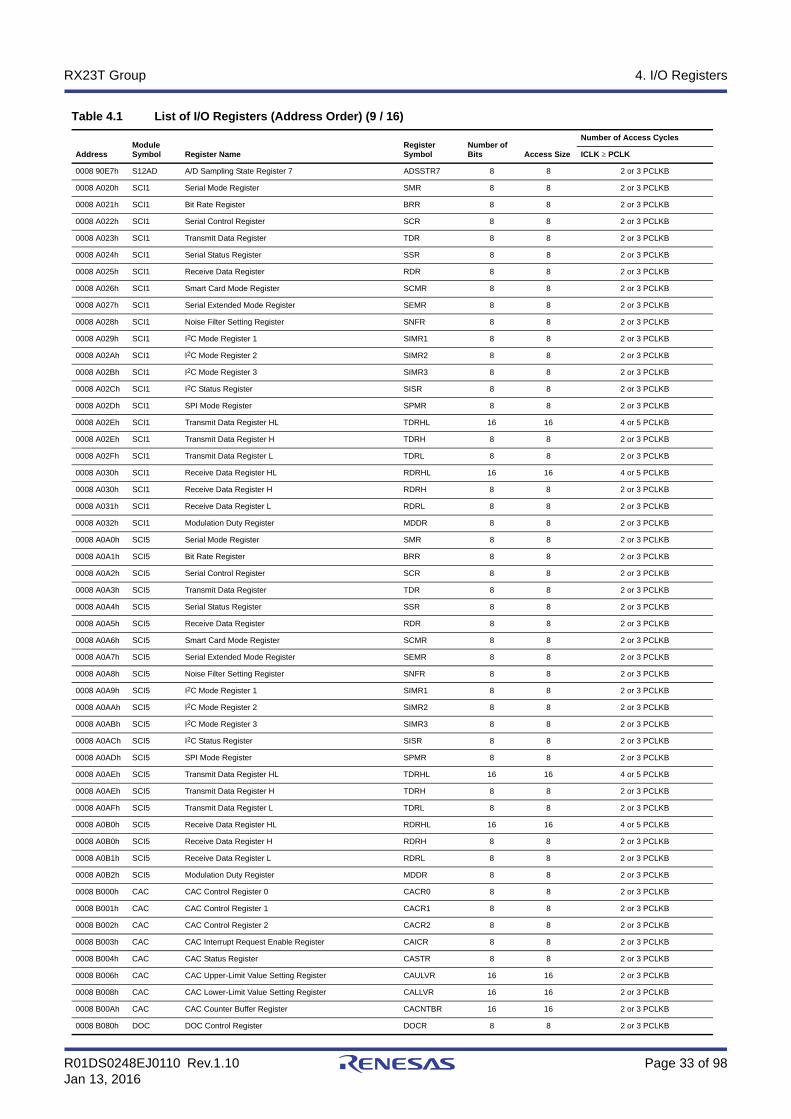
R01DS0248EJ0110 Rev.1.10 Page 33 of 98Jan 13, 2016
RX23T Group 4. I/O Registers
0008 90E7h S12AD A/D Sampling State Register 7 ADSSTR7 8 8 2 or 3 PCLKB
0008 A020h SCI1 Serial Mode Register SMR 8 8 2 or 3 PCLKB
0008 A021h SCI1 Bit Rate Register BRR 8 8 2 or 3 PCLKB
0008 A022h SCI1 Serial Control Register SCR 8 8 2 or 3 PCLKB
0008 A023h SCI1 Transmit Data Register TDR 8 8 2 or 3 PCLKB
0008 A024h SCI1 Serial Status Register SSR 8 8 2 or 3 PCLKB
0008 A025h SCI1 Receive Data Register RDR 8 8 2 or 3 PCLKB
0008 A026h SCI1 Smart Card Mode Register SCMR 8 8 2 or 3 PCLKB
0008 A027h SCI1 Serial Extended Mode Register SEMR 8 8 2 or 3 PCLKB
0008 A028h SCI1 Noise Filter Setting Register SNFR 8 8 2 or 3 PCLKB
0008 A029h SCI1 I2C Mode Register 1 SIMR1 8 8 2 or 3 PCLKB
0008 A02Ah SCI1 I2C Mode Register 2 SIMR2 8 8 2 or 3 PCLKB
0008 A02Bh SCI1 I2C Mode Register 3 SIMR3 8 8 2 or 3 PCLKB
0008 A02Ch SCI1 I2C Status Register SISR 8 8 2 or 3 PCLKB
0008 A02Dh SCI1 SPI Mode Register SPMR 8 8 2 or 3 PCLKB
0008 A02Eh SCI1 Transmit Data Register HL TDRHL 16 16 4 or 5 PCLKB
0008 A02Eh SCI1 Transmit Data Register H TDRH 8 8 2 or 3 PCLKB
0008 A02Fh SCI1 Transmit Data Register L TDRL 8 8 2 or 3 PCLKB
0008 A030h SCI1 Receive Data Register HL RDRHL 16 16 4 or 5 PCLKB
0008 A030h SCI1 Receive Data Register H RDRH 8 8 2 or 3 PCLKB
0008 A031h SCI1 Receive Data Register L RDRL 8 8 2 or 3 PCLKB
0008 A032h SCI1 Modulation Duty Register MDDR 8 8 2 or 3 PCLKB
0008 A0A0h SCI5 Serial Mode Register SMR 8 8 2 or 3 PCLKB
0008 A0A1h SCI5 Bit Rate Register BRR 8 8 2 or 3 PCLKB
0008 A0A2h SCI5 Serial Control Register SCR 8 8 2 or 3 PCLKB
0008 A0A3h SCI5 Transmit Data Register TDR 8 8 2 or 3 PCLKB
0008 A0A4h SCI5 Serial Status Register SSR 8 8 2 or 3 PCLKB
0008 A0A5h SCI5 Receive Data Register RDR 8 8 2 or 3 PCLKB
0008 A0A6h SCI5 Smart Card Mode Register SCMR 8 8 2 or 3 PCLKB
0008 A0A7h SCI5 Serial Extended Mode Register SEMR 8 8 2 or 3 PCLKB
0008 A0A8h SCI5 Noise Filter Setting Register SNFR 8 8 2 or 3 PCLKB
0008 A0A9h SCI5 I2C Mode Register 1 SIMR1 8 8 2 or 3 PCLKB
0008 A0AAh SCI5 I2C Mode Register 2 SIMR2 8 8 2 or 3 PCLKB
0008 A0ABh SCI5 I2C Mode Register 3 SIMR3 8 8 2 or 3 PCLKB
0008 A0ACh SCI5 I2C Status Register SISR 8 8 2 or 3 PCLKB
0008 A0ADh SCI5 SPI Mode Register SPMR 8 8 2 or 3 PCLKB
0008 A0AEh SCI5 Transmit Data Register HL TDRHL 16 16 4 or 5 PCLKB
0008 A0AEh SCI5 Transmit Data Register H TDRH 8 8 2 or 3 PCLKB
0008 A0AFh SCI5 Transmit Data Register L TDRL 8 8 2 or 3 PCLKB
0008 A0B0h SCI5 Receive Data Register HL RDRHL 16 16 4 or 5 PCLKB
0008 A0B0h SCI5 Receive Data Register H RDRH 8 8 2 or 3 PCLKB
0008 A0B1h SCI5 Receive Data Register L RDRL 8 8 2 or 3 PCLKB
0008 A0B2h SCI5 Modulation Duty Register MDDR 8 8 2 or 3 PCLKB
0008 B000h CAC CAC Control Register 0 CACR0 8 8 2 or 3 PCLKB
0008 B001h CAC CAC Control Register 1 CACR1 8 8 2 or 3 PCLKB
0008 B002h CAC CAC Control Register 2 CACR2 8 8 2 or 3 PCLKB
0008 B003h CAC CAC Interrupt Request Enable Register CAICR 8 8 2 or 3 PCLKB
0008 B004h CAC CAC Status Register CASTR 8 8 2 or 3 PCLKB
0008 B006h CAC CAC Upper-Limit Value Setting Register CAULVR 16 16 2 or 3 PCLKB
0008 B008h CAC CAC Lower-Limit Value Setting Register CALLVR 16 16 2 or 3 PCLKB
0008 B00Ah CAC CAC Counter Buffer Register CACNTBR 16 16 2 or 3 PCLKB
0008 B080h DOC DOC Control Register DOCR 8 8 2 or 3 PCLKB
Table 4.1 List of I/O Registers (Address Order) (9 / 16)
AddressModule Symbol Register Name
Register Symbol
Number of Bits Access Size
Number of Access Cycles
ICLK PCLK

R01DS0248EJ0110 Rev.1.10 Page 34 of 98Jan 13, 2016
RX23T Group 4. I/O Registers
0008 B082h DOC DOC Data Input Register DODIR 16 16 2 or 3 PCLKB
0008 B084h DOC DOC Data Setting Register DODSR 16 16 2 or 3 PCLKB
0008 C000h PORT0 Port Direction Register PDR 8 8 2 or 3 PCLKB
0008 C001h PORT1 Port Direction Register PDR 8 8 2 or 3 PCLKB
0008 C002h PORT2 Port Direction Register PDR 8 8 2 or 3 PCLKB
0008 C003h PORT3 Port Direction Register PDR 8 8 2 or 3 PCLKB
0008 C004h PORT4 Port Direction Register PDR 8 8 2 or 3 PCLKB
0008 C007h PORT7 Port Direction Register PDR 8 8 2 or 3 PCLKB
0008 C009h PORT9 Port Direction Register PDR 8 8 2 or 3 PCLKB
0008 C00Ah PORTA Port Direction Register PDR 8 8 2 or 3 PCLKB
0008 C00Bh PORTB Port Direction Register PDR 8 8 2 or 3 PCLKB
0008 C00Dh PORTD Port Direction Register PDR 8 8 2 or 3 PCLKB
0008 C020h PORT0 Port Output Data Register PODR 8 8 2 or 3 PCLKB
0008 C021h PORT1 Port Output Data Register PODR 8 8 2 or 3 PCLKB
0008 C022h PORT2 Port Output Data Register PODR 8 8 2 or 3 PCLKB
0008 C023h PORT3 Port Output Data Register PODR 8 8 2 or 3 PCLKB
0008 C024h PORT4 Port Output Data Register PODR 8 8 2 or 3 PCLKB
0008 C027h PORT7 Port Output Data Register PODR 8 8 2 or 3 PCLKB
0008 C029h PORT9 Port Output Data Register PODR 8 8 2 or 3 PCLKB
0008 C02Ah PORTA Port Output Data Register PODR 8 8 2 or 3 PCLKB
0008 C02Bh PORTB Port Output Data Register PODR 8 8 2 or 3 PCLKB
0008 C02Dh PORTD Port Output Data Register PODR 8 8 2 or 3 PCLKB
0008 C040h PORT0 Port Input Data Register PIDR 8 8 2 or 3 PCLKB
0008 C041h PORT1 Port Input Data Register PIDR 8 8 2 or 3 PCLKB
0008 C042h PORT2 Port Input Data Register PIDR 8 8 2 or 3 PCLKB
0008 C043h PORT3 Port Input Data Register PIDR 8 8 2 or 3 PCLKB
0008 C044h PORT4 Port Input Data Register PIDR 8 8 2 or 3 PCLKB
0008 C047h PORT7 Port Input Data Register PIDR 8 8 2 or 3 PCLKB
0008 C049h PORT9 Port Input Data Register PIDR 8 8 2 or 3 PCLKB
0008 C04Ah PORTA Port Input Data Register PIDR 8 8 2 or 3 PCLKB
0008 C04Bh PORTB Port Input Data Register PIDR 8 8 2 or 3 PCLKB
0008 C04Dh PORTD Port Input Data Register PIDR 8 8 2 or 3 PCLKB
0008 C04Eh PORTE Port Input Data Register PIDR 8 8 2 or 3 PCLKB
0008 C060h PORT0 Port Mode Register PMR 8 8 2 or 3 PCLKB
0008 C061h PORT1 Port Mode Register PMR 8 8 2 or 3 PCLKB
0008 C062h PORT2 Port Mode Register PMR 8 8 2 or 3 PCLKB
0008 C063h PORT3 Port Mode Register PMR 8 8 2 or 3 PCLKB
0008 C067h PORT7 Port Mode Register PMR 8 8 2 or 3 PCLKB
0008 C069h PORT9 Port Mode Register PMR 8 8 2 or 3 PCLKB
0008 C06Ah PORTA Port Mode Register PMR 8 8 2 or 3 PCLKB
0008 C06Bh PORTB Port Mode Register PMR 8 8 2 or 3 PCLKB
0008 C06Dh PORTD Port Mode Register PMR 8 8 2 or 3 PCLKB
0008 C06Eh PORTE Port Mode Register PMR 8 8 2 or 3 PCLKB
0008 C080h PORT0 Open Drain Control Register 0 ODR0 8 8, 16 2 or 3 PCLKB
0008 C082h PORT1 Open Drain Control Register 0 ODR0 8 8, 16 2 or 3 PCLKB
0008 C084h PORT2 Open Drain Control Register 0 ODR0 8 8, 16 2 or 3 PCLKB
0008 C085h PORT2 Open Drain Control Register 1 ODR1 8 8, 16 2 or 3 PCLKB
0008 C086h PORT3 Open Drain Control Register 0 ODR0 8 8, 16 2 or 3 PCLKB
0008 C087h PORT3 Open Drain Control Register 1 ODR1 8 8, 16 2 or 3 PCLKB
0008 C08Eh PORT7 Open Drain Control Register 0 ODR0 8 8, 16 2 or 3 PCLKB
0008 C08Fh PORT7 Open Drain Control Register 1 ODR1 8 8, 16 2 or 3 PCLKB
0008 C092h PORT9 Open Drain Control Register 0 ODR0 8 8, 16 2 or 3 PCLKB
Table 4.1 List of I/O Registers (Address Order) (10 / 16)
AddressModule Symbol Register Name
Register Symbol
Number of Bits Access Size
Number of Access Cycles
ICLK PCLK
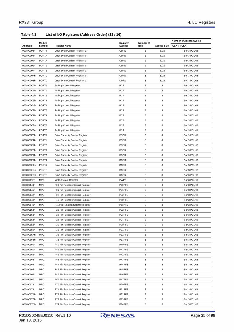
R01DS0248EJ0110 Rev.1.10 Page 35 of 98Jan 13, 2016
RX23T Group 4. I/O Registers
0008 C093h PORT9 Open Drain Control Register 1 ODR1 8 8, 16 2 or 3 PCLKB
0008 C094h PORTA Open Drain Control Register 0 ODR0 8 8, 16 2 or 3 PCLKB
0008 C095h PORTA Open Drain Control Register 1 ODR1 8 8, 16 2 or 3 PCLKB
0008 C096h PORTB Open Drain Control Register 0 ODR0 8 8, 16 2 or 3 PCLKB
0008 C097h PORTB Open Drain Control Register 1 ODR1 8 8, 16 2 or 3 PCLKB
0008 C09Ah PORTD Open Drain Control Register 0 ODR0 8 8, 16 2 or 3 PCLKB
0008 C09Bh PORTD Open Drain Control Register 1 ODR1 8 8, 16 2 or 3 PCLKB
0008 C0C0h PORT0 Pull-Up Control Register PCR 8 8 2 or 3 PCLKB
0008 C0C1h PORT1 Pull-Up Control Register PCR 8 8 2 or 3 PCLKB
0008 C0C2h PORT2 Pull-Up Control Register PCR 8 8 2 or 3 PCLKB
0008 C0C3h PORT3 Pull-Up Control Register PCR 8 8 2 or 3 PCLKB
0008 C0C4h PORT4 Pull-Up Control Register PCR 8 8 2 or 3 PCLKB
0008 C0C7h PORT7 Pull-Up Control Register PCR 8 8 2 or 3 PCLKB
0008 C0C9h PORT9 Pull-Up Control Register PCR 8 8 2 or 3 PCLKB
0008 C0CAh PORTA Pull-Up Control Register PCR 8 8 2 or 3 PCLKB
0008 C0CBh PORTB Pull-Up Control Register PCR 8 8 2 or 3 PCLKB
0008 C0CDh PORTD Pull-Up Control Register PCR 8 8 2 or 3 PCLKB
0008 C0E0h PORT0 Drive Capacity Control Register DSCR 8 8 2 or 3 PCLKB
0008 C0E1h PORT1 Drive Capacity Control Register DSCR 8 8 2 or 3 PCLKB
0008 C0E2h PORT2 Drive Capacity Control Register DSCR 8 8 2 or 3 PCLKB
0008 C0E3h PORT3 Drive Capacity Control Register DSCR 8 8 2 or 3 PCLKB
0008 C0E7h PORT7 Drive Capacity Control Register DSCR 8 8 2 or 3 PCLKB
0008 C0E9h PORT9 Drive Capacity Control Register DSCR 8 8 2 or 3 PCLKB
0008 C0EAh PORTA Drive Capacity Control Register DSCR 8 8 2 or 3 PCLKB
0008 C0EBh PORTB Drive Capacity Control Register DSCR 8 8 2 or 3 PCLKB
0008 C0EDh PORTD Drive Capacity Control Register DSCR 8 8 2 or 3 PCLKB
0008 C11Fh MPC Write-Protect Register PWPR 8 8 2 or 3 PCLKB
0008 C140h MPC P00 Pin Function Control Register P00PFS 8 8 2 or 3 PCLKB
0008 C141h MPC P01 Pin Function Control Register P01PFS 8 8 2 or 3 PCLKB
0008 C142h MPC P02 Pin Function Control Register P02PFS 8 8 2 or 3 PCLKB
0008 C148h MPC P10 Pin Function Control Register P10PFS 8 8 2 or 3 PCLKB
0008 C149h MPC P11 Pin Function Control Register P11PFS 8 8 2 or 3 PCLKB
0008 C152h MPC P22 Pin Function Control Register P22PFS 8 8 2 or 3 PCLKB
0008 C153h MPC P23 Pin Function Control Register P23PFS 8 8 2 or 3 PCLKB
0008 C154h MPC P24 Pin Function Control Register P24PFS 8 8 2 or 3 PCLKB
0008 C158h MPC P30 Pin Function Control Register P30PFS 8 8 2 or 3 PCLKB
0008 C159h MPC P31 Pin Function Control Register P31PFS 8 8 2 or 3 PCLKB
0008 C15Ah MPC P32 Pin Function Control Register P32PFS 8 8 2 or 3 PCLKB
0008 C15Bh MPC P33 Pin Function Control Register P33PFS 8 8 2 or 3 PCLKB
0008 C160h MPC P40 Pin Function Control Register P40PFS 8 8 2 or 3 PCLKB
0008 C161h MPC P41 Pin Function Control Register P41PFS 8 8 2 or 3 PCLKB
0008 C162h MPC P42 Pin Function Control Register P42PFS 8 8 2 or 3 PCLKB
0008 C163h MPC P43 Pin Function Control Register P43PFS 8 8 2 or 3 PCLKB
0008 C164h MPC P44 Pin Function Control Register P44PFS 8 8 2 or 3 PCLKB
0008 C165h MPC P45 Pin Function Control Register P45PFS 8 8 2 or 3 PCLKB
0008 C166h MPC P46 Pin Function Control Register P46PFS 8 8 2 or 3 PCLKB
0008 C167h MPC P47 Pin Function Control Register P47PFS 8 8 2 or 3 PCLKB
0008 C178h MPC P70 Pin Function Control Register P70PFS 8 8 2 or 3 PCLKB
0008 C179h MPC P71 Pin Function Control Register P71PFS 8 8 2 or 3 PCLKB
0008 C17Ah MPC P72 Pin Function Control Register P72PFS 8 8 2 or 3 PCLKB
0008 C17Bh MPC P73 Pin Function Control Register P73PFS 8 8 2 or 3 PCLKB
0008 C17Ch MPC P74 Pin Function Control Register P74PFS 8 8 2 or 3 PCLKB
Table 4.1 List of I/O Registers (Address Order) (11 / 16)
AddressModule Symbol Register Name
Register Symbol
Number of Bits Access Size
Number of Access Cycles
ICLK PCLK
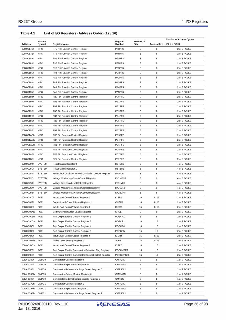
R01DS0248EJ0110 Rev.1.10 Page 36 of 98Jan 13, 2016
RX23T Group 4. I/O Registers
0008 C17Dh MPC P75 Pin Function Control Register P75PFS 8 8 2 or 3 PCLKB
0008 C17Eh MPC P76 Pin Function Control Register P76PFS 8 8 2 or 3 PCLKB
0008 C189h MPC P91 Pin Function Control Register P91PFS 8 8 2 or 3 PCLKB
0008 C18Ah MPC P92 Pin Function Control Register P92PFS 8 8 2 or 3 PCLKB
0008 C18Bh MPC P93 Pin Function Control Register P93PFS 8 8 2 or 3 PCLKB
0008 C18Ch MPC P94 Pin Function Control Register P94PFS 8 8 2 or 3 PCLKB
0008 C192h MPC PA2 Pin Function Control Register PA2PFS 8 8 2 or 3 PCLKB
0008 C193h MPC PA3 Pin Function Control Register PA3PFS 8 8 2 or 3 PCLKB
0008 C194h MPC PA4 Pin Function Control Register PA4PFS 8 8 2 or 3 PCLKB
0008 C195h MPC PA5 Pin Function Control Register PA5PFS 8 8 2 or 3 PCLKB
0008 C198h MPC PB0 Pin Function Control Register PB0PFS 8 8 2 or 3 PCLKB
0008 C199h MPC PB1 Pin Function Control Register PB1PFS 8 8 2 or 3 PCLKB
0008 C19Ah MPC PB2 Pin Function Control Register PB2PFS 8 8 2 or 3 PCLKB
0008 C19Bh MPC PB3 Pin Function Control Register PB3PFS 8 8 2 or 3 PCLKB
0008 C19Ch MPC PB4 Pin Function Control Register PB4PFS 8 8 2 or 3 PCLKB
0008 C19Dh MPC PB5 Pin Function Control Register PB5PFS 8 8 2 or 3 PCLKB
0008 C19Eh MPC PB6 Pin Function Control Register PB6PFS 8 8 2 or 3 PCLKB
0008 C19Fh MPC PB7 Pin Function Control Register PB7PFS 8 8 2 or 3 PCLKB
0008 C1ABh MPC PD3 Pin Function Control Register PD3PFS 8 8 2 or 3 PCLKB
0008 C1ACh MPC PD4 Pin Function Control Register PD4PFS 8 8 2 or 3 PCLKB
0008 C1ADh MPC PD5 Pin Function Control Register PD5PFS 8 8 2 or 3 PCLKB
0008 C1AEh MPC PD6 Pin Function Control Register PD6PFS 8 8 2 or 3 PCLKB
0008 C1AFh MPC PD7 Pin Function Control Register PD7PFS 8 8 2 or 3 PCLKB
0008 C1B2h MPC PE2 Pin Function Control Register PE2PFS 8 8 2 or 3 PCLKB
0008 C290h SYSTEM Reset Status Register 0 RSTSR0 8 8 4 or 5 PCLKB
0008 C291h SYSTEM Reset Status Register 1 RSTSR1 8 8 4 or 5 PCLKB
0008 C293h SYSTEM Main Clock Oscillator Forced Oscillation Control Register MOFCR 8 8 4 or 5 PCLKB
0008 C297h SYSTEM Voltage Monitoring Circuit Control Register LVCMPCR 8 8 4 or 5 PCLKB
0008 C298h SYSTEM Voltage Detection Level Select Register LVDLVLR 8 8 4 or 5 PCLKB
0008 C29Ah SYSTEM Voltage Monitoring 1 Circuit Control Register 0 LVD1CR0 8 8 4 or 5 PCLKB
0008 C29Bh SYSTEM Voltage Monitoring 2 Circuit Control Register 0 LVD2CR0 8 8 4 or 5 PCLKB
0008 C4C0h POE Input Level Control/Status Register 1 ICSR1 16 8, 16 2 or 3 PCLKB
0008 C4C2h POE Output Level Control/Status Register 1 OCSR1 16 8, 16 2 or 3 PCLKB
0008 C4C8h POE Input Level Control/Status Register 3 ICSR3 16 8, 16 2 or 3 PCLKB
0008 C4CAh POE Software Port Output Enable Register SPOER 8 8 2 or 3 PCLKB
0008 C4CBh POE Port Output Enable Control Register 1 POECR1 8 8 2 or 3 PCLKB
0008 C4CCh POE Port Output Enable Control Register 2 POECR2 16 16 2 or 3 PCLKB
0008 C4D0h POE Port Output Enable Control Register 4 POECR4 16 16 2 or 3 PCLKB
0008 C4D2h POE Port Output Enable Control Register 5 POECR5 16 16 2 or 3 PCLKB
0008 C4D6h POE Input Level Control/Status Register 4 ICSR4 16 8, 16 2 or 3 PCLKB
0008 C4DAh POE Active Level Setting Register 1 ALR1 16 8, 16 2 or 3 PCLKB
0008 C4DCh POE Input Level Control/Status Register 6 ICSR6 16 16 2 or 3 PCLKB
0008 C4E6h POE Port Output Enable Comparator Detection Flag Register POECMPFR 16 16 2 or 3 PCLKB
0008 C4E8h POE Port Output Enable Comparator Request Select Register POECMPSEL 16 16 2 or 3 PCLKB
000A 0C80h CMPC0 Comparator Control Register 0 CMPCTL 8 8 1 or 2 PCLKB
000A 0C84h CMPC0 Comparator Input Select Register 0 CMPSEL0 8 8 1 or 2 PCLKB
000A 0C88h CMPC0 Comparator Reference Voltage Select Register 0 CMPSEL1 8 8 1 or 2 PCLKB
000A 0C8Ch CMPC0 Comparator Output Monitor Register 0 CMPMON 8 8 1 or 2 PCLKB
000A 0C90h CMPC0 Comparator External Output Enable Register 0 CMPIOC 8 8 1 or 2 PCLKB
000A 0CA0h CMPC1 Comparator Control Register 1 CMPCTL 8 8 1 or 2 PCLKB
000A 0CA4h CMPC1 Comparator Input Select Register 1 CMPSEL0 8 8 1 or 2 PCLKB
000A 0CA8h CMPC1 Comparator Reference Voltage Select Register 1 CMPSEL1 8 8 1 or 2 PCLKB
Table 4.1 List of I/O Registers (Address Order) (12 / 16)
AddressModule Symbol Register Name
Register Symbol
Number of Bits Access Size
Number of Access Cycles
ICLK PCLK

R01DS0248EJ0110 Rev.1.10 Page 37 of 98Jan 13, 2016
RX23T Group 4. I/O Registers
000A 0CACh CMPC1 Comparator Output Monitor Register 1 CMPMON 8 8 1 or 2 PCLKB
000A 0CB0h CMPC1 Comparator External Output Enable Register 1 CMPIOC 8 8 1 or 2 PCLKB
000A 0CC0h CMPC2 Comparator Control Register 2 CMPCTL 8 8 1 or 2 PCLKB
000A 0CC4h CMPC2 Comparator Input Select Register 2 CMPSEL0 8 8 1 or 2 PCLKB
000A 0CC8h CMPC2 Comparator Reference Voltage Select Register 2 CMPSEL1 8 8 1 or 2 PCLKB
000A 0CCCh CMPC2 Comparator Output Monitor Register 2 CMPMON 8 8 1 or 2 PCLKB
000A 0CD0h CMPC2 Comparator External Output Enable Register 2 CMPIOC 8 8 1 or 2 PCLKB
000C 1200h MTU3 Timer Control Register TCR 8 8, 16, 32 4 or 5 PCLKA
000C 1201h MTU4 Timer Control Register TCR 8 8 4 or 5 PCLKA
000C 1202h MTU3 Timer Mode Register 1 TMDR1 8 8, 16 4 or 5 PCLKA
000C 1203h MTU4 Timer Mode Register 1 TMDR1 8 8 4 or 5 PCLKA
000C 1204h MTU3 Timer I/O Control Register H TIORH 8 8, 16, 32 4 or 5 PCLKA
000C 1205h MTU3 Timer I/O Control Register L TIORL 8 8 4 or 5 PCLKA
000C 1206h MTU4 Timer I/O Control Register H TIORH 8 8, 16 4 or 5 PCLKA
000C 1207h MTU4 Timer I/O Control Register L TIORL 8 8 4 or 5 PCLKA
000C 1208h MTU3 Timer Interrupt Enable Register TIER 8 8, 16 4 or 5 PCLKA
000C 1209h MTU4 Timer Interrupt Enable Register TIER 8 8 4 or 5 PCLKA
000C 120Ah MTU Timer Output Master Enable Register A TOERA 8 8 4 or 5 PCLKA
000C 120Dh MTU Timer Gate Control Register TGCRA 8 8 4 or 5 PCLKA
000C 120Eh MTU Timer Output Control Register 1A TOCR1A 8 8, 16 4 or 5 PCLKA
000C 120Fh MTU Timer Output Control Register 2A TOCR2A 8 8 4 or 5 PCLKA
000C 1210h MTU3 Timer Counter TCNT 16 16, 32 4 or 5 PCLKA
000C 1212h MTU4 Timer Counter TCNT 16 16 4 or 5 PCLKA
000C 1214h MTU Timer Cycle Data Register A TCDRA 16 16, 32 4 or 5 PCLKA
000C 1216h MTU Timer Dead Time Data Register A TDDRA 16 16 4 or 5 PCLKA
000C 1218h MTU3 Timer General Register A TGRA 16 16, 32 4 or 5 PCLKA
000C 121Ah MTU3 Timer General Register B TGRB 16 16 4 or 5 PCLKA
000C 121Ch MTU4 Timer General Register A TGRA 16 16, 32 4 or 5 PCLKA
000C 121Eh MTU4 Timer General Register B TGRB 16 16 4 or 5 PCLKA
000C 1220h MTU Timer Subcounters A TCNTSA 16 16, 32 4 or 5 PCLKA
000C 1222h MTU Timer Cycle Buffer Register A TCBRA 16 16 4 or 5 PCLKA
000C 1224h MTU3 Timer General Register C TGRC 16 16, 32 4 or 5 PCLKA
000C 1226h MTU3 Timer General Register D TGRD 16 16 4 or 5 PCLKA
000C 1228h MTU4 Timer General Register C TGRC 16 16, 32 4 or 5 PCLKA
000C 122Ah MTU4 Timer General Register D TGRD 16 16 4 or 5 PCLKA
000C 122Ch MTU3 Timer Status Register TSR 8 8, 16 4 or 5 PCLKA
000C 122Dh MTU4 Timer Status Register TSR 8 8 4 or 5 PCLKA
000C 1230h MTU Timer Interrupt Skipping Set Register 1A TITCR1A 8 8, 16 4 or 5 PCLKA
000C 1231h MTU Timer Interrupt Skipping Counters 1A TITCNT1A 8 8 4 or 5 PCLKA
000C 1232h MTU Timer Buffer Transfer Set Register A TBTERA 8 8 4 or 5 PCLKA
000C 1234h MTU Timer Dead Time Enable Register A TDERA 8 8 4 or 5 PCLKA
000C 1236h MTU Timer Output Level Buffer Register A TOLBRA 8 8 4 or 5 PCLKA
000C 1238h MTU3 Timer Buffer Operation Transfer Mode Register TBTM 8 8, 16 4 or 5 PCLKA
000C 1239h MTU4 Timer Buffer Operation Transfer Mode Register TBTM 8 8 4 or 5 PCLKA
000C 123Ah MTU Timer Interrupt Skipping Mode Register A TITMRA 8 8 4 or 5 PCLKA
000C 123Bh MTU Timer Interrupt Skipping Set Register 2A TITCR2A 8 8 4 or 5 PCLKA
000C 123Ch MTU Timer Interrupt Skipping Counters 2A TITCNT2A 8 8 4 or 5 PCLKA
000C 1240h MTU4 Timer A/D Converter Start Request Control Register TADCR 16 16 4 or 5 PCLKA
000C 1244h MTU4 Timer A/D Converter Start Request Cycle Set Register A TADCORA 16 16, 32 4 or 5 PCLKA
000C 1246h MTU4 Timer A/D Converter Start Request Cycle Set Register B TADCORB 16 16 4 or 5 PCLKA
000C 1248h MTU4 Timer A/D Converter Start Request Cycle Set Buffer Register A
TADCOBRA16 16, 32 4 or 5 PCLKA
Table 4.1 List of I/O Registers (Address Order) (13 / 16)
AddressModule Symbol Register Name
Register Symbol
Number of Bits Access Size
Number of Access Cycles
ICLK PCLK
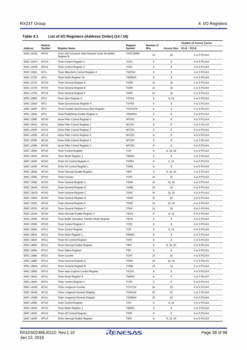
R01DS0248EJ0110 Rev.1.10 Page 38 of 98Jan 13, 2016
RX23T Group 4. I/O Registers
000C 124Ah MTU4 Timer A/D Converter Start Request Cycle Set Buffer Register B
TADCOBRB16 16 4 or 5 PCLKA
000C 124Ch MTU3 Timer Control Register 2 TCR2 8 8 4 or 5 PCLKA
000C 124Dh MTU4 Timer Control Register 2 TCR2 8 8 4 or 5 PCLKA
000C 1260h MTU Timer Waveform Control Register A TWCRA 8 8 4 or 5 PCLKA
000C 1270h MTU Timer Mode Register 2A TMDR2A 8 8 4 or 5 PCLKA
000C 1272h MTU3 Timer General Register E TGRE 16 16 4 or 5 PCLKA
000C 1274h MTU4 Timer General Register E TGRE 16 16 4 or 5 PCLKA
000C 1276h MTU4 Timer General Register F TGRF 16 16 4 or 5 PCLKA
000C 1280h MTU Timer Start Register A TSTRA 8 8, 16 4 or 5 PCLKA
000C 1281h MTU Timer Synchronous Register A TSYRA 8 8 4 or 5 PCLKA
000C 1282h MTU Timer Counter Synchronous Start Register TCSYSTR 8 8 4 or 5 PCLKA
000C 1284h MTU Timer Read/Write Enable Register A TRWERA 8 8 4 or 5 PCLKA
000C 1290h MTU0 Noise Filter Control Register 0 NFCR0 8 8 4 or 5 PCLKA
000C 1291h MTU1 Noise Filter Control Register 1 NFCR1 8 8 4 or 5 PCLKA
000C 1292h MTU2 Noise Filter Control Register 2 NFCR2 8 8 4 or 5 PCLKA
000C 1293h MTU3 Noise Filter Control Register 3 NFCR3 8 8 4 or 5 PCLKA
000C 1294h MTU4 Noise Filter Control Register 4 NFCR4 8 8 4 or 5 PCLKA
000C 1299h MTU0 Noise Filter Control Register C NFCRC 8 8 4 or 5 PCLKA
000C 1300h MTU0 Timer Control Register TCR 8 8, 16, 32 4 or 5 PCLKA
000C 1301h MTU0 Timer Mode Register 1 TMDR1 8 8 4 or 5 PCLKA
000C 1302h MTU0 Timer I/O Control Register H TIORH 8 8, 16 4 or 5 PCLKA
000C 1303h MTU0 Timer I/O Control Register L TIORL 8 8 4 or 5 PCLKA
000C 1304h MTU0 Timer Interrupt Enable Register TIER 8 8, 16, 32 4 or 5 PCLKA
000C 1306h MTU0 Timer Counter TCNT 16 16 4 or 5 PCLKA
000C 1308h MTU0 Timer General Register A TGRA 16 16, 32 4 or 5 PCLKA
000C 130Ah MTU0 Timer General Register B TGRB 16 16 4 or 5 PCLKA
000C 130Ch MTU0 Timer General Register C TGRC 16 16, 32 4 or 5 PCLKA
000C 130Eh MTU0 Timer General Register D TGRD 16 16 4 or 5 PCLKA
000C 1320h MTU0 Timer General Register E TGRE 16 16, 32 4 or 5 PCLKA
000C 1322h MTU0 Timer General Register F TGRF 16 16 4 or 5 PCLKA
000C 1324h MTU0 Timer Interrupt Enable Register 2 TIER2 8 8, 16 4 or 5 PCLKA
000C 1326h MTU0 Timer Buffer Operation Transfer Mode Register TBTM 8 8 4 or 5 PCLKA
000C 1328h MTU0 Timer Control Register 2 TCR2 8 8 4 or 5 PCLKA
000C 1380h MTU1 Timer Control Register TCR 8 8, 16 4 or 5 PCLKA
000C 1381h MTU1 Timer Mode Register 1 TMDR1 8 8 4 or 5 PCLKA
000C 1382h MTU1 Timer I/O Control Register TIOR 8 8 4 or 5 PCLKA
000C 1384h MTU1 Timer Interrupt Enable Register TIER 8 8, 16, 32 4 or 5 PCLKA
000C 1385h MTU1 Timer Status Register TSR 8 8 4 or 5 PCLKA
000C 1386h MTU1 Timer Counter TCNT 16 16 4 or 5 PCLKA
000C 1388h MTU1 Timer General Register A TGRA 16 16, 32 4 or 5 PCLKA
000C 138Ah MTU1 Timer General Register B TGRB 16 16 4 or 5 PCLKA
000C 1390h MTU1 Timer Input Capture Control Register TICCR 8 8 4 or 5 PCLKA
000C 1391h MTU1 Timer Mode Register 3 TMDR3 8 8 4 or 5 PCLKA
000C 1394h MTU1 Timer Control Register 2 TCR2 8 8 4 or 5 PCLKA
000C 13A0h MTU1 Timer Longword Counter TCNTLW 32 32 4 or 5 PCLKA
000C 13A4h MTU1 Timer Longword General Register TGRALW 32 32 4 or 5 PCLKA
000C 13A8h MTU1 Timer Longword General Register TGRBLW 32 32 4 or 5 PCLKA
000C 1400h MTU2 Timer Control Register TCR 8 8, 16 4 or 5 PCLKA
000C 1401h MTU2 Timer Mode Register 1 TMDR1 8 8 4 or 5 PCLKA
000C 1402h MTU2 Timer I/O Control Register TIOR 8 8 4 or 5 PCLKA
000C 1404h MTU2 Timer Interrupt Enable Register TIER 8 8, 16, 32 4 or 5 PCLKA
Table 4.1 List of I/O Registers (Address Order) (14 / 16)
AddressModule Symbol Register Name
Register Symbol
Number of Bits Access Size
Number of Access Cycles
ICLK PCLK
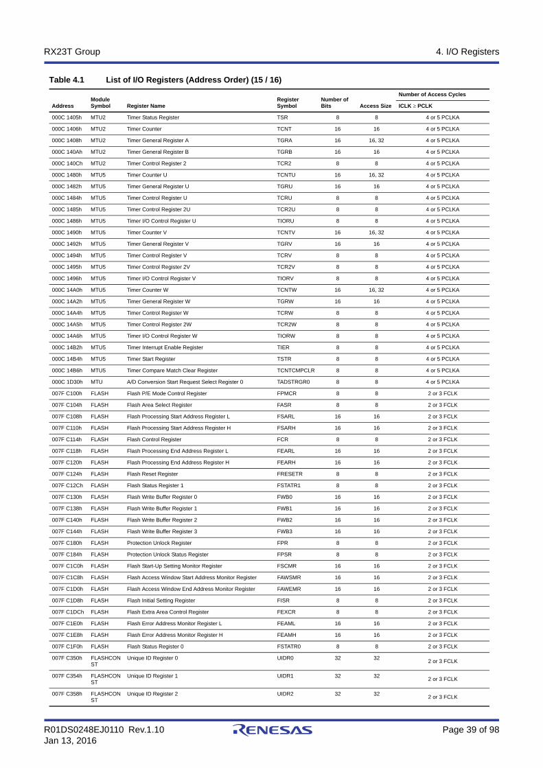
R01DS0248EJ0110 Rev.1.10 Page 39 of 98Jan 13, 2016
RX23T Group 4. I/O Registers
000C 1405h MTU2 Timer Status Register TSR 8 8 4 or 5 PCLKA
000C 1406h MTU2 Timer Counter TCNT 16 16 4 or 5 PCLKA
000C 1408h MTU2 Timer General Register A TGRA 16 16, 32 4 or 5 PCLKA
000C 140Ah MTU2 Timer General Register B TGRB 16 16 4 or 5 PCLKA
000C 140Ch MTU2 Timer Control Register 2 TCR2 8 8 4 or 5 PCLKA
000C 1480h MTU5 Timer Counter U TCNTU 16 16, 32 4 or 5 PCLKA
000C 1482h MTU5 Timer General Register U TGRU 16 16 4 or 5 PCLKA
000C 1484h MTU5 Timer Control Register U TCRU 8 8 4 or 5 PCLKA
000C 1485h MTU5 Timer Control Register 2U TCR2U 8 8 4 or 5 PCLKA
000C 1486h MTU5 Timer I/O Control Register U TIORU 8 8 4 or 5 PCLKA
000C 1490h MTU5 Timer Counter V TCNTV 16 16, 32 4 or 5 PCLKA
000C 1492h MTU5 Timer General Register V TGRV 16 16 4 or 5 PCLKA
000C 1494h MTU5 Timer Control Register V TCRV 8 8 4 or 5 PCLKA
000C 1495h MTU5 Timer Control Register 2V TCR2V 8 8 4 or 5 PCLKA
000C 1496h MTU5 Timer I/O Control Register V TIORV 8 8 4 or 5 PCLKA
000C 14A0h MTU5 Timer Counter W TCNTW 16 16, 32 4 or 5 PCLKA
000C 14A2h MTU5 Timer General Register W TGRW 16 16 4 or 5 PCLKA
000C 14A4h MTU5 Timer Control Register W TCRW 8 8 4 or 5 PCLKA
000C 14A5h MTU5 Timer Control Register 2W TCR2W 8 8 4 or 5 PCLKA
000C 14A6h MTU5 Timer I/O Control Register W TIORW 8 8 4 or 5 PCLKA
000C 14B2h MTU5 Timer Interrupt Enable Register TIER 8 8 4 or 5 PCLKA
000C 14B4h MTU5 Timer Start Register TSTR 8 8 4 or 5 PCLKA
000C 14B6h MTU5 Timer Compare Match Clear Register TCNTCMPCLR 8 8 4 or 5 PCLKA
000C 1D30h MTU A/D Conversion Start Request Select Register 0 TADSTRGR0 8 8 4 or 5 PCLKA
007F C100h FLASH Flash P/E Mode Control Register FPMCR 8 8 2 or 3 FCLK
007F C104h FLASH Flash Area Select Register FASR 8 8 2 or 3 FCLK
007F C108h FLASH Flash Processing Start Address Register L FSARL 16 16 2 or 3 FCLK
007F C110h FLASH Flash Processing Start Address Register H FSARH 16 16 2 or 3 FCLK
007F C114h FLASH Flash Control Register FCR 8 8 2 or 3 FCLK
007F C118h FLASH Flash Processing End Address Register L FEARL 16 16 2 or 3 FCLK
007F C120h FLASH Flash Processing End Address Register H FEARH 16 16 2 or 3 FCLK
007F C124h FLASH Flash Reset Register FRESETR 8 8 2 or 3 FCLK
007F C12Ch FLASH Flash Status Register 1 FSTATR1 8 8 2 or 3 FCLK
007F C130h FLASH Flash Write Buffer Register 0 FWB0 16 16 2 or 3 FCLK
007F C138h FLASH Flash Write Buffer Register 1 FWB1 16 16 2 or 3 FCLK
007F C140h FLASH Flash Write Buffer Register 2 FWB2 16 16 2 or 3 FCLK
007F C144h FLASH Flash Write Buffer Register 3 FWB3 16 16 2 or 3 FCLK
007F C180h FLASH Protection Unlock Register FPR 8 8 2 or 3 FCLK
007F C184h FLASH Protection Unlock Status Register FPSR 8 8 2 or 3 FCLK
007F C1C0h FLASH Flash Start-Up Setting Monitor Register FSCMR 16 16 2 or 3 FCLK
007F C1C8h FLASH Flash Access Window Start Address Monitor Register FAWSMR 16 16 2 or 3 FCLK
007F C1D0h FLASH Flash Access Window End Address Monitor Register FAWEMR 16 16 2 or 3 FCLK
007F C1D8h FLASH Flash Initial Setting Register FISR 8 8 2 or 3 FCLK
007F C1DCh FLASH Flash Extra Area Control Register FEXCR 8 8 2 or 3 FCLK
007F C1E0h FLASH Flash Error Address Monitor Register L FEAML 16 16 2 or 3 FCLK
007F C1E8h FLASH Flash Error Address Monitor Register H FEAMH 16 16 2 or 3 FCLK
007F C1F0h FLASH Flash Status Register 0 FSTATR0 8 8 2 or 3 FCLK
007F C350h FLASHCONST
Unique ID Register 0 UIDR0 32 322 or 3 FCLK
007F C354h FLASHCONST
Unique ID Register 1 UIDR1 32 322 or 3 FCLK
007F C358h FLASHCONST
Unique ID Register 2 UIDR2 32 322 or 3 FCLK
Table 4.1 List of I/O Registers (Address Order) (15 / 16)
AddressModule Symbol Register Name
Register Symbol
Number of Bits Access Size
Number of Access Cycles
ICLK PCLK

R01DS0248EJ0110 Rev.1.10 Page 40 of 98Jan 13, 2016
RX23T Group 4. I/O Registers
Note 1. Odd addresses cannot be accessed in 16-bit units. When accessing a register in 16-bit units, access the address of the TMR0 or TMR2 register. Table 22.4 lists register allocation for 16-bit access in the User’s Manual: Hardware.
007F C35Ch FLASHCONST
Unique ID Register 3 UIDR3 32 322 or 3 FCLK
007F FFB2h FLASH Flash P/E Mode Entry Register FENTRYR 16 16 2 or 3 FCLK
Table 4.1 List of I/O Registers (Address Order) (16 / 16)
AddressModule Symbol Register Name
Register Symbol
Number of Bits Access Size
Number of Access Cycles
ICLK PCLK
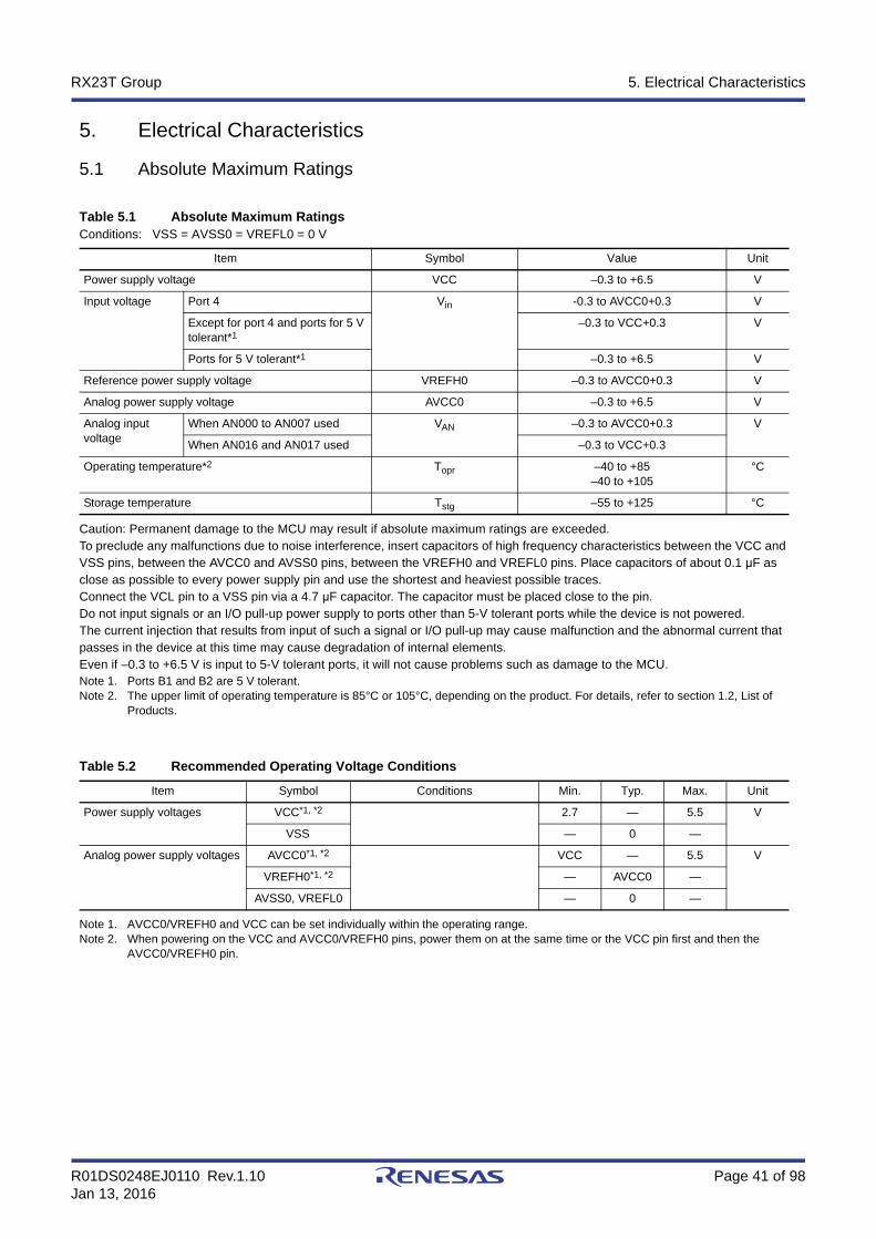
R01DS0248EJ0110 Rev.1.10 Page 41 of 98Jan 13, 2016
RX23T Group 5. Electrical Characteristics
5. Electrical Characteristics
5.1 Absolute Maximum Ratings
Caution: Permanent damage to the MCU may result if absolute maximum ratings are exceeded.To preclude any malfunctions due to noise interference, insert capacitors of high frequency characteristics between the VCC and VSS pins, between the AVCC0 and AVSS0 pins, between the VREFH0 and VREFL0 pins. Place capacitors of about 0.1 μF as close as possible to every power supply pin and use the shortest and heaviest possible traces.Connect the VCL pin to a VSS pin via a 4.7 μF capacitor. The capacitor must be placed close to the pin.Do not input signals or an I/O pull-up power supply to ports other than 5-V tolerant ports while the device is not powered.The current injection that results from input of such a signal or I/O pull-up may cause malfunction and the abnormal current that passes in the device at this time may cause degradation of internal elements.Even if –0.3 to +6.5 V is input to 5-V tolerant ports, it will not cause problems such as damage to the MCU.Note 1. Ports B1 and B2 are 5 V tolerant.Note 2. The upper limit of operating temperature is 85°C or 105°C, depending on the product. For details, refer to section 1.2, List of
Products.
Note 1. AVCC0/VREFH0 and VCC can be set individually within the operating range.Note 2. When powering on the VCC and AVCC0/VREFH0 pins, power them on at the same time or the VCC pin first and then the
AVCC0/VREFH0 pin.
Table 5.1 Absolute Maximum RatingsConditions: VSS = AVSS0 = VREFL0 = 0 V
Item Symbol Value Unit
Power supply voltage VCC –0.3 to +6.5 V
Input voltage Port 4 Vin -0.3 to AVCC0+0.3 V
Except for port 4 and ports for 5 V tolerant*1
–0.3 to VCC+0.3 V
Ports for 5 V tolerant*1 –0.3 to +6.5 V
Reference power supply voltage VREFH0 –0.3 to AVCC0+0.3 V
Analog power supply voltage AVCC0 –0.3 to +6.5 V
Analog input voltage
When AN000 to AN007 used VAN –0.3 to AVCC0+0.3 V
When AN016 and AN017 used –0.3 to VCC+0.3
Operating temperature*2 Topr –40 to +85–40 to +105
°C
Storage temperature Tstg –55 to +125 °C
Table 5.2 Recommended Operating Voltage Conditions
Item Symbol Conditions Min. Typ. Max. Unit
Power supply voltages VCC*1, *2 2.7 — 5.5 V
VSS — 0 —
Analog power supply voltages AVCC0*1, *2 VCC — 5.5 V
VREFH0*1, *2 — AVCC0 —
AVSS0, VREFL0 — 0 —

R01DS0248EJ0110 Rev.1.10 Page 42 of 98Jan 13, 2016
RX23T Group 5. Electrical Characteristics
5.2 DC Characteristics
Table 5.3 DC Characteristics (1)Conditions: VCC = 2.7 V to 5.5 V, AVCC0 = VREFH0 = VCC to 5.5 V, VSS = AVSS0 = VREFL0 = 0 V, Ta = –40 to +105°C
Item Symbol Min. Typ. Max. UnitTest
Conditions
Schmitt trigger input voltage
RIIC input pin(except for SMBus, 5 V tolerant)
VIH VCC × 0.7 — 5.8 V
Ports B1 and B2(5 V tolerant)
VCC × 0.8 — 5.8
Ports 00 to 02, 10, 11Ports 22 to 24Ports 30 to 33, 36, 37Ports 70 to 76Ports 91 to 94Ports A2 to A5Ports B0, B3 to B7Ports D3 to D7Port E2Port RES#
VCC × 0.8 — VCC + 0.3
Ports 40 to 47 AVCC0 × 0.8 — AVCC0 + 0.3
RIIC input pin (except for SMBus) VIL –0.3 — VCC × 0.3
Ports 40 to 47 –0.3 — AVCC0 × 0.2
Other than RIIC input pin or ports 40 to 47
–0.3 — VCC × 0.2
RIIC input pin (except for SMBus) ∆VT VCC × 0.05 — —
Ports 40 to 47 AVCC0 × 0.1 — —
Other than RIIC input pin or ports 40 to 47
VCC × 0.1 — —
Input level voltage (except for Schmitt trigger input pins)
MD VIH VCC × 0.9 — VCC + 0.3 V
EXTAL (external clock input) VCC × 0.8 — VCC + 0.3
RIIC input pin (SMBus) 2.1 — VCC + 0.3
MD VIL –0.3 — VCC × 0.1
EXTAL (external clock input) –0.3 — VCC × 0.2
RIIC input pin (SMBus) –0.3 — 0.8
Table 5.4 DC Characteristics (2)Conditions: VCC = 2.7 V to 5.5 V, AVCC0 = VREFH0 = VCC to 5.5 V, VSS = AVSS0 = VREFL0 = 0 V, Ta = –40 to +105°C
Item Symbol Min. Typ. Max. Unit Test Conditions
Input leakage current RES#, MD, port E2 Iin — — 1.0 μA Vin = 0 V, VCC
Three-state leakage current (off-state)
Port 4 ITSI — — 1.0 μA Vin = 0 V, AVCC0
Ports except for 5-V tolerant ports and port 4
— — 0.2 Vin = 0 V, VCC
Ports for 5 V tolerant — — 1.0 Vin = 0 V, 5.8 V
Input capacitance All input pins Cin — 4 15 pF Vin = 0 mV, f = 1 MHz, Ta = 25°C
Input pull-up resistor All ports(except for port E2)
RU 10 20 50 kΩ Vin = 0 V

R01DS0248EJ0110 Rev.1.10 Page 43 of 98Jan 13, 2016
RX23T Group 5. Electrical Characteristics
Table 5.5 DC Characteristics (3)Conditions: VCC = 2.7 V to 5.5 V, AVCC0 = VREFH0 = VCC to 5.5 V, VSS = AVSS0 = VREFL0 = 0 V, Ta = –40 to +105°C
Item Symbol Typ. Max. UnitTest
Conditions
Supply current*1
High-speed operating mode
Normal operating mode
No peripheral operation*2
ICLK = 40 MHz ICC 4.6 — mA
ICLK = 32 MHz 3.9 —
ICLK = 16 MHz 2.8 —
ICLK = 8 MHz 2.2 —
All peripheral operation: Normal
ICLK = 40 MHz*3 15.0 —
ICLK = 32 MHz*4 12.4 —
ICLK = 16 MHz*4 7.2 —
ICLK = 8 MHz*4 4.6 —
All peripheral operation: Max.
ICLK = 40 MHz*3 — 33.0
ICLK = 32 MHz*4 — 24.5
Sleep mode No peripheral operation*2
ICLK = 40 MHz 2.7 —
ICLK = 32 MHz 2.3 —
ICLK = 16 MHz 1.9 —
ICLK = 8 MHz 1.6 —
All peripheral operation: Normal
ICLK = 40 MHz*3 6.8 —
ICLK = 32 MHz*4 5.7 —
ICLK = 16 MHz*4 3.6 —
ICLK = 8 MHz*4 2.5 —
Deep sleep mode
No peripheral operation*2
ICLK = 40 MHz 1.7 —
ICLK = 32 MHz 1.5 —
ICLK = 16 MHz 1.3 —
ICLK = 8 MHz 1.3 —
All peripheral operation: Normal
ICLK = 40 MHz*3 5.3 —
ICLK = 32 MHz*4 4.4 —
ICLK = 16 MHz*4 2.8 —
ICLK = 8 MHz*4 2.0 —
Middle-speed operating modes
Normal operating mode
No peripheral operation*6
ICLK = 12 MHz ICC 2.6 — mA
ICLK = 8 MHz 1.9 —
ICLK = 1 MHz 1.3 —
All peripheral operation: Normal*7
ICLK = 12 MHz 5.5 —
ICLK = 8 MHz 4.2 —
ICLK = 1 MHz 1.6 —
All peripheral operation: Max.*7
ICLK = 12 MHz — 11.0

R01DS0248EJ0110 Rev.1.10 Page 44 of 98Jan 13, 2016
RX23T Group 5. Electrical Characteristics
Note 1. Supply current values do not include output charge/discharge current from all pins. The values apply when internal pull-up MOSs are in the off state.
Note 2. Supply of the clock signal to peripheral modules is stopped in this state. The clock source is PLL. FCLK and PCLK are division by 64.
Note 3. The clock signal to peripheral modules is supplied in this state. The clock source is PLL. FCLK is division by 2. The frequency of PCLK is same as ICLK.
Note 4. The clock signal to peripheral modules is supplied in this state. The clock source is PLL. The frequencies of FCLK and PCLK are same as ICLK.
Note 5. Values when VCC = 5 V.Note 6. Supply of the clock signal to peripheral modules is stopped in this state. The clock source is PLL. FCLK and PCLK are division
by 64. Note 7. Supply of the clock signal to peripheral modules is stopped in this state. The clock source is PLL. The frequencies of FCLK and
PCLK are same as ICLK.
Note 1. Supply current values are with all output pins unloaded and all input pull-up MOSs in the off state.Note 2. The IWDT and LVD are stopped.Note 3. VCC = 5 V.
Supply current*1
Middle-speed operating modes
Sleep mode No peripheral operation*6
ICLK = 12 MHz ICC 2.0 — mA
ICLK = 8 MHz 1.4 —
ICLK = 1 MHz 1.2 —
All peripheral operation: Normal*7
ICLK = 12 MHz 2.8 —
ICLK = 8 MHz 2.3 —
ICLK = 1 MHz 1.3 —
Deep sleep mode
No peripheral operation*6
ICLK = 12 MHz 1.5 —
ICLK = 8 MHz 1.2 —
ICLK = 1 MHz 1.1 —
All peripheral operation: Normal*7
ICLK = 12 MHz 2.8 —
ICLK = 8 MHz 2.3 —
ICLK = 1 MHz 1.1 —
Table 5.6 DC Characteristics (4)Conditions: VCC = 2.7 V to 5.5 V, AVCC0 = VREFH0 = VCC to 5.5 V, VSS = AVSS0 = VREFL0 = 0 V, Ta = –40 to +105°C
Item Symbol Typ.*3 Max. Unit Test Conditions
Supply current*1
Software standby mode*2
Ta = 25°C ICC 0.45 0.91 μA
Ta = 55°C 0.66 2.23
Ta = 85°C 1.50 9.14
Ta = 105°C 3.42 23.94
Item Symbol Typ. Max. UnitTest
Conditions
R01DS0248EJ0110 Rev.1.10 Page 45 of 98Jan 13, 2016
RX23T Group 5. Electrical Characteristics
Figure 5.1 Voltage Dependency in Software Standby Mode (Reference Data)
Figure 5.2 Temperature Dependency in Software Standby Mode (Reference Data)
100
10
1
0
2.0 2.5 3.0 3.5 4.0 4.5 6.05.0 5.5
Ta = 25°C*2
Ta = 25°C*1
Ta = 55°C*2
Ta = 55°C*1
Ta = 85°C*2
Ta = 85°C*1
Ta = 105°C*2
Ta = 105°C*1
ICC
(A
)
Ta = 105°C*2
Ta = 85°C*2
Ta = 105°C*1
Ta = 85°C*1
Ta = 55°C*2
Ta = 55°C*1
Ta = 25°C*2
Ta = 25°C*1
VCC (V)
Note 1. Average value of the tested middle samples during product evaluation.Note 2. Average value of the tested upper-limit samples during product evaluation.
Average value of the tested middle samples during product evaluation.Average value of the tested upper-limit samples during product evaluation.
ICC
(A
)
Ta (°C)
10
1
-40
0.1
100
0 40 80 120-20 20 60 100
R01DS0248EJ0110 Rev.1.10 Page 46 of 98Jan 13, 2016
RX23T Group 5. Electrical Characteristics
Note: Please contact a Renesas Electronics sales office for information on the derating of the G-version product. Derating is the systematic reduction of load for the sake of improved reliability.
Note 1. Total power dissipated by the entire chip (including output currents)
Note 1. The value of the D/A converter is the value of the power supply current including the reference current.Note 2. When VCC = AVCC0 = 5 V.Note 3. Current consumed only by the comparator C module.
Note 1. When OFS1.LVDAS = 0.Note 2. Turn on the power supply voltage according to the normal startup rising gradient because the register settings set by OFS1 are
not read in boot mode.
Table 5.7 DC Characteristics (5)Conditions: VCC = 2.7 V to 5.5 V, AVCC0 = VREFH0 = VCC to 5.5 V, VSS = AVSS0 = VREFL0 = 0 V, Ta = –40 to +105°C
Item Symbol Typ. Max. Unit Test Conditions
Permissible total consumption power*1 Pd — 300 mW D-version product
Permissible total consumption power*1 Pd — 125 mW G-version product
Table 5.8 DC Characteristics (6)Conditions: VCC = 2.7 V to 5.5 V, AVCC0 = VREFH0 = VCC to 5.5 V, VSS = AVSS0 = VREFL0 = 0 V, Ta = –40 to +105°C
Item Symbol Min. Typ.*2 Max. Unit Test Conditions
Analog power supply current
During A/D conversion (Sample-and-hold circuits in use)
IAVCC — 3.1 5.2 mA
During A/D conversion (Sample-and-hold circuits not in use)
— 0.9 1.8
During D/A conversion*1 — 0.4 0.9
Waiting for A/D and D/A conversion (all units) — — 0.4 μA
Reference power supply current
During A/D conversion IREFH0 — 80 130 μA
Waiting for A/D conversion (all units) — — 60 nA
Comparator C operating current*3
Comparator enabled (per channel) ICMP — 40 60 μA
Table 5.9 DC Characteristics (7)Conditions: VCC = 2.7 V to 5.5 V, AVCC0 = VREFH0 = VCC to 5.5 V, VSS = AVSS0 = VREFL0 = 0 V, Ta = –40 to +105°C
Item Symbol Min. Typ. Max. Unit Test Conditions
Power-on VCC rising gradient
At normal startup SrVCC 0.02 — 20 ms/V
Voltage monitoring 0 reset enabled at startup*1, *2
0.02 — —

R01DS0248EJ0110 Rev.1.10 Page 47 of 98Jan 13, 2016
RX23T Group 5. Electrical Characteristics
Figure 5.3 Ripple Waveform
Note: The recommended capacitance is 4.7 μF. Variations in connected capacitors should be within the above range.
Note: Do not exceed the permissible total supply current.
Table 5.10 DC Characteristics (8)Conditions: VCC = 2.7 V to 5.5 V, AVCC0 = VREFH0 = VCC to 5.5 V, VSS = AVSS0 = VREFL0 = 0 V, Ta = –40 to +105°C
The ripple voltage must meet the allowable ripple frequency fr (VCC) within the range between the VCC upper limit (5.5 V) and lower limit (2.7 V). When VCC change exceeds VCC ±10%, the allowable voltage change rising/falling gradient dt/dVCC must be met.
Item Symbol Min. Typ. Max. Unit Test Conditions
Allowable ripple frequency fr (VCC) — — 10 kHz Figure 5.3Vr (VCC) ≤ VCC × 0.2
— — 1 MHz Figure 5.3Vr (VCC) ≤ VCC × 0.08
— — 10 MHz Figure 5.3Vr (VCC) ≤ VCC × 0.06
Allowable voltage change rising/falling gradient
dt/dVCC 1.0 — — ms/V When VCC change exceeds VCC ±10%
Table 5.11 DC Characteristics (9)Conditions: VCC = 2.7 V to 5.5 V, AVCC0 = VREFH0 = VCC to 5.5 V, VSS = AVSS0 = VREFL0 = 0 V, Ta = –40 to +105°C
Item Symbol Min. Typ. Max. Unit Test Conditions
Permissible error of VCL pin external capacitance
CVCL 3.3 4.7 6.1 μF
Table 5.12 Permissible Output CurrentsConditions: VCC = 2.7 V to 5.5 V, AVCC0 = VREFH0 = VCC to 5.5 V, VSS = AVSS0 = VREFL0 = 0 V, Ta = –40 to +105°C
Item Symbol Max. Unit
Permissible output low current Large current ports (Ports 71 to 76, port B5, port D3) IOL 10.0 mA
RIIC pins 6.0
Ports other than above Normal output mode 4.0
High-drive output mode 8.0
Permissible output low current Total of large current ports IOL 50
Total of all output pins 110
Permissible output high current Large current ports (Ports 71 to 76, port B5, port D3) IOH –5.0
Ports other than above Normal output mode –4.0
High-drive output mode –8.0
Permissible output high current Total of large current ports IOH –25
Total of all output pins –35
Vr (VCC)VCC
1 / fr (VCC)

R01DS0248EJ0110 Rev.1.10 Page 48 of 98Jan 13, 2016
RX23T Group 5. Electrical Characteristics
5.2.1 Normal I/O Pin Output Characteristics (1)
Figure 5.4 to Figure 5.7 show the characteristics when normal output is selected by the drive capacity control register.
Figure 5.4 VOH/VOL and IOH/IOL Voltage Characteristics at Ta = 25°C When Normal Output is Selected
(Reference Data)
Table 5.13 Output Values of VoltageConditions: VCC = 2.7 V to 5.5 V, AVCC0 = VREFH0 = VCC to 5.5 V, VSS = AVSS0 = VREFL0 = 0 V, Ta = –40 to +105°C
Item Symbol Min. Max. Unit Test Conditions
Output low Large current ports (Ports 71 to 76, port B5, port D3)
VOL — 0.8 V IOL = 10.0mA
RIIC pins Standard mode — 0.4 IOL = 3.0mA
Fast mode — 0.6 IOL = 6.0mA
Ports other than above
Normal output mode — 0.8 IOL = 1.0mA
High-drive output mode — 0.8 IOL = 2.0mA
Output high Large current ports (Ports 71 to 76, port B5, port D3)
VOH VCC – 0.8 — V IOH = –5.0mA
Ports 40 to 47 AVCC0 – 0.8 — IOH = –2.0mA
Ports other than above
Normal output mode VCC – 0.8 — IOH = –2.0mA
High-drive output mode VCC – 0.8 — IOH = –4.0mA
IOH/IOL vs VOH/VOL
60
40
20
0
-20
-40
-60
0.0 1.0 2.0 3.0 4.0 5.0 6.0
I OH/I
OL[m
A]
VCC = 5.5 V
VCC = 5.0 V
VCC = 2.7 V
VCC = 2.7 V
VCC = 5.0 V
VCC = 5.5 V
VOH/VOL[V]
R01DS0248EJ0110 Rev.1.10 Page 49 of 98Jan 13, 2016
RX23T Group 5. Electrical Characteristics
Figure 5.5 VOH/VOL and IOH/IOL Temperature Characteristics at VCC = 2.7 V when Normal Output is Selected
(Reference Data)
Figure 5.6 VOH/VOL and IOH/IOL Temperature Characteristics at VCC = 5.0 V when Normal Output is Selected
(Reference Data)
IOH/IOL vs VOH/VOL
20
15
5
0
-5
-15
-20
0.0 0.5 1.0 1.5 2.0 2.5 3.0
I OH/I
OL[m
A]
Ta = 25°C
Ta = 105°C
VOH/VOL[V]
10
-10Ta = 25°C
Ta = -40°C
Ta = 105°C
Ta = -40°C
IOH/IOL vs VOH/VOL
60
40
20
0
-20
-40
-60
0.0 1.0 2.0 3.0 4.0 5.0 6.0
I OH/I
OL[
mA
]
VOH/VOL[V]
Ta = 25°C
Ta = 105°C
Ta = 25°CTa = -40°C
Ta = 105°C
Ta = -40°C

R01DS0248EJ0110 Rev.1.10 Page 50 of 98Jan 13, 2016
RX23T Group 5. Electrical Characteristics
Figure 5.7 VOH/VOL and IOH/IOL Temperature Characteristics at VCC = 5.5 V when Normal Output is Selected
(Reference Data)
IOH/IOL vs VOH/VOL
60
40
20
0
-20
-40
-60
0.0 1.0 2.0 3.0 4.0 5.0 6.0
I OH/I
OL[m
A]
VOH/VOL[V]
Ta = 25°C
Ta = 105°CTa = 25°CTa = -40°C
Ta = 105°C
Ta = -40°C

R01DS0248EJ0110 Rev.1.10 Page 51 of 98Jan 13, 2016
RX23T Group 5. Electrical Characteristics
5.2.2 Standard I/O Pin Output Characteristics (2)
Figure 5.8 to Figure 5.11 show the characteristics when high-drive output is selected by the drive capacity control
register.
Figure 5.8 VOH/VOL and IOH/IOL Voltage Characteristics at Ta = 25°C When Normal Output is Selected
(Reference Data)
Figure 5.9 VOH/VOL and IOH/IOL Temperature Characteristics at VCC = 2.7 V when Normal Output is Selected
(Reference Data)
IOH/IOL vs VOH/VOL
0.0 1.0 2.0 3.0 4.0 5.0 6.0
VOH/VOL[V]
150
100
50
0
-50
-100
-150
I OH/I
OL[
mA
]
VCC = 5.5 V
VCC = 5.0 V
VCC = 2.7 V
VCC = 2.7 V
VCC = 5.0 V
VCC = 5.5 V
IOH/IOL vs VOH/VOL
40
30
10
0
-10
-30
-40
0.0 0.5 1.0 1.5 2.0 2.5 3.0
I OH/I
OL[m
A]
Ta = 25°C
Ta = 105°C
VOH/VOL[V]
20
-20Ta = 25°C
Ta = -40°C
Ta = 105°C
Ta = -40°C

R01DS0248EJ0110 Rev.1.10 Page 52 of 98Jan 13, 2016
RX23T Group 5. Electrical Characteristics
Figure 5.10 VOH/VOL and IOH/IOL Temperature Characteristics at VCC = 5.0 V when Normal Output is Selected
(Reference Data)
Figure 5.11 VOH/VOL and IOH/IOL Temperature Characteristics at VCC = 5.5 V when Normal Output is Selected
(Reference Data)
IOH/IOL vs VOH/VOL
150
100
50
0
-50
-100
-150
0.0 1.0 2.0 3.0 4.0 5.0 6.0
I OH/I
OL[m
A]
VOH/VOL[V]
Ta = 25°C
Ta = 105°C
Ta = 25°C
Ta = -40°C
Ta = 105°C
Ta = -40°C
IOH/IOL vs VOH/VOL
150
100
50
0
-50
-100
-150
0.0 1.0 2.0 3.0 4.0 5.0 6.0
I OH/I
OL[
mA
]
VOH/VOL[V]
Ta = 25°C
Ta = 105°CTa = 25°CTa = -40°C
Ta = 105°C
Ta = -40°C
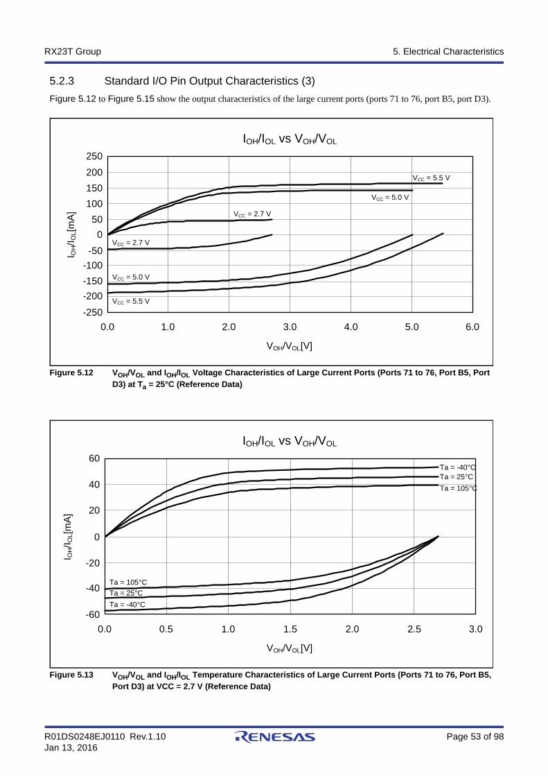
R01DS0248EJ0110 Rev.1.10 Page 53 of 98Jan 13, 2016
RX23T Group 5. Electrical Characteristics
5.2.3 Standard I/O Pin Output Characteristics (3)
Figure 5.12 to Figure 5.15 show the output characteristics of the large current ports (ports 71 to 76, port B5, port D3).
Figure 5.12 VOH/VOL and IOH/IOL Voltage Characteristics of Large Current Ports (Ports 71 to 76, Port B5, Port
D3) at Ta = 25°C (Reference Data)
Figure 5.13 VOH/VOL and IOH/IOL Temperature Characteristics of Large Current Ports (Ports 71 to 76, Port B5,
Port D3) at VCC = 2.7 V (Reference Data)
IOH/IOL vs VOH/VOL
250
150
100
0
-100
-150
-250
0.0 1.0 2.0 3.0 4.0 5.0 6.0
I OH/I
OL[m
A]
VCC = 5.5 V
VCC = 5.0 V
VCC = 2.7 V
VCC = 2.7 V
VCC = 5.0 V
VCC = 5.5 V
VOH/VOL[V]
200
50
-50
-200
IOH/IOL vs VOH/VOL
60
40
20
0
-20
-40
-60
0.0 0.5 1.0 1.5 2.0 2.5 3.0
I OH/I
OL[
mA
]
Ta = 25°C
Ta = 105°C
VOH/VOL[V]
Ta = 25°C
Ta = -40°C
Ta = 105°C
Ta = -40°C

R01DS0248EJ0110 Rev.1.10 Page 54 of 98Jan 13, 2016
RX23T Group 5. Electrical Characteristics
Figure 5.14 VOH/VOL and IOH/IOL Temperature Characteristics of Large Current Ports (Ports 71 to 76, Port B5,
Port D3) at VCC = 5.0 V (Reference Data)
Figure 5.15 VOH/VOL and IOH/IOL Temperature Characteristics of Large Current Ports (Ports 71 to 76, Port B5,
Port D3) at VCC = 5.5 V (Reference Data)
5.2.4 RIIC Pin Output Characteristics
Figure 5.16 to Figure 5.19 show the output characteristics of the RIIC pin.
IOH/IOL vs VOH/VOL
250
150
100
0
-100
-150
-250
0.0 1.0 2.0 3.0 4.0 5.0 6.0
I OH/I
OL[m
A]
VOH/VOL[V]
Ta = 25°C
Ta = 105°C
Ta = 25°C
Ta = -40°C
Ta = 105°C
Ta = -40°C200
50
-50
-200
IOH/IOL vs VOH/VOL
250
150
100
0
-100
-150
-250
0.0 1.0 2.0 3.0 4.0 5.0 6.0
I OH/I
OL[m
A]
VOH/VOL[V]
Ta = 25°C
Ta = 105°C
Ta = 25°C
Ta = -40°C
Ta = 105°C
Ta = -40°C200
50
-50
-200
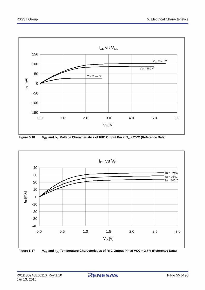
R01DS0248EJ0110 Rev.1.10 Page 55 of 98Jan 13, 2016
RX23T Group 5. Electrical Characteristics
Figure 5.16 VOL and IOL Voltage Characteristics of RIIC Output Pin at Ta = 25°C (Reference Data)
Figure 5.17 VOL and IOL Temperature Characteristics of RIIC Output Pin at VCC = 2.7 V (Reference Data)
IOL vs VOL
150
100
50
0
-50
-100
-150
0.0 1.0 2.0 3.0 4.0 5.0 6.0
I OL[
mA
]
VCC = 5.5 V
VCC = 5.0 V
VCC = 2.7 V
VOL[V]
IOL vs VOL
40
30
10
0
-10
-30
-40
0.0 0.5 1.0 1.5 2.0 2.5 3.0
I OL[m
A]
Ta = 25°C
VOL[V]
20
-20
Ta = 105°C
Ta = -40°C
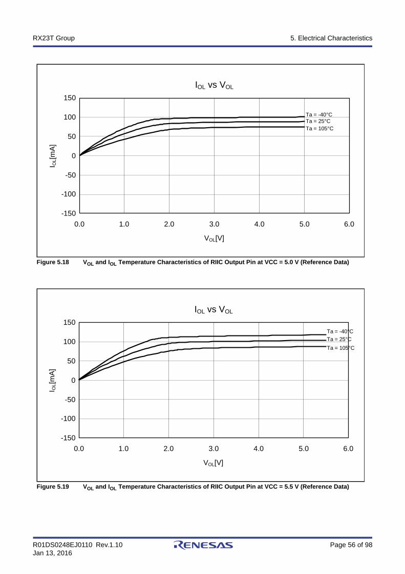
R01DS0248EJ0110 Rev.1.10 Page 56 of 98Jan 13, 2016
RX23T Group 5. Electrical Characteristics
Figure 5.18 VOL and IOL Temperature Characteristics of RIIC Output Pin at VCC = 5.0 V (Reference Data)
Figure 5.19 VOL and IOL Temperature Characteristics of RIIC Output Pin at VCC = 5.5 V (Reference Data)
IOL vs VOL
150
100
50
0
-50
-100
-150
0.0 1.0 2.0 3.0 4.0 5.0 6.0
I OL[
mA
]
VOL[V]
Ta = 25°CTa = 105°C
Ta = -40°C
IOL vs VOL
150
100
50
0
-50
-100
-150
0.0 1.0 2.0 3.0 4.0 5.0 6.0
I OL[
mA
]
VOL[V]
Ta = 25°C
Ta = 105°C
Ta = -40°C
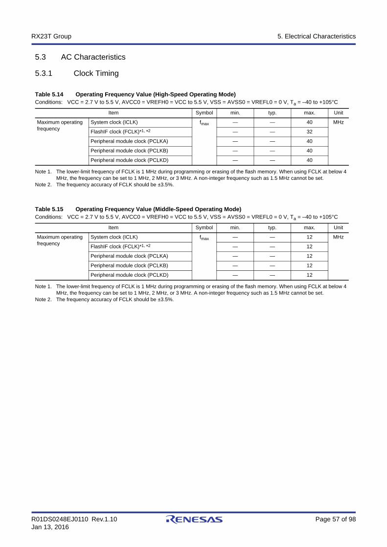
R01DS0248EJ0110 Rev.1.10 Page 57 of 98Jan 13, 2016
RX23T Group 5. Electrical Characteristics
5.3 AC Characteristics
5.3.1 Clock Timing
Note 1. The lower-limit frequency of FCLK is 1 MHz during programming or erasing of the flash memory. When using FCLK at below 4 MHz, the frequency can be set to 1 MHz, 2 MHz, or 3 MHz. A non-integer frequency such as 1.5 MHz cannot be set.
Note 2. The frequency accuracy of FCLK should be ±3.5%.
Note 1. The lower-limit frequency of FCLK is 1 MHz during programming or erasing of the flash memory. When using FCLK at below 4 MHz, the frequency can be set to 1 MHz, 2 MHz, or 3 MHz. A non-integer frequency such as 1.5 MHz cannot be set.
Note 2. The frequency accuracy of FCLK should be ±3.5%.
Table 5.14 Operating Frequency Value (High-Speed Operating Mode)Conditions: VCC = 2.7 V to 5.5 V, AVCC0 = VREFH0 = VCC to 5.5 V, VSS = AVSS0 = VREFL0 = 0 V, Ta = –40 to +105°C
Item Symbol min. typ. max. Unit
Maximum operating frequency
System clock (ICLK) fmax — — 40 MHz
FlashIF clock (FCLK)*1, *2 — — 32
Peripheral module clock (PCLKA) — — 40
Peripheral module clock (PCLKB) — — 40
Peripheral module clock (PCLKD) — — 40
Table 5.15 Operating Frequency Value (Middle-Speed Operating Mode)Conditions: VCC = 2.7 V to 5.5 V, AVCC0 = VREFH0 = VCC to 5.5 V, VSS = AVSS0 = VREFL0 = 0 V, Ta = –40 to +105°C
Item Symbol min. typ. max. Unit
Maximum operating frequency
System clock (ICLK) fmax — — 12 MHz
FlashIF clock (FCLK)*1, *2 — — 12
Peripheral module clock (PCLKA) — — 12
Peripheral module clock (PCLKB) — — 12
Peripheral module clock (PCLKD) — — 12
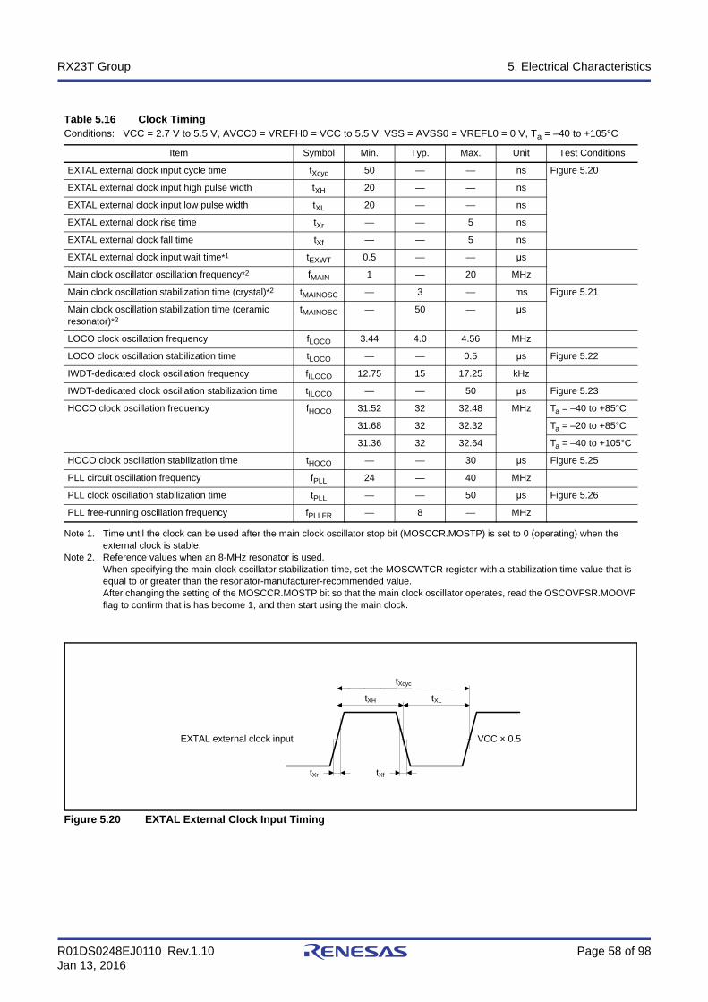
R01DS0248EJ0110 Rev.1.10 Page 58 of 98Jan 13, 2016
RX23T Group 5. Electrical Characteristics
Note 1. Time until the clock can be used after the main clock oscillator stop bit (MOSCCR.MOSTP) is set to 0 (operating) when the external clock is stable.
Note 2. Reference values when an 8-MHz resonator is used.When specifying the main clock oscillator stabilization time, set the MOSCWTCR register with a stabilization time value that is equal to or greater than the resonator-manufacturer-recommended value.After changing the setting of the MOSCCR.MOSTP bit so that the main clock oscillator operates, read the OSCOVFSR.MOOVF flag to confirm that is has become 1, and then start using the main clock.
Figure 5.20 EXTAL External Clock Input Timing
Table 5.16 Clock TimingConditions: VCC = 2.7 V to 5.5 V, AVCC0 = VREFH0 = VCC to 5.5 V, VSS = AVSS0 = VREFL0 = 0 V, Ta = –40 to +105°C
Item Symbol Min. Typ. Max. Unit Test Conditions
EXTAL external clock input cycle time tXcyc 50 — — ns Figure 5.20
EXTAL external clock input high pulse width tXH 20 — — ns
EXTAL external clock input low pulse width tXL 20 — — ns
EXTAL external clock rise time tXr — — 5 ns
EXTAL external clock fall time tXf — — 5 ns
EXTAL external clock input wait time*1 tEXWT 0.5 — — μs
Main clock oscillator oscillation frequency*2 fMAIN 1 — 20 MHz
Main clock oscillation stabilization time (crystal)*2 tMAINOSC — 3 — ms Figure 5.21
Main clock oscillation stabilization time (ceramic resonator)*2
tMAINOSC — 50 — μs
LOCO clock oscillation frequency fLOCO 3.44 4.0 4.56 MHz
LOCO clock oscillation stabilization time tLOCO — — 0.5 μs Figure 5.22
IWDT-dedicated clock oscillation frequency fILOCO 12.75 15 17.25 kHz
IWDT-dedicated clock oscillation stabilization time tILOCO — — 50 μs Figure 5.23
HOCO clock oscillation frequency fHOCO 31.52 32 32.48 MHz Ta = –40 to +85°C
31.68 32 32.32 Ta = –20 to +85°C
31.36 32 32.64 Ta = –40 to +105°C
HOCO clock oscillation stabilization time tHOCO — — 30 μs Figure 5.25
PLL circuit oscillation frequency fPLL 24 — 40 MHz
PLL clock oscillation stabilization time tPLL — — 50 μs Figure 5.26
PLL free-running oscillation frequency fPLLFR — 8 — MHz
tXH
tXcyc
EXTAL external clock input VCC × 0.5
tXL
tXr tXf

R01DS0248EJ0110 Rev.1.10 Page 59 of 98Jan 13, 2016
RX23T Group 5. Electrical Characteristics
Figure 5.21 Main Clock Oscillation Start Timing
Figure 5.22 LOCO Clock Oscillation Start Timing
Figure 5.23 IWDT-Dedicated Clock Oscillation Start Timing
Figure 5.24 HOCO Clock Oscillation Start Timing (After Reset is Canceled by Setting OFS1.HOCOEN Bit to 0)
Main clock oscillator output
MOSCCR.MOSTP
tMAINOSC
LOCO clock oscillator output
LOCOCR.LCSTP
tLOCO
IWDT-dedicated clock oscillator output
ILOCOCR.ILCSTP
tILOCO
RES#
Internal reset
HOCO clock
OFS1.HOCOEN
tRESWT
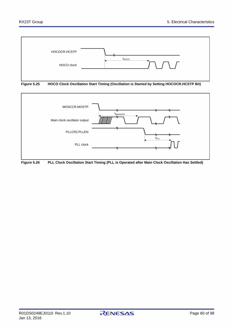
R01DS0248EJ0110 Rev.1.10 Page 60 of 98Jan 13, 2016
RX23T Group 5. Electrical Characteristics
Figure 5.25 HOCO Clock Oscillation Start Timing (Oscillation is Started by Setting HOCOCR.HCSTP Bit)
Figure 5.26 PLL Clock Oscillation Start Timing (PLL is Operated after Main Clock Oscillation Has Settled)
HOCO clock
HOCOCR.HCSTP
tHOCO
PLLCR2.PLLEN
PLL clock
MOSCCR.MOSTP
tMAINOSC
Main clock oscillator output
tPLL

R01DS0248EJ0110 Rev.1.10 Page 61 of 98Jan 13, 2016
RX23T Group 5. Electrical Characteristics
5.3.2 Reset Timing
Note 1. When IWDTCR.CKS[3:0] = 0000b.
Figure 5.27 Reset Input Timing at Power-On
Figure 5.28 Reset Input Timing (1)
Figure 5.29 Reset Input Timing (2)
Table 5.17 Reset TimingConditions: VCC = 2.7 V to 5.5 V, AVCC0 = VREFH0 = VCC to 5.5 V, VSS = AVSS0 = VREFL0 = 0 V, Ta = –40 to +105°C
Item Symbol Min. Typ. Max. Unit Test Conditions
RES# pulse width At power-on tRESWP 3 — — ms Figure 5.27
Other than above tRESW 30 — — μs Figure 5.28
Wait time after RES# cancellation (at power-on) tRESWT — 27.5 — ms Figure 5.27
Wait time after RES# cancellation(during powered-on state)
tRESWT — 114 — μs Figure 5.28
Independent watchdog timer reset period tRESWIW — 1 — IWDT clock cycle
Figure 5.29
Software reset period tRESWSW — 1 — ICLK cycle
Wait time after independent watchdog timer reset cancellation*1 tRESW2 — 300 — μs
Wait time after software reset cancellation tRESW2 — 168 — μs
VCC
RES#
tRESWP
Internal reset
tRESWT
RES#
Internal reset
tRESWT
tRESW
Independent watchdog timer resetSoftware reset
Internal reset
tRESWT2
tRESWIW, tRESWSW

R01DS0248EJ0110 Rev.1.10 Page 62 of 98Jan 13, 2016
RX23T Group 5. Electrical Characteristics
5.3.3 Timing of Recovery from Low Power Consumption Modes
Note 1. The recovery time varies depending on the state of each oscillator when the WAIT instruction is executed. The recovery time when multiple oscillators are operating varies depending on the operating state of the oscillators that are not selected as the system clock source. The above table applies when only the corresponding clock is operating.
Note 2. When the frequency of crystal is 20 MHz.When the main clock oscillator wait control register (MOSCWTCR) is set to 04h.
Note 3. When the frequency of the external clock is 20 MHz.When the main clock oscillator wait control register (MOSCWTCR) is set to 00h.
Note 4. When the frequency of PLL is 40 MHz. When the main clock oscillator wait control register (MOSCWTCR) is set to 00h.
Note 1. The recovery time varies depending on the state of each oscillator when the WAIT instruction is executed. The recovery time when multiple oscillators are operating varies depending on the operating state of the oscillators that are not selected as the system clock source. The above table applies when only the corresponding clock is operating.
Note 2. When the frequency of the crystal is 12 MHz.When the main clock oscillator wait control register (MOSCWTCR) is set to 04h.
Note 3. When the frequency of the external clock is 12 MHz.When the main clock oscillator wait control register (MOSCWTCR) is set to 00h.
Note 4. When the frequency of PLL is 12 MHz.When the main clock oscillator wait control register (MOSCWTCR) is set to 00h.
Table 5.18 Timing of Recovery from Low Power Consumption Modes (1)Conditions: VCC = 2.7 V to 5.5 V, AVCC0 = VREFH0 = VCC to 5.5 V, VSS = AVSS0 = VREFL0 = 0 V, Ta = –40 to +105°C
Item Symbol Min. Typ. Max. UnitTest
Conditions
Recovery time from software standby mode*1
High-speed mode
Crystal connected to main clock oscillator
Main clock oscillator operating*2
tSBYMC — 2 3 ms Figure 5.30
External clock input to main clock oscillator
Main clock oscillator operating*3
tSBYEX — 35 50 μs
Main clock oscillator and PLL circuit operating*4
tSBYPE — 70 95 μs
LOCO clock oscillator operating tSBYLO — 40 55 μs
Table 5.19 Timing of Recovery from Low Power Consumption Modes (2)Conditions: VCC = 2.7 V to 5.5 V, AVCC0 = VREFH0 = VCC to 5.5 V, VSS = AVSS0 = VREFL0 = 0 V, Ta = –40 to +105°C
Item Symbol Min. Typ. Max. UnitTest
Conditions
Recovery time from software standby mode*1
Middle-speed mode
Crystal connected to main clock oscillator
Main clock oscillator operating*2
tSBYMC — 2 3 ms Figure 5.30
External clock input to main clock oscillator
Main clock oscillator operating*3
tSBYEX — 3 4 μs
Main clock oscillator and PLL circuit operating*4
tSBYPE — 65 85 μs
LOCO clock oscillator operating tSBYLO — 5 7 μs
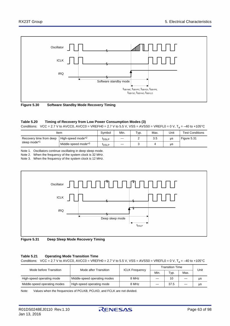
R01DS0248EJ0110 Rev.1.10 Page 63 of 98Jan 13, 2016
RX23T Group 5. Electrical Characteristics
Figure 5.30 Software Standby Mode Recovery Timing
Note 1. Oscillators continue oscillating in deep sleep mode.Note 2. When the frequency of the system clock is 32 MHz.Note 3. When the frequency of the system clock is 12 MHz.
Figure 5.31 Deep Sleep Mode Recovery Timing
Note: Values when the frequencies of PCLKB, PCLKD, and FCLK are not divided.
Table 5.20 Timing of Recovery from Low Power Consumption Modes (3)Conditions: VCC = 2.7 V to AVCC0, AVCC0 = VREFH0 = 2.7 V to 5.5 V, VSS = AVSS0 = VREFL0 = 0 V, Ta = –40 to +105°C
Item Symbol Min. Typ. Max. Unit Test Conditions
Recovery time from deep sleep mode*1
High-speed mode*2 tDSLP — 2 3.5 μs Figure 5.31
Middle-speed mode*3 tDSLP — 3 4 μs
Table 5.21 Operating Mode Transition TimeConditions: VCC = 2.7 V to AVCC0, AVCC0 = VREFH0 = 2.7 V to 5.5 V, VSS = AVSS0 = VREFL0 = 0 V, Ta = –40 to +105°C
Mode before Transition Mode after Transition ICLK FrequencyTransition Time
UnitMin. Typ. Max.
High-speed operating mode Middle-speed operating modes 8 MHz — 10 — μs
Middle-speed operating modes High-speed operating mode 8 MHz — 37.5 — μs
Oscillator
ICLK
IRQ
Software standby mode
tSBYMC, tSBYPC, tSBYEX, tSBYPE,
tSBYSC, tSBYHO, tSBYLO
Oscillator
ICLK
IRQ
Deep sleep mode
tDSLP

R01DS0248EJ0110 Rev.1.10 Page 64 of 98Jan 13, 2016
RX23T Group 5. Electrical Characteristics
5.3.4 Control Signal Timing
Note: 200 ns minimum in software standby mode.Note 1. tPcyc indicates the cycle of PCLKB.Note 2. tNMICK indicates the cycle of the NMI digital filter sampling clock.Note 3. tIRQCK indicates the cycle of the IRQi digital filter sampling clock (i = 0 to 5).
Figure 5.32 NMI Interrupt Input Timing
Figure 5.33 IRQ Interrupt Input Timing
Table 5.22 Control Signal TimingConditions: VCC = 2.7 V to 5.5 V, AVCC0 = VREFH0 = VCC to 5.5 V, VSS = AVSS0 = VREFL0 = 0 V, Ta = –40 to +105°C
Item Symbol Min. Typ. Max. Unit Test Conditions
NMI pulse width tNMIW 200 — — ns NMI digital filter disabled (NMIFLTE.NFLTEN = 0)
tPcyc × 2 ≤ 200 ns
tPcyc × 2*1 — — tPcyc × 2 > 200 ns
200 — — NMI digital filter enabled (NMIFLTE.NFLTEN = 1)
tNMICK × 3 ≤ 200 ns
tNMICK × 3.5*2 — — tNMICK × 3 > 200 ns
IRQ pulse width tIRQW 200 — — ns IRQ digital filter disabled (IRQFLTE0.FLTENi = 0)
tPcyc × 2 ≤ 200 ns
tPcyc × 2*1 — — tPcyc × 2 > 200 ns
200 — — IRQ digital filter enabled (IRQFLTE0.FLTENi = 1)
tIRQCK × 3 ≤ 200 ns
tIRQCK × 3.5*3 — — tIRQCK × 3 > 200 ns
NMI
tNMIW
IRQ
tIRQW

R01DS0248EJ0110 Rev.1.10 Page 65 of 98Jan 13, 2016
RX23T Group 5. Electrical Characteristics
5.3.5 Timing of On-Chip Peripheral Modules
Note 1. tPcyc: PCLK cycle, tPAcyc: PCLKA cycleNote 2. tcac: CAC count clock source cycle
Table 5.23 Timing of On-Chip Peripheral Modules (1)Conditions: VCC = 2.7 V to 5.5 V, AVCC0 = VREFH0 = VCC to 5.5 V, VSS = AVSS0 = VREFL0 = 0 V, Ta = –40 to +105°C
Item Symbol Min. Max.Unit
*1Test
Conditions
I/O ports Input data pulse width tPRW 1.5 — tPcyc Figure 5.34
MTU3 Input capture input pulse width Single-edge setting tTICW 3 — tPAcyc Figure 5.35
Both-edge setting 5 —
Timer clock pulse width Single-edge setting tTCKWH, tTCKWL
3 — tPAcyc Figure 5.36
Both-edge setting 5 —
Phase counting mode 5 —
POE3 POE# input pulse width tPOEW 1.5 — tPcyc Figure 5.37
TMR Timer clock pulse width Single-edge setting tTMCWH, tTMCWL
1.5 — tPcyc Figure 5.38
Both-edge setting 2.5 —
SCI Input clock cycle Asynchronous tScyc 4 — tPcyc Figure 5.39
Clock synchronous 6 —
Input clock pulse width tSCKW 0.4 0.6 tScyc
Input clock rise time tSCKr — 20 ns
Input clock fall time tSCKf — 20 ns
Output clock cycle Asynchronous tScyc 16 — tPcyc Figure 5.40
Clock synchronous 4 —
Output clock pulse width tSCKW 0.4 0.6 tScyc
Output clock rise time tSCKr — 20 ns
Output clock fall time tSCKf — 20 ns
Transmit data delay time (master)
Clock synchronous tTXD — 40 ns
Transmit data delay time (slave)
Clock synchronous
VCC = 4.0 V or above — 40 ns
VCC = 2.7 V or above — 65 ns
Receive data setup time (master)
Clock synchronous
VCC = 4.0 V or above tRXS 40 — ns
VCC = 2.7 V or above 65 — ns
Receive data setup time (slave)
Clock synchronous 40 — ns
Receive data hold time Clock synchronous tRXH 40 — ns
A/D converter Trigger input pulse width tTRGW 1.5 — tPcyc Figure 5.41
CAC CACREF input pulse width tPcyc ≤ tcac*2 tCACREF 4.5 tcac + 3 tPcyc — ns
tPcyc > tcac*2 5 tcac + 6.5 tPcyc

R01DS0248EJ0110 Rev.1.10 Page 66 of 98Jan 13, 2016
RX23T Group 5. Electrical Characteristics
Note 1. tPcyc: PCLK cycleNote 2. N: An integer from 1 to 8 that can be set by the RSPI clock delay register (SPCKD)Note 3. N: An integer from 1 to 8 that can be set by the RSPI slave select negation delay register (SSLND)
Table 5.24 Timing of On-Chip Peripheral Modules (2)Conditions: VCC = 2.7 V to 5.5 V, AVCC0 = VREFH0 = VCC to 5.5 V, VSS = AVSS0 = VREFL0 = 0 V, Ta = –40 to +105°C,
C = 30pF
Item Symbol Min. Max. UnitTest
Conditions
RSPI RSPCK clock cycle
Master tSPcyc 2 4096 tPcyc*1 Figure 5.42
Slave 8 4096
RSPCK clock high pulse width
Master VCC = 4.0 V or above tSPCKWH (tSPcyc – tSPCKr – tSPCKf)/2 – 5
— ns
VCC = 2.7 V or above (tSPcyc – tSPCKr – tSPCKf)/2 – 8
—
Slave (tSPcyc – tSPCKr – tSPCKf)/2
—
RSPCK clock low pulse width
Master VCC = 4.0 V or above tSPCKWL (tSPcyc – tSPCKr – tSPCKf)/2 – 5
— ns
VCC = 2.7 V or above (tSPcyc – tSPCKr– tSPCKf)/2 – 8
—
Slave (tSPcyc – tSPCKr – tSPCKf)/2
—
RSPCK clock rise/fall time
Output VCC = 4.0 V or above tSPCKr, tSPCKf
— 6 ns
VCC = 2.7 V or above — 10
Input — 0.1 μs/V
Data input setup time
Master VCC = 4.0 V or above tSU 10 — ns Figure 5.43 to Figure 5.46
VCC = 2.7 V or above 26 —
Slave 25 – tPcyc —
Data input hold time
Master RSPCK set to a division ratio other than PCLKB divided by 2
tH tPcyc — ns
RSPCK set to PCLKB divided by 2
tHF 0 —
Slave tH 20 + 2 × tPcyc —
SSL setup time Master tLEAD –30 + N*2 × tSPcyc — ns
Slave 2 — tPcyc
SSL hold time Master tLAG –30 + N*3 × tSPcyc — ns
Slave 2 — tPcyc
Data output delay time
Master VCC = 4.0 V or above tOD — 10 ns
VCC = 2.7 V or above — 14
Slave — 3 × tPcyc + 65
Data output hold time
Master 2.7 V or above tOH 0 — ns
Slave 0 —
Successive transmission delay time
Master tTD tSPcyc + 2 × tPcyc 8 × tSPcyc + 2 × tPcyc
ns
Slave 4 × tPcyc —
MOSI and MISO rise/fall time
Output tDr, tDf — 10 ns
Input — 1 μs
SSL rise/fall time
Output tSSLr, tSSLf
— 10 ns
Input — 1 μs
Slave access time tSA — 6 tPcyc Figure 5.45, Figure 5.46Slave output release time tREL — 5 tPcyc

R01DS0248EJ0110 Rev.1.10 Page 67 of 98Jan 13, 2016
RX23T Group 5. Electrical Characteristics
Note 1. tPcyc: PCLK cycle
Table 5.25 Timing of On-Chip Peripheral Modules (3)Conditions: VCC = 2.7 V to 5.5 V, AVCC0 = VREFH0 = VCC to 5.5 V, VSS = AVSS0 = VREFL0 = 0 V, Ta = –40 to +105°C,
C = 30pF
Item Symbol Min. Max. Unit*1 Test Conditions
Simple SPI
SCK clock cycle output (master) tSPcyc 4 65536 tPcyc Figure 5.42
SCK clock cycle input (slave) 6 65536 tPcyc
SCK clock high pulse width tSPCKWH 0.4 0.6 tSPcyc
SCK clock low pulse width tSPCKWL 0.4 0.6 tSPcyc
SCK clock rise/fall time tSPCKr, tSPCKf — 20 ns
Data input setup time (master) VCC = 4.0 V or above
tSU 40 — ns Figure 5.43, Figure 5.44
VCC = 2.7 V or above
65 —
Data input setup time (slave) 40 —
Data input hold time tH 40 — ns
SS input setup time tLEAD 3 — tSPcyc
SS input hold time tLAG 3 — tSPcyc
Data output delay time (master) tOD — 40 ns
Data output delay time (slave) VCC = 4.0 V or above
— 40
VCC = 2.7 V or above
— 65
Data output hold time (master) Master tOH –10 — ns
Slave –10 —
Data rise/fall time tDr, tDf — 20 ns
SS input rise/fall time tSSLr, tSSLf — 20 ns
Slave access time tSA — 6 tPcyc Figure 5.45, Figure 5.46
Slave output release time tREL — 6 tPcyc
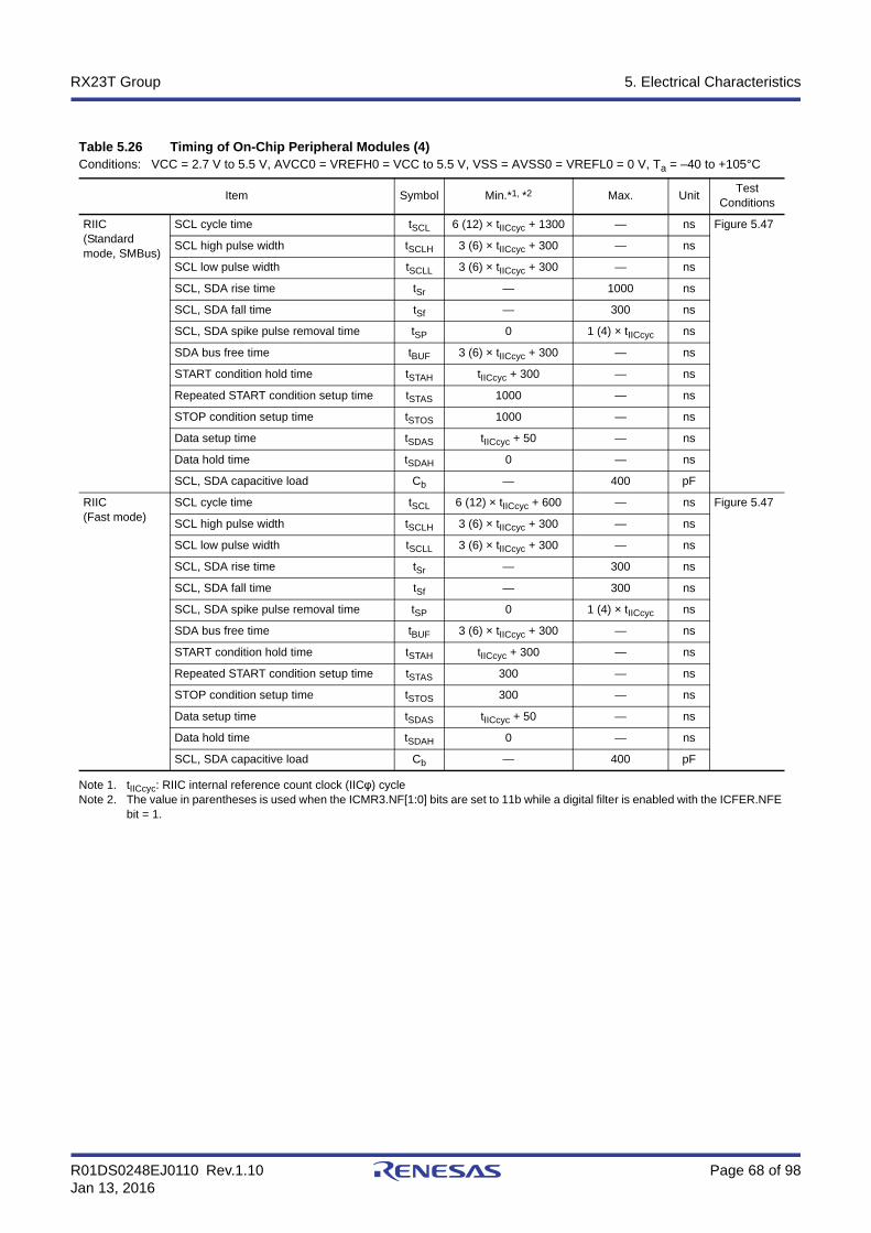
R01DS0248EJ0110 Rev.1.10 Page 68 of 98Jan 13, 2016
RX23T Group 5. Electrical Characteristics
Note 1. tIICcyc: RIIC internal reference count clock (IICφ) cycleNote 2. The value in parentheses is used when the ICMR3.NF[1:0] bits are set to 11b while a digital filter is enabled with the ICFER.NFE
bit = 1.
Table 5.26 Timing of On-Chip Peripheral Modules (4)Conditions: VCC = 2.7 V to 5.5 V, AVCC0 = VREFH0 = VCC to 5.5 V, VSS = AVSS0 = VREFL0 = 0 V, Ta = –40 to +105°C
Item Symbol Min.*1, *2 Max. UnitTest
Conditions
RIIC(Standard mode, SMBus)
SCL cycle time tSCL 6 (12) × tIICcyc + 1300 — ns Figure 5.47
SCL high pulse width tSCLH 3 (6) × tIICcyc + 300 — ns
SCL low pulse width tSCLL 3 (6) × tIICcyc + 300 — ns
SCL, SDA rise time tSr — 1000 ns
SCL, SDA fall time tSf — 300 ns
SCL, SDA spike pulse removal time tSP 0 1 (4) × tIICcyc ns
SDA bus free time tBUF 3 (6) × tIICcyc + 300 — ns
START condition hold time tSTAH tIICcyc + 300 — ns
Repeated START condition setup time tSTAS 1000 — ns
STOP condition setup time tSTOS 1000 — ns
Data setup time tSDAS tIICcyc + 50 — ns
Data hold time tSDAH 0 — ns
SCL, SDA capacitive load Cb — 400 pF
RIIC(Fast mode)
SCL cycle time tSCL 6 (12) × tIICcyc + 600 — ns Figure 5.47
SCL high pulse width tSCLH 3 (6) × tIICcyc + 300 — ns
SCL low pulse width tSCLL 3 (6) × tIICcyc + 300 — ns
SCL, SDA rise time tSr — 300 ns
SCL, SDA fall time tSf — 300 ns
SCL, SDA spike pulse removal time tSP 0 1 (4) × tIICcyc ns
SDA bus free time tBUF 3 (6) × tIICcyc + 300 — ns
START condition hold time tSTAH tIICcyc + 300 — ns
Repeated START condition setup time tSTAS 300 — ns
STOP condition setup time tSTOS 300 — ns
Data setup time tSDAS tIICcyc + 50 — ns
Data hold time tSDAH 0 — ns
SCL, SDA capacitive load Cb — 400 pF

R01DS0248EJ0110 Rev.1.10 Page 69 of 98Jan 13, 2016
RX23T Group 5. Electrical Characteristics
Note 1. tPcyc: PCLK cycleNote 2. Cb is the total capacitance of the bus lines.
Figure 5.34 I/O Port Input Timing
Figure 5.35 MTU3 Input/Output Timing
Table 5.27 Timing of On-Chip Peripheral Modules (5)Conditions: VCC = 2.7 V to 5.5 V, AVCC0 = VREFH0 = VCC to 5.5 V, VSS = AVSS0 = VREFL0 = 0 V, Ta = –40 to +105°C
Item Symbol Min.*2 Max. UnitTest
Conditions
Simple I2C(Standard mode)
SDA rise time tSr — 1000 ns Figure 5.47
SDA fall time tSf — 300 ns
SDA spike pulse removal time tSP 0 4 × tpcyc*1 ns
Data setup time tSDAS 250 — ns
Data hold time tSDAH 0 — ns
SCL, SDA capacitive load Cb — 400 pF
Simple I2C(Fast mode)
SDA rise time tSr — 300 ns Figure 5.47
SDA fall time tSf — 300 ns
SDA spike pulse removal time tSP 0 4 × tpcyc*1 ns
Data setup time tSDAS 100 — ns
Data hold time tSDAH 0 — ns
SCL, SDA capacitive load Cb — 400 pF
Port
PCLK
tPRW
Output compare output
Input capture input
PCLKA
tTICW

R01DS0248EJ0110 Rev.1.10 Page 70 of 98Jan 13, 2016
RX23T Group 5. Electrical Characteristics
Figure 5.36 MTU3 Clock Input Timing
Figure 5.37 POE# Input Timing
Figure 5.38 TMR Clock Input Timing
Figure 5.39 SCK Clock Input Timing
MTCLKA to MTCLKD
PCLKA
tTCKWL tTCKWH
POEn# input
PCLK
tPOEW
PCLK
TMCI0 to TMCI3
tTMCWL tTMCWH
tSCKW tSCKr tSCKf
tScyc
SCKn
n = 1, 5

R01DS0248EJ0110 Rev.1.10 Page 71 of 98Jan 13, 2016
RX23T Group 5. Electrical Characteristics
Figure 5.40 SCI Input/Output Timing: Clock Synchronous Mode
Figure 5.41 A/D Converter External Trigger Input Timing
tTXD
tRXS tRXH
TXDn
RXDn
SCKn
n = 1, 5
ADTRG0#
PCLK
tTRGW

R01DS0248EJ0110 Rev.1.10 Page 72 of 98Jan 13, 2016
RX23T Group 5. Electrical Characteristics
Figure 5.42 RSPI Clock Timing and Simple SPI Clock Timing
Figure 5.43 RSPI Timing (Master, CPHA = 0) and Simple SPI Clock Timing (Master, CKPH = 1)
tSPCKWH
VOH VOH
VOL VOL
VOH VOH
tSPCKWL
tSPCKr tSPCKf
VOL
tSPcyc
tSPCKWH
VIH VIH
VIL VIL
VIH VIH
tSPCKWL
tSPCKr tSPCKf
VIL
tSPcyc
VOH = 0.7 × VCC, VOL = 0.3 × VCC, VIH = 0.7 × VCC, VIL = 0.3 × VCC
n = 1, 5
SCKnMaster select output
SCKnSlave select input
RSPCKAMaster select output
RSPCKASlave select input
Simple SPIRSPI
tDr, tDf
tSU tH
tLEAD
tTD
tLAG
tSSLr, tSSLf
tOH tOD
MSB IN DATA LSB IN MSB IN
MSB OUT DATA LSB OUT IDLE MSB OUT
SCKnCKPOL = 0output
SCKnCKPOL = 1output
SMISOninput
SMOSInoutput
n = 1, 5
Simple SPIRSPI
SSLA0 to SSLA3output
RSPCKACPOL = 0output
RSPCKACPOL = 1output
MISOAinput
MOSIAoutput
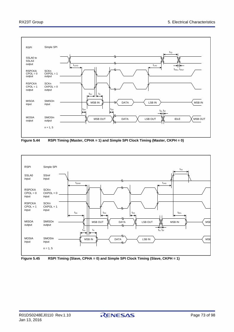
R01DS0248EJ0110 Rev.1.10 Page 73 of 98Jan 13, 2016
RX23T Group 5. Electrical Characteristics
Figure 5.44 RSPI Timing (Master, CPHA = 1) and Simple SPI Clock Timing (Master, CKPH = 0)
Figure 5.45 RSPI Timing (Slave, CPHA = 0) and Simple SPI Clock Timing (Slave, CKPH = 1)
SSLA0 to SSLA3output
RSPCKACPOL = 0output
RSPCKACPOL = 1output
MISOAinput
MOSIAoutput
RSPI Simple SPI
SCKnCKPOL = 1output
SCKnCKPOL = 0output
SMISOninput
SMOSInoutput
tDr, tDf
tSU tH
tLEAD
tTD
tLAG
tSSLr, tSSLf
tOH
MSB IN DATA LSB IN MSB IN
MSB OUT DATA LSB OUT IDLE MSB OUT
tOD
n = 1, 5
tDr, tDftSU tH
tLEAD
tTD
tLAG
tSA
MSB IN DATA LSB IN MSB
MSB OUT DATA LSB OUT MSB IN MSB
tOH tOD tREL
SCKnCKPOL = 0input
SCKnCKPOL = 1input
SMISOnoutput
SMOSIninput
n = 1, 5
Simple SPIRSPI
SSLA0input
RSPCKACPOL = 0input
RSPCKACPOL = 1input
MISOAoutput
MOSIAinput
SSn#input

R01DS0248EJ0110 Rev.1.10 Page 74 of 98Jan 13, 2016
RX23T Group 5. Electrical Characteristics
Figure 5.46 RSPI Timing (Slave, CPHA = 1) and Simple SPI Clock Timing (Slave, CKPH = 0)
Figure 5.47 RIIC Bus Interface Input/Output Timing and Simple I2C Bus Interface Input/Output Timing
tDr, tDf
tSA tOH
tLEAD
tTD
tLAG
tH
LSB OUT(Last data) DATA MSB OUT
MSB IN DATA LSB IN MSB IN
LSB OUT
tSU
tOD tREL
MSB OUT
SCKnCKPOL = 1input
SCKnCKPOL = 0input
SMISOnoutput
SMOSIninput
n = 1, 5
Simple SPIRSPI
SSLA0input
RSPCKACPOL = 0input
RSPCKACPOL = 1input
MISOAoutput
MOSIAinput
SSn#input
Test conditionsVIH = VCC × 0.7, VIL = VCC × 0.3
SDA
SCL
VIH
VIL
tSTAH
tSCLH
tSCLL
P*1 S*1
tSf tSr
tSCLtSDAH
tSDAS
tSTAS tSP tSTOS
P*1
tBUF
Sr*1
Note 1. S, P, and Sr indicate the following conditions, respectively.S: START conditionP: STOP conditionSr: Repeated START condition

R01DS0248EJ0110 Rev.1.10 Page 75 of 98Jan 13, 2016
RX23T Group 5. Electrical Characteristics
5.4 A/D Conversion Characteristics
Note: The characteristics apply when no pin functions other than A/D converter input are used. Absolute accuracy includes quantization errors. Offset error, full-scale error, DNL differential nonlinearity error, and INL integral nonlinearity error do not include quantization errors.
Note 1. The conversion time is the sum of the sampling time and the comparison time. As the test conditions, the number of sampling states is indicated.
Table 5.28 A/D Conversion Characteristics (1)Conditions: VCC = 4.5 V to 5.5 V, AVCC0 = VREFH0 = VCC to 5.5 V, VSS = AVSS0 = VREFL0 = 0 V, Ta = –40 to +105°C
Item Min. Typ. Max. Unit Test Conditions
Frequency 1 — 40 MHz
Resolution — — 12 Bit
Conversion time*1
(Operation at PCLKD = 40 MHz)
Permissible signal source impedance (Max.) = 1.0 kΩSample-and-hold circuit not in use
1.00 — — μs High-precision channelADSSTRn.SST[7:0] bits = 08h
1.25 — — μs Normal-precision channelADSSTRn.SST[7:0] bits = 12h
Permissible signal source impedance (Max.) = 1.0 kΩ / Sample-and-hold circuit in use
1.65 — — μs High-precision channelADSSTRn.SST[7:0] bits = 08hADSHCR.SSTSH[7:0] bits = 0DhAN000 to AN002 = 0.25 V to VREFH0 – 0.25 V
Analog input capacitance — — 12 pF
Offset error — — ±6.5 LSB
Full-scale error — — ±6.5 LSB
Quantization error — ±0.5 — LSB
Absolute accuracy — — ±8.0 LSB
DNL differential nonlinearity error — ±0.5 ±1.5 LSB
INL integral nonlinearity error — ±2.0 ±4.0 LSB

R01DS0248EJ0110 Rev.1.10 Page 76 of 98Jan 13, 2016
RX23T Group 5. Electrical Characteristics
Note: The characteristics apply when no pin functions other than A/D converter input are used. Absolute accuracy includes quantization errors. Offset error, full-scale error, DNL differential nonlinearity error, and INL integral nonlinearity error do not include quantization errors.
Note 1. The conversion time is the sum of the sampling time and the comparison time. As the test conditions, the number of sampling states is indicated.
Note 1. The A/D internal reference voltage indicates the voltage when the internal reference voltage is input to the A/D converter.
Table 5.29 A/D Conversion Characteristics (2)Conditions: VCC = 2.7 V to 5.5 V, AVCC0 = VREFH0 = VCC to 5.5 V, VSS = AVSS0 = VREFL0 = 0 V, Ta = –40 to +105°C
Item Min. Typ. Max. Unit Test Conditions
Frequency 1 — 40 MHz
Resolution — — 12 Bit
Conversion time*1
(Operation at PCLKD = 40 MHz)
Permissible signal source impedance (Max.) = 1.0 kΩSample-and-hold circuit not in use
1.15 — — μs High-precision channelADSSTRn.SST[7:0] bits = 0Eh
1.30 — — μs Normal-precision channelADSSTRn.SST[7:0] bits = 14h
Permissible signal source impedance (Max.) = 1.0 kΩSample-and-hold circuit in use
1.90 — — μs High-precision channel ADSSTRn.SST[7:0] bits = 0Eh ADSHCR.SSTSH[7:0] bits = 11hAN000 to AN002 = 0.25 V to VREFH0 – 0.25 V
Analog input capacitance — — 12 pF
Offset error — — ±6.5 LSB
Full-scale error — — ±6.5 LSB
Quantization error — ±0.5 — LSB
Absolute accuracy — — ±8.0 LSB
DNL differential nonlinearity error — ±0.5 ±1.5 LSB
INL integral nonlinearity error — ±2.0 ±4.0 LSB
Table 5.30 A/D Converter Channel Classification
Classification Channel Conditions Remarks
High-precision channel AN000 to AN007 AVCC0 = 2.7 to 5.5 V Pins AN000 to AN007 cannot be used as digital outputs when the A/D converter is in use.
Normal-precision channel AN016, AN017 VCC = AVCC0 = 2.7 to 5.5 V
Internal reference voltage input channel
Internal reference voltage
AVCC0 = 2.7 to 5.5 V
Table 5.31 A/D Internal Reference Voltage CharacteristicsConditions: VCC = 2.7 V to AVCC0, AVCC0 = VREFH0 = 2.7 V to 5.5 V, VSS = AVSS0 = VREFL0 = 0 V, Ta = –40 to +105°C
Item Min. Typ. Max. Unit Test Conditions
Internal reference voltage input channel*1 1.36 1.43 1.50 V

R01DS0248EJ0110 Rev.1.10 Page 77 of 98Jan 13, 2016
RX23T Group 5. Electrical Characteristics
Figure 5.48 Illustration of A/D Converter Characteristic Terms
Absolute accuracy
Absolute accuracy is the difference between output code based on the theoretical A/D conversion characteristics, and the
actual A/D conversion result. When measuring absolute accuracy, the voltage at the midpoint of the width of analog
input voltage (1-LSB width), that can meet the expectation of outputting an equal code based on the theoretical A/D
conversion characteristics, is used as an analog input voltage. For example, if 12-bit resolution is used and if reference
voltage (VREFH0 = 3.072 V), then 1-LSB width becomes 0.75 mV, and 0 mV, 0.75 mV, 1.5 mV, ... are used as analog
input voltages.
If analog input voltage is 6 mV, absolute accuracy = ±5 LSB means that the actual A/D conversion result is in the range
of 003h to 00Dh though an output code, 008h, can be expected from the theoretical A/D conversion characteristics.
Integral nonlinearity error (INL)
Integral nonlinearity error is the maximum deviation between the ideal line when the measured offset and full-scale
errors are zeroed, and the actual output code.
Integral nonlinearity error (INL)
Actual A/D conversion characteristic
Ideal A/D conversion characteristic
Analog input voltage
Offset error
Absolute accuracy
Differential nonlinearity error (DNL)
Full-scale errorFFFh
000h
0
Ideal line of actual A/D conversion characteristic
1-LSB width for ideal A/D conversion characteristic
Differential nonlinearity error (DNL)
1-LSB width for ideal A/D conversion characteristic
VREFH0(full-scale)
A/D converteroutput code

R01DS0248EJ0110 Rev.1.10 Page 78 of 98Jan 13, 2016
RX23T Group 5. Electrical Characteristics
Differential nonlinearity error (DNL)
Differential nonlinearity error is the difference between 1-LSB width based on the ideal A/D conversion characteristics
and the width of the actual output code.
Offset error
Offset error is the difference between a transition point of the ideal first output code and the actual first output code.
Full-scale error
Full-scale error is the difference between a transition point of the ideal last output code and the actual last output code.
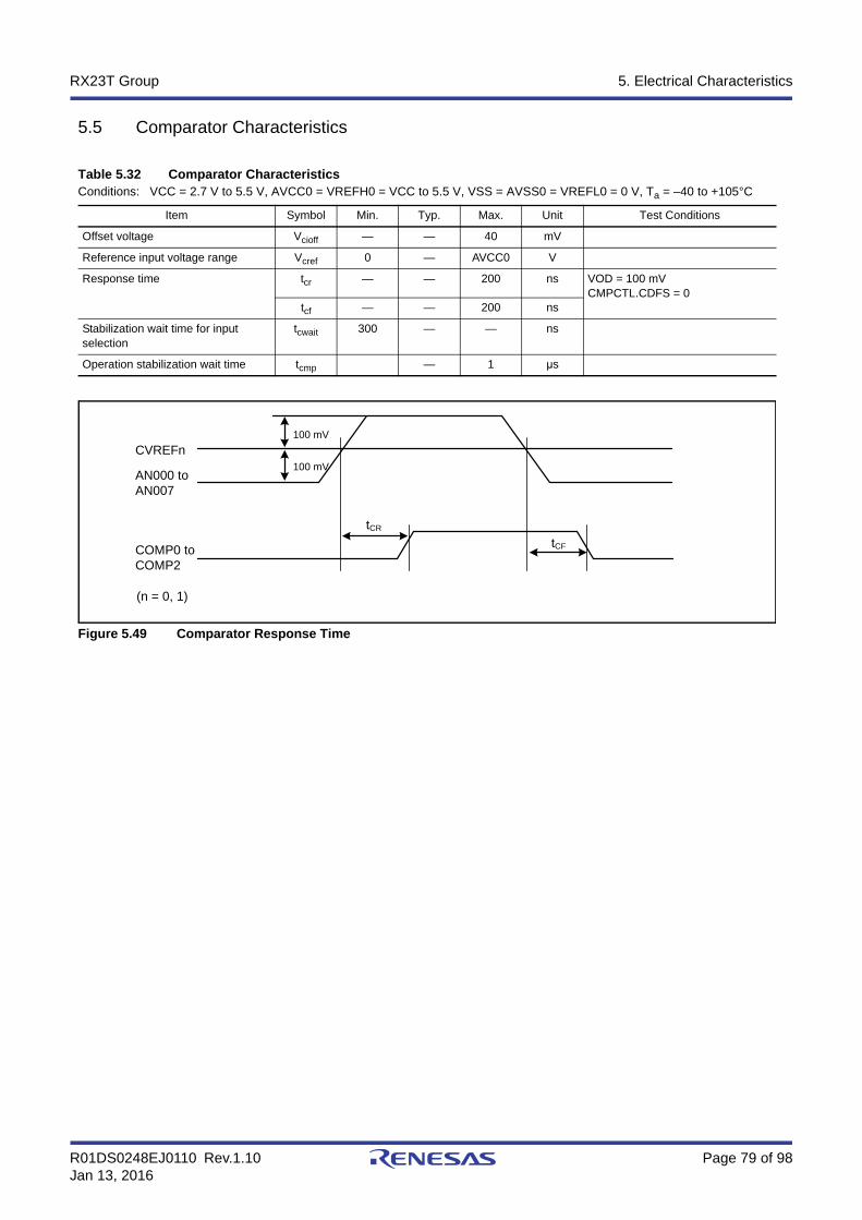
R01DS0248EJ0110 Rev.1.10 Page 79 of 98Jan 13, 2016
RX23T Group 5. Electrical Characteristics
5.5 Comparator Characteristics
Figure 5.49 Comparator Response Time
Table 5.32 Comparator CharacteristicsConditions: VCC = 2.7 V to 5.5 V, AVCC0 = VREFH0 = VCC to 5.5 V, VSS = AVSS0 = VREFL0 = 0 V, Ta = –40 to +105°C
Item Symbol Min. Typ. Max. Unit Test Conditions
Offset voltage Vcioff — — 40 mV
Reference input voltage range Vcref 0 — AVCC0 V
Response time tcr — — 200 ns VOD = 100 mVCMPCTL.CDFS = 0
tcf — — 200 ns
Stabilization wait time for input selection
tcwait 300 — — ns
Operation stabilization wait time tcmp — 1 μs
CVREFn
AN000 to AN007
COMP0 to COMP2
(n = 0, 1)
100 mV
100 mV
tCR
tCF

R01DS0248EJ0110 Rev.1.10 Page 80 of 98Jan 13, 2016
RX23T Group 5. Electrical Characteristics
5.6 D/A Conversion Characteristics
Table 5.33 D/A Conversion CharacteristicsConditions: VCC = 2.7 V to 5.5 V, AVCC0 = VREFH0 = VCC to 5.5 V, VSS = AVSS0 = VREFL0 = 0 V, Ta = –40 to +105°C
Item Symbol Min. Typ. Max. Unit Test Conditions
Resolution — — — 8 Bit
Conversion time tDCONV — — 3.0 μs
Absolute accuracy — — ±1.0 ±3.0 LSB

R01DS0248EJ0110 Rev.1.10 Page 81 of 98Jan 13, 2016
RX23T Group 5. Electrical Characteristics
5.7 Power-On Reset Circuit and Voltage Detection Circuit Characteristics
Note: These characteristics apply when noise is not superimposed on the power supply. When a setting is made so that the voltage detection level overlaps with that of the voltage detection circuit (LVD2), it cannot be specified which of LVD1 and LVD2 is used for voltage detection.
Note 1. n in the symbol Vdet0_n denotes the value of the LVDS0[1:0] bits.Note 2. n in the symbol Vdet1_n denotes the value of the LVDLVLR.LVD1LVL[3:0] bits.Note 3. n in the symbol Vdet2_n denotes the value of the LVDLVLR.LVD2LVL[3:0] bits.
Table 5.34 Power-On Reset Circuit and Voltage Detection Circuit Characteristics (1)Conditions: VCC = 2.7 V to 5.5 V, AVCC0 = VREFH0 = VCC to 5.5 V, VSS = AVSS0 = VREFL0 = 0 V, Ta = –40 to +105°C
Item Symbol Min. Typ. Max. Unit Test Conditions
Voltage detection level
Power-on reset (POR) VPOR 1.35 1.50 1.65 V Figure 5.50, Figure 5.51
Voltage detection circuit (LVD0)*1
Vdet0_0 3.67 3.84 3.97 V
Vdet0_2 2.37 2.51 2.67
Voltage detection circuit (LVD1)*2
Vdet1_0 4.12 4.29 4.42 V Figure 5.53At falling edge VCC
Vdet1_1 3.98 4.14 4.28
Vdet1_2 3.86 4.02 4.16
Vdet1_3 3.68 3.84 3.98
Vdet1_4 2.99 3.10 3.29
Vdet1_5 2.89 3.00 3.19
Vdet1_6 2.79 2.90 3.09
Vdet1_7 2.68 2.79 2.98
Vdet1_8 2.57 2.68 2.87
Voltage detection circuit(LVD2)*1
Vdet2_0*2 4.08 4.29 4.48 Figure 5.54At falling edge VCC
Vdet2_1 3.95 4.14 4.35
Vdet2_2 3.82 4.02 4.22
Vdet2_3 3.62 3.84 4.02
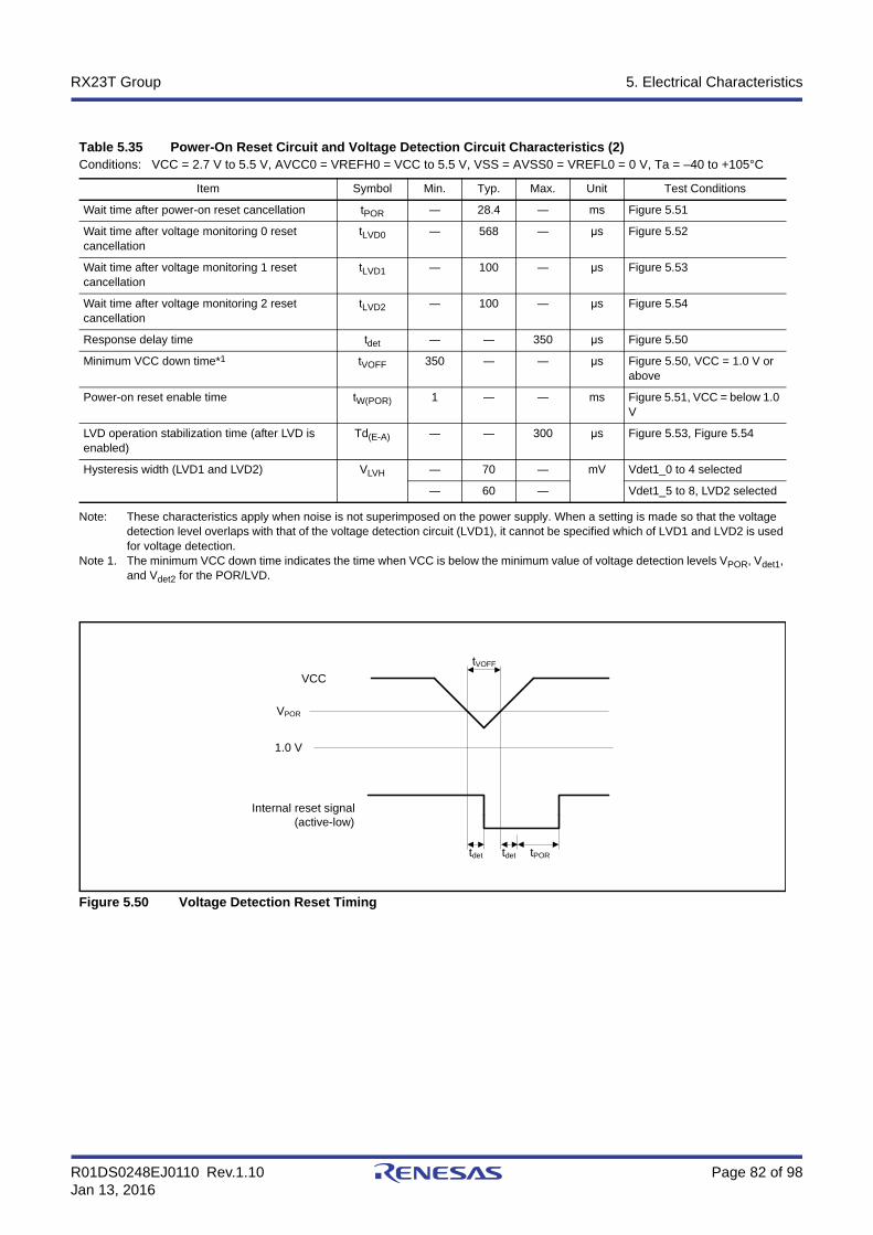
R01DS0248EJ0110 Rev.1.10 Page 82 of 98Jan 13, 2016
RX23T Group 5. Electrical Characteristics
Note: These characteristics apply when noise is not superimposed on the power supply. When a setting is made so that the voltage detection level overlaps with that of the voltage detection circuit (LVD1), it cannot be specified which of LVD1 and LVD2 is used for voltage detection.
Note 1. The minimum VCC down time indicates the time when VCC is below the minimum value of voltage detection levels VPOR, Vdet1, and Vdet2 for the POR/LVD.
Figure 5.50 Voltage Detection Reset Timing
Table 5.35 Power-On Reset Circuit and Voltage Detection Circuit Characteristics (2)Conditions: VCC = 2.7 V to 5.5 V, AVCC0 = VREFH0 = VCC to 5.5 V, VSS = AVSS0 = VREFL0 = 0 V, Ta = –40 to +105°C
Item Symbol Min. Typ. Max. Unit Test Conditions
Wait time after power-on reset cancellation tPOR ― 28.4 ― ms Figure 5.51
Wait time after voltage monitoring 0 reset cancellation
tLVD0 ― 568 ― μs Figure 5.52
Wait time after voltage monitoring 1 reset cancellation
tLVD1 ― 100 ― μs Figure 5.53
Wait time after voltage monitoring 2 reset cancellation
tLVD2 ― 100 ― μs Figure 5.54
Response delay time tdet ― ― 350 μs Figure 5.50
Minimum VCC down time*1 tVOFF 350 ― ― μs Figure 5.50, VCC = 1.0 V or above
Power-on reset enable time tW(POR) 1 ― ― ms Figure 5.51, VCC = below 1.0 V
LVD operation stabilization time (after LVD is enabled)
Td(E-A) ― ― 300 μs Figure 5.53, Figure 5.54
Hysteresis width (LVD1 and LVD2) VLVH ― 70 ― mV Vdet1_0 to 4 selected
― 60 ― Vdet1_5 to 8, LVD2 selected
Internal reset signal(active-low)
VCC
tVOFF
tPORtdet
VPOR
tdet
1.0 V

R01DS0248EJ0110 Rev.1.10 Page 83 of 98Jan 13, 2016
RX23T Group 5. Electrical Characteristics
Figure 5.51 Power-On Reset Timing
Figure 5.52 Voltage Detection Circuit Timing (Vdet0)
Internal reset signal(active-low)
VCC
tPOR
VPOR
1.0 V
tw(POR)
*1
tdet
Note 1. tw(POR) is the time required for a power-on reset to be enabled while the external power VCC is being held below the valid voltage (1.0 V).When VCC turns on, maintain tw(POR) for 1.0 ms or more.
tVOFF
Vdet0VCC
tdettdet
Internal reset signal(active-low)
VLVH
tLVD0
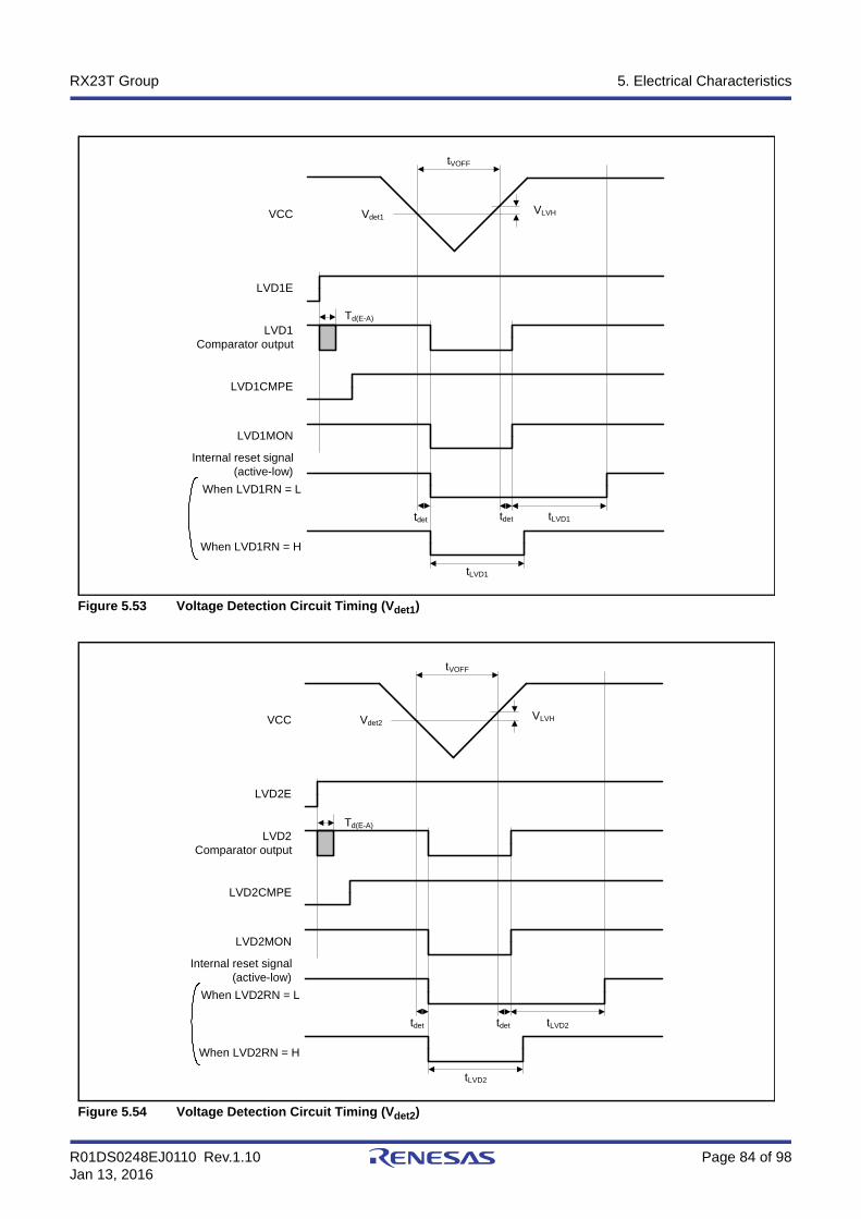
R01DS0248EJ0110 Rev.1.10 Page 84 of 98Jan 13, 2016
RX23T Group 5. Electrical Characteristics
Figure 5.53 Voltage Detection Circuit Timing (Vdet1)
Figure 5.54 Voltage Detection Circuit Timing (Vdet2)
tVOFF
Vdet1VCC
tdettdet
tLVD1
Td(E-A)
LVD1E
LVD1Comparator output
LVD1CMPE
LVD1MON
Internal reset signal(active-low)
When LVD1RN = L
When LVD1RN = H
VLVH
tLVD1
tVOFF
Vdet2VCC
tdettdet
tLVD2
Td(E-A)
LVD2E
LVD2Comparator output
LVD2CMPE
LVD2MON
Internal reset signal (active-low)
When LVD2RN = L
When LVD2RN = H
VLVH
tLVD2

R01DS0248EJ0110 Rev.1.10 Page 85 of 98Jan 13, 2016
RX23T Group 5. Electrical Characteristics
5.8 Oscillation Stop Detection Timing
Figure 5.55 Oscillation Stop Detection Timing
Table 5.36 Oscillation Stop Detection TimingConditions: VCC = 2.7 V to 5.5 V, AVCC0 = VREFH0 = VCC to 5.5 V, VSS = AVSS0 = VREFL0 = 0 V, Ta = –40 to +105°C
Item Symbol Min. Typ. Max. Unit Test Conditions
Detection time tdr — — 1 ms Figure 5.55
tdr
Main clock
OSTDSR.OSTDF
Low-speed clock
ICLK
tdr
Main clock
OSTDSR.OSTDF
ICLK
When the main clock is selectedWhen the PLL clock is selected
PLL clock

R01DS0248EJ0110 Rev.1.10 Page 86 of 98Jan 13, 2016
RX23T Group 5. Electrical Characteristics
5.9 ROM (Flash Memory for Code Storage) Characteristics
Note 1. Definition of reprogram/erase cycle: The reprogram/erase cycle is the number of erasing for each block. When the reprogram/erase cycle is n times (n = 1000), erasing can be performed n times for each block. For instance, when 4-byte programming is performed 256 times for different addresses in 1-Kbyte block and then the entire block is erased, the reprogram/erase cycle is counted as one. However, programming the same address for several times as one erasing is not enabled (overwriting is prohibited).
Note 2. Characteristic when using the flash memory programmer and the self-programming library provided from Renesas Electronics.Note 3. This result is obtained from reliability testing.
Note: Does not include the time until each operation of the flash memory is started after instructions are executed by software.Note: The lower-limit frequency of FCLK is 1 MHz during programming or erasing of the flash memory. When using FCLK at below
4 MHz, the frequency can be set to 1 MHz, 2 MHz, or 3 MHz. A non-integer frequency such as 1.5 MHz cannot be set.Note: The frequency accuracy of FCLK should be ±3.5%.
Table 5.37 ROM (Flash Memory for Code Storage) Characteristics (1)
Item Symbol Min. Typ. Max. Unit Conditions
Reprogramming/erasure cycle*1 NPEC 1000 — — Times
Data hold time After 1000 times of NPEC tDRP 20*2, *3 — — Year Ta = +85°C
Table 5.38 ROM (Flash Memory for Code Storage) Characteristics (2): High-Speed Operating ModeConditions: VCC = 2.7 V to 5.5 V, AVCC0 = VREFH0 = VCC to 5.5 V, VSS = AVSS0 = VREFL0 = 0 V, Ta = –40 to +105°C
Temperature range for the programming/erasure operation: Ta = –40 to +85°C
Item SymbolFCLK = 1 MHz FCLK = 32 MHz
UnitMin. Typ. Max. Min. Typ. Max.
Programming time 8-byte tP8 — 112.0 967.0 — 52.3 490.5 μs
Erasure time 2-Kbyte tE2K — 8.7 278.1 — 5.5 214.6 ms
128-Kbyte (when block erase command used)
— 239.7 5111.4 — 25.9 734.3 ms
128-Kbyte (when all-block erase command used)
tE128K — 234.5 4906.8 — 20.6 524.6 ms
Blank check time 8-byte tBC8 — — 55.0 — — 16.1 μs
2-Kbyte tBC2K — — 1840.0 — — 135.7 μs
Erase operation forcible stop time tSED — — 18.0 — — 10.7 μs
Start-up area switching setting time tSAS — 12.3 566.5 — 6.2 433.5 ms
Access window time tAWS — 12.3 566.5 — 6.2 433.5 ms
ROM mode transition wait time 1 tDIS 2.0 — — 2.0 — — μs
ROM mode transition wait time 2 tMS 5.0 — — 5.0 — — μs
R01DS0248EJ0110 Rev.1.10 Page 87 of 98Jan 13, 2016
RX23T Group 5. Electrical Characteristics
Note: Does not include the time until each operation of the flash memory is started after instructions are executed by software.Note: The lower-limit frequency of FCLK is 1 MHz during programming or erasing of the flash memory. When using FCLK at below
4 MHz, the frequency can be set to 1 MHz, 2 MHz, or 3 MHz. A non-integer frequency such as 1.5 MHz cannot be set.Note: The frequency accuracy of FCLK should be ±3.5%.
Table 5.39 ROM (Flash Memory for Code Storage) Characteristics (3): Middle-Speed Operating ModeConditions: VCC = 2.7 V to 5.5 V, AVCC0 = VREFH0 = VCC to 5.5 V, VSS = AVSS0 = VREFL0 = 0 V, Ta = –40 to +105°C
Temperature range for the programming/erasure operation: Ta = –40 to +85°C
Item SymbolFCLK = 1 MHz FCLK = 8 MHz
UnitMin. Typ. Max. Min. Typ. Max.
Programming time 8-byte tP8 — 152.0 1367.0 — 97.9 936.0 μs
Erasure time 2-Kbyte tE2K — 8.8 279.7 — 5.9 220.8 ms
128-Kbyte (when block erase command used)
— 239.8 5114.7 — 55.5 1336.4 ms
128-Kbyte (when all-block erase command used)
tE128K — 234.6 4908.5 — 50.3 1130.1 ms
Blank check time 8-byte tBC8 — — 85.0 — — 50.9 μs
2-Kbyte tBC2K — — 1870.0 — — 401.5 μs
Erase operation forcible stop time tSED — — 28.0 — — 21.3 μs
Start-up area switching setting time tSAS — 13.0 573.3 — 7.7 450.1 ms
Access window time tAWS — 13.0 573.3 — 7.7 450.1 ms
ROM mode transition wait time 1 tDIS 2.0 — — 2.0 — — μs
ROM mode transition wait time 2 tMS 3.0 — — 3.0 — — μs

R01DS0248EJ0110 Rev.1.10 Page 88 of 98Jan 13, 2016
RX23T Group 5. Electrical Characteristics
5.10 Usage Notes
5.10.1 Connecting VCL Capacitor and Bypass Capacitors
This MCU integrates an internal voltage-down circuit, which is used for lowering the power supply voltage in the
internal MCU to adjust automatically to the optimum level. A 4.7-μF capacitor needs to be connected between this
internal voltage-down power supply (VCL pin) and VSS pin. Figure 5.56 to Figure 5.58 shows how to connect
external capacitors. Place an external capacitor close to the pins. Do not apply the power supply voltage to the VCL pin.
Insert a multilayer ceramic capacitor as a bypass capacitor between each pair of the power supply pins. Implement a
bypass capacitor to the MCU power supply pins as close as possible. Use a recommended value of 0.1 μF as the
capacitance of the capacitors. For the capacitors related to crystal oscillation, see section 9, Clock Generation Circuit
in the User’s Manual: Hardware. For the capacitors related to analog modules, also see section 29, 12-Bit A/D
Converter (S12ADE) in the User’s Manual: Hardware.
For notes on designing the printed circuit board, see the descriptions of the application note "Hardware Design Guide"
(R01AN1411EJ). The latest version can be downloaded from Renesas Electronics Website.

R01DS0248EJ0110 Rev.1.10 Page 89 of 98Jan 13, 2016
RX23T Group 5. Electrical Characteristics
Figure 5.56 Connecting Capacitors (64 Pins)
48 47 46 45 44 43 42 41 40 39 38 37 36 35 34 33
32
31
30
29
28
27
26
25
24
23
22
21
20
19
18
17
1 2 3 4 5 6 7 8 9 10 11 12 13 14 15 16
54
55
51
49
50
52
53
56
57
58
59
60
61
63
64
62
RX23T GroupPLQP0064KB-C(64-pin LQFP)
(Top view)
VS
S
VC
C
VSS
VCC
VC
L
VS
S
VC
C
External capacitor for power supply stabilization4.7 µF
Bypass capacitor0.1 µF
Bypass capacitor0.1 µF
Bypass capacitor0.1 µF
Note 1. Do not apply the power supply voltage to the VCL pin .Note 2. Use a 4.7-µF multilayer ceramic for the VCL pin and place it close to the pin .
A recommended value is shown for the capacitance of the bypass capacitors .
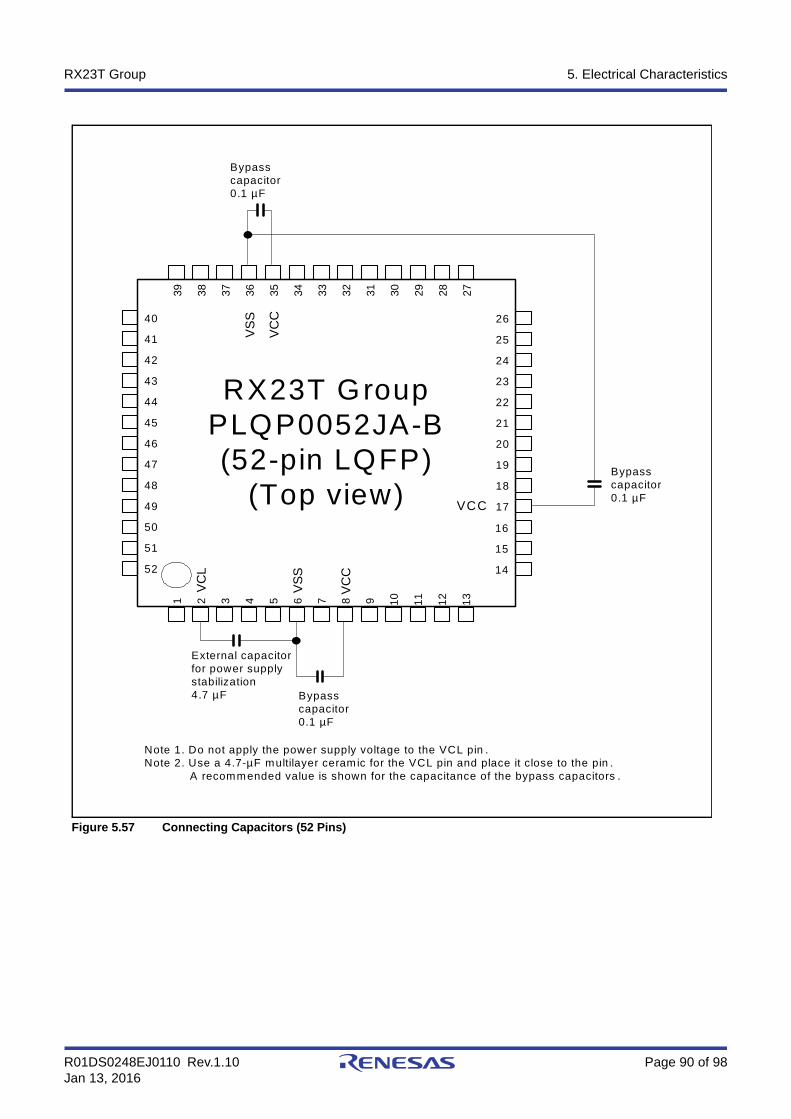
R01DS0248EJ0110 Rev.1.10 Page 90 of 98Jan 13, 2016
RX23T Group 5. Electrical Characteristics
Figure 5.57 Connecting Capacitors (52 Pins)
39 38 37 36 35 34 33 32 31 30 29 28 27
26
25
24
23
22
21
20
19
18
17
1 2 3 4 5 6 7 8 9 10
11
12
13
45
46
42
40
41
43
44
47
48
49
50
51
52
RX23T GroupPLQP0052JA-B(52-pin LQFP)
(Top view)
VS
S
VC
C
VCC
VC
L
VS
S
VC
C
16
15
14
Bypass capacitor0.1 µF
External capacitor for power supply stabilization4.7 µF Bypass
capacitor0.1 µF
Bypass capacitor0.1 µF
Note 1. Do not apply the power supply voltage to the VCL pin .Note 2. Use a 4.7-µF multilayer ceramic for the VCL pin and place it close to the pin .
A recommended value is shown for the capacitance of the bypass capacitors .
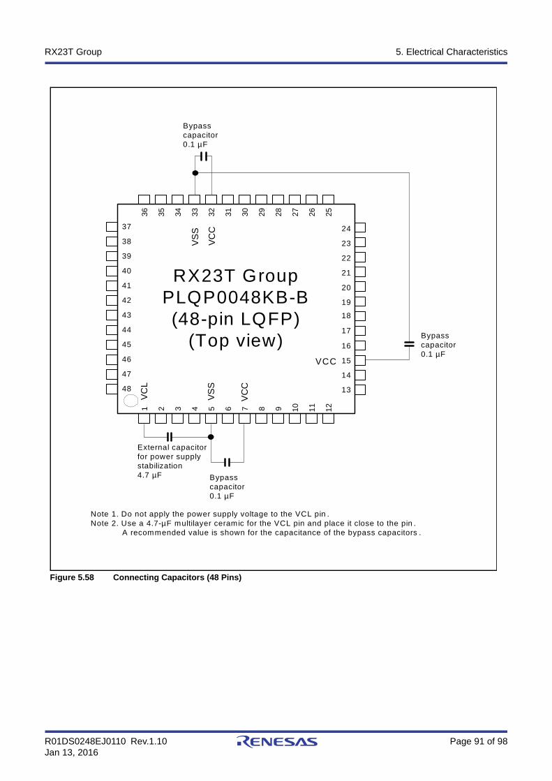
R01DS0248EJ0110 Rev.1.10 Page 91 of 98Jan 13, 2016
RX23T Group 5. Electrical Characteristics
Figure 5.58 Connecting Capacitors (48 Pins)
36 35 34 33 32 31 30 29 28 27 26 25
24
23
22
21
20
19
1 2 3 4 5 6 7 8 9 10 11 12
38
39
37
40
41
42
43
44
45
47
48
46
RX23T GroupPLQP0048KB-B(48-pin LQFP)
(Top view)
VS
S
VC
C
VCC
VC
L
VS
S
VC
C
18
17
16
15
14
13
Bypass capacitor0.1 µF
Bypass capacitor0.1 µF
External capacitor for power supply stabilization4.7 µF Bypass
capacitor0.1 µF
Note 1. Do not apply the power supply voltage to the VCL pin .Note 2. Use a 4.7-µF multilayer ceramic for the VCL pin and place it close to the pin .
A recommended value is shown for the capacitance of the bypass capacitors .
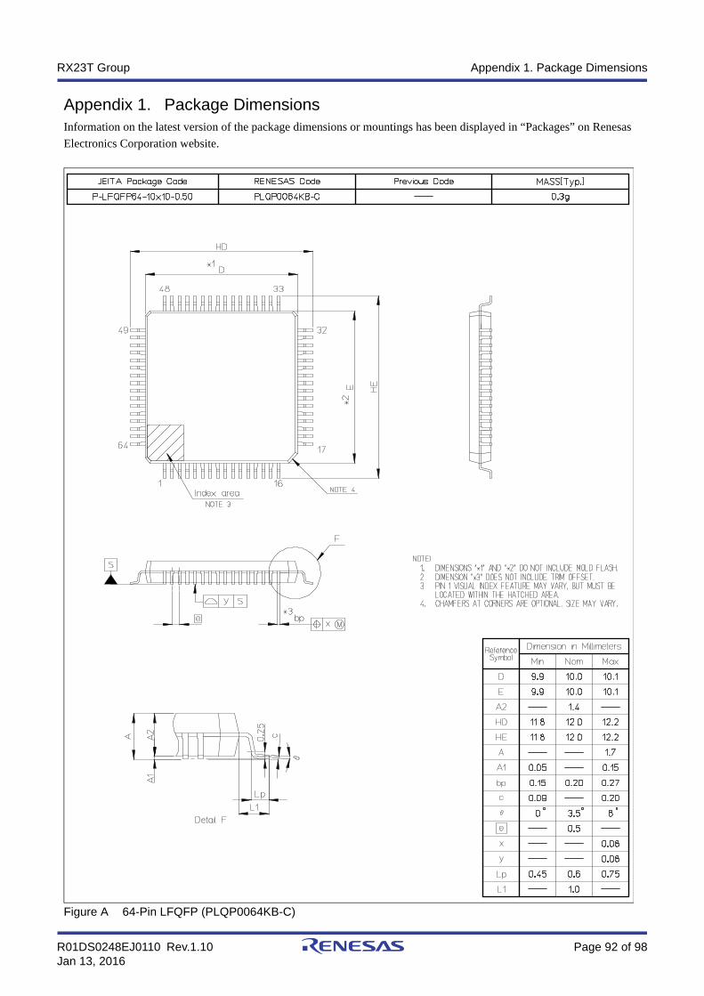
R01DS0248EJ0110 Rev.1.10 Page 92 of 98Jan 13, 2016
RX23T Group Appendix 1. Package Dimensions
Appendix 1. Package DimensionsInformation on the latest version of the package dimensions or mountings has been displayed in “Packages” on Renesas
Electronics Corporation website.
Figure A 64-Pin LFQFP (PLQP0064KB-C)

R01DS0248EJ0110 Rev.1.10 Page 93 of 98Jan 13, 2016
RX23T Group Appendix 1. Package Dimensions
Figure B 52-Pin LQFP (PLQP0052JA-B)
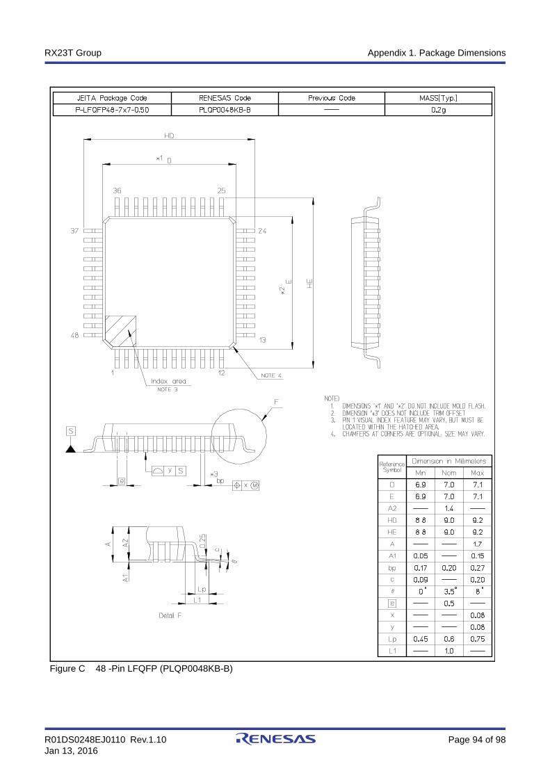
R01DS0248EJ0110 Rev.1.10 Page 94 of 98Jan 13, 2016
RX23T Group Appendix 1. Package Dimensions
Figure C 48 -Pin LFQFP (PLQP0048KB-B)

R01DS0248EJ0110 Rev.1.10 Page 95 of 98Jan 13, 2016
RX23T Group REVISION HISTORY
Classifications
- Items with Technical Update document number: Changes according to the corresponding issued Technical Update
- Items without Technical Update document number: Minor changes that do not require Technical Update to be issued
REVISION HISTORY RX23T Group Datasheet
Rev. DateDescription
ClassificationPage Summary
1.00 Mar 31, 2015 — First edition, issued
1.10 Oct 30, 2015 Features
1 Features changed
1. Overview
2, 3 Table 1.1 Outline of Specifications (1/3) (2/3) changed
6 Table 1.3 List of Products: D Version (Ta = –40 to +85°C) changed
6 Table 1.4 List of Products: G Version (Ta = –40 to +105°C) changed
7 Figure 1.1 How to Read the Product Part Number changed
10 Table 1.5 Pin Functions (2/2) changed
11 Figure 1.3 Pin Assignments of the 64-Pin LFQFP changed
12 Figure 1.4 Pin Assignments of the 52-Pin LQFP changed
13 Figure 1.5 Pin Assignments of the 48-Pin LFQFP changed
14 Table 1.6 List of Pins and Pin Functions (64-Pin LFQFP) (1/2) changed
16 Table 1.7 List of Pins and Pin Functions (52-Pin LQFP) changed
17 Table 1.8 List of Pins and Pin Functions (48-Pin LFQFP) changed
3. Address Space
22 Figure 3.1 Memory Map in Each Operating Mode changed
4. I/O Registers
25 Table 4.1 List of I/O Registers (Address Order) (1 / 16)Address: 0008 0036h High-Speed On-Chip Oscillator Control Register (HOCOCR), Address: 0008 00A5h High-Speed On-Chip Oscillator Wait Control Register (HOCOWTCR) added
34 Table 4.1 List of I/O Registers (Address Order) (10 / 16)Address: 0008 C087h Open Drain Control Register 1 (ODR1) added
5. Electrical Characteristics
42 Table 5.3 DC Characteristics (1) changed
57 Table 5.14 Operating Frequency Value (High-Speed Operating Mode), Table 5.15 Operating Frequency Value (Middle-Speed Operating Mode) changed
58 Table 5.16 Clock Timing, Figure 5.20 EXTAL External Clock Input Timing changed
59, 60 Figure 5.24 HOCO Clock Oscillation Start Timing (After Reset is Canceled by Setting OFS1.HOCOEN Bit to 0), Figure 5.25 HOCO Clock Oscillation Start Timing (Oscillation is Started by Setting HOCOCR.HCSTP Bit) added
79 Table 5.32 Comparator Characteristics changed
80 Table 5.33 D/A Conversion Characteristics symbol added
82 Table 5.35 Power-On Reset Circuit and Voltage Detection Circuit Characteristics (2) changed
83 Figure 5.52 Voltage Detection Circuit Timing (Vdet0) changed
89 Figure 5.56 Connecting Capacitors (64 Pins) changed
90 Figure 5.57 Connecting Capacitors (52 Pins) changed
91 Figure 5.58 Connecting Capacitors (48 Pins) changed
Appendix 1. Package Dimensions
92 Figure A 64-Pin LFQFP (PLQP0064KB-C) changed
93 Figure B 52-Pin LQFP (PLQP0052JA-B) changed
94 Figure C 48 -Pin LFQFP (PLQP0048KB-B) changed
REVISION HISTORY
NOTES FOR CMOS DEVICES
(1) VOLTAGE APPLICATION WAVEFORM AT INPUT PIN: Waveform distortion due to input noise or a
reflected wave may cause malfunction. If the input of the CMOS device stays in the area between VIL (MAX) and VIH (MIN) due to noise, etc., the device may malfunction. Take care to prevent chattering noise from entering the device when the input level is fixed, and also in the transition period when the input level passes through the area between VIL (MAX) and VIH (MIN).
(2) HANDLING OF UNUSED INPUT PINS: Unconnected CMOS device inputs can be cause of malfunction. If an input pin is unconnected, it is possible that an internal input level may be generated due to noise, etc., causing malfunction. CMOS devices behave differently than Bipolar or NMOS devices. Input levels of CMOS devices must be fixed high or low by using pull-up or pull-down circuitry. Each unused pin should be connected to VDD or GND via a resistor if there is a possibility that it will be an output pin. All handling related to unused pins must be judged separately for each device and according to related specifications governing the device.
(3) PRECAUTION AGAINST ESD: A strong electric field, when exposed to a MOS device, can cause destruction of the gate oxide and ultimately degrade the device operation. Steps must be taken to stop generation of static electricity as much as possible, and quickly dissipate it when it has occurred. Environmental control must be adequate. When it is dry, a humidifier should be used. It is recommended to avoid using insulators that easily build up static electricity. Semiconductor devices must be stored and transported in an anti-static container, static shielding bag or conductive material. All test and measurement tools including work benches and floors should be grounded. The operator should be grounded using a wrist strap. Semiconductor devices must not be touched with bare hands. Similar precautions need to be taken for PW boards with mounted semiconductor devices.
(4) STATUS BEFORE INITIALIZATION: Power-on does not necessarily define the initial status of a MOS device. Immediately after the power source is turned ON, devices with reset functions have not yet been initialized. Hence, power-on does not guarantee output pin levels, I/O settings or contents of registers. A device is not initialized until the reset signal is received. A reset operation must be executed immediately after power-on for devices with reset functions.
(5) POWER ON/OFF SEQUENCE: In the case of a device that uses different power supplies for the internal operation and external interface, as a rule, switch on the external power supply after switching on the internal power supply. When switching the power supply off, as a rule, switch off the external power supply and then the internal power supply. Use of the reverse power on/off sequences may result in the application of an overvoltage to the internal elements of the device, causing malfunction and degradation of internal elements due to the passage of an abnormal current. The correct power on/off sequence must be judged separately for each device and according to related specifications governing the device.
(6) INPUT OF SIGNAL DURING POWER OFF STATE : Do not input signals or an I/O pull-up power supply while the device is not powered. The current injection that results from input of such a signal or I/O pull-up power supply may cause malfunction and the abnormal current that passes in the device at this time may cause degradation of internal elements. Input of signals during the power off state must be judged separately for each device and according to related specifications governing the device.

General Precautions in the Handling of MPU/MCU Products The following usage notes are applicable to all MPU/MCU products from Renesas. For detailed usage notes on the products covered by this document, refer to the relevant sections of the document as well as any technical updates that have been issued for the products.
1. Handling of Unused Pins Handle unused pins in accord with the directions given under Handling of Unused Pins in the manual. ⎯ The input pins of CMOS products are generally in the high-impedance state. In operation with an
unused pin in the open-circuit state, extra electromagnetic noise is induced in the vicinity of LSI, an associated shoot-through current flows internally, and malfunctions occur due to the false recognition of the pin state as an input signal become possible. Unused pins should be handled as described under Handling of Unused Pins in the manual.
2. Processing at Power-on The state of the product is undefined at the moment when power is supplied. ⎯ The states of internal circuits in the LSI are indeterminate and the states of register settings and
pins are undefined at the moment when power is supplied. In a finished product where the reset signal is applied to the external reset pin, the states of pins are not guaranteed from the moment when power is supplied until the reset process is completed. In a similar way, the states of pins in a product that is reset by an on-chip power-on reset function are not guaranteed from the moment when power is supplied until the power reaches the level at which resetting has been specified.
3. Prohibition of Access to Reserved Addresses Access to reserved addresses is prohibited. ⎯ The reserved addresses are provided for the possible future expansion of functions. Do not access
these addresses; the correct operation of LSI is not guaranteed if they are accessed. 4. Clock Signals
After applying a reset, only release the reset line after the operating clock signal has become stable. When switching the clock signal during program execution, wait until the target clock signal has stabilized. ⎯ When the clock signal is generated with an external resonator (or from an external oscillator)
during a reset, ensure that the reset line is only released after full stabilization of the clock signal. Moreover, when switching to a clock signal produced with an external resonator (or by an external oscillator) while program execution is in progress, wait until the target clock signal is stable.
5. Differences between Products Before changing from one product to another, i.e. to a product with a different part number, confirm that the change will not lead to problems. ⎯ The characteristics of an MPU or MCU in the same group but having a different part number may
differ in terms of the internal memory capacity, layout pattern, and other factors, which can affect the ranges of electrical characteristics, such as characteristic values, operating margins, immunity to noise, and amount of radiated noise. When changing to a product with a different part number, implement a system-evaluation test for the given product.
Notice1. Descriptions of circuits, software and other related information in this document are provided only to illustrate the operation of semiconductor products and application examples. You are fully responsible for
the incorporation of these circuits, software, and information in the design of your equipment. Renesas Electronics assumes no responsibility for any losses incurred by you or third parties arising from the
use of these circuits, software, or information.
2. Renesas Electronics has used reasonable care in preparing the information included in this document, but Renesas Electronics does not warrant that such information is error free. Renesas Electronics
assumes no liability whatsoever for any damages incurred by you resulting from errors in or omissions from the information included herein.
3. Renesas Electronics does not assume any liability for infringement of patents, copyrights, or other intellectual property rights of third parties by or arising from the use of Renesas Electronics products or
technical information described in this document. No license, express, implied or otherwise, is granted hereby under any patents, copyrights or other intellectual property rights of Renesas Electronics or
others.
4. You should not alter, modify, copy, or otherwise misappropriate any Renesas Electronics product, whether in whole or in part. Renesas Electronics assumes no responsibility for any losses incurred by you or
third parties arising from such alteration, modification, copy or otherwise misappropriation of Renesas Electronics product.
5. Renesas Electronics products are classified according to the following two quality grades: "Standard" and "High Quality". The recommended applications for each Renesas Electronics product depends on
the product's quality grade, as indicated below.
"Standard": Computers; office equipment; communications equipment; test and measurement equipment; audio and visual equipment; home electronic appliances; machine tools; personal electronic
equipment; and industrial robots etc.
"High Quality": Transportation equipment (automobiles, trains, ships, etc.); traffic control systems; anti-disaster systems; anti-crime systems; and safety equipment etc.
Renesas Electronics products are neither intended nor authorized for use in products or systems that may pose a direct threat to human life or bodily injury (artificial life support devices or systems, surgical
implantations etc.), or may cause serious property damages (nuclear reactor control systems, military equipment etc.). You must check the quality grade of each Renesas Electronics product before using it
in a particular application. You may not use any Renesas Electronics product for any application for which it is not intended. Renesas Electronics shall not be in any way liable for any damages or losses
incurred by you or third parties arising from the use of any Renesas Electronics product for which the product is not intended by Renesas Electronics.
6. You should use the Renesas Electronics products described in this document within the range specified by Renesas Electronics, especially with respect to the maximum rating, operating supply voltage
range, movement power voltage range, heat radiation characteristics, installation and other product characteristics. Renesas Electronics shall have no liability for malfunctions or damages arising out of the
use of Renesas Electronics products beyond such specified ranges.
7. Although Renesas Electronics endeavors to improve the quality and reliability of its products, semiconductor products have specific characteristics such as the occurrence of failure at a certain rate and
malfunctions under certain use conditions. Further, Renesas Electronics products are not subject to radiation resistance design. Please be sure to implement safety measures to guard them against the
possibility of physical injury, and injury or damage caused by fire in the event of the failure of a Renesas Electronics product, such as safety design for hardware and software including but not limited to
redundancy, fire control and malfunction prevention, appropriate treatment for aging degradation or any other appropriate measures. Because the evaluation of microcomputer software alone is very difficult,
please evaluate the safety of the final products or systems manufactured by you.
8. Please contact a Renesas Electronics sales office for details as to environmental matters such as the environmental compatibility of each Renesas Electronics product. Please use Renesas Electronics
products in compliance with all applicable laws and regulations that regulate the inclusion or use of controlled substances, including without limitation, the EU RoHS Directive. Renesas Electronics assumes
no liability for damages or losses occurring as a result of your noncompliance with applicable laws and regulations.
9. Renesas Electronics products and technology may not be used for or incorporated into any products or systems whose manufacture, use, or sale is prohibited under any applicable domestic or foreign laws or
regulations. You should not use Renesas Electronics products or technology described in this document for any purpose relating to military applications or use by the military, including but not limited to the
development of weapons of mass destruction. When exporting the Renesas Electronics products or technology described in this document, you should comply with the applicable export control laws and
regulations and follow the procedures required by such laws and regulations.
10. It is the responsibility of the buyer or distributor of Renesas Electronics products, who distributes, disposes of, or otherwise places the product with a third party, to notify such third party in advance of the
contents and conditions set forth in this document, Renesas Electronics assumes no responsibility for any losses incurred by you or third parties as a result of unauthorized use of Renesas Electronics
products.
11. This document may not be reproduced or duplicated in any form, in whole or in part, without prior written consent of Renesas Electronics.
12. Please contact a Renesas Electronics sales office if you have any questions regarding the information contained in this document or Renesas Electronics products, or if you have any other inquiries.
(Note 1) "Renesas Electronics" as used in this document means Renesas Electronics Corporation and also includes its majority-owned subsidiaries.
(Note 2) "Renesas Electronics product(s)" means any product developed or manufactured by or for Renesas Electronics.
http://www.renesas.comRefer to "http://www.renesas.com/" for the latest and detailed information.
Renesas Electronics America Inc.2801 Scott Boulevard Santa Clara, CA 95050-2549, U.S.A.Tel: +1-408-588-6000, Fax: +1-408-588-6130
Renesas Electronics Canada Limited9251 Yonge Street, Suite 8309 Richmond Hill, Ontario Canada L4C 9T3Tel: +1-905-237-2004
Renesas Electronics Europe LimitedDukes Meadow, Millboard Road, Bourne End, Buckinghamshire, SL8 5FH, U.KTel: +44-1628-585-100, Fax: +44-1628-585-900
Renesas Electronics Europe GmbHArcadiastrasse 10, 40472 Düsseldorf, Germany Tel: +49-211-6503-0, Fax: +49-211-6503-1327
Renesas Electronics (China) Co., Ltd.Room 1709, Quantum Plaza, No.27 ZhiChunLu Haidian District, Beijing 100191, P.R.ChinaTel: +86-10-8235-1155, Fax: +86-10-8235-7679
Renesas Electronics (Shanghai) Co., Ltd.Unit 301, Tower A, Central Towers, 555 Langao Road, Putuo District, Shanghai, P. R. China 200333 Tel: +86-21-2226-0888, Fax: +86-21-2226-0999
Renesas Electronics Hong Kong LimitedUnit 1601-1611, 16/F., Tower 2, Grand Century Place, 193 Prince Edward Road West, Mongkok, Kowloon, Hong KongTel: +852-2265-6688, Fax: +852 2886-9022
Renesas Electronics Taiwan Co., Ltd.13F, No. 363, Fu Shing North Road, Taipei 10543, TaiwanTel: +886-2-8175-9600, Fax: +886 2-8175-9670
Renesas Electronics Singapore Pte. Ltd.80 Bendemeer Road, Unit #06-02 Hyflux Innovation Centre, Singapore 339949Tel: +65-6213-0200, Fax: +65-6213-0300
Renesas Electronics Malaysia Sdn.Bhd.Unit 1207, Block B, Menara Amcorp, Amcorp Trade Centre, No. 18, Jln Persiaran Barat, 46050 Petaling Jaya, Selangor Darul Ehsan, MalaysiaTel: +60-3-7955-9390, Fax: +60-3-7955-9510
Renesas Electronics India Pvt. Ltd.No.777C, 100 Feet Road, HAL II Stage, Indiranagar, Bangalore, IndiaTel: +91-80-67208700, Fax: +91-80-67208777
Renesas Electronics Korea Co., Ltd.12F., 234 Teheran-ro, Gangnam-Gu, Seoul, 135-080, KoreaTel: +82-2-558-3737, Fax: +82-2-558-5141
SALES OFFICES
© 2016 Renesas Electronics Corporation. All rights reserved.
Colophon 5.0