rw1092 v1.3 100909 - newhaven display international, inc. · rw1092 revision history version date...
TRANSCRIPT

Rev1.4-13 Sep 2010 1
Dot Matrix Type LCD Controller RW1092
FEATURES Direct display of RAM data through the display data
RAM. RAM capacity:192 x 97 = 18624bits Display duty selectable by hardware 1/97 duty: 97common x 160segment
1/65 duty: 65common x 192segment 1/33 duty: 33common x 192segment 1/17 duty: 17common x 192segment
1/9 duty: 9 common x 192segment 1/5 duty: 5 common x 192segment Static : 1 common x 192segment
Both 6800 and 8080 series MPU can directly
connected by 8-bit parallel interface, also 4 line / 3 line serial interface and IIC interface are supportable.
Abundant command functions Low-power liquid crystal display power supply circuit
equipped internally. Bias set 1/2 1/3 1/4 1/5 1/6 1/7 1/8 1/9 1/10 by
software Booster circuit (with Boost ratios of
2X/3X/4X/5X/6X/7X,
where the step-up voltage reference power supply can be input externally). V0 voltage regulator resistors equipped internally, V1 to VSS voltage divider resistors equipped internally, electronic volume function equipped internally, voltage follower
CR oscillator circuit equipped internally (external clock can also be input)
Low power consumption. Logic power supply VDD – VSS = 1.8V to 3.6 V Boost reference voltage: VDD2 – VSS = 2.4V to 3.6V Booster maximum voltage limited VOUT=18.0V Liquid crystal drive power supply: V0 – VSS = 5.0V to 14.0 V
Wide range of operating temperatures: –40 to 85°C CMOS process Shipping forms include bare chip and COG. Software compatible to
SED1065/SED1565/SED1575 Static Display function support
GENERAL DESCRIPTION The RW1092 is a single-chip dot matrix LCD driver that can be connected directly to a microprocessor bus. 8-bit parallel or serial display data sent from the microprocessor is stored in the internal display data RAM and the chip generates a LCD drive signal independent of the microprocessor. Because the chips in the RW1092 contain 97x192 bits of display data RAM and there is a 1-to-1 correspondence between the LCD panel pixels and the internal RAM bits, these chips enable displays with a high degree of freedom.
The chips are able to minimize power consumption because no external operating clock is necessary for the display data RAM read/write operation. Furthermore, because each chip is equipped internally with a low-power LCD driver power supply, and a display clock CR oscillator circuit, the RW1092 can be used to create the lowest power display system with the fewest components for High-performance portable devices.
PART NO. VRS temperature gradient VRS range RW1092 -0.05%/°C 2.1V ±0.03V

Rev1.4-13 Sep 2010 2
Dot Matrix Type LCD Controller RW1092
RW1092 Revision History
Version Date Description
1.0 2010/01/04 AAdddd ssttaattiicc oonn FFuunnccttiioonn 、、AAdddd 33SSPPII ddaattaa lleennggtthh ccoommmmaanndd、、NN--lliinnee RReevveerrssaall FFuunnccttiioonn vvaalliidd ffoorr aallll mmooddee
1.1 2010/05/18 Add application circuit and static application note, modify the
chip thickness to 500um
1.2 2010/07/12 Add external RA、RB use command and Frame frequency
adjustment command
1.3 2010/08/12
Make correction for numbers of duty.
P.1, P.4 ~P.9, P.10 ~ P.15, P.16 ~ P.21, P.22~ P.27,
P.28 ~ P.33, P.34 ~ P.39, P.43, P.44, P.48, P.49
1.4 2010/9/13 Modify Power of sequence

Rev1.4-13 Sep 2010 3
Dot Matrix Type LCD Controller RW1092
PAD ARRANGEMENT Chip Size: 6,294μm x 1,074 μm Min. Bump Pitch: 30μm(Min.) Bump Size: PAD No. 001~009 22.4μm x 81μm PAD No. 010~104 35μm x 52μm PAD No. 105~113 22.4μm x 81μm PAD No. 114~138 81μm x 22.4μm
PAD No. 139~328 15μm x 124μm PAD No. 329~353 81μm x 22.4μm Bump Height: 15μm(Typ) Chip Thickness: 500 μm
114 138
105 113
10 104
1 9
353 329
328 139
(-2468.73,296.79)
30μm
60μm
15μm
15μm
15μm 28μm 15μm
60μm
30μm
30μm 15μm
15μm
45μm (2870.19, 166.47)
( 0, 0 )

Rev1.4-13 Sep 2010 4
Dot Matrix Type LCD Controller RW1092
PAD Coordinate(1/97 Duty, SHL=0,3-1) Pad No. Pad Name X Y Pad No.
Pad
Name X Y Pad No. Pad Name X Y
1 COM[88] 2843.23 445 41 VOUT 843.94 459.4 81 T[7] -1197.58 459.4
2 COM[89] 2805.83 445 42 VOUT 793.94 459.4 82 T[6] -1247.58 459.4
3 COM[90] 2768.43 445 43 VOUT 743.94 459.4 83 T[5] -1297.58 459.4
4 COM[91] 2731.03 445 44 VOUT 693.94 459.4 84 T[4] -1347.58 459.4
5 COM[92] 2693.63 445 45 CAP5P 637.84 459.4 85 T[3] -1397.58 459.4
6 COM[93] 2656.23 445 46 CAP5P 587.84 459.4 86 T[2] -1447.58 459.4
7 COM[94] 2618.83 445 47 CAP1N 537.84 459.4 87 T[1] -1497.58 459.4
8 COM[95] 2581.43 445 48 CAP1N 487.84 459.4 88 T[0] -1547.58 459.4
9 COMS1 2544.03 445 49 CAP3P 437.84 459.4 89 VDD -1599.67 459.4
10 STACOM 2424.72 459.4 50 CAP3P 387.84 459.4 90 CLS -1653.75 459.4
11 VSS 2370.61 459.4 51 CAP1N 337.84 459.4 91 VSS -1705.84 459.4
12 CS1B 2318.55 459.4 52 CAP1N 287.84 459.4 92 C86 -1759.92 459.4
13 CS2 2268.55 459.4 53 CAP1P 237.84 459.4 93 VDD -1812.01 459.4
14 VDD 2214.47 459.4 54 CAP1P 187.84 459.4 94 PSB -1866.09 459.4
15 RSTP 2162.38 459.4 55 CAP2P 137.84 459.4 95 VSS -1918.18 459.4
16 A0 2112.38 459.4 56 CAP2P 87.84 459.4 96 IRS -1972.26 459.4
17 VSS 2058.3 459.4 57 CAP2N 37.84 459.4 97 VDD -2024.35 459.4
18 RW(XWR) 2006.21 459.4 58 CAP2N -12.16 459.4 98 SEL1 -2078.43 459.4
19 E(XRD) 1956.21 459.4 59 CAP4P -62.16 459.4 99 VSS -2130.52 459.4
20 VDD 1902.13 459.4 60 CAP4P -112.16 459.4 100 SEL2 -2184.6 459.4
21 D0 1850.04 459.4 61 CAP2N -162.16 459.4 101 VDD -2236.69 459.4
22 D1 1800.04 459.4 62 CAP2N -212.16 459.4 102 SEL3 -2290.77 459.4
23 D2 1750.04 459.4 63 CAP6P -262.16 459.4 103 VSS -2340.77 459.4
24 D3 1700.04 459.4 64 CAP6P -312.16 459.4 104 V0 -2396.87 459.4
25 D4 1650.04 459.4 65 VSS -371.7 459.4 105 COM[47] -2544.03 445
26 D5 1600.04 459.4 66 VRS -424.72 459.4 106 COM[46] -2581.43 445
27 D6 1550.04 459.4 67 VDD -477.72 459.4 107 COM[45] -2618.83 445
28 D7 1500.04 459.4 68 V4 -535.04 459.4 108 COM[44] -2656.23 445
29 VDD 1450.04 459.4 69 V4 -585.04 459.4 109 COM[43] -2693.63 445
30 VDD 1400.04 459.4 70 V3 -635.04 459.4 110 COM[42] -2731.03 445
31 VDD 1350.04 459.4 71 V3 -685.04 459.4 111 COM[41] -2768.43 445
32 VDD 1300.04 459.4 72 V2 -735.04 459.4 112 COM[40] -2805.83 445
33 VDD2 1250.04 459.4 73 V2 -785.04 459.4 113 COM[39] -2843.23 445
34 VDD2 1200.04 459.4 74 V1 -835.04 459.4 114 COM[38] -3055 449.1
35 VDD2 1150.04 459.4 75 V1 -885.04 459.4 115 COM[37] -3055 411.7
36 VDD2 1100.04 459.4 76 V0 -935.04 459.4 116 COM[36] -3055 374.3
37 VSS 1050.04 459.4 77 V0 -985.04 459.4 117 COM[35] -3055 336.9
38 VSS 1000.04 459.4 78 VRAB -1035.04 459.4 118 COM[34] -3055 299.5
39 VSS 950.04 459.4 79 VDD -1097.58 459.4 119 COM[33] -3055 262.1
40 VSS 900.04 459.4 80 T[8] -1147.58 459.4 120 COM[32] -3055 224.7

Rev1.4-13 Sep 2010 5
Dot Matrix Type LCD Controller RW1092
PAD Coordinate(1/97 Duty, SHL=0,3-2) Pad No. Pad Name X Y Pad No.
Pad
Name X Y Pad No.
Pad
Name X Y
121 COM[31] -3055 187.3 161 SEG[7] -2175.3 -423.5 201 SEG[47] -975.3 -423.5
122 COM[30] -3055 149.9 162 SEG[8] -2145.3 -423.5 202 SEG[48] -945.3 -423.5
123 COM[29] -3055 112.5 163 SEG[9] -2115.3 -423.5 203 SEG[49] -915.3 -423.5
124 COM[28] -3055 75.1 164 SEG[10] -2085.3 -423.5 204 SEG[50] -885.3 -423.5
125 COM[27] -3055 37.7 165 SEG[11] -2055.3 -423.5 205 SEG[51] -855.3 -423.5
126 COM[26] -3055 0.3 166 SEG[12] -2025.3 -423.5 206 SEG[52] -825.3 -423.5
127 COM[25] -3055 -37.1 167 SEG[13] -1995.3 -423.5 207 SEG[53] -795.3 -423.5
128 COM[24] -3055 -74.5 168 SEG[14] -1965.3 -423.5 208 SEG[54] -765.3 -423.5
129 COM[23] -3055 -111.9 169 SEG[15] -1935.3 -423.5 209 SEG[55] -735.3 -423.5
130 COM[22] -3055 -149.3 170 SEG[16] -1905.3 -423.5 210 SEG[56] -705.3 -423.5
131 COM[21] -3055 -186.7 171 SEG[17] -1875.3 -423.5 211 SEG[57] -675.3 -423.5
132 COM[20] -3055 -224.1 172 SEG[18] -1845.3 -423.5 212 SEG[58] -645.3 -423.5
133 COM[19] -3055 -261.5 173 SEG[19] -1815.3 -423.5 213 SEG[59] -615.3 -423.5
134 COM[18] -3055 -298.9 174 SEG[20] -1785.3 -423.5 214 SEG[60] -585.3 -423.5
135 COM[17] -3055 -336.3 175 SEG[21] -1755.3 -423.5 215 SEG[61] -555.3 -423.5
136 COM[16] -3055 -373.7 176 SEG[22] -1725.3 -423.5 216 SEG[62] -525.3 -423.5
137 COM[15] -3055 -411.1 177 SEG[23] -1695.3 -423.5 217 SEG[63] -495.3 -423.5
138 COM[14] -3055 -448.5 178 SEG[24] -1665.3 -423.5 218 SEG[64] -465.3 -423.5
139 COM[13] -2835.3 -423.5 179 SEG[25] -1635.3 -423.5 219 SEG[65] -435.3 -423.5
140 COM[12] -2805.3 -423.5 180 SEG[26] -1605.3 -423.5 220 SEG[66] -405.3 -423.5
141 COM[11] -2775.3 -423.5 181 SEG[27] -1575.3 -423.5 221 SEG[67] -375.3 -423.5
142 COM[10] -2745.3 -423.5 182 SEG[28] -1545.3 -423.5 222 SEG[68] -345.3 -423.5
143 COM[9] -2715.3 -423.5 183 SEG[29] -1515.3 -423.5 223 SEG[69] -315.3 -423.5
144 COM[8] -2685.3 -423.5 184 SEG[30] -1485.3 -423.5 224 SEG[70] -285.3 -423.5
145 COM[7] -2655.3 -423.5 185 SEG[31] -1455.3 -423.5 225 SEG[71] -255.3 -423.5
146 COM[6] -2625.3 -423.5 186 SEG[32] -1425.3 -423.5 226 SEG[72] -225.3 -423.5
147 COM[5] -2595.3 -423.5 187 SEG[33] -1395.3 -423.5 227 SEG[73] -195.3 -423.5
148 COM[4] -2565.3 -423.5 188 SEG[34] -1365.3 -423.5 228 SEG[74] -165.3 -423.5
149 COM[3] -2535.3 -423.5 189 SEG[35] -1335.3 -423.5 229 SEG[75] -135.3 -423.5
150 COM[2] -2505.3 -423.5 190 SEG[36] -1305.3 -423.5 230 SEG[76] -105.3 -423.5
151 COM[1] -2475.3 -423.5 191 SEG[37] -1275.3 -423.5 231 SEG[77] -75.3 -423.5
152 COM[0] -2445.3 -423.5 192 SEG[38] -1245.3 -423.5 232 SEG[78] -45.3 -423.5
153 COMS2 -2415.3 -423.5 193 SEG[39] -1215.3 -423.5 233 SEG[79] -15.3 -423.5
154 SEG[0] -2385.3 -423.5 194 SEG[40] -1185.3 -423.5 234 SEG[80] 14.7 -423.5
155 SEG[1] -2355.3 -423.5 195 SEG[41] -1155.3 -423.5 235 SEG[81] 44.7 -423.5
156 SEG[2] -2325.3 -423.5 196 SEG[42] -1125.3 -423.5 236 SEG[82] 74.7 -423.5
157 SEG[3] -2295.3 -423.5 197 SEG[43] -1095.3 -423.5 237 SEG[83] 104.7 -423.5
158 SEG[4] -2265.3 -423.5 198 SEG[44] -1065.3 -423.5 238 SEG[84] 134.7 -423.5
159 SEG[5] -2235.3 -423.5 199 SEG[45] -1035.3 -423.5 239 SEG[85] 164.7 -423.5
160 SEG[6] -2205.3 -423.5 200 SEG[46] -1005.3 -423.5 240 SEG[86] 194.7 -423.5

Rev1.4-13 Sep 2010 6
Dot Matrix Type LCD Controller RW1092
PAD Coordinate(1/97 Duty, SHL=0,3-3) Pad No. Pad Name X Y Pad No. Pad Name X Y Pad No. Pad Name X Y
241 SEG[87] 224.7 -423.5 281 SEG[127] 1424.7 -423.5 321 COM[55] 2624.7 -423.5
242 SEG[88] 254.7 -423.5 282 SEG[128] 1454.7 -423.5 322 COM[56] 2654.7 -423.5
243 SEG[89] 284.7 -423.5 283 SEG[129] 1484.7 -423.5 323 COM[57] 2684.7 -423.5
244 SEG[90] 314.7 -423.5 284 SEG[130] 1514.7 -423.5 324 COM[58] 2714.7 -423.5
245 SEG[91] 344.7 -423.5 285 SEG[131] 1544.7 -423.5 325 COM[59] 2744.7 -423.5
246 SEG[92] 374.7 -423.5 286 SEG[132] 1574.7 -423.5 326 COM[60] 2774.7 -423.5
247 SEG[93] 404.7 -423.5 287 SEG[133] 1604.7 -423.5 327 COM[61] 2804.7 -423.5
248 SEG[94] 434.7 -423.5 288 SEG[134] 1634.7 -423.5 328 COM[62] 2834.7 -423.5
249 SEG[95] 464.7 -423.5 289 SEG[135] 1664.7 -423.5 329 COM[63] 3055 -448.5
250 SEG[96] 494.7 -423.5 290 SEG[136] 1694.7 -423.5 330 COM[64] 3055 -411.1
251 SEG[97] 524.7 -423.5 291 SEG[137] 1724.7 -423.5 331 COM[65] 3055 -373.7
252 SEG[98] 554.7 -423.5 292 SEG[138] 1754.7 -423.5 332 COM[66] 3055 -336.3
253 SEG[99] 584.7 -423.5 293 SEG[139] 1784.7 -423.5 333 COM[67] 3055 -298.9
254 SEG[100] 614.7 -423.5 294 SEG[140] 1814.7 -423.5 334 COM[68] 3055 -261.5
255 SEG[101] 644.7 -423.5 295 SEG[141] 1844.7 -423.5 335 COM[69] 3055 -224.1
256 SEG[102] 674.7 -423.5 296 SEG[142] 1874.7 -423.5 336 COM[70] 3055 -186.7
257 SEG[103] 704.7 -423.5 297 SEG[143] 1904.7 -423.5 337 COM[71] 3055 -149.3
258 SEG[104] 734.7 -423.5 298 SEG[144] 1934.7 -423.5 338 COM[72] 3055 -111.9
259 SEG[105] 764.7 -423.5 299 SEG[145] 1964.7 -423.5 339 COM[73] 3055 -74.5
260 SEG[106] 794.7 -423.5 300 SEG[146] 1994.7 -423.5 340 COM[74] 3055 -37.1
261 SEG[107] 824.7 -423.5 301 SEG[147] 2024.7 -423.5 341 COM[75] 3055 0.3
262 SEG[108] 854.7 -423.5 302 SEG[148] 2054.7 -423.5 342 COM[76] 3055 37.7
263 SEG[109] 884.7 -423.5 303 SEG[149] 2084.7 -423.5 343 COM[77] 3055 75.1
264 SEG[110] 914.7 -423.5 304 SEG[150] 2114.7 -423.5 344 COM[78] 3055 112.5
265 SEG[111] 944.7 -423.5 305 SEG[151] 2144.7 -423.5 345 COM[79] 3055 149.9
266 SEG[112] 974.7 -423.5 306 SEG[152] 2174.7 -423.5 346 COM[80] 3055 187.3
267 SEG[113] 1004.7 -423.5 307 SEG[153] 2204.7 -423.5 347 COM[81] 3055 224.7
268 SEG[114] 1034.7 -423.5 308 SEG[154] 2234.7 -423.5 348 COM[82] 3055 262.1
269 SEG[115] 1064.7 -423.5 309 SEG[155] 2264.7 -423.5 349 COM[83] 3055 299.5
270 SEG[116] 1094.7 -423.5 310 SEG[156] 2294.7 -423.5 350 COM[84] 3055 336.9
271 SEG[117] 1124.7 -423.5 311 SEG[157] 2324.7 -423.5 351 COM[85] 3055 374.3
272 SEG[118] 1154.7 -423.5 312 SEG[158] 2354.7 -423.5 352 COM[86] 3055 411.7
273 SEG[119] 1184.7 -423.5 313 SEG[159] 2384.7 -423.5 353 COM[87] 3055 449.1
274 SEG[120] 1214.7 -423.5 314 COM[48] 2414.7 -423.5
275 SEG[121] 1244.7 -423.5 315 COM[49] 2444.7 -423.5
276 SEG[122] 1274.7 -423.5 316 COM[50] 2474.7 -423.5
277 SEG[123] 1304.7 -423.5 317 COM[51] 2504.7 -423.5
278 SEG[124] 1334.7 -423.5 318 COM[52] 2534.7 -423.5
279 SEG[125] 1364.7 -423.5 319 COM[53] 2564.7 -423.5
280 SEG[126] 1394.7 -423.5 320 COM[54] 2594.7 -423.5

Rev1.4-13 Sep 2010 7
Dot Matrix Type LCD Controller RW1092
PAD Coordinate(1/97 Duty, SHL=1,3-1) Pad No. Pad Name X Y Pad No.
Pad
Name X Y Pad No. Pad Name X Y
1 COM[7] 2843.23 445 41 VOUT 843.94 459.4 81 T[7] -1197.58 459.4
2 COM[6] 2805.83 445 42 VOUT 793.94 459.4 82 T[6] -1247.58 459.4
3 COM[5] 2768.43 445 43 VOUT 743.94 459.4 83 T[5] -1297.58 459.4
4 COM[4] 2731.03 445 44 VOUT 693.94 459.4 84 T[4] -1347.58 459.4
5 COM[3] 2693.63 445 45 CAP5P 637.84 459.4 85 T[3] -1397.58 459.4
6 COM[2] 2656.23 445 46 CAP5P 587.84 459.4 86 T[2] -1447.58 459.4
7 COM[1] 2618.83 445 47 CAP1N 537.84 459.4 87 T[1] -1497.58 459.4
8 COM[0] 2581.43 445 48 CAP1N 487.84 459.4 88 T[0] -1547.58 459.4
9 COMS1 2544.03 445 49 CAP3P 437.84 459.4 89 VDD -1599.67 459.4
10 STACOM 2424.72 459.4 50 CAP3P 387.84 459.4 90 CLS -1653.75 459.4
11 VSS 2370.61 459.4 51 CAP1N 337.84 459.4 91 VSS -1705.84 459.4
12 CS1B 2318.55 459.4 52 CAP1N 287.84 459.4 92 C86 -1759.92 459.4
13 CS2 2268.55 459.4 53 CAP1P 237.84 459.4 93 VDD -1812.01 459.4
14 VDD 2214.47 459.4 54 CAP1P 187.84 459.4 94 PSB -1866.09 459.4
15 RSTP 2162.38 459.4 55 CAP2P 137.84 459.4 95 VSS -1918.18 459.4
16 A0 2112.38 459.4 56 CAP2P 87.84 459.4 96 IRS -1972.26 459.4
17 VSS 2058.3 459.4 57 CAP2N 37.84 459.4 97 VDD -2024.35 459.4
18 RW(XWR) 2006.21 459.4 58 CAP2N -12.16 459.4 98 SEL1 -2078.43 459.4
19 E(XRD) 1956.21 459.4 59 CAP4P -62.16 459.4 99 VSS -2130.52 459.4
20 VDD 1902.13 459.4 60 CAP4P -112.16 459.4 100 SEL2 -2184.6 459.4
21 D0 1850.04 459.4 61 CAP2N -162.16 459.4 101 VDD -2236.69 459.4
22 D1 1800.04 459.4 62 CAP2N -212.16 459.4 102 SEL3 -2290.77 459.4
23 D2 1750.04 459.4 63 CAP6P -262.16 459.4 103 VSS -2340.77 459.4
24 D3 1700.04 459.4 64 CAP6P -312.16 459.4 104 V0 -2396.87 459.4
25 D4 1650.04 459.4 65 VSS -371.7 459.4 105 COM[48] -2544.03 445
26 D5 1600.04 459.4 66 VRS -424.72 459.4 106 COM[49] -2581.43 445
27 D6 1550.04 459.4 67 VDD -477.72 459.4 107 COM[50] -2618.83 445
28 D7 1500.04 459.4 68 V4 -535.04 459.4 108 COM[51] -2656.23 445
29 VDD 1450.04 459.4 69 V4 -585.04 459.4 109 COM[52] -2693.63 445
30 VDD 1400.04 459.4 70 V3 -635.04 459.4 110 COM[53] -2731.03 445
31 VDD 1350.04 459.4 71 V3 -685.04 459.4 111 COM[54] -2768.43 445
32 VDD 1300.04 459.4 72 V2 -735.04 459.4 112 COM[55] -2805.83 445
33 VDD2 1250.04 459.4 73 V2 -785.04 459.4 113 COM[56] -2843.23 445
34 VDD2 1200.04 459.4 74 V1 -835.04 459.4 114 COM[57] -3055 449.1
35 VDD2 1150.04 459.4 75 V1 -885.04 459.4 115 COM[58] -3055 411.7
36 VDD2 1100.04 459.4 76 V0 -935.04 459.4 116 COM[59] -3055 374.3
37 VSS 1050.04 459.4 77 V0 -985.04 459.4 117 COM[60] -3055 336.9
38 VSS 1000.04 459.4 78 VRAB -1035.04 459.4 118 COM[61] -3055 299.5
39 VSS 950.04 459.4 79 VDD -1097.58 459.4 119 COM[62] -3055 262.1
40 VSS 900.04 459.4 80 T[8] -1147.58 459.4 120 COM[63] -3055 224.7

Rev1.4-13 Sep 2010 8
Dot Matrix Type LCD Controller RW1092
PAD Coordinate(1/97 Duty, SHL=1,3-2) Pad No. Pad Name X Y Pad No.
Pad
Name X Y Pad No.
Pad
Name X Y
121 COM[64] -3055 187.3 161 SEG[7] -2175.3 -423.5 201 SEG[47] -975.3 -423.5
122 COM[65] -3055 149.9 162 SEG[8] -2145.3 -423.5 202 SEG[48] -945.3 -423.5
123 COM[66] -3055 112.5 163 SEG[9] -2115.3 -423.5 203 SEG[49] -915.3 -423.5
124 COM[67] -3055 75.1 164 SEG[10] -2085.3 -423.5 204 SEG[50] -885.3 -423.5
125 COM[68] -3055 37.7 165 SEG[11] -2055.3 -423.5 205 SEG[51] -855.3 -423.5
126 COM[69] -3055 0.3 166 SEG[12] -2025.3 -423.5 206 SEG[52] -825.3 -423.5
127 COM[70] -3055 -37.1 167 SEG[13] -1995.3 -423.5 207 SEG[53] -795.3 -423.5
128 COM[71] -3055 -74.5 168 SEG[14] -1965.3 -423.5 208 SEG[54] -765.3 -423.5
129 COM[72] -3055 -111.9 169 SEG[15] -1935.3 -423.5 209 SEG[55] -735.3 -423.5
130 COM[73] -3055 -149.3 170 SEG[16] -1905.3 -423.5 210 SEG[56] -705.3 -423.5
131 COM[74] -3055 -186.7 171 SEG[17] -1875.3 -423.5 211 SEG[57] -675.3 -423.5
132 COM[75] -3055 -224.1 172 SEG[18] -1845.3 -423.5 212 SEG[58] -645.3 -423.5
133 COM[76] -3055 -261.5 173 SEG[19] -1815.3 -423.5 213 SEG[59] -615.3 -423.5
134 COM[77] -3055 -298.9 174 SEG[20] -1785.3 -423.5 214 SEG[60] -585.3 -423.5
135 COM[78] -3055 -336.3 175 SEG[21] -1755.3 -423.5 215 SEG[61] -555.3 -423.5
136 COM[79] -3055 -373.7 176 SEG[22] -1725.3 -423.5 216 SEG[62] -525.3 -423.5
137 COM[80] -3055 -411.1 177 SEG[23] -1695.3 -423.5 217 SEG[63] -495.3 -423.5
138 COM[81] -3055 -448.5 178 SEG[24] -1665.3 -423.5 218 SEG[64] -465.3 -423.5
139 COM[82] -2835.3 -423.5 179 SEG[25] -1635.3 -423.5 219 SEG[65] -435.3 -423.5
140 COM[83] -2805.3 -423.5 180 SEG[26] -1605.3 -423.5 220 SEG[66] -405.3 -423.5
141 COM[84] -2775.3 -423.5 181 SEG[27] -1575.3 -423.5 221 SEG[67] -375.3 -423.5
142 COM[85] -2745.3 -423.5 182 SEG[28] -1545.3 -423.5 222 SEG[68] -345.3 -423.5
143 COM[86] -2715.3 -423.5 183 SEG[29] -1515.3 -423.5 223 SEG[69] -315.3 -423.5
144 COM[87] -2685.3 -423.5 184 SEG[30] -1485.3 -423.5 224 SEG[70] -285.3 -423.5
145 COM[88] -2655.3 -423.5 185 SEG[31] -1455.3 -423.5 225 SEG[71] -255.3 -423.5
146 COM[89] -2625.3 -423.5 186 SEG[32] -1425.3 -423.5 226 SEG[72] -225.3 -423.5
147 COM[90] -2595.3 -423.5 187 SEG[33] -1395.3 -423.5 227 SEG[73] -195.3 -423.5
148 COM[91] -2565.3 -423.5 188 SEG[34] -1365.3 -423.5 228 SEG[74] -165.3 -423.5
149 COM[92] -2535.3 -423.5 189 SEG[35] -1335.3 -423.5 229 SEG[75] -135.3 -423.5
150 COM[93] -2505.3 -423.5 190 SEG[36] -1305.3 -423.5 230 SEG[76] -105.3 -423.5
151 COM[94] -2475.3 -423.5 191 SEG[37] -1275.3 -423.5 231 SEG[77] -75.3 -423.5
152 COM[95] -2445.3 -423.5 192 SEG[38] -1245.3 -423.5 232 SEG[78] -45.3 -423.5
153 COMS2 -2415.3 -423.5 193 SEG[39] -1215.3 -423.5 233 SEG[79] -15.3 -423.5
154 SEG[0] -2385.3 -423.5 194 SEG[40] -1185.3 -423.5 234 SEG[80] 14.7 -423.5
155 SEG[1] -2355.3 -423.5 195 SEG[41] -1155.3 -423.5 235 SEG[81] 44.7 -423.5
156 SEG[2] -2325.3 -423.5 196 SEG[42] -1125.3 -423.5 236 SEG[82] 74.7 -423.5
157 SEG[3] -2295.3 -423.5 197 SEG[43] -1095.3 -423.5 237 SEG[83] 104.7 -423.5
158 SEG[4] -2265.3 -423.5 198 SEG[44] -1065.3 -423.5 238 SEG[84] 134.7 -423.5
159 SEG[5] -2235.3 -423.5 199 SEG[45] -1035.3 -423.5 239 SEG[85] 164.7 -423.5
160 SEG[6] -2205.3 -423.5 200 SEG[46] -1005.3 -423.5 240 SEG[86] 194.7 -423.5

Rev1.4-13 Sep 2010 9
Dot Matrix Type LCD Controller RW1092
PAD Coordinate(1/97 Duty, SHL=1,3-3) Pad No. Pad Name X Y Pad No. Pad Name X Y Pad No.
Pad
Name X Y
241 SEG[87] 224.7 -423.5 281 SEG[127] 1424.7 -423.5 321 COM[40] 2624.7 -423.5
242 SEG[88] 254.7 -423.5 282 SEG[128] 1454.7 -423.5 322 COM[39] 2654.7 -423.5
243 SEG[89] 284.7 -423.5 283 SEG[129] 1484.7 -423.5 323 COM[38] 2684.7 -423.5
244 SEG[90] 314.7 -423.5 284 SEG[130] 1514.7 -423.5 324 COM[37] 2714.7 -423.5
245 SEG[91] 344.7 -423.5 285 SEG[131] 1544.7 -423.5 325 COM[36] 2744.7 -423.5
246 SEG[92] 374.7 -423.5 286 SEG[132] 1574.7 -423.5 326 COM[35] 2774.7 -423.5
247 SEG[93] 404.7 -423.5 287 SEG[133] 1604.7 -423.5 327 COM[34] 2804.7 -423.5
248 SEG[94] 434.7 -423.5 288 SEG[134] 1634.7 -423.5 328 COM[33] 2834.7 -423.5
249 SEG[95] 464.7 -423.5 289 SEG[135] 1664.7 -423.5 329 COM[32] 3055 -448.5
250 SEG[96] 494.7 -423.5 290 SEG[136] 1694.7 -423.5 330 COM[31] 3055 -411.1
251 SEG[97] 524.7 -423.5 291 SEG[137] 1724.7 -423.5 331 COM[30] 3055 -373.7
252 SEG[98] 554.7 -423.5 292 SEG[138] 1754.7 -423.5 332 COM[29] 3055 -336.3
253 SEG[99] 584.7 -423.5 293 SEG[139] 1784.7 -423.5 333 COM[28] 3055 -298.9
254 SEG[100] 614.7 -423.5 294 SEG[140] 1814.7 -423.5 334 COM[27] 3055 -261.5
255 SEG[101] 644.7 -423.5 295 SEG[141] 1844.7 -423.5 335 COM[26] 3055 -224.1
256 SEG[102] 674.7 -423.5 296 SEG[142] 1874.7 -423.5 336 COM[25] 3055 -186.7
257 SEG[103] 704.7 -423.5 297 SEG[143] 1904.7 -423.5 337 COM[24] 3055 -149.3
258 SEG[104] 734.7 -423.5 298 SEG[144] 1934.7 -423.5 338 COM[23] 3055 -111.9
259 SEG[105] 764.7 -423.5 299 SEG[145] 1964.7 -423.5 339 COM[22] 3055 -74.5
260 SEG[106] 794.7 -423.5 300 SEG[146] 1994.7 -423.5 340 COM[21] 3055 -37.1
261 SEG[107] 824.7 -423.5 301 SEG[147] 2024.7 -423.5 341 COM[20] 3055 0.3
262 SEG[108] 854.7 -423.5 302 SEG[148] 2054.7 -423.5 342 COM[19] 3055 37.7
263 SEG[109] 884.7 -423.5 303 SEG[149] 2084.7 -423.5 343 COM[18] 3055 75.1
264 SEG[110] 914.7 -423.5 304 SEG[150] 2114.7 -423.5 344 COM[17] 3055 112.5
265 SEG[111] 944.7 -423.5 305 SEG[151] 2144.7 -423.5 345 COM[16] 3055 149.9
266 SEG[112] 974.7 -423.5 306 SEG[152] 2174.7 -423.5 346 COM[15] 3055 187.3
267 SEG[113] 1004.7 -423.5 307 SEG[153] 2204.7 -423.5 347 COM[14] 3055 224.7
268 SEG[114] 1034.7 -423.5 308 SEG[154] 2234.7 -423.5 348 COM[13] 3055 262.1
269 SEG[115] 1064.7 -423.5 309 SEG[155] 2264.7 -423.5 349 COM[12] 3055 299.5
270 SEG[116] 1094.7 -423.5 310 SEG[156] 2294.7 -423.5 350 COM[11] 3055 336.9
271 SEG[117] 1124.7 -423.5 311 SEG[157] 2324.7 -423.5 351 COM[10] 3055 374.3
272 SEG[118] 1154.7 -423.5 312 SEG[158] 2354.7 -423.5 352 COM[9] 3055 411.7
273 SEG[119] 1184.7 -423.5 313 SEG[159] 2384.7 -423.5 353 COM[8] 3055 449.1
274 SEG[120] 1214.7 -423.5 314 COM[47] 2414.7 -423.5
275 SEG[121] 1244.7 -423.5 315 COM[46] 2444.7 -423.5
276 SEG[122] 1274.7 -423.5 316 COM[45] 2474.7 -423.5
277 SEG[123] 1304.7 -423.5 317 COM[44] 2504.7 -423.5
278 SEG[124] 1334.7 -423.5 318 COM[43] 2534.7 -423.5
279 SEG[125] 1364.7 -423.5 319 COM[42] 2564.7 -423.5
280 SEG[126] 1394.7 -423.5 320 COM[41] 2594.7 -423.5

Rev1.4-13 Sep 2010 10
Dot Matrix Type LCD Controller RW1092
PAD Coordinate(1/65 Duty, SHL=0, 3-1) Pad No. Pad Name X Y Pad No.
Pad
Name X Y Pad No. Pad Name X Y
1 COM[56] 2843.23 445 41 VOUT 843.94 459.4 81 T[7] -1197.58 459.4
2 COM[57] 2805.83 445 42 VOUT 793.94 459.4 82 T[6] -1247.58 459.4
3 COM[58] 2768.43 445 43 VOUT 743.94 459.4 83 T[5] -1297.58 459.4
4 COM[59] 2731.03 445 44 VOUT 693.94 459.4 84 T[4] -1347.58 459.4
5 COM[60] 2693.63 445 45 CAP5P 637.84 459.4 85 T[3] -1397.58 459.4
6 COM[61] 2656.23 445 46 CAP5P 587.84 459.4 86 T[2] -1447.58 459.4
7 COM[62] 2618.83 445 47 CAP1N 537.84 459.4 87 T[1] -1497.58 459.4
8 COM[63] 2581.43 445 48 CAP1N 487.84 459.4 88 T[0] -1547.58 459.4
9 COMS1 2544.03 445 49 CAP3P 437.84 459.4 89 VDD -1599.67 459.4
10 STACOM 2424.72 459.4 50 CAP3P 387.84 459.4 90 CLS -1653.75 459.4
11 VSS 2370.61 459.4 51 CAP1N 337.84 459.4 91 VSS -1705.84 459.4
12 CS1B 2318.55 459.4 52 CAP1N 287.84 459.4 92 C86 -1759.92 459.4
13 CS2 2268.55 459.4 53 CAP1P 237.84 459.4 93 VDD -1812.01 459.4
14 VDD 2214.47 459.4 54 CAP1P 187.84 459.4 94 PSB -1866.09 459.4
15 RSTP 2162.38 459.4 55 CAP2P 137.84 459.4 95 VSS -1918.18 459.4
16 A0 2112.38 459.4 56 CAP2P 87.84 459.4 96 IRS -1972.26 459.4
17 VSS 2058.3 459.4 57 CAP2N 37.84 459.4 97 VDD -2024.35 459.4
18 RW(XWR) 2006.21 459.4 58 CAP2N -12.16 459.4 98 SEL1 -2078.43 459.4
19 E(XRD) 1956.21 459.4 59 CAP4P -62.16 459.4 99 VSS -2130.52 459.4
20 VDD 1902.13 459.4 60 CAP4P -112.16 459.4 100 SEL2 -2184.6 459.4
21 D0 1850.04 459.4 61 CAP2N -162.16 459.4 101 VDD -2236.69 459.4
22 D1 1800.04 459.4 62 CAP2N -212.16 459.4 102 SEL3 -2290.77 459.4
23 D2 1750.04 459.4 63 CAP6P -262.16 459.4 103 VSS -2340.77 459.4
24 D3 1700.04 459.4 64 CAP6P -312.16 459.4 104 V0 -2396.87 459.4
25 D4 1650.04 459.4 65 VSS -371.7 459.4 105 COM[31] -2544.03 445
26 D5 1600.04 459.4 66 VRS -424.72 459.4 106 COM[30] -2581.43 445
27 D6 1550.04 459.4 67 VDD -477.72 459.4 107 COM[29] -2618.83 445
28 D7 1500.04 459.4 68 V4 -535.04 459.4 108 COM[28] -2656.23 445
29 VDD 1450.04 459.4 69 V4 -585.04 459.4 109 COM[27] -2693.63 445
30 VDD 1400.04 459.4 70 V3 -635.04 459.4 110 COM[26] -2731.03 445
31 VDD 1350.04 459.4 71 V3 -685.04 459.4 111 COM[25] -2768.43 445
32 VDD 1300.04 459.4 72 V2 -735.04 459.4 112 COM[24] -2805.83 445
33 VDD2 1250.04 459.4 73 V2 -785.04 459.4 113 COM[23] -2843.23 445
34 VDD2 1200.04 459.4 74 V1 -835.04 459.4 114 COM[22] -3055 449.1
35 VDD2 1150.04 459.4 75 V1 -885.04 459.4 115 COM[21] -3055 411.7
36 VDD2 1100.04 459.4 76 V0 -935.04 459.4 116 COM[20] -3055 374.3
37 VSS 1050.04 459.4 77 V0 -985.04 459.4 117 COM[19] -3055 336.9
38 VSS 1000.04 459.4 78 VRAB -1035.04 459.4 118 COM[18] -3055 299.5
39 VSS 950.04 459.4 79 VDD -1097.58 459.4 119 COM[17] -3055 262.1
40 VSS 900.04 459.4 80 T[8] -1147.58 459.4 120 COM[16] -3055 224.7

Rev1.4-13 Sep 2010 11
Dot Matrix Type LCD Controller RW1092
PAD Coordinate(1/65 Duty, SHL=0, 3-2) Pad No. Pad Name X Y Pad No.
Pad
Name X Y Pad No. Pad Name X Y
121 COM[15] -3055 187.3 161 SEG[23] -2175.3 -423.5 201 SEG[63] -975.3 -423.5
122 COM[14] -3055 149.9 162 SEG[24] -2145.3 -423.5 202 SEG[64] -945.3 -423.5
123 COM[13] -3055 112.5 163 SEG[25] -2115.3 -423.5 203 SEG[65] -915.3 -423.5
124 COM[12] -3055 75.1 164 SEG[26] -2085.3 -423.5 204 SEG[66] -885.3 -423.5
125 COM[11] -3055 37.7 165 SEG[27] -2055.3 -423.5 205 SEG[67] -855.3 -423.5
126 COM[10] -3055 0.3 166 SEG[28] -2025.3 -423.5 206 SEG[68] -825.3 -423.5
127 COM[9] -3055 -37.1 167 SEG[29] -1995.3 -423.5 207 SEG[69] -795.3 -423.5
128 COM[8] -3055 -74.5 168 SEG[30] -1965.3 -423.5 208 SEG[70] -765.3 -423.5
129 COM[7] -3055 -111.9 169 SEG[31] -1935.3 -423.5 209 SEG[71] -735.3 -423.5
130 COM[6] -3055 -149.3 170 SEG[32] -1905.3 -423.5 210 SEG[72] -705.3 -423.5
131 COM[5] -3055 -186.7 171 SEG[33] -1875.3 -423.5 211 SEG[73] -675.3 -423.5
132 COM[4] -3055 -224.1 172 SEG[34] -1845.3 -423.5 212 SEG[74] -645.3 -423.5
133 COM[3] -3055 -261.5 173 SEG[35] -1815.3 -423.5 213 SEG[75] -615.3 -423.5
134 COM[2] -3055 -298.9 174 SEG[36] -1785.3 -423.5 214 SEG[76] -585.3 -423.5
135 COM[1] -3055 -336.3 175 SEG[37] -1755.3 -423.5 215 SEG[77] -555.3 -423.5
136 COM[0] -3055 -373.7 176 SEG[38] -1725.3 -423.5 216 SEG[78] -525.3 -423.5
137 COMS2 -3055 -411.1 177 SEG[39] -1695.3 -423.5 217 SEG[79] -495.3 -423.5
138 SEG[0] -3055 -448.5 178 SEG[40] -1665.3 -423.5 218 SEG[80] -465.3 -423.5
139 SEG[1] -2835.3 -423.5 179 SEG[41] -1635.3 -423.5 219 SEG[81] -435.3 -423.5
140 SEG[2] -2805.3 -423.5 180 SEG[42] -1605.3 -423.5 220 SEG[82] -405.3 -423.5
141 SEG[3] -2775.3 -423.5 181 SEG[43] -1575.3 -423.5 221 SEG[83] -375.3 -423.5
142 SEG[4] -2745.3 -423.5 182 SEG[44] -1545.3 -423.5 222 SEG[84] -345.3 -423.5
143 SEG[5] -2715.3 -423.5 183 SEG[45] -1515.3 -423.5 223 SEG[85] -315.3 -423.5
144 SEG[6] -2685.3 -423.5 184 SEG[46] -1485.3 -423.5 224 SEG[86] -285.3 -423.5
145 SEG[7] -2655.3 -423.5 185 SEG[47] -1455.3 -423.5 225 SEG[87] -255.3 -423.5
146 SEG[8] -2625.3 -423.5 186 SEG[48] -1425.3 -423.5 226 SEG[88] -225.3 -423.5
147 SEG[9] -2595.3 -423.5 187 SEG[49] -1395.3 -423.5 227 SEG[89] -195.3 -423.5
148 SEG[10] -2565.3 -423.5 188 SEG[50] -1365.3 -423.5 228 SEG[90] -165.3 -423.5
149 SEG[11] -2535.3 -423.5 189 SEG[51] -1335.3 -423.5 229 SEG[91] -135.3 -423.5
150 SEG[12] -2505.3 -423.5 190 SEG[52] -1305.3 -423.5 230 SEG[92] -105.3 -423.5
151 SEG[13] -2475.3 -423.5 191 SEG[53] -1275.3 -423.5 231 SEG[93] -75.3 -423.5
152 SEG[14] -2445.3 -423.5 192 SEG[54] -1245.3 -423.5 232 SEG[94] -45.3 -423.5
153 SEG[15] -2415.3 -423.5 193 SEG[55] -1215.3 -423.5 233 SEG[95] -15.3 -423.5
154 SEG[16] -2385.3 -423.5 194 SEG[56] -1185.3 -423.5 234 SEG[96] 14.7 -423.5
155 SEG[17] -2355.3 -423.5 195 SEG[57] -1155.3 -423.5 235 SEG[97] 44.7 -423.5
156 SEG[18] -2325.3 -423.5 196 SEG[58] -1125.3 -423.5 236 SEG[98] 74.7 -423.5
157 SEG[19] -2295.3 -423.5 197 SEG[59] -1095.3 -423.5 237 SEG[99] 104.7 -423.5
158 SEG[20] -2265.3 -423.5 198 SEG[60] -1065.3 -423.5 238 SEG[100] 134.7 -423.5
159 SEG[21] -2235.3 -423.5 199 SEG[61] -1035.3 -423.5 239 SEG[101] 164.7 -423.5
160 SEG[22] -2205.3 -423.5 200 SEG[62] -1005.3 -423.5 240 SEG[102] 194.7 -423.5

Rev1.4-13 Sep 2010 12
Dot Matrix Type LCD Controller RW1092
PAD Coordinate(1/65 Duty, SHL=0, 3-3) Pad No. Pad Name X Y Pad No. Pad Name X Y Pad No.
Pad
Name X Y
241 SEG[103] 224.7 -423.5 281 SEG[143] 1424.7 -423.5 321 SEG[183] 2624.7 -423.5
242 SEG[104] 254.7 -423.5 282 SEG[144] 1454.7 -423.5 322 SEG[184] 2654.7 -423.5
243 SEG[105] 284.7 -423.5 283 SEG[145] 1484.7 -423.5 323 SEG[185] 2684.7 -423.5
244 SEG[106] 314.7 -423.5 284 SEG[146] 1514.7 -423.5 324 SEG[186] 2714.7 -423.5
245 SEG[107] 344.7 -423.5 285 SEG[147] 1544.7 -423.5 325 SEG[187] 2744.7 -423.5
246 SEG[108] 374.7 -423.5 286 SEG[148] 1574.7 -423.5 326 SEG[188] 2774.7 -423.5
247 SEG[109] 404.7 -423.5 287 SEG[149] 1604.7 -423.5 327 SEG[189] 2804.7 -423.5
248 SEG[110] 434.7 -423.5 288 SEG[150] 1634.7 -423.5 328 SEG[190] 2834.7 -423.5
249 SEG[111] 464.7 -423.5 289 SEG[151] 1664.7 -423.5 329 SEG[191] 3055 -448.5
250 SEG[112] 494.7 -423.5 290 SEG[152] 1694.7 -423.5 330 COM[32] 3055 -411.1
251 SEG[113] 524.7 -423.5 291 SEG[153] 1724.7 -423.5 331 COM[33] 3055 -373.7
252 SEG[114] 554.7 -423.5 292 SEG[154] 1754.7 -423.5 332 COM[34] 3055 -336.3
253 SEG[115] 584.7 -423.5 293 SEG[155] 1784.7 -423.5 333 COM[35] 3055 -298.9
254 SEG[116] 614.7 -423.5 294 SEG[156] 1814.7 -423.5 334 COM[36] 3055 -261.5
255 SEG[117] 644.7 -423.5 295 SEG[157] 1844.7 -423.5 335 COM[37] 3055 -224.1
256 SEG[118] 674.7 -423.5 296 SEG[158] 1874.7 -423.5 336 COM[38] 3055 -186.7
257 SEG[119] 704.7 -423.5 297 SEG[159] 1904.7 -423.5 337 COM[39] 3055 -149.3
258 SEG[120] 734.7 -423.5 298 SEG[160] 1934.7 -423.5 338 COM[40] 3055 -111.9
259 SEG[121] 764.7 -423.5 299 SEG[161] 1964.7 -423.5 339 COM[41] 3055 -74.5
260 SEG[122] 794.7 -423.5 300 SEG[162] 1994.7 -423.5 340 COM[42] 3055 -37.1
261 SEG[123] 824.7 -423.5 301 SEG[163] 2024.7 -423.5 341 COM[43] 3055 0.3
262 SEG[124] 854.7 -423.5 302 SEG[164] 2054.7 -423.5 342 COM[44] 3055 37.7
263 SEG[125] 884.7 -423.5 303 SEG[165] 2084.7 -423.5 343 COM[45] 3055 75.1
264 SEG[126] 914.7 -423.5 304 SEG[166] 2114.7 -423.5 344 COM[46] 3055 112.5
265 SEG[127] 944.7 -423.5 305 SEG[167] 2144.7 -423.5 345 COM[47] 3055 149.9
266 SEG[128] 974.7 -423.5 306 SEG[168] 2174.7 -423.5 346 COM[48] 3055 187.3
267 SEG[129] 1004.7 -423.5 307 SEG[169] 2204.7 -423.5 347 COM[49] 3055 224.7
268 SEG[130] 1034.7 -423.5 308 SEG[170] 2234.7 -423.5 348 COM[50] 3055 262.1
269 SEG[131] 1064.7 -423.5 309 SEG[171] 2264.7 -423.5 349 COM[51] 3055 299.5
270 SEG[132] 1094.7 -423.5 310 SEG[172] 2294.7 -423.5 350 COM[52] 3055 336.9
271 SEG[133] 1124.7 -423.5 311 SEG[173] 2324.7 -423.5 351 COM[53] 3055 374.3
272 SEG[134] 1154.7 -423.5 312 SEG[174] 2354.7 -423.5 352 COM[54] 3055 411.7
273 SEG[135] 1184.7 -423.5 313 SEG[175] 2384.7 -423.5 353 COM[55] 3055 449.1
274 SEG[136] 1214.7 -423.5 314 SEG[176] 2414.7 -423.5
275 SEG[137] 1244.7 -423.5 315 SEG[177] 2444.7 -423.5
276 SEG[138] 1274.7 -423.5 316 SEG[178] 2474.7 -423.5
277 SEG[139] 1304.7 -423.5 317 SEG[179] 2504.7 -423.5
278 SEG[140] 1334.7 -423.5 318 SEG[180] 2534.7 -423.5
279 SEG[141] 1364.7 -423.5 319 SEG[181] 2564.7 -423.5
280 SEG[142] 1394.7 -423.5 320 SEG[182] 2594.7 -423.5

Rev1.4-13 Sep 2010 13
Dot Matrix Type LCD Controller RW1092
PAD Coordinate(1/65 Duty, SHL=1, 3-1) Pad No. Pad Name X Y Pad No.
Pad
Name X Y Pad No. Pad Name X Y
1 COM[7] 2843.23 445 41 VOUT 843.94 459.4 81 T[7] -1197.58 459.4
2 COM[6] 2805.83 445 42 VOUT 793.94 459.4 82 T[6] -1247.58 459.4
3 COM[5] 2768.43 445 43 VOUT 743.94 459.4 83 T[5] -1297.58 459.4
4 COM[4] 2731.03 445 44 VOUT 693.94 459.4 84 T[4] -1347.58 459.4
5 COM[3] 2693.63 445 45 CAP5P 637.84 459.4 85 T[3] -1397.58 459.4
6 COM[2] 2656.23 445 46 CAP5P 587.84 459.4 86 T[2] -1447.58 459.4
7 COM[1] 2618.83 445 47 CAP1N 537.84 459.4 87 T[1] -1497.58 459.4
8 COM[0] 2581.43 445 48 CAP1N 487.84 459.4 88 T[0] -1547.58 459.4
9 COMS1 2544.03 445 49 CAP3P 437.84 459.4 89 VDD -1599.67 459.4
10 STACOM 2424.72 459.4 50 CAP3P 387.84 459.4 90 CLS -1653.75 459.4
11 VSS 2370.61 459.4 51 CAP1N 337.84 459.4 91 VSS -1705.84 459.4
12 CS1B 2318.55 459.4 52 CAP1N 287.84 459.4 92 C86 -1759.92 459.4
13 CS2 2268.55 459.4 53 CAP1P 237.84 459.4 93 VDD -1812.01 459.4
14 VDD 2214.47 459.4 54 CAP1P 187.84 459.4 94 PSB -1866.09 459.4
15 RST 2162.38 459.4 55 CAP2P 137.84 459.4 95 VSS -1918.18 459.4
16 A0 2112.38 459.4 56 CAP2P 87.84 459.4 96 IRS -1972.26 459.4
17 VSS 2058.3 459.4 57 CAP2N 37.84 459.4 97 VDD -2024.35 459.4
18 RW(XWR) 2006.21 459.4 58 CAP2N -12.16 459.4 98 SEL1 -2078.43 459.4
19 E(XRD) 1956.21 459.4 59 CAP4P -62.16 459.4 99 VSS -2130.52 459.4
20 VDD 1902.13 459.4 60 CAP4P -112.16 459.4 100 SEL2 -2184.6 459.4
21 D0 1850.04 459.4 61 CAP2N -162.16 459.4 101 VDD -2236.69 459.4
22 D1 1800.04 459.4 62 CAP2N -212.16 459.4 102 SEL3 -2290.77 459.4
23 D2 1750.04 459.4 63 CAP6P -262.16 459.4 103 VSS -2340.77 459.4
24 D3 1700.04 459.4 64 CAP6P -312.16 459.4 104 V0 -2396.87 459.4
25 D4 1650.04 459.4 65 VSS -371.7 459.4 105 COM[32] -2544.03 445
26 D5 1600.04 459.4 66 VRS -424.72 459.4 106 COM[33] -2581.43 445
27 D6 1550.04 459.4 67 VDD -477.72 459.4 107 COM[34] -2618.83 445
28 D7 1500.04 459.4 68 V4 -535.04 459.4 108 COM[35] -2656.23 445
29 VDD 1450.04 459.4 69 V4 -585.04 459.4 109 COM[36] -2693.63 445
30 VDD 1400.04 459.4 70 V3 -635.04 459.4 110 COM[37] -2731.03 445
31 VDD 1350.04 459.4 71 V3 -685.04 459.4 111 COM[38] -2768.43 445
32 VDD 1300.04 459.4 72 V2 -735.04 459.4 112 COM[39] -2805.83 445
33 VDD2 1250.04 459.4 73 V2 -785.04 459.4 113 COM[40] -2843.23 445
34 VDD2 1200.04 459.4 74 V1 -835.04 459.4 114 COM[41] -3055 449.1
35 VDD2 1150.04 459.4 75 V1 -885.04 459.4 115 COM[42] -3055 411.7
36 VDD2 1100.04 459.4 76 V0 -935.04 459.4 116 COM[43] -3055 374.3
37 VSS 1050.04 459.4 77 V0 -985.04 459.4 117 COM[44] -3055 336.9
38 VSS 1000.04 459.4 78 VRAB -1035.04 459.4 118 COM[45] -3055 299.5
39 VSS 950.04 459.4 79 VDD -1097.58 459.4 119 COM[46] -3055 262.1
40 VSS 900.04 459.4 80 T[8] -1147.58 459.4 120 COM[47] -3055 224.7

Rev1.4-13 Sep 2010 14
Dot Matrix Type LCD Controller RW1092
PAD Coordinate(1/65 Duty, SHL=1, 3-2) Pad No. Pad Name X Y Pad No.
Pad
Name X Y Pad No. Pad Name X Y
121 COM[48] -3055 187.3 161 SEG[23] -2175.3 -423.5 201 SEG[63] -975.3 -423.5
122 COM[49] -3055 149.9 162 SEG[24] -2145.3 -423.5 202 SEG[64] -945.3 -423.5
123 COM[50] -3055 112.5 163 SEG[25] -2115.3 -423.5 203 SEG[65] -915.3 -423.5
124 COM[51] -3055 75.1 164 SEG[26] -2085.3 -423.5 204 SEG[66] -885.3 -423.5
125 COM[52] -3055 37.7 165 SEG[27] -2055.3 -423.5 205 SEG[67] -855.3 -423.5
126 COM[53] -3055 0.3 166 SEG[28] -2025.3 -423.5 206 SEG[68] -825.3 -423.5
127 COM[54] -3055 -37.1 167 SEG[29] -1995.3 -423.5 207 SEG[69] -795.3 -423.5
128 COM[55] -3055 -74.5 168 SEG[30] -1965.3 -423.5 208 SEG[70] -765.3 -423.5
129 COM[56] -3055 -111.9 169 SEG[31] -1935.3 -423.5 209 SEG[71] -735.3 -423.5
130 COM[57] -3055 -149.3 170 SEG[32] -1905.3 -423.5 210 SEG[72] -705.3 -423.5
131 COM[58] -3055 -186.7 171 SEG[33] -1875.3 -423.5 211 SEG[73] -675.3 -423.5
132 COM[59] -3055 -224.1 172 SEG[34] -1845.3 -423.5 212 SEG[74] -645.3 -423.5
133 COM[60] -3055 -261.5 173 SEG[35] -1815.3 -423.5 213 SEG[75] -615.3 -423.5
134 COM[61] -3055 -298.9 174 SEG[36] -1785.3 -423.5 214 SEG[76] -585.3 -423.5
135 COM[62] -3055 -336.3 175 SEG[37] -1755.3 -423.5 215 SEG[77] -555.3 -423.5
136 COM[63] -3055 -373.7 176 SEG[38] -1725.3 -423.5 216 SEG[78] -525.3 -423.5
137 COMS2 -3055 -411.1 177 SEG[39] -1695.3 -423.5 217 SEG[79] -495.3 -423.5
138 SEG[0] -3055 -448.5 178 SEG[40] -1665.3 -423.5 218 SEG[80] -465.3 -423.5
139 SEG[1] -2835.3 -423.5 179 SEG[41] -1635.3 -423.5 219 SEG[81] -435.3 -423.5
140 SEG[2] -2805.3 -423.5 180 SEG[42] -1605.3 -423.5 220 SEG[82] -405.3 -423.5
141 SEG[3] -2775.3 -423.5 181 SEG[43] -1575.3 -423.5 221 SEG[83] -375.3 -423.5
142 SEG[4] -2745.3 -423.5 182 SEG[44] -1545.3 -423.5 222 SEG[84] -345.3 -423.5
143 SEG[5] -2715.3 -423.5 183 SEG[45] -1515.3 -423.5 223 SEG[85] -315.3 -423.5
144 SEG[6] -2685.3 -423.5 184 SEG[46] -1485.3 -423.5 224 SEG[86] -285.3 -423.5
145 SEG[7] -2655.3 -423.5 185 SEG[47] -1455.3 -423.5 225 SEG[87] -255.3 -423.5
146 SEG[8] -2625.3 -423.5 186 SEG[48] -1425.3 -423.5 226 SEG[88] -225.3 -423.5
147 SEG[9] -2595.3 -423.5 187 SEG[49] -1395.3 -423.5 227 SEG[89] -195.3 -423.5
148 SEG[10] -2565.3 -423.5 188 SEG[50] -1365.3 -423.5 228 SEG[90] -165.3 -423.5
149 SEG[11] -2535.3 -423.5 189 SEG[51] -1335.3 -423.5 229 SEG[91] -135.3 -423.5
150 SEG[12] -2505.3 -423.5 190 SEG[52] -1305.3 -423.5 230 SEG[92] -105.3 -423.5
151 SEG[13] -2475.3 -423.5 191 SEG[53] -1275.3 -423.5 231 SEG[93] -75.3 -423.5
152 SEG[14] -2445.3 -423.5 192 SEG[54] -1245.3 -423.5 232 SEG[94] -45.3 -423.5
153 SEG[15] -2415.3 -423.5 193 SEG[55] -1215.3 -423.5 233 SEG[95] -15.3 -423.5
154 SEG[16] -2385.3 -423.5 194 SEG[56] -1185.3 -423.5 234 SEG[96] 14.7 -423.5
155 SEG[17] -2355.3 -423.5 195 SEG[57] -1155.3 -423.5 235 SEG[97] 44.7 -423.5
156 SEG[18] -2325.3 -423.5 196 SEG[58] -1125.3 -423.5 236 SEG[98] 74.7 -423.5
157 SEG[19] -2295.3 -423.5 197 SEG[59] -1095.3 -423.5 237 SEG[99] 104.7 -423.5
158 SEG[20] -2265.3 -423.5 198 SEG[60] -1065.3 -423.5 238 SEG[100] 134.7 -423.5
159 SEG[21] -2235.3 -423.5 199 SEG[61] -1035.3 -423.5 239 SEG[101] 164.7 -423.5
160 SEG[22] -2205.3 -423.5 200 SEG[62] -1005.3 -423.5 240 SEG[102] 194.7 -423.5

Rev1.4-13 Sep 2010 15
Dot Matrix Type LCD Controller RW1092
PAD Coordinate(1/65 Duty, SHL=1, 3-3) Pad No. Pad Name X Y Pad No. Pad Name X Y Pad No.
Pad
Name X Y
241 SEG[103] 224.7 -423.5 281 SEG[143] 1424.7 -423.5 321 SEG[183] 2624.7 -423.5
242 SEG[104] 254.7 -423.5 282 SEG[144] 1454.7 -423.5 322 SEG[184] 2654.7 -423.5
243 SEG[105] 284.7 -423.5 283 SEG[145] 1484.7 -423.5 323 SEG[185] 2684.7 -423.5
244 SEG[106] 314.7 -423.5 284 SEG[146] 1514.7 -423.5 324 SEG[186] 2714.7 -423.5
245 SEG[107] 344.7 -423.5 285 SEG[147] 1544.7 -423.5 325 SEG[187] 2744.7 -423.5
246 SEG[108] 374.7 -423.5 286 SEG[148] 1574.7 -423.5 326 SEG[188] 2774.7 -423.5
247 SEG[109] 404.7 -423.5 287 SEG[149] 1604.7 -423.5 327 SEG[189] 2804.7 -423.5
248 SEG[110] 434.7 -423.5 288 SEG[150] 1634.7 -423.5 328 SEG[190] 2834.7 -423.5
249 SEG[111] 464.7 -423.5 289 SEG[151] 1664.7 -423.5 329 SEG[191] 3055 -448.5
250 SEG[112] 494.7 -423.5 290 SEG[152] 1694.7 -423.5 330 COM[31] 3055 -411.1
251 SEG[113] 524.7 -423.5 291 SEG[153] 1724.7 -423.5 331 COM[30] 3055 -373.7
252 SEG[114] 554.7 -423.5 292 SEG[154] 1754.7 -423.5 332 COM[29] 3055 -336.3
253 SEG[115] 584.7 -423.5 293 SEG[155] 1784.7 -423.5 333 COM[28] 3055 -298.9
254 SEG[116] 614.7 -423.5 294 SEG[156] 1814.7 -423.5 334 COM[27] 3055 -261.5
255 SEG[117] 644.7 -423.5 295 SEG[157] 1844.7 -423.5 335 COM[26] 3055 -224.1
256 SEG[118] 674.7 -423.5 296 SEG[158] 1874.7 -423.5 336 COM[25] 3055 -186.7
257 SEG[119] 704.7 -423.5 297 SEG[159] 1904.7 -423.5 337 COM[24] 3055 -149.3
258 SEG[120] 734.7 -423.5 298 SEG[160] 1934.7 -423.5 338 COM[23] 3055 -111.9
259 SEG[121] 764.7 -423.5 299 SEG[161] 1964.7 -423.5 339 COM[22] 3055 -74.5
260 SEG[122] 794.7 -423.5 300 SEG[162] 1994.7 -423.5 340 COM[21] 3055 -37.1
261 SEG[123] 824.7 -423.5 301 SEG[163] 2024.7 -423.5 341 COM[20] 3055 0.3
262 SEG[124] 854.7 -423.5 302 SEG[164] 2054.7 -423.5 342 COM[19] 3055 37.7
263 SEG[125] 884.7 -423.5 303 SEG[165] 2084.7 -423.5 343 COM[18] 3055 75.1
264 SEG[126] 914.7 -423.5 304 SEG[166] 2114.7 -423.5 344 COM[17] 3055 112.5
265 SEG[127] 944.7 -423.5 305 SEG[167] 2144.7 -423.5 345 COM[16] 3055 149.9
266 SEG[128] 974.7 -423.5 306 SEG[168] 2174.7 -423.5 346 COM[15] 3055 187.3
267 SEG[129] 1004.7 -423.5 307 SEG[169] 2204.7 -423.5 347 COM[14] 3055 224.7
268 SEG[130] 1034.7 -423.5 308 SEG[170] 2234.7 -423.5 348 COM[13] 3055 262.1
269 SEG[131] 1064.7 -423.5 309 SEG[171] 2264.7 -423.5 349 COM[12] 3055 299.5
270 SEG[132] 1094.7 -423.5 310 SEG[172] 2294.7 -423.5 350 COM[11] 3055 336.9
271 SEG[133] 1124.7 -423.5 311 SEG[173] 2324.7 -423.5 351 COM[10] 3055 374.3
272 SEG[134] 1154.7 -423.5 312 SEG[174] 2354.7 -423.5 352 COM[9] 3055 411.7
273 SEG[135] 1184.7 -423.5 313 SEG[175] 2384.7 -423.5 353 COM[8] 3055 449.1
274 SEG[136] 1214.7 -423.5 314 SEG[176] 2414.7 -423.5
275 SEG[137] 1244.7 -423.5 315 SEG[177] 2444.7 -423.5
276 SEG[138] 1274.7 -423.5 316 SEG[178] 2474.7 -423.5
277 SEG[139] 1304.7 -423.5 317 SEG[179] 2504.7 -423.5
278 SEG[140] 1334.7 -423.5 318 SEG[180] 2534.7 -423.5
279 SEG[141] 1364.7 -423.5 319 SEG[181] 2564.7 -423.5
280 SEG[142] 1394.7 -423.5 320 SEG[182] 2594.7 -423.5

Rev1.4-13 Sep 2010 16
Dot Matrix Type LCD Controller RW1092
PAD Coordinate(1/33 Duty, SHL=0, 3-1) Pad No. Pad Name X Y Pad No.
Pad
Name X Y Pad No. Pad Name X Y
1 COM[24] 2843.23 445 41 VOUT 843.94 459.4 81 T[7] -1197.58 459.4
2 COM[25] 2805.83 445 42 VOUT 793.94 459.4 82 T[6] -1247.58 459.4
3 COM[26] 2768.43 445 43 VOUT 743.94 459.4 83 T[5] -1297.58 459.4
4 COM[27] 2731.03 445 44 VOUT 693.94 459.4 84 T[4] -1347.58 459.4
5 COM[28] 2693.63 445 45 CAP5P 637.84 459.4 85 T[3] -1397.58 459.4
6 COM[29] 2656.23 445 46 CAP5P 587.84 459.4 86 T[2] -1447.58 459.4
7 COM[30] 2618.83 445 47 CAP1N 537.84 459.4 87 T[1] -1497.58 459.4
8 COM[31] 2581.43 445 48 CAP1N 487.84 459.4 88 T[0] -1547.58 459.4
9 COMS1 2544.03 445 49 CAP3P 437.84 459.4 89 VDD -1599.67 459.4
10 STACOM 2424.72 459.4 50 CAP3P 387.84 459.4 90 CLS -1653.75 459.4
11 VSS 2370.61 459.4 51 CAP1N 337.84 459.4 91 VSS -1705.84 459.4
12 CS1B 2318.55 459.4 52 CAP1N 287.84 459.4 92 C86 -1759.92 459.4
13 CS2 2268.55 459.4 53 CAP1P 237.84 459.4 93 VDD -1812.01 459.4
14 VDD 2214.47 459.4 54 CAP1P 187.84 459.4 94 PSB -1866.09 459.4
15 RSTP 2162.38 459.4 55 CAP2P 137.84 459.4 95 VSS -1918.18 459.4
16 A0 2112.38 459.4 56 CAP2P 87.84 459.4 96 IRS -1972.26 459.4
17 VSS 2058.3 459.4 57 CAP2N 37.84 459.4 97 VDD -2024.35 459.4
18 RW(XWR) 2006.21 459.4 58 CAP2N -12.16 459.4 98 SEL1 -2078.43 459.4
19 E(XRD) 1956.21 459.4 59 CAP4P -62.16 459.4 99 VSS -2130.52 459.4
20 VDD 1902.13 459.4 60 CAP4P -112.16 459.4 100 SEL2 -2184.6 459.4
21 D0 1850.04 459.4 61 CAP2N -162.16 459.4 101 VDD -2236.69 459.4
22 D1 1800.04 459.4 62 CAP2N -212.16 459.4 102 SEL3 -2290.77 459.4
23 D2 1750.04 459.4 63 CAP6P -262.16 459.4 103 VSS -2340.77 459.4
24 D3 1700.04 459.4 64 CAP6P -312.16 459.4 104 V0 -2396.87 459.4
25 D4 1650.04 459.4 65 VSS -371.7 459.4 105 COM[31] -2544.03 445
26 D5 1600.04 459.4 66 VRS -424.72 459.4 106 COM[30] -2581.43 445
27 D6 1550.04 459.4 67 VDD -477.72 459.4 107 COM[29] -2618.83 445
28 D7 1500.04 459.4 68 V4 -535.04 459.4 108 COM[28] -2656.23 445
29 VDD 1450.04 459.4 69 V4 -585.04 459.4 109 COM[27] -2693.63 445
30 VDD 1400.04 459.4 70 V3 -635.04 459.4 110 COM[26] -2731.03 445
31 VDD 1350.04 459.4 71 V3 -685.04 459.4 111 COM[25] -2768.43 445
32 VDD 1300.04 459.4 72 V2 -735.04 459.4 112 COM[24] -2805.83 445
33 VDD2 1250.04 459.4 73 V2 -785.04 459.4 113 COM[23] -2843.23 445
34 VDD2 1200.04 459.4 74 V1 -835.04 459.4 114 COM[22] -3055 449.1
35 VDD2 1150.04 459.4 75 V1 -885.04 459.4 115 COM[21] -3055 411.7
36 VDD2 1100.04 459.4 76 V0 -935.04 459.4 116 COM[20] -3055 374.3
37 VSS 1050.04 459.4 77 V0 -985.04 459.4 117 COM[19] -3055 336.9
38 VSS 1000.04 459.4 78 VRAB -1035.04 459.4 118 COM[18] -3055 299.5
39 VSS 950.04 459.4 79 VDD -1097.58 459.4 119 COM[17] -3055 262.1
40 VSS 900.04 459.4 80 T[8] -1147.58 459.4 120 COM[16] -3055 224.7

Rev1.4-13 Sep 2010 17
Dot Matrix Type LCD Controller RW1092
PAD Coordinate(1/33 Duty, SHL=0, 3-2) Pad No. Pad Name X Y Pad No.
Pad
Name X Y Pad No. Pad Name X Y
121 COM[15] -3055 187.3 161 SEG[23] -2175.3 -423.5 201 SEG[63] -975.3 -423.5
122 COM[14] -3055 149.9 162 SEG[24] -2145.3 -423.5 202 SEG[64] -945.3 -423.5
123 COM[13] -3055 112.5 163 SEG[25] -2115.3 -423.5 203 SEG[65] -915.3 -423.5
124 COM[12] -3055 75.1 164 SEG[26] -2085.3 -423.5 204 SEG[66] -885.3 -423.5
125 COM[11] -3055 37.7 165 SEG[27] -2055.3 -423.5 205 SEG[67] -855.3 -423.5
126 COM[10] -3055 0.3 166 SEG[28] -2025.3 -423.5 206 SEG[68] -825.3 -423.5
127 COM[9] -3055 -37.1 167 SEG[29] -1995.3 -423.5 207 SEG[69] -795.3 -423.5
128 COM[8] -3055 -74.5 168 SEG[30] -1965.3 -423.5 208 SEG[70] -765.3 -423.5
129 COM[7] -3055 -111.9 169 SEG[31] -1935.3 -423.5 209 SEG[71] -735.3 -423.5
130 COM[6] -3055 -149.3 170 SEG[32] -1905.3 -423.5 210 SEG[72] -705.3 -423.5
131 COM[5] -3055 -186.7 171 SEG[33] -1875.3 -423.5 211 SEG[73] -675.3 -423.5
132 COM[4] -3055 -224.1 172 SEG[34] -1845.3 -423.5 212 SEG[74] -645.3 -423.5
133 COM[3] -3055 -261.5 173 SEG[35] -1815.3 -423.5 213 SEG[75] -615.3 -423.5
134 COM[2] -3055 -298.9 174 SEG[36] -1785.3 -423.5 214 SEG[76] -585.3 -423.5
135 COM[1] -3055 -336.3 175 SEG[37] -1755.3 -423.5 215 SEG[77] -555.3 -423.5
136 COM[0] -3055 -373.7 176 SEG[38] -1725.3 -423.5 216 SEG[78] -525.3 -423.5
137 COMS2 -3055 -411.1 177 SEG[39] -1695.3 -423.5 217 SEG[79] -495.3 -423.5
138 SEG[0] -3055 -448.5 178 SEG[40] -1665.3 -423.5 218 SEG[80] -465.3 -423.5
139 SEG[1] -2835.3 -423.5 179 SEG[41] -1635.3 -423.5 219 SEG[81] -435.3 -423.5
140 SEG[2] -2805.3 -423.5 180 SEG[42] -1605.3 -423.5 220 SEG[82] -405.3 -423.5
141 SEG[3] -2775.3 -423.5 181 SEG[43] -1575.3 -423.5 221 SEG[83] -375.3 -423.5
142 SEG[4] -2745.3 -423.5 182 SEG[44] -1545.3 -423.5 222 SEG[84] -345.3 -423.5
143 SEG[5] -2715.3 -423.5 183 SEG[45] -1515.3 -423.5 223 SEG[85] -315.3 -423.5
144 SEG[6] -2685.3 -423.5 184 SEG[46] -1485.3 -423.5 224 SEG[86] -285.3 -423.5
145 SEG[7] -2655.3 -423.5 185 SEG[47] -1455.3 -423.5 225 SEG[87] -255.3 -423.5
146 SEG[8] -2625.3 -423.5 186 SEG[48] -1425.3 -423.5 226 SEG[88] -225.3 -423.5
147 SEG[9] -2595.3 -423.5 187 SEG[49] -1395.3 -423.5 227 SEG[89] -195.3 -423.5
148 SEG[10] -2565.3 -423.5 188 SEG[50] -1365.3 -423.5 228 SEG[90] -165.3 -423.5
149 SEG[11] -2535.3 -423.5 189 SEG[51] -1335.3 -423.5 229 SEG[91] -135.3 -423.5
150 SEG[12] -2505.3 -423.5 190 SEG[52] -1305.3 -423.5 230 SEG[92] -105.3 -423.5
151 SEG[13] -2475.3 -423.5 191 SEG[53] -1275.3 -423.5 231 SEG[93] -75.3 -423.5
152 SEG[14] -2445.3 -423.5 192 SEG[54] -1245.3 -423.5 232 SEG[94] -45.3 -423.5
153 SEG[15] -2415.3 -423.5 193 SEG[55] -1215.3 -423.5 233 SEG[95] -15.3 -423.5
154 SEG[16] -2385.3 -423.5 194 SEG[56] -1185.3 -423.5 234 SEG[96] 14.7 -423.5
155 SEG[17] -2355.3 -423.5 195 SEG[57] -1155.3 -423.5 235 SEG[97] 44.7 -423.5
156 SEG[18] -2325.3 -423.5 196 SEG[58] -1125.3 -423.5 236 SEG[98] 74.7 -423.5
157 SEG[19] -2295.3 -423.5 197 SEG[59] -1095.3 -423.5 237 SEG[99] 104.7 -423.5
158 SEG[20] -2265.3 -423.5 198 SEG[60] -1065.3 -423.5 238 SEG[100] 134.7 -423.5
159 SEG[21] -2235.3 -423.5 199 SEG[61] -1035.3 -423.5 239 SEG[101] 164.7 -423.5
160 SEG[22] -2205.3 -423.5 200 SEG[62] -1005.3 -423.5 240 SEG[102] 194.7 -423.5

Rev1.4-13 Sep 2010 18
Dot Matrix Type LCD Controller RW1092
PAD Coordinate(1/33 Duty, SHL=0, 3-3) Pad No. Pad Name X Y Pad No. Pad Name X Y Pad No.
Pad
Name X Y
241 SEG[103] 224.7 -423.5 281 SEG[143] 1424.7 -423.5 321 SEG[183] 2624.7 -423.5
242 SEG[104] 254.7 -423.5 282 SEG[144] 1454.7 -423.5 322 SEG[184] 2654.7 -423.5
243 SEG[105] 284.7 -423.5 283 SEG[145] 1484.7 -423.5 323 SEG[185] 2684.7 -423.5
244 SEG[106] 314.7 -423.5 284 SEG[146] 1514.7 -423.5 324 SEG[186] 2714.7 -423.5
245 SEG[107] 344.7 -423.5 285 SEG[147] 1544.7 -423.5 325 SEG[187] 2744.7 -423.5
246 SEG[108] 374.7 -423.5 286 SEG[148] 1574.7 -423.5 326 SEG[188] 2774.7 -423.5
247 SEG[109] 404.7 -423.5 287 SEG[149] 1604.7 -423.5 327 SEG[189] 2804.7 -423.5
248 SEG[110] 434.7 -423.5 288 SEG[150] 1634.7 -423.5 328 SEG[190] 2834.7 -423.5
249 SEG[111] 464.7 -423.5 289 SEG[151] 1664.7 -423.5 329 SEG[191] 3055 -448.5
250 SEG[112] 494.7 -423.5 290 SEG[152] 1694.7 -423.5 330 COM[0] 3055 -411.1
251 SEG[113] 524.7 -423.5 291 SEG[153] 1724.7 -423.5 331 COM[1] 3055 -373.7
252 SEG[114] 554.7 -423.5 292 SEG[154] 1754.7 -423.5 332 COM[2] 3055 -336.3
253 SEG[115] 584.7 -423.5 293 SEG[155] 1784.7 -423.5 333 COM[3] 3055 -298.9
254 SEG[116] 614.7 -423.5 294 SEG[156] 1814.7 -423.5 334 COM[4] 3055 -261.5
255 SEG[117] 644.7 -423.5 295 SEG[157] 1844.7 -423.5 335 COM[5] 3055 -224.1
256 SEG[118] 674.7 -423.5 296 SEG[158] 1874.7 -423.5 336 COM[6] 3055 -186.7
257 SEG[119] 704.7 -423.5 297 SEG[159] 1904.7 -423.5 337 COM[7] 3055 -149.3
258 SEG[120] 734.7 -423.5 298 SEG[160] 1934.7 -423.5 338 COM[8] 3055 -111.9
259 SEG[121] 764.7 -423.5 299 SEG[161] 1964.7 -423.5 339 COM[9] 3055 -74.5
260 SEG[122] 794.7 -423.5 300 SEG[162] 1994.7 -423.5 340 COM[10] 3055 -37.1
261 SEG[123] 824.7 -423.5 301 SEG[163] 2024.7 -423.5 341 COM[11] 3055 0.3
262 SEG[124] 854.7 -423.5 302 SEG[164] 2054.7 -423.5 342 COM[12] 3055 37.7
263 SEG[125] 884.7 -423.5 303 SEG[165] 2084.7 -423.5 343 COM[13] 3055 75.1
264 SEG[126] 914.7 -423.5 304 SEG[166] 2114.7 -423.5 344 COM[14] 3055 112.5
265 SEG[127] 944.7 -423.5 305 SEG[167] 2144.7 -423.5 345 COM[15] 3055 149.9
266 SEG[128] 974.7 -423.5 306 SEG[168] 2174.7 -423.5 346 COM[16] 3055 187.3
267 SEG[129] 1004.7 -423.5 307 SEG[169] 2204.7 -423.5 347 COM[17] 3055 224.7
268 SEG[130] 1034.7 -423.5 308 SEG[170] 2234.7 -423.5 348 COM[18] 3055 262.1
269 SEG[131] 1064.7 -423.5 309 SEG[171] 2264.7 -423.5 349 COM[19] 3055 299.5
270 SEG[132] 1094.7 -423.5 310 SEG[172] 2294.7 -423.5 350 COM[20] 3055 336.9
271 SEG[133] 1124.7 -423.5 311 SEG[173] 2324.7 -423.5 351 COM[21] 3055 374.3
272 SEG[134] 1154.7 -423.5 312 SEG[174] 2354.7 -423.5 352 COM[22] 3055 411.7
273 SEG[135] 1184.7 -423.5 313 SEG[175] 2384.7 -423.5 353 COM[23] 3055 449.1
274 SEG[136] 1214.7 -423.5 314 SEG[176] 2414.7 -423.5
275 SEG[137] 1244.7 -423.5 315 SEG[177] 2444.7 -423.5
276 SEG[138] 1274.7 -423.5 316 SEG[178] 2474.7 -423.5
277 SEG[139] 1304.7 -423.5 317 SEG[179] 2504.7 -423.5
278 SEG[140] 1334.7 -423.5 318 SEG[180] 2534.7 -423.5
279 SEG[141] 1364.7 -423.5 319 SEG[181] 2564.7 -423.5
280 SEG[142] 1394.7 -423.5 320 SEG[182] 2594.7 -423.5

Rev1.4-13 Sep 2010 19
Dot Matrix Type LCD Controller RW1092
PAD Coordinate(1/33 Duty, SHL=1, 3-1) Pad No. Pad Name X Y Pad No.
Pad
Name X Y Pad No. Pad Name X Y
1 COM[7] 2843.23 445 41 VOUT 843.94 459.4 81 T[7] -1197.58 459.4
2 COM[6] 2805.83 445 42 VOUT 793.94 459.4 82 T[6] -1247.58 459.4
3 COM[5] 2768.43 445 43 VOUT 743.94 459.4 83 T[5] -1297.58 459.4
4 COM[4] 2731.03 445 44 VOUT 693.94 459.4 84 T[4] -1347.58 459.4
5 COM[3] 2693.63 445 45 CAP5P 637.84 459.4 85 T[3] -1397.58 459.4
6 COM[2] 2656.23 445 46 CAP5P 587.84 459.4 86 T[2] -1447.58 459.4
7 COM[1] 2618.83 445 47 CAP1N 537.84 459.4 87 T[1] -1497.58 459.4
8 COM[0] 2581.43 445 48 CAP1N 487.84 459.4 88 T[0] -1547.58 459.4
9 COMS1 2544.03 445 49 CAP3P 437.84 459.4 89 VDD -1599.67 459.4
10 STACOM 2424.72 459.4 50 CAP3P 387.84 459.4 90 CLS -1653.75 459.4
11 VSS 2370.61 459.4 51 CAP1N 337.84 459.4 91 VSS -1705.84 459.4
12 CS1B 2318.55 459.4 52 CAP1N 287.84 459.4 92 C86 -1759.92 459.4
13 CS2 2268.55 459.4 53 CAP1P 237.84 459.4 93 VDD -1812.01 459.4
14 VDD 2214.47 459.4 54 CAP1P 187.84 459.4 94 PSB -1866.09 459.4
15 RSTP 2162.38 459.4 55 CAP2P 137.84 459.4 95 VSS -1918.18 459.4
16 A0 2112.38 459.4 56 CAP2P 87.84 459.4 96 IRS -1972.26 459.4
17 VSS 2058.3 459.4 57 CAP2N 37.84 459.4 97 VDD -2024.35 459.4
18 RW(XWR) 2006.21 459.4 58 CAP2N -12.16 459.4 98 SEL1 -2078.43 459.4
19 E(XRD) 1956.21 459.4 59 CAP4P -62.16 459.4 99 VSS -2130.52 459.4
20 VDD 1902.13 459.4 60 CAP4P -112.16 459.4 100 SEL2 -2184.6 459.4
21 D0 1850.04 459.4 61 CAP2N -162.16 459.4 101 VDD -2236.69 459.4
22 D1 1800.04 459.4 62 CAP2N -212.16 459.4 102 SEL3 -2290.77 459.4
23 D2 1750.04 459.4 63 CAP6P -262.16 459.4 103 VSS -2340.77 459.4
24 D3 1700.04 459.4 64 CAP6P -312.16 459.4 104 V0 -2396.87 459.4
25 D4 1650.04 459.4 65 VSS -371.7 459.4 105 COM[0] -2544.03 445
26 D5 1600.04 459.4 66 VRS -424.72 459.4 106 COM[1] -2581.43 445
27 D6 1550.04 459.4 67 VDD -477.72 459.4 107 COM[2] -2618.83 445
28 D7 1500.04 459.4 68 V4 -535.04 459.4 108 COM[3] -2656.23 445
29 VDD 1450.04 459.4 69 V4 -585.04 459.4 109 COM[4] -2693.63 445
30 VDD 1400.04 459.4 70 V3 -635.04 459.4 110 COM[5] -2731.03 445
31 VDD 1350.04 459.4 71 V3 -685.04 459.4 111 COM[6] -2768.43 445
32 VDD 1300.04 459.4 72 V2 -735.04 459.4 112 COM[7] -2805.83 445
33 VDD2 1250.04 459.4 73 V2 -785.04 459.4 113 COM[8] -2843.23 445
34 VDD2 1200.04 459.4 74 V1 -835.04 459.4 114 COM[9] -3055 449.1
35 VDD2 1150.04 459.4 75 V1 -885.04 459.4 115 COM[10] -3055 411.7
36 VDD2 1100.04 459.4 76 V0 -935.04 459.4 116 COM[11] -3055 374.3
37 VSS 1050.04 459.4 77 V0 -985.04 459.4 117 COM[12] -3055 336.9
38 VSS 1000.04 459.4 78 VRAB -1035.04 459.4 118 COM[13] -3055 299.5
39 VSS 950.04 459.4 79 VDD -1097.58 459.4 119 COM[14] -3055 262.1
40 VSS 900.04 459.4 80 T[8] -1147.58 459.4 120 COM[15] -3055 224.7

Rev1.4-13 Sep 2010 20
Dot Matrix Type LCD Controller RW1092
PAD Coordinate(1/33 Duty, SHL=1, 3-2) Pad No. Pad Name X Y Pad No.
Pad
Name X Y Pad No. Pad Name X Y
121 COM[16] -3055 187.3 161 SEG[23] -2175.3 -423.5 201 SEG[63] -975.3 -423.5
122 COM[17] -3055 149.9 162 SEG[24] -2145.3 -423.5 202 SEG[64] -945.3 -423.5
123 COM[18] -3055 112.5 163 SEG[25] -2115.3 -423.5 203 SEG[65] -915.3 -423.5
124 COM[19] -3055 75.1 164 SEG[26] -2085.3 -423.5 204 SEG[66] -885.3 -423.5
125 COM[20] -3055 37.7 165 SEG[27] -2055.3 -423.5 205 SEG[67] -855.3 -423.5
126 COM[21] -3055 0.3 166 SEG[28] -2025.3 -423.5 206 SEG[68] -825.3 -423.5
127 COM[22] -3055 -37.1 167 SEG[29] -1995.3 -423.5 207 SEG[69] -795.3 -423.5
128 COM[23] -3055 -74.5 168 SEG[30] -1965.3 -423.5 208 SEG[70] -765.3 -423.5
129 COM[24] -3055 -111.9 169 SEG[31] -1935.3 -423.5 209 SEG[71] -735.3 -423.5
130 COM[25] -3055 -149.3 170 SEG[32] -1905.3 -423.5 210 SEG[72] -705.3 -423.5
131 COM[26] -3055 -186.7 171 SEG[33] -1875.3 -423.5 211 SEG[73] -675.3 -423.5
132 COM[27] -3055 -224.1 172 SEG[34] -1845.3 -423.5 212 SEG[74] -645.3 -423.5
133 COM[28] -3055 -261.5 173 SEG[35] -1815.3 -423.5 213 SEG[75] -615.3 -423.5
134 COM[29] -3055 -298.9 174 SEG[36] -1785.3 -423.5 214 SEG[76] -585.3 -423.5
135 COM[30] -3055 -336.3 175 SEG[37] -1755.3 -423.5 215 SEG[77] -555.3 -423.5
136 COM[31] -3055 -373.7 176 SEG[38] -1725.3 -423.5 216 SEG[78] -525.3 -423.5
137 COMS2 -3055 -411.1 177 SEG[39] -1695.3 -423.5 217 SEG[79] -495.3 -423.5
138 SEG[0] -3055 -448.5 178 SEG[40] -1665.3 -423.5 218 SEG[80] -465.3 -423.5
139 SEG[1] -2835.3 -423.5 179 SEG[41] -1635.3 -423.5 219 SEG[81] -435.3 -423.5
140 SEG[2] -2805.3 -423.5 180 SEG[42] -1605.3 -423.5 220 SEG[82] -405.3 -423.5
141 SEG[3] -2775.3 -423.5 181 SEG[43] -1575.3 -423.5 221 SEG[83] -375.3 -423.5
142 SEG[4] -2745.3 -423.5 182 SEG[44] -1545.3 -423.5 222 SEG[84] -345.3 -423.5
143 SEG[5] -2715.3 -423.5 183 SEG[45] -1515.3 -423.5 223 SEG[85] -315.3 -423.5
144 SEG[6] -2685.3 -423.5 184 SEG[46] -1485.3 -423.5 224 SEG[86] -285.3 -423.5
145 SEG[7] -2655.3 -423.5 185 SEG[47] -1455.3 -423.5 225 SEG[87] -255.3 -423.5
146 SEG[8] -2625.3 -423.5 186 SEG[48] -1425.3 -423.5 226 SEG[88] -225.3 -423.5
147 SEG[9] -2595.3 -423.5 187 SEG[49] -1395.3 -423.5 227 SEG[89] -195.3 -423.5
148 SEG[10] -2565.3 -423.5 188 SEG[50] -1365.3 -423.5 228 SEG[90] -165.3 -423.5
149 SEG[11] -2535.3 -423.5 189 SEG[51] -1335.3 -423.5 229 SEG[91] -135.3 -423.5
150 SEG[12] -2505.3 -423.5 190 SEG[52] -1305.3 -423.5 230 SEG[92] -105.3 -423.5
151 SEG[13] -2475.3 -423.5 191 SEG[53] -1275.3 -423.5 231 SEG[93] -75.3 -423.5
152 SEG[14] -2445.3 -423.5 192 SEG[54] -1245.3 -423.5 232 SEG[94] -45.3 -423.5
153 SEG[15] -2415.3 -423.5 193 SEG[55] -1215.3 -423.5 233 SEG[95] -15.3 -423.5
154 SEG[16] -2385.3 -423.5 194 SEG[56] -1185.3 -423.5 234 SEG[96] 14.7 -423.5
155 SEG[17] -2355.3 -423.5 195 SEG[57] -1155.3 -423.5 235 SEG[97] 44.7 -423.5
156 SEG[18] -2325.3 -423.5 196 SEG[58] -1125.3 -423.5 236 SEG[98] 74.7 -423.5
157 SEG[19] -2295.3 -423.5 197 SEG[59] -1095.3 -423.5 237 SEG[99] 104.7 -423.5
158 SEG[20] -2265.3 -423.5 198 SEG[60] -1065.3 -423.5 238 SEG[100] 134.7 -423.5
159 SEG[21] -2235.3 -423.5 199 SEG[61] -1035.3 -423.5 239 SEG[101] 164.7 -423.5
160 SEG[22] -2205.3 -423.5 200 SEG[62] -1005.3 -423.5 240 SEG[102] 194.7 -423.5

Rev1.4-13 Sep 2010 21
Dot Matrix Type LCD Controller RW1092
PAD Coordinate(1/33 Duty, SHL=1, 3-3) Pad No. Pad Name X Y Pad No. Pad Name X Y Pad No.
Pad
Name X Y
241 SEG[103] 224.7 -423.5 281 SEG[143] 1424.7 -423.5 321 SEG[183] 2624.7 -423.5
242 SEG[104] 254.7 -423.5 282 SEG[144] 1454.7 -423.5 322 SEG[184] 2654.7 -423.5
243 SEG[105] 284.7 -423.5 283 SEG[145] 1484.7 -423.5 323 SEG[185] 2684.7 -423.5
244 SEG[106] 314.7 -423.5 284 SEG[146] 1514.7 -423.5 324 SEG[186] 2714.7 -423.5
245 SEG[107] 344.7 -423.5 285 SEG[147] 1544.7 -423.5 325 SEG[187] 2744.7 -423.5
246 SEG[108] 374.7 -423.5 286 SEG[148] 1574.7 -423.5 326 SEG[188] 2774.7 -423.5
247 SEG[109] 404.7 -423.5 287 SEG[149] 1604.7 -423.5 327 SEG[189] 2804.7 -423.5
248 SEG[110] 434.7 -423.5 288 SEG[150] 1634.7 -423.5 328 SEG[190] 2834.7 -423.5
249 SEG[111] 464.7 -423.5 289 SEG[151] 1664.7 -423.5 329 SEG[191] 3055 -448.5
250 SEG[112] 494.7 -423.5 290 SEG[152] 1694.7 -423.5 330 COM[31] 3055 -411.1
251 SEG[113] 524.7 -423.5 291 SEG[153] 1724.7 -423.5 331 COM[30] 3055 -373.7
252 SEG[114] 554.7 -423.5 292 SEG[154] 1754.7 -423.5 332 COM[29] 3055 -336.3
253 SEG[115] 584.7 -423.5 293 SEG[155] 1784.7 -423.5 333 COM[28] 3055 -298.9
254 SEG[116] 614.7 -423.5 294 SEG[156] 1814.7 -423.5 334 COM[27] 3055 -261.5
255 SEG[117] 644.7 -423.5 295 SEG[157] 1844.7 -423.5 335 COM[26] 3055 -224.1
256 SEG[118] 674.7 -423.5 296 SEG[158] 1874.7 -423.5 336 COM[25] 3055 -186.7
257 SEG[119] 704.7 -423.5 297 SEG[159] 1904.7 -423.5 337 COM[24] 3055 -149.3
258 SEG[120] 734.7 -423.5 298 SEG[160] 1934.7 -423.5 338 COM[23] 3055 -111.9
259 SEG[121] 764.7 -423.5 299 SEG[161] 1964.7 -423.5 339 COM[22] 3055 -74.5
260 SEG[122] 794.7 -423.5 300 SEG[162] 1994.7 -423.5 340 COM[21] 3055 -37.1
261 SEG[123] 824.7 -423.5 301 SEG[163] 2024.7 -423.5 341 COM[20] 3055 0.3
262 SEG[124] 854.7 -423.5 302 SEG[164] 2054.7 -423.5 342 COM[19] 3055 37.7
263 SEG[125] 884.7 -423.5 303 SEG[165] 2084.7 -423.5 343 COM[18] 3055 75.1
264 SEG[126] 914.7 -423.5 304 SEG[166] 2114.7 -423.5 344 COM[17] 3055 112.5
265 SEG[127] 944.7 -423.5 305 SEG[167] 2144.7 -423.5 345 COM[16] 3055 149.9
266 SEG[128] 974.7 -423.5 306 SEG[168] 2174.7 -423.5 346 COM[15] 3055 187.3
267 SEG[129] 1004.7 -423.5 307 SEG[169] 2204.7 -423.5 347 COM[14] 3055 224.7
268 SEG[130] 1034.7 -423.5 308 SEG[170] 2234.7 -423.5 348 COM[13] 3055 262.1
269 SEG[131] 1064.7 -423.5 309 SEG[171] 2264.7 -423.5 349 COM[12] 3055 299.5
270 SEG[132] 1094.7 -423.5 310 SEG[172] 2294.7 -423.5 350 COM[11] 3055 336.9
271 SEG[133] 1124.7 -423.5 311 SEG[173] 2324.7 -423.5 351 COM[10] 3055 374.3
272 SEG[134] 1154.7 -423.5 312 SEG[174] 2354.7 -423.5 352 COM[9] 3055 411.7
273 SEG[135] 1184.7 -423.5 313 SEG[175] 2384.7 -423.5 353 COM[8] 3055 449.1
274 SEG[136] 1214.7 -423.5 314 SEG[176] 2414.7 -423.5
275 SEG[137] 1244.7 -423.5 315 SEG[177] 2444.7 -423.5
276 SEG[138] 1274.7 -423.5 316 SEG[178] 2474.7 -423.5
277 SEG[139] 1304.7 -423.5 317 SEG[179] 2504.7 -423.5
278 SEG[140] 1334.7 -423.5 318 SEG[180] 2534.7 -423.5
279 SEG[141] 1364.7 -423.5 319 SEG[181] 2564.7 -423.5
280 SEG[142] 1394.7 -423.5 320 SEG[182] 2594.7 -423.5

Rev1.4-13 Sep 2010 22
Dot Matrix Type LCD Controller RW1092
PAD Coordinate(1/17 Duty, SHL=0, 3-1) Pad No. Pad Name X Y Pad No.
Pad
Name X Y Pad No.
Pad
Name X Y
1 NC 2843.23 445 41 VOUT 843.94 459.4 81 T[7] -1197.58 459.4
2 NC 2805.83 445 42 VOUT 793.94 459.4 82 T[6] -1247.58 459.4
3 NC 2768.43 445 43 VOUT 743.94 459.4 83 T[5] -1297.58 459.4
4 NC 2731.03 445 44 VOUT 693.94 459.4 84 T[4] -1347.58 459.4
5 NC 2693.63 445 45 CAP5P 637.84 459.4 85 T[3] -1397.58 459.4
6 NC 2656.23 445 46 CAP5P 587.84 459.4 86 T[2] -1447.58 459.4
7 NC 2618.83 445 47 CAP1N 537.84 459.4 87 T[1] -1497.58 459.4
8 NC 2581.43 445 48 CAP1N 487.84 459.4 88 T[0] -1547.58 459.4
9 COMS1 2544.03 445 49 CAP3P 437.84 459.4 89 VDD -1599.67 459.4
10 STACOM 2424.72 459.4 50 CAP3P 387.84 459.4 90 CLS -1653.75 459.4
11 VSS 2370.61 459.4 51 CAP1N 337.84 459.4 91 VSS -1705.84 459.4
12 CS1B 2318.55 459.4 52 CAP1N 287.84 459.4 92 C86 -1759.92 459.4
13 CS2 2268.55 459.4 53 CAP1P 237.84 459.4 93 VDD -1812.01 459.4
14 VDD 2214.47 459.4 54 CAP1P 187.84 459.4 94 PSB -1866.09 459.4
15 RSTP 2162.38 459.4 55 CAP2P 137.84 459.4 95 VSS -1918.18 459.4
16 A0 2112.38 459.4 56 CAP2P 87.84 459.4 96 IRS -1972.26 459.4
17 VSS 2058.3 459.4 57 CAP2N 37.84 459.4 97 VDD -2024.35 459.4
18 RW(XWR) 2006.21 459.4 58 CAP2N -12.16 459.4 98 SEL1 -2078.43 459.4
19 E(XRD) 1956.21 459.4 59 CAP4P -62.16 459.4 99 VSS -2130.52 459.4
20 VDD 1902.13 459.4 60 CAP4P -112.16 459.4 100 SEL2 -2184.6 459.4
21 D0 1850.04 459.4 61 CAP2N -162.16 459.4 101 VDD -2236.69 459.4
22 D1 1800.04 459.4 62 CAP2N -212.16 459.4 102 SEL3 -2290.77 459.4
23 D2 1750.04 459.4 63 CAP6P -262.16 459.4 103 VSS -2340.77 459.4
24 D3 1700.04 459.4 64 CAP6P -312.16 459.4 104 V0 -2396.87 459.4
25 D4 1650.04 459.4 65 VSS -371.7 459.4 105 NC -2544.03 445
26 D5 1600.04 459.4 66 VRS -424.72 459.4 106 NC -2581.43 445
27 D6 1550.04 459.4 67 VDD -477.72 459.4 107 NC -2618.83 445
28 D7 1500.04 459.4 68 V4 -535.04 459.4 108 NC -2656.23 445
29 VDD 1450.04 459.4 69 V4 -585.04 459.4 109 NC -2693.63 445
30 VDD 1400.04 459.4 70 V3 -635.04 459.4 110 NC -2731.03 445
31 VDD 1350.04 459.4 71 V3 -685.04 459.4 111 NC -2768.43 445
32 VDD 1300.04 459.4 72 V2 -735.04 459.4 112 NC -2805.83 445
33 VDD2 1250.04 459.4 73 V2 -785.04 459.4 113 NC -2843.23 445
34 VDD2 1200.04 459.4 74 V1 -835.04 459.4 114 NC -3055 449.1
35 VDD2 1150.04 459.4 75 V1 -885.04 459.4 115 NC -3055 411.7
36 VDD2 1100.04 459.4 76 V0 -935.04 459.4 116 NC -3055 374.3
37 VSS 1050.04 459.4 77 V0 -985.04 459.4 117 NC -3055 336.9
38 VSS 1000.04 459.4 78 VRAB -1035.04 459.4 118 NC -3055 299.5
39 VSS 950.04 459.4 79 VDD -1097.58 459.4 119 NC -3055 262.1
40 VSS 900.04 459.4 80 T[8] -1147.58 459.4 120 NC -3055 224.7

Rev1.4-13 Sep 2010 23
Dot Matrix Type LCD Controller RW1092
PAD Coordinate(1/17 Duty, SHL=0, 3-2) Pad No. Pad Name X Y Pad No.
Pad
Name X Y Pad No. Pad Name X Y
121 COM[15] -3055 187.3 161 SEG[23] -2175.3 -423.5 201 SEG[63] -975.3 -423.5
122 COM[14] -3055 149.9 162 SEG[24] -2145.3 -423.5 202 SEG[64] -945.3 -423.5
123 COM[13] -3055 112.5 163 SEG[25] -2115.3 -423.5 203 SEG[65] -915.3 -423.5
124 COM[12] -3055 75.1 164 SEG[26] -2085.3 -423.5 204 SEG[66] -885.3 -423.5
125 COM[11] -3055 37.7 165 SEG[27] -2055.3 -423.5 205 SEG[67] -855.3 -423.5
126 COM[10] -3055 0.3 166 SEG[28] -2025.3 -423.5 206 SEG[68] -825.3 -423.5
127 COM[9] -3055 -37.1 167 SEG[29] -1995.3 -423.5 207 SEG[69] -795.3 -423.5
128 COM[8] -3055 -74.5 168 SEG[30] -1965.3 -423.5 208 SEG[70] -765.3 -423.5
129 COM[7] -3055 -111.9 169 SEG[31] -1935.3 -423.5 209 SEG[71] -735.3 -423.5
130 COM[6] -3055 -149.3 170 SEG[32] -1905.3 -423.5 210 SEG[72] -705.3 -423.5
131 COM[5] -3055 -186.7 171 SEG[33] -1875.3 -423.5 211 SEG[73] -675.3 -423.5
132 COM[4] -3055 -224.1 172 SEG[34] -1845.3 -423.5 212 SEG[74] -645.3 -423.5
133 COM[3] -3055 -261.5 173 SEG[35] -1815.3 -423.5 213 SEG[75] -615.3 -423.5
134 COM[2] -3055 -298.9 174 SEG[36] -1785.3 -423.5 214 SEG[76] -585.3 -423.5
135 COM[1] -3055 -336.3 175 SEG[37] -1755.3 -423.5 215 SEG[77] -555.3 -423.5
136 COM[0] -3055 -373.7 176 SEG[38] -1725.3 -423.5 216 SEG[78] -525.3 -423.5
137 COMS2 -3055 -411.1 177 SEG[39] -1695.3 -423.5 217 SEG[79] -495.3 -423.5
138 SEG[0] -3055 -448.5 178 SEG[40] -1665.3 -423.5 218 SEG[80] -465.3 -423.5
139 SEG[1] -2835.3 -423.5 179 SEG[41] -1635.3 -423.5 219 SEG[81] -435.3 -423.5
140 SEG[2] -2805.3 -423.5 180 SEG[42] -1605.3 -423.5 220 SEG[82] -405.3 -423.5
141 SEG[3] -2775.3 -423.5 181 SEG[43] -1575.3 -423.5 221 SEG[83] -375.3 -423.5
142 SEG[4] -2745.3 -423.5 182 SEG[44] -1545.3 -423.5 222 SEG[84] -345.3 -423.5
143 SEG[5] -2715.3 -423.5 183 SEG[45] -1515.3 -423.5 223 SEG[85] -315.3 -423.5
144 SEG[6] -2685.3 -423.5 184 SEG[46] -1485.3 -423.5 224 SEG[86] -285.3 -423.5
145 SEG[7] -2655.3 -423.5 185 SEG[47] -1455.3 -423.5 225 SEG[87] -255.3 -423.5
146 SEG[8] -2625.3 -423.5 186 SEG[48] -1425.3 -423.5 226 SEG[88] -225.3 -423.5
147 SEG[9] -2595.3 -423.5 187 SEG[49] -1395.3 -423.5 227 SEG[89] -195.3 -423.5
148 SEG[10] -2565.3 -423.5 188 SEG[50] -1365.3 -423.5 228 SEG[90] -165.3 -423.5
149 SEG[11] -2535.3 -423.5 189 SEG[51] -1335.3 -423.5 229 SEG[91] -135.3 -423.5
150 SEG[12] -2505.3 -423.5 190 SEG[52] -1305.3 -423.5 230 SEG[92] -105.3 -423.5
151 SEG[13] -2475.3 -423.5 191 SEG[53] -1275.3 -423.5 231 SEG[93] -75.3 -423.5
152 SEG[14] -2445.3 -423.5 192 SEG[54] -1245.3 -423.5 232 SEG[94] -45.3 -423.5
153 SEG[15] -2415.3 -423.5 193 SEG[55] -1215.3 -423.5 233 SEG[95] -15.3 -423.5
154 SEG[16] -2385.3 -423.5 194 SEG[56] -1185.3 -423.5 234 SEG[96] 14.7 -423.5
155 SEG[17] -2355.3 -423.5 195 SEG[57] -1155.3 -423.5 235 SEG[97] 44.7 -423.5
156 SEG[18] -2325.3 -423.5 196 SEG[58] -1125.3 -423.5 236 SEG[98] 74.7 -423.5
157 SEG[19] -2295.3 -423.5 197 SEG[59] -1095.3 -423.5 237 SEG[99] 104.7 -423.5
158 SEG[20] -2265.3 -423.5 198 SEG[60] -1065.3 -423.5 238 SEG[100] 134.7 -423.5
159 SEG[21] -2235.3 -423.5 199 SEG[61] -1035.3 -423.5 239 SEG[101] 164.7 -423.5
160 SEG[22] -2205.3 -423.5 200 SEG[62] -1005.3 -423.5 240 SEG[102] 194.7 -423.5

Rev1.4-13 Sep 2010 24
Dot Matrix Type LCD Controller RW1092
PAD Coordinate(1/17 Duty, SHL=0, 3-3) Pad No. Pad Name X Y Pad No. Pad Name X Y Pad No.
Pad
Name X Y
241 SEG[103] 224.7 -423.5 281 SEG[143] 1424.7 -423.5 321 SEG[183] 2624.7 -423.5
242 SEG[104] 254.7 -423.5 282 SEG[144] 1454.7 -423.5 322 SEG[184] 2654.7 -423.5
243 SEG[105] 284.7 -423.5 283 SEG[145] 1484.7 -423.5 323 SEG[185] 2684.7 -423.5
244 SEG[106] 314.7 -423.5 284 SEG[146] 1514.7 -423.5 324 SEG[186] 2714.7 -423.5
245 SEG[107] 344.7 -423.5 285 SEG[147] 1544.7 -423.5 325 SEG[187] 2744.7 -423.5
246 SEG[108] 374.7 -423.5 286 SEG[148] 1574.7 -423.5 326 SEG[188] 2774.7 -423.5
247 SEG[109] 404.7 -423.5 287 SEG[149] 1604.7 -423.5 327 SEG[189] 2804.7 -423.5
248 SEG[110] 434.7 -423.5 288 SEG[150] 1634.7 -423.5 328 SEG[190] 2834.7 -423.5
249 SEG[111] 464.7 -423.5 289 SEG[151] 1664.7 -423.5 329 SEG[191] 3055 -448.5
250 SEG[112] 494.7 -423.5 290 SEG[152] 1694.7 -423.5 330 COM[0] 3055 -411.1
251 SEG[113] 524.7 -423.5 291 SEG[153] 1724.7 -423.5 331 COM[1] 3055 -373.7
252 SEG[114] 554.7 -423.5 292 SEG[154] 1754.7 -423.5 332 COM[2] 3055 -336.3
253 SEG[115] 584.7 -423.5 293 SEG[155] 1784.7 -423.5 333 COM[3] 3055 -298.9
254 SEG[116] 614.7 -423.5 294 SEG[156] 1814.7 -423.5 334 COM[4] 3055 -261.5
255 SEG[117] 644.7 -423.5 295 SEG[157] 1844.7 -423.5 335 COM[5] 3055 -224.1
256 SEG[118] 674.7 -423.5 296 SEG[158] 1874.7 -423.5 336 COM[6] 3055 -186.7
257 SEG[119] 704.7 -423.5 297 SEG[159] 1904.7 -423.5 337 COM[7] 3055 -149.3
258 SEG[120] 734.7 -423.5 298 SEG[160] 1934.7 -423.5 338 COM[8] 3055 -111.9
259 SEG[121] 764.7 -423.5 299 SEG[161] 1964.7 -423.5 339 COM[9] 3055 -74.5
260 SEG[122] 794.7 -423.5 300 SEG[162] 1994.7 -423.5 340 COM[10] 3055 -37.1
261 SEG[123] 824.7 -423.5 301 SEG[163] 2024.7 -423.5 341 COM[11] 3055 0.3
262 SEG[124] 854.7 -423.5 302 SEG[164] 2054.7 -423.5 342 COM[12] 3055 37.7
263 SEG[125] 884.7 -423.5 303 SEG[165] 2084.7 -423.5 343 COM[13] 3055 75.1
264 SEG[126] 914.7 -423.5 304 SEG[166] 2114.7 -423.5 344 COM[14] 3055 112.5
265 SEG[127] 944.7 -423.5 305 SEG[167] 2144.7 -423.5 345 COM[15] 3055 149.9
266 SEG[128] 974.7 -423.5 306 SEG[168] 2174.7 -423.5 346 NC 3055 187.3
267 SEG[129] 1004.7 -423.5 307 SEG[169] 2204.7 -423.5 347 NC 3055 224.7
268 SEG[130] 1034.7 -423.5 308 SEG[170] 2234.7 -423.5 348 NC 3055 262.1
269 SEG[131] 1064.7 -423.5 309 SEG[171] 2264.7 -423.5 349 NC 3055 299.5
270 SEG[132] 1094.7 -423.5 310 SEG[172] 2294.7 -423.5 350 NC 3055 336.9
271 SEG[133] 1124.7 -423.5 311 SEG[173] 2324.7 -423.5 351 NC 3055 374.3
272 SEG[134] 1154.7 -423.5 312 SEG[174] 2354.7 -423.5 352 NC 3055 411.7
273 SEG[135] 1184.7 -423.5 313 SEG[175] 2384.7 -423.5 353 NC 3055 449.1
274 SEG[136] 1214.7 -423.5 314 SEG[176] 2414.7 -423.5
275 SEG[137] 1244.7 -423.5 315 SEG[177] 2444.7 -423.5
276 SEG[138] 1274.7 -423.5 316 SEG[178] 2474.7 -423.5
277 SEG[139] 1304.7 -423.5 317 SEG[179] 2504.7 -423.5
278 SEG[140] 1334.7 -423.5 318 SEG[180] 2534.7 -423.5
279 SEG[141] 1364.7 -423.5 319 SEG[181] 2564.7 -423.5
280 SEG[142] 1394.7 -423.5 320 SEG[182] 2594.7 -423.5

Rev1.4-13 Sep 2010 25
Dot Matrix Type LCD Controller RW1092
PAD Coordinate(1/17 Duty, SHL=1, 3-1) Pad No. Pad Name X Y Pad No.
Pad
Name X Y Pad No.
Pad
Name X Y
1 NC 2843.23 445 41 VOUT 843.94 459.4 81 T[7] -1197.58 459.4
2 NC 2805.83 445 42 VOUT 793.94 459.4 82 T[6] -1247.58 459.4
3 NC 2768.43 445 43 VOUT 743.94 459.4 83 T[5] -1297.58 459.4
4 NC 2731.03 445 44 VOUT 693.94 459.4 84 T[4] -1347.58 459.4
5 NC 2693.63 445 45 CAP5P 637.84 459.4 85 T[3] -1397.58 459.4
6 NC 2656.23 445 46 CAP5P 587.84 459.4 86 T[2] -1447.58 459.4
7 NC 2618.83 445 47 CAP1N 537.84 459.4 87 T[1] -1497.58 459.4
8 NC 2581.43 445 48 CAP1N 487.84 459.4 88 T[0] -1547.58 459.4
9 COMS1 2544.03 445 49 CAP3P 437.84 459.4 89 VDD -1599.67 459.4
10 STACOM 2424.72 459.4 50 CAP3P 387.84 459.4 90 CLS -1653.75 459.4
11 VSS 2370.61 459.4 51 CAP1N 337.84 459.4 91 VSS -1705.84 459.4
12 CS1B 2318.55 459.4 52 CAP1N 287.84 459.4 92 C86 -1759.92 459.4
13 CS2 2268.55 459.4 53 CAP1P 237.84 459.4 93 VDD -1812.01 459.4
14 VDD 2214.47 459.4 54 CAP1P 187.84 459.4 94 PSB -1866.09 459.4
15 RSTP 2162.38 459.4 55 CAP2P 137.84 459.4 95 VSS -1918.18 459.4
16 A0 2112.38 459.4 56 CAP2P 87.84 459.4 96 IRS -1972.26 459.4
17 VSS 2058.3 459.4 57 CAP2N 37.84 459.4 97 VDD -2024.35 459.4
18 RW(XWR) 2006.21 459.4 58 CAP2N -12.16 459.4 98 SEL1 -2078.43 459.4
19 E(XRD) 1956.21 459.4 59 CAP4P -62.16 459.4 99 VSS -2130.52 459.4
20 VDD 1902.13 459.4 60 CAP4P -112.16 459.4 100 SEL2 -2184.6 459.4
21 D0 1850.04 459.4 61 CAP2N -162.16 459.4 101 VDD -2236.69 459.4
22 D1 1800.04 459.4 62 CAP2N -212.16 459.4 102 SEL3 -2290.77 459.4
23 D2 1750.04 459.4 63 CAP6P -262.16 459.4 103 VSS -2340.77 459.4
24 D3 1700.04 459.4 64 CAP6P -312.16 459.4 104 V0 -2396.87 459.4
25 D4 1650.04 459.4 65 VSS -371.7 459.4 105 NC -2544.03 445
26 D5 1600.04 459.4 66 VRS -424.72 459.4 106 NC -2581.43 445
27 D6 1550.04 459.4 67 VDD -477.72 459.4 107 NC -2618.83 445
28 D7 1500.04 459.4 68 V4 -535.04 459.4 108 NC -2656.23 445
29 VDD 1450.04 459.4 69 V4 -585.04 459.4 109 NC -2693.63 445
30 VDD 1400.04 459.4 70 V3 -635.04 459.4 110 NC -2731.03 445
31 VDD 1350.04 459.4 71 V3 -685.04 459.4 111 NC -2768.43 445
32 VDD 1300.04 459.4 72 V2 -735.04 459.4 112 NC -2805.83 445
33 VDD2 1250.04 459.4 73 V2 -785.04 459.4 113 NC -2843.23 445
34 VDD2 1200.04 459.4 74 V1 -835.04 459.4 114 NC -3055 449.1
35 VDD2 1150.04 459.4 75 V1 -885.04 459.4 115 NC -3055 411.7
36 VDD2 1100.04 459.4 76 V0 -935.04 459.4 116 NC -3055 374.3
37 VSS 1050.04 459.4 77 V0 -985.04 459.4 117 NC -3055 336.9
38 VSS 1000.04 459.4 78 VRAB -1035.04 459.4 118 NC -3055 299.5
39 VSS 950.04 459.4 79 VDD -1097.58 459.4 119 NC -3055 262.1
40 VSS 900.04 459.4 80 T[8] -1147.58 459.4 120 NC -3055 224.7

Rev1.4-13 Sep 2010 26
Dot Matrix Type LCD Controller RW1092
PAD Coordinate(1/17 Duty, SHL=1, 3-2) Pad No.
Pad
Name X Y Pad No.
Pad
Name X Y Pad No. Pad Name X Y
121 COM[0] -3055 187.3 161 SEG[23] -2175.3 -423.5 201 SEG[63] -975.3 -423.5
122 COM[1] -3055 149.9 162 SEG[24] -2145.3 -423.5 202 SEG[64] -945.3 -423.5
123 COM[2] -3055 112.5 163 SEG[25] -2115.3 -423.5 203 SEG[65] -915.3 -423.5
124 COM[3] -3055 75.1 164 SEG[26] -2085.3 -423.5 204 SEG[66] -885.3 -423.5
125 COM[4] -3055 37.7 165 SEG[27] -2055.3 -423.5 205 SEG[67] -855.3 -423.5
126 COM[5] -3055 0.3 166 SEG[28] -2025.3 -423.5 206 SEG[68] -825.3 -423.5
127 COM[6] -3055 -37.1 167 SEG[29] -1995.3 -423.5 207 SEG[69] -795.3 -423.5
128 COM[7] -3055 -74.5 168 SEG[30] -1965.3 -423.5 208 SEG[70] -765.3 -423.5
129 COM[8] -3055 -111.9 169 SEG[31] -1935.3 -423.5 209 SEG[71] -735.3 -423.5
130 COM[9] -3055 -149.3 170 SEG[32] -1905.3 -423.5 210 SEG[72] -705.3 -423.5
131 COM[10] -3055 -186.7 171 SEG[33] -1875.3 -423.5 211 SEG[73] -675.3 -423.5
132 COM[11] -3055 -224.1 172 SEG[34] -1845.3 -423.5 212 SEG[74] -645.3 -423.5
133 COM[12] -3055 -261.5 173 SEG[35] -1815.3 -423.5 213 SEG[75] -615.3 -423.5
134 COM[13] -3055 -298.9 174 SEG[36] -1785.3 -423.5 214 SEG[76] -585.3 -423.5
135 COM[14] -3055 -336.3 175 SEG[37] -1755.3 -423.5 215 SEG[77] -555.3 -423.5
136 COM[15] -3055 -373.7 176 SEG[38] -1725.3 -423.5 216 SEG[78] -525.3 -423.5
137 COMS2 -3055 -411.1 177 SEG[39] -1695.3 -423.5 217 SEG[79] -495.3 -423.5
138 SEG[0] -3055 -448.5 178 SEG[40] -1665.3 -423.5 218 SEG[80] -465.3 -423.5
139 SEG[1] -2835.3 -423.5 179 SEG[41] -1635.3 -423.5 219 SEG[81] -435.3 -423.5
140 SEG[2] -2805.3 -423.5 180 SEG[42] -1605.3 -423.5 220 SEG[82] -405.3 -423.5
141 SEG[3] -2775.3 -423.5 181 SEG[43] -1575.3 -423.5 221 SEG[83] -375.3 -423.5
142 SEG[4] -2745.3 -423.5 182 SEG[44] -1545.3 -423.5 222 SEG[84] -345.3 -423.5
143 SEG[5] -2715.3 -423.5 183 SEG[45] -1515.3 -423.5 223 SEG[85] -315.3 -423.5
144 SEG[6] -2685.3 -423.5 184 SEG[46] -1485.3 -423.5 224 SEG[86] -285.3 -423.5
145 SEG[7] -2655.3 -423.5 185 SEG[47] -1455.3 -423.5 225 SEG[87] -255.3 -423.5
146 SEG[8] -2625.3 -423.5 186 SEG[48] -1425.3 -423.5 226 SEG[88] -225.3 -423.5
147 SEG[9] -2595.3 -423.5 187 SEG[49] -1395.3 -423.5 227 SEG[89] -195.3 -423.5
148 SEG[10] -2565.3 -423.5 188 SEG[50] -1365.3 -423.5 228 SEG[90] -165.3 -423.5
149 SEG[11] -2535.3 -423.5 189 SEG[51] -1335.3 -423.5 229 SEG[91] -135.3 -423.5
150 SEG[12] -2505.3 -423.5 190 SEG[52] -1305.3 -423.5 230 SEG[92] -105.3 -423.5
151 SEG[13] -2475.3 -423.5 191 SEG[53] -1275.3 -423.5 231 SEG[93] -75.3 -423.5
152 SEG[14] -2445.3 -423.5 192 SEG[54] -1245.3 -423.5 232 SEG[94] -45.3 -423.5
153 SEG[15] -2415.3 -423.5 193 SEG[55] -1215.3 -423.5 233 SEG[95] -15.3 -423.5
154 SEG[16] -2385.3 -423.5 194 SEG[56] -1185.3 -423.5 234 SEG[96] 14.7 -423.5
155 SEG[17] -2355.3 -423.5 195 SEG[57] -1155.3 -423.5 235 SEG[97] 44.7 -423.5
156 SEG[18] -2325.3 -423.5 196 SEG[58] -1125.3 -423.5 236 SEG[98] 74.7 -423.5
157 SEG[19] -2295.3 -423.5 197 SEG[59] -1095.3 -423.5 237 SEG[99] 104.7 -423.5
158 SEG[20] -2265.3 -423.5 198 SEG[60] -1065.3 -423.5 238 SEG[100] 134.7 -423.5
159 SEG[21] -2235.3 -423.5 199 SEG[61] -1035.3 -423.5 239 SEG[101] 164.7 -423.5
160 SEG[22] -2205.3 -423.5 200 SEG[62] -1005.3 -423.5 240 SEG[102] 194.7 -423.5

Rev1.4-13 Sep 2010 27
Dot Matrix Type LCD Controller RW1092
PAD Coordinate(1/17 Duty, SHL=1, 3-3) Pad No. Pad Name X Y Pad No. Pad Name X Y Pad No.
Pad
Name X Y
241 SEG[103] 224.7 -423.5 281 SEG[143] 1424.7 -423.5 321 SEG[183] 2624.7 -423.5
242 SEG[104] 254.7 -423.5 282 SEG[144] 1454.7 -423.5 322 SEG[184] 2654.7 -423.5
243 SEG[105] 284.7 -423.5 283 SEG[145] 1484.7 -423.5 323 SEG[185] 2684.7 -423.5
244 SEG[106] 314.7 -423.5 284 SEG[146] 1514.7 -423.5 324 SEG[186] 2714.7 -423.5
245 SEG[107] 344.7 -423.5 285 SEG[147] 1544.7 -423.5 325 SEG[187] 2744.7 -423.5
246 SEG[108] 374.7 -423.5 286 SEG[148] 1574.7 -423.5 326 SEG[188] 2774.7 -423.5
247 SEG[109] 404.7 -423.5 287 SEG[149] 1604.7 -423.5 327 SEG[189] 2804.7 -423.5
248 SEG[110] 434.7 -423.5 288 SEG[150] 1634.7 -423.5 328 SEG[190] 2834.7 -423.5
249 SEG[111] 464.7 -423.5 289 SEG[151] 1664.7 -423.5 329 SEG[191] 3055 -448.5
250 SEG[112] 494.7 -423.5 290 SEG[152] 1694.7 -423.5 330 COM[15] 3055 -411.1
251 SEG[113] 524.7 -423.5 291 SEG[153] 1724.7 -423.5 331 COM[14] 3055 -373.7
252 SEG[114] 554.7 -423.5 292 SEG[154] 1754.7 -423.5 332 COM[13] 3055 -336.3
253 SEG[115] 584.7 -423.5 293 SEG[155] 1784.7 -423.5 333 COM[12] 3055 -298.9
254 SEG[116] 614.7 -423.5 294 SEG[156] 1814.7 -423.5 334 COM[11] 3055 -261.5
255 SEG[117] 644.7 -423.5 295 SEG[157] 1844.7 -423.5 335 COM[10] 3055 -224.1
256 SEG[118] 674.7 -423.5 296 SEG[158] 1874.7 -423.5 336 COM[9] 3055 -186.7
257 SEG[119] 704.7 -423.5 297 SEG[159] 1904.7 -423.5 337 COM[8] 3055 -149.3
258 SEG[120] 734.7 -423.5 298 SEG[160] 1934.7 -423.5 338 COM[7] 3055 -111.9
259 SEG[121] 764.7 -423.5 299 SEG[161] 1964.7 -423.5 339 COM[6] 3055 -74.5
260 SEG[122] 794.7 -423.5 300 SEG[162] 1994.7 -423.5 340 COM[5] 3055 -37.1
261 SEG[123] 824.7 -423.5 301 SEG[163] 2024.7 -423.5 341 COM[4] 3055 0.3
262 SEG[124] 854.7 -423.5 302 SEG[164] 2054.7 -423.5 342 COM[3] 3055 37.7
263 SEG[125] 884.7 -423.5 303 SEG[165] 2084.7 -423.5 343 COM[2] 3055 75.1
264 SEG[126] 914.7 -423.5 304 SEG[166] 2114.7 -423.5 344 COM[1] 3055 112.5
265 SEG[127] 944.7 -423.5 305 SEG[167] 2144.7 -423.5 345 COM[0] 3055 149.9
266 SEG[128] 974.7 -423.5 306 SEG[168] 2174.7 -423.5 346 NC 3055 187.3
267 SEG[129] 1004.7 -423.5 307 SEG[169] 2204.7 -423.5 347 NC 3055 224.7
268 SEG[130] 1034.7 -423.5 308 SEG[170] 2234.7 -423.5 348 NC 3055 262.1
269 SEG[131] 1064.7 -423.5 309 SEG[171] 2264.7 -423.5 349 NC 3055 299.5
270 SEG[132] 1094.7 -423.5 310 SEG[172] 2294.7 -423.5 350 NC 3055 336.9
271 SEG[133] 1124.7 -423.5 311 SEG[173] 2324.7 -423.5 351 NC 3055 374.3
272 SEG[134] 1154.7 -423.5 312 SEG[174] 2354.7 -423.5 352 NC 3055 411.7
273 SEG[135] 1184.7 -423.5 313 SEG[175] 2384.7 -423.5 353 NC 3055 449.1
274 SEG[136] 1214.7 -423.5 314 SEG[176] 2414.7 -423.5
275 SEG[137] 1244.7 -423.5 315 SEG[177] 2444.7 -423.5
276 SEG[138] 1274.7 -423.5 316 SEG[178] 2474.7 -423.5
277 SEG[139] 1304.7 -423.5 317 SEG[179] 2504.7 -423.5
278 SEG[140] 1334.7 -423.5 318 SEG[180] 2534.7 -423.5
279 SEG[141] 1364.7 -423.5 319 SEG[181] 2564.7 -423.5
280 SEG[142] 1394.7 -423.5 320 SEG[182] 2594.7 -423.5

Rev1.4-13 Sep 2010 28
Dot Matrix Type LCD Controller RW1092
PAD Coordinate(1/9 Duty, SHL=0, 3-1) Pad No. Pad Name X Y Pad No.
Pad
Name X Y Pad No.
Pad
Name X Y
1 NC 2843.23 445 41 VOUT 843.94 459.4 81 T[7] -1197.58 459.4
2 NC 2805.83 445 42 VOUT 793.94 459.4 82 T[6] -1247.58 459.4
3 NC 2768.43 445 43 VOUT 743.94 459.4 83 T[5] -1297.58 459.4
4 NC 2731.03 445 44 VOUT 693.94 459.4 84 T[4] -1347.58 459.4
5 NC 2693.63 445 45 CAP5P 637.84 459.4 85 T[3] -1397.58 459.4
6 NC 2656.23 445 46 CAP5P 587.84 459.4 86 T[2] -1447.58 459.4
7 NC 2618.83 445 47 CAP1N 537.84 459.4 87 T[1] -1497.58 459.4
8 NC 2581.43 445 48 CAP1N 487.84 459.4 88 T[0] -1547.58 459.4
9 COMS1 2544.03 445 49 CAP3P 437.84 459.4 89 VDD -1599.67 459.4
10 STACOM 2424.72 459.4 50 CAP3P 387.84 459.4 90 CLS -1653.75 459.4
11 VSS 2370.61 459.4 51 CAP1N 337.84 459.4 91 VSS -1705.84 459.4
12 CS1B 2318.55 459.4 52 CAP1N 287.84 459.4 92 C86 -1759.92 459.4
13 CS2 2268.55 459.4 53 CAP1P 237.84 459.4 93 VDD -1812.01 459.4
14 VDD 2214.47 459.4 54 CAP1P 187.84 459.4 94 PSB -1866.09 459.4
15 RSTP 2162.38 459.4 55 CAP2P 137.84 459.4 95 VSS -1918.18 459.4
16 A0 2112.38 459.4 56 CAP2P 87.84 459.4 96 IRS -1972.26 459.4
17 VSS 2058.3 459.4 57 CAP2N 37.84 459.4 97 VDD -2024.35 459.4
18 RW(XWR) 2006.21 459.4 58 CAP2N -12.16 459.4 98 SEL1 -2078.43 459.4
19 E(XRD) 1956.21 459.4 59 CAP4P -62.16 459.4 99 VSS -2130.52 459.4
20 VDD 1902.13 459.4 60 CAP4P -112.16 459.4 100 SEL2 -2184.6 459.4
21 D0 1850.04 459.4 61 CAP2N -162.16 459.4 101 VDD -2236.69 459.4
22 D1 1800.04 459.4 62 CAP2N -212.16 459.4 102 SEL3 -2290.77 459.4
23 D2 1750.04 459.4 63 CAP6P -262.16 459.4 103 VSS -2340.77 459.4
24 D3 1700.04 459.4 64 CAP6P -312.16 459.4 104 V0 -2396.87 459.4
25 D4 1650.04 459.4 65 VSS -371.7 459.4 105 NC -2544.03 445
26 D5 1600.04 459.4 66 VRS -424.72 459.4 106 NC -2581.43 445
27 D6 1550.04 459.4 67 VDD -477.72 459.4 107 NC -2618.83 445
28 D7 1500.04 459.4 68 V4 -535.04 459.4 108 NC -2656.23 445
29 VDD 1450.04 459.4 69 V4 -585.04 459.4 109 NC -2693.63 445
30 VDD 1400.04 459.4 70 V3 -635.04 459.4 110 NC -2731.03 445
31 VDD 1350.04 459.4 71 V3 -685.04 459.4 111 NC -2768.43 445
32 VDD 1300.04 459.4 72 V2 -735.04 459.4 112 NC -2805.83 445
33 VDD2 1250.04 459.4 73 V2 -785.04 459.4 113 NC -2843.23 445
34 VDD2 1200.04 459.4 74 V1 -835.04 459.4 114 NC -3055 449.1
35 VDD2 1150.04 459.4 75 V1 -885.04 459.4 115 NC -3055 411.7
36 VDD2 1100.04 459.4 76 V0 -935.04 459.4 116 NC -3055 374.3
37 VSS 1050.04 459.4 77 V0 -985.04 459.4 117 NC -3055 336.9
38 VSS 1000.04 459.4 78 VRAB -1035.04 459.4 118 NC -3055 299.5
39 VSS 950.04 459.4 79 VDD -1097.58 459.4 119 NC -3055 262.1
40 VSS 900.04 459.4 80 T[8] -1147.58 459.4 120 NC -3055 224.7

Rev1.4-13 Sep 2010 29
Dot Matrix Type LCD Controller RW1092
PAD Coordinate(1/9 Duty, SHL=0, 3-2) Pad No. Pad Name X Y Pad No.
Pad
Name X Y Pad No. Pad Name X Y
121 NC -3055 187.3 161 SEG[23] -2175.3 -423.5 201 SEG[63] -975.3 -423.5
122 NC -3055 149.9 162 SEG[24] -2145.3 -423.5 202 SEG[64] -945.3 -423.5
123 NC -3055 112.5 163 SEG[25] -2115.3 -423.5 203 SEG[65] -915.3 -423.5
124 NC -3055 75.1 164 SEG[26] -2085.3 -423.5 204 SEG[66] -885.3 -423.5
125 NC -3055 37.7 165 SEG[27] -2055.3 -423.5 205 SEG[67] -855.3 -423.5
126 NC -3055 0.3 166 SEG[28] -2025.3 -423.5 206 SEG[68] -825.3 -423.5
127 NC -3055 -37.1 167 SEG[29] -1995.3 -423.5 207 SEG[69] -795.3 -423.5
128 NC -3055 -74.5 168 SEG[30] -1965.3 -423.5 208 SEG[70] -765.3 -423.5
129 COM[7] -3055 -111.9 169 SEG[31] -1935.3 -423.5 209 SEG[71] -735.3 -423.5
130 COM[6] -3055 -149.3 170 SEG[32] -1905.3 -423.5 210 SEG[72] -705.3 -423.5
131 COM[5] -3055 -186.7 171 SEG[33] -1875.3 -423.5 211 SEG[73] -675.3 -423.5
132 COM[4] -3055 -224.1 172 SEG[34] -1845.3 -423.5 212 SEG[74] -645.3 -423.5
133 COM[3] -3055 -261.5 173 SEG[35] -1815.3 -423.5 213 SEG[75] -615.3 -423.5
134 COM[2] -3055 -298.9 174 SEG[36] -1785.3 -423.5 214 SEG[76] -585.3 -423.5
135 COM[1] -3055 -336.3 175 SEG[37] -1755.3 -423.5 215 SEG[77] -555.3 -423.5
136 COM[0] -3055 -373.7 176 SEG[38] -1725.3 -423.5 216 SEG[78] -525.3 -423.5
137 COMS2 -3055 -411.1 177 SEG[39] -1695.3 -423.5 217 SEG[79] -495.3 -423.5
138 SEG[0] -3055 -448.5 178 SEG[40] -1665.3 -423.5 218 SEG[80] -465.3 -423.5
139 SEG[1] -2835.3 -423.5 179 SEG[41] -1635.3 -423.5 219 SEG[81] -435.3 -423.5
140 SEG[2] -2805.3 -423.5 180 SEG[42] -1605.3 -423.5 220 SEG[82] -405.3 -423.5
141 SEG[3] -2775.3 -423.5 181 SEG[43] -1575.3 -423.5 221 SEG[83] -375.3 -423.5
142 SEG[4] -2745.3 -423.5 182 SEG[44] -1545.3 -423.5 222 SEG[84] -345.3 -423.5
143 SEG[5] -2715.3 -423.5 183 SEG[45] -1515.3 -423.5 223 SEG[85] -315.3 -423.5
144 SEG[6] -2685.3 -423.5 184 SEG[46] -1485.3 -423.5 224 SEG[86] -285.3 -423.5
145 SEG[7] -2655.3 -423.5 185 SEG[47] -1455.3 -423.5 225 SEG[87] -255.3 -423.5
146 SEG[8] -2625.3 -423.5 186 SEG[48] -1425.3 -423.5 226 SEG[88] -225.3 -423.5
147 SEG[9] -2595.3 -423.5 187 SEG[49] -1395.3 -423.5 227 SEG[89] -195.3 -423.5
148 SEG[10] -2565.3 -423.5 188 SEG[50] -1365.3 -423.5 228 SEG[90] -165.3 -423.5
149 SEG[11] -2535.3 -423.5 189 SEG[51] -1335.3 -423.5 229 SEG[91] -135.3 -423.5
150 SEG[12] -2505.3 -423.5 190 SEG[52] -1305.3 -423.5 230 SEG[92] -105.3 -423.5
151 SEG[13] -2475.3 -423.5 191 SEG[53] -1275.3 -423.5 231 SEG[93] -75.3 -423.5
152 SEG[14] -2445.3 -423.5 192 SEG[54] -1245.3 -423.5 232 SEG[94] -45.3 -423.5
153 SEG[15] -2415.3 -423.5 193 SEG[55] -1215.3 -423.5 233 SEG[95] -15.3 -423.5
154 SEG[16] -2385.3 -423.5 194 SEG[56] -1185.3 -423.5 234 SEG[96] 14.7 -423.5
155 SEG[17] -2355.3 -423.5 195 SEG[57] -1155.3 -423.5 235 SEG[97] 44.7 -423.5
156 SEG[18] -2325.3 -423.5 196 SEG[58] -1125.3 -423.5 236 SEG[98] 74.7 -423.5
157 SEG[19] -2295.3 -423.5 197 SEG[59] -1095.3 -423.5 237 SEG[99] 104.7 -423.5
158 SEG[20] -2265.3 -423.5 198 SEG[60] -1065.3 -423.5 238 SEG[100] 134.7 -423.5
159 SEG[21] -2235.3 -423.5 199 SEG[61] -1035.3 -423.5 239 SEG[101] 164.7 -423.5
160 SEG[22] -2205.3 -423.5 200 SEG[62] -1005.3 -423.5 240 SEG[102] 194.7 -423.5

Rev1.4-13 Sep 2010 30
Dot Matrix Type LCD Controller RW1092
PAD Coordinate(1/9 Duty, SHL=0, 3-3) Pad No. Pad Name X Y Pad No. Pad Name X Y Pad No.
Pad
Name X Y
241 SEG[103] 224.7 -423.5 281 SEG[143] 1424.7 -423.5 321 SEG[183] 2624.7 -423.5
242 SEG[104] 254.7 -423.5 282 SEG[144] 1454.7 -423.5 322 SEG[184] 2654.7 -423.5
243 SEG[105] 284.7 -423.5 283 SEG[145] 1484.7 -423.5 323 SEG[185] 2684.7 -423.5
244 SEG[106] 314.7 -423.5 284 SEG[146] 1514.7 -423.5 324 SEG[186] 2714.7 -423.5
245 SEG[107] 344.7 -423.5 285 SEG[147] 1544.7 -423.5 325 SEG[187] 2744.7 -423.5
246 SEG[108] 374.7 -423.5 286 SEG[148] 1574.7 -423.5 326 SEG[188] 2774.7 -423.5
247 SEG[109] 404.7 -423.5 287 SEG[149] 1604.7 -423.5 327 SEG[189] 2804.7 -423.5
248 SEG[110] 434.7 -423.5 288 SEG[150] 1634.7 -423.5 328 SEG[190] 2834.7 -423.5
249 SEG[111] 464.7 -423.5 289 SEG[151] 1664.7 -423.5 329 SEG[191] 3055 -448.5
250 SEG[112] 494.7 -423.5 290 SEG[152] 1694.7 -423.5 330 COM[0] 3055 -411.1
251 SEG[113] 524.7 -423.5 291 SEG[153] 1724.7 -423.5 331 COM[1] 3055 -373.7
252 SEG[114] 554.7 -423.5 292 SEG[154] 1754.7 -423.5 332 COM[2] 3055 -336.3
253 SEG[115] 584.7 -423.5 293 SEG[155] 1784.7 -423.5 333 COM[3] 3055 -298.9
254 SEG[116] 614.7 -423.5 294 SEG[156] 1814.7 -423.5 334 COM[4] 3055 -261.5
255 SEG[117] 644.7 -423.5 295 SEG[157] 1844.7 -423.5 335 COM[5] 3055 -224.1
256 SEG[118] 674.7 -423.5 296 SEG[158] 1874.7 -423.5 336 COM[6] 3055 -186.7
257 SEG[119] 704.7 -423.5 297 SEG[159] 1904.7 -423.5 337 COM[7] 3055 -149.3
258 SEG[120] 734.7 -423.5 298 SEG[160] 1934.7 -423.5 338 NC 3055 -111.9
259 SEG[121] 764.7 -423.5 299 SEG[161] 1964.7 -423.5 339 NC 3055 -74.5
260 SEG[122] 794.7 -423.5 300 SEG[162] 1994.7 -423.5 340 NC 3055 -37.1
261 SEG[123] 824.7 -423.5 301 SEG[163] 2024.7 -423.5 341 NC 3055 0.3
262 SEG[124] 854.7 -423.5 302 SEG[164] 2054.7 -423.5 342 NC 3055 37.7
263 SEG[125] 884.7 -423.5 303 SEG[165] 2084.7 -423.5 343 NC 3055 75.1
264 SEG[126] 914.7 -423.5 304 SEG[166] 2114.7 -423.5 344 NC 3055 112.5
265 SEG[127] 944.7 -423.5 305 SEG[167] 2144.7 -423.5 345 NC 3055 149.9
266 SEG[128] 974.7 -423.5 306 SEG[168] 2174.7 -423.5 346 NC 3055 187.3
267 SEG[129] 1004.7 -423.5 307 SEG[169] 2204.7 -423.5 347 NC 3055 224.7
268 SEG[130] 1034.7 -423.5 308 SEG[170] 2234.7 -423.5 348 NC 3055 262.1
269 SEG[131] 1064.7 -423.5 309 SEG[171] 2264.7 -423.5 349 NC 3055 299.5
270 SEG[132] 1094.7 -423.5 310 SEG[172] 2294.7 -423.5 350 NC 3055 336.9
271 SEG[133] 1124.7 -423.5 311 SEG[173] 2324.7 -423.5 351 NC 3055 374.3
272 SEG[134] 1154.7 -423.5 312 SEG[174] 2354.7 -423.5 352 NC 3055 411.7
273 SEG[135] 1184.7 -423.5 313 SEG[175] 2384.7 -423.5 353 NC 3055 449.1
274 SEG[136] 1214.7 -423.5 314 SEG[176] 2414.7 -423.5
275 SEG[137] 1244.7 -423.5 315 SEG[177] 2444.7 -423.5
276 SEG[138] 1274.7 -423.5 316 SEG[178] 2474.7 -423.5
277 SEG[139] 1304.7 -423.5 317 SEG[179] 2504.7 -423.5
278 SEG[140] 1334.7 -423.5 318 SEG[180] 2534.7 -423.5
279 SEG[141] 1364.7 -423.5 319 SEG[181] 2564.7 -423.5
280 SEG[142] 1394.7 -423.5 320 SEG[182] 2594.7 -423.5
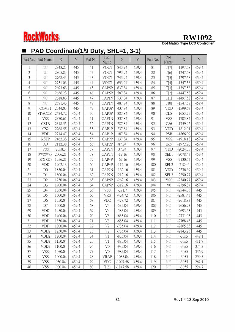
Rev1.4-13 Sep 2010 31
Dot Matrix Type LCD Controller RW1092
PAD Coordinate(1/9 Duty, SHL=1, 3-1) Pad No. Pad Name X Y Pad No.
Pad
Name X Y Pad No.
Pad
Name X Y
1 NC 2843.23 445 41 VOUT 843.94 459.4 81 T[7] -1197.58 459.4
2 NC 2805.83 445 42 VOUT 793.94 459.4 82 T[6] -1247.58 459.4
3 NC 2768.43 445 43 VOUT 743.94 459.4 83 T[5] -1297.58 459.4
4 NC 2731.03 445 44 VOUT 693.94 459.4 84 T[4] -1347.58 459.4
5 NC 2693.63 445 45 CAP5P 637.84 459.4 85 T[3] -1397.58 459.4
6 NC 2656.23 445 46 CAP5P 587.84 459.4 86 T[2] -1447.58 459.4
7 NC 2618.83 445 47 CAP1N 537.84 459.4 87 T[1] -1497.58 459.4
8 NC 2581.43 445 48 CAP1N 487.84 459.4 88 T[0] -1547.58 459.4
9 COMS1 2544.03 445 49 CAP3P 437.84 459.4 89 VDD -1599.67 459.4
10 STACOM 2424.72 459.4 50 CAP3P 387.84 459.4 90 CLS -1653.75 459.4
11 VSS 2370.61 459.4 51 CAP1N 337.84 459.4 91 VSS -1705.84 459.4
12 CS1B 2318.55 459.4 52 CAP1N 287.84 459.4 92 C86 -1759.92 459.4
13 CS2 2268.55 459.4 53 CAP1P 237.84 459.4 93 VDD -1812.01 459.4
14 VDD 2214.47 459.4 54 CAP1P 187.84 459.4 94 PSB -1866.09 459.4
15 RSTP 2162.38 459.4 55 CAP2P 137.84 459.4 95 VSS -1918.18 459.4
16 A0 2112.38 459.4 56 CAP2P 87.84 459.4 96 IRS -1972.26 459.4
17 VSS 2058.3 459.4 57 CAP2N 37.84 459.4 97 VDD -2024.35 459.4
18 RW(XWR) 2006.21 459.4 58 CAP2N -12.16 459.4 98 SEL1 -2078.43 459.4
19 E(XRD) 1956.21 459.4 59 CAP4P -62.16 459.4 99 VSS -2130.52 459.4
20 VDD 1902.13 459.4 60 CAP4P -112.16 459.4 100 SEL2 -2184.6 459.4
21 D0 1850.04 459.4 61 CAP2N -162.16 459.4 101 VDD -2236.69 459.4
22 D1 1800.04 459.4 62 CAP2N -212.16 459.4 102 SEL3 -2290.77 459.4
23 D2 1750.04 459.4 63 CAP6P -262.16 459.4 103 VSS -2340.77 459.4
24 D3 1700.04 459.4 64 CAP6P -312.16 459.4 104 V0 -2396.87 459.4
25 D4 1650.04 459.4 65 VSS -371.7 459.4 105 NC -2544.03 445
26 D5 1600.04 459.4 66 VRS -424.72 459.4 106 NC -2581.43 445
27 D6 1550.04 459.4 67 VDD -477.72 459.4 107 NC -2618.83 445
28 D7 1500.04 459.4 68 V4 -535.04 459.4 108 NC -2656.23 445
29 VDD 1450.04 459.4 69 V4 -585.04 459.4 109 NC -2693.63 445
30 VDD 1400.04 459.4 70 V3 -635.04 459.4 110 NC -2731.03 445
31 VDD 1350.04 459.4 71 V3 -685.04 459.4 111 NC -2768.43 445
32 VDD 1300.04 459.4 72 V2 -735.04 459.4 112 NC -2805.83 445
33 VDD2 1250.04 459.4 73 V2 -785.04 459.4 113 NC -2843.23 445
34 VDD2 1200.04 459.4 74 V1 -835.04 459.4 114 NC -3055 449.1
35 VDD2 1150.04 459.4 75 V1 -885.04 459.4 115 NC -3055 411.7
36 VDD2 1100.04 459.4 76 V0 -935.04 459.4 116 NC -3055 374.3
37 VSS 1050.04 459.4 77 V0 -985.04 459.4 117 NC -3055 336.9
38 VSS 1000.04 459.4 78 VRAB -1035.04 459.4 118 NC -3055 299.5
39 VSS 950.04 459.4 79 VDD -1097.58 459.4 119 NC -3055 262.1
40 VSS 900.04 459.4 80 T[8] -1147.58 459.4 120 NC -3055 224.7

Rev1.4-13 Sep 2010 32
Dot Matrix Type LCD Controller RW1092
PAD Coordinate(1/9 Duty, SHL=1, 3-2) Pad No.
Pad
Name X Y Pad No.
Pad
Name X Y Pad No. Pad Name X Y
121 NC -3055 187.3 161 SEG[23] -2175.3 -423.5 201 SEG[63] -975.3 -423.5
122 NC -3055 149.9 162 SEG[24] -2145.3 -423.5 202 SEG[64] -945.3 -423.5
123 NC -3055 112.5 163 SEG[25] -2115.3 -423.5 203 SEG[65] -915.3 -423.5
124 NC -3055 75.1 164 SEG[26] -2085.3 -423.5 204 SEG[66] -885.3 -423.5
125 NC -3055 37.7 165 SEG[27] -2055.3 -423.5 205 SEG[67] -855.3 -423.5
126 NC -3055 0.3 166 SEG[28] -2025.3 -423.5 206 SEG[68] -825.3 -423.5
127 NC -3055 -37.1 167 SEG[29] -1995.3 -423.5 207 SEG[69] -795.3 -423.5
128 NC -3055 -74.5 168 SEG[30] -1965.3 -423.5 208 SEG[70] -765.3 -423.5
129 COM[0] -3055 -111.9 169 SEG[31] -1935.3 -423.5 209 SEG[71] -735.3 -423.5
130 COM[1] -3055 -149.3 170 SEG[32] -1905.3 -423.5 210 SEG[72] -705.3 -423.5
131 COM[2] -3055 -186.7 171 SEG[33] -1875.3 -423.5 211 SEG[73] -675.3 -423.5
132 COM[3] -3055 -224.1 172 SEG[34] -1845.3 -423.5 212 SEG[74] -645.3 -423.5
133 COM[4] -3055 -261.5 173 SEG[35] -1815.3 -423.5 213 SEG[75] -615.3 -423.5
134 COM[5] -3055 -298.9 174 SEG[36] -1785.3 -423.5 214 SEG[76] -585.3 -423.5
135 COM[6] -3055 -336.3 175 SEG[37] -1755.3 -423.5 215 SEG[77] -555.3 -423.5
136 COM[7] -3055 -373.7 176 SEG[38] -1725.3 -423.5 216 SEG[78] -525.3 -423.5
137 COMS2 -3055 -411.1 177 SEG[39] -1695.3 -423.5 217 SEG[79] -495.3 -423.5
138 SEG[0] -3055 -448.5 178 SEG[40] -1665.3 -423.5 218 SEG[80] -465.3 -423.5
139 SEG[1] -2835.3 -423.5 179 SEG[41] -1635.3 -423.5 219 SEG[81] -435.3 -423.5
140 SEG[2] -2805.3 -423.5 180 SEG[42] -1605.3 -423.5 220 SEG[82] -405.3 -423.5
141 SEG[3] -2775.3 -423.5 181 SEG[43] -1575.3 -423.5 221 SEG[83] -375.3 -423.5
142 SEG[4] -2745.3 -423.5 182 SEG[44] -1545.3 -423.5 222 SEG[84] -345.3 -423.5
143 SEG[5] -2715.3 -423.5 183 SEG[45] -1515.3 -423.5 223 SEG[85] -315.3 -423.5
144 SEG[6] -2685.3 -423.5 184 SEG[46] -1485.3 -423.5 224 SEG[86] -285.3 -423.5
145 SEG[7] -2655.3 -423.5 185 SEG[47] -1455.3 -423.5 225 SEG[87] -255.3 -423.5
146 SEG[8] -2625.3 -423.5 186 SEG[48] -1425.3 -423.5 226 SEG[88] -225.3 -423.5
147 SEG[9] -2595.3 -423.5 187 SEG[49] -1395.3 -423.5 227 SEG[89] -195.3 -423.5
148 SEG[10] -2565.3 -423.5 188 SEG[50] -1365.3 -423.5 228 SEG[90] -165.3 -423.5
149 SEG[11] -2535.3 -423.5 189 SEG[51] -1335.3 -423.5 229 SEG[91] -135.3 -423.5
150 SEG[12] -2505.3 -423.5 190 SEG[52] -1305.3 -423.5 230 SEG[92] -105.3 -423.5
151 SEG[13] -2475.3 -423.5 191 SEG[53] -1275.3 -423.5 231 SEG[93] -75.3 -423.5
152 SEG[14] -2445.3 -423.5 192 SEG[54] -1245.3 -423.5 232 SEG[94] -45.3 -423.5
153 SEG[15] -2415.3 -423.5 193 SEG[55] -1215.3 -423.5 233 SEG[95] -15.3 -423.5
154 SEG[16] -2385.3 -423.5 194 SEG[56] -1185.3 -423.5 234 SEG[96] 14.7 -423.5
155 SEG[17] -2355.3 -423.5 195 SEG[57] -1155.3 -423.5 235 SEG[97] 44.7 -423.5
156 SEG[18] -2325.3 -423.5 196 SEG[58] -1125.3 -423.5 236 SEG[98] 74.7 -423.5
157 SEG[19] -2295.3 -423.5 197 SEG[59] -1095.3 -423.5 237 SEG[99] 104.7 -423.5
158 SEG[20] -2265.3 -423.5 198 SEG[60] -1065.3 -423.5 238 SEG[100] 134.7 -423.5
159 SEG[21] -2235.3 -423.5 199 SEG[61] -1035.3 -423.5 239 SEG[101] 164.7 -423.5
160 SEG[22] -2205.3 -423.5 200 SEG[62] -1005.3 -423.5 240 SEG[102] 194.7 -423.5

Rev1.4-13 Sep 2010 33
Dot Matrix Type LCD Controller RW1092
PAD Coordinate(1/9 Duty, SHL=1, 3-3) Pad No. Pad Name X Y Pad No. Pad Name X Y Pad No.
Pad
Name X Y
241 SEG[103] 224.7 -423.5 281 SEG[143] 1424.7 -423.5 321 SEG[183] 2624.7 -423.5
242 SEG[104] 254.7 -423.5 282 SEG[144] 1454.7 -423.5 322 SEG[184] 2654.7 -423.5
243 SEG[105] 284.7 -423.5 283 SEG[145] 1484.7 -423.5 323 SEG[185] 2684.7 -423.5
244 SEG[106] 314.7 -423.5 284 SEG[146] 1514.7 -423.5 324 SEG[186] 2714.7 -423.5
245 SEG[107] 344.7 -423.5 285 SEG[147] 1544.7 -423.5 325 SEG[187] 2744.7 -423.5
246 SEG[108] 374.7 -423.5 286 SEG[148] 1574.7 -423.5 326 SEG[188] 2774.7 -423.5
247 SEG[109] 404.7 -423.5 287 SEG[149] 1604.7 -423.5 327 SEG[189] 2804.7 -423.5
248 SEG[110] 434.7 -423.5 288 SEG[150] 1634.7 -423.5 328 SEG[190] 2834.7 -423.5
249 SEG[111] 464.7 -423.5 289 SEG[151] 1664.7 -423.5 329 SEG[191] 3055 -448.5
250 SEG[112] 494.7 -423.5 290 SEG[152] 1694.7 -423.5 330 COM[7] 3055 -411.1
251 SEG[113] 524.7 -423.5 291 SEG[153] 1724.7 -423.5 331 COM[6] 3055 -373.7
252 SEG[114] 554.7 -423.5 292 SEG[154] 1754.7 -423.5 332 COM[5] 3055 -336.3
253 SEG[115] 584.7 -423.5 293 SEG[155] 1784.7 -423.5 333 COM[4] 3055 -298.9
254 SEG[116] 614.7 -423.5 294 SEG[156] 1814.7 -423.5 334 COM[3] 3055 -261.5
255 SEG[117] 644.7 -423.5 295 SEG[157] 1844.7 -423.5 335 COM[2] 3055 -224.1
256 SEG[118] 674.7 -423.5 296 SEG[158] 1874.7 -423.5 336 COM[1] 3055 -186.7
257 SEG[119] 704.7 -423.5 297 SEG[159] 1904.7 -423.5 337 COM[0] 3055 -149.3
258 SEG[120] 734.7 -423.5 298 SEG[160] 1934.7 -423.5 338 NC 3055 -111.9
259 SEG[121] 764.7 -423.5 299 SEG[161] 1964.7 -423.5 339 NC 3055 -74.5
260 SEG[122] 794.7 -423.5 300 SEG[162] 1994.7 -423.5 340 NC 3055 -37.1
261 SEG[123] 824.7 -423.5 301 SEG[163] 2024.7 -423.5 341 NC 3055 0.3
262 SEG[124] 854.7 -423.5 302 SEG[164] 2054.7 -423.5 342 NC 3055 37.7
263 SEG[125] 884.7 -423.5 303 SEG[165] 2084.7 -423.5 343 NC 3055 75.1
264 SEG[126] 914.7 -423.5 304 SEG[166] 2114.7 -423.5 344 NC 3055 112.5
265 SEG[127] 944.7 -423.5 305 SEG[167] 2144.7 -423.5 345 NC 3055 149.9
266 SEG[128] 974.7 -423.5 306 SEG[168] 2174.7 -423.5 346 NC 3055 187.3
267 SEG[129] 1004.7 -423.5 307 SEG[169] 2204.7 -423.5 347 NC 3055 224.7
268 SEG[130] 1034.7 -423.5 308 SEG[170] 2234.7 -423.5 348 NC 3055 262.1
269 SEG[131] 1064.7 -423.5 309 SEG[171] 2264.7 -423.5 349 NC 3055 299.5
270 SEG[132] 1094.7 -423.5 310 SEG[172] 2294.7 -423.5 350 NC 3055 336.9
271 SEG[133] 1124.7 -423.5 311 SEG[173] 2324.7 -423.5 351 NC 3055 374.3
272 SEG[134] 1154.7 -423.5 312 SEG[174] 2354.7 -423.5 352 NC 3055 411.7
273 SEG[135] 1184.7 -423.5 313 SEG[175] 2384.7 -423.5 353 NC 3055 449.1
274 SEG[136] 1214.7 -423.5 314 SEG[176] 2414.7 -423.5
275 SEG[137] 1244.7 -423.5 315 SEG[177] 2444.7 -423.5
276 SEG[138] 1274.7 -423.5 316 SEG[178] 2474.7 -423.5
277 SEG[139] 1304.7 -423.5 317 SEG[179] 2504.7 -423.5
278 SEG[140] 1334.7 -423.5 318 SEG[180] 2534.7 -423.5
279 SEG[141] 1364.7 -423.5 319 SEG[181] 2564.7 -423.5
280 SEG[142] 1394.7 -423.5 320 SEG[182] 2594.7 -423.5

Rev1.4-13 Sep 2010 34
Dot Matrix Type LCD Controller RW1092
PAD Coordinate(1/5 Duty, SHL=0, 3-1) Pad No. Pad Name X Y Pad No.
Pad
Name X Y Pad No.
Pad
Name X Y
1 NC 2843.23 445 41 VOUT 843.94 459.4 81 T[7] -1197.58 459.4
2 NC 2805.83 445 42 VOUT 793.94 459.4 82 T[6] -1247.58 459.4
3 NC 2768.43 445 43 VOUT 743.94 459.4 83 T[5] -1297.58 459.4
4 NC 2731.03 445 44 VOUT 693.94 459.4 84 T[4] -1347.58 459.4
5 NC 2693.63 445 45 CAP5P 637.84 459.4 85 T[3] -1397.58 459.4
6 NC 2656.23 445 46 CAP5P 587.84 459.4 86 T[2] -1447.58 459.4
7 NC 2618.83 445 47 CAP1N 537.84 459.4 87 T[1] -1497.58 459.4
8 NC 2581.43 445 48 CAP1N 487.84 459.4 88 T[0] -1547.58 459.4
9 COMS1 2544.03 445 49 CAP3P 437.84 459.4 89 VDD -1599.67 459.4
10 STACOM 2424.72 459.4 50 CAP3P 387.84 459.4 90 CLS -1653.75 459.4
11 VSS 2370.61 459.4 51 CAP1N 337.84 459.4 91 VSS -1705.84 459.4
12 CS1B 2318.55 459.4 52 CAP1N 287.84 459.4 92 C86 -1759.92 459.4
13 CS2 2268.55 459.4 53 CAP1P 237.84 459.4 93 VDD -1812.01 459.4
14 VDD 2214.47 459.4 54 CAP1P 187.84 459.4 94 PSB -1866.09 459.4
15 RSTP 2162.38 459.4 55 CAP2P 137.84 459.4 95 VSS -1918.18 459.4
16 A0 2112.38 459.4 56 CAP2P 87.84 459.4 96 IRS -1972.26 459.4
17 VSS 2058.3 459.4 57 CAP2N 37.84 459.4 97 VDD -2024.35 459.4
18 RW(XWR) 2006.21 459.4 58 CAP2N -12.16 459.4 98 SEL1 -2078.43 459.4
19 E(XRD) 1956.21 459.4 59 CAP4P -62.16 459.4 99 VSS -2130.52 459.4
20 VDD 1902.13 459.4 60 CAP4P -112.16 459.4 100 SEL2 -2184.6 459.4
21 D0 1850.04 459.4 61 CAP2N -162.16 459.4 101 VDD -2236.69 459.4
22 D1 1800.04 459.4 62 CAP2N -212.16 459.4 102 SEL3 -2290.77 459.4
23 D2 1750.04 459.4 63 CAP6P -262.16 459.4 103 VSS -2340.77 459.4
24 D3 1700.04 459.4 64 CAP6P -312.16 459.4 104 V0 -2396.87 459.4
25 D4 1650.04 459.4 65 VSS -371.7 459.4 105 NC -2544.03 445
26 D5 1600.04 459.4 66 VRS -424.72 459.4 106 NC -2581.43 445
27 D6 1550.04 459.4 67 VDD -477.72 459.4 107 NC -2618.83 445
28 D7 1500.04 459.4 68 V4 -535.04 459.4 108 NC -2656.23 445
29 VDD 1450.04 459.4 69 V4 -585.04 459.4 109 NC -2693.63 445
30 VDD 1400.04 459.4 70 V3 -635.04 459.4 110 NC -2731.03 445
31 VDD 1350.04 459.4 71 V3 -685.04 459.4 111 NC -2768.43 445
32 VDD 1300.04 459.4 72 V2 -735.04 459.4 112 NC -2805.83 445
33 VDD2 1250.04 459.4 73 V2 -785.04 459.4 113 NC -2843.23 445
34 VDD2 1200.04 459.4 74 V1 -835.04 459.4 114 NC -3055 449.1
35 VDD2 1150.04 459.4 75 V1 -885.04 459.4 115 NC -3055 411.7
36 VDD2 1100.04 459.4 76 V0 -935.04 459.4 116 NC -3055 374.3
37 VSS 1050.04 459.4 77 V0 -985.04 459.4 117 NC -3055 336.9
38 VSS 1000.04 459.4 78 VRAB -1035.04 459.4 118 NC -3055 299.5
39 VSS 950.04 459.4 79 VDD -1097.58 459.4 119 NC -3055 262.1
40 VSS 900.04 459.4 80 T[8] -1147.58 459.4 120 NC -3055 224.7

Rev1.4-13 Sep 2010 35
Dot Matrix Type LCD Controller RW1092
PAD Coordinate(1/5 Duty, SHL=0, 3-2) Pad No. Pad Name X Y Pad No.
Pad
Name X Y Pad No. Pad Name X Y
121 NC -3055 187.3 161 SEG[23] -2175.3 -423.5 201 SEG[63] -975.3 -423.5
122 NC -3055 149.9 162 SEG[24] -2145.3 -423.5 202 SEG[64] -945.3 -423.5
123 NC -3055 112.5 163 SEG[25] -2115.3 -423.5 203 SEG[65] -915.3 -423.5
124 NC -3055 75.1 164 SEG[26] -2085.3 -423.5 204 SEG[66] -885.3 -423.5
125 NC -3055 37.7 165 SEG[27] -2055.3 -423.5 205 SEG[67] -855.3 -423.5
126 NC -3055 0.3 166 SEG[28] -2025.3 -423.5 206 SEG[68] -825.3 -423.5
127 NC -3055 -37.1 167 SEG[29] -1995.3 -423.5 207 SEG[69] -795.3 -423.5
128 NC -3055 -74.5 168 SEG[30] -1965.3 -423.5 208 SEG[70] -765.3 -423.5
129 NC -3055 -111.9 169 SEG[31] -1935.3 -423.5 209 SEG[71] -735.3 -423.5
130 NC -3055 -149.3 170 SEG[32] -1905.3 -423.5 210 SEG[72] -705.3 -423.5
131 NC -3055 -186.7 171 SEG[33] -1875.3 -423.5 211 SEG[73] -675.3 -423.5
132 NC -3055 -224.1 172 SEG[34] -1845.3 -423.5 212 SEG[74] -645.3 -423.5
133 COM[3] -3055 -261.5 173 SEG[35] -1815.3 -423.5 213 SEG[75] -615.3 -423.5
134 COM[2] -3055 -298.9 174 SEG[36] -1785.3 -423.5 214 SEG[76] -585.3 -423.5
135 COM[1] -3055 -336.3 175 SEG[37] -1755.3 -423.5 215 SEG[77] -555.3 -423.5
136 COM[0] -3055 -373.7 176 SEG[38] -1725.3 -423.5 216 SEG[78] -525.3 -423.5
137 COMS2 -3055 -411.1 177 SEG[39] -1695.3 -423.5 217 SEG[79] -495.3 -423.5
138 SEG[0] -3055 -448.5 178 SEG[40] -1665.3 -423.5 218 SEG[80] -465.3 -423.5
139 SEG[1] -2835.3 -423.5 179 SEG[41] -1635.3 -423.5 219 SEG[81] -435.3 -423.5
140 SEG[2] -2805.3 -423.5 180 SEG[42] -1605.3 -423.5 220 SEG[82] -405.3 -423.5
141 SEG[3] -2775.3 -423.5 181 SEG[43] -1575.3 -423.5 221 SEG[83] -375.3 -423.5
142 SEG[4] -2745.3 -423.5 182 SEG[44] -1545.3 -423.5 222 SEG[84] -345.3 -423.5
143 SEG[5] -2715.3 -423.5 183 SEG[45] -1515.3 -423.5 223 SEG[85] -315.3 -423.5
144 SEG[6] -2685.3 -423.5 184 SEG[46] -1485.3 -423.5 224 SEG[86] -285.3 -423.5
145 SEG[7] -2655.3 -423.5 185 SEG[47] -1455.3 -423.5 225 SEG[87] -255.3 -423.5
146 SEG[8] -2625.3 -423.5 186 SEG[48] -1425.3 -423.5 226 SEG[88] -225.3 -423.5
147 SEG[9] -2595.3 -423.5 187 SEG[49] -1395.3 -423.5 227 SEG[89] -195.3 -423.5
148 SEG[10] -2565.3 -423.5 188 SEG[50] -1365.3 -423.5 228 SEG[90] -165.3 -423.5
149 SEG[11] -2535.3 -423.5 189 SEG[51] -1335.3 -423.5 229 SEG[91] -135.3 -423.5
150 SEG[12] -2505.3 -423.5 190 SEG[52] -1305.3 -423.5 230 SEG[92] -105.3 -423.5
151 SEG[13] -2475.3 -423.5 191 SEG[53] -1275.3 -423.5 231 SEG[93] -75.3 -423.5
152 SEG[14] -2445.3 -423.5 192 SEG[54] -1245.3 -423.5 232 SEG[94] -45.3 -423.5
153 SEG[15] -2415.3 -423.5 193 SEG[55] -1215.3 -423.5 233 SEG[95] -15.3 -423.5
154 SEG[16] -2385.3 -423.5 194 SEG[56] -1185.3 -423.5 234 SEG[96] 14.7 -423.5
155 SEG[17] -2355.3 -423.5 195 SEG[57] -1155.3 -423.5 235 SEG[97] 44.7 -423.5
156 SEG[18] -2325.3 -423.5 196 SEG[58] -1125.3 -423.5 236 SEG[98] 74.7 -423.5
157 SEG[19] -2295.3 -423.5 197 SEG[59] -1095.3 -423.5 237 SEG[99] 104.7 -423.5
158 SEG[20] -2265.3 -423.5 198 SEG[60] -1065.3 -423.5 238 SEG[100] 134.7 -423.5
159 SEG[21] -2235.3 -423.5 199 SEG[61] -1035.3 -423.5 239 SEG[101] 164.7 -423.5
160 SEG[22] -2205.3 -423.5 200 SEG[62] -1005.3 -423.5 240 SEG[102] 194.7 -423.5

Rev1.4-13 Sep 2010 36
Dot Matrix Type LCD Controller RW1092
PAD Coordinate(1/5 Duty, SHL=0, 3-3) Pad No. Pad Name X Y Pad No. Pad Name X Y Pad No.
Pad
Name X Y
241 SEG[103] 224.7 -423.5 281 SEG[143] 1424.7 -423.5 321 SEG[183] 2624.7 -423.5
242 SEG[104] 254.7 -423.5 282 SEG[144] 1454.7 -423.5 322 SEG[184] 2654.7 -423.5
243 SEG[105] 284.7 -423.5 283 SEG[145] 1484.7 -423.5 323 SEG[185] 2684.7 -423.5
244 SEG[106] 314.7 -423.5 284 SEG[146] 1514.7 -423.5 324 SEG[186] 2714.7 -423.5
245 SEG[107] 344.7 -423.5 285 SEG[147] 1544.7 -423.5 325 SEG[187] 2744.7 -423.5
246 SEG[108] 374.7 -423.5 286 SEG[148] 1574.7 -423.5 326 SEG[188] 2774.7 -423.5
247 SEG[109] 404.7 -423.5 287 SEG[149] 1604.7 -423.5 327 SEG[189] 2804.7 -423.5
248 SEG[110] 434.7 -423.5 288 SEG[150] 1634.7 -423.5 328 SEG[190] 2834.7 -423.5
249 SEG[111] 464.7 -423.5 289 SEG[151] 1664.7 -423.5 329 SEG[191] 3055 -448.5
250 SEG[112] 494.7 -423.5 290 SEG[152] 1694.7 -423.5 330 COM[0] 3055 -411.1
251 SEG[113] 524.7 -423.5 291 SEG[153] 1724.7 -423.5 331 COM[1] 3055 -373.7
252 SEG[114] 554.7 -423.5 292 SEG[154] 1754.7 -423.5 332 COM[2] 3055 -336.3
253 SEG[115] 584.7 -423.5 293 SEG[155] 1784.7 -423.5 333 COM[3] 3055 -298.9
254 SEG[116] 614.7 -423.5 294 SEG[156] 1814.7 -423.5 334 NC 3055 -261.5
255 SEG[117] 644.7 -423.5 295 SEG[157] 1844.7 -423.5 335 NC 3055 -224.1
256 SEG[118] 674.7 -423.5 296 SEG[158] 1874.7 -423.5 336 NC 3055 -186.7
257 SEG[119] 704.7 -423.5 297 SEG[159] 1904.7 -423.5 337 NC 3055 -149.3
258 SEG[120] 734.7 -423.5 298 SEG[160] 1934.7 -423.5 338 NC 3055 -111.9
259 SEG[121] 764.7 -423.5 299 SEG[161] 1964.7 -423.5 339 NC 3055 -74.5
260 SEG[122] 794.7 -423.5 300 SEG[162] 1994.7 -423.5 340 NC 3055 -37.1
261 SEG[123] 824.7 -423.5 301 SEG[163] 2024.7 -423.5 341 NC 3055 0.3
262 SEG[124] 854.7 -423.5 302 SEG[164] 2054.7 -423.5 342 NC 3055 37.7
263 SEG[125] 884.7 -423.5 303 SEG[165] 2084.7 -423.5 343 NC 3055 75.1
264 SEG[126] 914.7 -423.5 304 SEG[166] 2114.7 -423.5 344 NC 3055 112.5
265 SEG[127] 944.7 -423.5 305 SEG[167] 2144.7 -423.5 345 NC 3055 149.9
266 SEG[128] 974.7 -423.5 306 SEG[168] 2174.7 -423.5 346 NC 3055 187.3
267 SEG[129] 1004.7 -423.5 307 SEG[169] 2204.7 -423.5 347 NC 3055 224.7
268 SEG[130] 1034.7 -423.5 308 SEG[170] 2234.7 -423.5 348 NC 3055 262.1
269 SEG[131] 1064.7 -423.5 309 SEG[171] 2264.7 -423.5 349 NC 3055 299.5
270 SEG[132] 1094.7 -423.5 310 SEG[172] 2294.7 -423.5 350 NC 3055 336.9
271 SEG[133] 1124.7 -423.5 311 SEG[173] 2324.7 -423.5 351 NC 3055 374.3
272 SEG[134] 1154.7 -423.5 312 SEG[174] 2354.7 -423.5 352 NC 3055 411.7
273 SEG[135] 1184.7 -423.5 313 SEG[175] 2384.7 -423.5 353 NC 3055 449.1
274 SEG[136] 1214.7 -423.5 314 SEG[176] 2414.7 -423.5
275 SEG[137] 1244.7 -423.5 315 SEG[177] 2444.7 -423.5
276 SEG[138] 1274.7 -423.5 316 SEG[178] 2474.7 -423.5
277 SEG[139] 1304.7 -423.5 317 SEG[179] 2504.7 -423.5
278 SEG[140] 1334.7 -423.5 318 SEG[180] 2534.7 -423.5
279 SEG[141] 1364.7 -423.5 319 SEG[181] 2564.7 -423.5
280 SEG[142] 1394.7 -423.5 320 SEG[182] 2594.7 -423.5

Rev1.4-13 Sep 2010 37
Dot Matrix Type LCD Controller RW1092
PAD Coordinate(1/5 Duty, SHL=1, 3-1) Pad No. Pad Name X Y Pad No.
Pad
Name X Y Pad No.
Pad
Name X Y
1 NC 2843.23 445 41 VOUT 843.94 459.4 81 T[7] -1197.58 459.4
2 NC 2805.83 445 42 VOUT 793.94 459.4 82 T[6] -1247.58 459.4
3 NC 2768.43 445 43 VOUT 743.94 459.4 83 T[5] -1297.58 459.4
4 NC 2731.03 445 44 VOUT 693.94 459.4 84 T[4] -1347.58 459.4
5 NC 2693.63 445 45 CAP5P 637.84 459.4 85 T[3] -1397.58 459.4
6 NC 2656.23 445 46 CAP5P 587.84 459.4 86 T[2] -1447.58 459.4
7 NC 2618.83 445 47 CAP1N 537.84 459.4 87 T[1] -1497.58 459.4
8 NC 2581.43 445 48 CAP1N 487.84 459.4 88 T[0] -1547.58 459.4
9 COMS1 2544.03 445 49 CAP3P 437.84 459.4 89 VDD -1599.67 459.4
10 STACOM 2424.72 459.4 50 CAP3P 387.84 459.4 90 CLS -1653.75 459.4
11 VSS 2370.61 459.4 51 CAP1N 337.84 459.4 91 VSS -1705.84 459.4
12 CS1B 2318.55 459.4 52 CAP1N 287.84 459.4 92 C86 -1759.92 459.4
13 CS2 2268.55 459.4 53 CAP1P 237.84 459.4 93 VDD -1812.01 459.4
14 VDD 2214.47 459.4 54 CAP1P 187.84 459.4 94 PSB -1866.09 459.4
15 RSTP 2162.38 459.4 55 CAP2P 137.84 459.4 95 VSS -1918.18 459.4
16 A0 2112.38 459.4 56 CAP2P 87.84 459.4 96 IRS -1972.26 459.4
17 VSS 2058.3 459.4 57 CAP2N 37.84 459.4 97 VDD -2024.35 459.4
18 RW(XWR) 2006.21 459.4 58 CAP2N -12.16 459.4 98 SEL1 -2078.43 459.4
19 E(XRD) 1956.21 459.4 59 CAP4P -62.16 459.4 99 VSS -2130.52 459.4
20 VDD 1902.13 459.4 60 CAP4P -112.16 459.4 100 SEL2 -2184.6 459.4
21 D0 1850.04 459.4 61 CAP2N -162.16 459.4 101 VDD -2236.69 459.4
22 D1 1800.04 459.4 62 CAP2N -212.16 459.4 102 SEL3 -2290.77 459.4
23 D2 1750.04 459.4 63 CAP6P -262.16 459.4 103 VSS -2340.77 459.4
24 D3 1700.04 459.4 64 CAP6P -312.16 459.4 104 V0 -2396.87 459.4
25 D4 1650.04 459.4 65 VSS -371.7 459.4 105 NC -2544.03 445
26 D5 1600.04 459.4 66 VRS -424.72 459.4 106 NC -2581.43 445
27 D6 1550.04 459.4 67 VDD -477.72 459.4 107 NC -2618.83 445
28 D7 1500.04 459.4 68 V4 -535.04 459.4 108 NC -2656.23 445
29 VDD 1450.04 459.4 69 V4 -585.04 459.4 109 NC -2693.63 445
30 VDD 1400.04 459.4 70 V3 -635.04 459.4 110 NC -2731.03 445
31 VDD 1350.04 459.4 71 V3 -685.04 459.4 111 NC -2768.43 445
32 VDD 1300.04 459.4 72 V2 -735.04 459.4 112 NC -2805.83 445
33 VDD2 1250.04 459.4 73 V2 -785.04 459.4 113 NC -2843.23 445
34 VDD2 1200.04 459.4 74 V1 -835.04 459.4 114 NC -3055 449.1
35 VDD2 1150.04 459.4 75 V1 -885.04 459.4 115 NC -3055 411.7
36 VDD2 1100.04 459.4 76 V0 -935.04 459.4 116 NC -3055 374.3
37 VSS 1050.04 459.4 77 V0 -985.04 459.4 117 NC -3055 336.9
38 VSS 1000.04 459.4 78 VRAB -1035.04 459.4 118 NC -3055 299.5
39 VSS 950.04 459.4 79 VDD -1097.58 459.4 119 NC -3055 262.1
40 VSS 900.04 459.4 80 T[8] -1147.58 459.4 120 NC -3055 224.7

Rev1.4-13 Sep 2010 38
Dot Matrix Type LCD Controller RW1092
PAD Coordinate(1/5 Duty, SHL=1, 3-2) Pad No.
Pad
Name X Y Pad No.
Pad
Name X Y Pad No. Pad Name X Y
121 NC -3055 187.3 161 SEG[23] -2175.3 -423.5 201 SEG[63] -975.3 -423.5
122 NC -3055 149.9 162 SEG[24] -2145.3 -423.5 202 SEG[64] -945.3 -423.5
123 NC -3055 112.5 163 SEG[25] -2115.3 -423.5 203 SEG[65] -915.3 -423.5
124 NC -3055 75.1 164 SEG[26] -2085.3 -423.5 204 SEG[66] -885.3 -423.5
125 NC -3055 37.7 165 SEG[27] -2055.3 -423.5 205 SEG[67] -855.3 -423.5
126 NC -3055 0.3 166 SEG[28] -2025.3 -423.5 206 SEG[68] -825.3 -423.5
127 NC -3055 -37.1 167 SEG[29] -1995.3 -423.5 207 SEG[69] -795.3 -423.5
128 NC -3055 -74.5 168 SEG[30] -1965.3 -423.5 208 SEG[70] -765.3 -423.5
129 NC -3055 -111.9 169 SEG[31] -1935.3 -423.5 209 SEG[71] -735.3 -423.5
130 NC -3055 -149.3 170 SEG[32] -1905.3 -423.5 210 SEG[72] -705.3 -423.5
131 NC -3055 -186.7 171 SEG[33] -1875.3 -423.5 211 SEG[73] -675.3 -423.5
132 NC -3055 -224.1 172 SEG[34] -1845.3 -423.5 212 SEG[74] -645.3 -423.5
133 COM[0] -3055 -261.5 173 SEG[35] -1815.3 -423.5 213 SEG[75] -615.3 -423.5
134 COM[1] -3055 -298.9 174 SEG[36] -1785.3 -423.5 214 SEG[76] -585.3 -423.5
135 COM[2] -3055 -336.3 175 SEG[37] -1755.3 -423.5 215 SEG[77] -555.3 -423.5
136 COM[3] -3055 -373.7 176 SEG[38] -1725.3 -423.5 216 SEG[78] -525.3 -423.5
137 COMS2 -3055 -411.1 177 SEG[39] -1695.3 -423.5 217 SEG[79] -495.3 -423.5
138 SEG[0] -3055 -448.5 178 SEG[40] -1665.3 -423.5 218 SEG[80] -465.3 -423.5
139 SEG[1] -2835.3 -423.5 179 SEG[41] -1635.3 -423.5 219 SEG[81] -435.3 -423.5
140 SEG[2] -2805.3 -423.5 180 SEG[42] -1605.3 -423.5 220 SEG[82] -405.3 -423.5
141 SEG[3] -2775.3 -423.5 181 SEG[43] -1575.3 -423.5 221 SEG[83] -375.3 -423.5
142 SEG[4] -2745.3 -423.5 182 SEG[44] -1545.3 -423.5 222 SEG[84] -345.3 -423.5
143 SEG[5] -2715.3 -423.5 183 SEG[45] -1515.3 -423.5 223 SEG[85] -315.3 -423.5
144 SEG[6] -2685.3 -423.5 184 SEG[46] -1485.3 -423.5 224 SEG[86] -285.3 -423.5
145 SEG[7] -2655.3 -423.5 185 SEG[47] -1455.3 -423.5 225 SEG[87] -255.3 -423.5
146 SEG[8] -2625.3 -423.5 186 SEG[48] -1425.3 -423.5 226 SEG[88] -225.3 -423.5
147 SEG[9] -2595.3 -423.5 187 SEG[49] -1395.3 -423.5 227 SEG[89] -195.3 -423.5
148 SEG[10] -2565.3 -423.5 188 SEG[50] -1365.3 -423.5 228 SEG[90] -165.3 -423.5
149 SEG[11] -2535.3 -423.5 189 SEG[51] -1335.3 -423.5 229 SEG[91] -135.3 -423.5
150 SEG[12] -2505.3 -423.5 190 SEG[52] -1305.3 -423.5 230 SEG[92] -105.3 -423.5
151 SEG[13] -2475.3 -423.5 191 SEG[53] -1275.3 -423.5 231 SEG[93] -75.3 -423.5
152 SEG[14] -2445.3 -423.5 192 SEG[54] -1245.3 -423.5 232 SEG[94] -45.3 -423.5
153 SEG[15] -2415.3 -423.5 193 SEG[55] -1215.3 -423.5 233 SEG[95] -15.3 -423.5
154 SEG[16] -2385.3 -423.5 194 SEG[56] -1185.3 -423.5 234 SEG[96] 14.7 -423.5
155 SEG[17] -2355.3 -423.5 195 SEG[57] -1155.3 -423.5 235 SEG[97] 44.7 -423.5
156 SEG[18] -2325.3 -423.5 196 SEG[58] -1125.3 -423.5 236 SEG[98] 74.7 -423.5
157 SEG[19] -2295.3 -423.5 197 SEG[59] -1095.3 -423.5 237 SEG[99] 104.7 -423.5
158 SEG[20] -2265.3 -423.5 198 SEG[60] -1065.3 -423.5 238 SEG[100] 134.7 -423.5
159 SEG[21] -2235.3 -423.5 199 SEG[61] -1035.3 -423.5 239 SEG[101] 164.7 -423.5
160 SEG[22] -2205.3 -423.5 200 SEG[62] -1005.3 -423.5 240 SEG[102] 194.7 -423.5

Rev1.4-13 Sep 2010 39
Dot Matrix Type LCD Controller RW1092
PAD Coordinate(1/5 Duty, SHL=1, 3-3) Pad No. Pad Name X Y Pad No. Pad Name X Y Pad No.
Pad
Name X Y
241 SEG[103] 224.7 -423.5 281 SEG[143] 1424.7 -423.5 321 SEG[183] 2624.7 -423.5
242 SEG[104] 254.7 -423.5 282 SEG[144] 1454.7 -423.5 322 SEG[184] 2654.7 -423.5
243 SEG[105] 284.7 -423.5 283 SEG[145] 1484.7 -423.5 323 SEG[185] 2684.7 -423.5
244 SEG[106] 314.7 -423.5 284 SEG[146] 1514.7 -423.5 324 SEG[186] 2714.7 -423.5
245 SEG[107] 344.7 -423.5 285 SEG[147] 1544.7 -423.5 325 SEG[187] 2744.7 -423.5
246 SEG[108] 374.7 -423.5 286 SEG[148] 1574.7 -423.5 326 SEG[188] 2774.7 -423.5
247 SEG[109] 404.7 -423.5 287 SEG[149] 1604.7 -423.5 327 SEG[189] 2804.7 -423.5
248 SEG[110] 434.7 -423.5 288 SEG[150] 1634.7 -423.5 328 SEG[190] 2834.7 -423.5
249 SEG[111] 464.7 -423.5 289 SEG[151] 1664.7 -423.5 329 SEG[191] 3055 -448.5
250 SEG[112] 494.7 -423.5 290 SEG[152] 1694.7 -423.5 330 COM[3] 3055 -411.1
251 SEG[113] 524.7 -423.5 291 SEG[153] 1724.7 -423.5 331 COM[2] 3055 -373.7
252 SEG[114] 554.7 -423.5 292 SEG[154] 1754.7 -423.5 332 COM[1] 3055 -336.3
253 SEG[115] 584.7 -423.5 293 SEG[155] 1784.7 -423.5 333 COM[0] 3055 -298.9
254 SEG[116] 614.7 -423.5 294 SEG[156] 1814.7 -423.5 334 NC 3055 -261.5
255 SEG[117] 644.7 -423.5 295 SEG[157] 1844.7 -423.5 335 NC 3055 -224.1
256 SEG[118] 674.7 -423.5 296 SEG[158] 1874.7 -423.5 336 NC 3055 -186.7
257 SEG[119] 704.7 -423.5 297 SEG[159] 1904.7 -423.5 337 NC 3055 -149.3
258 SEG[120] 734.7 -423.5 298 SEG[160] 1934.7 -423.5 338 NC 3055 -111.9
259 SEG[121] 764.7 -423.5 299 SEG[161] 1964.7 -423.5 339 NC 3055 -74.5
260 SEG[122] 794.7 -423.5 300 SEG[162] 1994.7 -423.5 340 NC 3055 -37.1
261 SEG[123] 824.7 -423.5 301 SEG[163] 2024.7 -423.5 341 NC 3055 0.3
262 SEG[124] 854.7 -423.5 302 SEG[164] 2054.7 -423.5 342 NC 3055 37.7
263 SEG[125] 884.7 -423.5 303 SEG[165] 2084.7 -423.5 343 NC 3055 75.1
264 SEG[126] 914.7 -423.5 304 SEG[166] 2114.7 -423.5 344 NC 3055 112.5
265 SEG[127] 944.7 -423.5 305 SEG[167] 2144.7 -423.5 345 NC 3055 149.9
266 SEG[128] 974.7 -423.5 306 SEG[168] 2174.7 -423.5 346 NC 3055 187.3
267 SEG[129] 1004.7 -423.5 307 SEG[169] 2204.7 -423.5 347 NC 3055 224.7
268 SEG[130] 1034.7 -423.5 308 SEG[170] 2234.7 -423.5 348 NC 3055 262.1
269 SEG[131] 1064.7 -423.5 309 SEG[171] 2264.7 -423.5 349 NC 3055 299.5
270 SEG[132] 1094.7 -423.5 310 SEG[172] 2294.7 -423.5 350 NC 3055 336.9
271 SEG[133] 1124.7 -423.5 311 SEG[173] 2324.7 -423.5 351 NC 3055 374.3
272 SEG[134] 1154.7 -423.5 312 SEG[174] 2354.7 -423.5 352 NC 3055 411.7
273 SEG[135] 1184.7 -423.5 313 SEG[175] 2384.7 -423.5 353 NC 3055 449.1
274 SEG[136] 1214.7 -423.5 314 SEG[176] 2414.7 -423.5
275 SEG[137] 1244.7 -423.5 315 SEG[177] 2444.7 -423.5
276 SEG[138] 1274.7 -423.5 316 SEG[178] 2474.7 -423.5
277 SEG[139] 1304.7 -423.5 317 SEG[179] 2504.7 -423.5
278 SEG[140] 1334.7 -423.5 318 SEG[180] 2534.7 -423.5
279 SEG[141] 1364.7 -423.5 319 SEG[181] 2564.7 -423.5
280 SEG[142] 1394.7 -423.5 320 SEG[182] 2594.7 -423.5

Rev1.4-13 Sep 2010 40
Dot Matrix Type LCD Controller RW1092
PAD Coordinate( Static , SHL=0, 3-1) Pad No. Pad Name X Y Pad No.
Pad
Name X Y Pad No.
Pad
Name X Y
1 NC 2843.23 445 41 VOUT 843.94 459.4 81 T[7] -1197.58 459.4
2 NC 2805.83 445 42 VOUT 793.94 459.4 82 T[6] -1247.58 459.4
3 NC 2768.43 445 43 VOUT 743.94 459.4 83 T[5] -1297.58 459.4
4 NC 2731.03 445 44 VOUT 693.94 459.4 84 T[4] -1347.58 459.4
5 NC 2693.63 445 45 CAP5P 637.84 459.4 85 T[3] -1397.58 459.4
6 NC 2656.23 445 46 CAP5P 587.84 459.4 86 T[2] -1447.58 459.4
7 NC 2618.83 445 47 CAP1N 537.84 459.4 87 T[1] -1497.58 459.4
8 NC 2581.43 445 48 CAP1N 487.84 459.4 88 T[0] -1547.58 459.4
9 COMS1 2544.03 445 49 CAP3P 437.84 459.4 89 VDD -1599.67 459.4
10 STACOM 2424.72 459.4 50 CAP3P 387.84 459.4 90 CLS -1653.75 459.4
11 VSS 2370.61 459.4 51 CAP1N 337.84 459.4 91 VSS -1705.84 459.4
12 CS1B 2318.55 459.4 52 CAP1N 287.84 459.4 92 C86 -1759.92 459.4
13 CS2 2268.55 459.4 53 CAP1P 237.84 459.4 93 VDD -1812.01 459.4
14 VDD 2214.47 459.4 54 CAP1P 187.84 459.4 94 PSB -1866.09 459.4
15 RSTP 2162.38 459.4 55 CAP2P 137.84 459.4 95 VSS -1918.18 459.4
16 A0 2112.38 459.4 56 CAP2P 87.84 459.4 96 IRS -1972.26 459.4
17 VSS 2058.3 459.4 57 CAP2N 37.84 459.4 97 VDD -2024.35 459.4
18 RW(XWR) 2006.21 459.4 58 CAP2N -12.16 459.4 98 SEL1 -2078.43 459.4
19 E(XRD) 1956.21 459.4 59 CAP4P -62.16 459.4 99 VSS -2130.52 459.4
20 VDD 1902.13 459.4 60 CAP4P -112.16 459.4 100 SEL2 -2184.6 459.4
21 D0 1850.04 459.4 61 CAP2N -162.16 459.4 101 VDD -2236.69 459.4
22 D1 1800.04 459.4 62 CAP2N -212.16 459.4 102 SEL3 -2290.77 459.4
23 D2 1750.04 459.4 63 CAP6P -262.16 459.4 103 VSS -2340.77 459.4
24 D3 1700.04 459.4 64 CAP6P -312.16 459.4 104 V0 -2396.87 459.4
25 D4 1650.04 459.4 65 VSS -371.7 459.4 105 NC -2544.03 445
26 D5 1600.04 459.4 66 VRS -424.72 459.4 106 NC -2581.43 445
27 D6 1550.04 459.4 67 VDD -477.72 459.4 107 NC -2618.83 445
28 D7 1500.04 459.4 68 V4 -535.04 459.4 108 NC -2656.23 445
29 VDD 1450.04 459.4 69 V4 -585.04 459.4 109 NC -2693.63 445
30 VDD 1400.04 459.4 70 V3 -635.04 459.4 110 NC -2731.03 445
31 VDD 1350.04 459.4 71 V3 -685.04 459.4 111 NC -2768.43 445
32 VDD 1300.04 459.4 72 V2 -735.04 459.4 112 NC -2805.83 445
33 VDD2 1250.04 459.4 73 V2 -785.04 459.4 113 NC -2843.23 445
34 VDD2 1200.04 459.4 74 V1 -835.04 459.4 114 NC -3055 449.1
35 VDD2 1150.04 459.4 75 V1 -885.04 459.4 115 NC -3055 411.7
36 VDD2 1100.04 459.4 76 V0 -935.04 459.4 116 NC -3055 374.3
37 VSS 1050.04 459.4 77 V0 -985.04 459.4 117 NC -3055 336.9
38 VSS 1000.04 459.4 78 VRAB -1035.04 459.4 118 NC -3055 299.5
39 VSS 950.04 459.4 79 VDD -1097.58 459.4 119 NC -3055 262.1
40 VSS 900.04 459.4 80 T[8] -1147.58 459.4 120 NC -3055 224.7

Rev1.4-13 Sep 2010 41
Dot Matrix Type LCD Controller RW1092
PAD Coordinate( Static , SHL=0, 3-2) Pad No. Pad Name X Y Pad No.
Pad
Name X Y Pad No. Pad Name X Y
121 NC -3055 187.3 161 SEG[23] -2175.3 -423.5 201 SEG[63] -975.3 -423.5
122 NC -3055 149.9 162 SEG[24] -2145.3 -423.5 202 SEG[64] -945.3 -423.5
123 NC -3055 112.5 163 SEG[25] -2115.3 -423.5 203 SEG[65] -915.3 -423.5
124 NC -3055 75.1 164 SEG[26] -2085.3 -423.5 204 SEG[66] -885.3 -423.5
125 NC -3055 37.7 165 SEG[27] -2055.3 -423.5 205 SEG[67] -855.3 -423.5
126 NC -3055 0.3 166 SEG[28] -2025.3 -423.5 206 SEG[68] -825.3 -423.5
127 NC -3055 -37.1 167 SEG[29] -1995.3 -423.5 207 SEG[69] -795.3 -423.5
128 NC -3055 -74.5 168 SEG[30] -1965.3 -423.5 208 SEG[70] -765.3 -423.5
129 NC -3055 -111.9 169 SEG[31] -1935.3 -423.5 209 SEG[71] -735.3 -423.5
130 NC -3055 -149.3 170 SEG[32] -1905.3 -423.5 210 SEG[72] -705.3 -423.5
131 NC -3055 -186.7 171 SEG[33] -1875.3 -423.5 211 SEG[73] -675.3 -423.5
132 NC -3055 -224.1 172 SEG[34] -1845.3 -423.5 212 SEG[74] -645.3 -423.5
133 NC -3055 -261.5 173 SEG[35] -1815.3 -423.5 213 SEG[75] -615.3 -423.5
134 NC -3055 -298.9 174 SEG[36] -1785.3 -423.5 214 SEG[76] -585.3 -423.5
135 NC -3055 -336.3 175 SEG[37] -1755.3 -423.5 215 SEG[77] -555.3 -423.5
136 NC -3055 -373.7 176 SEG[38] -1725.3 -423.5 216 SEG[78] -525.3 -423.5
137 COMS2 -3055 -411.1 177 SEG[39] -1695.3 -423.5 217 SEG[79] -495.3 -423.5
138 SEG[0] -3055 -448.5 178 SEG[40] -1665.3 -423.5 218 SEG[80] -465.3 -423.5
139 SEG[1] -2835.3 -423.5 179 SEG[41] -1635.3 -423.5 219 SEG[81] -435.3 -423.5
140 SEG[2] -2805.3 -423.5 180 SEG[42] -1605.3 -423.5 220 SEG[82] -405.3 -423.5
141 SEG[3] -2775.3 -423.5 181 SEG[43] -1575.3 -423.5 221 SEG[83] -375.3 -423.5
142 SEG[4] -2745.3 -423.5 182 SEG[44] -1545.3 -423.5 222 SEG[84] -345.3 -423.5
143 SEG[5] -2715.3 -423.5 183 SEG[45] -1515.3 -423.5 223 SEG[85] -315.3 -423.5
144 SEG[6] -2685.3 -423.5 184 SEG[46] -1485.3 -423.5 224 SEG[86] -285.3 -423.5
145 SEG[7] -2655.3 -423.5 185 SEG[47] -1455.3 -423.5 225 SEG[87] -255.3 -423.5
146 SEG[8] -2625.3 -423.5 186 SEG[48] -1425.3 -423.5 226 SEG[88] -225.3 -423.5
147 SEG[9] -2595.3 -423.5 187 SEG[49] -1395.3 -423.5 227 SEG[89] -195.3 -423.5
148 SEG[10] -2565.3 -423.5 188 SEG[50] -1365.3 -423.5 228 SEG[90] -165.3 -423.5
149 SEG[11] -2535.3 -423.5 189 SEG[51] -1335.3 -423.5 229 SEG[91] -135.3 -423.5
150 SEG[12] -2505.3 -423.5 190 SEG[52] -1305.3 -423.5 230 SEG[92] -105.3 -423.5
151 SEG[13] -2475.3 -423.5 191 SEG[53] -1275.3 -423.5 231 SEG[93] -75.3 -423.5
152 SEG[14] -2445.3 -423.5 192 SEG[54] -1245.3 -423.5 232 SEG[94] -45.3 -423.5
153 SEG[15] -2415.3 -423.5 193 SEG[55] -1215.3 -423.5 233 SEG[95] -15.3 -423.5
154 SEG[16] -2385.3 -423.5 194 SEG[56] -1185.3 -423.5 234 SEG[96] 14.7 -423.5
155 SEG[17] -2355.3 -423.5 195 SEG[57] -1155.3 -423.5 235 SEG[97] 44.7 -423.5
156 SEG[18] -2325.3 -423.5 196 SEG[58] -1125.3 -423.5 236 SEG[98] 74.7 -423.5
157 SEG[19] -2295.3 -423.5 197 SEG[59] -1095.3 -423.5 237 SEG[99] 104.7 -423.5
158 SEG[20] -2265.3 -423.5 198 SEG[60] -1065.3 -423.5 238 SEG[100] 134.7 -423.5
159 SEG[21] -2235.3 -423.5 199 SEG[61] -1035.3 -423.5 239 SEG[101] 164.7 -423.5
160 SEG[22] -2205.3 -423.5 200 SEG[62] -1005.3 -423.5 240 SEG[102] 194.7 -423.5

Rev1.4-13 Sep 2010 42
Dot Matrix Type LCD Controller RW1092
PAD Coordinate( Static , SHL=0, 3-3) Pad No. Pad Name X Y Pad No. Pad Name X Y Pad No.
Pad
Name X Y
241 SEG[103] 224.7 -423.5 281 SEG[143] 1424.7 -423.5 321 SEG[183] 2624.7 -423.5
242 SEG[104] 254.7 -423.5 282 SEG[144] 1454.7 -423.5 322 SEG[184] 2654.7 -423.5
243 SEG[105] 284.7 -423.5 283 SEG[145] 1484.7 -423.5 323 SEG[185] 2684.7 -423.5
244 SEG[106] 314.7 -423.5 284 SEG[146] 1514.7 -423.5 324 SEG[186] 2714.7 -423.5
245 SEG[107] 344.7 -423.5 285 SEG[147] 1544.7 -423.5 325 SEG[187] 2744.7 -423.5
246 SEG[108] 374.7 -423.5 286 SEG[148] 1574.7 -423.5 326 SEG[188] 2774.7 -423.5
247 SEG[109] 404.7 -423.5 287 SEG[149] 1604.7 -423.5 327 SEG[189] 2804.7 -423.5
248 SEG[110] 434.7 -423.5 288 SEG[150] 1634.7 -423.5 328 SEG[190] 2834.7 -423.5
249 SEG[111] 464.7 -423.5 289 SEG[151] 1664.7 -423.5 329 SEG[191] 3055 -448.5
250 SEG[112] 494.7 -423.5 290 SEG[152] 1694.7 -423.5 330 NC 3055 -411.1
251 SEG[113] 524.7 -423.5 291 SEG[153] 1724.7 -423.5 331 NC 3055 -373.7
252 SEG[114] 554.7 -423.5 292 SEG[154] 1754.7 -423.5 332 NC 3055 -336.3
253 SEG[115] 584.7 -423.5 293 SEG[155] 1784.7 -423.5 333 NC 3055 -298.9
254 SEG[116] 614.7 -423.5 294 SEG[156] 1814.7 -423.5 334 NC 3055 -261.5
255 SEG[117] 644.7 -423.5 295 SEG[157] 1844.7 -423.5 335 NC 3055 -224.1
256 SEG[118] 674.7 -423.5 296 SEG[158] 1874.7 -423.5 336 NC 3055 -186.7
257 SEG[119] 704.7 -423.5 297 SEG[159] 1904.7 -423.5 337 NC 3055 -149.3
258 SEG[120] 734.7 -423.5 298 SEG[160] 1934.7 -423.5 338 NC 3055 -111.9
259 SEG[121] 764.7 -423.5 299 SEG[161] 1964.7 -423.5 339 NC 3055 -74.5
260 SEG[122] 794.7 -423.5 300 SEG[162] 1994.7 -423.5 340 NC 3055 -37.1
261 SEG[123] 824.7 -423.5 301 SEG[163] 2024.7 -423.5 341 NC 3055 0.3
262 SEG[124] 854.7 -423.5 302 SEG[164] 2054.7 -423.5 342 NC 3055 37.7
263 SEG[125] 884.7 -423.5 303 SEG[165] 2084.7 -423.5 343 NC 3055 75.1
264 SEG[126] 914.7 -423.5 304 SEG[166] 2114.7 -423.5 344 NC 3055 112.5
265 SEG[127] 944.7 -423.5 305 SEG[167] 2144.7 -423.5 345 NC 3055 149.9
266 SEG[128] 974.7 -423.5 306 SEG[168] 2174.7 -423.5 346 NC 3055 187.3
267 SEG[129] 1004.7 -423.5 307 SEG[169] 2204.7 -423.5 347 NC 3055 224.7
268 SEG[130] 1034.7 -423.5 308 SEG[170] 2234.7 -423.5 348 NC 3055 262.1
269 SEG[131] 1064.7 -423.5 309 SEG[171] 2264.7 -423.5 349 NC 3055 299.5
270 SEG[132] 1094.7 -423.5 310 SEG[172] 2294.7 -423.5 350 NC 3055 336.9
271 SEG[133] 1124.7 -423.5 311 SEG[173] 2324.7 -423.5 351 NC 3055 374.3
272 SEG[134] 1154.7 -423.5 312 SEG[174] 2354.7 -423.5 352 NC 3055 411.7
273 SEG[135] 1184.7 -423.5 313 SEG[175] 2384.7 -423.5 353 NC 3055 449.1
274 SEG[136] 1214.7 -423.5 314 SEG[176] 2414.7 -423.5
275 SEG[137] 1244.7 -423.5 315 SEG[177] 2444.7 -423.5
276 SEG[138] 1274.7 -423.5 316 SEG[178] 2474.7 -423.5
277 SEG[139] 1304.7 -423.5 317 SEG[179] 2504.7 -423.5
278 SEG[140] 1334.7 -423.5 318 SEG[180] 2534.7 -423.5
279 SEG[141] 1364.7 -423.5 319 SEG[181] 2564.7 -423.5
280 SEG[142] 1394.7 -423.5 320 SEG[182] 2594.7 -423.5

Rev1.4-13 Sep 2010 43
Dot Matrix Type LCD Controller RW1092
BLOCK DIAGRAM (DUTY=1/97)

Rev1.4-13 Sep 2010 44
Dot Matrix Type LCD Controller RW1092
BLOCK DIAGRAM (DUTY=1/65,1/33,1/17,1/9,1/5) COMMON=64,32,16,8,4 for different duty selection

Rev1.4-13 Sep 2010 45
Dot Matrix Type LCD Controller RW1092
BLOCK DIAGRAM (Static)

Rev1.4-13 Sep 2010 46
Dot Matrix Type LCD Controller RW1092
PIN DESCRIPITON
Power Supply Pin
Pin Name I/O Function No. of Pins
VDD Power Supply Power supply 4
VDD2 Power Supply Power supply for DC-DC Converter 4
VSS Power Supply Ground 4
VRS Power Supply
This is the internal-output VREG power supply for the LCD power supply voltage regulator. 1
V0, V1, V2, V3,
V4
Power Supply
This is a multi-level power supply for the liquid crystal drive. The voltage Supply applied is determined by the liquid crystal cell, and is changed through the use of a resistive voltage divided or through changing the impedance using an op. amp. Voltage levels are determined based on VSS, and must maintain the relative magnitudes shown below.
V0 ≧V1 ≧V2 ≧V3 ≧V4 ≧VSS When the power supply turns ON, the internal power supply circuits produce the V1 to V4 voltages shown below. The voltage settings are selected using the LCD bias set command.
11
LCD Power Supply Pin
Pin Name I/O Function No. of Pins
CAP1P O DC/DC voltage converter. Connect a capacitor between this terminal and the CAP1N terminal. 2
CAP1N O DC/DC voltage converter. Connect a capacitor between this terminal and the CAP1P terminal. 4
CAP2P O DC/DC voltage converter. Connect a capacitor between this terminal and the CAP2N terminal. 2
CAP2N O DC/DC voltage converter. Connect a capacitor between this terminal and the CAP2P terminal. 4
CAP3P O DC/DC voltage converter. Connect a capacitor between this terminal and the CAP1N terminal. 2
CAP4P O DC/DC voltage converter. Connect a capacitor between this terminal and the CAP2N terminal. 2
CAP5P O DC/DC voltage converter. Connect a capacitor between this terminal and the CAP1N terminal. 2
CAP6P O DC/DC voltage converter. Connect a capacitor between this terminal and the CAP2N terminal. 2
VOUT O DC/DC voltage converter. Connect a capacitor between this terminal and VSS or VDD 2
VRAB I
Output voltage regulator terminal. Provides the voltage between VSS and V0 through a resistive voltage divider. IRS = “L” : the V0 voltage regulator internal resistors are not used . IRS = “H” : the V0 voltage regulator internal resistors are used .
1

Rev1.4-13 Sep 2010 47
Dot Matrix Type LCD Controller RW1092
System Bus Connection Pin
Pin Name I/O Function No. of Pins
D0 to D7 I/O
This is an 8-bit bi-directional data bus that connects to an 8-bit standard MPU data bus. ----------------------------------------------------------------------------------------------------- When the 4/3 line serial interface is selected (PSB= “L”,C86=”H”) : D7: serial data input (SI) ; D6 : the serial clock input (SCL). D0 to D5 are set to high impedance. When the chip select is not active, D0 to D7 are set to high impedance. ----------------------------------------------------------------------------------------------------- When the IIC serial interface selected (PSB=”L”, C86=”L”); D7: serial clock input (SCL) D6 , D5 , D4: serial input data (SDA_IN) D3, D2: (SDA_OUT) serial data acknowledge for the IIC interface. By connecting SDA_OUT to SDA_IN externally, the SDA line becomes fully IIC interface compatible. Having the acknowledge output separated from the serial data line is advantageous in chip on glass (COG) applications. In COG application where the track resistance from the SDA_OUT pad to the system SDA line can be significant, a potential divider is generated by the bus pull-up resistor and the ITO track resistance. It is possible during the acknowledge cycle the RW1092 will not be able to create a valid logic 0 level. By splitting the SDA_IN input from the SDA_OUT output the device could be used in a mode that ignores the acknowledge bit. In COG applications where the acknowledge cycle is required, it is necessary to minimize the track resistance from the SDA_OUT pad to the system SDA line to guarantee a valid low level. D6, D5, ….D2 must be connected together (SDA) D1, D0: Is slave address (SA) bit1, 0, must connect to VDD or VSS. When chip select is not active, D0 to D7 is high impedance.
8
A0 I
This is connect to the least significant bit of the normal MPU address bus, and it determines whether the data bits are data or a command. A0 = “H”: Indicates that D0 to D7 are display data. A0 = “L”: Indicates that D0 to D7 are control data.
1
RSTP I When RSTP is set to “L,” the settings are initialized. The reset operation is performed by the RSTP signal level. 1
CS1B CS2 I This is the chip select signal. When CS1B = “L” and CS2 = “H,” then the
chip select becomes active, and data/command I/O is enabled. 2
E(XRD)
I
• When connected to an 8080 MPU, this is active LOW. (E) This pin is connected to the XRD signal of the 8080 MPU, and the RW1092 series data bus is in an output status when this signal is “L”. • When connected to a 6800 Series MPU, this is active HIGH. This is the 6800 Series MPU enable clock input terminal.
1
RW(XWR)
I
• When connected to an 8080 MPU, this is active LOW. RW This terminal connects to the 8080 MPU XWR signal. The signals on the data bus are latched at the rising edge of the XWR signal. • When connected to a 6800 Series MPU: This is the read/write control signal input terminal. When RW = “H”: Read. When RW = “L”: Write.
1

Rev1.4-13 Sep 2010 48
Dot Matrix Type LCD Controller RW1092
Pin Name I/O Function No. of Pins
PSB,C86
Interface selection pins
PSB , C86 Interface
0 , 0 IIC
0 , 1 SPI4/SPI3
1 , 0 8-bit parallel 8080 series MPU
1 , 1 8-bit parallel 6800series MPU
CLS I
Terminal to select whether or enable or disable the display clock internal oscillator circuit. CLS = “H” : used Internal oscillator circuit , STACOM output mode enable CLS = “L” : used external clock input .(internal oscillator is disable) When CLS = “L”, input the display clock through the STACOM terminal.
1
STACOM I/O
This is the Static display Common Output or clock input terminal.( selected by software)
CLS STACOM
“H” “L”
Output Input
1
IRS I
This terminal selects the resistors for the V0 voltage level adjustment. IRS = “H”: Use the internal resistors IRS = “L”: Do not use the internal resistors. The V0 voltage level is regulated by an external resistive voltage divider attached to the VRAB terminal
1
SEL3 SEL2 SEL1
I
These pins are DUTY selection. BE=0 BE=1 SEL 3 , 2 , 1 DUTY
BIAS=(0,1) BIAS=(0,1) 0 , 0 , 0 static 1/2 -
0 , 0 , 0 1/5 1/3, 1/2 -
0 , 0 , 1 1/9 1/5, 1/4 1/3, 1/2
0 , 1 , 0 1/17 1/5, 1/4 1/3, 1/2
0 , 1 , 1 1/33 1/6, 1/4 1/5 , 1/3
1 , 0 , 0 1/65(S1065) 1/9, 1/7 1/8, 1/6
1 , 0 , 1 1/65(S1575) 1/9, 1/7 1/8, 1/6
1 , 1 , 0 1/65 1/9, 1/7 1/8, 1/6
1, 1 , 1 1/97 1/10, 1/8 1/9, 1/7
3
TEST0 ~ 8 I These are terminals for IC testing. They are set to open. 9

Rev1.4-13 Sep 2010 49
Dot Matrix Type LCD Controller RW1092
LCD Driver Pin
Pin Name I/O Function No. of Pins
SEG0 to
SEGn O
These are the LCD segment drive outputs. Through a combination of the contents of the display RAM and with the FR signal, a single level is selected from VSS, V3, V2, and V0. n=191 for Duty 1/65,1/33, 1/17, 1/9, 1/5 n=159 for Duty 1/97
Output Voltage RAM DATA FR
Normal Display Reverse Display
H H V0 V2
H L VSS V3
L H V2 V0
L L V3 VSS
Power save L VSS
192
COM0 to
COMn O
Through a combination of the contents of the scan data and with the FR signal, a single level is selected from VSS, V4, V1, and V0. n=63, 31, 15, 7, 4 for Duty 1/65,1/33, 1/17, 1/9, 1/5 n=95 for Duty 1/97
Scan Data FR Output Voltage
H H VSS
H L V0
L H V1
L L V4
Power save L VSS
67
COMS O
These are the COM output terminals for the indicator. Both terminals output the same signal. Leave these open if they are not used.
2
RW1092 I/O PIN ITO Resister Limitation PIN Name ITO Resister
C86 , PSB ,SEL1,SEL2,SEL3 , CLS ,IRS No Limitation TEST0…8 Floating VDD, VDD2,VSS, VRS, VOUT ,V0, VRAB <100Ω CS1B ,CS2 ,STACOM, E(XRD) , RW(XWR) , A0 , D0 …D7 <1KΩ V1 , V2 , V3 , V4 , CAP1P , CAP1N , CAP2P , CAP2N , CAP3P , CAP4P , CAP5P,CAP6P
<500Ω
RSTP <10KΩ

Rev1.4-13 Sep 2010 50
Dot Matrix Type LCD Controller RW1092
DESCRIPTION OF FUNCTION The MPU Interface Selecting the Interface Type With the RW1092 chips, data transfers are done through an 8-bit parallel data bus (D7 to D0) or through a serial data input (SI). Through selecting the PSB/ C86 terminal polarity to the “H” or “L” it is
possible to select either parallel data input or serial data input as shown in Table 1.
Table 1
Interface PSB C86 CS1B CS2 A0 E(XRD) RW(XWR) D7 D6 D5~D0
6800 H H CS1B CS2 A0 E RW D7 D6 D5~D0
8080 H L CS1B CS2 A0 XRD XWR D7 D6 D5~ D0
4SPI L H CS1B H A0 — — SI SCL (HZ)
3SPI L H CS1B H L — — SI SCL (HZ)
IIC L L — — — — — SCL SDA_IN:D6~D5
SDA_OUT: D3~D2 SA[1:0]: D1~ D0
“—” indicates fixed to either “H” or to “L”
The Parallel Interface When the parallel interface has been selected (PSB=“H”), then it is possible to connect directly to either an 8080-system MPU or a 6800 Series MPU (shown in Table 2) by selecting the C86 terminal to either “H” or to “L”.
Table 2
C86 (PSB=H) CS1B CS2 A0 E(XRD) RW(XWR) D7~D0
H: 6800 Series CS1B CS2 A0 E RW D7~D0 L: 8080 Series CS1B CS2 A0 XRD XWR D7~D0
Moreover, data bus signals are recognized by a combination of A0, XRD (E), XWR (RW) signals, as shown in Table 3.
Table 3 Shared 6800 Series 8080 Series
A0 RW XRD XWR Function
1 1 0 1 Reads the display data
1 0 1 0 Writes the display data
0 1 0 1 Status read
0 0 1 0 Write control data (command)

Rev1.4-13 Sep 2010 51
Dot Matrix Type LCD Controller RW1092
The 4-SPI Serial Interface (PSB=”L”, C86=”H”) When the 4-SPI serial interface has been selected then when the chip is in active state (CS1B = “L” and CS2 = “H”) the serial data input SI(DB7) and the serial clock input SCL(DB6) can be received. The serial data is read from the serial data input pin in the rising edge of the serial clocks D7, D6 through D0, in this order. This data is converted to 8 bits parallel data in the rising edge of the eighth serial clock for the processing.
The A0 input is used to determine whether or the serial data input is display data or command data; when A0 = “H”, the data is display data, and when A0 = “L” then the data is command data. The A0 input is read and used for detection every 8th rising edge of the serial clock after the chip becomes active. Figure 1 is a serial interface signal chart.
Figure 1
The 3-SPI Serial Interface (PSB=”L”, C86=”H”) If 3-Pin SPI mode is selected then when the chip is in active state (CS1B = “L” and CS2 = “H”) , SI (DB7), and SCLK (DB6) are used. they are serial input data, and serial clock input, relatively. 3-Pin SPI mode does not use A0 for data/instruction selection.
Data length instruction should be used to realize data/instruction and data length instruction also indicates length of data. The example of timing sequence is shown below, data length instruction is followed by data set.
Figure 2
* When the chip is not active, the shift registers and the counter are reset to their initial states. * Reading is not possible while in serial interface mode. * Caution is required on the SCL signal when it comes to line-end reflections and external noise. We recommend that operation
be rechecked on the actual equipment.

Rev1.4-13 Sep 2010 52
Dot Matrix Type LCD Controller RW1092
IIC Interface(PSB=”L”, C86=”L”) The IIC interface receives and executes the commands sent via the IIC Interface. It also receives RAM data and sends it to the RAM. The IIC Interface is for bi-directional, two-line communication between different ICs or modules.
The two lines are a Serial Data line SDA and a Serial Clock line SCL. Both lines must be connected to a positive supply via a pull-up resistor. Data transfer may be initiated only when the bus is not busy.
BIT Transfer One data bit is transferred during each clock pulse. The data on the SDA(DB6) line must remain stable during the HIGH period of the clock pulse because changes in
the data line at this time will be interpreted as a control signal. Bit transfer is illustrated in Figure 1.
START AND STOP CONDITIONS Both data and clock lines remain HIGH when the bus is not busy. A HIGH-to-LOW transition of the data line, while the clock is HIGH is defined as the START condition (S).
A LOW-to-HIGH transition of the data line while the clock is HIGH is defined as the STOP condition (P). The START and STOP conditions are illustrated in Figure 2
SYSTEM CONFIGURATION The system configuration is illustrated in Figure 3. · Transmitter: the device, which sends the data to the bus. · Receiver: the device, which receives the data from the bus. · Master: the device, which initiates a transfer, generates clock signals and terminates a transfer. · Slave: the device addressed by a master.
· Multi-Master: more than one master can attempt to control the bus at the same time without corrupting the message. · Arbitration: procedure to ensure that, if more than one master simultaneously tries to control the bus, only one is allowed to do so and the message is not corrupted. · Synchronization: procedure to synchronize the clock signals of two or more devices.
ACKNOWLEDGE Each byte of eight bits is followed by an acknowledge bit. The acknowledge bit is a HIGH signal put on the bus by the transmitter during which time the master generates an extra acknowledge related clock pulse. A slave receiver which is addressed must generate an acknowledge after the reception of each byte. A master receiver must also generate an acknowledge after the reception of each byte that has been clocked out of the slave transmitter. The device that acknowledges must pull-down the SDA line during the acknowledge clock
pulse, so that the SDA line is stable LOW during the HIGH period of the acknowledge related clock pulse (set-up and hold times must be taken into consideration). A master receiver must signal an end-of-data to the transmitter by not generating an acknowledge on the last byte that has been clocked out of the slave. In this event the transmitter must leave the data line HIGH to enable the master to generate a STOP condition. Acknowledgement on the IIC Interface is illustrated in Figure 4.

Rev1.4-13 Sep 2010 53
Dot Matrix Type LCD Controller RW1092
SDA
SCL
data linestable;
data valid
changeof dataallowed
Figure 1 Bit transfer
SDA
SCL
S P
START con dition STOP con dition
Figure 2 Definition of START and STOP conditions
MASTER
TRANSMITTER/RECEIVER
SLAVERECEIVER (1)
0111100
SLAVERECEIVER (2)
0111101
SLAVERECEIVER (3)
0111110
SLAVERECEIVER (4)
0111111
SDASCL
Figure 3 System configuration
1 2 8 9
S
DATA OUTPUTBY TRANSMITTER
DATA OUTPUTBY RECEIVER
SCL FROMMASTER
STARTcondition
not acknowledge
acknowledge
clock pulse foracknowledge ment
Figure 4 Acknowledgement on the 2-line Interface

Rev1.4-13 Sep 2010 54
Dot Matrix Type LCD Controller RW1092
IIC Interface Protocol The RW1092 supports command, data write addressed slaves on the bus. Before any data is transmitted on the IIC Interface, the device, which should respond, is addressed first. Four 7-bit slave addresses (0111100, 0111101, 0111110
and 0111111) are reserved for the RW1092. The least significant bit of the slave address is set by connecting the input SA0 and SA1 to either logic 0 (VSS) or logic 1 (VDD). The IIC Interface protocol is illustrated in Figure 5.
The sequence is initiated with a START condition (S) from the IIC Interface master, which is followed by the slave address. All slaves with the corresponding address acknowledge in parallel, all the others will ignore the IIC Interface transfer. After acknowledgement, one or more command words follow which define the status of the addressed slaves. A command word consists of a control byte, which defines Co and A0, plus a data byte. The last control byte is tagged with a cleared most significant bit (i.e. the continuation bit Co). After a control byte with a cleared Co bit, only data bytes will follow. The state of the A0 bit defines whether the data byte is interpreted as a command or as RAM data. All addressed slaves on the bus also acknowledge the control and data bytes. After the last control byte, depending on the A0 bit setting; either a series of display data bytes or command data bytes may follow. If the A0 bit is set to logic 1, these display bytes are stored in the display RAM at the address specified by the data pointer. The data pointer is automatically updated and the data is directed to the intended RW1092 device. If the A0 bit of the last control byte is set to logic 0, these command bytes will be decoded and the setting of the device will be changed according to the received commands. Only the addressed slave makes the acknowledgement after each byte. At the end of the transmission the IIC INTERFACE-bus master issues a STOP condition (P).If the R/W bit is set to logic 1 the chip will output data immediately after the slave address if the A0 bit, which was sent during the last write access, is set to logic 0. If no acknowledge is generated by the master after a byte, the driver stops transferring data to the master.
Figure 5 2-line Interface protocol
0 Last control byte to be sent. Only a stream of data bytes is allowed to follow. This stream may only be terminated by s STOP or RE-START condition. Co
1 Another control byte will follow the data byte unless a STOP or RE-START condition is received.

Rev1.4-13 Sep 2010 55
Dot Matrix Type LCD Controller RW1092
The Chip Select The RW1092 have two chip select terminals: CS1B and CS2. The MPU interface or the serial interface is enabled only when CS1B = “L” and CS2 = “H”.
When the chip select is inactive, D0 to D7 enter a high impedance state, and the A0, XRD, and XWR inputs are inactive. When the serial interface is selected, the shift register and the counter are reset.
The Accessing the Display Data RAM and the Internal Registers Data transfer at a higher speed is ensured since the MPU is required to satisfy the cycle time (tCYC) requirement alone in accessing the RW1092. Wait time may not be considered. And, in the RW1092, each time data is sent from the MPU, a type of pipeline process between LSIs is performed through the bus holder attached to the internal data bus. Internal data bus. For example, when the MPU writes data to the display data RAM, once the data is stored in the bus holder, then it is written to the display data RAM before the next data write cycle. Moreover, when the MPU reads the
display data RAM, the first data read cycle (dummy) stores the read data in the bus holder, and then the data is read from the bus holder to the system bus at the next data read cycle. There is a certain restriction in the read sequence of the display data RAM. Please be advised that data of the specified address is not generated by the read instruction issued immediately after the address setup. This data is generated in data read of the second time. Thus, a dummy read is required whenever the address setup or write cycle operation is conducted. This relationship is shown in Figure 8.
The Busy Flag When the busy flag is “1” it indicates that the RW1092 is running internal processes, and at this time no command aside from a status read will be received. The busy flag is outputted to D7 pin with the read
instruction. If the cycle time (tCYC) is maintained, it is not necessary to check for this flag before each command. This makes vast improvements in MPU processing capabilities possible.
Figure 8.1 WRITE timing

Rev1.4-13 Sep 2010 56
Dot Matrix Type LCD Controller RW1092
Figure 8.2 READ timing
Display Data RAM The display data RAM stores the dot data for the LCD. It has a 97 (12 page x 8 bit +1) x 192 bit structure. As is shown in Figure 9, the D7 to D0 display data from the MPU corresponds to the LCD display common direction; there are few constraints at the time of display data transfer when multiple RW1092 are used, thus and display structures can be created easily and
with a high degree of Moreover, reading from and writing to the display RAM from the MPU side is performed through the I/O buffer, which is an independent operation from signal reading for the liquid crystal driver. Consequently, even if the display data RAM is accessed asynchronously during liquid crystal display, it will not cause adverse effects on the display (such as flickering).
0
1
0
0
1
1
0
0
1
0
1
0
0
1
0
1
0
0
1
0
0
0
0
0
0
D0
D1
D2
D3
D4
-
Display data RAM
COM0
COM1
COM2
COM3
COM4
-
Liquid crystal display
Figure 9

Rev1.4-13 Sep 2010 57
Dot Matrix Type LCD Controller RW1092
The Page Address Circuit Page address of the display data RAM is specified through the Page Address Set Command. The page address must be specified again when changing pages to perform access. Page address 8(D3, D2, D1, D0 = 1, 0, 0, 0) is a special RAM for icons for S1065/S1575 Mode
(SEL3,SEL2,SEL1=1, 0, X),and page address 15(D3, D2, D1, D0= 1, 1, 1, 1) is the icon RAM for all the other modes except S1065 and S1075, and only display data D0 is used for icon RAM. (see Figure 10)
The Column Address The display data RAM column address is specified by the Column Address Set command. The specified column address is incremented (+1) with each display data read/write command. This allows the MPU display data to be accessed continuously. Moreover, the incrementing of column addresses stops with 83H(S1065),A7H(S1575), or BFH(all the other mode except S1065 and S1575). Because the column address is independent of the page address, when moving, for example, from page 0 column 83H(S1065)
to page 1 column 00H, it is necessary to respective both the page address and the column address. Furthermore, as is shown in Table 4, the ADC command (segment driver direction select command) can be used to reverse the relationship between the display data RAM column address and the segment output. Because of this, the constraints on the IC layout when the LCD module is assembled can be minimized. As is shown in Figure 4.
Table 4
Mode
Selection Duty
SEG Output
ADC
SEG0 SEG N
1, 1, 1 1/97 (D0) “0” (D0) “1”
0 (H) → Column Address → BF (H) BF (H) ← Column Address ← 0 (H)
1, 1, 0 1/65 (D0) “0” (D0) “1”
0 (H) → Column Address → BF (H) BF (H) ← Column Address ← 0 (H)
1, 0, 1(S1575) 1/65 (D0) “0” (D0) “1”
0 (H) → Column Address → A7 (H) A7 (H) ←Column Address ← 0 (H)
1, 0, 0(S1065) 1/65 (D0) “0” (D0) “1”
0 (H) → Column Address → 83 (H) 83 (H) ← Column Address← 0 (H)
0, 1, 1 1/33 (D0) “0” (D0) “1”
0 (H) →Column Address→ BF (H) BF (H) ←Column Address ← 0 (H)
0, 1, 0 1/17 (D0) “0” (D0) “1”
0 (H) → Column Address → BF (H) BF (H) ← Column Address ← 0 (H)
0, 0, 1 1/9 (D0) “0” (D0) “1”
0 (H) → Column Address → BF (H) BF (H) ← Column Address ← 0 (H)
0, 0, 0 1/5 (D0) “0” (D0) “1”
0 (H) → Column Address → BF (H) BF (H) ← Column Address ← 0 (H)
0, 0, 0 static (D0) “0” (D0) “1”
0 (H) → Column Address → BF (H) BF (H) ← Column Address ← 0 (H)
The Line Address Circuit The line address circuit, as shown in Figure 10.1~10.3, specifies the line address relating to the COM output when the contents of the display data RAM are displayed. Using the display start line address set command, what is normally the top line of the display can be specified (this is the COM0 output when the common output mode is normal, and the
COMN ( N is depend on duty selection) output for RW1092 , the detail is shown page 51 . The display area is a 97 line area for the RW1092( 65 lines for S1065 and S1075). If the line addresses are changed dynamically using the display start line address set command, screen scrolling, page swapping, etc. can be performed.

Rev1.4-13 Sep 2010 58
Dot Matrix Type LCD Controller RW1092
Page Address
D3 D2 D1 D0 Data Line Address
COM Output
D0 00H COM0 D1 01H COM1 D2 02H COM2 D3 03H COM3 D4 04H COM4 D5 05H COM5
D6 06H COM6
0 0 0 0
D7
Page 0
07H COM7 D0 08H COM8 D1 09H COM9 D2 0AH COM10 D3 0BH COM11 D4 0CH COM12 D5 0DH COM13 D6 0EH COM14
0 0 0 1
D7
Page 1
0FH COM15 D0 10H COM16 D1 11H COM17 D2 12H COM18 D3 13H COM19 D4 14H COM20 D5 15H COM21 D6 16H COM22
0 0 1 0
D7
Page 2
17H COM23 D0 18H COM24 D1 19H COM25 D2 1AH COM26 D3 1BH COM27 D4 1CH COM28 D5 1DH COM29 D6 1EH COM30
0 0 1 1
D7
Page 3
1FH COM31 D0 20H COM32 D1 21H COM33 D2 22H COM34 D3 23H COM35 D4 24H COM36 D5 25H COM37 D6 26H COM38
0 1 0 0
D7
Page 4
27H COM39 D0 28H COM40 D1 29H COM41 D2 2AH COM42 D3 2BH COM43 D4 2CH COM44 D5 2DH COM45 D6 2EH COM46
0 1 0 1
D7
Page 5
2FH COM47 D0 30H COM48 D1 31H COM49 D2 32H COM50 D3 33H COM51 D4 34H COM52 D5 35H COM53
D6 36H COM54
0 1 1 0
D7
Page 6
37H COM55 D0 38H COM56 D1 39H COM57 D2 3AH COM58 D3 3BH COM59 D4 3CH COM60 D5 3DH COM61 D6 3EH COM62
0 1 1 1
D7
Page 7
3FH
COM63 1 0 0 0 D0 Page 8 COMS
0 1 2 3 4 5 6 7 8
7B
7C
7D
7E
7F
80
81
82
83
0 D0
83
82
81
80
7F
7E
7D
7C
7B
8 7 6 5 4 3 2 1 0 1 D0 A
DC
Col
umn
addr
ess
S0
S1
S2
S3
S4
S5
S6
S7
S8
S12
3
S12
4
S12
5
S12
6
S12
7
S12
8
S12
9
S13
0
S13
1
LCD
O
ut
Figure 10.1 line address circuit for S1065 (SEL3,2, 1=1,0,0)

Rev1.4-13 Sep 2010 59
Dot Matrix Type LCD Controller RW1092
Page Address D3 D2 D1 D0
Data Line Address COM
Output
D0 00H COM0 D1 01H COM1 D2 02H COM2 D3 03H COM3 D4 04H COM4 D5 05H COM5
D6 06H COM6
0 0 0 0
D7
Page 0
07H COM7 D0 08H COM8 D1 09H COM9 D2 0AH COM10 D3 0BH COM11 D4 0CH COM12 D5 0DH COM13 D6 0EH COM14
0 0 0 1
D7
Page 1
0FH COM15 D0 10H COM16 D1 11H COM17 D2 12H COM18 D3 13H COM19 D4 14H COM20 D5 15H COM21 D6 16H COM22
0 0 1 0
D7
Page 2
17H COM23 D0 18H COM24 D1 19H COM25 D2 1AH COM26 D3 1BH COM27 D4 1CH COM28 D5 1DH COM29 D6 1EH COM30
0 0 1 1
D7
Page 3
1FH COM31 D0 20H COM32 D1 21H COM33 D2 22H COM34 D3 23H COM35 D4 24H COM36 D5 25H COM37 D6 26H COM38
0 1 0 0
D7
Page 4
27H COM39 D0 28H COM40 D1 29H COM41 D2 2AH COM42 D3 2BH COM43 D4 2CH COM44 D5 2DH COM45 D6 2EH COM46
0 1 0 1
D7
Page 5
2FH COM47 D0 30H COM48 D1 31H COM49 D2 32H COM50 D3 33H COM51 D4 34H COM52 D5 35H COM53
D6 36H COM54
0 1 1 0
D7
Page 6
37H COM55 D0 38H COM56 D1 39H COM57 D2 3AH COM58 D3 3BH COM59 D4 3CH COM60 D5 3DH COM61 D6 3EH COM62
0 1 1 1
D7
Page 7
3FH
COM63 1 0 0 0 D0 Page 8 COMS
0 1 2 3 4 5 6 7 8
9F
A0
A1
A2
A3
A4
A5
A6
A7 0 D0
A7
A6
A5
A4
A3
A2
A1
A0
9F
8 7 6 5 4 3 2 1 0 1 D0 A
DC
Col
umn
addr
ess
S0
S1
S2
S3
S4
S5
S6
S7
S8
S15
9
S16
0
S16
1
S16
2
S16
3
S16
4
S16
5
S16
6
S16
7
LC
D
Out
Figure 10.2 line address circuit for S1575 (SEL3,2, 1=1,0,1)

Rev1.4-13 Sep 2010 60
Dot Matrix Type LCD Controller RW1092
Page Address D3 D2 D1 D0
Data Line Address COM Output
D0 00H COM0 D1 01H COM1 D2 02H COM2 D3 03H COM3 D4 04H COM4 D5 05H COM5
D6 06H COM6
0 0 0 0
D7
Page 0
07H COM7 D0 08H COM8 D1 09H COM9 D2 0AH COM10 D3 0BH COM11 D4 0CH COM12 D5 0DH COM13 D6 0EH COM14
0 0 0 1
D7
Page 1
0FH COM15 D0 10H COM16 D1 11H COM17 D2 12H COM18 D3 13H COM19 D4 14H COM20 D5 15H COM21 D6 16H COM22
0 0 1 0
D7
Page 2
17H COM23 D0 18H COM24 D1 19H COM25 D2 1AH COM26 D3 1BH COM27 D4 1CH COM28 D5 1DH COM29 D6 1EH COM30
0 0 1 1
D7
Page 3
1FH COM31
D0 48H COM72 D1 49H COM73 D2 4AH COM74 D3 4BH COM75 D4 4CH COM76 D5 4DH COM77
D6 4EH COM78
1 0 0 1
D7
Page 9
4FH COM79 D0 50H COM80 D1 51H COM81 D2 52H COM82 D3 53H COM83 D4 54H COM84 D5 55H COM85 D6 56H COM86
1 0 1 0
D7
Page 10
57H COM87 D0 58H COM88 D1 59H COM89 D2 5AH COM90 D3 5BH COM91 D4 5CH COM92 D5 5DH COM93
D6 5EH COM94
1 0 1 1
D7
Page 11
5FH
COM95 1 1 1 1 D0 Page 15 COMS
0 1 2 3 4 5 6 7 8
B7
B8
B9
BA
BB
BC
BD
BE
BF
0 D0
BF
BE
BD
BC
BB
BA
B9
B8
B7
8 7 6 5 4 3 2 1 0 1 D0 A
DC
Col
umn
addr
ess
S0
S1
S2
S3
S4
S5
S6
S7
S8
S18
3
S18
4
S18
5
S18
6
S18
7
S18
8
S18
9
S19
0
S19
1
LC
D
Out
Figure 10.3 line address circuit for RW1092(all the other modes except S1065 and S1575)

Rev1.4-13 Sep 2010 61
Dot Matrix Type LCD Controller RW1092
The Display Data Latch Circuit The display data latch circuit is a latch that temporarily stores the display data that is output to the liquid crystal driver circuit from the display data RAM. Because the display normal/reverse status, display
ON/OFF status, and display all points ON/OFF commands control only the data within the latch, they do not change the data within the display data RAM itself.
The Oscillator Circuit This is a CR-type oscillator that produces the display clock. The oscillator circuit is only enabled when CLS = “H”.
When CLS = “L” the oscillation stops, and the external clock is input through the STACOM terminal.
Display Timing Generator Circuit The display timing generator circuit generates the timing signal to the line address circuit and the display data latch circuit using the display clock. The display data is latched into the display data latch circuit synchronized with the display clock, and is output to the data driver output terminal. Reading to the display data liquid crystal driver circuits is completely independent of accesses to the display data RAM by the MPU. Consequently, even if the display data RAM is
accessed asynchronously during liquid crystal display, there is absolutely no adverse effect (such as flickering) on the display. Moreover, the display timing generator circuit generates the common timing and the liquid crystal alternating current signal (FR) from the display clock. It generates a drive wave form using a 2 frame alternating current drive method, as is shown in Figure 11, for the liquid crystal drive circuit.
Two- frame alternating current drive waveform N=98 for duty 1/97 (Dummy COM, COM0~COM95,COMS) N=66 for duty 1/65 (Dummy COM, COM0~COM63,COMS) N=34 for duty 1/33 (Dummy COM, COM0~COM31,COMS) N=18 for duty 1/17 (Dummy COM, COM0~COM15,COMS) N=9* for duty 1/9 (COM0~COM7,COMS) N=5* for duty1/5 ( COM0~COM3,COMS) * Note: Duty 1/96+1, 1/64+1, 1/32+1, 1/16+1 have dummy COM scan line as 1st COM, but Duty 1/8+1 and 1/4+1having no dummy scan line.
Figure 11

Rev1.4-13 Sep 2010 62
Dot Matrix Type LCD Controller RW1092
Table 5 Shows the status of STACOM
Table 5 Operation Mode STACOM
CLS= “H” Output
CLS= “L” Input The Common Output Status Select Circuit In the RW1092 chips, the COM output scan direction can be selected by the common output status select command.
(See Table 6.) Consequently, the constraints in IC layout at the time of LCD module assembly can be minimized.
Table 6
Status COM Scan Direction
Mode Select SEL3,2,1=1,1,1 SEL3,2,1=1,1,0 SEL3,2,1=1,0,1 SEL3,2,1=1,0,0
SEL3,2,1=0,1,1 SEL3,2,1=0,1,0 SEL3,2,1=0,0,1 SEL3,2,1=0,0,0
Normal Reverse
COM0 → COM95 COM95 → COM0
COM0 → COM63 COM63 → COM0
COM0 → COM31 COM31 → COM0
COM0 → COM15 COM15 → COM0
COM0→ COM7 COM7→ COM0
COM0→COM3 COM3→ COM0
*Please refer to Page 3 ~ Page38 for the details

Rev1.4-13 Sep 2010 63
Dot Matrix Type LCD Controller RW1092
The LCD Driver Circuit These are a 257-channel that generates four voltage levels for driving the LCD . The combination of the display data, the COM scan signal, and the FR signal
produces the liquid crystal drive voltage output. Figure 12 shows examples of the SEG and COM output waveform.
SEG 0 1 2 3 4
COM0
COM1
COM2
COM3
COM4
COM5
COM6
COM7
COM8
COM9
COM10
COM11
COM12
COM13
COM14
VDD
VSS
V0
V2
V3
V4
VSS
M
COM0
COM1
COM2
SEG0
SEG1
COM0 to SEG0
COM0 to SEG1
V1
V0
V2
V3
V4
VSS
V1
V0
V2
V3
V4
VSS
V1
V0
V2
V3
V4
VSS
V1
V0
V2
V3
V4
VSS
V1
V0
V2
V3
V4
VSS
V1
V0
V2
V3
V4
VSS
V1
-V4
-V3
-V2
-V1
-V0
-V4
-V3
-V2
-V1
-V0 Figure 12

Rev1.4-13 Sep 2010 64
Dot Matrix Type LCD Controller RW1092
The Power Supply Circuits The power supply circuits are low-power consumption power supply circuits that generate the voltage levels required for the LCD drivers. They are Booster circuits, voltage regulator circuits, and voltage follower circuits. They are only enabled in master operation. The power supply circuits can turn the Booster circuits, the voltage regulator circuits, and the voltage follower circuits ON
or OFF independently through the use of the Power Control Set command. Consequently, it is possible to make an external power supply and the internal power supply function somewhat in parallel. Table 7 shows the Power Control Set Command 3-bit data control function, and Table 8 shows reference combinations.
Table 7
bit function Status “1” “0”
D2 D1 D0
Booster circuit control bit Voltage regulator circuit control bit (V/R circuit) Voltage follower circuit control bit (V/F circuit)
ON OFF ON OFF ON OFF
Table 8
Use Settings D2 D1 D0 Voltage booster
Voltage regulator
Voltage follower
External voltage input
Step-up voltage
Only the internal power supply is used 1 1 1 ON ON ON VDD2 Used
Only the voltage regulator circuit and the voltage follower circuit are used
0 1 1 OFF ON ON VOUT, VDD2 Open
Only the V/F circuit is used 0 0 1 OFF OFF ON V0, VDD2 Open
Only the external power supply is used 0 0 0 OFF OFF OFF V0 to V4 Open
Reference Combinations
* The “step-up system terminals” refer CAP1N, CAP1P, CAP2N, CAP2P, and CAP3P,CAP4P,CAP5P,CAP6P. * While other combinations, not shown above, are also possible, these combinations are not recommended
because they have no practical use.

Rev1.4-13 Sep 2010 65
Dot Matrix Type LCD Controller RW1092
The Set-up Voltage Circuits Using the step-up voltage circuits equipped within the RW1092 chips it is possible to product a 2X,3X,4X,5X,6X or 7X step-up of the VSS – VDD2 voltage levels. 7X step-up: Connect capacitor C1 between CAP1N and
CAP1P, between CAP2N and CAP2P, between CAP1N and CAP3P, between CAP2N and CAP4P,between CAP1N and CAP5P, between CAP2N and CAP6P and between VDD2 and VOUT, to produce a voltage level in the positive direction at the VOUT terminal that is 6 times the voltage level between VSS and VDD2.
4X step-up: Connect capacitor C1 between CAP1N and CAP1P, between CAP2N and CAP2P, between CAP1N and CAP3P, and between VDD2 and VOUT, to produce a voltage level in the positive direction at the VOUT terminal that is 4 times the voltage level between VSS and VDD2.
6X step-up: Connect capacitor C1 between CAP1N and CAP1P, between CAP2N and CAP2P, between CAP1N and CAP3P, between CAP2N and CAP4P,between CAP1N and CAP5P, and between VDD2 and VOUT, to produce a voltage level in the positive direction at the VOUT terminal that is 6 times the voltage level between VSS and VDD2.
3X step-up: Connect capacitor C1 between CAP1N and CAP1P, between CAP2N and CAP2P and betweenVDD2 and VOUT, and short between CAP3P and VOUT to produce voltages level in the positiveat the VOUT terminal that is 3 times the voltage differencebetween VSS and VDD2.
5X step-up: Connect capacitor C1 between CAP1N and CAP1P, between CAP2N and CAP2P, between CAP1N and CAP3P, between CAP2N and CAP4P,and between VDD2 and VOUT, to produce a voltage level in the positive direction at the VOUT terminal that is 5 times the voltage level between VSS and VDD2.
2X step-up: Connect capacitor C1 between CAP1N and CAP1P, and between VDD2 and VOUT, leave CAP2N open, and short between CAP2P, CAP3P and VOUT to produce a voltage in the positive direction at the VOUT terminal that Is twice the voltage between VSS and VDD2.The step-up voltage relationships are shown in Figure 13.
Figure 13
* The VDD2 voltage range must be set so that the VOUT terminal voltage does not exceed the absolute maximum rated value.

Rev1.4-13 Sep 2010 66
Dot Matrix Type LCD Controller RW1092
The Voltage Regulator Circuit The step-up voltage generated at VOUT outputs the LCD driver voltage V0 through the voltage regulator circuit. Because the RW1092 chips have an internal high-accuracy fixed voltage power supply with a 64-level electronic volume function and internal
resistors for the V0 voltage regulator, systems can be constructed without having to include high-accuracy voltage regulator circuit components. (VREG thermal gradients approximate -0.05%/°C)
(A) When the V0 Voltage Regulator Internal resistors Are Used Through the use of the V0 voltage regulator internal resistors and the electronic volume function the liquid crystal power supply voltage V0 can be controlled by commands alone (without adding any external
resistors), making it possible to adjust the liquid crystal display brightness. The V0 voltage can be calculated using equation A-1 over the range where| V0 | < | VOUT |.
( )RbRa
+1 VEVV0 =
=( )RbRa
+1 ( 1 -α162) VREG
[∵ VEV = ( 1 -α162) VREG]
Internal RaVEV(constant voltage supply+electronic volume)
VSS
V0
Internal Rb
Figure 14

Rev1.4-13 Sep 2010 67
Dot Matrix Type LCD Controller RW1092
VREG is the IC-internal fixed voltage supply, and its voltage at Ta = 25°C is as shown in Table 9.
Table 9
Part no. Equipment Type Thermal Gradient VREG
RW1092 Internal Power Supply –0.05 %/°C 2.1V
α is set to 1 level of 64 possible levels by the electronic volume function depending on the data set in the 6-bit electronic volume registers. Table 10 shows the value for α depending on the electronic volume register settings. Rb/Ra is the V0 voltage regulator internal resistor ratio, and can be set to 8 different levels through the V0 voltage regulator internal resistor ratio set command. The (1 + Rb/Ra) ratio assumes the values shown in Table 11 depending on the 3-bit data settings in the V0 voltage regulator internal resistor ratio register.
Table 10 D5 D4 D3 D2 D1 D0 αααα 0 0 0 0 0 0 0 0 0 0 0 1 0 0 0 0 1 0 : : 1 1 1 1 0 1 1 1 1 1 1 0 1 1 1 1 1 1
63 62 61 : : 2 1 0
V0 voltage regulator internal resistance ratio register value and (1 + Rb/Ra) ratio (Reference value)
Table 11 Register RW1092
D2 D1 D0 (1) –0.05 %/°C
0 0 0 0 0 1 0 1 0 0 1 1 1 0 0 1 0 1 1 1 0 1 1 1
3.0 3.5 4.0 4.5 5.0 5.5 6.0 6.5
Figures 15 show V0 voltage measured by values of the internal resistance ratio resistor for V0 voltage adjustment and electric volume resister for each temperature grade model.

Rev1.4-13 Sep 2010 68
Dot Matrix Type LCD Controller RW1092
0000
1111
2222
3333
4444
5555
6666
7777
8888
9999
10101010
11111111
12121212
13131313
14141414
15151515
00H 1FH 3FH
V0UNIT:V
000001010011100101110111
V0 voltage regulator internal resistor ratio setD2,D1,D0
Electronic volume registered D5 ~ D0
Ta = 25 °C and booster off ,regulator,follower on VDD=3V
Figure 15 : (1) For RW1092 the Thermal Gradient = -0.05%/°C
The V0 voltage as a function of the V0 voltage regulator internal resistor ratio register and the electronic volume register. Setup example: When selecting Ta = 25°C and V0 = 7V for an RW1092 on which Temperature gradient = –0.05%/°C.Using Figure 15 and the equation A-1, t he following setup is enabled. At this time, the variable range and the notch width of the V0 voltage is, as shown Table 13, as dependent on the electronic volume.
Table 12 Register
Contents D5 D4 D3 D2 D1 D0
For V0 voltage regulator
Electronic Volume
— — — 0 1 0
1 0 0 1 0 1
Table 13 V0 Min Typ Max Units
Variable Range Notch width
5.1 (63 levels) 7.0 (central value) 8.4 (0 level) [V] 51 [mV]

Rev1.4-13 Sep 2010 69
Dot Matrix Type LCD Controller RW1092
(B) When an External Resistance is Used (The V0 Vol tage Regulator Internal Resistors Are Not Used(1)
The liquid crystal power supply voltage V0 can also be set without using the V0 voltage regulator internal resistors (IRS terminal = “L”) by adding resistors Ra’ and Rb’ between VDD and VR, and between VR and V0, respectively. When this is done, the use of the electronic volume function makes it possible to adjust
the brightness of the liquid crystal display by controlling the liquid crystal power supply voltage V0 through commands. In the range where | V0 | < | VOUT |, the V0 voltage can be calculated using equation B-1 based on the external resistances Ra’ and Rb’.
( )Rb'Ra'
+1 VEVV0 =
=( )Rb'Ra'
+1 ( 1 -α162) VREG
[∵ VEV = ( 1 -α162) VREG]
External resistor Ra'
VEV(fixed voltage power supply+electronic volume)
VSS
V0
External resistor Rb'
Figure 16
Setup example: When selecting Ta = 25°C and V0 = 7 V for RW1092 the temperature gradient = –0.05%/°C. When the central value of the electron volume register is (D5, D4, D3, D2, D1, D0) = (1, 0, 0, 0, 0, 0), then α = 31 and VREG = 2.1V so, according to equation B-1,
=( )Rb'Ra'
+1 ( 1 -31162) (2.1)7V
=( )Rb'Ra'
+1 ( 1 -α162) VREGV0
Moreover, when the value of the current running through Ra’ and Rb’ is set to 5 uA,
.
Consequently, by equations B-2 and B-3
=Rb'Ra'
3.12
Ra' = 340kΩ
Rb' = 1060kΩ
At this time, the V0 voltage variable range and notch width, based on the electron volume function, is as given in Table 14.

Rev1.4-13 Sep 2010 70
Dot Matrix Type LCD Controller RW1092
When External Resistors are Used (The V0 Voltage Re gulator Internal Resistor Are Not Used) (2)
When the external resistor described above are used, adding a variable resistor as well makes it possible to perform fine adjustments on Ra’ and Rb’, to set the liquid crystal drive voltage V0. In this case, the use of the electronic volume function makes it possible to control the liquid crystal power supply voltage V0 by
commands to adjust the liquid crystal display brightness. In the range where | V0 | < | VOUT | the V0 voltage can be calculated by equation C-1 below based on the R1 and R2 (variable resistor) and R3 settings, where R2 can be subjected to fine adjustments (Δ R2).
Setup example: When selecting Ta = 25°C and V0= 5 to 9 V (using R2) for an RW1092 the temperature gradient = –0.05%/°C. When the central value for the electronic volume register is set at (D5, D4, D3, D2, D1, D0) = (1, 0, 0, 0, 0, 0), then α = 31 and VREG = 2.1 V so, according to equation C-1, when ΔR2 = 0 Ω, in order to make V0 = 9 V,
( R3+R2R1
+19V = ) ( 1 -31162) (2.1)
When ΔR2 = R2, in order to make V = –5 V,
( R3R1+R2
+15V = ) ( 1 -31162) (2.1)
When the current flowing VDD and V0 is set to 5uA,
With this, according to equation C-2, C-3 and C-4,
R1 = 264kΩ
R2 = 211kΩ
R3 = 925kΩ
The V0 voltage variable range and notch width based on the electron volume function is as shown in Table 15.

Rev1.4-13 Sep 2010 71
Dot Matrix Type LCD Controller RW1092
Table 15 V0 Min Typ Max Units Variable Range Notch width
5.3 (63 levels) 7.0 (central value) 8.7 (0 level) [V] 53 [mV]
* When the V0 voltage regulator internal resistors or the electronic volume function is used, it is necessary to at
least set the voltage regulator circuit and the voltage follower circuit to an operating mode using the power control set commands. Moreover, it is necessary to provide a voltage from VOUT when the Booster circuit is OFF.
* The VR terminal is enabled only when the V0 voltage regulator internal resistors are not used (i.e. the IRS terminal = “L”).
When the V0 voltage regulator internal resistors are used (i.e. when the IRS terminal = “H”), then the VR terminal is left open.
* Because the input impedance of the VR terminal is high, it is necessary to take into consideration short leads, shield cables, etc. to handle noise.
The LCD Voltage Generator Circuit The V0 voltage is produced by a resistive voltage divider within the IC, and can be produced at the V1, V2, V3, and V4 voltage levels required for liquid crystal
driving. Moreover, when the voltage follower changes the impedance, it provides V1, V2, V3 and V4 to the liquid crystal drive circuit.
The Internal Power Supply Shutdown Sequence The sequence shown in Figure 18 is recommended for shutting down the internal power supply, first placing
the power supply in power saver mode and then turning the power supply OFF.
Sequence Details(Command, status) Command address D7 D6 D5 D4 D3 D2 D1 D0
Step 1 Display OFF 1 0 1 0 1 1 1 0
Step 2 Display all Point ON 1 0 1 0 0 1 0 1
Power Saver commands (compound)
End Internal Power Supply OFF
Figure 18

Rev1.4-13 Sep 2010 72
Dot Matrix Type LCD Controller RW1092
Reference Circuit Examples (1) When the V0 voltage regulator internal resistor is not used.
(2) When the V0 voltage regulator internal resistor is used.
(3) When the V/F circuit alone is used (4) When the built-in power is not used

Rev1.4-13 Sep 2010 73
Dot Matrix Type LCD Controller RW1092
C1 and C2 are determined by the size of the LCD being driven * 1. Because the VR terminal input impedance is high, use short leads and shielded lines. * 2. C1 and C2 are determined by the size of the LCD being driven. Select a value that will stabilize the liquid crystal
drive voltage. Example of the Process by which to Determine the Settings: • Turn the voltage regulator circuit and voltage follower circuit ON and supply a voltage to VOUT from the outside. • Determine C2 by displaying an LCD pattern with a heavy load (such as horizontal stripes) and selecting a C2 that
stabilizes the liquid crystal drive voltages (V0 to V4). Note that all C2 capacitors must have the same capacitance value.
• Next turn all the power supplies ON and determine C1.
Item Set value units C1 C2
2.2 to 4.7 2.2 to 4.7
uF uF

Rev1.4-13 Sep 2010 74
Dot Matrix Type LCD Controller RW1092
The Reset Circuit When the RSTP input comes to the “L” level, these LSIs return to the default state. Their default states are as follows: 1. Display OFF. 2. Normal display. 3. ADC select: Normal (ADC command D0 = “L”) 4. Power control register: (D2, D1, D0) = (0, 0, 0) 5. Serial interface internal register data clear. 6. LCD power supply bias rate: 1/97 DUTY = 1/10 bias
1/65 DUTY = 1/9 bias 1/33 DUTY = 1/6 bias 1/17,1/9 DUTY = 1/5 bias 1/5 DUTY = 1/3 bias
7. All-indicator lamps-on OFF (All-indicator lamps ON/OFF. command D0 = “L”)
8. Power saving clear. 9. V0 voltage regulator internal resistors Ra and Rb
separation. 10. Output conditions of SEG and COM terminals
SEG=VSS , COM=VSS 11. Read modify write OFF. 12. Static indicator OFF Static indicator register :
STA =0. 13. Display start line set to first line. 14. Column address set to Address 0. 15. Page address set to Page 0. 16. Common output status normal. 17. V0 voltage regulator internal resistor ratio set mode
clear. 18. Electronic volume register set mode clear
Electronic volume register : (D5, D4, D3, D2, D1, D0) = (1, 0. 0, 0, 0,0) 19. Test mode clear. 20. BE=0 21. Internal resistor used ExtR=1 22. DFR3~DFR0=0000
On the other hand, when the reset command is used, the above default settings from 11 to 22 are only executed. When the power is turned on, the IC internal state becomes unstable, and it is necessary to initialize it using the RSTP terminal. After the initialization, each input terminal should be controlled normally. Moreover, when the control signal from the MPU is in the high impedance, an over current may flow to the IC. After applying a current, it is necessary to take proper measures to prevent the input terminal from getting into the high impedance state. If the internal liquid crystal power supply circuit is not used on RW1092,it is necessary that RSTP is “H” when the external liquid crystal power supply is turned on. This IC has the function to discharge V0 when RSTP is “L,” and the external power supply short-circuits to VSS when RSTP is “L.” While RSTP is “L,” the oscillator and the display timing generator stop, and the CL, FR terminals are fixed to “H.” The terminals D0 to D7 are not affected. The VSS level is output from the SEG and COM output terminals. This means that an internal resistor is connected between VSS and V0. When the internal liquid crystal power supply circuit is not used on other models of RW1092 series, it is necessary that RSTP is “L” when the external liquid crystal power supply is turned on. While RSTP is “L,” the oscillator works but the display timing generator stops, and the STACOM terminals is fixed to “H.” The terminals D0 to D7 are not affected

Rev1.4-13 Sep 2010 75
Dot Matrix Type LCD Controller RW1092
COMMANDS The RW1092 identify the data bus signals by a combination of A0, XRD (E), XWR(R/W) signals. Command interpretation and execution does not depend on the external clock, but rather is performed through internal timing only, and thus the processing is fast enough that normally a busy check is not required. In the 8080 MPU interface, commands are launched by inputting a low pulse to the RD terminal for reading, and inputting a low pulse to the XWR terminal for writing. In the 6800 Series MPU interface, the interface is placed in a read mode when an “H” signal is input to the R/W terminal and placed in a write mode when a “L” signal is input to the R/W terminal and then the command is launched by inputting a high pulse to the E terminal. Consequently, the 6800 Series MPU interface is different than the 80x86 Series MPU interface in that in the explanation of commands and the display commands the status read and display data read XRD (E) becomes “1(H)”. In the explanations below the commands are explained using the 8080 Series MPU interface as the example. When the serial interface is selected, the data is input in sequence starting with D7.<Explanation of Commands> Display ON/OFF This command turns the display ON and OFF.
E R/W A0 XRD XWR
D7 D6 D5 D4 D3 D2 D1 D0 Setting
0 1 0
1 0 1 0 1 1 1 1 0
Display ON Display OFF
When the display OFF command is executed when in the display all points ON mode, power saver mode is entered. See the section on the power saver for details. Display Start Line Set This command is used to specify the display start line address of the display data RAM shown in Figure 10. For further details see the explanation of this function in “The Line Address Circuit”. (a) Start line set command for S1065 and S1575 (single byte command)
E R/W A0 XRD XWR
D7 D6 D5 D4 D3 D2 D1 D0 Line address
0 1 0
0 1 0 0 0 0 0 0 0 0 0 0 0 1 0 0 0 0 1 0
↓ 1 1 1 1 1 0 1 1 1 1 1 1
0 1 2 ↓ 62 63
(b) Start line set command for all the other modes except S1065 and S1575 (double byte command)
E R/W A0 XRD XWR
D7 D6 D5 D4 D3 D2 D1 D0 Line address
0 1 0
0 1 0 0 0 0 0 0 S6 S5 S4 S3 S2 S1 S0
0 1 2 ↓ 94 95

Rev1.4-13 Sep 2010 76
Dot Matrix Type LCD Controller RW1092
Page Address Set This command specifies the page address corresponding to the low address when the MPU accesses the display data RAM (see Figure 10). Specifying the page address and column address enables to access a desired bit of the display data RAM. Changing the page address does not accompany a change in the status display.
E R/W A0 XRD XWR
D7 D6 D5 D4 D3 D2 D1 D0
Page address For S1065
S1575
Page address For Other modes
0 1 0
1 0 1 1 0 0 0 0 0 0 0 1 0 0 1 0
↓ 0 1 1 1 1 0 0 0
↓ 1 1 1 1
0 1 2 ↓ 7 8
0 1 2 ↓
10 11 ↓
15
Column Address Set This command specifies the column address of the display data RAM shown in Figure 4. The column address is split into two sections (the higher 4 bits and the lower 4 bits) when it is set (fundamentally, set continuously). Each time the display data RAM is accessed, the column address automatically increments (+1), making it possible for the MPU to continuously read /write to the display data. The column address increment is topped at 83H(S1065), A7H(S1575) and BFH(all the other modes except S1065 and S1575). This does not change the page address continuously. See the function explanation in “The Column Address Circuit,” for details.
E R/W A0 XRD XWR
D7 D6 D5 D4 D3 D2 D1 D0 A7 A6 A 5 A4 A3 A2 A1 A0 Column address
High bits → Low bits →
0 1 0
0 0 0 1 A7 A6 A5 A4 0 0 0 0 0 0 0 0 0 A3 A2 A1 A0 0 0 0 0 0 0 0 1
0 0 0 0 0 0 1 0 ↓
1 0 0 0 0 0 1 0 1 0 0 0 0 0 1 1
↓ 1 0 1 0 0 1 1 0 1 0 1 0 0 1 1 1
↓ 1 0 1 1 1 1 1 0 1 0 1 1 1 1 1 1
0 1 2 ↓
130 131(S1065)
↓ 166
167(S1575) ↓
190 191(other modes)

Rev1.4-13 Sep 2010 77
Dot Matrix Type LCD Controller RW1092
Status Read
E R/W A0 XRD XWR
D7 D6 D5 D4 D3 D2 D1 D0
0 0 1 BUSY ADC ON/OFF RESET 0 0 0 0
BUSY
BUSY=1:it indicates that either processing is occurring internally or a reset condition is in process
BUSY=0:A new command can be accepted. If the cycle time can be satisfied , there us no need to check for BUSY condition.
ADC
This shows the relationship between the column address and the segment driver . 0:Normal (column address n ↔ SEG n) 1:Reverse (column address 131-n ↔ SEG n) (The ADC command switches the polarity)
ON/OFF
ON/OFF: indicates the display ON/OFF state. 0:Display ON 1:Display OFF (This display ON/OFF command switches the polarity)
RESET
This indicates that the chip is in the process of initialization either because of a RSTP signal or because of a reset command. 0:Operating state 1:Reset in progress
Display Data Write This command writes 8-bit data to the specified display data RAM address. Since the column address is automatically incremented by “1” after the write, the MPU can write the display data.
E R/W A0 XRD XWR
D7 D6 D5 D4 D3 D2 D1 D0
1 1 0 Write data
Display Data Read This command reads 8-bit data from the specified display data RAM address. Since the column address is automatically incremented by “1” after the read, the CPU can continuously read multiple-word data. One dummy read is required immediately after the column address has been set. See the function explanation in “Display Data RAM” for the explanation of accessing the internal registers. When the serial interface is used, reading of the display data becomes unavailable.
E R/W A0 XRD XWR
D7 D6 D5 D4 D3 D2 D1 D0
1 0 1 Read data

Rev1.4-13 Sep 2010 78
Dot Matrix Type LCD Controller RW1092
ADC Select (Segment Driver Direction Select) This command can reverse the correspondence between the display RAM data column address and the segment driver output. Thus, sequence of the segment driver output pins may be reversed by the command. See the column address circuit for the detail. Increment of the column address (by “1”) accompanying the reading or writing the display data is done according to the column address indicated in Figure 4.
E R/W A0 XRD XWR
D7 D6 D5 D4 D3 D2 D1 D0 Setting
0 1 0
1 0 1 0 0 0 0 0 1
Normal Reverse
Display Normal / Reverse This command can reverse the lit and unlit display without overwriting the contents of the display data RAM. When this is done the display data RAM contents are maintained.
E R/W A0 XRD XWR
D7 D6 D5 D4 D3 D2 D1 D0 Setting
0 1 0
1 0 1 0 0 1 1 0
1
RAM Data “H” LCD ON voltage (normal)
RAM Data “L” LCD ON voltage (reverse)
Display All Point ON / OFF This command makes it possible to force all display points ON regardless of the content of the display data RAM. The contents of the display data RAM are maintained when this is done. This command takes priority over the display normal/reverse command.
E R/W A0 XRD XWR
D7 D6 D5 D4 D3 D2 D1 D0 Setting
0 1 0
1 0 1 0 0 1 0 0 1
Normal display mode Display all points ON

Rev1.4-13 Sep 2010 79
Dot Matrix Type LCD Controller RW1092
LCD Bias Set This command selects the voltage bias ratio required for the liquid crystal display.
Select Status(BE=0) E R/W A0 XRD XWR
D7 D6 D5 D4 D3 D2 D1 D0 1/97duty 1/65duty 1/33duty
1/17, 1/9duty
1/5duty static
1/10 bias 1/9 bias 1/6 bias 1/5 bias 1/3 bias - 0 1 0
1 0 1 0 0 0 1 0
1 1/8 bias 1/7 bias 1/4 bias 1/4 bias 1/2 bias 1/2 bias
Furthermore,RW1092 provides more flexible LCD bias ratio by BE register which is set by a double byte command.
Select Status(BE=1) E R/W A0 XRD XWR
D7 D6 D5 D4 D3 D2 D1 D0 1/97duty 1/65duty 1/33duty
1/17, 1/9duty
1/5duty
1/9 bias 1/8 bias 1/5 bias 1/3 bias - 0 1 0
1 0 1 0 0 0 1 0
1 1/7 bias 1/6 bias 1/3 bias 1/2 bias -
BE register set (double byte command)
E R/W A0 XRD XWR
D7 D6 D5 D4 D3 D2 D1 D0
1st Byte → 2nd Byte →
0 1 0 0 1 0
1 1 1 1 0 0 1 1 1 0 ExtR BE DFR3 ~ DFR0

Rev1.4-13 Sep 2010 80
Dot Matrix Type LCD Controller RW1092
Read/ Modify/Write This command is used paired with the “END” command. Once this command has been input, the display data read command does not change the column address, but only the display data write command increments (+1) the column address. This mode is maintained until the END command is input. When the END command is input, the column address returns to the address it was at when the read/modify/write command was entered. This function makes it possible to reduce the load on the MPU when there are repeating data changes in a specified display region, such as when there is a blanking cursor.
E R/W A0 XRD XWR
D7 D6 D5 D4 D3 D2 D1 D0
0 1 0 1 1 1 0 0 0 0 0 * Even in read/modify/write mode, other commands aside from display data read/write commands can also be used.
Figure 19 Command Sequence For read modify write
Figure 20
END
Page address set
Column address set
Dummy read
Data read
Data write
Changes Finished ?
Read-modify-write cycle
NO
YES
Column address
Read-modify-write mode set
N N+1 N+2 N+3 N+m N
End
Return

Rev1.4-13 Sep 2010 81
Dot Matrix Type LCD Controller RW1092
End This command releases the read/modify/write mode, and returns the column address to the address it was at when the mode was entered.
E R/W A0 XRD XWR
D7 D6 D5 D4 D3 D2 D1 D0
0 1 0 1 1 1 0 1 1 1 0
Reset This command initializes the display start line, the column address, the page address, the common output mode, the V0 voltage regulator internal resistor ratio, the electronic volume, and the static indicator are reset, and the read/modify/write mode and test mode are released. There is no impact on the display data RAM. See the function explanation in “Reset” for details. The reset operation is performed after the reset command is entered.
E R/W A0 XRD XWR
D7 D6 D5 D4 D3 D2 D1 D0
0 1 0 1 1 1 0 0 0 1 0
Common Output Mode Select(SHL) This command can select the scan direction of the COM output terminal. For details, see the function explanation in “Common Output Mode Select Circuit.”
E R/W A0 XRD XWR
D7 D6 D5 D4 D3 D2 D1 D0 Selected
Mode
0 1 0 1 1 0 0 0 * * * 1
Normal Reverse
* Disabled bit
Status COM Scan Direction
Mode Select SEL3,2,1=1,1,1 SEL3,2,1=1,1,0 SEL3,2,1=1,0,1 SEL3,2,1=1,0,0
SEL3,2,1=0,1,1 SEL3,2,1=0,1,0 SEL3,2,1=0,0,1 SEL3,2,1=0,0,0
Normal Reverse
COM0 → COM95 COM95 → COM0
COM0 → COM63 COM63 → COM0
COM0 → COM31 COM31 → COM0
COM0 → COM15 COM15 → COM0
COM0→ COM7 COM7→ COM0
COM0→COM3 COM3→ COM0
*Please refer to Page 3 ~ Page38 for the details

Rev1.4-13 Sep 2010 82
Dot Matrix Type LCD Controller RW1092
Power Controller Set This command sets the power supply circuit functions. See the function explanation in “The Power Supply Circuit,” for details
E R/W A0 XRD XWR
D7 D6 D5 D4 D3 D2 D1 D0 Selected Mode
0 0 1 0 1 0 1
Booster circuit: OFF Booster circuit: ON
0 1
Voltage regulator circuit: OFF Voltage regulator circuit: ON
0 1 0
0 1
Voltage follower circuit: OFF Voltage follower circuit: ON
V0 Voltage Regulator Internal Resistor Ratio Set This command sets the V0 voltage regulator internal resistor ratio. For details, see the function explanation is “The Voltage Regulator circuit " and table 11 .
E R/W A0 XRD XWR
D7 D6 D5 D4 D3 D2 D1 D0 Rb/Ra Ratio
0 1 0
0 0 1 0 0 0 0 0 0 0 1 0 1 0 ↓ 1 1 1 1 1 1
Small
↓
Large The Electronic Volume (Double Byte Command) This command makes it possible to adjust the brightness of the liquid crystal display by controlling the LCD drive voltage V0 through the output from the voltage regulator circuits of the internal liquid crystal power supply. This command is a two byte command used as a pair with the electronic volume mode set command and the electronic volume register set command, and both commands must be issued one after the other. The Electronic Volume Mode Set When this command is input, the electronic volume register set command becomes enabled. Once the electronic volume mode has been set, no other command except for the electronic volume register command can be used. Once the electronic volume register set command has been used to set data into the register, then the electronic volume mode is released.

Rev1.4-13 Sep 2010 83
Dot Matrix Type LCD Controller RW1092
Electronic Volume Register Set By using this command to set six bits of data to the electronic volume register, the liquid crystal drive voltage V0 assumes one of the 64 voltage levels. When this command is input, the electronic volume mode is released after the electronic volume register has been set.
E R/W A0 XRD XWR
(First Byte) D7 D6 D5 D4 D3 D2 D1 D0
0 1 0 1 0 0 0 0 0 0 1 E R/W
A0 XRD XWR
(Second Byte) D7 D6 D5 D4 D3 D2 D1 D0 | V0 |
0 1 0
* * 0 0 0 0 0 1 * * 0 0 0 0 1 0 * * 0 0 0 0 1 1
↓ * * 1 1 1 1 1 0 * * 1 1 1 1 1 1
Small
↓
Large * Inactive bit (set “0”) When the electronic volume function is not used, set this to (1, 0, 0, 0, 0, 0) The Electronic Volume Register Set Sequence
Figure 21

Rev1.4-13 Sep 2010 84
Dot Matrix Type LCD Controller RW1092
Static Indicator ON/OFF When the power saver mode indicator ON command is entered, the power saver indicator register set command is enabled. Once the power saver indicator ON command has been entered, no other command aside from the power saver indicator register set command can be used. This mode is cleared when data is set in the register by the power saver indicator register set command.
E R/W A0 XRD XWR
D7 D6 D5 D4 D3 D2 D1 D0 Static Indicator
0 1 0 1 0 1 0 1 1 0 0 1
OFF ON
Static Indicator register set This command sets one bit of data into the static indicator register, and is used to set static display enable.
E R/W A0 XRD XWR
D7 D6 D5 D4 D3 D2 D1 D0
Static Display
0 1 0 * * * * * * * 0 1
disable enable
* Disabled bit (set “0”)

Rev1.4-13 Sep 2010 85
Dot Matrix Type LCD Controller RW1092
Power Save(valid for all modes except S1575,Compoun d Command) When the display all points ON is performed while the display is in the OFF mode, the power saver mode is entered, thus greatly reducing power consumption. The power saver mode has two different modes: the sleep mode and the standby mode. When the static indicator is OFF, it is the sleep mode that is entered. When the static indicator is ON, it is the standby mode that is entered. In the sleep mode and in the standby mode, the display data is saved as is the operating mode that was in effect before the power saver mode was initiated, and the MPU is still able to access the display data RAM. Refer to figure 23 for power save off sequence.
Figure 23
Power Save for S1575 (SEL3,2,1=1,0,1) used only
E R/W A0 XRD XWR
D7 D6 D5 D4 D3 D2 D1 D0 Static Indicator
0 1 0 1 0 1 0 1 0 0 0 1
Stand-by state Sleep state
Power Save Reset for S1575(SEL3,2,1=1,0,1) used onl y
E R/W A0 XRD XWR
D7 D6 D5 D4 D3 D2 D1 D0
0 1 0 1 1 1 0 0 0 0 1

Rev1.4-13 Sep 2010 86
Dot Matrix Type LCD Controller RW1092
Sleep Mode This stops all operations in the LCD display system, and as long as there are no accesses from the MPU, the consumption. current is reduced to a value near the static current. The internal modes during sleep mode are as follows: 1. The oscillator circuit and the LCD power supply circuit are halted. 2. All liquid crystal drive circuits are halted, and the segment in common drive outputs output a VSS level. Standby Mode The duty LCD display system operations are halted and only the static drive system for the indicator continues to operate, providing the minimum required consumption current for the static drive. The internal modes are in the following states during standby mode. 1 The LCD power supply circuits are halted. The oscillator circuit continues to operate. 2 The duty drive system liquid crystal drive circuits are halted and the segment and common driver outputs output a VSS level. The static drive system does not operate. When a reset command is performed while in standby mode, the system enters sleep mode. * When an external power supply is used, it is recommended that the functions of the external power supply circuit be stopped when the power saver mode is started. For example, when the various levels of liquid crystal drive voltage are provided by external resistive voltage dividers, it is recommended that a circuit be added in order to cut the electrical current flowing through the resistive voltage divider circuit when the power saver mode is in effect. N-line Reversal Drive Register Set This command sets the number of reversal lines of the liquid crystal drive in register. 2 to 16 lines can be set.
E R/W A0 XRD XWR
D7 D6 D5 D4 D3 D2 D1 D0 No. of reversal line
0 1 0
0 0 1 1 0 0 0 1 0 0 1 1 0 0 1 0 0 0 1 1 0 0 1 1
↓ 0 0 1 1 1 1 1 0 0 0 1 1 1 1 1 1
-- 2 3
↓ 15 16
N-line Reversal Drive Reset This command resets the n-line reversal alternating current drive and returns to the normal 2-frame reversal alternating current drive system. The value of the n-line reversal alternating current drive register is not changed.
E R/W A0 XRD XWR
D7 D6 D5 D4 D3 D2 D1 D0
0 1 0 1 1 1 0 0 1 0 0

Rev1.4-13 Sep 2010 87
Dot Matrix Type LCD Controller RW1092
Set Data Length for 3-SPI (double byte command) In 3 lines SPI mode, set Data length command indicates the length of data which, are going to be received by RW1092. User should set data length before display data sent. Each data length instruction maximum can set 192 bytes of data. The table below shows how SPA bits set the data length
E R/W A0 XRD XWR
(First Byte) D7 D6 D5 D4 D3 D2 D1 D0
0 1 0 0 1 1 1 0 0 0 0 E R/W
A0 XRD XWR
(Second Byte) SPA7 SPA6 SPA5 SPA4 SPA3 SPA2 SPA1 SPA0
Function
0 1 0
0 0 0 0 0 0 0 0 0 0 0 0 0 0 0 1
↓ 1 0 1 1 1 1 1 1
Followed by 1 data write Followed by 2 data write
↓
Followed by 192 data write
Built-in Oscillator Circuit ON ( valid for S1575 only) This command starts the operation of the built-in CR oscillator circuit. This command is valid only in S1575 mode and when CLS=”H”.
E R/W A0 XRD XWR
D7 D6 D5 D4 D3 D2 D1 D0
0 1 0 1 0 1 0 1 0 1 1
The built-in oscillator circuit will be turned on when the reset procedure is completed and CLS=”H’ for all the other modes except S1575(SEL3,2,1=1,0,1). NOP Non-Operation Command
E R/W A0 XRD XWR
D7 D6 D5 D4 D3 D2 D1 D0
0 1 0 1 1 1 0 0 0 1 1

Rev1.4-13 Sep 2010 88
Dot Matrix Type LCD Controller RW1092
External Ra,Rb used command BE register set (double byte command)
E R/W A0 XRD XWR
D7 D6 D5 D4 D3 D2 D1 D0
1st Byte → 2nd Byte →
0 1 0 0 1 0
1 1 1 1 0 0 1 1 1 0 ExtR BE DF3 FR2 DFR1 DFR0
Initial value after reset : ExtR=1, BE=0, DFR3~DFR0=0000 ExtR=1: internal resistor Ra,Rb used, IRSP pin set to “H” ExtR=0: external resistor Ra,Rb used, IRSP pin set to “L” Frame frequency adjustment command BE register set (double byte command)
E R/W A0 XRD XWR
D7 D6 D5 D4 D3 D2 D1 D0
1st Byte → 2nd Byte →
0 1 0 0 1 0
1 1 1 1 0 0 1 1 1 0 ExtR BE DFR3 ~ DFR0
Initial value after reset : ExtR=1, BE=0, DFR3~DFR0=0000 DFR3 ~ DFR0 =0000 slow 0001 0010 0011 0100 0101 . . . 1100 1101 1110 1111 fast TEST This is a command for IC chip testing. Please do not use it. If the test command is used by accident, it can be cleared by applying a “L” signal to the RSTP input by the reset command or by using an NOP.
E R/W A0 XRD XWR
D7 D6 D5 D4 D3 D2 D1 D0
0 1 0 1 1 1 1 * * * *
* Inactive bit Note: The RW1092 maintain their operating modes until something happens to change them. Consequently,
excessive external noise, etc., can change the internal modes of the RW1092 . Thus in the packaging and system design it is necessary to suppress the noise or take measure to prevent the noise from influencing the chip. Moreover, it is recommended that the operating modes be refreshed periodically to prevent the effects of unanticipated noise.

Rev1.4-13 Sep 2010 89
Dot Matrix Type LCD Controller RW1092
Table 16: Table of RW1092 Commands (Note) *: disabled data Command Command Code
A0 XRD XWR D7 D6 D5 D4 D3 D2 D1 D0 Function
(1) Display ON/OFF 0 1 0 1 0 1 0 1 1 1 0 1
LCD display ON/OFF 0: OFF, 1: ON
(2-1) Display start line set (valid for S1065 and S1575 only) 0 1 0 0 1 Display start address
(2-2) Display start line set (valid for all the other modes except S1065 and S1575, double byte commands)
0 1 0 0 1 0 0 0 0 0 0 0 Display start address
Sets the display RAM display start line address
(3) Page address set 0 1 0 1 0 1 1 Page address Sets the display RAM page address
(4) Column address set upper bit
Column address set lower bit
0 1 0 0 1 0
0 0 0 1 Most significant column address
0 0 0 0 Least significant column address
Sets the most significant 4 bits of the display RAM column address. Sets the least significant 4 bits of the display RAM column address.
(5) Status read 0 0 1 Status 0 0 0 0 Reads the status data
(6) Display data write 1 1 0 Write data Writes to the display RAM
(7) Display data read 1 0 1 Read data Reads from the display RAM
(8) ADC select 0 1 0 1 0 1 0 0 0 0 ADC
Sets the display RAM address SEG output correspondence ADC=0: normal, ADC=1: reverse
(9) Display normal/ reverse 0 1 0 1 0 1 0 0 1 1 0 1
Sets the LCD display normal/ reverse 0: normal, 1: reverse
(10) Display all points ON/OFF 0 1 0 1 0 1 0 0 1 0 0 1
Display all points 0: normal display 1: all points ON
(11) LCD bias set 0 1 0 1 0 1 0 0 0 1 0 1
Sets the LCD drive voltage bias ratio 0: 1/9 bias, 1: 1/7 bias (RW1092)
(12) Read/modify/write 0 1 0 1 1 1 0 0 0 0 0 Column address increment At write: +1 At read: 0
(13) End 0 1 0 1 1 1 0 1 1 1 0 Clear read/modify/write
(14) Reset 0 1 0 1 1 1 0 0 0 1 0 Internal reset
(15) Common output mode select 0 1 0 1 1 0 0 SHL * * *
Select COM output scan direction SHL=0: normal direction SHL=1: reverse direction
(16) Power control set 0 1 0 0 0 1 0 1 Operating mode
Select internal power supply operating mode
(17) V0 voltage regulator internal resistor ratio set 0 1 0 0 0 1 0 0 Resistor
ratio Select internal resistor ratio(Rb/Ra) mode

Rev1.4-13 Sep 2010 90
Dot Matrix Type LCD Controller RW1092
Table 16 (continued) : Table of RW1092 Commands (Note) *: disabled data
Command Command Code Function
A0 XRD XWR D7 D6 D5 D4 D3 D2 D1 D0 (18) Electronic volume mode set
Electronic volume register set
0 1 0 1 0 0 0 0 0 0 1 0 0 Electronic volume value
Set the V0 output voltage electronic volume register
(19) Static indicator ON/OFF Static display enable register set
0 1 0
1 0 1 0 1 1 0 0 1 0 0 0 0 0 0 0 Mode
1: stand by indicator on 0: sleep indicator on Mode=1: static display enable Mode=0: static display disable
(20)Set sleep mode(valid for all modes except S1575)
Power saver indicator set for sleep indicator on (2 bytes) ↓ Display off ↓ Display all point ON
(21)Set stand by mode(valid for all modes except S1575)
Power saver indicator set for stand by indicator on (2 bytes) ↓ Display off ↓ Display all point ON
(22) Power save( valid for S1575) 0 1 0 1 0 1 0 1 0 0 0 1
Moves to the power save state 0: stand by 1: sleep
(23)Power save reset (valid for S1575)) 1 1 1 0 0 0 0 1
Resets power save
(24) N-line Reversal Drive Register Set
0 1 0 0 0 1 1 Number of Reversal lines
Sets the number of line reversal drive lines.
(25) N-line Reversal Drive reset 0 1 0 1 1 1 0 0 1 0 0 Resets the line reversal drive
(26)Set Data Length for 3SPI
0 1 0 0 1 1 1 0 0 0 0 Set Data Length for SPA bits
Set Data Length for 3-line serial interface
(27)Built in oscillator circuit on (Valid for S1575 only)
0 1 0 1 1 1 0 0 1 0 0 Start the built-in Oscillator
(28) NOP 0 1 0 1 1 1 0 0 0 1 1 Command for non-operation
(29)External RA,RB used and frame frequency adjustment 0 1 0 1 1 1 1 0 0 1 1
1 0 ExtR BE DF3 ~ DF0
ExtR=1:internal resistor used ExtR=0:external resistor used BE: register set DF3~DF0:frame frequency adjustment
(29) Test 0 1 0 1 1 1 1 * * * * Command for IC test. Do not use this command

Rev1.4-13 Sep 2010 91
Dot Matrix Type LCD Controller RW1092
COMMAND DESCRIPTION Instruction Setup : Reference (1).Initialization: Note: With this IC, when the power is applied, LCD driving non-selective potentials V2 and V3 (SEG pin) and V1 and V4 (COM pin) are output through the LCD driving output pins SEG and COM. When electric charge is remaining in the smoothing capacitor connecting between the LCD driving voltage output pins (V0 ~ V4) and the VSS pin, the picture on the display may become totally dark instantaneously when the power is turned on. To avoid occurrence of such a failure, we recommend the following flow when turning on the power. 1. When the built-in power is being used immediatel y after turning on the power: Turn ON the power and keeping
the RSTP pin = “L”. * The target time of 5ms will result to vary depending on the panel characteristics and the capacitance of the smoothing capacitor. Therefore, we suggest you to conduct an operation check using the actual equipment. Notes: Refer to respective sections or paragraphs listed below. *1: Description of functions; Resetting circuit. *2: Command description; LCD bias setting. *3: Command description; ADC selection. *4: Command description; Common output state selection. *5: Description of functions; Power circuit & Command description; Setting the built-in resistance ratio for regulation
of the V0 voltage. *6: Description of functions; Power circuit & Command description; Electronic volume control. *7: Description of functions; Power circuit & Command description; Power control setting.
When the power is stabilized
Release the reset state. (RSTP pin = “H”) Waiting reset circuit stabilized (<1ms)
This concludes the initialization
Function setup by command input (User setup) (16) Power control setting *7
Function setup by command input (User setup) (17) Setting the built-in resistance ratio for regulation of the V0 voltage *5 (18) Electronic volume control *6
Function setup by command input (User setup) (11) LCD bias setting *2 (8) ADC selection *3 (15) Common output state selection *4
Initialized state (Default) *1
Arrange to execute all the procedures from releasing the reset state through setting the power control within 5ms. (In case of other models) execute the procedures from turning on the power to setting the power control in 5ms.

Rev1.4-13 Sep 2010 92
Dot Matrix Type LCD Controller RW1092
2. When the built-in power is not being used immed iately after turning on the power: * The target time of 5ms will result to vary depending on the panel characteristics and the capacitance of the
smoothing capacitor. Therefore, we suggest you to conduct an operation check using the actual equipment. Notes: Refer to respective sections or paragraphs listed below. *1: Description of functions; Resetting circuit. *2: Command description; LCD bias setting. *3: Command description; ADC selection. *4: Command description; Common output state selection. *5: Description of functions; Power circuit & Command description; Setting the built-in resistance radio for
regulation of the V0 voltage. *6: Description of functions; Power circuit & Command description; Electronic volume control. *7: Description of functions; Power circuit & Command description; Power control setting. *8: The power saver ON state can either be in sleep state or stand-by state.
Command description; Power saver START. (multiple commands)
Turn ON the VDD-VSS power keeping the RSTP pin = “L”.
When the power is stabilized
Release the reset state. (RSTP pin = “H”) Waiting reset circuit stabilized (<1ms)
Power saver OFF *8
Function setup by command input (User setup) (17) Setting the built-in resistance ratio for regulation of the V0 voltage *5 (18) Electronic volume control *6
Function setup by command input (User setup) (11) LCD bias setting *2 (8) ADC selection *3 (15) Common output state selection *4
Power saver START (multiple commands) *8
Initialized state (Default) *1
Arrange to start the power saver within 5ms after releasing the reset state. (In case of other models) execute the procedures from turning on the power to setting the power control in 5ms.
Function setup by command input (User setup) (16) Power control setting *7
This concludes the initialization
Arrange to start power control setting within 5ms after turning OFF the power saver.

Rev1.4-13 Sep 2010 93
Dot Matrix Type LCD Controller RW1092
(2)Data Display Notes: Reference items
*9: Command Description; Display start line set *10: Command Description; Page address set *11: Command Description; Column address set *12: Command Description; Display data write *13: Command Description; Display ON/OFF
Avoid displaying all the data at the data display start (when the display is ON) in white. (3) Power OFF *14 Notes: Reference items
*14: The logic circuit of this IC’s power supply VDD - VSS controls the driver of the LCD power supply VSS – V0. So, if the power supply VDD - VSS is cut off when the LCD power supply VSS – V0 has still any residual voltage, the driver (COM. SEG) may output any uncontrolled voltage. When turning off the power, observe the following basic procedures: • After turning off the internal power supply, make sure that the potential V0 ~ V4 has become below the threshold voltage of the LCD panel, and then turn off this IC’s power supply (VDD - VSS).
Function setup by command input (User setup) (2) Display start line set *9 (3) Page address set *10 (4) Column address set *11
Function setup by command input (User setup) (6) Display data write *12
End of data display
Function setup by command input (User setup) (1) Display ON/OFF *13
End of initialization
Function setup by command input (User setup) (19)or (22) Power save *15
VDD – VSS power OFF
Optional status
wait >200ms

Rev1.4-13 Sep 2010 94
Dot Matrix Type LCD Controller RW1092
Refresh It is recommended to turn on the refresh sequence regularly at a specified interval.
Precautions on Turning off the Power <Turning the power (VDD - VSS) off> 1) Power Save (The LCD powers (V0 - VSS) are off.) → Reset input → Power (VDD - VSS) OFF • Observe tL > tH. • When tL < tH, an irregular display may occur. Set tL on the MPU according to the software. tH is determined according to the external capacity C2 (smoothing capacity of V0 ~ V4) and the driver’s discharging capacity.
<Turning the power (VDD - VSS) off : When command control is not possible.>
Reset command or NOP command
Refreshing of DRAM
Set all commands to the ready state
Refresh sequence

Rev1.4-13 Sep 2010 95
Dot Matrix Type LCD Controller RW1092
2) Reset (The LCD powers (VDD - VSS) are off.) → Power (VDD - VSS) OFF • Observe tL > tH. • When tL < tH, an irregular display may occur. For tL, make the power (VDD - VSS) falling characteristics longer or consider any other method. tH is determined according to the external capacity C2 (smoothing capacity of V4 to V0) and the driver’s discharging capacity.
<Reference Data>
V0 voltage falling (discharge) time (tH) after the process of operation → power save → reset. V0 voltage falling (discharge) time (tH) after the process of operation → reset.
Figure 24

Rev1.4-13 Sep 2010 96
Dot Matrix Type LCD Controller RW1092
ABSOLUTE MAXIMUM RATINGS Unless otherwise noted, VDD = 0V
Table 17
Parameter Symbol Conditions Unit
Power Supply Voltage VDD 0.3 ~ 5.0 V
Power supply voltage (VDD standard) VDD2 0.3 ~ 4.0 V
Power supply voltage (VDD standard) V0, VOUT 0.3 ~ 18.0 V
Power supply voltage (VDD standard) V1, V2, V3, V4 V0 to 0.3 V
Operating temperature TOPR –40 to +85 °C
Storage temperature Bare chip TSTR –55 to +125 °C
Figure 25 Notes and Cautions 1. The VDD2, V0 to V4 and VOUT are relative to the VSS = 0V reference. 2. Insure that the voltage levels of V1, V2, V3, and V4 are always such that VOUT ≧ V0 ≧ V1 ≧ V2 ≧ V3 ≧ V4. 3. Permanent damage to the LSI may result if the LSI is used outside of the absolute maximum ratings. Moreover, it is recommended that in normal operation the chip be used at the electrical characteristic conditions, and use of the LSI outside of these conditions may not only result in malfunctions of the LSI, but may have a negative impact on the LSI reliability as well.

Rev1.4-13 Sep 2010 97
Dot Matrix Type LCD Controller RW1092
DC CHARACTERISTICS Unless otherwise specified, VSS = 0 V, VDD = 3.0 V ± 10%, Ta = –40 to 85°C
Rating Item Symbol Condition Min. Typ. Max.
Units Applicable
Pin
Operating Voltage (1) VDD 1.8 — 3.6 V VSS*1
Operating Voltage (2) VDD2 (Relative to VSS) 2.4 — 3.6 V VSS
High-level Input Voltage VIHC 0.8 x VDD — VDD V *3
Low-level Input Voltage VILC VSS — 0.2 x VDD V *3
High-level Output Voltage VOHC IOH = –0.5 mA 0.8 x VDD — VDD V *4
Low-level Output Voltage VOLC IOL = 0.5 mA VSS — 0.2 x VDD V *4
Input leakage current ILI VIN = VDD or VSS –1.0 — 1.0 μA *5
Output leakage current ILO VIN = VDD or VSS –3.0 — 3.0 μA *6
V0 = 13.0 V — 2.0 3.5 Liquid Crystal Driver ON
Resistance RON
Ta = 25°C (Relative To VDD)
V0 = 8.0 V — 3.2 5.4 KΩ SEGn
COMn *7
Static Consumption Current ISSQ — 0.01 2 μA VDD, VDD2
Output Leakage Current I5Q
V0 = 13.0 V(Relative To VDD)
— 0.01 10 μA V0
Input Terminal Capacitance CIN Ta = 25°C , f = 1 MHz — 5.0 8.0 pF
Internal Oscillator
fOSC 105.5 124.1 148.9 kHz *8 Oscillator Frequency External
Input fCL
1/65 duty 1/33 duty
Ta = 25°C 105.5 124.1 148.9 kHz CL
Table 19
Rating Item Symbol Condition Min. Typ. Max.
Units Applicable
Pin
Input voltage VDD2 (Relative To VSS) 2.4 — 3.6 V VSS
Supply Step-up output voltage
Circuit VOUT (Relative To VSS) — — 16.0 V VOUT
Voltage regulator Circuit Operating
Voltage VOUT (Relative To VSS) 6.0 — 18.0 V VOUT
Voltage Follower Circuit Operating
Voltage V0 (Relative To VSS) 4.0 — 14.0 V V0 * 9 In
tern
al P
ower
Base Voltage VR Ta = 25°C , (Relative To VSS) –0.05%/°C
2.07 2.10 2.13 V *10

Rev1.4-13 Sep 2010 98
Dot Matrix Type LCD Controller RW1092
Dynamic Consumption Current : During Display, with the Internal Power Supply OFF Current consumed by total ICs when an external power supply is used .
Rating Test pattern Symbol Condition Min. Typ. Max.
Units Notes
Display Pattern OFF IDD
VDD = 3.0 V, V0 – VSS = 11.0 V — 11 19 μA *11
Display Pattern Checker IDD
VDD = 3.0 V, V0 – VSS = 11.0 V — 15 26 μA *11
Dynamic Consumption Current : During Display, with the Internal Power Supply ON
Rating Test pattern Symbol Condition Min. Typ. Max.
Units Notes
Display Pattern OFF IDD
VDD = 3.0 V, Quad step-up 4x voltage.
V0 – VSS = 11.0 V — 200 260 μA *12
Display Pattern Checker
IDD VDD = 3.0 V,
Quad step-up 4x voltage. V0 – VSS = 11.0 V
— 220 280 μA *12
Consumption Current Time of Power Saver Mode : VSS = -3.0 ± 10%
Table 22 Rating Item Symbol Condition
Min. Typ. Max. Units Notes
Sleep mode IDD Ta = 25°C — 0.1 4 Standby Mode IDD Ta = 25°C — 4.4 10
μA

Rev1.4-13 Sep 2010 99
Dot Matrix Type LCD Controller RW1092
The Relationship Between Oscillator Frequency fOSC, Display Clock Frequency fCL and the Liquid Crystal Frame Rate Frequency fFR
Table 23
Item fCL fFR
Used internal oscillator circuit fOSC / 16 fOSC / (16*98) 1/97 DUTY
Used externa l display clock fOSC / 16 fOSC / (16*98)
Used internal oscillator circuit fOSC / 24 fOSC / (24*66) 1/65 DUTY
Used external display clock fOSC / 24 fOSC / (24*66)
Used internal oscillator circuit fOSC / 48 fOSC / (48*34) 1/33 DUTY
Used external display clock fOSC / 48 fOSC / (48*34)
Used internal oscillator circuit fOSC / 88 fOSC / (88*18) 1/17 DUTY
Used external display clock fOSC / 88 fOSC / (88*18)
Used internal oscillator circuit fOSC / 176 fOSC / (176*9) 1/9 DUTY
Used external display clock fOSC / 176 fOSC / (176*9)
Used internal oscillator circuit fOSC / 320 fOSC / (320*5) 1/5 DUTY
Used external display clock fOSC / 320 fOSC / (320*5)
(fFR is the liquid crystal alternating current period, and not the FR signal period.) References for items market with * *1 While a broad range of operating voltages is guaranteed, performance cannot be guaranteed if there are sudden
fluctuations to the voltage while the MPU is being accessed. *2 The operating voltage range for the VSS system and the V0 system is. This applies when the external power
supply is being used. *3 The A0, D0 to D5, D6, D7, XRD (E), XWR (RW), CS1B, CS2, CLS, STACOM, C86, PSB, RSTP, and IRS
terminals. *4 The D0 to D7and STACOM terminals. *5 The A0, XRD (E), XWR (RW), CS1B, CS2, CLS, C86, PSB, RSTP, and IRS terminals. *6 Applies when the D0 to D5, D6 ,D7, STACOM, and FR terminals are in a high impedance state. *7 These are the resistance values for when a 0.1 V voltage is applied between the output terminal SEGn or COMn
and the various power supply terminals (V1, V2, V3, and V4). These are specified for the operating voltage (3) range. RON = 0.1 V /ΔI (Where ΔI is the current that flows when 0.1 V is applied while the power supply is ON.)
*8 See Table 23 for the relationship between the oscillator frequency and the frame rate frequency. *9 The V0 voltage regulator circuit regulates within the operating voltage range of the voltage follower. *10 This is the internal voltage reference supply for the V0 voltage regulator circuit. In the RW1092 , the
temperature range approximately –0.05%/°C. *11, 12 It indicates the current consumed on ICs alone when the internal oscillator circuit and display are turned on.
The RW1092 is 1/9 biased. Does not include the current due to the LCD panel capacity and wiring capacity. Applicable only when there is no access from the MPU.
*12 It is the value on a RW1092 having the VREG temperature gradient is –0.05%/°C when the V0 voltage regulator internal resistor is used.

Rev1.4-13 Sep 2010 100
Dot Matrix Type LCD Controller RW1092
TIMING CHARACTERISTICS System Bus Read / Write Characteristics 1 (For the 8080 Series MPU)
Figure 26
Table 24 (VDD = 3.3V , Ta =25°C)
Rating Item Signal Symbol Condition Min. Max.
Units
Address hold time tAH8 0 —
Address setup time tAW8 0 —
System cycle time
A0
tCYC8 240 —
Enable L pulse width (WRITE) tCCLW 80 —
Enable H pulse width (WRITE) WR
tCCHW 80 —
Enable L pulse width (READ) tCCLR 140 —
Enable H pulse width (READ) RD
tCCHR 80
WRITE Data setup time tDS8 40 —
WRITE Address hold time tDH8 0 —
READ access time tACC8 CL = 100 pF — 70
READ Output disable time
D0 to D7
tOH8 CL = 100 pF 5 50
Ns

Rev1.4-13 Sep 2010 101
Dot Matrix Type LCD Controller RW1092
Table 25 (VDD = 2.7 V , Ta = 25°C )
Rating Item Signal Symbol Condition Min. Max.
Units
Address hold time tAH8 0 —
Address setup time tAW8 0 —
System cycle time
A0
tCYC8 400 —
Enable L pulse width (WRITE) tCCLW 220 —
Enable H pulse width (WRITE) WR
tCCHW 180 —
Enable L pulse width (READ) tCCLR 220 —
Enable H pulse width (READ) RD
tCCHR 180 —
WRITE Data setup time tDS8 40 —
WRITE Address hold time tDH8 0 —
READ access time tACC8 CL = 100 pF — 140
READ Output disable time
D0 to D7
tOH8 CL = 100 pF 10 100
ns
Table 26 (VDD = 1.8V , Ta = 25°C )
Rating Item Signal Symbol Condition Min. Max.
Units
Address hold time tAH8 0 —
Address setup time tAW8 0 —
System cycle time
A0
tCYC8 640 —
Enable L pulse width (WRITE) tCCLW 360 —
Enable H pulse width (WRITE) WR
tCCHW 280 —
Enable L pulse width (READ) tCCLR 360 —
Enable H pulse width (READ) RD
tCCHR 280
WRITE Data setup time tDS8 80 —
WRITE Address hold time tDH8 0 —
READ access time tACC8 CL = 100 pF — 240
READ Output disable time
D0 to D7
tOH8 CL = 100 pF 10 200
ns
*1 The input signal rise time and fall time (tr, tf) is specified at 15 ns or less. When the system cycle time is extremely fast, (tr +tf) ≦ (tCYC8 – tCCLW – tCCHW) for (tr + tf) ≦ (tCYC8 – tCCLR – tCCHR) are specified. *2 All timing is specified using 20% and 80% of VDD as the reference. *3 tCCLW and tCCLR are specified as the overlap between CS1B being “L” (CS2 = “H”) and XWR and XRD being at the “L” level.

Rev1.4-13 Sep 2010 102
Dot Matrix Type LCD Controller RW1092
System Bus Read / Write Characteristics 2 (For the 6800 Series MPU)
Figure 27
Table 27
(VDD = 3.3 V , Ta = 25°C ) Rating Item Signal Symbol Condition
Min. Max. Units
Address hold time tAH6 0 —
Address setup time tAW6 0 —
System cycle time
A0
tCYC6 240 —
Enable L pulse width (WRITE) tEWLW 80 —
Enable H pulse width (WRITE) WR
tEWHW 80 —
Enable L pulse width (READ) tEWLR 80 —
Enable H pulse width (READ) RD
tEWHR 140
WRITE Data setup time tDS6 40 —
WRITE Address hold time tDH6 0 —
READ access time tACC6 CL = 100 pF — 70
READ Output disable time
D0 to D7
tOH6 CL = 100 pF 5 50
ns

Rev1.4-13 Sep 2010 103
Dot Matrix Type LCD Controller RW1092
Table 28 (VDD = 2.7V , Ta =25°C )
Rating Item Signal Symbol Condition Min. Max.
Units
Address hold time tAH6 0 —
Address setup time tAW6 0 —
System cycle time
A0
tCYC6 400 —
Enable L pulse width (WRITE) tEWLW 220 —
Enable H pulse width (WRITE) WR
tEWHW 180 —
Enable L pulse width (READ) tEWLR 220 —
Enable H pulse width (READ) RD
tEWHR 180 —
WRITE Data setup time tDS6 40 —
WRITE Address hold time tDH6 0 —
READ access time tACC6 CL = 100 pF — 140
READ Output disable time
D0 to D7
tOH6 CL = 100 pF 10 100
ns
Table 29 (VDD =1.8V , Ta =25°C )
Rating Item Signal Symbol Condition Min. Max.
Units
Address hold time tAH6 0 —
Address setup time tAW6 0 —
System cycle time
A0
tCYC6 640 —
Enable L pulse width (WRITE) tEWLW 360 —
Enable H pulse width (WRITE) WR
tEWHW 280 —
Enable L pulse width (READ) tEWLR 360 —
Enable H pulse width (READ) RD
tEWHR 280 —
WRITE Data setup time tDS6 80 —
WRITE Address hold time tDH6 0 —
READ access time tACC6 CL = 100 pF — 240
READ Output disable time
D0 to D7
tOH6 CL = 100 pF 10 200
ns
*1 The input signal rise time and fall time (tr, tf) is specified at 15 ns or less. When the system cycle time is extremely fast, (tr +tf) ≦ (tCYC6 – tEWLW – tEWHW) for (tr + tf) ≦ (tCYC6 – tEWLR – tEWHR) are specified. *2 All timing is specified using 20% and 80% of VDD as the reference. *3 tEWLW and tEWLR are specified as the overlap between CS1B being “L” (CS2 = “H”) and E.

Rev1.4-13 Sep 2010 104
Dot Matrix Type LCD Controller RW1092
The Serial Interface
tCSH
CS1(CS2="1")
A0
SI
SCL
tCCSS
tSAS tSAH
tSCYC
tSLW
tSHW
tSDHtSDS
tftr
Figure 28
Table 30 (VDD = 3.3V, Ta =25°C )
Rating Item Signal Symbol Condition Min. Max.
Units
Serial Clock Period Tscyc 50 —
SCL “H” pulse width Tshw 25 —
SCL “L” pulse width
SCL
TSLW 25 —
Address setup time TSAS 20 —
Address hold time A0
Tsah 10 —
Data setup time Tsds 20 —
Data hold time SI
TSDH 10 —
CS-SCL time Tcss 20 —
CS-SCL time CS
Tcsh 40 —
ns

Rev1.4-13 Sep 2010 105
Dot Matrix Type LCD Controller RW1092
Table 31
(VDD =2.7V , Ta =25°C ) Rating Item Signal Symbol Condition
Min. Max. Units
Serial Clock Period Tscyc 100 —
SCL “H” pulse width TSHW 50 —
SCL “L” pulse width
SCL
TSLW 50 —
Address setup time TSAS 30 —
Address hold time A0
TSAH 20 —
Data setup time TSDS 30 —
Data hold time SI
TSDH 20 —
CS-SCL time TCSS 30 —
CS-SCL time CS
TCSH 60 —
ns
Table32 (VDD = 1.8V , Ta = 25°C )
Rating Item Signal Symbol Condition Min. Max.
Units
Serial Clock Period TSCYC 200 —
SCL “H” pulse width TSHW 80 —
SCL “L” pulse width
SCL
TSLW 80 —
Address setup time TSAS 60 —
Address hold time A0
TSAH 30 —
Data setup time TSDS 60 —
Data hold time SI
TSDH 30 —
CS-SCL time TCSS 40 —
CS-SCL time CS
TCSH 100 —
ns
*1 The input signal rise and fall time (tr, tf) are specified at 15 ns or less. *2 All timing is specified using 20% and 80% of VDD as the standard.

Rev1.4-13 Sep 2010 106
Dot Matrix Type LCD Controller RW1092
IIC interface
( Ta = 25°C )
VDD=1.8 to 2.7V Rating
VDD=2.7 to 3.6V Rating Item
Signal
Symbol
Condition
Min. Max. Min. Max.
Units
SCL clock frequency fSCLK DC 400 DC 400 KHz SCL clock low period tLOW 1.3 — 1.3 — SCL clock high period
SCL
tHIGH
—
0.6 — 0.6 —
us
Data set-up time tSU;DAT 180 — 80 — ns Data hold time
SI
tHD:DAT
—
0 0.9 0 0.9 us SCL,SDA rise time tr 20+0.1Cb 300 20+0.1Cb 300 SCL,SDA fall time
SCL, SDA tf
—
20+0.1Cb 300 20+0.1Cb 300
ns
Capacitive load represent by each bus line
Cb
—
—
400
—
400
pf
Setup time for a repeated START condition
tSU;STA
—
0.6
—
0.6
—
us
Start condition hold time
SI
tHD;STA — 0.6 — 0.6 — us
Setup time for STOP condition
tSU;STO
—
0.6
—
0.6
—
us
Bus free time between a Stop and START condition
SCL
tBUF
—
1.3
—
1.3
—
us
SDA
SCL
SDA
tBUF
tDH;STA
tLOW
tr tHD;DAT
tSU;STA tSU;STO
tf
tHIGH tSU;DAT

Rev1.4-13 Sep 2010 107
Dot Matrix Type LCD Controller RW1092
RESET TIMING
Figure 29
Table 36 (VDD = 3.3V , Ta = –40 to 85°C )
Rating Item Signal Symbol Condition Min. Typ. Max.
Units
Reset time tR — — 1.0 us Reset “L” pulse width RSTP tRW 1.0 — — us
Table 37
(VDD = 2.7V , Ta = –40 to 85°C ) Rating Item Signal Symbol Condition
Min. Typ. Max. Units
Reset time tR — — 2.0 us Reset “L” pulse width RSTP tRW 2.0 — — us
Table 38
(VDD = 1.8V , Ta = –40 to 85°C ) Rating Item Signal Symbol Condition
Min. Typ. Max. Units
Reset time tR — — 3.0 us Reset “L” pulse width RSTP tRW 3.0 — — us
*1 All timing is specified with 20% and 80% of VDD as the standard.

Rev1.4-13 Sep 2010 108
Dot Matrix Type LCD Controller RW1092
Application Notes for Static Display: RW1092 can support Static display with different gray level thru STACOM pad and SEG0~191 pads. When static display has been selected, please set up the relative registers as follow: 1. static indicator set to “ON” and static indicator register set to “1” ( instruction code : ADH + 01H) 2. LCD bias set to 1/2 bias ( instruction code : A3H) 3. Switch off all LCD power including booster, regulator, follower.(instruction code : 28H) 4. duty set to 1/5 duty ( Pin select : SEL1=”L”, SEL2=”L”, SEL3=”L”) 5. CLS set to VDD ( internal oscillator used ) 6. Connect V0 to VDD 7. keep all COMMON pads opened Gray scale output static display RW1092 has a special design for the static output, that can make user to get a different gray level output display. Figure. A-1 and Table A-1 shows a example for the gray scale output display waveform for static display
Table A-1 RAM map for static display
Figure A-1 static display waveform for different gr ay level LCD output
DB0 DB1 DB2 DB3 DB0
Page Address
0,0,0,0
1,1,1,1
Data S0
S1
S2
S3
S4
Column Address
S5
S191
STACOM
S0
S1
S2
S3
S4
S5
SEG 5
SEG 0
SEG 1
SEG 2
SEG 3
SEG 4
STACOM
Tfr
VDD VSS
VDD VSS
VDD VSS
VDD VSS
VDD VSS
VDD VSS
VDD VSS

Rev1.4-13 Sep 2010 109
Dot Matrix Type LCD Controller RW1092
The following shows Example waveform for Static Display for RW1092.
D0
D1
D2
D3
0,0,0,0
D4
D5
D6
D7
Data
Page
address
0 1 2 3 4 5 6 185186187188189190 191
Column Address
D0
D1
D2
D3
1,0,1,1
D4
D5
D6
D7
00H
01H
02H
03H
04H
05H
06H
07H
D0 60H
59H
58H
57H
56H
55H
54H
53H
52H
1111 ICON
Display RAM Scan Address

Rev1.4-13 Sep 2010 110
Dot Matrix Type LCD Controller RW1092
Fig 22 Static Display Output Waveform
FR
STACOM
00H 01H 02H 03H 60H 60H
Display RAM Scan Address
00H 01H 02H 03H 60H
Seg0 Output
VDD
VSS
Seg1 Output
Seg2 Output
00H
Seg3 Output
Seg4 Output
Seg5 Output
Seg6 Output
V0 VSS
V0 VSS
V0 VSS
V0 VSS
V0 VSS
V0 VSS
V0 VSS

Rev1.4-13 Sep 2010 111
Dot Matrix Type LCD Controller RW1092
THE MPU INTERFACE (REFERENCE EXAMPLES) The RW1092 Series can be connected to either 80X86 Series MPUs or to 6800 Series MPUs. Moreover, using the serial interface it is possible to operate the RW1092 series chips with fewer signal lines. The display area can be enlarged by using multiple RW1092 Series chips. When this is done, the chip select signal can be used to select the individual ICs to access. (1) 6800 Series MPUs (PSB=”H”,C86=”H”)
Figure 30-1 (2) 8080 Series MPUs (PSB=”H”,C86=”L”)
Figure 30-2

Rev1.4-13 Sep 2010 112
Dot Matrix Type LCD Controller RW1092
(3) Using the Serial Interface(4-line) (PSB=”L”,C86 =”H”)
Figure 30-3 (4) Using the Serial Interface(3-line) (PSB=”L”,C86 =”H”)
Figure 30-4
D0~D5: connect to VDD E、CS2、RW: connect to VDD
D0~D5: connect to VDD E、CS2、RW: connect to VDDRS: connect to VSS

Rev1.4-13 Sep 2010 113
Dot Matrix Type LCD Controller RW1092
(5) Using the Serial Interface(IIC) (PSB=”L”,C86=”L ”)
Figure 30-5
D2~D5: connect to D6 E、CS1、CS2、RW: connect to VDD RS: connect to VSS

1 2 3 4 5 6
A
B
C
D
654321
D
C
B
A
Title
Number RevisionSize
B
Date: 17-May-2010 Sheet of File: D:\公公公公\99se\MyDesign.ddb Drawn By:
RockWorks
VD
D
VD
D
VD
D
VD
D
D7
D0
D1
D2
D3
D4
D5
D6
E RW
A0
RST
P
CS1
B
V0
V1
V2
V3
V4
C2N
C2P
C1P
C1N
C3P
VO
UT
VSS
VD
D
C86PSB Interface0 0
101 01 1
IIC3/4 SPI
8080 series
6800 series Now Setting
CLS="H" used internal oscillator circuit
IRS="H" use the internal resistors
C3CAP
C4CAP
C2CAP
C1CAP
C0CAP
C7
CAP
V0 V1 V2 V3 V4
R2
RES1
R1
RES1
C8
CAP
C6
CAPC5CAP C
1N
C1P
C2N
C2P
C3P
Booster Circuit
Now Setting: 4XCap: 2.2uF~4.7uF Cap: 2.2uF~4.7uF
VO
UT
Regulator,Follower Circuit
IIC
CS1B CS2 A0 E(XRD) RW(XWR) D7 D6 D5~D0Interface
VDD VDD VSS VDD VDD SCLK SDAD5~D2 connect to D6D0,D1 is Slave address
3SPI4SPI80806800
CS1B VDD A0 VDD VDD SDA SCLK VDD
VDD VDD VDDVSS SDA SCLK VDDCS1B
CS1B
CS1B VDD
VDD
A0
A1
XRD
E
XWR
RW
D7
D7
D6
D6
D5~D0
D5~D0
Interface databus pin setting
Bias ratio default :1/10 bias(Instruction setting)
S159
C47
S0
COMS2
C0
C48
C95
SEG160 X 96 COM+1 ICONDisplay
RW1092_160x96 A
Interface Selection
CO
M88
1
CO
M95
8
.....
CO
MS1
9
STA
CO
M10
VSS
11C
S1B
12C
S213
VD
D14
RST
P15
A0
16V
SS17
RW
(XW
R)
18E
(XR
D)
19V
DD
20D
021
D1
22D
223
D3
24D
425
D5
26D
627
D7
28V
DD
29V
DD
30V
DD
31V
DD
32V
DD
233
VD
D2
34V
DD
235
VD
D2
36V
SS37
VSS
38V
SS39
VSS
40V
OU
T41
VO
UT
42V
OU
T43
VO
UT
44C
AP5
P45
CA
P5P
46C
AP1
N47
CA
P1N
48C
AP3
P49
CA
P3P
50C
AP1
N51
CA
P1N
52C
AP1
P53
CA
P1P
54C
AP2
P55
CA
P2P
56C
AP2
N57
CA
P2N
58C
AP4
P59
CA
P4P
60C
AP2
N61
CA
P2N
62C
AP6
P63
CA
P6P
64V
SS65
VR
S66
VD
D67
V4
68V
469
V3
70V
371
V2
72V
273
V1
74V
175
V0
76V
077
VR
AB
78V
DD
79T
[8]
80T
[7]
81T
[6]
82T
[5]
83T
[4]
84T
[3]
85T
[2]
86T
[1]
87T
[0]
88V
DD
89C
LS
90V
SS91
C86
92V
DD
93PS
B94
VSS
95IR
S96
VD
D97
SEL
198
VSS
99SE
L2
100
VD
D10
1SE
L3
102
VSS
103
V0
104
CO
M47
105
CO
M39
113
.....COM38114
COM14138
CO
M13
139
CO
M62
328
COM87353
COM63 329
...........................................................................................................................................................
...........................
RW1092(晶晶晶晶晶晶晶晶晶晶晶晶晶晶晶晶) SHL=0
CO
M48
314
SEG
159
313
SEG
015
4C
OM
S215
3C
OM
015
2
.......................................................................................................... ...................
......
......
......
.....
.............
IC1
RW1092_96DUTY

1 2 3 4 5 6
A
B
C
D
654321
D
C
B
A
Title
Number RevisionSize
B
Date: 17-May-2010 Sheet of File: D:\公公公公\99se\MyDesign.ddb Drawn By:
RockWorks
VD
D
VD
D
VD
D
D7
D0
D1
D2
D3
D4
D5
D6
XR
DX
WR
A0
RST
P
CS1
B
V0
V1
V2
V3
V4
C2N
C2P
C1P
C1N
C3P
VO
UT
VSS
VD
D
C86PSB Interface0 0
101 01 1
IIC3/4 SPI
8080 series
6800 series
Now Setting
CLS="H" used internal oscillator circuit
IRS="H" use the internal resistors
C3CAP
C4CAP
C2CAP
C1CAP
C0CAP
C7
CAP
V0 V1 V2 V3 V4
R2
RES1
R1
RES1
C8
CAP
C6
CAPC5CAP C
1N
C1P
C2N
C2P
C3P
Booster Circuit
Now Setting: 4XCap: 2.2uF~4.7uF Cap: 2.2uF~4.7uF
VO
UT
Regulator,Follower Circuit
IIC
CS1B CS2 A0 E(XRD) RW(XWR) D7 D6 D5~D0Interface
VDD VDD VSS VDD VDD SCLK SDAD5~D2 connect to D6D0,D1 is Slave address
3SPI4SPI80806800
CS1B VDD A0 VDD VDD SDA SCLK VDD
VDD VDD VDDVSS SDA SCLK VDDCS1B
CS1B
CS1B VDD
VDD
A0
A1
XRD
E
XWR
RW
D7
D7
D6
D6
D5~D0
D5~D0
Interface databus pin setting
Bias ratio default :1/9 bias(Instruction setting)
S0
C32
C63
SEG192 X 64 COM+1 ICONDisplay
RW1092_192x64 A
VSS
VSS
VD
D
S191S1
C31
C0
COMS2
Interface Selection
CO
M56
1
CO
M63
8
.....
CO
MS1
9
STA
CO
M10
VSS
11C
S1B
12C
S213
VD
D14
RST
P15
A0
16V
SS17
RW
(XW
R)
18E
(XR
D)
19V
DD
20D
021
D1
22D
223
D3
24D
425
D5
26D
627
D7
28V
DD
29V
DD
30V
DD
31V
DD
32V
DD
233
VD
D2
34V
DD
235
VD
D2
36V
SS37
VSS
38V
SS39
VSS
40V
OU
T41
VO
UT
42V
OU
T43
VO
UT
44C
AP5
P45
CA
P5P
46C
AP1
N47
CA
P1N
48C
AP3
P49
CA
P3P
50C
AP1
N51
CA
P1N
52C
AP1
P53
CA
P1P
54C
AP2
P55
CA
P2P
56C
AP2
N57
CA
P2N
58C
AP4
P59
CA
P4P
60C
AP2
N61
CA
P2N
62C
AP6
P63
CA
P6P
64V
SS65
VR
S66
VD
D67
V4
68V
469
V3
70V
371
V2
72V
273
V1
74V
175
V0
76V
077
VR
AB
78V
DD
79T
[8]
80T
[7]
81T
[6]
82T
[5]
83T
[4]
84T
[3]
85T
[2]
86T
[1]
87T
[0]
88V
DD
89C
LS
90V
SS91
C86
92V
DD
93PS
B94
VSS
95IR
S96
VD
D97
SEL
198
VSS
99SE
L2
100
VD
D10
1SE
L3
102
VSS
103
V0
104
CO
M31
105
CO
M23
113
.....
COM22114
COM0136 COMS2137SEG0138
....................
SEG
113
9
SEG
190
328
COM55353
COM32 330SEG191 329
..................................................................................................................................................................................................................................................................................................................................................................
...........................
RW1092(晶晶晶晶晶晶晶晶晶晶晶晶晶晶晶晶) SHL=0
IC1
RW1092_64DUTY

1 2 3 4 5 6
A
B
C
D
654321
D
C
B
A
Title
Number RevisionSize
B
Date: 17-May-2010 Sheet of File: D:\公公公公\99se\MyDesign.ddb Drawn By:
RockWorks
VD
D
VD
D
SDA
SCL
K
A0
RST
P
CS1
B
V0
V1
V2
V3
V4
C2N
C2P
C1P
C1N
C3P
VO
UT
VSS
VD
D
C86PSB Interface0 0
101 01 1
IIC3/4 SPI
8080 series
6800 series
Now Setting 4SPI
CLS="H" used internal oscillator circuit
IRS="H" use the internal resistors
C3CAP
C4CAP
C2CAP
C1CAP
C0CAP
C7
CAP
V0 V1 V2 V3 V4
R2
RES1
R1
RES1
C8
CAP
C6
CAPC5CAP C
1N
C1P
C2N
C2P
C3P
Booster Circuit
Now Setting: 4XCap: 2.2uF~4.7uF Cap: 2.2uF~4.7uF
VO
UT
Regulator,Follower Circuit
IIC
CS1B CS2 A0 E(XRD) RW(XWR) D7 D6 D5~D0Interface
VDD VDD VSS VDD VDD SCLK SDAD5~D2 connect to D6D0,D1 is Slave address
3SPI4SPI80806800
CS1B VDD A0 VDD VDD SDA SCLK VDD
VDD VDD VDDVSS SDA SCLK VDDCS1B
CS1B
CS1B VDD
VDD
A0
A1
XRD
E
XWR
RW
D7
D7
D6
D6
D5~D0
D5~D0
Interface databus pin setting
Bias ratio default :1/6 bias(Instruction setting)
S0
C31
C0SEG192 X 32 COM+1 ICON
Display
RW1092_192x32 A
VSS
VSS
VD
D
S191
S1
C31
C0
COMS2
Interface Selection
S190
CO
M24
1
CO
M31
8C
OM
S19
STA
CO
M10
VSS
11C
S1B
12C
S213
VD
D14
RST
P15
A0
16V
SS17
RW
(XW
R)
18E
(XR
D)
19V
DD
20D
021
D1
22D
223
D3
24D
425
D5
26D
627
D7
28V
DD
29V
DD
30V
DD
31V
DD
32V
DD
233
VD
D2
34V
DD
235
VD
D2
36V
SS37
VSS
38V
SS39
VSS
40V
OU
T41
VO
UT
42V
OU
T43
VO
UT
44C
AP5
P45
CA
P5P
46C
AP1
N47
CA
P1N
48C
AP3
P49
CA
P3P
50C
AP1
N51
CA
P1N
52C
AP1
P53
CA
P1P
54C
AP2
P55
CA
P2P
56C
AP2
N57
CA
P2N
58C
AP4
P59
CA
P4P
60C
AP2
N61
CA
P2N
62C
AP6
P63
CA
P6P
64V
SS65
VR
S66
VD
D67
V4
68V
469
V3
70V
371
V2
72V
273
V1
74V
175
V0
76V
077
VR
AB
78V
DD
79T
[8]
80T
[7]
81T
[6]
82T
[5]
83T
[4]
84T
[3]
85T
[2]
86T
[1]
87T
[0]
88V
DD
89C
LS
90V
SS91
C86
92V
DD
93PS
B94
VSS
95IR
S96
VD
D97
SEL
198
VSS
99SE
L2
100
VD
D10
1SE
L3
102
VSS
103
V0
104
CO
M31
105
CO
M23
113
COM0136COMS2137 SEG0138
SEG
113
9
SEG
190
328
COM0 330SEG191 329
RW1092(晶晶晶晶晶晶晶晶晶晶晶晶晶晶晶晶)
COM22114
COM23353
SHL=0
..................................................................................................................................................................................................................................................................................................................................................................
....................
..... .....................................
IC1
RW1092_32DUTY

1 2 3 4 5 6
A
B
C
D
654321
D
C
B
A
Title
Number RevisionSize
B
Date: 17-May-2010 Sheet of File: D:\公公公公\99se\MyDesign.ddb Drawn By:
RockWorks
VD
D
VD
D
SDA
SCL
K
RST
P
CS1
B
V0
V1
V2
V3
V4
C2N
C2P
C1P
C1N
C3P
VO
UT
VSS
VD
D
C86PSB Interface0 0
101 01 1
IIC3/4 SPI
8080 series
6800 series
Now Setting 3SPI
CLS="H" used internal oscillator circuit
IRS="H" use the internal resistors
C3CAP
C4CAP
C2CAP
C1CAP
C0CAP
C7
CAP
V0 V1 V2 V3 V4
R2
RES1
R1
RES1
C8
CAP
C6
CAPC5CAP C
1N
C1P
C2N
C2P
C3P
Booster Circuit
Now Setting: 4XCap: 2.2uF~4.7uF Cap: 2.2uF~4.7uF
VO
UT
Regulator,Follower Circuit
IIC
CS1B CS2 A0 E(XRD) RW(XWR) D7 D6 D5~D0Interface
VDD VDD VSS VDD VDD SCLK SDAD5~D2 connect to D6D0,D1 is Slave address
3SPI4SPI80806800
CS1B VDD A0 VDD VDD SDA SCLK VDD
VDD VDD VDDVSS SDA SCLK VDDCS1B
CS1B
CS1B VDD
VDD
A0
A1
XRD
E
XWR
RW
D7
D7
D6
D6
D5~D0
D5~D0
Interface databus pin setting
Bias ratio default :1/5 bias(Instruction setting)
S0
C15
C0SEG192 X 16 COM+1 ICONDisplay
RW1092_192x16 A
VSS
VSS
VD
D
S191
S1
C15
C0
COMS2
Interface Selection
S190
VSS
VD
D
NC
1
NC
8C
OM
S19
STA
CO
M10
VSS
11C
S1B
12C
S213
VD
D14
RST
P15
A0
16V
SS17
RW
(XW
R)
18E
(XR
D)
19V
DD
20D
021
D1
22D
223
D3
24D
425
D5
26D
627
D7
28V
DD
29V
DD
30V
DD
31V
DD
32V
DD
233
VD
D2
34V
DD
235
VD
D2
36V
SS37
VSS
38V
SS39
VSS
40V
OU
T41
VO
UT
42V
OU
T43
VO
UT
44C
AP5
P45
CA
P5P
46C
AP1
N47
CA
P1N
48C
AP3
P49
CA
P3P
50C
AP1
N51
CA
P1N
52C
AP1
P53
CA
P1P
54C
AP2
P55
CA
P2P
56C
AP2
N57
CA
P2N
58C
AP4
P59
CA
P4P
60C
AP2
N61
CA
P2N
62C
AP6
P63
CA
P6P
64V
SS65
VR
S66
VD
D67
V4
68V
469
V3
70V
371
V2
72V
273
V1
74V
175
V0
76V
077
VR
AB
78V
DD
79T
[8]
80T
[7]
81T
[6]
82T
[5]
83T
[4]
84T
[3]
85T
[2]
86T
[1]
87T
[0]
88V
DD
89C
LS
90V
SS91
C86
92V
DD
93PS
B94
VSS
95IR
S96
VD
D97
SEL
198
VSS
99SE
L2
100
VD
D10
1SE
L3
102
VSS
103
V0
104
NC
105
NC
113
COM0136COMS2137 SEG0138
SEG
113
9
SEG
190
328
COM0 330SEG191 329
RW1092(晶晶晶晶晶晶晶晶晶晶晶晶晶晶晶晶)
NC114
NC353
SHL=0
..................................................................................................................................................................................................................................................................................................................................................................
...
..... .........................
NC346
....
COM15 345NC120
..........
COM15121
IC1
RW1092_16DUTY

1 2 3 4 5 6
A
B
C
D
654321
D
C
B
A
Title
Number RevisionSize
B
Date: 17-May-2010 Sheet of File: D:\公公公公\99se\MyDesign.ddb Drawn By:
RockWorksSC
LK
SDA
RST
P
V0
V1
V2
V3
V4
C2N
C2P
C1P
C1N
C3P
VO
UT
VSS
VD
D
C86PSB Interface0 0
101 01 1
IIC3/4 SPI
8080 series
6800 series
Now Setting
CLS="H" used internal oscillator circuit
IRS="H" use the internal resistors
C3CAP
C4CAP
C2CAP
C1CAP
C0CAP
C7
CAP
V0 V1 V2 V3 V4
R2
RES1
R1
RES1
C8
CAP
C6
CAPC5CAP C
1N
C1P
C2N
C2P
C3P
Booster Circuit
Now Setting: 4XCap: 2.2uF~4.7uF Cap: 2.2uF~4.7uF
VO
UT
Regulator,Follower Circuit
IIC
CS1B CS2 A0 E(XRD) RW(XWR) D7 D6 D5~D0Interface
VDD VDD VSS VDD VDD SCLK SDAD5~D2 connect to D6D0,D1 is Slave address
3SPI4SPI80806800
CS1B VDD A0 VDD VDD SDA SCLK VDD
VDD VDD VDDVSS SDA SCLK VDDCS1B
CS1B
CS1B VDD
VDD
A0
A1
XRD
E
XWR
RW
D7
D7
D6
D6
D5~D0
D5~D0
Interface databus pin setting
Bias ratio default :1/5 bias(Instruction setting)
S0
C7
C0SEG192 X 8 COM+1 ICONDisplay
RW1092_192x8 A
VSS
VSS
VD
D
S191
S1
C7
C0
COMS2
Interface Selection
S190
VD
D
Slave address
SA0
SA1
SA0SA1
0 0
10
1 0
1 1
01111
01111
01111
01111
0x78
0x7a
0x7c
0x7e
Now Setting
NC
1
NC
8C
OM
S19
STA
CO
M10
VSS
11C
S1B
12C
S213
VD
D14
RST
P15
A0
16V
SS17
RW
(XW
R)
18E
(XR
D)
19V
DD
20D
021
D1
22D
223
D3
24D
425
D5
26D
627
D7
28V
DD
29V
DD
30V
DD
31V
DD
32V
DD
233
VD
D2
34V
DD
235
VD
D2
36V
SS37
VSS
38V
SS39
VSS
40V
OU
T41
VO
UT
42V
OU
T43
VO
UT
44C
AP5
P45
CA
P5P
46C
AP1
N47
CA
P1N
48C
AP3
P49
CA
P3P
50C
AP1
N51
CA
P1N
52C
AP1
P53
CA
P1P
54C
AP2
P55
CA
P2P
56C
AP2
N57
CA
P2N
58C
AP4
P59
CA
P4P
60C
AP2
N61
CA
P2N
62C
AP6
P63
CA
P6P
64V
SS65
VR
S66
VD
D67
V4
68V
469
V3
70V
371
V2
72V
273
V1
74V
175
V0
76V
077
VR
AB
78V
DD
79T
[8]
80T
[7]
81T
[6]
82T
[5]
83T
[4]
84T
[3]
85T
[2]
86T
[1]
87T
[0]
88V
DD
89C
LS
90V
SS91
C86
92V
DD
93PS
B94
VSS
95IR
S96
VD
D97
SEL
198
VSS
99SE
L2
100
VD
D10
1SE
L3
102
VSS
103
V0
104
NC
105
NC
113
COM0136COMS2137 SEG0138
SEG
113
9
SEG
190
328
COM0 330SEG191 329
RW1092(晶晶晶晶晶晶晶晶晶晶晶晶晶晶晶晶)
NC114
NC353
SHL=0
..................................................................................................................................................................................................................................................................................................................................................................
...
..... .................
NC 338NC128
........
COM7129
..........
COM7 337
IC1
RW1092_8DUTY

1 2 3 4 5 6
A
B
C
D
654321
D
C
B
A
Title
Number RevisionSize
B
Date: 17-May-2010 Sheet of File: D:\公公公公\99se\MyDesign.ddb Drawn By:
RockWorksSC
LK
SDA
RST
P
V0
V1
V2
V3
V4
C2N
C2P
C1P
C1N
C3P
VO
UT
VSS
VD
D
C86PSB Interface0 0
101 01 1
IIC3/4 SPI
8080 series
6800 series
Now Setting
CLS="H" used internal oscillator circuit
IRS="H" use the internal resistors
C3CAP
C4CAP
C2CAP
C1CAP
C0CAP
C7
CAP
V0 V1 V2 V3 V4
R2
RES1
R1
RES1
C8
CAP
C6
CAPC5CAP C
1N
C1P
C2N
C2P
C3P
Booster Circuit
Now Setting: 4XCap: 2.2uF~4.7uF Cap: 2.2uF~4.7uF
VO
UT
Regulator,Follower Circuit
IIC
CS1B CS2 A0 E(XRD) RW(XWR) D7 D6 D5~D0Interface
VDD VDD VSS VDD VDD SCLK SDAD5~D2 connect to D6D0,D1 is Slave address
3SPI4SPI80806800
CS1B VDD A0 VDD VDD SDA SCLK VDD
VDD VDD VDDVSS SDA SCLK VDDCS1B
CS1B
CS1B VDD
VDD
A0
A1
XRD
E
XWR
RW
D7
D7
D6
D6
D5~D0
D5~D0
Interface databus pin setting
Bias ratio default :1/3 bias(Instruction setting)
S0
C3
C0SEG192 X 4 COM+1 ICONDisplay
RW1092_192x4 A
VSS
VSS
VD
D
S191
S1
C3
C0
COMS2
Interface Selection
S190
VD
D
Slave address
SA0
SA1
SA0SA1
0 0
10
1 0
1 1
01111
01111
01111
01111
0x78
0x7a
0x7c
0x7e
Now Setting
NC
1
NC
8C
OM
S19
STA
CO
M10
VSS
11C
S1B
12C
S213
VD
D14
RST
P15
A0
16V
SS17
RW
(XW
R)
18E
(XR
D)
19V
DD
20D
021
D1
22D
223
D3
24D
425
D5
26D
627
D7
28V
DD
29V
DD
30V
DD
31V
DD
32V
DD
233
VD
D2
34V
DD
235
VD
D2
36V
SS37
VSS
38V
SS39
VSS
40V
OU
T41
VO
UT
42V
OU
T43
VO
UT
44C
AP5
P45
CA
P5P
46C
AP1
N47
CA
P1N
48C
AP3
P49
CA
P3P
50C
AP1
N51
CA
P1N
52C
AP1
P53
CA
P1P
54C
AP2
P55
CA
P2P
56C
AP2
N57
CA
P2N
58C
AP4
P59
CA
P4P
60C
AP2
N61
CA
P2N
62C
AP6
P63
CA
P6P
64V
SS65
VR
S66
VD
D67
V4
68V
469
V3
70V
371
V2
72V
273
V1
74V
175
V0
76V
077
VR
AB
78V
DD
79T
[8]
80T
[7]
81T
[6]
82T
[5]
83T
[4]
84T
[3]
85T
[2]
86T
[1]
87T
[0]
88V
DD
89C
LS
90V
SS91
C86
92V
DD
93PS
B94
VSS
95IR
S96
VD
D97
SEL
198
VSS
99SE
L2
100
VD
D10
1SE
L3
102
VSS
103
V0
104
NC
105
NC
113
COM0136COMS2137 SEG0138
SEG
113
9
SEG
190
328
COM0 330SEG191 329
RW1092(晶晶晶晶晶晶晶晶晶晶晶晶晶晶晶晶)
NC114
NC353
SHL=0
..................................................................................................................................................................................................................................................................................................................................................................
..... ..........
........
NC132
..............
NC 334COM3 333
COM3133
IC1
RW1092_4DUTY

1 2 3 4 5 6
A
B
C
D
654321
D
C
B
A
Title
Number RevisionSize
B
Date: 17-May-2010 Sheet of File: D:\公公公公\99se\MyDesign.ddb Drawn By:
RockWorksSC
LK
SDA
RST
P
VSS
VD
D
C86PSB Interface0 0
101 01 1
IIC3/4 SPI
8080 series
6800 series
Now Setting
CLS="H" used internal oscillator circuit
IRS="H" use the internal resistors
IIC
CS1B CS2 A0 E(XRD) RW(XWR) D7 D6 D5~D0Interface
VDD VDD VSS VDD VDD SCLK SDAD5~D2 connect to D6D0,D1 is Slave address
3SPI4SPI80806800
CS1B VDD A0 VDD VDD SDA SCLK VDD
VDD VDD VDDVSS SDA SCLK VDDCS1B
CS1B
CS1B VDD
VDD
A0
A1
XRD
E
XWR
RW
D7
D7
D6
D6
D5~D0
D5~D0
Interface databus pin setting
Bias selection must be set to 1/2 bias
S0
C0
SEG192 X 1 COM
RW1092_192x1_Static A
VSS
VSS
VD
D
S191
S1
Interface Selection
S190
VD
D
Slave address
SA0
SA1
SA0SA1
0 0
10
1 0
1 1
01111
01111
01111
01111
0x78
0x7a
0x7c
0x7e
Now Setting
Static Display
NC
1
NC
8C
OM
S19
STA
CO
M10
VSS
11C
S1B
12C
S213
VD
D14
RST
P15
A0
16V
SS17
RW
(XW
R)
18E
(XR
D)
19V
DD
20D
021
D1
22D
223
D3
24D
425
D5
26D
627
D7
28V
DD
29V
DD
30V
DD
31V
DD
32V
DD
233
VD
D2
34V
DD
235
VD
D2
36V
SS37
VSS
38V
SS39
VSS
40V
OU
T41
VO
UT
42V
OU
T43
VO
UT
44C
AP5
P45
CA
P5P
46C
AP1
N47
CA
P1N
48C
AP3
P49
CA
P3P
50C
AP1
N51
CA
P1N
52C
AP1
P53
CA
P1P
54C
AP2
P55
CA
P2P
56C
AP2
N57
CA
P2N
58C
AP4
P59
CA
P4P
60C
AP2
N61
CA
P2N
62C
AP6
P63
CA
P6P
64V
SS65
VR
S66
VD
D67
V4
68V
469
V3
70V
371
V2
72V
273
V1
74V
175
V0
76V
077
VR
AB
78V
DD
79T
[8]
80T
[7]
81T
[6]
82T
[5]
83T
[4]
84T
[3]
85T
[2]
86T
[1]
87T
[0]
88V
DD
89C
LS
90V
SS91
C86
92V
DD
93PS
B94
VSS
95IR
S96
VD
D97
SEL
198
VSS
99SE
L2
100
VD
D10
1SE
L3
102
VSS
103
V0
104
NC
105
NC
113
NC136 COMS2137 SEG0138
SEG
113
9
SEG
190
328
NC330SEG191 329
RW1092(晶晶晶晶晶晶晶晶晶晶晶晶晶晶晶晶)
NC114 NC 353
..................................................................................................................................................................................................................................................................................................................................................................
..... ..........
....................
......................
Static Drive
IC1
RW1092_STATIC