rtg4 macro library user guide for libero soc v11.7...
TRANSCRIPT

RTG4Macro Library Guide
For Libero SoC v11.7 SP1
RTG4 Macro Library User Guide
2
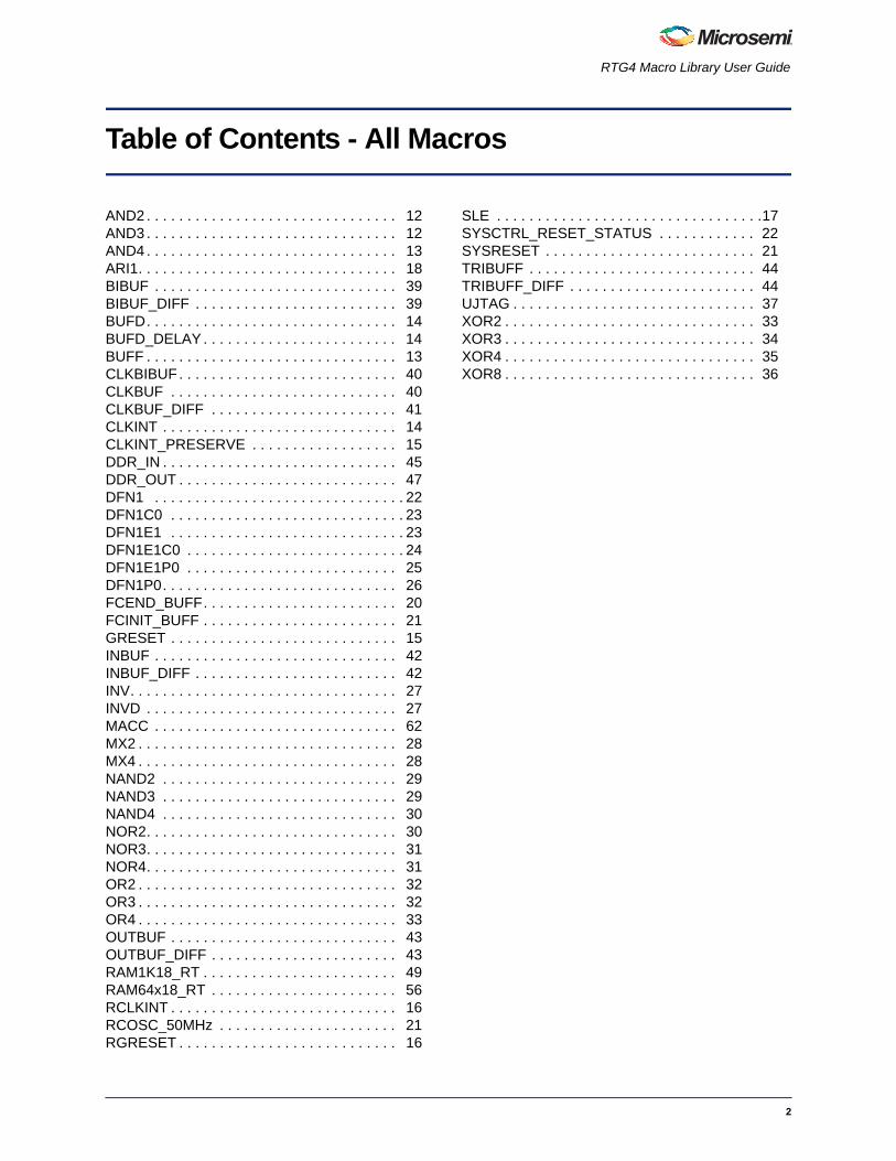
Table of Contents - All Macros
AND2 . . . . . . . . . . . . . . . . . . . . . . . . . . . . . . . 12AND3 . . . . . . . . . . . . . . . . . . . . . . . . . . . . . . . 12AND4 . . . . . . . . . . . . . . . . . . . . . . . . . . . . . . . 13ARI1. . . . . . . . . . . . . . . . . . . . . . . . . . . . . . . . 18BIBUF . . . . . . . . . . . . . . . . . . . . . . . . . . . . . . 39BIBUF_DIFF . . . . . . . . . . . . . . . . . . . . . . . . . 39BUFD. . . . . . . . . . . . . . . . . . . . . . . . . . . . . . . 14BUFD_DELAY . . . . . . . . . . . . . . . . . . . . . . . . 14BUFF . . . . . . . . . . . . . . . . . . . . . . . . . . . . . . . 13CLKBIBUF . . . . . . . . . . . . . . . . . . . . . . . . . . . 40CLKBUF . . . . . . . . . . . . . . . . . . . . . . . . . . . . 40CLKBUF_DIFF . . . . . . . . . . . . . . . . . . . . . . . 41CLKINT . . . . . . . . . . . . . . . . . . . . . . . . . . . . . 14CLKINT_PRESERVE . . . . . . . . . . . . . . . . . . 15DDR_IN . . . . . . . . . . . . . . . . . . . . . . . . . . . . . 45DDR_OUT . . . . . . . . . . . . . . . . . . . . . . . . . . . 47DFN1 . . . . . . . . . . . . . . . . . . . . . . . . . . . . . . . 22DFN1C0 . . . . . . . . . . . . . . . . . . . . . . . . . . . . . 23DFN1E1 . . . . . . . . . . . . . . . . . . . . . . . . . . . . . 23DFN1E1C0 . . . . . . . . . . . . . . . . . . . . . . . . . . . 24DFN1E1P0 . . . . . . . . . . . . . . . . . . . . . . . . . . 25DFN1P0. . . . . . . . . . . . . . . . . . . . . . . . . . . . . 26FCEND_BUFF. . . . . . . . . . . . . . . . . . . . . . . . 20FCINIT_BUFF . . . . . . . . . . . . . . . . . . . . . . . . 21GRESET . . . . . . . . . . . . . . . . . . . . . . . . . . . . 15INBUF . . . . . . . . . . . . . . . . . . . . . . . . . . . . . . 42INBUF_DIFF . . . . . . . . . . . . . . . . . . . . . . . . . 42INV. . . . . . . . . . . . . . . . . . . . . . . . . . . . . . . . . 27INVD . . . . . . . . . . . . . . . . . . . . . . . . . . . . . . . 27MACC . . . . . . . . . . . . . . . . . . . . . . . . . . . . . . 62MX2 . . . . . . . . . . . . . . . . . . . . . . . . . . . . . . . . 28MX4 . . . . . . . . . . . . . . . . . . . . . . . . . . . . . . . . 28NAND2 . . . . . . . . . . . . . . . . . . . . . . . . . . . . . 29NAND3 . . . . . . . . . . . . . . . . . . . . . . . . . . . . . 29NAND4 . . . . . . . . . . . . . . . . . . . . . . . . . . . . . 30NOR2. . . . . . . . . . . . . . . . . . . . . . . . . . . . . . . 30NOR3. . . . . . . . . . . . . . . . . . . . . . . . . . . . . . . 31NOR4. . . . . . . . . . . . . . . . . . . . . . . . . . . . . . . 31OR2 . . . . . . . . . . . . . . . . . . . . . . . . . . . . . . . . 32OR3 . . . . . . . . . . . . . . . . . . . . . . . . . . . . . . . . 32OR4 . . . . . . . . . . . . . . . . . . . . . . . . . . . . . . . . 33OUTBUF . . . . . . . . . . . . . . . . . . . . . . . . . . . . 43OUTBUF_DIFF . . . . . . . . . . . . . . . . . . . . . . . 43RAM1K18_RT . . . . . . . . . . . . . . . . . . . . . . . . 49RAM64x18_RT . . . . . . . . . . . . . . . . . . . . . . . 56RCLKINT . . . . . . . . . . . . . . . . . . . . . . . . . . . . 16RCOSC_50MHz . . . . . . . . . . . . . . . . . . . . . . 21RGRESET . . . . . . . . . . . . . . . . . . . . . . . . . . . 16
SLE . . . . . . . . . . . . . . . . . . . . . . . . . . . . . . . . .17SYSCTRL_RESET_STATUS . . . . . . . . . . . . 22SYSRESET . . . . . . . . . . . . . . . . . . . . . . . . . . 21TRIBUFF . . . . . . . . . . . . . . . . . . . . . . . . . . . . 44TRIBUFF_DIFF . . . . . . . . . . . . . . . . . . . . . . . 44UJTAG . . . . . . . . . . . . . . . . . . . . . . . . . . . . . . 37XOR2 . . . . . . . . . . . . . . . . . . . . . . . . . . . . . . . 33XOR3 . . . . . . . . . . . . . . . . . . . . . . . . . . . . . . . 34XOR4 . . . . . . . . . . . . . . . . . . . . . . . . . . . . . . . 35XOR8 . . . . . . . . . . . . . . . . . . . . . . . . . . . . . . . 36

RTG4 Macro Library User Guide
3
Table of Contents - Combinatorial Logic
AND2 . . . . . . . . . . . . . . . . . . . . . . . . . . . . . . . 12AND3 . . . . . . . . . . . . . . . . . . . . . . . . . . . . . . . 12AND4 . . . . . . . . . . . . . . . . . . . . . . . . . . . . . . . 13ARI1. . . . . . . . . . . . . . . . . . . . . . . . . . . . . . . . 18BUFD. . . . . . . . . . . . . . . . . . . . . . . . . . . . . . . 14BUFD_DELAY . . . . . . . . . . . . . . . . . . . . . . . . 14BUFF . . . . . . . . . . . . . . . . . . . . . . . . . . . . . . . 13INV. . . . . . . . . . . . . . . . . . . . . . . . . . . . . . . . . 27INVD . . . . . . . . . . . . . . . . . . . . . . . . . . . . . . . 27MX2 . . . . . . . . . . . . . . . . . . . . . . . . . . . . . . . . 28MX4 . . . . . . . . . . . . . . . . . . . . . . . . . . . . . . . . 28NAND2 . . . . . . . . . . . . . . . . . . . . . . . . . . . . . 29NAND3 . . . . . . . . . . . . . . . . . . . . . . . . . . . . . 29NAND4 . . . . . . . . . . . . . . . . . . . . . . . . . . . . . 30NOR2. . . . . . . . . . . . . . . . . . . . . . . . . . . . . . . 30NOR3. . . . . . . . . . . . . . . . . . . . . . . . . . . . . . . 31NOR4. . . . . . . . . . . . . . . . . . . . . . . . . . . . . . . 31OR2 . . . . . . . . . . . . . . . . . . . . . . . . . . . . . . . . 32OR3 . . . . . . . . . . . . . . . . . . . . . . . . . . . . . . . . 32OR4 . . . . . . . . . . . . . . . . . . . . . . . . . . . . . . . . 33XOR2. . . . . . . . . . . . . . . . . . . . . . . . . . . . . . . 33XOR3. . . . . . . . . . . . . . . . . . . . . . . . . . . . . . . 34XOR4. . . . . . . . . . . . . . . . . . . . . . . . . . . . . . . 35XOR8. . . . . . . . . . . . . . . . . . . . . . . . . . . . . . . 36
RTG4 Macro Library User Guide
4
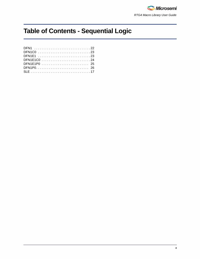
Table of Contents - Sequential Logic
DFN1 . . . . . . . . . . . . . . . . . . . . . . . . . . . . . . . 22DFN1C0 . . . . . . . . . . . . . . . . . . . . . . . . . . . . . 23DFN1E1 . . . . . . . . . . . . . . . . . . . . . . . . . . . . . 23DFN1E1C0 . . . . . . . . . . . . . . . . . . . . . . . . . . . 24DFN1E1P0 . . . . . . . . . . . . . . . . . . . . . . . . . . 25DFN1P0. . . . . . . . . . . . . . . . . . . . . . . . . . . . . 26SLE . . . . . . . . . . . . . . . . . . . . . . . . . . . . . . . . . 17

RTG4 Macro Library User Guide
5
Table of Contents - RAM Blocks
RAM1K18_RT . . . . . . . . . . . . . . . . . . . . . . . . 49RAM64x18_RT . . . . . . . . . . . . . . . . . . . . . . . 56

RTG4 Macro Library User Guide
6
Table of Contents - Math Blocks
MACC . . . . . . . . . . . . . . . . . . . . . . . . . . . . . . 62

RTG4 Macro Library User Guide
7
Table of Contents - I/Os
BIBUF . . . . . . . . . . . . . . . . . . . . . . . . . . . . . . 39BIBUF_DIFF . . . . . . . . . . . . . . . . . . . . . . . . . 39CLKBIBUF . . . . . . . . . . . . . . . . . . . . . . . . . . . 40CLKBUF . . . . . . . . . . . . . . . . . . . . . . . . . . . . 40CLKBUF_DIFF . . . . . . . . . . . . . . . . . . . . . . . 41DDR_IN . . . . . . . . . . . . . . . . . . . . . . . . . . . . . 45DDR_OUT . . . . . . . . . . . . . . . . . . . . . . . . . . . 47INBUF . . . . . . . . . . . . . . . . . . . . . . . . . . . . . . 42INBUF_DIFF . . . . . . . . . . . . . . . . . . . . . . . . . 42OUTBUF . . . . . . . . . . . . . . . . . . . . . . . . . . . . 43OUTBUF_DIFF . . . . . . . . . . . . . . . . . . . . . . . 43TRIBUFF . . . . . . . . . . . . . . . . . . . . . . . . . . . . 44TRIBUFF_DIFF . . . . . . . . . . . . . . . . . . . . . . . 44

RTG4 Macro Library User Guide
8
Table of Contents - Clocking
CLKBIBUF . . . . . . . . . . . . . . . . . . . . . . . . . . . 40CLKBUF . . . . . . . . . . . . . . . . . . . . . . . . . . . . 40CLKBUF_DIFF . . . . . . . . . . . . . . . . . . . . . . . 41CLKINT . . . . . . . . . . . . . . . . . . . . . . . . . . . . . 14CLKINT_PRESERVE . . . . . . . . . . . . . . . . . . 15GRESET . . . . . . . . . . . . . . . . . . . . . . . . . . . . 15RCLKINT . . . . . . . . . . . . . . . . . . . . . . . . . . . . 16RCOSC_50MHz . . . . . . . . . . . . . . . . . . . . . . 21RGRESET . . . . . . . . . . . . . . . . . . . . . . . . . . . 16

RTG4 Macro Library User Guide
9
Table of Contents - Special
FCEND_BUFF. . . . . . . . . . . . . . . . . . . . . . . . 20FCINIT_BUFF . . . . . . . . . . . . . . . . . . . . . . . . 21SYSCTRL_RESET_STATUS . . . . . . . . . . . . 22SYSRESET . . . . . . . . . . . . . . . . . . . . . . . . . . 21UJTAG. . . . . . . . . . . . . . . . . . . . . . . . . . . . . . 37

Introduction
This macro library guide supports the RTG4 family. See the Microsemi website for macro guides for other families.
This guide follows a naming convention for sequential macros that is unambiguous and extensible, making it possible to understand the function of the macros by their name alone.
The first two mandatory characters of the macro name will indicate the basic macro function:
• DF - D-type flip-flop
The next mandatory character indicates the output polarity:
• I - output inverted (QN with bubble)
• N - output non-inverted (Q without bubble)
The next mandatory number indicates the polarity of the clock or gate:
• 1 - rising edge triggered flip-flop or transparent high latch (non-bubbled)
• 0 - falling edge triggered flip-flop or transparent low latch (bubbled)
The next two optional characters indicate the polarity of the Enable pin, if present:
• E0 - active low enable (bubbled)
• E1 - active high enable (non-bubbled)
The next two optional characters indicate the polarity of the asynchronous Preset pin, if present:
• P0 - active low asynchronous preset (bubbled)
• P1 - active high asynchronous preset (non-bubbled)
The next two optional characters indicate the polarity of the asynchronous Clear pin, if present:
• C0 - active low asynchronous clear (bubbled)
• C1 - active high asynchronous clear (non-bubbled)
All sequential and combinatorial macros (except MX4 and XOR8) use one logic element in the
RTG4 family.
As an example, the macro DFN1E1C0 indicates a D-type flip-flop (DF) with a non-inverted (N) Q output, positive-edge triggered (1), with Active High Clock Enable (E1) and Active Low Asychronous Clear (C0). See Figure 1.
10

Figure 1 • Naming Convention
11

RTG4 Macro Library User Guide
AND22-Input AND
Truth Table
AND33-Input AND
Truth Table
Figure 2 • AND2
Inputs Output
A, B Y
A B Y
X 0 0
0 X 0
1 1 1
Figure 3 • AND3
Input Output
A, B, C Y
A B C Y
X X 0 0
X 0 X 0
0 X X 0
1 1 1 1
A
B
Y
Y
C
B
A
12

RTG4 Macro Library User Guide
AND44-Input AND
Truth Table
BUFFBuffer
Truth Table
Figure 4 • AND4
Input Output
A, B, C, D Y
A B C D Y
X X X 0 0
X X 0 X 0
X 0 X X 0
0 X X X 0
1 1 1 1 1
Figure 5 • BUFF
Input Output
A Y
A Y
0 0
1 1
Y
C
B
A
D
A Y
13

RTG4 Macro Library User Guide
BUFDBuffer. Note that Compile optimization will not remove this macro.
Truth Table
BUFD_DELAYBuffer. Note that Compile optimization will not remove this macro.
Truth Table
CLKINTMacro used to route an internal fabric signal to global network.
Figure 6 • BUFD
Input Output
A Y
A Y
0 0
1 1
Figure 7 • BUFD
Input Output
A Y
A Y
0 0
1 1
Figure 8 • CLKINT
A Y
A Y
A Y
14
RTG4 Macro Library User Guide
Truth Table
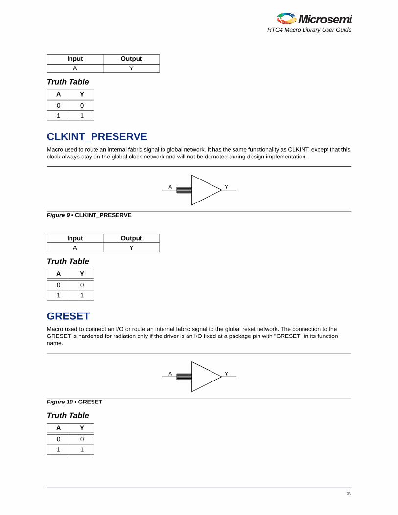
CLKINT_PRESERVEMacro used to route an internal fabric signal to global network. It has the same functionality as CLKINT, except that this clock always stay on the global clock network and will not be demoted during design implementation.
Truth Table
GRESETMacro used to connect an I/O or route an internal fabric signal to the global reset network. The connection to the GRESET is hardened for radiation only if the driver is an I/O fixed at a package pin with "GRESET" in its function name.
Truth Table
Input Output
A Y
A Y
0 0
1 1
Figure 9 • CLKINT_PRESERVE
Input Output
A Y
A Y
0 0
1 1
Figure 10 • GRESET
A Y
0 0
1 1
A Y
A Y
15

RTG4 Macro Library User Guide
RCLKINTMacro used to route an internal fabric signal to a row global buffer, thus creating a local clock.
Truth Table
RGRESETMacro used to route a triplicated fabric signal to a row global buffer and create a local reset. The three input bits must be driven by three separate logic cones replicating the paths from the source registers.
Truth Table
Figure 11 • RCLKINT
Input Output
A Y
A Y
0 0
1 1
Figure 12 • RGRESET
A[2] A[1] A[0] Y
X 0 0 0
0 X 0 0
0 0 X 0
X 1 1 1
1 X 1 1
1 1 X 1
A Y
A[2]
A[1]
A[0]
16
RTG4 Macro Library User Guide
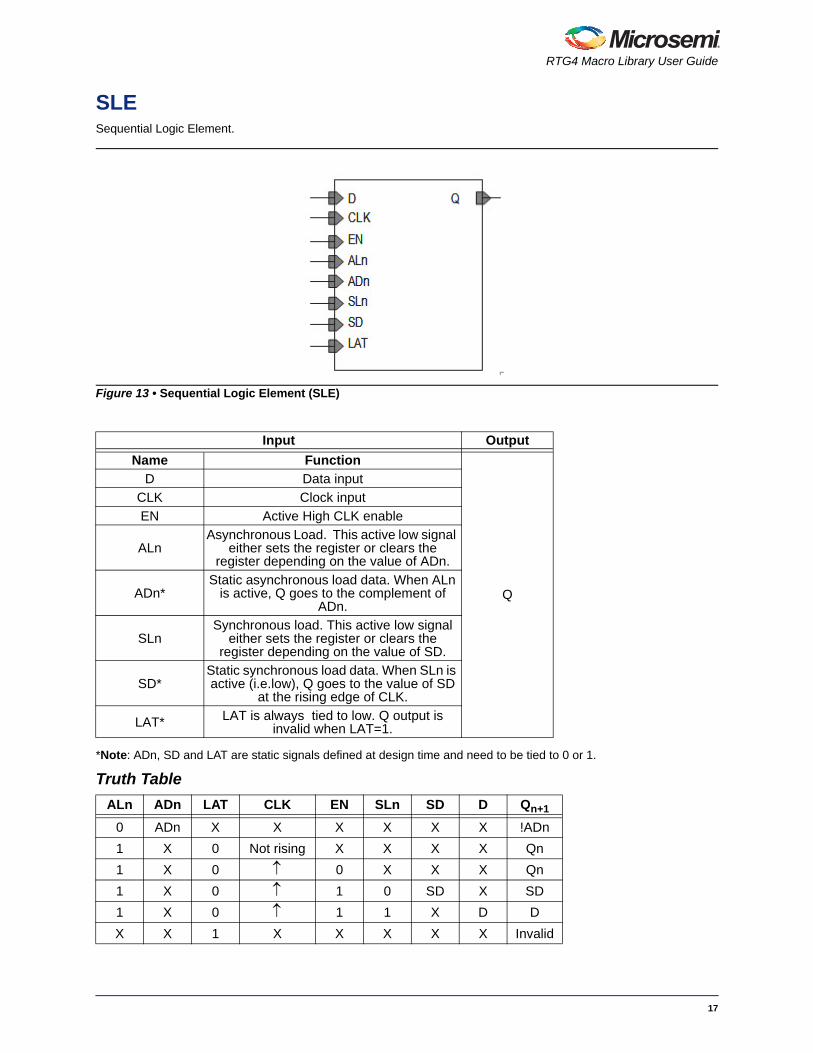
SLESequential Logic Element.
*Note: ADn, SD and LAT are static signals defined at design time and need to be tied to 0 or 1.
Truth Table
Figure 13 • Sequential Logic Element (SLE)
Input Output
Name Function
Q
D Data input
CLK Clock input
EN Active High CLK enable
ALnAsynchronous Load. This active low signal
either sets the register or clears the register depending on the value of ADn.
ADn*Static asynchronous load data. When ALn
is active, Q goes to the complement of ADn.
SLnSynchronous load. This active low signal
either sets the register or clears the register depending on the value of SD.
SD*Static synchronous load data. When SLn is active (i.e.low), Q goes to the value of SD
at the rising edge of CLK.
LAT* LAT is always tied to low. Q output is invalid when LAT=1.
ALn ADn LAT CLK EN SLn SD D Qn+1
0 ADn X X X X X X !ADn
1 X 0 Not rising X X X X Qn
1 X 0 0 X X X Qn
1 X 0 1 0 SD X SD
1 X 0 1 1 X D D
X X 1 X X X X X Invalid
17

RTG4 Macro Library User Guide
ARI1The ARI1 macro is responsible for representing all arithmetic operations in the pre-layout phase
The ARI1 cell has a 20bit INIT string parameter that is used to configure its functionality. The interpretation of the 16 LSB of the INIT string is shown in the table below. F0 is the value of Y when A = 0 and F1 is the value of Y when A = 1.
Figure 14 • ARI1
Input Output
A, B, C, D, FCI Y, S, FCO
Table 1 • Interpretation of 16 LSB of the INIT String for ARI1
ADCB Y
0000 INIT[0] F0
0001 INIT[1]
0010 INIT[2]
0011 INIT[3]
0100 INIT[4]
0101 INIT[5]
0110 INIT[6]
0111 INIT[7]
1000 INIT[8] F1
1001 INIT[9]
1010 INIT[10]
1011 INIT[11]
1100 INIT[12]
1101 INIT[13]
1110 INIT[14]
1111 INIT[15]
AB
C
D
FCI
Y
S
FCO
18

RTG4 Macro Library User Guide
The 4 MSB of the INIT string controls the output of the carry bits. The carry is generated using carry propagation and generation bits, which are evaluated according to the tables below.
Table 2 • Truth Table for S
Y FCI S
0 0 0
0 1 1
1 0 1
1 1 0
Figure 15 • ARI1 Logic
Table 3 • ARI1 INIT[17:16] String Interpretation
INIT[17] INIT[16] G
0 0 0
0 1 F0
1 0 1
1 1 F1
19

RTG4 Macro Library User Guide
FCEND_BUFFBuffer, driven by the FCO pin of the last macro in the Carry-Chain.
Truth Table
Table 4 • ARI1 INIT[19:18] String Interpretation
INIT[19] INIT[18] P
0 0 0
0 1 Y
1 X 1
Table 5 • FCO Truth Table
P G FCI FCO
0 G X G
1 X FCI FCI
Figure 16 • FCEND_BUFF
Input Output
A Y
A Y
0 0
1 1
A Y
20

RTG4 Macro Library User Guide
FCINIT_BUFFBuffer, used to initialize the FCI pin of the first macro in the Carry-Chain.
RCOSC_50MHzThe RCOSC_50MHz oscillator is an RC oscillator that provides a free running clock of 50MHz at CLKOUT.
SYSRESETSYSRESET is a special-purpose macro. The Output POWER_ON_RESET_N goes low at power up and when DEVRST_N goes low.
Figure 17 • FCINIT_BUFF
Input Output
A Y
Figure 18 • RCOSC_50MHz
Figure 19 • SYSRESET
Input Output
DEVRST_N POWER_ON_RESET_N
A Y
CLKOUT
21

RTG4 Macro Library User Guide
Truth Table
SYSCTRL_RESET_STATUSThis is a special-purpose macro to check the status of the System Controller. The output port RESET_STATUS goes high if the System Controller is in reset.This macro is enabled by selecting the "Enable System Controller Suspend Mode" option in the "Configure Programming Bitstream Settings" tool within Libero. After programming, the device will enter "System Controller Suspend Mode" if TRSTB is tied low during device power up.
This macro is not supported in simulation.
DFN1D-Type Flip-Flop
Truth Table
DEVRST_N POWER_ON_RESET_N
0 0
1 1
Figure 20 • SYSCTRL_RESET_STATUS
Figure 21 • DFN1
Input Output
D, CLK Q
CLK D Qn+1
not Rising X Qn
D D
Q
CLK
D
22

RTG4 Macro Library User Guide
DFN1C0D-Type Flip-Flop with active low Clear
Truth Table
DFN1E1D-Type Flip-Flop with active high Enable
Truth Table
Figure 22 • DFN1C0
Input Output
D, CLK, CLR Q
CLR CLK D Qn+1
0 X X 0
1 not Rising X Qn
1 D D
Figure 23 • DFN1E1
Input Output
D, E, CLK Q
E CLK D Qn+1
0 X X Qn
1 not Rising X Qn
1 D D
Q
CLR
CLK
D
Q
CLK
E
D
23
RTG4 Macro Library User Guide
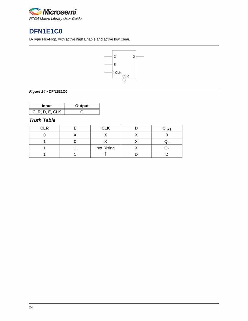
DFN1E1C0D-Type Flip-Flop, with active high Enable and active low Clear.
Truth Table
Figure 24 • DFN1E1C0
Input Output
CLR, D, E, CLK Q
CLR E CLK D Qn+1
0 X X X 0
1 0 X X Qn
1 1 not Rising X Qn
1 1 D D
Q
CLRCLK
E
D
24

RTG4 Macro Library User Guide
DFN1E1P0D-Type Flip-Flop with active high Enable and active low Preset.
Truth Table
Figure 25 • DFN1E1P0
Input Output
D, E, PRE, CLK Q
PRE E CLK D Qn+1
0 X X X 1
1 0 X X Qn
1 1 not Rising X Qn
1 1 D D
QPRE
CLK
E
D
25

RTG4 Macro Library User Guide
DFN1P0D-Type Flip-Flop with active low Preset.
Truth Table
Figure 26 • DFN1P0
Input Output
D, PRE, CLK Q
PRE CLK D Qn+1
0 X X 1
1 not Rising X Qn
1 D D
Q
PRE
CLK
D
26
RTG4 Macro Library User Guide
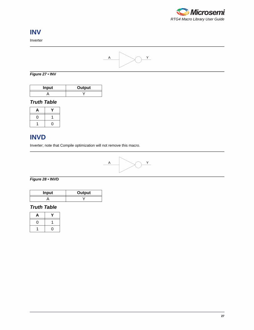
INVInverter
Truth Table
INVDInverter; note that Compile optimization will not remove this macro.
Truth Table
Figure 27 • INV
Input Output
A Y
A Y
0 1
1 0
Figure 28 • INVD
Input Output
A Y
A Y
0 1
1 0
YA
YA
27

RTG4 Macro Library User Guide
MX22 to 1 Multiplexer
Truth Table
MX44 to 1 Multiplexer
This macro uses two logic modules.
Truth Table
Figure 29 • MX2
Input Output
A, B, S Y
A B S Y
A X 0 A
X B 1 B
Figure 30 • MX4
Input Output
D0, D1, D2, D3, S0, S1 Y
D3 D2 D1 D0 S1 S0 Y
X X X D0 0 0 D0
X X D1 X 0 1 D1
X D2 X X 1 0 D2
D3 X X X 1 1 D3
S
Y
B
A
S0
Y
D3
D0
D1
D2
S1
28

RTG4 Macro Library User Guide
NAND22-Input NAND
Truth Table
NAND33-Input NAND
Truth Table
Figure 31 • NAND2
Input Output
A, B Y
A B Y
X 0 1
0 X 1
1 1 0
Figure 32 • NAND3
Input Output
A, B, C Y
A B C Y
X X 0 1
X 0 X 1
0 X X 1
1 1 1 0
B
YA
B
C
Y
A
29

RTG4 Macro Library User Guide
NAND44-input NAND
Truth Table
NOR22-input NOR
Truth Table
Figure 33 • NAND4
Input Output
A, B, C, D Y
A B C D Y
X X X 0 1
X X 0 X 1
X 0 X X 1
0 X X X 1
1 1 1 1 0
Figure 34 • NOR2
Input Output
A, B Y
A B Y
0 0 1
X 1 0
1 X 0
B
C
Y
A
D
A
B
Y
30

RTG4 Macro Library User Guide
NOR33-input NOR
Truth Table
NOR44-input NOR
Truth Table
Figure 35 • NOR3
Input Output
A, B, C Y
A B C Y
0 0 0 1
X X 1 0
X 1 X 0
1 X X 0
Figure 36 • NOR4
Input Output
A, B, C, D Y
A B C D Y
0 0 0 0 1
1 X X X 0
X 1 X X 0
X X 1 X 0
X X X 1 0
Y
C
B
A
Y
D
B
A
C
31
RTG4 Macro Library User Guide
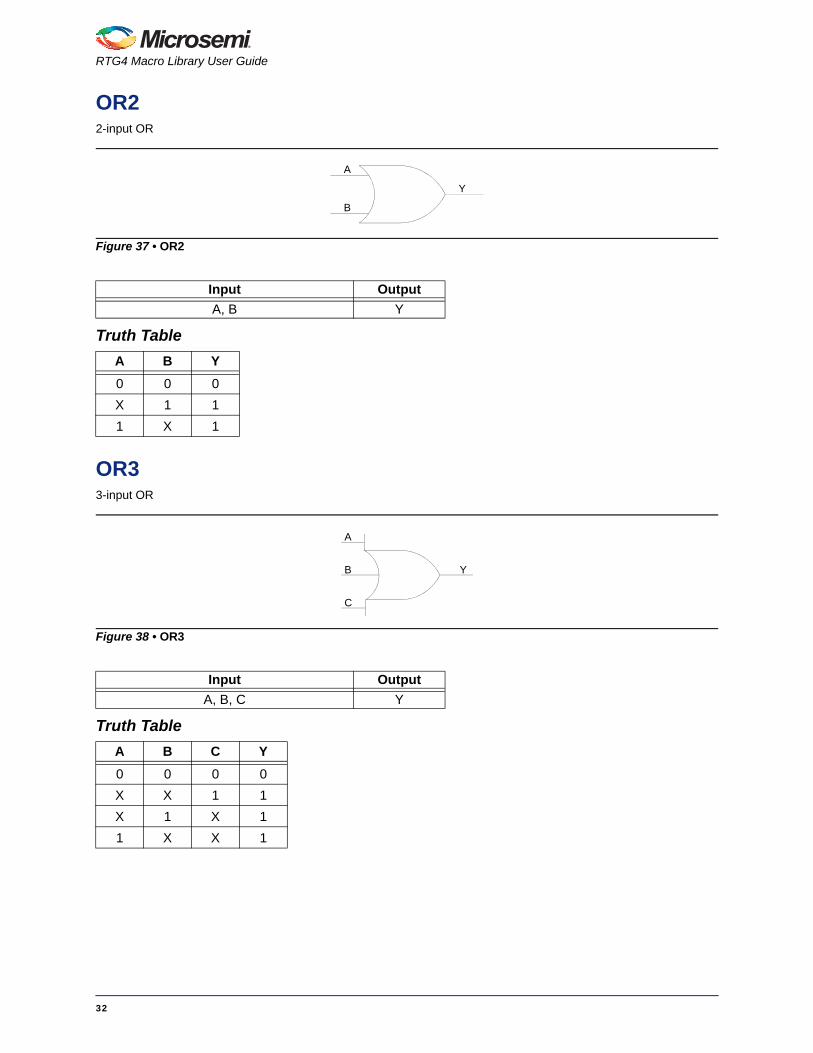
OR22-input OR
Truth Table
OR33-input OR
Truth Table
Figure 37 • OR2
Input Output
A, B Y
A B Y
0 0 0
X 1 1
1 X 1
Figure 38 • OR3
Input Output
A, B, C Y
A B C Y
0 0 0 0
X X 1 1
X 1 X 1
1 X X 1
A
Y
B
Y
C
B
A
32

RTG4 Macro Library User Guide
OR44-input OR
Truth Table
XOR22-input XOR
Truth Table
Figure 39 • OR4
Input Output
A, B, C, D Y
A B C D Y
0 0 0 0 0
1 X X X 1
X 1 X X 1
X X 1 X 1
X X X 1 1
Figure 40 • XOR2
Input Output
A, B Y
A B Y
0 0 0
0 1 1
1 0 1
1 1 0
Y
D
B
A
C
Y
B
A
33

RTG4 Macro Library User Guide
XOR33-input XOR
Truth Table
Figure 41 • XOR3
Input Output
A, B, C Y
A B C Y
0 0 0 0
1 0 0 1
0 1 0 1
1 1 0 0
0 0 1 1
1 0 1 0
0 1 1 0
1 1 1 1
Y
C
A
B
34

RTG4 Macro Library User Guide
XOR44-input XOR
Truth Table
Figure 42 • XOR4
Input Output
A, B, C, D Y
A B C D Y
0 0 0 0 0
0 0 0 1 1
0 0 1 0 1
0 0 1 1 0
0 1 0 0 1
0 1 0 1 0
0 1 1 0 0
0 1 1 1 1
1 0 0 0 1
1 0 0 1 0
1 0 1 0 0
1 0 1 1 1
1 1 0 0 0
1 1 0 1 1
1 1 1 0 1
1 1 1 1 0
YC
AB
D
35

RTG4 Macro Library User Guide
XOR88-input XOR
This macro uses two logic modules.
Truth Table If you have an odd number of inputs that are High, the output is High (1).
If you have an even number of inputs that are High, the output is Low (0).
For example:
Figure 43 • XOR8
Input Output
A, B, C, D, E, F, G, H Y
A B C D E F G H Y
0 0 0 0 0 0 0 0 0
0 0 0 0 0 0 0 1 1
0 0 0 0 0 0 1 1 0
A
Y
B
C
E
F
G
H
D
36

RTG4 Macro Library User Guide
UJTAGThe UJTAG macro is a special purpose macro. It allows access to the user JTAG circuitry on board the chip.
You must instantiate a UJTAG macro in your design if you plan to make use of the user JTAG feature. The TMS, TDI, TCK, TRSTB and TDO pins of the macro must be connected to top level ports of the design.
Figure 44 • UJTAG
Table 6: Ports and Descriptions
Port Direction Polarity Description
UIREG[7:0]
Output —
This 8-bit bus carries the contents of the JTAG instruction register of each device. Instruction values 16 to 127 are not reserved and can be employed as user-defined instructions
URSTB
Output Low
URSTB is an Active Low signal and is asserted when the TAP controller is in Test-Logic-Reset mode. URSTB is asserted at power-up, and a power-on reset signal resets the TAP controller state.
UTDI Output — This port is directly connected to the TAP's TDI signal
UTDO
Input —
This port is the user TDO output. Inputs to the UTDO port are sent to the TAP TDO output MUX when the IR addess is in user range.
UDRSH Output High Active High signal enabled in the Shift_DR TAP state.
UDRCAP Output High Active High signal enabled in the Capture_DR_TAP state.
UDRCK Output — This port is directly connected to the TAP's TCK signal.
UDRUPD Output High Active High signal enabled in the Update_DR_TAP state.
UTDOTMSTDITCKTRSTB
URSTBUDRCKUDRCAPUDRSHUDRUPDUTDI
UIREG[7:0]
37

RTG4 Macro Library User Guide
TCK
Input —
Test ClockSerial input for JTAG boundary scan, ISP, and UJTAG. The TCK pin does not have an internal pull-up/pull-down resistor. Connect TCK to GND or +3.3 V through a resistor (500-1 KΩ) placed closed to the FPGA pin to prevent totem-pole current on the input buffer and TMS from entering into an undesired state.If JTAG is not used, connect it to GND.
TDI
Input —
Test Data in. Serial input for JTAG boundary scan. There is an internal weak pull-up resistor on the TDI pin.
TDO
Output —
Test Data Out. Serial output for JTAG boundary scan. The TDO pin does not have an internal pull-up/pull-down resistor.
TMS
Input —
Test mode select. The TMS pin controls the use of the IEEE1532 boundary scan pins (TCK, TDI, TDO, and TRST). There is an internal weak pull-up resistor on the TMS pin.
TRSTB
Input Low
Test reset. The TRSTB pin is an active low input . It synchronously initializes (or resets) the boundary scan circuitry. There is an internal weak pull-up resistor on the TRSTB pin.To hold the JTAG in reset mode and prevent it from entering into undesired states in critical applications, connect TRSTB to GND through a 1 KΩ resistor (placed close to the FPGA pin).
Table 6: Ports and Descriptions (Continued)
Port Direction Polarity Description
38

RTG4 Macro Library User Guide
BIBUFBidirectional Buffer
Truth Table
BIBUF_DIFFBidirectional Buffer, Differential I/O
Truth Table
Figure 45 • BIBUF
Input Output
D, E, PAD PAD, Y
MODE E D PAD Y
OUTPUT 1 D D D
INPUT 0 X Z X
INPUT 0 X PAD PAD
Figure 46 • BIBUF_DIFF
Input Output
D, E, PADP, PADN PADP, PADN, Y
MODE E D PADP PADN Y
OUTPUT 1 0 0 1 0
OUTPUT 1 1 1 0 1
INPUT 0 X Z Z X
INPUT 0 X 0 0 X
INPUT 0 X 1 1 X
INPUT 0 X 0 1 0
INPUT 0 X 1 0 1
D PADE
Y
DPADPE
YPADN
39
RTG4 Macro Library User Guide
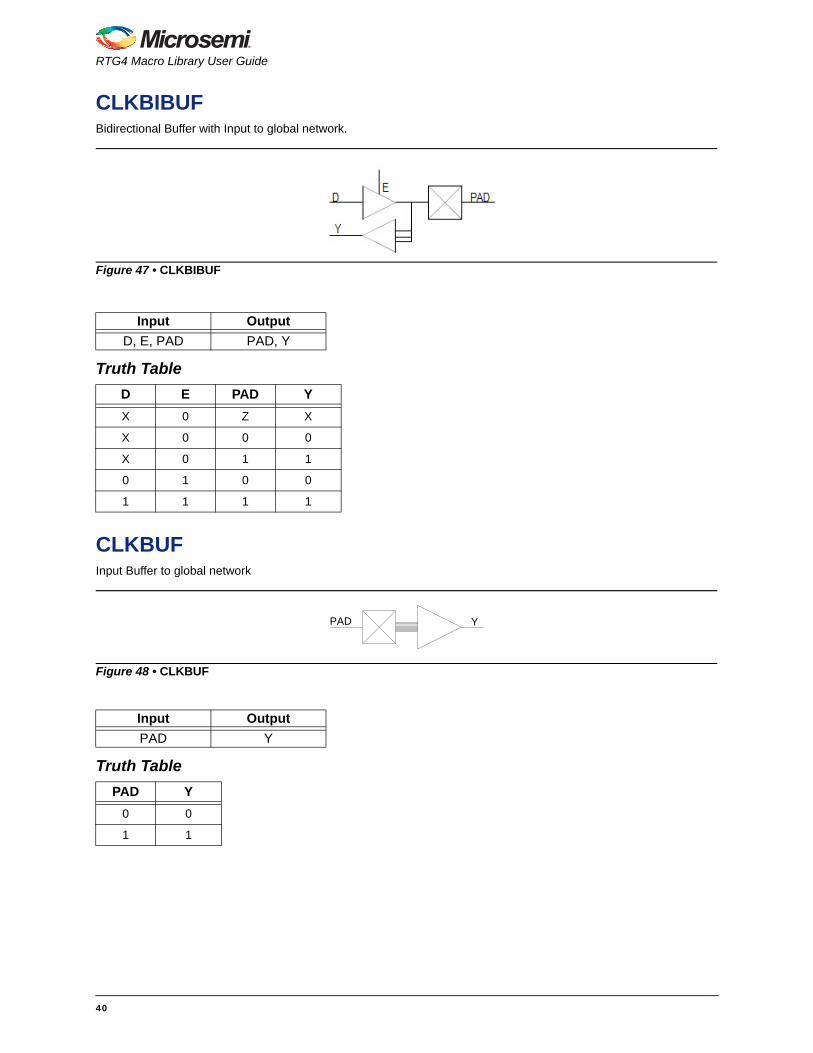
CLKBIBUFBidirectional Buffer with Input to global network.
Truth Table
CLKBUFInput Buffer to global network
Truth Table
Figure 47 • CLKBIBUF
Input Output
D, E, PAD PAD, Y
D E PAD Y
X 0 Z X
X 0 0 0
X 0 1 1
0 1 0 0
1 1 1 1
Figure 48 • CLKBUF
Input Output
PAD Y
PAD Y
0 0
1 1
YPAD
40

RTG4 Macro Library User Guide
CLKBUF_DIFFDifferential I/O macro to global network, Differential I/O
Truth Table
Figure 49 • INBUF_DIFF
Input Output
PADP, PADN Y
PADP PADN Y
Z Z Y
0 0 X
1 1 X
0 1 0
1 0 1
YPADP
PADN
41

RTG4 Macro Library User Guide
INBUFInput Buffer
Truth Table
INBUF_DIFFInput Buffer, Differential I/O
Truth Table
Figure 50 • INBUF
Input Output
PAD Y
PAD Y
Z X
0 0
1 1
Figure 51 • INBUF_DIFF
Input Output
PADP, PADN Y
PADP PADN Y
Z Z X
0 0 X
1 1 X
0 1 0
1 0 1
YPAD
YPADP
PADN
42

RTG4 Macro Library User Guide
OUTBUFOutput buffer
Truth Table
OUTBUF_DIFFOutput buffer, Differential I/O
Truth Table
Figure 52 • OUTBUF
Input Output
D PAD
D PAD
0 0
1 1
Figure 53 • OUTBUF_DIFF
Input Output
D PADP, PADN
D PADP PADN
0 0 1
1 1 0
PADD
PADPD
PADN
43

RTG4 Macro Library User Guide
TRIBUFFTristate output buffer
Truth Table
TRIBUFF_DIFFTristate output buffer, Differential I/O
Truth Table
Figure 54 • TRIBUFF
Input Output
D, E PAD
D E PAD
X 0 Z
D 1 D
Figure 55 • TRIBUFF_DIFF
Input Output
D, E PADP, PADN
D E PADP PADN
X 0 Z Z
0 1 0 1
1 1 1 0
D PADE
DPADPE
PADN
44

RTG4 Macro Library User Guide
DDR_INThe DDR_IN macro is available for both pre-layout and post-layout simulation flows. It consists of two SLE macros and a latch.
The iinput D must be connected to an I/O.
*Note: ADn and SD are static inputs defined at design time and need to be tied to 0 or 1.
Figure 56 • DDR_IN
Input Output
D, CLK, EN, ALn, ADn, SLn, SD QR, QF
Input Output
Name Function Name Function
D Data QR Q (Rising Edge)
CLK Clock QF Q (Falling Edge)
EN Enable
ALn Asynchronous Load (Active Low)
ADn* Asynchronous Data (Active Low)
SLn Synchronous Load (Active Low)
SD* Synchronous Data
45
RTG4 Macro Library User Guide
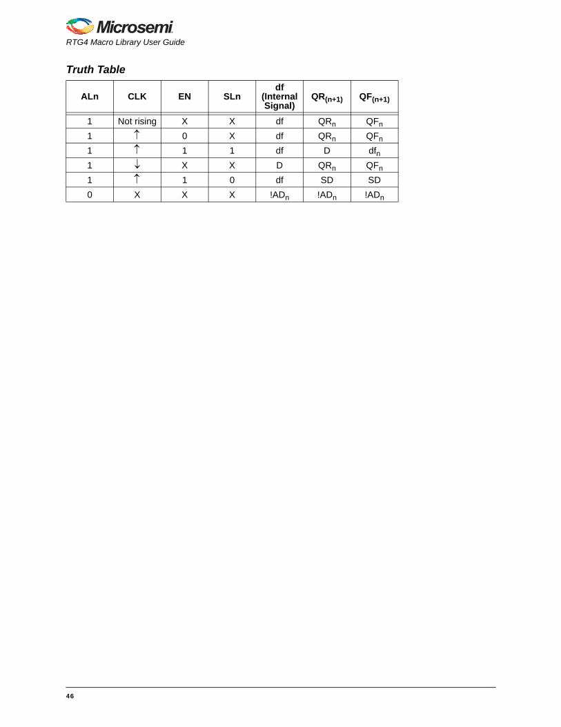
Truth Table
ALn CLK EN SLndf
(Internal Signal)
QR(n+1) QF(n+1)
1 Not rising X X df QRn QFn
1 0 X df QRn QFn
1 1 1 df D dfn1 X X D QRn QFn
1 1 0 df SD SD
0 X X X !ADn !ADn !ADn
46
RTG4 Macro Library User Guide
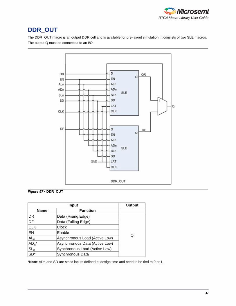
DDR_OUTThe DDR_OUT macro is an output DDR cell and is available for pre-layout simulation. It consists of two SLE macros.
The output Q must be connected to an I/O.
*Note: ADn and SD are static inputs defined at design time and need to be tied to 0 or 1.
Figure 57 • DDR_OUT
Input Output
Name Function
DR Data (Rising Edge)
Q
DF Data (Falling Edge)
CLK Clock
EN Enable
ALn Asynchronous Load (Active Low)
ADn* Asynchronous Data (Active Low)
SLn Synchronous Load (Active Low)
SD* Synchronous Data
47

RTG4 Macro Library User Guide
Truth Table
ALn CLK EN SLn Qn+1
1 not rising X X Qn
1 0 X Qn
1 1 1 DRn
1 1 1 DFn
1 1 0 SD
0 X X X !ADn
48
RTG4 Macro Library User Guide
RAM1K18_RT The RAM1K18_RT block contains 24,576 (18,432 with ECC) memory bits and is a true dual-port memory. The RAM1K18_RT memory can also be configured in two-port mode. All read/write operations to the RAM1K18_RT memory are synchronous. To improve the read-data delay, an optional pipeline register at the output is available. Besides the feed-through write mode option to enable immediate access to the write-data, RAM1K18_RT has a Read-before-write option in the dual-port mode. RAM1K18_RT also adds a Read-enable control to both dual-port and two-port modes. The RAM1K18_RT memory has two data ports which can be independently configured in any combination shown below.
1. ECC Dual-Port RAM with the following configuration:
– 1Kx18 on both ports
2. Non-ECC Dual-Port RAM with the following configurations:
– Any of 1Kx18 or 2Kx9 on each port
– 2Kx12 on both ports
3. ECC Two-Port RAM with the following configurations:
– Any of 512x36 or 1Kx18 on each port
4. Non-ECC Two-Port RAM with the following configurations:
– Any of 512x36, 1Kx18 or 2Kx9 on each port
– 2Kx12 on both ports
FunctionalityThe main features of the RAM1K18_RT memory block are as follows:
• A RAM1K18_RT block has 18,432 bits with ECC and 24,576 bits without ECC.
• A RAM1K18_RT block provides two independent data ports A and B.
• RAM1K18_RT has an ECC dual-port mode, for which both ports have word widths equal to 18 bits.
– 1Kx18/1Kx18
• In non-ECC dual-port mode, each port can be independently configured to any of the following depth/width: 1Kx18 or 2Kx9. In addition, both ports can be configured to 2Kx12. There are 4 unique combinations of non-ECC dual-port aspect ratios:
– 1Kx18/1Kx18
– 1Kx18/2Kx9
– 2Kx9/1Kx18
– 2Kx12/2Kx12
• RAM1K18_RT also has a two-port mode. In this case, Port A will become the read port and Port B becomes the write port.
• RAM1K18_RT has an ECC two-port mode, for which both ports have word widths equal to either 36 or 18 bits. There are 4 unique combinations of ECC two-port aspect ratios:
– 512x36/512x36
– 512x36/1Kx18
– 1Kx18/512x36
– 1Kx18/1Kx18
• In non-ECC two-port mode, each port can be independently configured to any of the following depth/width: 512x36, 1Kx18, or 2Kx9. In addition, both ports can be configured to 2Kx12. There are 9 unique combinations of non-ECC two-port aspect ratios:
– 512x36/512x36
– 512x36/1Kx18
– 512x36/2Kx9
– 1Kx18/512x36
– 1Kx18/1Kx18
49

RTG4 Macro Library User Guide
– 1Kx18/2Kx9
– 2Kx9/512x36
– 2Kx9/1Kx18
– 2Kx12/2Kx12
• RAM1K18_RT performs synchronous operation for setting up the address as well as writing and reading the data.
• RAM1K18_RT has a Read-enable control to both dual-port and two-port modes.
• The address, data, block-port select, write-enable and read-enable inputs are registered.
• An optional pipeline register with a separate enable and synchronous-reset is available at the read-data port to improve the clock-to-out delay.
• The registers in RAM1K18_RT block have an option to mitigate Single-event transients.
• There is an independent clock for each port. The memory will be triggered at the rising edge of the clock.
• The true dual-port mode supports an optional Read-before-write mode or a feed-through write mode, where the write-data also appears on the corresponding read-data port.
• Read from both ports at the same location is allowed.
• Read and write on the same location at the same time results in unknown data to be read. There is no collision prevention or detection. However, correct data is expected to be written into the memory.
• When ECC is enabled, each port of the RAM1K18_RT memory can raise flags to indicate single-bit-correct and double-bit-detect.
Figure 58 shows a simplified block diagram of the RAM1K18_RT memory block and Table 8 gives the port descriptions. The simplified block illustrates the two independent data ports, the read-data pipeline registers, read-before-write selection and feed-through multiplexors.
Figure 58 • Simplified Block Diagram of RAM1K18_RT
50
RTG4 Macro Library User Guide
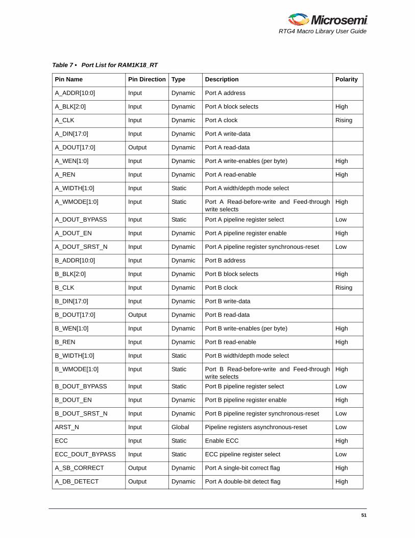
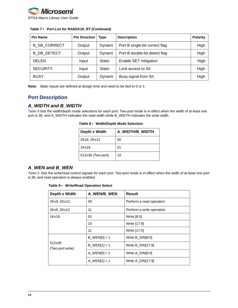
Table 7 • Port List for RAM1K18_RT
Pin Name Pin Direction Type Description Polarity
A_ADDR[10:0] Input Dynamic Port A address
A_BLK[2:0] Input Dynamic Port A block selects High
A_CLK Input Dynamic Port A clock Rising
A_DIN[17:0] Input Dynamic Port A write-data
A_DOUT[17:0] Output Dynamic Port A read-data
A_WEN[1:0] Input Dynamic Port A write-enables (per byte) High
A_REN Input Dynamic Port A read-enable High
A_WIDTH[1:0] Input Static Port A width/depth mode select
A_WMODE[1:0] Input Static Port A Read-before-write and Feed-throughwrite selects
High
A_DOUT_BYPASS Input Static Port A pipeline register select Low
A_DOUT_EN Input Dynamic Port A pipeline register enable High
A_DOUT_SRST_N Input Dynamic Port A pipeline register synchronous-reset Low
B_ADDR[10:0] Input Dynamic Port B address
B_BLK[2:0] Input Dynamic Port B block selects High
B_CLK Input Dynamic Port B clock Rising
B_DIN[17:0] Input Dynamic Port B write-data
B_DOUT[17:0] Output Dynamic Port B read-data
B_WEN[1:0] Input Dynamic Port B write-enables (per byte) High
B_REN Input Dynamic Port B read-enable High
B_WIDTH[1:0] Input Static Port B width/depth mode select
B_WMODE[1:0] Input Static Port B Read-before-write and Feed-throughwrite selects
High
B_DOUT_BYPASS Input Static Port B pipeline register select Low
B_DOUT_EN Input Dynamic Port B pipeline register enable High
B_DOUT_SRST_N Input Dynamic Port B pipeline register synchronous-reset Low
ARST_N Input Global Pipeline registers asynchronous-reset Low
ECC Input Static Enable ECC High
ECC_DOUT_BYPASS Input Static ECC pipeline register select Low
A_SB_CORRECT Output Dynamic Port A single-bit correct flag High
A_DB_DETECT Output Dynamic Port A double-bit detect flag High
51
RTG4 Macro Library User Guide
Note: Static inputs are defined at design time and need to be tied to 0 or 1.
Port Description
A_WIDTH and B_WIDTHTable 8 lists the width/depth mode selections for each port. Two-port mode is in effect when the width of at least one port is 36, and A_WIDTH indicates the read width while B_WIDTH indicates the write width.
A_WEN and B_WENTable 9 lists the write/read control signals for each port. Two-port mode is in effect when the width of at least one port is 36, and read operation is always enabled.
Pin Name Pin Direction Type Description Polarity
B_SB_CORRECT Output Dynami Port B single-bit correct flag High
B_DB_DETECT Output Dynami Port B double-bit detect flag High
DELEN Input Static Enable SET mitigation High
SECURITY Input Static Lock access to SII High
BUSY Output Dynami Busy signal from SII High
Table 8 • Width/Depth Mode Selection
Depth x Width A_WIDTH/B_WIDTH
2Kx9, 2Kx12 00
1Kx18 01
512x36 (Two-port) 10
Table 9 • Write/Read Operation Select
Depth x Width A_WEN/B_WEN Result
2Kx9, 2Kx12, 00 Perform a read operation
2Kx9, 2Kx12 11 Perform a write operation
1Kx18 01 Write [8:0]
10 Write [17:9]
11 Write [17:0]
512x36
(Two-port write)
B_WEN[0] = 1 Write B_DIN[8:0]
B_WEN[1] = 1 Write B_DIN[17:9]
A_WEN[0] = 1 Write A_DIN[8:0]
A_WEN[1] = 1 Write A_DIN[17:9]
Table 7 • Port List for RAM1K18_RT (Continued)
52

RTG4 Macro Library User Guide
A_ADDR and B_ADDRTable 10 lists the address buses for the two ports. 11 bits are needed to address the 2K independent locations in x9 mode. In wider modes, fewer address bits are used. The required bits are MSB justified and unused LSB bits must be tied to 0. A_ADDR is synchronized by A_CLK while B_ADDR is synchronized to B_CLK. Two-port mode is in effect when the width of at least one port is 36, and A_ADDR provides the read-address while B_ADDR provides the write-address.
A_DIN and B_DINTable 11 lists the data input buses for the two ports. The required bits are LSB justified and unused MSB bits must be tied to 0. Two-port mode is in effect when the width of at least one port is 36, and A_DIN provides the MSB of the write-data while B_DIN provides the LSB of the write-data.
A_DOUT and B_DOUTTable 12 lists the data output buses for the two ports. The required bits are LSB justified. Two-port mode is in effect when the width of at least one port is 36, and A_DOUT provides the MSB of the read-data while B_DOUT provides the LSB of the read-data.
Table 10 • Address Bus Used and Unused Bits
Depth x Width
A_ADDR/B_ADDR
Used BitsUnused Bits
(must be tied to 0)
2Kx9, 2Kx12 [10:0] None
1Kx18 [10:1] [0]
512x36 (Two-port) [10:2] [1:0]
Table 11 • Data Input Buses Used and Unused Bits
Depth x Width
A_DIN/B_DIN
Used BitsUnused Bits
(must be tied to 0)
2Kx9 [8:0] [17:9]
2Kx12 [11:0] [17:12]
1Kx18 [17:0] None
512x36
(Two-port write)
A_DIN[17:0] is [35:18] B_DIN[17:0] is [17:0 ] None
Table 12 • Data Output Buses Used and Unused Bits
Depth x Width
A_DOUT/B_DOUT
Used Unused Bits
2Kx9 [8:0] [17:9]
2Kx12 [11:0] [17:12]
1Kx18 [17:0] None
512x36
(Two-port read)
A_DOUT[17:0] is [35:18] B_DOUT[17:0] is [17:0 ]
None
53

RTG4 Macro Library User Guide
A_BLK and B_BLKTable 13 lists the block-port select control signals for the two ports. A_BLK is synchronized by A_CLK while B_BLK is synchronized to B_CLK. Two-port mode is in effect when the width of at least one port is 36, and A_BLK controls the read operation while B_BLK controls the write operation.
A_WMODE and B_WMODEIn true dual-port write mode, each port has a feed-through write option:
• Logic 00 = Read-data port holds the previous value.
• Logic 01 = Feed-through, i.e. write-data appears on the corresponding read-data port. This setting is invalid when the width of at least one port is 36 and the two-port mode is in effect.
• Logic 10 = Read-before-write, i.e. previous content of the memory appears on the corresponding read-data port before it is overwritten. This setting is invalid when the width of at least one port is 36 and the two-port mode is in effect.
A_CLK and B_CLKAll signals in ports A and B are synchronous to the corresponding port clock. All address, data, block-port select, write-enable and read-enable inputs must be set up before the rising edge of the clock. The read or write operation begins with the rising edge. Two-port mode is in effect when the width of at least one port is 36, and A_CLK provides the read clock while B_CLK provides the write clock.
A_REN and B_RENEnables read operation from the memory on the corresponding port.
Read-data Pipeline Register Control signalsA_DOUT_BYPASS and B_DOUT_BYPASS
A_DOUT_EN and B_DOUT_EN
A_DOUT_SRST_N and B_DOUT_SRST_N
Two-port mode is in effect when the width of at least one port is 36, and the A_DOUT register signals control the MSB of the read-data while the B_DOUT register signals control the LSB of the read-data.
Table 14 describes the functionality of the control signals on the A_DOUT and B_DOUT pipeline registers.
Table 13 • Block-port Select
Block-port
Select Signal Value Result
A_BLK[2:0] 111
Perform read or write operation on Port A. In 36 width mode, perform a readoperation from both ports A and B.
A_BLK[2:0] Any one bit is 0
No operation in memory from Port A. Port A read-data will be forced to 0. In36 width mode, the read-data from both ports A and B will be forced to 0.
B_BLK[2:0] 111
Perform read or write operation on Port B. In 36 width mode, perform a writeoperation to both ports A and B.
B_BLK[2:0] Any one bit is 0
No operation in memory from Port B. Port B read-data will be forced to 0,unless it is a 36 width mode and write operation to both ports A and B isgated.
Table 14 • Truth Table for A_DOUT and B_DOUT Registers
ARST_N _BYPASS _CLK _EN _SRST_N D Qn+1
0 X X X X X 0
1 0 Not rising X X X Qn
54

RTG4 Macro Library User Guide
ARST_NConnects the Read-data pipeline registers to the global Asynchronous-reset signal.
ECC and ECC_DOUT_BYPASSControls ECC operation.
• ECC = 0: Disable ECC.
• ECC = 1, ECC_DOUT_BYPASS = 0: Enable ECC Pipelined.
– ECC Pipelined mode inserts an additional clock cycle to Read-data.
– In addition, Write-feed-thru and Read-before-write modes add another clock cycle to Read-data.
• ECC = 1, ECC_DOUT_BYPASS = 1: Enable ECC Non-pipelined.
A_SB_CORRECT and B_SB_CORRECTOutput flag indicates single-bit correction was performed on the corresponding port.
A_DB_DETECT and B_DB_DETECTOutput flag indicates double-bit detection was performed on the corresponding port.
DELENEnable Single-event Transient mitigation.
SECURITYControl signal, when 1 locks the entire RAM1K18_RT memory from being accessed by the SII.
BUSYThis output indicates that the RAM1K18_RT memory is being accessed by the SII.
ARST_N _BYPASS _CLK _EN _SRST_N D Qn+1
1 0 ↑ 0 X X Qn
1 0 ↑ 1 0 X 0
1 0 ↑ 1 1 D D
1 1 X X X D D
Table 14 • Truth Table for A_DOUT and B_DOUT Registers (Continued)
55

RTG4 Macro Library User Guide
RAM64x18_RTThe RAM64x18_RT block contains 1,536 (1,152 with ECC) memory bits and is a three-port memory providing one write port and two read ports. Write operations to the RAM64x18_RT memory are synchronous. Read operations can be asynchronous or synchronous for setting up the address and reading out the data. Enabling synchronous operation at the read-address port improves setup timing for the read-address and its enable signals. Enabling synchronous operation at the read-data port improves clock-to-out delay. Each data port on the RAM64x18_RT memory can be independently configured in any combination shown below.
1. ECC Three-Port RAM with the following configuration:
– 64x18 on all three ports
2. Non-ECC Three-Port RAM with the following configurations:
– Any of 64x18 or 128x9 on each port
– 128x12 on all three ports
FunctionalityThe main features of the RAM64x18_RT memory block are as follows.
• There are two independent read-data ports A and B, and one write-data port C.
• The write operation is always synchronous. The write-address, write-data, C block-port select and write-enable inputs are registered.
• For both read-data ports, setting up the address can be synchronous or asynchronous.
• The two read-data ports have address registers with a separate enable and synchronous-reset for synchronous mode operation, which can also be bypassed for asynchronous mode operation.
• The two read-data ports have output registers with a separate enable and synchronous-reset for pipeline mode operation, which can also be bypassed for asynchronous mode operation.
• Therefore, there are four read operation modes for ports A and B:
– Synchronous read-address without read-data pipeline registers (sync-async)
– Synchronous read-address with read-data pipeline registers (sync-sync)
– Asynchronous read-address without read-data pipeline registers (async-async)
– Asynchronous read-address with read-data pipeline registers (async-sync)
• In ECC mode, all ports have word widths equal to 18 bits.
• In non-ECC mode, each port can be independently configured to any of the following depth/width: 64x18 or 128x9. In addition, all the ports can be configured to 128x12.
• The registers in RAM64x18_RT block have an option to mitigate Single-event transients.
• There is an independent clock for each port. The memory will be triggered at the rising edge of the clock.
• Read from both ports A and B at the same location is allowed.
• Read and write on the same location at the same time results in unknown data to be read.
• There is no collision prevention or detection. However, correct data is expected to be written into the memory.
• When ECC is enabled, each port of the RAM64x18_RT memory can raise flags to indicate single-bit-correct and double-bit-detect.
Figure 59 shows a simplified block diagram of the RAM64x18_RT memory block and Table 9 gives the port descriptions.
The simplified block diagram illustrates the three independent read/write ports and the pipeline registers on the read port.
56

RTG4 Macro Library User Guide
Figure 59 • Simplified Block Diagram of RAM64x18_RT
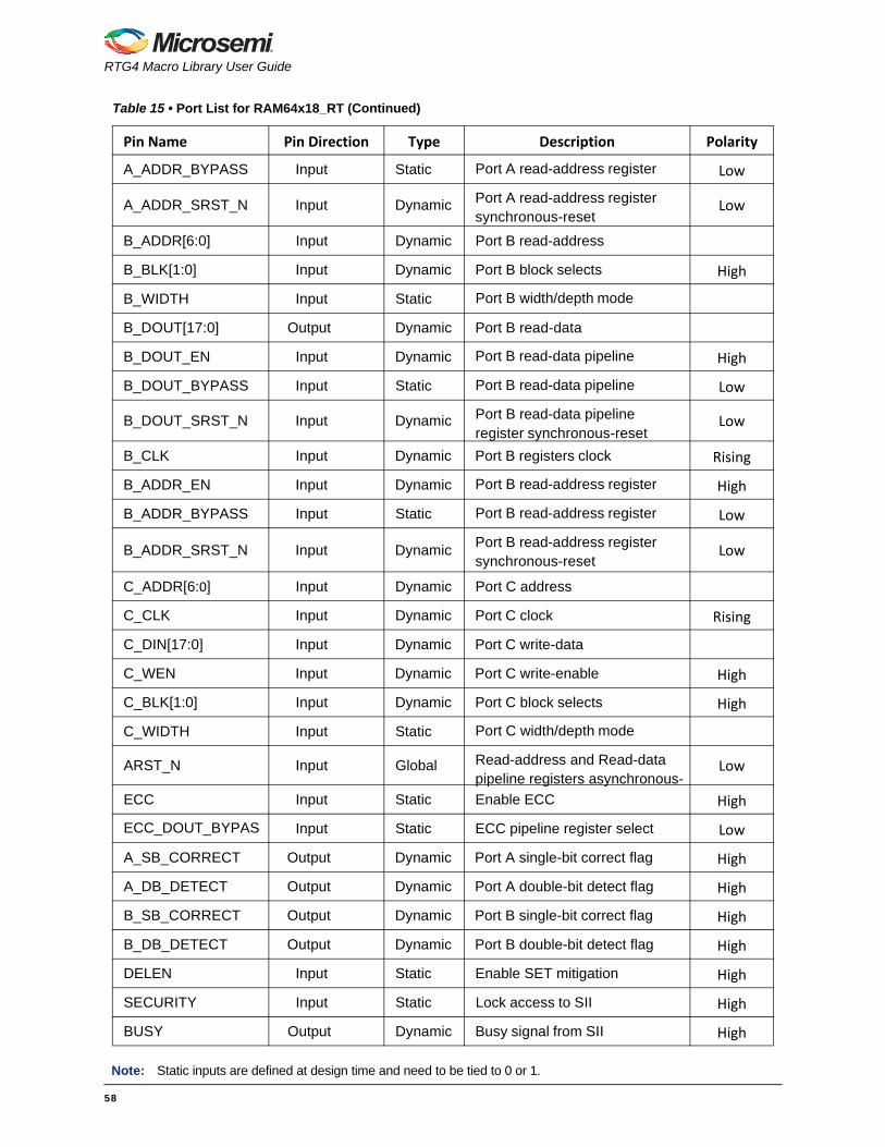
Table 15 • Port List for RAM64x18_RT
Pin Name Pin Direction Type Description Polarity
A_ADDR[6:0] Input Dynamic Port A read-address
A_BLK[1:0] Input Dynamic Port A block selects High
A_WIDTH Input Static Port A width/depth mode
A_DOUT[17:0] Output Dynamic Port A read-data
A_DOUT_EN Input Dynamic Port A read-data pipeline High
A_DOUT_BYPASS Input Static Port A read-data pipeline Low
A_DOUT_SRST_N Input Dynamic Port A read-data pipeline register synchronous-reset
Low
A_CLK Input Dynamic Port A registers clock Rising
A_ADDR_EN Input Dynamic Port A read-address register High
57
RTG4 Macro Library User Guide
Note: Static inputs are defined at design time and need to be tied to 0 or 1.
Pin Name Pin Direction Type Description Polarity
A_ADDR_BYPASS Input Static Port A read-address register Low
A_ADDR_SRST_N Input Dynamic Port A read-address register synchronous-reset
Low
B_ADDR[6:0] Input Dynamic Port B read-address
B_BLK[1:0] Input Dynamic Port B block selects High
B_WIDTH Input Static Port B width/depth mode
B_DOUT[17:0] Output Dynamic Port B read-data
B_DOUT_EN Input Dynamic Port B read-data pipeline High
B_DOUT_BYPASS Input Static Port B read-data pipeline Low
B_DOUT_SRST_N Input Dynamic Port B read-data pipeline register synchronous-reset
Low
B_CLK Input Dynamic Port B registers clock Rising
B_ADDR_EN Input Dynamic Port B read-address register High
B_ADDR_BYPASS Input Static Port B read-address register Low
B_ADDR_SRST_N Input Dynamic Port B read-address register synchronous-reset
Low
C_ADDR[6:0] Input Dynamic Port C address
C_CLK Input Dynamic Port C clock Rising
C_DIN[17:0] Input Dynamic Port C write-data
C_WEN Input Dynamic Port C write-enable High
C_BLK[1:0] Input Dynamic Port C block selects High
C_WIDTH Input Static Port C width/depth mode
ARST_N Input Global Read-address and Read-data pipeline registers asynchronous-
Low
ECC Input Static Enable ECC High
ECC_DOUT_BYPAS Input Static ECC pipeline register select Low
A_SB_CORRECT Output Dynamic Port A single-bit correct flag High
A_DB_DETECT Output Dynamic Port A double-bit detect flag High
B_SB_CORRECT Output Dynamic Port B single-bit correct flag High
B_DB_DETECT Output Dynamic Port B double-bit detect flag High
DELEN Input Static Enable SET mitigation High
SECURITY Input Static Lock access to SII High
BUSY Output Dynamic Busy signal from SII High
Table 15 • Port List for RAM64x18_RT (Continued)
58

RTG4 Macro Library User Guide
Port Description
A_WIDTH, B_WIDTH and C_WIDTHTable 16 lists the width/depth mode selections for each port.
C_WENThis is the write-enable signal for port C.
A_ADDR, B_ADDR and C_ADDRTable 17 lists the address buses for each port. 7 bits are required to address 128 independent locations in x9 mode. In wider modes, fewer address bits are used. The required bits are MSB justified and unused LSB bits must be tied to 0.
C_DINTable 18 lists the write-data input for port C. The required bits are LSB justified and unused MSB bits must be tied to 0.
Table 16 • Width/Depth Mode Selection
Depth x Width A_WIDTH/B_WIDTH/C_WIDTH
128x9, 128x12 0
64x16, 64x18 1
Table 17 • Address Buses Used and Unused Bits
Depth x Width
A_ADDR/B_ADDR/C_ADDR
Used BitsUnused Bits
(must be tied to zero)
128x9, [6:0] None
64x18 [6:1] [0]
Table 18 • Data Input Bus Used and Unused Bits
Depth x Width
C_DIN
Used BitsUnused Bits
(must be tied to 0)
128x9 [8:0] [17:9]
128x12 [11:0] [17:12]
64x18 [17:0] None
59

RTG4 Macro Library User Guide
A_DOUT and B_DOUTTable 19 lists the read-data output buses for ports A and B. The required bits are LSB justified.
A_BLK, B_BLK and C_BLKTable 20 lists the block-port select control signals for the ports.
C_CLKAll signals on port C are synchronous to this clock signal. All write-address, write-data, C block-port select and write-enable inputs must be set up before the rising edge of the clock. The write operation begins with the rising edge.
Read-address and Read-data Pipeline Register Control signalsA_DOUT_BYPASS, A_ADDR_BYPASS, B_DOUT_BYPASS and B_ADDR_BYPASS
A_DOUT_EN, A_ADDR_EN, B_DOUT_EN and B_ADDR_EN
A_DOUT_SRST_N, A_ADDR_SRST_N, B_DOUT_SRST_N and B_ADDR_SRST_N
Table 19 • Data Output Used and Unused Bits
Depth x WidthA_DOUT/B_DOUT
Used Bits Unused Bits
128x9 [8:0] [17:9]
128x12 [11:0] [17:12]
64x18 [17:0] None
Table 20 • Block-port Select
Block-port SelectSignal
Value Result
A_BLK[1:0]Any one bit is 0 Port A is not selected and its read-data will be
forced to zero.
11 Perform read operation from port A.
B_BLK[1:0]Any one bit is 0 Port B is not selected and its read-data will be
forced to zero.
11 Perform read operation from port B.
C_BLK[1:0]Any one bit is 0 Port C is not selected.
11 Perform write operation to port C.
60

RTG4 Macro Library User Guide
Table 21 describes the functionality of the control signals on the A_ADDR, B_ADDR, A_DOUT and B_DOUT registers.
ARST_NConnects the read-address and read-data pipeline registers to the global Asynchronous-reset signal.
ECC and ECC_DOUT_BYPASSControls ECC operation.
• ECC = 0: Disable ECC.
• ECC = 1, ECC_DOUT_BYPASS = 0: Enable ECC Pipelined.
– ECC Pipelined mode inserts an additional clock cycle to Read-data.
• ECC = 1, ECC_DOUT_BYPASS = 1: Enable ECC Non-pipelined.
A_SB_CORRECT and B_SB_CORRECTOutput flag indicates single-bit correction was performed on the corresponding port.
A_DB_DETECT and B_DB_DETECTOutput flag indicates double-bit detection was performed on the corresponding port.
DELENEnable Single-event Transient mitigation.
SECURITYControl signal, when 1 locks the entire RAM64x18_RT memory from being accessed by the SII.
BUSYThis output indicates that the RAM64x18_RT memory is being accessed by the SII.
Table 21 • Truth Table for A_ADDR, B_ADDR, A_DOUT and B_DOUT Registers
ARST_N _BYPASS _CLK _EN _SRST_N D Qn+1
0 X X X X X 0
1 0 Not rising X X X Qn
1 0 ↑ 0 X X Qn
1 0 ↑ 1 0 X 0
1 0 ↑ 1 1 D D
1 1 X X X D D
61

RTG4 Macro Library User Guide
MACC18 bit x 18 bit multiply-accumulate MACC block
The MACC block can accumulate the current multiplication product with a previous result, a constant, a dynamic value, or a result from another MACC block. Each MACC block can also be configured to perform a Dot-product operation. All the signals of the MACC block (except CDIN and CDOUT) have optional registers.
Figure 60 • MACC Ports
62

RTG4 Macro Library User Guide
Table 22 • Ports
Port Name Direction Type Polarity Description
DOTP Input Static High
Dot-product mode. When DOTP = 1, MACC block performs Dot-product of two pairs of 9-bit operands.When DOTP = 0, it is called the normal mode.
SIMD Input Static Reserved. Must be 0.
CLK[1:0] Input Dynamic Rising edge
Input clocks. • CLK[1] is the clock for A[17:9], B[17:9],
C[43:18], P[43:18], OVFL_CARRYOUT, ARSHFT17, CDSEL, FDBKSEL and SUB registers.
• CLK[0] is the clock for A[8:0], B[8:0], C[17:0], CARRYIN and P[17:0].
In normal mode, ensure CLK[1] = CLK[0].
A[17:0] Input Dynamic High Input data A.
A_BYPASS[1:0] Input Static High
Bypass data A registers. • A_BYPASS[1] is for A[17:9]. Connect to 1,
if not registered.
• A_BYPASS[0] is for A[8:0]. Connect to 1, if not registered.
In normal mode, ensure A_BYPASS[0] = A_BYPASS[1].
A_ARST_N[1:0] Input Dynamic Low
Asynchronous reset for data A registers.Connect both A_ARST_N[1] and = A_ARST_N[0] to 1 or to the global Asynchronous reset of the design
A_SRST_N[1:0] Input Dynamic Low
Synchronous reset for data A registers.• A_SRST_N[1] is for A[17:9]. Connect to 1,
if not registered.
• A_SRST_N[0] is for A[8:0]. Connect to 1, if not registered.
In normal mode, ensure A_SRST_N[1] = A_SRST_N[0].
A_EN[1:0] Input Dynamic High
Enable for data A registers. • A_EN[1] is for A[17:9]. Connect to 1, if not
registered.
• A_EN[0] is for A[8:0]. Connect to 1, if not registered.
In normal mode, ensure A_EN[1] = A_EN[0].
63

RTG4 Macro Library User Guide
B[17:0] Input Dynamic High Input data B.
B_BYPASS[1:0] Input Static High
Bypass data B registers. • B_BYPASS[1] is for B[17:9]. Connect to 1,
if not registered.
• B_BYPASS[0] is for B[8:0]. Connect to 1, if not registered.
In normal mode, ensure B_BYPASS[0] = B_BYPASS[1].
B_ARST_N[1:0] Input Dynamic Low
Asynchronous reset for data B registers. In normal mode, ensure • Connect both B_ARST_N[1] and
B_ARST_N[0] to 1 or to the global Asynchronous reset of the design.
B_SRST_N[1:0] Input Dynamic Low
Synchronous reset for data B registers.• B_SRST_N[1] is for B[17:9]. Connect to 1,
if not registered.
• B_SRST_N[0] is for B[8:0]. Connect to 1, if not registered.
In normal mode, ensure B_SRST_N[1] = B_SRST_N[0].
B_EN[1:0] Input Dynamic High
Enable for data B registers. • B_EN[1] is for B[17:9]. Connect to 1, if not
registered.
• B_EN[0] is for B[8:0]. Connect to 1, if not registered.
In normal mode, ensure B_EN[1] = B_EN[0].
P[43:0] Output High
Result data. Normal mode • P = D + (CARRYIN + C) + (A * B), when
SUB = 0
• P = D + (CARRYIN + C) - (A * B), when SUB = 1
Dot-product mode • P = D + (CARRYIN + C) + 512 * ((AL * BH)
+ (AH * BL)), when SUB = 0
• P = D + (CARRYIN + C) - 512 * ((AL * BH) + (AH * BL)), when SUB = 1
Notation: • AL = A[8:0], AH = A[17:9]
• BL = B[8:0], BH = B[17:9]
Refer to Table 25 on page 70 to see how operand D is obtained from P, CDIN or 0.
Table 22 • Ports (Continued)
Port Name Direction Type Polarity Description
64

RTG4 Macro Library User Guide
OVFL_CARRYOUT Output High
Overflow or CarryOut • Overflow when OVFL_CARRYOUT_SEL =
0 OVFL_CARRYOUT = (SUM[45] ^ SUM[44]) | (SUM[44] ^ SUM[43])
• CarryOut when OVFL_CARRYOUT_SEL = 1 OVFL_CARRYOUT = C[43] ^ D[43] ^ SUM[44]
P_BYPASS[1:0] Input Static High
Bypass result P registers. • P_BYPASS[1] is for P[43:18] and
OVFL_CARRYOUT. Connect to 1, if not registered.
• P_BYPASS[0] is for P[17:0]. Connect to 1, if not registered.
In normal mode, ensure P_BYPASS[0] = P_BYPASS[1].
P_ARST_N[1:0] Input Dynamic Low
Asynchronous reset for result P registers. Connect both P_ARST_N[1] and P_ARST_N[0] to 1 or to the global Asynchronous reset of the design
P_SRST_N[1:0] Input Dynamic Low
Synchronous reset for result P registers. • P_SRST_N[1] is for P[43:18] and
OVFL_CARRYOUT. Connect to 1, if not registered.
• P_SRST_N[0] is for P[17:0]. Connect to 1, if not registered.
In normal mode, ensure P_SRST_N[1] = P_SRST_N[0].
P_EN[1:0] Input Dynamic High
Enable for result P registers. • P_EN[1] is for P[43:18] and
OVFL_CARRYOUT. Connect to 1, if not registered.
• P_EN[0] is for P[17:0]. Connect to 1, if not registered.
In normal mode, ensure P_EN[1] = P_EN[0].
CDOUT[43:0] Output Cascade High
Cascade output of result P. CDOUT is the same as P. The entire bus must either be dangling or drive an entire CDIN of another MACC block in cascaded mode.
CARRYIN Input Dynamic High CarryIn for operand C.
Table 22 • Ports (Continued)
Port Name Direction Type Polarity Description
65
RTG4 Macro Library User Guide
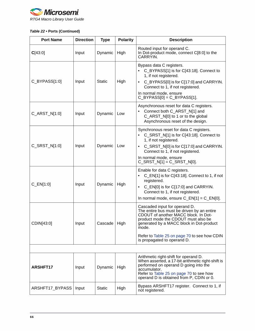
C[43:0] Input Dynamic HighRouted input for operand C. In Dot-product mode, connect C[8:0] to the CARRYIN.
C_BYPASS[1:0] Input Static High
Bypass data C registers.• C_BYPASS[1] is for C[43:18]. Connect to
1, if not registered.
• C_BYPASS[0] is for C[17:0] and CARRYIN. Connect to 1, if not registered.
In normal mode, ensure C_BYPASS[0] = C_BYPASS[1].
C_ARST_N[1:0] Input Dynamic Low
Asynchronous reset for data C registers. • Connect both C_ARST_N[1] and
C_ARST_N[0] to 1 or to the global Asynchronous reset of the design.
C_SRST_N[1:0] Input Dynamic Low
Synchronous reset for data C registers. • C_SRST_N[1] is for C[43:18]. Connect to
1, if not registered.
• C_SRST_N[0] is for C[17:0] and CARRYIN. Connect to 1, if not registered.
In normal mode, ensure C_SRST_N[1] = C_SRST_N[0].
C_EN[1:0] Input Dynamic High
Enable for data C registers. • C_EN[1] is for C[43:18]. Connect to 1, if not
registered.
• C_EN[0] is for C[17:0] and CARRYIN. Connect to 1, if not registered.
In normal mode, ensure C_EN[1] = C_EN[0].
CDIN[43:0] Input Cascade High
Cascaded input for operand D. The entire bus must be driven by an entire CDOUT of another MACC block. In Dot-product mode the CDOUT must also be generated by a MACC block in Dot-product mode.
Refer to Table 25 on page 70 to see how CDIN is propagated to operand D.
ARSHFT17 Input Dynamic High
Arithmetic right-shift for operand D. When asserted, a 17-bit arithmetic right-shift is performed on operand D going into the accumulator. Refer to Table 25 on page 70 to see how operand D is obtained from P, CDIN or 0.
ARSHFT17_BYPASS Input Static High Bypass ARSHFT17 register. Connect to 1, if not registered.
Table 22 • Ports (Continued)
Port Name Direction Type Polarity Description
66
RTG4 Macro Library User Guide
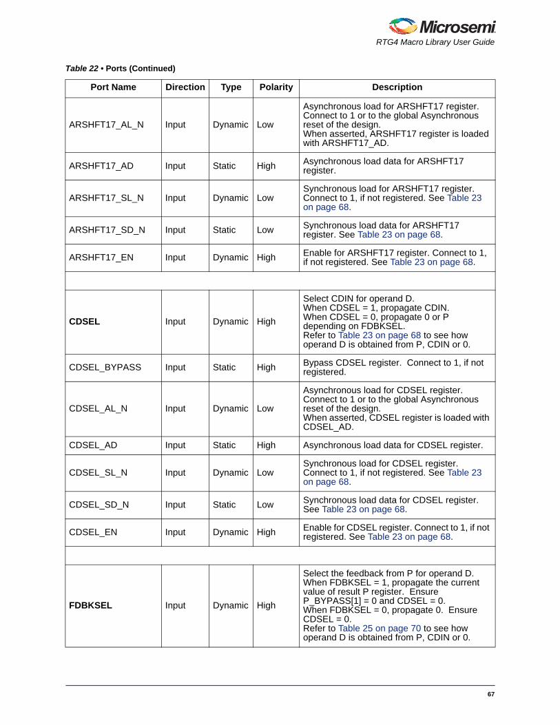
ARSHFT17_AL_N Input Dynamic Low
Asynchronous load for ARSHFT17 register.Connect to 1 or to the global Asynchronous reset of the design.When asserted, ARSHFT17 register is loaded with ARSHFT17_AD.
ARSHFT17_AD Input Static High Asynchronous load data for ARSHFT17 register.
ARSHFT17_SL_N Input Dynamic LowSynchronous load for ARSHFT17 register. Connect to 1, if not registered. See Table 23 on page 68.
ARSHFT17_SD_N Input Static Low Synchronous load data for ARSHFT17 register. See Table 23 on page 68.
ARSHFT17_EN Input Dynamic High Enable for ARSHFT17 register. Connect to 1, if not registered. See Table 23 on page 68.
CDSEL Input Dynamic High
Select CDIN for operand D. When CDSEL = 1, propagate CDIN. When CDSEL = 0, propagate 0 or P depending on FDBKSEL. Refer to Table 23 on page 68 to see how operand D is obtained from P, CDIN or 0.
CDSEL_BYPASS Input Static High Bypass CDSEL register. Connect to 1, if not registered.
CDSEL_AL_N Input Dynamic Low
Asynchronous load for CDSEL register. Connect to 1 or to the global Asynchronous reset of the design.When asserted, CDSEL register is loaded with CDSEL_AD.
CDSEL_AD Input Static High Asynchronous load data for CDSEL register.
CDSEL_SL_N Input Dynamic LowSynchronous load for CDSEL register. Connect to 1, if not registered. See Table 23 on page 68.
CDSEL_SD_N Input Static Low Synchronous load data for CDSEL register. See Table 23 on page 68.
CDSEL_EN Input Dynamic High Enable for CDSEL register. Connect to 1, if not registered. See Table 23 on page 68.
FDBKSEL Input Dynamic High
Select the feedback from P for operand D.When FDBKSEL = 1, propagate the current value of result P register. Ensure P_BYPASS[1] = 0 and CDSEL = 0. When FDBKSEL = 0, propagate 0. Ensure CDSEL = 0. Refer to Table 25 on page 70 to see how operand D is obtained from P, CDIN or 0.
Table 22 • Ports (Continued)
Port Name Direction Type Polarity Description
67

RTG4 Macro Library User Guide
FDBKSEL_BYPASS Input Static High Bypass FDBKSEL register. Connect to 1, if not registered.
FDBKSEL_AL_N Input Dynamic Low
Asynchronous load for FDBKSEL register. Connect to 1 or to the global Asynchronous reset of the design. When asserted, FDBKSEL register is loaded with FDBKSEL_AD.
FDBKSEL_AD Input Static High Asynchronous load data for FDBKSEL register.
FDBKSEL_SL_N Input Dynamic LowSynchronous load for FDBKSEL register. Connect to 1, if not registered. See Table 23 on page 68.
FDBKSEL_SD_N Input Static Low Synchronous load data for FDBKSEL register. See Table 23 on page 68.
FDBKSEL_EN Input Dynamic High Enable for FDBKSEL register. Connect to 1, if not registered. See Table 23 on page 68.
SUB Input Dynamic High Subtract operation.
SUB_BYPASS Input Static High Bypass SUB register. Connect to 1, if not registered.
SUB_AL_N Input Dynamic Low
Asynchronous load for SUB register. Connect to 1 or to the global Asynchronous reset of the design. When asserted, SUB register is loaded with SUB_AD.
SUB_AD Input Static High Asynchronous load data for SUB register.
SUB_SL_N Input Dynamic Low Synchronous load for SUB register. Connect to 1, if not registered. See Table 23.
SUB_SD_N Input Static Low Synchronous load data for SUB register. See Table 23.
SUB_EN Input Dynamic High Enable for SUB register. Connect to 1, if not registered. See Table 23.
Table 23 • Truth Table for Control Registers ARSHFT17, CDSEL, FDBKSEL and SUB
_AL_N _AD _BYPASS _CLK _EN _SL_N _SD_N D Qn+1
0 AD X X X X X X AD
1 X 0 Not rising X X X X Qn
1 X 0 0 X X X Qn
1 X 0 1 0 SDn X !SDn
Table 22 • Ports (Continued)
Port Name Direction Type Polarity Description
68

RTG4 Macro Library User Guide
1 X 0 1 1 X D D
1 X 1 X 0 X X X Qn
1 X 1 X 1 0 SDn X !SDn
1 X 1 X 1 1 X D D
Table 23 • Truth Table for Control Registers ARSHFT17, CDSEL, FDBKSEL and SUB (Continued)
_AL_N _AD _BYPASS _CLK _EN _SL_N _SD_N D Qn+1
69

RTG4 Macro Library User Guide
Table 24 • Truth Table - Data Registers A, B, C, CARRYIN, P and OVFL_CARRYOUT
_ARST_N _BYPASS _CLK _EN _SRST_N D Qn+1
0 X X X X X 0
1 0 Not rising X X X Qn
1 0 0 X X Qn
1 0 1 0 X 0
1 0 1 1 D D
1 1 X 0 X X Qn
1 1 X 1 0 X 0
1 1 X 1 1 D D
Table 25 • Truth Table - Propagating Data to Operand D
FDBKSEL CDSEL ARSHFT17 Operand D
0 0 x 44'b0
x 1 0 CDIN[43:0]
x 1 1 17CDIN[43],CDIN[43:17]
1 0 0 P[43:0]
1 0 1 17P[43],P[43:17]
70

A – Product Support
Microsemi SoC Products Group backs its products with various support services, including Customer Service, Customer Technical Support Center, a website, electronic mail, and worldwide sales offices. This appendix contains information about contacting Microsemi SoC Products Group and using these support services.
Customer ServiceContact Customer Service for non-technical product support, such as product pricing, product upgrades, update information, order status, and authorization.
From North America, call 800.262.1060From the rest of the world, call 650.318.4460Fax, from anywhere in the world, 650.318.8044
Customer Technical Support CenterMicrosemi SoC Products Group staffs its Customer Technical Support Center with highly skilled engineers who can help answer your hardware, software, and design questions about Microsemi SoC Products. The Customer Technical Support Center spends a great deal of time creating application notes, answers to common design cycle questions, documentation of known issues, and various FAQs. So, before you contact us, please visit our online resources. It is very likely we have already answered your questions.
Technical SupportFor Microsemi SoC Products Support, visit http://www.microsemi.com/products/fpga-soc/design-support/fpga-soc-support.
WebsiteYou can browse a variety of technical and non-technical information on the Microsemi SoC Products Group home page, at www.microsemi.com/soc.
Contacting the Customer Technical Support CenterHighly skilled engineers staff the Technical Support Center. The Technical Support Center can be contacted by email or through the Microsemi SoC Products Group website.
EmailYou can communicate your technical questions to our email address and receive answers back by email, fax, or phone. Also, if you have design problems, you can email your design files to receive assistance. We constantly monitor the email account throughout the day. When sending your request to us, please be sure to include your full name, company name, and your contact information for efficient processing of your request.
The technical support email address is [email protected].
71
MOCA
WOSaFa
E-
©2reloCosere
Microsemi makes no warranty, representation, or guarantee regarding the information contained herein orthe suitability of its products and services for any particular purpose, nor does Microsemi assume anyliability whatsoever arising out of the application or use of any product or circuit. The products soldhereunder and any other products sold by Microsemi have been subject to limited testing and should notbe used in conjunction with mission-critical equipment or applications. Any performance specifications arebelieved to be reliable but are not verified, and Buyer must conduct and complete all performance andother testing of the products, alone and together with, or installed in, any end-products. Buyer shall not relyon any data and performance specifications or parameters provided by Microsemi. It is the Buyer'sresponsibility to independently determine suitability of any products and to test and verify the same. Theinformation provided by Microsemi hereunder is provided "as is, where is" and with all faults, and the entirerisk associated with such information is entirely with the Buyer. Microsemi does not grant, explicitly orimplicitly, to any party any patent rights, licenses, or any other IP rights, whether with regard to such
About Microsemi
Microsemi Corporation (Nasdaq: MSCC) offers a comprehensive portfolio of semiconductorand system solutions for communications, defense & security, aerospace and industrialmarkets. Products include high-performance and radiation-hardened analog mixed-signalintegrated circuits, FPGAs, SoCs and ASICs; power management products; timing andsynchronization devices and precise time solutions, setting the world's standard for time; voiceprocessing devices; RF solutions; discrete components; Enterprise Storage andCommunication solutions, security technologies and scalable anti-tamper products; Ethernetsolutions; Power-over-Ethernet ICs and midspans; as well as custom design capabilities andservices. Microsemi is headquartered in Aliso Viejo, Calif. and has approximately 4,800employees globally. Learn more at www.microsemi.com.icrosemi Corporate Headquarters
ne Enterprise, Aliso Viejo, 92656 USA
ithin the USA: +1 (800) 713-4113 utside the USA: +1 (949) 380-6100les: +1 (949) 380-6136 x: +1 (949) 215-4996
mail: [email protected]
016 Microsemi Corporation. All rights served. Microsemi and the Microsemi go are trademarks of Microsemi rporation. All other trademarks and
My CasesMicrosemi SoC Products Group customers may submit and track technical cases online by going to My Cases.
Outside the U.S.Customers needing assistance outside the US time zones can either contact technical support via email ([email protected]) or contact a local sales office.
Visit About Us for sales office listings and corporate contacts.
Sales office listings can be found at www.microsemi.com/soc/company/contact/default.aspx.
ITAR Technical SupportFor technical support on RH and RT FPGAs that are regulated by International Traffic in Arms Regulations (ITAR), contact us via [email protected]. Alternatively, within My Cases, select Yes in the ITAR drop-down list. For a complete list of ITAR-regulated Microsemi FPGAs, visit the ITAR web page.
5-02-00613-4/06.16
information itself or anything described by such information. Information provided in this document isproprietary to Microsemi, and Microsemi reserves the right to make any changes to the information in thisdocument or to any products and services at any time without notice.
rvice marks are the property of their spective owners.