ron mancini and charles wray texas instruments · 1-3 analog electronics in a day analog electronic...
TRANSCRIPT

1-1
Analog Electronics In A DayAnalog Electronic Design
1-1
fast forwardfast forward
This presentation is brought to you by . . .
This presentation is brought to you by . . .
Look here on slides for additional details starting at slide 1-14.

1-2
Analog Electronics In A DayAnalog Electronic Design
1-2
Ron Mancini and Charles WrayTexas Instruments
Look here on slides for additional details starting at slide 1-14.

1-3
Analog Electronics In A DayAnalog Electronic Design
1-3
Teach the non-analog person enough analog theory to enable
them to use and understand application notes.

1-4
Analog Electronics In A DayAnalog Electronic Design
1-4
When a job comes into the house, if the digital guys can’t do it, it’s
analog.

1-5
Analog Electronics In A DayAnalog Electronic Design
1-5
Analog design couples the art and science of electronics into one
entity.

1-6
Analog Electronics In A DayAnalog Electronic Design
1-6
• Passive devices• Active devices• Circuit equations• Derivation of the ideal op amp equation• Feedback analysis tools• Stability• Voltage feedback op amp compensation

1-7
Analog Electronics In A DayAnalog Electronic Design
1-7
• Current feedback op amp analysis• Circuit board layout• Non-ideal op amp conditions• High speed amplifier applications• Single-supply op amp applications• Converter basics• Converter Applications• Power applications

1-8
Analog Electronics In A DayAnalog Electronic Design
1-8
1. Introduction 1-1• Why are we here• What you will learn• Review outline
2. Passive Devices 2-1• Resistors• Capacitors• Inductors• Diodes
3. Active Devices 3-1• Ideal and first level real
models BJT, JFET, MOSFET, VFB op amp,CFB op amp, comparator

1-9
Analog Electronics In A DayAnalog Electronic Design
1-9
4. Circuit Equations 4-1• Ohm’s law• Kirchoff’s laws • Voltage divider rule• Current divider rule• Thevenin’s rule• Norton’s rule• Superposition
5. Derivation of ideal op amp equation 5-1• Use voltage divider law,
Kirchoff’s law and Ohm’slaw
• Do inverting, non-inverting, differential, groundedcomponent in feedback loop

1-10
Analog Electronics In A DayAnalog Electronic Design
1-10
6. Feedback Analysis Tools 6-1• Block diagrams • Bode plots
7. Stability 7-1• Stability equation• VFB op amp equations• Second order equations• Overshoot and stability• Phase margin• Oscillation and Oscillators
8. VFB Op Amp Compensation 8-1• Dominant pole• Feed forward• Lead/lag• Compensated attenuator

1-11
Analog Electronics In A DayAnalog Electronic Design
1-11
9. CFB Op Amp Analysis 9-1• Derive the equations• Stability Analysis
10. Circuit Board Layout 10-1• Ground Plane• Decoupling capacitors• Parallel traces• Faraday shield• Capacitance• Differential versus single-ended
11. Non-Ideal Conditions 11-1• Offset voltage• Error versus frequency• Common-mode rejection versus frequency• Output swing-versus frequency, load, and
distortion• Noise

1-12
Analog Electronics In A DayAnalog Electronic Design
1-12
12. Single-Supply Op Amp Applications 12-1• Biasing calculations • Computer calculations
13. Circuits High Speed Amplifier Applications 13-1• Communications circuits • Imaging circuits • Video/multimedia circuits • Instrumentation circuits
14. Converter Basics 14-1• Digital math• Basic DAC theory and configurations• Basic ADC theory and configurations• Error definitions and curves

1-13
Analog Electronics In A DayAnalog Electronic Design
1-13
15. Converter Applications 15-1• Communications circuits• FIFO circuits• ATS systems circuits• WLL circuits• Low frequency applications circuits
16. Power Applications 16-1• LDO circuits • Power distribution circuits • DSP power supplies• DC/DC converters• Battery management circuits

1-14
Analog Electronics In A DayAnalog Electronic Design
1-14
• Feedback ensures that circuit performance is determined by passive, not active, devices.
• Passive device accuracy and stability is paramount when they control circuit performance.
Passive devices are the resistors, capacitors, and inductors required to build electronic hardware, but they always have a gain less than one. Passives can multiply a signal by values less than one, as is shown in section four, but they can’t multiply by more than one because of their lack of gain. All the glory goes to the sophisticated high gain amplifiers, but they are useless without the resistors and capacitors which control their gain. Good circuit design practice demands accurate and stable amplifiers, but the active devices are by nature unstable, so they are tamed with passives. Feedback is employed in almost all circuit designs to insure that the circuit performance is a function of the passive rather than the active components.
Passive devices are neglected in the rush to complete the design of an electronic system. Many engineers select passive devices as an after thought; they just pick them from a list of standard components. Although this practice is adequate for some circuits, it does not suffice in the demanding world of high frequency amplifiers, precision sample-holds, data converters, or other demanding circuits. The hardware designer must select adequate passives for demanding applications.

1-15
Analog Electronics In A DayAnalog Electronic Design
1-15
• Accuracy and stability• Passive devices must be:
– Inexpensive– Small– Surface mountable
The selection criteria for passive devices is very demanding. The first selection criterion for passives is that they must be accurate and stable to insure proper circuit performance. After this criterion is satisfied, there are requirements for low cost, small size and surface mounting. Accuracy normally dictates larger size, so the accuracy and small size requirements often conflict. More new surface mount components are coming out each day; thus it is a constant search to find accurate and stable passives which meet all the criteria.
1-16
Analog Electronics In A DayAnalog Electronic Design
1-16
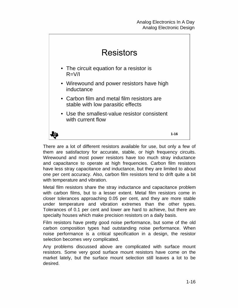
• The circuit equation for a resistor isR=V/I
• Wirewound and power resistors have high inductance
• Carbon film and metal film resistors are stable with low parasitic effects
• Use the smallest-value resistor consistent with current flow
There are a lot of different resistors available for use, but only a few of them are satisfactory for accurate, stable, or high frequency circuits. Wirewound and most power resistors have too much stray inductance and capacitance to operate at high frequencies. Carbon film resistors have less stray capacitance and inductance, but they are limited to about one per cent accuracy. Also, carbon film resistors tend to drift quite a bit with temperature and vibration.
Metal film resistors share the stray inductance and capacitance problem with carbon films, but to a lesser extent. Metal film resistors come in closer tolerances approaching 0.05 per cent, and they are more stable under temperature and vibration extremes than the other types. Tolerances of 0.1 per cent and lower are hard to achieve, but there are specialty houses which make precision resistors on a daily basis.
Film resistors have pretty good noise performance, but some of the old carbon composition types had outstanding noise performance. Whennoise performance is a critical specification in a design, the resistor selection becomes very complicated.
Any problems discussed above are complicated with surface mount resistors. Some very good surface mount resistors have come on the market lately, but the surface mount selection still leaves a lot to be desired.

1-17
Analog Electronics In A DayAnalog Electronic Design
1-17
Ideal ResistorR
CG
LL LL
CP
R/2 R/2
Inexperienced engineers assume that a resistor is just a resistor, and it really is a very complicated circuit. LL simulates the inductance of each lead. CP is the capacitance across the resistor, thus it appears to be in parallel with the resistor. CP is about 0.5 pF for a 250 mW resistor.
CG is formed by the resistor body and the ground plane, and it, like the rest of these stray effects, is really a distributed effect. Because it is small it appears as a capacitor connected to ground from the center of the resistor. Depending on the physical size of the resistor, CP ranges from 0.01 pF on up to 0.5 pF.
The stray effects are reduced as the size of the resistor is reduced. Surface mount resistors have the best high frequency performanceprimarily because of their small size.

1-18
Analog Electronics In A DayAnalog Electronic Design
1-18
• Potentiometers are:– Variable resistors– Used to adjust the voltage or current in the
circuit• Potentiometers have:
– All the problems associated with fixed resistors
– Severe drift problems caused by temperature and vibration
Potentiometers or pots are used to adjust the voltage or current at some point in a circuit. When tolerances stack up or when the specifications for a component can’t be predicted accurately, pots are used to adjust out the tolerances thus obtaining the correct circuit parameter. The overuse of potentiometers is often a sign of poor design, but some equipment such as projection displays require many adjustments.
Pots have all of the bad problems associated with fixed resistors, and they exacerbate some of them and introduce new one. Pots are notorious for drifting under temperature or vibration stress. The connection from the resistive element to the lead is critical in fixed resistor design, and it is so good that it isn’t considered a problem except with fractional ohm resistors. The wiper on a pot must slide across the resistive element, thus a good firm connection is impossible leading to a fractional ohmconnection.
Systems that use large numbers of pots are converting to digital-to analog (DAC) converters. DACs come eight and twelve to a package, and their cost is equivalent to that of a pot. The adjustments are made through the keyboard or through a production test fixture. Smart systems self calibrate on start up thus eliminating the need for pots.

1-19
Analog Electronics In A DayAnalog Electronic Design
1-19
Used to set a reference voltage Used as a variable resistor
VOUT
VREF
IN
OUT
IN OUT
Pots are used in two major applications: voltage dividers for setting a reference and as variable resistors. The voltage divider application requires that the load be much higher in impedance than the pot to prevent loading of the pot by the load. This is a very popular application for pots, and the reference input voltage must be very stable because the circuit follows the reference. The reference voltage source should by well decoupled with a good grade capacitor to localize noise and keep it from spreading to other circuits.
Variable resistor applications can be very subtle, but the first thing to remember is that the pot has a limited current carrying capability. Do not connect the variable resistor configuration between the power supply and ground even if it connects through a semiconductor junction. When the variable resistor configuration is connected to ground in some manner, a series resistor must be inserted in the circuit to limit the current flow to a safe value.
1-20
Analog Electronics In A DayAnalog Electronic Design
1-20
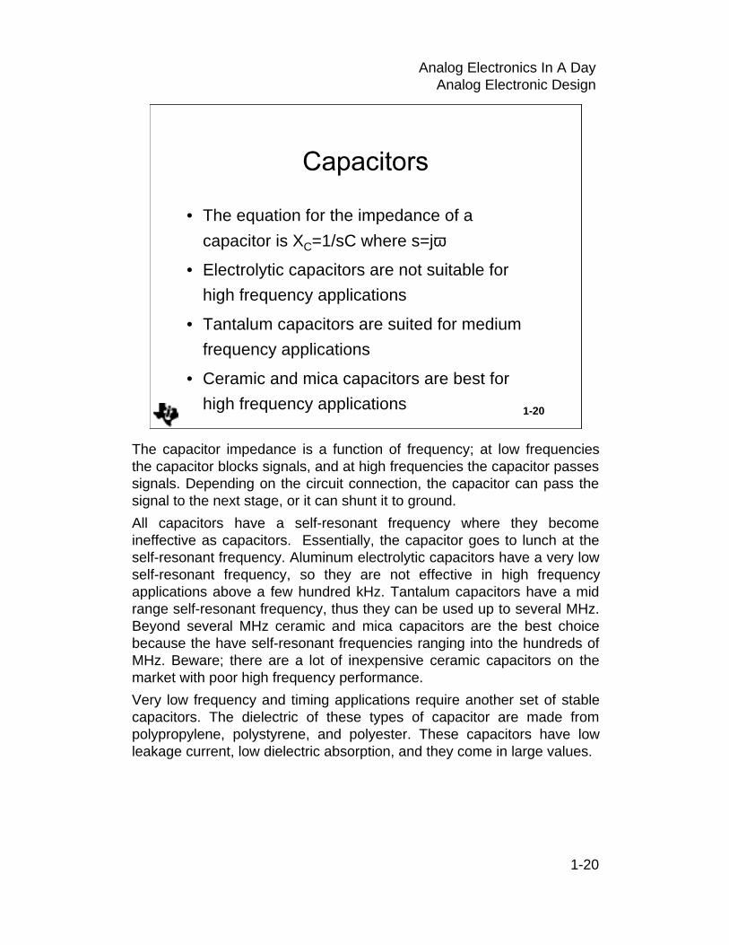
• The equation for the impedance of a
capacitor is XC=1/sC where s=jω
• Electrolytic capacitors are not suitable for
high frequency applications
• Tantalum capacitors are suited for medium
frequency applications
• Ceramic and mica capacitors are best for
high frequency applications
The capacitor impedance is a function of frequency; at low frequencies the capacitor blocks signals, and at high frequencies the capacitor passes signals. Depending on the circuit connection, the capacitor can pass the signal to the next stage, or it can shunt it to ground.
All capacitors have a self-resonant frequency where they become ineffective as capacitors. Essentially, the capacitor goes to lunch at the self-resonant frequency. Aluminum electrolytic capacitors have a very low self-resonant frequency, so they are not effective in high frequency applications above a few hundred kHz. Tantalum capacitors have a mid range self-resonant frequency, thus they can be used up to several MHz. Beyond several MHz ceramic and mica capacitors are the best choice because the have self-resonant frequencies ranging into the hundreds of MHz. Beware; there are a lot of inexpensive ceramic capacitors on the market with poor high frequency performance.
Very low frequency and timing applications require another set of stable capacitors. The dielectric of these types of capacitor are made from polypropylene, polystyrene, and polyester. These capacitors have low leakage current, low dielectric absorption, and they come in large values.

1-21
Analog Electronics In A DayAnalog Electronic Design
1-21
L
RP
C ESR
L models the lead and internal inductance of the capacitor. Except for dielectrics such as ceramic and mica, the internal inductance is dominant at high frequencies. In high frequency capacitors the lead inductance can be approximated as 1/12 NH per foot. The combination of internal and lead inductance causes the capacitor to become self-resonant, and at frequencies above resonance the capacitor will appear to be an inductor. High frequency applications demand capacitors with high self resonant frequencies and short leads which is why surface mount capacitors are used so often in high frequency circuits design.
The actual value of the capacitor is C. ESR stands for equivalent series resistance, and ESR is the effective resistance of the capacitor at the operating frequency. It is an important parameter when high currents are involved. Power supply filter design requires low ESR because voltage is dropped across the ESR, and the current flowing through the capacitor causes power dissipation resulting self heating. ESR is not an important parameter in the design of high frequency or signal processing circuits, thus is only specified for aluminum electrolytic and tantalum capacitors.
The parallel resistance of a capacitor is modeled by RP. This resistance is a function of the operating voltage and capacitor temperature; hence, it drifts quite a bit. The electrolytic capacitors exhibit the lowest parallel resistance, and aluminum electrolytic capacitors are often modeled with a parallel current source in place of RP. Other types of capacitors have a relatively high RP ranging in the hundreds of meg ohms.

1-22
Analog Electronics In A DayAnalog Electronic Design
1-22
• The equation for the impedance of an inductor is XL=sL where s=jω.
• Inductors have poor tolerance, and they are expensive.
• Power supplies and filters use inductors.
• Inductors requiring cores are big and heavy.
• Only the high frequency or signal filter inductor is modeled.
The primary use for inductors is for filters. There are two very different types of filter inductors: the high current inductor used in power supply filters, and the low current inductors used in signal filters.
High current inductors require cores to keep the losses within acceptable limits and to achieve high performance. The cores are big and heavy, so they contribute heavily to the cost, weight, and size of the equipment. Switching power supplies require extensive inductors or transformers to control the switching noise and smooth out the output voltage waveform.
Low current inductors are used for filters in signal processing circuits. Capacitors are used where ever possible because they are less expensive and readily available, but there are a few applications that inductors excel in. An inductive/capacitive filter has sharper slopes than a resistive/capacitive filter, thus it is a more effective filter in some applications. In general, inductors are rarely seen outside power circuits.

1-23
Analog Electronics In A DayAnalog Electronic Design
1-23
L
CP
RS
The inductor model is rather simple consisting of the inductor, L, a series resistance, RS, and the parallel capacitance, CP. The series resistance impacts the performance of the inductor considerably, and great efforts are made to keep RS at a minimum, especially in power inductors. CPdoes not come into play until the signal frequencies get in the MHz range. The parallel capacitance degrades the inductor performance at high frequencies.
1-24
Analog Electronics In A DayAnalog Electronic Design
1-24
Anode Cathode
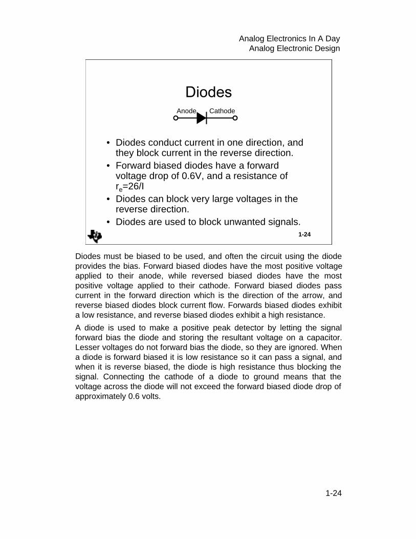
• Diodes conduct current in one direction, and they block current in the reverse direction.
• Forward biased diodes have a forward voltage drop of 0.6V, and a resistance of re=26/I
• Diodes can block very large voltages in the reverse direction.
• Diodes are used to block unwanted signals.
Diodes must be biased to be used, and often the circuit using the diode provides the bias. Forward biased diodes have the most positive voltage applied to their anode, while reversed biased diodes have the most positive voltage applied to their cathode. Forward biased diodes pass current in the forward direction which is the direction of the arrow, and reverse biased diodes block current flow. Forwards biased diodes exhibit a low resistance, and reverse biased diodes exhibit a high resistance.
A diode is used to make a positive peak detector by letting the signal forward bias the diode and storing the resultant voltage on a capacitor. Lesser voltages do not forward bias the diode, so they are ignored. When a diode is forward biased it is low resistance so it can pass a signal, and when it is reverse biased, the diode is high resistance thus blocking the signal. Connecting the cathode of a diode to ground means that the voltage across the diode will not exceed the forward biased diode drop of approximately 0.6 volts.

1-25
Analog Electronics In A DayAnalog Electronic Design
1-25
VF re
CP
IL
The forward voltage drop, VF, is shown as a battery. The forward biased diode starts with a small voltage drop, but it very quickly rises to approximately 0.6 volts for a silicon diode and 0.2 volts for a germanium diode The voltage drop is a function of the bias current, but these approximations suffice for the majority of applications.
The diode resistance, re, is also a function of the forward current, and it is approximated by the equation re = 26/I. This is an approximation of re, but it holds over a wide range of currents. When the diode is reverse biased the forward current is zero, and the equation says that re equals infinity. This is not exactly true, but the relationship is too complicated for this discussion. A simple way out of the trap is to include the current source, IL, which models a reverse biased leakage current. The leakage current is voltage and temperature sensitive, so it is best to use diodes which have very low leakage currents.
Diodes take a finite amount of time to turn on and turn off. Some of this time results from the carrier physics internal to the diode, and some of this time results from the parallel capacitance, CP. Depending on the diode and the bias conditions, CP ranges from a fraction of a pF for small switching diodes to a few hundred pF for power diodes. Remember,diodes have switching times that may have to be accounted for.

1-26
Analog Electronics In A DayAnalog Electronic Design
1-26
Active devices have gain; thus they can make up transfer functions not available to passive devices. Active devices are considerably more complicated than passive devices; thus, their models and transfer equations are more complicated than those of passive devices. Active devices are the foundation of all electronics.

1-27
Analog Electronics In A DayAnalog Electronic Design
1-27
• Comes in two flavors: NPN and PNP
• High input current
• Excellent bandwidth
• Silicon, germanium, and gallium-arsenide
• Input circuit looks like a diode
• Output circuit is high impedance
• Excellent high speed switches
The bipolar junction transistor is often shortened to BJT. The BJT was the workhorse of the semiconductor industry until the field effect transistor (FET) manufacturing process was perfected. Since then the FET has been taking sockets from the BJT, but there are many applications, such as high frequency amplifiers, where the BJT still excels. Also, the BJT manufacturing process can be simple and inexpensive, and this, coupled with the BJT’s long list of captured sockets, insures that the BJT will be around for a long time.

1-28
Analog Electronics In A DayAnalog Electronic Design
1-28
NPN
PNP
Base
Emitter
Collector
Base
Emitter
Collector
B
C
E
PNPB
C
E
NPN
BJT transistors have three areas that are doped differently to produce different transistor actions. These three areas are called the base, emitter, and collector. The base and collector are doped to have the same polarity which can be positive or negative. The BJT, like most transistors, come in two types called NPN or PNP. P stands for positive, N stands for negative, and the positive or negative regions gain their name from the doping of the semiconductor material making up the base, collector and emitter areas of the BJT.
An NPN transistor looks like two diodes with the anodes connected. The anodes connection is called the base, one cathode is the collector, and the other cathode is called the emitter. Although this illustration would not work, it does have a basis in fact because if the width of the base junction were decreased enough, the back-to-back diodes would function as a transistor. Using the back-to-back diode model, transistors are commonly checked for short circuits and open circuits with an ohmmeter. It then is no surprise that the base-emitter circuit of a BJT looks like a forward biased diode, and the base-collector looks like a reverse biased diode.

1-29
Analog Electronics In A DayAnalog Electronic Design
1-29
Collector
rCβIB=IC
Emitter
VBE IB
re
Base
The model input looks like a forward biased diode, and the inputimpedance equation is ZIN = re = IC/26. The base-emitter junction must be forward biased, thus there is a forward voltage drop of VBE. VBE is approximately 0.6 volts in a silicon transistor, and 0.2 volts in a germanium transistor. The input current is called IB.
Since the collector-base junction is reverse biased, the collector current flows from the collector to the emitter. The collector current equation is IC= β(IB) where β is the current gain of the transistor. The impedance of the collector-emitter junction is called rc, and rc is very high (in the MΩ range). Current gain and the forward voltage drop are a function of the manufacturing process, temperature, and several other items, hence they are not a stable parameter. BJT circuits which depend on β and VBE are not stable; thus, in well designed BJT circuits, the external components stabilize these parameters with feedback.
1-30
Analog Electronics In A DayAnalog Electronic Design
1-30
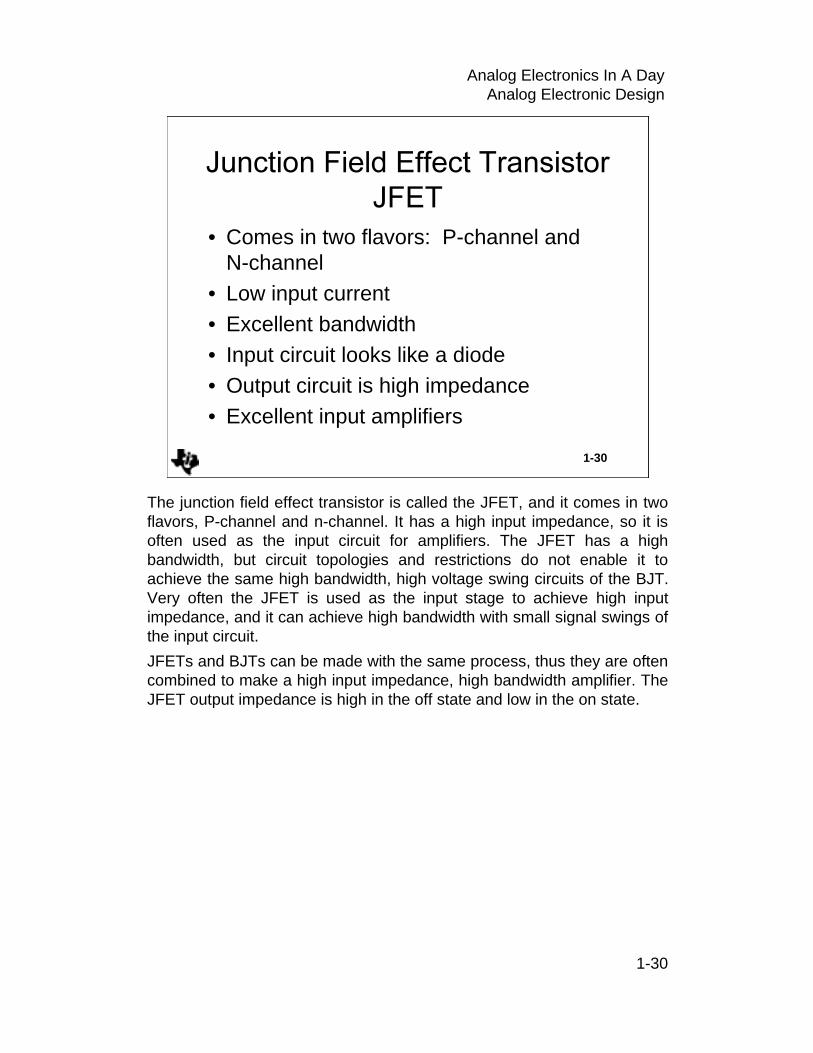
• Comes in two flavors: P-channel and N-channel
• Low input current• Excellent bandwidth• Input circuit looks like a diode• Output circuit is high impedance• Excellent input amplifiers
The junction field effect transistor is called the JFET, and it comes in two flavors, P-channel and n-channel. It has a high input impedance, so it is often used as the input circuit for amplifiers. The JFET has a high bandwidth, but circuit topologies and restrictions do not enable it to achieve the same high bandwidth, high voltage swing circuits of the BJT. Very often the JFET is used as the input stage to achieve high input impedance, and it can achieve high bandwidth with small signal swings of the input circuit.
JFETs and BJTs can be made with the same process, thus they are often combined to make a high input impedance, high bandwidth amplifier. The JFET output impedance is high in the off state and low in the on state.

1-31
Analog Electronics In A DayAnalog Electronic Design
1-31
N-Channel P-Channel
Source
Drain
Gate
Source
Drain
Gate
The JFET can be visualized as a bar of doped silicon that has a diode junction made in the middle of the bar. If the silicon bar is doped N, then the JFET is called a N-channel device. When the n-channel gate is negative with respect to the source the diode is biased off, the bar is depleted of carriers, and the source to drain resistance is quite high (several MΩ). When the n-channel gate is positive with respect to the source the diode is biased on, the bar is flooded with carriers thus causing a low source to drain resistance (as low as mΩ). The converse is true for a P-channel JFET.

1-32
Analog Electronics In A DayAnalog Electronic Design
1-32
Source
Gate
eg RO
Drain
gmeg
When the JFET is biased in its linear region the gate is represented as an open circuit. The drain to source current is a voltage controlled current source, gm(eg). The output resistance is modeled by RO. As long as the signal swings stay in the linear region, the gate-source voltage signal swing induces a drain-source current.

1-33
Analog Electronics In A DayAnalog Electronic Design
1-33
• Comes in two flavors: N-channel and P-channel
• Highest input impedance• Output circuit is low impedance• Excellent power switches• No second-breakdown failure
mechanism• Excellent bandwidth
The BJT and JFET have a diode in their input circuit which controls their mode of operation. The metal oxide semiconductor field effect transistor (MOSFET) works on a similar principle, but the diode is buried within the MOSFET. The MOSFET input diode is controlled by an electric field in the gate region, thus the input impedance is extremely high because there are no diode effects to lower the impedance. The input impedance of MOSFETs is so high that there is no mechanism that can bleed off accumulated charge, thus they are packaged with lead shorting wires to protect them.
The MOSFET is a majority carrier device, and because majority carriers have no recombination delays, the MOSFET achieves extremely highbandwidths and switching times. The gate is electrically isolated from the source, and while this provides the MOSFET with its high input impedance it also forms a good capacitor. Driving the gate with a dc or low frequency signal is a snap because ZIN is so high, but driving the gate with a step signal is much harder because the gate capacitance much be charged at the signal rate. This situation leads to a paradox; the high input impedance MOSFET must be driven with a low impedance driver to obtain high switching speeds or low bandwidth.
MOSFETs do not have a secondary breakdown area, and their drain-source resistance has a positive temperature coefficient, so they tend to be self protective. These features coupled with the very low on resistance and lack of a junction voltage drop when forward biased, make the MOSFET an extremely attractive power supply switching transistor.

1-34
Analog Electronics In A DayAnalog Electronic Design
1-34
N-Channel MOSFET P-Channel MOSFET
Drain
Source
Gate
Drain
Source
Gate
The MOSFET can be visualized as a bar of doped silicon that contains a diode junction in the middle of the bar. If the silicon bar is doped N, then the MOSFET is called a N-channel device. When the n-channel gate is charged negative with respect to the source the internal gate diode is biased off, the bar is depleted of carriers, and the source to drain resistance is quite high (several MΩ). When the n-channel gate is charged positive with respect to the source the internal gate diode is biased on, the bar is flooded with carriers thus causing a low source to drain resistance (as low as mΩ). The converse is true for a P-channel MOSFET.
1-35
Analog Electronics In A DayAnalog Electronic Design
1-35
Gate
eg
Source
RO
Drain
gmegCIN
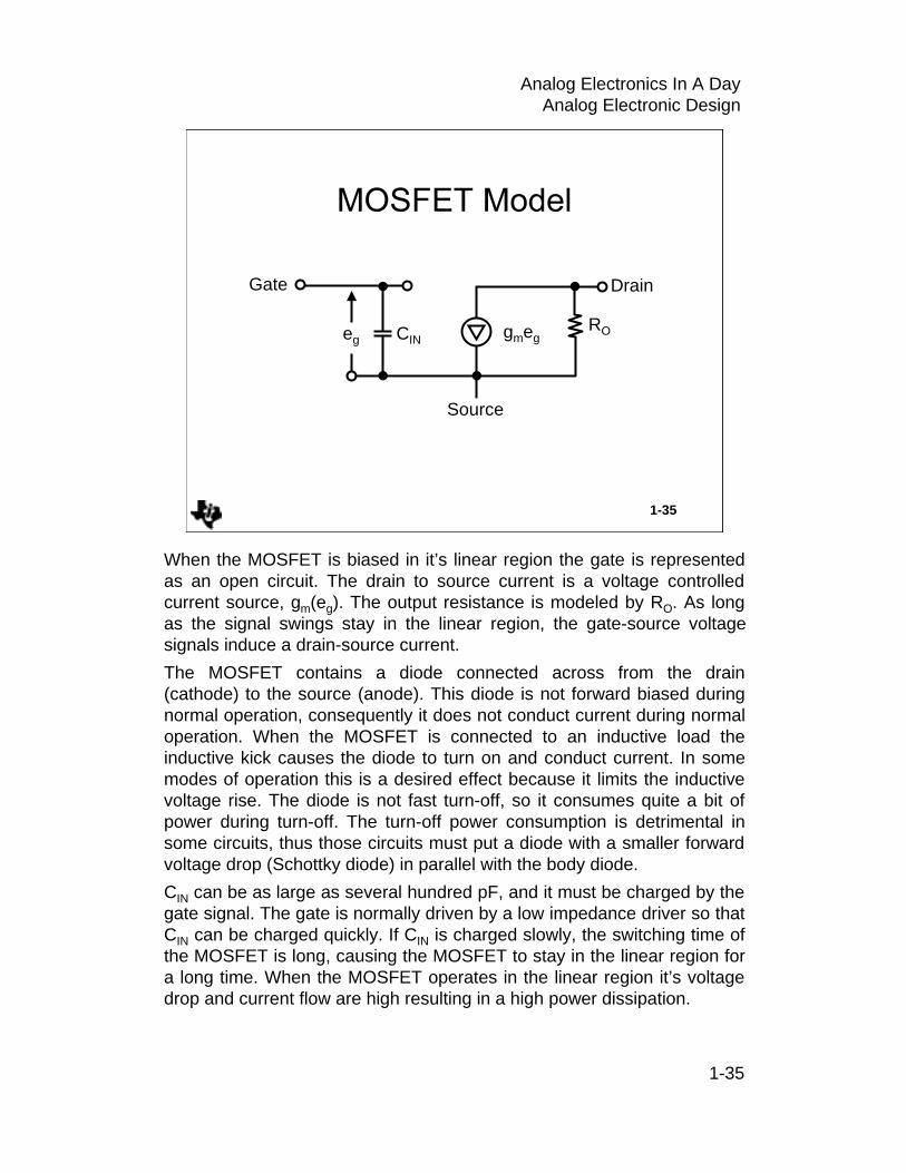
When the MOSFET is biased in it’s linear region the gate is represented as an open circuit. The drain to source current is a voltage controlled current source, gm(eg). The output resistance is modeled by RO. As long as the signal swings stay in the linear region, the gate-source voltage signals induce a drain-source current.
The MOSFET contains a diode connected across from the drain (cathode) to the source (anode). This diode is not forward biased during normal operation, consequently it does not conduct current during normal operation. When the MOSFET is connected to an inductive load theinductive kick causes the diode to turn on and conduct current. In some modes of operation this is a desired effect because it limits the inductive voltage rise. The diode is not fast turn-off, so it consumes quite a bit of power during turn-off. The turn-off power consumption is detrimental in some circuits, thus those circuits must put a diode with a smaller forward voltage drop (Schottky diode) in parallel with the body diode.
CIN can be as large as several hundred pF, and it must be charged by the gate signal. The gate is normally driven by a low impedance driver so that CIN can be charged quickly. If CIN is charged slowly, the switching time of the MOSFET is long, causing the MOSFET to stay in the linear region for a long time. When the MOSFET operates in the linear region it’s voltage drop and current flow are high resulting in a high power dissipation.

1-36
Analog Electronics In A DayAnalog Electronic Design
1-36
• Excellent precision• Made from BJT or FET• Good bandwidth• Very high initial gain• Gain roll-off starts quickly• High input impedance• Low output impedance
The voltage feedback operational amplifier (VF op amp), or op amp as it is affectionately known, is a versatile amplifier which requires feedback to function. The op amp gain is so high that the output saturates on any differential input signal, so feedback is employed to lower the closed loop gain. The feedback makes the op amp circuit a precision circuit because the gain becomes dependent on the passive components which can be very accurate. Some op amp parameters, such as input offset voltage can still degrade the precision, but there are specially designed precision op amps that have very low input offset voltages (micro volts), and selected salient parameters chosen to yield a precision circuit.
Op amp bandwidth depends on the process used to make the op amp,and BJT op amps are highest bandwidth and current drain, with JFET op amps being next, and MOSFET op amps have the lowest bandwidth and current drain. Voltage feedback op amps are discussed in this section, and their bandwidth starts rolling off at low frequencies (about five decades before the advertised gain-bandwidth point.
The input impedance of the VF op amps is very high, and their output impedance is relatively low, thus they ideal for configuring many different circuits. Some the possible circuits op amp can make are inverting amplifiers, non-inverting amplifiers, differential amplifiers, summing amplifiers, integrating amplifiers, and a host of others.

1-37
Analog Electronics In A DayAnalog Electronic Design
1-37
V+
PositiveInput
V-
NegativeInput
VOUT
A(V+-V-)
The input impedance of VF op amps is very high, and it is often modeled as an open circuit. The output circuit consists of a voltage controlled voltage source, and the control voltage is the differential voltage applied across the inputs.

1-38
Analog Electronics In A DayAnalog Electronic Design
1-38
• Medium precision• Made from BJT• Excellent bandwidth• Medium initial gain• Gain roll-off starts later• High or low input impedance• Very low output impedance
Current feedback op amps (CF op amp) are also called op amps, hence there can be confusion about which type of op amp (voltage or current feedback) is under discussion. It is assumed that voltage feedback op amps are being discussed unless a reference is made to the current feedback op amp. There are several reasons why CF op amps do notachieve the precision that VF op amps do: the applications for CF op amps generally do not require high precision, and the CF op amp configuration makes it hard to achieve precision. CF op amps are used for high frequency applications where the dc portion of the signal does not contain information, thus precision is not important in these applications. The input structure of a CF op amp is not matched, hence it is hard to obtain dc precision under these conditions.
CF op amps are usually made with BJTs because they yield very high bandwidths. The high bandwidth of a CF op amp does not start rolling off till much higher frequencies (several decades), and it rolls off at a much faster rate. CF op amps have bandwidths in the GHz range while VF op amp bandwidths are down in the several hundred MHz range.
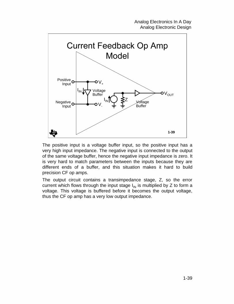
The input impedance of CF op amps is high for the positive input and low for the negative input because there is a voltage buffer between the inputs.
1-39
Analog Electronics In A DayAnalog Electronic Design
1-39
VOUT
IIN VoltageBuffer
Z
V+Positive
Input
V-Negative
Input
IIN VoltageBuffer
The positive input is a voltage buffer input, so the positive input has a very high input impedance. The negative input is connected to the output of the same voltage buffer, hence the negative input impedance is zero. It is very hard to match parameters between the inputs because they are different ends of a buffer, and this situation makes it hard to build precision CF op amps.
The output circuit contains a transimpedance stage, Z, so the error current which flows through the input stage IIN is multiplied by Z to form a voltage. This voltage is buffered before it becomes the output voltage, thus the CF op amp has a very low output impedance.

1-40
Analog Electronics In A DayAnalog Electronic Design
1-40
• Has an op amp front end bolted onto a digital backend
• Used to convert analog signals to digital signals
• Simplest form of the analog-to-digital converter
• Fast propagation speeds
The voltage comparator is used to convert an analog signal to a digital signal. This is usually accomplished by connecting a reference to one comparator input and a signal to the other input. When the signal exceeds the reference the output changes state. Inverted operation can be obtained with a comparator.
The input stage of a comparator is similar to an op amp input stage. The differential input voltage is multiplied by the gain to obtain an output signal. The comparator gain is very large, and it is not limited by feedback, so the output would saturate if it was an op amp. The difference is that the comparator has an output stage that reaches a limit but does not saturate. The comparator’s ability to run open loop without saturating separates it from the op amp which always saturates when it runs open loop. Never use op amps as comparators when the propagation delay is important, because when an op saturates the time it takes for the op amp to come out of saturation is unpredictable.

1-41
Analog Electronics In A DayAnalog Electronic Design
1-41
V+Positive
Input
V-Negative
Input
OutputVEEA(V+-V-)
VCC
The voltage comparator input stage is identical to a VF op amp input stage, consequently the comparator input impedance is very high. The inputs can be matched very well, thus comparators are capable of doing precision work. The voltage comparator output stage looks like a very high open loop gain stage that has it’s output clamped to the power supply rails. There are other forms of the output stage which have two leads, and they enable the circuit designer to connect the output to two different voltage levels. This type of comparator is useful when the input must sense signals over a wide voltage range including negative voltages, and the output voltage swing must be compatible with a specific logic family.

1-42
Analog Electronics In A DayAnalog Electronic Design
1-42
Although this seminar tries to minimize math and physics, some of each is required to understand analog electronics. Math and physics are presented in this seminar in the manner in which they are used later, so the shortest amount possible time is spent on these subjects.

1-43
Analog Electronics In A DayAnalog Electronic Design
1-43
• Ohm’s LawV = IR
• Kirchoff’s V LawΣ VSOURCE = Σ VDROP
• Kirchoff’s I LawΣ IJUNCTION = 0
VR1
R1
R2VR2V
R VI
I4I3
I1I2
Ohm’s law, V=IR, is fundamental to all electronics. It can be applied to a single component or to a complete circuit. When the current flowing through any portion of a circuit is known, the voltage dropped across that portion of the circuit is obtained by multiplying the current times the resistance.
Kirchoff’s voltage law states that the sum of the voltage drops in a series circuit equals the sum of the voltage sources. When taking sums keep in mind that the sum is an algebraic quantity.
Kirchoff’s current law states; the sum of the currents entering a junction equal the sum of the currents leaving a junction. It makes no difference if a current comes from a current source or through a resistor because all currents are treated equal.
1-44
Analog Electronics In A DayAnalog Electronic Design
1-44
• Assumes that R2is not loaded
21
2D( )
( )
( ) ( )21
22
212D
21
2121
RRR
VRRR
VIRV
RRV
I
RRIIRIRV
+=
+==
+=
=+= +
V
R1
II R2 VD
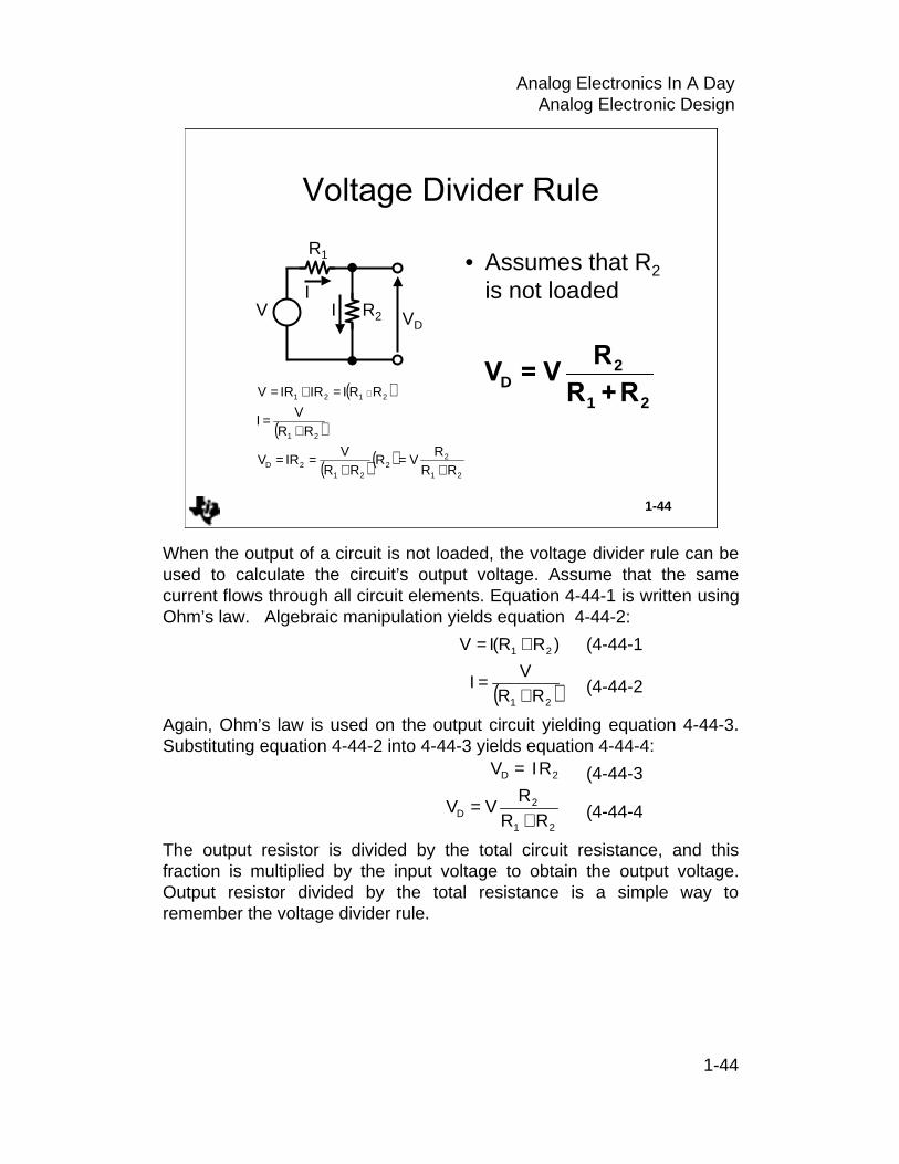
When the output of a circuit is not loaded, the voltage divider rule can be used to calculate the circuit’s output voltage. Assume that the same current flows through all circuit elements. Equation 4-44-1 is written using Ohm’s law. Algebraic manipulation yields equation 4-44-2:
(4-44-1
(4-44-2
Again, Ohm’s law is used on the output circuit yielding equation 4-44-3. Substituting equation 4-44-2 into 4-44-3 yields equation 4-44-4:
(4-44-3
(4-44-4
The output resistor is divided by the total circuit resistance, and this fraction is multiplied by the input voltage to obtain the output voltage. Output resistor divided by the total resistance is a simple way to remember the voltage divider rule.
( )21
21
RRV
I
)RR(IV
+=
+=
21
2D
2D
RRR
VV
R I V
+=
=

1-45
Analog Electronics In A DayAnalog Electronic Design
1-45
• Assumes no load besides R1 and R2I I1 R1 VR2
I2
21
12 +
=
21
12
1
212
1
222
1
2221
1
221
2211
21
RRR
II:Then
RRR
IRR
IIIRR
IIII
RR
II
RIRIV
III
+=
+=
+=+=+=
=
=== +
When the output of a circuit is not loaded, the current divider rule can be used to calculate the current flow in the output component. The currents I1 and I2 are assumed to be flowing in the branch circuit. Equation 4-45-1 is written with the aid of Kirchoff’s current law. The circuit voltage is written in equation 4-45-2 with the aid of Ohm’s law. Combining equations 4-45-1 and 4-45-2 yields equation 4-45-3:
(4-45-1
(4-45-2
(4-45-3
Rearranging the terms in equation 4-45-3 yields equation 4-45-4:
(4-45-4
The total circuit current divides into two parts, and the resistance, R1, divided by the total resistance determines how much current flows through R2. A way to remember the current divider rule is that the opposite resistor is divided by the total resistance.
+=
+=+
=+=
==+=
1
212
1
222
1
2221
22 11
21
RRR
IRR
1IIRR
IIII
R IR IV
I II
21
12 RR
RII
+=

1-46
Analog Electronics In A DayAnalog Electronic Design
1-46
• Employed to isolate some part of the circuit
• Results in a simplified equivalent circuit
• Much quicker analysis
• If input is a voltage source use Thevenin’s theorem
• If input is a current source use Norton’s theorem
There are times when it is advantageous to isolate a part of the circuit. Rather than write loop or node equations and solving them simultaneously, Thevenin’s theorem enables us to isolate part of the circuit we are interested in. We then replace the remaining circuit with a simple series equivalent circuit, thus Thevenin’s theorem simplifies the analysis.
There are two theorems that do the similar functions, and the second theorem is called Norton’s theorem. Thevenin’s theorem is used when the input is a voltage source, and Norton’s theorem is used when the input is a current source. Norton’s theorem is rarely used, so its explanation is left to outside sources.

1-47
Analog Electronics In A DayAnalog Electronic Design
1-47
• Look into the terminals of the components being replaced
• Calculate the no load open circuit voltage
• Short independent voltage, open independent current sources
• Calculate the impedance
• Replace original circuit with Thevenin
The rules for Thevenin’s theorem start with the component or part of the circuit being replaced. Look into the terminals of the circuit being replaced, and calculate the no load voltage as seen from these terminals (much like calculating a voltage divider). Again, looking into the terminals of the circuit being replaced, short independent voltage sources, and calculate the impedance between these terminals. Now, the next step is to substitute the Thevenin equivalent circuit for the circuit part you wanted to replace.
The Thevenin equivalent circuit is a simple series circuit; thus further calculations are simplified. The simplification of circuit calculations is often sufficient reason to use Thevenin’s theorem because it eliminates the need for solving several simultaneous equations. The detailed information about what happens in the circuit that was replaced is not available when using Thevenin’s theorem, but that is of no consequence because you had no interest in it.

1-48
Analog Electronics In A DayAnalog Electronic Design
1-48
THE ORIGINAL CIRCUIT
THE THEVENIN EQUIVALENT CIRCUIT
VR1
R2 VO
R3
R4
Vth
Zth
VO
R3
R4
21
2th RR
RVV
+=
2121
21yxth RR
RRRR
ZZ ≡+
== −
4321
21
4
21
2
43th
4th0
RRRR
RRR
RRR
V
RRZR
VV
+++
+=
++=
XY
XY
In this example we want to calculate the output voltage, VO. The first step is to stand on the terminals X-Y with your back to the output circuit, and calculate the open circuit voltage seen. This is a perfect opportunity to use the voltage divider rule to obtain equation 4-7-1.
(4-48-1
Still standing on the terminals X-Y, step two is to calculate the impedance seen looking into these terminals. The Thevenin impedance is the parallel impedance of R1 and R2 as calculated in equation 4-48-2.
(4-48-2
Now get off the terminals X-Y before you damage them with your big feet. Step three replaces the circuit to the left of X-Y with the Thevenin equivalent circuit Vth and Rth.
The final step is to calculate the output voltage. Notice the voltage divider rule is used again. Equation 4-48-3 describes the output voltage, and it comes out naturally in the form of a series of voltage dividers, which makes sense. That’s another advantage of the voltage divider rule; that the answers normally come of in a recognizable form rather than a jumble of coefficients and parameters.
(4-48-3
21
2th RR
RVV
+=
2121
21yxth RR
RRRR
ZZ ≡+
== −
4321
21
4
21
2
43th
4th0
RRRR
RRR
RRR
V RRZ
RVV
+++
+=
++=
1-49
Analog Electronics In A DayAnalog Electronic Design
1-49
( )( )
( ) ( )
( )
( )( )2
2
21432
40
420
2212
4322
22212
4322
22
4321
214322
22211
RR
RRRRRR
VV
RIV
RRRR
RRRV
I
RIRRR
RRRIV
IR
RRRI
RIRRRI
RIRRIV
−+++=
=
−+++=
−+++=
++=
=++−+=
V
R1
R2
V0
R3
R4I1 I2
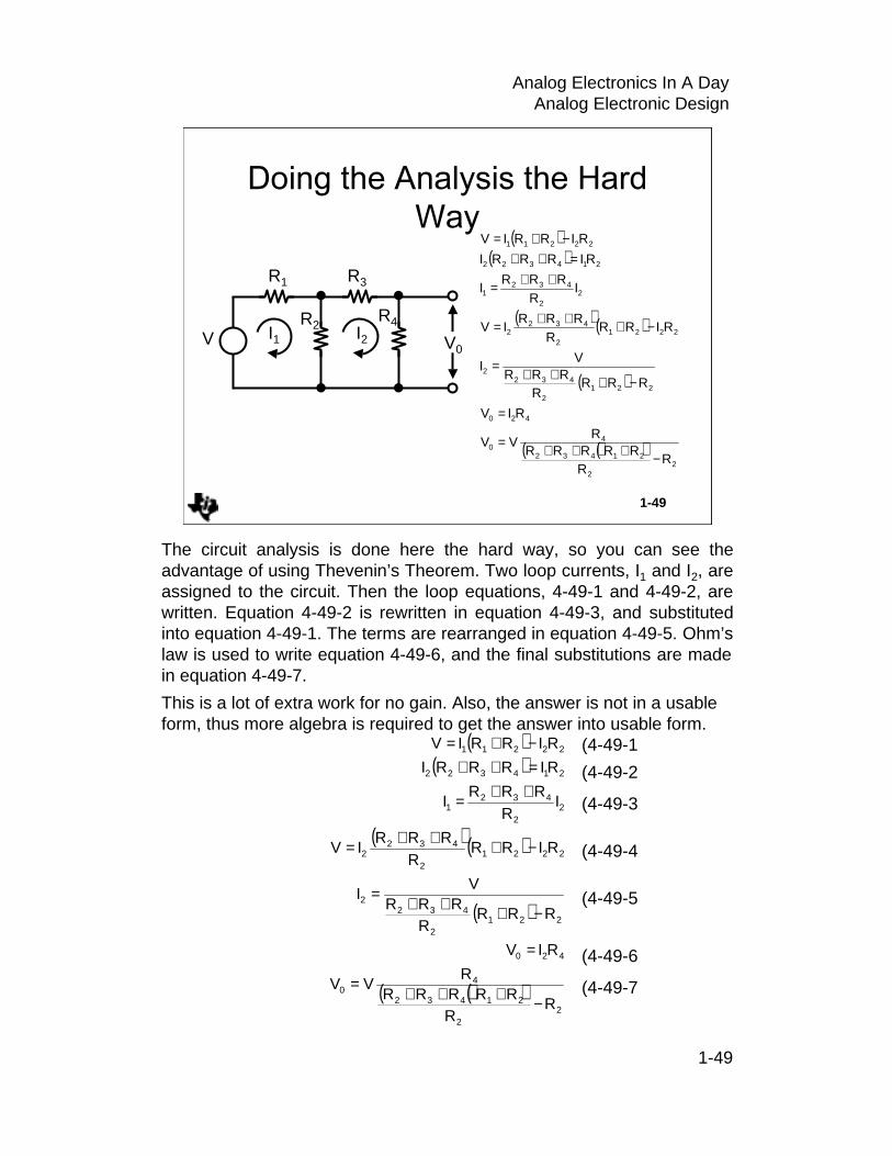
The circuit analysis is done here the hard way, so you can see the advantage of using Thevenin’s Theorem. Two loop currents, I1 and I2, are assigned to the circuit. Then the loop equations, 4-49-1 and 4-49-2, are written. Equation 4-49-2 is rewritten in equation 4-49-3, and substituted into equation 4-49-1. The terms are rearranged in equation 4-49-5. Ohm’s law is used to write equation 4-49-6, and the final substitutions are made in equation 4-49-7.
This is a lot of extra work for no gain. Also, the answer is not in a usable form, thus more algebra is required to get the answer into usable form.
(4-49-1
(4-49-2
(4-49-3
(4-49-4
(4-49-5
(4-49-6
(4-49-7
( )( )
( ) ( )
( )
( )( )2
2
21432
40
420
2212
4322
22212
4322
22
4321
214322
22211
RR
RRRRRR
VV
RIV
RRRR
RRRV
I
RIRRR
RRRIV
IR
RRRI
RIRRRI
RIRRIV
−+++=
=
−+++=
−+++=
++=
=++−+=

1-50
Analog Electronics In A DayAnalog Electronic Design
1-50
V1
R3VO
R2
V2
R1
2213
21O
1
VRRR
RRV
0V When
+=
=
213
212
321
32102010 RRR
RRV
RRR
RRVVVV
++
+=+=
1321
32O
2
VRRR
RRV
0V When
+=
=
Superposition is a theorem that can be applied to any linear circuit. Essentially, when there are independent sources, the voltages and currents resulting from each source can be calculated separately, and the results are added algebraically. This simplifies the calculations because it keeps from having to write a series of loop or node equations.
When V2 = 0 or is grounded, V1 forms a voltage divider with R1 and the parallel combination of R2 and R3. The voltage divider theorem yields the answer quickly. Likewise, when V1 = 0, V2 forms a voltage divider with R3and the parallel combination of R1 and R2, and the voltage divider theorem is applied again. After the calculations for each source are made the components are added to obtain the final solution.
The reader should analyze this circuit with loop or node equations, and then they are sure to become a fan of superposition. Again, the superposition results come out is a simple arrangement that is easy to understand. One looks at the final equation and it is obvious that if the sources are equal and opposite polarity, and R1 =R3, then the output voltage is zero. Conclusions such as this are hard to make after the results of a loop or node analysis unless considerable effort is made to manipulate the final equation into symmetrical form.

1-51
Analog Electronics In A DayAnalog Electronic Design
1-51
VIN
IB
RB
+12V
RC
VOUT
IC
The high level collector equation is calculated in equation 4-51-1. Also, the minimum current gain is 30.
(4-51-1
The required base current is calculated in equation 4-51-2.
(4-51-2
Resistor conditions: VIN = 12V, VOUT <0.2V
VIN < 0.05V, VOUT > 10V at IC = 10mA
( ) ( )K2.34
10306.012
IVV
RC
BE12B =−=β−≤ +
Ω=−=−= + 200K10
1012I
VVR
C
OUT12C

1-52
Analog Electronics In A DayAnalog Electronic Design
1-52
+12V +12V
21
21B RR
RRR
+=
CIN
VIN
R2
R1
RE1
RE2 CE
VOUT
RC
The specifications are for a stable amplifier which has a gain of four and output voltage swing of four volts peak-to-peak. The bias point is chosen as Vc=6V because this enables the transistor to swing positive 4 volts without cutting the transistor off. Let IC = 10mA, the output signal is shown symmetrical, and the transistor has a minimum βac = 50 and βdc 100.
(3-52-1
Let VCE = 6V so the transistor can swing negative four volts without saturating the transistor; then (RE1 + RE2) = VE/IC = 600Ω. The base voltage must be VB = VE + VBE + IB(RB), so R1 and R2 are calculated to yield VB and RB. The ac gain equation is G = RC/RE1. Now RE1 and RE2can be calculated.
This design makes numerous assumptions, but when β is high the assumptions are valid. Different types of transistors could be used for the amplifier, but similar assumptions can be made to speed their design. This amplifier has easy specifications, but it is hard to meet stringent specifications with a single transistor, thus integrated circuit amplifiers are used to do the hard jobs.
Ω=−=−= + 60010
612I
VVR
C
C12c

1-53
Analog Electronics In A DayAnalog Electronic Design
1-54
Analog Electronics In A DayAnalog Electronic Design
1-54
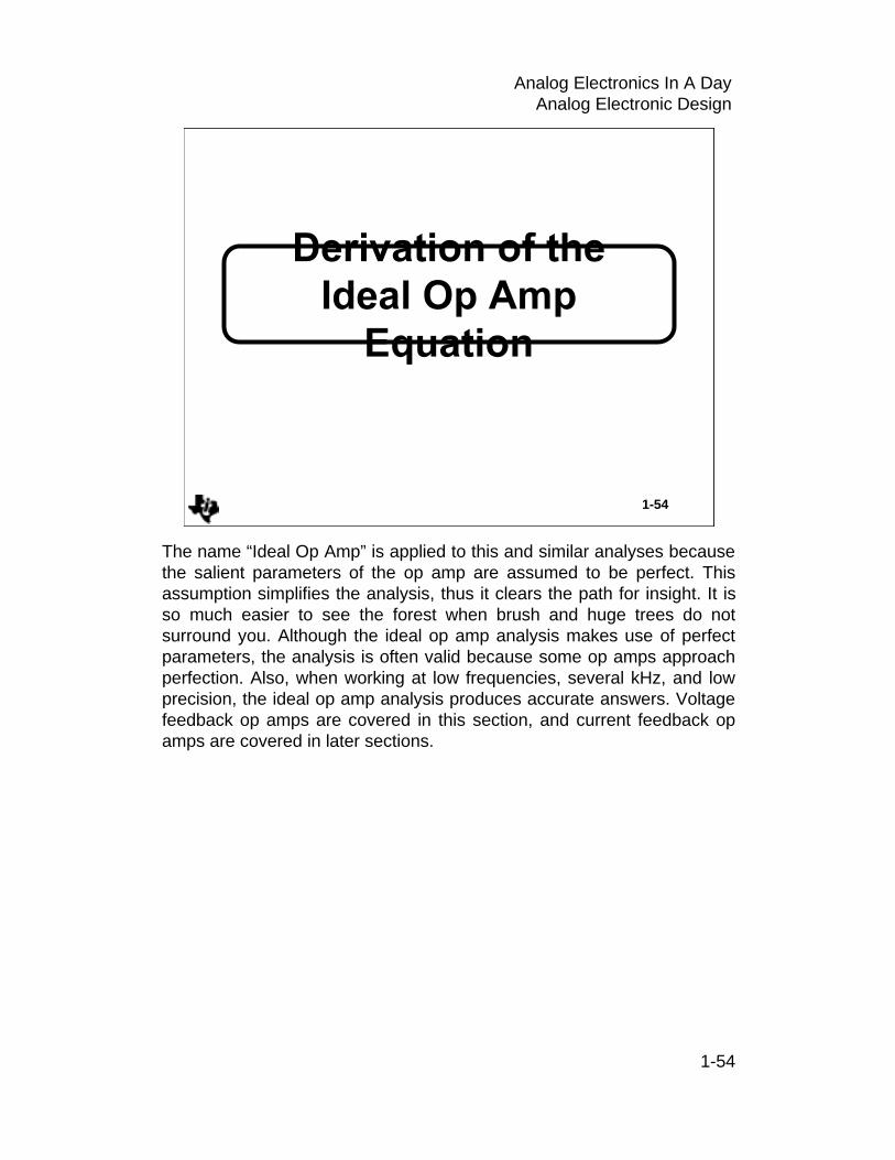
The name “Ideal Op Amp” is applied to this and similar analyses because the salient parameters of the op amp are assumed to be perfect. This assumption simplifies the analysis, thus it clears the path for insight. It is so much easier to see the forest when brush and huge trees do not surround you. Although the ideal op amp analysis makes use of perfect parameters, the analysis is often valid because some op amps approach perfection. Also, when working at low frequencies, several kHz, and low precision, the ideal op amp analysis produces accurate answers. Voltage feedback op amps are covered in this section, and current feedback op amps are covered in later sections.

1-55
Analog Electronics In A DayAnalog Electronic Design
1-55
• The current flow in the input leads is zero.
• The gain is infinite.
• The gain drives the output voltage until the voltage across the input leads equals zero.
• The output impedance is zero.
• The frequency response is flat.
Several assumptions have to be made before the ideal op amp analysis can proceed. First assume that the current flow into the input leads is zero. This assumption is almost true in FET op amps where input currents can be less than a pA, but this is not always true in in bipolar high speed op amps where input currents in the tens of µA are found. The gain is assumed to be infinite, hence it drives the output voltage to any value required to satisfy the input conditions. This assumes that the op amp output voltage can achieve any value, but saturation occurs when the output voltage comes close to a power supply rail. Reality doesn’t negate the assumption; it only bounds it. Also, implicit in the infinite gain assumption is the need for a minuscule input signal.
The gain drives the output voltage until the voltage between the input leads (the error voltage) is extremely small. This leads to a further assumption that the voltage between the input leads is zero. Theimplication of zero voltage between the input leads means that if one input is tied to a hard voltage source such as ground the other input is at the same potential. There may be an offset voltage between the input leads, but it is ignored in this analysis. The current flow into the input leads is zero, so the input impedance of the op amp in infinite.
Two final assumptions are that the output impedance is zero, and that the frequency response is flat (does not vary as frequency changes). The output impedance of most op amps is a fraction of an ohm for low current flows, so this assumption is valid. By constraining the use of the op amp to the low frequencies, we make the frequency response assumption true.

1-56
Analog Electronics In A DayAnalog Electronic Design
1-56
VIN
I1
RG
IB
IB
VE
I2
RF
-+
a VOUT
G
F
IN
OUT
GOUTFIN
F
OUT2
G
IN1
RR
VV
RVRV
RV
IRV
I
−=
−=
−=−==Assume IB = 0,
VE = 0,
a = ∞
Then:
The non-inverting input of the inverting op amp is grounded, hence because of the assumption that the input error voltage is zero, the inverting input of the op amp is at ground (actually it is held at a virtual ground by the feedback). Also, the current flow in the input leads is assumed to be zero, so the current flowing through RG equals the current flowing through RF, and we can use Kirchoff’s law to write equation 5-56-1.
Algebraic manipulation gives us equation 5-56-3. Notice that the output signal is only a function of the feedback and gain resistors, so the feedback has accomplished it’s function of making the gain independent of the op amp parameters. The gain can be adjusted by varying the value of either resistor. One final note; the output signal is the input signal amplified and inverted. The input impedance is set by RG because the inverting input lead is held at a virtual ground.
(5-56-1
(5-56-2
(5-56-3G
F
IN
OUT
GOUTFIN
F
OUT2
G
IN1
RR
VV
RVRV
RV
IRV
I
−=
−=
−=−==
1-57
Analog Electronics In A DayAnalog Electronic Design
1-57
VIN
RG
VE
RF
VOUT
VINX
G
GF
IN
OUT
GF
GOUTIN
RRR
VV
RRRV
V
+=
+=
+a
-
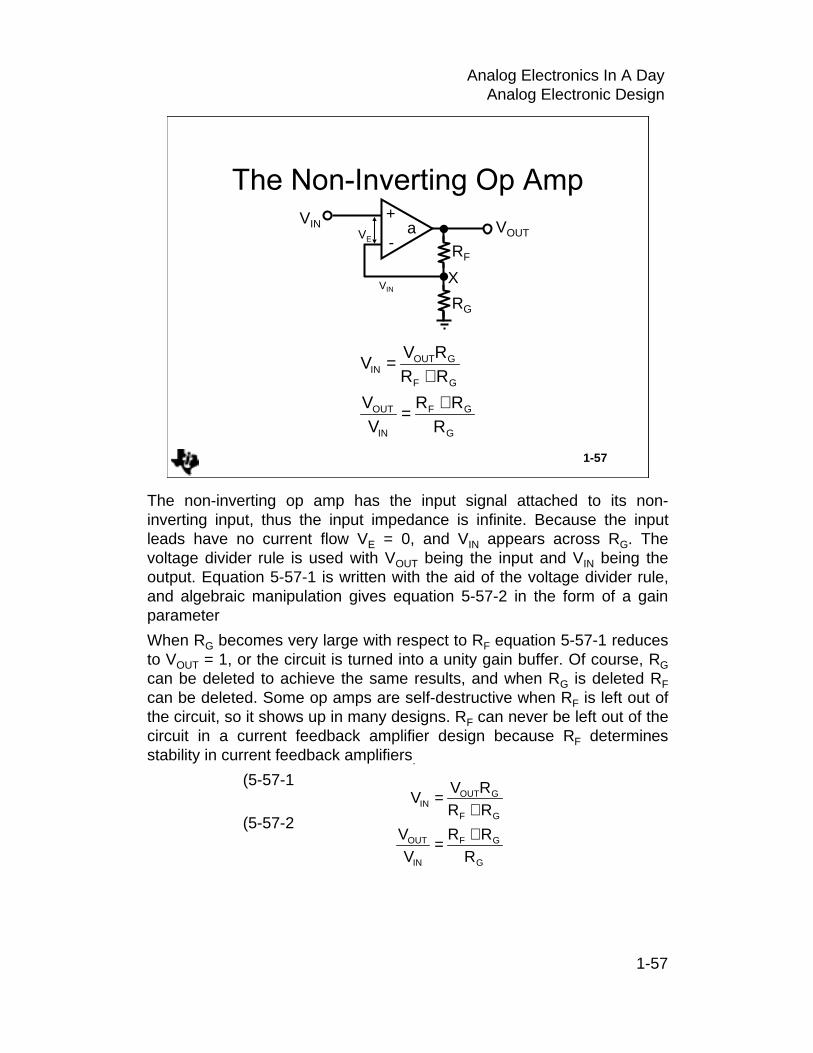
The non-inverting op amp has the input signal attached to its non-inverting input, thus the input impedance is infinite. Because the input leads have no current flow VE = 0, and VIN appears across RG. The voltage divider rule is used with VOUT being the input and VIN being the output. Equation 5-57-1 is written with the aid of the voltage divider rule, and algebraic manipulation gives equation 5-57-2 in the form of a gain parameter
When RG becomes very large with respect to RF equation 5-57-1 reduces to VOUT = 1, or the circuit is turned into a unity gain buffer. Of course, RGcan be deleted to achieve the same results, and when RG is deleted RFcan be deleted. Some op amps are self-destructive when RF is left out of the circuit, so it shows up in many designs. RF can never be left out of the circuit in a current feedback amplifier design because RF determines stability in current feedback amplifiers.
(5-57-1
(5-57-2
G
GF
IN
OUT
GF
GOUTIN
RRR
VV
RRRV
V
+=
+=

1-58
Analog Electronics In A DayAnalog Electronic Design
1-58
V1
R1
V2
R3
R2
V+
V-
-+
a
R4
VOUT
3
42
3
43
12
21OUT
3
422OUT
3
43
21
21OUT
21
21
3
4
1OUT
RR
VR
RRRR
RVV
RR
VV
RRR
RRR
VV
RRR
VVRR
1VV
1
−
++
=
−=
++
=
+=
+= ++
The differential amplifier amplifies the difference signal applied to the input circuit, and it rejects the common mode portion of the input. This circuit configuration is often employed to strip dc or injected common mode noise off a signal. Superposition is used to calculate the output voltage resulting from each input voltage, and then the two output voltages are added to arrive at the final output voltage.
The output voltage resulting from V1 is calculated in equation 5-58-1. The voltage divider rule is used to calculate V+, and the non-inverting gain equation is used to calculate the stage gain. The inverting gain equation is used to calculate the stage gain for V2 in equation 5-58-3. These gains are added in equation 5-58-4.
(5-58-1
(5-58-2
(5-58-3
−=
++
=
+=
+= ++
3
422OUT
3
43
21
21OUT
21
21
3
4
1OUT
RR
VV
RRR
RRR
VV
RRR
V VRR
1VV
1

1-59
Analog Electronics In A DayAnalog Electronic Design
If we let R2 = R4 and R1 = R3, equation 5-5-4 reduces to VOUT = (V1-V2)(R4/R3). It is now obvious that the differential signal, (V1-V2), is multiplied by the stage gain. The disadvantage of this circuit is that the two input impedances can’t be matched and have it act as a differential amplifier, thus there is a two op amp version of this circuit specially designed for high performance differential applications.
(5-5-43
42
3
43
12
21OUT R
RV
RRR
RRR
VV −
++
=

1-60
Analog Electronics In A DayAnalog Electronic Design
1-60
VINR1 R2
+a
-
XYR4
R3
VOUT
VINR1 R2
+a
-
Rth
Vth
1
th2
IN
th
43th
43
4Oth
RRR
VV
RRR
RRRV
V
+=−
=+
=
1
4
3232
4
43
1
43
432
4
43
1
th2
IN
OUT
RRRR
RR
RRR
RRR
RRR
RRR
RRR
V
V
+=
+++
=
++=−
Sometimes it is desirable to have a low resistance path to ground in the feedback loop. Standard inverting op amps can’t do this when the driving circuit sets the input resistor value, and the gain specification sets the feedback resistor value. Inserting a “T” network in the feedback loop yields a degree of freedom that enables both specifications to be met with a low dc resistance path in the feedback loop.
Break the circuit at point X-Y, and calculate the Thevenin equivalent voltage as shown in equation 5-60-1. The Thevenin equivalent is impedance calculated in equation 5-60-2. Replace the output circuit with the Thevenin equivalent circuit, and calculate the gain with the aid of the inverting gain equation as shown in equation 5-60-3.
(5-60-1
(5-60-2
(5-60-3
Substituting the Thevenin equivalents into equation 5-60-3 yields equation 5-60-4 (see page 5-8).
1
th2
IN
th
43th
43
4Oth
RRR
VV
RRR
RRRV
V
+=−
=+
=

1-61
Analog Electronics In A DayAnalog Electronic Design
(5-7-4
Specifications for the circuit you are required to build are an inverting amplifier with an input resistance of 10K (RG = 10K), a gain of 100, and a feedback resistance path to ground of 20K or less. The inverting op amp circuit can’t meet these specifications because RF must equal 1000K. Inserting a “T” network with R2 =R4= 10K and R3 = 445K does meet the specifications.
1
4
3232
4
43
1
43
432
4
43
1
th2
IN
OUT
RRRR
RR
RRR
RRR
RRR
RRR
RRR
V
V
+=
+++
=
++=−

1-62
Analog Electronics In A DayAnalog Electronic Design
1-62
TM
T
G
GF
IN
OUT
RRR
RRR
VV
++=
RG
RIN
RF
VOUTRM
RT
VIN+
a-
Video signals contain high frequencies, and the cable connecting the circuits has a characteristic impedance of 75Ω, so the input and output circuit impedances should be 75Ω to match the cable. Matching the cable impedance is required to prevent reflections because reflections cause severe disturbances in video signals.
Matching the input impedance is simple for a non-inverting amplifier because its input impedance is very high; just make RIN = 75Ω. RF and RGcan be selected as very high values, in the KΩ range, so that they won’t affect the output circuit. A resistor, RM, is placed in series with the op amp output to raise its output impedance to 75Ω, a terminating resistor, RT, is placed at the input of the next stage to match the cable. The matching and terminating resistors are equal in value, and they form a voltage divider of ½. Very often RF is selected equal to RG so that the system gain is equal to one (2 x ½ = 1).
TM
T
G
GF
IN
OUT
RRR
RRR
VV
++=

1-63
Analog Electronics In A DayAnalog Electronic Design
1-63
• Inductors are not considered.
• Capacitors have an impedance equal to:
• If f goes to zero XC becomes infinite.
• If f goes to infinity XC becomes zero.
fC21
XC π=
Capacitors are a key component in a circuit designer’s toolkit, thus a short discussion on evaluating their effect on circuit performance is in order. Capacitors have an impedance of XC = 1/(2πfC). Note that when the frequency is zero the capacitive impedance (also known as reactance) is zero, and that when the frequency is infinite the capacitive impedance is zero.

1-64
Analog Electronics In A DayAnalog Electronic Design
1-64
VIN
RGRF-
+a VOUT
CF
-+
a VOUT
VIN
RF
RG CG
LOW PASS FILTER
HIGH PASS FILTER
CAPACITOR IMPEDANCE
CXC
The low pass filter circuit has a capacitor in parallel with the feedback resistor. At very low frequencies XC ⇒ α, so the capacitor has no effect. At very high frequencies XC ⇒ 0, so the feedback resistor is shorted out thus reducing the circuit gain to one. At the frequency where XC = RF the gain is reduced to half.
Connecting the capacitor in parallel with RG where it has the opposite effect can make a high pass filter. This simple technique is used to predict the form of a circuit transfer function rapidly. Better analysis techniques are presented later for those applications requiring more precision.

1-65
Analog Electronics In A DayAnalog Electronic Design

1-66
Analog Electronics In A DayAnalog Electronic Design
1-66
Block DiagramsBode Plots
Second Order Equation
Analysis tools have something in common with medicine because they both can be distasteful but necessary. Medicine often tastes bad or has undesirable side effects, and analysis tools involve lots of hard learning work before they can be applied to yield results. Medicine gives your body assistance in fighting an illness; analysis tools give your brain assistance in learning/designing feedback circuits.
The analysis tools given here are a synopsis of the salient points, thus they are detailed enough to get you where you are going without any extras. The references along with thousands of their counterparts must be consulted when making an in depth study of the field. Aspirin, home remedies, and good health practice handle the majority of healthproblems, and these analysis tools solve the majority of circuit problems.

1-67
Analog Electronics In A DayAnalog Electronic Design
1-67
• Shorthand pictorial representation of the
cause and effect relationship between input
and output in a real system.
• Convenient method for characterizing the
functional relationships between components.
• No understanding of details within the block.
Block diagrams have a unique algebra and set of transformations, and they are used to represent electronic systems and circuits. The block diagrams are used because they are a shorthand pictorial representation of the cause and effect relationship between the input and output in a real system. They are a convenient method for characterizing the functional relationships between components. You do not need to understand the functional details of a block to manipulate a block diagram.

1-68
Analog Electronics In A DayAnalog Electronic Design
1-68
• Input impedance is high — no loading• Output impedance is zero — high fan-out• Arrows show signal flow• Blocks do all math except add and subtract
CONTROLELEMENTCONTROLELEMENT
INPUT OUTPUT
XDTD DT
DXY =
The input impedance of each block is assumed to be infinite to preclude loading. Also, the output impedance of each block is assumed to be zero to enable high fan-out. The systems designer sets the actual impedance levels, but the fan-out assumption is valid because the block designers adhere to the system designer’s specifications. All blocks multiply the input times the block quantity unless otherwise specified within the block. The quantity within the block can be a constant, or it can be a complex math function involving LaPlace transforms. The blocks can perform time-based operations such as differentiation and integration.

1-69
Analog Electronics In A DayAnalog Electronic Design
1-69
X X - Y+
-
Y
(b) X X+Y+Z+
+
Y
+
Z
(c)
• Summing points add and subtract• Unlimited inputs• Mixed signs OK
X X + Y+
+
Y
(a)
Adding and subtracting are performed in special blocks called summing points. Several examples of summing points are given in the figure. Please note that summing points have unlimited inputs, they can add or subtract, and they can have mixed signs yielding addition and subtraction within a single summing point.

1-70
Analog Electronics In A DayAnalog Electronic Design
1-70
+R + G1 G4 G2
G3
+
+
C
H1
+
H2
-
H2
-
+R
1H4G1G13G2G4G1G
−+
C
Multiple loop feedback systems are intimidating, but they can be reduced to a single loop feedback system by writing equations and solving for VOUT/VIN. The equation for each point in the loop is written, and the equations are solved to obtain the simplified result. Reducing multiple loops to a single loop loses some information, but when you are interested in a single parameter such as stability the lost information has no value.

1-71
Analog Electronics In A DayAnalog Electronic Design
1-71
• Combine cascade blocks
• Combine parallel blocks
• Eliminate inside feedback loops
• Shift summing points to the left
• Shift takeoff points to the right
• Repeat until simple form is obtained
Follow the rules given below to reduce multiple loop feedback systems to single loop feedback systems.
The block diagram reduction rules are:
• Combine cascade blocks.
• Combine parallel blocks.
• Eliminate interior feedback loops.
• Shift summing points to the left.
• Shift takeoff points to the right.
Repeat until canonical form is obtained.

1-72
Analog Electronics In A DayAnalog Electronic Design
1-72
• The simplest form of the feedback loop
• Easy to analyze
• All feedback loops can be reduced to this form
• The canonical feedback loop exists for each input
• The response of each input can be analyzed separately
The idea behind the block diagram effort is to reduce the diagram to its canonical form because we know a lot about that form. The canonical feedback loop is the simplest form of a feedback loop, and its analysis is well documented. All feedback systems can be reduced to the canonical form, so all feedback systems can be analyzed with the same math. Be aware that a canonical loop exists for every input to a feedback system. Although the stability dynamics are independent of the input, the output performance is input dependent. Each input response in a multiple input feedback system can be analyzed separately, and then they are added through superposition to obtain the final response.

1-73
Analog Electronics In A DayAnalog Electronic Design
1-73
Σ
H
±
+R C
B
E G
GH1GH
RB
GH11
RE
GH1G
RC
±=
±=
±=
The canonical form of a feedback loop is shown with control system and electronic system terms. The nomenclature of the variables, G or A, make no difference except to the system engineers, but the math does have meaning, and it is identical for both types of terms. The electronic terms and negative feedback sign are used in this analysis because subsequent application notes deal with electronic applications.

1-74
Analog Electronics In A DayAnalog Electronic Design
1-74
AAΣ
-
ββ
VINE
VOUT
( )
( )β+=
β+=
=
−=
=
A1
A1
A
1VE
AV
V
VE
VVE
EAV
IN
IN
OUT
OUT
OUTIN
OUT
β
The output equation and error equation are written below.
Combining these equations yields;
Rearranging terms puts the equation in recognizable form.
This is the classic form of the feedback equation.
Please notice that when the term, Aβ, in equation becomes large with respect to one the equation reduces to the ideal feedback equation, and it finds extensive use when amplifiers are assumed to have ideal qualities. Under the conditions that Aβ>>1, the system gain is determined by the feedback factor β. Stable passive circuit components are used to implement the feedback factor, thus in the ideal situation, the closed loop gain is predictable and stable because β is stable and predictable.
OUTINOUT VVA
V β−=
INOUTV
A1
V =
β+
1AIN
OUT
IN
OUT
1V
V
A1A
VV
>>ββ
=
β+=
EA V, V-VE OUTOI =β=

1-75
Analog Electronics In A DayAnalog Electronic Design
1-75
Block Diagram For Computing The Loop Gain
A
β
VTOΣ VTI
-
180
11A
0A1
−=−=β
=β+
βAVV
TI
TO =
The quantity Aβ is so important that it has been given a special name, loop gain. Consider the figure; when the voltage inputs are grounded (current inputs are opened) and the loop is broken the calculated gain is the loop gain, Aβ. Now, keep in mind that this is a mathematics of complex numbers which have magnitude and direction. When the loop gain approaches minus one, or to express it mathematically 1∠180o, equation 7-1-5 approaches infinity because 1/0⇒∝. The circuit output heads for infinity as fast as it can using the equation of a straight line. If the output were not energy limited the circuit would explode the world, but it is energy limited by the power supplies so the world stays intact.
Active devices in electronic circuits exhibit non-linear behavior when their output approaches a power supply rail, and the non-linearity reduces the amplifier gain until the loop gain no longer equals 1∠180o. Now the circuit can do two things: first it could become stable at the power supply limit, or second, it can reverse direction (because stored charge keeps the output voltage changing) and head for the negative power supply rail.
The first state where the circuit becomes stable at a power supply limit is named lockup; the circuit will remain in the locked up state until power is removed. The second state where the circuit bounces between power supply limits is named oscillatory. Remember, the loop gain, Aβ, is the sole factor that determines stability for a circuit or system. Inputs are grounded or disconnected when the loop gain is calculated, so they have no affect on stability.

1-76
Analog Electronics In A DayAnalog Electronic Design
1-76
• Developed by H.W. Bode in 1945.
• Bode plots are log plots.
• Uses logs so equations can be added and subtracted graphically.
• 20Log(F(t)) = 20Log|F(t)| + Phase Angle
H. W. Bode developed a quick, accurate, and easy method of analyzing feedback amplifiers, and he published a book about his techniques in 1945. Op amps had not been developed when Bode published his book, but they fall under the general classification of feedback amplifiers, so they are easily analyzed with Bode techniques. The mathematical manipulations required to analyze a feedback circuit are complicated because they involve multiplication and division. The Bode plot simplifies the analysis through the use of graphical techniques.
The Bode equations are log equations which take the form 20LOG(F(t)) = 20LOG(F(t)) + phase angle. Taking the log of a function breaks the function into its component parts; the magnitude and the phase. Terms that are normally multiplied and divided can now be added and subtracted because they are log equations. The addition and subtraction is done graphically, thus easing the calculations and giving the designer a pictorial representation of circuit performance.
1-77
Analog Electronics In A DayAnalog Electronic Design
1-77
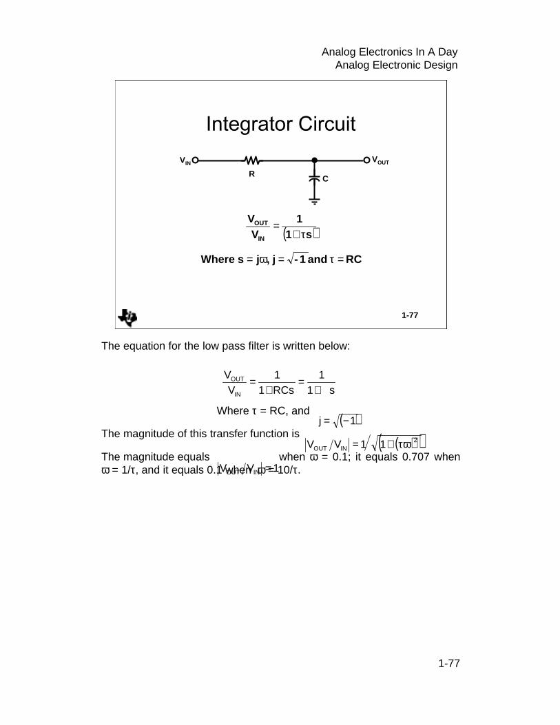
( )
RC and 1-j ,js Where
s11
VV
IN
OUT
===
+=
τω
τ
VIN VOUT
CR
The equation for the low pass filter is written below:
Where τ = RC, and
The magnitude of this transfer function is
The magnitude equals when ω = 0.1; it equals 0.707 when ω = 1/τ, and it equals 0.1 when ω = 10/τ.
s11
RCs11
VV
IN
OUT
+=
+=
( )1j −=
( )( )2INOUT 11VV τω+=
1VV INOUT =

1-78
Analog Electronics In A DayAnalog Electronic Design
1-78
0dB
-3dB
-20dB0°
-45°
-90°Ph
ase
Sh
ift
20L
og
(IV
O/V
II)
ω = 0.1/τ ω = 1/τ ω = 10/τ
-20dB/Decade
These points are plotted in figure 4-2 using straight-line approximations. The negative slope is -20dB/decade or -6dB/octave. The magnitude curve is plotted as a horizontal line until it intersects the breakpoint where ω = 1/τ. The negative slope begins at the breakpoint because the magnitude decreases rapidly at that point. The gain is equal to 1 or 0dB at very low frequencies, equal to 0.707 or -3db at the break frequency, and it keeps falling with a -20db/decade slope for higher frequencies.
The phase shift for the low pass filter or any other transfer function is calculated as shown below:
The phase shift is much harder to draw on a Bode plot because the tangent function is non-linear. The phase information around the 0dB intercept point yields the stability information for an active circuit, so the phase calculations are only done at the point near the 0dB crossover. The phase is approximated by remembering that the tangent of 90o is 1, the tangent of 60o is , and the tangent of 30o is .
A breakpoint occurring in the denominator is called a pole, and it slopes down. Conversely, a breakpoint occurring in the numerator is called a zero, and it slopes up. When the transfer function has multiple poles and zeros, each pole or zero is plotted independently, and the individual poles/zeros are added graphically. If multiple poles, zeros, or a pole/zero combination have the same breakpoint they are plotted on top of each other. Multiple poles or zeros cause the slope to change by 0dB/decade, 20dB/decade, 40db/decade, or more.
ωτ=φ − 1
tan 1
3 33

1-79
Analog Electronics In A DayAnalog Electronic Design
1-79
VI
R
C C
VO
RR
( )( )( )( )
τω
ττττ
RC and js Where
s/4.561s/0.4412s1s1
VV
I
O
==
++++=
An example of a transfer function with multiple poles and zeros is a band reject filter. The transfer function of the band reject filter is given below.
( )( )
τ+
τ+
τ+τ+==
56.4s
144.0s
12
s1s1V
VG
IN
OUT
1-80
Analog Electronics In A DayAnalog Electronic Design
1-80
Am
plit
ud
e+dB
0-6dB
-dB
Log(ω)
ω =0.44/τ
-20dB/Decade
+40dB/Decadeω =1/τ
ω =4.56/τ-20dB/Decade
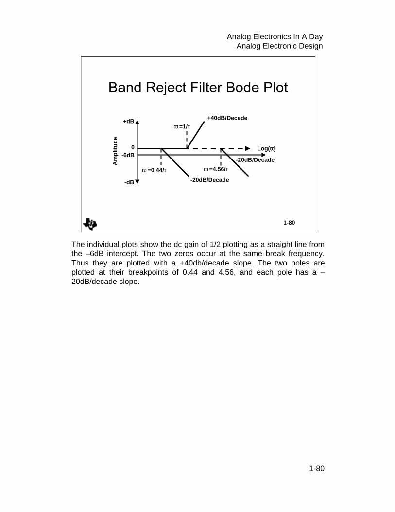
The individual plots show the dc gain of 1/2 plotting as a straight line from the –6dB intercept. The two zeros occur at the same break frequency. Thus they are plotted with a +40db/decade slope. The two poles are plotted at their breakpoints of 0.44 and 4.56, and each pole has a –20dB/decade slope.

1-81
Analog Electronics In A DayAnalog Electronic Design
1-81
0dB
-6dB
+25°
+12°
0.0°Ph
ase
Sh
ift
Am
plit
ud
e
ω=0.44/τ ω=1/τ ω=4.56/τ
-5°
The dc gain causes the amplitude of the combined plot to intercept the axis at -6dB, and it breaks down when it reaches the first pole, ω = 0.44/τ. When the amplitude function gets to the double zero at ω = 1/τ, the first zero cancels out the pole, and the second zero breaks up resulting in a slope of 20dB/decade. The upward slope continues until the second pole cancels out the second zero at ω = 4.56/τ, and the amplitude is flat from that point out in frequency.
When the separation between pole zero combinations is a decade or more in frequency, it is easy to draw the Bode plot because there is little interaction between the poles and/or zeros. As the poles and/or zeros get closer together the plot gets harder to make because their interaction around the break points caused by the closeness magnifies the -3dB breakpoint error. The phase is especially hard to plot because it is a tangent function, but picking a few salient points and sketching them in first gets you a pretty good approximation. The Bode plot enables the designer to get a good idea of pole zero placement, and it is valuable for fast evaluation of possible compensation techniques. When the situation gets critical, accurate calculations must be made and plotted to insure that the plot represents the true situation.

1-82
Analog Electronics In A DayAnalog Electronic Design
1-82
βA1A
VV
I
O
+=
Log(f)
( )βA120Log +
dB
( )A20Log
I
O
VV
20Log
Am
plit
ud
e
Consider this equation:
Taking the log of this equation yields
If A and β do not contain poles or zeros there are no break points. Then the Bode plot is flat, and because there are no poles or zeros to contribute phase shift, the circuit can’t oscillate.
β+=
A1A
VV
IN
OUT
β+= A1 20Log-A20Log )/V20Log(V INOUT

1-83
Analog Electronics In A DayAnalog Electronic Design
1-83
Log(f)
ω3dBω=ωAMP
( )βA120Log + X
dB
( )A20Log
I
O
VV
20Log
βA1A
VV
I
O
+=
AMP
j1
aA
ωω+
=
All real op amps have many poles, and some op amps have little or no internal compensation, so these op amps must be externally compensated to prevent oscillation. A different breed of op amp is internally compensated so that they appear to have a single pole. Beware, these op amps only appear to have a single pole, and at high frequencies they may accumulate as much as 155o phase shift before the gain intercepts the 0dB axis. Such an amplifier would have an approximate equation similar to that given below.
The amplifier gain, A, intercepts the axis at 20Log(A), and it breaks down at a slope of -20dB/decade at ω = ωa. The negative slope continues for all frequencies greater than the breakpoint, ω = ωa. The closed loop circuit gain intercepts the axis at 20Log(VOUT/VIN), and because β does not have any poles or zeros, the closed loop circuit gain is constant until it’s projection intersects the amplifier gain at point X. After intersection with the amplifier gain curve, the closed loop gain follows the amplifier gain because the amplifier becomes the controlling factor.
Actually, the closed loop gain starts to roll off earlier, and it is down 3dB at point X. At point X the difference between the closed loop gain and the amplifier gain is -3dB, thus the term -20Log|1+Aβ| = -3dB. The magnitude of 3dB is , hence and elimination of the radicals shows that Aβ = 1.
a
j1
aA
ωω+
=
2 2)A(1 2 =β+

1-84
Analog Electronics In A DayAnalog Electronic Design
The loop gain transfer function is given below in a form common to many circuits, so it is analyzed in detail.
The quantity, K, is the dc gain, and it plots as a straight line with an intercept of 20Log(K). The two break points, ω = ω1 and ω = ω2, are plotted in the Bode plot. Each breakpoint contributes -20dB/decade slope to the plot, and 45° phase shift resulting from each breakpoint is plotted at the breakpoints.
This transfer function is referred to as a “two slope” because it two breakpoints resulting in a –40dB/decade slope. When a Bode plot crosses the 0dB (loop gain equals one) intercept the two slope indicates that phase shift has accumulated and consequently, the circuit has the ability to oscillate. Notice that a one slope can only accumulate 90° phase shift, so a one slope transfer function can’t oscillate. Furthermore, a two slope system can accumulate 180° phase shift, therefore a transfer function with a two or greater slope is capable of oscillation.
1-84
( )( )s1s1K
A21 ττ
β++
=
where K=DC gain.
-180°φM
Log(f)
-135°
1/τ2-45°
1/τ1
0dB
dB
20Log(K)
GM
20Log(A β)
Ph
ase
(Aβ)
Am
plit
ud
e (A
β)
( )( )s1s1K
A21 τ+τ+
=β

1-85
Analog Electronics In A DayAnalog Electronic Design
A one slope crossing the 0dB intercept is stable, whereas a two or greater slope crossing the 0dB intercept may be stable or unstable depending upon the accumulated phase shift. Two stability terms; the phase margin, φM, and the gain margin, GM, are defined here. Of these two terms the phase margin is much more popular because phase shift is critical for stability. Phase margin is a measure of the difference in the actual phase shift and the theoretical 180° phase shift required for oscillation. Phase margin measurements or calculations are made at the 0dB crossover point. The gain margin is a measure of the difference from the theoretical 0dB required for oscillation, and the gain margin is measured orcalculated at the 180° phase point. Phase margin is expressed mathematically below:
The phase margin is very small, 20°, so it is hard to measure or predict from the Bode plot. A designer probably doesn’t want a 20° phase margin because small phase margins cause the system to overshoot and rings, but this case points out the need to calculate small phase margins carefully. The circuit is stable, and it doesn’t oscillate because the phase margin is positive. Also, the circuit that has the smallest phase margin has the highest frequency response and bandwidth.
( )β−=φ − Agenttan180 1M
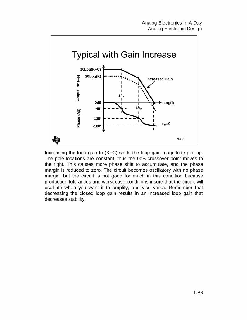
1-86
Analog Electronics In A DayAnalog Electronic Design
1-86
-180°φM=0
Log(f)
-135°
1/τ2-45°
1/τ1
0dB
20Log(K)P
has
e (A
β)A
mp
litu
de
(Aβ) Increased Gain
20Log(K+C)
Increasing the loop gain to (K+C) shifts the loop gain magnitude plot up. The pole locations are constant, thus the 0dB crossover point moves to the right. This causes more phase shift to accumulate, and the phase margin is reduced to zero. The circuit becomes oscillatory with no phase margin, but the circuit is not good for much in this condition because production tolerances and worst case conditions insure that the circuit will oscillate when you want it to amplify, and vice versa. Remember that decreasing the closed loop gain results in an increased loop gain that decreases stability.
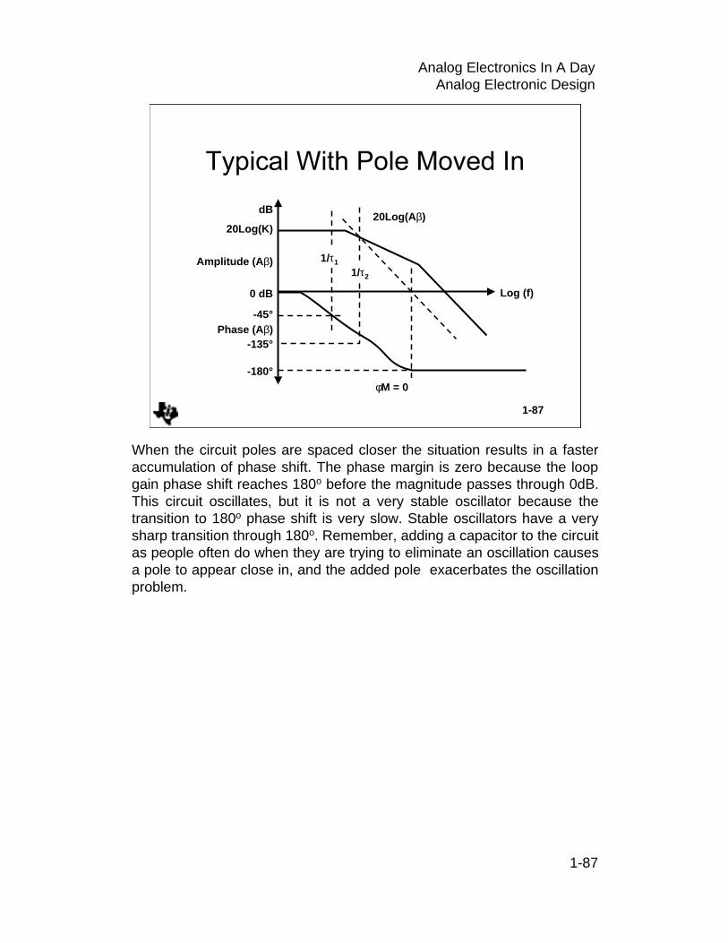
1-87
Analog Electronics In A DayAnalog Electronic Design
1-87
dB
20Log(K)
Amplitude (Aβ)
0 dB
-45°Phase (A β)
-135°
-180°φM = 0
Log (f)
20Log(A β)
1/τ1
1/τ2
When the circuit poles are spaced closer the situation results in a faster accumulation of phase shift. The phase margin is zero because the loop gain phase shift reaches 180o before the magnitude passes through 0dB. This circuit oscillates, but it is not a very stable oscillator because the transition to 180o phase shift is very slow. Stable oscillators have a very sharp transition through 180o. Remember, adding a capacitor to the circuit as people often do when they are trying to eliminate an oscillation causes a pole to appear close in, and the added pole exacerbates the oscillation problem.

1-88
Analog Electronics In A DayAnalog Electronic Design
1-88
PeakingOvershoot
Ringing

1-89
Analog Electronics In A DayAnalog Electronic Design
1-89
FEEDBACK SYSTEM BLOCK DIAGRAM
A
β
VOUT
EΣVIN
-
( )
1Afor/1V/V
A1A
VV
VVA1/A
VVA/V
VVE
EAV
INOUT
IN
OUT
INOUT
OUTINOUT
OI
O
>>ββ=β+
=
=β+β−=
β−==
The block “A” is called the direct gain, and the block “β” is called the feedback factor. All feedback systems can be represented by this basic diagram because complicated diagrams can be reduced to this simple diagram.
The output and error equations are written below.
(7-89-1
(7-89-2
Combining equations 7-89-1 and 7-89-2 yields equation 7-89-3.
(7-89-3
Collecting terms yields equation 7-89-4.
(7-89-4
Rearranging terms yields the classic form of the feedback equation.
(7-89-5
Please notice that equation 7-89-5 reduces to equation 7-89-6 when the term , Aβ, in equation 7-89-5 becomes very large with respect to one. Equation 7-89-6 is called the ideal feedback equation because it depends on the assumption that Aβ >>1, and it finds extensive use when amplifiers are assumed to have ideal qualities. Under the conditions that Aβ >>1, the system gain is determined by the feedback factor β. Stable passive circuit components are used to implement the feedback factor, thus the ideal closed loop gain is predictable and stable because β is stable and predictable.
(7-89-6
EAVOUT =
OUTIN VVE β−=
OUTINOUT VVA
Vβ−=
INOUT VA1
V =
β+
β+=
A1A
VV
IN
OUY
β= 1
VV
IN
OUT

1-90
Analog Electronics In A DayAnalog Electronic Design
1-90
Block Diagram For Computing The Loop Gain
A
β
VTOΣ VTI
-
180 /1A
0A1
−=−=β
=β+
1
β= AV/V TITO
The quantity Aβ is so important that it has been given a special name, loop gain. Consider the figure; when the voltage inputs are grounded (current inputs are opened) and the loop is broken the calculated gain is the loop gain, Aβ. Now, keep in mind that this is a mathematics of complex numbers which have magnitude and direction. When the loop gain approaches minus one, or to express it mathematically 1∠180o, equation 7-1-5 approaches infinity because 1/0⇒∝. The circuit output heads for infinity as fast as it can using the equation of a straight line. If the output were not energy limited the circuit would explode the world, but it is energy limited by the power supplies so the world stays intact.
Active devices in electronic circuits exhibit non-linear behavior when their output approaches a power supply rail, and the non-linearity reduces the amplifier gain until the loop gain no longer equals 1∠180o. Now the circuit can do two things: first it could become stable at the power supply limit, or second, it can reverse direction (because stored charge keeps the output voltage changing) and head for the negative power supply rail.
The first state where the circuit becomes stable at a power supply limit is named lockup; the circuit will remain in the locked up state until power is removed. The second state where the circuit bounces between power supply limits is named oscillatory. Remember, the loop gain, Aβ, is the sole factor that determines stability for a circuit or system. Inputs are grounded or disconnected when the loop gain is calculated, so they have no affect on stability.
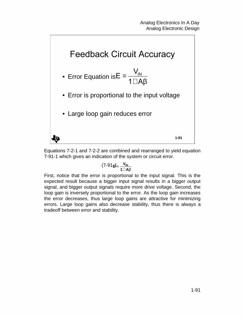
1-91
Analog Electronics In A DayAnalog Electronic Design
1-91
• Error Equation is
• Error is proportional to the input voltage
• Large loop gain reduces error
β+= IN
Equations 7-2-1 and 7-2-2 are combined and rearranged to yield equation 7-91-1 which gives an indication of the system or circuit error.
(7-91-1
First, notice that the error is proportional to the input signal. This is the expected result because a bigger input signal results in a bigger output signal, and bigger output signals require more drive voltage. Second, the loop gain is inversely proportional to the error. As the loop gain increases the error decreases, thus large loop gains are attractive for minimizing errors. Large loop gains also decrease stability, thus there is always a tradeoff between error and stability.
β+=
A1V
E IN

1-92
Analog Electronics In A DayAnalog Electronic Design
1-92
VIN
ZG
VA
ZF
-+
a VOUT
VB
( )
FG
GIN
OUT
FG
TOUGINOUT
GF
GOUTB
BINOUT
ZZaZ
1
aV
V
ZZVaZ
aVV
ZZZV
V
VVaV
++
=
+−=
+=
−=
Equation 7-92-1 is the amplifier transfer equation.
(7-92-1
Equation 7-92-2 is the output equation.
for IB = 0 (7-92-2
Combining equations 7-92-1 and 7-92-2 yields equation 7-92-3.
(7-92-3
Rearranging terms in equation 7-92-3 yields equation 7-92-4 which describes the transfer function of the circuit.
(7-92-4
( )BINOUT VVaV −=
GF
GOUTB ZZ
ZVV
+=
FG
OUTGINOUT ZZ
VaZaVV
+−=
FG
GIN
OUT
ZZaZ
1
aV
V
++
=

1-93
Analog Electronics In A DayAnalog Electronic Design
1-93
a
ZG/(ZG+ZF)
VOUTΣVIN
-
Equation 7-5-4 can be expressed as the block diagram. The block diagram makes it easy to relate the stability of the non-inverting op amp to the general stability equation already developed.

1-94
Analog Electronics In A DayAnalog Electronic Design
1-94
VTI ZG
ZF-
+a
VTO
aVTI
β=+
= AZZ
aZVV
FG
G
TI
TO
The non-inverting loop gain is calculated by breaking the loop and applying a test signal, VTI. First, voltage sources are grounded and current sources are open circuited. The return signal, VTO, is calculate first and then the loop gain is calculated as shown in the figure. The loop gain determines stability. The op amp inputs have no effect on stability because they are grounded or open circuited for the loop gain calculation.
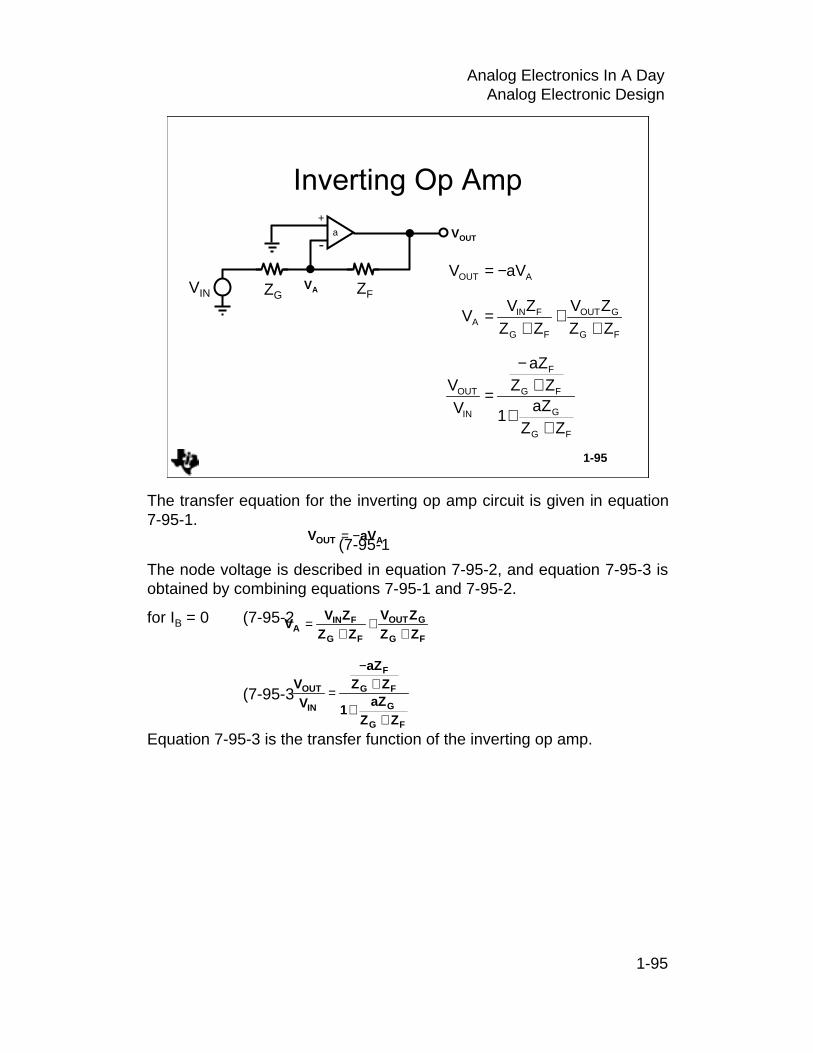
1-95
Analog Electronics In A DayAnalog Electronic Design
1-95
VIN ZG ZF
-
+a VOUT
VA
FG
G
FG
F
IN
OUT
FG
GOUT
FG
FINA
AOUT
ZZaZ
1
ZZaZ
VV
ZZZV
ZZZV
V
aVV
++
+−
=
++
+=
−=
The transfer equation for the inverting op amp circuit is given in equation 7-95-1.
(7-95-1
The node voltage is described in equation 7-95-2, and equation 7-95-3 is obtained by combining equations 7-95-1 and 7-95-2.
for IB = 0 (7-95-2
(7-95-3
Equation 7-95-3 is the transfer function of the inverting op amp.
AOUT aVV −=
FG
GOUT
FG
FINA ZZ
ZVZZ
ZVV
++
+=
FG
G
FG
F
IN
OUT
ZZaZ
1
ZZaZ
VV
++
+−
=

1-96
Analog Electronics In A DayAnalog Electronic Design
1-96
a
ZG/ZF
VOUTΣVIN
-
ZF/(ZG+ZG)+
VA
Equation 7-8-3 can be expressed as the block diagram. The block diagram makes it easy to relate the stability of the inverting op amp to the general stability equation already developed.

1-97
Analog Electronics In A DayAnalog Electronic Design
1-97
FG
G
FG
F
IN
OUT
FG
GIN
OUT
ZZaZ
1
ZZaZ
VV
ZZaZ
1
aV
V
++
+−
=
++
=• Non-Inverting
• Inverting

1-98
Analog Electronics In A DayAnalog Electronic Design
1-98
• Loop Gain
• AINV ≠ ANON-INV
• Inputs have no affect on stability
• Error is inversely proportional to loop gain
FG
G
ZZaZ
A+
=β
There are several things that must be mentioned at this point in the analysis. First, the transfer functions for the non-inverting and inverting equations, 7-5-4 and 7-8-3, are different. For a common set of ZG and ZFvalues the magnitude and polarity of the gains are different. Second, the loop gain of both circuits, as shown in equations 7-5-4 and 7-8-3, is identical. Thus, the stability performance of both circuits is identical even though their transfer equations are different. This makes the important point that stability is not dependent on the circuit inputs. Third, the “A” gain block shown in figure 7-2-1 is different for each op amp circuit. By comparison of equations 7-5-4 and 7-8-3 we see that ANON-INV = a and AINV = aZF/(ZG + ZF). The error is inversely proportional to the loop gain; thus, the accuracy of identical closed loop gain inverting and non-inverting op amp circuits is different.
(7-98-1
Equation 7-98-1 is used to compensate all op amp circuits.FG
G
ZZaZ
A+
=β
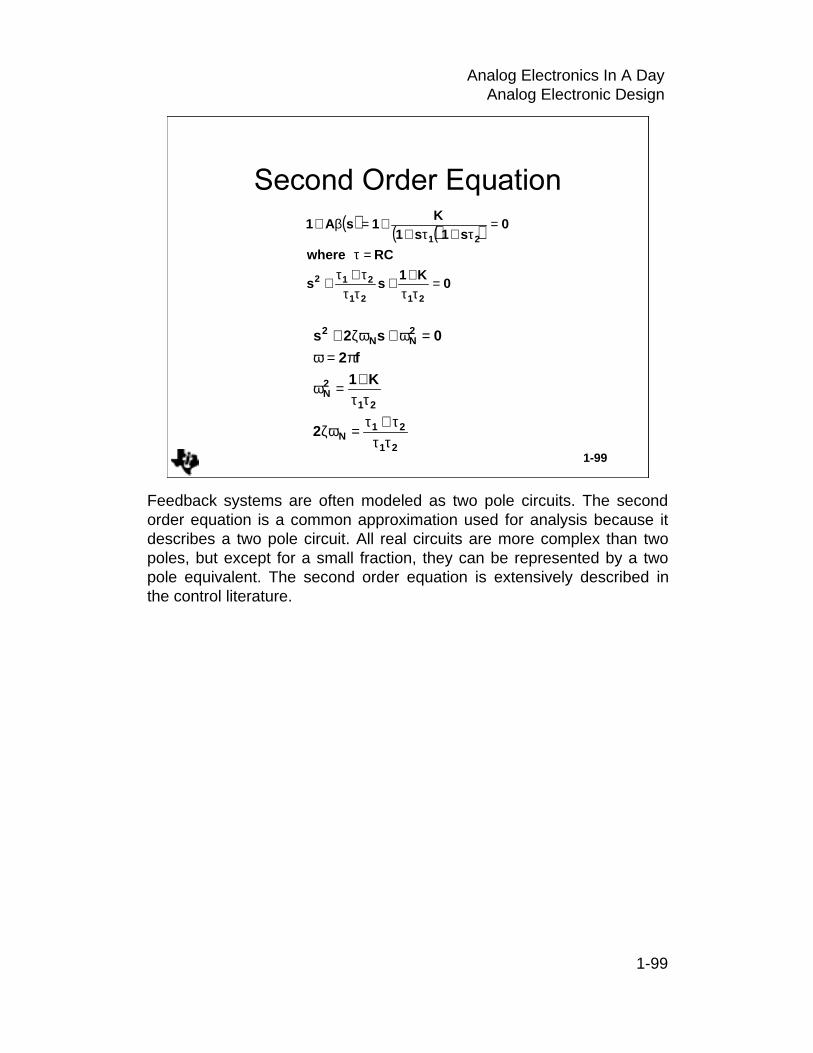
1-99
Analog Electronics In A DayAnalog Electronic Design
1-99
( ) ( )( )
0K1
ss
RCwhere
0s1s1
K1sA1
2121
212
21
=ττ
++ττ
τ+τ+
=τ
=τ+τ+
+=β+
21
21N
21
2N
2NN
2
2
K1
f2
0s2s
τττ+τ
=ζω
ττ+=ω
π=ω=ω+ζω+
Feedback systems are often modeled as two pole circuits. The second order equation is a common approximation used for analysis because it describes a two pole circuit. All real circuits are more complex than two poles, but except for a small fraction, they can be represented by a two pole equivalent. The second order equation is extensively described in the control literature.

1-100
Analog Electronics In A DayAnalog Electronic Design
1-100
( ) ( )
( )
CN1
M
212
C
21C1M
4N
2C
2N
4C
22
2C
21
2C
/2TAN
1TAN
02
111
K
ωζω=φ
ττω−τ+τω=φ
=ω−ωζω+ω
=τω+τω+
−
−
The magnitude and phase of a second order equation is shown above.

1-101
Analog Electronics In A DayAnalog Electronic Design
1-101
Dam
pin
g R
atio
, ζ
0 10 20 30 40 50 60 70 800
0.2
0.4
0.6
0.8
1.0
Percent Maximum Overshoot
Phase Margin, φM
The phase margin, and overshoot are plotted versus the damping ratio. Enter the graph at the calculated damping ratio, say 0.4, and read the overshoot at 25% and the phase margin at 42o. If a designer had a circuit specification of 5% overshoot, then the damping ratio must be 0.78 with a phase margin of 62o.

1-102
Analog Electronics In A DayAnalog Electronic Design
1-102
Input
Overshoot
Output
Input
Ringing
Output
As the phase margin decreases zeta decreases and the circuit tends towards instability. First, the circuit exhibits overshoot where the response overshoots the expected output value. Second, the circuit exhibits ringing where the response oscillates (decaying oscillation) above and below the expected output value. Third, oscillation which is ringing with no decay, results.

1-103
Analog Electronics In A DayAnalog Electronic Design
1-103
Design
Analysis
Calculations ResultsCompareResults & Calculations
SpecificationLeads toDesign Criteria
SelectCriticalComponents
CircuitConfiguration
The design procedure starts with the specification. The designer creates an error budget based on the specifications. The most critical components (converters, DSP, etc.) are selected first, and their errors are subtracted from the error budget. The least critical components (op amps, interface, etc) are selected next, and their tolerance is selected to be within the error budget.
The circuit configuration has always been in mind when the components were selected, and now the circuit configuration is modified to accommodate the selected components. Analysis, which consists ofcalculations and results/specification verification, comes last.

1-104
Analog Electronics In A DayAnalog Electronic Design
1-104
• Worry about stray capacitance
• Amplifier must have enough bandwidth
• Terminations must be considered
• Low frequency assumptions start to break down
• Secondary effects start to take charge
At high frequencies the assumption of high gain breaks down rapidly. This leads to excess phase shift and the possibility of instability. Stray components such as capacitance and inductance become critical components which must be neutralized or accounted for.

1-105
Analog Electronics In A DayAnalog Electronic Design

1-106
Analog Electronics In A DayAnalog Electronic Design
1-106
Voltage feedback amplifiers (VFA) have been with us for about 60 years, and they have been a problem for circuit designers since the first day. You see, the feedback that makes them versatile and accurate also has a tendency to make them unstable. The operational amplifier (op amp) circuit configuration uses a high gain amplifier whose parameters are determined by external feedback components. The amplifier gain is so high that the slightest input signal would saturate the amplifier output without these external feedback components. The op amp is in common usage, so this configuration is examined in detail, but the results are applicable to many other voltage feedback circuits. Current feedback amplifiers (CFA) are similar to VFAs, but the differences are important enough to warrant CFAs being handled in a separate application note.
Feedback circuits exhibit poor phase response, overshoot, and ringing long before oscillation occurs, and these effects are consideredundesirable by circuit designers. Relative stability is defined in terms of performance. By definition, when designers decide what tradeoffs are acceptable they determine what the relative stability of the circuit is. A relative stability measurement is the damping ratio, ζ. The damping ratio is related to phase margin, hence phase margin is another measure of relative stability.

1-107
Analog Electronics In A DayAnalog Electronic Design
1-107
• Transistors have poor drift stability• Transistors have wide initial tolerances
on current gain• Op amps are built with transistors• Feedback makes op amp stability and
initial tolerance dependent on external passive components
Amplifiers are built with active components such as transistors. Pertinent transistor parameters like transistor gain are subject to drift and initial inaccuracies from many sources, so amplifiers being built from these components are subject to drift and inaccuracies. The drift and inaccuracy is minimized or eliminated by using negative feedback. The op amp circuit configuration employs feedback to make the transfer equation of the circuit independent of the amplifier parameters (well almost), and while doing this, the circuit transfer function is made dependent on external passive components. The external passive components can be purchased to meet almost any drift or accuracy specification; only the cost and size of the passive components limit their use.
Once feedback is applied to the op amp it is possible for op amp circuit to become unstable. Certain amplifiers belong to a family called internally compensated op amps; they contain internal capacitors which are sometimes advertised as precluding instabilities. Although internally compensated op amps do not oscillate when operated under specified conditions, many have relative stability problems that manifest themselves as poor phase response, ringing and overshoot. The only absolutely stable internally compensated op amp is the one lying on the workbench without power applied! All other internally compensated op amps oscillate under some external circuit conditions.

1-108
Analog Electronics In A DayAnalog Electronic Design
1-108
• Some op amps have internal compensation• Internally compensated op amps may be
unstable under some circuit conditions• Circuit parasitic components cause instability• Compensation is selected to stabilize the
circuit• Compensation does not extend op amp
bandwidth
Non-internally compensated or “externally” compensated op amps are unstable without the addition of external stabilizing components. This situation is a disadvantage in many cases because they require additional components, but the lack of internal compensation enables the top drawer circuit designer to squeeze the last drop of performance from the op amp. You have two options: op amps internally compensated by the IC manufacturer, or externally compensated by you. Compensation, except that done by the op amp manufacturer, must be done external to the IC. Surprisingly enough, internally compensated op amps require external compensation for demanding applications.Compensation is achieved by adding external components that modify the circuit transfer function so that it becomes unconditionally stable. There are several different methods of compensating an op amp, and as you might suspect, there are pros and cons associated with each method of compensation. Teaching you how to compensate and how to evaluate the results of compensation is the intent of this seminar. After the op amp circuit is compensated, it must be analyzed to determine the effects of compensation. The modifications that compensation have on the closed loop transfer function often determine which compensation scheme is most profitably employed.First we determine what compensation method to use. Second, we derive the compensation equations. Third, we analyze the closed loop transfer function to determine how it is modified by the compensation. The effect of the compensation on the closed loop transfer function often determines which compensation technique will be used.

1-109
Analog Electronics In A DayAnalog Electronic Design
1-109
VCC
RC
C
VIN
RB
I
VEE
Op amps are internally compensated to save external components and to enable their use by less knowledgeable people. It takes some measure of analog knowledge to compensate an analog circuit. Internally compensated op amps normally are stable when they are used in accordance with the applications instructions. Internally compensated op amps are not unconditionally stable. They are multiple pole systems, but they are internally compensated such that they appear as a single pole system over much of the frequency range. There is no such thing as free lunch because internal compensation severely decreases the closed loop bandwidth of the op amp.
Internal compensation is accomplished in several ways, but the most common method is to connect a capacitor across the collector-base junction of a common-emitter voltage amplifier. The Miller effect multiplies the capacitor value by an amount approximately equal to the stage gain, thus the Miller effect uses small value capacitors for compensation.

1-110
Analog Electronics In A DayAnalog Electronic Design
1-110
Large-signal Differential Voltage Amplification And Phase Margin Vs Frequency
100
80
60
40
20
0
-20
-401k 10k 100k 1M 10M
f — Frequency — Hz
AV
D—
Larg
e S
igna
l Diff
eren
tial A
mpl
ifica
tion
—dB
φM —
Pha
se M
argi
n —
degr
ees
120
180
240
300
60
0
-90
-60
VDD = 5 VRL = 600 ΩCL = 600 pFTA = 25°CAVD
Phase
Internally compensated op amps can’t be modeled as unconditionally stable single pole circuits because they all have multiple poles. The TLV277X series of op amps are shown in this and the next 3 slides. At VCC = 5V, the phase margin at the 0dB crossover point is 60o, while it is 30o at VCC = 2.7V. This translates to an expected overshoot of 18% at VCC= 5V and 28% at VCC = 2.7V. Unfortunately the time response plots are done with 100pF loading capacitance, hence we can’t check our figures very well. The VCC = 2.7V overshoot is approximately 2%, and it is almost impossible to figure out what the overshoot would have been with a 600pF loading capacitor. The small signal pulse response is done with mV signals, and that is a more realistic measurement than using the full signal swing.

1-111
Analog Electronics In A DayAnalog Electronic Design
1-111
Large-signal Differential Voltage Amplification And Phase Margin Vs Frequency100
80
60
40
20
0
-20
-401k 10k 100k 1M 10M
f — Frequency — Hz
AV
D—
Larg
e S
igna
l Diff
eren
tial A
mpl
ifica
tion
—dB
φM —
Pha
se M
argi
n —
degr
ees
120
180
240
300
60
0
-90
-60
VDD= 2.7 VRL = 600 ΩCL = 600 pFTA = 25°C

1-112
Analog Electronics In A DayAnalog Electronic Design
1-112
Voltage-Follower Small-Signal Pulse Response
100
80
60
0
40
20
-20
-40
-600 0.5 1.5 2.5 3.5 4.51 2 3 4 5
VO
—O
utpu
t Vol
tage
—m
VVDD = 2.7 VRL = 600ΩCL = 100 pFAV = 1TA = 25°C
1 — Time — µs
Internally compensated op amps are very desirable because they are easy to use, and they don’t require external compensation components. Their drawback is that the bandwidth is limited by the internal compensation scheme. The error in an op amp circuit is determined by the op amp open loop gain. In a non-inverting buffer configuration, the TL277X is limited to 1% error at 50kHz (VCC = 2.7V) because the op amp gain is 40dB at that point. Circuit designers can play cute tricks such as bypassing the op amp with a capacitor to emphasize the high frequency gain, but the error is still 1%. If the TLV277X were not internally compensated, it could be externally compensated for a lower error at 50kHz because the gain would be much higher.

1-113
Analog Electronics In A DayAnalog Electronic Design
1-113
Inverting Small-Signal Pulse Response
100
80
60
0
40
20
-20
-40
-600 0.5 1.5 2.5 3.5 4.51 2 3 4 5
VO
—O
utpu
t Vol
tage
—m
VVDD = 2.7 VRL = 600ΩCL = 100 pFAV = -1TA = 25°C
1 — Time — µs

1-114
Analog Electronics In A DayAnalog Electronic Design
1-114
VOUT
CLZF
ZG
ZO∆Va
VIN
∆V
Point x
Capacitive loading causes potential instabilities, thus an op amp loaded with an output capacitor is a circuit configuration that must be analyzed. This circuit is called dominant pole compensation because if the pole formed by the op amp output impedance and the loading capacitor is located close to the zero frequency axis it becomes dominant.

1-115
Analog Electronics In A DayAnalog Electronic Design
1-115
β
( )1
ZZZsCZ ZZ
ZZZaZ
AV
V
1sCZZ
Z
1sCZVa
V
OGF
LOOF
OGF
G
TEST
RETURN
LO
OTH
LOTH
+++
+++=β=
+=
+∆=
VTEST = ∆Va
VRETURN
ZG
ZFZOCL
VOUT
The analysis starts by looking into the capacitor and taking the Thevenin equivalent circuit.
(8-115-1 (8-115-2
Then the loop gain equation is written.
(8-115-3
When the assumption is made that (ZF + ZG) >> ZO equation 8-115-3 reduces to equation 8-115-4.
(8-115-4Equation 8-10-5 models the op amp as a second order system, hence substituting the second order model for a in equation 8-10-4 yields equation 8-10-6 which is the stability equation for the dominant pole compensation circuit.
(8-115-5 (8-115-6
Several conclusions can be drawn from equation 8-10-6 depending on the location of the poles. When the pole introduced by ZO and CL moves towards the zero frequency axis it comes close to the τ2 pole, and it adds phase shift to the system. Increased phase shift increases peaking and decreases stability. In the real world many loads, especially cables, are capacitive, and an op amp like the one pictured in figure 8-9 may ring while driving a capacitive load. The load capacitance causes peaking and instability in internally compensated op amps when the op amps do not have enough phase margin to allow for the phase shift introduced by the load.
1sCZVa
VLO
TH +∆=
1sCZZ
ZLO
OTH +
=
( )1
ZZZsCZ ZZ
ZZZaZ
AV
V
OGF
LOGF
OGF
G
TEST
RETURN
+++
+++=β=
++
=β1sCZ
1ZZ
aZA
LOGF
G
( )( )21 ssK
aτ+τ+
= ( )( ) 1sCZ1
ZZZ
ssK
ALOGF
G
21 ++τ+τ+=β

1-116
Analog Electronics In A DayAnalog Electronic Design
1-116
0dB
20Log(Aβ)
dB
1/τ1
Log(f)
1/τ2
Dominant PoleωD
Prior to compensation, the Bode plot of an uncompensated op amp looks like that shown in figure 8-11. Notice that the break points are located close together thus accumulating about 180o of phase shift before the 0dB crossover point; the op amp is not usable and probably unstable. Dominant pole compensation is often used to stabilize these op amps. If a dominant pole, in this case ωD, is properly placed it rolls off the gain so that τ1 introduces 45o phase at the 0dB crossover point. After the dominant pole is introduced the op amp is stable with 45o phase margin, but the op amp gain is drastically reduced for frequencies above ωD. This procedure works well for internally compensated op amps, but is seldom used for externally compensated op amps because inexpensive discrete capacitors are readily available.
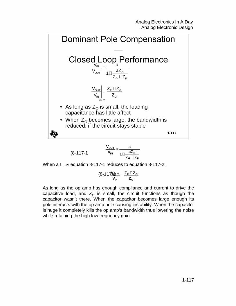
1-117
Analog Electronics In A DayAnalog Electronic Design
1-117
• As long as ZO is small, the loading capacitance has little affect
• When ZO becomes large, the bandwidth is reduced, if the circuit stays stable
G
GF
aIN
OUT
FG
GOUT
IN
ZZZ
VV
ZZaZ
1
aVV
+=
++
=
∞⇒
(8-117-1
When a ⇒ ∞ equation 8-117-1 reduces to equation 8-117-2.
(8-117-2
As long as the op amp has enough compliance and current to drive the capacitive load, and ZO is small, the circuit functions as though the capacitor wasn’t there. When the capacitor becomes large enough its pole interacts with the op amp pole causing instability. When the capacitor is huge it completely kills the op amp’s bandwidth thus lowering the noise while retaining the high low frequency gain.
FG
GIN
OUT
ZZaZ
1
aV
V
++
=
G
GF
IN
OUT
ZZZ
VV +
=

1-118
Analog Electronics In A DayAnalog Electronic Design
1-118
0dB
20Log(Aβ)
dB
1/τ1
Log(f)
1/τ2
Loop Gain Curve
+ GF
G
ZZKZ
20Log
Compensated Loop Gain Curve
-14dB
The original loop gain curve for a closed loop gain of one is shown in figure 8-118, and it is or comes very close to being unstable. If the closedloop non-inverting gain is changed to 9, then K changes from K/2 to K/10.The loop gain intercept on the Bode plot moves down 14dB, and the circuit is stabilized.
Gain compensation works for inverting or non-inverting op amp circuits because the loop gain equation contains the closed loop gain parameters in both cases. When the closed loop gain is increased, the accuracy and the bandwidth decrease. As long as the application can stand the higher gain, gain compensation is the best type of compensation to use.Uncompensated versions of internally compensated op amps are offered for sale as internally compensated op amps with minimum gain restrictions. As long as the circuit gain exceeds the specified gain this is economical and a safe mode of operation.
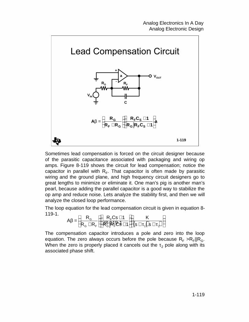
1-119
Analog Electronics In A DayAnalog Electronic Design
1-119
a VOUT
-
+
C
RFRG
VIN
a1CRR
1CRRR
RA
SFG
SF
GF
G
+
+
+
=β
Sometimes lead compensation is forced on the circuit designer because of the parasitic capacitance associated with packaging and wiring op amps. Figure 8-119 shows the circuit for lead compensation; notice the capacitor in parallel with RF. That capacitor is often made by parasitic wiring and the ground plane, and high frequency circuit designers go to great lengths to minimize or eliminate it. One man’s pig is another man’s pearl, because adding the parallel capacitor is a good way to stabilize the op amp and reduce noise. Lets analyze the stability first, and then we will analyze the closed loop performance.
The loop equation for the lead compensation circuit is given in equation 8-119-1.
(8-119-1
The compensation capacitor introduces a pole and zero into the loop equation. The zero always occurs before the pole because RF >RF||RG. When the zero is properly placed it cancels out the τ2 pole along with its associated phase shift.
( )( )
τ+τ+
+
+
+
=β21FG
F
FG
G
ssK
1CsRR1CsR
RRR
A

1-120
Analog Electronics In A DayAnalog Electronic Design
1-120
0dB
20Log(Aβ)
dB
1/τ1
Log(f)
1/τ2
Original Transfer Function20
Lo
g(K
RG/(
RG+R
F))
1/RFC 1/RF||RGC
Modified Transfer Function
The original transfer function is shown in figure 8-120 drawn in solid lines. When the RFC zero is placed at ω = 1/τ2, it cancels out the τ2 pole causing the bode plot to continue on a slope of -20dB/decade. When the frequency gets to ω = 1/(RF||RG)C, this pole changes the slope to -40dB/decade. Properly placed, the capacitor aids stability.

1-121
Analog Electronics In A DayAnalog Electronic Design
1-121
0dB
20Loga
1/τ11/τ2 and
Op Amp Gain
1/RFC
1/RF||RGC
Aβ
FG
F
ZZaZ
20Log+
G
F
ZZ
20Log Ideal Closed Loop Gain
What does it do to the closed loop transfer function? The equation for the inverting op amp closed loop gain is repeated below.
(8-121-1
When a approaches infinity equation 8-121-1 reduces to equation 8-121-2.
(8-121-2
Substituting RF for ZF and RG for ZG in equation 8-121-2 yields equation 8-121-3 which is the ideal closed loop gain equation for the lead compensation circuit. (8-121-3
The forward gain for the inverting amplifier is given in equation 8-121-4.
(8-121-4
The forward gain for the inverting op amp is not the op amp gain. Notice that the forward gain is reduced by the factor RF/(RG +RF), and it contains a high frequency pole. The ideal closed loop gain follows the ideal curve until the 1/RFC breakpoint (same location as 1/τ2 breakpoint), and then it slopes down at -20dB/decade. Lead compensation sacrifices the bandwidth between the 1/RFC breakpoint and the forward gain curve. The location of the 1/RFC pole determines the bandwidth sacrifice, and it can be much greater than shown here. The pole caused by RF, RG, and C does not appear until the op amp’s gain has crossed the 0dB axis, thus it doesn’t affect the ideal closed loop transfer function.
FG
G
FG
F
IN
OUT
ZZaZ
1
ZZaZ
VV
++
+−
=
IN
F
IN
OUT
ZZ
VV
−=
+
−=1CsR
1RR
VV
FG
F
IN
OUT
+
+
=+
=1CsRR
1RR
RZZ
aZA
GFFG
F
FG
F

1-122
Analog Electronics In A DayAnalog Electronic Design
1-122
0dB
20Log(a)
1/τ11/τ2
1/RFC
1/RF||RGC
G
GF
ZZZ
20Log+
Log(f)
The forward gain for the non-inverting op amp is a.
(8-122-1
The plot of the non-inverting op amp with lead compensation is shown in figure 8-122. There is only one plot for both the op amp gain, a, and the forward gain, A, because they are identical in the non-inverting circuit configuration. The ideal starts out as a flat line. But, it slopes down because its closed loop gain contains a pole and a zero. The pole always occurs closer to the low frequency axis because RF > RF||RG. The zero flattens the ideal closed loop gain curve, but it never does any good because it can’t fall on the pole. The pole causes a loss in the closed loop bandwidth by the amount separating the closed loop and forward gain curves.
Although the forward gain is different in the inverting and non-inverting circuits, the closed loop transfer functions take very similar shapes. This becomes truer as the closed loop gain increases because the non-inverting forward gain approaches the op amp gain. This relationship can’t be relied on in every situation, and each circuit must be checked to determine the closed loop effects of the compensation scheme.
+
+
+=
+=
1CsR
1CsRR
RRR
ZZZ
VV
F
GF
G
GF
G
GF
IN
OUT

1-123
Analog Electronics In A DayAnalog Electronic Design
1-123
a VOUT
-
+
CG
RFRG
VIN
( )( )
+τ+τ
+
+
=β1s1s
K1sCRR
1RR
RA
21GFGFG
G
Stray capacitance on op amp inputs is a problem that circuit designers are always trying to get away from because it decreases closed loop frequency response or causes peaking. The circuit shown in figure 8-123has some stray capacitance, CG, connected from the inverting input to ground. Equation 8-123-1 is the loop gain equation for the circuit with input capacitance.
(8-123-1
Op amps having high input and feedback resistors are subject to instability caused by stray capacitance on the inverting input. When the 1/(RF||RGCG) pole moves close to τ2 the stage is set for instability. Reasonable component values for a CMOS op amp are RF = 1MΩ, RG= 1MΩ, and CG = 10pF. The resulting pole occurs at 318kHz, and this frequency is lower than the breakpoint of τ2 for many op amps. There is 90o phase shift resulting from τ1, the 1/ (RF||RGC) pole adds 45o phase shift at 318kHz, and τ2 starts adds another 45o phase shift at about 600kHz. This circuit is unstable because of the stray input capacitance.
( )( )
+τ+τ
+
+
=β1s1s
K1sCRR
1RR
RA
21GFGFG
G

1-124
Analog Electronics In A DayAnalog Electronic Design
1-124
a VOUT
-
+
CG
RFRG
VIN
CF
a
1sCRR
1sCRR
1sCRR
A
FF
F
GG
G
GG
G
++
+
+=β
The circuit is compensated by adding a feedback capacitor as shown in figure 8-124.
(8-124-1
If RGCG = RFCF equation 8-124-1 reduces to equation 8-124-2.
(8-124-2
( )( )
+τ+τ
++
+
+=β1s1s
K
1sCRR
1sCRR
1sCRR
A21
FF
F
GG
G
GG
G
( )( )
+τ+τ
+
=β1s1s
KRR
RA
21FG
G

1-125
Analog Electronics In A DayAnalog Electronic Design
1-125
0dB1/τ1
1/τ2
1/RF||RGCG
Log(f)
20L
og
(Aβ) dB
Ph
ase
(Aβ)
Without CF
With CF
-45
-135
-100
Without CF
With CF
The compensated attenuator Bode plot is shown in figure 8-125. Adding the correct 1/RFCF breakpoint cancels out the 1/RGCG breakpoint, the loop gain is independent of the capacitors. Now is the time to take advantage of stray capacitance. CF can be formed by running a wide copper strip from the output of the op amp over the ground plane under RF; do not connect the other end of this copper strip. The circuit is tuned by removing some copper (a razor works well) until all peaking is eliminated. Then measure the copper, and have an identical trace put on the printed circuit board.
The inverting and non-inverting closed loop gain equations are a function of frequency, Equation 8-125-1 is the closed loop gain equation for the inverting op amp. When RFCF = RGCG equation 8-125-1 reduces to equation 8-125-2 which is independent of the breakpoint. This also happens to the non-inverting op amp circuit. This is one of the few occasions when the compensation does not affect the closed loop gain frequency response.
(8-125-1
When RFCF = RGCG VOUT/VIN = -(RF/RG) (8-125-2
1sCRR
1sCRR
VV
GG
G
FF
F
IN
OUT
+
+−=

1-126
Analog Electronics In A DayAnalog Electronic Design
1-126
a VOUT
-
+
RFRGVIN
RC
( )( ) ( )
++
+++
+
++
=1Cs
RRRRRRRR
1RCsRR
R1s1s
KA
FG
FGFGGF
G
21 ττβ
Lead-lag compensation stabilizes the circuit without sacrificing the closed loop gain performance. This type of compensation leads to excellent high frequency performance. The circuit schematic is shown in figure 8-126, and the loop gain is given in equation 8-126-1.
(8-126-1( )( ) ( )( ) 1Cs
RRRRRRRR
1RCsRR
R1s1s
KA
FG
FGFGFG
G
21 ++
+++
++τ+τ=β

1-127
Analog Electronics In A DayAnalog Electronic Design
1-127
0dB
1/τ1 1/τ2
Log(f)
20Log(Aβ) Before Compensation
1/(RC)
( )( ) C
RRRRRRRR
/1GF
GFFG
+++
COMPENSATION NETWORK
20Log(sRG/(RF+RG))
Amplitude
20Log(Aβ)AfterCompensation
A pole is introduced at ω = 1/RC, and this pole reduces the gain 3dB at the breakpoint. When the zero occurs prior to the first op amp pole it cancels out the phase shift caused by the ω = 1/RC pole. The phase shift is completely canceled before the second op amp pole occurs, and the circuit reacts as if the pole was never introduced. But, Aβ is reduced by the 3dB or more, so the loop gain crosses the 0dB axis at a lower frequency. The beauty of lead lag compensation is that the closed loop ideal gain is not affected.
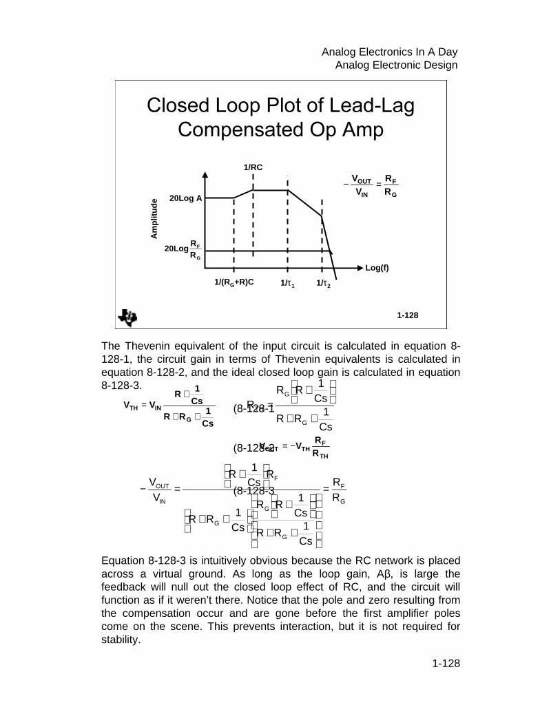
1-128
Analog Electronics In A DayAnalog Electronic Design
1-128
1/τ1
Log(f)
1/τ2
Am
plit
ud
e
1/RC
20Log A
G
F
RR
20Log
1/(RG+R)C
G
F
IN
OUT
RR
VV
=−
The Thevenin equivalent of the input circuit is calculated in equation 8-128-1, the circuit gain in terms of Thevenin equivalents is calculated in equation 8-128-2, and the ideal closed loop gain is calculated in equation 8-128-3.
(8-128-1
(8-128-2
(8-128-3
Equation 8-128-3 is intuitively obvious because the RC network is placed across a virtual ground. As long as the loop gain, Aβ, is large the feedback will null out the closed loop effect of RC, and the circuit will function as if it weren’t there. Notice that the pole and zero resulting from the compensation occur and are gone before the first amplifier poles come on the scene. This prevents interaction, but it is not required for stability.
Cs1
RR
Cs1
RVV
G
INTH++
+=
Cs1
RR
Cs1
RRR
G
G
TH
++
+
=
TH
FTHOUT R
RVV −=
G
F
G
G
G
F
IN
OUT
RR
Cs1
RR
Cs1
RR
Cs1
RR
RCs1
R
VV =
++
+
++
+
=−

1-129
Analog Electronics In A DayAnalog Electronic Design
1-129
• Internally compensated op amps become unstable under certain circuit conditions
• Dominant pole compensation is used in IC design
• Gain compensation is simple but effective
• Stray feedback capacitance stabilizes the circuit
• Stray input capacitance causes instability in high impedance circuits
• Lead-lag compensation emphasizes high frequencies
Internally compensated op amps can, and often do, oscillate under some circuit conditions. Internally compensated op amps need an external pole to get the oscillation or ringing started, and stray capacitances often supply the phase shift required for instability. Loads, such as cables, often cause internally compensated op amps to ring severely.
Dominant pole compensation is often used in IC design because it is easy to implement. It rolls off the closed loop gain early, thus it is seldom used as an external form of compensation unless filtering is required. Load capacitance, depending on its pole location, usually causes the op amp to ring. Large load capacitance can stabilize the op amp because it acts as dominant pole compensation.
The simplest form of compensation is gain compensation. High closed loop gains are reflected in lower loop gains, and in turn, lower loop gains increase stability. If an op amp circuit can be stabilized by increasing the closed loop gain, do it.
Stray capacitance across the feedback resistor tends to stabilize the op amp because it is a form of lead compensation. This compensationscheme is useful for limiting the circuit bandwidth, but it decreases the closed loop gain.
Stray capacitance on the inverting input works with the parallelcombination of the feedback and gain setting resistors to form a pole in the Bode plot, and this pole decreases the circuit’s stability. This effect is

1-130
Analog Electronics In A DayAnalog Electronic Design
normally observed in high impedance circuits built with CMOS op amps. Adding a feedback capacitor forms a compensated attenuator scheme which cancels out the input pole. The cancellation occurs when the input and feedback RC time constants are equal. Under the conditions of equal time constants, the op amp functions as though the stray input capacitance were not there. An excellent method of implementing a compensated attenuator is to build a stray feedback capacitor using the ground plane and a trace off the output node.
Lead-lag compensation stabilizes the op amp, and it yields the best closed loop frequency performance. Contrary to some published opinions, no compensation scheme will increase the bandwidth beyond that of the op amp. Lead-lag compensation gives the best bandwidth for the compensation.
Conclusions
The stability criteria often is not oscillation, rather it is circuit performance as exhibited by peaking

1-131
Analog Electronics In A DayAnalog Electronic Design

1-132
Analog Electronics In A DayAnalog Electronic Design
1-132
Current feedback amplifiers (CFA) have sacrificed the DC precision of voltage feedback amplifiers (VFB) for speed. This tradeoff results in higher bandwidth, faster slew rate, and a bandwidth that is relatively independent of closed loop gain. Although CFAs do not have the precision of their VFB counterparts, they can be DC coupled in video applications without sacrificing much dynamic range. CFAs have eliminated the AC coupling requirement in high frequency amplifiers because they operate in the GHz range while DC coupled. CFAs have much faster slew rates than VFAs, so they have faster rise/fall times and less intermodulation distortion.

1-133
Analog Electronics In A DayAnalog Electronic Design
1-133
VOUTZOUT
G OUTZ(I)
I
GB
ZB
+
-INVERTINGInput
NON-INVERTINGInput
The non-inverting input of a CFA connects to the input of a buffer, so it has a very high impedance similar to a bipolar transistor VFA input. The inverting input connects to the buffer’s output, so the inverting input impedance is very low. ZB models the input buffer’s output impedance which is usually less than 50Ω. The buffer gain, GB, is as close to one as IC design methods can achieve, so it is neglected in the calculations.
The output buffer is used to give the amplifier a low output impedance. Again the gain, GOUT, is very close to one, so it is neglected in this analysis. The impedance of the output buffer can be ignored except when driving very low impedance or capacitive loads. The input buffer’s output impedance can’t be ignored because affects stability at high frequencies. The current-controlled current source, Z, is a transimpedance. Thetransimpedance in a CFA serves the same function as the gain in a VFA. Usually the transimpedance is very high, in the MΩ range, so the CFA gains accuracy in the same manner that the VFA does.

1-134
Analog Electronics In A DayAnalog Electronic Design
1-134
I1Z
VOUT = VTO+
ZF
I2
ZG ZB
I1
VTI
CFA
ZG
ZF
VOUT Becomes VTO; The Test Signal Output
Break Loop Here
Apply Test Signal(VTI) Here
+
-
Stability is independent of the input, and stability depends solely on the loop gain, Aβ. The stability equation is developed by breaking the loop at point “X”, inserting a test signal, VTI, and calculating the return signal VTO. The input buffer gain, the output buffer gain and the output buffer output impedance has been left out of the circuit to simplify calculations. This approximation is valid for almost all applications.

1-135
Analog Electronics In A DayAnalog Electronic Design
1-135
+ZF
I2
ZG ZB
I1
I1Z
VOUT = VTO
VTI
VTO = I1Z
VTI = I2(ZF+ZG||ZB)
I2(ZG||ZB) = I1ZB; For GB = 1
VTI = I1(ZF+ZG||ZB)(1+ZB/ZG)=I1ZF (1+ZB/ZF||ZG)
Aβ = VTO/VTI = Z/(ZF(1+ZB/ZF||ZG))
The transfer equation is given in equation 9-135-1, and the Kirchoff”s law is used to write equations 9-135-2 and 9-135-3.
(9-135-1
(9-135-2
(9-135-3
Equations 9-135-1 and 9-135-2 are combined to yield equation 9-135-4.
(9-135-4
Dividing equation 9-135-1 by equation 9-135-4 yields equation 9-135-5 which is the open loop transfer equation which is commonly known as the loop gain.
(9-135-5
ZIV 1TO =
( )BGF2TI ZZZIV +=
( ) B1BG2 ZIZZI =
( )
+=
++=
GF
BF1
G
BBGF1TI ZZ
Z1ZI
ZZ
1ZZZIV
+
==β
GF
BF
TI
TO
ZZZ
1Z
ZVV
A

1-136
Analog Electronics In A DayAnalog Electronic Design
Equation 9-136-1 is the transfer equation, equation 9-136-2 is the current equation at the inverting node, and equation 9-136-3 is the input loop equation. These equations are combined to yield equation 9-136-4 which is the closed loop gain equation. (9-136-1
(9-136-2
(9-136-3
(9-136-4
When the input buffer impedance, ZB, approaches zero equation 9-136-4 reduces to equation 9-136-5.
(9-136-5
IZVOUT =
−−
=
F
AOUT
G
A
ZVV
ZV
I
BINA IZVV −=
+
+
+
+
=
GF
BF
GF
BF
G
F
IN
OUT
ZZZ
1Z
Z1
ZZZ
1Z
ZZ
1Z
VV
ZZ
1
ZZ
1
ZZ
1
Z
ZZ
1Z
VV
F
G
F
F
F
G
F
IN
OUT
+
+=
+
+
=
1-136
( ) ( )
( )( )
( )GFBF
GFBF
GF
IN
OUT
BINA
FAOUTGA
OUT
ZZ/Z1ZZ
1
ZZ/Z1ZZ/Z1Z
VV
IZVV
Z/VVZ/VI
IZV
++
++
=
==−−=
=
VOUT
G=1IZ
G=1
ZB
+
-
+
I
ZGZF
VA
VIN

1-137
Analog Electronics In A DayAnalog Electronic Design
When the transimpedance, Z, is very high the term ZF/Z in equation 9-5-5 approaches zero, and equation 9-5-5 reduces to equation 9-5-6 which is the ideal closed loop gain equation for the CFA. The ideal closed loop gain equations for the CFA and VFA are identical, and the degree to which they depart from the ideal is dependent on the validity of the assumptions. The VFA has one assumption, that the direct gain is very high, while the CFA has two assumptions, that the transimpedance is very high and that the input buffer impedance is very low. As would be expected, two assumptions are harder to meet than one, thus the CFA departs from the ideal more than the VFA does.
(9-5-6G
F
IN
OUT
ZZ
1V
V +=

1-138
Analog Electronics In A DayAnalog Electronic Design
The inverting CFA configuration is seldom used because the inputimpedance is very low (ZB||ZF +ZG). When ZG is selected as high resistance to swamp out the effects of ZB, ZF must also be high. High values for ZF result in poor bandwidth performance as we will see in the next section. If ZG is selected as a low value, ZB, which is frequency sensitive, causes the gain to increase as frequency increases. These limitations restrict the applications for the inverting CFA.
The current equation for the input node is written as equation 9-138-1. Equation 9-138-2 defines the dummy variable, VA, and equation 9-138-3 is the transfer equation for the CFA. These equations are combined and simplified leading to equation 9-138-4 which is the closed loop gain equation for the inverting CFA. (9-138-1
(9-138-2
(9-138-3
(9-138-4
F
OUTA
G
AIN
ZVV
ZVV
1−=−+
AB VIZ −=
OUTVIZ =
+
+
+
−=
GF
BF
GF
BG
IN
OUT
ZZZ
1Z
Z1
ZZZ
1Z
Z
VV
1-138
VOUT
G=1IZ
G=1
ZB
+
-
+
I
ZG ZF
VA
VIN
( )
( )GFBF
GFBG
IN
OUT
OUT
AB
F
OUTA
G
AIN
ZZ/Z1ZZ
1
ZZ/Z1ZZ
VV
VIZ
VIZ
ZVV
IZ
VV
++
+−=
=
−=
−=+−

1-139
Analog Electronics In A DayAnalog Electronic Design
When ZB approaches zero in equation 9-7-4 it reduces to equation 9-7-5.
(9-7-5
When Z is very large equation 9-7-5 becomes equation 9-7-6 which is the ideal closed lop gain equation for the inverting CFA.
(9-7-6
The ideal closed loop gain equation for the inverting VFA and CFA op amps are identical. Both configurations have lower input impedance than the non-inverting configuration has, but the VFA has one assumption while the CFA has two assumptions. Again, as was the case with the non-inverting counterparts, the CFA is less ideal than the VFA because of the two assumptions. The zero ZB assumption always breaks down in bipolar-junction transistors as is shown later. The differential amplifier configuration is almost never used because of the gross CFA input impedance mismatch.
G
F
IN
OUT
ZZ
VV −=
F
G
IN
OUT
Z1
Z1
Z1
VV
+−=
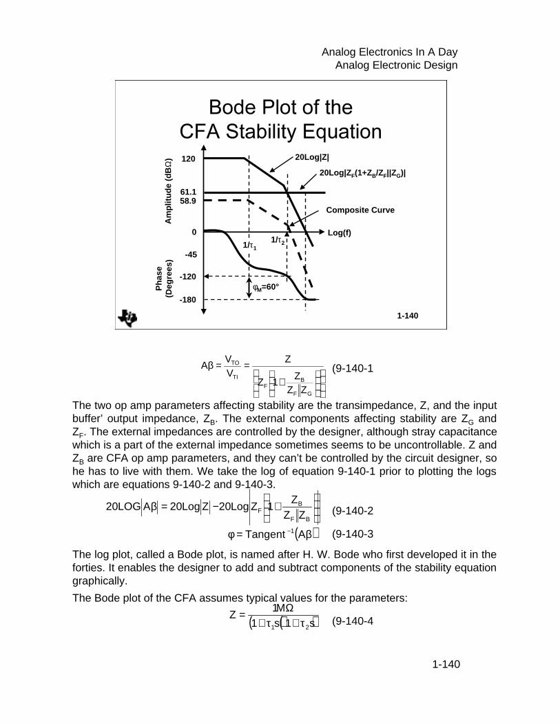
1-140
Analog Electronics In A DayAnalog Electronic Design
1-140
Log(f)0
58.961.1
-180
-120φM=60°
-45
120 20Log|Z|
20Log|Z F(1+ZB/ZF||ZG)|
Composite Curve
1/τ21/τ1
Am
plit
ud
e (d
BΩ
)P
has
e(D
egre
es)
(9-140-1
The two op amp parameters affecting stability are the transimpedance, Z, and the input buffer’ output impedance, ZB. The external components affecting stability are ZG and ZF. The external impedances are controlled by the designer, although stray capacitance which is a part of the external impedance sometimes seems to be uncontrollable. Z and ZB are CFA op amp parameters, and they can’t be controlled by the circuit designer, so he has to live with them. We take the log of equation 9-140-1 prior to plotting the logs which are equations 9-140-2 and 9-140-3.
(9-140-2
(9-140-3
The log plot, called a Bode plot, is named after H. W. Bode who first developed it in the forties. It enables the designer to add and subtract components of the stability equation graphically.
The Bode plot of the CFA assumes typical values for the parameters:
(9-140-4
+
==β
GF
BF
TI
TO
ZZZ
1Z
ZVV
A
+−=β
BF
BF ZZ
Z1ZLog20ZLog20ALOG20
( )β=φ − ATangent 1
( )( )s1s1M1
Z21 τ+τ+
Ω=

1-141
Analog Electronics In A DayAnalog Electronic Design
(9-9-5
(9-9-6
The transimpedance has two poles and the plot shows that the op amp will be unstable without the addition of external components because 20Log|Z| crosses 0dB axis when the phase shift is 180o. The external components reduce the loop gain 61.1dB, so the circuit is stable because it has 60o phase margin. Notice that the parallel combination of ZF and ZGcontribute little to the phase margin because ZB is so small.
When ZB = 0Ω and ZF = RF the loop gain equals Aβ = Z/RF. Under these conditions stability is determined by Z and RF, and a value of RF can always be found to stabilize the circuit. The transimpedance and feedback resistor have a major impact on stability, but the input buffer’s output impedance has a minor effect on stability. Since ZB increases with an increase in frequency, it tends to increase stability at higher frequencies.
Ω= 70ZB
Ω== k1ZZ FG

1-142
Analog Electronics In A DayAnalog Electronic Design
The feedback resistor determines stability and it has an effect on closed loop bandwidth, so it must be selected very carefully. Most CFA IC manufacturers employ applications and product engineers who spend a great deal of time and effort selecting RF. They measure each non-inverting gain with several different feedback resistors to gather data. Then they pick a compromise value of RF which yields stable operation with low peaking, and that value of RF is recommended on the data sheet for that specific gain. Generally this is done for several different gains is anticipation of the various configurations their customers will use.When the circuit designer strays from the RF value recommended on the data sheet they get into stability problems or they have low bandwidth. Lowering RF decreases stability, and increasing RF decreases bandwidth. What happens when the designer needs to operate at a gain not specified on the data sheet? The designer must select a new value of RF for the new gain. Assume that (Aβ)1 for a gain of one equals (Aβ)N for a gain of N to maintain stability at different gains.
(9-142-1
(9-142-2
Equation 9-142-2 leads one to believe that a new value for ZF can easily be chosen for each new gain. This is not the case in the real world; the assumptions don’t hold like they should. When you are changing to a new gain which is not specified on the data sheet equation supplies a starting point for RF, but you must test to determine the final value of RF.
++
=
++
GN
FNBFN
1G
1FB1F Z
Z1ZZ
Z
ZZ
1ZZ
Z
+−
++=
GN
FN
1G
1FB1FFN Z
Z1
ZZ
1ZZZ
1-142
• Aβ1=AβN
• Equation not valid in all cases
+−
++=
++
=
++
GN
FN
G1
F1BF1FN
GN
FNBFN
G1
F1BF1
ZZ
1ZZ
1ZZZ
ZZ
1ZZ
Z
Z1ZZ
Z
Z

1-143
Analog Electronics In A DayAnalog Electronic Design
1-143
• hib = 50Ω, RB / (β0 +1) = 25Ω, ZB = 75Ω• ZB approaches hib + RB / β0
• βPNP is not equal to βNPN
( )
ω+ββ+
ωβ++β
+=T00
T0
0
BibB 1/S1
/S11
RhZ
ZB is important enough to warrant further investigation, so the equation for ZB is given below.
At low frequencies hib = 50Ω and RB/(β0+1) = 25Ω, so ZB = 75Ω. ZB varies in accordance with the equation at high frequencies. Also, the transistor parameters in the equation vary with transistor type; they are different for NPN and PNP transistors, thus ZB is dependent on the output polarity. ZBis a small factor in the equation, but it adds a lot of variability to the op amp.
( )
ω+ββ+
ωβ+
+β+≅
T0
0
T
0
0
BibB
1s
1
s1
1R
hZ

1-144
Analog Electronics In A DayAnalog Electronic Design
1-144
CircuitConfiguration
CurrentFeedbackAmplifier
VoltageFeedbackAmplifier
NON-INVERTINGDirect Gain ( )
( )GFBF
GF
ZZ/Z1ZZ/Z1Z
++ a
Loop Gain Z/ZF(1+ZB/ZF||ZG) aZG/(ZG+ZF)Closed Loop Gain 1+ZF/ZG 1+ZF/ZG
INVERTINGDirect Gain
( )GFBG ZZ/Z1ZZ
+aZF/(ZF+ZG)
Loop Gain Z/ZF(1+ZB/ZF||ZG) aZG/(ZG+ZF)Closed Loop Gain -ZF/ZG -ZF/ZG
The equations for the CFA and the VFA are given in the table. The closed loop gain for both op amps is identical, but the remainder of the equations are different. This situation leads the natural conclusion that ideal closed loop performance is identical as long as the approximations remain true. The approximations are true for frequencies much lower than theadvertised -3dB frequency, but they fall apart at the -3dB frequency. Both types of op amps have particular niche markets.
VFAs dominate the precision and low voltage/power markets. VFAsdominate the precision market because their differential amplifier input structure enables them to employ matching to eliminate offset voltages and currents. VFAs dominant the low voltage/power market because their circuit configuration enables them to operate in a rail-to-rail mode. VFAshave poor slew rate, and this limits their pulse handling capability.
CFAs have much higher bandwidth because the have much lowerimpedances in the inverting input circuit and the feedback circuit. The high bandwidth stays high longer in CFAs, thus a 50MHz CFA is usable at much higher frequencies than a 50MHz VFA. The CFA circuit topology enables them to supply slew current from the output structure, thus they have much faster slew rates. The CFA’s stability is determine by the value of the feedback resistor.

1-145
Analog Electronics In A DayAnalog Electronic Design
When stray capacitance forms on the inverting input node to ground, it causes the impedance ZG to become reactive. The stability equation for this situation is given below.
(9-145-1
(9-145-2
(9-145-3
Equation 9-145-3 is the stability equation when ZF is resistive, and there is stray capacitance between the inverting input node and ground. The stray capacitance, CG, remains a fixed value because it is dependent on the circuit layout. The pole created by the stray capacitance is dependent on RB because it dominates RF and RG. Also, RB will fluctuate with manufacturing tolerances. As the RBCG combination becomes larger the pole moves towards the zero frequency axis. Eventually it interacts with the pole contained in Z, 1/τ2, and instability results.
1-145
( )
( )1sCRRRRR
R1R
ZA
ZZZZ
Z
ZA
sCR1R
Z
GGFBGF
BF
BGG
FB
GG
GG
+
+
=
++
=
+=
β
β
sCR1R
ZGG
GG +
=
GB2G
FB ZZZ
ZZ
ZA
++
=β
( )sCRRR1RR
R1R
ZA
GGFBGF
BF +
+
=β

1-146
Analog Electronics In A DayAnalog Electronic Design
1-146
20Log|Z|-20Log|RF(1+RB/RF||RG)|
Log(f)fZ fP
0
Am
plit
ud
e (d
BΩ
)
CompositeCurve
Pole/zeroCurve
( )( )
( )
+
+
+=+=
1sCRRRRR
R1R
1sCRZA1sCR
RZ
FGFBGF
BF
FF
FF
FF β
Stability and feedback capacitance
When a stray capacitor is formed across the feedback resistor it adds a pole and zero to the stability equation as written in equations 9-146-1 and 9-146-2.
(9-146-1
(9-146-2
This loop gain transfer function contains a pole and zero, thus depending on the pole/zero placement, oscillation can result. The original and composite curves cross the 0dB axis with a slope of -40dB/decade, so either curve can indicate instability. The composite curve crosses the 0dB axis at a higher frequency than the original curve, hence the stray capacitance has added more phase shift to the system. The composite curve is surly less stable than the original curve. Adding capacitance to the inverting input node or across the feedback resistor usually results in instability.
sCR1R
ZFF
FF +
=
( )
( )sCRRR1RR
R1R
sCR1ZA
FGFBGF
BF
FF
+
+
+=β

1-147
Analog Electronics In A DayAnalog Electronic Design
1-147
F G
( )
( )( )
( )GFGBFF
BG
BGGFF
GFGFBGF
BF
FF
RRifCRCR
RRRRC
CR
1sCCRRRRR
R1R
1sCRZA
<<=
+=
++
+
+=β
Compensation of CF and CG
When CF and CG both are present in the circuit they may be adjusted to cancel each other out. The stability equation is equation 9-147-1.
(9-147-1
If the zero and pole in equation 9-147-1 cancel each other the only poles remaining are in Z. Setting the pole and zero in equation 9-147-1 equal to each other yields equation 9-147-2 after some algebraic manipulation.
(9-147-2
RB dominates the parallel combination of RB and RG, so equation 9-147-2 is reduced to equation 9-147-3.
(9-147-3
RB is an IC parameter, so it is dependent on the IC process. RB it is an important IC parameter, but it is not important enough to be monitored as a control variable during the manufacturing process. Hence, RB has widely spread, unspecified parameters, thus depending on RB for compensation is risky.
( )
( )( )1sCCRRRRR
R1R
sCR1ZA
GFGFBGF
BF
FF
++
+
+=β
( )BGGFF RRCCR =
GBFF CRCR =
1-148
Analog Electronics In A DayAnalog Electronic Design
1-148
• Feedback resistor controls stability in CFA.
• CFA has transimpedance; VFA has voltage gain.
• CFA has low inverting input impedance.
• CFA has better slew rate response.
• VFA gain falls off very early, while CFA gain stays constant longer.
The CFA is not limited by a constant gain-bandwidth criteria, so the feedback resistor is adjusted for maximum performance. The stability is dependent on the feedback resistor; as RF is decreased stability is decreased, and when RF goes to zero the circuit becomes unstable. As RF is increased stability increases, but the bandwidth decreases.
The inverting input impedance is very high, but the non-inverting input impedance is very low. This situation precludes CFAs from operation in the differential amplifier configuration. Stray capacitance on the inverting input node or across the feedback resistor always leads to peaking, usually to ringing, and sometimes to oscillations. A prudent circuit designer scans the PC board layout for stray capacitances, and he eliminates them. Breadboarding and lab testing are a must with CFAs. The CFA performance can be improved immeasurably with a good layout, good decoupling capacitors, and low inductance components.

1-149
Analog Electronics In A DayAnalog Electronic Design

1-150
Analog Electronics In A DayAnalog Electronic Design
1-150
Some engineers aren’t interested in circuit board layout, and this trait shows up in the final product. High speed, high precision, low power, or any other application needs attention to detail to be successful. Circuit board layout is a detail which influences every design.
High speed layouts must minimize stray capacitance and inductance because the capacitance kills bandwidth, and the inductance causes peaking. High precision layouts have to be careful about leakagecurrents, crosstalk, thermally induced drifts, and PC board trace voltage drops. Low power/low voltage layouts stress low PC board trace voltage drops and small packages. Circuit board layout is a challenge regardless of the application.

1-151
Analog Electronics In A DayAnalog Electronic Design
1-151
• Anything that can go wrong will go wrong• Many things that can’t go wrong will go wrong• Things go wrong at the most inopportune
times– When customers show up– When the boss shows– Under full power and load– Friday at 4:55 p.m.
Murphy’s law is not a joke because it prevails too much to be anything besides truth. The only way to beat Murphy’s law is to carefully look under every rock, into every nook and cranny, and at everything obvious to find the snake before it bites you.

1-152
Analog Electronics In A DayAnalog Electronic Design
1-152
• RTRACE is approximately 0.1Ω if the trace is 2.5 inches long
Error = 1-.999 = .00099%• Can’t achieve 18 bits accuracy• KEEP TRACES SHORT
99999.RR
RV
INTRACE
ININ =
+=
VOUT
RTRACE
RIN = 10K
ConverterVIN
Most engineers only consider the PC board trace resistance when power circuits are considered. An average PC board trace two inches long has a resistance of 0.1Ω. The trace resistance forms a voltage divider with the input resistance of the next circuit (10kΩ), and the resulting voltage divider causes a 0.00099% error. This error precludes the circuit from achieving the 0.0004% error allowed for an eighteen bit converter. Worse yet, copper resistance is temperature sensitive, thus a DC offset and a drift error are introduced into the circuit by the trace resistance. Keep traces short.

1-153
Analog Electronics In A DayAnalog Electronic Design
1-153
• Surface currents flow from both adjacent traces to trace 3
• Guard rings minimize leakage currents
trace 1
trace 2
trace 3
R
R
trace 1
trace 2
trace 3 Guard ring
High impedance circuits are susceptible to leakage currents through the PC board surface. First and foremost, the PC board must be thoroughly cleaned and dried. The PC board must be kept dry to keep the leakage low. Guard rings are put around sensitive inputs to protect them from adjacent trace leakage. The guard ring must be connected to a low impedance point at the same potential as the protected PC board traces. The leakage currents are then absorbed and shunted away by the guard ring.
1-154
Analog Electronics In A DayAnalog Electronic Design
1-154
• Causes coupling of noise onto signal lines
• Reduces bandwidth
• Causes oscillation
• Reduce by removing ground plane under critical nodes
• Reduce with short, narrow traces
• IC wire bonds
When signal lines get too close the stray capacitance between the lines couples noise (signals) from one line to the other. Signal lines that are run close to noise sources pick up noise because the stray capacitance couples the noise onto the signal lines. Stray capacitance on the input node of an op amp decrease the bandwidth, and can cause the op amp to become unstable. Stray capacitance on the input node or across the feedback resistor of a current feedback op amp almost certainly causes instability.
The stray capacitance around critical nodes is reduced by eliminating the ground plane beneath the node. Short, narrow, widely spaced traces reduce the stray capacitance. If all else fails, and you still think that stray capacitance is coupling noise into your signals, check the IC. IC bond wires have enough stray capacitance to couple noise.

1-155
Analog Electronics In A DayAnalog Electronic Design
1-155
• Run wires with one end grounded in parallel to signal wires
• Faraday Shield wires reduce noise coupling• Steel covers over critical circuits
Signal Faraday Shields
LatchBuffer
Converter AnalogDigitalData
Faraday Shield
Faraday shields protect a circuit, wire, or trace by intercepting the interfering signal, and shunting it to some low impedance return path such as ground. When two wires are run adjacent to each other they crosstalk to each other causing noise. This situation is exacerbated when one wire handles digital signals, while the other wire handles analog signals. Running a third wire that has one end grounded between the two wires creates a Faraday shield, thus reducing the noise pickup considerably.
Sensitive broadband circuits such as high frequency receiver front ends must be protected from radiated signals. The simplest and most effective protection is to enclose the sensitive circuitry in a electromagnetically conductive box; a Faraday shield. Connect the box to ground. Rapidly changing data on digital lines makes an excellent noise source, and when analog circuits aren’t protected from the noise they pick it up. Inserting a latch between the noisy digital lines and the analog circuits buffers the analog circuits from the noise.
1-156
Analog Electronics In A DayAnalog Electronic Design
1-156
• One on each IC; two if it is a big digital IC
• Use a good grade of capacitor
• Localizes the noise generated by logic circuits
• Prevents noise from propagating into the power supply
• Capacitors must have short leads
• Surface mount capacitors are best
Decoupling capacitors are required on all circuits when sensitive analog circuits are on the same PC board. Digital ICs create current spikes in the supply and return lines when their output changes state, and the power circuit distribution impedance transforms current spikes into voltage spikes on the power lines. Decoupling capacitors confine the circulation of the current spikes to the local area, thus decoupling capacitors prevent the spread of power line noise.
Beware, there are many cheap decoupling capacitors which are noteffective because they have a low self-resonant frequency. Purchase a good quality decoupling capacitor with specified parameters, and they will do a good job for you. Decoupling capacitors must have short leads or the lead inductance resonates with the capacitor; this is why surface mount capacitors work best in high frequency applications.

1-157
Analog Electronics In A DayAnalog Electronic Design
1-157
• Keep signal and return together to prevent single ended noise
• Prevent loops which can become transformers• Beware of cables
– Mutual inductance– Capacitive load– Crosstalk
• Balance voltage drops• Route analog and digital signals separately
Routing signals is always a chore because it is so easy to pick up noise. The best signal routing method is terminated cable. Video and test systems employ terminated cable, but it is too expensive for many applications. When using cables always be aware of the existence of mutual inductance, stray capacitance, and crosstalk because these three items cause most cable problems. Ribbon cables can have a lot ofcrosstalk, and this can be prevented by protecting the signals with a ground wire interspersed between the signal wires to act as a Faraday shield. Only terminate the ground wires at one end.
There are going to be impedances causing voltage drops in the power distribution system because nobody can achieve perfection. Arrange for the voltage drops to be equal in both power lines, so they can be rejected by the common-mode rejection capability of the receiving circuit. Consider routing analog and digital signals separately to prevent noise coupling.
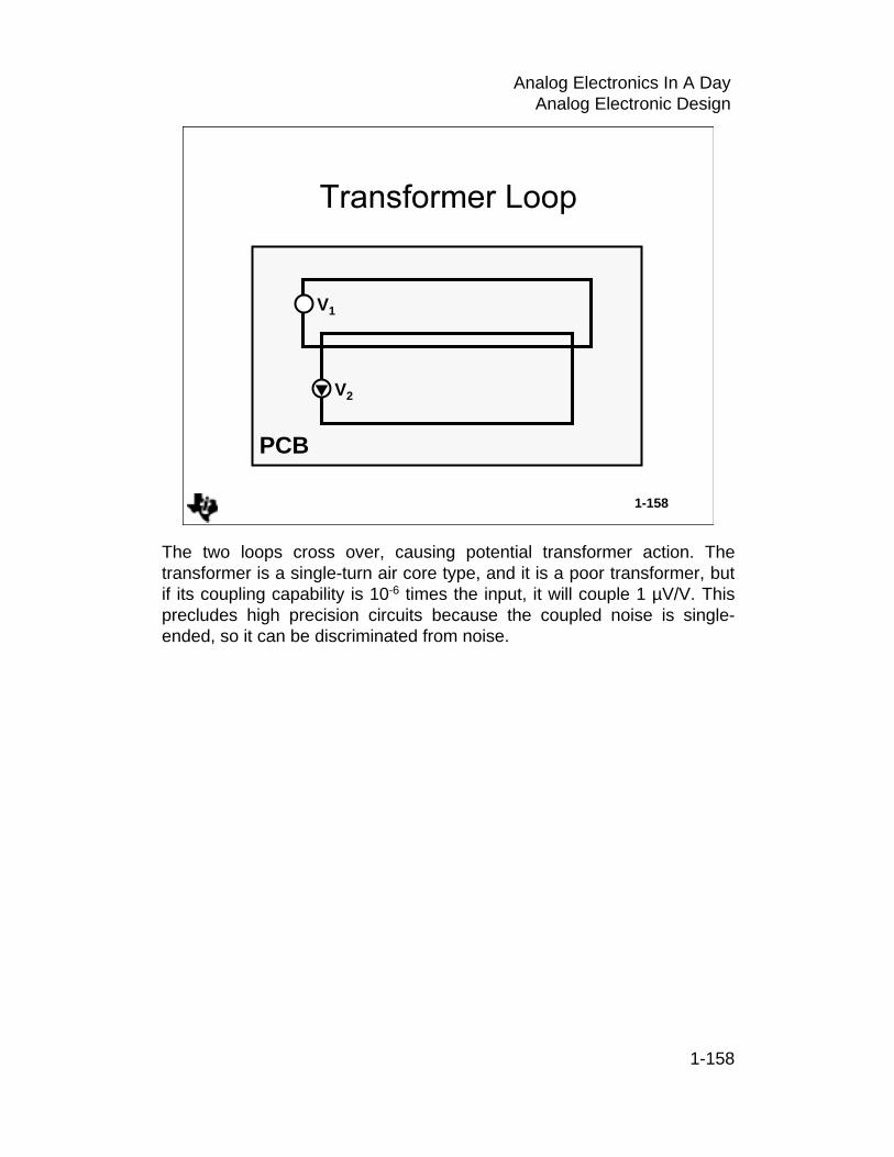
1-158
Analog Electronics In A DayAnalog Electronic Design
1-158
PCB
V1
V2
The two loops cross over, causing potential transformer action. The transformer is a single-turn air core type, and it is a poor transformer, but if its coupling capability is 10-6 times the input, it will couple 1 µV/V. This precludes high precision circuits because the coupled noise is single-ended, so it can be discriminated from noise.

1-159
Analog Electronics In A DayAnalog Electronic Design
1-159
• Use a plane if possible• A grid is next best thing to a plane• Ground return paths have inductance and
resistance• Keep return path impedance low• Keep high currents out of signal ground• Separate analog and digital grounds; tie
together at one point• Consider a star ground
The lowest power distribution impedance is a plane because of its low resistance and short path. The best recommendation is to distribute power and ground with planes. This may not be accomplishable because of cost and signal routing requirements, so when a plane can’t be used a grid is the next best choice. The grid accomplishes most the things a plane does, but it also allows traces to be run between the grid lines. Both methods keep the return impedance low.
Narrow traces and small wire do not make suitable ground returnsbecause their inductance is too high. The inductance causes peaking when transient currents flow in the return paths, and the peaking makes the noise situation worse. Separating analog and digital ground keeps the digital noise out of the analog ground system. The two grounds should be kept separate as much as possible, but some A/D and D/A converters require that analog and digital ground be connected together at the IC pins. In any case, the analog and digital ground must be connected together at the power supply. A star ground has one central point with legs going out to each circuit in a star like manner. Star grounds are usually employed on systems, but occasionally they are very effective on large PC boards that don’t have ground planes.

1-160
Analog Electronics In A DayAnalog Electronic Design
1-160
• Open wire has approximately 1nH per foot
• PC traces have approximately 10nH per inch
• Cables are inductive
• Wire bonds are inductive
• Inductance causes peaking
Inductors are all over the place, and they cause peaking which emphasizes ground spikes generated by logic and fast switching circuits. Open wire has from 1 to 10nH per foot. PC board traces have approximately 10nH per inch. A short trace or piece of wire can get to 10 nH fast, and 10 nH has an impedance of approximately 6.3Ω at 100 MHz. A current spike from a logic gate can be 50mA, so the noise generated across the inductor is 315mV.
Cables are made from wire, thus they are inductive. This means that cables are capacitive and inductive, hence cables have their own LRC circuit, and they can resonate. Wire bonds, connector pins, and, PC board connectors are inductive. Sometimes it is advisable to parallel pins to get the inductance down.

1-161
Analog Electronics In A DayAnalog Electronic Design
1-161
• Resistors have parallel capacitance and series inductance
• Power resistors will couple heat to circuits• High value resistors are less stable• High value resistors change value when
voltage is applied• Wirewound resistors are highly inductive• All resistors have noise
Resistors have parasitic components. The worst offender is a parallel capacitor which kills the bandwidth in VFAs or causes oscillation in CFAs. Power resistors are made so that they can dissipate large wattage, but the resultant heat couples to adjacent circuits causing thermal drift. High value resistors have a tendency to change resistance while under the stress of applied voltage thus leading to non-linear operation. High value resistors are drift prone, so it might be wiser to use two smaller value resistors rather than a high value one.
Wirewound resistors are highly inductive, so they should be avoided in high frequency circuits. Many potentiometers are wirewound, and these parts are not suitable for high frequency work. Use a cermet potentiometer when high frequency potentiometer is required. All resistors have Johnson noise. High value resistors are worse, and carbon film resistors are one of the least offensive.

1-162
Analog Electronics In A DayAnalog Electronic Design
1-162
The Printed Wiring Board is the pattern of interconnect - typically multiple layers of interconnect
By deciding the properties that are important it is easier to make informed decisions regarding the materials used
An increasingly important component which the designer often overlooks is the Printed Wiring Board - PWB. The decisions regarding materials used to make the PWB is typically made by the PWB manufacturer, but an understanding of the material most suited for the intended application and its advantages and disadvantages help to ensure the product performs as intended.
The most popular laminates are:-
FR-4 & FR-5 (FR - Flame Retardant),
Multiple plies of epoxy-resin impregnated woven glass cloth
CEM-1, CEM-3
Composite having dissimilar core material, e.g.paper core impregnated with epoxy resin.
GI
Polyimide resin woven glass cloth

1-163
Analog Electronics In A DayAnalog Electronic Design
1-163
• Mechanical– Flexural Strength– Glass transition temperature– Punching properties
• Electrical– Dielectric strength– Dielectric Breakdown– Dielectric Constant - Permittivity– Characteristic impedance– Propagation delay
• Flammability– UL evaluation system
The properties to consider in choosing the PWB material include
Mechanical
Glass Transition is a measure of how well a laminate resin system resists softening from heat.
Electrical
Dielectric constant is a measure of the ability of an insulating material to store electrostatic charge - important at higher frequencies.
Characteristic impedance is the impedance that a fast edge wouldencounter, typically in digital circuits a value of 100Ω - 120Ω for TTL.
The impedance varies with the dielectric thickness and line width.
The propagation delay varies with the dielectric thickness and track width, typically 0.15nS per inch.
Flammability
Extinguish time Combustion time Drip test
94V-0 <10s <10s <30s
94V-1 <30s <250s <60s
94V-2 <30s <250s <60s
note: 94V-2 material is allowed to drip flaming particles, burning briefly

1-164
Analog Electronics In A DayAnalog Electronic Design
1-164

1-165
Analog Electronics In A DayAnalog Electronic Design
1-165
Input Offset Errors:
VIE = VIO + VCMRR + VkSVR+ VN
IIB =(IIB++ IIB-)/2
IO =|IIB++ IIB-|
Gain Related Error:(Noninverting Amplifier)
211
FG
G1
2OUT
RRR
ZZaZ
1
aRR
1V
+=
++
+=
β
INV
RF
RS
VCC- ± 10 %
VCC+ ± 10 %
+a
-
RG
VOUT
VINIIB+
IIO VIE
IIB-
DC Input Referred Errors
The DC accuracy of an analog system is mainly limited by two parameters: the input offset errors and the gain-related error. The total input offset voltage is the sum of the input offset voltage, the input bias current, the common-mode rejection ratio and the supply voltage rejection ratio of the op amp. The total input offset voltage causes a DC output error. The loop gain is an important DC parameter because it is inversely proportional to the error. Ideally, this gain is infinite, however in reality it will be typically in the range of 100 dB at DC and rolls off at high frequencies.

1-166
Analog Electronics In A DayAnalog Electronic Design
1-166
For a 5 V ADC:10 bit: 1 LSB = 4.88 mV12 bit: 1 LSB = 1.22 mV
• Input offset voltage is amplified by op amp gain
* Typical parameters for good devices** CMOS devices except specials like chopper op amp
Technology
BiPolar @ BiFET @ CMOS** @VCC = ± 15 V VCC = ± 15 V VCC = 5 V
10 µV 0.3 mV 80 µV
25 µV 1.5 mV 200 µV
0.1 µV/°C 5 µV/°C 0.5 µV/°C
Parameter*
VIO (typ)
VIO (max)
∆VIO
∆T
IO
-
+ VO = 0 V
VCC+
VCC-VIO
Output
Input Offset Voltage (VIO)
An ideal op amp if both inputs are connected to ground would provide an output voltage of 0 V because the differential and common-mode voltage in that case is zero. However, the real op amp shows an output voltage which is not equal to zero. A small input offset voltage VIO between the differential inputs is imaginable, and this input offset voltage forces an output voltage other than zero.
The input offset voltage VIO of an operational amplifier is the voltage that must be applied between the two input terminals to get an output voltage of 0 Volt. The voltage VIO may be positive or negative, and this offset voltage is caused by the mismatch between input transistors of the op amp’s differential input stage. The voltage, VIO, is amplified with the gain of the amplifier. This is the open loop gain, unless external components configure the op amp for a smaller gain. In addition, the input offset voltage is dependent on the ambient temperature. The variation is from 0.1 µV/°C to several tenths of µV/°C.
Bipolar op amps have typically the lowest VIO and temperature drift. CMOS devices can achieve offset voltages of around 100 µV, which is better than BiFETs, but they cannot compete with the best bipolar devices. However, chopper stabilised CMOS op amps achieve a very low input offset voltage down to 1 µV (max).

1-167
Analog Electronics In A DayAnalog Electronic Design
1-167
The input bias current will be compensated, if the voltages V1 and V2 are equal.
Compensation Resistor RC
FG
FGC RR
RRR
+×=
RC
RFRG
VO(IIB) = 0
(IIB- = IIB+)RL
VCC+
V2
V1
I1 I2IIB
VCC-IIB
-
+
Compensation of the Input Bias Current
The effect of the input bias current can be compensated, if the voltage drop V2 at the inverting input and the voltage drop V1 at the noninverting input of the op amp are equal. The voltage V2 is calculated as follows:
(11-167-1
Assuming that the inverting and noninverting bias currents are equal and write equation 11-167-2:
(11-167-2
The resulting voltage V1 is under these conditions equal to the voltage V2:
(11-167-3−+ ×+×=×= IB
FG
FGIBC I
RRRR
IRV1
-IBFG
FG2 I
RRRR
V ×+×=
FG
FGC RR
RRR
+×=

1-168
Analog Electronics In A DayAnalog Electronic Design
1-168
A change of the common-mode input voltage of 1 V causes a change in the input offset voltage of 100 µV with a CMRR of 80 dB.
+
-
VCC-
CMRR(dB) = 20 × log ∆VIC
∆VIO
∆VO
VCC+
∆VICRL
1
0.5
0
-0.5
-1-6 -5 -4 -3 -2 -1 0 1 2 3 4 5VIC - Common Mode Input Voltage
TLC2262
VDD = ±5 VRS = 50 ΩTA = 25°C
VIO
-In
pu
t O
ffse
t V
olt
age
-m
V
Common-Mode Rejection Ratio
The common-mode rejection ratio of an ideal op amp is infinite. However, a real op amp produces a small output voltage if a common-mode voltage is applied to the inputs. The capability of rejecting the common-mode voltage is called the common-mode rejection ratio, and it is defined as follows:
(11-168-1
For an op amp with a common-mode rejection ratio of 80 dB, we get:
(11-168-2
This means that a change of the common-mode input voltage of 1 V causes a change in the input offset voltage of 100 µV.
Inverting op amps do not suffer from common-mode rejection ration effects when the amplifier inputs are permanently at ground for dual supply applications or half the supply voltage in single supply applications. The non-inverting amplifier configuration has a common-mode voltage equal to the input signal.
IO
IC
VV
log20CMRR∆∆×=
4
IO
IC10
VV =
∆∆

1-169
Analog Electronics In A DayAnalog Electronic Design
1-169
The supply voltage rejection ratio is the absolute value of the ratio of the change in supply voltage to the change in input offset voltage.
+
-
VCC ± 10 %
∆VO (kSVR)
VCC ± 10 %
RL
SVR
10µV/V10
1V
V
dB 100 ofK typical a withTLC4501 :Example
10
1V
V
VV
log 20 k
20100
IO
CC
SVR
20k
IO
CC
IO
CCSVR
SVR
==
=
×=
±
±
±
∆∆
∆∆
∆∆
Supply Voltage Rejection Ratio
The supply voltage rejection ratio kSVR of an op amp indicates how a change in the supply voltage influences the input offset voltage VIO. The change in the supply voltage may be caused by poor supply voltage regulation or bad supply voltage filtering. The parameter kSVR is usually given in dB and we can say:
(11-169-1
Rearranging this equation, we get:
(11-169-2
The results for a TLV2262A with a kSVR of typically 100 dB is given below:
(11-169-3
In a battery powered system with a supply voltage of VDD = 3 V, it is possible that the supply voltage may vary up to ± 10 %. This results into a supply voltage range from 2.7 V up to 3.3 V. With a supply voltage rejection ratio of 100 dB, the change in the input offset voltage is 3 µV.
IO
CCSVR V
Vlog20k
∆∆×= ±
20k
CC
IO
SVR
10
1VV =
∆∆
±
VV
10
10
1VV
20100
DD
IO µ==∆∆
±

1-170
Analog Electronics In A DayAnalog Electronic Design
1-170
++
×
++
+×+×++×
+=
G
F
VD
SVR
CCIC
G
F
FIBIOIOIN
G
FO
RR
1A
11
1kV
CMRRV
RR
1
RITVVV
RR
1 V∆∆α
Noise and input offset voltage long-term drift are neglected
+
-+-
RF
RG
VOUTVIN
Total DC Error Noninverting Amplifier
Equation 11-170-1 summarises all of the DC error sources in an op amp:
(11-170-1
++
×
++
+×+×++×
+=
G
F
VD
SVR
CCIC
G
F
FIBIOIOIN
G
FO
RR
1A
11
1kV
CMRRV
RR
1
RITVVV
RR
1 V∆∆α

1-171
Analog Electronics In A DayAnalog Electronic Design
1-171
2.5VVRR
VRR
1RR
RV 2
2
41
2
4
31
3O +×−×
+×
+=
:RR
RR
for1
3
2
4 = ( ) 2.5VVVRR
V 211
3O +−×=
Sensor
R-∆R R+∆R
R+∆R R-∆R
TLE2425
VO
2.5 V VCC+
R3
R1
R2
R4
VCC+
VCC+
-TLC4501
+
Precision Single Supply Differential Amplifier
This is the classic differential amplifier (subtractor) in a single supply environment, and it is the simplest way to measure and amplify the potential difference across a Wheatstone Bridge.This amplifier uses the non-inverting and inverting inputs of the op amp. The op amp is dc-biased with half the supply voltage at the non-inverting input to enable single supply operation which allows a maximum symmetrical voltage swing at the output. The "TLE2425 Virtual Ground Generator" is the ideal device because it generates exactly the reference voltage VREF = 2.5 V from a voltage in the range of 4 - 40 V. The voltage at the output of the op amp is calculated as follows:
(11-171-1
When the resistors are chosen as shown below: (11-171-2
an easy practical result is obtained:
(11-171-3
since for an input voltage of V1=V2, the output of the op amp delivers theoretically exactly the middle voltage VO = 2.5 V. The disadvantages of this circuit are that its input impedance is unbalanced and the common mode rejection is modified by the source impedances. This circuit is therefore not recommended for high impedance sources.
REF22
41
2
4
31
3O
RR
)RR
(1RR
RV VVV +×−×+×
+=
REF211
3O )(
RR
V VVV +−×=
1
3
2
4
RR
=RR

1-172
Analog Electronics In A DayAnalog Electronic Design
1-172
( ) 2.5VR
R21VVV
2
121O +
×+×−=
TLE2425
-TLC4501
+
-1/2
TLC4502 +
+1/2
TLC4502 -
Sensor
R-∆R R+∆R
R+∆R R-∆R
V1
VO
VCC+
VCC+
VCC+
VCC+R1
R2
R1
R3 R3
R3
R3
VCC+2.5 V
V2
Instrumentation Amplifier
A very high input impedance can be achieved by using an instrumentation amplifier. Such an amplifier consists of three op amps. The differential amplifier discussed before can be found again with a gain of 1, because all resistors are the same. Two further op amps are connected in the front of this differential amplifier to provide the very high input impedance which is determined by the op amp input impedance. The signal source connected to the instrumentation amplifier is loaded by the high input impedance of the CMOS op amp (TLC4501) which is typically 1012 Ω. The gain is adjusted by the resistor R2. The output voltage can be calculated as follows:
(11-172-1
It is very important to select the resistors with high accuracy relative to each other to achieve high common mode rejection. This can be achieved with a resistor array network where the relative accuracy is very good (value in the region of 10 kΩ). The absolute accuracy of the resistors is not as important.
REF2
112O V+)
RR2
+(1)(V××−= VV

1-173
Analog Electronics In A DayAnalog Electronic Design

1-174
Analog Electronics In A DayAnalog Electronic Design
1-174

1-175
Analog Electronics In A DayAnalog Electronic Design
1-175
• Amplifier analysis in previous section assumed no input or output voltage boundaries
• Amplifiers require two power pins:
– Dual Supply ( +5V , -5V)
– Single Supply ( +5V , Ground)
• Bias voltage (virtual ground) can be required for single supply systems
This section will focus on single supply operational amplifier applications. We will look at several simple circuits. The object is to look at some actual issue regarding circuit design and biasing.
The previous sections on amplifier analysis did not take into consideration any input or output boundaries. The following circuits will illustrate the need to consider power supply values when designing an Op Amp circuit.
First we need to make clear the definition of single supply operation. When an amplifier operates between a single voltage and ground it is called single supply operation. The same amplifier operated between positive and negative supply voltages is called dual supply operation.
When an amplifier is used in the single supply mode a bias or reference voltage is often required. This bias voltage is also called a virtual ground.

1-176
Analog Electronics In A DayAnalog Electronic Design
1-176
1k10k10
VV
RR
VV
IN
OUT
G
F
IN
OUT
−=ΩΩ=
−=
Operating conditions:VIN= 4 V peak-to-peak
(+2V to -2V)Power supply +5V, -5V
Inverting amplifier gain equation:
RG10 kΩ
RF10 kΩ
RL10 kΩ
TLC2272+
–+
+
–
5 V
5 V
VIN
VOUT
VB
The circuit above is operated in a dual voltage mode (+5V and -5V) with proper biasing (Both VIN and VOUT referenced to ground).
Using the differential amplifier formula:
For this circuit we do not have the divider network R2 ,R1 and VB=0 so the first term becomes 0 and the formula becomes:
Now consider the operating conditions. The output voltage must be within the limits of +5V and -5V. For this circuit VIN is 4V peak to peak (+2V to -2V).
G
FIN
G
GFBOUT R
RV
RRR
RRR
VV −
+
+=
122
INOUT
ING
FINOUT
VV
kk
VRR
VV
−=ΩΩ−=−=
1010
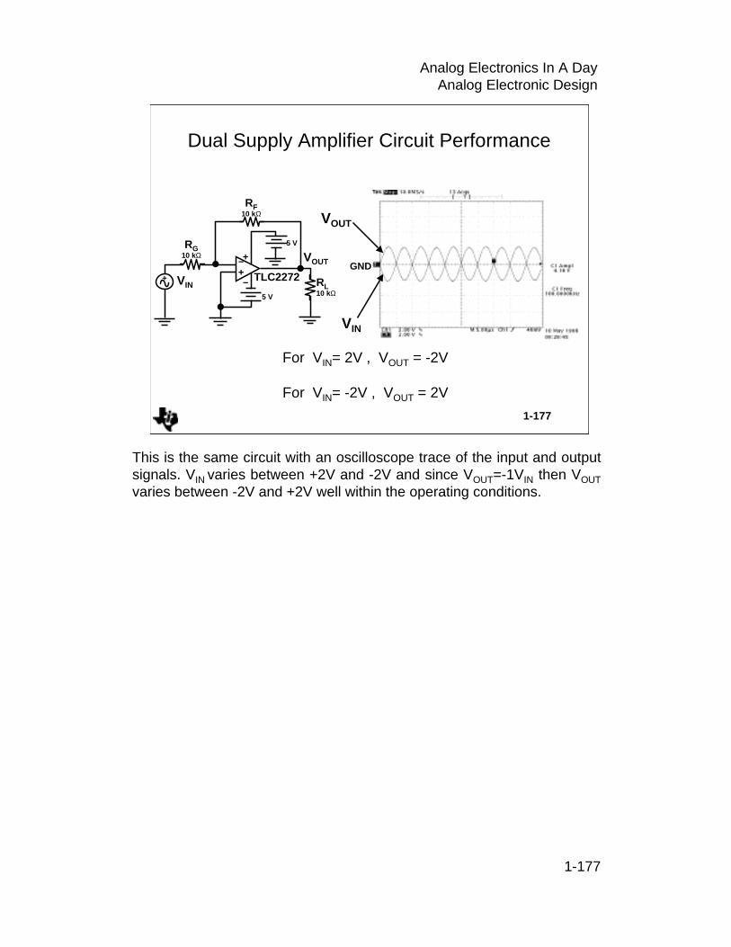
1-177
Analog Electronics In A DayAnalog Electronic Design
1-177
Dual Supply Amplifier Circuit Performance
GND
VIN
VOUT
For VIN= 2V , VOUT = -2V
For VIN= -2V , VOUT = 2V
RG10 kΩ
RF10 kΩ
RL10 kΩ
TLC2272+
–+
+
–
5 V
5 V
VIN
VOUT
This is the same circuit with an oscilloscope trace of the input and output signals. VIN varies between +2V and -2V and since VOUT=-1VIN then VOUT varies between -2V and +2V well within the operating conditions.

1-178
Analog Electronics In A DayAnalog Electronic Design
1-178
• Same Amplifier circuit powered by +10V and Ground.• The input waveform, VIN and RL referenced to GND• VIN = 4.0Vp-p @ 100kHz• VOUT is a half-wave signal
VIN = -2V , VOUT = 2VVIN = 2V , VOUT = Ground
GND
VIN
VOUT
10VRG10 kΩ
RF10 kΩ
Rl10 kΩ
TLC2272+
–+
+
–VIN
+VDD
VOUT
VB
Now consider the same amplifier modified to operate in the single supply mode. The supply voltages are now +10V and ground. And the non-inverting amplifier input VB is still at 0V. The total voltage across the amplifier is still 10V. However now the output is restricted to +10V and ground (0V). This circuit has the same input signal as the previous example (+2V and -2V) and the same gain (-1). This circuit cannot work properly since the output voltage is now restricted to +10 and 0V. The result is an output (VOUT) that can only from 0V to +2V. The negative portion of the output is clipped at 0V.
This circuit is incorrectly biased.

1-179
Analog Electronics In A DayAnalog Electronic Design
1-179
INOUT
INOUT
G
FIN
G
GFBOUT
V10VV
(1)V1)5V(1V
RR
VR
RRVV
−=−+=
−
+=
VB = 5V
GND
IN
OUT
VIN VOUT
0V 10V+2V 8V-2V 10V
5V
10VRG10 kΩ
RF10 kΩ
Rl10 kΩ
TLC2272+
–+
+
–VIN
+VDD
Vb
This is the same circuit again with a change on the bias voltage VB. This circuit has VB=5V. The formula for a differential amplifier is:
Remember from the previous example the R1, R2 divider equals 1. Unlike the previous example VB is now 5V.
Therefore:
Now look at the operation with a +2V and -2V input signal. Again we have an incorrectly biased circuit.
G
FIN
G
GFBOUT R
RV
RRR
RRR
VV −
+
+=
122
( )
( )
INOUT
INBOUT
INBOUT
G
FIN
G
GFBOUT
VV10V
VV2V
k10k10
Vk10
k10k101VV
RR
VR
RR1VV
−=
−=
ΩΩ−
ΩΩ+Ω=
−
+=

1-180
Analog Electronics In A DayAnalog Electronic Design
1-180
GND
• Bias voltage is applied to VIN, RL, & non-Inverting input.• Input and output waveforms swing freely about VB
IN
OUT
SIGBBSIGBOUT
INBG
FIN
G
GFBOUT
BSIGIN
VV)(1)V(V2VV
10k10k
V10k20k
VRR
VR
RRVV
VVV
−=+−=
−
=
−
+=
+=
5V
–+
Ri10 kΩ
Rf10 kΩ
+ VIN Rl10 kΩ
+
–
10V
TLC2272
Vb
VB
This example shows the correct way to bias an inverting amplifier circuit. VB is applied to both the amplifier non inverting input and to the input signal.
Examination of the output signal show the following:
VSIG VOUT
-2V 7V
0V 5V
+2V 3V
The output is a 4V peak-to-peak signal centered around VB (5V)
SIGBBSIGBOUT
INBG
FIN
G
GFBOUT
BSIGIN
VV)1)(VV(V2V
k10k10
Vk10k20
VRR
VR
RRVV
VVV
−=+−=
ΩΩ−
ΩΩ=
−
+=
+=

1-181
Analog Electronics In A DayAnalog Electronic Design
1-181
• Capacitor (Ci) blocks the flow of dc current• Output is an inverted version of the input referenced to VB
•
• Capacitor makes the system frequency dependent• Low frequency cutoff point; f = 1/2∏CiRi (f = 159Hz)
+−
++
=i
fi
i
fBO
RsCi1
RV1
RsCi1
RVV
GND
IN
OUT
–+
+
+
–
Ri10 kΩ
Rl10 kΩ
TLC2272VIN
10V
Vb5 V
Ci0.1 µF
Rf10 kΩ
The previous examples were for DC coupled circuits. A DC coupled circuit amplifies both the AC and DC components of the input signal. The circuit above is an AC coupled circuit. C1 isolates the input signal and allows the circuit to be properly biased while having the input signal referenced to ground instead of VB as in the DC coupled circuit.
The disadvantage of AC coupling is the zero in the gain equation causing this to be a low pass filter with a breakpoint of 159Hz.

1-182
Analog Electronics In A DayAnalog Electronic Design
1-182
Example 1
Rl
IL
Advantages:Simple circuitNo bias required on load
Disadvantage:When VIN=0 VOUT=5V and IL = 5/RL
5V
–+
Ri10 kΩ
Rf10 kΩ
+ VIN Rl
+
–
10V
TLC2272
Vb ?
Example 2Advantages:
When VIN=0 IL=0Disadvantage:
IL flows through VBcausing errors due tointernal resistance of VB
RL
VB Ri
IL
The last topic for this section is load considerations. First you must consider that any current flowing through the load must come from the power supplies. Next as in the previous cases you must consider bias voltages on the load resistor.
Example 1 shows Rl referenced to ground. In this example with a single supply amplifier, VOUT equals VB when VIN is 0V. The result is current flowing in the load resistor when no input signal is present.
Example 2 shows RL biased to VB. Now VOUT equals VB when VIN is 0V and the voltage across RL is 0V. The result is no current flows when no input voltage is applied. The disadvantage is that the load current flows through VB. The example show the actual model for a battery or power supply. Notice that the model includes an internal resistance. Remember from the analysis earlier current flowing through the internal resistance will result in a voltage drop and can possibly cause errors if other portions of the circuit use the same bias voltage VB..

1-183
Analog Electronics In A DayAnalog Electronic Design
1-183
• Simulation programs are a tool.• They will not design a circuit.• They are not a substitute for common
sense• Use
– Can predict failure– Not a reliable predictor of success
• Lab testing is required
Analog circuit simulation programs are a tool that can aid in evaluating a circuit design. When used wisely these tools can help in the design process. Just remember that the program will not design a circuit for you.
These programs perform a mathematical analysis of the circuit based on models and the information you supply. The accuracy of any such calculations depends on the models used , the accuracy and the amount of information supplied. Simple descriptions which ignore many of the frequency related factors and intrinsic errors yield simplistic answers.
Also just remember if you cannot get the circuit to work on the simulation it probably won’t work on the actual circuit, however if it works on the simulator it may or may not work on the actual circuit.

1-184
Analog Electronics In A DayAnalog Electronic Design
1-184
• Biasing is important especially in single supply amplifier circuits.
• Always consider the power supply limitations when evaluating circuit performance
• Both Ohm and Murphy can give you problems if you aren’t careful.

1-185
Analog Electronics In A DayAnalog Electronic Design

1-186
Analog Electronics In A DayAnalog Electronic Design
1-186

1-187
Analog Electronics In A DayAnalog Electronic Design
1-187
• Voltage Feedback and Current Feedback Amplifier Performance.
• Where Are They Used?
• High Speed Data Converter System.

1-188
Analog Electronics In A DayAnalog Electronic Design
1-188
• High impedance differential input stage (i.e. no current flow at input)
• Bandwidth a function of closed loop gain - GBWP
• Internal slew rate limitations
• VF amps are the easiest to use
• Traditional design techniques
+
+
-
VdAOL
Vo
0.001 0.01 0.1 1 10 100
Frequency - MHz
80
60
40
20
0
-20
Ou
tpu
t A
mp
litu
de
-d
B
Vd
First, let’s talk about the classic voltage feedback amplifier. The voltage feedback amplifier (VFB) has a high impedance input stage. The amplifier first looks at the difference in voltage (Vd) at the inverting and non-inverting terminals. The output then multiplies the difference (Vc) by the open loop gain (AOL). With negative feedback from the output to the inverting node, we get a closed loop amplifier.
One of the main characteristics of a VFB amplifier is the bandwidth is indirectly related to the gain. As the gain is increased, the bandwidth is divided by the gain. This is known as Gain Bandwidth Product - or GBWP.
For example, if we look at the graph on the lower right corner, it shows a -3dB bandwidth of about 100 MHz at a gain of one. If we set the gain to 40 dB , or 100, then the bandwidth is divided by 100, or 100Mhz / 100 = 1 MHz.
As stated previously, the VFB amplifier does have internal slew rate limitations based on it’s architecture. Because of this, VFB amps are generally used in lower bandwidth systems. And because it has high input impedances, the VFB amplifier is extremely easy to use. Making an integrator or a simple buffer is no problem with a VFB op-amp. This is because the op-amp does not rely on the current flowing into or out of the input stage.

1-189
Analog Electronics In A DayAnalog Electronic Design
1-189
• Much higher slew rates
• Unity Gain Buffer Input Stage
• + input has high impedance
• - has low impedance (i.e. current flow)
• Internal transimpedance stage
• Much higher slew rates
• Bandwidth ‘independent’ of gain
• Harder to use
• Must have feedback resistor
• NO capacitor in feedback path
+
-Ierror
+ZIerror
Vo
x1
80
60
40
20
0
-20
0.01 0.1 1 10 100 1000
Frequency - MHzO
utp
ut
Am
plit
ud
e -
dB
The first thing you will notice is that the input stage is quite different. The non-inverting input has a high input impedance, just like the VFB amplifier. But, the inverting stage is low impedance, typically less than 20 ohms. This means that current will flow into this pin. The output will then multiply the error current (Ierror) by the open loop transimpedance (Z). With a feedback resistor placed between the output and the inverting pin, we form a closed loop system.
The first thing you will notice is that the feedback resistor limits the amount of current flow into or out of the inverting pin. And because bandwidth is determined by the amount of current available to charge the internal compensation capacitor, the feedback resistance plays the key role in determining the bandwidth of the system. Typically, as the feedback resistor is increased, the bandwidth will be decreased.
Additionally, the slew rate will also be affected by this same concept. To find out exactly what the feedback current will be, we get the following equation :
IFEEDBACK = ( VOUT - VINVERTING NODE ) / RFEEDBACK
Remember that the slew rate is determined by the current available to charge the internal dominant pole capacitor. Thus, the slew rate is determined by the output swing and the feedback current into theinverting node.

1-190
Analog Electronics In A DayAnalog Electronic Design
The last key feature of this system can be seen in the frequency response graph of a typical current feedback amplifier. There is not a gain bandwidth product like there is in a VFB amplifier. Thus, once you get an acceptable response out of a CFB amplifier, you simple need to change the gain resistor to change the overall system amplification, not the feedback resistor. Again, the feedback resistor controls the response of the CFB amplifier.
As stated before, the drawback to the CFB amplifier is the fact that it can be harder to use. But, careful planning will make this amplifier as easy to use as the VFB amplifier. So, if you need an extremely high slew rate, gain independent, high bandwidth amplifier, the CFB amplifier makes a logical choice.

1-191
Analog Electronics In A DayAnalog Electronic Design
1-191
TYPE VF.B CF.B
PN THS4.001 THS3.001
Bandwidth (MHz) 300 420
Slew Rate (V/µs) 400 6500
Settling time (ns) 30 40
IO (mA) 100 100
THD (dBc@1MHz) -72 -96
Diff Gain Error (%) 0.04 0.01
Diff Phase Error (%) 0.15 0.02
The chart shows performance of two actual high speed amplifiers. The difference in performance between a current feedback and voltagefeedback amplifiers can be seen especially in the bandwidth and slew rate specifications. Some of these specifications have not previously been mentioned. Slew rate is the rate at which the output can change when a square wave is applied to the input. Both differential gain and differential phase errors are terms associated with video and describe the amplifiers performance with signals of different amplitudes.

1-192
Analog Electronics In A DayAnalog Electronic Design
1-192
Mem
ory
ADCATT
ATT ADC
VideoDACs
DSP
High Speed OPAMP
Channel 1
Channel 2
X Amp
X Amp
CRT
High speed op amps are used in numerous applications. The example above is a digital oscilloscope. High speed op amps are used input signal conditioning on each channel prior to being fed into ADCs. Some of the things which would be important in this application are; high bandwidth, high input impedance, high output drive and a circuit design which would have accurate gain and closely match the performance of both channels.

1-193
Analog Electronics In A DayAnalog Electronic Design
1-193
CRT
Mem
ory
High ResolutionCamera ADC Video
DACs
DSP
High Speed OPAMP
X Amp
X Amp
FluoroscopeImage
Intensifier
X-Ray Source
Another application using video is a Digital X-Ray System. This is real time system so the data from the camera occurs at a video rate. The important things are similar to the previous circuit: high bandwidth, high input impedance, high output drive. These circuits would require low differential and phase errors since imaging/video is involved.

1-194
Analog Electronics In A DayAnalog Electronic Design
1-194
DSP
LPF
DAC
HPF PGA
DSP
Transceiver(HS Amps)
LPF
ADC
DAC
Copper Pair
This circuit is a high speed ADSL modem. The ADSL modem operatesover conventional copper telephone wiring using special equipment at both the telephone company central office and at the user’s residence. The system sends digital data over the line containing both voice and data information. Data rates are much higher than those accomplished with conventional modems.
This system would use high speed amplifiers in the high pass filter (HPF), low pass filters (LPF), and programmable gain amplifier. The block labeled transceiver is also a set of specialized high speed amplifiers.

1-195
Analog Electronics In A DayAnalog Electronic Design
1-195
• 8 Bit Resolution • 40 MHz Sampling
R8820 Ω
U2THS30013 76
2 4
5 VA
C84.7 µF
C70.1 µF
+
R449.9 Ω
–
+C194.7 µF
C160.1 µF
ANALOG IN
VDDA
ADC
TLC5540
C14*
+–
-5 VA
5 VA
C64.7 µF
+
R549.9 Ω
19
R210 kΩ
R121 kΩ
R111 kΩ
5 VA
R6820 Ω
Analog Input
100pF
Here you can see the front-end of an analog - to - digital converter (ADC). This particular converter requires a single supply and thus the input signal must also be uni-polar. To create this, the amplifier is DC shifted to the mid-rail, creating a virtual ground to the ADC input. A signal is then AC coupled into the amplifier. The DC bias and AC input signal are amplified by two. To help eliminate any glitches, a simple low pass filter is placed between the amplifier and the ADC. This also helps in isolating the capacitive load. The 49.9 ohm resistor (R4) is used for stability.
Notice that even though the amplifier is high speed the circuit topology is similar to many other circuits. The difference would be in the actual printed circuit design which wold require special layout considerations.

1-196
Analog Electronics In A DayAnalog Electronic Design
1-196
• High speed amplifiers are used in numerous applications.
• Although the circuit diagrams are similar the physical circuit layout is very critical when using HS amplifiers.

1-197
Analog Electronics In A DayAnalog Electronic Design

1-198
Analog Electronics In A DayAnalog Electronic Design
1-198

1-199
Analog Electronics In A DayAnalog Electronic Design
1-199
Time Time
Continuous values Discrete integer values(quantized)
Bridge
Data Converter
What is a Data Converter
Data converters serve as the bridge between the analog and digital worlds. Data converters provide the electrical conversion between analog signals and digital signals.
What is analog, what is digital? Maybe this is a little fundamental, but it is kind of a mind set. Analog signals are continuous. Analog things are continuous, something that happens over a continuous function. There are no discontinuities in it. Digital is discreet, quantized things. We deal with both of those every day. We merely quantize things. You don’t realize it, but you are quantizing things. An example is, how many of you stepped on the scale in your bathroom this morning? No? As you get older, you’ll do that. You step on the scale, it has a dial on it, not digital numbers. Mine says, looks like about 190 pounds. It was 196, but I said 190. I quantize that to a nice even value that I am comfortable with. If I quantize it to 200, I have to go on a diet, so I use a 4 bit quantization to make sure I’m happy with quantizing. We do it all the time.

1-200
Analog Electronics In A DayAnalog Electronic Design
1-200
• A Digital number is loaded into converter.
• Logic circuitry controls switches.• Switches select from one or more
analog reference voltages or currents.• Resulting analog signal is output.
The basic operation of a DAC is similar to that of the ADC. A digital number, representing an analog sample is loaded into the DAC input. The digital number is input to logic circuitry which controls a set of analog switches. The analog switches now select from a set of referencevoltages or currents. The results of the selection represent the number with an analog output. The analog signal is now buffered and in some ADCs applied to a sample and hold.
The use of a sample and hold prevents transients in the analog output due to the switches changing state as a result of loading a new number into the input. The input digital number is normally loaded into a register.

1-201
Analog Electronics In A DayAnalog Electronic Design
1-201
SW
ITC
HE
S
2N -1
Res
isto
rs
VREF
INPUT CODE
VOUT
In a Resistor String architecture, the reference voltage is divided into 2N -1 parts, each exactly one LSB high. A network of switches selects the output voltage from the resistor string, depending on the digital input code. To avoid errors due to a load current, a buffer is required on the DAC output. This buffer is usually part of the DAC. The big advantages of this architecture are, that the transfer function is always monotonic and that the design is relatively simple. The disadvantages are, that 2N - 1 matching resistors are required, which limit the achievable resolution and that this architecture needs an amplifier (buffer), which limits the achievable speed.
Other architectures use different methods such as selecting a binary weighted divider which effectively sums currents to achieve the selected values for the final result.

1-202
Analog Electronics In A DayAnalog Electronic Design
1-202
Digital Change Delay Time t
Slew Rate
Glitch
Settling Time, ts
Final Value
ErrorBand
An
alo
g O
utp
ut
(V)
Settling Time of a D/A Converter
The settling time of a D/A-converter is the time between the switching of the digital inputs of the converter and the time when the output reaches its final value and remains within a specified error band. The settling time is a very important parameter, because this must be faster than the signal frequency in order to be able to reconstruct the waveform. The picture shows also a possible glitch in the waveform of a DAC. This glitch is an undesirable transient in the analog output occurring following a code change at the digital input. If a current output DAC is used with an external amplifier, then a ferrite bead can be used to minimize the glitch by minimizing the switching current.

1-203
Analog Electronics In A DayAnalog Electronic Design
1-203
• Resolution (Bits)• Settling time• Reference• Errors/Distortion• Clocks• Coding
The important considerations for a DAC are resolution, settling time, reference and errors. Resolution for a DAC like that of the ADC determines the maximum SNR achievable. Settling time is the equivalent of conversion rate. Settling time determines which analog signalfrequencies can be reproduced. The reference voltage impacts accuracy and stability. Errors/distortion determine how accurately waveforms can be reproduced and are covered in the next pages.

1-204
Analog Electronics In A DayAnalog Electronic Design
1-204
• Analog signal is sampled• The sampled analog signal is compared
to one or more reference voltages• The result of the comparison is
converted by digital logic to a binary number.
Basic ADC Theory
The basic ADC converts an analog signal digital by first sampling the signal. Second the sample is compared to a set of reference voltages. The result of the comparison is then converted by logic circuitry to a binary number. The binary number is the converter output.
Several different system architectures are used to implement ADCs. They differ in how the signal is compared to the reference and how the output is configured.

1-205
Analog Electronics In A DayAnalog Electronic Design
1-205
Input SpectrumF(f)
f1 f
Sampled SpectrumG(f)
f1 ffs fs+f1 2fs-f1
Sampled Output
t
g(t)
t1 t2 t3 t4
f(t4)f(t3)f(t2)
f(t1)X =
=
Sampling Function
Unit Pulsesh(t)
tT
Fourier Transform
NYQUIST’S THEOREM: fs-f1 > f1 fs > 2 × f1
Input Waveformf(t)
tt1 t2 t3 t4
Sampling SpectrumH(f)
ffs = 1/T 2fs
Nyquist region
Sampling Theory Overview
In order to produce a discrete digital representation of a continuously varying analog signal, it is necessary to take samples of the signal at regular intervals and convert them from analog into digital. In an ideal situation the sampling function is a train of impulses, each of which is infinitesimally narrow and has unit area. The frequency of these pulses is the sampling rate (fs). The input signal can also be idealized by considering it to be truly band limited, containing no components in its spectrum above a certain frequency.
The ideal sampling condition, represented in both the frequency and time domains, is shown in the figure above. The effect of sampling in the time domain is to produce amplitude modulated train of impulses representing the value of the input signal at the instant of sampling. In the frequency domain the spectrum of the pulse train is a series of discrete frequencies at multiples of the sampling rate. Sampling convolves the spectrum of the input signal with that of the pulse train to produce the combined spectrum shown, with sidebands around each discrete frequency produced by the amplitude modulation. In effect some of the higher frequencies are “folded back” so that they produce interference at lower ones. This interference causes distortion, which is called aliasing. Aliases cannot be removed by subsequent processing.

1-206
Analog Electronics In A DayAnalog Electronic Design
1-206
RS
VINVSample
CHOLD
ADC
Sample & Hold Conversion
Sample and Hold
The basic sample and hold circuit is a switch and a capacitor. To sample the signal the switch is closed, applying VIN to CHOLD. The switch is opened and the value of VIN is “held” by the charge on CHOLD while the ADC performs the analog to digital conversion.
The purpose of the sample and hold is to take a “sample” of the analog input signal and “hold” the value while a conversion takes place. This is particularly important for ADCs which take a number of steps to make the conversion. Without the sample and hold errors can occur in the conversion.

1-207
Analog Electronics In A DayAnalog Electronic Design
If we assume that the input signal is band limited to a frequency f1 and is sampled at frequency fs it is clear from the figure that the overlap (and hence aliasing) will not occur if
f1 < fs - f1This could also be expressed by: 2f1 < fs
Therefore, if sampling is done at a frequency at least twice as great as the maximum frequency of the input signal, no aliasing will occur and all the signal information can be extracted. This is Nyquist’s Sampling Theorem, which provides a basic criterion for the selection of the sampling rate required by the converter to process an input signal of a given bandwidth.
In real sampling, however, the width of each sample is finite and this gives rise to a modulation error of (sin x) / x. This is explained later.
Real world signals are generally not band limited. To avoid errors due toaliasing an anti-aliasing filter is normally used. This filter band limits the signal and minimizes any errors due to aliasing. Anti-aliasing filters can be either external or internal to the data converter.
When designing a system it is necessary to know the input signalcharacteristics in order to select a sampling rate and filters, if necessary, for minimum conversion errors.

1-208
Analog Electronics In A DayAnalog Electronic Design
1-208
Reference
VIN
fS
+-
S/H
VREF
DOUT
Comparator
VCC
GNDVCC = 1GND = 0
Least significant Bit (LSB) the smallest measurable value.LSB = VREF
For: VIN < VREFVOUT = GND
VIN > VREFVOUT = VCC
The simplest data converter is a single comparator. The unknown analog voltage VIN is applied to the non-inverting (+) input of a comparator. A reference voltage is applied to the inverting (-) input. If VIN is greater than VREF then the output will go to VCC (Digital 1). If VIN is less than VREF then the output will go to ground (Digital 0).
The least significant bit repersents the smallest analog voltage that can be measured. In this example this would be VREF.

1-209
Analog Electronics In A DayAnalog Electronic Design
1-209
N = Resolution of ADC1 LSB =VFULLSCALE(nom.)
2N
N = 8 10 12 14 16 20
1 LSB 39.06 9.77 2.44 610 153 9.53± 5 V input range mV mV mV µV µV µV
1 LSB 19.53 4.88 1.22 305 76.3 4.77 + 5 V input range mV mV mV µV µV µV
1 LSB 11.72 2.93 732 183 45.8 2.86+ 3 V input range mV mV µV µV µV µV
2-16
How Large is a LSB ?
A code of an ADC represents a specific voltage magnitude, which is given by
Where N is the resolution of the ADC. The figure shows the magnitude of a LSB for different resolutions and different analog input voltage ranges. It‘s obvious that the LSB is getting very small if the ADC provides a high resolution or the analog input voltage range is small. The figure shows LSB values smaller than 1 mV. Therefore, it is a challenge to keep the error (offset, drift, noise), which is caused by the signal conditioning stage below an LSB of the ADC.
VFS (Practical Full-Scale Range) is the total range of analog values that correspond to the ideal transfer line.
N
)nom(FS
2V
LSB1 =

1-210
Analog Electronics In A DayAnalog Electronic Design
1-210
Ref
VIN
MSB
LSB Dat
a O
ut
fS
+-
S/H
Clock SAR and Control Logic
D/A Converter
Disadvantages:•Requires N sequential comparisons•Low to moderate speed
MSB LSB
FS
FS: Full Scale
0
FS2
Advantages:•General purpose •Cost effective
Successive Approximation ADC
Successive approximation is a common technology for A/D converters. A conversion time from 100 µs to below 1 µs and a resolution up to around 16 bits is possible and make this type of ADC still the most popular type of converter.
Successive comparison of an unknown analog input voltage with binary weighted values of a reference give this method its name of “successive approximation”. A converter of N-bit resolution takes “N” steps to achieve a digital output.
VIN is applied via a sample and hold to one input of a comparator, while the output of a DAC drives the other input. The successive-approximation register (SAR) provides the input to the DAC. When the DAC has its MSB set to logic level 1 (with all other bits zero) by the successive-approximation register (SAR), it will produce a voltage output of 1/2 the reference (analog input full-scale range). The comparator then determines if the DAC output is above or below the unknown input signal. If, as shown, the input signal VIN is above the DAC output value, the MSB is retained in the successive-approximation register while the next weight of 1/4 the reference is compared. This process continues until all bits are tested and the nearest approximation to the input signal is obtained.

1-211
Analog Electronics In A DayAnalog Electronic Design
1-211
Disadvantages: High power
High cost
Size of Circuit
n . . . 1 0 1 0 0. . . 1 1 0 0 1
Analog Input
Clock
R/2
R/2
2n - 1 Comparators
R
R
VREF
Dec
od
er
Lat
ch
+-
+-
+-
Advantages: High Speed
Flash Converter (2 Bit)
The flash analog to digital converter provides the fastest conversion method today. This is achieved by a simultaneous comparison of the analog input signal with 2n–1 reference voltages. These reference voltages are generated with a voltage divider, which is built by a resistor chain. Each reference voltage is connected to the inverting input of a comparator. Again, for an n-bit resolution, 2n–1 comparators are required with threshold voltages varying by 1 LSB. The analog input signal is connected to the noninverting input of every comparator. The output is low for every comparator where the analog input signal is smaller than the reference voltage. The output is high for every comparator where the analog input signal is higher than the reference voltage. The decoded digital output data, which is n bits wide, is written into a latch.
As previously mentioned, flash converters have been favored for achieving high sample rates. However, the flash method requires 2n-1comparators to implement an n-bit converter. This means that 255comparators are needed for an 8-bit ADC and 4095 comparators for a 12 bit flash converter. Flash converters therefore occupy a relatively large area of silicon, require a lot of power, have a high input capacitance and are expensive.

1-212
Analog Electronics In A DayAnalog Electronic Design
1-212
PARALLELDIGITALOUTPUT
ANALOGINPUT
+-
STAGE N
+-
STAGE 1
Sample HoldAmplifier
SAMPLE HOLDAMPLIFIER
Sample HoldAmplifier
Σ Σ
DAC
REGISTER
DACADC
REGISTER
ADC
ADC
Flash
Advantages:• High speed• Cost & power effective
Disadvantage:• Pipeline delay (Latency)
N Stage Pipelined ADC Architecture
Higher sample rates than successive approximation techniques can be achieved cost effectively by using the pipelined architecture. The functional block diagram of this conversion method is shown in the picture. It consists of a number of individual n-bit resolution (typically n = 2 or 4) converter stages which are cascaded to form the complete converter. Each stage comprises of an n-bit ADC, an n-bit DAC, a sample/hold amplifier and a data register. The sample/hold should be N bits accurate where N is the resolution of the overall ADC.
The ADC operates as follows. The analog input signal is sampled and held. The first stage produces the first n MSBs of the overall ADC conversion result. This n-bit result is then reconverted back into analog form via the n-bit DAC and is subtracted from the held input signal level. The result of this subtraction is then sampled and held. The next stage then repeats the process performed by the previous stage and this in turn is repeated for subsequent stages. The instant that the result of the subtraction of stage 1 is successfully held, the preceding sample/hold amplifier acquires the next sample of the input signal. This allows the individual n-bit conversions to occur serially in time. Thus the throughput rate of the overall ADC is increased significantly. In addition, the chip area is significantly reduced from that which would be needed with a full Flash architecture.

1-213
Analog Electronics In A DayAnalog Electronic Design
1-213
Σ ∆
AnalogInput
1-bitwide
n-bitswide Digital
OutputDigitalFilter
AnalogModulator
Sample/HoldAmplifier
Advantages:• Minimum analog components• Integrates easily with digital logic• Oversampling reduces inband
noise
Disadvantages:• Speed limited to upper audio
range
Sigma-Delta Converters – Functional Block Diagram
The simplified structure of a Sigma-Delta ADC is shown in the figure above and comprises an analog modulator and a digital filter. The analog modulator, running at a high sampling rate, converts the input signal at its output to a 1-bit pulse density modulated bit stream. The digital filter takesthis bit stream and simultaneously removes out of band noise andreduces the bit rate while increasing the output word width.
To increase resolution the analog modulator not only oversamples the input signal but also shapes the quantization noise so it appears in the unwanted band to be removed by the digital filter.
The one bit quantization in the analog modulator provides low differential non-linearity and hence no missing codes in the output. The high input sampling rate means only a non-critical anti-aliasing filter is required and a sample and hold is not required.
The resolution of a Sigma-Delta converter is determined from its output signal to noise ratio.

1-214
Analog Electronics In A DayAnalog Electronic Design
1-214
Σ ∆D
+Vref
Vin = Vref/2
-Vref
t
A1.5 Vref
t-0.5 Vref
B0 V
C
0 1 1 1 01 1 1 0 1 11 0 11 14 Bits
+-
D
C
BVin
+Vref
-Vref
DifferentialAmplifier Integrator Comparator
DigitalOutput
DAC
A +-
1st Order Modulator
The analog modulator performs the actual analog to digital conversion process. In its simplest form this consists of a differential amplifier, single integrator, comparator and 1-bit DAC connected in a closed loop configuration as shown in the figure above which illustrates a 1st Order modulator. The analog modulator converts the analog input signal into a 1-bit wide serial digital output.
The analog input voltage should not exceed the limits of +Vref and -Vref. An example of the modulator operation is given for an analog input voltage of Vin = +Vref/2 and where the starting conditions are: output voltage of the integrator VB < 0 (therefore the output of the comparator is 0), DAC output VD = -Vref. Therefore, the voltage at the output of the differential amplifier is: VA = Vin – VD = 1.5 Vref. In this situation, the integrator integrates up and as soon as the output voltage of the integrator exceeds 0 V, the output of the comparator switches to 1. Therefore, the DAC output switches from -Vref to +Vref and the output of the differential amplifier becomes: VA = Vin – VD = -0.5 Vref. The integrator-input voltage is therefore negative and the integrator now integrates down.

1-215
Analog Electronics In A DayAnalog Electronic Design
1-215
• Speed (samples/second)• Resolution (bits)• Reference Voltage• Errors/Distortion• Coding• Clocks
So now what is important when considering ADCs. Speed is important because the converter speed determines what frequency of input signal can be converted. Resolution determine the signal to noise performance which can be achieved and effectively how much information can be retrieved from the analog signal. Although not mentioned specifically we can see that since the converter operates by comparing signals to a reference the converter can only be as accurate and stable as the reference. Accuracy can be important in some applications, however some applications are not dependant on absolute accuracy. Such applications include speech reproduction. The last concerns are grouped together as errors and distortion. These will be detailed later.

1-216
Analog Electronics In A DayAnalog Electronic Design
1-216
• Offset and Gain• Non Linearity - INL & DNL• Non-Ideal Sampling• Sample & Hold - Input Drive• Signal to Noise + Distortion• Clock Jitter
Conversion Errors
The ideal converter does not exist. A real life “in silicon” converter transfer curve is not a straight line, not a series of perfectly even stair steps. These small errors or deviations from the perfect are always present . When designing a system using a data converter an understanding of the types of errors and their resulting impact is important. With anunderstanding of the nature of the errors and their magnitude systems can be designed to perform as required.

1-217
Analog Electronics In A DayAnalog Electronic Design
1-217
ADC
0 1 2 3Analog Input Value
Dig
ital
Ou
tpu
t C
od
e
011
010
001
000
+1/2 LSB
NominalOffset Offset Error
(+ 1 1/4 LSB)
Ideal
Actual
DAC
000 001 010 011Digital Input Code
An
alo
g O
utp
ut
Vo
ltag
e
3
2
1
0
NominalOffset Actual
Offset
Offset Error(+ 1 1/4 LSB)
Ideal
Actual
Offset Error
Offset error is best described by looking at a data converter transfer curve. The curve is the same in principle as the transfer curve for an amplifier with the difference that the curve is a stair step.
The ideal transfer curve when plotted as a straight line will intersect the graph axis at the origin.
The offset error is defined as the difference between the nominal and actual offset points. For an A/D converter, the offset point is the mid step value when the digital output is zero and for a DAC it is the output value when the digital input is zero. This error affects all codes by the same amount and can usually be compensated by a trimming process. If trimming is not possible, this error is referred to as the zero-scale error.

1-218
Analog Electronics In A DayAnalog Electronic Design
1-218
ADC DAC
≈≈
0 5 6 7Analog Input Value
Dig
ital
Ou
tpu
t C
od
e 111
110
101
000
Ideal
Gain Error(-3/4 LSB)
(1/2 LSB)
Actual
≈
000 100 101 110 111Digital Input Code
7
6
5
4
0≈
Ideal
Gain Error(-1 1/4 LSB)
Actual Gain
An
alo
g O
utp
ut
Val
ue
Gain Error
Converter gain like amplifier gain is the slope of the transfer curve.
The gain error as shown in the picture is defined as the difference between the nominal and actual gain points on the transfer function after the offset error has been corrected to zero. For an ADC, the gain point is the midstep value when the digital output is full scale, and for a DAC it is the step value when the digital input is full scale. This error represents a difference in the slope of the actual and ideal transfer functions and as such corresponds to the same percentage error in each step. This error can also usually be adjusted to zero by trimming.

1-219
Analog Electronics In A DayAnalog Electronic Design
1-219
DNL Error(1/2 LSB)
1 LSB
1 LSB
0 1 2 3 4 5
Analog Input Value
Dig
ital
Ou
tpu
t C
od
e
110
101
100
011
010
001
000
ADC
DNL Error(-1/2 LSB)
Digital Input Code
DNL Error(1/4 LSB)
DNL Error(-1/4 LSB)
1 LSB
1 LSB
011
0
1
2
3
4
5
6
010000001
100101
DAC
An
alo
g O
utp
ut
Val
ue
Differential Nonlinearity (DNL) Error
The differential nonlinearity error shown in the figure above (sometimes seen as simply differential linearity) is the difference between an actual step width (for an ADC) or step height (for a DAC) and the ideal value of 1 LSB. Therefore if the step width or height is exactly 1 LSB, then the differential nonlinearity error is zero. If the DNL exceeds 1 LSB, there is a possibility that the converter can become nonmonotonic. This means that the magnitude of the output gets smaller for an increase in the magnitude of the input. In an ADC there is also a possibility that there can be missing codes i.e., one or more of the possible 2n binary codes are never output.

1-220
Analog Electronics In A DayAnalog Electronic Design
1-220
DAC
000 001 010 011 100 101 110 111Digital Input Code
At Step011(1/2 LSB)
End-Point Lin. Error
At Step001 (1/4 LSB)
0
1
2
3
4
6
5
7
An
alo
g O
utp
ut
Val
ue
ADC
Analog Input Value
At Transition011/100
(-1/2 LSB)
End-Point Lin. ErrorAt Transition
001/010 (1/4 LSB)
0 1 2 3 4 65 7000
001
010
011
100
101
010
111
Dig
ital
Ou
tpu
t C
od
e Ideal
Actual
Integral Nonlinearity (INL) Error
The integral nonlinearity error is shown in the figure above. It is sometimes seen as simply deviation of the values on the actual transfer function from a straight line. This straight line can be either a best straight line which is drawn so as to minimize these deviations or it can be a line drawn between the end points of the transfer function once the gain and offset errors have been nullified. The second method is called end-point linearity and is the usual definition adopted since it can be verified more directly.
For an ADC the deviations are measured at the transitions from one step to the next, and for the DAC they are measured at each step. The name integral nonlinearity derives from the fact that the summation of the differential nonlinearities from the bottom up to a particular step, determines the value of the integral nonlinearity at that step.
Both INL and DNL impact system performance as distortion.

1-221
Analog Electronics In A DayAnalog Electronic Design
1-221
0...011
0...010
0...000
0...001
0...110
0...111
0...100
0...101
Dig
ital
Ou
tpu
t C
od
e
0 1 2 3 4 5 76
Analog Input Value (LSB)
Total Errorat step 0...101(-1 1/4 LSB)
Total Errorat step 0...001(1/2 LSB)
ADC
An
alo
g O
utp
ut
Val
ue
(LS
B)
0...0110...0100...000
0...0010...100
0...1010...110
0...111
0
1
2
3
4
5
6
7
Total Errorat step 0...11(1 1/4 LSB)
DAC
Digital Input Code
Absolute Accuracy (Total) Error
The absolute accuracy or total error of an ADC as shown in the picture is the maximum value of the difference between analog value and the idealmidstep value. It includes offset, gain, and integral linearity errors and also the quantization error in the case of an ADC.

1-222
Analog Electronics In A DayAnalog Electronic Design
1-222
X
Fourier Transform
Input Waveform
t
f(t)
Sampled Output
t
g(t)
Input Spectra
ff1
F(f)
Sampling Function
T
t
t
h(t)
Sampling Spectra
Fs=1/T 2fs1/τ f
H(f)
Output Spectra
f1 2fsfs f
G(f)
Square Wave
−τ/2 to +τ/2
f(t)
F(f)
sin πfτπfτ
AτT
E =
Envelope has the form:
1/τ-1/τ 0
Aτ/T
A
Period T
sin xx
=
=
Real Sampling Analog to Digital Conversion
Sampling analog input signals with a unit impulse is an ideal case, which can only be approximated in practice. As shown in the above figure, a real sampling pulse will have a finite width τ, but this should still be much shorter than the sampling interval T. The effect of a sampling pulse τ of finite width is to multiply the input signal by a (sinx)/x function in the frequency domain, as shown above, and attenuate the higher frequencies. The narrower the sampling pulse τ the lower this attenuation will be.
For practical sample and hold (S/H) devices and analog to digital converters that contain an S/H function the aperture over which the incoming signal is sampled gives the effective sampling pulse width. This aperture is the transition time from sample to hold and the value held is the average input over this transition. In this situation the sampling pulse width is the uncertainty or jitter in the sampling instant caused by noise on the digital hold signal within the device. For analog to digital converters, usually of older design, that does not include a S/H function the aperture or sampling pulse width is equal to the conversion time.

1-223
Analog Electronics In A DayAnalog Electronic Design
1-223
Full Scale Input Acquisition Time:
tA = RS * CHOLD * ln(2n)Drift Error:
∆VDE = tHOLD * ILKG / CHOLD
VIN
VO
UT ∆VDE
RS
VINVOUT
ILKGCHOLD
tSAMPLEtHOLD
tA
Sample and Hold ConsiderationsAcquisition Time
During the sampling phase, period tSAMPLE, of a sample and hold circuit’s operation it acquires and tracks the input signal to within a specified error band.
The Acquisition time, tA, required depends on the impedance driving the sample and hold and the capacitor value within the sample and hold. The worst case value for the acquisition time when the input voltage goes from a minimum input to a maximum input, that is the input range of the ADC that the sample and hold is driving.
Voltage Drift
Once the signal has been held, its output will start to droop due to the leakage of the capacitor, open circuit leakage of the analogue switch and impedance of the following stage.
Assuming a constant leakage current of ILKG over the hold period the held signal will have dropped by:
VDroop = tHOLD *ILKG/CHOLD

1-224
Analog Electronics In A DayAnalog Electronic Design
Aperture Jitter (Sampling Uncertainty)
A parameter, which may decrease the SNR of the system, is caused by the sampling uncertainty, or the Aperture-Jitter. If the aperture time varies by the time ∆tA, an error is caused which is equal to the change ∆v in the voltage. This results into a degradation of the SNR of an ADC. To calculate the maximum time ∆tA which results into an error less than 1 LSB, a sine wave with the maximum frequency fmax as an input signal is considered. This can be expressed as:
The slope of the sine signal is:
The maximum slope occurs when cosωt = 1, or at the zero-crossing point.
This results in: . In order to limit the error in the change of the
voltage to less than 1 LSB (1 LSB can be expressed as ), ∆tA results
in: .
1-224
The Aperture Error isless than 1 LSB, if:
In a 12-bit system with a maximum signal frequency of 20 MHz, the Aperture-Jitter has to be less than 3.8 ps !
t
A
V
VP
-VP
TA
∆tA
∆vV+ ∆v
maxnA f2
1t
××<
π∆
maxn
Af)2(
1t
×π×<∆
n
P
2V2
ϖ×∆=∆P
AV
vt
tsinV)t(v P ω×=
tcosVdtdv
P ω×ω×=

1-225
Analog Electronics In A DayAnalog Electronic Design
1-225
1 10 100 1000Maximum Signal Frequency (MHz)
* Equivalent converter SNR
SN
R(d
B)
130
120
110
100
90
80
70
60
50
40
30
*14 Bit
*12 Bit
*16 Bit*16 Bit
0.1 ps
0.3 ps
1 ps
3 ps
10 ps
Jitter Limits
The degradation of the SNR, caused by the phase jitter, is a function of the frequency and the maximum phase jitter tj. As described before, the slew rate of a sine wave can be expressed by:
and the maximum slew rate of a sine wave is at the zero-crossing point.
The rms value is then , therefore ∆Vrms = dvrms x dt (with
dt = tj). The SNR is given by: , expressed in dB:
For instance, with a jitter of 3 ps and with a maximum signal frequency of 10 MHz, the SNR is about 74 dB.
tcosVdtdv
P ω×ω×=
ω×= Pmax Vdtdv
2
VRMS
dtdv P ω×=
Vrms2
VSNR P
∆=
j)dB( tf2
1log20SNR
××π××=

1-226
Analog Electronics In A DayAnalog Electronic Design
1-226
SNR =VSIN
VN
N is number of bits of resolution
Each extra bit provides approximately6 dB improvement in the SNR !
Effective Number Of Bits (ENOB):
SNR(dB) = 6.02 × N + 1.76
Quantization Noise
+Q/2
-Q/2Q
ENOB =(SNR + D)(dB) - 1.76
6.02
111
110
101
100
011
010
001
000FS0.5 FS
Analog Input Voltage
Dig
ital
Ou
tpu
t C
od
e
Q
Signal to Noise Ratio of Data Converter
The Signal to Noise Ratio (SNR also often referred to as S/R) is a very important parameter for an A/D converter. The SNR is the ratio of the rms(root mean square) value of the input signal to the rms value of thequantization noise. The input signal is typically a sine wave with a maximum amplitude Vpeak. The rms value can be calculated as follows:
The quantization noise voltage, which is also shown in the picture, is
similar to a sawtooth voltage waveform. The rms value of a sawtooth
waveform is: , where VP is Q/2. This results into
. Therefore, the SNR can be derived.
This can be written as: (1)
The theoretical SNR of a 12-Bit ADC is approximately 74 dB.
22
V
2
VV
FSRPEAK)RMS(SIN
×==
3
VV
PN =
122
V
12
Q
32
QV
n
FSRN ==
×=
5.12V
122
22
VSNR n
FSR
nFSR =×=
5.1log202log20n5.1log202log20)dB(SNR n ×+××=×+×=
76.1n02.6)dB(SNR +×=

1-227
Analog Electronics In A DayAnalog Electronic Design
1-227
SINAD = SNR + D = 1THD + N
THD (dB) = 20 × log
EH22 + … + EH9
2
EF
SNR (dB) = 20 × logEFEN
THD+N (dB) = 20 × log
EH22 + … + EH9
2 + EN2
EFAm
plit
ud
e (d
B)
0-10-20-30-40-50-60-70-80-90
-100-110-120-130
0 1k 2k 3k 4k 5k 6k 7k 8k 9k 10kFrequency - Hz
FundamentalF
H2 H3 H4 H5 H6 H7 H8 H9
Harmonics
Dynamic Specifications
SNR
For a full-scale sinewave input, the theoretical SNR for an N bit converter is given by: SNR = 6.02N + 1.76 dB as already derived before. The normal way of measuring the SNR for a converter is to digitize a full-scalesinewave and then perform an FFT on the output. The rms power of the fundamental is then compared to the noise floor by inserting a notch filter at the input frequency and the harmonics so that the output is purely due to the effects of noise. The ratio of the two is taken to give a direct measurement of the SNR.
THD
As in SNR testing, the normal way of measuring the distortion for a converter is to digitize a full-scale sinewave input and then perform an FFT on the output. The rms power of the fundamental is then compared to the sum of the harmonics by inserting a notch filter at the input frequency and the harmonics so that the output is purely due to the effects of harmonics. The ratio of the sum of the harmonic amplitudes to the fundamental gives a direct measurement of distortion. The number of harmonics, which are used for the THD calculation, may vary depending on the particular application.

1-228
Analog Electronics In A DayAnalog Electronic Design
THD + N
The distortion plus noise (THD + N) is the ratio of the sum of the harmonic distortion and noise to the rms power of the input signal. The distortion and noise are measured separately and than added together to form the ratio. The noise voltage relates to the measured bandwidth.
SINAD
The signal to distortion plus noise (SINAD) is the ratio of the input signal to the sum of the harmonic distortion and noise. The distortion and noise are measured separately and than added together to form the ratio. The SINAD is the reciprocal to the THD + N. The SINAD and THD+N are a good indication of the overall dynamic performance of the ADC, because all components of noise and distortion are included.
This measurement is used to determine the Effective Number of Bits (ENOB) of accuracy the converter displays at that frequency. For example, a nominal 8 bit resolution ADC may be specified as having 45dB SNR at a particular input frequency. The number of effective bits is defined as
The actual performance of the device is therefore less than its nominal resolution at this frequency.
bits 2.702.6
76.1SNRENOB REAL =−=

1-229
Analog Electronics In A DayAnalog Electronic Design
1-229
Spurious Free Dynamic Range (SFDR)
0-10-20-30-40-50-60-70-80-90
-100-110-120-130
0 1k 2k 3k 4k 5k 6k 7k 8k 9k 10kFrequency / Hz
Fundamental F
SFDR
Am
plit
ud
e (d
B)
Spurious-Free Dynamic Range
The Spurious-Free Dynamic Range (SFDR) is also a very important dynamic specification for wide dynamic range and high frequency applications. The SFDR is the difference in dB between the maximum signal component and the largest distortion component as shown in the picture. The SFDR becomes an issue when the spectral purity of aconverter is important. This is the case for A/D converters in noisy receiver environments where the converter must digitize a small-amplitude signal.

1-230
Analog Electronics In A DayAnalog Electronic Design
1-230
Am
plit
ud
e (d
B)
0 1k 2k 3k 4k 5k 6k 7k 8k 9k 10kFrequency / Hz
0-10-20-30-40-50-60-70-80-90
-100-110-120-130
f2 - f1 2f1 - f2
f1 f2
2f2 - f1 f1 + f2
Intermodulation Distortion IMD
Intermodulation distortion is a measurement of how much one frequency modulates another frequency within a system. Two frequencies are added together and applied to the system. The output harmonic products are measured and the value is also a measure of linearity. The more linear the system is, the lower the intermodulation products become. The second order terms are: f1 + f2 and f2 - f1. Third order terms are: 2f1 + f2, 2f1 - f2, f1 + 2f2 and f1 - 2f2. Especially when the distortion frequencies are close to the original frequencies, it will be very difficult to filter these out. Also in RF applications, the IMD products can mask out the information of very small-amplitude signals.

1-231
Analog Electronics In A DayAnalog Electronic Design
1-231
• What is important:– Speed (samples/second)– Resolution (bits)– Reference Voltage– Errors/Distortion– Coding– Clocks
• Remember, errors are always present but can be accommodated.

1-232
Analog Electronics In A DayAnalog Electronic Design
1-232

1-233
Analog Electronics In A DayAnalog Electronic Design
1-233
• DAC Applications– Precision programmable comparator– Programmable gain amplifier
• ADC Applications– Low speed ADC circuit– Digital Radio– PC Camera
This section will cover data converter applications. The intent is not to examine these circuits in great detail, rather to show several different applications which utilize data converters.

1-234
Analog Electronics In A DayAnalog Electronic Design
mV22.12
V52
VLSB1 12n
REF ===
1-234
TLC5618Dual 12-bit DAC
in an 8-pin package
DSP/µC
-
+
ControlLogic
Register
12-bit DAC
VDD
10kΩ1/2 TLV2393
1/2 TLV2393
DIN
SCLK
CS
12-bit DAC
-
+
-
+
-
+
-
+
-
+
Output
VREF
VINPUT
This circuit is a programmable precision comparator. The purpose of this circuit is to compare the input signal to two programmable levels.
Whenever the input voltage exceeds the upper level or falls below the lower level the output changes from VCC to Ground. The two levels are programmed by using the analog output of a DAC, allowing these levels to be adjusted by computer control.
Typical uses might be to monitor a critical temperature or fluid level.
The adjustment resolution for a 12 bit converter with a 5 reference voltage is:

1-235
Analog Electronics In A DayAnalog Electronic Design
1-235
TLC4501
1 0
Data Latches
TLC7524
DSP/µC
VOUT
-+
1 0
2R
R
2R 2R 2RRFB
REFAnalogInput
R
1 0
D0 - D7
CSWR
OUT1OUT2
GND
R R≈≈
≈ ≈≈
1nIN
OUT
2N
VV
+−=
This circuit is a programmable gain amplifier. The gain (or moreaccurately attenuation since the maximum gain = 1) is controlled by a DAC. This particular DAC architecture uses a series of binary weighted resistors which are switched together in parallel to accomplish a divider circuit. In this circuit a reference voltage is not used. The analog input signal is fed into the reference and a voltage is output which is the input divided by the programmable resistor ladder.

1-236
Analog Electronics In A DayAnalog Electronic Design
1-236
10- bit SARTLV1544
+-
Timer
10V dcOUT VIN
TRIMGND
MAX6250
4
3
26
51µF
2.2µF 2.2µF
1/2 TLV2772
1/2 TLV2772
IN OUT
IN OUT
EN FB
GND
CPU
1/2
4.7µF
100kΩ
A0••
A3
3
16
2
1
13
1210
6
REF -GND EOC11 14 4
8
1
4
3
2
TMS320C50
100nF 100nF
INV CLKCSTART REF+
I/O CLK
CS
DATA IN
DATA OUT
FS
5 15
100nF
122
46
124
109
106
43
104
45
40
TOUT
CLKR
CLKX
XF
DX
DR
FSX
FSR
INT3
TINT
X1
X2
100kΩ
INT3
SN74AHC1G04
TPS7101
4
3
2
1
5
6
7
562kΩ(218kΩ)
169kΩ
100nF6 - 10V dc
Vin = 0 - 5V
Vin = ± 10V
150kΩ
6
57
100kΩ
RF120kΩ
RG30kΩ
9
100Ω
3.3 nF
100Ω
33 nF
10kΩ
10kΩ
1/4
Power Supply Reference Voltage
DSPADC
-+
VCC
VB
ADC applications have four key factors. Selection of the ADC andsubsequently the performance required. The input circuit, typically an amplifier must be adequate in bandwidth, low in noise, and sufficiently low in drive impedance. A stable reference voltage is necessary to provide accurate measurements. The last consideration is the digital interface between the converter and the digital circuitry, typically a DSP.
This circuit is a compete system including the four key areas plus a power supply. Some of the features to note are:
• Op Amp input circuit with attenuation (RG=120kΩ, RF=30kΩ).
• Bias voltage generated by divider circuit (150kΩ & 150kΩ).
• Multiple analog input channels
• Low pass filter on amplifier output
• SAR data converter.
• Precision voltage reference with adjustable divider.

1-237
Analog Electronics In A DayAnalog Electronic Design
1-237
TLV5621
DACADACB
DACC
DACD
SE
RIA
L
GainControl
ADC
Bas
eban
dD
SP
MIC
SPKR
LCD
Keypad
RF IF
Baseband
CLK
DATAEN
HWACT
PowerAMP
RF Synthesizer
UserInterface
µP
LNA
REFA, B, C, D
AudioADC/DAC
RF Synthesizer
PowerControl
DAC
A typical digital radio application is digitally controlled. This example uses a four channel DAC to control output power, and mixer frequencies. This circuit also uses a combination ADC and DAC to interface with the microphone and speaker.
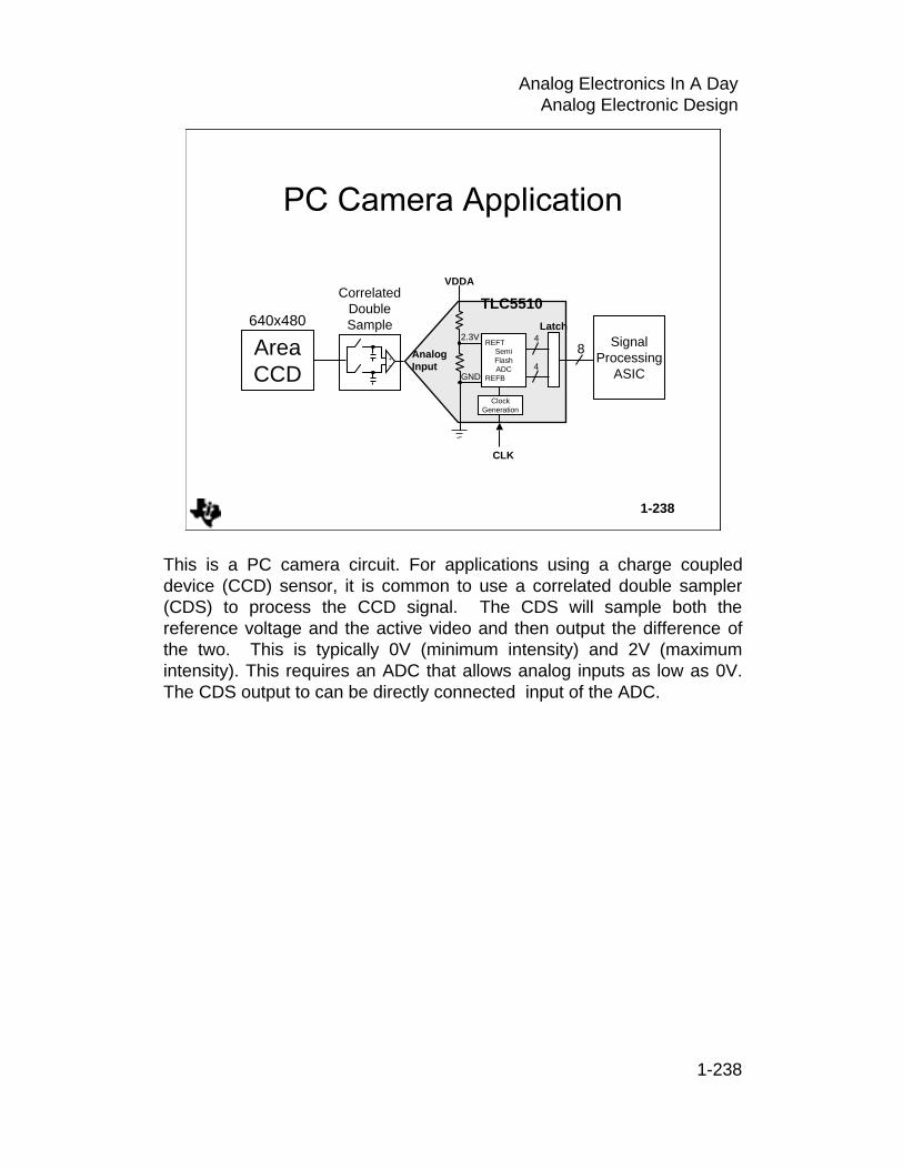
1-238
Analog Electronics In A DayAnalog Electronic Design
1-238
CorrelatedDoubleSample
-+
TLC5510
AnalogInput
8
Latch
4
4
GND
VDDA
2.3V
CLK
SignalProcessing
ASIC
640x480
AreaCCD
ClockGeneration
REFTSemiFlashADC
REFB
This is a PC camera circuit. For applications using a charge coupled device (CCD) sensor, it is common to use a correlated double sampler (CDS) to process the CCD signal. The CDS will sample both the reference voltage and the active video and then output the difference of the two. This is typically 0V (minimum intensity) and 2V (maximum intensity). This requires an ADC that allows analog inputs as low as 0V. The CDS output to can be directly connected input of the ADC.

1-239
Analog Electronics In A DayAnalog Electronic Design
1-239
• Data converters are used almost everywhere digital circuitry interfaces to the real world.
• The basic system diagram is very similar regardless of the type of converter used.

1-240
Analog Electronics In A DayAnalog Electronic Design
1-240

1-241
Analog Electronics In A DayAnalog Electronic Design
1-241
• Linear Regulator
• Charge Pump
• Switch Mode Regulator
• Which is Best?
Why talk about power supplies? Every device we have covered has power supply pins. Proper operation of any electronic circuit whether analog or digital depends on having the correct source of power.Technically a power supply consists of an energy source (battery, solar cell, AC power mains, etc.) and in most cases a regulator circuit. This section will look at linear, charge pump, and switch mode regulator circuits.
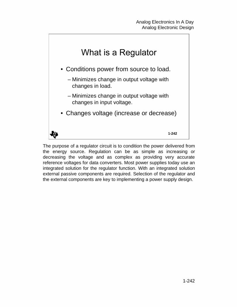
1-242
Analog Electronics In A DayAnalog Electronic Design
1-242
• Conditions power from source to load.
– Minimizes change in output voltage with changes in load.
– Minimizes change in output voltage with changes in input voltage.
• Changes voltage (increase or decrease)
The purpose of a regulator circuit is to condition the power delivered from the energy source. Regulation can be as simple as increasing or decreasing the voltage and as complex as providing very accuratereference voltages for data converters. Most power supplies today use an integrated solution for the regulator function. With an integrated solution external passive components are required. Selection of the regulator and the external components are key to implementing a power supply design.

1-243
Analog Electronics In A DayAnalog Electronic Design
1-243
– Current flow through the device is continuous– Output voltage is controlled by varying the impedance of
the pass transistor– Input voltage must be greater than the output voltage– If the input voltage gets too low, the output drops out of
regulation
RegulatedOutput
ErrorAmp
VREF
FeedbackVoltage
InputVoltage
Pass Transistor
REF SamplingElement
Linear voltage regulators are often used where the input power source is unregulated or clean supplies are required in a noisy environment, such as precision analog circuits.
The linear regulator controls the output voltage by varying the impedance of a pass element. The input voltage is always higher than the output voltage. The power that is not needed is dissipated by the pass element, i.e. converted into heat.
The output voltage is divided down with a resistive divider and compared with the reference voltage. If the output voltage is too low, the error amplifier drives the pass element more reducing it’s impedance. If the output voltage is too high the error amplifier drives the pass element a little less increasing the impedance. The output voltage is therefore regulated by the resistive divider and error amplifier.
The power dissipation of a linear regulator depends on the difference between the input and output voltage and the output current. This means a voltage regulator is only useful and efficient if the input-output differential is small compared to the output voltage.

1-244
Analog Electronics In A DayAnalog Electronic Design
1-244
– An LDO is designed to minimize the difference between the input voltage and the regulated output
A linear regulator that will operate with an input/output difference < 2V
RegulatedOutput
ErrorAmp
VREF
FeedbackVoltage
InputVoltage
Pass Transistor
REF SamplingElement
The dropout voltage is the voltage difference between input and output voltage when regulation ceases.
The dropout voltage of a regulator with a npn-transistor as pass element is very high and depends on the driver capability of the error amplifier, and is a minimum of one forward voltage of a diode. The quiescent current is not very critical because it is part of the output current. Both dropout and quiescent current can increase when the transistor aproaches saturation just prior to dropout.
In a regulator with a pnp-transistor the dropout voltage is lower, i.e. the saturation voltage of the transistor, and is independent on the driver capability of the error amplifier because the base is driven to ground. The quiescent current in such a regulator is very critical because bipolar transistors are current driven and in a regulator with a pnp pass element, the current is lost (it flows from the input to ground). Therefore, this device would also decrease the battery life quickly.
Low dropout (LDO) voltage regulators with PMOS-transistor pass elements have a dropout voltage that is proportional to the output current. The dropout voltage is dependent on the on-resistance RDSon. The quiescent current is very low (PMOS-transistors are voltage driven) and it stays low over load and input voltage. The load, line, and ripple rejection can be increased with good design techniques.

1-245
Analog Electronics In A DayAnalog Electronic Design
1-245
123456789
1011121314
2.5 V
NC 1RESETNC NC1GND NC1EN 1SENSE1IN 1OUTNC 2 RESETNC NC2GND NC2EN 2SENSE2IN 2OUT2IN 2OUTNC NCNC NC
R2 = 100kΩ
GND
C11µF
C210µF
C310µF
+
VC549DSP
Reset (Core)CVDD(Core Supply)
DVDD(I/O Supply
GND
D3DL5817
3.3 V
DL4
148
D1
D2
+
5 V
2827262524232221201918171615
DSPs often require two power supplies. The core supply furnishes power to the processor circuits. The I/O supply furnishes power just to the input/output circuitry. This scheme reduces power consumption while still allowing the processor to interface with conventional logic circuits operating at higher voltage levels.
The application shown above uses a dual LDO circuit to provide 3.3V and 2.5V from a single 5V power source. The integrated circuit contains a pass transistor, reference voltage and all control circuits necessary to implement the system. External filter capacitors are required on the input and both outputs of the LDO.
Efficiency of this circuit is:
)II(5I)3.3(I)5.2(
PP
)II(5)DVddI()CVddI(
PP
DVddCVdd
DVddCVdd
IN
OUT
DVddCVdd
DVddCVdd
IN
OUT
++=
+×+×=

1-246
Analog Electronics In A DayAnalog Electronic Design
1-246
A network of components that transfers energy from one DC level to another using capacitors. The circuit may step-up, step-down or invert the input voltage, depending on the topology
SamplingElement
REFErrorAmp
VREF
FeedbackVoltage
RegulatedOutput
Control
InputVoltage S1 S2
S3 S4C1+-
A charge pump regulator changes the output voltage by using a set of semiconductor switches and a capacitor. The capacitor serves as an energy storage device in this regulator. The circuit above operates as a voltage doubler by first closing S2 and S3. This causes current to flow through C1 storing a charge (with voltage polarity as shown). When the capacitor is sufficiently charged S2 and S3 are opened. S1 and S4 are now closed effectively adding the voltage across C1 to the supply voltage. A similar circuit can be used to generate a negative voltage by having a different switch arrangement.

1-247
Analog Electronics In A DayAnalog Electronic Design
1-247
TPS60100 steps-up 2 Cell Battery Voltage to generate low noise 3.3 V supply and 1.8V Core Voltage
2.2µF
TPS60100 Charge Pump
2 Battery Cells(e.g. Alkaline)
1.8V/77mA
10µF 22µF
4.7µF
TPS76318LDO
0.1µF
+
3.3V/110mA
2.2µF
DSP
The circuit above uses a charge pump to increase the voltage from a battery and then an LDO to create a second regulated voltage. This is an effective solution for a low power DSP. The charge pump regulator is limited in how much current that can be supplied at the output.

1-248
Analog Electronics In A DayAnalog Electronic Design
1-248
A network of components that transfers power from one DC level to another. The circuit may or may not provide isolation, and may step-up or step-down the input voltage
SamplingElement
REFErrorAmp
VREF
FeedbackVoltage
InputVoltage
RegulatedOutputFilter
The transistor used in a linear regulator works as a variable resistor that reduces the voltage by dissipating the power that is not needed.Therefore, the efficiency is low if the difference between the input and output voltage is high.
The switch-mode power supply uses a transistor switch, either fully conducting or blocking. The switch is opened and closed at a high frequency and only closed as long as needed to transfer the necessary output power. The efficiency can be very high (90 % or more). The basic system is the same. A portion of the output is sampled, compared to a reference and the result is used to control the switch operation. The switch mode regulator requires an output filter. This serves both as an energy storage device and a low pass filter for the noise. This type of circuit requires an inductor in the filter. Depending on the filter circuit this regulator can increase, decrease or invert the ouput voltage.
The advantages of a switch-mode power supply compared with a linear regulator are high efficiency, high power-to-weight ratio, and high input to output differential.
Nevertheless, there are also advantages of linear regulators. In a linear regulator the electrical noise is lower, the design of a linear regulator is less complex, and the output ripple is smaller.

1-249
Analog Electronics In A DayAnalog Electronic Design
1-249
High Input RippleLow Output RippleEfficiency Independent of VIN
Low input rippleHigh output rippleLow peak currents
Step-Down ConverterL
D CVIN VOUT
VOUT = VIN × tonton + toff
VOUT = VIN × (1 + )tontoff
Step-Up ConverterL D
CVIN VOUT
Switch-Mode Regulator Topologies
There are four different basic switch mode power supply topologies.
Switch-mode supplies are controlled by the opening and closing of a switch.
Making the output voltage a function of ton and toff .
ton: time where current flows through the switch
toff: time where current flows through the diode (continuous-mode only)
Step-Down Converter (also called Buck Converter)
When the switching element is closed, current flows through the inductor. When the switch is open the energy stored in the inductor maintains the current flow to the load and the charge on the capacitor.
Compared with the other three basic topologies the output ripple is the lowest because of the location of the inductor. This makes it appropriate for noise-sensitive loads. The disadvantages of this topology are that theswitch has to be a PMOS-transistor or a floating drive must be used for the switch and usually there is a need for a significant input EMI filter.

1-250
Analog Electronics In A DayAnalog Electronic Design
Step-Up Converter (also called Boost Converter)
When the switching element is closed, current flows only into the inductor. When the switch opens the energy stored in the inductor plus the input voltage flows to the load and charges the capacitor.
The output ripple of this topology is relatively high. A step-up converter is very useful for low input voltages or low power applications, for example in battery-driven systems where some devices need 5-V supply voltage. The biggest disadvantage of this topology is the high output voltage ripple because the output capacitor has to supply the entire load during the transistor on-time.

1-251
Analog Electronics In A DayAnalog Electronic Design
1-251
VOUT = - VINHigh output rippleEfficiency independant of VIN
High output rippleSensitive to load changesHigh peak output currents
Inverter
L
D
C VOUTVIN
VOUT = - VIN ×tontoff
Flyback ConverterD
L CVIN VOUT
VOUT = VIN × × tontoff
1a
Inverter (also called Buck-Boost Converter)
When the switching element is closed, current flows into the inductor. When the switch opens the diode-inductor junction goes negative and the energy stored in the inductor flows into the load and charges the capacitor.
The output ripple is also high because the output capacitor has to supply the entire load during one portion of the switching cycle. Some battery driven systems like mobile phones need a negative voltage to supply some RF amplifiers.
Flyback Converter
When the switching element is closed, current charges the first inductor. When the switch is open the energy stored in the first inductor is transferred to the second inductor and then to the load and capacitor.
The output ripple is high because, during the on-time the output current is supplied entirely by the output capacitor. This converter can be used in a computer where the supply voltage needs to be decoupled from the net supply and the input voltage needs to be transformed down from, say, 24V to 3V or 5V. This sort of switch mode power supply is normally only used where the space needed for the inductor (transformer) is not a limiting factor.

1-252
Analog Electronics In A DayAnalog Electronic Design
1-252
…Which one is best?
Linear Regulator Advantages– Simple low-cost design– Uses few external components; less
board space required
– No switching noise; low output ripple
and Disadvantages– Use only to generate a lower voltage– Poor efficiency: % Efficiency =
Vout/Vin
– Power dissipation may be a concern
Linear Regulator is best when– Vin - Vout is small– Low-to-medium current
applications– Low output ripple is important
Switching Regulator Advantages– Good for voltage increase,
decrease or inverting– High efficiency, 70% to 95%
– Lower power dissipation
and Disadvantages– More complex and costly design– High output ripple
Switching Regulator is best when– Large Input-to output difference– Medium-to-high current
applications – Efficiency is important– Voltage needs to be increase or
inverted

1-253
Analog Electronics In A DayAnalog Electronic Design

1-254
Analog Electronics In A DayAnalog Electronic Design
1-254