rl78/g1f group application note 6-step control of bldc by comparator … · 2016-03-19 · rl78/g1f...
TRANSCRIPT

APPLICATION NOTE
R30AN0227EU0100 Rev.1.00 Page 1 of 30
Oct 22, 2015
RL78/G1F Group 6-Step Control of BLDC by Comparator Zero-cross detection
Introduction
This application note provides a 6-step method (120° conduction pattern) that uses a single comparator to detect the Zero-crossing on a Permanent Magnet brushless 3 phase motor. Through the use of hardware resistor divider network and comparator enhancement hardware internal to the RL78/G1F, this method reduces the amount of processing required by the MCU to detect the BEMF Zero-cross versus the Zero-cross detection by ADC method.
Target Device
RL78/G1F, 64 pin version (R5F11BLE)
R30AN0227EU0100Rev.1.00
Oct 22, 2015

RL78/G1F Group 6-Step Control of BLDC by Comparator Zero-cross detection
R30AN0227EU0100 Rev.1.00 Page 2 of 30
Oct 22, 2015
Contents
1. Overview ........................................................................................................................... 3
1.1 Development environment ....................................................................................................... 3
2. System overview .............................................................................................................. 4
2.1 Hardware configuration............................................................................................................ 4
2.2 BEMF Detection Signals ........................................................................................................... 5
3. BEMF Comparator Operation .......................................................................................... 9
3.1 Modulation Method ................................................................................................................... 9
3.2 BEMF Window ........................................................................................................................... 9
3.3 Comparator Input Multiplexing .............................................................................................. 11
3.4 TimerRD TAU trigger Multiplexing ........................................................................................ 12
3.5 TAU timer allocation ............................................................................................................... 12
4. Controlling Program Description ................................................................................. 13
4.1 System States ......................................................................................................................... 13
4.2 Motor States ............................................................................................................................ 14
4.3 6-step state machine .............................................................................................................. 16
4.4 CMP Mode Operation ............................................................................................................. 18
4.5 Phase Advance ....................................................................................................................... 20
5. Miscellaneous Operations related to Motor Control ................................................... 21
5.1 Speed Measurement ............................................................................................................... 21
5.2 Speed Control ......................................................................................................................... 21
5.3 Over-current (INTP0 operation for this app note)................................................................. 21
6. Demo Project .................................................................................................................. 22
6.1 Importing and Building .......................................................................................................... 22
6.2 Tips and Tricks ....................................................................................................................... 23
7. References ...................................................................................................................... 25
8. Appendix A ..................................................................................................................... 26
8.1 Block Wound BEMF ................................................................................................................ 26
8.2 Glossary .................................................................................................................................. 26
Website and Support ............................................................................................................. 27
Revision History ................................................................................................................... A1
General Precautions in the Handling of MPU/MCU Products........................................... A2

RL78/G1F Group 6-Step Control of BLDC by Comparator Zero-cross detection
R30AN0227EU0100 Rev.1.00 Page 3 of 30
Oct 22, 2015
1. Overview
This application note provides the theory and accompanying demo program for a brushless DC motor (BLDC) using the RL78/G1F microcontroller, including the proper use of the library of the development support tool, In Circuit Scope (Note 2). The demo program will be described from an “Abstract level”, and the reader is referred to the C project files and the Doxygen folder within the project for code documentation. The app note will focus more on the more on the theory of operation and the RL78/G1F features which allow the implementation.
In this application note, wherever possible, we will use actual scope shots (or DSO data) rather than simulated or mathematically created data.
NOTE: Although this Application note was verified with a block wound motor it should operate with a sinusoidal wound PMSM motor.
Operation checking device
Operations of the sample programs have been checked by using the following device.
- RL78G1F (R5F11BLE)
Target sample programs
The target sample programs of this application note are as follows.
(1) RL78G1F_CMP_BEMF 6-step for RL78G1F (R5F11BE) for T2001 Inverter
(Complementary PWM Positive Side, GPIO Negative Side, see section 3.1 for details)
1.1 Development environment Table 1-1 shows development environment of the sample programs explained in this application note.
Table 1-1 Development Environment of the Sample Programs
Sample
software MCU Inverter board Motor
E2studio version
Tool Chain
Low-
voltage
version
(1) R5F11BLE T2001 Note 1 BLU063S-24V-
32000 Note 3,4 V4.00.00.26
IAR for RL78
V1.40
For purchase and technical support of the low-voltage inverter board T2001, contact Sales representatives and dealers of Renesas Electronics Corporation.
Notes:
1. T2001 is a product of Desk Top Laboratories Inc.
2. The development support tool In Circuit Scope is a product of Desk Top Laboratories Inc.
Desk Top Laboratories Inc. (http://www.desktoplab.co.jp/)
3. Anaheim Motor (http://www.anaheimautomation.com/ )
4. Motor Sample signals actually taken from an “off-the-shelf” BLDC power tool motor.
RL78/G1F Group 6-Step Control of BLDC by Comparator Zero-cross detection
R30AN0227EU0100 Rev.1.00 Page 4 of 30
Oct 22, 2015
2. System overview
Overview of this system is explained below.
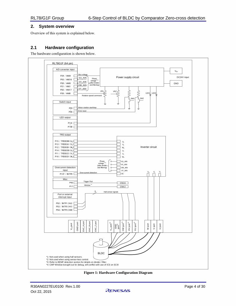
2.1 Hardware configuration The hardware configuration is shown below.
RL78G1F (64 pin)
A/D converter input
Bus voltage
Rotation speed command
TRD output
Over-current detection
Port or external interrupt input
Vdc
GND
Power supply circuit DC24V input
U p
ort
W p
ort
V p
ort
HU
po
rt*2
HW
po
rt*2
HV
por
t*2
GN
Dpo
rt*2
Vcc
po
rt*2
3
VR1 VR2*
SW1 SW2
Switch input
Motor rotation start/stop
Error reset
LED output
LED1 LED2
Overcurrent detection input
Up
Vp
Wp
Vn
Un
Wn
Inverter circuit
OCVuVvVw
Hall sensor signals
EN
C_Z
po
rt
EN
C_
A p
ort
EN
C_
B p
ort
GN
D p
ort
Vcc
po
rt
BLDC*1: Not used when using hall sensors.*2: Not used when using sensor-less control.*3: Refer to BEMF detection section for details on divider / filter.*4: CMP Window borught out for debug, will conflict with use of ICS on SCI0
VU_AIN
VV_AIN
VW_AIN
VU_AIN
VV_AIN
VW_AIN
Phase voltage*1*3
(after divider and filtering)
P24 / ANI4
P26 / ANI6
P20 / ANI0
P03 / ANI16
P21 / ANI1
P05
P06
P141
P140
P15 / TRDIOB0 (Up)
P13 / TRDIOA1 (Vp)
P12 / TRDIOB1 (Wp)
P14 / TRDIOD0 (Un)
P11 / TRDIOC1 (Vn)
P10 / TRDIOD1 (Wn)
P137 / INTP0
P52 / INTP1 (HU)
P53 / INTP2 (HV)
P54 / INTP3 (HW)
Phase voltage*1*3
(after divider and filtering)
P02 / ANI17VY_AIN
VY_AIN
Misc
P42 CN1:6Trigger Port
P17 CN4:2Window *4
Figure 1: Hardware Configuration Diagram

RL78/G1F Group 6-Step Control of BLDC by Comparator Zero-cross detection
R30AN0227EU0100 Rev.1.00 Page 5 of 30
Oct 22, 2015
2.2 BEMF Detection Signals
2.2.1 Signal Levels We need to connect the Motor Winding drive circuits back into the ADC and Comparator inputs. In addition, for the
comparator method we need to create a “virtual neutral” to compare against to find the zero-cross. You can see from Figure 2 that we need to divide from VBus (in this case about 24V) down to a 0 to AVCC range. In addition, we can note from this several important points:
BEMF goes below 0V
BEMF visible only during PWM active time
Zero-cross (Zero BEMF voltage) will occur at ½ of the motor drive signal or ½ VBus
Figure 2: Theoretical BEMF on true Motor Signals
So from this we can deduce that we should make sure:
our divider does bias up the signals to avoid negative voltages
bias up the signal to make sure the Zero-cross does not disappear below the 0V signal level
that we detect BEMF only during active PWM time.
NOTE: Since we are attempting to show true data, an actual picture of block wound BEMF may be found in section 8.1

RL78/G1F Group 6-Step Control of BLDC by Comparator Zero-cross detection
R30AN0227EU0100 Rev.1.00 Page 6 of 30
Oct 22, 2015
2.2.2 Divider Networks Fundamentally we need to get the signals down to a level acceptable by the MCU, and in addition, they need to “cross-over” at the Zero-cross so as to trigger the comparator interrupt. We will discuss the actual hardware method for doing this in section 3 but for now let’s look at the analog aspects of this problem.
Figure 3 shows the divider network for the Motor Terminals. We can determine with simple Ohms law the divider rate for these. The math is not shown here, but the relationship with VNEUTRAL (VY_AIN on the block diagram) will be discussed later in this section.
Figure 3: Motor Winding Divider and Filter
Figure 4 shows the divider and filter for the VNEUTRAL. You will note one things, the values create a 1/3 divider for the summed voltage on the 3 motor windings while maintain the bias point. This will cause a 1/3 slope on the VNEUTRAL node which sets up the perfect signal for a zero-cross detection in the comparator.
Figure 4: VNEUTRAL network
You will also note, that the filters on these networks are not very “strong”. It is intended to provide High-frequency noise reduction (i.e. inverter switching noise) while not causing large phase delays which may keep the motor from running at low-duty cycles or highest speeds. We will discuss “windowing” the comparator in a later section.
DESIGN NOTE: Since the 1/3 R value may not be a standard value, R11 and R15 are sometimes achieved by placing 3 resistors in parallel that match the dividers on the motor phases. Since they are the same value and typically from the same lot (on a reel), the accuracy of the 1/3 division ratio is almost guaranteed.

RL78/G1F Group 6-Step Control of BLDC by Comparator Zero-cross detection
R30AN0227EU0100 Rev.1.00 Page 7 of 30
Oct 22, 2015
Looking at Figure 5, we can see the resulting signals from these R-Networks as delivered to the ADC/analog inputs to the MCU.
Figure 5: Analog Motor Signals
A couple of important things to note, the “virtual neutral” slope is about 1/3 of the Motor winding signals. This means at the zero-cross, the comparator will switch making it easy to use an interrupt to signal Zero-Cross and take the appropriate action.
Also note that they swap “polarity” when comparing rising edge to falling edge (i.e. on rising motor rises above neutral and on falling motor signal falls below neutral), therefore if we want the interrupt edge to be consistent, we need some mechanism to swap the comparator inputs. This will be discussed in section 3.3.
RL78/G1F Group 6-Step Control of BLDC by Comparator Zero-cross detection
R30AN0227EU0100 Rev.1.00 Page 8 of 30
Oct 22, 2015
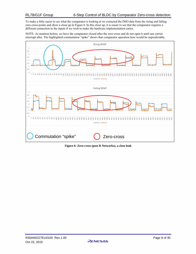
To make a little easier to see what the comparator is looking at we extracted the DSO data from the rising and falling zero-cross points and show a close up in Figure 6. In this close up, it is easier to see that the comparator requires a different connection to the inputs if we wish to make the hardware implementation easier.
NOTE: As mention before, we have the comparator closed after the zero-cross and do not open it until one carrier interrupt after. The highlighted commutation “spike” shows that comparator operation here would be unpredictable.
Figure 6: Zero-cross (post R Networks), a close look
0
0.5
1
1.5
2
2.5
3
3.5
4
1 8
15
22
29
36
43
50
57
64
71
78
85
92
99
106
113
120
127
134
141
148
155
162
169
176
183
190
197
204
211
218
225
232
239
246
253
260
267
274
281
288
295
302
309
316
323
330
337
344
351
358
365
372
379
386
393
400
407
414
421
428
435
442
449
456
Rising BEMF
Vn Vu
0
0.5
1
1.5
2
2.5
3
3.5
4
1
10
19
28
37
46
55
64
73
82
91
100
109
118
127
136
145
154
163
172
181
190
199
208
217
226
235
244
253
262
271
280
289
298
307
316
325
334
343
352
361
370
379
388
397
406
415
424
433
442
451
460
469
478
487
496
505
514
523
532
541
550
Falling BEMF
Vn Vv
Commutation “spike” Zero-cross

RL78/G1F Group 6-Step Control of BLDC by Comparator Zero-cross detection
R30AN0227EU0100 Rev.1.00 Page 9 of 30
Oct 22, 2015
3. BEMF Comparator Operation
We now have the correct analog signals that we can feed into our comparator, so we need to create of the following conditions:
Only look at the BEMF at the correct time - comparator windowing
Have the comparator inputs correctly assigned, (correct setting for + and – inputs)
3.1 Modulation Method Figure 5 shows that the BEMF is only visible during the active part of the PWM cycle, so we need to understand the modulation method being used, at least from the standpoint of “active” time, and when we can open the Comparator Window (see Figure 7).
In this demonstration, we will use complementary drive on the “positive” side of the motor and GPIO on the negative side of the motor. This provides:
a defined signal for triggering “Window” timer (one-shot gating comparator)
low-side drive always on during the step, so sampling “shunt” current is a little bit simpler.
PWM rotates among the signals to “level” the switching losses in the power devices.
active rectification of positive side drive (i.e. fly-back goes through MOSFET instead of recovery diodes)
Figure 7 shows the 6 STEPs of modulation, you can see the PWM modulating the positive side of the motor.
Figure 7: Modulation Diagram (active high drive)
3.2 BEMF Window To generate the “window” that can open and close at the correct times, a “one-shot” is the perfect solution. In this case since we want to look only during the “Active portion” of the PWM cycle, the high side of the signal modulating the Inverter should be used as the “trigger”. Since the motor may be running at very short duty cycles or very long duty cycles, this needs to happen in hardware as any software delay in this window cannot be tolerated.

RL78/G1F Group 6-Step Control of BLDC by Comparator Zero-cross detection
R30AN0227EU0100 Rev.1.00 Page 10 of 30
Oct 22, 2015
Figure 8 shows the timer window trigger and duration relationship to the PWM. When the code is running, this “window pulse” is available on P17 (see Figure 1) NOTE: The values are calculated at the time the duty cycle is calculated.
Figure 8: Compare Window Example
The delay is calculated to “open” the window away from the switching edge of the inverter where there is likely to be a lot of switching noise. Likewise the pulse width is calculated to “close” the window before the falling edge, again where there is likely to be a lot of switching noise. We use the ADC trigger point to “balance” the BEMF readings on rising and falling to get the rotor and commutation “in sync”.
NOTE: Both a Minimum Window to account for ADC Sampling and a Maximum Window so window does not stay open past end of PWM ( 95% duty – Dead-time) are defined.

RL78/G1F Group 6-Step Control of BLDC by Comparator Zero-cross detection
R30AN0227EU0100 Rev.1.00 Page 11 of 30
Oct 22, 2015
3.3 Comparator Input Multiplexing In order for all this to work, the RL78/G1F must provide a mechanism in hardware to switch the analog inputs to both the ADC and the comparator. In addition, it must be able to switch the input of the timer used for the “window” generation to be switched to the proper PWM signal that defines the high side of the modulated channel.
First let’s look at CMP1, which has the extra support for using this “window” mechanism.
Figure 9 shows both the multiplexing for the Analog inputs and the CMP Window “gate”. Since we have a multiplexer on each input of the comparator we can effectively “swap” the “+” and “-“ inputs. The analog inputs for this functionality are “hard” defined by the input pins. If you intend to use the CMP Zero-cross method, these analog channels should be assigned first in your design per this application note.
We can also see that Channel 2 of the TAU is dedicated to this “compare gating” function. This hard defines the “slave” of the one-shot pair in TAU for our “window” generation.
Figure 9: Analog Mux and Compare Gate

RL78/G1F Group 6-Step Control of BLDC by Comparator Zero-cross detection
R30AN0227EU0100 Rev.1.00 Page 12 of 30
Oct 22, 2015
3.4 TimerRD TAU trigger Multiplexing Figure 10 shows the multiplexing provided on the RL78/G1f on TAU channel 0 to allow the various PWM signals of TimerRD to be the trigger. So this allows TAU channel 2 to be the Master of a Master/Slave pair of a “one-shot”.
Figure 10: TAU / TimerRD signal multiplexing
One final note, the CMP Window we generate can be routed through the ELC and be used for other things. For example, when making the transition from Open-loop to CMP BEMF mode, we will use it to trigger the ADC and balance the rising and falling BEMF before transitioning. Please see section 4.2 MTR_OPEN_LOOP and Threshold for more details.
3.5 TAU timer allocation Since the hardware featured in the RL78/G1F define the timer pairs used for Comparator BEMF detection, the TAU timers are allocated as follows:
TAU channel 0 and 2 paired as a MASTER/SLAVE to implement the one-shot for CMP windowing
TAU channel 1 is a free running timer for doing speed measurement
TAU channel 3 is used for the commutation timer
NOTE: The speed measurement can be moved to TimerRX on the RL78/G1F if the TAU channel is needed by other tasks.

RL78/G1F Group 6-Step Control of BLDC by Comparator Zero-cross detection
R30AN0227EU0100 Rev.1.00 Page 13 of 30
Oct 22, 2015
4. Controlling Program Description
In this section we will give an abstract view of the motor control program. For details on the program the reader is referred to the Doxygen output folder (index.html) for code structure, variables, definitions, and call/caller details.
4.1 System States Figure 11 shows the system states as defined by a call to the Motor Event Function (R_MTR_ExecEvent()) and the events it can be called with.
Figure 11: Motor Event States
A call to the function R_MTR_ExecEvent() also makes an indirect (function table) call to the default actions required by the transition into the new state.
For example, a MTR_EVENT_ERROR could be any number of items that indicate the motor or the system is not in a condition to run properly, including but not limited to Over-voltage on the VBus, Over-current while motor is running, and Over-speed.
MTR_STOP
MTR_ERROR MTR_RUNEvent = MTR_EVENT_ERROR

RL78/G1F Group 6-Step Control of BLDC by Comparator Zero-cross detection
R30AN0227EU0100 Rev.1.00 Page 14 of 30
Oct 22, 2015
4.2 Motor States Figure 12 shows the motor states for this algorithm. The motor state transition are caused by various values and events within the system as the motor runs, stalls, etc.
Figure 12: Motor State Diagram
Motor State transitions are a little harder to track, so a brief description of each.
MTR_INIT_POS: This is the starting state for the Motor operation. It is here after a MTR_EVENT_RESET. It remains here until the System State goes to the MTR_RUN mode at which time this state determines the initial position of the rotor. In the case of this Demo, we use an alignment procedure (see Figure 14 for detail). Once the initial position of the rotor is determined without an error, it transitions to the OPEN Loop state.
MTR_OPEN_LOOP: In this state, the motor starts a pre-determined profile to spin the motor to a given RPM. During this period, it uses a hardware trigger (see Figure 8 ) to read and average both the rising and falling BEMF of the motor by sampling the un-driven winding of the motor. Once the BEMF is balanced and we are at an RPM that can create enough BEMF for the Comparator to detect zero-cross, the Motor moves to the MTR_CMP_BEMF mode.
We know we can only see the BEMF during active PWM, and BEMF will be stable somewhere in the center of the commutation cycle. During the open-loop commutation, we sample 4 readings in the center of the 120 degrees conduction on the non-driven winding. When the BEMF is balanced we know we our commutation is “in-sync” with the moving rotor. Figure 13 shows the BEMF values from the ADC when we are “balanced” on the rising and falling BEMF on the undriven motor terminal.
MTR_INIT_POS
MTR_OPEN_LOOP
MTR_CMP_BEMF
MTR RUN && BEMF BALANCED && RPM==transition RPM
MTR_STOP ||EVENT_RESET
MTR_STOP ||EVENT_RESET
MTR_STOP ||EVENT_RESET
MTR RUN && Position Found

RL78/G1F Group 6-Step Control of BLDC by Comparator Zero-cross detection
R30AN0227EU0100 Rev.1.00 Page 15 of 30
Oct 22, 2015
Figure 13: Balanced BEMF and Threshold
MTR_CMP_BEMF: The motor stays here until a MTR_STOP event or a MTR_EVENT RESET. Stop is usually done by a commanded RPM of 0 or SW1 turned off. EVENT_RESET can be caused by any number of dynamic events, but most common is over-current.
0
100
200
300
400
500
600
1
13
25
37
49
61
73
85
97
109
121
133
145
157
169
181
193
205
217
229
241
253
265
277
289
301
313
325
337
349
361
373
385
397
409
421
433
445
457
469
481
493
505
raw_bemf_decimal
Threshold

RL78/G1F Group 6-Step Control of BLDC by Comparator Zero-cross detection
R30AN0227EU0100 Rev.1.00 Page 16 of 30
Oct 22, 2015
4.3 6-step state machine
4.3.1 State Description Once the motor is running in either OPEN loop of Comparator mode, the commutation is a finite machine of 6 states, basically either an up or down counter depending on the direction of the motor. The state machine is given in Figure 14. The length of time in the Alignment state is empirically derived for the motor and the inertia of the load.
We align so that STEP 5 is the next state, so the next state will depend on the direction the motor will be commanded to go.
IMPORTANT: In addition to changing the pattern on the inverter pins, the commutation actually sets the inputs of the multiplexers for the comparator so it detects the correct BEMF, rising or falling. It also sets the multiplexer for the TAU trigger so we are looking at the correct PWM signal for firing the “one-shot” that opens the BEMF sampling window.
Figure 14: Motor 6-Step States Diagram
STEP 1
STEP 2
STEP 3
STEP 4
STEP 5
STEP 6
Com
mut
ate
Sig
nal &
& (
Dire
ctio
n ==
CW
)
Com
mut
ate
Sig
nal &
& (
Dire
ctio
n ==
CC
W)
ALIGN_STEP
NO STEP
(MOTOR_STATE == STOP) &&(Commanded_RPM != 0 )
if (Direction==CW)current_pos=STEP4
elsecurrent_pos=STEP6

RL78/G1F Group 6-Step Control of BLDC by Comparator Zero-cross detection
R30AN0227EU0100 Rev.1.00 Page 17 of 30
Oct 22, 2015
4.3.2 Asynchronous Commutation One of the issues when performing commutation in any BLDC/PMSM is that the BEMF zero-cross point (or HALL for sensor based algorithms) may not be in–sync with the carrier. For low-speed application, it is easy to move the commutation into sync with the carrier and live with any small error in the Speed accuracy, etc.
For a High-speed motor, this is not the case (i.e. motor commutation rate cannot possibly be an integral multiple of the carrier frequency of the PWM). For example: at 25kRPM with a 4-pole motor using a carrier of 20kHz would incur up to a 25% error if we wait for the carrier to commutate. When the zero-cross occurs and 30° has elapsed, you must commutate to avoid this.
This demo commutates using a delay timer based on the zero-cross and the speed. Therefore it will be asynchronous to the carrier and your design should be robust enough to support “runt pulses” and endure any additional switching loss due to this. Figure 15 and Figure 16 (DSO scope data plotted) provide pictures of the inverter outputs when the commutation occurs mid-PWM cycle.
Figure 15: positive-side (PWM) switching mid-cycle
37
39
41
43
45
47
49
51
53
55
57
59
61
63
65
67
69
71
73
75
77
79
81
83
85
Vn Vu Vv Vw
U: undriven driven (PWM)V: driven (PWM) undriven
Vx are the post divider signalsVn = Virtual Neutral
RL78/G1F Group 6-Step Control of BLDC by Comparator Zero-cross detection
R30AN0227EU0100 Rev.1.00 Page 18 of 30
Oct 22, 2015
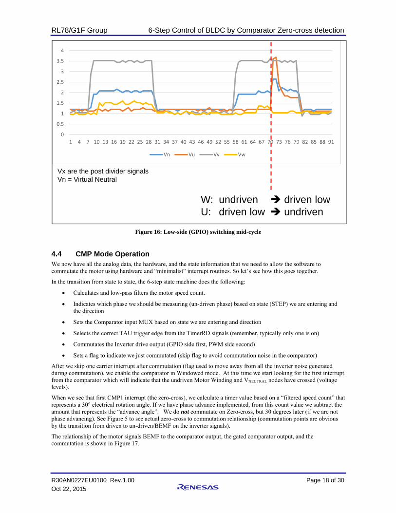
Figure 16: Low-side (GPIO) switching mid-cycle
4.4 CMP Mode Operation We now have all the analog data, the hardware, and the state information that we need to allow the software to commutate the motor using hardware and “minimalist” interrupt routines. So let’s see how this goes together.
In the transition from state to state, the 6-step state machine does the following:
Calculates and low-pass filters the motor speed count.
Indicates which phase we should be measuring (un-driven phase) based on state (STEP) we are entering and the direction
Sets the Comparator input MUX based on state we are entering and direction
Selects the correct TAU trigger edge from the TimerRD signals (remember, typically only one is on)
Commutates the Inverter drive output (GPIO side first, PWM side second)
Sets a flag to indicate we just commutated (skip flag to avoid commutation noise in the comparator)
After we skip one carrier interrupt after commutation (flag used to move away from all the inverter noise generated during commutation), we enable the comparator in Windowed mode. At this time we start looking for the first interrupt from the comparator which will indicate that the undriven Motor Winding and VNEUTRAL nodes have crossed (voltage levels).
When we see that first CMP1 interrupt (the zero-cross), we calculate a timer value based on a “filtered speed count” that represents a 30° electrical rotation angle. If we have phase advance implemented, from this count value we subtract the amount that represents the “advance angle”. We do not commutate on Zero-cross, but 30 degrees later (if we are not phase advancing). See Figure 5 to see actual zero-cross to commutation relationship (commutation points are obvious by the transition from driven to un-driven/BEMF on the inverter signals).
The relationship of the motor signals BEMF to the comparator output, the gated comparator output, and the commutation is shown in Figure 17.
0
0.5
1
1.5
2
2.5
3
3.5
4
1 4 7 10 13 16 19 22 25 28 31 34 37 40 43 46 49 52 55 58 61 64 67 70 73 76 79 82 85 88 91
Vn Vu Vv Vw
W: undriven driven lowU: driven low undriven
Vx are the post divider signalsVn = Virtual Neutral

RL78/G1F Group 6-Step Control of BLDC by Comparator Zero-cross detection
R30AN0227EU0100 Rev.1.00 Page 19 of 30
Oct 22, 2015
Figure 17: Gated compare output
So basically commutation in high-speed mode using the comparator is a function of accepting the zero-cross comparator interrupt, setting the delay timer for commutation, accepting the Delay timer interrupt and commutating which sets the hardware to repeat the process on the next CMP zero-cross detect. This requires very little CPU bandwidth. Since the commutation is asynchronous to the carrier, for speed controlled applications (not this demo), we can run the PI speed loops in the 1mS system timer tick.

RL78/G1F Group 6-Step Control of BLDC by Comparator Zero-cross detection
R30AN0227EU0100 Rev.1.00 Page 20 of 30
Oct 22, 2015
4.5 Phase Advance Earlier in the discussion about calculating the Delay timer for commutation we mentioned phase advance. We will not discuss in detail phase advance, but suffice to say it provides a method in 6-step to achieve higher RPMs in the motor, typically higher than the rated maximum speed of the motor. This puts the commutation in advance of the actual rotor mechanical position thus shifting the BEMF within the commutation period.
One of the issues with phase advance, is that this shifting of the BEMF shifts within the commutation time (see Figure 18), could be taken too far and the BEMF zero-cross could shift off so much as to be missed entirely by the hardware.
Figure 18: BEMF shifted by Phase Advance
In this particular demo, we limit the phase advance to 24 degrees maximum, but that is based on empirical testing of the asymmetry of the BEMF from the motor (i.e. BEMF is non-symmetrical in BLDC based on quality of construction, magnetism of the motor, and other factors). This is the same reason we must do some minimal low-pass filtering of the speed calculation to remove this asymmetry. The speed would jump between reading too much to be used as a “stable” reference from which to calculate or 30° commutation delay.

RL78/G1F Group 6-Step Control of BLDC by Comparator Zero-cross detection
R30AN0227EU0100 Rev.1.00 Page 21 of 30
Oct 22, 2015
5. Miscellaneous Operations related to Motor Control
5.1 Speed Measurement
5.1.1 Zero-cross to Zero-cross Since we commutate based on a fixed time (open loop) or zero-cross detection, at each commutation (step of 6 step machine), we grab the free-running timer (TAU channel 1) and subtract it from the previous reading. This gives us a delta count, and since we know the base clock, we can derive speed:
RPM = (60 * TAU clock / (6*number of pole pairs)) / Δ counter value.
5.1.2 Speed Filtering We do not need to do the speed calculation to filter for the commutation timer. We simply filter the free running counter’s delta readings. The filtering of the speed count is not very aggressive, it just needs to be enough to eliminate the jumps in the speed count value so we can get a fairly accurate 30° calculation for our commutation delay timer. In this case since we have 6 commutation cycle, we can average 8 readings and we should get rid of the jumps due to asymmetry since we will have moved greater than one full electrical cycle. In addition, by doing a power of 2, the averaging simply becomes and add and a shift, not consuming much CPU time. The raw data versus the filtered data is shown in Figure 19.
Figure 19: Raw speed counter versus Filtered speed count
5.2 Speed Control In this application we run a simple duty cycle control. This demo was intended to show applications where the operator is the “speed control loop” (i.e. variable speed tool where a trigger controls the speed). So the potentiometer in this case is acting as the trigger and we do a straight line calculation of 0-MAX_DUTY based on the trigger position.
5.3 Over-current (INTP0 operation for this app note) The demo is currently set-up to use the INTP0 signal as the overcurrent indicator. The platform that this was tested on was multi-shunt with the proper “window” comparator built onto the inverter. For a simpler implementation, the user can connect a single shunt design to the CMP0 for on chip, programmable over-current detection.
0
200
400
600
800
1000
1200
1 6 11 16 21 26 31 36 41 46 51 56 61 66 71 76 81 86 91 96
101
106
111
116
121
126
131
136
141
146
151
156
161
166
171
176
181
186
191
196
201
206
211
216
221
226
231
236
241
246
251
256
Speed_cntr Filtered_speedCntr

RL78/G1F Group 6-Step Control of BLDC by Comparator Zero-cross detection
R30AN0227EU0100 Rev.1.00 Page 22 of 30
Oct 22, 2015
6. Demo Project
6.1 Importing and Building 1) Open the e2studio workspace you want project located in
2) Use the standard Import Feature of e2studio to Import an Existing Project
3) Browse (root directory) and select the sub-directory Workspace\RL78G1F_CMP_BEMF where you unzipped the file.
4) Select RL78G1F_CMP_BEMF and FINISH.
5) If asked, Browse to your IAR install location and click APPLY, then OK
6) Project should look like Figure 20:
Figure 20: Project Explorer Panel after Import
7) Select menu Project Build All (or ).
NOTE: there may be some warnings due to the use of volatiles in the program.
RL78/G1F Group 6-Step Control of BLDC by Comparator Zero-cross detection
R30AN0227EU0100 Rev.1.00 Page 23 of 30
Oct 22, 2015
6.2 Tips and Tricks
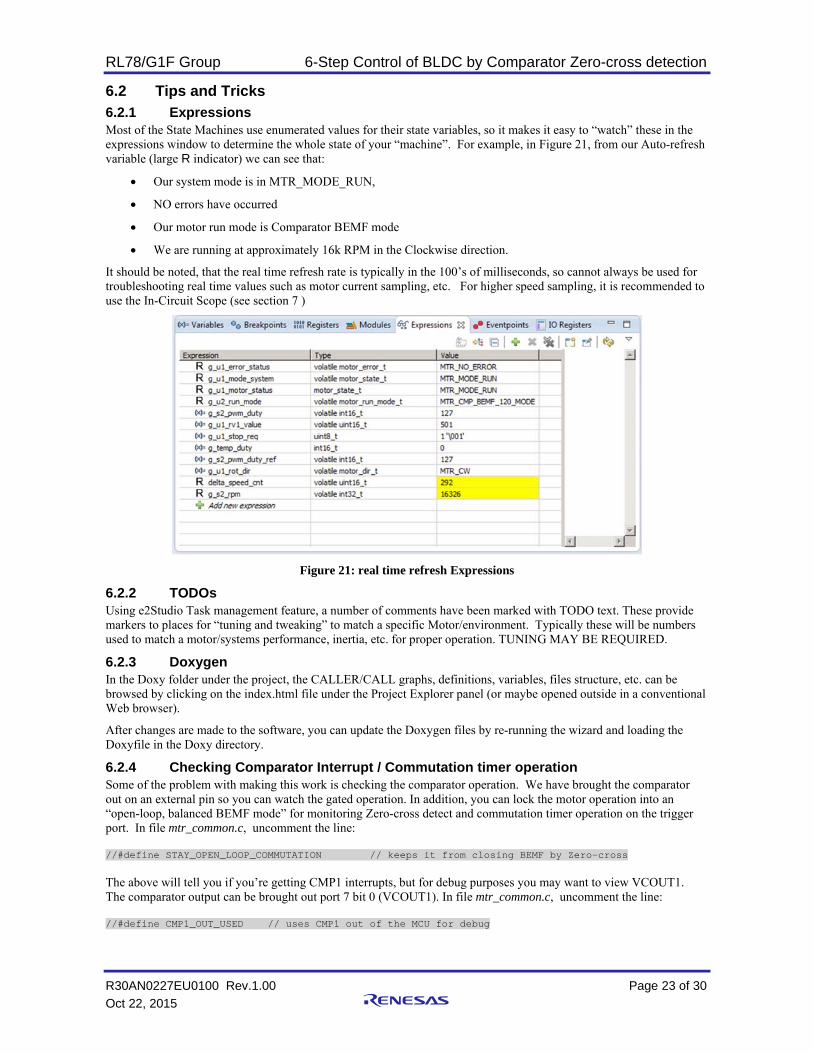
6.2.1 Expressions Most of the State Machines use enumerated values for their state variables, so it makes it easy to “watch” these in the expressions window to determine the whole state of your “machine”. For example, in Figure 21, from our Auto-refresh variable (large R indicator) we can see that:
Our system mode is in MTR_MODE_RUN,
NO errors have occurred
Our motor run mode is Comparator BEMF mode
We are running at approximately 16k RPM in the Clockwise direction.
It should be noted, that the real time refresh rate is typically in the 100’s of milliseconds, so cannot always be used for troubleshooting real time values such as motor current sampling, etc. For higher speed sampling, it is recommended to use the In-Circuit Scope (see section 7 )
Figure 21: real time refresh Expressions
6.2.2 TODOs Using e2Studio Task management feature, a number of comments have been marked with TODO text. These provide markers to places for “tuning and tweaking” to match a specific Motor/environment. Typically these will be numbers used to match a motor/systems performance, inertia, etc. for proper operation. TUNING MAY BE REQUIRED.
6.2.3 Doxygen In the Doxy folder under the project, the CALLER/CALL graphs, definitions, variables, files structure, etc. can be browsed by clicking on the index.html file under the Project Explorer panel (or maybe opened outside in a conventional Web browser).
After changes are made to the software, you can update the Doxygen files by re-running the wizard and loading the Doxyfile in the Doxy directory.
6.2.4 Checking Comparator Interrupt / Commutation timer operation Some of the problem with making this work is checking the comparator operation. We have brought the comparator out on an external pin so you can watch the gated operation. In addition, you can lock the motor operation into an “open-loop, balanced BEMF mode” for monitoring Zero-cross detect and commutation timer operation on the trigger port. In file mtr_common.c, uncomment the line: //#define STAY_OPEN_LOOP_COMMUTATION // keeps it from closing BEMF by Zero-cross The above will tell you if you’re getting CMP1 interrupts, but for debug purposes you may want to view VCOUT1. The comparator output can be brought out port 7 bit 0 (VCOUT1). In file mtr_common.c, uncomment the line: //#define CMP1_OUT_USED // uses CMP1 out of the MCU for debug

RL78/G1F Group 6-Step Control of BLDC by Comparator Zero-cross detection
R30AN0227EU0100 Rev.1.00 Page 24 of 30
Oct 22, 2015
6.2.5 An overall Signal view Once your algorithm appears to be running, you can hook up an MSO and monitor the various test points for correct operation. Figure 22 shows a sample of the TRIGGER test point, the gated CMP1 output (VCOUT1), the Comparator Time Window created by TAU, and the 4 analog signals created by the resistor networks (VU, VV, VW and VNEUTRAL).
Figure 22: Mixed Signal Sample, Motor running

RL78/G1F Group 6-Step Control of BLDC by Comparator Zero-cross detection
R30AN0227EU0100 Rev.1.00 Page 25 of 30
Oct 22, 2015
7. References
RL78G1F Group User’s Manual: Hardware (R01UH0516EJ0050)
R01AN2657EJ0100 - Application note: ‘120-degree conducting control of permanent magnetic synchronous motor: algorithm’
Applilet for RL78/G14 V1.01.01, used for sample TAU one-shot code generation
In Circuit Scope Manual
o Downloadable from: http://www.desktoplab.co.jp/download.html
o Trial series “T2001” 50W 60VA Low Voltage Inverter Unit User’s Manual

RL78/G1F Group 6-Step Control of BLDC by Comparator Zero-cross detection
R30AN0227EU0100 Rev.1.00 Page 26 of 30
Oct 22, 2015
8. Appendix A
8.1 Block Wound BEMF Figure 23 shows the actual BEMF from a block wound motor measure by constructing a “virtual neutral” with Y-connected load resistors and spinning the motor with another motor. Notice the “flat tops”, indicative of block winding.
Figure 23: Block wound BEMF
8.2 Glossary BEMF – Back Electromotive Force
BLDC Motor – brushless DC motor (typically requires electronic commutation)
DSO – Digital Signal Oscilloscope
MSO – Mixed Signal Oscilloscope
PWM - Pulse Width Modulation
TAU – Timer Array Unit

RL78/G1F Group 6-Step Control of BLDC by Comparator Zero-cross detection
R30AN0227EU0100 Rev.1.00 Page 27 of 30
Oct 22, 2015
Website and Support
Renesas Electronics Website http://www.renesas.com/
Inquiries
http://www.renesas.com/contact/
All trademarks and registered trademarks are the property of their respective owners.

A-1
Revision History
Rev. Date Description Page Summary
1.0 10/22/2015 Initial Release

General Precautions in the Handling of MPU/MCU Products The following usage notes are applicable to all MPU/MCU products from Renesas. For detailed usage notes on the products covered by this document, refer to the relevant sections of the document as well as any technical updates that have been issued for the products.
1. Handling of Unused Pins
Handle unused pins in accordance with the directions given under Handling of Unused Pins in the manual.
The input pins of CMOS products are generally in the high-impedance state. In operation with an unused pin in the open-circuit state, extra electromagnetic noise is induced in the vicinity of LSI, an associated shoot-through current flows internally, and malfunctions occur due to the false recognition of the pin state as an input signal become possible. Unused pins should be handled as described under Handling of Unused Pins in the manual.
2. Processing at Power-on
The state of the product is undefined at the moment when power is supplied.
The states of internal circuits in the LSI are indeterminate and the states of register settings and pins are undefined at the moment when power is supplied. In a finished product where the reset signal is applied to the external reset pin, the states of pins are not guaranteed from the moment when power is supplied until the reset process is completed. In a similar way, the states of pins in a product that is reset by an on-chip power-on reset function are not guaranteed from the moment when power is supplied until the power reaches the level at which resetting has been specified.
3. Prohibition of Access to Reserved Addresses
Access to reserved addresses is prohibited.
The reserved addresses are provided for the possible future expansion of functions. Do not access these addresses; the correct operation of LSI is not guaranteed if they are accessed.
4. Clock Signals
After applying a reset, only release the reset line after the operating clock signal has become stable. When switching the clock signal during program execution, wait until the target clock signal has stabilized.
When the clock signal is generated with an external resonator (or from an external oscillator) during a reset, ensure that the reset line is only released after full stabilization of the clock signal. Moreover, when switching to a clock signal produced with an external resonator (or by an external oscillator) while program execution is in progress, wait until the target clock signal is stable.
5. Differences between Products
Before changing from one product to another, i.e. to a product with a different part number, confirm that the change will not lead to problems.
The characteristics of an MPU or MCU in the same group but having a different part number may differ in terms of the internal memory capacity, layout pattern, and other factors, which can affect the ranges of electrical characteristics, such as characteristic values, operating margins, immunity to noise, and amount of radiated noise. When changing to a product with a different part number, implement a system-evaluation test for the given product.

Notice1. Descriptions of circuits, software and other related information in this document are provided only to illustrate the operation of semiconductor products and application examples. You are fully responsible for
the incorporation of these circuits, software, and information in the design of your equipment. Renesas Electronics assumes no responsibility for any losses incurred by you or third parties arising from the
use of these circuits, software, or information.
2. Renesas Electronics has used reasonable care in preparing the information included in this document, but Renesas Electronics does not warrant that such information is error free. Renesas Electronics
assumes no liability whatsoever for any damages incurred by you resulting from errors in or omissions from the information included herein.
3. Renesas Electronics does not assume any liability for infringement of patents, copyrights, or other intellectual property rights of third parties by or arising from the use of Renesas Electronics products or
technical information described in this document. No license, express, implied or otherwise, is granted hereby under any patents, copyrights or other intellectual property rights of Renesas Electronics or
others.
4. You should not alter, modify, copy, or otherwise misappropriate any Renesas Electronics product, whether in whole or in part. Renesas Electronics assumes no responsibility for any losses incurred by you or
third parties arising from such alteration, modification, copy or otherwise misappropriation of Renesas Electronics product.
5. Renesas Electronics products are classified according to the following two quality grades: "Standard" and "High Quality". The recommended applications for each Renesas Electronics product depends on
the product's quality grade, as indicated below.
"Standard": Computers; office equipment; communications equipment; test and measurement equipment; audio and visual equipment; home electronic appliances; machine tools; personal electronic
equipment; and industrial robots etc.
"High Quality": Transportation equipment (automobiles, trains, ships, etc.); traffic control systems; anti-disaster systems; anti-crime systems; and safety equipment etc.
Renesas Electronics products are neither intended nor authorized for use in products or systems that may pose a direct threat to human life or bodily injury (artificial life support devices or systems, surgical
implantations etc.), or may cause serious property damages (nuclear reactor control systems, military equipment etc.). You must check the quality grade of each Renesas Electronics product before using it
in a particular application. You may not use any Renesas Electronics product for any application for which it is not intended. Renesas Electronics shall not be in any way liable for any damages or losses
incurred by you or third parties arising from the use of any Renesas Electronics product for which the product is not intended by Renesas Electronics.
6. You should use the Renesas Electronics products described in this document within the range specified by Renesas Electronics, especially with respect to the maximum rating, operating supply voltage
range, movement power voltage range, heat radiation characteristics, installation and other product characteristics. Renesas Electronics shall have no liability for malfunctions or damages arising out of the
use of Renesas Electronics products beyond such specified ranges.
7. Although Renesas Electronics endeavors to improve the quality and reliability of its products, semiconductor products have specific characteristics such as the occurrence of failure at a certain rate and
malfunctions under certain use conditions. Further, Renesas Electronics products are not subject to radiation resistance design. Please be sure to implement safety measures to guard them against the
possibility of physical injury, and injury or damage caused by fire in the event of the failure of a Renesas Electronics product, such as safety design for hardware and software including but not limited to
redundancy, fire control and malfunction prevention, appropriate treatment for aging degradation or any other appropriate measures. Because the evaluation of microcomputer software alone is very difficult,
please evaluate the safety of the final products or systems manufactured by you.
8. Please contact a Renesas Electronics sales office for details as to environmental matters such as the environmental compatibility of each Renesas Electronics product. Please use Renesas Electronics
products in compliance with all applicable laws and regulations that regulate the inclusion or use of controlled substances, including without limitation, the EU RoHS Directive. Renesas Electronics assumes
no liability for damages or losses occurring as a result of your noncompliance with applicable laws and regulations.
9. Renesas Electronics products and technology may not be used for or incorporated into any products or systems whose manufacture, use, or sale is prohibited under any applicable domestic or foreign laws or
regulations. You should not use Renesas Electronics products or technology described in this document for any purpose relating to military applications or use by the military, including but not limited to the
development of weapons of mass destruction. When exporting the Renesas Electronics products or technology described in this document, you should comply with the applicable export control laws and
regulations and follow the procedures required by such laws and regulations.
10. It is the responsibility of the buyer or distributor of Renesas Electronics products, who distributes, disposes of, or otherwise places the product with a third party, to notify such third party in advance of the
contents and conditions set forth in this document, Renesas Electronics assumes no responsibility for any losses incurred by you or third parties as a result of unauthorized use of Renesas Electronics
products.
11. This document may not be reproduced or duplicated in any form, in whole or in part, without prior written consent of Renesas Electronics.
12. Please contact a Renesas Electronics sales office if you have any questions regarding the information contained in this document or Renesas Electronics products, or if you have any other inquiries.
(Note 1) "Renesas Electronics" as used in this document means Renesas Electronics Corporation and also includes its majority-owned subsidiaries.
(Note 2) "Renesas Electronics product(s)" means any product developed or manufactured by or for Renesas Electronics.
http://www.renesas.comRefer to "http://www.renesas.com/" for the latest and detailed information.
Renesas Electronics America Inc.2801 Scott Boulevard Santa Clara, CA 95050-2549, U.S.A.Tel: +1-408-588-6000, Fax: +1-408-588-6130
Renesas Electronics Canada Limited9251 Yonge Street, Suite 8309 Richmond Hill, Ontario Canada L4C 9T3Tel: +1-905-237-2004
Renesas Electronics Europe LimitedDukes Meadow, Millboard Road, Bourne End, Buckinghamshire, SL8 5FH, U.KTel: +44-1628-585-100, Fax: +44-1628-585-900
Renesas Electronics Europe GmbHArcadiastrasse 10, 40472 Düsseldorf, GermanyTel: +49-211-6503-0, Fax: +49-211-6503-1327
Renesas Electronics (China) Co., Ltd.Room 1709, Quantum Plaza, No.27 ZhiChunLu Haidian District, Beijing 100191, P.R.ChinaTel: +86-10-8235-1155, Fax: +86-10-8235-7679
Renesas Electronics (Shanghai) Co., Ltd.Unit 301, Tower A, Central Towers, 555 Langao Road, Putuo District, Shanghai, P. R. China 200333Tel: +86-21-2226-0888, Fax: +86-21-2226-0999
Renesas Electronics Hong Kong LimitedUnit 1601-1611, 16/F., Tower 2, Grand Century Place, 193 Prince Edward Road West, Mongkok, Kowloon, Hong KongTel: +852-2265-6688, Fax: +852 2886-9022
Renesas Electronics Taiwan Co., Ltd.13F, No. 363, Fu Shing North Road, Taipei 10543, TaiwanTel: +886-2-8175-9600, Fax: +886 2-8175-9670
Renesas Electronics Singapore Pte. Ltd.80 Bendemeer Road, Unit #06-02 Hyflux Innovation Centre, Singapore 339949Tel: +65-6213-0200, Fax: +65-6213-0300
Renesas Electronics Malaysia Sdn.Bhd.Unit 1207, Block B, Menara Amcorp, Amcorp Trade Centre, No. 18, Jln Persiaran Barat, 46050 Petaling Jaya, Selangor Darul Ehsan, MalaysiaTel: +60-3-7955-9390, Fax: +60-3-7955-9510
Renesas Electronics India Pvt. Ltd.No.777C, 100 Feet Road, HALII Stage, Indiranagar, Bangalore, IndiaTel: +91-80-67208700, Fax: +91-80-67208777
Renesas Electronics Korea Co., Ltd.12F., 234 Teheran-ro, Gangnam-Gu, Seoul, 135-080, KoreaTel: +82-2-558-3737, Fax: +82-2-558-5141
SALES OFFICES
© 2015 Renesas Electronics Corporation. All rights reserved.
Colophon 5.0