rf system in accelerator · rf system in accelerator shigeki fukuda kek, ... magnetron 40-80 high 3...
TRANSCRIPT

RF System in Accelerator
Shigeki Fukuda
KEK, Japan
2015/02/17 S. Fukuda:Indo-Japan school on Advanced Accelerators of
electron and ion 1

Introduction
RF Source Importance
• Modern Accelerator is so called “RF accelerator”, and RF is the key technology.
• Accelerator frequency is ruled by the existence of the rf source of matched frequency.
• RF system is expensive and large fraction of total cost is shared in RF source. Therefore choice of RF is very important.
• RF source is the source of failure (arcing etc.) and careful availability consideration and constant effort of maintenance are required.
2015/02/17 S. Fukuda:Indo-Japan school on Advanced Accelerators of electron and ion
2

Index
1.Introduction 2.Introduction : Accelerator and RF 3.RF Source suitable to accelerator 4.Klystron Theory 5.Klystron parameters 6.RF Source other than Klystron 7.Modulator General 8.Modulator- Line Type Modulator 9.Modulator- Other than Line Type Modulator 10. Power Distribution System 11. LLRF
2015/02/17 S. Fukuda:Indo-Japan school on Advanced Accelerators of
electron and ion 3

Early Accelerator and RF
2015/02/17 S. Fukuda:Indo-Japan school on Advanced Accelerators of electron and ion
4
Cyclotron
Simple Application of low frequency RF
Idea of linear Accelerator RF source is required. For efficient use, powerful RF Source was needed.

RF Source
Development
2015/02/17 S. Fukuda:Indo-Japan school on Advanced Accelerators of electron and ion
5
World War II forced to develop RF technology.
Stanford Mark III Linac made the klystron Power of 3-order higher in 1950’s..

Phase of RF is important Linear Accelerator (Linac)
Charged particles are accelerated linearly.
High frequency electromagnetic wave (micro-
Wave) is used for the acceleration.
Principle:
2015/02/17 S. Fukuda:Indo-Japan school on Advanced Accelerators of electron and ion
6

Variant of
Linac
2015/02/17 S. Fukuda:Indo-Japan school on Advanced Accelerators of electron and ion
7
Electron Linac
Proton Linac

RF Sources suitable for accelerator
• Factors required to accelerator rf source
1. Frequency range - higher than 0.3 GHz, klystron is best rf source. Less
than 0.3 GHz, Solid state amplifier, IOT and Tetrode are used.
2. Peak power capability -related with energy gain, short linac, and
cost benefit. How to minimize the discharge rate in tube and structures.
3. Average power capability – related with duty cycle or repetition
rate. Cw accelerator.
4. Gain – relate with driver amplifier. High gain is preferable; Generally
klystron is high gain such as 50 dB. IOT is around 20 dB. Power tetrode is poor gain.
5. Phase stability – klystron is voltage driven device and if applied voltage
is stable, phase property is excellent.
6. Simplicity, Availability and Long life – klystron is much matured
device and satisfy these requirements.
2015/02/17 S. Fukuda:Indo-Japan school on Advanced Accelerators of electron and ion
8

Available RF Sources –states of art now
Average power vs frequency plot Peak power vs frequency plot
Frequency range
Suitable for accelerator
Most available rf source for
accelerator use, klystron is
a best device for
average and peak power
capability.
Efficiency (%) Bandwidth (%)
Gain (dB)
Relative Operating
Voltage
Relative Complexity of
Operation
Gridded Tube/Diacrode 10-50 1-10 6-15 Low 3
Klystron 30-70 1-5 40-60 High 2
Magnetron 40-80 High 3
Helix TWT 20-40 30-120 30-50 High 3
Coupled Cavity TWT 20-40 5-40 30-50 High 3
Gyrotron 10-40 1 30-40 High 5
IOT 10―70 1-5 20-25 High 3
Comparison of various RF sources
2015/02/17 S. Fukuda:Indo-Japan school on Advanced Accelerators of electron and ion
9

Progress of Recent Solid State Amplifier
2015/02/17 S. Fukuda:Indo-Japan school on Advanced Accelerators of electron and ion
10
For CW use, solid-state amplifiers replace to Klystron. High efficiency is achievable. In KEK, 20-30 kW cw solid-sate amplifier (1.3GHz)is more likely candidate than IOT or Klystron for cERL.

RF Technology
1. RF Source (Klystron)
2. PS/Mpdulator
3. Waveguide
4. LLRF
2015/02/17 S. Fukuda:Indo-Japan school on Advanced Accelerators of electron and ion
11

Klystron
2015/02/17 S. Fukuda:Indo-Japan school on Advanced Accelerators of electron and ion
12

Klystron Structure and Mechanism
Key Component
of Klystron • Electron Gun
• RF Cavity
• Drift Tube
• RF Window
• Beam Collector
• Focusing Magnet
• Cooing System
Basic Mechanism of Klystron
• Electron is velocity-modulated in an input cavity.
• Then, electrons form bunch; density modulation
• Bunches are de-accelerated in an output cavity
---> beam energy to rf power
See: Inverse process of accelerator
Accelerator ----> rf power to beam energy
2015/02/17 S. Fukuda:Indo-Japan school on Advanced Accelerators of
electron and ion 13

Important parameter; Perveance
Simon's formula Definition of Perveance
Low perveance klystron has
high efficiency but applied
voltage is high.
Accelerator Laboratory, KEK
It characterize the space charge
force and deeply related with the
bunching formation and therefore
with efficiency.
2015/02/17 S. Fukuda:Indo-Japan school on Advanced Accelerators of electron and ion
14

Beam Bunching Theory
Basic Mechanism of Klystron(Linear theory) • Electron is velocity-modulated in an input cavity.
• Then, electrons form bunch; density modulation
• For this bunching mechanism, a simple linear theory is educative. There are two
approaches:
- Ballistic theory: electron which has a modulated velocity propagate without any
interaction with other electrons.
- Space-charge wave theory: entire electrons behave like a wave which is
ruled by space charge force, and automatically it contains the space charge force
effect.
More Realistic Analysis (large Signal Analysis) • For the interaction region near to output cavity, linear theory is not applicable and non
linear large signal analysis are required.
• One dimensional analysis: Disc model
• 2.5 dimensional analysis: Particle in cell Analysis including magnetic interaction
• 3 dimensional analysis: MAFIA / MAGIC code
2015/02/17 S. Fukuda:Indo-Japan school on Advanced Accelerators of electron and ion
15

Comparison of the beam trace among
two approach
Ballistic Analysis Approach
No space charge interaction
Space-charge wave approach
Space charge repulsion is included
2015/02/17 S. Fukuda:Indo-Japan school on Advanced Accelerators of electron and ion
16

More Realistic Analysis of Klystron
One dimensional disc model • Constant diameter beam is expressed as series of disc and moving as ballistic manner. • Space charge among discs is considered
• Cavity-beam interaction is properly considered.
2.5 dimensional PIC program • Electron particle in 3D • Solving under axial symmetric condition • Space-charge and magnetic field effect are included. • Realistic approach and fairly good agreement between simulation and test
2015/02/17 S. Fukuda:Indo-Japan school on Advanced Accelerators of electron and ion
17

Comment for IUAC Klystron
• IUAC needs the S-band klystron whose frequency is 2860 MHz. So far no commercial klystron coincides to the frequency.
• Due to the recent development of computer simulation, it is easy to do the special design, but quite independent design results in expensive cost.
• Miner change from existing 2856 MHz is easy and with minimum cost rise.
2015/02/17 S. Fukuda:Indo-Japan school on Advanced Accelerators of electron and ion
18

Klystron Handling
2015/02/17 S. Fukuda:Indo-Japan school on Advanced Accelerators of electron and ion
19

Klystron Window Shop
Measured performance of MBK: TH1801 Operation Frequency: 1.3GHz
Cathode Voltage: 117kV
Beam Current: 131A
mperveance: 3.27
Number of Beams: 7
Cathode loading: 5.5A/cm2
Max. RF Peak Power: 10MW
RF Pulse Duration: 1.5ms
Repetition Rate: 10Hz
RF Average Power: 150kW
Efficiency: 65%
Gain: 48.2dB
Solenoid Power: 6kW
Length: 2.5m
Lifetime (goal): ~40000h
L-Band MBK:THALES TH1801
2015/02/17 S. Fukuda:Indo-Japan school on Advanced Accelerators of electron and ion 20
S-band pule klystron: 50MW 324MHz: J-Parc
X-band PPM

Klystron Characteristics
• Child’s Law- In space charge limit current, emission current is as follows.
where is perveance, and I is current, and V is applied voltage. • Then, power is Power’s variation
• Klystron’s Impedance
Therefore, klystron’s impedance varies with applied voltage.
2/3VPI m
2/5VPVIP m
VPVP
V
I
VZ
mm
12/3
V
V
VP
VVP
P
P
m
m
2
55.2
2/5
2/3
mP
2015/02/17 S. Fukuda:Indo-Japan school on Advanced Accelerators of
electron and ion
21

Phase Variation of RF from Klystron • For linac, phase stability of RF is extreamly important
because variation dirctly reduces to energy variaion DE • Since klystron is voltage driven device and votage determine the electron
velocity, rf phase strongly depends on the voltage variation. and
– Usual S-band tube operating at 300kV range, this phase variation Is roughly 6-8 deg./(dV/V%). If you want to get DE /E=0.1%, then 0.025% of voltage flatness is required.
• Water cooling variation of tube body also causes rf phase variation. This happens since water temeperature changes the gain cavitiy‘s detuning frequency and bunch center changes from original position.
– this phase variation Is roughly 0.5-1 deg.phase/1 deg water temp.
-8
-6
-4
-2
0
2
4
6
8
10
-2 -1.5 -1 -0.5 0 0.5 1 1.5 2
Ratio of applied voltage @300kV (%)
Ph
ase (d
eg
ree)
simulation
measured
-25
-15
-5
5
15
25
-10 -5 0 5 10Dwater temperature [degree]
Do
utp
ut
ph
as
e [
de
gre
e]
free (ANSYS)
rigid (ANSYS)
Experiment
2
2
0
0
0
0
)1(
11
22
mc
eVc
L
u
L
D)
%deg
(86)( VVV DD
D
2015/02/17 S. Fukuda:Indo-Japan school on Advanced Accelerators of
electron and ion
22

Applied Voltage and power-gain relationship
2015/02/17
S. Fukuda:Indo-Japan school on
Advanced Accelerators of electron and
ion
23
0
10
20
30
40
50
60
0 50 100 150 200 250
Ou
tpu
t p
ow
er(
MW
)
Input power(W)
Applied voltage and input power vs output power
Generally higher the applied voltage, lower the saturated point is and Higher the gain is.
240kV
225kV
250kV
250kV

Electron gun and beam generation
Structure of electron gun in the klystron From the requirement of large current, electrons generated from the large aperture cathode are focused and emitted to the drift tube.
Cathode: 900-1100 deg. Thermal electrons are emitted
Beam forming electrode (BFE)
form the laminar flow
beam.
Anode: entrance to drift tube
Generally cathode is negative
and anode is o volt.
2015/02/17 S. Fukuda:Indo-Japan school on Advanced
Accelerators of electron and ion 24
Anode
BFE
Cathode

Temperature limited (TL) flow and
space-charge (SC) limited flow As cathode surface temperature getting higher due to the heater power up, thermal electrons are start to emit from the cathode surface.
• Current is described by the Richardson-Dushman’s formula.
T is absolute temperature, φ is work function of the cathode and k is the Boltzmann constant. This current emission range is called as temperature limited region(TL).
• More higher the cathode temperature is, cathode surface is filled with space charge and current does not increase as temperature is getting high.
• Emission of this range is called space charge limited region (SC).
• Emitted current is determined by the geometry of the gun and applied voltage.
• Current is proportional to power of 3/2 of the voltage. Ideal SC flow is called as FSCL: Full Space Charge Limit. Real cathode deviates slightly from FSCL.
• FSCL Emission from the parallel electrode is follows.
2015/02/17 S. Fukuda:Indo-Japan school on Advanced
Accelerators of electron and ion 25
kTeTAJ
2
0
2
2
3
0
2
9
24
z
V
m
eVJ

TL flow and SC flow
2015/02/17 S. Fukuda:Indo-Japan school on Advanced Accelerators of electron and ion
26
kTeTAJ
2
02
2
3
0
2
9
24
z
V
m
eVJ
Cu
rren
t(A
)
Applied voltage
Current vs voltage
T3
T2
T1
3/2乗
則 C
urr
ent
Cathode tempereture
Current vs cathode temperature
Cu
rren
t
Cathode
V is varied
V is constant
Higher current
Higher the voltage
SC Region TL region
SC region
TL region

Heater adjustment and the klystron life
S. Fukuda:Indo-Japan school on Advanced Accelerators of electron and ion
27
• Usually operation point is the saturated point because the current fluctuation is minimum for other parameter’s fluctuation
• Heater power setting point is important because it affects the stabilities and klystron life. From Miram plot, following way is recommended.
• Measuring 1 point on the Miram plot takes about 30 min. to reach to the
stable current. • After the long usage, due to the degradiation of thecathode, emission
decrease gradually and you must readjust the operating point.
Emis
sio
n c
urr
ent
Temperature/Heater power/heater current
Setting point of heater power
Cu
rren
t Cathode temperature
Cathode activity variation
Long operation shifts the point.
From the shoulder point, A few % higher point is Set. More high.er than it Results in the short cathode life
2015/02/17

Convenient method to measure Miram plot
DIP testing
2015/02/17 S. Fukuda:Indo-Japan school on Advanced
Accelerators of electron and ion 28
Usually it takes a long time to complete the measurement of Miram plot because at each point you must wait for the heat equilibrium. Half day per one klystron is required, and the institute having many klystrons has a difficult to have a measurement frequently. Dip testing is a convenient way to evaluate the operation point of the cathode. During the operation, quick heater off is done and the dip (decreasing amount of current) is measured. Special care is for abnormal HV in Line type modulator. Interlock off sequence is needed.

Multi-beam klystron for ILC
Toshiba
E3736H
Scope picture of the klystron test.
The lines show the klystron voltage
(116 kV) in yellow, the current
(128 A) in blue and RF output
(5 MW each) in magenta and green.
10MW 1.5ms
67% efficiency

Technology for MBK
magnetic field is curing
output waveguide for high power micro-wave
coils for beam focusing
6 electron beams from 6 thermionic cathodes
Microwave is amplified by the klystron. In klystron, microwave cavity is
used to modulate the beam velocity by small power.
Modulated beam reach to its maximum bunching
at the output cavity, and generate high power microwave.
microwave cavity to make beam velocity modulation

Important parameter; Perveance
Simon's formula Definition of Perveance
Low perveance klystron has
high efficiency but applied
voltage is high.
Accelerator Laboratory, KEK
It characterize the space charge
force and deeply related with the
bunching formation and therefore
with efficiency.
2015/02/17 S. Fukuda:Indo-Japan school on
Advanced Accelerators of electron
and ion
31

Modulator
2015/02/17 S. Fukuda:Indo-Japan school on Advanced Accelerators of electron and ion
32

Requirement to RF source from
accelerator specification
• Energy Gain E
» It depends on the accelerator final energy, and it is the SQRT of P (proportional to electric field)
• Energy width E/E should be as small as possible
» this corresponds to minimize ΔP/P and Δθ/θ.
• In order to achieve these requirements, good quality of
modulator (good stability of output pulse) is required.
2015/02/17 S. Fukuda:Indo-Japan school on Advanced Accelerators of electron and ion
33

Various Modulator
• Modulator for short pulse ( ~ microsecond order) – electron linac
• Line type modulator: most popular, low cost, simple – Pulse forming
» PFN (pulse forming network)
» Blum Line
• Hard tube pulser (Solid state amplifier) – Pulse amplifier
– Pulse generation by IGBT
• Magnetic compressor modulator
• Marx Generator
• Modulator for long pulse(~ a few hundred microseconds to a few milliseconds) – proton linac
– IGBT modulator with bouncer circuits
– Marx generator
2015/02/17 S. Fukuda:Indo-Japan school on Advanced Accelerators of
electron and ion
34

Modulator(1)
Line-type Modulator
2015/02/17 S. Fukuda:Indo-Japan school on Advanced Accelerators of electron and ion
35

Principle of Line Type Modulator
(Most popular modulator)
• Basic Circuit
• Pulse width is determined by the traveling time of the line
• Matching condition (Z0 is characteristic impedance of co-axial line)
lineoflengththeiswhereu
.2
RZ 0
2015/02/17 S. Fukuda:Indo-Japan school on Advanced Accelerators of
electron and ion
36

Line-type Pulser
2015/02/17 S. Fukuda:Indo-Japan school on Advanced Accelerators of
electron and ion
37
PFN-type modulator LC resonant charging Stability De-Qing Single thyratorn switch
Charging Circuit can be replaced by rather small inverter P/S.
Stability determined by charger

Discharging Circuit
• Cable Equivalent circuit
• Analysis of N stage pulse forming network (PFN) 1st stage
r-th stage
n-th stage
Solving this exactly is difficult and using Laplace transformation with suitable approximation or computer simulation is frequently used.
EdiiC
tiRdt
tdiL
t
))()((1
)()(
210
1
1
Open end
0))()((1
))()((1)(
10
10
dii
Cdii
Cdt
tdiL
rr
t
rr
tr
0)(1
))()((1)(
01
0
di
Cdii
Cdt
tdiL
t
nnn
tn
2015/02/17 S. Fukuda:Indo-Japan school on Advanced Accelerators of
electron and ion
38

Characteristics of PFN
• For n-stage PFN
pulse width
Characteristic impedance of PFN
Requirement of PFN-Parameter
• Klystron’s operation point Vs, Is then Zs = Vs / Is
• Step up ratio of pulse transformer n, then primary impedance is ZS = ZS / n2
• From matching condition, PFN characteristic impedance ZPFN = ZS
• Pulse width is come from Klystron’s requirement or system design.
• Total capacitance of PFN is derived
by energy equation: energy stored in
PFN=energy supplied to the load
• stage number is determined by flat top condition
nCCCnLLLwhere
LCnCL
iNiN
NN
,
22
C
L
C
LZ
N
N
PFN
2
0
2
2
2
1
C
pp
T
ppCT
V
IVCor
dtIVVC
2015/02/17 S. Fukuda:Indo-Japan school on Advanced Accelerators of electron and ion
39

PFN Simulation Example
L=1.3[mH] L2=0[H] C=0.015[mF] Stage number of PFN 1,3,5,10,20
2015/02/17 S. Fukuda:Indo-Japan school on Advanced Accelerators of electron and ion
40

• Modulator failure distribution
Total operation time : 6322 Hours
Machine failure time : 114 Hours
Operation Statistics in FY2007
•Keep-alive current tuning
•Thyratron failure
•Air cooling fan
Modulator availability=0.997
Modulator failure time = 17.6 Hours
• Linac failure distribution
53% of RF failure
Reliabilty of an RF system is directly linked to
the linac availability.
2015/02/17 S. Fukuda:Indo-Japan school on Advanced Accelerators of electron and ion
41

Status of Thyratron
Litton EEV ITT L4888B CX2410K F-241
• 45 kV, 5 kA, 6 µs, 50 Hz Switching
Operation period ( Sep. 1998〜 Feb.2008) : No. of Thyratrons=74
• Lifetime Profile • Failure Modes Distribution
Thyratron Quality ?
0
2
4
6
8
10
0 10 20 30 40 50 60 70 80
CX2410KF241L4888B
Nu
mb
er o
f T
ub
es
Time(kHours)
Driver circuit
•Keep alive has ~250 mA dc current at 100 V
• Thyratron circuit
Keep alive Failure
G1 discharge
High voltage
Break Down
Reservoir Failure
Others
2015/02/17 S. Fukuda:Indo-Japan school on Advanced
Accelerators of electron and ion 42

Matching and mismatching
• For lossless transmission line, current transformation is
• And its inverse transformation,
• Therefore, depending on , waveform is different after t=2.
• matching condition and no reflection
• mismatch (positive mismatch)
extreme case :open end
lower operation point than normal
• mismatch (negative mismatch)
extreme case :short end
pp
p
g
p
p
gg
eRZ
RZe
RZ
RZ
RZp
eV
eRZ
RZ
e
RZp
V
pZRp
Vpi
42
0
02
0
0
0
2
2
0
0
2
00
)(1)(
)1(
1
1
)()coth()(
6,4,2),(
00)(01)(
)6()4()()4()2()4()2()2(1)( 2
0
0
0
0
0
0
0
0
nntt
tfortUandtfortUwhere
tUtURZ
RZtUtU
RZ
RZtUtU
RZ
RZtU
RZ
Vti
D
DDDD
R
0ZR
0ZR
0ZR
2015/02/17 S. Fukuda:Indo-Japan school on Advanced Accelerators of electron and ion
43

Protection Circuit for load discharge etc. • If discharge occurred in klystron or pulse transformer circuit, pulse
reflection occurs due to the mismatching effects. Serious case, undesirable inverse voltage causes the failure of various devices. Therefore, protection circuit is employed in the system and it force to stop operation with a pulse or a few pulses later.
• Fast protection: End of line clipper (within a pulse response)
• Rather slow protection: reversed shunt circuit Average of inversed current due to the load discharge is sensed and stop operation by meter relay etc.
2015/02/17 S. Fukuda:Indo-Japan school on Advanced Accelerators of electron and ion
44

Parameters K2-3 Unit
RF Peak Power 30- 60 [MW]
Pulse Voltage 280 - 450 [kV]
Pulse Current 230 - 450 [A]
Modulator Peak Power 160 [MW]
Modulator Average Power 0,5 - 100 [kW]
Mains: 1-phase / 3-phase 3
Cooling Water
RF POWER UP TO 60 MW MODULATOR PEAK POWER UP TO 160 MW Pulse transformer is used to step up the voltage
Commercial Solid-state Amplifier
(Scandinova)
2015/02/17 S. Fukuda:Indo-Japan school on Advanced Accelerators of electron and
ion 45
IUAC is planning to introduce this type of modulator.

Modulator other than Line-Type
2015/02/17 S. Fukuda:Indo-Japan school on Advanced Accelerators of
electron and ion 46

Pulse Modulator Using Multi-Series Switch(1)
Series Switch
• Series Switch Modularor
Storage Capacitor PS PS
Cell Modulator
• Marx Type Modulator
• Flexible Active waveform control • Pulse waveform • Pulse flatness
2015/02/17 S. Fukuda:Indo-Japan school on Advanced Accelerators of electron
and ion 47

Series Switch Modulator
(Diversified Technologies, Inc. )
IGBT Series Switch
140kV, 500A switch shown at left in use at CPI
As a Phase II SBIR, DTI is building a 120 kV, 130 A version with a bouncer to be delivered to SLAC at the end of 2006
2015/02/17 S. Fukuda:Indo-Japan school on Advanced Accelerators of
electron and ion 48

SNS High Voltage Converter
Modulator (Unit installed at SLAC)
RECTIFIER TRANSFORMER
AND FILTERS SCR
REGULATOR SWITCHING
BOOST TRANS-
FORMER
HV RECTIFIER AND FILTER NETWORK
13.8KV
3Ø
INPUT
LINE CHOKE
5th
HARMONIC
TRAP
7th
HARMONIC
TRAP
50mH
AØ
BØ CØ
3Ø
(ON/OFF)
4mH
400A
4mH
400A
6 EACH
6 EACH
RTN AØ BØ CØ
-HV -HV -HV 10ohm 20mH
.03uF
.03uF
.05uF VMON
HV
OUTPUT
RECTIFIER TRANSFORMER
AND FILTERS
SCR REGULATOR
HVCM EQUIPMENT CONTROL RACK
ENERGY STORAGE
Other Alternative Modulators
2015/02/17 S. Fukuda:Indo-Japan school on Advanced Accelerators of
electron and ion
49

Longer Pulse Modulator with sag
compensation with RC circuit
2015/02/17 S. Fukuda:Indo-Japan school on Advanced Accelerators of
electron and ion 50

Long Pulse Modulator with Bouncer Circuit(1)
CR
t
eVV
0
Klystron Impedance
R=120kV/140A
=857Ω
C
Pulse width
C
R Dr
=1.7ms
Dr=1%
R=857Ω
Dr Droop
Secondary Capacitance C=198µF
E 1
2CVk
2
E=1.4MJ
Vk=120kV
If droop of 20% is allowed, then C
and E are 1/20
Save Capacitor bank and space
to1/20 24min run
of 1kW
heater
C=9.9µF (Secondary)
C=1426µF(Primary)
Switch
2015/02/17 S. Fukuda:Indo-Japan school on Advanced Accelerators of electron and ion
51

Long Pulse Modulator with Bouncer Circuit(2)
10kV
-120kV
140A
1.7 ms
5Hz 1.7kA
2015/02/17 S. Fukuda:Indo-Japan school on Advanced Accelerators of electron and ion
52

Accelerator Laboratory
Actual Waveform by Bouncer Circuit
Es=20kV, Pw=1.7ms, fr=5pps Rise-time(10-90%)=33µs
Es=17kV, Pw=1.7ms, fr=5pps Flatness=0.8%(p-p)
•With Bouncer Circuit
-100
-95
-90
-85
-2 -1.5 -1 -0.5 0 0.5
Kly
stro
n V
olt
age(
kV
)Time(ms)
Es=17kVfr=5pps
0.3ms
0.7ms
0.52ms
0.4ms
0.6ms
-4000
-3000
-2000
-1000
0
1000
2000
3000
4000 -140
-120
-100
-80
-60
-40
-20
0
20-3 -2 -1 0 1 2 3 4
Bounce
r V
oltag
e(V
)/C
urr
ent(
A)
Kly
stron V
oltag
e(kV
)
Time(ms)
Klystron Voltage
Bouncer Voltage
Bouncer Current
2015/02/17 S. Fukuda:Indo-Japan school on Advanced Accelerators of electron and ion
53

Protection of Klystron at Breakdown
Es=9.0 kV, Pw=1.7 ms, fr= 5 pps
W 100V Ik dt
Energy deposit in klystron
from gun spark
W=2.0 J < design value
Arc voltage=100 V
54 2015/02/17 S. Fukuda:Indo-Japan school on Advanced
Accelerators of electron and ion 54

Pulse Transformer Modulator Status
• 10 units have been built, 3 by FNAL
and 7 by industry (PPT with
components from ABB, FUG,
Poynting).
• 8 modulators are in operation.
• 10 years operation experience.
• Working towards a more cost efficient
and compact design.
• FNAL building two more, one each for
ILC and HINS programs – SLAC has
bulit switching circuits.
HVPS and Pulse Forming Unit
IGCT Stack
2015/02/17 S. Fukuda:Indo-Japan school on Advanced Accelerators of electron and ion
55

Marx Modulator for ILC
2015/02/17 S. Fukuda:Indo-Japan school on Advanced Accelerators of
electron and ion 56

2015/02/17 S. Fukuda:Indo-Japan school on Advanced Accelerators of electron and ion
57

2015/02/17 S. Fukuda:Indo-Japan school on Advanced Accelerators of
electron and ion 58
SLAC’s New Type Marx Modulator : P2

Vendor Design Marx Modulator for ILC
2015/02/17 S. Fukuda:Indo-Japan school on Advanced Accelerators of electron and ion
59
Thomson Marx Modulator: Low voltage Marx and Pulse Transformers
DTI’s Marx Modulator: 120kV Direct Pulse Generation

Marx Modulator's Feature
• Good flat top pulse when pulse duration is long such as a few millisecond.
( timing adjustment of individual Marx cell enable to make a good flat top)
• Even a direct output pulse case, acring probability in the modulater is small due to comprise of the low voltage cell’s assembly
• Fast shutoff of the output when klystron fails.
2015/02/17 S. Fukuda:Indo-Japan school on Advanced Accelerators of electron and ion
60

Power Distribution System
(Waveguide System)
2015/02/17 S. Fukuda:Indo-Japan school on Advanced Accelerators of
electron and ion 61

Layout of RF System in KEK
2015/02/17 S. Fukuda:Indo-Japan school on Advanced Accelerators of electron and ion
62
Target
e+
1 kWAmp.
System
e-
O/E
Driver
60kW S-bandKlystron
SUB DRIVE LINE(39D)
ACC
50MW S-bandKlystron
SLED
IΦA
Sector 2
SUB-BOOSTER 2
CW
571 MHz
2856MHz
Ref. Signal Generator
(FMD-30)
E/O
Sector 1 Sector 5-1
SB5-1
e-
High Power
ATT/Phase
Shifter
BuncherPrebuncher ACC Guide
Electron Gun
10kWAMP.
114 MHz
SB-B
30m5m5m
SB-A
SHB2SHB1
114
MHz571
MHz
Coaxial Lines
1 kWAmp.
System
Sector CSector BSector A
571 MHz
TriggerSystem
Optical Lines
15m
30m
80m
SB-C
40m20m
100m
100m
MR10 MHz
508 MHz
E/O
SB-1
Counter MAIN DRIVE LINE
RF System Diagram C-band Plan(example)
SUB-BOOSTER 3-1
Sector 3-1
100kW C-bandMultiplier Klystron
SUB DRIVE LINE(WG)
SLED
IΦA
ACC
50M C-bandKlystron
Sector 3-2
SB3-2
Sector 4-1
SB4-1
Sector 4-2
SB4-2
Sector 5-2
SB5-2
E/O
5712MHz
X2
Drive Line
Rectangular Waveguide System Coaxial waveguide system

Importance of Power Distribution System
• Cost of RF system is expensive, and about 1/3 of cost is PDS cost.
• Sometimes RF efficiency and capability are determined by PDS. For example, SLED (energy doubler) specifies the peak power capability.
• Fractions of the failures of linac are come from poor design of PDS.
• PDS variants
– Coaxial waveguide PDS: low peak power, low frequency
– Rectangular waveguide PDS of air, nitrogen and SF6 w/o pressurizing.
– Rectangular waveguide PDS in vacuum
– PDS with circulator for cw/longer pulse operation, feeding to standing wave cavity structure
– Vacuum window or waveguide valve to keep structure low pressure when klystron is replaced.
– Power divider system w/o changing the delivering power
– Phase shifter system or fixed length of waveguide considering the phase at cavity and beam
2015/02/17 S. Fukuda:Indo-Japan school on Advanced Accelerators of
electron and ion 63
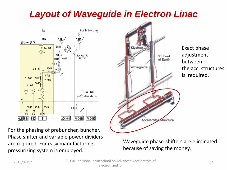
Layout of Waveguide in Electron Linac
2015/02/17 S. Fukuda:Indo-Japan school on Advanced Accelerators of electron and ion
64
Waveguide phase-shifters are eliminated because of saving the money.
Exact phase adjustment between the acc. structures is required.
For the phasing of prebuncher, buncher, Phase shifter and variable power dividers are required. For easy manufacturing, pressurizing system is employed.

2015/02/17 S. Fukuda:Indo-Japan school on Advanced Accelerators of electron and ion
65
Example of waveguide system in ILC Local PDS Layout of KCS / DKS
DKS
KCS Cross section view of tunnel and installation concept of local power distribution system
Many waveguide components including isolators are installed In atmosphere or pressurizing system.

LLRF (Low Level RF)
2015/02/17 S. Fukuda:Indo-Japan school on Advanced Accelerators of
electron and ion 66

Low level RF System
2015/02/17 S. Fukuda:Indo-Japan school on Advanced Accelerators of electron and ion
67
System includes master oscillator(MO), local oscillator(LO), timing module, down converter and digital RF controller. Pulse modulator and driver amplifier Is also included. RF protection system including slow starter of RF is in this area.

Function of LLRF • Low level RF system is the system from master oscillator to the
input rf for main klystron.
• Stable rf (frequency, power and phase) is required.
• Beam loading compensation is sometimes requested.
• Most important function of LLRF for the accelerator is a stable phase. Phasing is also important when the electron energy is changed.
• Feed forward/feed back for the output power and phase is required. Recently digital feed back is becoming more popular.
2015/02/17 S. Fukuda:Indo-Japan school on Advanced Accelerators of
electron and ion 68

Feed forward or feed back control
2015/02/17 S. Fukuda:Indo-Japan school on Advanced Accelerators of electron and ion
69
System G(s)
Input Signal U(s)
Output Signal Y(s)
System G(s)
Input Signal U(s)
Output Signal Y(s)
System H(s)
+ -
• Upper System – Its output does not change
the input signal
(Feed forward control)
• Lower System
– Parts of output signal goes back
to the input signal and input is changed.
(Closed loop control or Feedback control)
– Digital Feedback
ADC changes digital signal and then
digitally controlled. Delay time is inevitable.
Usually expensive. Easy to change.
– Analogue Feedback
No delay. Not easy to change.
Inexpensive.
ADC Digital Control
DAC
Set Data
Cavity Mod/Amp
Digital Control
Device under Control
Analogue Signal

PID Control
• PID Control is one of popular control method.
• P=proportional, I=Integral, D=derivative
• P-control feedbacks the deviation to control signal U(s), and current information is reflected.
• I-control feedbacks the integration of the deviation to U(s) and past information is reflected.
• D-control feedbacks the derivative of the deviation to U(s) and future information is reflected.
2015/02/17 S. Fukuda:Indo-Japan school on Advanced Accelerators of electron and ion
70
Deviation Controlled Object
Controller

Digital RF Controller
2015/02/17 S. Fukuda:Indo-Japan school on Advanced Accelerators of electron and ion
71
Digital controller comprises of ADC, DAC and DSP/FPGA.
DSP (Digital Signal Processor): This has a signal processor in the device and its calculation ability is powerful. Between ADC/DAC and DSP, there required the buffer device and buffer device is not synchronized with sampling signal. A few microsecond delay time is inevitable.
FPGA(Field Programmable Gate Array): Algorism of signal process is generated of numerical formula written by the hardware language. Synchronized operation with the clock signal of ADC/DAC and FPGA. Faster than DSP. Recently FPGA is becoming more popular.

Amplitude-phase and IQ control
2015/02/17 S. Fukuda:Indo-Japan school on Advanced Accelerators of electron and ion
72
Important parameter in RF is signal’s amplitude and phase. Signal from cavity is also amplitude and phase, and this means the measurement of I-component and Q-component of RF signal Using the sampling signal of IF (Intermediate Frequency), direct I and Q signals are possible to be Measured. .
amplitude
phase
Amplitude and phase measurement
IQ measurement
IQ and polar coordinate Relationship
Direct IQ measurement

Example of LLRF in KEK STF
2015/02/17 S. Fukuda:Indo-Japan school on Advanced Accelerators of electron and ion
73

Example of LLRF in KEK cERL
2015/02/17 S. Fukuda:Indo-Japan school on Advanced Accelerators of electron and ion
74

Thanks for listening my lecture
2015/02/17 S. Fukuda:Indo-Japan school on Advanced Accelerators of electron and ion
75