rf senior design project report -...
TRANSCRIPT

EEC 134 Project Report 1
RF SENIOR DESIGN PROJECT REPORT
EEC 134 Professor Xiaoquang Liu
Team DMK
Team members: Duyen Tran Khoa Huynh Michelle Lee
Date: 5/25/2016

EEC 134 Project Report 2
RF SENIOR DESIGN PROJECT REPORT Table of Contents:
Acknowledgements 1) Abstract 2) Introduction 3) Component Selection 4) Design Schematics 5) Printed Circuit Board Designs 6) Testing the System 7) Results of the Competition 8) Possibility for Future Extension 9) Suggestions for the class 10) Conclusion

EEC 134 Project Report 3
Acknowledgements
This report cannot be completed without the references of team Jame’s “Group Application Report” (School Year 201415). We try to follow their project as close as possible and we are much indebted to their explanation of the block diagram and the structure of their reports, which we follow closely. We also would like to thank professor Xiaoquang ‘Leo’ Liu and TA Hao Wang for their assistance during the two quarters to finish this project.
1. Abstract
The goal of this project was to design a frequency modulated continuous wave (FMCW) radar system that is capable of determining the distance or range of an object. The distance of an object is determined by examining the difference in frequency between the signal at the transmitter and the signal at the receiver. The operating frequency for our design is 2.4 GHz and the design is composed of two printed circuit boards, one board for the baseband and one for the RF components, as well as two can antennas. The output on board is recorded using Audacity on a laptop, which is then put through a signal processing program in Matlab to processed. From these information, the distance to the target is deduced. To test the system, three experiments are conducted at different distances on an open field, and then the accuracy is measured.
2. Introduction
The frequency modulated continuous wave radar is a short range measuring radar with the ability to measure distances, target range and its relative velocity. This FMCW radar system is capable of receiving information about the range to target through the modulation of frequency of a transmitted signal. The continuous wave varies in frequency with respect to a fixed period of time by a modulating signal such as the sawtooth, triangle, squarewave, and sinusoidal.
The frequency change is achieved by ramping up and down the voltage of the VCO in the radar transmitter. At the receiver of the radar, the difference in frequency will be observed. These differences will be used to determine the distance to an object, in this case a metal sheet.

EEC 134 Project Report 4
In this radar application, the triangle wave was chosen as the modulation pattern. As
shown above, the received signal is a delayed form of the transmitted frequency. To find the distance of objects, we first have to find the time difference of the transmitted signal from the radar to the target, for which we use the equation:
t = cd
where t is the time it takes for the transmitted signal to reach the target, d is the distance to the target, and c is the speed of light. The total time it takes for the transmitted signal to reach the target and back to the radar is given by , since it is a round trip. The frequency of the d/ct = 2 transmitter has changed by ∆f, which is related to the total time by the equation
f kΔ = × c2d
where k is the rate at which the frequency ramps up and down. can be measured by passingf Δ the received signal and the transmitted signal through a mixer. Therefore, the distance can be determined by the equation:
d = 2kc×Δf
All of the above will be implemented using a matlab code. The block diagram belows shows the structure of the FMCW radar.

EEC 134 Project Report 5
Explanation for this diagram is as followed. The triangular modulation signal is fed from the function generator into the VCO. The frequency modulated signal output from the VCO is then amplified and sent through the power splitter. The power splitter divides the signal into two channels: transmitted signal and LO reference. The transmitted signal is sent from the transmitter can antenna to the targets. The reflected waves are then sent to the receiving can antenna. The signal is then passed through a low noise amplifier to amplify the signals. The signal amplified by the LNA is then mixed with the LO reference signal. After that, it is sent through a baseband amplifier to amplify both the high and low frequency components. The high frequency component is then filtered by the low pass filter, and the modulated low frequency sinusoidal signal is obtained through the output. This signal is then sent to the laptop for data processing.
3. Component Selection General Considerations: We chose that our system should operate at 2.4 GHz because it is a commonly used frequency, and thus there will be many components to choose from at reasonable prices. In choosing components, we first looked at the characteristics of the firstquarter components as a reference point. For example in choosing the amplifiers, we first looked for ones that have a gain comparable to the amplifiers given in the first quarter. Then we narrowed it down by looking at the availability of the component. There is no point in looking at the component’s characteristics if the component is obsolete and not available for sale or if the component is much too expensive for our budget. For active components we considered the DC supply voltage they required. We did not want DC voltages that wildly varied, which would make designing the circuit a bit more complicated and we did not want very high DC voltages because that would mean higher power consumption. For the low noise amplifiers we considered noise figure because we do not want to

EEC 134 Project Report 6
add a lot of noise to our signal which would lower our signaltonoise ratio. We want as low a noise figure as possible with as high a gain possible at the beginning of the receiver cascade, because it would affect the amount of noise subsequent components in a cascade would add as shown by the following equation.
For the splitter we looked for low insertion loss and good isolation, and for the attenuator we looked for one that can operate at 2.4 GHz and attenuate as close to 3 dB as possible. Other considerations would be the type of package the component came in. An uncommon package would mean we would have to draw the footprint ourselves in KiCAD because of its limited library. We did not consider weight because these PCB IC components are generally very small, and thus generally weigh the same. Components: Power Amplifier: ADL5570 This amplifier was used to boost the power of the signal before transmission. It could amplify the signal by 29 dB. Low Noise Amplifier: ADL5521 The ADL5521 provides around 13 dB of gain at 2.4 GHz. We placed two of them after the receiving antenna to amplify the signal before reaching the mixer without adding too much noise. Mixer: ADER20LH+ This mixer was a passive level 10 local oscillator, which meant that the LO signal had to be at least 10 dB going into the mixer. The power amplifier’s 29 dB gain ensured that the LO signal would be high enough. It has an isolation of 32 dB and a conversion loss of 6 dB. Voltage Controlled Oscillator: MAX2750 This was used to provide a 1 kHz modulating frequency for the system. Power Splitter: SP2U2+

EEC 134 Project Report 7
This power splitter was used to split the signal towards the transmitting antenna and towards the mixer. It is a passive device that operated from 17202850 MHz/ 3 dB Attenuator: GAT3+ The attenuator was used to decrease the power of the signal a by 3 dB before going into the power amplifier so that the power of the received signal at short range will not burn out the LNAs.
4. Design Schematics

EEC 134 Project Report 8
Baseband Circuit:

EEC 134 Project Report 9
RF Circuit:
EEC 134 Project Report 10
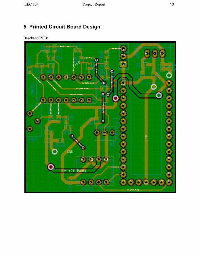
5. Printed Circuit Board Design Baseband PCB:

EEC 134 Project Report 11
RF PCB:

EEC 134 Project Report 12
6.Testing the System
When testing the RF signals, it is very difficult to isolate the cause of an error within a system. Under directions from the professor, we stripped a piece of cable and use the metallic core within to poke around the components. After some initial testing, the transmitted signal was read at 10.72 dBm, instead of the expected 12 dBm. In total, there is a loss of almost 23 dB. The signal is almost 200 times smaller than expected, thus it is not sufficiently powerful enough to transmit a recognizable signal. Below is a picture of the board we tested:
The next step in the testing process is to find the cause of this loss. To do this, we tested all components individually to see which component was not drawing power. If one of the components was drawing insufficient or no power, we could definitively say that is one of the causes. We cannot, however, claim that it is the only cause. For the case of the transmitted power, we had to test the VCO and the first amplifier. To measure the power, we read the voltage and current that was being drawn from the power supply using a bench multimeter. For the VCO, it was drawing 20mA at 5V, and the LNA was drawing 12mA at 3V. That is 100mW and 99mW, respectively. The expected value for the VCO is 33mA (max) at 5V (165mW. This was well within the expected range. However, the LNA max is at 25mA at 3V, which is 75mW. This is too small for amplifying the signal, thus we conclude that this is the source of our problem.

EEC 134 Project Report 13
After carefully consider all the components on the PCB board, we came to the conclusion that it is the LNA which caused the problems at hand. We decided to change all the LNAs on our PCB boards for new ones. At first this seems to work, for our output power goes back to 12 dBm. Here is the indoor results:
Unfortunately, one week before the competition, overheat from the VCOs and LNAs rendered the PCB board useless. Two team members recall strange smells during the testing. Here is the results after the incidents:

EEC 134 Project Report 14
Thus, we were forced to change back to our lab 6 system to participate in the competition. Here is a picture of the lab 6 system:
7. Results of the Competition
Following the instruction from TA Hao Wang, we conducted three testing experiments to measure the accuracy and the distance of our system. The results are as followed:

EEC 134 Project Report 15
● First experiment:
Real length is 52 m, measured to be 53 m. Error is 1.9% difference.

EEC 134 Project Report 16
● Second experiment:
Real length is 73 m, measured to be 72 m. Error is 1.36%.

EEC 134 Project Report 17
● Third experiment:
Real length is 91.4 m, measured to be 90 m. Error is 1.5%. The power of our entire system is 1.13 W ((8*0.06)+(5*0.13)) and the weight is 300 g. Overall, our system is within permitted limit.
8. Possibility for Future Extension
If there is possibility of future extension, we would wish to finish soldering a second RF board and test it out with the component. The second board has many improvements over the first board, such as better footprints and better overall layout. Furthermore, it is also made by a different producer, which could makes a difference in performance.
If we’re given a chance to do over, we would make changes to three aspects of the system. First of all, we would prefer to buy all components from the same producers, preferably Mini Circuits. In this manner, the components are much more compatible with each other and their footprints are easier to access. The reason for Mini Circuits is that the professor and the TA are knowledgeable about their components and give great advices on implementing them. The second aspect is accuracy level. As the above section shows, we eyeball all of our results on the
EEC 134 Project Report 18
graph and thus our accuracy is not great. If we have time, more attention should be paid to create an interface in Matlab so that an accurate reading of the distance is displayed immediately after the code stops. Last but not least, we wish to change the physical casing of the system. We didn’t concentrate on this as much as everything else and end up using a cardboard to hold the system, supported by screws and duct taped. This is not ideal however, and during the competition we were impressed by the attention some groups put into the casing. In hindsight, we would like house our components in a plastic box. The two can antennas will be placed on the sides, fasted to the box by strings or adhesive.
9. Suggestions for the Class ∙ It may be very helpful to have some tutorial sessions on PCB design. Many people had not designed a PCB before and learning to use PCB CAD software could be difficult for some. ∙ We also think it may be good to encourage students from other electrical engineering fields other than RF to take this senior design project class. This would allow for more diverse teams of students with different specialties. For example, a team with students with a lot of knowledge in digital signal processing and coding may be able to make a more innovative code, instead of just browsing the internet for a code that just does the bare minimum for the project.
10. Conclusion
We have found that EEC 134 was a great learning experience. The first quarter of the class was very helpful in teaching us what we need to know for designing the radar, like the general structure of a radar circuit and the components used to accomplish that. For some of us, it was the first time we were introduced to working with components such as voltage controlled oscillators (VCO) and mixers. It was also the first time for all of us did PCB design and it took us a long time to complete our PCB designs since we had to first familiarize ourselves with the software, find out how to do certain functions, and then actually lay down the design. The tasks completed in the first quarter really helped us in accomplishing the task given in the second quarter, which was to build an improved radar design. The task given in the second quarter was difficult to negotiate with at first, because we were unable to get the sixth lab from first quarter to work and also because the responsibility of choosing how to design a, not only functional, but also improved radar fell onto us. We had to find components that would at least match the firstquarter components in performance, are less bulky, and are easily obtainable for a decent price. We had to familiarize ourselves with the performance figures of the components to be able to compare them to each other so that we could get the best performance for the best price. At first we wanted to design a patch array

EEC 134 Project Report 19
antenna because it would have been much less bulky than the coffee can antennas, but we scrapped that plan and used the coffee cans because fabricating the patch array antenna would put us over budget. We were able to get a signal with our chosen components (LNAs, VCO, mixer, etc.) for a short time, but in the end too many of our amplifiers burned out before we could do a field test and we had to resort to using the firstquarter components for our RF circuit. In the end we able to get our radar to detect object up to 90 meters away. Our team was able utilize the skills we learned from our studies in UC Davis as well as learn many other aspects of RF design from this course. These courses gave us good experience in working as a team, teaching us how to solve problems, delegate tasks, and communicate in order to reach a goal. The skills and experience from this class is most beneficial to our growth as electrical engineers.