review’...
TRANSCRIPT

9/30/12
1
CS 61C: Great Ideas in Computer Architecture
Cache Performance
Instructors:
Krste Asanovic, Randy H. Katz
hEp://inst.eecs.Berkeley.edu/~cs61c/fa12
1 Fall 2012 -‐-‐ Lecture #15 9/30/12
New-‐School Machine Structures (It’s a bit more complicated!)
• Parallel Requests Assigned to computer e.g., Search “Katz”
• Parallel Threads Assigned to core e.g., Lookup, Ads
• Parallel Instruc^ons >1 instruc^on @ one ^me e.g., 5 pipelined instruc^ons
• Parallel Data >1 data item @ one ^me e.g., Add of 4 pairs of words
• Hardware descrip^ons All gates @ one ^me
• Programming Languages 9/30/12 Fall 2012 -‐-‐ Lecture #15 2
Smart Phone
Warehouse Scale
Computer
So.ware Hardware
Harness Parallelism & Achieve High Performance
Logic Gates
Core Core …
Memory (Cache)
Input/Output
Computer
Cache Memory
Core
Instruc^on Unit(s) Func^onal Unit(s)
A3+B3 A2+B2 A1+B1 A0+B0
Today’s Lecture
Review • Memory hierarchy exploits temporal and spa^al locality in instruc^on and data memory references from applica^ons
• Almost as fast as small, expensive memory, while having capacity of large, cheap memory.
• Cache is hardware-‐managed, programmer-‐invisible structure to hold copies of recently-‐used memory loca^ons – Cache hits serviced quickly – Cache misses need to go to memory, SLOW!
9/30/12 Fall 2012 -‐-‐ Lecture #15 3
• One word blocks, cache size = 1K words (or 4KB) Review: Direct-‐Mapped Cache
20 Tag 10 Index
Data Index Tag Valid 0 1 2 . . .
1021 1022 1023
31 30 . . . 13 12 11 . . . 2 1 0 Block offset
What if we used high bits of address as set index?
20
Data
32
Hit
9/30/12 4 Fall 2012 -‐-‐ Lecture #15
Student RouleEe
Valid bit ensures
something useful in cache for this index
Compare Tag with
upper part of Address to see if a Hit
Read data from cache instead
of memory if a Hit
Comparator
Address from CPU
Handling Stores with Write-‐Through
• Store instruc^ons write to memory, changing values
• Need to make sure cache and memory have same values on writes: 2 policies
1) Write-‐Through Policy: write cache and write through the cache to memory – Every write eventually gets to memory – Too slow, so include Write Buffer to allow processor to con^nue once data in Buffer
– Buffer updates memory in parallel to processor
9/30/12 Fall 2012 -‐-‐ Lecture #15 5
Write-‐Through Cache
• Write both values in cache and in memory
• Write buffer stops CPU from stalling if memory cannot keep up
• Write buffer may have mul^ple entries to absorb bursts of writes
• What if store misses in cache?
9/30/12 Fall 2012 -‐-‐ Lecture #15 6
Processor
32-‐bit Address
32-‐bit Data
Cache
32-‐bit Address
32-‐bit Data
Memory
1022 99
252
7
20
12
131 2041 Addr Data
Write Buffer

9/30/12
2
Handling Stores with Write-‐Back
2) Write-‐Back Policy: write only to cache and then write cache block back to memory when evict block from cache – Writes collected in cache, only single write to memory per block
– Include bit to see if wrote to block or not, and then only write back if bit is set • Called “Dirty” bit (wri^ng makes it “dirty”)
9/30/12 Fall 2012 -‐-‐ Lecture #15 7
Write-‐Back Cache
• Store/cache hit, write data in cache only & set dirty bit – Memory has stale value
• Store/cache miss, read data from memory, then update and set dirty bit – “Write-‐allocate” policy
• Load/cache hit, use value from cache
• On any miss, write back evicted block, only if dirty. Update cache with new block and clear dirty bit. 9/30/12 Fall 2012 -‐-‐ Lecture #15 8
Processor
32-‐bit Address
32-‐bit Data
Cache
32-‐bit Address
32-‐bit Data
Memory
1022 99
252
7
20
12
131 2041
D D D D
Dirty Bits
Write-‐Through vs. Write-‐Back
• Write-‐Through: – Simpler control logic – More predictable ^ming simplifies processor control logic
– Easier to make reliable, since memory always has copy of data
• Write-‐Back – More complex control logic
– More variable ^ming (0,1,2 memory accesses per cache access)
– Usually reduces write traffic
– Harder to make reliable, some^mes cache has only copy of data
9/30/12 Fall 2012 -‐-‐ Lecture #15 9
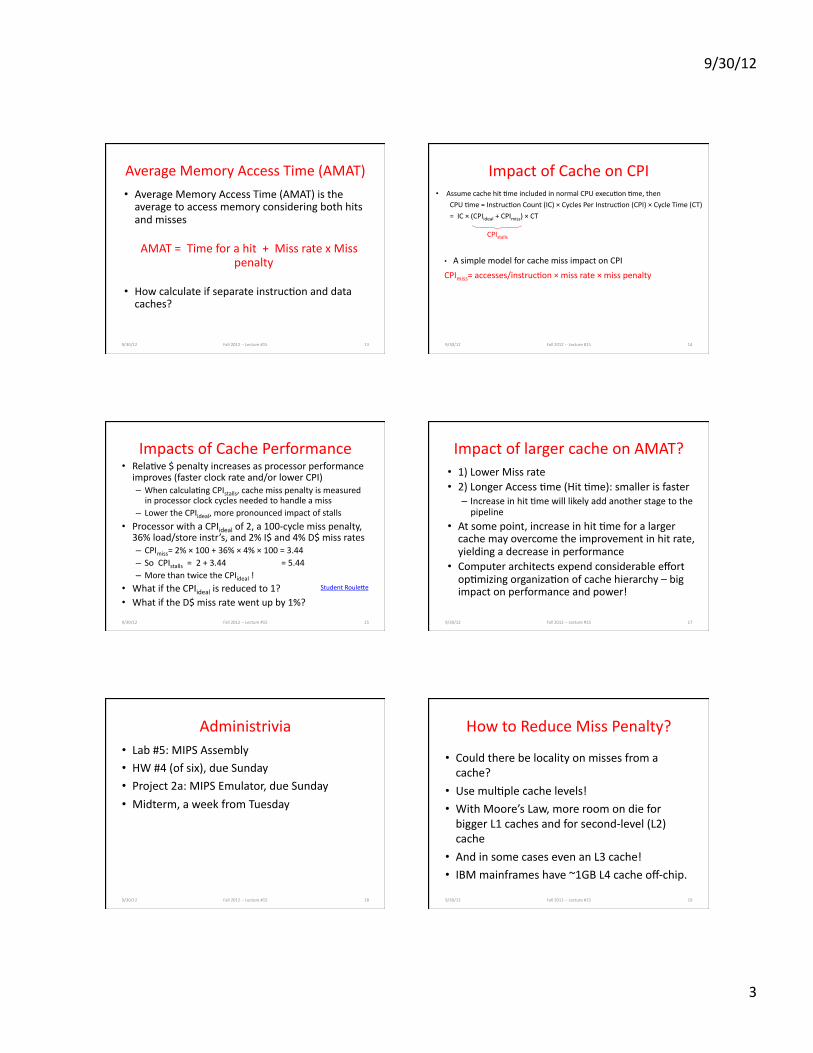
Average Memory Access Time (AMAT)
• Average Memory Access Time (AMAT) is the average to access memory considering both hits and misses in the cache
AMAT = Time for a hit + Miss rate x Miss penalty
9/30/12 10 Fall 2012 -‐-‐ Lecture #15
400 psec
600 psec!
≤200 psec ☐
☐
☐
☐
11
Average Memory Access Time (AMAT) is the average to access memory considering both hits and misses
AMAT = Time for a hit + Miss rate x Miss penalty
Given a 200 psec clock, a miss penalty of 50 clock cycles, a miss rate of 0.02 misses per instruc^on and a cache hit ^me of 1 clock cycle, what is AMAT?
Average Memory Access Time (AMAT) • Average Memory Access Time (AMAT) is the average to access memory considering both hits and misses
AMAT = Time for a hit + Miss rate x Miss penalty • What is the AMAT for a processor with a 200 psec clock, a miss penalty of 50 clock cycles, a miss rate of 0.02 misses per instruc^on and a cache access ^me of 1 clock cycle?
9/30/12 12 Fall 2012 -‐-‐ Lecture #15
1 + 0.02 x 50 = 2 clock cycles Or 2 x 200 = 400 psecs
9/30/12
3
Average Memory Access Time (AMAT)
• Average Memory Access Time (AMAT) is the average to access memory considering both hits and misses
AMAT = Time for a hit + Miss rate x Miss penalty
• How calculate if separate instruc^on and data caches?
9/30/12 13 Fall 2012 -‐-‐ Lecture #15
Impact of Cache on CPI • Assume cache hit ^me included in normal CPU execu^on ^me, then
CPU ^me = Instruc^on Count (IC) × Cycles Per Instruc^on (CPI) × Cycle Time (CT)
= IC × (CPIideal + CPImiss) × CT
9/30/12 Fall 2012 -‐-‐ Lecture #15 14
CPIstalls
• A simple model for cache miss impact on CPI
CPImiss= accesses/instruc^on × miss rate × miss penalty
Impacts of Cache Performance • Rela^ve $ penalty increases as processor performance improves (faster clock rate and/or lower CPI) – When calcula^ng CPIstalls, cache miss penalty is measured in processor clock cycles needed to handle a miss
– Lower the CPIideal, more pronounced impact of stalls
• Processor with a CPIideal of 2, a 100-‐cycle miss penalty, 36% load/store instr’s, and 2% I$ and 4% D$ miss rates – CPImiss= 2% × 100 + 36% × 4% × 100 = 3.44 – So CPIstalls = 2 + 3.44 = 5.44 – More than twice the CPIideal !
• What if the CPIideal is reduced to 1? • What if the D$ miss rate went up by 1%?
9/30/12 Fall 2012 -‐-‐ Lecture #15 15
Student RouleEe
Impact of larger cache on AMAT? • 1) Lower Miss rate • 2) Longer Access ^me (Hit ^me): smaller is faster – Increase in hit ^me will likely add another stage to the pipeline
• At some point, increase in hit ^me for a larger cache may overcome the improvement in hit rate, yielding a decrease in performance
• Computer architects expend considerable effort op^mizing organiza^on of cache hierarchy – big impact on performance and power!
9/30/12 17 Fall 2012 -‐-‐ Lecture #15
Administrivia • Lab #5: MIPS Assembly • HW #4 (of six), due Sunday
• Project 2a: MIPS Emulator, due Sunday
• Midterm, a week from Tuesday
9/30/12 Fall 2012 -‐-‐ Lecture #15 18
How to Reduce Miss Penalty?
• Could there be locality on misses from a cache?
• Use mul^ple cache levels!
• With Moore’s Law, more room on die for bigger L1 caches and for second-‐level (L2)cache
• And in some cases even an L3 cache!
• IBM mainframes have ~1GB L4 cache off-‐chip.
9/30/12 Fall 2012 -‐-‐ Lecture #15 19

9/30/12
4
Mul^ple Cache Levels • E.g., CPIideal of 2, 100 cycle miss penalty (to main memory), 25 cycle miss penalty (to L2$), 36% load/stores, a 2% (4%) L1 I$ (D$) miss rate, add a 0.5% L2$ miss rate – CPIstalls = 2 + 0.02×25 + 0.36×0.04×25
+ 0.005×100 + 0.36×0.005×100 = 3.54 (vs. 5.44 with no L2$)
9/30/12 Fall 2012 -‐-‐ Lecture #15 20
Second Level Cache (SRAM)
Typical Memory Hierarchy
Control
Datapath
Secondary Memory (Disk
Or Flash)
On-‐Chip Components
RegFile
Main Memory (DRAM) D
ata Cache
Instr Cache
Speed (cycles): ½’s 1’s 10’s 100’s 1,000,000’s
Size (bytes): 100’s 10K’s M’s G’s T’s
9/30/12 21 Fall 2012 -‐-‐ Lecture #15
• Principle of locality + memory hierarchy presents programmer with ≈ as much memory as is available in the cheapest technology at the ≈ speed offered by the fastest technology
Cost/bit: highest lowest
Local vs. Global Miss Rates
• Local miss rate – the frac^on of references to one level of a cache that miss
• Local Miss rate L2$ = $L2 Misses / L1$ Misses
• Global miss rate – the frac^on of references that miss in all levels of a mul^level cache • L2$ local miss rate >> than the global miss rate • O{en as high as 50% local miss rate – s^ll useful?
9/30/12 Fall 2012 -‐-‐ Lecture #15 22
Time for L1 hit + L1 Miss rate x L2 Miss rate x Miss penalty Time for L1 hit + L1 Miss rate x (Time for L2 hit + L2 Miss rate x Miss Penalty)
Time for L2 hit + L2 Miss rate x L2 Miss penalty ☐
☐
☐
☐
23
For L1 cache
AMAT = Time for a hit + Miss rate x Miss penalty
What is AMAT for system with L1 and L2 cache (L2 miss rate is local miss rate)?
Local vs. Global Miss Rates
• Local miss rate – the frac^on of references to one level of a cache that miss
• Local Miss rate L2$ = $L2 Misses / L1$ Misses • Global miss rate – the frac^on of references that miss in all levels of a mul^level cache • L2$ local miss rate >> than the global miss rate
• Global Miss rate = L2$ Misses / Total Accesses = L2$ Misses / L1$ Misses x L1$ Misses / Total Accesses = Local Miss rate L2$ x Local Miss rate L1$
• AMAT = Time for a hit + Miss rate x Miss penalty • AMAT = Time for a L1$ hit + (local) Miss rateL1$ x
(Time for a L2$ hit + (local) Miss rate L2$ x L2$ Miss penalty) 9/30/12 Fall 2012 -‐-‐ Lecture #15 24
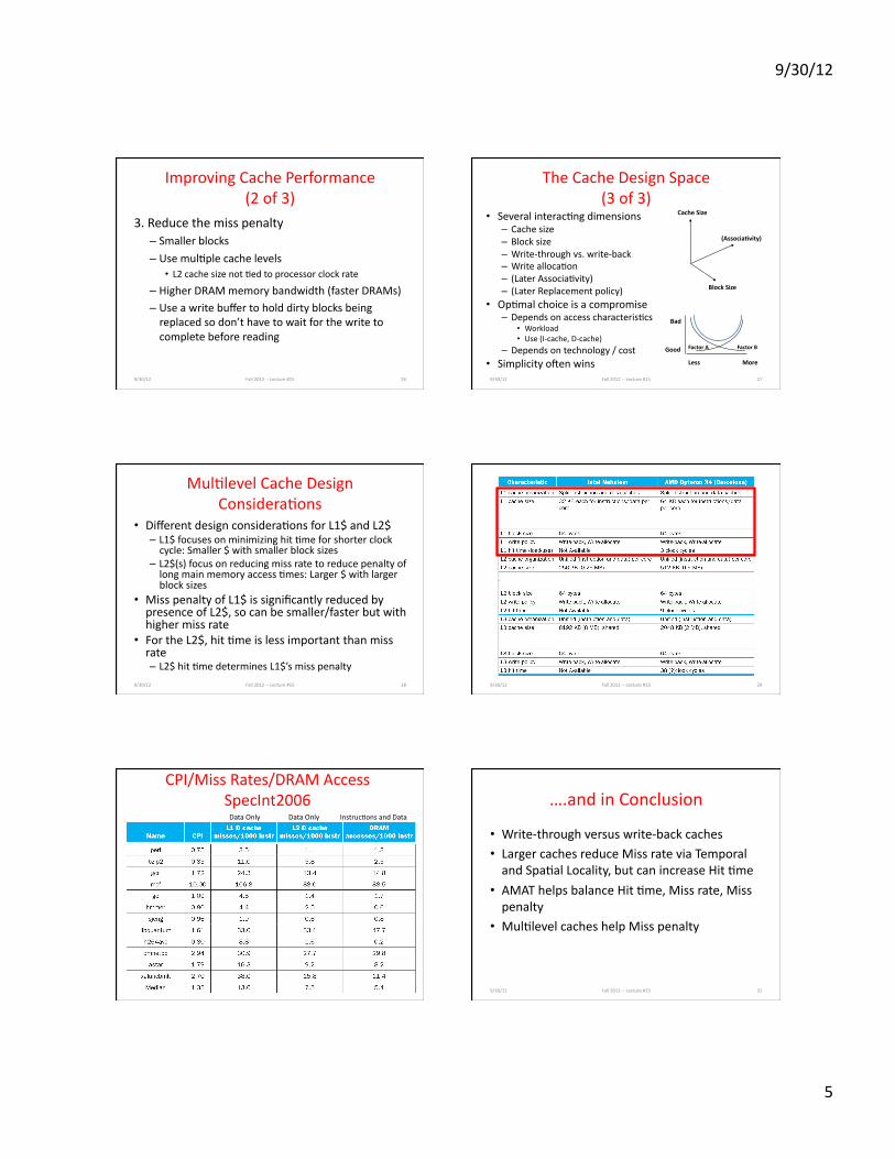
Improving Cache Performance (1 of 3)
AMAT = Hit Time + Miss rate x Miss penalty 1. Reduce the ^me to hit in the cache – Smaller cache
2. Reduce the miss rate – Bigger cache – Larger blocks (16 to 64 bytes typical) – (Later in semester: More flexible placement by increasing associa^vity)
9/30/12 Fall 2012 -‐-‐ Lecture #15 25
9/30/12
5
Improving Cache Performance (2 of 3)
3. Reduce the miss penalty – Smaller blocks
– Use mul^ple cache levels • L2 cache size not ^ed to processor clock rate
– Higher DRAM memory bandwidth (faster DRAMs) – Use a write buffer to hold dirty blocks being replaced so don’t have to wait for the write to complete before reading
9/30/12 Fall 2012 -‐-‐ Lecture #15 26
The Cache Design Space (3 of 3)
9/30/12 Fall 2012 -‐-‐ Lecture #15 27
• Several interac^ng dimensions – Cache size – Block size – Write-‐through vs. write-‐back – Write alloca^on – (Later Associa^vity) – (Later Replacement policy)
• Op^mal choice is a compromise – Depends on access characteris^cs
• Workload • Use (I-‐cache, D-‐cache)
– Depends on technology / cost • Simplicity o{en wins
(Associa;vity)
Cache Size
Block Size
Bad
Good
Less More
Factor A Factor B
Mul^level Cache Design Considera^ons
• Different design considera^ons for L1$ and L2$ – L1$ focuses on minimizing hit ^me for shorter clock cycle: Smaller $ with smaller block sizes
– L2$(s) focus on reducing miss rate to reduce penalty of long main memory access ^mes: Larger $ with larger block sizes
• Miss penalty of L1$ is significantly reduced by presence of L2$, so can be smaller/faster but with higher miss rate
• For the L2$, hit ^me is less important than miss rate – L2$ hit ^me determines L1$’s miss penalty
9/30/12 Fall 2012 -‐-‐ Lecture #15 28 9/30/12 Fall 2012 -‐-‐ Lecture #15 29
CPI/Miss Rates/DRAM Access SpecInt2006
9/30/12 Fall 2012 -‐-‐ Lecture #15 30
Instruc^ons and Data Data Only Data Only
….and in Conclusion
• Write-‐through versus write-‐back caches • Larger caches reduce Miss rate via Temporal and Spa^al Locality, but can increase Hit ^me
• AMAT helps balance Hit ^me, Miss rate, Miss penalty
• Mul^level caches help Miss penalty
9/30/12 31 Fall 2012 -‐-‐ Lecture #15