review - cornell university
TRANSCRIPT

Ultrawide-bandgap (UWBG) semicon-ductors, with bandgaps significantly wider than the 3.4 eV of GaN, represent an exciting and challenging new area of research in semiconductor materials, physics, devices and applications. This article surveys and presents an enumer-ated list of the materials, physics, device and associated application research op-portunities and challenges important for advancing the state of their science and technology.
J. Y. Tsao,* S. Chowdhury, M. A. Hollis, D. Jena, N. M. Johnson, K. A. Jones, R. J. Kaplar, S. Rajan, C. G. Van de Walle, E. Bellotti, C. L. Chua, R. Collazo, M. E. Coltrin, J. A. Cooper, K. R. Evans, S. Graham, T. A. Grotjohn, E. R. Heller, M. Higashiwaki, M. S. Islam, P. W. Juodawlkis, M. A. Khan, A. D. Koehler, J. H. Leach, U. K. Mishra, R. J. Nemanich, R. C. N. Pilawa-Podgurski, J. B. Shealy, Z. Sitar, M. J. Tadjer, A. F. Witulski, M. Wraback, J. A. Simmons ..... 1600501
Ultrawide-Bandgap Semiconductors: Research Opportunities and Challenges
REVIEW
Semiconductors
Semiconductors

Review
1600501 (1 of 49) © 2017 WILEY-VCH Verlag GmbH & Co. KGaA, Weinheim
www.advelectronicmat.de
Ultrawide-Bandgap Semiconductors: Research Opportunities and Challenges
J. Y. Tsao,* S. Chowdhury, M. A. Hollis, D. Jena, N. M. Johnson, K. A. Jones, R. J. Kaplar, S. Rajan, C. G. Van de Walle, E. Bellotti, C. L. Chua, R. Collazo, M. E. Coltrin, J. A. Cooper, K. R. Evans, S. Graham, T. A. Grotjohn, E. R. Heller, M. Higashiwaki, M. S. Islam, P. W. Juodawlkis, M. A. Khan, A. D. Koehler, J. H. Leach, U. K. Mishra, R. J. Nemanich, R. C. N. Pilawa-Podgurski, J. B. Shealy, Z. Sitar, M. J. Tadjer, A. F. Witulski, M. Wraback, and J. A. Simmons
DOI: 10.1002/aelm.201600501
Ultrawide-bandgap (UWBG) semiconductors, with bandgaps significantly wider than the 3.4 eV of GaN, represent an exciting and challenging new area of research in semiconductor materials, physics, devices, and applications. Because many figures-of-merit for device performance scale nonlinearly with bandgap, these semiconductors have long been known to have compelling potential advantages over their narrower-bandgap cousins in high-power and RF electronics, as well as in deep-UV optoelectronics, quantum information, and extreme-environment applications. Only recently, however, have the UWBG semiconductor materials, such as high Al-content AlGaN, diamond and Ga2O3, advanced in maturity to the point where realizing some of their tantalizing advantages is a relatively near-term possibility. In this article, the materials, physics, device and application research opportunities and challenges for advancing their state of the art are surveyed.
Semiconductors
Dr. J. Y. TsaoMaterial, Physical, and Chemical Sciences CenterSandia National LaboratoriesPO Box 5800, Albuquerque, NM 87185-1421, USAE-mail: [email protected]. S. ChowdhuryElectrical and Computer Engineering DepartmentUniversity of California Davis3133 Kemper Hall, Davis, CA 95616, USADr. M. A. HollisAdvanced Technology DivisionMIT Lincoln Laboratory244 Wood Street, Lexington, MA 02421-6426, USAProf. D. JenaElectrical and Computer Engineering and Materials Science and Engineering DepartmentsCornell University326 Bard Hall, Ithaca, NY 14853, USADr. N. M. Johnson, Dr. C. L. ChuaElectronic Materials and Devices LaboratoryPARC3333 Coyote Hill Road, Palo Alto, CA 94303, USADr. K. A. JonesSensors and Electron Devices DirectorateU.S. Army Research Laboratory2800 Powder Mill Road, Delphi, MD 20783, USADr. R. J. KaplarMaterial, Physical, and Chemical Sciences CenterSandia National LaboratoriesPO Box 5800, Albuquerque, NM 87185-1086, USA
Prof. S. RajanElectrical and Computer Engineering and Materials Science and Engineering DepartmentsOhio State University2015 Neil Avenue (Drees Labs 205), Columbus, OH 43210, USAProf. C. G. Van de WalleMaterials DepartmentUniversity of California Santa Barbara2510 Engineering II, Santa Barbara, CA 93106-5050, USAProf. E. BellottiElectrical and Computer Engineering DepartmentBoston University8 St. Mary’s Street Room 533, Boston, MA 02215, USAProf. R. CollazoMaterials Science and Engineering DepartmentNorth Carolina State University911 Partners Way (EBI 219), Raleigh, NC 27695, USADr. M. E. ColtrinPhysical, Chemical and Nano Sciences CenterSandia National LaboratoriesPO Box 5800, Albuquerque, NM 87185, USAProf. J. A. CooperElectrical and Computer Engineering DepartmentPurdue University1205 West State Street, West Lafayette, IN 47906, USADr. K. R. Evans, Dr. J. H. LeachKyma Technologies, Inc.8829 Midway West Rd, Raleigh, NC 27612, USAProf. S. GrahamMechanical Engineering DepartmentGeorgia Institute of Technology771 Ferst Drive, Atlanta, GA 30332, USA
Adv. Electron. Mater. 2017, 1600501

www.advancedsciencenews.com
© 2017 WILEY-VCH Verlag GmbH & Co. KGaA, Weinheim1600501 (2 of 49)
www.advelectronicmat.de
1. Introduction
Modern semiconductor technologies are only 70 years old, but have already transformed human society. At the heart of the technologies are the physical characteristics of the
Jeffrey Y. Tsao is currently a Distinguished Member of Technical Staff at Sandia National Laboratories. His Ph.D. is from Harvard University, under Professors Itamar Burak, Eli Yablonovitch and Nicolaas Bloembergen. From 1981 to 1991, he was research staff, first at MIT-Lincoln Laboratory then at Sandia, where he studied
laser microchemistry and the materials science of strained heterostructures. From 1991 to 2001, he was manager of compound semiconductor materials research at Sandia, then VP of R&D at E2O Communications. Since 2001, he has played a “national community organizer” role, spear-heading white papers which set national research strate-gies, including in solid-state lighting.
Mark A. Hollis received his Ph.D. from Cornell University in 1983 where he was in the renowned group of Prof. Lester Eastman. Dr. Hollis joined MIT Lincoln Laboratory where he co-supervised the fabrication of the first transis-tors ever to exceed an fmax of 200 GHz (265 GHz attained). Since then Dr. Hollis has made a number of contribu-
tions across the fields of electronic devices, optoelec-tronics, and biotechnology, and today he co-leads work in advanced materials and devices for future-generation systems.
Robert J. Kaplar received his B.S. degree in Physics from Case Western Reserve University, Cleveland, OH, and his M.S. and Ph.D. degrees in Electrical Engineering from Ohio State University, Columbus. He subsequently joined Sandia National Laboratories, Albuquerque, NM, as a post-doctoral researcher, and is
now a Principal Member of the Technical Staff at Sandia. His past work has included III-nitride optoelectronics and reliability physics, and he is currently focused on wide- and ultra-wide-bandgap III-nitride materials and devices for power applications.
Prof. T. A. GrotjohnElectrical and Computer Engineering DepartmentMichigan State University2120 Engineering Building, East Lansing, MI 48824, USADr. E. R. HellerMaterials and Manufacturing DirectorateAir Force Research Laboratory3005 Hobson Way, WPAFB, OH 45433, USADr. M. HigashiwakiTerahertz and Millimeter Wave ICT LaboratoryNational Institute of Information and Communications Technology4-2-1 Nukui-Kitamachi, Koganei, Tokyo 184-8795, JapanProf. M. S. IslamElectrical and Computer Engineering DepartmentUniversity of California at Davis3139 Kemper Hall, Davis, CA 95616, USADr. P. W. JuodawlkisQuantum Information and Integrated Nanosystems GroupMIT Lincoln Laboratory244 Wood Street, Lexington, MA 02421-6426, USAProf. M. A. KhanElectrical Engineering DepartmentUniversity of South Carolina301 Main Street (Swearingen 3A26), Columbia, SC 29208, USADr. A. D. Koehler, Dr. M. J. TadjerHigh Power Electronics BranchNaval Research Laboratory4555 Overlook Ave SW, Washington, DC 20375, USAProf. U. K. MishraElectrical and Computer Engineering DepartmentUniversity of California Santa Barbara2215C Engineering Science Building, Santa Barbara, CA 93106, USAProf. R. J. NemanichPhysics DepartmentArizona State UniversityPO Box 871504, Tempe, AZ 85287-1504, USAProf. R. C. N. Pilawa-PodgurskiElectrical and Computer EngineeringUniversity of Illinois Urbana-Champaign306 North Wright Street (4042 ECE), Urbana, Illinois 61801, USAProf. J. B. ShealyAkoustis Technologies9805-H Northcross Center Court, Huntersville, NC 28078, USAProf. Z. SitarMaterials Science and Engineering DepartmentNorth Carolina State University911 Partners Way (EBI 217), Raleigh, NC 27695, USAProf. A. F. WitulskiElectrical Engineering DepartmentVanderbilt University1025 16th Av. South, Ste. 200, Nashville, TN 37235-1553, USADr. M. WrabackSensors and Electron Devices DirectorateU.S. Army Research Laboratory2800 Powder Mill Road, Adelphi, MD 20783, USADr. J. A. SimmonsAdvanced Science and Technology DivisionSandia National LaboratoriesPO Box 5800, Albuquerque, NM 87185-1421, USA
The ORCID identification number(s) for the author(s) of this article can be found under https://doi.org/10.1002/aelm.201600501.
Adv. Electron. Mater. 2017, 1600501

www.advancedsciencenews.com
© 2017 WILEY-VCH Verlag GmbH & Co. KGaA, Weinheim1600501 (3 of 49)
www.advelectronicmat.de
semiconductor materials themselves: their fundamental elec-tronic and optical properties that enable electrons, holes and photons to interact and control each other in a wide variety of device architectures and operating environments.
In this introductory Section 1, we give a short review of the history of the materials on which various semiconductor tech-nologies are based, so as to place in a larger historical context the emerging ultrawide bandgap (UWBG) materials of interest to the larger article. Our review begins with the narrower bandgap materials Ge, Si and the III-As and III-P families and continues with the more recent wide bandgap materials InGaN/GaN and SiC. We then introduce the topic of this article, the emerging UWBG materials such as AlGaN/AlN, diamond and Ga2O3.
1.1. Ge, Si, and the “Conventional” III-V’s
For the first 40 years of semiconductor technology, through the late 1980s, the major semiconductor materials were Ge, Si and the “conventional” III-V’s.
The Ge- and Si-based technologies were spawned in 1947 by the demonstration of the first transistor.[1] The early devices were discrete and modest, but further development enabled the replacement of bulky, inefficient, and slow-turn-on vacuum tubes in applications that began with civilian radios and walkie-talkies but quickly expanded to police radios and later military communications satellites. Shortly thereafter, these devices were followed by integrated microelectronics, enabling the rise and spread of computer technology. By 2015, Si technology, dominated by Si complementary metal-oxide semiconductor (CMOS) architectures, had a direct economic impact measured by industry revenue of ≈US$330B per year,[2] and a far larger indirect impact on human society through its enabling of today’s information economy.
The “conventional” III-V’s refer to the narrower-bandgap subset of compound semiconductors composed of elements from columns III and V of the periodic table. An example is GaAs, in which half the atoms are gallium and half are arsenic, arranged in alternating positions within the atomic lattice. These III-V’s, dominated by the III-P’s and III-As’s, have been of interest since the 1950s, when fundamental measurements showed not only that their electron mobilities were superior to those of Si and Ge, but also that their bandgaps were direct (implying stronger electron/hole/photon interactions, useful for optoelectronic devices), wider (implying higher breakdown voltages useful for electronic devices), and might be amenable to compositional modulation (or “engineerable” as in so-called “bandgap engineering”).[3]
In electronics, the discovery[4] in the 1970s that the AlGaAs/GaAs heterojunction could give rise to a two-dimensional elec-tron gas (2DEG) was pivotal, enabling the first high-electron-mobility transistors (HEMTs) in GaAs[5] and thin pseudomor-phic strained InGaAs[6] channels. In the 1980s, these devices and their cousins, GaAs- and InGaAs-based heterojunction bipolar transistors (HBTs), quickly began setting records for unity-current-gain frequency (fT) and output power above 10 GHz. In 1989, recognizing these benefits, the U.S. Defense Advanced Research Projects Agency (DARPA) launched its
GaAs-based monolithic microwave integrated circuits (MIMIC) program.[7]
In optoelectronics, the invention[8] in the 1960s of the laser diode was just as pivotal. A long chain of progress led, among other devices, to the single-mode InP-based laser diodes that now power the broadband dense-wavelength-division-multi-plexed (DWDM) optical fiber networks, and which in turn are the backbone of the modern Internet.
1.2. Wide-Bandgap InGaN: Optoelectronics
Until the late-1980s, semiconductor technology was limited to Ge, Si, and the “conventional” III-V’s, all having relatively narrow bandgaps of less than ≈2.3 eV. The wider bandgap semiconductors had proven extremely challenging to develop, despite their obvious potential advantages—light emission in the visible for optoelectronics and higher breakdown voltages for electronics.
In the late 1980s and early 1990s, a series of pivotal materials breakthroughs were made by Isamu Akasaki, Hiroshi Amano, and Shuji Nakamura, for which they were awarded the 2014 Nobel Prize in Physics.[9,10] Their breakthroughs, built upon the efforts of many earlier researchers, were completely unex-pected: seemingly “magic” AlN and GaN buffer layers on sap-phire that dramatically reduced dislocation densities; methods to activate p-type Mg doping of GaN; and a remarkable resil-ience of InGaN quantum well luminescence against structural defects.
These breakthroughs unleashed, beginning in the late 1990s, huge worldwide research efforts into InGaN-based light-emit-ting-diode (LED) technologies. The research benefitted from government support, particularly for longer-term “precompeti-tive” challenges whose science and technological components were closely intertwined. Key milestones include the establish-ment of the “Next Generation Lighting Initiative”[11] and Solid-State Lighting program[12] by the U.S. Department of Energy’s (DOE’s) Office of Building Technologies, as well as the Energy Frontier Research Centers[13] established by the DOE’s Office of Science. The research also benefited from massive indus-trial support,[14] particularly for shorter-term challenges whose technological and use components were closely intertwined: for example, there is now a huge InGaN industrial ecosystem, anchored by a few very large InGaN LED chip companies such as Nichia, Samsung LED, Osram Opto Semiconductors, Lumileds, Seoul Semiconductor, Epistar and Cree.
At the time this is being written, in the late 2010s, InGaN has become the second most important semiconductor mate-rial after Si.[9] It is the basis for solid-state lighting (SSL), which is rapidly displacing conventional lighting and has the long-term potential for direct savings in world electricity consump-tion of 10% (equivalent to ≈US$100B per year)[14] as well as the emergence of new “smart and connected lighting” oppor-tunities for enhanced human productivity.[15] Most importantly, SSL is driving the development of an infrastructure that spans substrates, epitaxy, processing, devices, packaging, and applica-tions[16]—an infrastructure that can also be harnessed for other device architectures (electronics and optoelectronics) and mate-rials (other wide-bandgap semiconductors).
Adv. Electron. Mater. 2017, 1600501

www.advancedsciencenews.com
© 2017 WILEY-VCH Verlag GmbH & Co. KGaA, Weinheim1600501 (4 of 49)
www.advelectronicmat.de
1.3. Wide-Bandgap SiC and GaN: Electronics
While InGaN-based optoelectronics has been the main driver for the development of wide-bandgap (WBG) semiconductor materials, interest in electronics has also been high. Indeed, for electronics, some of the semiconductor material constraints that apply to optoelectronics are relaxed. Most importantly, bandgaps do not need to be direct, so SiC becomes a viable material; and light emission efficiency is not important, so GaN and AlGaN, not just InGaN, become workable materials. Of the two materials, SiC and GaN/AlGaN, SiC has the longer history.
Sustained investment in SiC electronics began in the late 1970s through the U.S. Department of Defense Office of Naval Research (program manager Max Yoder[17]), which catalyzed fundamental advances in SiC materials synthesis and quality, along with steady progress in a variety of device technologies. These included pn-junctions and Schottky diodes, metal–oxide-semiconductor and junction field-effect transistors (MOSFETs and JFETs) and bipolar junction transistors (BJTs). While Schottky diodes were the first devices to be commercialized in SiC (by Infineon in 2001), as of today all of the above device technologies have been commercialized in SiC.
Sometime thereafter, sustained investment in GaN elec-tronics began, also through the U.S. Department of Defense Office of Naval Research.[17] That investment was driven in part by improvements in SiC material quality leading to the suc-cessful demonstration of SiC as a substrate for high quality epi-taxial growth of GaN, and by the demonstration of high-quality GaN on sapphire substrates. Availability of epitaxial GaN tech-niques enabled the demonstration of the first AlGaN/GaN HEMT in 1993.[18] It quickly became recognized that GaN-based transistors had a significant power advantage over GaAs-based transistors, due to a much higher critical breakdown field and electron sheet density. Thus, beginning in the 2000s and accel-erating in the 2010s, U.S. government investment in GaN elec-tronics research deepened within the Department of Defense, especially by DARPA,[19] whose support enabled improved-relia-bility AlGaN/GaN HEMTs.[20] U.S. government investment also broadened to include the U.S. Department of Energy. Perhaps just as importantly, GaN-based electronics also began to take advantage of synergistic advances in InGaN optoelectronics and especially the huge InGaN manufacturing infrastructure driven by solid-state lighting.
All told, WBG SiC and GaN electronics are maturing rapidly, with a 2015 combined market size of ≈US$210M per year[21] and a significant ecosystem of small and large companies sup-plying devices for civilian and military applications. Recently, GaN RF/microwave HEMTs have been inserted into commer-cial cellular base stations. Significant future market growth is anticipated, particularly for power electronics applications in hybrid and electric vehicles, power supplies, and photovoltaic (PV) inverters.
1.4. Ultrawide-Bandgap Semiconductors: The Next Frontier
Even as the WBG semiconductor materials continue to mature, on the horizon are the ultrawide-bandgap (UWBG) semicon-ductor materials. These include AlGaN/AlN, diamond, Ga2O3
and cubic BN, and perhaps others not yet discovered. These materials have bandgaps significantly wider than the 3.4 eV of GaN—in the case of AlN as wide as ≈6.0 eV. Furthermore, because many of the figures-of-merit for device performance scale with increasing bandgap in a highly non-linear manner, these UWBG materials have the potential for far superior per-formance than conventional WBG materials have.
For example, in the simple case of a low-frequency unipolar vertical power switch, the widely used Baliga figure of merit (BFOM)[22] is defined as V2
BR/RON-SP. Here, VBR is the break-down voltage (the maximum voltage the switch can block when it is off), and RON-SP is the specific on-resistance (the inverse of the conductance per unit area when the switch is on). The higher the BFOM, the higher the voltage the device can block when off and/or the higher its conductivity per unit area when on. Because both breakdown voltage and conductivity depend on background doping and depletion width, which in turn depend on the critical electric field, EC, at which avalanche breakdown occurs, the BFOM can be expressed in terms of that critical field: ¼εµ C
3E , where ε is the electric permittivity and µ is the majority carrier mobility. The critical electric field, in turn, scales approximately as the square of the semicon-ductor bandgap, so the BFOM scales approximately as the sixth power of the semiconductor bandgap. In other words, moving from GaN to AlN gives an increase in bandgap by a factor of 1.8 ≈ 6.0 eV/3.4 eV, but a nonlinear increase in the BFOM of ≈ 34 ≈ (1.8)6.
This nonlinear increase is illustrated in Figure 1, in which lines of constant BFOM are drawn on a log-log specific on-resistance versus breakdown voltage plot. The lines drawn cor-respond to various conventional, WBG and UWBG semicon-ductors; the lines corresponding to the UWBG semiconductors trend towards the higher performance lower-right region of the plot. Note that for high-frequency high-power applications, the Johnson figure of merit (JFOM),[23] which can be written
Adv. Electron. Mater. 2017, 1600501
Figure 1. Contours of constant Baliga figure-of-merit (BFOM) for various conventional, WBG and UWBG semiconductors, drawn on a log-log spe-cific on-resistance versus breakdown voltage plot. This is the figure-of-merit of interest for low-frequency unipolar vertical power switches; the lower right region represents higher BFOM, hence higher performance.

www.advancedsciencenews.com
© 2017 WILEY-VCH Verlag GmbH & Co. KGaA, Weinheim1600501 (5 of 49)
www.advelectronicmat.de
as vsatEC/2π, where vsat is the saturated carrier velocity, is more appropriate than the Baliga figure of merit. One finds for this figure of merit as well that UWBG semiconductors offer significantly higher performance, as discussed later in Section 4.
Despite such tremendous potential for rev-olutionary device performance improvement, UWBG semiconductors are immature. While some of the UWBG semiconductors have been a topic of research for a decade or two, only recently have there been demonstrations of devices, and even then only in a small number of laboratories around the world. Thus, the UWBG semiconductors currently find themselves at a stage of development similar to that of the WBG semiconductors GaN and SiC in the 1980s—emerging mate-rials with many research challenges, but also with opportuni-ties for orders-of-magnitude improvement in performance both for existing applications and for application domains heretofore considered impossible to address.
In recognition of both the challenges and opportunities, a nascent community of UWBG researchers held two recent workshops. The First Technical Exchange on Ultrawide-bandgap Semiconductors was held October 19–20, 2015 in Albuquerque, NM. The Second Technical Exchange on Ultrawide-bandgap Semiconductors: Research Opportunities and Directions was held April 24–25, 2016 in Arlington, VA, under Air Force Office of Scientific Research (AFOSR) and National Science Founda-tion (NSF) sponsorship.
This article articulates the research challenges and oppor-tunities identified in that second workshop and fleshed out in subsequent months, with the hope that it will help serve in the short term as a research agenda for the community, and in the long term as a catalyzing agent for the realization of the poten-tial of UWBG semiconductor technology.
The remainder of the article is organized in the following manner. Section 2 reviews the UWBG materials landscape and its research opportunities and challenges, organized by mate-rial family: AlGaN/AlN, diamond, Ga2O3, and others. Section 3 reviews the UWBG physics landscape and its research oppor-tunities and challenges. Section 4 reviews the UWBG devices and applications landscape and its research opportunities and challenges. Throughout, we call out a set of especially impor-tant research opportunities and challenges, both scattered throughout the paper and compiled in summary in Section 5.
2. Materials
As mentioned in Section 1, it is only recently that control over UWBG materials synthesis and properties has advanced to the point where we can envision realizing some of their tantalizing advantages. A trio of materials has led the way—AlGaN/AlN, diamond, and Ga2O3—and these are the materials discussed in most detail in this Section 2. We emphasize, however, that the space of UWBG materials of potential future interest extends beyond these three, as will be touched on briefly in Section 2.4.
Here, to put just this trio of materials in context, Table 1 shows a few of their physical properties along with the states-of-the-art of three metrics important for device applications: the quality of their substrates as measured approximately by dislo-cations cm−2 and substrate diameter; their ability to be p-doped; and their ability to be n-doped. Some devices can meet specific applications even without good values for all three metrics: for example, a unipolar majority-carrier field-effect transistor (FET) may have reasonable performance without high substrate quality and with only one type of doping. But the widest range of devices are enabled by good values for all three; perhaps the most prototypical examples are the bipolar junction transistor (BJT) and the laser diode (LD), each of which requires both types of doping as well as high substrate quality to minimize parasitic recombination of minority carriers.
One can see that each of the three UWBG materials pres-ently has poor performance in their states-of-the-art in at least one of the three important metrics: AlN and Ga2O3 cannot (or can only poorly) be p-doped; and diamond has limited size or relatively poor quality substrates. One of our hopes with this article is to catalyze research that improves these metrics.
In the first three sub-sections of this Section 2, we discuss the three materials that are leading the way, and the research opportunities and challenges associated with advancing our control over their materials synthesis and properties. In the last two sub-sections of this Section 2, we discuss novel alternatives to these three materials, as well as a topic, doping, that cross-cuts all the UWBG materials.
2.1. AlGaN/AlN
The AlGaN alloys have exceptionally good fundamental phys-ical properties. From an electronics perspective, they have (1) direct bandgaps spanning a wide range (3.4 to ≈6.0 eV), (2) high breakdown fields (>10 MV cm−1 for AlN), (3) high elec-tron mobility (bulk mobilities up to 1000 cm2 V−1 s−1), (4) high saturation velocities (>107 cm s−1), and (5) relative ease at being doped n-type with Si, which has a relatively small donor ioniza-tion energy up to ≈80–85% Al content.[24–32] From an optoelec-tronics perspective, these alloys offer direct access to emission
Adv. Electron. Mater. 2017, 1600501
Table 1. Selected materials properties of WBG and UWBG semiconductors, including present-day states-of-the-art in key metrics of material quality and manipulability: substrate dislocation density, substrate diameter, and bulk p- and n-type doping levels. With respect to doping levels, by “good/moderate/poor/no” we mean relative to levels desirable for device technologies. More extensive sets of materials properties are given in Section 4.
Material WBG UWBG
GaN 4H-SiC AlGaN/AlN β-Ga2O3 Diamond
Bandgap (eV) 3.4 3.3 Up to 6.0 4.9 5.5
Thermal Conductivity (W m−1 K−1) 253 370 253–319 11–27 2290–3450
State-of-the-art substrate quality
(dislocations per cm2)≈104 ≈102 ≈104 ≈104 ≈105
State-of-the-art substrate diameter
(inches)
8 (on Si) 8 2 4 1
Demonstrated p-type dopability Good Good Poor No Good
Demonstrated n-type dopability Good Good Moderate Good Moderate

www.advancedsciencenews.com
© 2017 WILEY-VCH Verlag GmbH & Co. KGaA, Weinheim1600501 (6 of 49)
www.advelectronicmat.de
wavelengths shorter than about 365 nm, that is, into the UV-A, -B, and -C bands.
Moreover, AlGaN shares the same crystal structure as, and has overall material compatibility with, InGaN. Thus, it can readily take advantage of the huge global investment in the knowledge and manufacturing infrastructure associated with InGaN LEDs. Also, in common with InGaN, it is a ternary alloy, and thus can exploit the power of heterostructures and bandgap engineering just as have many other ternary alloys (AlGaAs, InGaAs, InGaP, etc.) in the III-V materials family. (Note that, though technically a ternary alloy, it is a so-called pseudo-binary alloy in that only the column III (Al,Ga) composition changes.)
However, the AlGaN alloys face three major challenges. The first challenge, control over doping, might be addressed in part by research approaches common to all the UWBG materials, and is discussed in Section 2.5. The second two challenges are addressed by research approaches more unique to AlGaN, and are discussed here. These are (1) the absence of readily available single-crystal substrates with the quality necessary for epitaxial growth; and (2) the immaturity of the scientific understanding required for control of heteroepitaxy on such substrates.
2.1.1. Single-Crystal Substrates
The starting point of almost all mature semiconductor technolo-gies is a high-quality substrate, lattice-matched or nearly lattice-matched to the active semiconductor material of interest that will be epitaxially grown upon it. InGaN optoelectronics tech-nologies are unique in that they have succeeded despite their common use of non-lattice-matched foreign substrates (such as sapphire and SiC) and the resulting high (≈108 cm−2) defect den-sities.[33,34] However, even these now-ubiquitous InGaN optoe-lectronics technologies improve markedly when they make use of low-defect-density single-crystal GaN substrates. We cannot discount the possibility that AlGaN technologies could be devel-oped with similarly good performance on non-lattice-matched foreign substrates, despite high defect densities. But it is over-whelmingly more likely that a high-quality lattice-matched or nearly-lattice-matched substrate will be needed.[35–38] Two pos-sible such substrates are being considered.
GaN substrates are the obvious possibility, as they are already being developed for InGaN optoelectronics and GaN power electronics technologies. However, high-quality epitaxial growth on GaN substrates is limited to lower-Al-content AlGaN suitable for WBG, not UWBG, applications (e.g., for lasers emitting at wavelengths longer than the middle of the UV-A band, about 365 nm). For higher Al-content AlGaN, the lattice mismatch between the epitaxial layers and the GaN substrate becomes increasingly large, and when strained epitaxial layers exceed their critical thickness, threading dislocations with some misfit component can be generated, which dramatically lowers device performance. Worse, AlGaN layers grown on GaN sub-strates are under tensile stress and are susceptible to forming extended cracks, which render the heterostructure useless. Indeed, this cracking is a common form of relaxation for the AlGaN alloys.[39]
AlN substrates are the more promising current possibility.[40,41] On such substrates, higher-Al-content AlGaN heterostructures
can be grown with relatively lower strain. And, even if the residual strain becomes significant, the strain is compres-sive rather than tensile and so does not tend to cause extended cracks. AlN substrates for epitaxy have made much progress, with multiple commercial suppliers in existence, including HexaTech and Crystal IS. Such substrates are expensive and limited in availability, however, and these practical factors are currently restricting the rate of progress in the development of high-performance UWBG electronic and optoelectronic devices.
Moreover, it is insufficient for the substrates just to have high crystalline quality and be large in diameter. They must also have low lattice “bow.” This is because heteroepitaxy is extremely sensitive to the atomic terrace and step structure of the growth surface (as discussed in the “Heteroepitaxy” sub-section below). Ideally, a growth surface has a low (one to two tenths of a degree) offcut away from a specific crystallographic direction. This offcut promotes a bilayer step-flow growth mode that enables uniform alloy and dopant composition of the epi-taxial layers.[42,43] If substrates have a significant lattice bow, the offcut of the growth surface will vary laterally, causing the bilayer step-flow growth mode to also vary laterally. In such a case, the alloy and dopant composition of the epitaxial layers will be non-uniform across the wafer.
To avoid this non-uniformity, the offcut deviation across a 5-cm wafer must be low, less than 0.1°.[42,43] From geometric considerations, the bow radius for a 5-cm wafer must be greater than 30 m; and for a 10-cm wafer must be greater than 60 m. These large bow radii are very difficult to achieve in practice. A key research opportunity/challenge, thus, is:
1. Materials: Large (>5 cm) diameter single-crystal AlN sub-strates with low (<104 cm−2) dislocation densities and negligi-ble bowing (radius of curvature >30 m).
A major obstacle to such AlN substrates is the extreme dif-ficulty of growing AlN boules from a melt, which is the tradi-tional approach to forming crystalline semiconductor boules free of dislocations, impurities, and bow. Except at very high pressures, AlN decomposes before it melts, so this method of substrate formation is not viable. Rather, alternative growth approaches are more actively being developed: for the III-nitrides, these are vapor-phase and solution-growth approaches. Because vertical epitaxy on a foreign substrate or on seed crystals leads to the bow mentioned above and illustrated in Figure 2, gradual crystal-size expansion of microscopic native seeds through iterative re-growth is preferred. However, since such expansion is slow, crystal size and production volumes remain low and wafer price is high. Note, though, that the approach to initial formation of the microscopic seeds does not need to be the same as that for lateral expansion to large areas or volumes. This raises the possibility of a mixed, or hybrid, approach. Indeed, very high quality homoepitaxial HVPE-grown GaN has recently been demonstrated using GaN seeds grown by the ammonothermal method.[44]
2.1.2. Heteroepitaxy
To realize the potential of AlGaN/AlN-based devices, it is not sufficient to have access to high quality, negligibly-bowed
Adv. Electron. Mater. 2017, 1600501

www.advancedsciencenews.com
© 2017 WILEY-VCH Verlag GmbH & Co. KGaA, Weinheim1600501 (7 of 49)
www.advelectronicmat.de
single-crystal AlN substrates. In addition, the growth of preci-sion “bandgap engineered”[3] heterostructures on these sub-strates is also necessary, and this requires precise control over the evolution of the atomic terrace and step structure of the sur-face during growth.
The degree of control differs considerably from the case of InGaN heteroepitaxial growth on sapphire and other non-native substrates, where the surface kinetic growth mecha-nism is simple spiral growth mediated by screw dislocations
that are present at a high density. Instead, for growth on low-dislocation-density native substrates, the surface kinetic growth mechanism is determined by an interplay (1) between the steps themselves (e.g., bilayer versus bunched steps), (2) between the adatoms and the steps (step-flow growth), and (3) between the adatoms themselves (nucleation on terraces). These three modes of interplay appear to be particularly difficult to con-trol for AlGaN/AlN heteroepitaxy. For example, Figure 3 shows a wide range of steady-state surface morphologies as a
Adv. Electron. Mater. 2017, 1600501
Figure 2. a) Schematic of a bowed substrate: initially grown by one-dimensional (vertical) epitaxy on either a lattice-mismatched or thermal-expansion-mismatched foreign substrate or seed; then released from that foreign substrate or seed by some chemical or physical process; upon which relaxation to its natural lattice constant takes place along with bowing. b) Even if that bowed substrate is polished flat, its lattice is still bowed, with the conse-quence that terrace widths decrease (step density increases) from the center to the edge of the wafer. c) An alternative approach might be growth on a native seed by iterative crystal expansion.
Figure 3. Atomic force microscopy (AFM) images of six distinct types of surface morphology observed for AlN homoepitaxial layers grown in the absence of dislocations. All were obtained under identical growth conditions but different out-of-plane offcuts. a) Growth on an on-c-axis AlN substrate with wide, atomically smooth terraces; due to large distances between steps, 2D nuclei formed on these surfaces and grew into epitaxial 3D islands. d) Growth on a surface with bilayer steps more densely spaced than in (a) but far apart enough that 2D nucleation on the terraces is still favorable. b) Growth on a surface with closely spaced bilayer steps (c/2) that yielded an RMS (root mean square) roughness of less than 50 pm. c,f) Step-bunched morphologies where the step heights are many times greater than the bilayer height; the difference between the straight and jagged step-bunch edges is due to the in-plane offcut direction. Finally, e) a meandering step morphology, which is a transitional stage between the bilayer and step-bunched morphologies. Reproduced with permission.[43] Copyright 2016, Elsevier.

www.advancedsciencenews.com
© 2017 WILEY-VCH Verlag GmbH & Co. KGaA, Weinheim1600501 (8 of 49)
www.advelectronicmat.de
function of terrace width (offcut angle) for the relatively simple homoepitaxial growth of AlN, all for the same nominal growth conditions.[42,43,45,46]
Moreover, since the surface kinetics of different adatom species of an alloy differ, the lateral compositional uniformity of ternary and quaternary alloys is directly related to the step structure. In particular, step-bunched surface morphology con-tains seemingly abrupt and undesirable lateral compositional gradients that are correlated with the differences in step density across such a surface. Therefore, in order to achieve a uniform composition in alloy films, controlling the surface morphology during alloy growth is critical.
To illustrate the challenge, Figure 4 shows results from the growth of AlGaN films on two substrates with different offcut angles: one has a uniform composition, while the other shows phase separation into two different compositions. Since AlGaN forms a complete range of solid solutions without a miscibility gap, the observed apparent phase separation is believed to be related to surface kinetics. This kind of compositional inhomo-geneity is highly detrimental to quantum well structures, as well as to carrier transport and breakdown fields that can be sustained across the structure.
Because the growth and morphology/composition co-evolution “phase space” is so crucial and so complicated, a key research opportunity/challenge is a predictive framework to guide the grower:
2. Materials: A predictive vapor-surface-film thermodynamic/kinetic framework for the atomic-scale co-evolution of mor-phology and composition during AlGaN heteroepitaxy.
Such a predictive framework would likely need to draw on a fundamental scientific understanding of the thermodynamics and kinetics of surfaces and adatoms. For example, what are the surface energies of the various crystallographic polar, non-polar, and semi-polar planes of interest? Accurately calcu-lating the surface energies from first principles is challenging, requiring a precise depiction of the surface reconstruction under particular growth conditions, including the effects of the polar nature of the wurtzite crystal structure,[47] and of the vapor supersaturation. Vapor supersaturation, in turn, depends on a wide range of parameters—temperature, of course, but also V/III ratio, diluent gas, and total pressure.[48] A related question is that of the surface kinetics of (and interactions between) various growth species on these surfaces, which are currently mostly unknown.
2.2. Diamond
Diamond has extremely advantageous properties that enable UWBG applications such as high-power and high-frequency electronics, radiation detectors, electron emitters for ultra-high voltage vacuum switches and traveling wave tube cathodes, and thermionic emitters for energy conver-sion. Some of diamond’s outstanding elec-tronic properties include: a breakdown field of >10 MV cm−1, high electron and hole mobilities >2000 cm2 V−1 s−1, and saturated drift velocities as high as 2.3 × 107 cm s−1 for electrons and 1.4 × 107 cm s−1 for holes (see Section 4). Diamond also has the highest known thermal conductivity of any material, of particular importance because in so many power electronics and optoelectronics appli-cations device operation is limited by heat removal. Some additional unique proper-ties include: excellent electron emissivity on hydrogen terminated surfaces,[49,50] surface-transfer doping enabled by these hydrogen-terminated surfaces,[51] room-temperature UV exciton emission, and optical defect centers due to the nitrogen-vacancy (N-V) and sil-icon-vacancy (Si-V) complexes. These defect centers have been proposed, as discussed in Section 4.5, as a physical qubit platform for emergent quantum information systems.[52]
Unlike AlGaN/AlN, which can borrow from a considerable body of InGaN/GaN materials knowledge and manufacturing
Adv. Electron. Mater. 2017, 1600501
Figure 4. AFM images of surfaces after AlGaN growth (during the same run) on a low (upper left) and high (upper right) offcut (from c-axis) AlN native substrate. The sample on the left shows bilayer steps, while the sample on the right is step-bunched. Although high-resolution X-ray diffraction (HRXRD) did not show any noticeable difference in the crystalline quality between the two films, low-temperature photoluminescence (PL) revealed for the bilayer growth mode a single emission peak (lower left), whereas the step-bunched film showed two distinct peaks corresponding to two different AlGaN compositions (lower right). Reproduced with permission.[42] Copyright 2016, Elsevier.

www.advancedsciencenews.com
© 2017 WILEY-VCH Verlag GmbH & Co. KGaA, Weinheim1600501 (9 of 49)
www.advelectronicmat.de
infrastructure, diamond is more unique and cannot borrow, for example, from the even larger body of knowledge and manu-facturing infrastructure of the material it is most similar to in crystal structure, Si. Nevertheless, two materials breakthroughs have stimulated much recent excitement over the diamond materials system.
The first breakthrough was the realization of single-crystal man-made substrates. Just as with AlGaN discussed above, the lack of large-area, low-defect-density, single-crystal diamond substrates has historically limited device concept demonstra-tion. In the past few years, however, a number of approaches have been developed that enable both relatively low defect density (<105 cm−2) substrates, as well as new synthesis strat-egies for larger substrates. Single-crystal diamond substrates with dimensions greater than 1 × 1 cm2 can now be prepared by high-growth-rate chemical vapor deposition (CVD) on (100) crystal faces, and are commercially available.[108] On the horizon are a number of potential approaches to larger-area substrates that could approach 50 mm in diameter: lateral tiling of smaller substrates created through smart-cut-like extraction from small-size, high-pressure, high-temperature (HPHT) grown boules; homoepitaxial growth using an iridium nucleation layer; repeated CVD overgrowth on existing small-size HPHT grown boules; and higher pressure and temperature HPHT boule growth.[104–107] Given that the typical CVD growth temperature is relatively low (≈850 °C) and the cost of high-purity elemental material is low, it may even be projected that substrate costs will be substantially reduced in the future. Even if larger sub-strates ultimately prove difficult to develop, “Minimal Fab” strategies for manufacturing on 12 mm diameter substrates are also being considered as viable options.[109–111]
The second breakthrough is efficient doping. Doped dia-mond layers are generally prepared by gas-phase doping during plasma-enhanced CVD growth on single-crystal diamond sub-strates. In the past decade, substantial progress has been made in p-type doping with boron, and just in the past few years n-type doping with phosphorus has been demonstrated at a number of laboratories. While dopant levels are deep (0.3 eV for B and 0.57 eV for P), impurity concentrations greater than 1020 cm−3 can be achieved, which provides low room-temperature resis-tivities through hopping conduction, and enables low-resistance electrical contacts. Moreover, as temperature increases, resis-tivity is reduced, making the performance of diamond devices potentially better at high operating temperatures, as well as potentially eliminating the thermal runaway often observed in other semiconductors at elevated temperature and/or high power operation.
With these two breakthroughs—the advent of substrates (albeit limited in diameter and availability, and at relatively high cost), and the demonstration of bipolar doping (albeit limited in achievable doping densities and resistivities)—there has been an explosion of diamond device studies. Unipolar Schottky diodes prepared with p-type diamond have demonstrated >5 kV breakdown voltage; bipolar pin diodes have demonstrated for-ward current densities greater than 500 A cm−2 and breakdown voltages greater than 1000 V; and vertical bipolar junction tran-sistors (BJTs) have been demonstrated on (100) and (111) sub-strates.[112] Both the bipolar pin diodes and BJT devices take advantage of the high electron and hole mobilities of diamond.
Additional excitement has been generated by new approaches to controlling and exploiting surfaces, as well as excitonic and defect-center properties.
The key surface property of diamond—the low electron affinity of its hydrogen-terminated surface (H termination)—is often associated with electron emission. Indeed, diamond sur-faces have demonstrated thermionic energy conversion, while pin diodes with H-terminated surfaces have shown efficient electron emission at room temperature and have been used in high voltage (≈10 kV) vacuum switches.[50] But the low electron affinity of diamond also enables surface doping on intrinsic diamond surfaces (similar to polarization doping in AlGaN/GaN). Early studies established that air adsorbates could lead to a two-dimensional hole gas (2DHG) with a sheet charge den-sity in the 1014 cm−2 range.[113] While these air-exposed surfaces are notably unstable, lateral metal–oxide-semiconductor field-effect-transistor (MOSFET) devices have now been fabricated with atomic-layer-deposited (ALD) dielectric layers, as illus-trated in Figure 5. These have exhibited sheet charge densities greater than 1013 cm−2, stability to ≈400 °C, and high-voltage and high-frequency operation.[51]
The key excitonic property of diamond is its high (80 meV) exciton binding energy. Because diamond, like Ge and Si, is an indirect-bandgap semiconductor, its light emission per se is unlikely to be very efficient; however, its large exciton binding energy has enabled room-temperature UV emission from pin diodes.[114]
The key defect-center property of diamond is its notable N-V and Si-V defect centers with their long spin-relaxation times. These defect centers show promise for use in quantum infor-mation and communication (single photon source) applications, and have now been incorporated in diamond devices in which applied voltages can change the charge state of the center.[115]
Diamond is now in an exciting “exploration” phase, in which the challenge is to build a toolkit of processes for controlling materials synthesis and properties. This would further build on and extend the substrate and doping breakthroughs mentioned above. A key research opportunity/challenge, thus, is:
3. Materials: A complete set of synthesis and processing tools for control of substrate diameter, defects, doping, carrier con-finement, contacts, and heterostructures in diamond-based materials.
Adv. Electron. Mater. 2017, 1600501
Figure 5. Right: Hydrogen termination of diamond lowers its ionization energy, driving electron transfer from the valence band at the surface into electronic states in adsorbates. Left: The resulting p-type surface con-ductivity, with holes confined to a subsurface layer of a few nanometers thickness, enables “surface-transfer-doped” field-effect transistors. Repro-duced with permission.[51] Copyright 2014, Cambridge University Press.

www.advancedsciencenews.com
© 2017 WILEY-VCH Verlag GmbH & Co. KGaA, Weinheim1600501 (10 of 49)
www.advelectronicmat.de
This toolkit would ideally address the full range of impor-tant materials challenges, including: (1) growth of larger-area diamond films on disparate substrates such as Si, or larger freestanding diamond plates; (2) reducing defect and impurity densities in substrates and epitaxial layers; (3) preparing stable dielectric interfaces that can sustain high-mobility 2D hole and electron channel conduction; (4) preparing low-resistance con-tacts to both p- and n-type diamond; and (5) formation of heter-ostructures (e.g., with c-BN) for high-mobility devices and III-V integration. As research progresses on all of these topics, new device concepts can be anticipated based on the outstanding, extreme, and unique properties of diamond materials.
2.3. β-Ga2O3
Of the UWBG materials currently of active interest, β-Ga2O3 is the newest and least mature. It is intriguing, however, because of (1) its fundamental materials properties, (2) the availability of affordable native substrates, and especially (3) the recent fabrication of a metal–semiconductor field-effect transistor (MESFET) with interesting properties.[62]
From an optoelectronics perspective, Ga2O3, like the other UWBG semiconductors, has a bandgap in the deep-ultraviolet (DUV) region. Thus, on the one hand, Ga2O3-based opto-electronic devices such as solar-blind DUV photodetectors are expected to be useful for a variety of applications (e.g., flame detectors). On the other hand, the complexity of optical pro-cesses in β-Ga2O3, as well as the inability to dope the material p-type, has so far prevented its application to bipolar devices such as light emitters.
From an electronics perspective, and in particular with respect to unipolar power device applications, Ga2O3 has some outstanding attributes. First, it has a bandgap wider than 4.5 eV, leading to a high breakdown electric field of ≈9 MV cm−1.[62,116–119] Second, it displays good controllability of n-type conduc-tion over a wide range of n ≈ 1015–1019 cm−3 through Si or Sn doping,[86,120,121] and an even more widely tunable resis-tivity spanning the range ≈ 10−3–1012 Ω·cm. Third, as seen in Figure 1, its estimated Baliga figure of merit (BFOM) is higher than those of WBG SiC and GaN (despite its relatively lower mobility), though not as high as those of UWBG AlN, diamond, and c-BN. This has provided strong motivation for the develop-ment of Ga2O3 power devices.
From the perspective of device functionality beyond elec-tronics or optoelectronics, other attractive applications for Ga2O3 include high-temperature signal processing, harsh-environment electronics, and wireless communication devices/circuits. With respect to harsh-environment operation, the inherent stability of Ga2O3 (as an oxide semiconductor) against oxidation and its wide bandgap are both important properties.
Perhaps the greatest advantage of Ga2O3 lies, as mentioned above, in the availability of affordable, high-quality, large native substrates, with the good material workability of Ga2O3 being an important feature for such economical mass substrate pro-duction. Today’s 2″ Ga2O3 substrates are priced similarly to 2″ GaN substrates (≈$2K per substrate in low volume), though cur-rently their delivered volume is much lower than that of GaN. Thus, should Ga2O3 devices begin to take off commercially,
the market price of Ga2O3 is expected to drop, perhaps even approaching that of sapphire at high volumes. The situation for Ga2O3 is thus very different from that for UWBG AlGaN or diamond, whose progress has been hampered by a lack of such substrates. Indeed, the availability of β-Ga2O3 substrates has also spawned efforts to use them as substrates for III-nitride epitaxial growth, due to the hexagonal symmetry and the rela-tively small lattice mismatch of less than 5% between GaN and Ga2O3. In fact, high-power InGaN-based LEDs have already been demonstrated on Ga2O3 substrates—taking advantage of these substrates’ high electrical conductivity and high optical transparency in the visible and UV ranges.[122]
At this point in time, Ga2O3 wafers can be fabricated in large volumes and at reasonable cost—with even lower costs possible should demand materialize. These wafers are fabricated from bulk single crystals synthesized by a variety of melt-growth techniques such as float-zone,[120,123] Czochralski,[124,125] ver-tical Bridgman,[126] and edge-defined film-fed growth (EFG) methods.[127–129]
To date, EFG has an advantage over the other melt-growth methods in producing such wafers. Figure 6 displays a photo-graph of a 4-inch-diameter single-crystal Ga2O3 wafer produced from an EFG-grown bulk crystal. The EFG Ga2O3 wafers have exhibited very high crystal quality, with a full-width at half-maximum of the X-ray diffraction rocking curve as narrow as 17 arcsec and a dislocation density on the order of ≈103–104 cm−2. Commercial substrates now have full-width at half-maxima of 150 arcsec,[130] as well as in-plane Sn doping concentrations and resistivities ±20%, acceptable for practical vertical devices. Note that the growth direction of EFG Ga2O3 growth is [010], with arbitrary orientations around the [010] likely possible by opti-mizing growth conditions. This growth direction naturally gives (–201) wafer surface orientations; other orientations are possible
Adv. Electron. Mater. 2017, 1600501
Figure 6. Photograph of transparent 4″-diameter single-crystal Ga2O3 wafer. Copyright Tamura Corporation via Masataka Higashiwaki, National Institute of Information and Communications Technology.
www.advancedsciencenews.com
© 2017 WILEY-VCH Verlag GmbH & Co. KGaA, Weinheim1600501 (11 of 49)
www.advelectronicmat.de
but with smaller diameters. Thus, other melt-growth methods may have advantages, depending on progress in device perfor-mance for these other wafer surface orientations.[131]
Two main drawbacks of Ga2O3 are often pointed out, how-ever, in discussions about the material’s power device potential.
First, in contrast to n-type material, there has been no report of successful p-type doping and thus of effective hole conduc-tion in Ga2O3. Self-trapping of holes, which prohibits effective p-type conductivity due to the resultant low mobility, has been predicted by first-principles calculations.[132]
Second, Ga2O3 has poor thermal conductivity and therefore poor heat-dissipation capability. This low thermal conductivity is perhaps the single most serious potential weakness of Ga2O3 for power devices. The experimental thermal conductivity values of Ga2O3 fall in the range of ≈10–27 W m−1 K−1 at room temperature, which is one or two orders of magnitude lower than those of other UWBG semiconductors.[91]
The first drawback, the absence of p-type doping, and the dif-ficulty of doping in general in the UWBG semiconductors, is discussed in Section 2.5. The second drawback, however, repre-sents a separate, but key, research opportunity/challenge:
4. Materials: Novel synthesis, processing, and architectural routes for circumventing the low thermal conductivity of Ga2O3.
Among these routes might be those based on thin-film sepa-ration methods or nanomembranes,[133] which enable exploita-tion of the favorable electronic and optoelectronic properties of Ga2O3 in conjunction with the thermal conductance properties of other materials such as poly-diamond or Cu. It might also be possible to grow Ga2O3 directly on high thermal conduc-tivity substrates such as SiC and diamond (single crystal and polycrystalline). Additional opportunities include polymorph control (since Ga2O3 can be stable in multiple phases), and the development of heterostructures, potentially with Al2O3 or In2O3.[134]
2.4. Other UWBG Materials
While AlGaN/AlN, diamond, and Ga2O3 are the UWBG mate-rials that have generated the most interest in recent years, all UWBG materials are relatively immature, and many others are worthy of exploration. For example, MgGa2O4,[135] Al2O3, II-IV-N materials such as ZnSiN2 and MgSiN2,[136] and possibly various 2D materials, are all of interest.
Of special interest, though, is BN. Of its sp2-bonded hexag-onal structures (hexagonal (h-BN),[137] rhombohedral (r-BN),[138] and turbostratic (t-BN)[139]), the wide bandgap of h-BN and the ability to synthesize single layers make it especially attractive for two-dimensional electronics or as an interlayer for heter-oepitaxy. In its sp3-bonded structure, BN can occur in multiple polymorphs, including zinc blende cubic (c-BN).[140,141]
In its wurtzite structure, wz-BN can potentially be alloyed with AlN or GaN to achieve wider band gaps. Though BN does not naturally occur in the wurtzite structure,[142] for low concen-trations of B, BGaN and BAlN alloys may maintain the wurtzite structure of GaN and AlN (although recent work has demon-strated the formation by MOCVD growth of a cubic phase of
BGaN for low (≈1%) B composition).[143] BN thus might serve as a natural extension of the nitride family of semiconductors that consists of InN, GaN, and AlN. Among the interesting applications of BAlN alloys are as hetero-barriers for BAlN/AlN majority-carrier structures, and as quantum barriers for AlN quantum wells (e.g., BAlN/AlN/BAlN), potentially enabling optoelectronics in the ultra-deep-UV range.
In its cubic structure,[144] c-BN is isoelectronic with diamond. Doping is obtained with Si and Be for n-type and p-type charac-ters, respectively. c-BN has a bandgap of 6.4 eV and is predicted to have a breakdown field greater than 15 MV cm−1. It has the second-highest thermal conductivity of all materials (theoreti-cally ≈2145 W m−1 K−1 for isotopically pure material)[94] and a small (1.4%) lattice mismatch with diamond that may enable, with the c-BN acting as an intermediary layer, integration of diamond with other III-V semiconductors.
Cubic BN faces challenges, however, particularly with regard to synthesis. Like carbon and as mentioned above, BN also possesses sp2-bonded phases. And, just like graphite versus diamond, the hexagonal phase of BN is more stable than the cubic phase and any growth process needs to avoid forming sp2-bonded regions.
c-BN films have been synthesized using several techniques including pulsed laser deposition,[145] ion-beam-assisted depo-sition,[146] e-beam evaporation,[147] various types of plasma-assisted chemical vapor deposition,[148,149] and physical vapor deposition.[150] In general, it is believed that the nucleation of c-BN requires energetic bombardment of the growing sur-face with charged or neutral ions, regardless of the synthesis approach. Degree of ion bombardment, strain, concentration of impurities (notably H), growth temperature, and issues related to adhesion to the substrate are all important factors that will determine the overall crystal structure and crystal quality in the c-BN films. A detailed discussion of the various approaches, along with extensive material characterization and analysis was reviewed by Samantaray and Singh.[151]
Because of these c-BN materials challenges, except for an early promising demonstration of a UV emitter,[152] progress toward realizing device technologies has been slow. A recent review of these efforts has been given by Zhang.[144]
A key research opportunity/challenge thus encompasses both the novel and much less explored UWBG materials, such as the various BN materials:
5. Materials: Exploration of novel UWBG materials (beyond AlN/AlGaN, diamond, and β-Ga2O3), including h-BN for 2D devices, wz-BN as an AlGaInN-alloying heterostructure-ena-bling material, and c-BN as a heterostructure with diamond and as a stand-alone material.
2.5. Doping
Since the birth of semiconductors, controlled shallow donor and acceptor doping has been the singular necessary step that transforms a semiconductor material from scientific curiosity to technological relevance. Though much progress has been made, breakthroughs similar to Mg acceptor p-type doping of GaN have not yet been achieved even for the most mature of the UWBG semiconductors: AlN, diamond, and Ga2O3. This is
Adv. Electron. Mater. 2017, 1600501

www.advancedsciencenews.com
© 2017 WILEY-VCH Verlag GmbH & Co. KGaA, Weinheim1600501 (12 of 49)
www.advelectronicmat.de
in part due to the presence of three obstacles not present in the traditional narrower gap semiconductors.
The first is the fact that most dopant ionization energies increase with bandgap. As ionization energy increases, the frac-tion of carriers that are thermodynamically “activated” from bound to free states decreases, making it difficult to achieve the UWBG free carrier concentrations at room temperature neces-sary for many devices.
Second, the wide bandgaps of UWBG materials can make them prone to self-trapping of carriers. In particular, the local-ized nature of valence-band states derived from elements of the first row of the periodic table (notably oxygen) can lead to for-mation of small hole polarons, in which a hole is self-trapped due to lattice distortions.[132] Even if suitable shallow acceptors could be identified, this tendency for carrier localization will suppress mobility.
Third, there is a prevalent tendency of dopants in UWBG semiconductors to undergo compensation via impurities, native defects, or defect complexes. This tendency is illustrated in Figure 7 for n-type doping of AlGaN by Si. As Si concen-tration increases, free carrier concentrations initially increase, but then reach a maximum and decrease—a signature of com-pensation, where vacancies and their complexes determine the net free-carrier density. Such compensation is universal to all UWBG semiconductors, not just AlGaN, since in general the formation energies of compensating defects decrease with increasing bandgap.
While the first and second obstacles are inextricably linked to fundamental materials properties, the third can benefit from materials engineering and merits closer inspection. Consider compensation by point defects. The equilibrium concentra-tion of point defects is determined by the defect free energy of formation, which in turn depends on the atomic and elec-tronic chemical potentials. Traditional synthesis approaches
typically control defect concentration by changing the atomic chemical potentials via control of growth conditions (species supersaturation) and temperature. The electronic chemical potential, or Fermi level, is controlled through the addition of impurity dopants with shallow defect states in the host mate-rial. Increasing the concentration of these impurities leads to a commensurate change in the Fermi level as extrinsic car-riers are added to the system. Although this holds true for all materials, the sizeable energy gap in UWBG materials leads to a significant change in the electronic chemical potential of compensating defects (ionized donors or acceptors for p- and n-type dopants, respectively). Unfortunately, charge neutrality can then be caused by having roughly equal concentrations of dopant impurities and compensating defects, effectively pin-ning the Fermi level far from the band edges and thwarting efforts to tailor conductivity.
Managing and achieving low compensation in UWBG mate-rials is thus challenging, though mandatory in order to supply devices with needed free carriers. Novel synthesis approaches coupled with advanced characterization may be necessary. For example, might new synthesis approaches be possible, such as maintaining non-equilibrium growth conditions, which would prevent the crystal from generating compensating defects? Moreover, because the synthesis phase space is so large, new theory for the relationship between synthesis and dopant properties must be developed to provide critical experimental guidance. Here, we call special attention to the development and exploitation of such theory in a research opportunity/challenge:
6. Materials: A first-principles theory of doping in UWBG semi-conductors in conjunction with new synthesis and doping ap-proaches (e.g., based on broken symmetries at surfaces and hetero-interfaces) that enables improved understanding and control of conventional doping methods.
Indeed, first-principles theory has contributed a framework for understanding and studying doping and compensation, and has already addressed a number of important problems.[153,154] Additional developments will be necessary, for instance to address non-equilibrium situations, to more rigorously calcu-late free energies, and to analyze self-trapping.
In addition to the overarching research opportunity/chal-lenge for a solution to doping that cuts across all the UWBG semiconductors, we now briefly mention here research oppor-tunities/challenges that are specific to particular UWBG semi-conductors and devices.
For AlGaN/AlN, which possesses spontaneous and piezo-electric polarization, new strategies that exploit broken crystal symmetries, such as polarization-induced doping, can poten-tially extend traditional chemical substitutional doping and offer significant opportunities for heterostructure engineering. Modulation doping may be useful for generating confined car-riers at heterointerfaces. However, the heterostructure composi-tions and band offsets over which such modulation doping can be effective will remain limited due to the deep-level defects in the wider-bandgap layers. Utilization of quasi-electric fields in graded bandgap layers could aid in ionizing dopants.
For diamond, which does not have the luxury of polarization doping, other strategies may be possible.
Adv. Electron. Mater. 2017, 1600501
Figure 7. Room-temperature carrier concentration as a function of sil-icon doping for AlGaN alloys with various Al percentages. As Si doping increases, free carrier concentrations initially increase, but then reach a maximum and decrease—a signature of compensation.

www.advancedsciencenews.com
© 2017 WILEY-VCH Verlag GmbH & Co. KGaA, Weinheim1600501 (13 of 49)
www.advelectronicmat.de
For example, a high surface conductivity can be achieved with surface transfer doping due to surface adsorbates.[51] This pro-cess, illustrated in Figure 5 and discussed in more detail in Sec-tion 2.2, can lead to a two-dimensional hole gas (2DHG) with hole densities above 1014 cm−2. The surface transfer doping is related to surface states, surface adsorbates and defects in the dielectric layer. The details of the interaction are an active area of research.
Or, for example, an additional approach to fabricating a pnp BJT in diamond using bulk doping might be to use B doping for the emitter and collector, and heavy B doping (≈1020 cm−3) for the emitter and collector Ohmic contacts. Such highly doped contact regions exhibit hopping conduction, which pro-vides low-resistance contacts without “classical” doping (i.e., holes excited to the valence band where they can freely con-duct). Doping the base with a P concentration of 1019 cm−3 is thought to be the optimum value since the donor ioniza-tion is light.[112] A low-contact-resistance Ohmic contact to the base can be made by regrowing a thin contact layer doped to >1020 cm−3 with P, although this increases the cost and com-plexity of the device.
For Ga2O3, there are a number of interesting doping ques-tions. Can stoichiometric Ga2O3 be routinely grown? Is the donor depth of the preferred n-type dopant (Sn) acceptably shallow, and can it routinely be inserted in the Sn+4 state as opposed to the Sn+2 state? Is its seemingly low measured mobility of 153 cm2 V−1 s−1[155] the maximum value, and if so, is that sufficient? Can 2DEGs be created using heterostructures with oxides based on other group-III metals like Al and In?
For cubic BN, among the doping challenges are the fol-lowing. Although not as deep as in diamond, at least one donor (Si) and two acceptor (Be and Mg) levels are >200 meV deep.[144] As mentioned in Section 2.4, control of chemical stoichiometry during synthesis can be difficult, and this is critical because boron vacancies act as acceptors and nitrogen vacancies act as donors. Also as mentioned in Section 2.4, BN has many dif-ferent phases, making it challenging to retain the cubic struc-ture during thermal removal of damage created by implanted dopants.
3. Physics
As discussed in Section 2, tantalizing progress is being made in UWBG materials synthesis and properties. Progress is now to the point where devices are being fabricated and tested, ena-bling the physics underlying device performance to be probed and explored. Because UWBG devices’ raison d’etre is to operate in new domains beyond those possible for conventional WBG or narrower-gap devices, our understanding of the solid-state physics underlying their operation is critical for advance-ment of the technology.
Perhaps the most important way in which this emerging UWBG device frontier depends on advances in our physics understanding will be in the very high electric fields at which the devices will operate. These high fields will drive physical phenomena much farther from equilibrium than in devices based on conventional semiconductor materials. Just as in other physical domains, probing regimes that have never before been
accessed can be anticipated to lead to the discovery of new phe-nomena. Fundamental concepts—in carrier dynamics and trans-port, doping and impurity scattering, electron–phonon coupling, photon emission and absorption, photoelectron emission, inter-face electronic band structure, and thermal conduction—may all undergo significant reexamination and refinement.
In addition, the interaction of electrons in UWBG semi-conductors with high-energy photons (exceeding ≈4 eV) and high-energy phonons (e.g., ≈0.16 eV in diamond) may lead to novel effects not seen in traditional semiconductors, including internal photoemission (since the photon energy is larger than the electron affinity) and robust superconductivity. Ultimately, we anticipate that this new solid-state physics understanding will enable a new generation of device designs with unprece-dented levels of performance.
In this Section 3, we articulate some of the research opportu-nities and challenges associated with exploration of these new physical domains, collectively captured with the following over-arching research opportunity/challenge:
7. Physics: Exploration of extreme high-field and non-equilib-rium physics regimes opened up by UWBG semiconduc-tors—regimes that will likely lead to re-evaluation of standard models for the fundamental properties of, and interactions between, the various carriers of energy (electrons, holes, pho-nons and photons).
In the following three subsections, we identify more spe-cific research challenges and opportunities regarding electronic transport, carrier confinement, and thermal transport.
3.1. Electronic Transport
Among the most important of electronic properties are the transport of electrons and holes in response to internal and externally applied electric fields. This area of physics is rich, governed by a wide range of carrier relaxation processes, all interacting in three different electric-field regimes (i) when electric fields are low and carrier velocities are linear in field, (ii) when electric fields are high and carrier velocities saturate, and (iii) when electric fields are so high that “breakdown” by avalanche multiplication occurs.
In this Section 3.1, we discuss what is known and not known about the physics of electronic transport in UWBG materials in these three different electric field regimes. The broad research opportunity concerning transport is:
8. Physics: A comprehensive understanding of the carrier and lattice dynamics underlying electron and hole transport—at low and high fields and in the breakdown regime—across the range of polar and non-polar UWBG semiconductors.
3.1.1. Low-Field Transport
With respect to the most basic transport property, low-field car-rier mobility, there are uncertainties with respect to all of the UWBG semiconductors.
In the III-N’s, transport in the least explored BN (both the hexagonal and cubic forms) materials remains largely
Adv. Electron. Mater. 2017, 1600501

www.advancedsciencenews.com
© 2017 WILEY-VCH Verlag GmbH & Co. KGaA, Weinheim1600501 (14 of 49)
www.advelectronicmat.de
unexplored. But uncertainties exist even for the relatively more mature III-N’s. Indeed, the III-N’s, taken to include the ternary, quaternary, or quinary (B,Al,Ga,In)N alloys, represent a rich yet untilled field for transport studies, both experimental and theoretical.
Experimentally, room-temperature electron mobilities in excess of ≈1000 cm2 V−1 s−1 can be achieved in very lightly doped bulk GaN, and hole mobilities of ≈24 cm2 V−1 s−1 can be attained in Mg-doped GaN samples.[29,65,74] The corresponding numbers are not yet clearly known in UWBG AlN, how-ever, primarily because control over doping levels has not yet reached the level of maturity it has in GaN. For degenerate elec-tron populations for which electron transport is not limited by impurity scattering (such as two-dimensional electron gases), the mobility in AlGaN is primarily limited by alloy and phonon scattering. In this case, the electron mobility drops significantly as the alloy composition is varied from GaN towards AlGaN, or AlN to AlGaN, and for mole fractions of Al or Ga larger than ≈10%, the electron mobility is dominated mainly by alloy scat-tering. As reported by Bajaj et al, electron mobilities can be factors of 2× or 3× lower than in GaN, based on conventional models.[156] Electron mobilities in doped AlGaN layers approach hundreds of cm2 V−1 s−1, and are slightly higher in polarization-induced 2DEGs.[54,66,157]
Theoretically, electron and hole transport properties are likely to require fundamentally new concepts and approaches, because of the highly mismatched electronic properties of the binary constituents. For example, consider the AlInN material system. The ≈6 eV energy bandgap of AlN is ≈10× the ≈0.6 eV bandgap of InN. Electronic states in narrower-gap AlGaAs or InGaAs ternaries can sometimes be treated as “averages” in the virtual crystal sense. They probably cannot be considered averages in that same sense for AlGaN, BGaN or the other UWBG III-N ternaries, however, because of the very large scat-tering potentials. Coupled with the randomly varying polariza-tion fields, low-field transport in UWBG ternaries is likely to be much more complicated than in narrower-gap ternaries.
Uncertainties in transport are even more pronounced in the relatively less mature β-Ga2O3 and diamond semiconductors.
In bulk β-Ga2O3, transport has recently begun to be explored—in particular, electron transport in material n-doped by Si and Sn, which form shallow donor states. Measured elec-tron mobilities are in the 100–200 cm2 V−1 s−1 range at room temperature, up to about 500 cm2 V−1 s−1 in the 100–200 K range for low-doped bulk material,[158,159] and up to even 5000 cm2 V−1 s−1 at 80 K in high-quality HVPE-grown epitaxial layers.[160] As illustrated in Figure 8, mobility in Ga2O3 appears to be limited by optical phonon scattering at high temperature and ionized impurity scattering at low temperature.[161] Hole transport has not yet been explored, since, as mentioned in Section 2.3, acceptor p-type doping is a severe challenge in this material system. It can be anticipated that the combination of a very heavy valence band effective mass and a strong Fröhlich interaction will lead to formation of polarons with very low conductivity.[162]
In β-Ga2O3-based alloys and heterostructures, transport is completely unexplored. 2D electron gases in heterostructures are yet to be created in this material system, though this is expected to happen as the material matures. Ternary alloys of
β–(AlxGa1−x)2O3/Ga2O3 have been reported;[164] however, in that study surface roughness arising from step bunching prevented carriers from forming a high mobility two-dimensional electron gas (2DEG). Nevertheless, first-principles calculations[134,165] have indicated that β–(Ga1−xInx)2O3 can be stable for low con-centrations of In, thus potentially enabling heterostructure devices using In-containing instead of Al-containing barrier layers.
In diamond, room-temperature electron and hole mobilities of ≈2000 cm2 V−1 s−1 are often reported, while electron mobili-ties above 4000 cm2 V−1 s−1 have been claimed from observa-tions of high-purity samples.[72] Moreover, cyclotron resonance measurements on ultra-pure substrates have shown low-tem-perature mobilities >106 cm2 V−1 s−1 and extrapolated room temperature values that exceed 5000 cm2 V−1 s−1 for holes and 7000 cm2 V−1 s−1 for electrons.[73] As highly crystalline diamond materials continue to become more available, low-field-trans-port measurements will perhaps probe regimes dominated by diamond’s exceptionally high threshold for phonon scattering, and explore the extremes of properties that follow from C residing at the top of the periodic table and possessing the most covalent of all bonds.
3.1.2. High-Field Transport
At high electric fields, electrons lose energy by optical phonon emission. This process governs the saturation of carrier veloci-ties in steady state (DC, or direct current) transport, and velocity overshoot in non-equilibrium situations. In addition, an under-standing of high-field ballistic transport in UWBG materials could spur their heterogeneous integration in applications for which a thin, wide bandgap material is required.
For polar UWBG semiconductors such as the nitrides, electron–phonon coupling is exceptionally strong, and drives a very high phonon-emission rate. This, combined with the
Adv. Electron. Mater. 2017, 1600501
Figure 8. Temperature dependence of the drift mobilities calculated for Ga2O3.[161,163] IO and NI indicate ionized and neutral impurity scattering; DP, NOP and PO indicate non-polar acoustic, non-polar optical and polar optical phonon scattering; the dotted line (NOP) represents the single NOP mobility. The bold solid line is the total drift mobility for all scat-tering mechanisms. Reproduced with permission.[161] Copyright 2016, IOP Publishing.

www.advancedsciencenews.com
© 2017 WILEY-VCH Verlag GmbH & Co. KGaA, Weinheim1600501 (15 of 49)
www.advelectronicmat.de
large mass difference between N and Ga, leads to a large gap in the phonon density of states between the acoustic and optical branches.[166–171] Such analysis typically implies an electron-density-dependent saturation velocity in the materials. These high-field transport properties have been investigated experi-mentally in WBG GaN, but not yet in UWBG AlGaN.[91,172] Saturation velocities of the order 107 cm s−1 are measured at electric fields above 0.1 MV cm−1 in GaN. High-field carrier saturation in the oxides and diamond are expected to follow similar trends since the effective mass is similar to that of GaN.
Improved understanding of transport physics would be of great benefit in the quest for high voltage (>20 kV) and RF ultrawide-bandgap devices, beginning with first-principles cal-culations and experimental verification of the high-field satu-ration velocities, impact ionization, and their dependences on carrier density and temperature. An example of an initial com-prehensive analysis of scattering mechanisms in Ga2O3, per-formed by Parisini and Fornari,[161] was discussed above and illustrated in Figure 8. A similar comprehensive analysis at high fields would be illuminating.
3.1.3. Breakdown
The principal promise of UWBG semiconductors lies in the high breakdown fields they can sustain. While critical break-down fields in GaN have been measured[59,60] to be in excess of ≈4 MV cm−1, those in AlN, BN, Ga2O3, and diamond are yet to be accurately determined. While the fields sustainable in these UWBG materials are expected to far exceed those in GaN and SiC, the physical mechanisms responsible for breakdown will likely involve new physics, for the following reason.
Because the bandgaps of most UWBG materials are larger than the electron affinity, breakdown mechanisms such as the onset of the avalanche process by impact ionization require carriers in the conduction band to have a kinetic energy larger than the electron affinity. This implies the carrier momentarily spends time in vacuum states before causing impact ionization. This sort of physics is new and unique to UWBG semiconduc-tors, and would have intriguing consequences for device design and operation.
In this area of avalanche breakdown, a key research opportu-nity/challenge is thus:
9. Physics: New theoretical descriptions and models of high-energy carrier transport and avalanche breakdown in UWBG materials, coupled with experimental verification.
3.2. Carrier Confinement
As with devices based on narrow-bandgap semiconductors, those based on UWBG semiconductors will benefit greatly from their ability to confine carriers (electrons and holes)—either for simple passivation or for engineering the active region (e.g., FET gate dielectrics).
For the highly desirable normally-off power devices discussed later in Section 4.2, gate insulators would enable carrier confinement and hence the normally-off MOSFET-like devices that are commonplace in narrow-gap Si, and that have
been demonstrated in WBG SiC and GaN.[173] Towards that end, materials such as Al2O3 (itself an UWBG semiconductor in its crystalline form), SiO2, and Si3N4 have been used in con-ventional AlGaN/GaN power HEMTs to limit gate leakage in normally-off, gate-recessed structures (in these structures the gate dielectric is deposited on the AlGaN barrier layer).[174] Also, Al2O3 deposited on AlGaN has been shown to affect HEMT properties such as 2DEG density and mobility.[175,176] More exotic dielectrics such as MgCaO, a crystalline material that can be lattice-matched to InAlN and AlGaN over a range of compo-sitions, have also shown promise.[177,178]
In general, the wider the bandgap of the semiconductor, the more difficult is the carrier confinement. For thin semicon-ductors where quantum confinement and bandgap widening occurs, this is extremely important. Indeed, the WBG and UWBG semiconductors have recently sprung a few surprises in the limit of extreme thinness: 2D GaN and quasi-2D Ga2O3 have been fabricated by sublimation or mechanical exfoliation, respectively,[133,179] potentially enabling significant increases in energy gap as fewer monolayers of material are isolated (e.g., 5.28 eV for 2D GaN). These ultrawide bandgaps, comparable even to the 5–6 eV of h-BN, will likely motivate research in advanced techniques for layer-by-layer epitaxial growth of both WBG and UWBG semiconductors.
Indeed, it is rather remarkable from a fundamental physics standpoint that these ultrathin (≈0.9 monolayers) GaN quantum wells and ultrasmall (≈0.56 nm) GaN quantum dots, by sheer quantum confinement between AlN barrier layers, can push bandgaps up to 5 eV or more.[180,181] This is even higher than what is claimed for a 2D version of GaN, and is enabled by the very large band offsets offered by UWBG semiconductor heterostructures, able to confine severely quantized states within the wells. This sort of engineering of quantized states also expands the scope of bandgap-engineered physics and devices, and offers unique opportunities in ultra-fast tunneling and inter-sub-band devices, possibly in the 1.55 µm regime of importance for free-space and optical-fiber communications.
Despite these tantalizing advances, challenges to carrier confinement abound. As the bandgap of the semiconductor increases, the number of suitable semiconductors or insula-tors with large enough band offsets available for carrier con-finement decreases. As illustrated in Figure 9, the UWBG semiconductors have conduction bands that trend towards the vacuum level. There are few dielectric layers with a predicted band alignment that will confine electrons in AlN, BN or dia-mond. In contrast, there are a number of dielectric layers that will confine holes, with Al2O3 and SiO2 having shown good results for diamond. New UWBG materials such as AlF3 could also be considered for gate dielectric or passivation applica-tions. The most fundamental obstacle is that any dielectric with a large bandgap will tend to have a low dielectric constant—and vice versa. This problem restricts the possibility of the high-k dielectrics desirable for realizing high-performance UWBG MOSFETs in the future, and is an extremely important research opportunity/challenge.
Note, however, that it is not sufficient for the band offsets of the confining semiconductor or insulator to be theoretically large enough to enable confinement. From a practical point of view, both the confining layer and the interface between the
Adv. Electron. Mater. 2017, 1600501

www.advancedsciencenews.com
© 2017 WILEY-VCH Verlag GmbH & Co. KGaA, Weinheim1600501 (16 of 49)
www.advelectronicmat.de
active semiconductor and the confining layer must be relatively defect free. The absence of defects would enable gate dielectrics to exhibit minimal hysteresis when subjected to IV sweeps of opposite polarity, and also to have good reliability (especially threshold voltage stability). The presence of defects, in contrast, leads to charge trapping either at the insulator–semiconductor interface or within the dielectric itself; thus, bulk and interface state density must be minimized. For example, SiC/SiO2 MOS-FETs have suffered from poor channel mobility and threshold voltage stability, due primarily to issues with defects at the SiC/SiO2 interface.[186]
Similar issues are expected for the UWBG semiconductors; indeed, the issues are expected to be more severe, both for epi-taxial and non-epitaxial insulators. For confinement by epitaxial insulators, trapping effects associated with gate insulators have been documented numerous times for power HEMTs based on the epitaxially “simplest” AlGaN/GaN interface, and are at pre-sent a significant area of study in the reliability physics commu-nity.[187] For confinement by non-epitaxial insulators, the prime example is the Si/SiO2 interface. However, SiO2 cannot be ther-mally grown with as high-quality an oxide on non-Si-containing materials as it can be on Si or SiC. This is a potentially rich area of materials science and device physics, as researchers search for the thus-far elusive semiconductor/insulator system that displays the astounding robustness of the Si/SiO2 interface. Note that Figure 9 includes Al2O3 in both crystalline and amor-phous forms, with the interesting possibility that Al2O3 could be both a dielectric (amorphous form) and an UWBG semicon-ductor (crystalline form).[188]
In general, surface states are likely present in all UWBG materials, and there have been studies that have explored their role in interface band structure and defect formation. For
dielectric–nitride interfaces, near-interface states are sometimes termed border traps, and appear to be influenced by polariza-tion fields.[189] Polarization fields, in turn, can potentially be manipulated, both to influence the interface and/or border states, and to enhance confinement.
In this area of carrier confinement, key research opportuni-ties/challenges are:
10. Physics: Exploration of the physics of carrier confinement under extreme conditions (e.g., ultrathin heterostructures whose confinement requires UWBG semiconductors).
11. Physics: High-k, ultrawide-bandgap dielectrics with low- interface-state-density interfaces to UWBG semiconductors.
3.3. Thermal Transport
The performance of many semiconductor devices is limited by heat removal. This is expected to be all the more critical for UWBG semiconductor devices, which will be driven “harder” (at higher current densities) than their narrower-gap cousins. Further, to fabricate devices with the desired electronic proper-ties, UWBG devices may make use of a number of materials and device building blocks: binary, ternary, and quaternary com-pounds; tailored doping; interfaces between dissimilar mate-rials; and UWBG materials that exhibit the highest thermal conductivity of all crystals (e.g. diamond, BN) as well as UWBG materials that exhibit among the lowest (e.g., Ga2O3). The result will be a complex set of internal impedances to heat conduction and removal, in some cases limiting device performance. As one simple example, Figure 10 shows how the creation of alloy semiconductors from the SiGe[190] and AlGaN[191] material sys-tems results in thermal conductivities far lower than those of their end-point materials—Si and Ge, or AlN and GaN, respec-tively—due to increased alloy scattering of phonons.
With these challenges comes opportunity, however. Are there architectures that can exploit this large range of properties as well as the wide variety of ways in which those properties can be
Adv. Electron. Mater. 2017, 1600501
Figure 9. Schematic of band alignment of WBG and UWBG semiconduc-tors (left side) and possible passivating dielectric materials (right side). The alignments are based on calculated charge neutrality levels or from experimental reports. The energy zero in the schematic is the charge neu-trality level. The numbers above each conduction band minimum (CBM) line represent the bandgap, and the numbers below each valence band maximum (VBM) line represent the position of the charge neutrality level relative to the VBM. References: (a) Monch;[182] (b) Fonseca, Liu and Robertson;[183] (c) König, Scholz, Zahn and Ebest;[184] and (d) Izumi, Hirai, Tsutsui and Sokolov.[163] Adapted with permission.[185] Copyright 2006, AIP Publishing.
Figure 10. Thermal conductivity of SiGe and AlGaN alloys as functions of Ge and Al content. The plot shows experimental data as well as predic-tions of the virtual crystal model (VCA) which shows the strong depend-ence on alloy composition.

www.advancedsciencenews.com
© 2017 WILEY-VCH Verlag GmbH & Co. KGaA, Weinheim1600501 (17 of 49)
www.advelectronicmat.de
integrated into a device? If so, can one manipulate thermal proper-ties to nearly the same level of precision as electrical properties, and ultimately tailor both in the device design and modeling process?
We are far from having in hand such methods for co-design of both thermal and electrical properties, however. At present, detailed models exist for electrical transport including full-band Monte Carlo down to continuum-scale hydrodynamic codes. However, most of these models treat thermal transport very simply, neglecting important interface and non-continuum effects, and even at a continuum level do not take into account the interplay between electrical and thermal responses at the relevant spatial and time scales.
Moreover, it will be necessary to develop a more sophisti-cated theoretical and experimental understanding of thermal transport in these materials and device architectures.
Our theoretical understanding of thermal transport in the UWBG semiconductors is relatively immature: the framework of the phonon gas model, which has been used to correlate thermal conductivity of semiconductor alloys, has not shown sufficient predictive capability to determine which UWBG materials will have large or small thermal conductivities. Recently, though, a molecular dynamics framework (the Green–Kubo modal analysis, or GKMA method) has shown a remarkable ability to predict the thermal conductivity of crystals and alloys.[192] A key research opportunity is thus to apply this and other atom-istic modeling approaches to better understand the phonon and vibrational-mode physics in UWBG materials and at their interfaces. One practical example is as follows: current efforts to use CVD diamond to remove heat from nitride devices appear to be limited by the quality of the interface between GaN and diamond.[193] Understanding such interfaces will become impor-tant as device designers begin to transfer and bond low-thermal-conductivity devices to higher-thermal-conductivity substrates.
Our experimental understanding of UWBG materials is also relatively immature. For example, while the thermal conductivity of Ga2O3 is known to be in the vicinity of 27 W m−1 K−1 at room temperature,[91] very little is known about doped materials and ternary systems made with Ga2O3. Moreover, because it will not always be feasible to fabricate special structures designed solely for the measurement of thermal properties, there is a need to develop thermal metrology approaches that can extract the spatial and temporal distribution of the thermal gradients in working UWBG devices. Indeed, over the past decade a number of tech-niques have been developed to measure the thermal response in GaN RF and power devices, improving the accuracy over that obtained using IR thermography.[194–199] The most prominent of these methods is Raman spectroscopy—a thermal metrology method that has been used to measure vertical temperature gra-dients inside UV-C LEDs and AlGaN/GaN HEMTs.[200] More recently, methods based on transient Raman spectroscopy and transient thermoreflectance have enabled measurements of the thermal response in AlGaN/GaN HEMTs with a time reso-lution <100 ns and temperature resolution less than several degrees.[201,202] Such techniques can yield real-time, in-situ data on specific heat, thermal conductivity, and thermal boundary resistance—all of which are parameters needed for accurate electro-thermal modeling of devices under transient operation.
Overall, these new space- and time-resolved thermal metrology methods are expected to yield critical information on
temperature rise and other thermal phenomena for both power and RF devices, and will help to refine electro-thermal models of UWBG devices with experimental data that is on the same time-scale and spatial resolution as the simulation techniques. Going forward, however, it will be important to better under-stand the accuracy and limits of these new techniques.
Thus, in this area of thermal transport, a key research oppor-tunity/challenge is:
12. Physics: New techniques for monitoring space- and time-var-ying temperature profiles, and for modeling and co-designing devices for combined electrical and thermal performance.
4. Devices and Applications
The ultimate goal of UWBG semiconductors is to enable devices that improve, even revolutionize, applications, including new applications that do not yet exist. The ability to handle large amounts of power is certainly one common theme for UWBG applications, but there are many other themes. In this Section 4, we review the landscape of known UWBG devices and applications, and articulate some of the key device-level research opportunities and challenges that might enable them. However, we emphasize that we survey only the known applications—with the understanding that the new technology capabilities represented by UWBG semiconductors will surely create applications that do not yet exist.
We organize this Section 4 in the following way. In Section 4.1, we provide a much more comprehensive version of the summary of materials properties in Table 1 at the begin-ning of Section 2. In Section 4.2, we review high-power elec-tronics technology, in which high voltages and/or high currents are switched. In Section 4.3, we review RF power/switching technologies, in which the intent is to transmit and receive RF power at high frequencies for long-distance communication or imaging. In Section 4.4, we review deep-UV optoelectronic technologies relevant to a variety of applications. In Section 4.5, we review quantum information applications. In Section 4.6, we review a particularly important cross-cutting feature of all UWBG technologies—their robustness and thus ability to operate in extreme environments, including high-radiation environments. Finally, in Section 4.7, we discuss device pro-cessing, modeling/calibration, and packaging.
4.1. Materials/Device Types and Properties
As an aid to navigating the UWBG materials and device landscape, in this Section 4.1 we summarize the results of a comprehensive survey and analysis of the room-temperature materials properties most relevant to electronic applications. Our intent is to provide the most current and accurate proper-ties available at the time of writing. It was necessitated in part by the fact that many material properties (even for GaN) were determined by measurements performed decades ago on mate-rial that was highly defective by today’s standards.
The results of the survey and analysis are summarized in Table 2 and discussed below. We consider first the materials/device
Adv. Electron. Mater. 2017, 1600501

www.advancedsciencenews.com
© 2017 WILEY-VCH Verlag GmbH & Co. KGaA, Weinheim1600501 (18 of 49)
www.advelectronicmat.de
Adv. Electron. Mater. 2017, 1600501
Tabl
e 2.
Mat
eria
l/de
vice
pro
pert
ies
for
elec
tron
ic a
pplic
atio
ns. C
olum
ns A
–H r
epre
sent
var
ious
WB
G a
nd U
WB
G s
emic
ondu
ctor
s, a
s w
ell a
s pa
rtic
ular
dev
ice
type
s of
spe
cial
inte
rest
. Row
s 1–
8 re
pres
ent
para
met
ers
that
cha
ract
eriz
e fu
ndam
enta
l phy
sica
l pro
pert
ies
of t
he m
ater
ials
. Row
s 9a
–9c
repr
esen
t th
e cu
rren
t st
ates
-of-t
he-a
rt f
or v
ario
us n
on-fu
ndam
enta
l pro
pert
ies
of t
he m
ate-
rial
s, o
n w
hich
the
mat
urity
ass
essm
ent
in r
ow 9
is b
ased
. The
form
at u
sed
in m
any
of t
he b
oxes
is: M
easu
red
num
ber/
Theo
retic
al n
umbe
r; Y
ear
[ref
.]/Ye
ar [r
ef.].
Para
met
er a
t 27
°C(A
) G
aN (
for
refe
renc
e)(B
) A
l xGa 1
−xN
(C)
AlN
(D)
Exam
ple
AlG
aN/
GaN
HEM
T[53]
(E)
β-G
a 2O
3(F
) C
ubic
BN
(G)
Dia
mon
d(H
) D
iam
ond
MO
S
(1)
Ban
dgap
(eV
)3.
4[29]
Inte
rpol
atio
n[54]
6.0[5
5]M
ultip
le4.
9[56]
6.4[5
7]5.
5[58]
Mul
tiple
(2)
Proj
ecte
d bu
lk E
C
(MV
cm
−1 a
t dop
ing
= 10
16 c
m−3
)
4.9[5
9,60
] (m
easu
red
base
line)
Vari
es n
on-u
nifo
rmly
by
com
posi
tion[6
1]
15.4
[60]
2.6
(rep
orte
d)10
.3[6
0]17
.5[6
0]13
.0[6
0]D
epen
ds o
n in
sula
tor
(3)
Shee
t car
rier
dens
ity n
s (c
m−2
)
Vari
ous
(see
Dop
ing
belo
w)
Vari
ous
(see
Dop
ing
belo
w)
Low
at 3
00 K
1.2
× 10
131.
5 ×
1013
/TB
D
2012
[62]
/–
Vari
ous
(see
Dop
ing
belo
w)
Vari
ous
(see
Dop
ing
belo
w)
4 ×
1013
/1.7
× 1
014
2012
[63]
/201
3[64]
(4)
Elec
tron
dri
ft
mob
ility
(cm
2 V
−1 s
−1)
1000
[29,
65–6
7]In
terp
olat
ion
426/
300;
200
6[68]
/199
4[66]
(exp
erim
enta
l num
ber
is
Hal
l mob
ility
)
1200
(Hal
l mob
ility
)
153/
225
(Hal
l
mob
ility
)
825/
TBD
(H
all
mob
ility
) 20
03[6
9]/–
4500
/730
0TB
D
2015
[70]
/201
7[71]
2002
[72]
/201
4[73]
(5)
Hol
e dr
ift m
obili
ty
(cm
2 V
−1 s
−1)
24 (
Hal
l mob
ility
at 7
×
1016
cm
−3 h
ole
dens
ity)[7
4]
Vari
ous
––
–50
0/TB
D (
Hal
l
mob
ility
)
3800
/530
034
0 to
47/
TBD
(ov
er 2
× 1
017 to
6 ×
1019
cm
−3 h
ole
dens
ity)
1998
[75]
/–20
02[7
2]/2
014[7
3]20
16[7
6]/–
(co
rrec
ted
for
Hal
l fac
tor
in d
iam
ond)
[58]
(6)
Satu
rate
d ca
rrie
r
velo
city
vsa
t (10
7 cm
/s):
1.4
(e– )
[77]
Vari
ous
1.3
(e– )
[77]
2.8
(e– )
; vel
ocity
over
shoo
t due
to
shor
t gat
e[77]
–/1.
1 @
1018
cm
−3
(e– )
–1.
9/2.
3 (e
– )TB
D/T
BD
(e– )
e− : e
lect
rons
–/20
15[7
8]20
06[7
9]/1
975[8
0]≈
0.94
/TB
D (
h+ )
h+ : h
oles
––
––
––
1.4/
1.1
(h+ )
2008
[81]
/–
2006
[79]
/198
1[82]
(7)
Rel
ativ
e pe
rmitt
ivity
10.4
for
E//c
axi
s; 9
.5
for
E ┴ c
axi
s[83,
84]
Inte
rpol
atio
n9.
76, E
//c
axis
[85]
(co
rrec
ted
for
frin
ging
fiel
ds);
NR
┴ c
axi
s
–10
[86]
7.1[8
7]5.
7[58]
Dep
ends
on
insu
lato
r
(8)
Ther
mal
con
duc-
tivity
σth
erm
al
(W m
−1 K
−1)
253[8
8]In
terp
olat
ion
285/
319
both
198
7[89]
<370
[90]
(on
4H
-SiC
)11
to 2
7/16
to 2
276
8/94
0 (n
atur
al
isot
opic
rat
io)
2270
/229
0
(nat
ural
isot
opic
ratio
)
2270
/229
0 (n
atur
al
isot
opic
rat
io)
2015
[91]
/201
5[92]
–/21
45
(iso
topi
cally
pur
e)
3300
/345
0
(pur
e 12
C)
3300
/345
0 (p
ure
12C
)
1983
[93]
/201
3[94]
1992
–3[9
5,96
] /
2013
[94]
1992
–3[9
5,96
] /20
13[9
4]

www.advancedsciencenews.com
© 2017 WILEY-VCH Verlag GmbH & Co. KGaA, Weinheim1600501 (19 of 49)
www.advelectronicmat.de
types (the columns in Table 2), then the materials/device prop-erties (the rows in Table 2). We discuss both properties that are more fundamental as well as those that are less fundamental (e.g., doping levels) but are evolving in time as the technology for materials synthesis and control advances. Finally, based on the current state-of-the-art values for their properties, we give an informal assessment of the maturity level of the various materials.
4.1.1. Materials/Device Types (Table 2 Columns)
The columns in Table 2 are organized by materials/devices.The first column (A) for WBG GaN is given for comparison
with the later columns for UWBG materials.The third materials column (C) is for AlN, which, together
with GaN, brackets the variable-composition alloy AlxGa1−xN (column B). For parameters such as bandgap, as well as some others, interpolation between the endpoint values for GaN and AlN (with appropriate bowing parameter) can be used to esti-mate the desired value for a given composition of AlxGa1−xN.
The fourth materials column (D) lists the parameters for a state-of-the-art AlGaN/GaN HEMT having a GaN channel, again to provide a baseline reference for comparison with the UWBG materials. The mobility of the 2DEG listed for this device is 1200 cm2 V−1 s−1,[53] but GaN-based HEMTs having a different barrier structure have shown 2DEG mobilities as high as 2200 cm2 V−1 s−1.[203]
The fifth through seventh materials columns (E)–(G) are for β-Ga2O3, cubic BN, and diamond, respectively.
The eighth (and last) materials column (H) reports some of the work in diamond metal–oxide-semiconductor (MOS) sys-tems, where surface-transfer doping via hydrogen termination is used to form a 2D hole gas (2DHG) just under the surface, and then the surface is passivated with a gate insulator such as Al2O3.
4.1.2. Materials/Device Properties (Table 2 Rows)
The rows in Table 2 are organized by materials/device properties.
The first materials/device properties row lists bandgaps, as generally accepted by the community for some time, with the exception of AlN whose “historical” bandgap of 6.2 eV (based on older absorption measurements) was redefined more accurately in 2010 to ≈6.0 eV using high-resolution photoluminescence.[55] Ga2O3 has both a direct and an indirect bandgap with nearly identical values,[56] and cubic BN and diamond both have indi-rect gaps.
The second materials/device properties row reports projected bulk values of the critical electric field (EC) at avalanche break-down for each UWBG material starting with AlN (the HEMT column is a measured result). The projection uses the experi-mentally derived EC for GaN[59] as the baseline (corrected for the updated values of mobility and permittivity in the table), as this is the highest known EC for any GaN or SiC diode. These projections follow the method described in detail in Hollis and Kaplar,[60] and, to ensure a level playing field for all materials,
Adv. Electron. Mater. 2017, 1600501
Para
met
er a
t 27
°C(A
) G
aN (
for
refe
renc
e)(B
) A
l xGa 1
−xN
(C)
AlN
(D)
Exam
ple
AlG
aN/
GaN
HEM
T[53]
(E)
β-G
a 2O
3(F
) C
ubic
BN
(G)
Dia
mon
d(H
) D
iam
ond
MO
S
(9)
Mat
urity
asse
ssm
ent
Mat
ure
for
GaN
HEM
Ts;
Imm
atur
e fo
r ve
rtic
al G
aN
devi
ces
Imm
atur
eIm
mat
ure
Mat
ure
Imm
atur
eIm
mat
ure
Imm
atur
eIm
mat
ure
(9a)
Dop
ing
(p &
n);
or
pola
riza
-
tion-
indu
ced;
or s
urfa
ce-t
rans
fer
Bot
h n
& p
(Si &
Mg)
[29,
54]
n (S
i) b
elow
80–
85%
Al;
p (M
g de
ep)[5
4,97
]
Poss
ible
S d
onor
[97]
;
no g
ood
acce
ptor
Pola
riza
tion-
indu
ced
2DEG
n ty
pe
(Sn
dono
r)[6
2]
n ty
pe (
S do
nor)
;
deep
acc
epto
rs[9
8]
Ligh
t to
med
ium
p
type
for
NA <
mid
-
1019
cm
−3; H
eavy
for
ND, N
A >
mid
-
1019
cm
−3[9
9–10
1]
Surf
ace-
tran
sfer
dopi
ng[6
3,64
,76,
81]
(9b)
Dua
l use
/low
cost
or
low
vol
ume/
high
cos
t
Dua
l use
/low
cos
tD
ual u
se/l
ow c
ost?
Low
vol
ume/
high
cos
t?M
id to
low
vol
ume/
Mid
to h
igh
cost
?
Dua
l use
/low
cost
?
Low
vol
ume/
high
cost
?
Low
vol
ume/
high
cost
?
Low
vol
ume/
high
cos
t?
(9c)
Sub
stra
te s
ize/
avai
labi
lity
50-m
m G
aN s
ubst
rate
s
avai
labl
e; G
aN la
yers
on
150-
mm
SiC
and
200
-mm
Si a
vaila
ble
Use
s co
mm
on s
ubst
rate
s
for
GaN
2016
: 25
mm
2017
: 50
mm
[102
]
On
75-m
m S
iC20
16: 5
0 m
m
2017
: 100
mm
[103
]
Few
-mm
siz
e
HPH
T cr
ysta
ls
2016
: 15
&
25 m
m.[1
04,1
05] 7
×
20 m
m; L
arge
r di
a-
mon
d on
Si[1
06,1
07]
2016
: 15
& 2
5 m
m.[1
04,1
05]
7 ×
20 m
m; L
arge
r
diam
ond
on S
i[106
,107
]
2018
: 38
mm
.[105
]20
18: 3
8 m
m.[1
05]
Tabl
e 2.
Con
tinue
d.

www.advancedsciencenews.com
© 2017 WILEY-VCH Verlag GmbH & Co. KGaA, Weinheim1600501 (20 of 49)
www.advelectronicmat.de
assume a non-punched-through p+/n diode having an ionized donor concentration of 1016 cm−3 in the n-region. An assump-tion in this model is that the strong band bending under high reverse bias is sufficient to ionize even deeper donors in the n region, as the band bending elevates the donor levels above the electron quasi-Fermi level in the drift region.
The third materials/device properties row reports sheet car-rier density (ns): the 2D sheet density for electron or hole gases and the doping × thickness product for the Ga2O3 device (a doped-channel metal-semiconductor FET, i.e. MESFET). Most GaN HEMTs achieve sheet densities just above 1 × 1013 cm−2, which have been approximately matched by the Ga2O3 MESFET and a high-breakdown Ga2O3 MOSFET.[204] Further, a recent developmental AlN/Al0.85Ga0.15N HEMT has demonstrated ns = 6 × 1012 cm−2.[157] All of these devices are exceeded by about 3× or more in this category by the surface-transfer-doped diamond MOSFETs reported in the last column, many of which have shown credible high-frequency performance.[81,205]
The fourth materials/device properties row reports electron drift mobility, where the best-known values for low-doped mate-rials are given. The value for GaN represents the bulk value at a donor concentration of ≈1016 cm−3, which differs markedly from Hall mobilities as high as 2200 cm2 V−1 s−1[206] reported for 2DEGs formed in regions that have a similar background donor level. This apparent discrepancy is due to the complexity of the Hall factor in GaN (which enables conversion of a Hall mobility to a drift mobility) as a function of different types of carrier scattering mechanisms,[67,207] as well as a reduction in density of scattering states as bulk transport is confined to 2D transport. It should also be mentioned that two studies that derived the drift mobility for GaN using fits to I–V character-istics report higher values for the bulk mobility: 1200 (obtained by extrapolating to a doping level of 1016 cm−3 in Fig. 14 of Kizilyalli, et al.[208]), and 1470 for an electron concentration of 2 × 1015 cm−3 in highly compensated material.[74] As I–V fits generally have more assumptions and uncertainties than direct Hall measurements, we chose to use the Hall-derived bulk drift mobility of 1000 to extract the critical field for GaN in row 2; since the critical field varies as the cube root of mobility in such calculations, the differences are not large. Finally, in several instances in the table the reported mobilities are Hall mobilities, as the Hall conversion factor is unknown for those materials.
The fifth materials/device properties row reports hole drift mobilities. Note that the mobilities are not really of sig-nificance except in BN and diamond: for diamond a bipolar transistor has been demonstrated leveraging the parity in elec-tron and hole mobilities.[112] Note also that, to date, diamond MOS work has mostly focused on 2D hole gases induced using H-termination; the reported mobilities for these 2DHGs are substantially below the measured bulk values for low-doped material. The reasons for this may involve hole scattering due to surface roughness, surface charges (Cou-lombic), lattice defects, and even phonons in the insulator, and requires further investigation. A similar effect is seen in Si MOSFETs where the channel electron mobility is limited to <600 cm2 V−1 s−1 while the bulk value for low-doped material is >1400 cm2 V−1 s−1.[209] As discussed in Sections 2.2 and 2.4, the growth of a high-quality c-BN/diamond heterostructure
could in principle mitigate this mobility reduction and pro-duce very-high-mobility transistors.
The sixth materials/device properties row reports saturated carrier velocities for both electrons and holes, where avail-able. Values are typically in the 1–2 × 107 cm s−1 range for all materials except for the AlN/GaN HEMT, which benefits from velocity overshoot with a very short gate. Some developers of diamond MOSFETs do not report their intrinsic unity-current-gain frequency (fT) values de-embedded from parasitic pad capacitances, and in these cases the vsat value for the diamond p-MOSFET was estimated by making the common assump-tion that half of the capacitance in the reported extrinsic fT is parasitic.
The seventh materials/device properties row reports relative permittivity. Surprisingly for GaN there are at least five different sets of permittivity values in common use, and an important outcome of this study has been to establish the best values for GaN and AlN based on our thorough literature search and on recent measurements of AlN by the U.S. Naval Research Labo-ratory. As indicated in the table, the accurate permittivity values for GaN, AlGaN, and AlN depend on the alignment of the elec-tric field with respect to crystal orientation, which is expected, given their highly anisotropic crystal structure.
The eighth materials/device properties row reports bulk thermal conductivities. Cubic BN and diamond are the dra-matic standouts, especially if grown in an isotopically pure form, which greatly minimizes scattering of the acoustic pho-nons that transfer the majority of the thermal energy. It should be noted that if a thin device layer is grown on a disparate sub-strate, the thermal conductivity of that layer can be substantially less than the bulk value listed due to phonon scattering at the interface(s); for example, a 2-µm GaN HEMT channel layer grown on a SiC substrate exhibits a lower effective thermal con-ductivity of about 140 W m−1 K−1 at 300 K.[210] It should also be noted that the thermal conductivity of β-Ga2O3 is quite aniso-tropic, as given in the references.
4.1.3. Maturity Assessments
The last few rows, 9 and 9a–9c, of Table 2 comprise a materials maturity assessment across the categories of doping, volume/cost, and substrate size/availability, with an overall assessment of “Mature” or “Immature.” For the row 9a doping category, there are three general methods for inducing carriers in the var-ious materials: (1) traditional doping using donors or acceptors, ideally with shallow enough activation energies to produce suf-ficient carriers at room temperature, (2) polarization-induced 2DEGs, and (3) surface-transfer doping as described in Sections 2.2 and 2.5.[63,64,76,81] For the row 9b volume/cost cat-egory, we assess whether a given material system has a broad commercial market (dual use/low-cost) or only specialized or government markets (low-volume/high-cost), recognizing the leverage that large commercial markets (such as LED lighting for WBG InGaN) can bring to a material system.
In the following, we discuss maturity assessments for each material system in turn.
GaN and AlGaN: This system has greatly benefitted from the large worldwide investment in LED lighting—layers of GaN
Adv. Electron. Mater. 2017, 1600501

www.advancedsciencenews.com
© 2017 WILEY-VCH Verlag GmbH & Co. KGaA, Weinheim1600501 (21 of 49)
www.advelectronicmat.de
and its AlGaN alloys are readily available on large SiC and Si substrates, and the technology for doping GaN both n and p type using Si and Mg is well established. AlGaN can be doped with Si up to an Al fraction of ≈80–85%, but doping with Mg is more difficult even for low Al fractions because it rapidly becomes a deep acceptor.[54] Both GaN and most of the AlGaN range is judged as dual-use/low-cost due to availability of large-area substrates and relative ease of doping, at least for n type up to ≈80–85% Al fraction. But the AlGaN alloys are judged as immature since high-quality growth and spurious oxygen incorporation become increasingly problematic for higher Al fractions.
AlN: The growth of boules of AlN has been demonstrated by multiple developers, as mentioned in Section 2.1. The available size of substrates cut from them is still limited, but is expected to increase with time as shown in the table. Doping of AlN is still in its infancy, with no known acceptors available and sulfur postulated as the only likely shallow donor.[97] For the next sev-eral years, bulk AlN is judged as an immature, low-volume/high-cost technology, at least until substrate sizes become larger and optoelectronic and/or electronic markets adopt AlN as a substrate.
AlGaN/GaN HEMT: The representative AlGaN/GaN HEMT in the next column is judged mature, because the MBE and MOCVD growth technology for such devices is established and similar devices (with lower Al fraction) have been fielded in electronic markets over the past several years. This general technology is judged mid-to-low-volume/mid-to-high-cost, as these devices tend to serve specialty and government markets, where the volumes are dramatically smaller (and epitaxial costs are higher) than for large markets such as LED lighting.
Ga2O3: Ga2O3 is judged immature as it is still in the early phase of its research and development cycle. It has available donors (Sn and Si), but no acceptors. Possibly its greatest advantage is the availability of reasonably-sized substrates, thanks to the growth technologies described in Section 2.3. It is judged as a possible candidate for dual-use/low-cost as it is the most transparent conductor known and this, com-bined with the available substrate sizes, could enable penetra-tion into the high-volume LED markets. Indeed, LEDs have already been demonstrated on it. As discussed earlier, its greatest challenges appear to be low thermal conductivity and low mobility.
c-BN: c-BN is the least mature materials technology in this table, with substrates of c-BN now produced only by the high-pressure, high-temperature (HPHT) method that historically has produced most industrial diamonds. There is an available shallow donor, but the known acceptors are deep. This tech-nology will remain a low-volume/high-cost one for some time until methods for producing larger substrates are established or until methods for growing epitaxial c-BN on dissimilar sub-strates are developed.
Diamond: Doping for p-type bulk diamond is accom-plished using boron as an acceptor which, though fairly deep at 0.36 eV, has about 1% activation at room temperature. For n-type, phosphorus is used, which is deeper (0.57 eV) and has a lower activated fraction of only ≈10−5 at 300 K. Both dopants can be incorporated into the diamond lattice at well over 1020 cm−3 concentration, and for doping levels above
mid-1019 cm−3 the conduction mechanism for both changes to low-resistivity hopping conduction which is advantageous for Ohmic contacts.
Diamond MOS: For the diamond MOS structures, doping is accomplished via a surface-transfer mechanism as described earlier, which can generate two-dimensional hole gases (2DHGs) with densities >1014 cm−2 at room temperature. Pro-gress is being made by several developers worldwide toward larger diamond substrates as indicated. Figure 1 in Schreck[106] even shows a 2-micron-thick diamond film grown on an Ir film on a 100-mm Si wafer. While the presence of the conducting Ir film probably inhibits the use of such a diamond film for electronic applications, this group has recently shown a sepa-rated free-standing thicker diamond layer that is 92 mm in its largest lateral dimension, which could open the door to low-cost diamond electronics using such layers grown on inexpen-sive Si wafers and then separated. Until this occurs, though, we judge diamond to be a low-volume/high-cost technology with an overall rating of immature.
4.2. High-Power Electronics (HPE)
Perhaps the UWBG technology with the widest application space is high-power electronics (HPE). High-power electronics feed all those applications that require power switching—standing off high voltages when the switch is off, while con-ducting high currents when the switch is on. Such applications will only become increasingly important in the future, as elec-tricity—the most flexible and dispatchable power form—con-tinues to become more important in our increasingly “smart” and sustainable energy economy. It could also enable radically new military technologies, such as electric armor.
Indeed, en route to the potential impact of UWBG tech-nology, conventional WBG technology is already advancing power electronics in a critical and impactful way. Led by GaN-on-Si and bulk SiC, it is competing to be the next viable alterna-tive to silicon, even as silicon itself continues to evolve towards higher performance (with advances in superjunction MOS-FETs, IGBTs, and other devices).
In particular, WBG technology presents the tantalizing pos-sibility that losses in power switching can be reduced to a level at which thermal dissipation and heat sinks no longer deter-mine sub-system and system design. Such an achievement would thereby reduce waste and cost, while enhancing personal mobility in grid-disconnected end uses. In this case, the con-versation becomes less about performance/cost of the device and more about the performance/cost of the system the device enables.
For example, with their wider energy gap, WBG semiconduc-tors can be doped more heavily for a given breakdown voltage, reducing conduction and switching losses and dramatically increasing the efficiency of power converters. Even if the effi-ciency change appears to be small, the system impact can be large: replacing a 96%-efficient Si-based power converter with a 98%-efficient WBG-based power converter decreases waste heat by half. Furthermore, WBG devices can in principle operate at higher temperatures (with the caveat that the thermal limit of the device might be set not by the semiconductor material but
Adv. Electron. Mater. 2017, 1600501

www.advancedsciencenews.com
© 2017 WILEY-VCH Verlag GmbH & Co. KGaA, Weinheim1600501 (22 of 49)
www.advelectronicmat.de
by nearby non-semiconductor materials used for contacts, gate insulators, wire-bonding, die attachment, packaging, etc.).
For higher voltages (breakdown voltages VBR ≥ 1200 V), SiC vertical devices are at present preferred because very thick drift layers (tens of µm or more) can be grown homoepitaxially and controllably doped at low concentration (in the 1014 cm−3 range). In addition, present-day SiC vertical device processing technol-ogies (e.g., selective-area doping via ion implantation) are more advanced than are GaN device processing technologies.
For lower voltages (breakdown voltages VBR < 1200 V), GaN devices are increasingly preferred. These GaN devices at present differ considerably from traditional power devices: because of today’s processing-technology limitations (whose research opportunities/challenges are discussed in Section 4.7), they are lateral (HEMTs) rather than vertical devices; hence they can be viewed as relatives of RF GaN devices. They are fast (switching frequencies >1 MHz) due to their lack of pn junctions and low input and output capacitances, but their lat-eral geometry makes electric-field management challenging and limits the achievable device breakdown voltage. They are also very efficient, due to their extremely low on-resistance (RON) enabled by a two-dimensional electron gas (2DEG) with a large electron concentration (nS ≈ 1013 cm−2) at the AlGaN/GaN hetero-interface and a high electron mobility of ≈1700–2000 cm2 V−1 s−1, which is at least 20× larger than the channel mobility for SiC MOSFETs.
Even as WBG devices based on SiC and GaN technology become more mature, we can anticipate the subsequent devel-opment of UWBG devices with the potential to extend further the electrical and thermal system performance envelope, for both higher and lower voltage applications. This is illustrated by the Baliga/unipolar figures-of-merit (BFOMs) plotted in Figure 1 in Section 1, and also by Table 3, which shows the underlying materials properties and sixth power dependence on bandgap that enables the very high FOMs for the UWBG semiconductors.
In the remainder of this Section 4.2, we discuss three aspects of high-power electronics.
The first two aspects are the potential of particular device opportunities and challenges associated with the continuous
and pulsed power applications illustrated in Figure 11. This figure presents a broad view of the present and future applica-tion spaces for WBG and UWBG materials, mapped by power and frequency for continuous-power applications, and by power, frequency, and voltage for pulsed-power applications. In particular, some of the highest power and voltage applications in pulsed power (e.g. vehicle survivability, i.e. electric armor) may require UWBG semiconductors, as opposed to today’s WBG materials.
The third aspect are the opportunities and challenges that the high switching speeds of UWBG devices bring to the pas-sive components that surround the active devices.
4.2.1. Continuous Power
By continuous power, we mean applications in which elec-trical power is routed, switched, or converted across all of its full range of voltages, currents, frequencies (AC/AC, DC/DC, AC/DC, DC/AC) and phases. Such conversion may be associ-ated with a stationary application such as the modern electrical grid and the appliances connected to it; a small-scale mobile application such as an electric vehicle; or larger-scale mobile “micro-grids” such as those present on all- or mostly-electric aircraft and ships. For all of these applications (and espe-cially for mobile applications), size, weight and power (SWaP) are important and can be favorably impacted by UWBG semiconductors.
For example, it has been suggested that neighborhood power transformer stations, currently school-bus-sized behe-moths with a mass of 4500 kg or more, might be replaced with suitcase-sized switched power converters with a mass of only 450 kg (a “sub-station in a suitcase”; quote attributed to former US Department of Energy (DOE) Secretary Steve Chu). SWaP improvements of a similar magnitude are anticipated for voltage converters, where DC and/or AC voltages are converted from one level to another for use within an electronic system, and which are core components in aircraft, spacecraft, solar photovoltaic installations, electric vehicles, and military systems such as all-electric warships.
Adv. Electron. Mater. 2017, 1600501
Table 3. Baliga figures of merit (BFOMs) for the UWBG semiconductors. Mobility values for Si and SiC are taken from Baliga’s 2008 book. Permit-tivities and mobilities for GaN, AlN, Ga2O3, and BN are taken from UWBG Materials-Properties Table 2. Mobility values for AlN, Ga2O3, and BN are estimates only, as there is no information to our knowledge about how mobility and Hall factor vary with doping for those materials. Mobility for diamond is taken from Landstrass’ measurement.[211]
Material Relative permittivity Electron drift mobility at ND = 1016 cm−3 (cm2 V−1 s−1)
EC at ND = 1016 cm−3 (MV cm−1)
Thermal conductivity (W m−1 K−1)
BFOM = ¼εµEC3
(106 V2 Ω−1 cm−2)
Si 11.9[212] 1240[90] 0.3[90] 145[212] 8.8
4H-SiC 9.7[90] 980[90] 3.1[213] 370[90] 6270
GaN 10.4//c axis 1000 4.9 253 27 900
AlN 9.76//c axis 426 est. 15.4 319 336 000
β-Ga2O3 10.0 150 est.[71] 10.3 27 36 300
c-BN 7.1 825 est. 17.5 940/2145 695 000
natural/isotop. pure
Diamond 5.7 2000[211] 13.0 2290/3450 554 000
natural/isotop. pure

www.advancedsciencenews.com
© 2017 WILEY-VCH Verlag GmbH & Co. KGaA, Weinheim1600501 (23 of 49)
www.advelectronicmat.de
In general, for UWBG materials to have impact on these applications, vertical device structures[90,214,215] similar to those utilized today for Si and SiC will need to be developed. While lateral UWBG devices such as HEMTs or MESFETs may be quite useful for high-frequency switching applications (and preliminary devices of this type have been realized in the AlGaN[157] and (AlGa)2O3
[216] systems), lateral devices will likely be less useful for very high-voltage (defined somewhat arbi-trarily as >5 kV) applications. However, practical realization of vertical device architectures in UWBG materials (and even in GaN) will require development of new processing technologies, as discussed in Section 4.7.
Amongst vertical devices there are several classes: two- and three-terminal devices, each of which can be either unipolar or bipolar.
Two-terminal diodes are the simplest vertical device. Of these, PiN (p-type/intrinsic/n-type) and Schottky diodes are the simplest, though not ideal. While PiN diodes offer high blocking voltages, their forward turn-on voltages are roughly equal to the bandgap, which results in significant power loss. While Schottky diodes circumvent the forward voltage turn-on problem, they suffer from higher leakage currents due to various forms of carrier transport over or through the Schottky barrier. And, since their peak electric field is closer to the sur-face than in a pn junction, and the dissimilar surfaces may create interface states that can be electrically active, they also are more susceptible to premature breakdown.
Instead, a more ideal diode would be the so-called junction-barrier Schottky (JBS) or merged PiN-Schottky (MPS) diode. In these hybrid devices the pn junction blocks the high reverse voltage, but the Schottky barrier governs forward-bias transport; in the MPS diode the pn junction also contributes to the for-ward surge current. Moreover, the JBS/MPS diode can be a test vehicle for developing various important and more-advanced processing steps in UWBG materials: it is the simplest device that requires selective-area doping (in the core of the device, not just for edge termination), a prerequisite and hence a step-ping-stone for the more advanced three-terminal vertical power devices we discuss next.
Three-terminal devices are more complex, but also are a more powerful class of vertical device, and here we empha-size that for power applications it is challenging but highly desirable that these devices be normally-off. This is for safety and stability reasons: if a transient or voltage surge occurs while the power converter is powered off, it is important that no current travels through the inactive converter to reach equipment down the line. Thus, a high degree of electrical isolation should be present when the power converter is off, requiring that the power transistors themselves be off when no gate bias is applied. Thus, a key research opportunity/chal-lenge here is:
13. Devices: Normally-off vertical power switches that combine ultra-high breakdown voltage with ultra-low on-resistance.
Adv. Electron. Mater. 2017, 1600501
Figure 11. Left: Map of current device families used in continuous power switching applications, organized by switching frequency and switching power. GTO = gate turn-off; IGCT = insulated-gate commutated thyristor; IGBT = insulated-gate bipolar transistor; IPM = intelligent power module; MOSFET = metal–oxide-semiconductor field-effect transistor. The regimes in which Si, SiC and GaN operate (or are anticipated to operate) are indi-cated. The regimes in which the UWBG semiconductors are anticipated to operate are not shown, but would extend these considerably. Right: Map of applications for pulsed power devices, organized by switching frequency and power.

www.advancedsciencenews.com
© 2017 WILEY-VCH Verlag GmbH & Co. KGaA, Weinheim1600501 (24 of 49)
www.advelectronicmat.de
Among the three-terminal devices, unipolar devices are the simplest and most likely to be realized first in any UWBG material. In most cases, such unipolar devices will be based on electrons, due to their higher mobility. They include device types such as junction field-effect transistors (JFETs), current-aperture vertical electron transistors (CAVETs), and metal–oxide-semiconductor field effect transistors (MOSFETs), as illustrated in Figure 12.
The vertical JFET (not shown) is the simplest of these, and has been demonstrated in WBG GaN (but not yet in UWBG semiconductors) by several groups. However, the JFET is in most cases a normally-on device, which as noted above is unde-sirable. Its operating characteristics are also in large part deter-mined by horizontal geometries that depend on more-difficult-to-control lithography, as opposed to vertical geometries that depend on easier-to-control epitaxy.
The CAVET[217] shown in Figure 12a is a variant of the JFET in which the gate junction is a horizontal rather than a vertical layer, hence with its critical dimension determined epitaxially. Another variant of the CAVET is shown in Figure 12b: in this case, the device has an AlGaN/GaN high mobility 2D electron gas (2DEG) channel for high conductivity. In both cases, the high electric field is confined to the vertical drift layer, which is coupled to the channel by the current aperture. Similar devices can be realized with all-AlGaN or Ga2O3, with appropriate current blocking techniques, to access higher operating volt-ages.[217–220] However, the CAVET suffers from its own prob-lems; for example, it requires a number of etch-and-regrowth steps which to date have resulted in buried pn junctions with excessive leakage current, due to traps introduced at the etched surfaces. Nonetheless, normally-off devices may be easier to realize in a CAVET than in a vertical JFET, again due to the precise doping and layer thickness control afforded by epitaxy as opposed to lithography and implantation.
Finally, the MOSFET is highly desirable because it is a nor-mally-off device and has several possible variants, including the D-MOSFET and trench MOSFET (the latter is shown in Figure 12c, and is also known as a U- or V-MOSFET, depending upon the profile of the trench). The research challenge required to achieve this, however, is fundamental: the development of a high-quality, high-reliability gate oxide (or other gate insu-lator). The outstanding Si/SiO2 system that Si technology has
so greatly benefited from (with a remarkably low density of electronic traps at the interface) has proven to be the exception amongst semiconductor-insulator systems. Even the thermal oxide grown on SiC has, despite many years of research, suf-fered from numerous problems such as high interface state density, low channel mobility, and threshold voltage instability. As discussed in Section 3.2, the formation of stable, high-quality gate insulators on UWBG materials is no doubt one of the chief areas in which research is needed.
Among the three-terminal devices, bipolar devices are more complex, but follow a long tradition. Today’s very-high-power devices based on Si such as IGBTs and thyristors are bipolar devices. In WBG SiC, IGBTs have been reported, and in WBG GaN, the most prevalent vertical device today is the pn-junc-tion-based PiN diode (albeit a two-terminal, not a three-ter-minal, device). This is actually a “quasi-bipolar” device, because the hole lifetime in its homoepitaxial GaN is extremely short (single-digit ns[208]) and the corresponding hole diffusion length (a few µm, compared to a drift region thickness of several tens of µm) is similarly very short. The result is a drift current domi-nated by electrons, without the “conductivity modulation” that occurs when a drift region is flooded with minority carriers at a concentration much higher than the background doping. Due to these transport properties, it is not clear whether bipolar ver-tical switches in WBG GaN, much less in UWBG semiconduc-tors, are achievable or even advantageous: the short diffusion length may preclude coupling of adjacent junctions in an IGBT or thyristor (note, however, that III-N heterojunction bipolar transistors, HBTs, have been reported[221]). A final challenge is that bipolar devices require doping of both polarities, which as discussed in Section 2.5 is very challenging for UWBG materials.
4.2.2. Pulsed Power
Pulsed-power sources are designed to deliver a specified amount of energy to a load in a very short period of time, thus resulting in very high peak power for the duration of the pulse. The pulse may be repeated at a given frequency (often termed the “repetition rate”); the average power delivered over the period of repetition is typically much lower than the
Adv. Electron. Mater. 2017, 1600501
Figure 12. (a) and (b) illustrate two varieties of CAVET: in (a) the lateral channel is defined by a GaN pn homojunction, and is thus JFET-like, whereas in (b) the lateral channel is defined by an AlGaN/GaN heterojunction, and is thus HEMT-like. Both feature a current aperture linking the channel to the vertical drift region, characteristic of a CAVET. (c) illustrates a vertical trench MOSFET in GaN. CBL = current blocking layer; UID = unintentionally doped, S = source.

www.advancedsciencenews.com
© 2017 WILEY-VCH Verlag GmbH & Co. KGaA, Weinheim1600501 (25 of 49)
www.advelectronicmat.de
peak power. Pulsed power is of interest for a variety of applications, including electromag-netic railguns, electric reactive armor, pulsed microwave sources, directed energy weapons, high-power pulsed lasers, and fusion energy, to name a few. Desired characteristics are high peak power, high repetition rate, and low system size and weight.
A prototypical pulsed-power source is the Marx generator. This circuit consists of N capacitors initially connected in parallel and charged to a voltage V0 by a power supply. In the simplest manifestation of the circuit the charging occurs through a resistive network, but in practical circuits any of a number of more efficient charging networks may be utilized. The circuit also contains switches that link the high side of each capacitor to the low side of the capacitor in the next stage. When the cir-cuit is charged, both the capacitors and the switches each have a voltage V0 across them. The first switch is then closed, and the switches in the following stages close in quick succession, resulting in a fast voltage pulse of magnitude NV0 across the load; this results in a current through the load and hence a fast pulse of very high peak power.
Traditionally, gas-discharge switches have been used in such circuits. Gas-discharge switches have several desirable charac-teristics, including nanosecond rise-times, high-voltage hold-off, effectively zero leakage current, and radiation hardness. Unfortunately, gas-discharge switches also require gas turn-over between “shots” whenever a shot produces enough cur-rent to ablate the electrode metal. This process severely limits the repetition rate of the system and also limits the switch lifetime.
More recently, high-voltage semiconductor devices have been investigated.[222,223] However, extremely high pulsed-power applications stretch the boundaries of what is possible with semiconductors: GaN and SiC switches are limited to handling ≈105 W, but electric armor would require them to handle ≈106 W. Thus, for applications of semiconductor switches, there is a strong motivation to use UWBG semiconductors, for two important reasons.
First, their blocking voltages should approach those of gas-discharge switches. Since the breakdown voltage of a semicon-ductor depletion region scales as C
2E ,[224] and Ec scales as the 2nd power of EG,[225] VBR of a semiconductor switch scales as the 4th power of EG. Thus, UWBG devices have outstanding potential to achieve a very high blocking voltage, which in turn reduces the number of stages N required in the Marx generator to achieve a desired output voltage, drastically reducing system size and weight. Other desirable properties of UWBG materials discussed elsewhere in this report, including low intrinsic car-rier density, robust radiation resistance, and good thermal sta-bility, will also contribute to the robustness of switches used in a pulsed-power environment.
Second, being a semiconductor switch, an UWBG device contains no gas to be fouled, hence no moving parts are needed to accomplish gas turn-over between shots. Thus, UWBG-based systems are likely to achieve better repetition rates compared
to gas-discharge-based systems for pulsed power applications. In addition to improved repetition rates, replacing gas-dis-charge switches with UWBG switches will likely improve the reliability of the switches, since the electrode metal ablation failure mechanism is eliminated. Further, system reliability and cost are expected to improve due to simplified triggering and reduced part count. Additionally, as UWBG materials are implemented in pulsed-power circuits, the capacitors’ charge rate may be improved by replacing the charging resistors with active converters.
One candidate semiconductor switch for pulsed-power applications is the photo-conductive semiconductor switch (PCSS). This switch, which can be built in either a vertical or lateral configuration (a schematic of a lateral PCSS is shown in Figure 13), is essentially a very thick (hundreds of µm, which might be fabricated from a bulk wafer, instead of an epitaxial layer) semi-insulating drift region. This drift region blocks very high voltage, and is triggered into a conducting mode by an incident light pulse. In the “high-gain” mode the incident light not only generates photo-carriers but also initi-ates an avalanche process, which results in very high current density for a brief period. The PCSS is thus a nearly perfect semiconductor analogue of the gas-discharge switch. Such high-gain PCSS’s in GaAs are capable of blocking 40 kV and passing 350 A.[226]
PCSS’s based on UWBG semiconductors should bring addi-tional advantages (PCSS’s have been demonstrated in GaN,[227] but to our knowledge not yet in any UWBG material). First and foremost, blocking voltages and currents that are orders of magnitude larger should be possible. Second, the same fac-tors that give rise to fast turn-on and turn-off transients for UWBG switches for continuous power applications also apply to pulsed-power systems,[225] allowing for very short pulses with fast rise and fall times (nanoseconds) and hence very high values of peak power. Third, there is also a system-level side benefit to the use of UWBG semiconductors in the continuous power applications discussed above: in many cases the size and weight of the overall pulsed power system is important, and can be minimized if the power supply (which is a continuous-power converter) for the Marx generator itself uses UWBG semiconductors.
A promising Research Opportunity/Challenge is thus:
Adv. Electron. Mater. 2017, 1600501
Figure 13. Schematic of a lateral photo-conductive semiconductor switch (PCSS), including its optical triggering array.
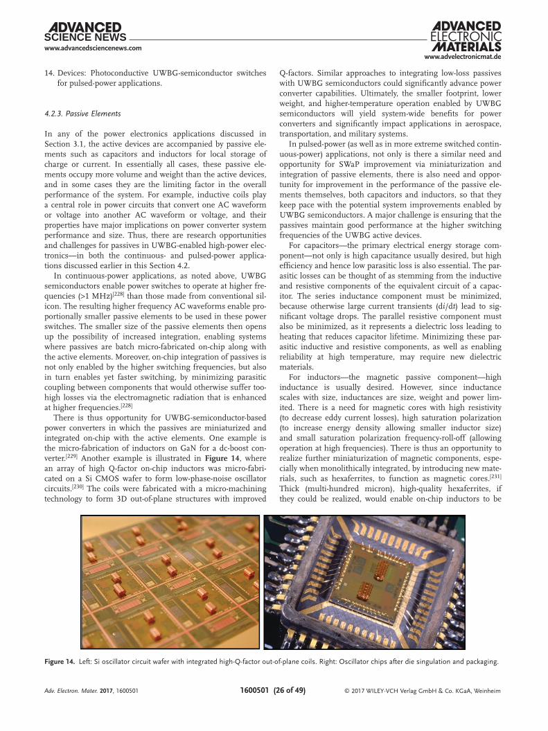
www.advancedsciencenews.com
© 2017 WILEY-VCH Verlag GmbH & Co. KGaA, Weinheim1600501 (26 of 49)
www.advelectronicmat.de
14. Devices: Photoconductive UWBG-semiconductor switches for pulsed-power applications.
4.2.3. Passive Elements
In any of the power electronics applications discussed in Section 3.1, the active devices are accompanied by passive ele-ments such as capacitors and inductors for local storage of charge or current. In essentially all cases, these passive ele-ments occupy more volume and weight than the active devices, and in some cases they are the limiting factor in the overall performance of the system. For example, inductive coils play a central role in power circuits that convert one AC waveform or voltage into another AC waveform or voltage, and their properties have major implications on power converter system performance and size. Thus, there are research opportunities and challenges for passives in UWBG-enabled high-power elec-tronics—in both the continuous- and pulsed-power applica-tions discussed earlier in this Section 4.2.
In continuous-power applications, as noted above, UWBG semiconductors enable power switches to operate at higher fre-quencies (>1 MHz)[228] than those made from conventional sil-icon. The resulting higher frequency AC waveforms enable pro-portionally smaller passive elements to be used in these power switches. The smaller size of the passive elements then opens up the possibility of increased integration, enabling systems where passives are batch micro-fabricated on-chip along with the active elements. Moreover, on-chip integration of passives is not only enabled by the higher switching frequencies, but also in turn enables yet faster switching, by minimizing parasitic coupling between components that would otherwise suffer too-high losses via the electromagnetic radiation that is enhanced at higher frequencies.[228]
There is thus opportunity for UWBG-semiconductor-based power converters in which the passives are miniaturized and integrated on-chip with the active elements. One example is the micro-fabrication of inductors on GaN for a dc-boost con-verter.[229] Another example is illustrated in Figure 14, where an array of high Q-factor on-chip inductors was micro-fabri-cated on a Si CMOS wafer to form low-phase-noise oscillator circuits.[230] The coils were fabricated with a micro-machining technology to form 3D out-of-plane structures with improved
Q-factors. Similar approaches to integrating low-loss passives with UWBG semiconductors could significantly advance power converter capabilities. Ultimately, the smaller footprint, lower weight, and higher-temperature operation enabled by UWBG semiconductors will yield system-wide benefits for power converters and significantly impact applications in aerospace, transportation, and military systems.
In pulsed-power (as well as in more extreme switched contin-uous-power) applications, not only is there a similar need and opportunity for SWaP improvement via miniaturization and integration of passive elements, there is also need and oppor-tunity for improvement in the performance of the passive ele-ments themselves, both capacitors and inductors, so that they keep pace with the potential system improvements enabled by UWBG semiconductors. A major challenge is ensuring that the passives maintain good performance at the higher switching frequencies of the UWBG active devices.
For capacitors—the primary electrical energy storage com-ponent—not only is high capacitance usually desired, but high efficiency and hence low parasitic loss is also essential. The par-asitic losses can be thought of as stemming from the inductive and resistive components of the equivalent circuit of a capac-itor. The series inductance component must be minimized, because otherwise large current transients (di/dt) lead to sig-nificant voltage drops. The parallel resistive component must also be minimized, as it represents a dielectric loss leading to heating that reduces capacitor lifetime. Minimizing these par-asitic inductive and resistive components, as well as enabling reliability at high temperature, may require new dielectric materials.
For inductors—the magnetic passive component—high inductance is usually desired. However, since inductance scales with size, inductances are size, weight and power lim-ited. There is a need for magnetic cores with high resistivity (to decrease eddy current losses), high saturation polarization (to increase energy density allowing smaller inductor size) and small saturation polarization frequency-roll-off (allowing operation at high frequencies). There is thus an opportunity to realize further miniaturization of magnetic components, espe-cially when monolithically integrated, by introducing new mate-rials, such as hexaferrites, to function as magnetic cores.[231] Thick (multi-hundred micron), high-quality hexaferrites, if they could be realized, would enable on-chip inductors to be
Adv. Electron. Mater. 2017, 1600501
Figure 14. Left: Si oscillator circuit wafer with integrated high-Q-factor out-of-plane coils. Right: Oscillator chips after die singulation and packaging.

www.advancedsciencenews.com
© 2017 WILEY-VCH Verlag GmbH & Co. KGaA, Weinheim1600501 (27 of 49)
www.advelectronicmat.de
made significantly smaller. Other materials that may have good properties at higher frequencies include FeN and emerging Fe-based nanocomposites.
15. Devices: New dielectric and magnetic materials and archi-tectures that enable high-frequency ultra-compact integrated passive elements, which in turn enable system performance not limited by performance of those passive elements.
4.3. Radio-Frequency (RF) and Microwave Electronics
UWBG semiconductors have the potential to impact high-fre-quency technologies as well, in particular technologies for gen-erating, switching and receiving high-power RF and microwave signals. Here, we discuss four different ways they might have impact. First, they can serve as either sources or amplifiers of high-power RF signals, most often feeding an antenna. Second, they can serve as a fast switch that connects or disconnects an RF source and receiver to or from an antenna. Third, they can serve as resonant filters for processing RF signals. Fourth, they can serve as the basis for new vacuum electronics architec-tures, of interest for microwave power and thermionic energy conversion.
4.3.1. RF Source Power
Radio-frequency power transistors are required for electronic systems that transmit signals into air or space, with applica-tions ranging from communications to imaging to sensing. For all of these applications, a high output power is usually desired as it improves signal/noise ratio. In addition, the efficiency of power usage (often defined as radiated power out/prime power in) is generally important for all systems, because the non-radiated power is lost as heat which must be removed to avoid overheating the system. Additionally, a system with low efficiency requires excessive prime power that, for systems that use batteries, shortens battery life.
Transistors based on Si, GaAs, and more recently GaN have been the workhorses to date for these power applications,[232] but a consideration of the fundamental materials properties from Table 2 for Ga2O3, high Al-content AlGaN, AlN, BN, and diamond shows that these UWBG materials offer even greater promise for RF applications.
First, power output is proportional to the product of the maximum usable voltage across the output of the device times the maximum allowed current through the device, and both the voltage and current are governed by material properties. The maximum voltage is determined by the critical electric field (EC) for the material in the given device geometry and doping concentration; and the maximum current is determined by the carrier sheet density (ns) and the saturation velocity (vsat) of the electrons or holes.
A higher-breakdown-field material offers two possible advantages for high-frequency transistors. First, for a given drift-region length and fT, a higher breakdown material will support a higher output voltage and therefore more output power. Alternatively, if output voltage is held fixed, the drift region length can be reduced, which leads to a smaller delay
and therefore higher power gain at a given frequency. At a given supply voltage, highly-scaled ultrawide-bandgap transis-tors could therefore provide gain at much higher frequencies than GaN transistors. This gain can be used not just to increase the power-added efficiency at the signal frequency, but also to realize new switched-mode amplifier designs that can go beyond the efficiency limits of class A/B amplifiers.
Since power transistors typically generate heat in their active region that must be removed to avoid exceeding a maximum junction temperature for reliable operation, the thermal con-ductivity is an additional material parameter that is important. As mentioned in the Introduction, the Johnson figure of merit (JFOM) is often used to compare the promise of materials for RF power, and is given in Table 4 together with thermal con-ductivity as key indicators of the potential of the respective UWBG materials for RF power, with Si and GaN given for comparison. It should be noted that existing GaN-based devices already face challenges with heat removal at high power levels and have used diamond layers for heatsinking.[233–237] Devices made of AlGaN, AlN, and especially Ga2O3 will likely also need to be bonded to diamond heatsink layers for thermal manage-ment. Materials such as c-BN and diamond that offer not only high potential power capability but high thermal conductivity in the same material could be especially advantageous for next-generation RF power devices. Therefore, a key research oppor-tunity/challenge is:
16. Devices: Thermally managed UWBG RF transistors that generate higher output powers and power densities than present Si-, III-V-, SiC-, and GaN-based devices.
The higher power densities may be realized via higher volt-ages and/or higher current densities. Both lateral (FET) and vertical (bipolar or FET) designs may be viable here.
4.3.2. RF Switching
In all RF transmitter/receiver architectures there needs to be some means for preventing the high-power output signal from leaking into the receiver input and burning it out. Traditionally, ferrite circulators have been used, but they are bulky and heavy
Adv. Electron. Mater. 2017, 1600501
Table 4. Johnson figures of merit (JFOMs) for UWBG semiconduc-tors, calculated from underlying properties taken from UWBG Material/Device Properties Table 2.
Material vsat (107 cm s−1)
EC at ND = 1016 cm−3 (MV cm−1)
Thermal conduc-tivity (W m−1 K−1)
JFOM (1012 V s−1)
Si 1.0 0.3 145 0.48
GaN 1.4 4.9 253 11.0
AlN 1.3 15.4 319 31.9
β-Ga2O3 1.1 10.3 27 18.0
c-BN unknown 17.5 940/2145 –
Natural/Isotop.
pure
Diamond 2.3 (e−) 13.0 2290/3450 47.6 (e−)
1.4 (h+) Natural/Isotop.
pure29.0 (h+)

www.advancedsciencenews.com
© 2017 WILEY-VCH Verlag GmbH & Co. KGaA, Weinheim1600501 (28 of 49)
www.advelectronicmat.de
and have been increasingly replaced by FETs used as switches to isolate the receiver, as shown in Figure 15.
Similar to the high-frequency power-switching application discussed in 4.2, these devices need a low on-resistance for low RF insertion loss when in the “on” state, and a high-voltage-blocking/low-signal-leakage capability (isolation) when in the “off” state. The relevant figure of merit is (RonCoff)−1, where Ron and Coff are the on and off-state resistance and capaci-tance, since minimizing Ron minimizes the insertion loss and minimizing Coff minimizes the RF feedthrough and switching time.
As UWBG transistors are developed and integrated into power transmitters (the ‘TX’ in Figure 15), their higher output power and voltage will require that the lower transistor switch in Figure 15 be made from the same or similar materials to hold off the higher voltage generated by the transmitter in order to prevent it from burning out the receiver input (the ‘RX’). Therefore, RF switch development must track the advances in RF power-transistor development in the UWBG materials, and the switches can typically either use the same material as their power-device counterpart but with a slightly different design for higher voltage-standoff margin, or use a higher-bandgap alloy (or material) in a similar design. Ron is minimized by using materials having high mobility, and Coff is minimized by using lower permittivity materials that also yield a small device area as discussed previously in Sections 1 and 4.2. Traditionally, with Si-, GaAs-, and GaN-based switches, the on/off isolation ratio only needed to be ≈30 dB or slightly better to prevent burnout of the receiver, but with the higher potential voltages and output powers of future UWBG tran-sistors, this specification will likely need to be raised by many dB, which presents additional challenges in the design of the switching devices and circuits. Thus, another key research opportunity/challenge is:
17. Devices: High-voltage, low-capacitance, low-on-resistance UWBG RF switches having the ability to stand off voltages higher than those generated by UWBG power transistors.
4.3.3. Electromechanical Filters
Electromechanical filters consist of transducers that convert an electrical signal to mechanical motion, which is then passed through a vibrating mechanical system, and then transduced back into electrical energy at the output.
Such filters are widely used in commercial applications: high-performance RF filters based upon physical-vapor-depos-ited PVD-AlN resonators, such as the film bulk acoustic reso-nator (FBAR)[238] and the solidly mounted resonator (SMR),[239] are the dominant technology currently utilized in 4G/LTE (4th generation long-term evolution) communication systems. This is due to their small footprint, high Q-factor, high operating fre-quency, and relatively good power handling.[240–243]
Due to the size and rapidly evolving requirements of the commercial smartphone market, filters used in commercial wireless devices have become lower cost and more compact, and possess improved filter response. This has led to greater overlap in both the requirements and characteristics of filters between commercial smartphones and military Department of Defense (DoD) systems. For instance, all commercial smart-phone filters are thin-film-based resonators and are therefore compact and light. In addition, 4G networks and as-yet unde-fined 5G and internet of things (IoT) future wireless standards have begun to use mm-wave frequencies that overlap with tra-ditional DoD radar bands, ranging from L through Ka bands. Besides decreased size and weight and higher center frequency, the impetus to improve insertion loss and rejection characteris-tics is also common to both commercial and DoD systems.
Note though, that despite the increasing convergence between DoD and commercial piezoelectric filter characteris-tics, the requirements of DoD systems do in fact extend beyond the capability of current commercial filter devices in two impor-tant aspects: power handling and bandwidth.
With respect to power level, commercial surface acoustic wave (SAW) or bulk acoustic wave (BAW) resonator-based fil-ters are typically limited to low power (<2 W), while many DoD applications such as radar and military communication require a combination of decade (10×) wide bandwidth, medium to high power (few W to 100s of W) and low filter loss (<1 dB) at high power. Due to these requirements, many DoD applica-tions cannot use currently available SAW- or BAW-based filters. Instead, they implement the filtering function using either: discrete L and C elements (including varactor-diode-based implementations); transmission-line-based elements; or cavity-, waveguide-, ceramic-, or dielectric resonant oscillator- (DRO) based filters. Each of these approaches has disadvantages in either size or weight, or is forced to make a trade-off between performance versus size and weight.
With respect to bandwidth, cellular communication formats generally possess narrow signal bandwidths (typically <5% fractional bandwidth). This aspect is well-suited to the capabili-ties of filters built using existing thin-film resonators, which use either BAW or SAW vibration modes. However, as formats
Adv. Electron. Mater. 2017, 1600501
Figure 15. Illustration of FETs used as RF switches to separate trans-mitted and received signals in a modern transceiver. Figure courtesy of Randy Wolf, Global Foundries.

www.advancedsciencenews.com
© 2017 WILEY-VCH Verlag GmbH & Co. KGaA, Weinheim1600501 (29 of 49)
www.advelectronicmat.de
move beyond the historical 2.5G and 3G frequency bands and into the higher frequency 4G/LTE bands, requirements become more challenging due to larger fractional bandwidth require-ments.[244] Because the bandwidth of an RF filter is primarily fixed by the electromechanical coupling efficiency of the reso-nator, and since the electromechanical coupling efficiency in turn depends on the piezoelectric constant of the material used to facilitate the conversion of electrical to acoustic energy during operation, increasing the piezoelectric constant is of great interest.
In the incumbent poly-crystalline PVD-AlN-based reso-nator technology, the relatively low effective electromechanical coupling coefficient, eff
2k (e.g. 6–7%), can be attributed to the low piezoelectric constant, e33, of the PVD-AlN thin-film itself. Recent studies have demonstrated that the piezoelectric coef-ficient of PVD-AlN films can be increased by alloying with scandium (Sc),[245,246] or by co-doping of AlN using Mg-Zr or Mg-Hf.[247] However, the process of doping PVD-AlN has other drawbacks that degrade the Q-factor of the resonator.
A particularly promising alternative approach to improving piezoelectric constants is to move beyond polycrystalline mate-rials and to explore crystallographically oriented single-crystal undoped AlxGa1−xN films synthesized via metal-organic chem-ical vapor deposition (MOCVD). While early work has been pub-lished on AlGaN films for acoustic resonators, those results may have been limited by the fabrication processes[248–250] or mate-rial quality.[251] Recently, simulations of AlN acoustic resonators using undoped PVD AlN and undoped MOCVD-AlN predicted significant benefits of using highly oriented, single-crystal AlN films with high e33.[252] Further, recent results on single-crystal MOCVD-AlGaN piezoelectric films on silicon substrates were demonstrated as a preliminary stepping-stone to MOCVD-AlN.[253] Thus, a key research opportunity in this area is:
18. Devices: Single-crystal AlGaN and AlN electromechanical RF filters with very high bandwidth and power-handling capability, small size and weight, and potential for mono-lithic integration with AlGaN electronics.
Some of the performance and reliability advantages of such single crystal III-N resonator technology for resonator and filter applications are illustrated in Figure 16a. Potential spe-cific research directions follow from these potential advantages. These research directions include direct materials characteri-zation to understand the piezoelectric, acoustic and thermal material properties of the single-crystal materials. By building and characterizing resonators and filters fabricated from single-crystal materials, the proposed advantages of single-crystal-based resonators and filters can be explored with respect to improved filter bandwidth, improved filter power handling, improved filter ruggedness and survivability and higher fre-quencies of operation.
Moreover, with the III-N materials, resonator eff2k can be tai-
lored by varying Al composition, as shown in Figure 16b. The ability to tailor resonator eff
2k allows optimal realization of fil-ters with widely varying bandwidths, thus mitigating the design trade-offs inherent when fixed resonator eff
2k is utilized to design filters with widely varying bandwidth. In recent work, resona-tors with a eff
2k of 4.44% and Q of 1277 using 40% AlxGa1−xN films on <111> Si have been fabricated.[253]
Finally, we mention that in the long-term, the ability to use single-crystal AlGaN or AlN in RF MEMs also brings the pos-sibility of integrating this high-performance crystalline piezo-electric material directly with RF electronics. This, in turn, would open up new possibilities for integrated RF switches, filters, MIMs, and optomechanics.
4.3.4. Vacuum Electronics
Vacuum electronics technology is still the most efficient tech-nology for generation of very high microwave power, with applications ranging from the cavity magnetrons that generate power for kitchen microwave ovens, to the traveling-wave tubes (TWTs) that serve as amplifiers in radars and satellite tran-sponders.[254] Vacuum electron emission is also a key element of thermionic energy conversion (TEC). While TEC is not a power electronics technology, it is discussed in this section due to its dependence on low work function surfaces.
The ways in which UWBG semiconductors could make impact on vacuum electronics technology include three general areas, outlined below.
Power Electronics: A first way that UWBG semiconductors could make an impact is in the high-power and RF electronics, discussed throughout Sections 4.2 and 4.3, necessary to drive the vacuum electronics. Improvements in these electronics will result in improved system-level reliability, size, weight and power, as well as enable new concepts such as microwave power modules.
Electron Emitters: A second way that UWBG semiconductors could make an impact is as electron-emitting cathodes for the vacuum electronics device itself. Indeed, the electron-emitting cathode is the heart of vacuum electronics, and replacement of thermionic emission hot cathodes with field emission cold cath-odes has been a longstanding goal for the vacuum electronics community for decades. Improved lifetime and efficiency are the key motivators, but rapid turn-on and pulsed operation ena-bled by near-ambient temperature operation are also motiva-tors. As an example, direct vacuum electron emission has been established from forward-biased diamond-based PiN diodes; these devices could be employed in very high voltage (>10 kV) switches or TWT cathode designs (Figure 17).[49,255]
Interest in using UWBG semiconductors for electron emis-sion can be traced to early measurements of efficient electron emission from diamond surfaces stimulated by above-bandgap light.[256] The measurements were related to a negative electron affinity (NEA) of the hydrogen-terminated surface, and could be described by theoretical analysis of the dipole due to the CH bonding.[257]
Since then, there have been many studies of electron field emission from various forms of diamond, both thin-film and single-crystal. For thin films, while hydrogen termination seems to lead to an improvement of the effect, many results have been related to defects and the presence of sp2-bonded regions in the films. These structures have been used for field-emission cathodes and diodes. For single crystals, there have been a number of reports of diodes that show electron emis-sion from hydrogen-terminated surfaces where the surface included the interfaces of the PiN junction. The early work by
Adv. Electron. Mater. 2017, 1600501

www.advancedsciencenews.com
© 2017 WILEY-VCH Verlag GmbH & Co. KGaA, Weinheim1600501 (30 of 49)
www.advelectronicmat.de
Geis and co-workers employed[258] a carbon-implanted layer to inject electrons into the junction that was fabricated on a p-type base layer. With the development of in-situ phosphorus doping, diamond PiN diode structures have been fabricated that display electron emission from hydrogen-terminated NEA surfaces. Reports have shown emission efficiencies that approach 2.5% of the diode current, similar to the efficiency of thermionic cathodes.[49,50]
There is also interest in other UWBG materials for elec-tron emission. A negative electron affinity has been found for hydrogen-terminated c-BN,[259] and ammonia-exposed surfaces of AlN have shown an electron affinity of less than 1 eV.[260] The AlN surfaces are particularly sensitive to exposure to oxygen,
which increases the electron affinity. Research is yet to establish whether structures fabricated from c-BN or AlN could achieve electron emission, and to date electron emission diodes have not been reported for these materials.
Electron Collectors for Thermionic Energy Conversion: A third way that UWBG semiconductors could impact vacuum elec-tronics is as low-work-function collector surfaces in thermionic energy conversion (TEC) devices. In these devices a low-work-function surface is heated such that it emits electrons, which transit a vacuum gap to a low-work-function collector surface. A direct analysis of the energy-conversion efficiency suggests that a collector work function of 0.5 eV could lead to a TEC with performance that would be similar to a thermoelectric energy
Adv. Electron. Mater. 2017, 1600501
Figure 16. a) Advantages of single-crystal electromechanical resonators for high power, large bandwidth, extreme ruggedness and survivability, and high center frequency. b): eff
2k as a function of Al composition, highlighting increased bandwidth and design.

www.advancedsciencenews.com
© 2017 WILEY-VCH Verlag GmbH & Co. KGaA, Weinheim1600501 (31 of 49)
www.advelectronicmat.de
conversion device with a thermoelectric figure-of-merit (ZT) of nearly 10.
There has been a search for low-work-function surfaces that could be anticipated from NEA surfaces of UWBG materials. Several studies of H-terminated nitrogen-doped single-crystal diamond surfaces have shown thermionic emission with a work function of ≈2 eV.[261] The value is higher than anticipated, and has been attributed to the deep donor level for nitrogen (1.7 eV) and the presence of upward band bending. Studies of thermionic emission from polycrystalline n- and p-doped dia-mond have shown exceedingly low work functions of 1.4 and 0.9 eV, respectively.[262] It has been speculated that the band-bending is mitigated by the high doping density and the pres-ence of grain boundaries. A key research challenge/opportunity here is:
19. Devices: Negative-electron-affinity and/or ultra-low-work-function surfaces for robust, high-electron-emission effi-ciency cold cathodes and/or electron collector surfaces.
4.4. Deep-UV Optoelectronics
As history has repeatedly shown, the principal applications of new materials are often not technologies that they replace, but technologies that they create. In that sense, deep-ultraviolet (DUV) photonic applications are a primary raison d’etre for UWBG materials and will potentially drive many advances.
Optical sources that emit in the deep UV have a wide range of applications, both commercial and military. One set of appli-cations requires bulk “broadband” photons—lots of photons, without the need for single-wavelength operation or narrow linewidths. Another set of applications requires somewhat fewer but “narrowband” photons, more precisely tailored and coherent so as to enable, for example: Raman spectroscopies; non-line-of-sight communication; or resonant interaction with specific atomic absorption lines of interest to sensing and quantum information processing schemes (Section 4.5).
In this Section 4.4, we discuss first broadband photon devices and applications; second, narrowband photon devices
and applications; and third, opportunities and challenges associated with the most mature deep UV material system, AlGaN.
4.4.1. Broadband Photon Emitters and Detectors
Applications for broadband photons include air/water/surface/food purification-disin-fection, materials and polymer processing/curing, medical/biomedical diagnostics and treatment, and scientific instrumentation.
Traditional sources in the UV include mercury lamps, gas lasers (e.g., excimer) and solid-state (e.g., frequency-multiplied Nd:YAG) lasers. Generally, these commer-cial sources are of limited applicability due to poor SWaP characteristics (e.g., they are bulky, heavy, expensive, and inefficient,
require high-voltage operation, and have limited lifetime). Moreover, the use of mercury leads to significant environ-mental pollution issues.
In contrast, optoelectronic devices based on UWBG semicon-ductors would have excellent SWaP characteristics. And, among the UWBG semiconductors, perhaps the best suited is AlN/AlGaN, which is chemically and physically robust, has a direct bandgap over its entire alloy composition, and has the potential for high-temperature operation. The challenge for the UWBG semiconductors is to achieve, in the UV-B (315–280 nm) and UV-C (280–200 nm) spectral bands, performance and efficien-cies similar to those that have been demonstrated in the vis-ible range with the narrower bandgap InGaN material system. Figure 18 shows the reported external quantum efficiencies (EQEs) for LEDs at wavelengths from the violet into the deep UV. The data show that EQE can be quite high (>25%) at wave-lengths >370 nm, with InGaN active layers, but that it drops off steadily for wavelengths <360 nm, with AlGaN active layers, and drops off precipitously at wavelengths below 250 nm. The notable exception is for LEDs near 270 nm with 10% EQE, where significant investment has been made to address germi-cidal applications such as water purification and fluorescence detection of biomolecules.
Ultimately, power efficiency, commonly referred to as wall-plug efficiency (WPE), in the range of 10% is likely necessary, combined with useful output power and competitive cost, to enable economical industrial-scale applications of UV LEDs. (Note that EQE tracks the efficiency for converting injected electrons into emitted photons while WPE records the conver-sion of electrical power into optical output power and includes series resistance losses; thus WPE ≤ EQE.)
Finally, we note that solar-blind UV-C photodetectors are also of interest for various applications in commercial gas furnaces, as well as military non-line-of-sight, short-distance, secure com-munications and several other threat-detection systems. While AlGaN UV photodetectors are commercially available, AlGaN-based avalanche photodiodes (APDs) are still in an early stage of development. Of the available UWBG semiconductors, AlxGa1−xN is perhaps best suited for fabricating UV-C light
Adv. Electron. Mater. 2017, 1600501
Figure 17. Left: Cross-section schematic of an electron-emission diamond diode. Right: Image of fabricated electron-emission diode (on-state) and measurement probes. The electrolumi-nescence originates from defects and was only observed at forward bias. Reproduced with permission.[49] Copyright 2013, John Wiley and Sons.

www.advancedsciencenews.com
© 2017 WILEY-VCH Verlag GmbH & Co. KGaA, Weinheim1600501 (32 of 49)
www.advelectronicmat.de
emitters and detectors, due to its chemical/physical robustness, potential for high temperature operation, ability to form hetero-structures, and a direct bandgap over the entire alloy composi-tion range.
4.4.2. Narrowband Photons: Chemical Sensing and Quantum Information
The dominant applications for which narrowband deep-UV photons are desirable are chemical sensing and quantum infor-mation. For chemical sensing, a deep-UV laser source would be highly desirable to enable point-of-need identification of bio-chemicals by Raman spectroscopy, which requires select wavelengths (<240 nm), high power, and high beam quality in a compact, rugged system. For quantum information, as discussed below in Section 4.5, narrowband laser photons enable the interrogation of quantum systems with very narrow transitions.
Two features are important for these applications.The first feature is the emission of much shorter wave-
lengths than are currently possible. Attempts to realize elec-trically-pumped pn-junction diode lasers in the deep UV have been frustrated by materials, physics and device challenges similar to those faced by deep-UV LEDs: these are discussed below. To date, the shortest wavelength that has been achieved in an AlGaN-based diode laser is 336 nm.[264]
The second feature is, in some cases, ultra-narrow linewidths. These would require single-longitudinal-mode operation, and thus low-loss narrowband distributed Bragg reflectors (DBRs) for vertical-cavity devices or distributed feedback (DFB) grat-ings for horizontal (edge-emitting) devices. Fabrication of these will be challenging. The required pitch for a half-wavelength grating fabricated in AlN (n = 2.32) at a wavelength of 275 nm, for example, is only 60 nm.
4.4.3. AlGaN Materials, Physics and Device Challenges
The materials, physics and device challenges associated with deep-UV LEDs and/or lasers are non-trivial. Because AlGaN
semiconductors are the most mature of the UWBG semicon-ductors for these applications, we discuss them in some detail here. AlGaN semiconductors are far more challenging than their lower-bandgap InGaN and other counterparts used in vis-ible/IR optoelectronics, though, in four key ways.
First, p-type dopants in AlGaN, typically Mg acceptors, present a number of difficulties. As has been discussed in Section 2.5, Mg acceptors in AlGaN are very deep, with ioni-zation energies well over 150 meV, thus making p-doping, especially of high Al-content (x > 0.4) AlxGa1−xN, fairly diffi-cult. Also, because of high UV optical absorption of p-AlGaN, light extraction and external quantum efficiency are decreased. Furthermore, because p-type doping concentrations are lim-ited, cladding layers must be relatively thin to minimize series resistance, but then the optical confinement necessary for effi-cient laser diodes is poor. Therefore, the well-developed device designs commonly used for IR-visible lasers cannot be used. This has spurred interest in alternative semiconductor laser configurations, in particular approaches that can circumvent the need for p-doped AlGaN layers. For example, an alternative approach to edge-emitting laser diodes for deep-UV emission is the use of a vertical external cavity surface emitting laser with an AlGaN gain chip that is pumped with a high-energy electron beam; this architecture bypasses the p-doping issue and can realize high beam quality (spectrally and spatially).[41]
Second, in high-Al-content (x > 0.4) and highly-ionic AlxGa1−xN materials, spontaneous and piezo-polarization fields are very high. This leads to a number of deleterious conse-quences, including a spatial separation in the electron and hole wave functions that decreases the electron-hole recombination rate.[265]
Third, no electrically conducting and optically transparent substrates are available for the UWBG III-N materials. Bulk AlN substrates, despite their insulating nature, are probably one of the best technical choices, due to their high crystal-line perfection for epitaxial growth. However, as discussed in Section 2.1, they are still in the developmental stage, and obtaining a large number of them with fixed specifications for systematic studies is currently cost prohibitive.
Fourth, for vertical light-emitting devices, a phenomenon called TE/TM polarization switching becomes important.
Adv. Electron. Mater. 2017, 1600501
Figure 18. Reported external quantum efficiencies for AlGaN, InAlGaN, and InGaN quantum-well LEDs emitting in the UV spectral range.[263]

www.advancedsciencenews.com
© 2017 WILEY-VCH Verlag GmbH & Co. KGaA, Weinheim1600501 (33 of 49)
www.advelectronicmat.de
This phenomenon is due to a materials aspect of AlGaN that is not true of InGaN: GaN and AlN feature a different sign in their crystal field splitting. Whereas it is negative for AlN, it is positive for GaN, so the ordering of the valence bands differs between AlN and GaN. Thus, light generated within a GaN layer is predominantly TE polarized with an electric field vector E perpendicular to the c-direction, while light generated within an AlN layer is predominantly TM polarized with E parallel to the c-direction. For ternary AlGaN materials as used in UV light emitters, a transition from TE to TM polarization occurs as the Al concentration increases.[266] Since TM-polar-ized light cannot be extracted parallel to the c-direction (the most commonly used growth direction for III-N materials), the performance of vertically-emitting UV LEDs degrades as Al content increases and wavelength decreases. Vertically-emitting lasers would be similarly affected. Moreover, since TM-polarized light is generally not as tightly confined as TE-polarized light, TM optical modes interact more strongly with, and experience slightly higher optical absorption by, the p-type confinement layers in laser heterostructures. Thus, the performance of edge-emitting UV laser diodes would also be expected to experience performance degradation with TM optical modes.
Mitigating the issues listed above will not only lead to more efficient UV-C emitters and detectors, it will also improve UWBG RF and power electronic devices. Non-conventional doping schemes such as 3D superlattice doping and polarization-assisted doping can potentially be used to significantly increase the p-doping concentration in high-Al-content AlxGa1−xN layers.[267] The issue of light extraction and hole transport might also be addressable through the use of interband tunnel junctions.[206] New device designs and material deposition approaches to manage the strain and polarization in UWBG heterostructures are also being explored with some initial suc-cess. To overcome the bulk AlN substrate issue, new approaches are needed to create thick and low-defect-density free-standing AlN substrates to replace inferior but readily available UV-C transparent substrates such as sapphire. These can also provide a very useful platform for systematic research.
Taken together, an overarching Research Opportunity/Chal-lenge for UWBG optical emitters is:
20. Devices: LEDs with >10% wall-plug efficiency at wavelengths <260 nm; and compact laser sources in the UV-C and UV-B bands with power efficiency >10% and high beam quality.
4.5. Quantum Information
Quantum information science is a rapidly evolving global field of investigation with the potential to impact multiple techno-logical areas, including: position determination, navigation and timing; tunnel detection; encryption code-breaking; secure communications; advanced simulation and high-speed compu-tation; and magnetic anomaly detection.[268] UWBG semicon-ductors have potential roles in quantum information science in two substantial ways: as transparent hosts for dopants and defects with electronic/spin states suitable for quantum infor-mation processing; and as a photonic platform for quantum processors either based on linear optical quantum computation
(LOQC) in which photons serve as the qubits, or for state manipulation in systems based on trapped-ion qubits.
4.5.1. Host for Quantum States
A first potential role for UWBG semiconductors is as the host for electronic/spin states sufficiently decoupled from the lat-tice to be long-lived and whose transitions are extremely sharp, yet able to be externally interrogated. Prototypical systems are the nitrogen-vacancy (N-V) or silicon-vacancy (Si-V) centers in diamond, which display long spin relaxation times and can be interrogated optically. These systems were among the first to be considered for quantum information, and continue to be an active area of research,[269] with new developments emerging, including the possibility of incorporating these centers into dia-mond devices where a gate bias controls the charge state of the center and affects its quantum characteristics.[115,270]
Note that here the challenges are very different from those mentioned in Section 2.5. There, the purpose of doping or defect incorporation is to create free carriers, and the depth of the defect levels in the UWBG semiconductors makes this challenging. In contrast, here one is intentionally interested in dopant and defect states that are deep in the bandgap and suf-ficiently decoupled from the host UWBG lattice so as to sustain long lifetimes, and thus minimize inhomogeneous broadening of their quantum states.
Also note that, while cubic (or at least covalent) materials are considered to be desirable because higher symmetry leads to better performance in nanodevices with respect to more light in the zero-phonon line, recent theoretical work on wurtzite AlN suggests that point-defect complexes could act as qubits and that manipulation of its piezoelectric properties through biaxial or uniaxial strain could enable nitrogen-vacancy centers as potential qubits.[271,272] Moreover, rare-earth ions (Nd) doped into AlN may also be a candidate for quantum memories. In this case, it is critical to control inhomogeneous broadening of the dominant rare-earth dopant optical transition, which can be aided by substitutional doping using plasma-assisted MBE, for which it has been shown that the vast majority of Nd dopants (>95%) take the majority site.[273]
Other possibilities for UWBG-semiconductor-based quantum information systems could involve valley-polarized electrons (i.e. “valleytronics”) or superconductivity, both of which have been reported in diamond. The long electron life-time for indirect-bandgap diamond, and the different effective mass for the different k-space propagation directions, can sup-port changing the concentration of electrons in the six conduc-tion band valleys.[274] With heavy B-doping, metallic conductivity can be achieved, and superconductivity has been established at temperatures near 11 K. There may be other structures that can achieve a superconducting state involving the diamond valence band electrons, as well.
4.5.2. Photonic Platform for Interrogation of Quantum States
A second potential role for UWBG semiconductors is as a photonic platform for the generation, manipulation, and
Adv. Electron. Mater. 2017, 1600501

www.advancedsciencenews.com
© 2017 WILEY-VCH Verlag GmbH & Co. KGaA, Weinheim1600501 (34 of 49)
www.advelectronicmat.de
interrogation of quantum states. Indeed, all of the neces-sary photonic building blocks could potentially be based on UWBG semiconductors, and in particular on AlN/AlGaN: narrow-linewidth lasers, high single-photon-detection efficiency avalanche photodiodes, waveguides for photonic integrated cir-cuits, and nonlinear optical media for wavelength conversion to spectral regions more suitable for low-loss transmission of photon-based quantum information (i.e., the 1300–1600 nm tel-ecom band).
Tables 5 and 6 contain the reported and desired values of a number of material and device parameters that are relevant to linear-optical and trapped-ion quantum-computing architec-tures. In LOQC systems,[275] the quantum information is rep-resented by the states of single photons, and these states are manipulated by linear optical elements (e.g., beam splitters, phase shifters, and mirrors). In trapped-ion quantum proces-sors, the quantum information is contained in the states of the ions,[276] and these states are typically initiated and read out by exciting each ion with lasers at a number of different wavelengths. We note that photon-based quantum information systems depend strongly on the transition wavelengths of the atoms or defect states used in these systems. Also note that the parameters shown in Tables 5 and 6 are representative of the
values currently thought to be needed, but will certainly evolve in the future.
The tantalizing research opportunity/challenge here would be an integrated photonic platform containing all the building blocks necessary for the generation, manipulation, and inter-rogation of quantum states:
21. Devices: A photonic integrated circuit incorporating all the building blocks (e.g., UWBG lasers, AlN waveguides, AlGaN/SiC detectors) necessary for a single-chip quantum information processing system (based on trapped ions, neutral atoms, photons, or defect centers).
A first building block would be the narrow-linewidth (≈MHz to as small as <10 Hz) lasers necessary for manipulation of quantum systems such as trapped ions, as well as many other applications in atomic, molecular, and optical (AMO) physics, including laser cooling, optical trapping, atomic clocks, etc. These lasers need to be single-longitudinal-, single-transverse-mode with a range of powers from mWs (optical cycling through dipole transitions for laser cooling and fluorescence detection, as well as photoionization) to watts (Raman transi-tions for coherent gate operations involving multiple qubit gates). Some of the required lasers for trapped ions are in the ultraviolet—thus the importance of UWBG semiconductors, though frequency-multiplied optically pumped semiconductor lasers (OPSLs) are starting to find use here.[288] A potential can-didate for the required lasers would be UWBG vertical-external-cavity surface-emitting lasers (VECSELs) with the power (watts) and narrow linewidths necessary to address the relevant transi-tions in ions.[288]
A second building block would be single-photon-counting detectors with high quantum efficiency (>70%) and concomi-tant high single-photon detection efficiency (>40%), required to work in conjunction with these lasers for both the optical cycling fluorescence measurements and the Bell state meas-urements required to verify entanglement of trapped ions. While previous work suggests that SiC may be capable of this performance in the UWBG 260–280 nm range,[289] hybrid(Al)GaN/SiC detectors that extend the high quantum efficiency of SiC to shorter wavelengths through mitigation of sur-face effects,[290] and to longer wavelengths through separate absorption and multiplication structures,[291] will likely also play a role.
Adv. Electron. Mater. 2017, 1600501
Table 6. Material and device parameters of interest for trapped-ion quantum-computing architectures.
Parameter Reported/Demonstrated Required Value
Value Wavelength [nm] Material
Single-mode Waveguide Optical Loss [dB cm−1] <1, 20a); 30a) 633–1092, 405; 405 SiN; GaN <1 at 370–1100 nm
Linear E-O Coefficient (r13) [pm V−1] 1,[283] 10[284] 633 GaN, LiNbO3 (bulk) 10b) at 400, 700 nm
Photodetector Detection Efficiency [%] 30,[285] 93[281] 422, 1550 Si SPAD, WSi SNSPD >90% at 422 nm
Waveguide Power Handling [dBm] 33[286] 1560 SiN 30–50 @ 400, 700 nm
Optical Amplifier Gain [dB] 20–28[287] 405 GaN 20–30, for monolithically
integrated devices
Single-mode Waveguide Optical Loss [dB cm−1] <1, 20a); 30a) 633–1092, 405; 405 SiN; GaN <1 at 370–1100 nm
a)Measurements at MIT Lincoln Laboratory, unpublished; b)Assumes a 200 mm long modulator and desired Vp = 10 V.
Table 5. Material and device parameters of interest for linear-optical quantum-computing (LOQC) architectures.
Parameter Reported/Demonstrated Required Value
Value Wavelength [nm] Material
Optical Loss 8 dB cm−1[277] 640 AlN/SiO2 ≈2 dB cm−1
Linear Electro-
Optic Coefficient0.7 pm V−1[278] 628 AlN/SiO2 ≈1 pm V−1
Single-Photon
Emission
Efficiency
72%[279] 920 GaAs/InAs 99%
Maximum
Quantum Emitter
Count Rate
4 × 10⁶[280] 625 h-BN –
Photodetector
Detection
Efficiency
93%[281] 1500 WSi super-
conductor
99%
Isotope Purity 99.99%[282] – Diamond 99.99%

www.advancedsciencenews.com
© 2017 WILEY-VCH Verlag GmbH & Co. KGaA, Weinheim1600501 (35 of 49)
www.advelectronicmat.de
A third building block would be optical waveguides having (i) low loss from UV to near-infrared (NIR) wavelengths, and (ii) large nonlinear optical properties to enable frequency con-version from the ultraviolet to the visible/NIR necessary to enable long-distance entanglement of quantum systems based on a trapped-ion platform (currently the most mature), in which state manipulation normally occurs in the UV. AlN is promising here, since it is both optically transparent and has relatively large nonlinear optical coefficients.[292] Combined with its potential for lasers and detectors, AlN may someday enable photonic integrated circuit platforms for quantum infor-mation processing, including those involving trapped ions.[293]
4.6. Extreme Environment
Extreme environment is another broad class of applications in which UWBG semiconductors can excel. Here, we discuss two broad sub-classes of these applications, in which the envi-ronments are extreme either because of the presence of radia-tion where radiation-hard electronics are necessary, or because of high temperature/pressure or corrosive chemistry where extreme environment sensors and electronics are necessary.
4.6.1. Radiation-Hard Electronics
Cross-cutting many of the technologies and applications already discussed, one great advantage WBG and UWBG technologies possess over silicon technologies is robust-ness in radiation environments. Applications requiring high-voltage, high-current, radia-tion-tolerant power devices include electronic thrust control actuators of rockets and mis-siles (as opposed to hydraulic control), and solar electric propulsion (SEP) of spacecraft. The SEP system envisioned by NASA would enable human exploration missions out-side of earth’s orbit, and requires functional power devices with high blocking voltages, high current capability, and high tolerance for radiation effects.[294] WBG and UWBG materials are also robust for high tempera-ture operation, another advantage for space applications.
To date, almost all available commercial GaN power devices are not sufficiently rated for the high-voltage power conversion envi-sioned by NASA.[295] SiC MOSFETs meet the voltage requirement, but are susceptible to destructive events due to protons and heavy ions in space at a fraction of the maximum rated electrical voltage.[296] In fact, UWBG devices will be required in any application where both radiation hardness and high tem-perature operation are needed, because of the radiation vulnerability of SiC devices. A new generation of UWBG devices could be a
critical enabling technology for the next generation of rockets, missiles, and spacecraft.
There are two main reasons for the radiation hardness of UWBG semiconductor technologies. First is their wider energy gap (EG): this requires higher energy photons or ions transiting the material to achieve ionization of electrons and holes in the semiconductor. Second and just as important is the ability in some UWBG semiconductors to form heterostructures using two layers of materials with different bandgaps to create a region with a two-dimensional electron gas (2DEG), thereby forming a channel in a high electron mobility transistor (HEMT); the channel electron density in such structures is relatively insensi-tive to the impurity doping level, and hence is insensitive to deep levels due to radiation-induced displacement damage effects.
Although MOSFET structures can also be built with UWBG materials, they are not as well suited to radiation environments because of the large depletion regions typically associated with their structure and the gate oxides that collect deposited charge from radiation.
There are four basic kinds of semiconductor radiation effects, and as illustrated in Figure 19, the heterostructure-based HEMT has an advantage over a silicon or silicon carbide MOSFET for each kind of radiation effect.
• Total ionizing dose: TID causes the accumulation of charge in a gate or field oxide resulting from photons or particles pass-ing through the oxide, leading to shifts in threshold voltage
Adv. Electron. Mater. 2017, 1600501
Figure 19. A trench-gate vertical silicon MOSFET (left) and a notional GaN HEMT (right), both biased in the off state with 100 V bias on the drain, approximately drawn to scale. Figure based on a Synopsys Sentaurus TCAD Simulation.[297,300]

www.advancedsciencenews.com
© 2017 WILEY-VCH Verlag GmbH & Co. KGaA, Weinheim1600501 (36 of 49)
www.advelectronicmat.de
or leakage current. The HEMT has a Schottky metal gate, which eliminates most of the TID parameter shifts seen in MOSFETs.
• Single event effects: SEEs are caused by energetic ions passing through the semiconductor, depositing energy and creating electron-hole pairs (EHPs). The EHPs separate and drift or diffuse under the influence of an electric field or a concen-tration gradient, respectively. A HEMT typically has a much smaller depletion region (of order 1 micron for a drain volt-age of 100 V) than Si or SiC MOSFETs for the same applied voltage (on the order of 5 microns for 100 V; see Figure 19). Consequently, less deposited charge is collected in the drain of the HEMT than in the drain of the MOSFET[297] for the same energy ion and transistor bias voltage.
• Similarly, dose-rate radiation effects sensitive to the entire volume of a device can be important. Since the HEMT has a smaller depletion region volume than the MOSFET, less charge is collected and the HEMT photocurrent is smaller, producing less disruption to the transistor behavior.
• The last radiation effect is displacement damage, in which particles such as neutrons or protons displace the semi-conductor atoms from the crystalline lattice, creating traps and recombination sites in the device, or even new isotopes through fission of the original atoms in the lattice. The atom displacement increases scattering of charge carriers and reduces carrier mobility from the pre-irradiated state. Both SiC MOSFETs and GaN HEMTs have been shown to toler-ate neutron or proton radiation to very high fluences,[298,299] much higher than Si MOSFETs.
Finally, there are two destructive effects that occur in Si MOS-FETs that do not occur in HEMTs. Single-event burnout (SEB) occurs when the charge from an energetic ion creates sustained conduction of the para-sitic bipolar transistor inherent in Si MOSFET design (this is an npn bipolar for an n-channel MOSFET; see Figure 19). The bipolar con-duction can cause sufficient current to flow such that the device undergoes thermal damage or destruction. Single-event gate rup-ture (SEGR) occurs when charge build-up near the gate causes a breakdown in the gate oxide, resulting in gate current and the loss of elec-trostatic control of the Si MOSFET.
All of the above advantages of HEMTs apply to both the narrow- (InGaAs) and wide-bandgap (GaN) devices. However, the UWBG materials should improve the immu-nity of HEMT transistors to radiation sig-nificantly further due to their higher critical fields, which should result in smaller devices, thereby reducing the volume for collecting radiation-induced charge due to ions or pho-tons in either single-event or dose-rate envi-ronments. Thus, we envision the following research opportunity/challenge:
22. Devices: UWBG power devices that exhibit essentially no performance
degradation and no destructive single-event effects in radia-tion environments.
4.6.2. Extreme-Environment Sensors/Electronics
Sensors efficiently gather data on the surrounding physical environment for enhanced safety, security and uninterrupted continuity of services, including those provided by critical infra-structure. Extreme environments include high temperature (350 °C to 1000 °C), high pressure (>1000 atmospheres), high shock (>1000 g), extreme mechanical vibration, high radiation (>100 Mrads), erosive flow, corrosive media, electrostatic dis-charge and electromagnetic interference. Such extreme con-ditions can destroy or degrade the performance of sensors, semiconductor electronics, dielectrics and interconnects, while also accelerating almost all aging and failure mechanisms that occur at room temperature, as well as introducing new ones.
As illustrated in Figure 20, traditional Si-based co-located sensors and electronics fall severely short in their performance under extreme conditions and fail to gather data on ambient conditions in systems such as the combustion chambers and exhaust systems of automotive or aviation engines, down-hole environments in deep-well drilling, industrial processing plants, nuclear reactors, re-entry vehicles, and satellites in orbit. Sensing temperature, pressure, vibration, motion or distance at extreme temperatures, determining temperature and radio-activity in high radiation environments, measuring fluid levels and detecting gases and chemicals in high moisture and highly corrosive environments pose a number of challenges.
Unlike consumer electronic devices, which incorporate many sensors, microprocessors, and wireless chipsets, only
Adv. Electron. Mater. 2017, 1600501
Figure 20. Industrial sectors in which extreme-environment sensor technologies are currently used. The technologies are organized by desired operating temperature and increasing sensing system complexity. Current silicon-based sensing systems can operate at a maximum tempera-ture of ≈200 °C.
www.advancedsciencenews.com
© 2017 WILEY-VCH Verlag GmbH & Co. KGaA, Weinheim1600501 (37 of 49)
www.advelectronicmat.de
simple sensors are available for use in extreme environments. There are no microprocessors, wireless electronics or pow-ering devices (batteries) suited for use at extreme temperatures (>250 °C). Today, active cooling is used in applications requiring sophisticated electronics in high temperature environments; however, active cooling is not feasible in applications where low-temperature ambient is not available (e.g., down-hole explo-ration or aircraft engines). In these cases, extended operation at high temperatures is required.
To extend operation to somewhat higher temperatures, silicon-on-insulator (SOI) enabled MOSFET electronics with improved off-state current have been demonstrated to operate at up to 300 °C. GaAs and its alloys, such as AlGaAs-based devices, were also demonstrated to operate beyond 300 °C, though with limited reliability.[301] Furthermore, electronics based on WBG materials such as SiC and GaN have been dem-onstrated to operate beyond 600 °C. However, the density of temperature-induced intrinsic carriers in these materials sur-passes the concentration of dopant-induced carriers at these very high temperatures (beyond 800 °C for SiC and 1000 °C for GaN), degrading device performance.[301–305]
Thus, there is a strong incentive to develop UWBG tech-nology for these extreme environments, perhaps able to with-stand operating temperatures above 1000 °C. A first aspect of this technology is the sensors themselves, including (i) electro-chemical, (ii) optical, (iii) mechanical (MEMS), and (iv) charged-particle-based sensors. These sensors might be discrete or might be integrated with other sensors for multi-component orthogonal sensing in environments that change quickly and contain a number of chemical or biological species.[306,307] A second aspect of this technology is electronics[308]—wireless data communication and power sources[306,309–315] that can be co-located with the sensors.
The challenges in building such integrated sensing/elec-tronics systems are many. Materials-level challenges include material diffusion and intermetallic formation, and temper-ature-gradient-induced mechanical stress. Device-level chal-lenges include high-performance contacts, interconnects, dielectrics, and encapsulation materials for extreme environ-ments; controlled doping; complementary field-effect-transis-tors; and designs that are robust against imperfections (see e.g. Section 4.7). The hope is that new platforms based on lateral and vertical 1D,[307,316] 2D[317,318] or 3D[319] III-N structures will help in overcoming these challenges.
For example, MEMS sensors based on AlGaN can exploit the 2D electron gas (2DEG) that forms at an AlGaN/GaN hetero-junction and that can act as a virtual metal electrode beneath an AlGaN MEMS resonator.[320,321] By employing recent advances in low-dimensional materials synthesis,[322] multiple analytes and physical state variables can be detected in an orthogonal fashion. Complementing electric-current-based transduction, charged particles generated by field emission and field ioni-zation on ultra-sharp semiconductor tips or filaments can be superior transducers for fast, efficient and reliable sensing of gas, pressure, shock and vibration in extreme conditions.[323]
Beyond the integrated sensing/electronics system itself, power delivery to the system is also an important challenge. Present battery technology is limited to an operational tem-perature below 150 °C, and cabled-power wiring dramatically
increases system weight and complexity making it impractical for many harsh environments. For these reasons, energy har-vesting has emerged as a promising power source that can lead to an autonomous integrated sensing module with reduced cost.[324–326] To date, only a few energy harvesting devices for harsh environment applications have been reported using vibration[325,327] and UV.[326] AlN piezoelectric energy harvesters were demonstrated to deliver 80 µW at 300 °C.[325]
Of special interest are beta-voltaic (BV) and alpha-voltaic (AV) devices that efficiently convert radioactivity directly into electrical energy. These devices operate by the creation of elec-tron-hole pairs in rectifying semiconductor junctions by high energy beta (β) and alpha (α) particles, and thus generate power in a manner similar to a photovoltaic (PV) cell. When designed with UWBG materials, these power sources (with lifetimes ≈ 5 to 100 years) can offer high energy density, stability and very high durability to sensing systems in extreme environments (above 1000 °C[328]), providing a superior alternative to chemical batteries, fuel cells, super-capacitors, and radioisotope thermoe-lectric generators. Such sources can power wide-bandgap-based solid-state sensing electronics with capabilities for telemetry.
In this area, an overarching research opportunity/challenge is thus:
23. Devices: A new generation of extreme-environment sensors with co-located power and data processing electronics.
4.7. Processing, Modeling/Calibration, and Packaging
Though technically not a device or application area, here we discuss research opportunities and challenges associated with a key topic that cross-cuts all devices: how they are processed, modeled, calibrated, and ultimately packaged.
4.7.1. Processing
A number of challenges must be overcome if UWBG mate-rials are to be effectively processed and integrated into working devices. In this subsection we discuss the most important pro-cess challenges, including doping (in particular selective area doping), Ohmic contacts, gate insulators, and integration. The overarching research opportunity/challenge is:
24. Devices: Development of an UWBG materials and device processing toolkit, including: selective area doping; low-resistance Ohmic contacts; and materials integration.
Selective-Area Doping: As discussed in Section 4.2, developing vertical device architectures in UWBG materials is critical to high-power electronics (HPE). In turn, such architectures depend on an effective means for lateral selective area doping. Such selective-area doping is required not only for effective edge termination, but also for the fabrication of most vertical device structures more complex than a simple PiN or Schottky diode.
In the mature Si and SiC materials systems, ion implanta-tion is used for lateral doping; indeed, the development of ion implantation for these materials was revolutionary. For com-pound semiconductor materials, including WBG GaN and
Adv. Electron. Mater. 2017, 1600501

www.advancedsciencenews.com
© 2017 WILEY-VCH Verlag GmbH & Co. KGaA, Weinheim1600501 (38 of 49)
www.advelectronicmat.de
UWBG AlN, ion implantation is problematic, though there have been some recent promising reports for n-implantation of GaN coupled[329] with mixed reports for p-implantation (Mg) of GaN.[330] A major issue is that, after ion implantation, annealing of compound semiconductors requires second-nearest-neighbor (not just nearest-neighbor) re-ordering to heal the lattice damage caused by the implantation. This re-ordering requires relatively high annealing temperatures (rela-tive to melting temperatures) that, at least for GaN, cause the problematic sublimation of N out of the crystal. The resulting residual defects, including localized stacking faults, can act as carrier traps,[331] effectively negating the implanted dopant. Note, though, that non-compound UWBG semiconductors such as diamond may not suffer as severely from this issue.
An alternative approach to ion implantation is etch-and-regrowth, where a region that would have been implanted is instead etched, and material of the opposite doping type is re-grown in the etched region. This approach likewise has had its share of difficulties. For example, in one instance researchers attempted to re-grow the channel on an etched current-blocking layer in a CAVET (see Figure 12), but crystalline defects formed near the top corner of the etched-out area.[217] Another example of problems with this approach is that material polarity may impact doping efficacy in regrown areas, as illustrated in Figure 21. Perhaps most importantly, re-grown pn junctions in GaN have thus far failed to exhibit the same electrical quality as in-situ grown junctions, as determined by junction leakage
current. Nonetheless, the demonstration of high-quality selec-tive-area regrowth would be a major step towards realization of robust vertical devices in GaN as well as in UWBG semicon-ductors, in general.
Note that, in conjunction with selective-area regrowth, there are other options for doping within the regrowth areas. In polar materials such as AlGaN, compositional grading introduces a fixed polarization charge in the material, which in turn attracts free carriers from other parts of the structure (e.g., from sur-face states). This technique has in fact been demonstrated for AlGaN graded from 0–30% Al.[333] Another approach is to uti-lize a superlattice in which the polarization-induced electric fields cause ionization of the impurity dopants due to extreme band-bending.[334]
Ohmic Contacts: Ohmic contacts are another significant chal-lenge for UWBG materials. In conventional semiconductors, Ohmic contacts are typically realized by metal–semiconductor junctions in which the potential barrier becomes very thin due to high doping in the semiconductor, and is thus conducive to tunneling. However, as we have seen, achieving high levels of doping in UWBG semiconductors is problematic. Further, due to the wide bandgap and lower electron affinity of UWBG mate-rials, the Schottky barrier heights of common metals such as Pt and Ni are very high (>2 eV),[31,335] resulting in high specific contact resistivity. For AlGaN with 40–60% Al content, specific contact resistivities are typically in the 10−2 to 10−1 Ω cm2 range, while by contrast Ohmic contacts to conventional WBG AlGaN/GaN HEMTs are routinely in the 10−6 Ω cm2 range.[336,337] Exotic metallizations, such as vanadium, have been reported to have specific contact resistivity in the 10−6 Ω cm2 range for AlGaN up to 70% Al composition, but the resistivity rap-idly increases for still-higher Al compositions, peaking around 100 Ω cm2 for AlN.
For the nitrides, once again compositional grading may come to the rescue; here the composition is graded from high-Al-content for the active region of the device down to low-Al-content AlGaN, or even GaN, onto which Ohmic metallization may readily be achieved. This approach has in fact achieved Ohmic contacts with specific contact resistivity in the low 10−6 Ω cm2 range to devices with Al0.75Ga0.25N channels.[338,339]
For UWBG materials for which compositional grading is not possible, metals with a low Schottky barrier height to the semiconductor of interest should be explored, and methods to achieve high doping, as outlined above, should be investigated in parallel.
Integration: Finally, as discussed in Section 3.3, integration of UWBG semiconductor materials will likely be important for optimization of combined thermal and electronic properties. Certainly there has been a significant effort to take advantage of the high thermal conductivity of diamond for high-power GaN HEMT RF devices. There is also a potential advantage to integrating GaN electron devices with diamond-based hole devices. This could be extended to diamond electronics and nitride optoelectronics that are monolithically integrated on the same chip. Such monolithic integration of diamond and III-N materials could potentially be enabled by using epitaxial cubic BN as an intermediary. While there is a large lattice mismatch between c-BN and AlN, the c-BN/AlN interface could exhibit chemical stability and support efficient thermal transport, and
Adv. Electron. Mater. 2017, 1600501
Figure 21. Top: Schematic of a lateral pn junction based on GaN doped with Mg. Bottom: SIMS data of O and Mg incorporation in the Ga-polar and N-polar GaN. Significantly more O is incorporated in the N-polar GaN,[332] illustrating how material polarity can affect dopant and impurity incorporation during growth. Reproduced with permission.[332] Copyright 2007, AIP Publishing.

www.advancedsciencenews.com
© 2017 WILEY-VCH Verlag GmbH & Co. KGaA, Weinheim1600501 (39 of 49)
www.advelectronicmat.de
the epitaxial c-BN/diamond interface might also effectively transfer thermal energy between the layers.
In general, vertical epitaxial heterostructures have proved crucial for compound semiconductor (including current WBG III-N) devices. Such heterostructures will almost certainly be important for UWBG devices as well, if they can be developed. It is easy to imagine these in the AlGaN/AlN system, but they could be just as important in more novel systems such as epi-taxial diamond/c-BN and Ga2O3/Al2O3 heterostructures.
4.7.2. Modeling/Calibration
Device-level technology computer-aided design (TCAD) based finite-element models (such as was used to create Figure 19) are commonly used to solve the coupled equations for carrier transport, heat transport, electrostatics (Poisson’s equation), and trap occupation statistics to predict steady-state or tran-sient spatial distributions of temperature, electric field, free car-riers, and more. Such models, properly built and validated, can be used to understand how variations in device layout, doping concentration in various regions, and various other engineered parameters, determine measurable quantities such as transistor gain, switching speed, optical device efficiency, etc., as well as difficult-to-ascertain quantities such as internal electric field in a power switch, peak temperature within a power device, or the fast transient evolution of an event such as a heavy ion strike in a space application.
TCAD models are thus a critical interface between our basic scientific understanding of materials and physics, on the one hand, and the technological performance of the device, on the other. Developing UWBG TCAD will be a critical step towards informing when scientific understanding is correct (when device performance can be predicted) and towards enabling technological performance to be explored and optimized more efficiently than by trial-and-error experiment.
En route to developing UWBG TCAD, however, there are a number of challenges. These include: understanding how to best extend legacy TCAD to UWBG devices while retaining the physical validity developed for narrower-gap semiconduc-tors; understanding how to calibrate TCAD models under the more extreme conditions experienced by UWBG devices; and understanding and incorporating new physics associated with UWBG devices.
UWBG TCAD: Borrowing from Legacy TCAD: TCAD is most mature for silicon devices, as silicon is both the best under-stood semiconductor and has been the dominant driver for such modeling since its infancy. Much can be borrowed from this legacy silicon TCAD, but there are significant challenges. Care must be taken not to borrow “default” physical mecha-nisms from silicon that are irrelevant for the UWBG materials in question, or that are extrapolated beyond the range (i.e., high temperatures or high electric fields) that legacy semiconducting materials support.
A first consideration for appropriate use of legacy TCAD is associated with the unphysically small theoretical intrinsic and minority-carrier concentrations in WBG/UWBG semicon-ductors. In conventional intrinsic semiconductors like silicon, free-electron and -hole concentrations are roughly 1010 cm−3
at room temperature. In UWBG materials, Fermi–Dirac statis-tics predict they are theoretically 10−10 cm−3 or less for intrinsic material, a concentration that has no direct physical meaning. The time-averaged carrier concentration will always be orders of magnitude greater. The physical origin of this discrepancy is that Fermi–Dirac statistics are based on the assumption that the free carriers are from the high energy tail of a thermal dis-tribution,[340] leading to a prediction of an infinitesimal density several electron-volts from the band edge in question.
This is important because TCAD models often use free-car-rier density or current(s) when solving for trap occupation sta-tistics, steady-state potential in floating body regions or floating electrical contacts, and more. This can cause instability in the TCAD simulation’s internal convergence or in the outputs, leading to long run times, or worse an incorrect understanding of the problem. Troubleshooting can include looking for unex-pected sensitivity to a physically negligible source of minority carriers (such as above-bandgap photons), impact of grounding floating regions, artificially raising the ambient temperature, and unexpected sensitivity to physically negligible density of traps and/or dopants in the semiconducting materials. Natu-rally, it is important to solve a convergence or other model exe-cution problem in a physically valid way.
A second consideration for legacy TCAD re-use is related to this first one. Many technologically important traps (such as are used to make material semi-insulating) are electron-volts deep in the bandgap. Classic Fermi–Dirac statistics can lead to semi-infinite times necessary to reach steady-state when modeling trap occupation at room temperature. Additionally, care must be taken when modeling, as very small modeled free-carrier current(s) can determine the occupation levels of these traps. When there are traps deep within a semi-insulating region (such as a WBG/UWBG substrate), trap occupation set through drift-diffusion carrier transport can be far different than that set through a hot-carrier transport model. Additionally, surfaces may have far more conductivity than the bulk, and defects may dominate the current flow mechanism (e.g., trap-to-trap hop-ping conduction).[341,342]
A third legacy consideration is associated with the much higher internal electric fields supported by UWBG materials. Breakdown by other mechanisms is likely to occur before con-ventional impact-ionization-driven avalanche breakdown. In GaN, noise in the gate current is often seen preceding break-down, which typically happens in the gate dielectric.[343,344] This means in practice that other breakdown mechanisms may need to be simulated within the semiconductor, in a dielectric layer, or even in the surrounding air, for insufficiently passivated devices.
A fourth legacy consideration is the sheer range of values (in temperature, electric field, etc.) that are experienced in UWBG devices. In practice, commercial TCAD packages typi-cally require that physical properties be fitted to parametrized polynomials, spline fits, power laws, or similar. Some TCAD packages are restrictive as to the type of function and number of fitting parameters that can be used. As a specific example, a power law fit may be possible with acceptable accuracy for thermal conductivity from 300–500 K but not 300–700 K. Thus, the quality of the fit of the physical properties to the desired function may deteriorate considerably. This is a seemingly
Adv. Electron. Mater. 2017, 1600501

www.advancedsciencenews.com
© 2017 WILEY-VCH Verlag GmbH & Co. KGaA, Weinheim1600501 (40 of 49)
www.advelectronicmat.de
mundane but very easily overlooked consideration when applied over these wide physical ranges.
UWBG TCAD: Calibration under Extreme Conditions: All TCAD models must be calibrated through experimental deter-mination of their materials, physics, and device parameters via specialized test structures. Calibration of UWBG TCAD models faces some additional challenges.
A first calibration challenge is the critical electric field (or equivalently the electron and hole ionization coefficients) for breakdown. Extracting this critical field from a working power device is problematic, due to the possibility of premature break-down associated with imperfect edge terminations—a pos-sibility made more likely by the very high voltages enabled by UWBG semiconductors. Instead, it may be necessary to use specially designed avalanche-photodetector-like structures, in which the multiplication coefficient is used to extract either the electron or hole ionization coefficient. The difficulty will be to ensure that the multiplication process is initiated by only one type of carrier.
A second calibration challenge is associated with the much smaller physical size of UWBG devices enabled by the higher electric fields they can sustain. As physical size decreases, internal gradients in voltage and temperature increase, and direct spatially resolved measurements of these become problematic. For example, the spatial resolution of any optical technique for local temperature measurement may become diffraction-limited. Thus, a technique that in a large device would be sufficient to measure a single “point” temperature might now measure a weighted average over a non-negligible volume.
A third calibration challenge is associated with determining the electronic properties of defects, both bulk and interfacial. This can be problematic even for WBG materials, and is likely to be much more so for UWBG materials. For example, defect states in UWBG materials can be very deep in the gap, leading to excessively long carrier emission times, rendering tech-niques based on thermal emission of carriers such as deep-level transient spectroscopy (DLTS) ineffective. This makes it neces-sary to use less-common techniques such as deep-level optical spectroscopy (DLOS, which uses light instead of temperature to empty very deep traps).[345] Similarly, standard techniques used to characterize the defect density at semiconductor–insulator interfaces, such as the conductance technique, may underesti-mate the density of traps due to long time constants; DLOS-like techniques may also be needed here.[346] In general, great care must be taken in interpreting experimental results on UWBG semiconductors, since the assumptions typically made in char-acterization experiments on conventional semiconductor mate-rials (e.g., complete ionization of dopants) may very well prove to be untrue.
A fourth calibration challenge is the immaturity of synthesis and processing, leading to parameters which are less “funda-mental” or intrinsic, but rather depend on materials varia-tion or defects. Moreover, the materials can evolve (degrade) over time: physically smaller devices driven very hard imply steeper temperature gradients and higher electric fields, both of which can drive atomic diffusion, re-structuring, and even local melting.[347] There is also an opportunity here: if these material variations can be parametrized and folded into TCAD
models, then subtle aspects of device performance might be used to infer and control material variations during synthesis and processing.
UWBG TCAD: New Physics: All TCAD models require parameterized descriptions of the important physical effects, most commonly partial differential equations that can be dis-cretized over a mesh representing the physical structure. Some physical mechanisms will require considerable work to put into the right functional form. As an example, electron mobility is fundamentally described by physics at the atomic level. The TCAD model will typically require this to be distilled to a func-tion of local electric field, local lattice temperature, and local dopant concentration that can be applied at any point in a meshed structure.
As discussed in Section 3, however, UWBG materials and devices will push extreme and unexplored physics regimes, and will stress our existing understanding of physics. Under-standing the new physics, then distilling that physics into parameterized models is thus a particularly key research opportunity/challenge:
25. Devices: Incorporation of emerging UWBG physics into pa-rameterized TCAD models that can then be used to validate the physics as well as to catalyze new device architectures.
A first new physics challenge is associated with multi-event effects. For example, a hot electron degradation pro-cess involving two hot electrons will scale differently than if one electron supplies the energy. This has been seen in sil-icon,[348] and the likelihood of multi-event effects such as this increases as the densities of hot electrons, energetic phonons, etc. increase and as the energy supplied by a single electron-hole recombination event or a carrier dropping into a deep trap increases.
A second new physics challenge is associated with multi-physics effects. As a concrete example, if an UWBG material sustains a voltage gradient of 5 MV cm−1 in a location con-taining a charged defect, the defect will experience an elec-tric field of 0.5 V nm−1, which may alter the activation energy barrier to defect diffusion and reorganization (especially for multiply charged defects). Additionally, high fields are seen to drive electrochemical reactions.[349,350] Likewise, high tempera-tures and mechanical stresses, as well as gradients in these, will influence atomic processes.
A third new physics challenge is associated with non-equi-librium effects. Even basic concepts such as temperature may need revisiting. For example, GaN can sustain high enough power density that the density of optical phonons is no longer at equilibrium with the lattice temperature,[351] and this is likely to be even more pronounced for UWBG semiconductors. Where temperature is important to a modeled physical effect, the “correct” temperature can depend on the nature of the phys-ical interaction. This will be especially critical for slow effects critical to understanding degradation and failure processes. Statistical thermodynamic assumptions underpin models of reaction kinetics, diffusion, defect formation and concentra-tion, and more. This challenge needs work early because find-ings will influence other characterization and modeling efforts, including atomistic efforts usually considered the “starting points.”
Adv. Electron. Mater. 2017, 1600501

www.advancedsciencenews.com
© 2017 WILEY-VCH Verlag GmbH & Co. KGaA, Weinheim1600501 (41 of 49)
www.advelectronicmat.de
4.7.3. Packaging
In order to fully realize the potential of UWBG materials and devices, packaging technology must advance to enable envi-sioned high-temperature, high-voltage, and high-frequency applications. In particular, packaging technology with suitable mate-rial, thermal, and electrical properties must be developed before UWBG devices can be incorporated into high-performance systems. Many of the challenges are similar to those facing packaging researchers working with GaN and SiC devices, but with even more stringent requirements for temperature and electrical performance.
The operating temperatures of UWBG devices will surpass those that can be accom-modated by conventional packaging mate-rials, necessitating a transition to entirely new packaging materials and techniques. It is crit-ical that all materials used in the package can withstand the increased operating tempera-ture, and it is highly desirable that the com-plete package have high thermal conductivity for effective heat removal. Another critical packaging feature is the coefficient of thermal expansion (CTE) of the materials that are used to attach the die to the package, as well as to protect the device (encapsulation, molding, passivation). In particular, in pulsed power applications the wide temperature operating range makes good CTE matching critical to avoid component failures due to thermally-induced cracks in the die itself or at various interfaces. Conventional encapsulants are designed mainly for applications below 175 °C, and existing commercial high-temperature encap-sulants show significant degradation in both mechanical prop-erties (e.g., cracking) and electrical performance (e.g., dielec-tric strength) when operating at 250 °C.[352] New materials and encapsulation techniques must thus be explored and developed to enable such high-temperature operation.
In addition to more challenging thermal environments, UWBG devices will also require packages with improved elec-trical characteristics. The combination of increased voltage, power, and device switching frequency in UWBG devices leads to greatly increased switch transition speeds, where the rate of change of current (di/dt) and voltage (dv/dt) represents a for-midable packaging challenge. Specifically, parasitic current loop inductances must be minimized to avoid excessive ringing during switch transitions, which can damage the device. Here, traditional wire-bond technology will likely not suffice, and more advanced die-attach methods such as wire-bond-less direct solder attachment[353] or flip-chip techniques will be required.
In high-frequency power electronics systems, the most effec-tive way to reduce interconnect parasitics is to place switching devices and gate-drive circuitry as close to each other as pos-sible. This is particularly important for high dv/dt transitions, where the parasitic gate-drain capacitance can lead to spurious device turn-on if the parasitic gate resistance and inductance are too high. An effective method to mitigate this is through the
development of integrated switching cells, where the gate drivers and one or more switching devices are placed in close proximity to reduce parasitic inductance. An example of such an integrated s witching cell, with carefully controlled impedance to minimize ringing, is shown in Figure 22. Here, four GaN devices, two gate drive ICs, and local decoupling capacitors were integrated onto the same substrate to achieve a high level of integration in a 2 kW inverter prototype[354] with excellent results.
While integration of the gate driver, control, and sensing on the same die as the main power transistor yields the smallest parasitic interconnection, this level of integration is challenging in practice. Owing to the different material requirements of kV-scale voltage stand-off for the main power switch, and the low (typically <15 V) voltage levels of sensing and control, practical solutions to date have placed these functions on separate chips in a multi-chip module (MCM). As is the case for GaN and SiC devices, future packaging solutions will likely benefit from 3D stacked die power modules for UWBG applications, which can reduce interconnect inductance through out-of-plane connec-tions. A key research challenge/opportunity is:
26. Devices: New packaging materials and low-inductance in-terconnects compatible with high-temperature, high-voltage and high-dv/dt operation.
5. List of Research Opportunities/Challenges
1. Materials: Large (>5 cm) diameter single-crystal AlN substrates with low (<104 cm−2) dislocation densities and negligible bowing (radius of curvature >30 m).
Adv. Electron. Mater. 2017, 1600501
Figure 22. Example of an integrated switching cell used to reduce the inductive loops in the commutation of GaN devices. At the high di/dt and dv/dt transition transients encountered in UWBG devices, tight integration between power devices and gate drive circuitry will be critical to ensure high performance and reliability.

www.advancedsciencenews.com
© 2017 WILEY-VCH Verlag GmbH & Co. KGaA, Weinheim1600501 (42 of 49)
www.advelectronicmat.de
2. Materials: A predictive vapor-surface-film thermodynamic/kinetic framework for the atomic-scale co-evolution of mor-phology and composition during AlGaN heteroepitaxy.
3. Materials: A complete set of synthesis and processing tools for control of substrate diameter, defects, doping, carrier confinement, contacts, and heterostructures in diamond-based materials.
4. Materials: Novel synthesis, processing, and architectural routes for circumventing the low thermal conductivity of Ga2O3.
5. Materials: Exploration of novel UWBG materials (beyond AlN/AlGaN, diamond, and β-Ga2O3), including h-BN for 2D devices, wz-BN as an AlGaInN-alloying heterostructure-ena-bling material, and c-BN as a heterostructure with diamond and as a stand-alone material.
6. Materials: A first-principles theory of doping in UWBG sem-iconductors in conjunction with new synthesis and doping approaches (e.g., based on broken symmetries at surfaces and hetero-interfaces) that enables improved understanding and control of conventional doping methods.
7. Physics: Exploration of extreme high-field and non-equi-librium physics regimes opened up by UWBG semicon-ductors—regimes that will likely lead to re-evaluation of standard models for the fundamental properties of, and in-teractions between, the various carriers of energy (electrons, holes, phonons and photons).
8. Physics: A comprehensive understanding of the carrier and lattice dynamics underlying electron and hole transport—at low and high fields and in the breakdown regime—across the range of polar and non-polar UWBG semiconductors.
9. Physics: New theoretical descriptions and models of high-energy carrier transport and avalanche breakdown in UWBG materials, coupled with experimental verification.
10. Physics: Exploration of the physics of carrier confinement under extreme conditions (e.g., ultrathin heterostructures whose confinement requires UWBG semiconductors).
11. Physics: High-k, ultrawide-bandgap dielectrics with low-in-terface-state-density interfaces to UWBG semiconductors.
12. Physics: New techniques for monitoring space- and time-varying temperature profiles, and for modeling and co-designing devices for combined electrical and thermal performance.
13. Devices: Normally-off vertical power switches that combine ultra-high breakdown voltages with ultra-low on-resistance.
14. Devices: Photoconductive UWBG-semiconductor switches for pulsed-power applications.
15. Devices: New dielectric and magnetic materials and archi-tectures that enable high-frequency ultra-compact integrated passive elements, which in turn enable system performance not limited by performance of those passive elements.
16. Devices: Thermally managed UWBG RF transistors that generate higher output powers and power densities than present Si-, III-V-, SiC-, and GaN-based devices.
17. Devices: High-voltage, low-capacitance, low-on-resistance UWBG RF switches having the ability to stand off voltages higher than those generated by UWBG power transistors.
18. Devices: Single-crystal AlGaN and AlN electromechanical RF filters with very high bandwidth and power-handling ca-pability, small size and weight, and potential for monolithic
integration with AlGaN electronics.19. Devices: Negative-electron-affinity and/or ultra-low-work-
function surfaces for robust, high electron-emission effi-ciency cold cathodes and/or electron collector surfaces.
20. Devices: LEDs with >10% wall-plug efficiency at wavelengths <260 nm; and compact laser sources in the UV-C and UV-B bands with power efficiency >10% and high beam quality.
21. Devices: A photonic integrated circuit incorporating all the building blocks (e.g., UWBG lasers, AlN waveguides, Al-GaN/SiC detectors) necessary for a single-chip quantum in-formation processing system (based on trapped ions, neutral atoms, photons, or defect centers).
22. Devices: UWBG power devices that exhibit essentially no performance degradation and no destructive single-event ef-fects in radiation environments.
23. Devices: A new generation of extreme-environment sensors with co-located power and data processing electronics.
24. Devices: Development of an UWBG material and device pro-cessing toolkit, including: selective-area doping; low-resist-ance Ohmic contacts; and materials integration.
25. Devices: Incorporation of emerging UWBG physics into pa-rameterized TCAD models that can then be used to validate the physics as well as to catalyze new device architectures.
26. Devices: New packaging materials and low-inductance in-terconnects compatible with high-temperature, high-voltage and high-dv/dt operation.
AcknowledgementsWe acknowledge support from the National Science Foundation (NSF, Dimitris Pavlidis), the Army Research Office (ARO, Joe Qiu), the Air Force Office of Scientific Research (AFOSR, Ken Goretta), and Sandia National Laboratories (SNL, Olga Spahn). Financial and logistical support was provided by NSF (Workshop Award No. ECCS-1641056) and AFOSR. We thank the staff at the Basic Research Innovation and Collaboration Center/Virginia Tech Applied Research Corporation for hosting the workshop. We thank, at Sandia: Clare Amann for superb technical editing support, and Alyssa Kolski and Lauren Manzanares for workshop logistic support. We thank Gregg Jessen (Air Force Research Laboratory/RYDD), David Meyer (Naval Research Laboratory) and Baxter Moody (Hexatech Inc.) for help with the materials and properties tables, and B. Jayant Baliga (North Carolina State University) for helpful tips on breakdown data for SiC and GaN. Chris Van de Walle acknowledges support by NSF under grant No. DMR-1434854.
We gratefully acknowledge all of the participants of the April 24–25, 2016 workshop held in Arlington, VA: Carol Adkins, Sandia National Laboratories; Anant Agarwal, DOE EERE; Andrew Allerman, Sandia National Laboratories; Travis Anderson, Naval Research Laboratory; Andy Armstrong, Sandia National Laboratories; Enrico Bellotti, Boston University; John Belvins, Air Force Research Laboratory; Karim Boutros, STMicroelectronics; Sukwon Choi, Pennsylvania State University; Srabanti Chowdhury, University of California, Davis; Aris Christou, University of Maryland; Alyssa Kolski, Sandia National Laboratories; Marty Chumbes, Raytheon Corporation; Robert Coffie, RLC Solutions; Ramon Collazo, North Carolina State University; Sarit Dhar, Auburn University; Don Dorsey, Air Force Research Laboratory; Samir El-Ghazaly, National Science Foundation; Mark Goorsky, University of California, Los Angeles; Kenneth Goretta, Air Force Office of Scientific Research; Samuel Graham, Georgia Institute of Technology; Dan Green, DARPA/MTO; Timothy Grotjohn, Michigan State University; Eric Heller, Air Force Research Laboratory; Asegun Henry, Georgia Institute of Technology; Masataka Higashiwaki, National Institute of Information and Communications Technology; Karl Hobart, Naval Research Laboratory; Mark Hollis, MIT
Adv. Electron. Mater. 2017, 1600501

www.advancedsciencenews.com
© 2017 WILEY-VCH Verlag GmbH & Co. KGaA, Weinheim1600501 (43 of 49)
www.advelectronicmat.de
Lincoln Laboratory; Jinwoo Hwang, Ohio State University; Debdeep Jena, Cornell University; Gregg Jessen, Air Force Research Laboratory/RYDD; Noble Johnson, PARC; Ken Jones, Army Research Laboratory/SEDD; Bob Kaplar, Sandia National Laboratories; Asif Khan, University of South Carolina; Jacob Khurgin, Johns Hopkins University; Manos Kioupakis, University of Michigan; Isik Kizilyalli, DOE ARPA-E; Andrew Koehler, Naval Research Laboratory; Fritz Kub, Naval Research Laboratory; Marcelo Kuroda, Auburn University; Jeff LaRoche, Raytheon Corporation; Jacob Leach, Kyma Technologies, Inc.; Aivars Lelis, Army Research Laboratory; Pat Lenahan, Pennsylvania State University; Lauren Manzanares, Sandia National Laboratories; Kaiser Matin, DARPA/MTO; David Meyer, Naval Research Laboratory; Umesh Mishra, University of California, Santa Barbara; Suzanne Mohney, Pennsylvania State University; Baxter Moody, Hexatech Inc.; Shin Mou, Air Force Research Laboratory; Robert Nemanich, Arizona State University; Rebecca Nikolic, Lawrence Livermore National Laboratory; Tomas Palacios, Massachusetts Institute of Technology; Dimitris Pavlidis, National Science Foundation; Lynn Petersen, Office of Naval Research; Robert Pilawa, University of Illinois, Urbana-Champaign; Matthew Porter, Naval Postgraduate School; Q Joe Qiu, Army Research Office; Siddharth Rajan, Ohio State University; Steve Ringel, Ohio State University; Ali Sayir, Air Force Office of Scientific Research; John Schlueter, National Science Foundation; Max Shatalov, Sensor Electronic Technology, Inc.; Jerry Simmons, Sandia National Laboratories; Zlatko Sitar, North Carolina State University; Jim Speck, University of California, Santa Barbara; Marko Tadjer, Naval Research Laboratory; Daren Thomson, Air Force Research Laboratory/RYDH; Randy Tompkins, Army Research Laboratory; Jeff Tsao, Sandia National Laboratories; Chris Van de Walle, University of California, Santa Barbara; Todd Weatherford, Naval Postgraduate School; Jonathan Wierer, Lehigh University; Jim Will, DOE, NNSA’s National Security Campus, Kansas City; Arthur Witluski, Institute for Space & Defense Electronics-Vanderbilt; Mike Wraback, Army Research Laboratory; Hongping Zhao, Case Western Reserve University.
This work was partially supported by the Laboratory Directed Research and Development Program at Sandia National Laboratories, a multi-mission laboratory managed and operated by National Technology and Engineering Solutions of Sandia, LLC, a wholly owned subsidiary of Honeywell International, Inc., for the United States Department of Energy’s National Nuclear Security Administration under Contract No. DE-NA-0003525. This material is based upon work supported by the Assistant Secretary of Defense for Research and Engineering under Air Force Contract No. FA8721-05-C-0002 and/or FA8702-15-D-0001 at MIT Lincoln Laboratory. Any opinions, findings, conclusions or recommendations expressed in this material are those of the author(s) and do not necessarily reflect the views of the Assistant Secretary of Defense for Research and Engineering.
Conflict of InterestThe authors declare no conflict of interest.
Keywordsaluminum nitride, boron nitride, diamond, extreme environments, gallium oxide, power electronics, ultrawide bandgaps, UV-C
Received: November 16, 2016Revised: February 24, 2017
Published online:
[1] M. Riordan, L. Hoddeson, C. Herring, Rev. Mod. Phys. 1999, 71, S336.[2] Semiconductor market breakdown and 2016 forecasts, http://
www.eetimes.com/document.asp?doc_id=1329282 (accessed: July 2017).
[3] H. Kroemer, Rev. Mod. Phys. 2001, 73, 783.[4] H. Störmer, R. Dingle, A. Gossard, W. Wiegmann, M. Sturge,
Solid State Commun. 1979, 29, 705.[5] H. Morkoc, P. M. Solomon, IEEE Spectrum 1984, 21, 28.[6] J. Rosenberg, M. Benlamri, P. Kirchner, J. Woodall, G. Pettit, IEEE
Electron Device Lett. 1985, 6, 491.[7] J. C. Zolper, presented at A DARPA Perspective on the Future of
Electronics, Scottsdale AZ, 2003.[8] R. D. Dupuis, IEEE J. Quantum Electron. 1987, 23, 651.[9] J. Y. Tsao, J. Han, R. H. Haitz, P. M. Pattison, Ann. Phys. 2015, 527,
A53.[10] S. Nakamura, M. R. Krames, Proc. IEEE 2013, 101, 2211.[11] J. Brodrick, J. Disp. Technol. 2007, 3, 91.[12] U.S. Department of Energy, Solid-State Lighting, https://energy.
gov/eere/ssl/solid-state-lighting (accessed: January 2017).[13] U.S. Department of Energy, Energy Frontier Research Centers
(EFRCs), https://science.energy.gov/bes/efrc/ (accessed: January 2017).
[14] R. Haitz, J. Y. Tsao, Phys. Status Solidi A 2011, 208, 17.[15] J. Y. Tsao, M. H. Crawford, M. E. Coltrin, A. J. Fischer, D. D. Koleske,
G. S. Subramania, G. T. Wang, J. J. Wierer, R. F. Karlicek, Adv. Opt. Mater. 2014, 2, 809.
[16] M. R. Krames, O. B. Shchekin, R. Mueller-Mach, G. O. Mueller, L. Zhou, G. Harbers, M. G. Craford, J. Disp. Technol. 2007, 3, 160.
[17] M. N. Yoder, IEEE Trans. Electron Devices 1996, 43, 1633.[18] M. A. Khan, A. Bhattarai, J. Kuznia, D. Olson, Appl. Phys. Lett.
1993, 63, 1214.[19] ATMI Awarded $9.46 Million For GaN Research, https://com-
poundsemiconductor.net/article/82019-atmi-awarded-9.46-mil-lion-for-gan-research.html (accessed: July 2017).
[20] K. Chu, P. Chao, J. Windyka, Int. J. High Speed Electron. Syst. 2004, 14, 738.
[21] Market for GaN and SiC power semiconductors to top $1B in 2020, http://electroiq.com/blog/2016/03/market-for-gan-and-sic-power-semiconductors-to-top-1b-in-2020/ (accessed: July 2017).
[22] B. Baliga, J. Appl. Phys. 1982, 53, 1759.[23] E. Johnson, RCA Rev. 1965, 26, 163.[24] T. Chu, R. Kelm, J. Electrochem. Soc. 1975, 122, 995.[25] R. Collazo, S. Mita, J. Xie, A. Rice, J. Tweedie, R. Dalmau, Z. Sitar,
Phys. Status Solidi C 2011, 8, 2031.[26] Q. Guo, A. Yoshida, Jpn. J. Appl. Phys. 1994, 33, 2453.[27] F. Kaess, S. Mita, J. Xie, P. Reddy, A. Klump,
L. H. Hernandez-Balderrama, S. Washiyama, A. Franke, R. Kirste, A. Hoffmann, J. Appl. Phys. 2016, 120, 105701.
[28] I. C. Kizilyalli, A. P. Edwards, H. Nie, D. Disney, D. Bour, IEEE Trans. Electron Devices 2013, 60, 3067.
[29] M. E. Levinshtein, S. L. Rumyantsev, M. S. Shur, Properties of Advanced Semiconductor Materials: GaN, AIN, InN, BN, SiC, SiGe, John Wiley & Sons, Hoboken, NJ 2001.
[30] H. Morkoç, Handbook of nitride semiconductors and devices, Mate-rials Properties, Physics and Growth, Vol. 1, John Wiley & Sons, Hoboken, NJ 2009.
[31] J. Xie, S. Mia, R. Dalmau, R. Collazo, A. Rice, J. Tweedie, Z. Sitar, Phys. Status Solidi C 2011, 8, 2407.
[32] F. Yun, M. A. Reshchikov, L. He, T. King, H. Morkoç, S. W. Novak, L. Wei, J. Appl. Phys. 2002, 92, 4837.
[33] J. Edmond, A. Abare, M. Bergman, J. Bharathan, K. L. Bunker, D. Emerson, K. Haberern, J. Ibbetson, M. Leung, P. Russel, J. Cryst. Growth 2004, 272, 242.
[34] D. Stocker, E. Schubert, K. Boutros, J. Flynn, R. Vaudo, V. Phanse, J. Redwing, Electron. Lett. 1998, 34, 373.
[35] H. Amano, A. Miyazaki, K. Iida, T. Kawashima, M. Iwaya, S. Kamiyama, I. Akasaki, R. Liu, A. Bell, F. Ponce, Phys. Status Solidi A 2004, 201, 2679.
Adv. Electron. Mater. 2017, 1600501

www.advancedsciencenews.com
© 2017 WILEY-VCH Verlag GmbH & Co. KGaA, Weinheim1600501 (44 of 49)
www.advelectronicmat.de
[36] K. Ban, J.-i. Yamamoto, K. Takeda, K. Ide, M. Iwaya, T. Takeuchi, S. Kamiyama, I. Akasaki, H. Amano, Appl. Phys. Express 2011, 4, 052101.
[37] Z. Bryan, I. Bryan, J. Xie, S. Mita, Z. Sitar, R. Collazo, Appl. Phys. Lett. 2015, 106, 142107.
[38] M. Iwaya, S. Terao, T. Sano, S. Takanami, T. Ukai, R. Nakamura, S. Kamiyama, H. Amano, I. Akasaki, Phys. Status Solidi A 2001, 188, 117.
[39] S. Lee, D. Koleske, K. Cross, J. Floro, K. Waldrip, A. Wise, S. Mahajan, Appl. Phys. Lett. 2004, 85, 6164.
[40] M. Kneissl, Z. Yang, M. Teepe, C. Knollenberg, O. Schmidt, P. Kiesel, N. M. Johnson, S. Schujman, L. J. Schowalter, J. Appl. Phys. 2007, 101, 123103.
[41] T. Wunderer, J. E. Northrup, N. M. Johnson, in III-Nitride Ultra-violet Emitters: Technology and Applications, Vol. 227 (Eds.: M. Kneissl, J. Rass), Springer, Cham, Switzerland, 2016, pp. 193–218.
[42] I. Bryan, Z. Bryan, S. Mita, A. Rice, L. Hussey, C. Shelton, J. Tweedie, J.-P. Maria, R. Collazo, Z. Sitar, J. Cryst. Growth 2016, 451, 65.
[43] I. Bryan, Z. Bryan, S. Mita, A. Rice, J. Tweedie, R. Collazo, Z. Sitar, J. Cryst. Growth 2016, 438, 819.
[44] T. Sochacki, M. Amilusik, B. Lucznik, M. Bockowski, J. L. Weyher, G. Nowak, B. Sadovyi, G. Kamler, I. Grzegory, R. Kucharski, in SPIE OPTO, International Society for Optics and Photonics, Bellingham, WA 2013, pp. 86250B-86250B-86211.
[45] H. Morkoç, Nitride Semiconductor Devices: Fundamentals and Appli-cations, John Wiley & Sons, Hoboken, NJ 2013.
[46] U. W. Pohl, Epitaxy of Semiconductors: Introduction to Physical Prin-ciples, Springer Science & Business Media, Berlin, 2013.
[47] C. E. Dreyer, A. Janotti, C. G. Van de Walle, Phys. Rev. B 2014, 89, 081305.
[48] S. Mita, R. Collazo, A. Rice, R. Dalmau, Z. Sitar, J. Appl. Phys. 2008, 104, 013521.
[49] D. Takeuchi, S. Koizumi, T. Makino, H. Kato, M. Ogura, H. Ohashi, H. Okushi, S. Yamasaki, Phys. Status Solidi A 2013, 210, 1961.
[50] D. Takeuchi, H. Kawashima, D. Kuwabara, T. Makino, H. Kato, M. Ogura, H. Ohashi, H. Okushi, S. Yamasaki, S. Koizumi, in Proceedings of the 2015 IEEE 27th International Symposium on Power Semiconductor Devices & IC’s (ISPSD), May 10–14, 2015, Kowloon Shangri-La, Hong Kong, IEEE, Piscataway, NJ 2015, 197.
[51] C. I. Pakes, J. A. Garrido, H. Kawarada, MRS Bull. 2014, 39, 542.[52] M. W. Doherty, N. B. Manson, P. Delaney, F. Jelezko, J. Wrachtrup,
L. C. Hollenberg, Phys. Rep. 2013, 528, 1.[53] Y. Tang, K. Shinohara, D. Regan, A. Corrion, D. Brown, J. Wong,
A. Schmitz, H. Fung, S. Kim, M. Micovic, IEEE Electron Device Lett. 2015, 36, 549.
[54] S. Pearton, GaN and ZnO-based materials and devices, Vol. 156, Springer Science & Business Media, Berlin, 2012.
[55] M. Feneberg, R. A. Leute, B. Neuschl, K. Thonke, M. Bickermann, Phys. Rev. B 2010, 82, 075208.
[56] C. Janowitz, V. Scherer, M. Mohamed, A. Krapf, H. Dwelk, R. Manzke, Z. Galazka, R. Uecker, K. Irmscher, R. Fornari, New J. Phys. 2011, 13, 085014.
[57] G. Spriggs, in Powder Metallurgy Data. Refractory, Hard and Inter-metallic Materials, Springer, Berlin, 2002, pp. 118–139.
[58] M. Levinshtein, S. Rumyantsev, M. Shur, Handbook Series of Semi-conductor Parameters, Vol 1: Elementary Semiconductors and A3B5 Compounds Si, Ge C, GaAs, GaP, GaSb InAs, InP, InSb, World Sci-entific, Singapore 1996.
[59] A. Armstrong, A. Allerman, A. Fischer, M. King, M. van Heukelom, M. Moseley, R. Kaplar, J. Wierer, M. Crawford, J. Dickerson, Elec-tron. Lett. 2016, 52, 1170.
[60] M. A. Hollis, R. J. Kaplar, unpublished.[61] E. Bellotti, F. Bertazzi, J. Appl. Phys. 2012, 111, 103711.
[62] M. Higashiwaki, K. Sasaki, A. Kuramata, T. Masui, S. Yamakoshi, Appl. Phys. Lett. 2012, 100, 013504.
[63] K. Hirama, H. Sato, Y. Harada, H. Yamamoto, M. Kasu, Jpn. J. Appl. Phys. 2012, 51, 090112.
[64] H. Sato, M. Kasu, Diamond Rel. Mater. 2013, 31, 47.[65] D. Huang, F. Yun, M. Reshchikov, D. Wang, H. Morkoc, D. Rode,
L. Farina, C. Kurdak, K.-T. Tsen, S. Park, Solid-State Electron. 2001, 45, 711.
[66] V. Chin, T. Tansley, T. Osotchan, J. Appl. Phys. 1994, 75, 7365.[67] M. Shur, B. Gelmont, M. A. Khan, J. Electron. Mater. 1996, 25, 777.[68] Y. Taniyasu, M. Kasu, T. Makimoto, Appl. Phys. Lett. 2006, 89,
182112-1.[69] C.-X. Wang, G.-W. Yang, T.-C. Zhang, H.-W. Liu, Y.-H. Han,
J.-F. Luo, C.-X. Gao, G.-T. Zou, Appl. Phys. Lett. 2003, 83, 4854.[70] T. Oishi, Y. Koga, K. Harada, M. Kasu, Appl. Phys. Express 2015, 8,
031101-1.[71] Y. Kang, K. Krishnaswamy, H. Peelaers, C. Van de Walle,
unpublished.[72] J. Isberg, J. Hammersberg, E. Johansson, T. Wikström,
D. J. Twitchen, A. J. Whitehead, S. E. Coe, G. A. Scarsbrook, Sci-ence 2002, 297, 1670.
[73] I. Akimoto, Y. Handa, K. Fukai, N. Naka, Appl. Phys. Lett. 2014, 105, 032102.
[74] Z. Hu, K. Nomoto, B. Song, M. Zhu, M. Qi, M. Pan, X. Gao, V. Protasenko, D. Jena, H. Xing, Applied Physics Letters 2015, 107, 243501–1 to 5.
[75] D. Litvinov, C. A. Taylor, R. Clarke, Diamond Rel. Mater. 1998, 7, 360.
[76] C. Verona, W. Ciccognani, S. Colangeli, E. Limiti, M. Marinelli, G. Verona-Rinati, J. Appl. Phys. 2016, 120, 025104.
[77] P. Siddiqua, W. A. Hadi, M. S. Shur, S. K. O’Leary, J. Mater. Sci.: Mater. Electron. 2015, 26, 4475.
[78] C. S. Badescu, unpublished.[79] M. Pomorski, E. Berdermann, A. Caragheorgheopol, M. Ciobanu,
M. Kiš, A. Martemiyanov, C. Nebel, P. Moritz, Phys. Status Solidi A 2006, 203, 3152.
[80] D. Ferry, Phys. Rev. B 1975, 12, 2361.[81] K. Hirama, H. Takayanagi, S. Yamauchi, J. Yang, H. Kawarada,
H. Umezawa, Appl. Phys. Lett. 2008, 92, 112107.[82] L. Reggiani, S. Bosi, C. Canali, F. Nava, S. Kozlov, Phys. Rev. B
1981, 23, 3050.[83] A. Barker Jr., M. Ilegems, Phys. Rev. B 1973, 7, 743.[84] K. Karch, Phys. Rev. B 1998, 57, 7043.[85] B. Downey, D. Katzer, N. Nepal, D. Meyer, D. Storm, V. Wheeler,
M. Hardy, Electron. Lett. 2016, 52, 1263.[86] K. Sasaki, A. Kuramata, T. Masui, E. G. Víllora, K. Shimamura,
S. Yamakoshi, Appl. Phys. Express 2012, 5, 035502.[87] P. Gielisse, S. Mitra, J. Plendl, R. Griffis, L. Mansur, R. Marshall,
E. Pascoe, Phys. Rev. 1967, 155, 1039.[88] H. Shibata, Y. Waseda, H. Ohta, K. Kiyomi, K. Shimoyama,
K. Fujito, H. Nagaoka, Y. Kagamitani, R. Simura, T. Fukuda, Mater. Trans. 2007, 48, 2782.
[89] G. A. Slack, R. A. Tanzilli, R. Pohl, J. Vandersande, J. Phys. Chem. Solids 1987, 48, 641.
[90] B. J. Baliga, Fundamentals of Power Semiconductor Devices, Springer Science & Business Media, Berlin 2010.
[91] Z. Guo, A. Verma, X. Wu, F. Sun, A. Hickman, T. Masui, A. Kuramata, M. Higashiwaki, D. Jena, T. Luo, Appl. Phys. Lett. 2015, 106, 111909.
[92] M. D. Santia, N. Tandon, J. Albrecht, Appl. Phys. Lett. 2015, 107, 041907.
[93] N. V. Novikov, Dopov. Akad. Nauk Ukr. RSR, Ser. A: Fiz.-Tekh. Mat. Nauki 1983, 10, 72.
[94] L. Lindsay, D. Broido, T. Reinecke, Phys. Rev. Lett. 2013, 111, 025901.
Adv. Electron. Mater. 2017, 1600501

www.advancedsciencenews.com
© 2017 WILEY-VCH Verlag GmbH & Co. KGaA, Weinheim1600501 (45 of 49)
www.advelectronicmat.de
[95] T. R. Anthony, W. F. Banholzer, Diamond Rel. Mater. 1992, 1, 717.[96] L. Wei, P. Kuo, R. Thomas, T. Anthony, W. Banholzer, Phys. Rev.
Lett. 1993, 70, 3764.[97] L. Gordon, J. B. Varley, J. L. Lyons, A. Janotti, C. G. Van de Walle,
Phys. Status Solidi RRL 2015, 9, 462.[98] S. N. Mohammad, Solid-State Electron. 2002, 46, 203.[99] T. Borst, O. Weis, Diamond Rel. Mater. 1995, 4, 948.
[100] E. P. Visser, G. Bauhuis, G. Janssen, W. Vollenberg, J. van Enck-evort, L. Giling, J. Phys.: Condens. Matter 1992, 4, 7365.
[101] T. Grotjohn, unpublished.[102] Hexatech, www.hexatechinc.com (accessed: January 2017).[103] Tamura Corporation, http://www.tamura-ss.co.jp/en/index.html
(accessed: January 2017).[104] Excellent Diamond Products, http://www.d-edp.jp/en/ (accessed:
January 2017).[105] Namiki Precision Jewel Company, www.namiki.net (accessed:
January 2017).[106] M. Schreck, M. Mayr, O. Klein, M. Fischer, S. Gsell, A. F. Sartori,
B. C. Gallheber, Phys. Status Solidi A 2016, 213, 2028.[107] Augsburg Diamond Technology GMBH, Large Size Single Crystal
Diamond for High-end Applications, http://www.audiatec.de/index_EN.html (accessed: January 2017).
[108] M. Schreck, J. Asmussen, S. Shikata, J.-C. Arnault, N. Fujimori, MRS Bull. 2014, 39, 504.
[109] S. Khumpuang, F. Imura, S. Hara, IEEE Trans. Semicond. Manuf. 2015, 28, 551.
[110] S. Khumpuang, S. Hara, IEEE Trans. Semicond. Manuf. 2015, 28, 393.
[111] S. Hara, H. Maekawa, S. Ikeda, S. Nakano, J. Jpn. Soc. Precis. Eng. 2011, 77, 249.
[112] H. Kato, K. Oyama, T. Makino, M. Ogura, D. Takeuchi, S. Yamasaki, Diamond Rel. Mater. 2012, 27, 19.
[113] M. Landstrass, K. Ravi, Appl. Phys. Lett. 1989, 55, 975.[114] T. Makino, K. Yoshino, N. Sakai, K. Uchida, S. Koizumi, H. Kato,
D. Takeuchi, M. Ogura, K. Oyama, T. Matsumoto, Appl. Phys. Lett. 2011, 99, 061110.
[115] M. V. Hauf, P. Simon, N. Aslam, M. Pfender, P. Neumann, S. b. Pezzagna, J. Meijer, J. r. Wrachtrup, M. Stutzmann, F. Reinhard, Nano Lett. 2014, 14, 2359.
[116] H. Tippins, Phys. Rev. 1965, 140, A316.[117] M. Orita, H. Ohta, M. Hirano, H. Hosono, Appl. Phys. Lett. 2000,
77, 4166.[118] H. He, R. Orlando, M. A. Blanco, R. Pandey, E. Amzallag,
I. Baraille, M. Rérat, Phys. Rev. B 2006, 74, 195123.[119] T. Onuma, S. Saito, K. Sasaki, T. Masui, T. Yamaguchi, T. Honda,
M. Higashiwaki, Jpn. J. Appl. Phys. 2015, 54, 112601.[120] N. Ueda, H. Hosono, R. Waseda, H. Kawazoe, Appl. Phys. Lett.
1997, 70, 3561.[121] E. G. Víllora, K. Shimamura, Y. Yoshikawa, T. Ujiie, K. Aoki, Appl.
Phys. Lett. 2008, 92, 202120.[122] K. Iizuka, Y. Morishima, A. Kuramata, Y.-J. Shen, C.-Y. Tsai,
Y.-Y. Su, G. Liu, T.-C. Hsu, J. Yeh, in SPIE OPTO, International Society for Optics and Photonics, Bellingham, WA 2015, pp. 93631Z-93631Z-93636.
[123] E. G. Víllora, K. Shimamura, Y. Yoshikawa, K. Aoki, N. Ichinose, J. Cryst. Growth 2004, 270, 420.
[124] Y. Tomm, P. Reiche, D. Klimm, T. Fukuda, J. Cryst. Growth 2000, 220, 510.
[125] Z. Galazka, K. Irmscher, R. Uecker, R. Bertram, M. Pietsch, A. Kwasniewski, M. Naumann, T. Schulz, R. Schewski, D. Klimm, J. Cryst. Growth 2014, 404, 184.
[126] K. Hoshikawa, E. Ohba, T. Kobayashi, J. Yanagisawa, C. Miyagawa, Y. Nakamura, J. Cryst. Growth 2016, 447, 36.
[127] H. Aida, K. Nishiguchi, H. Takeda, N. Aota, K. Sunakawa, Y. Yaguchi, Jpn. J. Appl. Phys. 2008, 47, 8506.
[128] M. Higashiwaki, K. Sasaki, H. Murakami, Y. Kumagai, A. Koukitu, A. Kuramata, T. Masui, S. Yamakoshi, Semicond. Sci. Technol. 2016, 31, 034001.
[129] A. Kuramata, K. Koshi, S. Watanabe, Y. Yamaoka, T. Masui, S. Yamakoshi, Jpn. J. Appl. Phys. 2016, 55, 1202A1202.
[130] Tamura Corporation, Standard specifications of gallium oxide sub-strates, https://www.tamura-ss.co.jp/file.jsp?id=13280 (accessed: January 2017).
[131] Z. Galazka, R. Uecker, D. Klimm, K. Irmscher, M. Naumann, M. Pietsch, A. Kwasniewski, R. Bertram, S. Ganschow, M. Bickermann, ECS J. Solid State Sci. Technol. 2017, 6, Q3007.
[132] J. Varley, A. Janotti, C. Franchini, C. Van de Walle, Phys. Rev. B 2012, 85, 081109.
[133] W. S. Hwang, A. Verma, H. Peelaers, V. Protasenko, S. Rouvimov, H. G. Xing, A. Seabaugh, W. Haensch, C. Van de Walle, Z. Galazka, Appl. Phys. Lett. 2014, 104, 203111.
[134] H. Peelaers, D. Steiauf, J. B. Varley, A. Janotti, C. G. Van de Walle, Phys. Rev. B 2015, 92, 085206.
[135] Z. Galazka, D. Klimm, K. Irmscher, R. Uecker, M. Pietsch, R. Bertram, M. Naumann, M. Albrecht, A. Kwasniewski, R. Schewski, Phys Status Solidi A 2015, 212, 1455.
[136] T. Endo, Y. Sato, H. Takizawa, M. Shimada, J. Mater. Sci. Lett. 1992, 11, 424.
[137] R. S. Pease, Acta Crystallogr. 1952, 5, 356.[138] A. Herold, B. Marzluf, P. Perio, C. R. Hebd. Seances Acad. Sci.
1958, 246, 1866.[139] J. Thomas, N. E. Weston, T. O’connor, J. Am. Chem. Soc. 1962, 84,
4619.[140] R. Wentorf Jr., J. Chem. Phys. 1957, 26, 956.[141] R. Wentorf Jr., J. Chem. Phys. 1961, 34, 809.[142] C. E. Dreyer, J. L. Lyons, A. Janotti, C. G. Van de Walle, Appl. Phys.
Express 2014, 7, 031001.[143] B. P. Gunning, M. W. Moseley, D. D. Koleske, A. A. Allerman,
S. R. Lee, J. Cryst. Growth, 2017, 464, 190.[144] X. Zhang, Thin Solid Films 2013, 544, 2.[145] Y. Yap, T. Aoyama, S. Kida, Y. Mori, T. Sasaki, Diamond Rel. Mater.
1999, 8, 382.[146] N. Deyneka, X. Zhang, H.-G. Boyen, P. Ziemann, F. Banhart, Dia-
mond Rel. Mater. 2004, 13, 473.[147] S. Manorama, G. Chaudhari, V. Rao, J. Phys. D: Appl. Phys. 1993,
26, 1793.[148] H. Saitoh, W. A. Yarbrough, Appl. Phys. Lett. 1991, 58, 2228.[149] X. Ma, J. Yang, D. He, G. Chen, Thin Solid Films 1998, 322, 37.[150] K. Bewilogua, J. Buth, H. Hübsch, M. Grischke, Diamond Rel.
Mater. 1993, 2, 1206.[151] C. Samantaray, R. Singh, Int. Mater. Rev. 2005, 50, 313.[152] O. Mishima, K. Era, J. Tanaka, S. Yamaoka, Appl. Phys. Lett. 1988,
53, 962.[153] C. Freysoldt, B. Grabowski, T. Hickel, J. Neugebauer, G. Kresse,
A. Janotti, C. G. Van de Walle, Rev. Mod. Phys. 2014, 86, 253.[154] C. G. Van de Walle, J. Neugebauer, J. Appl. Phys. 2004, 95, 3851.[155] T. Oishi, Y. Koga, K. Harada, M. Kasu, Appl. Phys. Express 2015, 8,
031101.[156] S. Bajaj, T.-H. Hung, F. Akyol, D. Nath, S. Rajan, Appl. Phys. Lett.
2014, 105, 263503.[157] A. G. Baca, A. M. Armstrong, A. A. Allerman, E. A. Douglas,
C. A. Sanchez, M. P. King, M. E. Coltrin, T. R. Fortune, R. J. Kaplar, Appl. Phys. Lett. 2016, 109, 033509.
[158] M. J. Tadjer, N. A. Mahadik, V. D. Wheeler, E. R. Glaser, L. Ruppalt, A. D. Koehler, K. D. Hobart, C. R. Eddy, F. J. Kub, ECS J. Solid State Sci. Technol. 2016, 5, P468.
[159] K. Irmscher, Z. Galazka, M. Pietsch, R. Uecker, R. Fornari, J. Appl. Phys. 2011, 110, 063720.
[160] M. Higashiwaki, personal communication 2016.[161] A. Parisini, R. Fornari, Semicond. Sci. Technol. 2016, 31, 035023.
Adv. Electron. Mater. 2017, 1600501

www.advancedsciencenews.com
© 2017 WILEY-VCH Verlag GmbH & Co. KGaA, Weinheim1600501 (46 of 49)
www.advelectronicmat.de
[162] J. Varley, J. Weber, A. Janotti, C. Van de Walle, Appl.Phys. Lett. 2010, 97, 142106.
[163] A. Izumi, Y. Hirai, K. Tsutsui, N. Sokolov, Appl. Phys.Lett. 1995, 67, 2792.
[164] S. W. Kaun, F. Wu, J. S. Speck, J. Vac. Sci. Technol., A 2015, 33, 041508.
[165] M. B. Maccioni, F. Ricci, V. Fiorentini, J. Phys. Condens. Matter 2016, 28.
[166] T. Fang, R. Wang, H. Xing, S. Rajan, D. Jena, IEEE Electonr Device Lett. 2012, 33, 709.
[167] J. Khurgin, Y. J. Ding, D. Jena, Appl. Phys. Lett. 2007, 91, 252104.[168] J. B. Khurgin, D. Jena, Y. J. Ding, Appl. Phys. Lett. 2008, 93, 032110.[169] B. Ridley, Semicond. Sci. Technol. 1989, 4, 1142.[170] J. Shah, A. Pinczuk, A. Gossard, W. Wiegmann, Phys. Rev. Lett.
1985, 54, 2045.[171] K. Wang, J. Simon, N. Goel, D. Jena, Appl. Phys. Lett. 2006, 88,
22103.[172] S. Bajaj, O. F. Shoron, P. S. Park, S. Krishnamoorthy, F. Akyol,
T.-H. Hung, S. Reza, E. M. Chumbes, J. Khurgin, S. Rajan, Appl. Phys. Lett. 2015, 107, 153504.
[173] K. Matocha, T. P. Chow, R. J. Gutmann, IEEE Trans. Electron Devices 2005, 52, 6.
[174] M. Su, C. Chen, S. Rajan, Semicond. Sci. Technol. 2013, 28, 074012.[175] T.-H. Hung, M. Esposto, S. Rajan, Appl. Phys. Lett. 2011, 99,
162104.[176] T.-H. Hung, S. Krishnamoorthy, M. Esposto, D. N. Nath,
P. S. Park, S. Rajan, Appl. Phys. Lett. 2013, 102, 072105.[177] H. Zhou, X. Lou, N. J. Conrad, M. Si, H. Wu, S. Alghamdi, S. Guo,
R. G. Gordon, D. Y. Peide, IEEE Electron Device Lett. 2016, 37, 556.[178] E. A. Paisley, M. Brumbach, A. A. Allerman, S. Atcitty, A. G. Baca,
A. M. Armstrong, R. J. Kaplar, J. F. Ihlefeld, Appl. Phys. Lett. 2015, 107, 102101.
[179] Z. Y. Al Balushi, K. Wang, R. K. Ghosh, R. A. Vilá, S. M. Eichfeld, J. D. Caldwell, X. Qin, Y.-C. Lin, P. A. DeSario, G. Stone, S. Subramanian, D. F. Paul, R. M. Wallace, S. Datta, J. M. Redwing, J. A. Robinson, Nat Mater 2016, 15, 1166.
[180] Y. Taniyasu, M. Kasu, Appl. Phys. Lett. 2011, 99, 251112.[181] J. Verma, S. Islam, V. Protasenko, P. K. Kandaswamy, H. G. Xing,
D. Jena, Appl. Phys. Lett. 2014, 104, 021105.[182] W. Mönch, J. Appl. Phys. 1996, 80, 5076.[183] L. Fonseca, D. Liu, J. Robertson, Appl. Phys. Lett. 2008, 93, 2905.[184] D. König, R. Scholz, D. Zahn, G. Ebest, J. Appl. Phys. 2005, 97,
093707.[185] J. Robertson, B. Falabretti, J. Appl. Phys. 2006, 100, 4111.[186] G. Liu, B. R. Tuttle, S. Dhar, Appl. Phys. Rev. 2015, 2, 021307.[187] M. Meneghini, presented at International Reliability Physics Sympo-
sium, Waikoloa, HI, June 1–5 2014.[188] J. Shan, F. Wang, E. Knoesel, M. Bonn, T. F. Heinz, Phys. Rev. Lett.
2003, 90, 247401.[189] Y. Zhang, J. Singh, J. Appl. Phys. 1999, 85, 587.[190] J. Garg, N. Bonini, B. Kozinsky, N. Marzari, Phys. Rev. Lett. 2011,
106, 045901.[191] W. Liu, A. A. Balandin, J. Appl. Phys. 2005, 97, 73710.[192] W. Lv, A. Henry, New J. Phys. 2016, 18, 013028.[193] D. Altman, M. Tyhach, J. McClymonds, S. Kim, S. Graham,
J. Cho, K. Goodson, D. Francis, F. Faili, F. Ejeckam, in Thermal and Thermomechanical Phenomena in Electronic Systems (ITherm), 2014 IEEE Intersociety Conference on, IEEE, Piscataway, NJ 2014, pp. 1199–1205.
[194] T. Batten, J. Pomeroy, M. Uren, T. Martin, M. Kuball, J. Appl. Phys. 2009, 106, 094509.
[195] S. Choi, E. R. Heller, D. Dorsey, R. Vetury, S. Graham, IEEE Trans. Electron Devices 2013, 60, 1898.
[196] S. Choi, E. R. Heller, D. Dorsey, R. Vetury, S. Graham, IEEE Trans. Electron Devices 2013, 60, 159.
[197] E. Heller, S. Choi, D. Dorsey, R. Vetury, S. Graham, Microelectron. Reliab. 2013, 53, 872.
[198] M. Kuball, J. Hayes, M. Uren, I. Martin, J. Birbeck, R. Balmer, B. Hughes, IEEE Electron Device Lett. 2002, 23, 7.
[199] M. Kuball, A. Sarua, H. Ji, M. J. Uren, R. S. Balmer, T. Martin, in 2006 IEEE MTT-S International Microwave Symposium Digest, IEEE, Piscataway, NJ 2006, pp. 1339–1342.
[200] S. Natarajan, Y. Habtemichael, S. Graham, J. Heat Transfer 2013, 135, 091201.
[201] A. Manoi, J. W. Pomeroy, R. Lossy, R. Pazirandeh, J. Wurfl, M. J. Uren, T. Martin, M. Kuball, Solid-State Electron. 2011, 57, 14.
[202] G. J. Riedel, J. W. Pomeroy, K. P. Hilton, J. O. Maclean, D. J. Wallis, M. J. Uren, T. Martin, M. Kuball, IEEE Electron Device Lett. 2008, 29, 416.
[203] F. Lecourt, A. Agboton, N. Ketteniss, H. Behmenburg, N. Defrance, V. Hoel, H. Kalisch, A. Vescan, M. Heuken, J.-C. De Jaeger, IEEE Electron Device Lett. 2013, 34, 978.
[204] A. J. Green, K. D. Chabak, E. R. Heller, R. C. Fitch, M. Baldini, A. Fiedler, K. Irmscher, G. Wagner, Z. Galazka, S. E. Tetlak, A. Crespo, K. Leedy, G. H. Jessen, IEEE Electron Device Lett. 2016, 37, 902.
[205] K. Ueda, M. Kasu, Y. Yamauchi, T. Makimoto, M. Schwitters, D. Twitchen, G. Scarsbrook, S. Coe, IEEE Electron Device Lett. 2006, 27, 570.
[206] Y. Zhang, S. Krishnamoorthy, J. M. Johnson, F. Akyol, A. Allerman, M. W. Moseley, A. Armstrong, J. Hwang, S. Rajan, Appl. Phys. Lett. 2015, 106, 141103.
[207] Y. Fu, M. Willander, Z.-F. Li, W. Lu, Phys. Rev. B 2003, 67, 113313.[208] I. C. Kizilyalli, A. P. Edwards, O. Aktas, T. Prunty, D. Bour, IEEE
Trans. Electron Devices 2015, 62, 414.[209] S. Sun, J. D. Plummer, IEEE J. Solid-State Circuits 1980, 15, 562.[210] T. E. Beechem, A. E. McDonald, E. J. Fuller, A. A. Talin, C. M. Rost,
J.-P. Maria, J. T. Gaskins, P. E. Hopkins, A. A. Allerman, J. Appl. Phys. 2016, 120, 095104.
[211] M. Landstrass, M. Plano, M. Moreno, S. McWilliams, L. Pan, D. Kania, S. Han, Diamond Rel. Mater. 1993, 2, 1033.
[212] S. Sze, K. N. Kwok, Physics of semiconductor devices 3rd Edition, John Wiley & Sons, Hoboken, NJ 2007.
[213] R. Raghunathan, B. Baliga, Solid-State Electron. 1999, 43, 199.[214] T. Kimoto, J. A. Cooper, Fundamentals of Silicon Carbide Technology:
Growth, Characterization, Devices and Applications, John Wiley & Sons, Hoboken, NJ 2014.
[215] J. Lutz, H. Schlangenotto, U. Scheuermann, R. De Doncker, Semiconductor Power Devices: Physics, Characteristics, Reliability., Springer, Berlin 2011.
[216] M. H. Wong, K. Sasaki, A. Kuramata, S. Yamakoshi, M. Higashiwaki, IEEE Electron Device Lett. 2016, 37, 212.
[217] S. Chowdhury, M. H. Wong, B. L. Swenson, U. K. Mishra, IEEE Electron Device Lett. 2012, 33, 41.
[218] H. Nie, Q. Diduck, B. Alvarez, A. P. Edwards, B. M. Kayes, M. Zhang, G. Ye, T. Prunty, D. Bour, I. C. Kizilyalli, IEEE Electron Device Lett. 2014, 35, 939.
[219] D. Ji, S. Chowdhury, IEEE Trans. Electron Devices 2015, 62, 2571.[220] T. Oka, T. Ina, Y. Ueno, J. Nishii, Appl. Phys. Express 2015, 8,
054101.[221] S.-C. Shen, R. D. Dupuis, Z. Lochner, Y.-C. Lee, T.-T. Kao, Y. Zhang,
H.-J. Kim, J.-H. Ryou, Semicond. Sci. Technol. 2013, 28, 074025.[222] S. C. Glidden, H. D. Sanders, in Power Modulator Symposium,
2006. Conference Record of the 2006 Twenty-Seventh International, IEEE, Piscataway, NJ 2006, pp. 314–317.
[223] M. Hinojosa, H. O’Brien, E. Van Brunt, A. Ogunniyi, C. Scozzie, in Pulsed Power Conference (PPC), 2015 IEEE, IEEE, Piscataway, NJ 2015, pp. 1–5.
[224] B. J. Baliga, in Fundamentals of Power Semiconductor Devices, Springer, Berlin, 2008, pp. 276–503.
Adv. Electron. Mater. 2017, 1600501

www.advancedsciencenews.com
© 2017 WILEY-VCH Verlag GmbH & Co. KGaA, Weinheim1600501 (47 of 49)
www.advelectronicmat.de
[225] J. L. Hudgins, G. S. Simin, E. Santi, M. A. Khan, IEEE Trans. Power Electron. 2003, 18, 907.
[226] F. J. Zutavern, A. Mar, G. A. Vawter, S. F. Glover, H. P. Hjalmarson, K. H. Greives, in 2013 19th IEEE Pulsed Power Conference (PPC), IEEE, Piscataway, NJ 2013, pp. 1–6.
[227] J. Leach, R. Metzger, E. Preble, K. Evans, in SPIE OPTO, Interna-tional Society for Optics and Photonics, Bellingham, WA 2013, pp. 86251Z-86251Z-86257.
[228] H. A. Mantooth, M. D. Glover, P. Shepherd, IEEE J. Emerging Sel. Top. Power Electron. 2014, 2, 374.
[229] P. Choi, U. Radhakrishna, C.-C. Boon, D. Antoniadis, L.-S. Peh, IEEE Trans. Power Electron. 2016, 31, 5365.
[230] C. L. Chua, D. K. Fork, K. Van Schuylenbergh, J.-P. Lu, J. Microelec-tromech. Syst. 2003, 12, 989.
[231] S. Prabhakaran, T. O’Donnell, C. R. Sullivan, M. Brunet, S. Roy, C. O’Mathuna, J. Magn. Magn. Mater. 2005, 290, 1343.
[232] U. K. Mishra, L. Shen, T. E. Kazior, Y.-F. Wu, Proc. IEEE 2008, 96, 287.
[233] A. Bar-Cohen, K. Bloschock, Advanced thermal management tech-nologies for defense electronics., Proc. SPI Defense, Security and Sensing Conference, Baltimore, MD, April, 2012.
[234] A. Bar-Cohen, J. J. Maurer, J. G. Felbinger, DARPA’s Intra/Interchip (ICECool) Program, Online Digest of the CS ManTech International Conference on Compound Semiconductor Manufacturing Technology (New Orleans, May 13–16, 2013) 2013.
[235] K. D. Chabak, J. K. Gillespie, V. Miller, A. Crespo, J. Roussos, M. Trejo, D. E. Walker Jr., G. D. Via, G. H. Jessen, J. Wasserbauer, IEEE Electron Device Lett. 2010, 31, 99.
[236] M. J. Tadjer, T. J. Anderson, K. D. Hobart, T. I. Feygelson, J. D. Caldwell, C. R. Eddy Jr., F. J. Kub, J. E. Butler, B. Pate, J. Melngailis, IEEE Electron Device Lett. 2012, 33, 23.
[237] P.-C. Chao, K. Chu, C. Creamer, J. Diaz, T. Yurovchak, M. Shur, R. Kallaher, C. McGray, G. D. Via, J. D. Blevins, IEEE Trans. Electron Devices 2015, 62, 3658.
[238] R. Ruby, in Proc. Sixth Intl Symp. on Acoustic Devices for Future Mobile Communication Systems, Chiba University, Japan, November 24–25, 2015, 2015, pp. 13–17.
[239] G. F. R. Aigner, A. Tajic, A. Volatier, F. Dumont, P. Stokes, M. AlJoumayly, in Proc. Sixth Intl Symp. on Acoustic Devices for Future Mobile Communication Systems, Chiba University, Japan, November 24–25, 2015, 2015, pp. 7–12.
[240] K. Lakin, in Ultrasonics Symposium, 1999. Proceedings. 1999 IEEE, Vol. 2, IEEE, Piscataway, NJ 1999, pp. 895–906.
[241] J. D. Larson, R. Ruby, P. Bradley, Y. Oshmyansky, in Ultrasonics Symposium, 1999. Proceedings. 1999 IEEE, Vol. 2, IEEE, Piscataway, NJ 1999, pp. 887–890.
[242] H. Loebl, C. Metzmacher, D. Peligrad, R. Mauczok, M. Klee, W. Brand, R. Milsorn, P. Lok, R. Van Straten, A. Tuinhout, in Ultra-sonics Symposium, 2002. Proceedings. 2002 IEEE, Vol. 1, IEEE, Piscataway, NJ 2002, pp. 919–923.
[243] T. Nishihara, T. Yokoyama, T. Miyashita, Y. Satoh, in Ultrasonics Symposium, 2002. Proceedings. 2002 IEEE, Vol. 1, IEEE, Piscataway, NJ 2002, pp. 969–972.
[244] I. Poole, LTE Frequency Bands & Spectrum Allocations, http://www.radio-electronics.com/info/cellulartelecomms/lte-long-term-evolution/lte-frequency-spectrum.php (accessed: September 2016).
[245] M. Moreira, J. Bjurström, I. Katardjev, V. Yantchev, Vacuum 2011, 86, 23.
[246] R. Matloub, A. Artieda, C. Sandu, E. Milyutin, P. Muralt, Appl. Phys. Lett. 2011, 99, 092903.
[247] Y. I. T. Yokoyama, T. Nishihara, J. Tsutsumi, in Proc. Sixth Intl Symp. on Acoustic Devices for Future Mobile Communication Systems, Chiba University, Japan, November 24–25, 2015, 2015, pp. 24–31.
[248] K. Mutamba, D. Neculoiu, A. Muller, G. Konstantinidis, D. Vasilache, C. Sydlo, A. Kostopoulos, A. Adikimenakis,
A. Georgakilas, H. L. Hartnagel, in 2006 Asia-Pacific Microwave Conference, IEEE, Piscataway, NJ 2006, pp. 1757–1760.
[249] A. Muller, D. Neculoiu, G. Konstantinidis, A. Stavrinidis, D. Vasilache, A. Cismaru, M. Danila, M. Dragoman, G. Deligeorgis, K. Tsagaraki, IEEE Electron Device Lett. 2009, 30, 799.
[250] M. Rais-Zadeh, V. J. Gokhale, A. Ansari, M. Faucher, D. Théron, Y. Cordier, L. Buchaillot, J. Microelectromech. Sys. 2014, 23, 1252.
[251] Y. Aota, Y. Sakyu, S. Tanifuji, H. Oguma, S. Kameda, H. Nakase, T. Takagi, K. Tsubouchi, in 2006 IEEE Ultrasonics Symposium, IEEE, Piscataway, NJ 2006, pp. 337–340.
[252] J. B. Shealy, J. B. Shealy, P. Patel, M. D. Hodge, R. Vetury, J. R. Shealy, in 2016 IEEE Radio and Wireless Symposium (RWS), IEEE, Piscataway, NJ 2016, pp. 16–19.
[253] J. B. Shealy, M. D. Hodge, P. Patel, R. Vetury, A. Y. Feldman, S. R. Gibb, M. D. Boomgarden, M. P. Lewis, J. B. Shealy, J. R. Shealy, in IEEE Radio Frequency Integrated Circuits Symposium, IEEE, Piscataway, NJ 2016, pp. 103–106.
[254] C. M. Armstrong, in Vacuum Electronics Conference (IVEC), 2013 IEEE 14th International, IEEE, Piscataway, NJ 2013, pp. 1–3.
[255] D. Takeuchi, H. Kato, G. Ri, T. Yamada, P. Vinod, D. Hwang, C. Nebel, H. Okushi, S. Yamasaki, Appl. Phys. Lett. 2005, 86, 2103.
[256] F. Himpsel, J. Knapp, J. VanVechten, D. Eastman, Phys. Rev. B 1979, 20, 624.
[257] J. van der Weide, Z. Zhang, P. Baumann, M. Wensell, J. Bernholc, R. Nemanich, Phys. Rev. B 1994, 50, 5803.
[258] M. Geis, N. Efremow, J. Woodhouse, M. McAleese, M. Marchywka, D. Socker, J. Hochedez, IEEE Electron Device Lett. 1991, 12, 456.
[259] M. Powers, M. Benjamin, L. Porter, R. Nemanich, R. Davis, J. Cuomo, G. Doll, S. J. Harris, Appl. Phys. Lett. 1995, 67, 3912.
[260] M. Benjamin, C. Wang, R. Davis, R. Nemanich, Appl. Phys. Lett. 1994, 64, 3288.
[261] M. Kataoka, C. Zhu, F. A. Koeck, R. J. Nemanich, Diamond Rel. Mater. 2010, 19, 110.
[262] F. A. Koeck, R. J. Nemanich, A. Lazea, K. Haenen, Diamond Rel. Mater. 2009, 18, 789.
[263] M. Kneissl, Curriculum Vitae, http://www.ifkp.tu.berlin.de/?id=agkneissl (accessed: January 2017).
[264] H. Yoshida, Y. Yamashita, M. Kuwabara, H. Kan, Appl. Phys. Lett. 2008, 93, 241106.
[265] C. Ren, Mater. Sci. Technol. 2016, 32, 418.[266] J. Northrup, C. Chua, Z. Yang, T. Wunderer, M. Kneissl,
N. Johnson, T. Kolbe, Appl. Phys. Lett. 2012, 100, 021101.[267] J. Simon, V. Protasenko, C. Lian, H. Xing, D. Jena, Science 2010,
327, 60.[268] Advancing Quantum Information Science: National Challenges
and Opportunities, National Science and Technology Council, Washington, D.C. 2016.
[269] R. Schirhagl, K. Chang, M. Loretz, C. L. Degen, Ann. Rev. Phys.Chem. 2014, 65, 83.
[270] A. Sipahigil, R. Evans, D. Sukachev, M. Burek, J. Borregaard, M. Bhaskar, C. Nguyen, J. Pacheco, H. Atikian, C. Meuwly, Science 2016, 354, 847.
[271] H. Seo, M. Govoni, G. Galli, Sci. Rep. 2016, 6, 20803.[272] J. Varley, A. Janotti, C. Van de Walle, Phys. Rev. B 2016, 93, 161201.[273] G. D. Metcalfe, E. D. Readinger, R. Enck, H. Shen, M. Wraback,
N. T. Woodward, J. Poplawsky, V. Dierolf, Opt. Mater. Express 2011, 1, 78.
[274] J. Isberg, M. Gabrysch, J. Hammersberg, S. Majdi, K. K. Kovi, D. J. Twitchen, Nat. Mater. 2013, 12, 760.
[275] P. Kok, W. J. Munro, K. Nemoto, T. C. Ralph, J. P. Dowling, G. J. Milburn, Rev. Mod. Phys. 2007, 79, 135.
[276] R. Blatt, D. Wineland, Nature 2008, 453, 1008.[277] M. Stegmaier, J. Ebert, J. Meckbach, K. Ilin, M. Siegel, W. Pernice,
Appl. Phys. Lett. 2014, 104, 091108.
Adv. Electron. Mater. 2017, 1600501

www.advancedsciencenews.com
© 2017 WILEY-VCH Verlag GmbH & Co. KGaA, Weinheim1600501 (48 of 49)
www.advelectronicmat.de
[278] P. Gräupner, J. Pommier, A. Cachard, J. Coutaz, J. Appl. Phys. 1992, 71, 4136.
[279] J. Claudon, J. Bleuse, N. S. Malik, M. Bazin, P. Jaffrennou, N. Gregersen, C. Sauvan, P. Lalanne, J.-M. Gérard, Nat. Photonics 2010, 4, 174.
[280] T. T. Tran, K. Bray, M. J. Ford, M. Toth, I. Aharonovich, Nat. Nano-technol. 2016, 11, 37.
[281] F. Marsili, V. B. Verma, J. A. Stern, S. Harrington, A. E. Lita, T. Gerrits, I. Vayshenker, B. Baek, M. D. Shaw, R. P. Mirin, Nat. Photonics 2013, 7, 210.
[282] M. Markham, J. Dodson, G. Scarsbrook, D. Twitchen, G. Balasubramanian, F. Jelezko, J. Wrachtrup, Diamond Rel. Mater. 2011, 20, 134.
[283] M. Cuniot-Ponsard, I. Saraswati, S.-M. Ko, M. Halbwax, Y. Cho, E. Dogheche, Appl. Phys. Lett. 2014, 104, 101908.
[284] J. D. Zook, D. Chen, G. N. Otto, Appl. Phys. Lett. 1967, 11, 159.[285] R. M. Field, J. Lary, J. Cohn, L. Paninski, K. L. Shepard, Appl. Phys.
Lett. 2010, 97, 211111.[286] C. J. Krückel, P. A. Andrekson, D. T. Spencer, J. F. Bauters,
M. J. Heck, J. E. Bowers, Opt. Lett. 2015, 40, 875.[287] R. Koda, H. Watanabe, S. Kono, in Some Advanced Functionalities
of Optical Amplifiers (Ed.: S. K. Garai), InTech, Rijeka, Croatia 2015.[288] S. Burd, D. Leibfried, A. Wilson, D. Wineland, in SPIE LASE, Inter-
national Society for Optics and Photonics, Bellingham, WA 2015, pp. 93490P-93490P-93498.
[289] X. Bai, X. Guo, D. C. Mcintosh, H.-D. Liu, J. C. Campbell, IEEE J. Quantum Electron. 2007, 43, 1159.
[290] A. V. Sampath, Y. Chen, Q. Zhou, R. W. Enck, G. A. Garrett, B. L. Vanmil, R. B. Chung, M. L. Reed, H. Shen, J. C. Campbell, in Materials Science Forum, Vol. 858, Trans Tech Publications, Zurich, Switzerland 2016, pp. 1206–1209.
[291] A. Sampath, Q. Zhou, R. Enck, D. McIntosh, H. Shen, J. Campbell, M. Wraback, Appl. Phys. Lett. 2012, 101, 093506.
[292] Y. Fujii, S. Yoshida, S. Misawa, S. Maekawa, T. Sakudo, Appl. Phys. Lett. 1977, 31, 815.
[293] C. Xiong, W. H. Pernice, X. Sun, C. Schuck, K. Y. Fong, H. X. Tang, New J. Phys. 2012, 14, 095014.
[294] D. J. Hoffman, T. W. Kerslake, J. S. Hojnicki, D. H. Manzella, R. D. Falck, H. A. Cikanek III, M. D. Klem, J. M. Free, NASA Tech-nical Memorandum NASA/TM-2011-217281, NASA, Hampton, VA 2011, IAC-11-D2, pp. 1–16.
[295] T. W. Kerslake, K. M. Bury, J. S. Hojinicki, A. M. Sajdak, R. J. Scheiddegger, Solar Electric Propulsion (SEP) Tug Power System Considerations, 2011.
[296] J.-M. Lauenstein, M. C. Casey, K. A. LaBel, S. Ikpe, A. D. Topper, E. P. Wilcox, H. Kim, A. M. Phan, Single-Event Effects in Silicon Carbide Power Devices, NEPP Electronics Technology Workshop, Greenbelt, MD, June 23–26, 2015, 2015, pp. 1–15.
[297] K.-H. Cho, Y.-H. Choi, J. Lim, M.-K. Han, IEEE Trans. Electron Devices 2009, 56, 365.
[298] A. Akturk, J. McGarrity, S. Potbhare, N. Goldsman, IEEE Trans. Nucl. Sci. 2012, 59, 3258.
[299] N. E. Ives, J. Chen, A. F. Witulski, R. D. Schrimpf, D. M. Fleetwood, R. W. Bruce, M. W. McCurdy, E. X. Zhang, L. W. Massengill, IEEE Trans. Nucl. Sci. 2015, 62, 2417.
[300] Synopsis Incorporated, Synopsys TCAD Tools, http://www.syn-opsys.com (accessed: July 2017).
[301] P. G. Neudeck, R. S. Okojie, L.-Y. Chen, Proc. IEEE 2002, 90, 1065.
[302] V. Bougrov, M. E. Levinshtein, S. L. Rumyantsev, A. Zubrilov, in Properties of Advanced Semiconductor Materials: GaN, AIN, InN, BN, SiC, SiGe (Eds.: M. E. Levinshtein, S. L. Rumyantsev, M. S. Shur), John Wiley & Sons, Hoboken, NJ 2001, pp. 1–30.
[303] Y. Goldberg, M. E. Levinshtein, S. L. Rumyantsev, in Properties of Advanced Semiconductor Materials: GaN, AIN, InN, BN, SiC, SiGe
(Eds.: M. E. Levinshtein, S. L. Rumyantsev, M. S. Shur), John Wiley & Sons, Hoboken, NJ 2001, pp. 93–148.
[304] M. Ruff, H. Mitlehner, R. Helbig, IEEE Trans. Electron Devices 1994, 41, 1040.
[305] J. Zolper, Solid-State Electron. 1998, 42, 2153.[306] B. P. Luther, S. D. Wolter, S. E. Mohney, Sens. Actuators, B 1999,
56, 164.[307] R. B. Sadeghian, M. S. Islam, Nat. Mater. 2011, 10, 135.[308] D. Maier, M. Alomari, N. Grandjean, J. F. Carlin,
M. A. Diforte-Poisson, C. Dua, S. Delage, E. Kohn, IEEE Electron Device Lett. 2012, 33, 985.
[309] S. Shelton, M. L. Chan, H. Park, D. Horsley, B. Boser, I. Izyumin, R. Przybyla, T. Frey, M. Judy, K. Nunan, F. Sammoura, K. Yang, in Ultrasonics Symposium (IUS), 2009 IEEE International, IEEE, Piscataway, NJ 2009, pp. 402–405.
[310] R. J. Przybyla, S. E. Shelton, A. Guedes, I. I. Izyumin, M. H. Kline, D. A. Horsley, B. E. Boser, IEEE Sens. J. 2011, 11, 2690.
[311] Y. Lu, A. Heidari, S. Shelton, A. Guedes, D. A. Horsley, in 2014 IEEE 27th International Conference on Micro Electro Mechanical Sys-tems (MEMS), IEEE, Piscataway, NJ 2014, pp. 745–748.
[312] Y. Lu, S. Shelton, D. Horsley, presented at Solid State Sensor, Actu-ator, and Microsystem Workshop, Hilton Head, SC, 2014.
[313] R. J. Przybyla, H.-Y. Tang, S. E. Shelton, D. A. Horsley, B. E. Boser, in Solid-State Circuits Conference Digest of Technical Papers (ISSCC), 2014 IEEE International, IEEE, Piscataway, NJ 2014, pp. 210–211.
[314] K. Yamamoto, F. Goericke, A. Guedes, G. Jaramillo, T. Hada, A. P. Pisano, D. Horsley, Appl. Phys. Lett. 2014, 104, 111111.
[315] R. J. Nikolic, A. M. Conway, R. Radev, Q. Shao, L. Voss, T. F. Wang, J. R. Brewer, C. L. Cheung, L. Fabris, C. L. Britton, M. N. Ericson, Proc. SPIE 2010, 7805, 780500.
[316] H. Karaagac, M. S. Islam, Adv. Funct. Mater. 2014, 24, 2224.[317] H. Karaagac, V. J. Logeeswaran, M. S. Islam, Phys. Status Solidi A
2013, 210, 1377.[318] H. N. Mark Triplett, M. Ombaba, V. J. Logeeswarren, M. Yee,
K. G. Polat, J. Y. Oh, T. Fuyuki, F. Léonard, M. Saif Islam, Nano Res. 2014, 7, 998.
[319] J. Y. Oh, J. T. Park, H. J. Jang, W. J. Cho, M. S. Islam, Adv. Mater. 2014, 26, 1929.
[320] K. Brueckner, F. Niebelschuetz, K. Tonisch, C. Foerster, V. Cimalla, R. Stephan, J. Pezoldt, T. Stauden, O. Ambacher, M. A. Hein, Phys. Status Solidi A 2011, 208, 357.
[321] F. Niebelschutz, V. Cimalla, K. Tonisch, C. Haupt, K. Bruckner, R. Stephan, M. Hein, O. Ambacher, Phys. Status Solidi C 2008, 5, 1914.
[322] T. W. Yeh, Y. T. Lin, B. Ahn, L. S. Stewart, P. D. Dapkus, S. R. Nutt, Appl. Phys. Lett. 2012, 100, 033119.
[323] S. A. Wright, Y. B. Gianchandani, J. Microelectromech. Sys. 2009, 18, 736.
[324] S. P. Beeby, M. J. Tudor, N. M. White, Meas. Sci. Technol. 2006, 17, R175.
[325] S. Barker, K. V. Vassilevski, N. G. Wright, A. B. Horsfall, Proceedings of the IEEE Sensors 2010 Conference, Waikoloa, HI, November 1–4, 2010, 300.
[326] S. Barker, B. Miao, D. Brennan, K. V. Vassilevski, N. G. Wright, A. B. Horsfall, Mater. Sci. Forum 2010, 645–648, 1093.
[327] Y. J. Lai, W. C. Li, C. M. Lin, V. V. Felmetsger, A. P. Pisano, Online Digest of 2013 Transducers and Eurosensors XXVII, Barcelona, Spain, June 16–20, 2012.
[328] C. Honsberg, W. A. Doolittle, M. Allen, C. Wang, Online Digest of Photovoltaic Specialists Conference, Lake Buena Vista, FL, January 3–7, 2005, 2005.
[329] T. J. Anderson, J. D. Greenlee, B. Feigelson, J. K. Hite, K. D. Hobart, F. J. Kub, ECS Trans. 2015, 69, 99.
[330] T. Anderson, B. Feigelson, F. Kub, M. Tadjer, K. Hobart, M. Mastro, J. Hite, C. Eddy, Electron. Lett. 2014, 50, 197.
Adv. Electron. Mater. 2017, 1600501

www.advancedsciencenews.com
© 2017 WILEY-VCH Verlag GmbH & Co. KGaA, Weinheim1600501 (49 of 49)
www.advelectronicmat.de
[331] I. Batyrev, W. Sarney, T. Zheleva, C. Nguyen, B. Rice, K. Jones, Phys. Status Solidi A 2011, 208, 1566.
[332] R. Collazo, S. Mita, A. Rice, R. Dalmau, Z. Sitar, Appl. Phys. Lett. 2007, 91, 212103.
[333] D. Jena, S. Heikman, D. Green, D. Buttari, R. Coffie, H. Xing, S. Keller, S. DenBaars, J. S. Speck, U. K. Mishra, Appl. Phys. Lett. 2002, 81, 4395.
[334] P. Kozodoy, Y. P. Smorchkova, M. Hansen, H. Xing, S. P. DenBaars, U. K. Mishra, A. Saxler, R. Perrin, W. Mitchel, Appl. Phys. Lett. 1999, 75, 2444.
[335] J.-Y. Duboz, N. Grandjean, F. Omnes, M. Mosca, J.-L. Reverchon, Appl. Phys. Lett. 2005, 86, 063511.
[336] N. Yafune, S. Hashimoto, K. Akita, Y. Yamamoto, H. Tokuda, M. Kuzuhara, Electron. Lett. 2014, 50, 211.
[337] T. Nanjo, M. Takeuchi, M. Suita, T. Oishi, Y. Abe, Y. Tokuda, Y. Aoyagi, Appl. Phys. Lett. 2008, 92, 263502.
[338] P. S. Park, S. Krishnamoorthy, S. Bajaj, D. N. Nath, S. Rajan, IEEE Electron Device Lett. 2015, 36, 226.
[339] S. Bajaj, F. Akyol, S. Krishnamoorthy, Y. Zhang, S. Rajan, Appl. Phys. Lett. 2016, 109, 133508.
[340] F. Reif, Fundamentals of Statistical and Thermal Physics, McGraw-Hill, New York, NY 1965.
[341] J. Kotani, M. Tajima, S. Kasai, T. Hashizume, Appl. Phys. Lett. 2007, 91, 093501.
[342] W. Tan, M. Uren, P. Houston, R. Green, R. Balmer, T. Martin, IEEE Electron Device Lett. 2006, 27, 1.
[343] I. Rossetto, F. Hurkx, J. Šonský, J. A. Croon, G. Meneghesso, E. Zanoni, IEEE Trans. Electron Devices 2015, 62, 2549.
[344] M. Tapajna, O. Hilt, E. Bahat-Treidel, J. Würfl, J. Kuzmik, IEEE Elec-tron Device Lett. 2016, 37, 385.
[345] A. Chantre, G. Vincent, D. Bois, Phys. Rev. B 1981, 23, 5335.
[346] C. M. Jackson, A. R. Arehart, E. Cinkilic, B. McSkimming, J. S. Speck, S. A. Ringel, J. Appl. Phys. 2013, 113, 204505.
[347] M. Kuball, M. Tapajna, R. J. Simms, M. Faqir, U. K. Mishra, Micro-electron. Reliab. 2011, 51, 195.
[348] S. Tyaginov, I. Starkov, H. Enichlmair, C. Jungemann, J. M. Park, E. Seebacher, R. Orio, H. Ceric, T. Grasser, Microelectron. Reliab. 2011, 51, 1525.
[349] F. Gao, S. C. Tan, J. A. del Alamo, C. V. Thompson, T. Palacios, IEEE Trans. Electron Devices 2014, 61, 437.
[350] H. Sun, M. M. Bajo, M. J. Uren, M. Kuball, Microelectron. Reliab. 2014, 54, 2650.
[351] A. P. Christensen, Ph.D. Thesis, Georgia Institute of Technology 2009.
[352] Y. Yao, Z. Chen, G.-Q. Lu, D. Boroyevich, K. D. Ngo, in Proceedings of the 60th IEEE Electrical Components and Technology Conference (ECTC), IEEE, Piscataway, NJ 2010, pp. 1834–1840.
[353] H. Zhang, S. Ang, A. Mantooth, J. Balda, in 2012 IEEE Energy Con-version Congress and Exposition (ECCE), IEEE, Piscataway, NJ 2012, pp. 444–450.
[354] Y. Lei, C. Barth, S. Qin, W.-c. Liu, I. Moon, A. Stillwell, D. Chou, T. Foulkes, Z. Ye, Z. Liao, in 2016 IEEE Applied Power Electronics Conference and Exposition (APEC), IEEE, Piscataway, NJ 2016, pp. 1512–1519.
Adv. Electron. Mater. 2017, 1600501