review article the lactate theory of anxiety - psychosomatic
TRANSCRIPT

IEEE TRANSACTIONS ON ELECTRON DEVICES, VOL. 53, NO. 12, DECEMBER 2006 2879
Quaternary InGaAsSb Thermophotovoltaic DiodesMichael W. Dashiell, John F. Beausang, Hassan Ehsani, G. J. Nichols, David M. Depoy, Lee R. Danielson,
Phil Talamo, Kevin D. Rahner, Edward J. Brown, Steven R. Burger, Patrick M. Fourspring, William F. Topper, Jr.,P. F. Baldasaro, Christine A. Wang, Robin K. Huang, Member, IEEE, Michael K. Connors,George W. Turner, Member, IEEE, Zane A. Shellenbarger, Gordon Taylor, Member, IEEE,
Jizhong Li, Ramon Martinelli, Member, IEEE, Dmitry Donetski, Member, IEEE,Sergei Anikeev, Gregory L. Belenky, Fellow, IEEE, and Serge Luryi, Fellow, IEEE
Abstract—InxGa1−xAsy Sb1−y thermophotovoltaic (TPV)diodes were grown lattice matched to GaSb substrates by metal–organic vapor phase epitaxy in the bandgap range of EG = 0.5to 0.6 eV. InGaAsSb TPV diodes, utilizing front-surface spectralcontrol filters, are measured with thermal-to-electric conversionefficiency and power density (PD) of ηTPV = 19.7% andPD = 0.58 W/cm2, respectively, for a radiator temperature ofTradiator = 950 C, diode temperature of Tdiode = 27 C,and diode bandgap of EG = 0.53 eV. Practical limits to TPVenergy conversion efficiency are established using measuredrecombination coefficients and optical properties of front surfacespectral control filters which for 0.53-eV InGaAsSb TPV energyconversion are ηTPV = 28% and PD = 0.85 W/cm2 at the aboveoperating temperatures. The most severe performance limits areimposed by 1) diode open-circuit voltage (VOC) limits due tointrinsic Auger recombination and 2) parasitic photon absorptionin the inactive regions of the module. Experimentally, the diodeVOC is 15% below the practical limit imposed by intrinsic Augerrecombination processes. Analysis of InGaAsSb diode electricalperformance versus diode architecture indicates that VOC andthus efficiency are limited by extrinsic recombination processessuch as through bulk defects.
Index Terms—Diodes, indium gallium arsenide antimonide,photovoltaic.
I. INTRODUCTION
LOW-BANDGAP (low-EG) thermophotovoltaic (TPV)converters have attracted interest in the field of direct
energy conversion due to the potential for efficient electric gen-eration [1]–[3]. The best reported TPV efficiencies, measuredat Tradiator = 950 C and Tdiode = 27 C, are ηTPV = 24%for EG = 0.6 eV InGaAs/InP [4] and ηTPV = 19.7% forEG = 0.53 eV InGaAsSb/GaSb diodes [3]. Both systems uti-lized spectral control filters mounted on the front surface of the
Manuscript received May 16, 2006; revised August 26, 2006. The review ofthis paper was arranged by Editor P. Panayotatos.
M. W. Dashiell, J. F. Beausang, H. Ehsani, G. J. Nichols, D. M. Depoy,L. R. Danielson, P. Talamo, K. D. Rahner, E. J. Brown, S. R. Burger,P. M. Fourspring, W. F. Topper, Jr., and P. F. Baldasaro are with LockheedMartin Corporation, Schenectady, NY 12301-1072 USA.
C. A. Wang, R. K. Huang, M. K. Connors, and G. W. Turner are withLincoln Laboratory, Massachusetts Institute of Technology, Lexington, MA02420-9108 USA.
Z. A. Shellenbarger, G. Taylor, and R. Martinelli are with Sarnoff Corpora-tion, Princeton, NJ 08543-5300 USA.
J. Li is with the Center for Optical Technologies, Lehigh University, Bethle-hem, PA 18015 USA.
D. Donetski, S. Anikeev, G. L. Belenky, and S. Luryi are with the StateUniversity of New York, Stony Brook, NY 11794-2350 USA.
Color versions of Figs. 1–5 are available online at http://ieeexplore.ieee.org.Digital Object Identifier 10.1109/TED.2006.885087
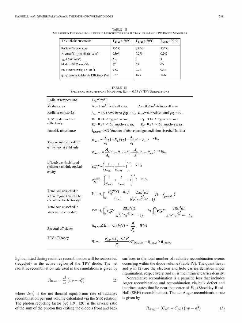
diode in order to recuperate below bandgap radiation [5], [6].Quaternary InGaAsSb alloys were investigated because theycan be grown lattice matched to GaSb substrates for bandgapsas low as 0.5 eV [7]–[11]; to date, however, the materialunderperforms compared to ternary InGaAs TPV diodes. Thispaper summarizes the theory used to predict the practical TPVthermal-to-electric energy conversion efficiency for heat trans-ferred radiatively from a hot-side radiator to a cold-side diodemodule. Our analysis uses measured minority carrier recombi-nation coefficients to determine the intrinsic limits to 0.53-eVInGaAsSb TPV diode power conversion efficiency and as-sesses the electronic material quality and architecture (Table I)required to approach these bounds. Fig. 1 shows the architectureof a typical InGaAsSb n-p junction diode investigated duringthis paper. A TPV module refers to the combination of frontsurface spectral control filter and the TPV diode or an arrayof diodes.
II. TPV EFFICIENCY (ηTPV)
The TPV thermal-to-electric power conversion efficiencyηTPV (Table II) is defined as the electrical power output fromthe TPV module divided by the total thermal power absorbedin the module. The thermal power transferred from the hot(Tradiator) radiator to the cold module (Tdiode) is due to theradiative heat transfer across a vacuum gap. The maximumelectrical power from the TPV diode is the product of theopen-circuit voltage (VOC), the short circuit current (ISC),and the fill factor (FF) [12]. Because photons having energies(E < EG) cannot be converted into electricity, it is convenientto evaluate the overall efficiency as the product of the diodeefficiency ηDiode and the spectral efficiency ηSpectral [1], [3].The term ηDiode quantifies the power conversion efficiency forthe above bandgap (E > EG) thermal radiation absorbed in thediode’s active n-p junction area. The term ηSpectral quantifiesthe ratio of the above bandgap radiation absorbed in the activearea divided by the total thermal radiation absorbed in themodule. The breakdown of these efficiency parameters is givenin Table III. The overall expression for TPV thermal-to-electricpower conversion efficiency ηTPV is
ηTPV = ηSpectral × ηDiode
=VOC × ISC × FF
ATotal
∫ ∞0 εcavityeff
2πE3
h3c2(eE/kTradiator−1)dE(1)
0018-9383/$20.00 © 2006 IEEE
2880 IEEE TRANSACTIONS ON ELECTRON DEVICES, VOL. 53, NO. 12, DECEMBER 2006
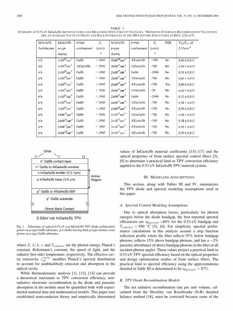
TABLE ISUMMARY OF 0.53-eV InGaAsSb ARCHITECTURES AND MEASURED OPEN-CIRCUIT VOLTAGES. ∗REPORTED INTERFACE RECOMBINATION VELOCITIES
ARE AN AVERAGE VALUE OF FRONT AND BACK INTERFACES IN THE DH LIFETIME STRUCTURES IN REFS. [15]–[17]
Fig. 1. Schematic of typical 0.53-eV n-p InGaAsSb TPV diode architecturesgrown on p-type GaSb substrates. p-n diodes having thick p-type emitters weregrown on n-type GaSb substrates.
where E, h, k, c, and Tradiator are the photon energy, Planck’sconstant, Boltzmann’s constant, the speed of light, and theradiator (hot side) temperature, respectively. The effective cav-ity emissivity εcavityeff modifies Planck’s spectral distributionto account for nonblackbody emission and absorption in theoptical cavity.
While thermodynamic analysis [1], [13], [14] can providea theoretical maximum to TPV conversion efficiency, non-radiative electronic recombination in the diode and parasiticabsorption in the module must be quantified both with experi-mental material data and mathematical models. This paper usesestablished semiconductor theory and empirically determined
values of InGaAsSb material coefficients [15]–[17] and theoptical properties of front surface spectral control filters [5],[6] to determine a practical limit to TPV conversion efficiencyapplied to the 0.53-eV InGaAsSb TPV material system.
III. MODELING ASSUMPTIONS
This section, along with Tables III and IV, summarizesthe TPV diode and spectral modeling assumptions used inthis paper.
A. Spectral Control Modeling Assumptions
Due to optical absorption losses, particularly for photonenergies below the diode bandgap, the best reported spectralefficiencies are ηSpectral ∼80% for the 0.53-eV bandgap andTradiator = 950 C [5], [6]. For simplicity, spectral perfor-mance calculations in this analysis assume a step functionreflection profile where the filter reflects 97% below bandgapphotons, reflects 15% above bandgap photons, and has a ∼2%parasitic absorbance of above bandgap photons in the filter at allincident photon angles. These values project a practical limit to0.53-eV TPV spectral efficiency based on the optical propertiesand design optimization studies of front surface filters. Thepractical limit to spectral efficiency using the approximationsdetailed in Table III is determined to be ηSpectral = 87%.
B. TPV Diode Recombination Models
The net radiative recombination rate per unit volume, cal-culated from the Shockley van Roosbroeke (SvR) detailedbalance method [18], must be corrected because some of the
DASHIELL et al.: QUATERNARY InGaAsSb THERMOPHOTOVOLTAIC DIODES 2881
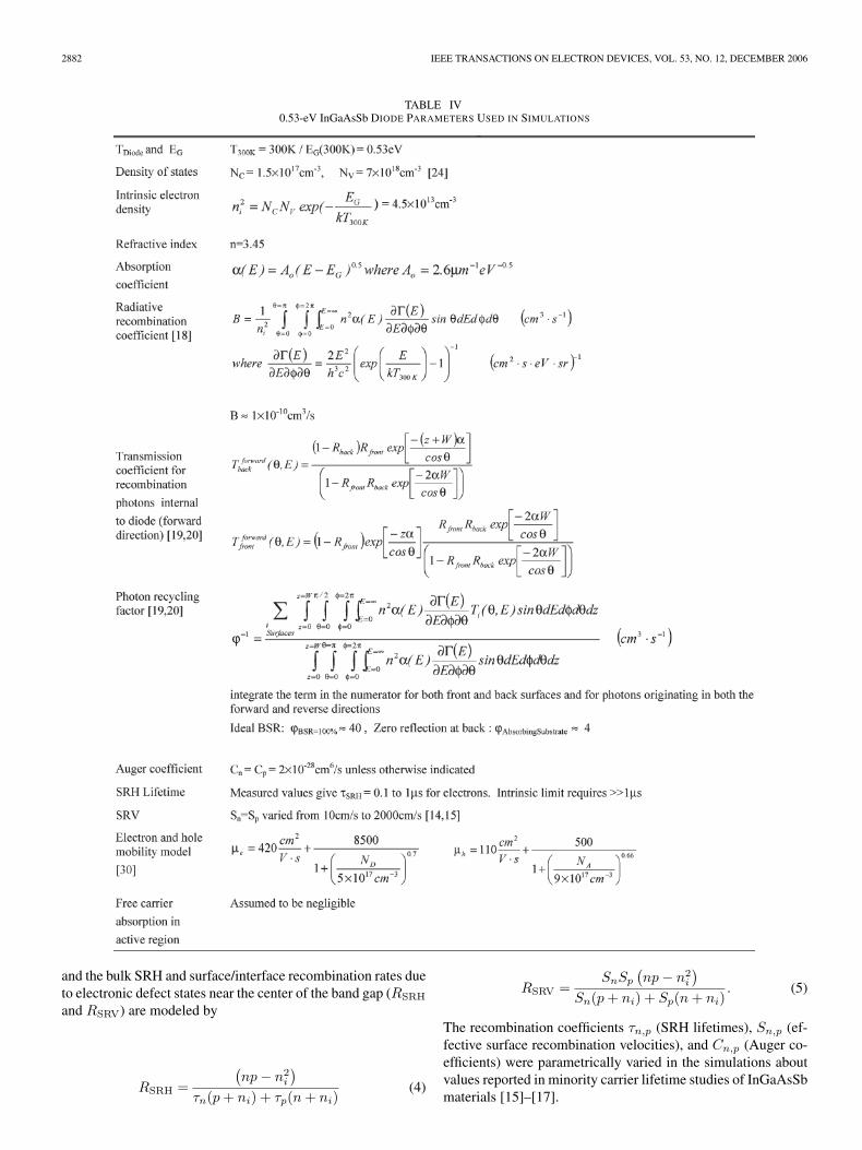
TABLE IIMEASURED THERMAL-TO-ELECTRIC EFFICIENCIES FOR 0.53-eV InGaAsSb TPV DIODE MODULES
TABLE IIISPECTRAL ASSUMPTIONS MADE FOR EG = 0.53 eV TPV PREDICTIONS
light emitted during radiative recombination will be reabsorbed(recycled) in the active region of the TPV diode. The netradiative recombination rate used in the simulations is given by
RRad =B
ϕ
(np − n2i
)(2)
where Bn2i is the net thermal equilibrium rate of radiativerecombination per unit volume calculated via the SvR relation.The photon recycling factor (ϕ) [19], [20] is the inverse ratioof the sum of the photon flux exiting the diode’s front and back
surfaces to the total number of radiative recombination eventsoccurring within the diode volume (Table IV). The quantities nand p in (2) are the electron and hole carrier densities underillumination, respectively, and ni is the intrinsic carrier density.
Nonradiative recombination is a parasitic loss that includesAuger recombination and recombination via bulk defect andinterface states that lie near the center of EG (Shockley-Read-Hall (SRH) recombination). The net Auger recombination rateis given by
RAug = (Cnn + Cpp)(np − n2i
)(3)
2882 IEEE TRANSACTIONS ON ELECTRON DEVICES, VOL. 53, NO. 12, DECEMBER 2006
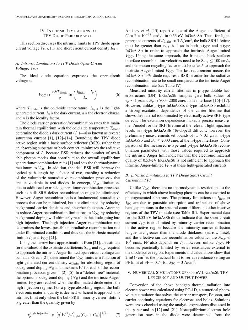
TABLE IV0.53-eV InGaAsSb DIODE PARAMETERS USED IN SIMULATIONS
and the bulk SRH and surface/interface recombination rates dueto electronic defect states near the center of the band gap (RSRH
and RSRV) are modeled by
RSRH =
(np − n2i
)τn(p + ni) + τp(n + ni)
(4)
RSRV =SnSp
(np − n2i
)Sn(p + ni) + Sp(n + ni)
. (5)
The recombination coefficients τn,p (SRH lifetimes), Sn,p (ef-fective surface recombination velocities), and Cn,p (Auger co-efficients) were parametrically varied in the simulations aboutvalues reported in minority carrier lifetime studies of InGaAsSbmaterials [15]–[17].
DASHIELL et al.: QUATERNARY InGaAsSb THERMOPHOTOVOLTAIC DIODES 2883
IV. INTRINSIC LIMITATIONS TO
TPV DIODE PERFORMANCE
This section discusses the intrinsic limits to TPV diode open-circuit voltage VOC, FF, and short circuit current density ISC.
A. Intrinsic Limitations to TPV Diode Open-CircuitVoltage: VOC
The ideal diode equation expresses the open-circuitvoltage as
VOC ≈ nkTdiodeq
ln(
Ilight − Io
Io
)(6)
where Tdiode is the cold-side temperature, Ilight is the light-generated current, I0 is the dark current, q is the electron charge,and n is the ideality factor.
The diode carrier generation/recombination rates that main-tain thermal equilibrium with the cold side temperature Tdiodedetermine the diode’s dark current (I0)—also known as reversesaturation current [1], [12]–[14]. Bounding the TPV diodeactive region with a back surface reflector (BSR), rather thanan absorbing substrate or back contact, minimizes the radiativecomponent of I0 because BSR reduces the number of avail-able photon modes that contribute to the overall equilibriumgeneration/recombination rates [1] and sets the thermodynamicmaximum to VOC. In addition, the ideal BSR will increase theoptical path length by a factor of two, enabling a reductionof the volumetric nonradiative recombination processes thatare unavoidable in real diodes. In concept, VOC limitationsdue to additional extrinsic generation/recombination processessuch as bulk SRH defect recombination might be eliminated.However, Auger recombination is a fundamental nonradiativeprocess that can be minimized, but not eliminated, by reducingbackground carrier densities and absorber thickness. Attemptsto reduce Auger recombination limitations to VOC by reducingbackground doping will ultimately result in the diode going intohigh injection. The high injection Auger recombination ratedetermines the lowest possible nonradiative recombination rateunder illuminated conditions and thus sets the intrinsic materiallimit to I0 and VOC [21].
Using the narrow base approximations from [21], an estimatefor the values of the extrinsic coefficients Sn,p and τn,p requiredto approach the intrinsic Auger-limited open-circuit voltage canbe made. Green [21] determined the VOC limits as a function oflight-generated current density JLight for absorbing region ofbackground doping NB and thickness W for each of the recom-bination processes given in (2)–(5). In a “defect-free” material,the optimum background doping (NB) and the intrinsic Auger-limited VOC are reached when the illuminated diode enters thehigh-injection regime. For a p-type absorbing region, the bulkelectronic material quality is deemed sufficient to approach thisintrinsic limit only when the bulk SRH minority carrier lifetimeis greater than the quantity given by
τhigh injectionp [q2W 2/J2Light(CP + Cn)
]1/3. (7)
Anikeev et al. [15] report values of the Auger coefficient ofC ≈ 2 × 10⁻²⁸ cm6/s in 0.53-eV InGaAsSb. Thus, for light-generated currents of JLight ≈ 3 A/cm2, the bulk SRH lifetimemust be greater than τn,p 1 µs in both n-type and p-typeInGaAsSb in order to approach the intrinsic Auger-limitedVOC. Using the same approach, the front and back surface/interface recombination velocities need to be Sn,p ≤ 100 cm/s,and the photon recycling factor must be ϕ 5 to approach theintrinsic Auger-limited VOC. The last requirement means theInGaAsSb TPV diode requires a BSR in order for the radiativerecombination rate to be small compared to the intrinsic Augerrecombination rate (see Table IV).
Measured minority carrier lifetimes in p-type double het-erostructure (DH) InGaAsSb samples give bulk values ofτp ∼ 1 µs and Sp ≈ 700−2000 cm/s at the interfaces [15]–[17].However, unlike p-type InGaAsSb, n-type InGaAsSb exhibitsa strong excitation dependence of the carrier lifetime thatshows the material is dominated by electrically active SRH-typedefects. The excitation dependence makes a precise measure-ment/model for the SRH lifetime at the relevant light injectionlevels in n-type InGaAsSb (Te-doped) difficult; however, thepreliminary measurements set bounds of τn ≥ 0.1 µs in n-typeInGaAsSb and Sn ≤ 2000 cm/s at the n-type interfaces. Com-parison of the measured n-type and p-type InGaAsSb recom-bination parameters with those values required to approachthe intrinsic Auger limit indicates that the electronic materialquality of 0.53-eV InGaAsSb is not sufficient to approach theintrinsic Auger-limited VOC at these light-generated currents.
B. Intrinsic Limitations to TPV Diode Short CircuitCurrent and FF
Unlike VOC, there are no thermodynamic restrictions to theefficiency in which above bandgap photons can be converted tophotogenerated electrons. The primary limitations to Ilight ≈ISC are due to parasitic absorption and reflections of abovebandgap photons in the spectral control filter and other inactiveregions of the TPV module (see Table III). Experimental datafor the 0.53-eV InGaAsSb diode indicate that the short circuitcurrent ISC is not limited by minority carrier recombinationin the active region because the minority carrier diffusionlengths are greater than the diode thickness (narrow base),and the effective surface recombination velocities are Sn,p <104 cm/s. FF also depends on I0; however, unlike VOC, FFbecomes practically limited by series resistances external tothe diode active region. Experiments and calculations show that2 mΩ · cm2 is the practical limit to series resistance setting anFF limit of FF = 0.74 for JSC = 3 A/cm2.
V. NUMERICAL SIMULATIONS OF 0.53-eV InGaAsSb TPVEFFICIENCY AND OUTPUT POWER
Conversion of the above bandgap thermal radiation intoelectric power was calculated using PC-1D, a numerical photo-voltaic simulator that solves the carrier transport, Poisson, andcarrier continuity equations for electrons and holes. Solutionswere cross checked using the analytic expressions discussed inthis paper and in [12] and [21]. Nonequilibrium electron–holegeneration rates in the diode were determined from the
2884 IEEE TRANSACTIONS ON ELECTRON DEVICES, VOL. 53, NO. 12, DECEMBER 2006
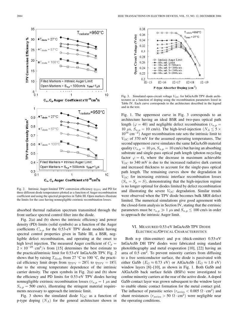
Fig. 2. Intrinsic Auger-limited TPV conversion efficiency ηTPV and PD forthree different diode temperatures plotted as a function of Auger recombinationcoefficient and using the spectral properties in Table III. Open markers illustratethe limits for the case having nonnegligible extrinsic recombination losses.
absorbed thermal radiation spectrum transmitted through thefront surface spectral control filter into the diode.
Fig. 2(a) and (b) shows the intrinsic efficiency and powerdensity (PD) limits (solid symbols) as a function of the Augercoefficients Cn,p for the 0.53-eV TPV diode module havingspectral control properties given in Table III, a BSR, neg-ligible defect recombination, and operating at the onset tohigh level injection. The measured Auger coefficient of Cp =2 × 10⁻²⁸ cm6/s from [15] determines the best estimate tothe practical/intrinsic limit for 0.53-eV InGaAsSb TPV. Fig. 2shows that by raising Tdiode from 27 C to 100 C, the practi-cal efficiency limit drops from ηTPV = 28% to ηTPV = 18%due to the strong temperature dependence of the intrinsiccarrier density. The open symbols in Fig. 2(a) and (b) showthe efficiency and PD limits for 0.53-eV TPV diodes havingnonnegligible extrinsic recombination losses (τn,p = 1 µs andSn,p = 500 cm/s), illustrating the stringent material require-ments necessary to approach the intrinsic limit.
Fig. 3 shows the simulated diode VOC as a function ofp-type doping (NA) for the general architecture shown in
Fig. 3. Simulated open-circuit voltage VOC for InGaAsSb TPV diode archi-tectures as a function of doping using the recombination parameters listed inTable IV. Each curve corresponds to the architecture described in the legendand in the text.
Fig. 1. The uppermost curve in Fig. 3 corresponds to anarchitecture having an ideal BSR and two-pass optical pathlength (ϕ = 40) and negligible defect recombination (τn,p =10 µs, Sn,p = 10 cm/s). The high-level-injection (NA ≤ 5 ×1016 cm−3) Auger recombination rate sets the intrinsic limit toVOC of 370 mV for the assumed operating temperatures. Thesecond uppermost curve simulates the same InGaAsSb materialquality (τn,p = 10 µs, Sn,p = 10 cm/s) but having an absorbingsubstrate and single-pass optical path length (photon recyclingfactor ϕ = 4), where the decrease in maximum achievableVOC to 340 mV is due to the increased radiative dark currentand increased thickness to account for the single-pass opticalpath length. The remaining curves show the degradation inVOC for increasing extrinsic interface recombination losses(Sn = Sp = S), demonstrating that the high-injection regimeis no longer optimal for diodes limited by defect recombinationand illustrating the severe VOC degradation. Similar trendswere observed when the TPV diode becomes bulk SRH defectlimited. The numerical simulations give good agreement withthe closed-form analysis in Section IV, stating that the extrinsicparameters must be τn,p 1 µs and Sn,p ≤ 100 cm/s in orderto approach the intrinsic Auger limit.
VI. MEASURED 0.53-eV InGaAsSb TPV DIODE
ELECTRICAL/OPTICAL CHARACTERISTICS
Both n-p (thin-emitter) and p-n (thick-emitter) 0.53-eVInGaAsSb DH TPV diodes were fabricated using standardphotolithography and metal evaporation [10], [22] having anarea of 0.5 cm2. To prevent minority carriers from diffusingto a free semiconductor surface, the diode is passivated witheither GaSb (EG ≈ 0.73 eV) or AlGaAsSb (EG ≈ 1.0 eV)window layers [8]–[10], as shown in Fig. 1. Both GaSb andAlGaAsSb back surface fields (BSFs) were investigated toconfine minority carriers at the rear of the active diode. A dopedGaSb contact layer was grown subsequent to the window layerto enable ohmic contact formation for the metal contact grid.The influence of parasitic series (rseries < 0.005 Ω · cm2) andshunt resistances (rseries > 50 Ω · cm2) were negligible nearthe operating conditions.
DASHIELL et al.: QUATERNARY InGaAsSb THERMOPHOTOVOLTAIC DIODES 2885
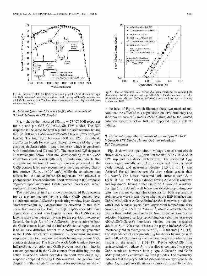
Fig. 4. Measured IQE for 0.53-eV n-p and p-n InGaAsSb diodes having athin GaSb window/contact layer and n-p diode having AlGaAsSb window andthick GaSb contact layer. The inset shows a conceptual band diagram of the twowindow interfaces.
A. Internal Quantum Efficiency (IQE) Measurements of0.53-eV InGaAsSb TPV Diodes
Fig. 4 shows the measured (Tdiode = 27 C) IQE responsesfor n-p and p-n 0.53-eV InGaAsSb TPV diodes. The IQEresponse is the same for both n-p and p-n architectures havingthin (< 200 nm) GaSb window/contact layers (refer to figurelegend). The high IQEs between 1600 and 2250 nm indicatea diffusion length for electrons (holes) in excess of the p-typeabsorber thickness (thin n-type thickness), which is consistentwith simulations and [7] and [10]. The measured IQE degradesat wavelengths below 1600 nm, corresponding to the GaSbabsorption cutoff wavelength [23]. Simulations indicate thata significant fraction of minority carriers generated in theGaSb contact layer may recombine at the unpassivated GaSb-free surface (Ssurface ≈ 105 cm/s) while the remainder maydiffuse into the active InGaAsSb region and be collected asphotocurrent. The experimental short-wavelength IQE responsedegraded upon increasing GaSb contact thicknesses, whichsupports this conclusion.
The third data set in Fig. 4 shows the measured IQE responsefor an n-p architecture having a thick GaSb contact layer(> 400 nm) and an AlGaAsSb passivating window layer. Severeshort-wavelength IQE degradation is observed in this thirdcurve for two reasons. First, the IQE experiences additionaldegradation at short wavelengths because the GaSb contactlayer is more than twice as thick as for the previous two curves.Second, the high EG of the AlGaAsSb layer relative to boththe GaSb contact layer and the InGaAsSb active region causesit to act as a diffusion barrier to minority carriers generatedin the GaSb, which was confirmed by comparing measuredresponses from two window materials having equivalent GaSbcontact thicknesses. The high EG AlGaAsSb window betweenInGaAsSb active region and GaSb prevents nearly all minoritycarriers generated in the GaSb contact from diffusing into theactive InGaAsSb, which degrades the short-wavelength IQEresponse compared to using GaSb windows. The generic banddiagrams in the vicinity of the emitter for n-p diodes are shown
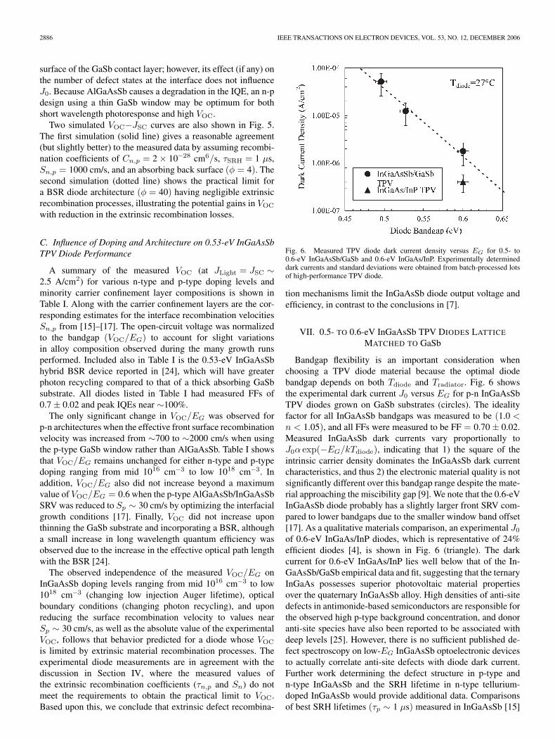
Fig. 5. Plot of measured VOC versus JSC data (markers) for various lightilluminations for 0.53-eV p-n and n-p InGaAsSb TPV diodes. Inset providesinformation on whether GaSb or AlGaAsSb was used for the passivatingwindow and BSF.
in the inset of Fig. 4, which illustrate these two mechanisms.Note that the effect of this degradation on TPV efficiency andshort circuit current is small (<5% relative) due to the limitedradiation spectrum below 1600 nm expected from a 950 Cradiator.
B. Current–Voltage Measurements of n-p and p-n 0.53-eVInGaAsSb TPV Diodes Having GaSb or InGaAsSbDH Confinement
Fig. 5 shows the open-circuit voltage versus short-circuitcurrent density (VOC−JSC) relation for six 0.53-eV InGaAsSbTPV n-p and p-n diode architectures. The measured VOCvaries logarithmically with JSC, as expected from the idealdiode model, and near-unity ideality (1.0 < n < 1.1) wasobserved for all architectures for JSC values greater than0.1 A/cm2. The lowest measured dark currents were Jo =1.5 × 10⁻⁵ A · cm−2 for p-n diodes having AlGaAsSb windowsand n-p diodes having either GaSb or AlGaAsSb windows.For JSC > 0.1 A/cm2, well below our expected operating cur-rents, the current voltage characteristics for both n-p and p-narchitectures were insensitive to whether the BSF interface wasGaSb/InGaAsSb or AlGaAsSb/InGaAsSb. However, p-n diodeswith GaSb window layers have larger room temperature darkcurrents of Jo = 2.5 × 10⁻⁵ A/cm−2, which is attributed to thegreater than twofold increase in the front surface recombinationvelocity. Measured surface recombination velocities at p-typeAlGaAsSb/InGaAsSb interfaces yielded average measuredvalues of Sp ∼ 700 cm/s, whereas the p-type InGaAsSb/GaSbinterfaces yield an average value of Sp ∼ 2000 cm/s [15]–[17].The dependence of experimental J0 for diodes having p-GaSband p-AlGaAsSb minority confinement layers provides furtherinsight on the results in [15]–[17]. P-type AlGaAsSb frontsurface windows reduce J0 in p-n diodes compared to p-typeGaSb windows; however, both p-type AlGaAsSb and GaSbBSFs yield nearly equivalent J0 for n-p diodes. The asymmetryindicates that the p-type AlGaAsSb passivation layer (due to itshigher EG) suppresses the minority carrier diffusion to the free
2886 IEEE TRANSACTIONS ON ELECTRON DEVICES, VOL. 53, NO. 12, DECEMBER 2006
surface of the GaSb contact layer; however, its effect (if any) onthe number of defect states at the interface does not influenceJ0. Because AlGaAsSb causes a degradation in the IQE, an n-pdesign using a thin GaSb window may be optimum for bothshort wavelength photoresponse and high VOC.
Two simulated VOC−JSC curves are also shown in Fig. 5.The first simulation (solid line) gives a reasonable agreement(but slightly better) to the measured data by assuming recombi-nation coefficients of Cn,p = 2 × 10⁻²⁸ cm6/s, τSRH = 1 µs,Sn,p = 1000 cm/s, and an absorbing back surface (φ = 4). Thesecond simulation (dotted line) shows the practical limit fora BSR diode architecture (φ = 40) having negligible extrinsicrecombination processes, illustrating the potential gains in VOCwith reduction in the extrinsic recombination losses.
C. Influence of Doping and Architecture on 0.53-eV InGaAsSbTPV Diode Performance
A summary of the measured VOC (at JLight = JSC ∼2.5 A/cm2) for various n-type and p-type doping levels andminority carrier confinement layer compositions is shown inTable I. Along with the carrier confinement layers are the cor-responding estimates for the interface recombination velocitiesSn,p from [15]–[17]. The open-circuit voltage was normalizedto the bandgap (VOC/EG) to account for slight variationsin alloy composition observed during the many growth runsperformed. Included also in Table I is the 0.53-eV InGaAsSbhybrid BSR device reported in [24], which will have greaterphoton recycling compared to that of a thick absorbing GaSbsubstrate. All diodes listed in Table I had measured FFs of0.7 ± 0.02 and peak IQEs near ∼100%.
The only significant change in VOC/EG was observed forp-n architectures when the effective front surface recombinationvelocity was increased from ∼700 to ∼2000 cm/s when usingthe p-type GaSb window rather than AlGaAsSb. Table I showsthat VOC/EG remains unchanged for either n-type and p-typedoping ranging from mid 1016 cm−3 to low 1018 cm−3. Inaddition, VOC/EG also did not increase beyond a maximumvalue of VOC/EG = 0.6 when the p-type AlGaAsSb/InGaAsSbSRV was reduced to Sp ∼ 30 cm/s by optimizing the interfacialgrowth conditions [17]. Finally, VOC did not increase uponthinning the GaSb substrate and incorporating a BSR, althougha small increase in long wavelength quantum efficiency wasobserved due to the increase in the effective optical path lengthwith the BSR [24].
The observed independence of the measured VOC/EG onInGaAsSb doping levels ranging from mid 1016 cm−3 to low1018 cm−3 (changing low injection Auger lifetime), opticalboundary conditions (changing photon recycling), and uponreducing the surface recombination velocity to values nearSp ∼ 30 cm/s, as well as the absolute value of the experimentalVOC, follows that behavior predicted for a diode whose VOCis limited by extrinsic material recombination processes. Theexperimental diode measurements are in agreement with thediscussion in Section IV, where the measured values ofthe extrinsic recombination coefficients (τn,p and Sn) do notmeet the requirements to obtain the practical limit to VOC.Based upon this, we conclude that extrinsic defect recombina-
Fig. 6. Measured TPV diode dark current density versus EG for 0.5- to0.6-eV InGaAsSb/GaSb and 0.6-eV InGaAs/InP. Experimentally determineddark currents and standard deviations were obtained from batch-processed lotsof high-performance TPV diode.
tion mechanisms limit the InGaAsSb diode output voltage andefficiency, in contrast to the conclusions in [7].
VII. 0.5- TO 0.6-eV InGaAsSb TPV DIODES LATTICE
MATCHED TO GaSb
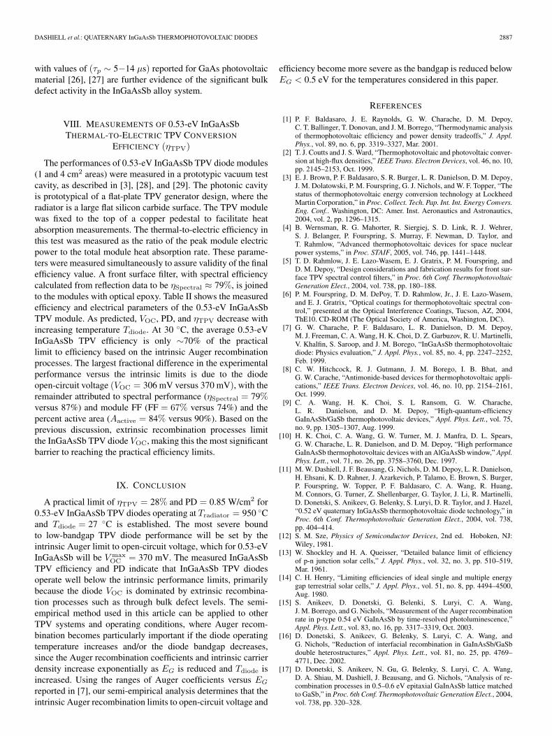
Bandgap flexibility is an important consideration whenchoosing a TPV diode material because the optimal diodebandgap depends on both Tdiode and Tradiator. Fig. 6 showsthe experimental dark current J0 versus EG for p-n InGaAsSbTPV diodes grown on GaSb substrates (circles). The idealityfactor for all InGaAsSb bandgaps was measured to be (1.0 <n < 1.05), and all FFs were measured to be FF = 0.70 ± 0.02.Measured InGaAsSb dark currents vary proportionally toJ0α exp(−EG/kTdiode), indicating that 1) the square of theintrinsic carrier density dominates the InGaAsSb dark currentcharacteristics, and thus 2) the electronic material quality is notsignificantly different over this bandgap range despite the mate-rial approaching the miscibility gap [9]. We note that the 0.6-eVInGaAsSb diode probably has a slightly larger front SRV com-pared to lower bandgaps due to the smaller window band offset[17]. As a qualitative materials comparison, an experimental J0of 0.6-eV InGaAs/InP diodes, which is representative of 24%efficient diodes [4], is shown in Fig. 6 (triangle). The darkcurrent for 0.6-eV InGaAs/InP lies well below that of the In-GaAsSb/GaSb empirical data and fit, suggesting that the ternaryInGaAs possesses superior photovoltaic material propertiesover the quaternary InGaAsSb alloy. High densities of anti-sitedefects in antimonide-based semiconductors are responsible forthe observed high p-type background concentration, and donoranti-site species have also been reported to be associated withdeep levels [25]. However, there is no sufficient published de-fect spectroscopy on low-EG InGaAsSb optoelectronic devicesto actually correlate anti-site defects with diode dark current.Further work determining the defect structure in p-type andn-type InGaAsSb and the SRH lifetime in n-type tellurium-doped InGaAsSb would provide additional data. Comparisonsof best SRH lifetimes (τp ∼ 1 µs) measured in InGaAsSb [15]
DASHIELL et al.: QUATERNARY InGaAsSb THERMOPHOTOVOLTAIC DIODES 2887
with values of (τp ∼ 5−14 µs) reported for GaAs photovoltaicmaterial [26], [27] are further evidence of the significant bulkdefect activity in the InGaAsSb alloy system.
VIII. MEASUREMENTS OF 0.53-eV InGaAsSbTHERMAL-TO-ELECTRIC TPV CONVERSION
EFFICIENCY (ηTPV)
The performances of 0.53-eV InGaAsSb TPV diode modules(1 and 4 cm2 areas) were measured in a prototypic vacuum testcavity, as described in [3], [28], and [29]. The photonic cavityis prototypical of a flat-plate TPV generator design, where theradiator is a large flat silicon carbide surface. The TPV modulewas fixed to the top of a copper pedestal to facilitate heatabsorption measurements. The thermal-to-electric efficiency inthis test was measured as the ratio of the peak module electricpower to the total module heat absorption rate. These parame-ters were measured simultaneously to assure validity of the finalefficiency value. A front surface filter, with spectral efficiencycalculated from reflection data to be ηSpectral ≈ 79%, is joinedto the modules with optical epoxy. Table II shows the measuredefficiency and electrical parameters of the 0.53-eV InGaAsSbTPV module. As predicted, VOC, PD, and ηTPV decrease withincreasing temperature Tdiode. At 30 C, the average 0.53-eVInGaAsSb TPV efficiency is only ∼70% of the practicallimit to efficiency based on the intrinsic Auger recombinationprocesses. The largest fractional difference in the experimentalperformance versus the intrinsic limits is due to the diodeopen-circuit voltage (VOC = 306 mV versus 370 mV), with theremainder attributed to spectral performance (ηSpectral = 79%versus 87%) and module FF (FF = 67% versus 74%) and thepercent active area (Aactive = 84% versus 90%). Based on theprevious discussion, extrinsic recombination processes limitthe InGaAsSb TPV diode VOC, making this the most significantbarrier to reaching the practical efficiency limits.
IX. CONCLUSION
A practical limit of ηTPV = 28% and PD = 0.85 W/cm2 for0.53-eV InGaAsSb TPV diodes operating at Tradiator = 950 Cand Tdiode = 27 C is established. The most severe boundto low-bandgap TPV diode performance will be set by theintrinsic Auger limit to open-circuit voltage, which for 0.53-eVInGaAsSb will be V max
OC = 370 mV. The measured InGaAsSbTPV efficiency and PD indicate that InGaAsSb TPV diodesoperate well below the intrinsic performance limits, primarilybecause the diode VOC is dominated by extrinsic recombina-tion processes such as through bulk defect levels. The semi-empirical method used in this article can be applied to otherTPV systems and operating conditions, where Auger recom-bination becomes particularly important if the diode operatingtemperature increases and/or the diode bandgap decreases,since the Auger recombination coefficients and intrinsic carrierdensity increase exponentially as EG is reduced and Tdiode isincreased. Using the ranges of Auger coefficients versus EG
reported in [7], our semi-empirical analysis determines that theintrinsic Auger recombination limits to open-circuit voltage and
efficiency become more severe as the bandgap is reduced belowEG < 0.5 eV for the temperatures considered in this paper.
REFERENCES
[1] P. F. Baldasaro, J. E. Raynolds, G. W. Charache, D. M. Depoy,C. T. Ballinger, T. Donovan, and J. M. Borrego, “Thermodynamic analysisof thermophotovoltaic efficiency and power density tradeoffs,” J. Appl.Phys., vol. 89, no. 6, pp. 3319–3327, Mar. 2001.
[2] T. J. Coutts and J. S. Ward, “Thermophotovoltaic and photovoltaic conver-sion at high-flux densities,” IEEE Trans. Electron Devices, vol. 46, no. 10,pp. 2145–2153, Oct. 1999.
[3] E. J. Brown, P. F. Baldasaro, S. R. Burger, L. R. Danielson, D. M. Depoy,J. M. Dolatowski, P. M. Fourspring, G. J. Nichols, and W. F. Topper, “Thestatus of thermophotovoltaic energy conversion technology at LockheedMartin Corporation,” in Proc. Collect. Tech. Pap. Int. Int. Energy Convers.Eng. Conf.. Washington, DC: Amer. Inst. Aeronautics and Astronautics,2004, vol. 2, pp. 1296–1315.
[4] B. Wernsman, R. G. Mahorter, R. Siergiej, S. D. Link, R. J. Wehrer,S. J. Belanger, P. Fourspring, S. Murray, F. Newman, D. Taylor, andT. Rahmlow, “Advanced thermophotovoltaic devices for space nuclearpower systems,” in Proc. STAIF, 2005, vol. 746, pp. 1441–1448.
[5] T. D. Rahmlow, J. E. Lazo-Wasem, E. J. Gratrix, P. M. Fourspring, andD. M. Depoy, “Design considerations and fabrication results for front sur-face TPV spectral control filters,” in Proc. 6th Conf. ThermophotovoltaicGeneration Elect., 2004, vol. 738, pp. 180–188.
[6] P. M. Fourspring, D. M. DePoy, T. D. Rahmlow, Jr., J. E. Lazo-Wasem,and E. J. Gratrix, “Optical coatings for thermophotovoltaic spectral con-trol,” presented at the Optical Interference Coatings, Tucson, AZ, 2004,ThE10. CD-ROM (The Optical Society of America, Washington, DC).
[7] G. W. Charache, P. F. Baldasaro, L. R. Danielson, D. M. Depoy,M. J. Freeman, C. A. Wang, H. K. Choi, D. Z. Garbuzov, R. U. Martinelli,V. Khalfin, S. Saroop, and J. M. Borego, “InGaAsSb thermophotovoltaicdiode: Physics evaluation,” J. Appl. Phys., vol. 85, no. 4, pp. 2247–2252,Feb. 1999.
[8] C. W. Hitchcock, R. J. Gutmann, J. M. Borego, I. B. Bhat, andG. W. Carache, “Antimonide-based devices for thermophotovoltaic appli-cations,” IEEE Trans. Electron Devices, vol. 46, no. 10, pp. 2154–2161,Oct. 1999.
[9] C. A. Wang, H. K. Choi, S. L Ransom, G. W. Charache,L. R. Danielson, and D. M. Depoy, “High-quantum-efficiencyGaInAsSb/GaSb thermophotovoltaic devices,” Appl. Phys. Lett., vol. 75,no. 9, pp. 1305–1307, Aug. 1999.
[10] H. K. Choi, C. A. Wang, G. W. Turner, M. J. Manfra, D. L. Spears,G. W. Charache, L. R. Danielson, and D. M. Depoy, “High performanceGaInAsSb thermophotovoltaic devices with an AlGaAsSb window,” Appl.Phys. Lett., vol. 71, no. 26, pp. 3758–3760, Dec. 1997.
[11] M. W. Dashiell, J. F. Beausang, G. Nichols, D. M. Depoy, L. R. Danielson,H. Ehsani, K. D. Rahner, J. Azarkevich, P. Talamo, E. Brown, S. Burger,P. Fourspring, W. Topper, P. F. Baldasaro, C. A. Wang, R. Huang,M. Connors, G. Turner, Z. Shellenbarger, G. Taylor, J. Li, R. Martinelli,D. Donetski, S. Anikeev, G. Belenky, S. Luryi, D. R. Taylor, and J. Hazel,“0.52 eV quaternary InGaAsSb thermophotovoltaic diode technology,” inProc. 6th Conf. Thermophotovoltaic Generation Elect., 2004, vol. 738,pp. 404–414.
[12] S. M. Sze, Physics of Semiconductor Devices, 2nd ed. Hoboken, NJ:Wiley, 1981.
[13] W. Shockley and H. A. Queisser, “Detailed balance limit of efficiencyof p-n junction solar cells,” J. Appl. Phys., vol. 32, no. 3, pp. 510–519,Mar. 1961.
[14] C. H. Henry, “Limiting efficiencies of ideal single and multiple energygap terrestrial solar cells,” J. Appl. Phys., vol. 51, no. 8, pp. 4494–4500,Aug. 1980.
[15] S. Anikeev, D. Donetski, G. Belenki, S. Luryi, C. A. Wang,J. M. Borrego, and G. Nichols, “Measurement of the Auger recombinationrate in p-type 0.54 eV GaInAsSb by time-resolved photoluminescence,”Appl. Phys. Lett., vol. 83, no. 16, pp. 3317–3319, Oct. 2003.
[16] D. Donetski, S. Anikeev, G. Belenky, S. Luryi, C. A. Wang, andG. Nichols, “Reduction of interfacial recombination in GaInAsSb/GaSbdouble heterostructures,” Appl. Phys. Lett., vol. 81, no. 25, pp. 4769–4771, Dec. 2002.
[17] D. Donetski, S. Anikeev, N. Gu, G. Belenky, S. Luryi, C. A. Wang,D. A. Shiau, M. Dashiell, J. Beausang, and G. Nichols, “Analysis of re-combination processes in 0.5–0.6 eV epitaxial GaInAsSb lattice matchedto GaSb,” in Proc. 6th Conf. Thermophotovoltaic Generation Elect., 2004,vol. 738, pp. 320–328.

2888 IEEE TRANSACTIONS ON ELECTRON DEVICES, VOL. 53, NO. 12, DECEMBER 2006
[18] W. van Roosbroeke and W. Shockley, “Photon-radiative recombination ofelectrons and holes in germanium,” Phys. Rev., vol. 94, no. 6, pp. 1558–1560, Jun. 1954.
[19] P. Asbeck, “Self-absorption effects on the radiative lifetime inGaAs–GaAlAs double heterostructures,” J. Appl. Phys., vol. 48, no. 2,pp. 820–822, Feb. 1977.
[20] A. Marti, J. L. Balenzategui, and R. F. Reyna, “Photon recycling andSchockley’s diode equation,” J. Appl. Phys., vol. 82, no. 8, pp. 4067–4075,Oct. 1997.
[21] M. A. Green, “Limits on the open-circuit voltage and efficiency of siliconsolar cells imposed by intrinsic Auger processes,” IEEE Trans. ElectronDevices, vol. ED-31, no. 5, pp. 671–678, May 1984.
[22] R. Huang, C. A. Wang, C. T. Harris, M. K. Connors, and D. A. Shiau,“Ohmic contacts to n-type GaSb and n-type GaInAsSb,” J. Electron.Mater., vol. 33, no. 11, pp. 1406–1410, 2004.
[23] S. J. Adachi, “Optical dispersion relations for GaP, GaAs, GaSb, InP,InAs, InSb, AlGaAs, and InGaAsP,” J. Appl. Phys., vol. 66, no. 12,pp. 6030–6040, Dec. 1989.
[24] R. K. Huang, C. A. Huang, M. K. Connors, and G. W. Turner,“Hybrid back surface reflector GaInAsSb thermophotovoltaic devices,”in Proc. 6th Conf. Thermophotovoltaic Generation Elect., 2004, vol. 738,pp. 329–336.
[25] A. G. Milnes and A. Y. Polyakov, “Review: Gallium antimonide devicerelated properties,” Solid State Electron., vol. 36, no. 6, pp. 803–818,Jun. 1993.
[26] J. M. Olsen, R. K. Ahrenkiel, D. J. Dunlavy, B. Keyes, and A. E. Kibbler,“Ultralow recombination velocity at GaInP/GaAs heterointerfaces,” Appl.Phys. Lett., vol. 55, no. 12, pp. 1208–1210, Sep. 1989.
[27] L. W. Molenkamp, G. L. M. Kampschoer, W. deLange, J. W. F. M. Maes,and P. J. Roksnoer, “Ultralong minority-carrier lifetimes in GaAs grownby low-pressure organometallic vapor-phase epitaxy,” Appl. Phys. Lett.,vol. 54, no. 20, pp. 1992–1994, May 1989.
[28] C. K. Gethers, C. T. Ballinger, and D. M. DePoy, “Thermophotovoltaicefficiency testing,” in Proc. 4th Conf. Thermophotovoltaic GenerationElect., 1998, vol. 460, pp. 335–348.
[29] B. Wernsman, R. R. Siergiej, S. D. Link, R. G. Mahorter,M. N. Palmisiano, R. J. Wehrer, R. W. Shultz, R. L. Messham, S. Murray,C. S. Murray, F. Newman, D. Taylor, D. Depoy, and T. Rahmlow, “Greaterthan 20% radiant heat conversion efficiency of a thermophotovoltaicradiator/module system using reflective spectral control,” IEEE Trans.Electron Devices, vol. 51, no. 3, pp. 512–516, Mar. 2004.
[30] C. A. Wang, H. K. Choi, D. C. Oakley, and G. W. Charache, “Expressionsfit from mobility data of InGaAsSb layers grown on insulating GaAssubstrates given in C.A.,” J. Cryst. Growth, vol. 195, no. 1–4, p. 346,1998.
Michael W. Dashiell was born in Baltimore, MD,in 1970. He received the B.S., M.S., and Ph.D.degrees from the University of Delaware, Newark,in 1992, 1998, and 2001, respectively, all in electricalengineering.
From 1992 to 1996, he was a Research Engineerwith AstroPower Inc. (currently GE Solar), wherehe developed high-efficiency silicon and GaAs solarphotovoltaics. From 1997 to 2002, he was with theDepartment of Electrical Engineering, University ofDelaware, and the Max-Planck-Institute for Solid
State Physics, Stuttgart, Germany, where he conducted research regardingepitaxial growth, electrical and optical characterization of metastable siliconand silicon-carbide-based alloys, tunnel diodes, and self-assembled quantumdots. Since 2002, he has been an Electrical Engineer with the Knolls AtomicPower Laboratory, Niskayuna, NY (operated by Lockheed Martin Corporation,Schenectady, NY, for the U.S. Government), where he has been developing low-bandgap III–V thermophotovoltaic energy converters and high-performancepower electronic motor drives. He is also an Adjunct Professor with UnionGraduate College, Schenectady, and has authored or coauthored over 45 tech-nical publications.
John F. Beausang was born in Hershey, PA, onNovember 11, 1976. He received the B.S. degree inengineering science from Pennsylvania State Univer-sity, University Park, in 1999 and the M.S. degree inphysics from Rensselaer Polytechnic Institute, Troy,NY, in 2002. He is currently working toward thePh.D. degree in physics at the University of Penn-sylvania, Philadelphia.
Until 2004, he was with Lockheed Martin Cor-poration, Schenectady, NY, where he worked onthermophotovoltaic technology.
Hassan Ehsani received the B.S. and M.S. degreesin physics from the University of Tehran, Tehran,Iran, in 1974 and 1976, respectively, the M.S. degreefrom The University of Kansas, Lawrence, in 1984,and the Ph.D. degree from The University of Texas,Austin, both in electrical engineering, in 1988.
From 1976 to 1981, he was a faculty member withthe University of Tehran. From 1988 to 2000, he wasa Research Scientist with Rensselaer PolytechnicInstitute, Troy, NY. Since 2000, he has been a Se-nior Scientist with Knolls Atomic Power Laboratory,
Niskayuna, NY (operated by Lockheed Martin Corporation, Schenectady, NY,for the U.S. Government). His research interests have covered a wide range ofsemiconductor physics and optoelectronic materials including organometallicchemical vapor deposition (OMCVD) growth of II–VI and III–V based com-pound semiconductors for infrared detectors, lasers, and thermophotovoltaics;metallization of group II–VI and III–V semiconductors, thermophotovoltaics,and solar cell devices; and processing, characterizations, and modeling. He isthe author or coauthor of over 80 technical publications.
G. J. Nichols, photograph and biography not available at the time ofpublication.
David M. Depoy received the B.S. and M.S.degrees from Rensselaer Polytechnic Institute, Troy,NY, in 1989 and 1993, respectively, both in mechan-ical engineering.
Since 1989, he has been with the AdvancedConcepts Group, Knolls Atomic Power Labora-tory, Niskayuna, NY (operated by Lockheed MartinCorporation, Schenectady, NY, for the U.S. Gov-ernment), investigating direct energy conversiontechnologies. He has worked in the field of ther-mophotovoltaic (TPV) energy conversion for the past
13 years with emphasis on spectral control, characterization, performance mod-eling, and generator design. He is the author or coauthor of over 30 technicalpublications and holds five U.S. patents.
Lee R. Danielson received the B.S. degree fromIowa State University, Ames, in 1968, the M.S.degree from the University of Washington, Seattle,in 1969, and the Ph.D. degree from Washington StateUniversity, in 1977, all in physics.
From 1979 to 1988, he was with Thermo ElectronCorporation, Waltham, MA, where he performedresearch on higher efficiency thermionic and ther-moelectric energy conversion. Since 1989, he hasbeen with Lockheed Martin Corporation, Schenec-tady, NY, where he has worked on thermoelectric and
thermophotovoltaic energy conversion and has developed several electrical andthermal property measurement systems.
DASHIELL et al.: QUATERNARY InGaAsSb THERMOPHOTOVOLTAIC DIODES 2889
Phil Talamo received the B.S. degree in marine en-gineering systems from the United States MerchantMarine Academy, Kings Point, NY, in 1984.
In 1984, he joined Knolls Atomic Power Labora-tory, Niskayuna, NY (operated by Lockheed MartinCorporation, Schenectady, NY, for the U.S. Gov-ernment), where he is currently managing a groupconducting research and development of advancedenergy conversion technologies, specifically directenergy conversion. The bulk of the research effortis on thermophotovoltaics (TPV) with efforts to
improve the conversion efficiency of high-performance semiconductor TPVdevices and filters. His career started as an Operational Engineer at one ofthe nation’s naval nuclear operating prototype, where naval personnel learn thefundamentals of operation prior to being assigned to one of the nation’s nuclear-powered submarine or aircraft carrier. Prior to his current position, he managedthe training program at the nuclear prototype, responsible for the training of allnavy sailors.
Kevin D. Rahner received the B.S. degree in physicsfrom the University at Albany, State University ofNew York (SUNY), Albany, and the M.S. degree inelectrical engineering from Binghamton University,SUNY.
Since 2002, he has been an Engineer with Lock-heed Martin Corporation, Schenectady, NY, workingon electrical performance modeling and radiativeheat transfer modeling of TPV systems.
Edward J. Brown received the B.S. degree inphysics and the M.S. degree in physics from the StateUniversity of New York at New Paltz in 1979 and theM.S. degree in nuclear engineering from RensselaerPolytechnic Institute, Troy, NY, in 1983.
In 1982, he joined the technical staff with KnollsAtomic Power Laboratory, Niskayuna, NY (operatedby Lockheed Martin Corporation, Schenectady, NY,for the U.S. Government), working in the areas ofreactor core design, reactor safety analysis, and ex-perimental reactor operations. In 1990, he joined the
Advanced Concepts Group working on direct energy conversion. Since 1997,he has supervised the energy conversion testing program supporting the de-velopment of thermophotovoltaic energy conversion technology. He holds fourU.S. patents. His areas of research interest include direct energy conversion,nuclear reactor core design, and reactor dynamics modeling.
Mr. Brown is a member of Tau Beta Pi and Alpha Nu Sigma and was thePresident of the NENY Section of the American Nuclear Society.
Steven R. Burger received the B.S. degree in chem-ical engineering from Manhattan College, Riverdale,NY, in 1986 and the M.S. degree in mechanicalengineering from Union College, Schenectady, NY,in 1986.
Since 1982, he has been with the Knolls AtomicPower Laboratory, Niskayuna, NY (operated byLockheed Martin Corporation, Schenectady, for theU.S. Government), where he is currently a SeniorEngineer in the Advanced Components and SystemsUnit working on turbomachinery design. He is the
author or coauthor of ten technical publications. His development and workinterests have covered a wide range of engineering disciplines includingsemiconductor packaging development for direct energy conversion devices,nondestructive test development for reactor plant components, reactor plantfluid system design, and reactor plant equipment maintenance and modification.
Patrick M. Fourspring received the B.S. and M.S.degrees in structural mechanics from Clemson Uni-versity, Clemson, SC, in 1982 and 1986, respectively,and the Ph.D. degree in engineering science andmechanics from the Pennsylvania State University,University Park, in 1997.
His entire career has been associated with nuclearpower. From 1980 to 1990, he was with Duke Power(now Duke Energy), where he was a CooperativeEducation Student supporting system modificationsfor operating nuclear power stations and a Design
Engineer responsible for the identification and implementation of technologyto improve the performance of nuclear power stations. In 1994, he joinedthe Knolls Atomic Power Laboratory, Niskayuna, NY (operated by LockheedMartin Corporation, Schenectady, NY, for the U.S. Government) and hascompleted numerous mechanical analyses of the nuclear reactor componentsas well as assessments of various nuclear reactor configurations. Since 2003,he has been leading the development of spectral control technology for ther-mophotovoltaic energy conversion of heat from a nuclear reactor source.
Dr. Fourspring is a member of the American Society of Mechanical Engi-neers (ASME). He is a Registered Professional Engineer.
William F. Topper, Jr. received the B.S. degreein mechanical engineering from Cornell University,Ithaca, NY, in 1971, and the M.S. degree in me-chanical engineering from Rensselaer PolytechnicInstitute, Troy, NY, in 1974. He is currently workingtoward the Ph.D. degree at Rensselaer PolytechnicInstitute.
He has 35 years of professional experience cov-ering developmental testing of gas turbine enginecomponents with AVCO Lycoming; program man-agement for manufacturing, development, and de-
sign of nuclear system components with General Electric; and design andprofessional engineering certification of medical waste incinerator and en-ergy recovery systems with WFT Engineering Services. He is currently withLockheed Martin Corporation, Schenectady, NY, and has been in severalpositions providing technical customer support, performing component design,and working on development and testing of nuclear power plant equipment.His current position involves the development of energy conversion systemsand components and the design and operation of developmental test apparatusfor advanced mass transport system components.
P. F. Baldasaro, photograph and biography not available at the time ofpublication.
Christine A. Wang received the S.B., M.S., andPh.D. degrees from the Materials Science and En-gineering Department, Massachusetts Institute ofTechnology, Lexington, in 1977, 1978, and 1984,respectively.
In 1984, she joined Lincoln Laboratory, Massa-chusetts Institute of Technology, Cambridge, whereshe is currently a Senior Staff Member in the Electro-Optical Materials and Devices Group and workson III–V materials grown by organometallic vaporphase epitaxy (OMVPE) for advanced optoelectronic
devices. She is the author or coauthor of over 140 technical publications andholds four U.S. patents. Her research interests include gas transport and designof OMVPE reactors, growth and materials characterization of diode lasers,thermophotovoltaic devices, and detectors.
Dr. Wang is a member of Tau Beta Pi, Sigma Xi, and the Materials ResearchSociety. She is currently the Vice-President of the American Association ofCrystal Growth.
2890 IEEE TRANSACTIONS ON ELECTRON DEVICES, VOL. 53, NO. 12, DECEMBER 2006
Robin K. Huang (M’03) received the S.B. degree inphysics with electrical engineering from the Massa-chusetts Institute of Technology (MIT), Cambridge,in 1995, and the M.S. degree in electrical engineer-ing and the Ph.D. degree in applied physics fromStanford University, Stanford, CA, in 1997 and 2000,respectively. In 2000, he joined Lincoln Laboratory,MIT, where he is currently a Staff Member. He isthe author or coauthor of over 35 technical publi-cations. His research interests include high-powernear-infrared semiconductor diode lasers, ther-
mophotovoltaic devices, mid-IR diode lasers, and vertical cavity surface emit-ting lasers (VCSELs).
Michael K. Connors received the B.S. degree inbiological science and environmental science fromthe University of Massachusetts, Lowell, in 1977.
In 1977, he joined Lincoln Laboratory, Massa-chusetts Institute of Technology, Cambridge, wherehe is currently an Assistant Staff Member in theElectro-Optical Materials and Devices Group. He isthe coauthor of over 45 publications. His researchinterests include development of device fabricationprocesses, reactive ion etching of semiconductormaterials, and thin-film deposition of dielectric andmetal coatings.
George W. Turner (M’00) received the B.S., M.S.,and Ph.D. degrees in electrical engineering fromJohns Hopkins University, Baltimore, MD, in 1972,1975, and 1979, respectively.
In 1979, he joined Lincoln Laboratory, Massa-chusetts Institute of Technology, Cambridge, wherehe has been a Staff Member in a number of differentgroups in the Solid-State Division. He is currently anAssistant Leader in the Electro-Optical Materials andDevices Group. He authored or coauthored severalbook chapters, over 125 technical publications, and
holds four U.S. patents. His research interests have covered a wide range ofdevice fabrication and material growth areas, including avalanche photodiodes,direct energy conversion devices, and mid-infrared lasers.
Zane A. Shellenbarger received the M.S.E.E. degree from the University ofDelaware, Newark, and the B.A. degree in physics from Cornell University,Ithaca, NY.
He was with AstroPower Inc. and Structured Materials Inc. for 11 years,working on the development of epitaxial growth and the fabrication of ther-mophotovoltaics, solar cells, infrared detectors, and LEDs. In 2000, he joinedSarnoff Corporation, Princeton, NJ, where he is currently a Member of Tech-nical Staff and has been responsible for the epitaxial growth of InP-, GaAs-,and GaSb-based lasers, thermophotovoltaic cells, and other optoelectronicdevices. He is the author of over 40 technical publications in journals andconference proceedings on laser diodes, photovoltaics, thermophotovoltaics,infrared detectors, and other optoelectronic devices. His technical expertise isin the epitaxial growth of semiconductor materials by metalorganic chemicalvapor deposition and the characterization of semiconductor materials.
Gordon Taylor (S’76–M’76) received the B.S., M.S., and Ph.D. degrees inelectrical engineering (solid state device specialization) from Rutgers Univer-sity, Camden, NJ, in 1969, 1972, and 1976, respectively.
He has been with Sarnoff Corporation, Princeton, NJ, for over 30 years.
Jizhong Li received the M.S. degree in optoelectronics and information en-gineering from Shandong University, Qingdao, China, in 1989 and the Ph.D.degree in solid-state physics from Kansas State University, Manhattan, in 1999.
Before 1994, he was an Associate Professor with the Department of Physics,Qufu Normal University, Qufu, China, where he conducted research on laserbeam modulation and polarization technologies. During his postdoctoral re-search with North Carolina State University in 2000, he conducted AlGaN/GaNmaterial growths by metal organic chemical vapor deposition (MOCVD) forthe fabrication of solar blind (250–280 nm) detector arrays. From 2000 to2005, he was a member of Technical Staff with Sarnoff Corporation, wherehe conducted the development of various III–V compound materials for fab-ricating high power lasers and thermophotovoltaic devices. He is currently aResearch Scientist with the Center for Optical Technologies, Lehigh University,Bethlehem, PA.
Ramon Martinelli (S’59–M’84) received the A.B. and M.S. degrees in elec-trical engineering from Dartmouth College, Hanover, NH, in 1960 and 1961,respectively, and the Ph.D. degree in electrical engineering from PrincetonUniversity, Princeton, NJ, in 1965.
He is a Distinguished Member of Technical Staff with Sarnoff Corporation,Princeton, NJ.
Dmitry Donetski (SM’98–M’97) received theDiploma (with Honors) and the Ph.D. degree inphysics from St. Petersburg State Technical Univer-sity, St. Petersburg, Russia, in 1987 and 1996, respec-tively, and the Ph.D. degree in electrical engineeringfrom the State University of New York, Stony Brook,in 2000.
From 1987 to 1996, he was with the Departmentof Semiconductor Physics and Nanoelectronics, St.Petersburg State Technical University, working onthe design of far-infrared semiconductor lasers and
electrooptic modulators on hot carriers. In 1996, he joined the OptoelectronicsGroup, Electronics and Communications Engineering Department, State Uni-versity of New York, Stony Brook. His research is focused on the design andtechnology of optoelectronic devices including thermophotovoltaic cells, mid-infrared laser diodes, and laser diode arrays. He has 50 publications in referredjournals and conference proceedings.
Sergei Anikeev received the M.Sc. degree (withthe MSU Graduation medal) in physics fromLomonosov Moscow State University (MSU),Moscow, Russia, in 2000, and the Ph.D. degree inelectrical engineering from State University of NewYork, Stony Brook, in 2006.
In 1998, he was awarded the scholarship ofTeaching-Research Center “Fundamental Optics andSpectroscopy.” He is currently with the State Uni-versity of New York. He authored or coauthored15 papers in scientific journals and conference pro-
ceedings. His research interests include experimental and analytical study ofenergy relaxation processes in semiconductors and physics of thermophoto-voltaic devices.
DASHIELL et al.: QUATERNARY InGaAsSb THERMOPHOTOVOLTAIC DIODES 2891
Gregory L. Belenky (M’95–SM’96–F’05) receivedthe Doctor of Physics and Mathematics degree inRussia.
In 1991, he was with AT&T Bell Labs,Murray Hill, NJ. In 1995, he joined the State Univer-sity of New York, Stony Brook, where he is currentlya Professor in the Department of Electrical and Com-puter Engineering. He has published over 140 papersand four reviews and filed four U.S. patents dealingwith the physics of two-dimensional structures andphysics and design of photonic devices. His current
interests include physics of semiconductors and the design and working perfor-mance of semiconductor lasers and optoelectronic systems.
Serge Luryi (M’81–SM’85–F’89) received thePh.D. degree in physics from the University ofToronto, Ontario, Canada, in 1978. His doctoral the-sis was on the theoretical studies of intermolecularinteractions in solid hydrogen.
In 1980, he was with Bell Laboratories, MurrayHill, NJ, and became interested in the physics andtechnology of semiconductor devices. In 1994, hejoined the State University of New York, StonyBrook, where he currently chairs the Electrical andComputer Engineering Department. In 1995, he or-
ganized an advanced research workshop on the “Future Trends in Microelec-tronic,” (FTM) which grew into a regular series. The fifth FTM workshop tookplace in June 2006 on the island of Crete, Greece (complete information canbe found at www.ee.sunysb.edu/~serge/FTM.html). He is also the FoundingDirector of the NY State Center for Advanced Sensor Technology (SensorCAT). He has published over 200 scientific papers and holds 43 U.S. patents.
Dr. Luryi was elected Fellow of the IEEE for contributions in the field ofheterojunction devices in 1989, received the Distinguished Member of Techni-cal Staff award from Bell Laboratories in 1990, and was elected Fellow of theAmerican Physical Society in 1993 for contributions to the theory of electrontransport in low-dimensional systems and invention of novel electron devices.In 2003, he was appointed to the rank of Distinguished Professor by the Boardof Trustees of the State University of New York. He served as the Editor ofIEEE TRANSACTIONS ON ELECTRON DEVICES from 1986 to 1990.