reverse engineering flash memory for fun and benefit engineering flash... · 2019-03-06 · 31 ©...
TRANSCRIPT

© Copyright 2014 Hewlett-Packard Development Company, L.P. The information contained herein is subject to change without notice.
Reverse Engineering Flash Memory for Fun and BenefitJeong Wook (Matt) Oh / 2014

© Copyright 2014 Hewlett-Packard Development Company, L.P. The information contained herein is subject to change without notice.2
De-soldering

© Copyright 2014 Hewlett-Packard Development Company, L.P. The information contained herein is subject to change without notice.3
De-soldering
Use an SMT Rework station with an hot air blower:• The solder alloy melts at around 180 and 190°C (360 and 370°F), but I recommend setting the
temperature slightly higher
Note: Before applying high heat to the chip, put insulating tape around the target area

© Copyright 2014 Hewlett-Packard Development Company, L.P. The information contained herein is subject to change without notice.4
FTDI FT2232H & NAND Flash Memory

© Copyright 2014 Hewlett-Packard Development Company, L.P. The information contained herein is subject to change without notice.5
FTDI FT2232H breakout board
A chip for USB communication• Provides USB 2.0 Hi-Speed (480Mb/s) to UART/FIFO IC
Note: Put female pin headers on each port extension

© Copyright 2014 Hewlett-Packard Development Company, L.P. The information contained herein is subject to change without notice.6
MCU Host Bus Emulation Mode
FTDI FT2232H supports multiple modes
• Use ‘MCU Host Bus Emulation Mode’ for this case
The FTDI chip emulates an 8048/8051 MCU host bus

© Copyright 2014 Hewlett-Packard Development Company, L.P. The information contained herein is subject to change without notice.7
FT2232H Commands
By sending commands and retrieving results, the software reads or writes bits through I/O lines.• See FTDI’s note for more detail
Commands Operation Address
0x90 Read 8bit address
0x91 Read 16bit address
0x92 Write 8bit address
0x93 Write 16bit address
0x82 Set High byte (BDBUS6, 7)
0x83 Read High byte (BDBUS6, 7)

© Copyright 2014 Hewlett-Packard Development Company, L.P. The information contained herein is subject to change without notice.8
NAND Flash memory pins and names123456789
10
1112131415161718192021222324
39
3837363534333231302928272625
484746454443424140
R/B
RE
CE
Vcc
Vss
CLE
ALE
WE
WP
I/O7
I/O6
I/O5
I/O4
I/O3
I/O2
I/O1
I/O0
Vcc
Vss

© Copyright 2014 Hewlett-Packard Development Company, L.P. The information contained herein is subject to change without notice.9
Connection between FT2232H and NAND Flash Memory
The connections are mostly based on the information from Sprites Mod , but there is a slight modification between BDBUS6 and CE (9) connection.
FT2232H
NAND FlashMemory
29
30
31
32
41
42
43
44
19
16
17
8
12
13
37
36
18
9
7
ADBUS0
ADBUS1
ADBUS2
ADBUS3
ADBUS4
ADBUS5
ADBUS6
ADBUS7
ACBUS5
ACBUS6
ACBUS7
BDBUS2
BDBUS3
3.3v
GND
BDBUS6
BDBUS7
I/O0
I/O1
I/O2
I/O3
I/O4
I/O5
I/O6
I/O7
WP
CLE
ALE
RE
WE
Vcc
Vss
Vcc
Vss
CE
RB

© Copyright 2014 Hewlett-Packard Development Company, L.P. The information contained herein is subject to change without notice.10
NAND Flash reader/writer
You need an FTDI FT2232H breakout board, a USB cable, a TSOP48 socket and wires

© Copyright 2014 Hewlett-Packard Development Company, L.P. The information contained herein is subject to change without notice.11
TSOP48 socket
Pin 1 location
Place your NAND Flash chip inside the TSOP48 socket: • This socket is very useful• Use it to directly interact with the extended pins and avoid touching and possibly
damaging any Flash memory chip pins

© Copyright 2014 Hewlett-Packard Development Company, L.P. The information contained herein is subject to change without notice.12
Data LinesFT2232H Use NAND Flash Pin number Description
ADBUS0 Bit0 I/O0 29
DATA INPUT/OUTPUT
Input command, address and data
Output data during read operations
ADBUS1 Bit1 I/O1 30
ADBUS2 Bit2 I/O2 31
ADBUS3 Bit3 I/O3 32
ADBUS4 Bit4 I/O4 41
ADBUS5 Bit5 I/O5 42
ADBUS6 Bit6 I/O6 43
ADBUS7 Bit7 I/O7 44
Low byte • 0x90,0x91,0x92,0x93 commands can be used to set values

© Copyright 2014 Hewlett-Packard Development Company, L.P. The information contained herein is subject to change without notice.13
Data Control Lines
FT2232H Use NAND Flash Pin number Description
ACBUS5 Bit13 WP 19 WRITE PROTECT
Write operations fail when this is not high
ACBUS6 Bit14 CLE 16 COMMAND LATCH ENABLE
When this is high, commands are latched into the command
register through the I/O ports
ACBUS7 Bit15 ALE 17 ADDRESS LATCH ENABLE
When this is high, addresses are latched into the address
registers
High byte• 0x91, 0x93 can be used to set values

© Copyright 2014 Hewlett-Packard Development Company, L.P. The information contained herein is subject to change without notice.14
I/O and Strobe Lines
• BDBUS6 (I/O0), BDBUS7 (I/O1) is controlled by 0x83, 0x82 command• RD#, WR# is connected to RE, WE pin on NAND Flash
FT2232H Use NAND
Flash
Pin number Description
BDBUS6 I/O0 CE 9 CHIP ENABLE
Low state means, the chip is enabled.
BDBUS7 I/O1 RB 7 READY/BUSY OUTPUT
This pin indicates the status of the device operation.
Low=busy, High=ready.
BDBUS2 Serial Data
In (RD#)
RE 8 READ ENABLE
Serial data-out control. Enable reading data from the
device.
BDBUS3 Serial
Signal Out
(WR#)
WE 18 WRITE ENABLE
Commands, addresses and data are latched on the
rising edge of the WE pulse.

© Copyright 2014 Hewlett-Packard Development Company, L.P. The information contained herein is subject to change without notice.15
Power Lines
Use NAND
Flash
Pin
number
Description
3v3 POWER 3v3 12 POWER
GND GROUND GND 13 GROUND
3v3 POWER 3v3 36 POWER
GND GROUND GND 37 GROUND
• Power lines

© Copyright 2014 Hewlett-Packard Development Company, L.P. The information contained herein is subject to change without notice.16
Read Operation Example
• CLE and ALE go high - the
controller is sending commands
and addresses
• The RE changes phases when
page data is read from the NAND
Flash chip
• The R/B line goes low during the
busy state and back up to high
when the NAND chip is ready

© Copyright 2014 Hewlett-Packard Development Company, L.P. The information contained herein is subject to change without notice.17
Basic command sets for usual NAND Flash memory (small blocks)
Function 1st cycle 2nd cycle
Read 1 00h/01h -
Read 2 50h -
Read ID 90h -
Page Program 80h 10h
Block Erase 60h D0h
Read Status 70h
There are more complicated commands available depending on the chipsets.• The pins and other descriptions presented here are mostly focused on small block NAND Flash models (512
bytes of data with 16 bytes OOB)• The model with a large block size uses a different set of commands, but the principle is the same

© Copyright 2014 Hewlett-Packard Development Company, L.P. The information contained herein is subject to change without notice.18
Read operation
To read a page, it uses the Read 1 (00h, 01h) and Read 2 (50h) functions
To read a full page with OOB data from small block Flash memory, you need to read it 3 times:
• The 00h command is used to read the first half of the page data (A area)
• The 01h command is used to read the second half of the page data (B area)
• Finally, the 50h command is used to retrieve the OOB of the page (spare C area)

© Copyright 2014 Hewlett-Packard Development Company, L.P. The information contained herein is subject to change without notice.19
Read operation
• CLE is set to high (1) when commands (00h, 01h, 50h) are passed • ALE is set to high (1) when addresses are transferred • R/B pin is set to low (0) when the chip is busy preparing the data
RE and WE are used to indicate the readiness of the data operation on the I/O lines:• When the WE signal is rising, new bytes (command and address in this case) are sent to the I/O pins• When the RE signal is falling, new bytes come from the NAND Flash memory chip if any data is available
0 1
1
1 (Ready)R/B=0 (busy)
0
0
1 (Ready)
CLE
ALE
R/B
RE Falling for each bytes1
00h/01h/50h
Start Address
A0 – A7 A9 – A25Data OutputI/O0~7
WE 1Rising for each bytes

© Copyright 2014 Hewlett-Packard Development Company, L.P. The information contained herein is subject to change without notice.20
Reading dataWrite
CommandWrite
Address
ReadData
1. First, the WE and CLE logic changes to send commands.
2. Next, the WE and ALE will change state to send addresses.
3. Finally, RE is used to signal reading of each byte.

© Copyright 2014 Hewlett-Packard Development Company, L.P. The information contained herein is subject to change without notice.21
Reading a small block page
• NAND_CMD_READ0 (00h)
• NAND_CMD_READ1 (01h)
• NAND_CMD_READOOB (50h) Read spare C
area (512-527)
Read A area (0-255)
Read B area (256-511)

© Copyright 2014 Hewlett-Packard Development Company, L.P. The information contained herein is subject to change without notice.22
Reading data
Download the FlashToolcode from here first. You should install prerequisite packages like pyftdi and libusbx. With everything setup, you can query basic Flash information using the –i option.
You can also read the raw data with the –r option. It takes some time to retrieve all the data depending on the size of the memory.
FlashTool supports sequential row read mode. You can specify the –s option and it will use the mode and increase reading performance. The speed of reading is 5-6 times faster than normal page-by-page mode.

© Copyright 2014 Hewlett-Packard Development Company, L.P. The information contained herein is subject to change without notice.23
Write operation pin states
The writing operation is done through sequence-in command (80h) and program command (10h):
• The read status command (70h) is used to retrieve the result of the write operation • If I/O0 is 0, the operation was successful
0 1
1
1 (Ready)R/B=0 (busy)
0
0
1 (Ready)
CLE
ALE
R/B
RE Falling1
80hAddress Input
A0 – A7 A9 – A25I/O0~7 Page + OOB data
WE 1Rising for each bytes
70h I/O0=status
Rising 1
10h
1

© Copyright 2014 Hewlett-Packard Development Company, L.P. The information contained herein is subject to change without notice.24
Writing a small block page with spare C area
Write A area (0-255)
Write B area (256-511)
Write spare C area (512-527)

© Copyright 2014 Hewlett-Packard Development Company, L.P. The information contained herein is subject to change without notice.25
Writing Data
After command and address are
sent, WE fluctuates repeatedly to
send bytes.
Write Command
WriteAddress
WriteData

© Copyright 2014 Hewlett-Packard Development Company, L.P. The information contained herein is subject to change without notice.26
Working with a bare metal image

© Copyright 2014 Hewlett-Packard Development Company, L.P. The information contained herein is subject to change without notice.27
Page+OOB
ECC Bad Block Marker
OOB Area
Data

© Copyright 2014 Hewlett-Packard Development Company, L.P. The information contained herein is subject to change without notice.28
ECC (Error Correction Code)
Failures occur with data on memory:
• A checksum can be useful to detect these errors
ECC (Error Correction Code) is a way to correct one bit of failure from a page:
• Besides detecting errors, ECC can correct them too if they are minor
• Uses the concept of Hamming code
Modern Flash memories use various ECC algorithms that have their roots in Hamming code:
• Even similar chipsets from the same vendor may have slightly different ECC algorithms
• Differences are generally minor (tweaks of XOR or shifting orders or methods)
• You need to figure out the correct algorithm to verify the validity of each page and to generate ECC

© Copyright 2014 Hewlett-Packard Development Company, L.P. The information contained herein is subject to change without notice.29
ECC calculation table
Bit7 Bit6 Bit5 Bit4 Bit3 Bit2 Bit1 Bit0
Bit7 Bit6 Bit5 Bit4 Bit3 Bit2 Bit1 Bit0
Bit7 Bit6 Bit5 Bit4 Bit3 Bit2 Bit1 Bit0
Bit7 Bit6 Bit5 Bit4 Bit3 Bit2 Bit1 Bit0
...
byte[0]
byte[1]
byte[2]
byte[3]
Bit7 Bit6 Bit5 Bit4 Bit3 Bit2 Bit1 Bit0
Bit7 Bit6 Bit5 Bit4 Bit3 Bit2 Bit1 Bit0
Bit7 Bit6 Bit5 Bit4 Bit3 Bit2 Bit1 Bit0
Bit7 Bit6 Bit5 Bit4 Bit3 Bit2 Bit1 Bit0
byte[508]
byte[509]
byte[510]
byte[511]
...
P8'
P8
P8'
P8
P8'
P8
P8'
P8
P16'
P16
P16'
P16
...
P32'
P32'
P1 P1' P1 P1' P1 P1' P1 P1'
P2 P2' P2 P2'
P4 P4'
P2048'
P2048
...
...
Representation of bits on a page with size of 512. Each bit is represented by a cell and each row is one byte. From this matrix, you can calculate various checksums across bits.

© Copyright 2014 Hewlett-Packard Development Company, L.P. The information contained herein is subject to change without notice.30
Example - P8' calculation
Bit7 Bit6 Bit5 Bit4 Bit3 Bit2 Bit1 Bit0
Bit7 Bit6 Bit5 Bit4 Bit3 Bit2 Bit1 Bit0
Bit7 Bit6 Bit5 Bit4 Bit3 Bit2 Bit1 Bit0
Bit7 Bit6 Bit5 Bit4 Bit3 Bit2 Bit1 Bit0
...
byte[0]
byte[1]
byte[2]
byte[3]
Bit7 Bit6 Bit5 Bit4 Bit3 Bit2 Bit1 Bit0
Bit7 Bit6 Bit5 Bit4 Bit3 Bit2 Bit1 Bit0
Bit7 Bit6 Bit5 Bit4 Bit3 Bit2 Bit1 Bit0
Bit7 Bit6 Bit5 Bit4 Bit3 Bit2 Bit1 Bit0
byte[508]
byte[509]
byte[510]
byte[511]
...
P8'
P8
P8'
P8
P8'
P8
P8'
P8
P16'
P16
P16'
P16
...
P32'
P32'
P2048'
P2048
...
...
P8’ checksum is calculated by XOR-ing all the bits in red

© Copyright 2014 Hewlett-Packard Development Company, L.P. The information contained herein is subject to change without notice.31
Example - P16' calculation
Bit7 Bit6 Bit5 Bit4 Bit3 Bit2 Bit1 Bit0
Bit7 Bit6 Bit5 Bit4 Bit3 Bit2 Bit1 Bit0
Bit7 Bit6 Bit5 Bit4 Bit3 Bit2 Bit1 Bit0
Bit7 Bit6 Bit5 Bit4 Bit3 Bit2 Bit1 Bit0
...
byte[0]
byte[1]
byte[2]
byte[3]
Bit7 Bit6 Bit5 Bit4 Bit3 Bit2 Bit1 Bit0
Bit7 Bit6 Bit5 Bit4 Bit3 Bit2 Bit1 Bit0
Bit7 Bit6 Bit5 Bit4 Bit3 Bit2 Bit1 Bit0
Bit7 Bit6 Bit5 Bit4 Bit3 Bit2 Bit1 Bit0
byte[508]
byte[509]
byte[510]
byte[511]
...
P8'
P8
P8'
P8
P8'
P8
P8'
P8
P16'
P16
P16'
P16
...
P32'
P32'
P2048'
P2048
...
...
• Uses bits from byte[0], bytes[1], byte[4], byte[5] and so on until byte[508] and byte[509] for checksum calculation
• Other column checksums like P8, P16’, P16, P32’, P32, P2048’ and P2048 are calculated in same manner

© Copyright 2014 Hewlett-Packard Development Company, L.P. The information contained herein is subject to change without notice.32
Code for calculating row checksums

© Copyright 2014 Hewlett-Packard Development Company, L.P. The information contained herein is subject to change without notice.33
Example - P2 calculation
Bit7 Bit6 Bit5 Bit4 Bit3 Bit2 Bit1 Bit0
Bit7 Bit6 Bit5 Bit4 Bit3 Bit2 Bit1 Bit0
Bit7 Bit6 Bit5 Bit4 Bit3 Bit2 Bit1 Bit0
Bit7 Bit6 Bit5 Bit4 Bit3 Bit2 Bit1 Bit0
...
byte[0]
byte[1]
byte[2]
byte[3]
Bit7 Bit6 Bit5 Bit4 Bit3 Bit2 Bit1 Bit0
Bit7 Bit6 Bit5 Bit4 Bit3 Bit2 Bit1 Bit0
Bit7 Bit6 Bit5 Bit4 Bit3 Bit2 Bit1 Bit0
Bit7 Bit6 Bit5 Bit4 Bit3 Bit2 Bit1 Bit0
byte[508]
byte[509]
byte[510]
byte[511]
...
P1 P1' P1 P1' P1 P1' P1 P1'
P2 P2' P2 P2'
P4 P4'
The column checksums are calculated over the same bit locations over all the bytes in the page.
The picture shows how P2 can be calculated by taking bits 2,3,6,7 from each byte.

© Copyright 2014 Hewlett-Packard Development Company, L.P. The information contained herein is subject to change without notice.34
Row checksum calculation code

© Copyright 2014 Hewlett-Packard Development Company, L.P. The information contained herein is subject to change without notice.35
ECC calculation code
You need to calculate 3 ECC values based on the checksums calculated
The row and column checksum methods are very similar for different NAND Flash memory models, but ECC calculations tend to be slightly different across different models

© Copyright 2014 Hewlett-Packard Development Company, L.P. The information contained herein is subject to change without notice.36
Bad blocks
• Bad blocks is a very generic concept that is also used with hard disk technology:
• With Flash memory, if errors are more than the ECC can handle, the entire block is marked as bad
• Bad blocks are isolated from other blocks and are no longer used
• According to the ONFI standard, the first or last pages are used for marking bad blocks

© Copyright 2014 Hewlett-Packard Development Company, L.P. The information contained herein is subject to change without notice.37
Example bad block check routine
Some vendors use their own scheme for marking bad blocks: • Ex) If the 6th byte from the OOB data of
the first or second page for each block has non FFh values, it is recognized as a bad block (Samsung and Micron).

© Copyright 2014 Hewlett-Packard Development Company, L.P. The information contained herein is subject to change without notice.38
How a bad block is marked
Start of a bad block
Bad block marker != 0xFFOOB

© Copyright 2014 Hewlett-Packard Development Company, L.P. The information contained herein is subject to change without notice.39
Reverse engineering Flash memory data

© Copyright 2014 Hewlett-Packard Development Company, L.P. The information contained herein is subject to change without notice.40
An example of Flash memory layout
1st stage boot loader(1 block)
U-Boot
U-Boot Image 1(Ramdisk)
U-Boot Image 2(Kernel)
JFFS2
Usual structure of NAND Flash memory used for booting up embedded systems:
• The first block is always loaded to address 0x00000000 • U-Boot code and images follow• When boot loading, code and U-Boot images are read only
The JFFS2 file system is used for read and write:• When a file is saved, it goes to JFFS2 file system

© Copyright 2014 Hewlett-Packard Development Company, L.P. The information contained herein is subject to change without notice.41
Low level initialization of the system
This boot loader does low level initialization:• It loads up the next level boot loader
Note: The image I worked on showed very interesting strings, like the name of the 1st boot loader and some log messages

© Copyright 2014 Hewlett-Packard Development Company, L.P. The information contained herein is subject to change without notice.42
U-boot boot code
After the 1st stage boot loader, there is a next level boot loader that performs various, more complex operations:
• The kernel image and actual file system are placed inside

© Copyright 2014 Hewlett-Packard Development Company, L.P. The information contained herein is subject to change without notice.43
U-Boot image header structure
Image Name
MagicImage Length
Compression Type
Image Type
The important value in retrieving the whole image file is the image length:
• The header size is 0x40 and the image length is 0x28A03B in this case. This makes total image size of 0x28A07B.

© Copyright 2014 Hewlett-Packard Development Company, L.P. The information contained herein is subject to change without notice.44
Calculating U-Boot image size on a bare metal imageFor my example:
One page is 0x200 bytes, so a page of 0x28A07B/0x200 = 0x1450 and more of 0x28A07B%0x200 = 0x7B bytes are needed
One page on the NAND dump image is 0x210 because of the extra OOB size (0x10)
So the physical address of the image end is similar to the following:
page count * (page size + oob size) + extra data= 0x1450 * (0x200 + 0x10) + 0x7b= 0x29E57B
The start address of the image is 0x31800. If you add up this to the size of the image on the NAND image (0x29E57B), it becomes 0x2CFD7B:
c:\python27\python DumpFlash.py -r 0x00031800 0x002CFD7B -o Dump-00031800-UBOOT.dmp flash.dmp

© Copyright 2014 Hewlett-Packard Development Company, L.P. The information contained herein is subject to change without notice.45
U-Boot image disassembly
IDA doesn’t do well with multi-file images

© Copyright 2014 Hewlett-Packard Development Company, L.P. The information contained herein is subject to change without notice.46
Multi-file image
1st image length 2nd image length End of image length
U-Boot headerMulti-file image This image has two images inside it
with lengths of 0x000E9118 and 0x001A0F17

© Copyright 2014 Hewlett-Packard Development Company, L.P. The information contained herein is subject to change without notice.47
Mounting RAMdisk image
When image 0 looks like a code file, image 1 has more interesting contents: • You can identify that it is gzip compressed• After decompression, if you run file command on the file, it shows that the
file is an ext2 file system file

© Copyright 2014 Hewlett-Packard Development Company, L.P. The information contained herein is subject to change without notice.48
Mounting RAMdisk image
After pushing the image, you can mount the MTD block device using the mount command and browse and modify the file.

© Copyright 2014 Hewlett-Packard Development Company, L.P. The information contained herein is subject to change without notice.49
mkimage information for 2nd U-Bootimage
Start of gzipped kernel image
IDA loads this image up without any issues. There are no hidden images. • Unfortunately the code shown by IDA is the bootstrapping code that decompresses
following the gzipped kernel image • To identify the start of the kernel image, search for the gzip image magic value (0x8b1f)
© Copyright 2014 Hewlett-Packard Development Company, L.P. The information contained herein is subject to change without notice.50
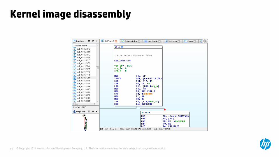
Kernel image disassembly

© Copyright 2014 Hewlett-Packard Development Company, L.P. The information contained herein is subject to change without notice.51
JFFS2 erase marker location from a page and spare column bytes
Identifying the JFFS2 file system from the raw NAND Flash image is relatively easy
Usually JFFS2 puts specialized erasemarkers inside the spare column of each page
ErasemarkerECC Bad block
indicator (FF=Clean)
OOB

© Copyright 2014 Hewlett-Packard Development Company, L.P. The information contained herein is subject to change without notice.52
Mounting JFFS2 file system using a MTD
First, you need to create a MTD device: • Load related Linux kernel modules like
mtdram, mtdblock and JFFS2. This creates a MTD device on the system.
After successful mounting, you can navigate and modify the file system on the fly

© Copyright 2014 Hewlett-Packard Development Company, L.P. The information contained herein is subject to change without notice.53
Writing JFFS2 data
1. Dump mtdblock data to a file
2. Add OOB area• python DumpFlash.py -R -o mtdblock0.oob.dmp
mtdblock0.dmp
3. Program memory at JFFS2 location
• python FlashTool.py -w mtdblock.mod.oob.dmp
-R 0x12820 0xffffffff

© Copyright 2014 Hewlett-Packard Development Company, L.P. The information contained herein is subject to change without notice.54
SMT Re-soldering
After modifying the raw data and writing it back to the Flash memory, re-solder the chip: • The re-soldering process is not much different from usual SMT
soldering • SMT was originally developed for automatic soldering of the PCB
components• The chips are usually small and the pitch of the pins is also relatively
small• Soldering these chips to the PCB manually is challenging, but not
terribly difficult• There are many different methods, but I placed the chip on the pin
location and heated the pins using the soldering iron• The solder residue left from previous de-soldering process melts
again and the chip can be soldered again using this solder• Various other detailed technologies can be found on the Internet

© Copyright 2014 Hewlett-Packard Development Company, L.P. The information contained herein is subject to change without notice.55
Bridge & damaged pins
There are many pitfalls with SMT soldering and one of the big issues is bridging:
• The pitch for NAND flash TSOP48 model is 0.5 mm (which is extremely small). The solder can go over multiple pins and create shorts
One of the big problems with re-soldering is possible damage to the board:
• Excessive heat is applied during desoldering and it can damage the PCB board
• Be extra careful when you re-solder the chips! • Luckily, with Flash memory, many pins are not used at all. If the damaged
patterns are not used, then the chips operate normally• Check with the chip datasheet to see if damaged patterns are used by the
chip

© Copyright 2014 Hewlett-Packard Development Company, L.P. The information contained herein is subject to change without notice.56
My tools
FlashTool – Python Implmentation of Flash reader/writer software• https://github.com/ohjeongwook/DumpFlash/blob/master/FlashTool.py
• Write support
• Fast sequential row read mode support
• More experimental code coming.
Enhanced NandTool (forked from original NandTool): added writing support• https://github.com/ohjeongwook/NANDReader_FTDI
• Write support, which is missing from original NANDTool project from Sprites Mode
DumpFlash.py: Flash image manipulation tool (ECC, Bad block check)• https://github.com/ohjeongwook/DumpFlash/blob/master/DumpFlash.py
DumpJFFS2.py: JFFS2 parsing tool• https://github.com/ohjeongwook/DumpFlash/blob/master/DumpJFFS2.py

© Copyright 2014 Hewlett-Packard Development Company, L.P. The information contained herein is subject to change without notice.57
ConclusionInteracting directly with Flash memory is useful when JTAG can’t be used:• This is increasingly relevant as vendors obfuscate or remove JTAG interfaces to protect their intellectual property
• By directly interacting with the low level Flash memory interface, you can access data that sometimes can’t be retrieved otherwise
The de-soldering method is referred to as destructive, but it is still possible to re-solder the chip to the system using SMT soldering methods:• There is more chance of damaging the circuit board, but the chance of success is still high enough
There are many factors when extracting, modifying and reconstructing a bare metal image with your modification like ECC, bad blocks and JFFS2 erasemarkers: • You might try to modify code from many places like the boot loaders, the kernel or the JFFS2 root image

© Copyright 2014 Hewlett-Packard Development Company, L.P. The information contained herein is subject to change without notice.58
Credits
Original design of NAND reader/writer
Sprites Mod
NANDTool
Sprites Mod and Bjoern Kerlers