resistor equipped transistors (rets): key parameters and
TRANSCRIPT
AN90024Resistor Equipped Transistors (RETs): Key parameters andapplication insightsRev. 1.1 — 3 August 2021 application note
Document informationInformation Content
Keywords RET, polysilicon resistors, digital transistor, pre-biased transistor
Abstract This application note explains specific product and application aspects of Resistor EquippedTransistors (RETs)
Nexperia AN90024Resistor Equipped Transistors (RETs): Key parameters and application insights
1. IntroductionBipolar transistors are controlled via the base current applied. Because of high temperaturedependency of the voltage drop across the base-emitter path, it is required to add at least a seriesresistors at the base for stable and safe operation of a transistor in most applications This isrequired to keep base current at a desired level.
To reduce the number of components and to make board designs less complex, Resistor-EquippedTransistors (RET) have been introduced. These are single or dual transistors with resistorsintegrated on the same die. The integrated resistors have higher tolerances than commonlyused external resistors. This fact makes RETs most suitable for switching applications wherethe transistor operates either in on-state or off-state. This is the reason also, why RETs are oftenreferred to as digital transistors.
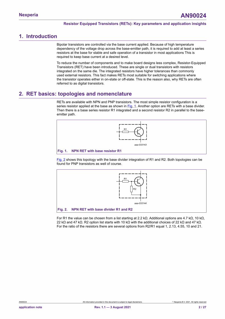
2. RET basics: topologies and nomenclatureRETs are available with NPN and PNP transistors. The most simple resistor configuration is aseries resistor applied at the base as shown in Fig. 1. Another option are RETs with a base divider.Then there is a base series resistor R1 integrated and a second resistor R2 in parallel to the base-emitter path.
aaa-033143
R1
Fig. 1. NPN RET with base resistor R1
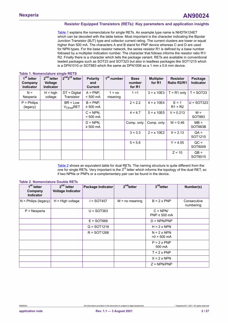
Fig. 2 shows this topology with the base divider integration of R1 and R2. Both topologies can befound for PNP transistors as well of course.
aaa-033144
R1
R2
Fig. 2. NPN RET with base divider R1 and R2
For R1 the value can be chosen from a list starting at 2.2 kΩ. Additional options are 4.7 kΩ, 10 kΩ,22 kΩ and 47 kΩ. R2 option list starts with 10 kΩ with the additional choices of 22 kΩ and 47 kΩ.For the ratio of the resistors there are several options from R2/R1 equal 1, 2.13, 4.55, 10 and 21.
AN90024 All information provided in this document is subject to legal disclaimers. © Nexperia B.V. 2021. All rights reserved
application note Rev. 1.1 — 3 August 2021 2 / 27
Nexperia AN90024Resistor Equipped Transistors (RETs): Key parameters and application insights
Table 1 explains the nomenclature for single RETs. An example type name is NHDTA124ETwhich can be decoded with the table below. Most important is the character indicating the BipolarJunction Transistor (BJT) type and collector current rating. The current clusters are lower or equalhigher than 500 mA. The characters A and B stand for PNP device whereas C and D are usedfor NPN types. For the base resistor network, the series resistor R1 is defined by a base numberfollowed by a multiplier indication number. The character that follows informs the resistor ratio R1/R2. Finally there is a character which tells the package variant. RETs are available in conventionalleaded packages such as SOT23 and SOT323 but also in leadless packages like SOT1215 whichis a DFN1010 or SOT883 which the same as DFN1006 so a 1 mm x 0.6 mm device.
Table 1. Nomenclature single RETS1st letter
CompanyIndicator
2nd letterVoltage
Indicator
2nd3rd letter Polarityand
Current
1st number Basenumberfor R1
Multiplerfor R1
ResistorRatio R2/R1
PackageIndicator
N =Nexperia
H = highvoltage
DT = DigitalTransistor
A = PNP,< 500 mA
1 = nomeaning
1 =1 3 = x 10E3 T = R1 only T = SOT23
P = Philips(legacy)
BR = LowVCEsatRET
B = PNP,≥ 500 mA
2 = 2.2 4 = x 10E4 E = 1R1 = R2
U = SOT323
C = NPN,< 500 mA
4 = 4.7 5 = x 10E5 V = 0.213 M =SOT883
D = NPN,≥ 500 mA
Comp. only: Comp. only: W = 0.46 MB =SOT883B
3 = 3.3 2 = x 10E2 X = 2.13 QA =SOT1215
5 = 5.6 Y = 4.55 QC =SOT8009
Z = 10 QB =SOT8015
Table 2 shows an equivalent table for dual RETs. The naming structure is quite different from theone for single RETs. Very important is the 3rd letter which informs the topology of the dual RET, soif two NPNs or PNPs or a complementary pair can be found in the device.
Table 2. Nomenclature Double RETs1st letter
CompanyIndicator
2nd letterVoltage Indicator
Package Indicator 2ndletter 3rdletter Number(s)
N = Philips (legacy) H = High voltage I = SOT457 M = no meaning B = 2 x PNP Consecutivenumbering
P = Nexperia U = SOT363 C = NPN/PNP ≥ 500 mA
E = SOT666 D = NPN/PNPQ = SOT1216 H = 2 x NPNR = SOT1268 N = 2 x NPN
>0 = 500 mAP = 2 x PNP
500 mAT = 2 x PNPX = 2 x NPN
Z = NPN/PNP
AN90024 All information provided in this document is subject to legal disclaimers. © Nexperia B.V. 2021. All rights reserved
application note Rev. 1.1 — 3 August 2021 3 / 27
Nexperia AN90024Resistor Equipped Transistors (RETs): Key parameters and application insights
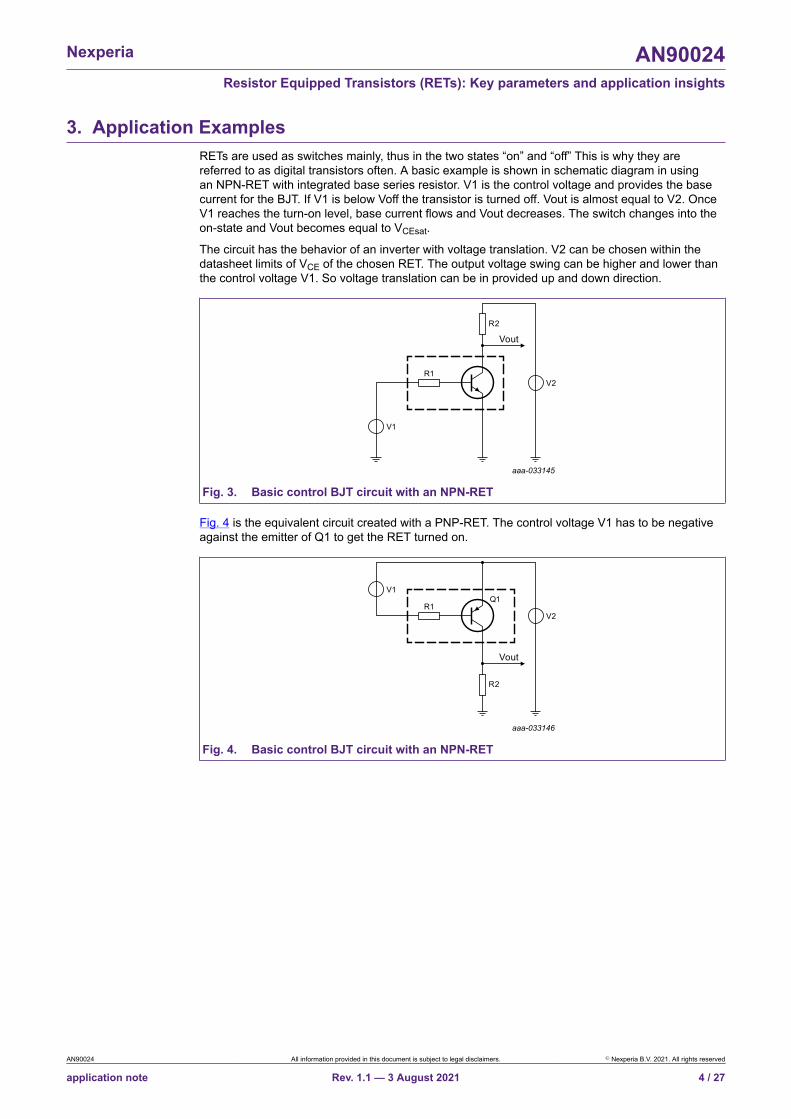
3. Application ExamplesRETs are used as switches mainly, thus in the two states “on” and “off” This is why they arereferred to as digital transistors often. A basic example is shown in schematic diagram in usingan NPN-RET with integrated base series resistor. V1 is the control voltage and provides the basecurrent for the BJT. If V1 is below Voff the transistor is turned off. Vout is almost equal to V2. OnceV1 reaches the turn-on level, base current flows and Vout decreases. The switch changes into theon-state and Vout becomes equal to VCEsat.
The circuit has the behavior of an inverter with voltage translation. V2 can be chosen within thedatasheet limits of VCE of the chosen RET. The output voltage swing can be higher and lower thanthe control voltage V1. So voltage translation can be in provided up and down direction.
aaa-033145
R1
R2
Vout
V1
V2
Fig. 3. Basic control BJT circuit with an NPN-RET
Fig. 4 is the equivalent circuit created with a PNP-RET. The control voltage V1 has to be negativeagainst the emitter of Q1 to get the RET turned on.
aaa-033146
R1
R2
Vout
V1
V2
Q1
Fig. 4. Basic control BJT circuit with an NPN-RET
AN90024 All information provided in this document is subject to legal disclaimers. © Nexperia B.V. 2021. All rights reserved
application note Rev. 1.1 — 3 August 2021 4 / 27

Nexperia AN90024Resistor Equipped Transistors (RETs): Key parameters and application insights
A very common load switch application with RETs in depicted in Fig. 5. The BJT Q2 switches theload current through the load resistor RL. Q2 conducts if Q1 is turned on. The control RET Q1requires a positive base voltage to enable the load switch. The topology does not require high basecurrent nor high voltages for the control signal. Q2 can switch higher load voltages in compliance tothe rating of the chosen component (≤ 80 V) and also comparably high load currents of up to 500mA. Low VCEsat RETs also called Performance-Based RETs (PBR), provide low residual collector-emitter voltages in on-state and therefore achieve high power-efficiency of the load switch. For RETQ2 a product with a base resistor divider achieves a far better turn-off performance compared to aRET with a series resistor in the base-path only. R4 accelerates turn-off time significantly becauseQ2 is driven by an open-collector stage realized by Q1
aaa-033147
R3
RL
Vout
V2V1
Q2
Q1R1
R2
R4
Fig. 5. Load switch with PNP RET in load path and NPN RET in control path
RETs can be used to combine multiple control signals towards one control signal output. Fig. 6shows two input signals V1 and V2 as base drive for two RETs that share one collector resistor.This circuit behaves like a NOR logic function. If one of the inputs is at high level or both, theoutput is providing a low state. Only if both input signals are low the output provides a high-levelsignal. The advantage of such RET solution against a standard logic gate is that the output cansupport high voltages up to 80 V that cannot be found for logic families. The input drive can alsobe designed very flexible via the selection of a suitable base resistor or base voltage divider. Ifrequired, the NOR function can be changed into an OR function by adding an inverter stage asshown in Fig. 1 behind the output of the discussed circuit.
aaa-033148
V1
R1
R2
V2
R3
R4
Vout
V3
R5
Fig. 6. RETs in wired-NOR application
AN90024 All information provided in this document is subject to legal disclaimers. © Nexperia B.V. 2021. All rights reserved
application note Rev. 1.1 — 3 August 2021 5 / 27

Nexperia AN90024Resistor Equipped Transistors (RETs): Key parameters and application insights
In a similar way, a NAND function can be implemented if RETs are connected in series for thecollector-emitter path like shown in Fig. 7. Only if both RETs are turned on at the same time, theoutput signal Vout provides a low level. If the output is inverted by another RET, an AND functionhas been created.
aaa-033149
V1
R1
R2
V2
R3
R4
Vout
V3
R5
Fig. 7. RETs in wired-NAND application
In Fig. 8 an application example for a push-pull stage is shown. The circuit is powered by twovoltage sources V2 and V3, providing a negative and positive polarity supply. Vout is terminated toground via Rload, which is the connection between the two voltage sources. Q1 and Q2 work asemitter followers and amplify current provided by the input source V1.
aaa-033150
V1
R1Q1
R2
Vout Rload
V3
R3
Q2
R4
V2
Fig. 8. Application example push-pull stage with RETs
AN90024 All information provided in this document is subject to legal disclaimers. © Nexperia B.V. 2021. All rights reserved
application note Rev. 1.1 — 3 August 2021 6 / 27

Nexperia AN90024Resistor Equipped Transistors (RETs): Key parameters and application insights
4. Data sheet parametersIn this chapter the Nexperia data sheets for RETs are explained in detail. The major focus is on theelectrical parameters. For the discussion in this chapter a rather new Nexperia high voltage REThas been chosen from an 80 V product series for reference.
The first chapter is the “General Description”. It informs the BJT polarity of the RET and thepackages available. Table 3 shows the product overview with the resistor variants R1/R2 of thechosen component. The complementary parts are mentioned if applicable.
Table 3. Product overviewR1 R2 PackageType numberkΩ kΩ Nexperia JEITA
PNP complement:
NHDTC114EU 10 10 NHDTA114EUNHDTC124EU 22 22 NHDTA124EUNHDTC144EU 47 47
SOT323 SC-70
NHDTA144EU
A list of “Features and benefits” follows in the next section with. The major features like currentcapability, high break down voltage and automotive qualification are mentioned here.
Features and benefits
• 100 mA output current capability• High breakdown voltage• Built-in resistors• Simplifies circuit design• Reduces component count• Reduces pick and place costs• AEC-Q101 qualified
The following section informs major application areas, . These are digital or switching applicationsas discussed in more detail the prior chapter.
Applications
• Digital applications• Cost saving alternative for BC846 series in digital applications• Controlling IC inputs• Switching loads
“Quick reference data” are depicted in a brief table with electrical key parameters such asmaximum allowed VCE0 and output current IO.
Table 4. Quick reference dataTamb = 25 °C unless otherwise specified.
Symbol Parameter Conditions Min Typ Max UnitVCEO collector-emitter voltage open base - - 80 VIO output current - - 100 mA
AN90024 All information provided in this document is subject to legal disclaimers. © Nexperia B.V. 2021. All rights reserved
application note Rev. 1.1 — 3 August 2021 7 / 27

Nexperia AN90024Resistor Equipped Transistors (RETs): Key parameters and application insights
The pinout of the RET is informed with the emitter, collector and input connections as shown below.The input pin is also referred to as base although there are resistors integrated in between.
Table 5. PinningPin Symbol Description Simplified outline Graphic symbol1 I input (base)2 GND GND (emitter)3 O output (collector)
1 2
3
aaa-019964
O
GND
IR1
R2
The next section contains the ordering information.
Table 6. Ordering informationPackageType numberName Description Version
NHDTC114EUNHDTC124EUNHDTC144EU
SC-70 plastic surface-mounted package; 3 leads SOT323
The marking table in informs the marking of the devices. The last character “%” is a placeholder forthe manufacturing site.
Table 7. MarkingType number Marking code [1]NHDTC114EU 5M%NHDTC124EU 5Q%NHDTC144EU 5S%
[1] % = placeholder for manufacturing site code
AN90024 All information provided in this document is subject to legal disclaimers. © Nexperia B.V. 2021. All rights reserved
application note Rev. 1.1 — 3 August 2021 8 / 27

Nexperia AN90024Resistor Equipped Transistors (RETs): Key parameters and application insights
The limiting values follow in the next section of the RET data sheet in Table 8.
VCB0 is the maximum collector-base voltage with an open emitter pin. VCE0 is the maximum allowedcollector-emitter voltage with an open base. For a RET where a resistor is placed between baseand emitter it could be called VCER as well because the input of the RET is open, but not the baseof the BJT. There is the relation to be considered for the breakdown voltage of the collector-emitterpath of a BJT as shown below:
VCES ≥ VCER ≥ VCE0
VCES is tested with the base being short-circuit to the emitter. For RETs the integrated resistors arenot taken into account for the nomenclature of parameters. Despite of integrated resistors the termVCEO is used still. This is important to be taken into account for other key parameters as well likeleakage current ratings.
VI has a maximum rating of 10 V for the example data sheet of a PNP RET with a divider ratio of 1.The BJT as a stand-alone device would have the limitation of VEB0 = 5 V. Due to the input dividerthis value is doubled. The base-emitter diode is driven reverse and therefore does not conductbelow the limit value. For further details please refer to chapter 5.
For the other polarity of VI, base current flows, so there is a forward voltage drop across the base-emitter diode to be considered whereas the rest of the input voltage is present at the base seriesresistor R1. The voltage limit is mainly defined by the maximum power dissipation of the integratedresistor R1. Therefore maximum base current is limited by R1 and thus VI.
Total power dissipation Ptot is informed for two mounting conditions. One is meant for a single layerFR4-PCB using a standard footprint. The second value is provided for a 4-layer FR4-PCB, wherebottom layer and the inside layers are solid copper planes.
Table 8. Limiting valuesIn accordance with the Absolute Maximum Rating System (IEC 60134).Tamb = 25 °C unless otherwise specified.
Symbol Parameter Conditions Min Max UnitVCBO collector-base voltage open emitter - 80 VVCEO collector-emitter voltage open base - 80 VVEBO emitter-base voltage open collector - 10 V
input voltageNHDTC114EU -10 +40 VNHDTC124EU -10 +60 V
VI
NHDTC144EU -10 +80 VIO output current - 100 mA
[1] - 235 mWPtot total power dissipation Tamb ≤ 25 °C[2] - 315 mW
Tj junction temperature - 150 °CTamb ambient temperature -55 150 °CTstg storage temperature -65 150 °C
[1] Device mounted on an FR4 Printed-Circuit-Board (PCB); single-sided copper; tin-plated and standard footprint.[2] Device mounted on an FR4 Printed-Circuit-Board (PCB);4-layer copper; tin-plated and standard footprint.
The maximum junction temperature for gold wire products is 150°C because otherwise the aluminalayer of the bond wire joint would be consumed up by diffusion processes of the alumina into thegold. For longer exposure to temperatures above 150°C the wire joint becomes unstable and canfail. Copper wire products can be specified up to 175°C. Storage and ambient temperature havethe same limits. With rising ambient temperature the maximum power that can be applied degradeswith a linear curve as shown in Fig. 9 below. A RET which is designed for Tj(max) = 175°C has aderating curve which reaches the x-axis at 175°C, so higher power can be dissipated comparably.
AN90024 All information provided in this document is subject to legal disclaimers. © Nexperia B.V. 2021. All rights reserved
application note Rev. 1.1 — 3 August 2021 9 / 27

Nexperia AN90024Resistor Equipped Transistors (RETs): Key parameters and application insights
Tamb (°C)-75 17512525 75-25
aaa-031869
200
100
300
400
Ptot(mW)
0
(1)
(2)
(1) FR4 PCB, 4-layer copper, standard footprint(2) FR4 PCB, single-sided copper, standard footprint
Fig. 9. Power derating curves SOT323 (SC-70)
AN90024 All information provided in this document is subject to legal disclaimers. © Nexperia B.V. 2021. All rights reserved
application note Rev. 1.1 — 3 August 2021 10 / 27

Nexperia AN90024Resistor Equipped Transistors (RETs): Key parameters and application insights
Further thermal characteristics are provided in Table 9 in the example RET data sheet. Thermalresistance Rth is informed for different mounting conditions. The values provided could also becalculated from the related Ptot ratings in Tab. 6 with:
Rth(j-a) = (Tj(max) – 25°C)/Ptot
For example for Rth(j-a) the calculation delivers:
(150 °C - 25 °C)/0.235 W = 532 K/W
Table 9. Thermal characteristicsTamb = 25 °C unless otherwise specified.
Symbol Parameter Conditions Min Typ Max Unit[1] - - 532 K/WRth(j-a) thermal resistance from junction to ambient in free air[2] - - 397 K/W
Rth(j-sp) thermal resistance from junction to solder point - - 150 K/W
[1] Device mounted on an FR4 Printed-Circuit-Board (PCB); single-sided copper; tin-plated and standard footprint.[2] Device mounted on an FR4 Printed-Circuit Board (PCB), 4-layer copper, tin-plated and standard footprint.
Rth(j-sp) is the thermal resistance from junction to the solder point of the pin for the major thermalpath of the SMD package discussed. For RETs in SOT23 or SOT323 this is the collector lead.The other two terminals for the emitter and base are connected via bond wires, so they do notcontribute to heat dissipation. Rth(j-a) informs about the thermal resistance from junction to ambient.This value depends significantly on the mounting condition, for example PCB layout and type aswell as copper thickness.
Zth(j-a) is the transient thermal impedance from junction to ambient as depicted in Fig.8 and Fig.9.These diagrams help to calculate a thermal scenario for applications where the RET is not run inDC condition but where it operates in switching mode.
The Zth diagrams are provided for different mounting conditions. Zth is provided versus the pulselength of the on-state for the RET. Curves are depicted for different duty cycles d from single eventswith d = 0 up to DC mode with d = 1. Duty cycle d is defined as:
d = ton /T, where ton is the on-state duration and T the cycle time.
The value for the DC-case is identical to the Rth(j-a) parameter in the data sheet. For long pulseswith about more than 10 seconds duration rather small SMD components get heated up to thesame temperature like for a constant on-state. This is why all curves start at the same level on theright side of the diagrams. If short pulses are applied, the values for Zth are becoming smaller, sohigher pulse power can be handled. The curves are getting flat for very short pulses and d > 0.05in the diagram. This is the case because switching frequency is becoming quite high in this regionand the heat generation is averaging out in the crystal. There is almost no time for temperaturechanges between on-state and off-state.
AN90024 All information provided in this document is subject to legal disclaimers. © Nexperia B.V. 2021. All rights reserved
application note Rev. 1.1 — 3 August 2021 11 / 27
Nexperia AN90024Resistor Equipped Transistors (RETs): Key parameters and application insights
aaa-031870
10-5 1010-210-4 10210-1tp (s)
10-3 1031
102
10
103
Zth(j-a)(K/W)
1
duty cycle = 10.75
0.500.33
0.20
0.01
0.10
0.05
0
0.02
FR4 PCB, single-sided copper, tin-plated and standard footprint
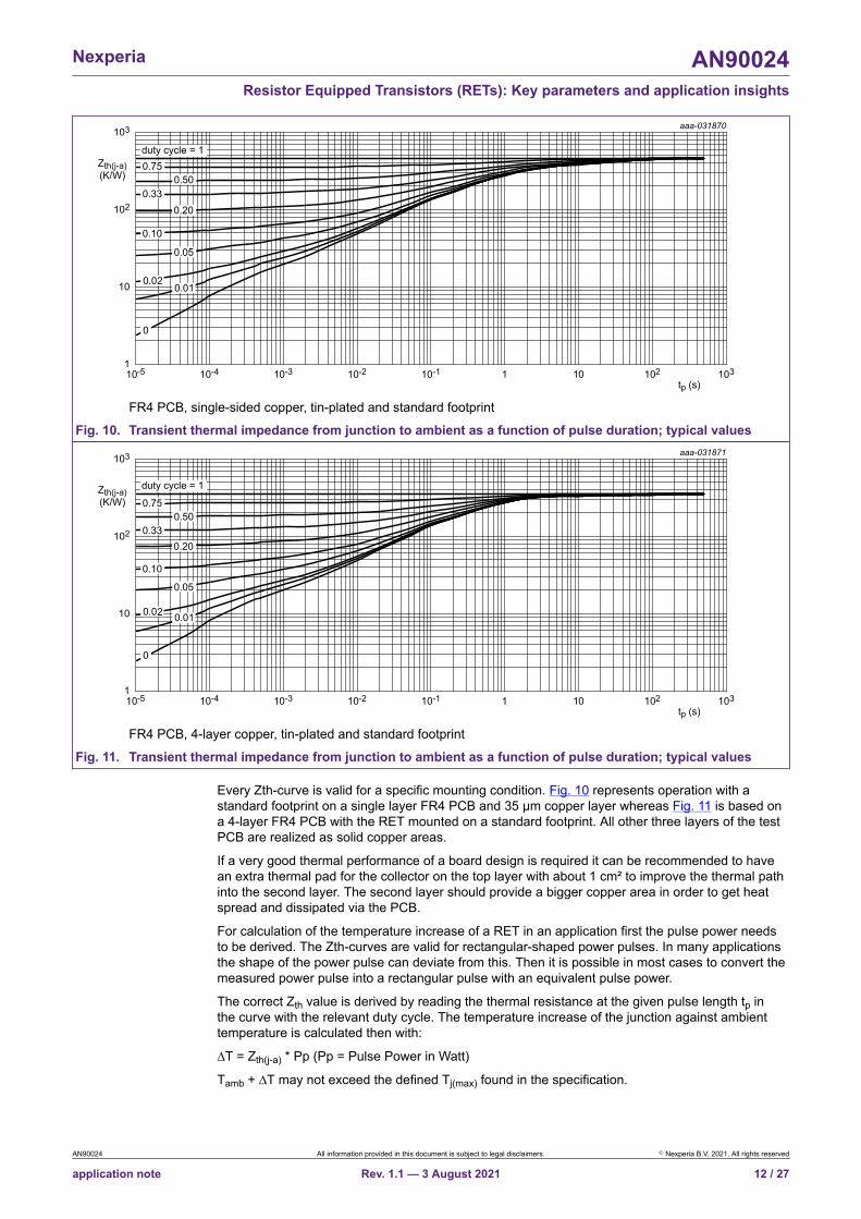
Fig. 10. Transient thermal impedance from junction to ambient as a function of pulse duration; typical valuesaaa-031871
10-5 1010-210-4 10210-1tp (s)
10-3 1031
102
10
103
Zth(j-a)(K/W)
1
duty cycle = 1
0.750.50
0.330.20
0.01
0.10
0.05
0.02
0
FR4 PCB, 4-layer copper, tin-plated and standard footprint
Fig. 11. Transient thermal impedance from junction to ambient as a function of pulse duration; typical values
Every Zth-curve is valid for a specific mounting condition. Fig. 10 represents operation with astandard footprint on a single layer FR4 PCB and 35 µm copper layer whereas Fig. 11 is based ona 4-layer FR4 PCB with the RET mounted on a standard footprint. All other three layers of the testPCB are realized as solid copper areas.
If a very good thermal performance of a board design is required it can be recommended to havean extra thermal pad for the collector on the top layer with about 1 cm² to improve the thermal pathinto the second layer. The second layer should provide a bigger copper area in order to get heatspread and dissipated via the PCB.
For calculation of the temperature increase of a RET in an application first the pulse power needsto be derived. The Zth-curves are valid for rectangular-shaped power pulses. In many applicationsthe shape of the power pulse can deviate from this. Then it is possible in most cases to convert themeasured power pulse into a rectangular pulse with an equivalent pulse power.
The correct Zth value is derived by reading the thermal resistance at the given pulse length tp inthe curve with the relevant duty cycle. The temperature increase of the junction against ambienttemperature is calculated then with:
∆T = Zth(j-a) * Pp (Pp = Pulse Power in Watt)
Tamb + ∆T may not exceed the defined Tj(max) found in the specification.
AN90024 All information provided in this document is subject to legal disclaimers. © Nexperia B.V. 2021. All rights reserved
application note Rev. 1.1 — 3 August 2021 12 / 27

Nexperia AN90024Resistor Equipped Transistors (RETs): Key parameters and application insights
The next chapter in data sheets of RETs informs the electrical characteristics of the components.Most characteristics are tested at an ambient temperature of 25° C unless another temperature isinformed for the test conditions. If the test condition can heat up the device significantly, the relatedvalue is measured in a pulsed test mode in order to avoid self-heating.
Table 10. CharacteristicsTamb = 25 °C unless otherwise specified.
Symbol Parameter Conditions Min Typ Max UnitV(BR)CBO collector-base
breakdown voltageIC = 100 µA; IE = 0 A 80 - - V
V(BR)CEO collector-emitterbreakdown voltage
IC = 2 mA; IB = 0 A 80 - - V
ICBO collector-base cut-offcurrent
VCB = 80 V; IE = 0 A - - 100 nA
VCE = 60 V; IB = 0 A - - 100 nAICEO collector-emitter cut-offcurrent VCE = 60 V; IB = 0 A; Tj = 150 °C - - 5 µAemitter-base cut-off currentNHDTC114EU - - 600 µANHDTC124EU - - 270 µA
IEBO
NHDTC144EU
VEB = 7 V; IC = 0 A
- - 130 µADC current gainNHDTC114EU 50 - -NHDTC124EU 70 - -
hFE
NHDTC144EU
VCE = 5 V; IC = 10 mA
100 - -VCEsat collector-emitter
saturation voltageIC = 10 mA; IB = 0.5 mA - - 100 mV
VI(off) off-state input voltage VCE = 5 V ; IC = 100 µA - 1.15 0.8 Von-state input voltageNHDTC114EU 2.5 1.8 - VNHDTC124EU 3 2.3 - V
VI(on)
NHDTC144EU
VCE = 0.3 V ; IC = 10 mA
5 3.3 - Vbias resistor 1 (input) [1]NHDTC114EU 7 10 13 kΩNHDTC124EU 15.4 22 28.6 kΩ
R1
NHDTC144EU 33 47 61 kΩR2/R1 bias resistor ratio [1] 0.8 1 1.2fT transition frequency VCE = 5 V; IC = 10 mA; f = 100 MHz [2] - 170 - MHzCc collector capacitance VCB = 10 V; IE = ie = 0 A; f = 1 MHz - - 2.5 pF
[1] See section "Test information" for resistor calculation and test conditions[2] Characteristics of built-in transistor
Table 10 starts with the break down voltages V(BR)CBO and V(BR)CEO, means break down voltagesof the collector-base path with an open emitter respectively collector-emitter path with an openbase.
Maximum leakage currents ICBO, ICEO and IBEO are informed next. These are the cut-off currentsfor the collector-base, collector emitter and base-emitter path. The emitter-base cut-off currentvalues appear quite high compared to a stand-alone BJT. The reason for this is that the integratedbase resistors are located across this path. If an R2 resistor is present, the leakage current isproportional to the sum of R1 and R2 at the specified conditions.
AN90024 All information provided in this document is subject to legal disclaimers. © Nexperia B.V. 2021. All rights reserved
application note Rev. 1.1 — 3 August 2021 13 / 27

Nexperia AN90024Resistor Equipped Transistors (RETs): Key parameters and application insights
The hFE parameters for RETs are defined as IC/IIN. IIN is divided into the base current and thecurrent which flows through R2 which is IR2 = VBE/R2. Due to this fact hFE is smaller comparedto a RET with a series base resistor R1 only. And of course hFE is getting smaller the lower theresistance of R2 is, because input current is drained away. This fact can be seen in Table 10clearly.
VCEsat is the residual collector-emitter voltage in on-state of the RET switch. The test condition is toapply 0.5 mA base drive and 10 mA collector current.
VI considerations
VI(off) informs at which input voltage the RET turns off. The test condition for off-state is to have acollector leakage current of 100 µA at a collector-emitter voltage of 5 V. The lower value providedin the table as V(Ioff)max has to be considered as maximum allowed output level of the stage whichdrives the RET. This condition has to be fulfilled for safe off-state of the RET.
For the other direction, the on-state, there is the important parameter VI(on)min to be considered.The circuit controlling the RET has to provide this voltage for a safe turn on at least. As on-statecondition a collector current of 10 mA is defined while the collector-emitter voltage is 0.3 V. Thedata sheet VI rating is valid for the test condition defined only. If a bigger collector current shall beswitched the RET requires more base drive voltage VI(on).
In Fig. 12 the switching characteristic of a RET is shown with a graph of VCE versus VI.
VI < VI(off)max: a RET is in off-state for every device shipped.
VI < VI(off)typ: a typical RET is in off-state.
VI > VI(on)typ: a typical RET is in on-state.
VI > VI(on)min: a RET is in on-state for every device shipped.
Fig. 12. RET Input voltage VI versus VCEcharacteristics
aaa-033151Input voltage
Off
On
VI(off)max VI(off)typ VI(on)typ
VCE
VI(on)min
AN90024 All information provided in this document is subject to legal disclaimers. © Nexperia B.V. 2021. All rights reserved
application note Rev. 1.1 — 3 August 2021 14 / 27

Nexperia AN90024Resistor Equipped Transistors (RETs): Key parameters and application insights
Table 11 shows the dependency of the on- and off-state input voltages on the resistor dividerconfiguration in RETs from the NHDTC series.
For the VI(off) condition a very small base current flows into the BJT (about 0.3 µA) . So the typicalvalue to turn off a RET is coupled almost directly to the resistor ratio R1/R2. It can be calculatedwith a voltage drop target across R2 or the base-emitter diode where the transistor is turned off.This voltage is about 580 mV for the NHDTC series discussed. Therefore VI(off) values for a resistorratio equal 1 show the same voltages (rows 1-3 in Table 11).
The typical off-state voltages for R2 equal 47 kΩ and different R1 (2.2 kΩ, 4.7 kΩ and 10 kΩ ) arelower in accordance with the above described background. For VI(off) max an even value has beendefined which safeguards operation in the very left area of Fig. 12.
Table 11. VI(on) and VI(off) dependency on resistor configuration R1/R2R1 / R2
(kΩ)VI(on) min
(V)VI(on) typ
(V)VI(on) max
(V)VI(off) max
(V)RET Type
10 / 10 2.5 1.8 1.15 0.8 NHDTC114ET22 / 22 3 2.3 1.15 0.8 NHDTC124ET47 / 47 5 3.3 1.15 0.8 NHDTC144ET2.2 / 47 1.2 0.81 595 0.5 NHDTC123JT4.7 / 47 1.4 0.95 625 0.5 NHDTC114YT10 / 47 1.6 1.22 690 0.5 NHDTC143ZT
The selection of a proper resistor divider option is important so that the control voltage window ofthe RET fits well to the driving stage. The desired collector or load current has an impact on thebase current to be provided for the on-state. For a higher collector current a lower value for R1 and/or less bypass current through R2 is the direction to go.
For an application, temperature drift of the VI parameters needs some attention. VBE of BJTsdecreases over temperature with a coefficient of about -1.7 mV/K to -2.1 mV/K dependent onchosen silicon diffusion details.
Current amplification hFE = IC/IB increases with about 1% per Kelvin for a stand-alone BJT.
AN90024 All information provided in this document is subject to legal disclaimers. © Nexperia B.V. 2021. All rights reserved
application note Rev. 1.1 — 3 August 2021 15 / 27

Nexperia AN90024Resistor Equipped Transistors (RETs): Key parameters and application insights
In Fig. 13 the typical DC current gain as a function of collector current is shown for the ambienttemperatures 100 °C, 25 °C and -40 °C. Also for a RET with integrated poly-silicon resistor basedivider, hFE shows higher values the warmer Tamb becomes.
IC (mA)10-1 102101
aaa-031707
102
10
103
hFE
1
(3)
(2)
(1)
VCE = 5 V(1) Tamb = 100 °C(2) Tamb = 25 °C(3) Tamb = -40 °C
Fig. 13. NHDTC144EU: DC current gain as a function of collector current; typical values
In Fig. 14 of the data sheet, the typical On-state input voltage VI(on) is shown as a function ofIC. As to be expected a higher input voltage is required to drive more collector current at sameVCE. A low ambient temperature requires higher input voltage because VBE increases and hFEdrops. So turning on a RET switch at low temperature is the most critical operating condition for anapplication and the user has to apply enough input voltage in order to turn on the device properly.
IC (mA)10-1 102101
aaa-031709
10
1
102
VI(on)(V)
10-1
(1)
(3)
(2)
VCE = 0.3 V(1) Tamb = -40 °C(2) Tamb = 25 °C(3) Tamb = 100 °C
Fig. 14. NHDTC144EU: On-state input voltage as a function of collector current; typicalvalues
AN90024 All information provided in this document is subject to legal disclaimers. © Nexperia B.V. 2021. All rights reserved
application note Rev. 1.1 — 3 August 2021 16 / 27

Nexperia AN90024Resistor Equipped Transistors (RETs): Key parameters and application insights
Fig. 15 of the data sheet shows which VI(off) has to be applied typically to guarantee a safe turnoff of a RET switch. For this switching direction the input voltage has to be low enough for safeoperation. For the off-state high temperature condition is the most critical scenario. In this case thedriver circuit has to be designed in a way that it outputs a voltage well below typical VI(off) for thehighest temperature in the application.
aaa-031710
IC (mA)10-1 102101
1
10
VI(off)(V)
10-1
(1)
(3)
(2)
VCE = 5 V(1) Tamb = -40 °C(2) Tamb = 25 °C(3) Tamb = 100 °C
Fig. 15. NHDTC144EU: On-state input voltage as a function of collector current; typicalvalues
5. RET resistor specificsR1, the series resistor towards the base of the BJT has a tolerance of typically +/- 30 %.
R2 is not defined directly but via a ratio R2/R1. This has a tolerance of ± 20% for 100 mA RETs and± 10% for 500 mA RETs as depicted in Table 12 below.
Table 12. Tolerances of integrated resistors in RETsResistor specification Typical tolerances RET types
R1 ± 30% allR2/R1 ± 20% 100 mA RETs
± 10% 500 mA RETs
This means for the range of R1:
R1min = 0.7 * R1typ
R1max = 1.3 * R1typ
For calculating the minimum and maximum values of R2, the tolerance for the resistor ratio has tobe considered. For 100 mA RETs it can be calculate with ± 20% tolerance according Tab.9:
R2min = 0.7 * R1typ * 0.8 * R2typ/R1typ = 0.56 * R2typ
R2max = 1.3 * R1typ * 1.2 * R2typ/R1typ = 1.56 * R2typ
The temperature dependency of the integrated polysilicon resistors can be described with thequadratic equation below. T0 is 25°C for the values provided in Tab. 10.
R(T) = R(T0) * ( 1 + α * (T – T0) + β * (T – T0)²)
AN90024 All information provided in this document is subject to legal disclaimers. © Nexperia B.V. 2021. All rights reserved
application note Rev. 1.1 — 3 August 2021 17 / 27

Nexperia AN90024Resistor Equipped Transistors (RETs): Key parameters and application insights
Table 13 informs the coefficients α and β for Phosphorus-doped Poly-Silicon which is used forgeneration 1 RETs in Nexperia and Boron-doped Poly-Silicon used for generation 2 wafers. Fig. 16shows the normalized resistance over temperature for these two process options. The resistance ofthe integrated resistors decreases over temperature. The Boron-doped Poly-Silicon resistor show asmaller temperature dependance compared to the Phosphorus doping.
Table 13. Coefficients for thermal dependency of Poly-Silicon resistor values in RETsα β
Phosphorus-doped Poly-Si -0.00229 7.26 * 10E-6Boron-doped Poly-Si -0.00161 3.7275 * 10E-6
Fig. 16. Normalized resistance over temperature for Nexperia RETs
Temperature (°C)-60 10020-20 14060-40 120400 16080
aaa-0331521.25
R(T)/R25
0.80
0.85
0.90
0.95
1.00
1.05
1.10
1.15
1.20Gen 1: Phosphrous-doped Poly-SiGen 2: Boron-doped Poly-Si
There are two more parameters in RET data sheets, (see Table 10) which are related to thedynamic performance of these components; transition frequency fT and collector capacitanceCc. fT is the frequency where the current amplification of the BJT becomes equal to 1 for the testcondition defined.
AN90024 All information provided in this document is subject to legal disclaimers. © Nexperia B.V. 2021. All rights reserved
application note Rev. 1.1 — 3 August 2021 18 / 27
Nexperia AN90024Resistor Equipped Transistors (RETs): Key parameters and application insights
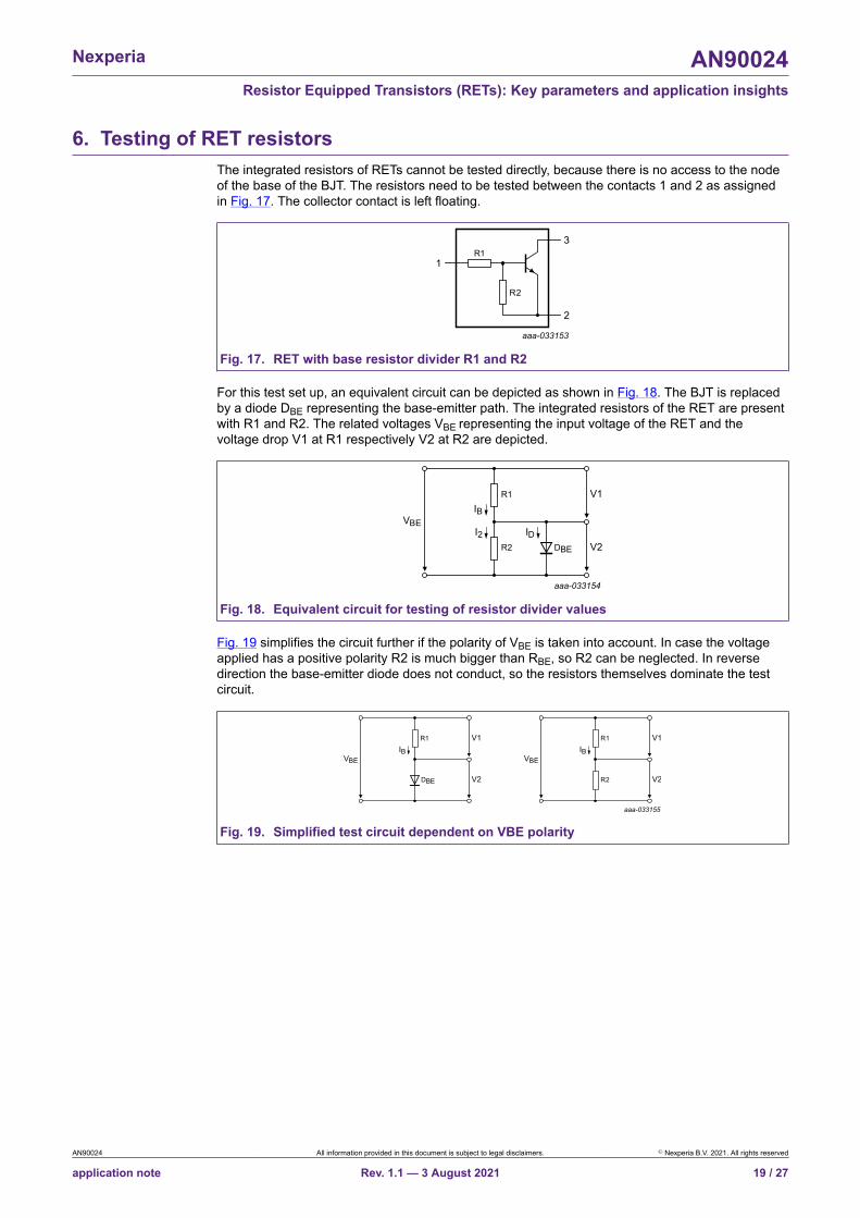
6. Testing of RET resistorsThe integrated resistors of RETs cannot be tested directly, because there is no access to the nodeof the base of the BJT. The resistors need to be tested between the contacts 1 and 2 as assignedin Fig. 17. The collector contact is left floating.
aaa-033153
R1
R2
1
3
2
Fig. 17. RET with base resistor divider R1 and R2
For this test set up, an equivalent circuit can be depicted as shown in Fig. 18. The BJT is replacedby a diode DBE representing the base-emitter path. The integrated resistors of the RET are presentwith R1 and R2. The related voltages VBE representing the input voltage of the RET and thevoltage drop V1 at R1 respectively V2 at R2 are depicted.
aaa-033154
VBE
V1
V2
IBR1
R2 DBE
I2 ID
Fig. 18. Equivalent circuit for testing of resistor divider values
Fig. 19 simplifies the circuit further if the polarity of VBE is taken into account. In case the voltageapplied has a positive polarity R2 is much bigger than RBE, so R2 can be neglected. In reversedirection the base-emitter diode does not conduct, so the resistors themselves dominate the testcircuit.
VBE
V1
V2
IBR1
DBE
aaa-033155
VBE
V1
V2
IBR1
R2
Fig. 19. Simplified test circuit dependent on VBE polarity
AN90024 All information provided in this document is subject to legal disclaimers. © Nexperia B.V. 2021. All rights reserved
application note Rev. 1.1 — 3 August 2021 19 / 27

Nexperia AN90024Resistor Equipped Transistors (RETs): Key parameters and application insights
Fig. 20 shows an I-V-curve of the base-emitter path, so VBE versus the input current IB, for an NPN-RET with an R1 of 2.2 kΩ and R2 of 47 kΩ. The diagram is separated into 4 regions.
Region IV corresponds to reverse direction VBE, where in addition breakdown voltage of the base-emitter diode is exceeded. The steepness or dynamic resistance ∆V/∆I in this part of the curve isR1, because the emitter-base diode clamps to the breakdown voltage.
Region III is the reverse blocking voltage range equivalent to the right part of Fig. 18. Thesteepness is equivalent to R1 + R2. This value is tested in mass production under this condition.Nexperia uses a two point testing method for a more exact measurement result, so R1 + R2 =∆VBE/∆IB.
In Region II the VBE path is biased in forward direction but the base-emitter diode is not conductingsignificantly yet. The steepness of the curve is proportional to R1 + R2 like for Region III.
In Region I the diode conducts as depicted on the right side of Fig. 18. The curve ramps up withR1 as steepness. To measure the steepness two operating points have to be chosen in order tocalculate ∆VBE/∆IB. R1 is measured following this test method in mass production. In Region Isingle operating point measurement would not be sufficient because Vf of the base-emitter diodecreates an voltage offset of the curve that needs to be eliminated for resistor calculation. Fig. 21shows an example where the two test points provide a good result for R1, with R1 = (V2 -V1) / (IB2-IB1) as they are in the linear region of the curve.
With the value for R1 + R2 derived from Region III, R2 can be calculated easily and the ratio R2/R1as well.
VBE (V)-10 4
aaa-0331563.0 mIB(A)
-500.0 µ
Region IV
0.0
500.0 µ
1.0 m
1.5 m
2.0 m
2.5 m
-8 -6 -4 -2 2
Region IRegion II
Region III
0
Fig. 20. Typical VBE versus IB curve for a RET with R1 = 2.2 kΩ and R2 = 47 kΩ
VBE (V)1.4
aaa-033157400 µIB(A)
0 µ0.2 0.4 0.6 0.8 1.2
Region IRegion II
1.0
50 µ
100 µ
150 µIB2
IB1
200 µ
250 µ
300 µ
350 µ
0.0
Fig. 21. Example for two test points on the I-V curve in Region I for calculation of theintegrated resistor R1
AN90024 All information provided in this document is subject to legal disclaimers. © Nexperia B.V. 2021. All rights reserved
application note Rev. 1.1 — 3 August 2021 20 / 27

Nexperia AN90024Resistor Equipped Transistors (RETs): Key parameters and application insights
7. RETs exposed to ESD eventsBipolar transistors have a rather good ESD robustness compared to small size MOSFETtransistors. For MOSFETs the gate is the most vulnerable pin because gate oxide can getdamaged quite easily without a recovery from an exposure to surge events above the breakthroughvoltage. This is why most small-signal MOSFETs have an integrated gate-source ESD protectionnowadays. The ESD robustness level which is targeted for electronic components has the goal tosecure safe handling in mounting and board production. A standard level of robustness is a 2 kVHBM (human body model) rating for ICs and discrete electronic components.
Discrete BJTs meet the target of a 2 kV HBM robustness without problems normally because pn-junctions facing a breakdown are not damaged if current and energy applied is comparably low.
In contrast RETs require some attention for ESD events because the integrated poly-siliconresistors tend to be sensitive to surge pulses. This fact is not specific for any semiconductormanufacturer in the market but requires general attention.
ESD damages can be seen at the resistor R1 most often. R2 is protected via the base-emitterdiode of the BJT which does either conduct in forward direction or clamps an incoming surge eventto a non-destructive level in reverse direction. Fig. 22 shows typical ESD related crystal damagesin the base resistor R1.
Fig. 22. Example for two test points on the I-V curve in Region I for calculation of theintegrated resistor R1
In modern ESD-safe manufacturing environment RETs can be mounted safely. If the base isattached to an interface for external connections, an additional external ESD protection might beconsidered.
AN90024 All information provided in this document is subject to legal disclaimers. © Nexperia B.V. 2021. All rights reserved
application note Rev. 1.1 — 3 August 2021 21 / 27

Nexperia AN90024Resistor Equipped Transistors (RETs): Key parameters and application insights
8. Package overview for Nexperia RETsNexperia offers RETs in various package options. Table 14 shows the package types availableclustered into leaded and leadless types. The size of the package body is informed as well as thepower rating for a standard footprint on a single layer FR4 PCB.
The table shows that leadless packages provide a very good thermal performance while savingboard space. A DFN1006 RET performs as well as a much bigger SOT23 device. With aDFN1412-6 RET up to 480 mW can be dissipated with a package area of 1.4 mm x 1.2 mm =1.68 mm² compared to 400 mW for a SOT457 and a much bigger package area of 4.35 mm². TheDFN1412 is 40% of the size of a SOT457 for the package body. In a design the occupied areais even more important to be compared. For DFN1412 the occupied area is 1.6 mm x 1.71 mm= 2.736 mm². For SOT457 the area 5.3 mm x 5.05 mm = 26.765 mm² needs to be provided on aboard. So space saving is enormous for the DFN package as the factor is close to 10. The reasonis that the leads itself and the landing pads of a leaded package require significant extra spacecompared to a leadless device where the landing pads are almost under the package with smallareas outside the package body.
The thermal path from the crystal down into the PCB is short and direct. This is why Rth(j-sp) isvery small for DFN devices. Leadless packages allow a more compact design combined with ahigh power density. This helps designers to have a suitable solution for the industry trend towardsfurther miniaturization.
Table 14. Package options for RETsPackagecluster
Packagename
RETtype
Size(mm)
Ptot(mW)
[1]SOT23 single 2.9 x 1.3 x 1 250
SOT323 single 2 x 1.25 x 0.95 235SOT457 dual 2.9 x 1.5 x 1 400 (250)SOT363 dual 2 x 1.25 x 095 350 (235)
leaded
SOT666 dual 1.6 x 1.2 x 0.55 300 (200)DFN1006-3(SOT883)
single 1 x 0.6 x 0.48 250
DFN1006B-3(SOT883B)
single 1 x 0.6 x 0.37 250
DFN1010D-3(SOT1215)
single 1.1 x 1 x 0.37 325
DFN1010B-6(SOT1216)
dual 1.1 x 1 x 0.37 350 (230)
leadless
DFN1412-6(SOT1268-1)
dual 1.4 x 1.2 x 0.47 480 (325)
[1] For dual types the first value is maximum power per device and the value in brackets is valid pertransistor.
AN90024 All information provided in this document is subject to legal disclaimers. © Nexperia B.V. 2021. All rights reserved
application note Rev. 1.1 — 3 August 2021 22 / 27
Nexperia AN90024Resistor Equipped Transistors (RETs): Key parameters and application insights
9. Revision historyTable 15. Revision historyRevisionnumber
Date Description
1.1 20210803 Minor formating corrections.1.0 20210303 AN90024 initial version
AN90024 All information provided in this document is subject to legal disclaimers. © Nexperia B.V. 2021. All rights reserved
application note Rev. 1.1 — 3 August 2021 23 / 27
Nexperia AN90024Resistor Equipped Transistors (RETs): Key parameters and application insights
10. Legal information
DefinitionsDraft — The document is a draft version only. The content is still underinternal review and subject to formal approval, which may result inmodifications or additions. Nexperia does not give any representations orwarranties as to the accuracy or completeness of information included hereinand shall have no liability for the consequences of use of such information.
DisclaimersLimited warranty and liability — Information in this document is believedto be accurate and reliable. However, Nexperia does not give anyrepresentations or warranties, expressed or implied, as to the accuracyor completeness of such information and shall have no liability for theconsequences of use of such information. Nexperia takes no responsibilityfor the content in this document if provided by an information source outsideof Nexperia.
In no event shall Nexperia be liable for any indirect, incidental, punitive,special or consequential damages (including - without limitation - lostprofits, lost savings, business interruption, costs related to the removalor replacement of any products or rework charges) whether or not suchdamages are based on tort (including negligence), warranty, breach ofcontract or any other legal theory.
Notwithstanding any damages that customer might incur for any reasonwhatsoever, Nexperia’s aggregate and cumulative liability towards customerfor the products described herein shall be limited in accordance with theTerms and conditions of commercial sale of Nexperia.
Right to make changes — Nexperia reserves the right to make changesto information published in this document, including without limitationspecifications and product descriptions, at any time and without notice. Thisdocument supersedes and replaces all information supplied prior to thepublication hereof.
Suitability for use — Nexperia products are not designed, authorized orwarranted to be suitable for use in life support, life-critical or safety-criticalsystems or equipment, nor in applications where failure or malfunctionof an Nexperia product can reasonably be expected to result in personalinjury, death or severe property or environmental damage. Nexperia and itssuppliers accept no liability for inclusion and/or use of Nexperia products insuch equipment or applications and therefore such inclusion and/or use is atthe customer’s own risk.
Applications — Applications that are described herein for any of theseproducts are for illustrative purposes only. Nexperia makes no representationor warranty that such applications will be suitable for the specified usewithout further testing or modification.
Customers are responsible for the design and operation of their applicationsand products using Nexperia products, and Nexperia accepts no liability forany assistance with applications or customer product design. It is customer’ssole responsibility to determine whether the Nexperia product is suitableand fit for the customer’s applications and products planned, as well asfor the planned application and use of customer’s third party customer(s).Customers should provide appropriate design and operating safeguards tominimize the risks associated with their applications and products.
Nexperia does not accept any liability related to any default, damage, costsor problem which is based on any weakness or default in the customer’sapplications or products, or the application or use by customer’s third partycustomer(s). Customer is responsible for doing all necessary testing for thecustomer’s applications and products using Nexperia products in order toavoid a default of the applications and the products or of the application oruse by customer’s third party customer(s). Nexperia does not accept anyliability in this respect.
Export control — This document as well as the item(s) described hereinmay be subject to export control regulations. Export might require a priorauthorization from competent authorities.
Translations — A non-English (translated) version of a document is forreference only. The English version shall prevail in case of any discrepancybetween the translated and English versions.
TrademarksNotice: All referenced brands, product names, service names andtrademarks are the property of their respective owners.
AN90024 All information provided in this document is subject to legal disclaimers. © Nexperia B.V. 2021. All rights reserved
application note Rev. 1.1 — 3 August 2021 24 / 27

Nexperia AN90024Resistor Equipped Transistors (RETs): Key parameters and application insights
List of TablesTable 1. Nomenclature single RETS....................................3Table 2. Nomenclature Double RETs...................................3Table 3. Product overview....................................................7Table 4. Quick reference data..............................................7Table 5. Pinning................................................................... 8Table 6. Ordering information.............................................. 8Table 7. Marking.................................................................. 8Table 8. Limiting values....................................................... 9Table 9. Thermal characteristics........................................ 11Table 10. Characteristics....................................................13Table 11. VI(on) and VI(off) dependency on resistorconfiguration R1/R2........................................................... 15Table 12. Tolerances of integrated resistors in RETs......... 17Table 13. Coefficients for thermal dependency of Poly-Silicon resistor values in RETs.......................................... 18Table 14. Package options for RETs..................................22Table 15. Revision history..................................................23
AN90024 All information provided in this document is subject to legal disclaimers. © Nexperia B.V. 2021. All rights reserved
application note Rev. 1.1 — 3 August 2021 25 / 27

Nexperia AN90024Resistor Equipped Transistors (RETs): Key parameters and application insights
List of FiguresFig. 1. NPN RET with base resistor R1............................... 2Fig. 2. NPN RET with base divider R1 and R2.................... 2Fig. 3. Basic control BJT circuit with an NPN-RET.............. 4Fig. 4. Basic control BJT circuit with an NPN-RET.............. 4Fig. 5. Load switch with PNP RET in load path andNPN RET in control path..................................................... 5Fig. 6. RETs in wired-NOR application................................ 5Fig. 7. RETs in wired-NAND application.............................. 6Fig. 8. Application example push-pull stage with RETs........6Fig. 9. Power derating curves SOT323 (SC-70)................ 10Fig. 10. Transient thermal impedance from junction toambient as a function of pulse duration; typical values...... 12Fig. 11. Transient thermal impedance from junction toambient as a function of pulse duration; typical values...... 12Fig. 12. RET Input voltage VI versus VCEcharacteristics.. 14Fig. 13. NHDTC144EU: DC current gain as a functionof collector current; typical values......................................16Fig. 14. NHDTC144EU: On-state input voltage as afunction of collector current; typical values........................ 16Fig. 15. NHDTC144EU: On-state input voltage as afunction of collector current; typical values........................ 17Fig. 16. Normalized resistance over temperature forNexperia RETs................................................................... 18Fig. 17. RET with base resistor divider R1 and R2............ 19Fig. 18. Equivalent circuit for testing of resistor dividervalues................................................................................. 19Fig. 19. Simplified test circuit dependent on VBE polarity..19Fig. 20. Typical VBE versus IB curve for a RET withR1 = 2.2 kΩ and R2 = 47 kΩ............................................ 20Fig. 21. Example for two test points on the I-V curve inRegion I for calculation of the integrated resistor R1......... 20Fig. 22. Example for two test points on the I-V curve inRegion I for calculation of the integrated resistor R1......... 21
AN90024 All information provided in this document is subject to legal disclaimers. © Nexperia B.V. 2021. All rights reserved
application note Rev. 1.1 — 3 August 2021 26 / 27

Nexperia AN90024Resistor Equipped Transistors (RETs): Key parameters and application insights
Contents1. Introduction...................................................................22. RET basics: topologies and nomenclature................ 23. Application Examples.................................................. 44. Data sheet parameters.................................................75. RET resistor specifics................................................176. Testing of RET resistors............................................ 197. RETs exposed to ESD events....................................218. Package overview for Nexperia RETs.......................229. Revision history..........................................................2310. Legal information......................................................24
© Nexperia B.V. 2021. All rights reservedFor more information, please visit: http://www.nexperia.comFor sales office addresses, please send an email to: [email protected] of release: 3 August 2021
AN90024 All information provided in this document is subject to legal disclaimers. © Nexperia B.V. 2021. All rights reserved
application note Rev. 1.1 — 3 August 2021 27 / 27