resistive memory for neuromorphic algorithm …nice.sandia.gov/documents/2015/marinella_150225 nice...
TRANSCRIPT

Resistive Memory for Neuromorphic
Algorithm Acceleration
NICE Workshop Albuquerque, NM
February 25, 2015
Matthew J. Marinella, Sapan Agarwal, David R. Hughart,
Patrick R. Mickel, Alex Hsia, Steve Plimpton, Timothy J.
Draelos, Seth Decker, Roger Apodaca,
J. Bradley Aimone, Conrad R. James
Sandia National Laboratories is a multi-program laboratory managed and operated by Sandia
Corporation, a wholly owned subsidiary of Lockheed Martin Corporation, for the U.S. Department
of Energy’s National Nuclear Security Administration under contract DE-AC04-94AL85000.

• Motivation
• Neural Core Design and Architecture
• Resistive Memory Device Assessment
• Summary and Future Work
Outline

Brain Inspired Computing at Sandia
• Sandia established a multidisciplinary LDRD project in
neuromorphic computing project in October 2015
– Hardware Acceleration of Adaptive Neural Algorithms
(HAANA)
– Algorithms research
– Hardware and Device Architectures
– Resistive Memory Devices
• Some of the initial work on learning architecture and
resistive devices covered in this talk

Neural-inspired Computing Hardware
Arvin Calspan Advanced Technology Center; Hecht-Nielsen, R. Neurocomputing (Reading, Mass.: Addison-Wesley, 1990); Cornell Library;
Mark I Perceptron (Rosenblatt 1960):
EU HBP, SpiNNaker (2014):
DARPA , IBM TrueNorth (2014):

Current State of the Art in
Neural Algorithm Computing
• CPU/GPU
– Most general; common programming languages
– Lowest power efficiency and performance
– Memory separate from chip
– Example: Google deep learning study (CPUGPU)
• FPGA
– General; requires hardware design language
– Moderate performance and efficiency
• Custom IC (Truenorth, Spinnaker)
– Specific: ex. executes STDP
– Highest performance and efficiency
– Expensive, 40MB local memory
– Example: IBM Truenorth
• Moore law has provided enormous
benefits to all of these technologies

Next Generation of
Neural Algorithm Computing • Problem: neural algorithm training requires significant memory and logic
interaction
• What is the most efficient way to combine memory, logic and interconnects?
• SRAM: on chip cache memory is limited to ~40MB digital (Intel E7)
– ns latency, max regardless of CPU, GPU or ASIC
• Off chip communication to DRAM costs >100 pJ/op, ~10ns latency
• Resistive memory on chip: can be stacked to >TB/cm2, >100 layers
– On chip access, <pJ per op and <1ns latency possible
– Terabit densities on single chip – on chip wiring is low energy!
– Sub 1V switching – minimal CV2f loss (DRAM 2-5V)
• Significant power savings using a ReRAM based HW accelerator
– Example: Taha found 16x reduction in power, 6x improvement in perf per chip over
SRAM
ReRAM Layers:
· Terabit cm-2
per layer
· Replaces DRAM & flash
· <1 pJ, <10 ns operation
Interconnect to Next IC
· Photonic or high speed
electrical
High Performance Logic
To next
IC

• Motivation
• Neural Core Design and Architecture
• Resistive Memory Device Assessment
• Summary and Future Work
Outline

Backpropagation of Errors
• Straw-man algorithm – others can be used
• Initial linear network training did not have a
method of training hidden layers
• Backpropagation of errors gave a method to
train hidden network layers
How does backpropagation work?
1. Forward calculation of output
2. Calculate all weight deltas and compute
error derivative (backprop errors)
3. Combine this with learning rate to update
weight
Network Output
Network Input
Hid
den layers

Mapping weight matrix to ReRAM
• Single ReRAM based neuron
w… w2 w1
Neuron
-x1
Input 1
x1
Output
w1
w-1
-x2
x2 w2
w-2
Input 2
+ 0.2V
+ 0.2V
Training
- 2.0V
- 2.0V
Read
Direction
Output
Inputs

Backpropagation Circuit
in
out
Neuron Neuron Neuron
Inp
uts
fro
m p
revi
ou
s la
yer
Outputs to next layer
Bac
kpro
pag
ated
err
or
to
pre
vio
us
laye
r
Backpropagated error from following layer
ctrl 1 ctrl 2
Error Sum
Error Sum
Error Sum
ctrl 1

System Level Architecture
Neuromorphic core: • Stores and updates weights • Computes weighted sum of inputs • Computes error derivatives • Applies non-linear neuron function
Inputs: • Previous layers’ neuron outputs • Following layers’ error derivatives • Control signals Outputs: • Neuron outputs to following layer • Error derivatives to prev. layer
Core
R R R
R R R
R R R Bus Bus
Bus
Bus Bus
Bus
Core
Core Core

Inter-Core Connectivity Options
Must consider options for interconnecting multiple neural cores: Maximize Flexibility: • All neuron inputs/outputs go off chip, training
signals come in • Least energy efficient, most complex wiring Maximize Energy Efficiency: • Connections hardwired, perhaps some
flexibility through FPGA architecture • Least flexible design • Each core independently does learning based
on local inputs and outputs Hybrid Approach Also Possible • Use local buses with some off-chip capability
Core
R R R
R R R
R R R Bus Bus
Bus
Bus Bus
Bus
Core
Core Core

Configuring Crossbars
• The size of a single ReRAM crossbar
will be limited by analog signal to noise
ratio and interconnect line resistance
and max current considerations
• Weights in a network will most likely
not correspond to the number of
weights in one crossbar
• Solution: multiple crossbars per core
– Analog signal enhancement
between separate cores
• Maximize efficiency:
– Share a single A/D converter
between cores in different layers
– Use digital communications for long
distance communications
C
C C
C C
C
C C C
C
C C
C C
C
C C C
C
C C
C C
C
C C C
C
C C
C C
C
C C C
R R R
R R R
R R R Bus Bus
Bus
Bus Bus
Bus

• Motivation
• Neural Core Design and Architecture
• Resistive Memory Device Assessment
• Summary and Future Work
Outline
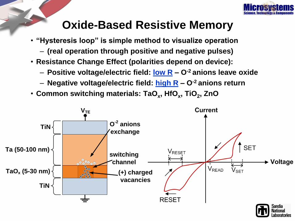
Oxide-Based Resistive Memory
• “Hysteresis loop” is simple method to visualize operation
– (real operation through positive and negative pulses)
• Resistance Change Effect (polarities depend on device):
– Positive voltage/electric field: low R – O-2 anions leave oxide
– Negative voltage/electric field: high R – O-2 anions return
• Common switching materials: TaOx, HfOx, TiO2, ZnO
TiN
Ta (50-100 nm)
TiN
TaOx (5-30 nm)
switching
channel
++
++
- ---
-
-
++
O-2
anions
exchange
VTE
(+) charged
vacancies+
+
++
+
--

Typical Device Fabrication
Si Substrate
1. Deposit Bottom Metal (Al)
2. Deposit USG
1
2
3. Etch via holes in USG
4. Deposit W and TiN layers
5. CMP
7. Etch bits
SiO2
Al Metal
USG
Si Substrate
3-5
SiO2
Al Metal
USG
0.35 – 0.5 µm bottom vias
W W
Si Substrate
SiO2
Al Metal
USGW W
Si Substrate
SiO2
Al Metal
USGW
TiN (20 nm)
TiN (20 nm)
6 Ta (15 nm)TaOx (10 nm)
6. Deposit bit stack (layers enlarged for clarity)
7
Si Substrate
SiO2
Al Metal
USGW
8-9
Si Substrate
SiO2
Al Metal
USGW
10
Al (700 nm)
10. Deposit top Al
0.35 – 1.5 µm top vias
0.75 – 1.5 µm bits
8. Deposit top USG
9. Etch top via holes in USG
W W
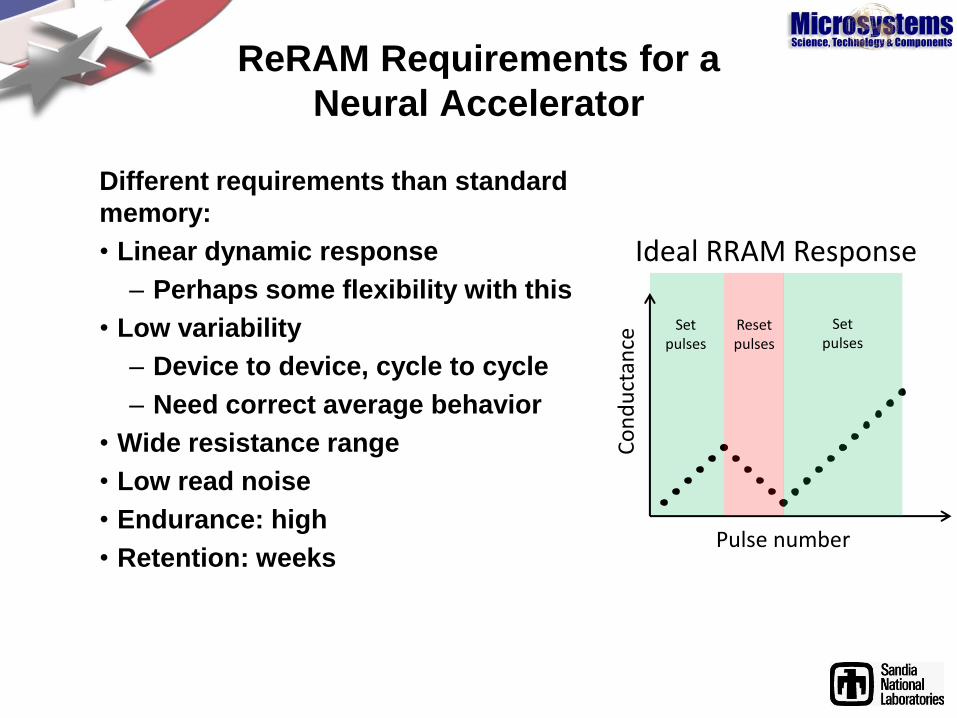
ReRAM Requirements for a
Neural Accelerator
Different requirements than standard
memory:
• Linear dynamic response
– Perhaps some flexibility with this
• Low variability
– Device to device, cycle to cycle
– Need correct average behavior
• Wide resistance range
• Low read noise
• Endurance: high
• Retention: weeks
Co
nd
uct
ance
Pulse number
Set pulses
Reset pulses
Set pulses
Ideal RRAM Response

Weight Updates with ReRAM
• Square pulse train of fixed amplitude and duration (typ. µs)
• Most common method of characterizing
• Do not want to erase many pulses with opposing pulse
Wang et al IEDM 2014 0 20 40 60 80 100 120 140 160
1.7m
1.8m
1.9m
2.0m
2.1m
Resistance
Co
nd
ucta
nce
(S
)
Pulse Number
-0.5
0.0
0.5 Pulse Height
Pu
lse
Heig
ht (V
)
Sandia TiN/TaOx/Ta/TiN ReRAM TaOx/TiO2 cell (IEDM 2014)

Variability and Noise
• Interdevice variability: device to device, can be >10x
– Variations in film thickness, topography
• Intradevice variability: cycle to cycle, can be >2x
– Fundamental physical attributes
• Random telegraph noise:
– Affects read current, usually least significant
2/25/2015
0.0 20.0k 40.0k 60.0k 80.0k 100.0k0
500
1000
1500
2000
2500
Resis
tan
ce
(
)
Cycle No.
ON
OFF
600.00 900.00 1200.00 1500.00 1800.000
20
40
60
80
100
CP
D (
%)
Off State Resistance (ROFF
) ()
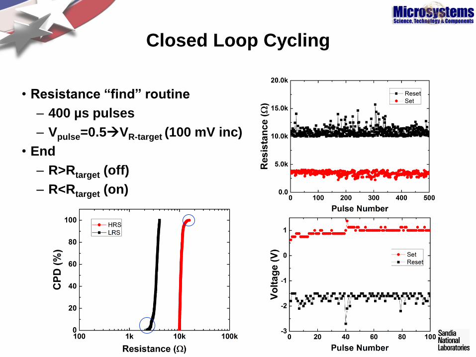
Closed Loop Cycling
• Resistance “find” routine
– 400 µs pulses
– Vpulse=0.5VR-target (100 mV inc)
• End
– R>Rtarget (off)
– R<Rtarget (on)

Open/Closed Loop Cycling
Open loop Vset=1V
Closed loop
Open loop Vreset = -2V
Closed loop
Closed
loop
Open
loop Vreset = -2V
Closed
loop
Open loop
Vset = 1V
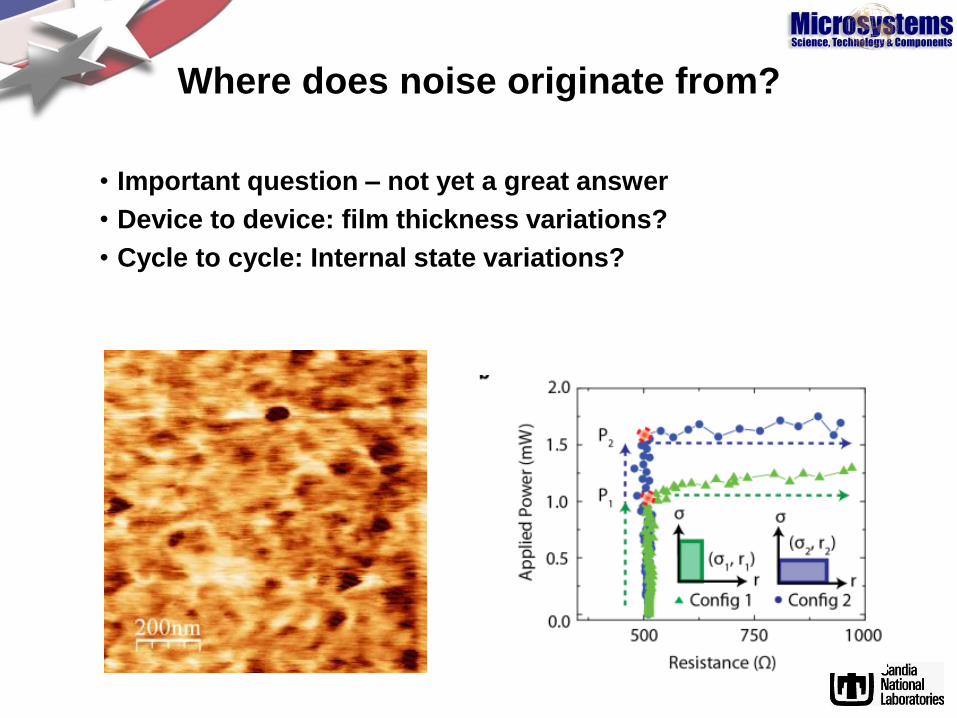
Where does noise originate from?
• Important question – not yet a great answer
• Device to device: film thickness variations?
• Cycle to cycle: Internal state variations?

How much noise can be tolerated?
• First step: Simulation Study
– Mimic on-line learning with incremental open-loop
resistance nudges
– Assume adjustment of each W by DW is done
imprecisely
– Add white noise to each weight update:
– Train on individual images or mini-batch or full epoch
– Train for fixed epoch count, or to convergence
– Adjust backprop step-size “a” if needed
– Classify as usual with final weights
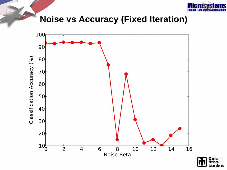
Noise vs Accuracy (Fixed Iteration)
• Motivation
• Neural Core Design and Architecture
• Resistive Memory Device Assessment
• Summary and Future Work
Outline
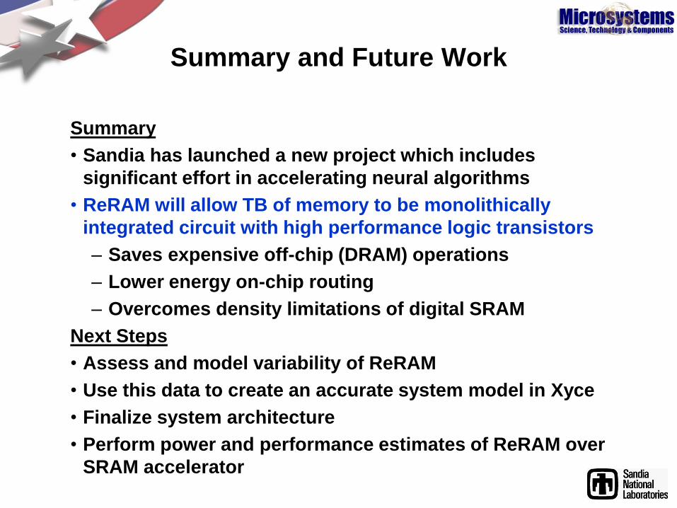
Summary and Future Work
Summary
• Sandia has launched a new project which includes
significant effort in accelerating neural algorithms
• ReRAM will allow TB of memory to be monolithically
integrated circuit with high performance logic transistors
– Saves expensive off-chip (DRAM) operations
– Lower energy on-chip routing
– Overcomes density limitations of digital SRAM
Next Steps
• Assess and model variability of ReRAM
• Use this data to create an accurate system model in Xyce
• Finalize system architecture
• Perform power and performance estimates of ReRAM over
SRAM accelerator

Acknowledgements
• This project was funded in part by Sandia’s
Laboratory Directed Research and Development
(LDRD) Program
• Collaborators: Stan Williams, Dick Henze, John-
Paul Strachan (HP), Jianhua Yang (U Mass),
Gennadi Bursuker (Sematech), Tarek Taha, Chris
Yakopcic (Dayton), et al.