residual stress control during the growth and release
TRANSCRIPT
Residual stress control during the growth and release process in gold suspended microstructures
Akshdeep Sharma*a, Deepak Bansala, Amit Kumara, Dinesh Kumarb, Kamaljit Rangraa
aSensors and Nanotechnology Group, Central Electronics Engineering Research Institute (CEERI)/
Council of Scientific and Industrial Research (CSIR), Pilani, Rajasthan, India, bDept. of Electronic Science, Kurukshetra University, Kurukshetra, Haryana, India,
ABSTRACT
This paper presents the growth and release process effects on the deformation of suspended gold micro-structures. Cantilever type test structures, typically used for RF MEMS devices have been examined. The structures have a thickness of 2µm, produced by patterned gold electro deposition above a sacrificial photoresist layer, then removed by dry release in oxygen plasma ashing and wet release using critical point dryer (CPD). The growth process of gold electroplating is optimized for low residual stress using pulse power supply. Minimum stress 35-60 MPa is obtained at grain size 30-45nm and RMS roughness of the order of 5-8nm. The growth mechanism of structural layer and releasing methods are optimized to obtain planar MEMS structures. The main parameters considered are the initial stress during the growth of electroplated gold and the release process recipes developed for fabrication of metallic structural layer.
Keywords: RF MEMS, Plasma ashing, Critical Point Dryer (CPD), Electroplating, Microstructure, Deformation
1. INTRODUCTION In view of the role of stress in MEMS (micro-electro-mechanical systems) device design, functioning and reliability, the identification and characterization of residual stress in MEMS structures is of paramount importance. From the device perspective, the existence of residual stresses1 essentially changes the performance and reduces the structural integrity and lifetime of MEMS devices. Therefore, in the MEMS device design one must predetermine and control the residual stress levels to obtain functional tolerances or to prevent total structural failure of a mechanical design. The existence of stress in thin film metallic structures used in most of the MEMS structures, leads to a change in effective stiffness, warping, local deformation or cracking of films in extreme cases. This severely undermines the device reliability and precision in terms of device parameters such as actuation voltage, s-parameters, natural mechanical frequency, and quality factor. On the other hand MEMS based techniques and devices provide a new tool for studying the mechanical properties of materials2 such as Young’s modulus, hardness, and state of stresses3. As a result, MEMS test structures4 have a very significant role in characterization of the mechanical properties (residual stress in particular) of MEMS devices and materials. In particular, stress and stress gradient are strongly dependent on deposition conditions, thermal treatments and other process dependent variables5.
In general, metals can be used in MEMS fabrication; gold is very attractive especially for RF MEMS devices, because of its high conductivity that helps reducing the losses, also for its chemical inertness that prevents contamination and corrosion problems. Gold is not an excellent material from the mechanical point of view, and its yield, creep and thermal relaxation properties are often source of high stresses and important homogeneities in the stress distribution. Electroplated gold thin films are commonly used for the MEMS devices as they provide a simple and cheap technology with superior material properties and device performances.
*[email protected] Phone 91 1596 252218; fax 91 1596 242294; www.ceeri.res.in
Micromachining and Microfabrication Process Technology XIX, edited by Mary Ann Maher, Paul J. Resnick,Proc. of SPIE Vol. 8973, 89730F · © 2014 SPIE · CCC code: 0277-786X/14/$18 · doi: 10.1117/12.2041433
Proc. of SPIE Vol. 8973 89730F-1
Downloaded From: http://proceedings.spiedigitallibrary.org/ on 03/13/2014 Terms of Use: http://spiedl.org/terms

Various MEMS devices such as pressure sensors, MEMS switches, microcoils, micromotors and microstructures based on plated metals have been fabricated and studied16-22. However, electroplated MEMS structures usually exhibit large deflections after the plasma ashing process, which is frequently used to release the MEMS structures from the substrate. The present study quantitatively analyses the electroplating growth mechanism and deformations of electroplated Au MEMS structures released by plasma ashing, CPD and investigate the possible causes of the deformations.
2. ORIGIN AND MEASUREMENT OF RESIDUAL STRESS 2.1 Thin film stress
The origin of stresses in thin films, microelectronics, and MEMS structures has been reviewed extensively by many researchers 1, 2. Fundamentally, it can be classified into two major categories, the mismatch between thermomechanical properties of materials and the thin-film deposition or growth generated intrinsic stress. Thermal stresses are induced due to strain misfits, as a result of differences in the temperature dependent coefficient of thermal expansion between the thin film and a substrate material such as silicon, photoresist, gold etc. Intrinsic stresses are generated due to strain misfits encountered during phase transformation in the formation of a solid layer of a thin film. Residual or internal thin film stress therefore can be defined as the summation of the thermal and intrinsic thin film stress components2
σ = σ + σ (1)
whereσ is the residual stress, σ is the thermal stress component, σ is the intrinsic stress component.
Simple mechanics of materials are therefore employed to study the mechanical residual stress induced in thin films. After a film is deposited onto a substrate at an elevated temperature, it cools down to a room temperature. When the film/substrate composite is cooled, they contract with different magnitudes because of different coefficients of thermal expansion between the film and the substrate. The film is subsequently strained elastically to match the substrate and remain attached, causing the substrate to bend. This along with the intrinsic film stress developed during film growth, gives rise to a total residual film stress 2-9.
2.2 Stress reduction during growth of layer
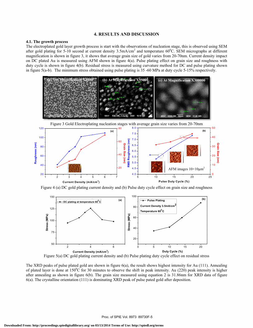
Residual stress control during the layer growth is an important process step. Growth mechanism strongly influences the in built stress. Electroplating process nucleation stages are shown in SEM micrographs in figures 3, from micrographs gold particle grain size range is measured from 20 -70nm.The stress measurement of the electrodeposit gold layer of 2µm thick is carried out using curvature measurement method as mentioned in next section. Initially electroplating is processed using DC power supply with varying current density and corresponding thickness, roughness, grain size and residual stress is measured. Same experiments are explored using pulse power supply; the purpose of the pulse supply is reducing the grain size and residual stress. The grain size and roughness is measured using AFM and XRD. 2.2.1 Grain Size measurement According to Scherer’s equation grain size can be measured using XRD data peak. The governing equations are as follows: Crystalline Size D = (2)
Microstrain ε = (3)
Estimation of number of crystallites N = (4)
Where λ: X-ray wavelength (1.54178Å), B is the full width at half maximum, θ Bragg’s angle, t film thickness and K constant average value (0.9). Figure 6(a) shows XRD peak for 2µm thick plated gold film after deposition and 6(b) shows after annealing at 1500C. XRD peak are used to find out grain size using equation 2 and crystalline orientation of Au deposit layer18. Grain sizes are further verified using AFM data. Finer grain size and reduced roughness deposit using
Proc. of SPIE Vol. 8973 89730F-2
Downloaded From: http://proceedings.spiedigitallibrary.org/ on 03/13/2014 Terms of Use: http://spiedl.org/terms

pulse power supply also measured using AFM and XRD as shown in figure 4 (b).The extracted parameters of electroplated gold for minimum residual stress, fine grain size and roughness are finalize. The resultant optimized plating recipes are used for fabricating single clamped cantilever structures as well as RF MEMS switches. 2.3 Stress measurements by substrate curvature method
The most widely acknowledged thin film stress measurement method is the curvature measurement of beam or plates structures. For beam structures, consider a composite film-substrate beam of width b. The film thickness and Young’s modulus are tf and Ef respectively, and the corresponding substrate values are ts and Es. In the free body diagram of each set of interfacial forces can be replaced by the statically equivalent combination of a force and moment Ff and Mf in the film, Fs and Ms in the substrate, where Ff = Fs. Force Ff can be imagined to act uniformly over the film cross section (tfb) giving rise to the film stress. The moments are responsible for the bowing of the film-substrate composite. By counting the biaxial state of stress and the final equation11 becomes
σ = = ( ) = ( ) ( ) (5)
Equation 5 is the standard Stoney’s formula to find out residual stress of the deposit layer, by measuring the radius of curvature (R) , before (Ri) and after (Rf) the thin film deposition on full wafer. The residual stress in the 2µm plated Au layer is between 100 -120MPa14. 2.4 Residual Stress Gradient measurement using cantilever The residual stresses of MEMS films usually vary in the thickness direction. A zero mean residual stress does not imply a satisfactory situation. Once the film is released by sacrificial etch, the mean residual stress vanish but the non-uniformity of the residual stress actually cause an out of plane deformation. As shown in figures 7, this out of plane deformation can cause performance degradation in MEMS devices such as RF switches. The uniformity of stress through the depth of a film introduces an important property to control. Variations in the magnitude and direction of the stress in the vertical direction can cause cantilever structures to curl toward or away from the substrate. Stress gradients present in MEMS films must be controlled to ensure predictable behavior of designed structures when released from the substrate12. To determine the residual stress, non-contact surface profilometer measurements for tip deflection is used on an array of simple cantilever beams. The stress gradient can be extracted from the deflection amplitude of different suspended cantilevers13. When the structure is released, the stress σ0 is relaxed and the stress gradient acts on the beam. The bending moment due to the stress gradient is written as:
M = zbσ(z)dz (6)
Where b is the beam width, and z the coordinate in the thickness direction. The stress gradient ′ is defined as σ′ = M/EI (7)
From beam theory for a cantilever with an applied end moment, the tip deflection due to the presence of the stress gradient is δtip = = (8) Eq. (9) shows the correlation of the tip deflection of the cantilever beam and the maximum stress on the beam cross-section24. σ = = (9) The displacement at the tip of the cantilever is measured with an optical profiler. The stress gradient 3.48×10⁻⁴µm-1 is extracted from the fit of the tip deflection versus the cantilever length14. Equation 9 is used to calculate maximum residual stress. The anchor effect24 is not considered in the equation 9.
Proc. of SPIE Vol. 8973 89730F-3
Downloaded From: http://proceedings.spiedigitallibrary.org/ on 03/13/2014 Terms of Use: http://spiedl.org/terms

Spacer layer photoresist HiPR 6517
P type <100> silicon wafer
(a) Deposit sacrificial layer photoresist
(b) Pattern Spacer layer photoresist
Photoresist AZ 9260
(d) Pattern photoresist mold and Au electroplating
(e) Remove the mold and seed layerr(c) Deposit seed layer (Au/Ti) for electroplating (f) Remove the spacer layer using plasma ashing and CPD
,
3. FABRICATION PROCESS STEPS Figure 1 shows the schematic view of process steps for MEMS cantilever as a part of RF MEMS switch fabrication16, 17. A set of microstructures were realized using surface micromachining techniques, on a 2″ diameter P-type <100> oriented silicon wafer. A thermal oxide was grown on the substrate, then a 3.5μm positive tone photoresist HiPR 6517 was deposited and patterned as a spacer layer. The main advantage of this PR is that after baking at 1800C, it becomes hard plastic like structure with edges suitable for conformal metal coating. A seed layer of Ti/Au is deposited by sputtering. This is followed by lithography of AZ 9260 photoresist for bridge mold formations. Gold electroplating of 2μm thick is obtained at current density 3.5mA/cm2 and temperature 600C for 10 minutes using sulphite gold (TSG 250) electrolyte. After the removal of PR mold and Au/Ti seed layers, microstructures are released by CPD and plasma ashing process. A layout of the cantilevers studied in this paper is reported in figure 2 (a-c), three cantilevers series with the same shape but with different dimensions (fig. 2 a, b and c). In the first cantilever series the length goes from 40 to 280µm and the width is 20µm while in the second cantilever series the length goes from 25 to 500 µm and the width is 30µm and in third cantilever series with actuation electrode length goes from 150-500µm and width is 30µm. The suspended parts are of gold color. The area originally covered by the spacer has been marked with a dashed line (gray color). These structures are representative of typical single-clamped microstructures encountered in MEMS fabrication. The devices have been distributed in several locations on the wafer layout to check the process uniformity on wafer.
Figure 1 (a)- (f) Fabrication process steps for electroplated MEMS cantilever
Figure2 (a) Narrow gold cantilever array (b) Large gold cantilever (c) Cantilever array with actuation electrode
Proc. of SPIE Vol. 8973 89730F-4
Downloaded From: http://proceedings.spiedigitallibrary.org/ on 03/13/2014 Terms of Use: http://spiedl.org/terms
J
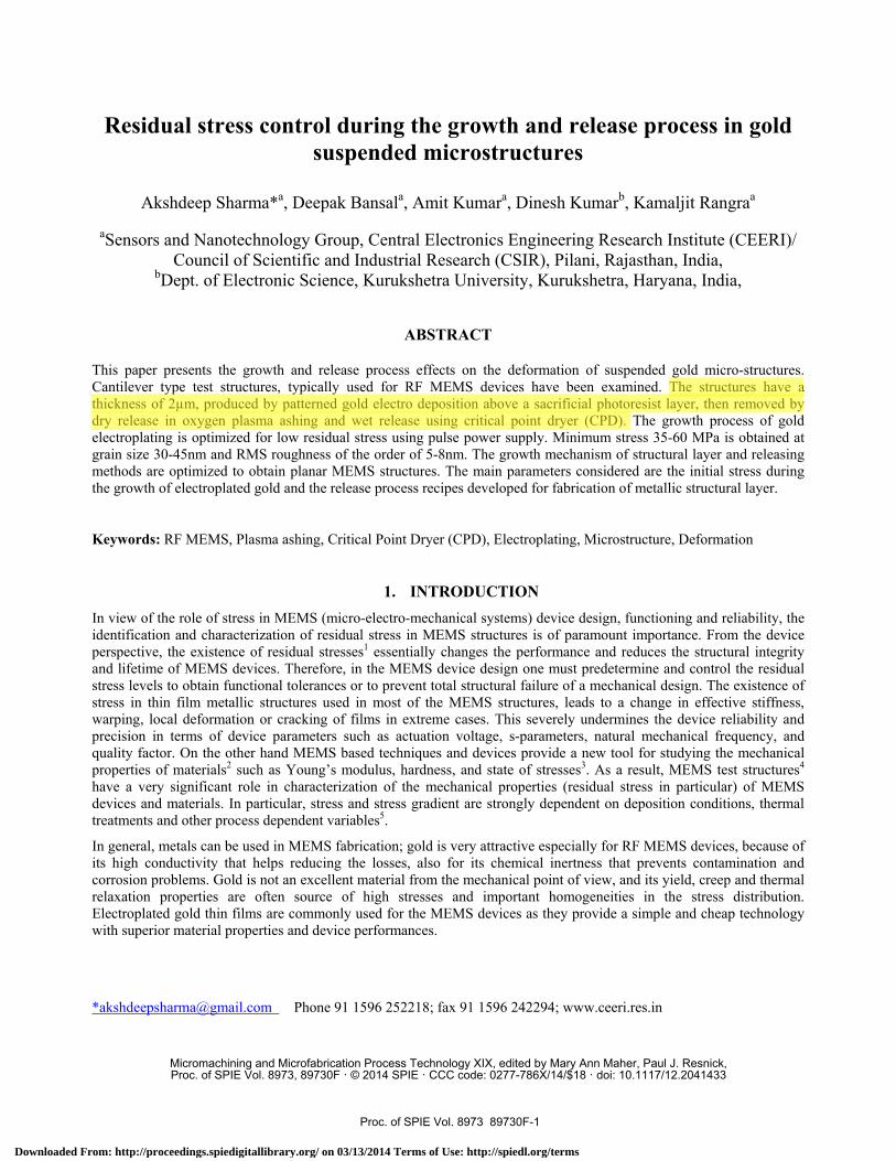
4.1. The growThe electroplafter gold plamagnificationon DC platedduty cycle is in figure 5(a-
120
40
60
80
100
120
Rou
ghne
ss (n
m)
Figu
Stre
ss(M
Pa)
Fig
The XRD peaof plated layeafter annealin6(a). The crys
(
wth process lated gold layeating for 5-10n is shown in d Au is measushown in figub). The minim
Figure 3 Go
2 3
Curre
ure 4 (a) DC g
250
75
100
125
150
Stre
ss (M
Pa)
DC pl
gure 5(a) DC
aks of pulse per is done at 1ng as shown istalline orient
(a) At Magnif
er growth proc0 second at cufigure 3, it shured using AFure 4(b). Resimum stress ob
old Electroplat
4 5
ent Density (mA/
gold plating cu
4
Current Densi
ating at temperatur
gold plating c
plated gold are1500C for 30 in figure 6(b)tation (111) is
fication X1400
4. RESULT
cess is start wurrent density
hows that averFM shown inidual stress is btained using p
ting nucleation
5 6
/cm2)
(a)
urrent density
6
ty (mA/cm2)
re 600C
current density
e shown in figminutes to ob
). The grain sidominating X
0 (b) At M
TS AND DIS
with the observy 3.5mA/cm2 rage grain sizen figure 4(a). P
measured usipulse plating
n stages with
7
20
40
60
80G
rain Size (nm)
and (b) Pulse
(a)
20
40
60
80
100
Stre
ss (M
Pa)
y and (b) Puls
gure 6(a), the rbserve the shiize measured
XRD peak of p
4.0
4.5
5.0
5.5
6.0
6.5
7.0
7.5
8.0R
MS
Rou
ghne
ss (n
m)
Magnification X
SCUSSION
vations of nucland temperatue of gold variePulse plating ing curvature is 35 -60 MPa
average grain
duty cycle ef
0 5
Pulse Pla
Current Densit
Temperature 6
e plating duty
result shows hift in peak inteusing equatio
pulse pated go
5 10
P
X95000 (
leation stage, ure 600C. SEMes from 20-70effect on gramethod for D
a at duty cycle
n size varies fr
ffect on grain s
10
Duty Cycle (%
ating
ty 3.5mA/cm2
600C
y cycle effect o
highest intensiensity. Au (22on 2 is 31.86nold after depos
15
Pulse Duty Cyc
(c) At Magnific
AFM im
this is observM micrograph
0nm. Current dain size and roDC and pulse e 5-15% respe
rom 20-70nm
size and rough
15 20
%)
(b
on residual str
ity for Au (1120) peak intennm for XRD sition.
20
le (%)
cation X300000
ages 10×10µm2
(b
ved using SEMhs at differendensity impacoughness withplating shown
ectively.
hness
b)
ress
11). Annealingnsity is higherdata of figure
250
10
20
30
40
50
Grain Size (nm
)
0
2
b)
M nt ct h n
g r e
Proc. of SPIE Vol. 8973 89730F-5
Downloaded From: http://proceedings.spiedigitallibrary.org/ on 03/13/2014 Terms of Use: http://spiedl.org/terms
30 40 50 60 70
0
200
400
600
800
1000
A u (220)
A u (200)
A u (111 ) (a)In
tens
ity (c
ount
s)
2θ (degree) 30 40 50 60 70
0
100
200
300
A u (200 )
A u (111)
A u (220 ) (b )
Inte
nsity
(cou
nts)
2θ (degree)
Figure 6(a, b) XRD patterns of plated Au film before and after annealing at a temperature of 1500C.
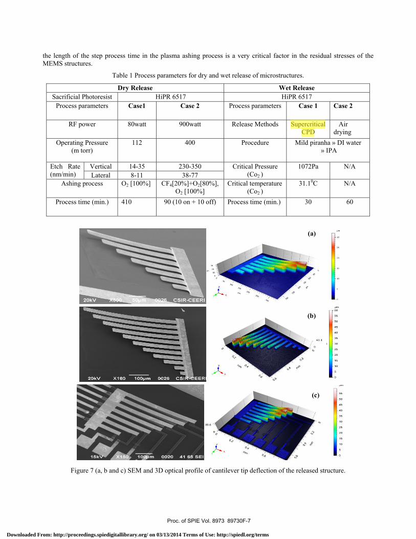
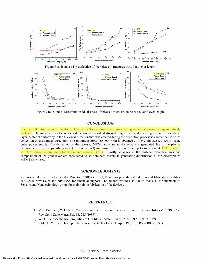
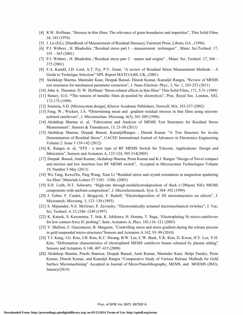
4.2. The release process The tip deflection of the released MEMS cantilever beam is measured after dry-etching the sacrificial layer with plasma ashing, and the residual stress is obtained based on the analytical model expressed in equation 9. The ‘Drytek mega strip 6 HF’ plasma asher which performs an isotropic dry etch of the PR with oxygen plasma, is used for dry release process. As the oxygen plasma (at 900watts) was inefficient in removing the hard crust of the PR baked at 1800C. For the crust removal, a combination of oxygen and CF4 was supplied to the plasma chamber in a ratio of 35:1, process details available in our publication25. Table 1 shows the recipes of the dry etching process used in the present study. To maintain the stable plasma etching condition, the minimum process time is experimentally determined as 10 min., after 3 min. in CF4 and O2 plasma for hard crust removal. The deformation characteristics with the etching condition of a single ashing process without break are excluded due to too large plastic deformation of the cantilever resulting damage of microstructure. Meanwhile, the residual stress causing the tip deflection of the MEMS structures can be generated not only in the plasma ashing process but also in the film deposition process. In order to evaluate the residual stress generated during the deposition process, the MEMS cantilever beam is released by removing the sacrificial layer with wet etching and the tip deflection is measured. The wet etching air dry and CPD release is also explored for cantilever structures in the present paper. Table 1 shows the recipe for wet etching process using CPD. Figure 7 (a-c) shows the SEM images of the released MEMS structures with 3D optical profiler images. 4.3 Tip deflection and the residual stress As shown in the figures 8 (a-c), the cantilever beams released by wet etching (CPD) shows small tip deflections while those released by plasma ashing show considerable amounts of tip deflections. The magnitude of the tip deflection of the cantilever beam released by plasma ashing seems to be dependent on the total process time as well as the step process time of plasma ashing. The detailed process time for each case is listed in Table 1. Table 1 shows two cases of plasma ashing and two cases of wet etching air and CPD. The plasma ashing consists of a case 1: O2 plasma at low RF power of 80 watt for total process time of 410 minutes, case 2: Initial CF4 + O2 plasma for hard crust removal, followed by O2 plasma step process time (10 min. on) and break time (10 min. off) at RF power 900watt for total process time 90 minutes. Plasma ashing case 1 has the long step process time in oxygen plasma; Case 2 has the short step process time as well as the short total process time. Case 1, with the long step process time, yields a larger deflection than in case 2 having the short step process time. Figures 8 shows the tip deflections of the MEMS cantilever beams of various lengths, where the tip deflections are measured by 3D optical profiler. The cantilever beams released by plasma ashing shows large deflections while those released by the wet etching CPD and air drying shows small deflections, regardless of the beam length. Wet release air drying structures have a problem of non-uniform deflection due to stiction to substrate, as this technique only suitable for high stiffness structures. Overall tip deflection of CPD released microstructures is 3-12µm as shown in figure 8 (a). Figure 9(a-c) shows the maximum residual stresses calculated from the measured tip deflections of the MEMS cantilever beams. The analytical model expressed in equation 9 is utilized to evaluate the maximum residual stresses24 and the value of Young’s modulus is set to 80 GPa and thickness 2µm of gold material. The residual stresses of the cantilever beams released by the CPD are small. Figure 9 also shows that case 1 has the highest residual stress, which confirms that
Proc. of SPIE Vol. 8973 89730F-6
Downloaded From: http://proceedings.spiedigitallibrary.org/ on 03/13/2014 Terms of Use: http://spiedl.org/terms
20kV X180 1001.i m 0026 CSI EER
o
20kV
o
fioSS
50
45
40
35
30
15
20
15
10
0
E. A 8: 9 A R R R:.
the length of the step process time in the plasma ashing process is a very critical factor in the residual stresses of the MEMS structures.
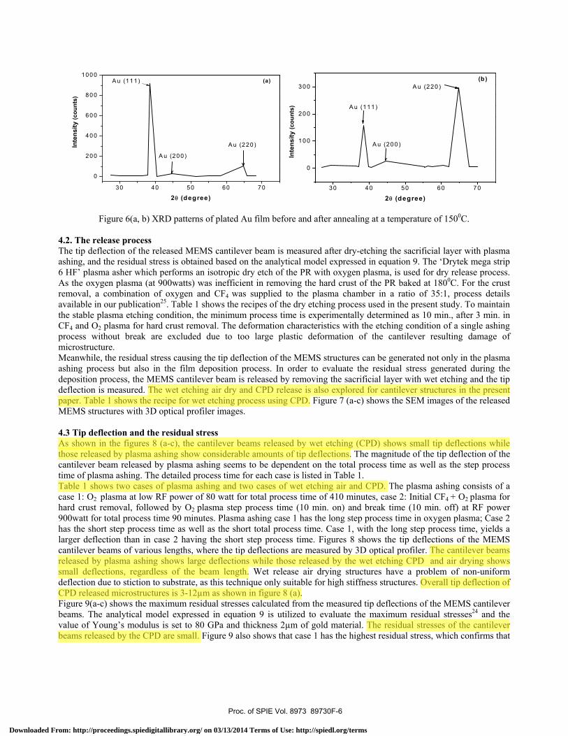
Table 1 Process parameters for dry and wet release of microstructures.
Figure 7 (a, b and c) SEM and 3D optical profile of cantilever tip deflection of the released structure.
Dry Release Wet Release Sacrificial Photoresist HiPR 6517 HiPR 6517
Process parameters Case1 Case 2 Process parameters Case 1 Case 2
RF power 80watt 900watt Release Methods Supercritical CPD
Air drying
Operating Pressure (m torr)
112 400 Procedure Mild piranha » DI water » IPA
Etch Rate (nm/min)
Vertical 14-35 230-350 Critical Pressure (Co2 )
1072Pa N/A Lateral 8-11 38-77
Ashing process O2 [100%]
CF4[20%]+O2[80%], O2 [100%]
Critical temperature (Co2 )
31.10C N/A
Process time (min.) 410 90 (10 on + 10 off) Process time (min.) 30 60
(a)
(b)
(c)
Proc. of SPIE Vol. 8973 89730F-7
Downloaded From: http://proceedings.spiedigitallibrary.org/ on 03/13/2014 Terms of Use: http://spiedl.org/terms
0 50 100 150 200 250 3000
5
10
15
20
25
30
35
Tip
Def
lect
ion
(μm
)
Cantilever Length (μm)
CPD Plasma Case 2 Plasma Case 1
(a)
0 100 200 300 400 5000
10
20
30
40
50
60
70(b)
Tip
Def
lect
ion
(μm
)
Cantilever Length (μm)
CPD Plasma Case 2 Plasma Case 1
100 150 200 250 300 350 400 450 500 5500
10
20
30
40
50
60
Tip
Def
lect
ion
(μm
)
Cantilever length (μm)
CPD Plasma Case 2 Plasma case 1
(c)
Figure 8 (a, b and c) Tip deflection of the released structures w.r.t. cantilever length.
0 50 100 150 200 250 300
0
200
400
600
800
1000
Max
imum
str
ess
(MPa
)
Cantilever Length (μm)
CPD Plasma Case 2 Plasma Case 1
(a)
0 100 200 300 400 500
0
500
1000
1500
2000
2500
Max
imum
Str
ess
(MPa
)
Cantilever Length (μm)
CPD Plasma Case 2 Plasma Case 1
(b)
100 200 300 400 5000
25
50
75
100
125
Max
imum
Str
ess
(MPa
)
Cantilever length (μm)
CPD Release Plasma Case 2 Plasma case 1
(c)
Figure 9 (a, b and c) Maximum residual stress of released microstructures w.r.t. cantilever length.
CONCLUSIONS The flexural deformation of the electroplated MEMS structures after plasma ashing and CPD released are quantitatively analysed. The main causes of cantilever deflection are residual stress during growth and releasing method of sacrificial layer. Material anisotropy in the thickness direction that was created during the deposition process is another cause of the deflection of the MEMS structures. The minimum stress (35- 60 MPa) is obtained at fine grain size (30-45nm) using pulse power supply. The deflection of the released MEMS structure in dry release is generated due to the plasma environment, small steps ashing time (10 min. on, off) minimise deformation effect up to some extent. CPD released structure shows minimum deformation and residual stress. Finally, changes in the surface microstructures and composition of the gold layer are considered to be dominant factors in generating deformation of the electroplated MEMS structures.
ACKNOWLEDGMENTS Authors would like to acknowledge Director, CSIR - CEERI, Pilani, for providing the design and fabrication facilities and CSIR New Delhi and NPMASS for financial support. The authors would also like to thank all the members of Sensors and Nanotechnology group for their help in fabrication of the devices.
REFERENCES
[1] M.F. Doerner , W.D. Nix , “Stresses and deformation processes in thin films on substrates” , CRC Crit. Rev. Solid State Mater. Sci. 14, 225 (1988)
[2] W.D. Nix, “Mechanical properties of thin films”, Metall. Trans. 20A, 2217 –2245 (1989) [3] S.M. Hu, “Stress related problems in silicon technology”, J. Appl. Phys. 70, R53– R80 ( 1991)
Proc. of SPIE Vol. 8973 89730F-8
Downloaded From: http://proceedings.spiedigitallibrary.org/ on 03/13/2014 Terms of Use: http://spiedl.org/terms
[4] R.W. Hoffman, “Stresses in thin films: The relevance of grain boundaries and impurities”, Thin Solid Films 34, 185 (1976)
[5] J. Lu (Ed.), [Handbook of Measurement of Residual Stresses], Fairmont Press ,Liburn, GA , (1996) [6] P.J. Withers , H. Bhadeshia ,“Residual stress part I – measurement techniques” , Mater. Sci.Technol. 17,
355 – 365 (2001) [7] P.J. Withers , H. Bhadeshia ,“Residual stress part 2 – nature and origins” , Mater. Sci. Technol. 17, 366 –
375 (2001) [8] F.A. Kandil, J.D. Lord, A.T. Fry, P.V. Grant, “A review of Residual Stress Measurement Methods – A
Guide to Technique Selection” NPL Report MATC(A)04, UK, (2001) [9] Akshdeep Sharma, Maninder Kaur, Deepak Bansal, Dinesh Kumar, Kamaljit Rangra, “Review of MEMS
test structures for mechanical parameter extraction”, J. Nano-Electron. Phys., 3, No. 1, 243-253 (2011) [10] John A. Thornton D. W. Hoffman “Stress-related effects in thin films” Thin Solid Films, 171, 5-31 (1989) [11] Stoney, G.G. “The tension of metallic films de-posited by electrolysis”, Proc. Royal Soc. London, A82,
172-175 (1999) [12] Senturia, S.D. [Microsystem design], Kluwer Academic Publishers, Norwell, MA, 183-237 (2002) [13] Fang, W.; Wickert, J.A. “Determining mean and gradient residual stresses in thin films using microm-
achined cantilevers”, J. Micromechan. Microeng. 6(3), 301-309 (1996) [14] Akshdeep Sharma et. al, “Fabrication and Analysis of MEMS Test Structures for Residual Stress
Measurement”, Sensors & Transducers, 13, 21-30 (2011) [15] Akshdeep Sharma, Deepak Bansal, KamaljitRangra , Dinesh Kumar “A Test Structure for in-situ
Determination of Residual Stress”, UACEE International Journal of Advances in Electronics Engineering Volume 2: Issue 3 139-142 (2012)
[16] K. Rangra et. al, “STS - a new type of RF MEMS Switch for Telecom. Applications: Design and fabrication”, Sensors and Actuators A, 123-124, 505-514(2005)
[17] Deepak Bansal, Amit Kumar, Akshdeep Sharma, Prem Kumar and K.J. Rangra “Design of Novel compact anti-stiction and low insertion loss RF MEMS switch”, Accepted in Microsystem Technologies Volume 19, Number 5 May (2013)
[18] Wu Tang, KeweiXu, Ping Wang, Xian Li “Residual stress and crystal orientation in magnetron sputtering Au films”,Materials Letters 57 3101– 3106, (2003)
[19] S.D. Leith, D.T. Schwartz, “High-rate through-moldelectrodeposition of thick (>200µm) NiFe MEMS components with uniform composition”, J. Microelectromech. Syst. 8, 384–392 (1999)
[20] J. Gobet, F. Cardot, J. Bergqvist, F. Rudolf, “Electrodeposition of 3D microstructures on silicon”, J. Micromech. Microeng. 3, 123–130 (1993)
[21] S. Majumder, N.E. McGruer, P. Zavracky, “Electrostatically actuated micromechanical switches”, J. Vac. Sci. Technol. A 15,1246–1249 (1997)
[22] K. Kataok, S. Kawamura, T. Itoh, K. Ishikawa, H. Honma, T. Suga, “Electroplating Ni micro-cantilevers for low contact-force IC probing”, Sens. Actuators A, Phys. 103,116–121 (2003)
[23] V. Mulloni, F. Giacomozzi, B. Margesin, ”Controlling stress and stress gradient during the release process in gold suspended micro-structures”Sensors and Actuators A 162, 93–99 (2010)
[24] T.J. Kang, J.G. Kim, J.H. Kim, K.C. Hwang, B.W. Lee, C.W. Baek, Y.K. Kim, D. Kwon, H.Y. Lee, Y.H. Kim, “Deformation characteristics of electroplated MEMS cantilever beams released by plasma ashing” Sensors and Actuators A 148, 407–415 (2008)
[25] Akshdeep Sharma, Prachi Jhanwar, Deepak Bansal, Amit Kumar, Maninder Kaur, Shilpi Pandey, Prem Kumar, Dinesh Kumar, and Kamaljit Rangra “Comparative Study of Various Release Methods for Gold Surface Micromachining” Accepted in Journal of Micro/Nanolithography, MEMS, and MOEMS (JM3), January(2014)
Proc. of SPIE Vol. 8973 89730F-9
Downloaded From: http://proceedings.spiedigitallibrary.org/ on 03/13/2014 Terms of Use: http://spiedl.org/terms