research update: behind the high efficiency of hybrid ... materials 4, 091505 (2016)...
TRANSCRIPT

Research Update: Behind the high efficiency of hybrid perovskite solar cellsAzhar Fakharuddin, Francesca De Rossi, Trystan M. Watson, Lukas Schmidt-Mende, and Rajan Jose Citation: APL Mater. 4, 091505 (2016); doi: 10.1063/1.4962143 View online: http://dx.doi.org/10.1063/1.4962143 View Table of Contents: http://scitation.aip.org/content/aip/journal/aplmater/4/9?ver=pdfcov Published by the AIP Publishing Articles you may be interested in Management of light absorption in extraordinary optical transmission based ultra-thin-film tandem solar cells J. Appl. Phys. 119, 193101 (2016); 10.1063/1.4949588 Molecular ferroelectric contributions to anomalous hysteresis in hybrid perovskite solar cells APL Mater. 2, 081506 (2014); 10.1063/1.4890246 Research Update: Physical and electrical characteristics of lead halide perovskites for solar cell applications APL Mater. 2, 040701 (2014); 10.1063/1.4871795 Hole-conductor-free perovskite organic lead iodide heterojunction thin-film solar cells: High efficiency andjunction property Appl. Phys. Lett. 104, 063901 (2014); 10.1063/1.4864638 Nanocrystalline metal electrodes for high-efficiency organic solar cells Appl. Phys. Lett. 85, 1832 (2004); 10.1063/1.1784879
Reuse of AIP Publishing content is subject to the terms at: https://publishing.aip.org/authors/rights-and-permissions. Download to IP: 183.171.170.60 On: Tue, 06 Sep
2016 22:08:00
APL MATERIALS 4, 091505 (2016)
Research Update: Behind the high efficiency of hybridperovskite solar cells
Azhar Fakharuddin,1,2,a Francesca De Rossi,3,a Trystan M. Watson,3Lukas Schmidt-Mende,1 and Rajan Jose4,a1Department of Physics, University of Konstanz, D-78457 Konstanz, Germany2School of Chemical and Materials Engineering, National University of Sciencesand Technology, H-12, Islamabad, Pakistan3College of Engineering, SPECIFIC – Swansea University, Bay Campus,SA1 8EN Swansea, United Kingdom4Nanostructured Renewable Energy Materials Laboratory, Universiti Malaysia Pahang,26300 Kuantan, Malaysia
(Received 15 July 2016; accepted 17 August 2016; published online 6 September 2016)
Perovskite solar cells (PSCs) marked tremendous progress in a short period oftime and offer bright hopes for cheap solar electricity. Despite high power conver-sion efficiency >20%, its poor operational stability as well as involvement oftoxic, volatile, and less-abundant materials hinders its practical deployment. Thefact that degradation and toxicity are typically observed in the most successfulperovskite involving organic cation and toxic lead, i.e., CH3NH3PbX3, requires adeep understanding of their role in photovoltaic performance in order to envisageif a non-toxic, stable yet highly efficient device is feasible. Towards this, wefirst provide an overview of the basic chemistry and physics of halide perov-skites and its correlation with its extraordinary properties such as crystal struc-ture, bandgap, ferroelectricity, and electronic transport. We then discuss devicerelated aspects such as the various device designs in PSCs and role of interfacesin origin of PV parameters particularly open circuit voltage, various film pro-cessing methods and their effect on morphology and characteristics of perovskitefilms, and the origin and elimination of hysteresis and operational stability in thesedevices. We then identify future perspectives for stable and efficient PSCs forpractical deployment. C 2016 Author(s). All article content, except where other-wise noted, is licensed under a Creative Commons Attribution (CC BY) license(http://creativecommons.org/licenses/by/4.0/). [http://dx.doi.org/10.1063/1.4962143]
I. INTRODUCTION
Solar cells made using organometallic halide perovskites (CH3NH3PbX3, where X = I, Cl andBr)—a next generation solution processable low cost material—have reached a certified powerconversion efficiency (PCE) ∼22.1%,1 in merely 4 yr since their first viable solid-state device in2012.2 In a typical perovskite solar cell (PSCs) architecture, a thin perovskite layer is stackedbetween an electron selective contact (ESC) and a hole selective contact (HSC) making a hetero-junction cell.3–7 The choice of selective contacts and the subsequent arrangement of the perovskitelayer determines device designs of PSCs ranging from mesoporous to a thin film like, conductingscaffolds based PSCs to electrically insulating ones, and also from bi-interfacial to single interfacialPSCs. All these devices showed a photoconversion efficiency ≥15% in a total active material thick-ness of <1 µm, thanks to the high absorption coefficient (103–104 cm−1) of CH3NH3PbX3 coupledwith its high charge carrier mobility (2–66 cm2 V−1 s−1).3,8
aAuthors to whom correspondence should be addressed. Electronic addresses: [email protected];[email protected]; and [email protected]
2166-532X/2016/4(9)/091505/16 4, 091505-1 ©Author(s) 2016.
Reuse of AIP Publishing content is subject to the terms at: https://publishing.aip.org/authors/rights-and-permissions. Download to IP: 183.171.170.60 On: Tue, 06 Sep
2016 22:08:00

091505-2 Fakharuddin et al. APL Mater. 4, 091505 (2016)
From a material perspective, the case of PSCs is very fascinating: the CH3NH3PbX3 has atunable bandgap ∼1.55 to 2.5 eV9,10 and can be processed from solutions at low temperatures<150 ◦C.11–14 The CH3NH3PbI3 perovskite undergoes rapid crystallization;15,16 therefore, a strictcontrol is often required for a desirable film morphology and properties thereby. High qualityfilms possess properties similar to that of inorganic semiconductors such as diffusion length of0.1–1.9 µm, low trap state density ∼1010 cm−3, and a carrier lifetime of ∼270 ns which coupledwith their low binding energy ≤5 meV makes them an ideal candidate for solar cells.17–19 However,the presence of lead (Pb) makes them toxic which accounts for ∼0.55% of total material,20 anamount slightly higher than the allowed limit set by European Restriction on Hazardous Substances.Furthermore, this material demonstrated ionic-electronic behavior leading to hysteresis in the de-vices,21–23 unless prepared with extreme care. In addition, these devices yet have to show a stableperformance comparable to that of silicon and thin film solar cells, primarily because the initialprecursors used to synthesize CH3NH3PbX3 are water soluble; and therefore, moisture sensitive.It is noteworthy that the hysteresis and stability of PSCs as well as their PV performance largelydepend on the preparation method, synthesis conditions as well as the selective contacts; therefore,efficient device fabrication requires appropriate knowledge of these various factors.
The main aim of this article is to provide insights into the contribution of various materialconstituents towards the PV performance in PSCs. Therefore, properties of CH3NH3PbX3 are corre-lated to its crystal structure in Sec. II. As the film processing and the device architecture largelyinfluence photovoltaic operation, we provide insights into the working mechanism of the variousPSC architectures, in particular, the role of a scaffold holding the perovskite crystals and the originof open circuit voltage in PSCs. Various film-processing methods are detailed followed by a discus-sion on the key issues that need to be solved for a commercially deployable device such as stabilityand hysteresis.
II. STRUCTURAL PROPERTIES OF HYBRID PEROVSKITES
Perovskite crystals are typically expressed by a general formula ABX3, where A and B are12-fold and 6-fold coordinated cations, respectively, and X is generally a halogen or oxygen.24,25
The 6-fold coordination of the B ion makes BX6 octahedra which are ideally corner shared along allthe three crystallographic axes (TiO6 and PbI6 octahedra in Figure 1) and the dodecahedral intersticethereby produced is filled by the A cation. To have the above structure, the ions forming it shouldhave a certain size distribution such that RA+RX√
2(RB+RX) = t, where the R′s are the Goldsmith ionicradius of the respective ions and the term t is referred as the tolerance factor, which is usually in the0.75–1 range, i.e., to tolerate a perovskite phase, the condition RA > RB > RX is always required.3
FIG. 1. Symmetric atomic positions of BaTiO3 (left) and MAPbI3 (right) in a perovskite lattice. The bond lengths are notoptimized. The arrows indicate the lattice translation vectors.
Reuse of AIP Publishing content is subject to the terms at: https://publishing.aip.org/authors/rights-and-permissions. Download to IP: 183.171.170.60 On: Tue, 06 Sep
2016 22:08:00
091505-3 Fakharuddin et al. APL Mater. 4, 091505 (2016)
The closer the tolerance factor is to unity, the more stable corner shared cubic perovskite forms forwhich RA ∼ 1.4 RB + 0.4 RX. Lower values of t lead to transition to lower crystal symmetries thancubic as well as the corner sharing octahedra changes to edge sharing and ultimately to face sharingoctahedra.26 In the case of non-ideal tolerance factor (t = 1), i.e., when the sizes of A, B, and X ionsdo not match well for a perfect octahedra, the BX6 octahedra undergoes a tilting and the A ion alsoconsequently displaced—which gives electrical polarity to perovskite crystals and is the source offerroelectricity in perovskite crystals. This octahedral tilting and subsequent phase transition are thesource of diverse range of electronic properties of perovskites.27
The inorganic oxide perovskites forms a large number of chemical entities such as A2+B4+ O2−
3 and A2+(B5+0.5B′3+0.5 )O2−
3 as one would find out elements to form a combination giving anacceptable tolerance factor and charge balance. However, the halide analogues do not offer thatenormity because (i) size of the halogen ions, excluding fluorine, is much higher than that ofoxygen—they demand larger ions to be at the centre of the octahedral and even larger ones at thedodecahedral positions, and (ii) halogen bears a single negative charge against two of the oxygen;therefore, A and B ions with a total valence of +3 only can give rise to an electrically neutral perov-skite. These size and charge requirements limits the halide perovskites to be realized from methy-lammonium ion (MA, RA ∼ 1.81 Å, charge +1), CS (RA ∼ 2.7 Å, charge +1), and formamidiniumion (FA, RA ∼ 2.79 Å, charge +1) for the A site;28 heavier group 14 elements such as Pb2+, Ge2+,Sn2+, alkaline earths, and bivalent rare-earth to be at its B site. A detailed account on the chemistryof formation of hybrid perovskite is published elsewhere.25 One would observe from their toler-ance factors that the organic/inorganic halides form perovskite structure with distorted octahedra(Table I); nature of their deviation and classification based on the octahedral tilting is summarized ina recent account.29 Consequently, existence of ferroelectric molecular domains in the methylammo-nium lead halide perovskite (MAPbX3) is predicted by ab initio molecular dynamic simulations.30
The difference in properties of the oxide perovskites, such as BaTiO3 (Figure 1(a)), and halideperovskite, such as MAPbX3 (Figure 1(b)), could be well understood from the difference in theirchemical structure as demonstrated in Figure 1.
The A site in the inorganic perovskite is occupied by a single atomic ion whereas it is occu-pied by a functional group (MA ion) in the hybrid phase. In addition, one would see that, by thevirtue of its symmetry, the MA ion is polar and would additionally contribute to the dielectricconstant offered by tilted of PI6 octahedra. The inorganic phase has a centre of symmetry; therefore,they do not possess certain optical properties such as photoluminescence. On the other hand, thehybrid phase is not a centrosymmetric crystal, thereby showing photoluminescence and extending
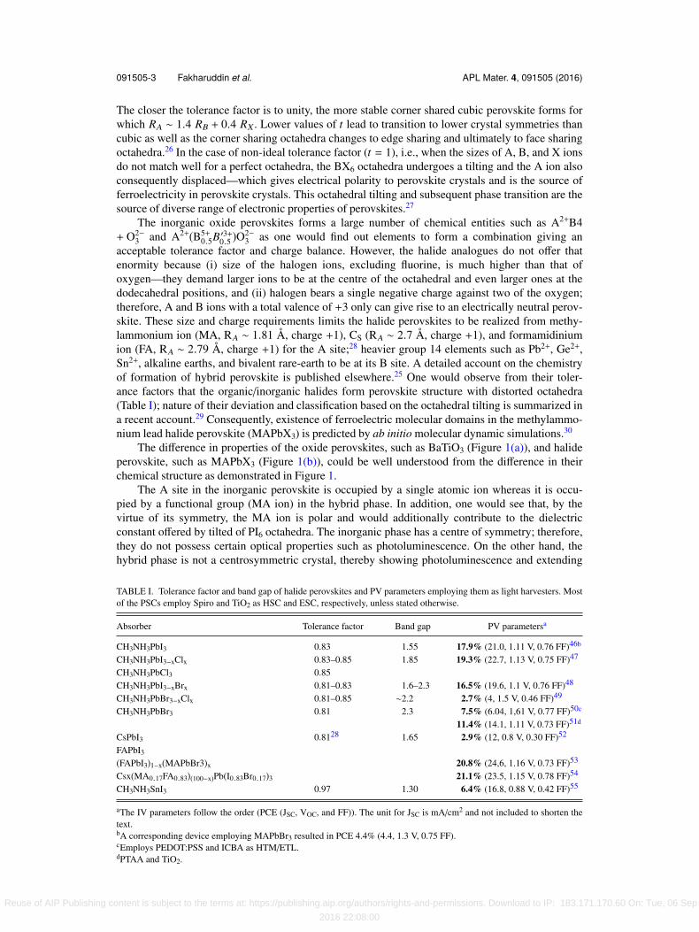
TABLE I. Tolerance factor and band gap of halide perovskites and PV parameters employing them as light harvesters. Mostof the PSCs employ Spiro and TiO2 as HSC and ESC, respectively, unless stated otherwise.
Absorber Tolerance factor Band gap PV parametersa
CH3NH3PbI3 0.83 1.55 17.9% (21.0, 1.11 V, 0.76 FF)46b
CH3NH3PbI3−xClx 0.83–0.85 1.85 19.3% (22.7, 1.13 V, 0.75 FF)47
CH3NH3PbCl3 0.85CH3NH3PbI3−xBrx 0.81–0.83 1.6–2.3 16.5% (19.6, 1.1 V, 0.76 FF)48
CH3NH3PbBr3−xClx 0.81–0.85 ∼2.2 2.7% (4, 1.5 V, 0.46 FF)49
CH3NH3PbBr3 0.81 2.3 7.5% (6.04, 1,61 V, 0.77 FF)50c
11.4% (14.1, 1.11 V, 0.73 FF)51d
CsPbI3 0.8128 1.65 2.9% (12, 0.8 V, 0.30 FF)52
FAPbI3
(FAPbI3)1−x(MAPbBr3)x 20.8% (24,6, 1.16 V, 0.73 FF)53
Csx(MA0.17FA0.83)(100−x)Pb(I0.83Br0.17)3 21.1% (23.5, 1.15 V, 0.78 FF)54
CH3NH3SnI3 0.97 1.30 6.4% (16.8, 0.88 V, 0.42 FF)55
aThe IV parameters follow the order (PCE (JSC, VOC, and FF)). The unit for JSC is mA/cm2 and not included to shorten thetext.bA corresponding device employing MAPbBr3 resulted in PCE 4.4% (4.4, 1.3 V, 0.75 FF).cEmploys PEDOT:PSS and ICBA as HTM/ETL.dPTAA and TiO2.
Reuse of AIP Publishing content is subject to the terms at: https://publishing.aip.org/authors/rights-and-permissions. Download to IP: 183.171.170.60 On: Tue, 06 Sep
2016 22:08:00

091505-4 Fakharuddin et al. APL Mater. 4, 091505 (2016)
optoelectronic functionalities to the perovskite crystals. Besides symmetry elements, motion of theA site ion also contributes to their optical non-linearities.31–33 Allowable motion of the ions in theinorganic phase is translatory, whereas the A site ion in the hybrid phase would additionally rotatein the presence of an electric field, magnetic field, or light. This peculiar geometry of the MAPbX3,that is a tilted PI6 octahedra with a polar entity at the A site, would offer changes in the total polarityof the crystal as the A-site ion is rotated—which is the source of the giant optical non-linearitiesof the MAPbX3 crystals. Consequently, there are considerable inconsistencies in the measureddielectric constant of the methylammonium lead halide perovskite. For instance, its static dielectricconstant is determined to be 6.5,34,35 70,36 and over 1000.37 A low temperature measurement underdark employing small perturbation condition is expected to provide accurate values.
The energy for molecular rotation is on the order of few meV, which thermal quanta at thenormal temperatures would provide; thereby offering significant challenges in precisely determin-ing the crystal structure parameters of hybrid perovskites. Considerable efforts have been devoted indetermining the crystal structure parameters of the MAPbX3 from X-ray diffraction measurementsand subsequent Rietveld refinement; however, the refined structure deviates considerably from theperovskite geometry, mainly the MA ion lacks a 12-fold symmetry in many of the refined struc-tures.8,38–40 Besides the inferior X-ray scatterability of light elements such as H, N, and C, accuratedetermination of the Debye-Waller instability also contributed to such inconsistency. One of thepotential remedies could be depending on diffraction by high energy radiations.41
A. Electronic properties of halide perovskites
As a solar cell material, emitting states of the MAPbX3 are extremely important. Consider-able attention is devoted to understand the electronic band structure of hybrid perovskites fromexperimental measurements and quantum chemical calculations.42–44 MAPbX3 is a direct band gapsemiconductor with two transitions at 760 and 480 nm. A general understanding is that top of thevalence band in both of these transitions are composed of p-orbitals of I mixed with 6p and 6sorbitals of Pb; the bottom of the conduction band is formed by σ-antibonding orbitals of 6p of Pband 5s of I and π-antibonding orbitals of 6p of Pb and 5p of I.24,45 No contribution from the MA ionhas been detected on the band edges and band gap, and their energy levels fall within the bands.
Now the significant question from a structural point of view of the halide perovskite is theorigin of photovoltaic action in PSCs. Low exciton binding energies (≤5 meV) of halide perovskitesdetermined experimentally from optical measurements36 and theoretically by DFT30 point out thatcharge generation is non-excitonic. Further, many experiments reveal the ionic character of thisperovskite.56,57 The mobile nature of the MA ion, its positive charge, and the fact that they arenot involved in the charge injection/dynamic states in the electronic bands of this crystal wouldhint that they provide an ion conducting pathway. The very low fill factor observed in the CsPbI3PSC (Table I) could be another supporting evidence for the role of the mobility of the A-site ionscontribution to the successful photovoltaic action. On the other hand, large electron density of leadand iodine, existence of ferroelectric molecular domains, and the fact that light absorption onlyinvolves the PbI6 octahedra would lead to think that they are the electron conducting pathway. Largedifference in PCE of the PSCs fabricated between MAPbI3 and CsPbI3 (Table I) would additionallyhint the role of the polar-and-mobile functional group entity at the A site rather than the relativelyfixed molecular ion (Cs) and their subsequent higher order optical susceptibility (non-linearity) onthe PV action.
III. DEVICE DESIGNS AND PHOTOVOLTAIC ACTION IN PEROVSKITE SOLAR CELLS
Historically, PSCs evolved from dye-sensitized solar cells (DSCs) where a dye is replaced witha perovskite absorber (CH3NH3PbI3 or CH3NH3PbBr3) of 15–20 times higher absorption coefficient(103–104 cm−1) on a mesoporous TiO2 film (∼10 µm) and resulted in PCE∼3.9%.58 Although thePCE was subsequently increased to 6.5% in a thinner TiO2 film (∼4 µm), the PSCs showed alifetime of few hours only, as the perovskite layer dissolved in the liquid electrolyte employed as ahole transport media.59
Reuse of AIP Publishing content is subject to the terms at: https://publishing.aip.org/authors/rights-and-permissions. Download to IP: 183.171.170.60 On: Tue, 06 Sep
2016 22:08:00
091505-5 Fakharuddin et al. APL Mater. 4, 091505 (2016)
A viable device is only shown when the liquid electrolyte is replaced by a solid-state HSC,e.g., 2,2′,7,7′-tetrakis-(N,N-p-dimethoxy-phenylamino)-9,9′-spirobifluorene (spiro-OMETAD) re-sulting in PCE∼9.7%.2 The higher absorption coefficient of CH3NH3PbX3 coupled with its highcharge carrier mobility (2–66 cm2 V−1 s−1)8 allowed TiO2 layer to be 300–500 nm, which togetherwith controlled perovskite crystallization further improved the performance up to ∼15%.15,60 Thestate-of-the-art performance in PSCs (19%-21%)46,53,54,61,62 is obtained by (i) chemically tailoringCH3NH3PbX3 by incorporating FA and/or Cs along with MA and also by introducing mixed halidesalts such as PbBr and PbI,54 (ii) optimized ESC and HSC for efficient charge extraction,47 and(iii) an optimized morphology of perovskite layer. Although high performance >20% is typicallyreported in devices employing a mesoporous scaffold (thickness∼150 to 300 nm), an excellentperformance 18%–19% is also reported in thin-film versions of PSCs47,63–65 employing a compactlayer as a selective contact.
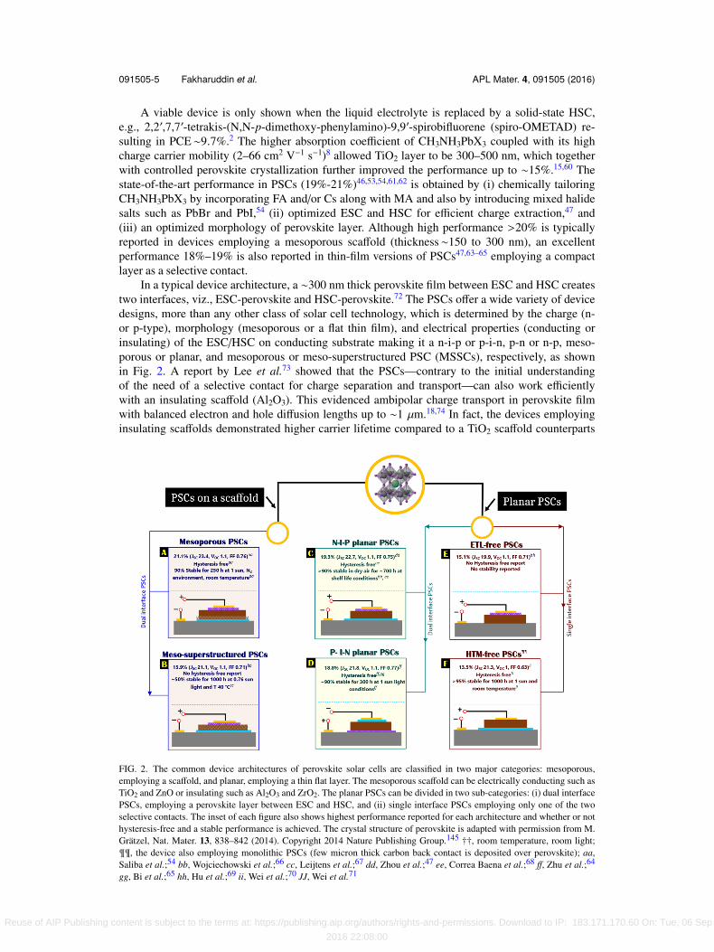
In a typical device architecture, a ∼300 nm thick perovskite film between ESC and HSC createstwo interfaces, viz., ESC-perovskite and HSC-perovskite.72 The PSCs offer a wide variety of devicedesigns, more than any other class of solar cell technology, which is determined by the charge (n-or p-type), morphology (mesoporous or a flat thin film), and electrical properties (conducting orinsulating) of the ESC/HSC on conducting substrate making it a n-i-p or p-i-n, p-n or n-p, meso-porous or planar, and mesoporous or meso-superstructured PSC (MSSCs), respectively, as shownin Fig. 2. A report by Lee et al.73 showed that the PSCs—contrary to the initial understandingof the need of a selective contact for charge separation and transport—can also work efficientlywith an insulating scaffold (Al2O3). This evidenced ambipolar charge transport in perovskite filmwith balanced electron and hole diffusion lengths up to ∼1 µm.18,74 In fact, the devices employinginsulating scaffolds demonstrated higher carrier lifetime compared to a TiO2 scaffold counterparts
FIG. 2. The common device architectures of perovskite solar cells are classified in two major categories: mesoporous,employing a scaffold, and planar, employing a thin flat layer. The mesoporous scaffold can be electrically conducting such asTiO2 and ZnO or insulating such as Al2O3 and ZrO2. The planar PSCs can be divided in two sub-categories: (i) dual interfacePSCs, employing a perovskite layer between ESC and HSC, and (ii) single interface PSCs employing only one of the twoselective contacts. The inset of each figure also shows highest performance reported for each architecture and whether or nothysteresis-free and a stable performance is achieved. The crystal structure of perovskite is adapted with permission from M.Grätzel, Nat. Mater. 13, 838–842 (2014). Copyright 2014 Nature Publishing Group.145 ††, room temperature, room light;¶¶, the device also employing monolithic PSCs (few micron thick carbon back contact is deposited over perovskite); aa,Saliba et al.;54 bb, Wojciechowski et al.;66 cc, Leijtens et al.;67 dd, Zhou et al.;47 ee, Correa Baena et al.;68 ff, Zhu et al.;64
gg, Bi et al.;65 hh, Hu et al.;69 ii, Wei et al.;70 JJ, Wei et al.71
Reuse of AIP Publishing content is subject to the terms at: https://publishing.aip.org/authors/rights-and-permissions. Download to IP: 183.171.170.60 On: Tue, 06 Sep
2016 22:08:00
091505-6 Fakharuddin et al. APL Mater. 4, 091505 (2016)
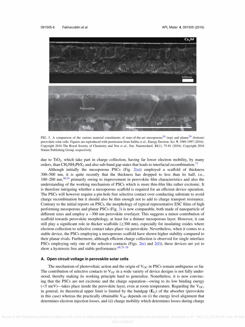
FIG. 3. A comparison of the various material constituents of state-of-the-art mesoporous54 (top) and planar79 (bottom)perovskite solar cells. Figures are reproduced with permission from Saliba et al., Energy Environ. Sci. 9, 1989-1997 (2016).Copyright 2016 The Royal Society of Chemistry and You et al., Nat. Nanotechnol. 11(1), 75-81 (2016). Copyright 2016Nature Publishing Group, respectively.
due to TiO2, which take part in charge collection, having far lower electron mobility, by manyorders, than CH3NH3PbX3 and also sub-band gap states that leads to interfacial recombination.73
Although initially the mesoporous PSCs (Fig. 2(a)) employed a scaffold of thickness300–500 nm, it is quite recently that the thickness has dropped to less than its half, i.e.,100–200 nm,46,54 primarily owing to improvement in perovskite film characteristics and also theunderstanding of the working mechanism of PSCs which is more thin-film like rather excitonic. Itis therefore intriguing whether a mesoporous scaffold is required for an efficient device operation.The PSCs will however require a pin-hole free selective contact over conducting substrate to avoidcharge recombination but it should also be thin enough not to add to charge transport resistance.Contrary to the initial reports on PSCs, the morphology of typical representative ESC films of highperforming mesoporous and planar PSCs (Fig. 3) is now comparable, both made of nanoparticle ofdifferent sizes and employ a ∼300 nm perovskite overlayer. This suggests a minor contribution ofscaffold towards perovskite morphology, at least for a thinner mesoporous layer. However, it canstill play a significant role in thicker scaffolds (≥300 nm), especially for insulating oxides whereelectron collection to selective contact takes place via perovskite. Nevertheless, when it comes to astable device, the PSCs employing a mesoporous scaffold have shown higher stability compared totheir planar rivals. Furthermore, although efficient charge collection is observed for single interfacePSCs employing only one of the selective contacts (Figs. 2(e) and 2(f)), these devices are yet toshow a hysteresis free and stable performance.69,75–78
A. Open circuit voltage in perovskite solar cells
The mechanism of photovoltaic action and the origin of VOC in PSCs remain ambiguous so far.The contribution of selective contacts to VOC in a wide variety of device designs is not fully under-stood, thereby making its working principle hard to generalize. Nonetheless, it is now convinc-ing that the PSCs are not excitonic and the charge separation—owing to its low binding energy(<5 meV)—takes place inside the perovskite layer, even at room temperature. Regarding the VOC,in general, its theoretical upper limit is limited by the bandgap (EG) of the absorber (perovskitein this case) whereas the practically obtainable VOC depends on (i) the energy level alignment thatdetermines electron injection losses, and (ii) charge mobility which determines losses during charge
Reuse of AIP Publishing content is subject to the terms at: https://publishing.aip.org/authors/rights-and-permissions. Download to IP: 183.171.170.60 On: Tue, 06 Sep
2016 22:08:00
091505-7 Fakharuddin et al. APL Mater. 4, 091505 (2016)
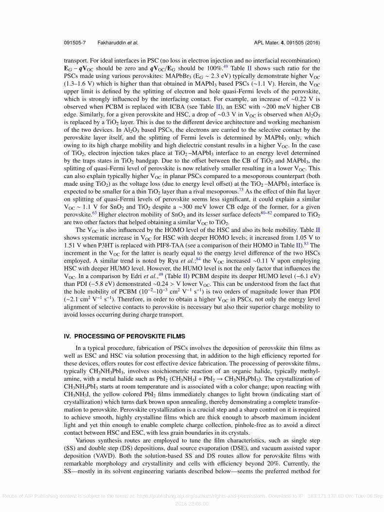
transport. For ideal interfaces in PSC (no loss in electron injection and no interfacial recombination)EG − qVOC should be zero and qVOC/EG should be 100%.49 Table II shows such ratio for thePSCs made using various perovskites: MAPbBr3 (EG ∼ 2.3 eV) typically demonstrate higher VOC(1.3–1.6 V) which is higher than that obtained in MAPbI3 based PSCs (∼1.1 V). Herein, the VOCupper limit is defined by the splitting of electron and hole quasi-Fermi levels of the perovskite,which is strongly influenced by the interfacing contact. For example, an increase of ∼0.22 V isobserved when PCBM is replaced with ICBA (see Table II), an ESC with ∼200 meV higher CBedge. Similarly, for a given perovskite and HSC, a drop of ∼0.3 V in VOC is observed when Al2O3is replaced by a TiO2 layer. This is due to the different device architecture and working mechanismof the two devices. In Al2O3 based PSCs, the electrons are carried to the selective contact by theperovskite layer itself, and the splitting of Fermi levels is determined by MAPbI3 only, whichowing to its high charge mobility and high dielectric constant results in a higher VOC. In the caseof TiO2, electron injection takes place at TiO2 –MAPbI3 interface to an energy level determinedby the traps states in TiO2 bandgap. Due to the offset between the CB of TiO2 and MAPbI3, thesplitting of quasi-Fermi level of perovskite is now relatively smaller resulting in a lower VOC. Thiscan also explain typically higher VOC in planar PSCs compared to a mesoporous counterpart (bothmade using TiO2) as the voltage loss (due to energy level offset) at the TiO2 –MAPbI3 interface isexpected to be smaller for a thin TiO2 layer than a rival mesoporous.73 As the effect of thin flat layeron splitting of quasi-Fermi levels of perovskite seems less significant, it could explain a similarVOC ∼ 1.1 V for SnO2 and TiO2 despite a ∼300 meV lower CB edge of the former, for a givenperovskite.63 Higher electron mobility of SnO2 and its lesser surface defects80–82 compared to TiO2are two other factors that helped obtaining a similar VOC to TiO2.
The VOC is also influenced by the HOMO level of the HSC and also its hole mobility. Table IIshows systematic increase in VOC for HSC with deeper HOMO levels; it increased from 1.05 V to1.51 V when P3HT is replaced with PIF8-TAA (see a comparison of their HOMO in Table II).83 Theincrement in the VOC for the latter is nearly equal to the energy level difference of the two HSCsemployed. A similar trend is noted by Ryu et al.;84 the VOC increased ∼0.11 V upon employingHSC with deeper HUMO level. However, the HUMO level is not the only factor that influences theVOC. In a comparison by Edri et al.,49 (Table II) PCBM despite its deeper HUMO level (−6.1 eV)than PDI (−5.8 eV) demonstrated ∼0.24 > V lower VOC. This can be understood from the fact thatthe hole mobility of PCBM (10−2–10−3 cm2 V−1 s−1) is two orders of magnitude lower than PDI(∼2.1 cm2 V−1 s−1). Therefore, in order to obtain a higher VOC in PSCs, not only the energy levelalignment of selective contacts to perovskite is necessary but also their superior charge mobility toavoid losses occurring during charge transport.
IV. PROCESSING OF PEROVSKITE FILMS
In a typical procedure, fabrication of PSCs involves the deposition of perovskite thin films aswell as ESC and HSC via solution processing that, in addition to the high efficiency reported forthese devices, offers routes for cost effective device fabrication. The processing of perovskite films,typically CH3NH3PbI3, involves stoichiometric reaction of an organic halide, typically methyl-amine, with a metal halide such as PbI2 (CH3NH3I + PbI2 → CH3NH3PbI3). The crystallization ofCH3NH3PbI3 starts at room temperature and is associated with a color change; upon reacting withCH3NH3I, the yellow colored PbI2 films immediately changes to light brown (indicating start ofcrystallization) which turns dark brown upon annealing, thereby demonstrating a complete transfor-mation to perovskite. Perovskite crystallization is a crucial step and a sharp control on it is requiredto achieve smooth, highly crystalline films which are thick enough to absorb maximum incidentlight and yet thin enough to enable complete charge collection, pinhole-free as to avoid a directcontact between HSC and ESC, with less grain boundaries in its crystals.
Various synthesis routes are employed to tune the film characteristics, such as single step(SS) and double step (DS) depositions, dual source evaporation (DSE), and vacuum assisted vapordeposition (VAVD). Both the solution-based SS and DS routes allow for perovskite films withremarkable morphology and crystallinity and cells with efficiency beyond 20%. Currently, theSS—mostly in its solvent engineering variants described below—seems the preferred method for
Reuse of AIP Publishing content is subject to the terms at: https://publishing.aip.org/authors/rights-and-permissions. Download to IP: 183.171.170.60 On: Tue, 06 Sep
2016 22:08:00
091505-8Fakharuddin
etal.APL
Mater.4,091505
(2016)
TABLE II. A comparison of state-of-the-art open circuit voltage obtained using various halide perovskites in conjunction with a diverse range of electron and hole selective contacts. The CB and VBedges for MAPbI3 and MAPbBr3 are (−3.9/−5.4) eV and (−3.4/−5.6) eV, respectively. ■, CB/conduction band edge of ESC; N, HUMO of HSC.
VOC
(V)JSC
(mA/cm2) FFPCE(%) ESC Device architecture HSC
Band edges(CB/HUMO)
Hole mobility(cm2 V−1 s−1) Device
qVOC/EG
(%)EG−qVOC
(eV) Reference
1.11 21.00 0.76 17.9 c,m-TiO2 Csx(MA0.17 FA0.83)(100x)Pb(I0.83Br0.17)3 Spiro-OMETAD −4.4■/−5.11N 10−3–10−4,85 MesoporousPSC
72 0.44 Saliba et al.54
1.13 22.7 0.75 19.3 Y-TiO2a CH3NH3 PbI3−xClx Spiro-OMETAD −5.11N 10−3–10−4,85 n-i-p planar 61 0.72 Zhou et al.47
1.00 1.14 0.40 0.5 TiO2 MAPbBr3 PDIb −5.8N 2.1 MSSC 48 1.201.30 1.08 0.40 0.6 Al2O3 MAPbBr3 PDIb −5.8N 2.1 56 1.00 Edri et al.86
1.29 6.60 0.70 5.9 TiO2 MAPbBr3 P-TAAc −5.14N >0.1,86 MesoporousPSC
56 1.01 Ryu et al.84
1.36 6.30 0.70 6.0 TiO2 MAPbBr3 PF8-TAAd −5.44N 4×10⁻³ 59 0.941.40 6.10 0.79 6.7 TiO2 MAPbBr3 PIF8-TAAe −5.51N 4×10⁻² 61 0.901.04 21.3 0.73 16.2 TiO2 MAPbI3 P-TAA −5.14N >0.1,86 67 0.510.92 8.90 0.56 4.6 TiO2 MAPbI3 PF8-TAA −5.44N 4×10⁻³ 59 0.631.04 19.0 0.46 9.1 TiO2 MAPbI3 PIF8-TAA −5.51N 4×10⁻² 67 0.511.50 4.00 0.47 2.7 Al2O3 MAPbBr3−xClx CBPf 6–6.2N87 MSSC 70 0.73 Edri et al.49
1.09 8.5 0.79 7.3 TiO2 MAPbBr3 P3HT −5.0N >0.1,86 MesoporousPSC
47 1.21 Heo et al.83
1.35 8.4 0.82 9.3 TiO2 MAPbBr3 P-TAA −5.14N 4×10⁻³ 59 0.951.51 8.4 0.82 10.4 TiO2 MAPbBr3 PIF8-TAA −5.51N 4×10⁻² 67 0.651.38 5.2 0.78 5.6 PCBMg MAPbBr3 PEDOT:PSS −3.9■/−5.3N p-i-n inverted 60 0.92 Wu et al.50
1.61 6.04 0.77 7.5 ICBAh MAPbBr3 PEDOT:PSS −3.7■/−5.3N 70 0.69 Wu et al.50
aY-TiO2: Yitrium doped TiO2.bPDI: N,N′-dialkyl perylenediimide.cP3HT: poly-(3-hexyl)thiophen.dP-TAA: oly[bis(4-phenyl) (2,4,6-trimethylphenyl)amine].ePIF8-TAA: poly-indenofl uoren-8-triarylamine.f CPB: 4,4′-bis(N-carbazolyl)-1,1′-biphenyl.gPCBM: phenyl-C61-butyric acid methyl ester.hICBA: 1′,1,4′,4′′-tetrahydro-di1,4methanonaphthaleno[1,2:2′,3′,56,60: 2′′,3′′]5,6 fullerene-C60.
Reuse of AIP Publishing content is subject to the terms at: https://publishing.aip.org/authors/rights-and-permissions. Download to IP: 183.171.170.60 On: Tue, 06 Sep 2016 22:08:00

091505-9 Fakharuddin et al. APL Mater. 4, 091505 (2016)
perovskite deposition at lab scale. Likely, it is also the more promising candidate to be employed infuture for large scale production, even if the primacy of one process or the other, in terms of cost andmanufacturing effectiveness, has not been systematically demonstrated yet.
A. Single step deposition
Single step (SS) deposition of perovskite films represents a low cost and facile route towardshigh-performance PSCs. The perovskite absorber is deposited starting from a solution of both PbX2and CH3NH3X (X: I, Cl, Br) in a polar solvent, like DMF,88 DMSO,48,89 γ-butyrolactone (GBL),90
or mixed solvents.91 Spin coating is the most widely employed technique at lab scale, but others,suitable for large areas, such as blade92,93 and slot die coating,94 have also been demonstrated.An annealing process is then required to evaporate the solvent and crystallize the perovskite. Itis typically carried out on a hot plate at 70-110 ◦C for several minutes up to few hours but canbe dramatically reduced to few seconds or even to 1 ms by NIR95 and photonic flash annealing,96
respectively, delivering in both cases around 11% PCE in alumina-based cells with mixed halideperovskite.
The mixed halide CH3NH3PbI3−xClx in a planar geometry has yielded 13.8% efficiency device1
when spin-coated from a DMF solution, without any additives nor interface engineering and ther-mally annealed with spiro-OMeTAD as HTM. This was further enhanced to 15.9% in cells with analumina scaffold66 and to 19.3% by modification/doping of both ITO and compact TiO2.47
Despite its simplicity, the key issue of SS deposition is the lack of control over the crystalli-zation process, being affected by many factors, from the choice of solvents90,91 and precursors tothe surface properties of the substrate,97,98 from the solvent evaporation during the deposition tothe annealing conditions.97,99 As a result, large morphological variations occur, leading to inhomo-geneous, rough, and partially covered layers, which reduce light absorption and increase the car-rier recombination rate, eventually causing a drop in both device efficiency and reproducibility.100
Optimizing the perovskite film coverage and morphology in SS method is then crucial and manystrategies have been reported so far, mainly to control the crystallization kinetics.
The use of additives to increase the solubility of the solid precursors in the solvent, suchas hydriodic acid (HI), enables the formation of dense, pinhole-free perovskite films with highcrystallinity, suppressing the formation of PbI2 impurities, detected otherwise in films without HI,and thereby reducing the traps. By adding a small amount of HI (100 µl/ml) to the MAPbI3 pre-cursor solution in DMF, an efficiency as high as 18.1% in planar perovskite solar cells, based onPEDOT:PSS and PCBM, has been achieved.101
Other solution additives, such as morphology controllers (e.g., NH4Cl,102,103 1,8-diiodooctane(DIO),104,105 and N-cyclohexyl-2-pyrrolidone (CHP)106) benefit the crystallization of perovskite,slowing it down and leading to uniform coverage and crystallization of perovskite films.
Modified SS methods, based on solvent engineering, such as solvent dripping/drop-casting48,107
and solvent-solvent extraction (or anti-solvent bath),108,109 have been shown to lead to fast andcontrolled crystallization of extremely uniform and dense perovskite films. The solvent drippingmethod involves a different solvent from the one in the precursor solution, dripped on top of the wetfilm during the spin coating process to induce a fast crystallization of uniformly sized grains. Xiaoet al.107 reported dripping chlorobenzene onto a spinning CH3NH3PbI3 film from a DMF solutiongiving rise to instantly flat, uniform layers, with large crystalline grains up to a micron in sizeyielding planar cells with PCE of over 13%. The second solvent rapidly reduces the solubility ofCH3NH3PbI3 in the mixed solvent and thereby promotes fast nucleation and growth of the crystalsin the film, whose formation is complete within 1 min. Furthermore, only 10 min of annealing at100 ◦C is needed to evaporate any residual solvent. For mesoporous cells, by Li-doping the TiO2 andusing mixed cations and halides in the precursor solution, PCE over 19% has been achieved.110
Similarly, by including in the precursor composition three different cations (Cs, MA, FA)and halides (Iodine, Bromine), a stabilized efficiency of 21.1% has been recently achieved viachlorobenzene dripping, followed by 1 h annealing at 100 ◦C, in cells with mesoporous TiO2 andspiro-OMeTAD as HTM.54 Zhu et al.64 report a remarkable 18.8% efficiency for p-i-n planar cells,endowed with toluene-dripped MAPI films.
Reuse of AIP Publishing content is subject to the terms at: https://publishing.aip.org/authors/rights-and-permissions. Download to IP: 183.171.170.60 On: Tue, 06 Sep
2016 22:08:00
091505-10 Fakharuddin et al. APL Mater. 4, 091505 (2016)
The solvent-solvent extraction108 avoids the thermal annealing step of the standard SS route byimmersing the perovskite film, immediately after the spin coating, in a bath of a low-boiling-point(anti) solvent, such as diethyl ether, at room temperature. The efficient extraction of the high-boiling-point solvent of the precursor solution, N-methyl-2-pyrrolidone (NMP), promotes rapid(within 2 min) crystallization of uniform, ultra-smooth, high quality perovskite films of controlledthicknesses. Zhou et al.108 reported a PCE up to 15.2% for planar CH3NH3PbI3 cells processed bythis method, which is potentially suitable for roll-to-roll manufacturing, once the spin coating isreplaced by other processes (spray, inkjet, and slot die).
The DSE60 can also be regarded as SS deposition: the organic source (MAI) and the inorganiccomponents (PbCl2) are evaporated simultaneously from separate sources at 10−5 mbar followed byannealing. The resulting CH3NH3PbI3−xClx films are extremely uniform and, incorporated in planarcells, show PCE of over 15%. Still the method is not easily scalable.
B. Double step deposition
The DS deposition of perovskite films in its first embodiment, introduced by Burschka15 formesoporous TiO2 cells, with 15% efficiency, comprised the deposition of PbI2 via spin coatingfollowed by immersion into a solution of CH3NH3I and drying at 70 ◦C for 30 min. PbI2 films con-verted instantaneously into CH3NH3PbI3, enabling much better control over the film morphologyand higher reproducibility than with standard SS deposition, as well as better pore filling and moreconformal capping layer.111 On the other hand, DS deposition presents some limitations such asadditional process steps, even if already demonstrated on large area via scalable slot-die coating androll-to-roll production,112 and comparatively higher processing cost than for SS.
Further optimization has led to efficiencies exceeding 20%, by introducing onto the TiO2 scaf-fold a mesoporous lead halide capping layer, which enables complete infiltration of the mixedcation solution resulting in rapid and full conversion to compact FA1−xMAxPb(I1−xBrx)3 films.113
Also for planar configuration, a nanostructured lead iodide layer facilitates the conversion toCH3NH3PbI3, leading to smooth and PbI2-free films with PCE of 16.21%. The immersion in MAIsolution can be substituted by a VAVD in presence of solid MAI, demonstrated also for largeareas,114 or by MAI spin coating, followed by annealing in the presence of DMF vapour.115
A very interesting and effective DS approach is the intermolecular exchange process (IEP),61
in which a mediator, i.e., DMSO, acts as both solvent and reactant for PbI2, to prevent rapid anduncontrolled self-assembly crystallization between MAI or FAI and PbI2. By spin coating a FAIsolution on top of DMSO-intercalated-PbI2 films, a direct molecular exchange of DMSO withFAI molecules occurs, producing large-grained FAPbI3 films without residual PbI2 and cells withefficiency greater than 20%.61
V. ISSUES IN PSCS—HYSTERESIS AND DEGRADATION OF PEROVSKITESOLAR CELLS
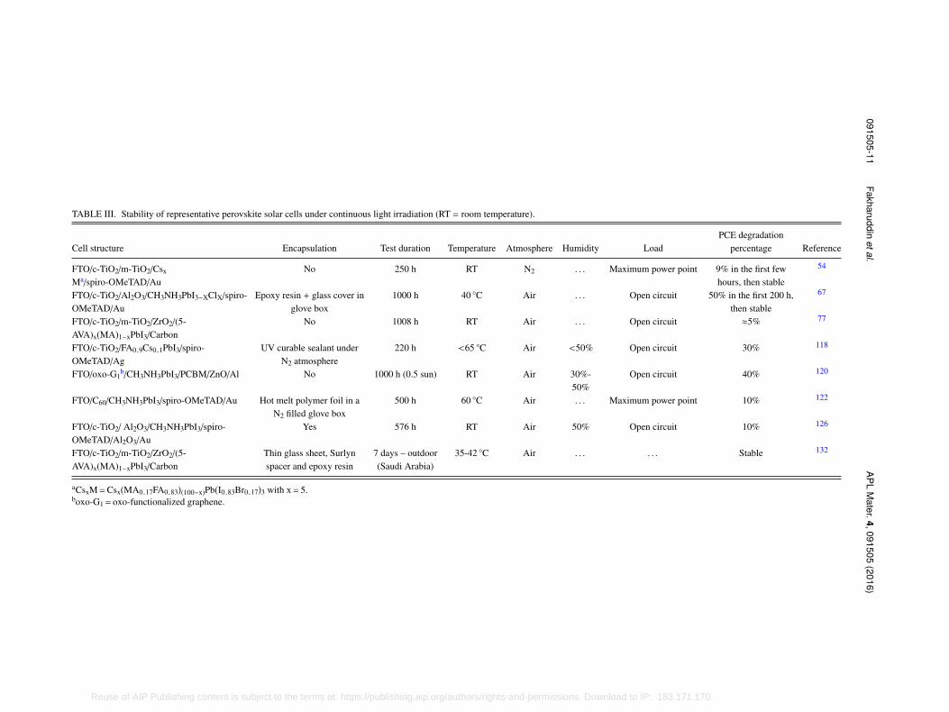
Despite the remarkable achievements in PCE of PSCs, one of the crucial issues prior toits commercial deployment is the stability of the device that depends on several factors, bothintrinsic, such as perovskite structural/chemical stability and extrinsic, i.e., moisture, oxygen, heat,light.116,117 This limits their lifetime to few hundreds of hours only, as shown in Table III. To startwith, the crystal structure of the perovskite should be intrinsically stable. CH3NH3PbX3 materialsare stable, both structurally and chemically, but still the hygroscopic nature of the organic cationcauses moisture ingress and thus degradation. Mixing or substituting the MA cation with FA orCs can improve the perovskite stability towards moisture and heat.54,118 A recent in situ FTIRspectroscopy study reveals that the evaporation of MA during the film fabrication itself triggers theinstability—hinting that the film fabrication is an important step for the stability of PSCs.119
Hysteresis, which is related to ionic motion in the perovskite and the nature of the contacts,can affect the photovoltaic characterization (i.e., variation in J-V curves for different scan rates) butit is unlikely detrimental in terms of device stability, even if it can worsen for devices stored/agedin air.116 Oxidation and photo-oxidation have been observed for perovskite thin films but are less
Reuse of AIP Publishing content is subject to the terms at: https://publishing.aip.org/authors/rights-and-permissions. Download to IP: 183.171.170.60 On: Tue, 06 Sep
2016 22:08:00
091505-11Fakharuddin
etal.APL
Mater.4,091505
(2016)
TABLE III. Stability of representative perovskite solar cells under continuous light irradiation (RT = room temperature).
Cell structure Encapsulation Test duration Temperature Atmosphere Humidity LoadPCE degradation
percentage Reference
FTO/c-TiO2/m-TiO2/Csx
Ma/spiro-OMeTAD/AuNo 250 h RT N2 . . . Maximum power point 9% in the first few
hours, then stable
54
FTO/c-TiO2/Al2O3/CH3NH3PbI3−XClX/spiro-OMeTAD/Au
Epoxy resin + glass cover inglove box
1000 h 40 ◦C Air . . . Open circuit 50% in the first 200 h,then stable
67
FTO/c-TiO2/m-TiO2/ZrO2/(5-AVA)x(MA)1−xPbI3/Carbon
No 1008 h RT Air . . . Open circuit ≈5% 77
FTO/c-TiO2/FA0.9Cs0.1PbI3/spiro-OMeTAD/Ag
UV curable sealant underN2 atmosphere
220 h <65 ◦C Air <50% Open circuit 30% 118
FTO/oxo-G1b/CH3NH3PbI3/PCBM/ZnO/Al No 1000 h (0.5 sun) RT Air 30%-
50%Open circuit 40% 120
FTO/C60/CH3NH3PbI3/spiro-OMeTAD/Au Hot melt polymer foil in aN2 filled glove box
500 h 60 ◦C Air . . . Maximum power point 10% 122
FTO/c-TiO2/ Al2O3/CH3NH3PbI3/spiro-OMeTAD/Al2O3/Au
Yes 576 h RT Air 50% Open circuit 10% 126
FTO/c-TiO2/m-TiO2/ZrO2/(5-AVA)x(MA)1−xPbI3/Carbon
Thin glass sheet, Surlynspacer and epoxy resin
7 days – outdoor(Saudi Arabia)
35-42 ◦C Air . . . . . . Stable 132
aCsxM=Csx(MA0.17FA0.83)(100−x)Pb(I0.83Br0.17)3 with x= 5.boxo-G1= oxo-functionalized graphene.
Reuse of AIP Publishing content is subject to the terms at: https://publishing.aip.org/authors/rights-and-permissions. Download to IP: 183.171.170.60 On: Tue, 06 Sep 2016 22:08:00

091505-12 Fakharuddin et al. APL Mater. 4, 091505 (2016)
severe in complete devices, depending on the hydrophobicity of the top layer120,121 and can beavoided by proper encapsulation under inert conditions, which enables cells to be stable for up to1000 h.67,73,122
Perovskite rapid degradation to water and even air moisture represents a huge concern. Thedegradation mechanism is a partially reversible hydration process, which leads to irreversible PbI2
formation after prolonged exposure to moisture.123 It can be dramatically accelerated by heat andelectric field, and also in presence of photodose,124,125 which confirms the need for effective encap-sulation and/or moisture resistant layers, such as buffer layers between perovskite and HTM,126,127
moisture-blocking HTMs,128 and hydrophobic carbon electrodes.77 In terms of photo-stability, UVlight seems to represent a threat for TiO2-based devices, through the surface adsorbed oxygen,which is desorbed under UV illumination, leaving behind trap sites acting as recombination cen-ters.67 Also, the perovskite layer is found to be reactive to anatase TiO2 nanoparticle scaffold ora flat counterpart that leads to ion migration across the interface129,130 whereas no degradation isobserved for TiO2 nanorods based devices130 that offer crystalline morphology and a thermodynam-ically stable rutile phase.114,131
On the other hand, TiO2-based devices show very rapid degradation in ambient conditions,induced by (white LED) light and oxygen,133 in particular by photogenerated superoxides causingdeprotonation of the methylammonium cation.134 The three-layered monolithic structure that doesinclude a TiO2 film represents an exception. Different reports demonstrate remarkable long-termstability for this architecture under different conditions, from simulated AM 1.5 sunlight77 to realoutdoor conditions.132 The thick carbon layer, a good oxygen absorber, likely provides an addi-tional supply of oxygen, it acts as a barrier and hosts a sort of “sacrificial” perovskite, infiltratedthroughout its thickness.116 Finally, planar heterojunction cells have been reported to be promisingfor long-term operation.101,122
As long as the materials are chosen carefully and the devices are properly encapsulated, theintrinsic and extrinsic factors of degradation could be overtaken. Additional efforts are needed tooptimize active materials, identify effective encapsulation strategies (that can be borrowed fromOPV or OLED technology), and define standard protocols for testing long-term stability so thatresults from a wide research community can be compared.
A. Hysteresis in perovskite solar cells
The J–V curves of PSCs typically show a dependency on the measurement conditions suchas scan direction, rate and range, and voltage pre-treatment.23,135 This often leads to difficulty inreporting true performance of the device as the PCE is overestimated when scanning from forward-to-reverse voltage sweep direction. The origin of this anomalous hysteresis is still under debate,the plausible cause being the ferroelectric properties of halide perovskites, their ionic-electronictransport, slow ion migration, dynamic trapping and de-trapping of photogenerated charges andalso due the charge accumulation at TiO2-perovskite interface.135–141 We refer to a comprehensivereview for further details on the origin of J–V hysteresis and its elimination.142 We also note itsstrong dependency on the ESC/HSC, device architecture, processing conditions of perovskite, andso forth. For example, replacement of TiO2 with PCBM or C60 as an ESC reduced hysteresis signifi-cantly.143,144 The fact that most high efficiency PSCs (both the planar and mesoporous) do not showany hysteresis points to the urgent need for optimizing the device architectures and interfacial layersand also the processing conditions, which would lead to efficient and stable PSCs.
VI. OUTLOOK
Solution processable perovskite solar cells of efficiency >20% provide much hope for a cleanenergy for planet Earth; however, few unsolved issues prevent them from practically deployed—most important of which is its challenging operational stability. To develop a stable device, onewould understand the origin of this instability, which in turn requires a clear understanding on themechanism of photovoltaic action in this device. A wide variety of available device architecture
Reuse of AIP Publishing content is subject to the terms at: https://publishing.aip.org/authors/rights-and-permissions. Download to IP: 183.171.170.60 On: Tue, 06 Sep
2016 22:08:00
091505-13 Fakharuddin et al. APL Mater. 4, 091505 (2016)
of perovskite solar cells could puzzle about the role of interfacial energetics towards origin ofPV parameters. For example, an understanding of literature shows that the open circuit voltagealthough is determined by the splitting of quasi-Fermi levels of perovskite, the extent of splittingis largely influenced by the interfacing selective contact. Furthermore, significant efforts have beenundertaken to discover and eliminate hysteresis in the current–voltage characteristics of the cellwhile measuring the photovoltaic parameters in the forward and the reverse bias conditions. Conse-quently, another “school of thought” that eliminating hysteresis would lead to stable device has alsobeen followed currently. Besides operational stability, perovskite solar cells have environmentaland economic drawbacks: crystal chemistry of hybrid perovskites requires toxic and less abundantmaterials (such as lead) for them to be photoactive. Could photoactive perovskites be synthesizedfrom less toxic and highly abundant materials? Also, the hybrid perovskites crystallized on insu-lating scaffolds also show high photoconversion efficiency in devices, giving further opportunityto optimize ideal crystals suitable choice of materials and synthesis methods. Thus, more in-depthanalysis will be necessary in future to see the full potential of perovskite solar cells and may alsogive us the possibility to design new materials with similar extraordinary properties.
ACKNOWLEDGMENTS
A.F. acknowledges Alexander von Humboldt Foundation for postdoctoral research fellowship.F.D.R. and T.M.W. would like to acknowledge the Welsh Assembly Government funded Sêr CymruSolar Project. R.J. acknowledges the Department of Research and Innovations of the UniversitiMalaysia Pahang for financial support.
1 NERL, Best research cell efficiencies, 2016.2 H. S. Kim, C. R. Lee, J. H. Im, K. B. Lee, T. Moehl, A. Marchioro, S. J. Moon, R. Humphry-Baker, J. H. Yum, J. E. Moser,
M. Grätzel, and N. G. Park, Sci Rep. 2, 591 (2012).3 M. A. Green, A. Ho-Baillie, and H. J. Snaith, Nat. Photonics 8(7), 506–514 (2014).4 H. Snaith and L. Schmidt-Mende, APL Mater. 2, 081201 (2014).5 P. Gao, M. Grätzel, and M. K. Nazeeruddin, Energy Environ. Sci. 7(8), 2448–2463 (2014).6 P. P. Boix, S. Agarwala, T. M. Koh, N. Mathews, and S. G. Mhaisalkar, J. Phys. Chem. Lett. 6(5), 898–907 (2015).7 H. S. Jung and N. G. Park, Small 11(1), 10–25 (2015).8 C. C. Stoumpos, C. D. Malliakas, and M. G. Kanatzidis, Inorg. Chem. 52, 9019–9038 (2013).9 Y. Yamada, T. Nakamura, M. Endo, A. Wakamiya, and Y. Kanemitsu, Appl. Phys. Express 7(3), 032302 (2014).
10 J. M. Ball, S. D. Stranks, M. T. Hörantner, S. Hüttner, W. Zhang, E. J. W. Crossland, I. Ramirez, M. Riede, M. B. Johnston,R. H. Friend, and H. J. Snaith, Energy Environ. Sci. 8(2), 602–609 (2015).
11 J. M. Ball, M. M. Lee, A. Hey, and H. J. Snaith, Energy Environ. Sci. 6(6), 1739–1743 (2013).12 B. Conings, L. Baeten, T. Jacobs, R. Dera, J. D’Haen, J. Manca, and H.-G. Boyen, APL Mater. 2, 081505 (2014).13 G. Xing, N. Mathews, S. S. Lim, N. Yantara, X. Liu, D. Sabba, M. Grätzel, S. Mhaisalkar, and T. C. Sum, Nat. Mater. 13,
476–480 (2014).14 F. Di Giacomo, A. Fakharuddin, R. Jose, and T. M. Brown, “Progress, challenges and perspectives in flexible perovskite
solar cells,” Energy Environ. Sci. (to be published).15 J. Burschka, N. Pellet, S. J. Moon, R. Humphry-Baker, P. Gao, M. K. Nazeeruddin, and M. Grätzel, Nature 499(7458),
316–319 (2013).16 T. Zhang, M. Yang, Y. Zhao, and K. Zhu, Nano Lett. 15(6), 3959–3963 (2015).17 M. Saba, M. Cadelano, D. Marongiu, F. Chen, V. Sarritzu, N. Sestu, C. Figus, M. Aresti, R. Piras, A. Geddo Lehmann, C.
Cannas, A. Musinu, F. Quochi, A. Mura, and G. Bongiovanni, Nat. Commun. 5, 5049 (2014).18 G. Xing, N. Mathews, S. Sun, S. S. Lim, Y. M. Lam, M. Gratzel, S. Mhaisalkar, and T. C. Sum, Science 342(6156), 344–347
(2013).19 S. Brittman, G. W. P. Adhyaksa, and E. C. Garnett, MRS Commun. 5(1), 7–26 (2015).20 L. Serrano-Lujan, N. Espinosa, T. T. Larsen-Olsen, J. Abad, A. Urbina, and F. C. Krebs, Adv. Energy Mater. 5(20), 1501119
(2015).21 R. S. Sanchez, V. Gonzalez-Pedro, J. W. Lee, N. G. Park, Y. S. Kang, I. Mora-Sero, and J. Bisquert, J. Phys. Chem. Lett.
5(13), 2357–2363 (2014).22 Y. Shao, Z. Xiao, C. Bi, Y. Yuan, and J. Huang, Nat. Commun. 5, 5784 (2014).23 H. J. Snaith, A. Abate, J. M. Ball, G. E. Eperon, T. Leijtens, N. K. Noel, S. D. Stranks, J. T. W. Wang, K. Wojciechowski,
and W. Zhang, J. Phys. Chem. Lett. 5(9), 1511–1515 (2014).24 F. Brivio, A. B. Walker, and A. Walsh, APL Mater. 1(4), 042111 (2013).25 B. Saparov and D. B. Mitzi, Chem. Rev. 116(7), 4558–4596 (2016).26 A. Glazer, Acta Crystallogr., Sect. B 28(11), 3384–3392 (1972).27 R. M. Hazen, Sci. Am. 258, 74 (1988).28 A. Amat, E. Mosconi, E. Ronca, C. Quarti, P. Umari, M. K. Nazeeruddin, M. Grätzel, and F. De Angelis, Nano Lett. 14(6),
3608–3616 (2014).
Reuse of AIP Publishing content is subject to the terms at: https://publishing.aip.org/authors/rights-and-permissions. Download to IP: 183.171.170.60 On: Tue, 06 Sep
2016 22:08:00

091505-14 Fakharuddin et al. APL Mater. 4, 091505 (2016)
29 C. C. Stoumpos and M. G. Kanatzidis, Acc. Chem. Res. 48, 2791–2802 (2015).30 J. M. Frost, K. T. Butler, and A. Walsh, APL Mater. 2, 081506 (2014).31 J. C. Johnson, Z. Li, P. F. Ndione, and K. Zhu, J. Mater. Chem. C 4(22), 4847–4852 (2016).32 B. S. Kalanoor, L. Gouda, R. Gottesman, S. Tirosh, E. Haltzi, A. Zaban, and Y. R. Tischler, ACS Photonics 3(3), 361–370
(2016).33 R. Zhang, J. Fan, X. Zhang, H. Yu, H. Zhang, Y. Mai, T. Xu, J. Wang, and H. J. Snaith, ACS Photonics 3(3), 371–377
(2016).34 M. Hirasawa, T. Ishihara, T. Goto, K. Uchida, and N. Miura, Physica B 201, 427–430 (1994).35 K. Tanaka, T. Takahashi, T. Ban, T. Kondo, K. Uchida, and N. Miura, Solid State Commun. 127(9-10), 619–623 (2003).36 Q. Lin, A. Armin, R. C. R. Nagiri, P. L. Burn, and P. Meredith, Nat. Photonics 9(2), 106–112 (2015).37 E. J. Juarez-Perez, R. S. Sanchez, L. Badia, G. Garcia-Belmonte, Y. Soo Kang, I. Mora-Sero, and J. Bisquert, J. Phys.
Chem. Lett. 5, 2390–2394 (2014).38 K. Liang, D. B. Mitzi, and M. T. Prikas, Chem. Mater. 10(1), 403–411 (1998).39 J. H. Im, J. Chung, S. J. Kim, and N. G. Park, Nanoscale Res. Lett. 7, 1–14 (2012).40 T. Baikie, Y. Fang, J. M. Kadro, M. Schreyer, F. Wei, S. G. Mhaisalkar, M. Graetzel, and T. J. White, J. Mater. Chem. A
1(18), 5628–5641 (2013).41 A. M. A. Leguy, J. M. Frost, A. P. McMahon, V. G. Sakai, W. Kochelmann, C. Law, X. Li, F. Foglia, A. Walsh, B. C.
O’Regan, J. Nelson, J. T. Cabral, and P. R. F. Barnes, Nat. Commun. 6, 7124 (2015).42 J. Even, L. Pedesseau, and C. Katan, J. Phys. Chem. C 118(22), 11566–11572 (2014).43 S. Zhao, C. Lan, J. Ma, S. S. Pandey, S. Hayase, and T. Ma, Solid State Commun. 213-214, 19–23 (2015).44 X. Zhu, H. Su, R. A. Marcus, and M. E. Michel-Beyerle, J. Phys. Chem. Lett. 5(17), 3061–3065 (2014).45 A. Buin, R. Comin, J. Xu, A. H. Ip, and E. H. Sargent, Chem. Mater. 27(12), 4405–4412 (2015).46 M. Saliba, S. Orlandi, T. Matsui, S. Aghazada, M. Cavazzini, J.-P. Correa-Baena, P. Gao, R. Scopelliti, E. Mosconi, K.-H.
Dahmen, F. De Angelis, A. Abate, A. Hagfeldt, G. Pozzi, M. Graetzel, and M. K. Nazeeruddin, Nat. Energy 1, 15017(2016).
47 H. Zhou, Q. Chen, G. Li, S. Luo, T. B. Song, H. S. Duan, Z. Hong, J. You, Y. Liu, and Y. Yang, Science 345(6196), 542–546(2014).
48 N. J. Jeon, J. H. Noh, Y. C. Kim, W. S. Yang, S. Ryu, and S. I. Seok, Nat. Mater. 13(9), 897–903 (2014).49 E. Edri, S. Kirmayer, M. Kulbak, G. Hodes, and D. Cahen, J. Phys. Chem. Lett. 5(3), 429–433 (2014).50 C. G. Wu, C. H. Chiang, and S. H. Chang, Nanoscale 8(7), 4077–4085 (2016).51 S. S. Mali, C. S. Shim, and C. K. Hong, NPG Asia Mater. 7, e208 (2015).52 G. E. Eperon, G. M. Paterno, R. J. Sutton, A. Zampetti, A. A. Haghighirad, F. Cacialli, and H. J. Snaith, J. Mater. Chem.
A 3(39), 19688–19695 (2015).53 D. Bi, W. Tress, M. I. Dar, P. Gao, J. Luo, C. Renevier, K. Schenk, A. Abate, F. Giordano, J.-P. Correa Baena, J.-D. Decoppet,
S. M. Zakeeruddin, M. K. Nazeeruddin, M. Grätzel, and A. Hagfeldt, Sci. Adv. 2(1), e1501170 (2016).54 M. Saliba, T. Matsui, J.-Y. Seo, K. Domanski, J.-P. Correa-Baena, M. K. Nazeeruddin, S. M. Zakeeruddin, W. Tress, A.
Abate, A. Hagfeldt, and M. Gratzel, Energ. Environ. Sci. 9, 1989–1997 (2016).55 N. K. Noel, S. D. Stranks, A. Abate, C. Wehrenfennig, S. Guarnera, A.-A. Haghighirad, A. Sadhanala, G. E. Eperon, S. K.
Pathak, M. B. Johnston, A. Petrozza, L. M. Herz, and H. J. Snaith, Energy Environ. Sci. 7(9), 3061–3068 (2014).56 D. Li, H. Wu, H.-C. Cheng, G. Wang, Y. Huang, and X. Duan, ACS Nano 10, 6933 (2016).57 C. Eames, J. M. Frost, P. R. F. Barnes, B. C. O’Regan, A. Walsh, and M. S. Islam, Nat. Commun. 6, 7497 (2015).58 A. Kojima, K. Teshima, Y. Shirai, and T. Miyasaka, J. Am. Chem. Soc. 131(17), 6050–6051 (2009).59 J. H. Im, C. R. Lee, J. W. Lee, S. W. Park, and N. G. Park, Nanoscale 3(10), 4088–4093 (2011).60 M. Liu, M. B. Johnston, and H. J. Snaith, Nature 501, 395–398 (2013).61 W. S. Yang, J. H. Noh, N. J. Jeon, Y. C. Kim, S. Ryu, J. Seo, and S. I. Seok, Science 348(6240), 1234–1237 (2015).62 N. Ahn, D. Y. Son, I. H. Jang, S. M. Kang, M. Choi, and N. G. Park, J. Am. Chem. Soc. 137(27), 8696–8699 (2015).63 M. Park, J.-Y. Kim, H. J. Son, C.-H. Lee, S. S. Jang, and M. J. Ko, Nano Energy 26, 208–215 (2016).64 Z. G. Zhu, Y. Bai, X. Liu, C.-C. Chueh, S. Yang, and A. K. Y. Jen, Adv. Mater. 28, 6478–6484 (2016).65 C. Bi, Q. Wang, Y. Shao, Y. Yuan, Z. Xiao, and J. Huang, Nat. Commun. 6, 7747 (2015).66 K. Wojciechowski, M. Saliba, T. Leijtens, A. Abate, and H. J. Snaith, Energy Environ. Sci. 7(3), 1142–1147 (2014).67 T. Leijtens, G. E. Eperon, S. Pathak, A. Abate, M. M. Lee, and H. J. Snaith, Nat. Commun. 4, 2885 (2013).68 J. P. Correa Baena, L. Steier, W. Tress, M. Saliba, S. Neutzner, T. Matsui, F. Giordano, T. J. Jacobsson, A. R. Srimath
Kandada, S. M. Zakeeruddin, A. Petrozza, A. Abate, M. K. Nazeeruddin, M. Gratzel, and A. Hagfeldt, Energy Environ.Sci. 8(10), 2928–2934 (2015).
69 Q. Hu, J. Wu, C. Jiang, T. Liu, X. Que, R. Zhu, and Q. Gong, ACS Nano 8(10), 10161–10167 (2014).70 H. Wei, J. Xiao, Y. Yang, S. Lv, J. Shi, X. Xu, J. Dong, Y. Luo, D. Li, and Q. Meng, Carbon 93, 861–868 (2015).71 Z. Wei, H. Chen, K. Yan, X. Zheng, and S. Yang, J. Mater. Chem. A 3(48), 24226–24231 (2015).72 V. Gonzalez-Pedro, E. J. Juarez-Perez, W.-S. Arsyad, E. M. Barea, F. Fabregat-Santiago, I. Mora-Sero, and J. Bisquert,
Nano Lett. 14, 888–893 (2014).73 M. M. Lee, J. Teuscher, T. Miyasaka, T. N. Murakami, and H. J. Snaith, Science 338(6107), 643–647 (2012).74 S. D. Stranks, G. E. Eperon, G. Grancini, C. Menelaou, M. J. P. Alcocer, T. Leijtens, L. M. Herz, A. Petrozza, and H. J.
Snaith, Science 342(6156), 341–344 (2013).75 D. Liu, J. Yang, and T. L. Kelly, J. Am. Chem. Soc. 136(49), 17116–17122 (2014).76 B. E. Cohen, S. Gamliel, and L. Etgar, APL Mater. 2(8), 081502 (2014).77 A. Mei, X. Li, L. Liu, Z. Ku, T. Liu, Y. Rong, M. Xu, M. Hu, J. Chen, Y. Yang, M. Gratzel, and H. Han, Science 345,
295–298 (2014).78 Y. Li, S. Ye, W. Sun, W. Yan, Y. Li, Z. Bian, Z. Liu, S. Wang, and C. Huang, J. Mater. Chem. A 3(36), 18389–18394 (2015).79 J. You, L. Meng, T. B. Song, T. F. Guo, W. H. Chang, Z. Hong, H. Chen, H. Zhou, Q. Chen, Y. Liu, N. De Marco, and Y.
Yang, Nat. Nanotechnol. 11(1), 75–81 (2016).
Reuse of AIP Publishing content is subject to the terms at: https://publishing.aip.org/authors/rights-and-permissions. Download to IP: 183.171.170.60 On: Tue, 06 Sep
2016 22:08:00

091505-15 Fakharuddin et al. APL Mater. 4, 091505 (2016)
80 Q. Wali, A. Fakharuddin, I. Ahmed, M. H. Ab Rahim, J. Ismail, and R. Jose, J. Mater. Chem. A 2(41), 17427–17434 (2014).81 Q. Wali, A. Fakharuddin, and R. Jose, J. Power Sources 293, 1039–1052 (2015).82 Q. Wali, A. Fakharuddin, A. Yasin, M. H. Ab Rahim, J. Ismail, and R. Jose, J. Alloys Compd. 646, 32–39 (2015).83 J. H. Heo, D. H. Song, and S. H. Im, Adv. Mater. 26(48), 8179–8183 (2014).84 S. Ryu, J. H. Noh, N. J. Jeon, Y. Chan Kim, W. S. Yang, J. Seo, and S. I. Seok, Energy Environ. Sci. 7(8), 2614–2618
(2014).85 W. H. Nguyen, C. D. Bailie, E. L. Unger, and M. D. McGehee, J. Am. Chem. Soc. 136(31), 10996–11001 (2014).86 E. Edri, S. Kirmayer, D. Cahen, and G. Hodes, J. Phys. Chem. Lett. 4(6), 897–902 (2013).87 M. Kröger, S. Hamwi, J. Meyer, T. Riedl, W. Kowalsky, and A. Kahn, Org. Electron. 10(5), 932–938 (2009).88 D. Shen, X. Yu, X. Cai, M. Peng, Y. Ma, X. Su, L. Xiao, and D. Zou, J. Mater. Chem. A 2(48), 20454–20461 (2014).89 B. Conings, L. Baeten, C. De Dobbelaere, J. D’Haen, J. Manca, and H. G. Boyen, Adv. Mater. 26(13), 2041–2046 (2014).90 J. Y. Jeng, Y. F. Chiang, M. H. Lee, S. R. Peng, T. F. Guo, P. Chen, and T. C. Wen, Adv. Mater. 25(27), 3727–3732 (2013).91 H. B. Kim, H. Choi, J. Jeong, S. Kim, B. Walker, S. Song, and J. Y. Kim, Nanoscale 6(12), 6679–6683 (2014).92 S. Razza, F. Di Giacomo, F. Matteocci, L. Cinà, A. L. Palma, S. Casaluci, P. Cameron, A. D’Epifanio, S. Licoccia, A. Reale,
T. M. Brown, and A. Di Carlo, J. Power Sources 277, 286 (2014).93 Z. Yang, C.-C. Chueh, F. Zuo, J. H. Kim, P.-W. Liang, and A. K. Y. Jen, Adv. Energy Mater. 5(13), 1500328 (2015).94 T. M. Schmidt, T. T. Larsen-Olsen, J. E. Carlé, D. Angmo, and F. C. Krebs, Adv. Energy Mater. 5(15), 1500569 (2015).95 J. Troughton, C. Charbonneau, M. J. Carnie, M. L. Davies, D. A. Worsley, and T. M. Watson, J. Mater. Chem. A 3(17),
9123–9127 (2015).96 J. Troughton, M. J. Carnie, M. L. Davies, C. Charbonneau, E. H. Jewell, D. A. Worsley, and T. M. Watson, J. Mater. Chem.
A 4(9), 3471–3476 (2016).97 G. E. Eperon, V. M. Burlakov, P. Docampo, A. Goriely, and H. J. Snaith, Adv. Func. Mater. 24(1), 151–157 (2014).98 S. Colella, E. Mosconi, P. Fedeli, A. Listorti, F. Gazza, F. Orlandi, P. Ferro, T. Besagni, A. Rizzo, G. Calestani, G. Gigli,
F. De Angelis, and R. Mosca, Chem. Mater. 25(22), 4613–4618 (2013).99 F. Wang, D. Meng, X. Li, Z. Zhu, Z. Fu, and Y. Lu, Appl. Surf. Sci. 357, 391–396 (2015).
100 J. H. Im, H. S. Kim, and N. G. Park, APL Mater. 2(8), 081510 (2014).101 J. H. Heo, H. J. Han, D. Kim, T. K. Ahn, and S. H. Im, Energy Environ. Sci. 8(5), 1602–1608 (2015).102 Y. Chen, Y. Zhao, and Z. Liang, Chem. Mater. 27(5), 1448–1451 (2015).103 C. Zuo and L. Ding, Nanoscale 6(17), 9935–9938 (2014).104 P. W. Liang, C. Y. Liao, C. C. Chueh, F. Zuo, S. T. Williams, X. K. Xin, J. Lin, and A. K. Y. Jen, Adv. Mater. 26(22),
3748–3754 (2014).105 C. C. Chueh, C. Y. Liao, F. Zuo, S. T. Williams, P. W. Liang, and A. K. Y. Jen, J. Mater. Chem. A 3(17), 9058–9062 (2015).106 Y. J. Jeon, S. Lee, R. Kang, J. E. Kim, J. S. Yeo, S. H. Lee, S. S. Kim, J. M. Yun, and D. Y. Kim, Sci. Rep. 4, 6953 (2014).107 M. Xiao, F. Huang, W. Huang, Y. Dkhissi, Y. Zhu, J. Etheridge, A. Gray-Weale, U. Bach, Y. B. Cheng, and L. Spiccia,
Angew. Chem., Int. Ed. 53(37), 9898–9903 (2014).108 Y. Zhou, M. Yang, W. Wu, A. L. Vasiliev, K. Zhu, and N. P. Padture, J. Mater. Chem. A 3(15), 8178–8184 (2015).109 Y. Zhou, M. Yang, O. S. Game, W. Wu, J. Kwun, M. A. Strauss, Y. Yan, J. Huang, K. Zhu, and N. P. Padture, ACS Appl.
Mater. Interfaces 8(3), 2232–2237 (2016).110 F. Giordano, A. Abate, J. P. Correa Baena, M. Saliba, T. Matsui, S. H. Im, S. M. Zakeeruddin, M. K. Nazeeruddin, A.
Hagfeldt, and M. Graetzel, Nat. Commun. 7, 10379 (2016).111 N. Yantara, D. Sabba, F. Yanan, J. M. Kadro, T. Moehl, P. P. Boix, S. Mhaisalkar, M. Grätzel, and C. Grätzel, Chem.
Commun. 51(22), 4603–4606 (2015).112 K. Hwang, Y. S. Jung, Y. J. Heo, F. H. Scholes, S. E. Watkins, J. Subbiah, D. J. Jones, D. Y. Kim, and D. Vak, Adv. Mater.
27(7), 1241–1247 (2015).113 C. Yi, X. Li, J. Luo, S. M. Zakeeruddin, and M. Grätzel, Adv. Mater. 28(15), 2964–2970 (2016).114 A. Fakharuddin, A. L. Palma, F. D. Giacomo, S. Casaluci, F. Matteocci, Q. Wali, M. Rauf, A. D. Carlo, T. M. Brown, and
R. Jose, Nanotechnology 26(49), 494002 (2015).115 Z. Xiao, Q. Dong, C. Bi, Y. Shao, Y. Yuan, and J. Huang, Adv. Mater. 26, 6503 (2014).116 T. Leijtens, G. E. Eperon, N. K. Noel, S. N. Habisreutinger, A. Petrozza, and H. J. Snaith, Adv. Energy Mater. 5(20),
1500963 (2015).117 T. A. Berhe, W. N. Su, C. H. Chen, C. J. Pan, J. H. Cheng, H. M. Chen, M. C. Tsai, L. Y. Chen, A. A. Dubale, and B. J.
Hwang, Energy Environ. Sci. 9(2), 323–356 (2016).118 J.-W. Lee, D.-H. Kim, H.-S. Kim, S.-W. Seo, S. M. Cho, and N.-G. Park, Adv. Energy Mater. 5(20), 1501310 (2015).119 C. Manspeaker, P. Scruggs, J. Preiss, D. A. Lyashenko, and A. A. Zakhidov, J. Phys. Chem. C 120(12), 6377–6382 (2016).120 H. Chen, Y. Hou, C. E. Halbig, S. Chen, H. Zhang, N. Li, F. Guo, X. Tang, N. Gasparini, I. Levchuk, S. Kahmann, C. O.
Ramirez Quiroz, A. Osvet, S. Eigler, and C. J. Brabec, J. Mater. Chem. A 4, 11604 (2016).121 L. Zheng, Y. H. Chung, Y. Ma, L. Zhang, L. Xiao, Z. Chen, S. Wang, B. Qu, and Q. Gong, Chem. Commun. 50(76),
11196–11199 (2014).122 K. Wojciechowski, T. Leijtens, S. Spirova, C. Schlueter, M. Hoerantner, J. T.-W. Wang, C.-Z. Li, A. K.-Y. Jen, T.-L. Lee,
and H. J. Snaith, J. Phys. Chem. Lett. 6, 2399–2405 (2015).123 A. Leguy, Y. Hu, M. Campoy-Quiles, M. I. Alonso, O. J. Weber, P. Azarhoosh, M. van Schilfgaarde, M. T. Weller, T. Bein,
J. Nelson, P. Docampo, and P. R. F. Barnes, Chem. Mater. 27(9), 3397–3407 (2015).124 F. Matsumoto, S. M. Vorpahl, J. Q. Banks, E. Sengupta, and D. S. Ginger, J. Phys. Chem. C 119(36), 20810–20816 (2015).125 N. A. Manshor, Q. Wali, K. K. Wong, S. K. Muzakir, A. Fakharuddin, L. Schmidt-Mende, and R. Jose, Phys. Chem. Chem.
Phys. 18, 21629 (2016).126 S. Guarnera, A. Abate, W. Zhang, J. M. Foster, G. Richardson, A. Petrozza, and H. J. Snaith, J. Phys. Chem. Lett. 6(3),
432–437 (2015).127 X. Dong, X. Fang, M. Lv, B. Lin, S. Zhang, J. Ding, and N. Yuan, J. Mater. Chem. A 3(10), 5360–5367 (2015).
Reuse of AIP Publishing content is subject to the terms at: https://publishing.aip.org/authors/rights-and-permissions. Download to IP: 183.171.170.60 On: Tue, 06 Sep
2016 22:08:00

091505-16 Fakharuddin et al. APL Mater. 4, 091505 (2016)
128 S. N. Habisreutinger, T. Leijtens, G. E. Eperon, S. D. Stranks, R. J. Nicholas, and H. J. Snaith, Nano Lett. 14(10), 5561–5568(2014).
129 A. Fakharuddin, F. Di Giacomo, I. Ahmed, Q. Wali, T. M. Brown, and R. Jose, J. Power Sources 283, 61–67 (2015).130 A. Fakharuddin, F. Di Giacomo, A. L. Palma, F. Matteocci, I. Ahmed, S. Razza, A. D’Epifanio, S. Licoccia, J. Ismail, A.
Di Carlo, T. M. Brown, and R. Jose, ACS Nano 9(8), 8420–8429 (2015).131 I. Ahmed, A. Fakharuddin, Q. Wali, A. R. B. Zainun, J. Ismail, and R. Jose, Nanotechnology 26(10), 105401 (2015).132 X. Li, M. Tschumi, H. Han, S. S. Babkair, R. A. Alzubaydi, A. A. Ansari, S. S. Habib, M. K. Nazeeruddin, S. M. Zakeerud-
din, and M. Grätzel, Energy Technol. 3, 551–555 (2015).133 D. Bryant, N. Aristidou, S. Pont, I. Sanchez-Molina, T. Chotchunangatchaval, S. Wheeler, J. R. Durrant, and S. A. Haque,
Energy Environ. Sci. 9(5), 1655–1660 (2016).134 N. Aristidou, I. Sanchez-Molina, T. Chotchuangchutchaval, M. Brown, L. Martinez, T. Rath, and S. A. Haque, Angew.
Chem., Int. Ed. 54, 8208–8212 (2015).135 E. L. Unger, E. T. Hoke, C. D. Bailie, W. H. Nguyen, A. R. Bowring, T. Heumüller, M. G. Christoforod, and M. D. McGehee,
Energy Environ. Sci. 7, 3690–3698 (2014).136 J. Wei, Y. Zhao, H. Li, G. Li, J. Pan, D. Xu, Q. Zhao, and D. Yu, J. Phys. Chem. Lett. 5, 3937–3945 (2014).137 H.-W. Chen, N. Sakai, M. Ikegami, and T. Miyasaka, J. Phys. Chem. Lett. 6, 164–169 (2015).138 A. Dualeh, T. Moehl, N. Tétreault, J. Teuscher, P. Gao, M. K. Nazeeruddin, and M. Grätzel, ACS Nano 8, 362–373 (2014).139 Y. Yang, J. Xiao, H. Wei, L. Zhu, D. Li, Y. Luo, H. Wu, and Q. Meng, RSC Adv. 4(95), 52825–52830 (2014).140 O. Almora, I. Zarazua, E. Mas-Marza, I. Mora-Sero, J. Bisquert, and G. Garcia-Belmonte, J. Phys. Chem. Lett. 6, 1645–1652
(2015).141 B. Chen, M. Yang, X. Zheng, C. Wu, W. Li, Y. Yan, J. Bisquert, G. Garcia-Belmonte, K. Zhu, and S. Priya, J. Phys. Chem.
Lett. 6, 4693–4700 (2015).142 B. Chen, M. Yang, S. Priya, and K. Zhu, J. Phys. Chem. Lett. 7(5), 905–917 (2016).143 K. Wojciechowski, S. D. Stranks, A. Abate, G. Sadoughi, A. Sadhanala, N. Kopidakis, G. Rumbles, C.-Z. Li, R. H. Friend,
A. K.-Y. Jen, and H. J. Snaith, ACS Nano 8, 12701–12709 (2014).144 J. W. Seo, S. Park, Y. C. Kim, N. J. Jeon, J. H. Noh, S. C. Yoon, and S. I. Seok, Energy Environ. Sci. 7, 2642–2646 (2014).145 M. Grätzel, Nat. Mater. 13, 838–842 (2014).
Reuse of AIP Publishing content is subject to the terms at: https://publishing.aip.org/authors/rights-and-permissions. Download to IP: 183.171.170.60 On: Tue, 06 Sep
2016 22:08:00