research progress of soi devices and modeling in simit€¦ · research progress of soi devices and...
TRANSCRIPT
Shanghai Institute of Microsystem and Information Technology
Research progress of SOI devices and modeling in SIMIT
State Key Laboratory of Functional Materials for InformaticsShanghai Institute of Microsystem and Information Technology
Chinese Academy of SciencesJun. 27, 2016
Jing Chen
1
Email: [email protected]
Shanghai Institute of Microsystem and Information Technology
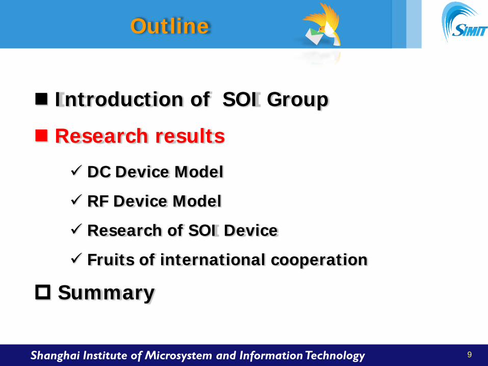
Outline
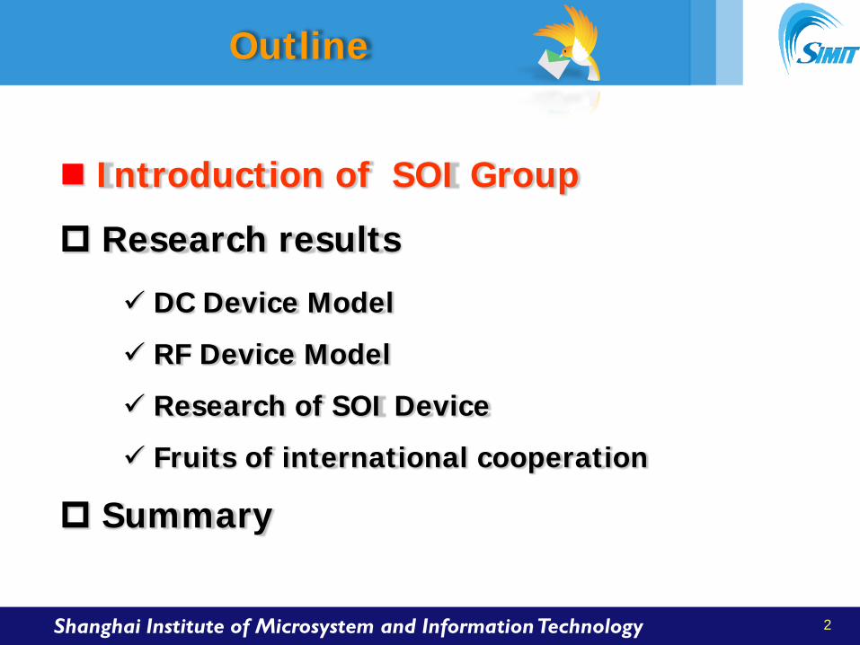
Introduction of SOI Group
Research results
Summary
DC Device Model
RF Device Model
Research of SOI Device
Fruits of international cooperation
2
Shanghai Institute of Microsystem and Information Technology
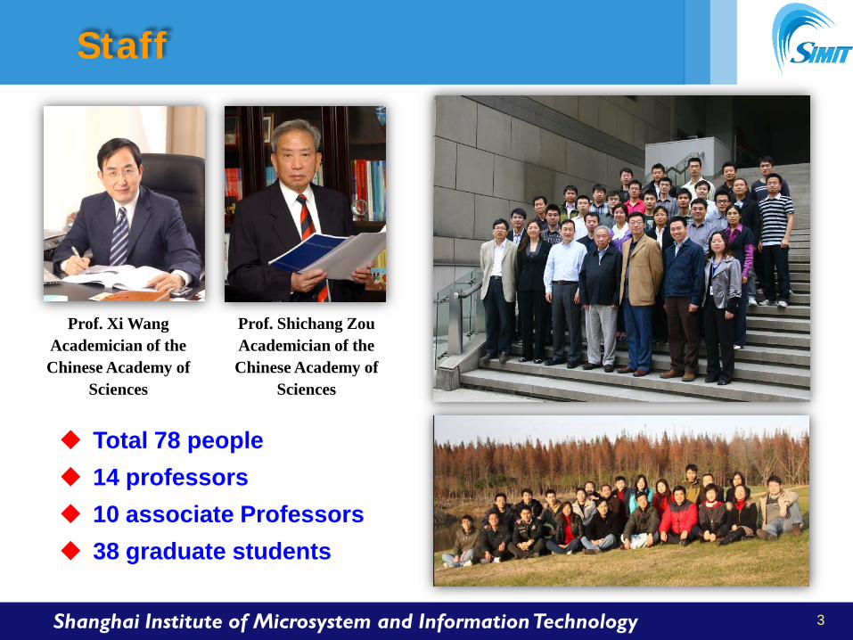
Staff
3
Prof. Xi Wang Academician of the Chinese Academy of
Sciences
Prof. Shichang ZouAcademician of the Chinese Academy of
Sciences
Total 78 people 14 professors 10 associate Professors 38 graduate students
Shanghai Institute of Microsystem and Information Technology 4
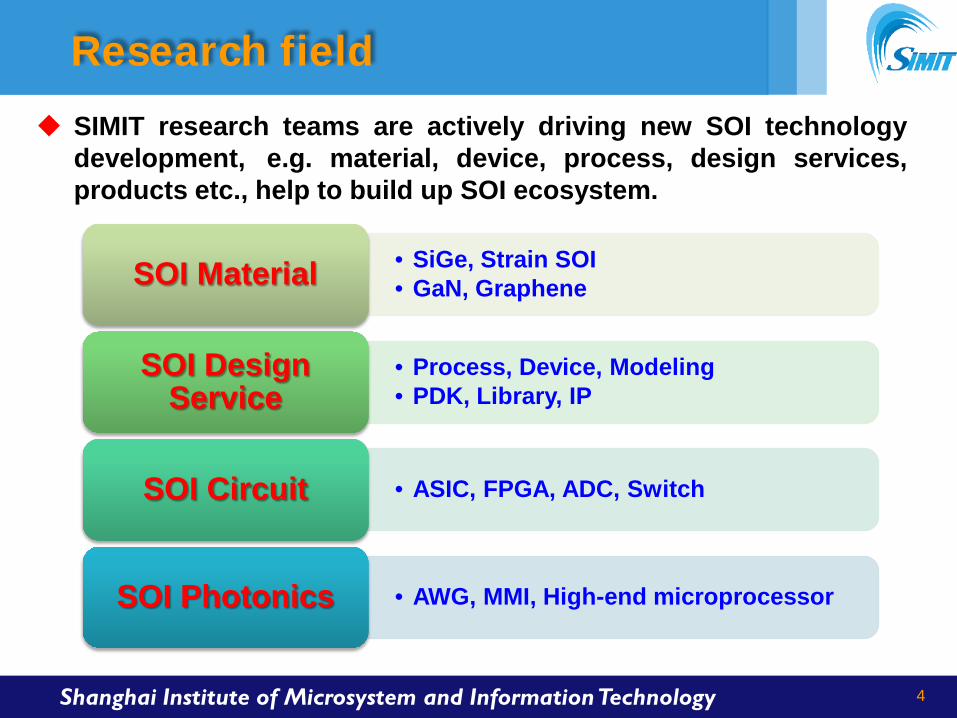
Research field
• SiGe, Strain SOI• GaN, GrapheneSOI Material
• Process, Device, Modeling• PDK, Library, IP
SOI Design Service
• ASIC, FPGA, ADC, SwitchSOI Circuit
• AWG, MMI, High-end microprocessorSOI Photonics
SIMIT research teams are actively driving new SOI technologydevelopment, e.g. material, device, process, design services,products etc., help to build up SOI ecosystem.

Shanghai Institute of Microsystem and Information Technology 5
100+ papers published, 150+ patents applied ( including 50+ international), within the last 5 years.
the Prize of National Science & Technology Advancement (1st grade)
Achievements

Shanghai Institute of Microsystem and Information Technology 6
SOI Roadmap in SIMIT
Simox Smart cut
0.13um SOI Logic Process0.2um SOI RF Process
Technology
PD SOI Technology FD SOI Technology
Substrates
1980s 2000s 2014s

Shanghai Institute of Microsystem and Information Technology 7
Model Laboratory - Hardware
Agilent B1500A Agilent B1542A Cascade EDGE Module Agilent N5244A PNA-X
Laboratory has the ability to test DC, RF and flick noise.
Electromagnetic shielding room Cascade Summit 12000 B-M

Shanghai Institute of Microsystem and Information Technology 8
Laboratory has a complete EDA solution for device modeling.
Sentaurus TCAD Tool
Cadence Tool
Agilent Model Tool
Model Laboratory - Software
Shanghai Institute of Microsystem and Information Technology
Outline
Introduction of SOI Group
Research results
Summary
9
DC Device Model
RF Device Model
Research of SOI Device
Fruits of international cooperation
Shanghai Institute of Microsystem and Information Technology 10
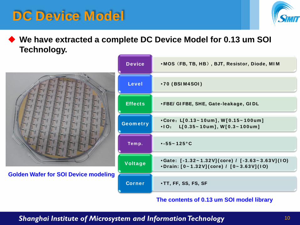
DC Device Model
•MOS(FB, TB, HB), BJT, Resistor, Diode, MIMDevice
•70 (BSIM4SOI)Level
•FBE/GIFBE, SHE, Gate-leakage, GIDLEffects
•Core:L[0.13~10um], W[0.15~100um]•IO: L[0.35~10um], W[0.3~100um]Geometry
•-55~125°CTemp.
•Gate: [-1.32~1.32V](core) / [-3.63~3.63V](IO)•Drain: [0~1.32V](core) / [0~3.63V](IO)Voltage
•TT, FF, SS, FS, SFCorner
We have extracted a complete DC Device Model for 0.13 um SOI Technology.
Golden Wafer for SOI Device modeling
The contents of 0.13 um SOI model library
Shanghai Institute of Microsystem and Information Technology 11
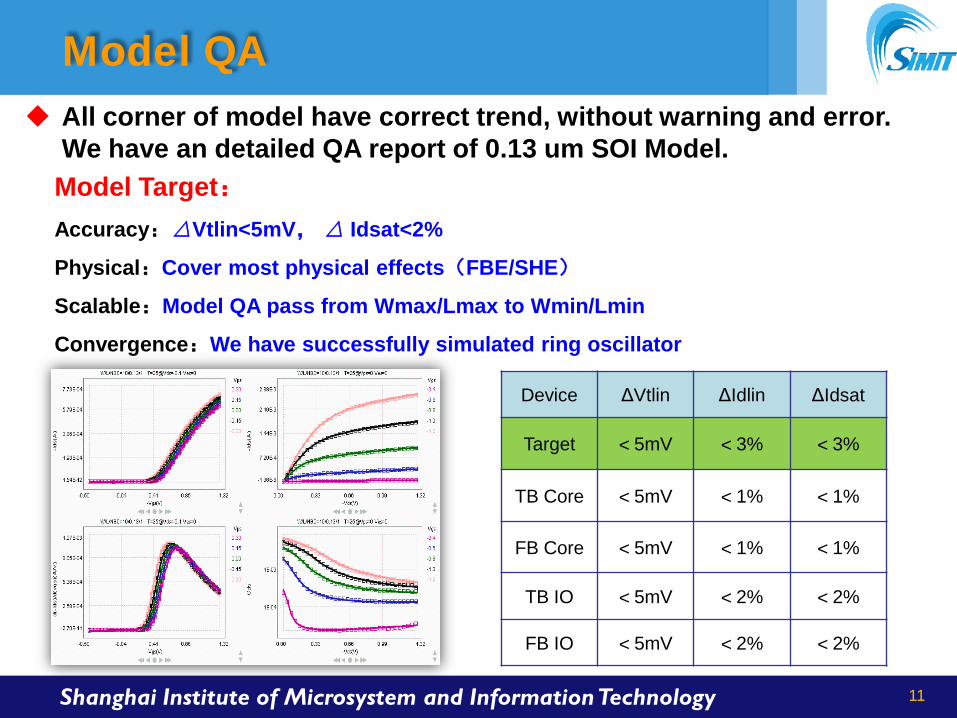
Model QA
Model Target:Accuracy:△Vtlin<5mV, △ Idsat<2%
Physical:Cover most physical effects(FBE/SHE)
Scalable:Model QA pass from Wmax/Lmax to Wmin/Lmin
Convergence:We have successfully simulated ring oscillator
Device ΔVtlin ΔIdlin ΔIdsat
Target <5mV <3% <3%
TB Core <5mV <1% <1%
FB Core <5mV <1% <1%
TB IO <5mV <2% <2%
FB IO <5mV <2% <2%
All corner of model have correct trend, without warning and error. We have an detailed QA report of 0.13 um SOI Model.

Shanghai Institute of Microsystem and Information Technology 12
Ring Oscillator Results
We have designed ring oscillator for the verification of SOI Model. As shown in the table, the simulation error is less than 10%.
Ring Oscillator Wp/Wn Lp/Ln FO FF SimulationDelay
TestDelay Accuracy
1.2V_FB_INV3/2 0.13/0.13 1 6 19.3 18.9 1.9%
2/1 0.13/0.13 1 6 21.7 21.8 -0.8%
3/2 0.13/0.13 3 5 40.4 38.7 4.5%
1.2V_TB_INV3/2 0.13/0.13 1 6 25.6 25.1 2.1%
2/1 0.13/0.13 1 6 29.2 29.7 -1.8%
3/2 0.13/0.13 3 5 52.8 50.2 5.3%
3.3V_FB_INV
3/2 0.30/0.35 1 6 41.1 39.9 3.1%
2/1 0.30/0.35 1 6 45.2 44 2.8%
3/2 0.30/0.35 3 5 88.8 86.3 2.8%
3.3V_TB_INV3/2 0.30/0.35 1 6 41.9 44 -4.6%2/1 0.30/0.35 1 6 47.3 49.8 -4.9%3/2 0.30/0.35 3 5 95.4 99.5 -4.1%
Shanghai Institute of Microsystem and Information Technology 13
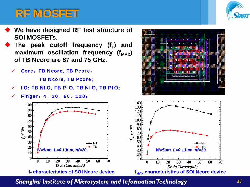
RF MOSFET We have designed RF test structure of
SOI MOSFETs. The peak cutoff frequency (fT) and
maximum oscillation frequency (fMAX)of TB Ncore are 87 and 75 GHz. Core:FB Ncore, FB Pcore,
TB Ncore, TB Pcore;
IO: FB NIO, FB PIO, TB NIO, TB PIO;
Finger:4,20,60,120;
0 10 20 30 40 50 60 700
102030405060708090
100
f t(GH
z)
Drain Current(mA)
FB TB
0 10 20 30 40 50 60 70102030405060708090
100110120130140
f max
(GH
z)
Drain Current(mA)
FB TB
fT characteristics of SOI Ncore device fMAX characteristics of SOI Ncore device
W=5um, L=0.13um, nf=20 W=5um, L=0.13um, nf=20

Shanghai Institute of Microsystem and Information Technology 14
Inductor
We have designedInductor test structure.
The peak of Q factor is16 in standard inductorwith N=5.5, W=9um,S=2um, D=255um.
freq [E+9]
L11
_mea
.m L
11_s
im [
E-9
]
0 5 10 15 20-20
-10
0
10
20
freq [E+9]
R11
_mea
R11
_sim
[E
+3]
0 5 10 15 200.0
0.5
1.0
1.5
2.0
freq [E+9] Q
11_m
ea Q
11_s
im [
E+
0]
0 5 10 15 20-10
-5
0
5
10
15
RF characteristics of 0.13 um SOI standard Inductor with N=5.5, W=9um, S=2um, D=255um.
Ring inductor Differential inductor

Shanghai Institute of Microsystem and Information Technology 15
RF Device Model
We have extracted RF Device Model for 0.13 um SOI Technology.
• MOS(TB, HB), Inductor, Resistor, • Varactor, MIM, MOMDevice
• 70 (BSIM4SOI)Level
• FBE/GIFBE, SHE, Gate-leakage, GIDLEffects
• Core: L[0.13~0.75um], W[1.5~8um]• IO: L[0.35~0.75um], W[1.5~8um]Geometry
• -55~125°CTemp.
•Gate: [-1.32~1.32V](core) / [-3.63~3.63V](IO)
•Drain: [0~1.32V](core) /[0~3.63V](IO)Voltage
• TT, FF, SS, FS, SFCornerSimulation result of RF NMOS
Shanghai Institute of Microsystem and Information Technology 16
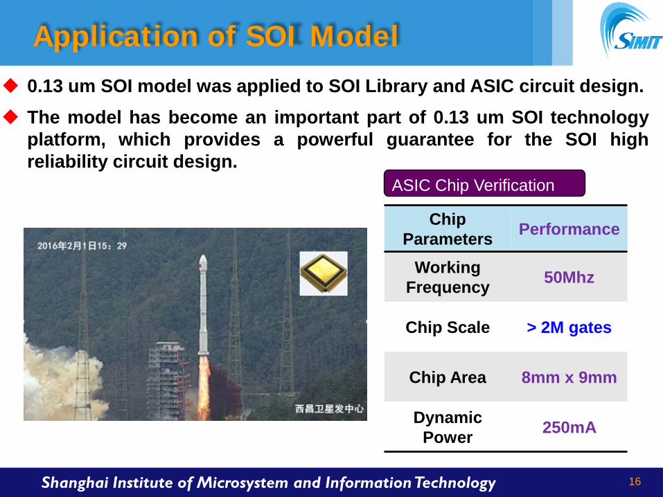
0.13 um SOI model was applied to SOI Library and ASIC circuit design. The model has become an important part of 0.13 um SOI technology
platform, which provides a powerful guarantee for the SOI highreliability circuit design.
Chip Parameters Performance
Working Frequency 50Mhz
Chip Scale > 2M gates
Chip Area 8mm x 9mm
Dynamic Power 250mA
ASIC Chip Verification
Application of SOI Model

Shanghai Institute of Microsystem and Information Technology 17
Novel Body Contact Structure
0.0 0.3 0.6 0.9 1.20
1
2
3
4
5
6
W/L=10um/0.13um
FB SOI TDBC SOI
PD SOI nMOSFET@VG=0.6~1.2V, Step=0.2V
Drai
n Cu
rrent
, I D(m
A)
Drain Voltage, VD (V)
•Jing Chen, Jiexin Luo et al., IEEE Electron Device Letters, 32(10), 1346, 2011•Jiexin Luo, Jing Chen et al., IEEE Transactions on Electron Devices, 59(1), 101, 2012•Kai Lu, Jing Chen et al., IEEE Electron Device Letters, 35(1), 15, 2014
-0.2 0.0 0.2 0.4 0.6 0.8 1.00
10
20
30
40
50
60
70
80
90
100
-0.2 0.0 0.2 0.4 0.6 0.8 1.0102030405060708090
100110120130140
f T(G
Hz)
VGS-VTH(V)
FB TB TDBC
(a) (b)
f MAX
(GH
z)
VGS-VTH(V)
FB TB TDBC
TDBC SOI devices without floating-body effects are successfullydemonstrated, which represent an improvement of 10% for the fTand of 90% for the fMAX compared with conventional T-gate body-contact devices.
Kink are perfectly suppressed in TDBC devices Superior RF performance of TDBC devices

Shanghai Institute of Microsystem and Information Technology 18
TDBC contact makes these SOI transistors strongly resistant to back channel radiation effects.
Jiexin Luo, Jing Chen et al., IEEE Transaction on Nuclear Science, 61(6), 11, 2014
-0.8 -0.4 0.0 0.4 0.8 1.210-13
10-11
10-9
10-7
10-5
10-3
increasing Total dose
pre 300krad(SiO2)
500krad(SiO2)
700krad(SiO2)
1Mrad(SiO2)
X-ray
TDBC SOI nMOSFETW=10µm, L=0.13µm
Drai
n Cu
rren
t, I D
(A)
Gate Voltage, VG(V)0 200 400 600 800 1000 120010-11
10-10
10-9
10-8
TDBC SOI@X-ray TB SOI@60Co γ-ray
∆ I O
FF (A
)Dose, rad (SiO2)
W/L=10µm/0.13µm
Total Dose Effects of TDBC SOI Ncore Total Dose Effects of TDBC and TB SOI
Total Dose Effects of TDBC Device
Cooperated with E. X. Zhang and D. M. Fleetwood, Vanderbilt University, USA

Shanghai Institute of Microsystem and Information Technology
Qingqing Wu, Jing Chen et al., IEEE Electron Device Letters, 33 (6), 743, 2012
We have experimentally demonstrated a novel capacitorless DRAMcell named FBGC on planar SOI CMOS technology .
FBGC has large noise margin and long retention time, also showsexcellent endurance nondestructive read characteristics and low-power operation.
Floating-Body/Gate Cell
Cooperated with Zhichao Lu and Jerry G. Fossum, University of Florida, USA
FBGC has large noise margin (26.5uA/um) and long retention time (560ms)
Schematic structure of FBGC
Shanghai Institute of Microsystem and Information Technology 20
0 1 2 3 4 5 6 7 8 9 10 11 12 13 14 15 16 17 18 19 20550
600
650
700
750
800
Brea
kdow
n (V)
the number of Device
50µm 60µm 70µm
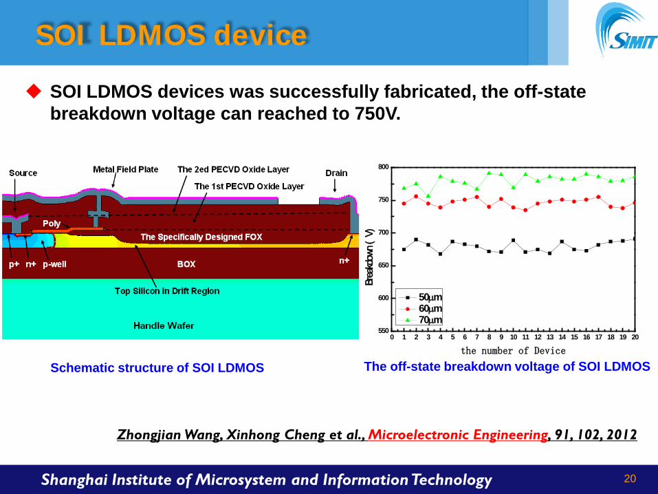
Zhongjian Wang, Xinhong Cheng et al., Microelectronic Engineering, 91, 102, 2012
SOI LDMOS device
SOI LDMOS devices was successfully fabricated, the off-state breakdown voltage can reached to 750V.
Schematic structure of SOI LDMOS The off-state breakdown voltage of SOI LDMOS

Shanghai Institute of Microsystem and Information Technology 21
Silicon Photonics
Physical Review Letters (2011.5.20), Editor’s Suggestion
移相单元
输入 输出
信号源 匹配电阻
in out
source resistor
phase shift cell
10Gbps transfer speedAPS special reported
It is expected to find applications in designing compact opticalcomponents to achieve the on-chip beam steering in photonic circuits.
Shanghai Institute of Microsystem and Information Technology 22
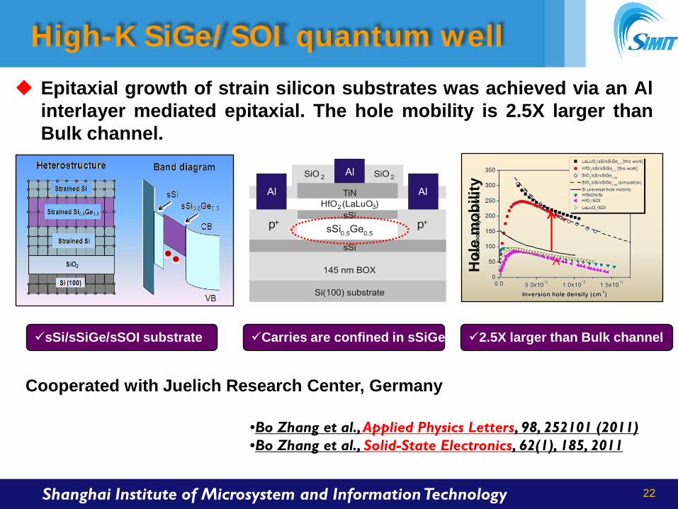
High-K SiGe/SOI quantum well
•Bo Zhang et al., Applied Physics Letters, 98, 252101 (2011)•Bo Zhang et al., Solid-State Electronics, 62(1), 185, 2011
sSi/sSiGe/sSOI substrate 2.5X larger than Bulk channelCarries are confined in sSiGe
Hol
e m
obili
ty
Cooperated with Juelich Research Center, Germany
Epitaxial growth of strain silicon substrates was achieved via an Alinterlayer mediated epitaxial. The hole mobility is 2.5X larger thanBulk channel.

Shanghai Institute of Microsystem and Information Technology 23
Nanowire on SOI
•Xin Ou et al., Nano Letters, 10(1), 171, 2010
Perfect structure with gate all-rounded
Easy to implement on SOI
Nanowire on Hybrid orientation SOI
100 nm
SSRM (Scanning Spreading Resistance Microscopy)
Cooperated with ForschungszentrumDresden-Rossendorf, Germany
•Xin Ou et al., Advanced Materials, 22(36), 4020, 2010
•Xiao Deyuan et al., Journal of Semiconductors, 30(1), 2009
SSRM has been used to characterize doping in silicon nanowire for the firsttime. The GAAC FinFET appears to be a good potential candidate forscaling down to sub-10 nm sizes.
Shanghai Institute of Microsystem and Information Technology
Outline
Introduction of SOI Group
Research results
Summary
24
DC Device Model
RF Device Model
Research of SOI Device
Fruits of international cooperation
Shanghai Institute of Microsystem and Information Technology 25
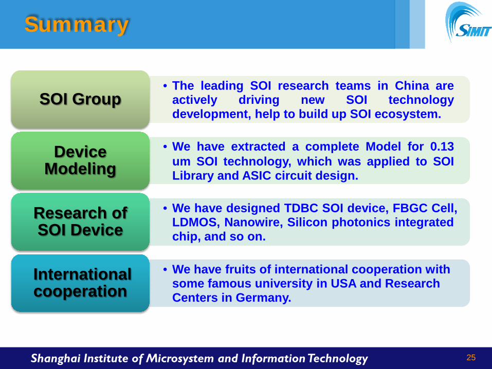
Summary
• The leading SOI research teams in China areactively driving new SOI technologydevelopment, help to build up SOI ecosystem.
SOI Group
• We have extracted a complete Model for 0.13um SOI technology, which was applied to SOILibrary and ASIC circuit design.
Device Modeling
• We have designed TDBC SOI device, FBGC Cell,LDMOS, Nanowire, Silicon photonics integratedchip, and so on.
Research of SOI Device
• We have fruits of international cooperation with some famous university in USA and Research Centers in Germany.
International cooperation

Shanghai Institute of Microsystem and Information Technology
Thank you !
26