research background of the project -...
TRANSCRIPT

i
4-bits 0.25 µm CMOS LOW POWER FLASH ADC
RAYED AWAD ABBAS AL-SAHLANEE
A thesis report submitted in partial
fulfilment of the requirement for the award of the
Degree of Master of Electrical Engineering
Faculty of Electrical and Electronic Engineering
Universiti Tun Hussein Onn Malaysia
January, 2015

v
ABSTRACT
The analogue to digital converters are the key components in modern electronic
systems. Signal processing is very important in many of the system on-a-chip
applications. Analogue to digital converters (ADCs) are a mixed signal device that
converts analogue signals which are real world signals to digital signals for
processing the information. As the digital signal processing industry grows the ADC
design with new techniques and methods are extensively sought after. This increases
the requirements on ADC design concerning for high speed, low power and small
area. A flash ADC is the best solution, not only for its fast data conversion rate but
also it becomes part of other types of ADC. However main problem with a flash
ADC is its power consumption, which increases in number of bits. In this project a 4-
bits flash ADC is designed with a 1.5V power supply and 1.5 GHz clock using 0.25
µm CMOS technology. The software used for this ADC design is Tanner EDA’s S-
EditTM
and T-SpiceTM
which is utilized to simulate the three blocks of flash ADC
with input frequency of 250 MHz. The ADC is successfully designed with a power
consumption of 5.18 mW.

vi
ABSTRAK
Penukar isyarat analog kepada digital adalah komponen utama dalam sistem
elektronik moden. Pemprosesan isyarat adalah sangat penting dalam pelbagai sistem
aplikasi menggunakan satu cip. Penukar isyarat analog kepada digital (ADC) adalah
peranti isyarat bercampur yang menukarkan isyarat analog iaitu isyarat dunia sebenar
kepada isyarat digital untuk memproses maklumat. Seiring dengan perkembangan
industri pemprosesan isyarat digital, reka bentuk ADC dengan teknik dan kaedah
baru secara meluas dicari dengan keperluan kepada rekabentuk ADC kelajuan yang
tinggi, penggunaan tenaga yang rendah dan bersaiz kecil. ADC denyar adalah
penyelesaian yang terbaik, bukan sahaja untuk kadar penukaran data yang cepat
tetapi juga ia menjadi sebahagian komponen kepada lain-lain jenis ADC. Namun
masalah utama dengan ADC denyar adalah penggunaan kuasa, yang meningkat
dengan bilangan bit. Dalam projek ini ADC denyar 4-bit direka dengan bekalan
kuasa 1.5V dan pemasaan 1.5 GHz menggunakan teknologi CMOS 0.25 μm.
Perisian yang digunakan untuk reka bentuk ADC ini ialah Tanner EDA S-EditTM
dan
T-SpiceTM
yang digunakan untuk mensimulasikan tiga blok ADC denyar dengan
menggunakan frekuensi input 250 MHz. Litar ADC ini telah berjaya direka dengan
penggunaan kuasa sebanyak 5.18 mW.

vii
CONTENT
TITLE i
DECLARATION ii
DEDICATION iii
ACKNOWLEDGEMENT iv
ABSTRACT v
ABSTRAK vi
CONTENTS vii
LIST OF TABLES ix
LIST OF FIGURES x
LIST OF SYMBOLS xii
LIST OF APPENDICES xiv
CHAPTER 1 INTRODUCTION
1.1 Project Background 1
1.2 Problem Statement 2
1.3 Project Objectives 2
1.4 Project Scopes 3
CHAPTER 2 LITERATURE REVIEW 2.1 Technology Development
4
4 2.2 ADC 5
2.3 Sampling Frequency 6
2.4 ADC Types 8
2.4.1 Flash ADC 8
2.4.2 Sigma-Delta ADC 10
2.4.3 Pipelined ADC 11
2.4.4 Successive Approximation ADC 12
2.4.5 Dual-Slope ADC 13
2.5 MOS Transistor Theory 14
2.6 Previous Research 17
2.6.1 Design and Implementation of a High Speed Low
Power 4-Bits Flash ADC 17
2.6.2 A 68 mW 1.356GS/s 4-Bit Flash ADC in 0.18μm
CMOS 18

viii
2.6.3 A 0.6 W 4 GS/s 4-Bit Flash ADC in 0.18 μm
CMOS 18
2.6.4 An Efficient Design of 3bit and 4bit Flash ADC 19
2.6.5 A 2.5 mW 1.25 GS/s 4-Bit Flash ADC in 90 nm
CMOS 19
CHAPTER 3 METHODOLOGY 20
3.1 Introduction 20
3.2 System Architecture 22
3.3 Flash ADC 22
3.3.1 Components of Flash ADC 24
3.3.1.1 Resistor Ladder 24
3.3.1.2 Comparator 25
(a) Resistive Driving Comparators 25
3.3.1.3 Encoder 27
(a) Multiplexer Encoders 27
3.4 Tanner EDA software
29
CHAPTER 4 RESULT AND ANALYSIS
30
4.1 Test and Simulations 30
4.2 The Resistor Ladder Circuit 31
4.2.1 The Resistor Ladder Circuit Simulation and
Results
33
4.3 Comparator Circuit 37
4.3.1 Comparator Circuit Simulation and Results 38
4.4 Encoder 40
4.4.1 Test and Simulation 2:1 Multiplexer 41
4.4.2 Test and Simulation 4 Bit Encoder 44
4.5 Test and Simulation All Stages of 4 Bit ADC 46
4.6 Final Results of 4 bit FLASH ADC 49
4.7 Power Consumption of 4 Bit Flash ADC 51
CHAPTER 5 CONCLUSION
53
5.1 Conclusion 53
5.2 Future Work 54
REFERENCES 55
APPENDICES 57

ix
LIST OF TABLES
TABLE NO. TITLE PAGE
2.1 Results for work [7] 17
4.1 The parameters for component used in the resistor ladder
circuit
33
4.2 The output of resistor ladder for 15 resistors 36
4.3 2:1 multiplexer truth table 40
4.4 2:1 multiplexer input values for testing 42
4.5 Multiplexer truth table for 4 bit encoder 44
4.6 4 bit encoder input values for testing 44
4.7 Input values for 4 bit ADC 47
4.8 Output voltages for 15 comparators 48
4.9 Thermometer bits output from 15 comparators 48
4.10 Comparison with previous work 52

x
LIST OF FIGURES
FIGURE NO. TITLE PAGE
2.1 Ideal Analog to Digital Converter 5
2.2 Sinusoids before and after digitization 6
2.3 Block diagram of flash ADC 9
2.4 Block diagram of sigma delta converter 10
2.5 Pipelined ADC with four 3-bit stages 11
2.6 Simplified N-bit SAR ADC architecture 12
2.7 Dual-slope integration 13
2.8 nMOS Transistor 15
2.9 pMOS Transistor 15
2.10 pMOS Transistor symbol 15
2.11 nMOS Transistor symbol 16
3.1 Flow chart for overall project activities 21
3.2 Block diagram of flash ADC 23
3.3 Resistor ladder 24
3.4 Resistive Divider Comparator 26
3.5 Architecture of multiplexer encoder 28
4.1 ADC 30
4.2 Resistor ladder 31
4.3 Resistor ladder full circuit 32
4.4 Output waveform of the resistor ladder circuit 33
4.5 Resistor voltage divider circuit for two resistors 34
4.6 Resistor voltage divider circuit for three resistors 35
4.7 Resistive divider comparator circuit and symbol 37
4.8 Comparator circuit used to test comparator 38
4.9 Output waveform of Comparator circuit with Vref =1.5 v 39
4.10 Output waveform of Comparator circuit with Vref =0.047 v 39
4.11 2:1 multiplexer with input and output 40

xi
4.12 2:1 multiplexer circuit 41
4.13 2:1 multiplexer circuit and symbol 41
4.14 2:1 multiplexer waveform output 42
4.15 11 2:1 multiplexer for 4 bit encoder 43
4.16 Output waveform for 4 encoder (0 0 1 1) 45
4.17 Output waveform for 4 encoder (0 1 1 0) 45
4.18 4 bit ADC Circuit 46
4.19 Waveforms for the 4 bit ADC comparator circuit 47
4.20 Output waveform of thermometer encoder 49
4.21 Output waveform of Vin = 0.75V at 250MHz 50
4.22 Output waveform of Vin = 1.15V at 250MHz 51

xii
List OF ABBREVIATIONS
VOUT Output voltage
VIN Input voltage
ID Drain current
W Width
L Length
VTH Threshold voltage
VGS Gate-to-source voltage
VSG Source-to-gate voltage
DC Direct current
IC Integrated circuit
CMOS Complementary M O S
MOS Metal oxide semiconductor
VLSI Very large scale integration
NGCC Nested gm-c
MOSFET Metal oxide field effect transistor
BJT Bipolar junction transistor
FET Field effect transistor
NMOS N-channel mosfet
PMOS P-channel mosfet
CS Common source
DRC Design rule check
CAD Computer added design
ADC Analogue-to-digital converter
DSP Digital signal processing
LSB Least significant bit
DAC Digital to analogue converter
CCD Charge-coupled device
SNR Signal to Noise Ratio
MSB Most significant bit
UWB Ultra-wideband
CMA Current-mode amplifiers

xiii
DS-CDMA Direct-spectrum code-division multiple-access
DSA Dual sense amplifiers
ENOB
Effective number of bits
INL Integrated Non-Linearity
DNL Differential Non-Linearity
DFF D flip-flop
MUX Multiplexer

xiv
LIST OF APPENDICES
TITLE PAGE
Appendix A Project’s T-Spice .sp code 58
Appendix B Result DC analysis output (.out) 63

CHAPTER 1
INTRODUCTION
1.1 Project Background
An analogue-to-digital converter (ADC) is a tool that translates the constant physical
amount of an analogue input into a digital number to denote the amplitude of that
amount, thus resulting in the translation of a series of digital values from a
continuous-time and continuous-amplitude analogue signal to a discrete-time and
discrete-amplitude digital signal [1]. A direct-conversion ADC or flash ADC consists
of a set of comparators [2] which test the input signal in parallel, with each firing
according to their decoded voltage range. An encoder logic circuit, which produces a
code for each voltage range, is fed by the set of comparators.
Among the various types of ADCs, the flash ADC is used as a component in
other types of ADCs such as pipeline and multi bit Sigma Delta ADCs. Among the
many principles employed for ADC circuits, the all-parallel or flash converter
remains the swiftest converter and it usually uses 2N-1 comparators for the
conversion of N bits data [3]. For large values of N, the greater number of
comparators are required and consequently the speed of the ADC will be slowed
down and the circuit will consume more power, this is main disadvantage of a flash
ADC that its power consumption is raised as the number of bits increased.
The design and execution of a high speed low power 4-bits 1.5 V, 0.25 µm
flash ADC using complementary metal oxide semiconductor (CMOS) technology is
presented in this study. The effect on the power consumption by altering the design
of the encoder block is being examined. The low power consumption is attributed to
the reduced size of the transistor and the modularity of the design.

2
1.2 Problem Statement
With the development of very large scale integration (VLSI) technology, the need for
lower power consumption, and higher speed and resolution in the ADC field has
become increasingly important. Currently, a lot of research is being carried out to
develop data converters that can meet the highest specifications for state-of-the-art
data converter applications. Novel methods have been put forward to reduce the
power consumption of flash ADCs. The flash ADC is not only renowned for its fast
data conversion rate, but is also a component of other types of ADCs such as pipeline
and multi bit Sigma Delta ADCs. However, main disadvantage of a flash ADC is its
power consumption, which goes up with an increase in the number of bits. Cascading
high-speed comparators are used to make flash ADCs. The circuit needs to use
2N -1 comparators for a converter with N bits. Many comparators are required for a
large value of N, and the consequent difficulty of encoding renders this principle less
appealing. This problem is discussed in this study, together with ways to overcome
it as well as the method for increasing the conversion rate.
1.3 Project Objectives
The main objective of this study is the design and execution of a high speed low
power 4-bits 1.5 V, 0.25 µm flash ADC employing CMOS technology. The
following are the objectives of this study:
a) To design a flash ADC using CMOS technology.
b) To obtain a power consumption of the ADC that is below 104 mW.

3
1.4 Project Scope
The main focus of this study is the flash ADC, and it consists of the design and
execution of the resistor ladder, comparator and encoder block of the flash ADC, and
the optimization of all the blocks to obtain a design that has a low power
consumption and high data conversion rate. It is also necessary to alter the
architecture of the encoder block and to monitor the effect of this on power
consumption. The scopes of this study are as follows:
a) The design of a encoder architecture for a 4-bits ADC.
b) The design of a circuit using a power supply of 1.5 V.
c) The use of CMOS technology of 0.25 µm.

CHAPTER 2
LITERATURE REVIEW
2.1 Technological Developments
Analogue-to-digital converters (ADC) constitute the main element in state-of-the-art
electronic systems. With the advancement of the digital signal processing industry,
researchers are faced with the increasing challenge of designing an innovative ADC.
Nowadays, the ADC is included in the chip of an electronic system and is no longer a
separate circuit for data converters, thus raising the ADC design requirements with
regard to such characteristics as high speed, low power, less area, high resolution,
low noise, etc. New methods and approaches are being constantly developed in order
to enhance the performance of ADCs. Among the various types of ADCs, the flash
ADC is the best, not only renowned for its data conversion rate, but also as a
component in other ADCs, such as the pipeline and multi bit Sigma Delta ADCs.
Analogue-to-digital converters are the foundational blocks that form an
interface between the analogue and digital domains. Since the ADC is the primary
block in mixed signal applications, it slows down data processing applications and
restricts the performance of the system. This chapter presents the architectures of
several A/D converters beginning with the basic definition of an ADC, followed by
descriptions of various ADC architectures, including Flash, Sigma-Delta, Pipeline,
Successive Approximation and Dual Slope ADCs.

5
2.2 ADC
An ADC is a mechanism that receives an analogue value (voltage/current) and
transforms it into digital form, thus enabling it to be processed by a microprocessor.
A simple ADC having two inputs and 8 output bits is shown in Figure 2.1. The input
comprises the signal that is to be transformed into digital form, while the reference
denotes the reference voltage (Vref) that is applied. The input signal in digital form is
indicated by the 8 bits at the output.
Figure 2.1: Ideal Analogue-to-Digital Converter
Input
Reference
Voltage
Output Bits (8)
10
8
6
4
2
32 64 96 128 160 192 224 255
Output Value (Decimal)
Referen
ce Volta
ge (V
ref)

6
2.3 Sampling Frequency
In signal processing, sampling is the reduction of a continuous signal to a discrete
signal. A common example is the conversion of a sound wave (a continuous signal)
to a sequence of samples (a discrete-time signal). Thus in ADC, proper sampling is
very important.
For a proper sampling, the analogue signal from the samples must be
accurately reconstructed. Even though the sampled data may seem to be unclear or
incomplete, if the process can be reversed, then it means that the key information has
been secured.
Figure 2.2 Sinusoids before and after digitization [4]
Figure 2.2 depicts several sinusoids before and after digitization. The
continuous line denotes the entry of the analogue signal into the ADC, while the
square markers represent the departure of the digital signal from the ADC. In Figure
2.2 (a), the analogue signal, which is a zero frequency cosine wave, has a constant
DC value. As the analogue signal comprises a sequence of straight lines between
each of the samples, all the information required to reconstruct the analogue signal is
enclosed in the digital data. This is defined as proper sampling.

7
In Figure 2.2 (b), the sine wave is shown to have a frequency of 0.09 of the
sampling rate. This might denote, for instance, the sampling of a 90 cycle/second
sine wave at 1000 samples/second. In other words, 11.1 samples are being taken at
the completion of each cycle of the sinusoid. This case is more complex than the
previous one because the analogue signal cannot be reconstructed by just drawing
straight lines between the data points. These samples must properly represent the
analogue signal, which they do, because no other sinusoid or sinusoid combination
will produce this pattern of samples. Since these samples match a single analogue
signal, therefore it means that the analogue signal can be accurately reconstructed.
This is another example of proper sampling.
The situation in Figure 2.2 (c) is much more difficult as the frequency of the
sine wave has been increased to 0.31 of the sampling rate, thus resulting in only 3.2
samples per sine wave cycle. The samples here are so scanty that they not even seem
to follow the general pattern of the analogue signal. These samples must properly
represent the analogue waveform, which again they do, and for precisely the same
reason. The samples distinctly represent the analogue signal. All the information that
is required to reconstruct the continuous waveform is maintained in the digital data.
Clearly, it must involve a more sophisticated technique than merely drawing straight
lines between the data points. Although this may appear to be strange, this falls under
the definition of proper sampling.
In Figure 2.2 (d), the analogue frequency is forced even higher to 0.95 of the
sampling rate, with a meagre 1.05 samples per sine wave cycle. In this case, the
samples fail to properly represent the data. Instead, they depict a different sine wave
from the one enclosed in the analogue signal. Specifically, the initial 0.95 frequency
sine wave is misrepresented as a 0.05 frequency sine wave in the digital signal. This
occurrence of sinusoids changing frequency during sampling is known as aliasing.
The sinusoid adopts another frequency that is not its own in much the same way as a
criminal might adopt an assumed name or identity (an alias). An unambiguous
reconstruction is no longer possible as the digital data cease to be uniquely connected
to a specific analogue signal. Nothing in the sampled data indicates that the initial
analogue signal had a frequency of 0.95 instead of 0.05. The sine wave has totally
concealed its true identity; thus committing the perfect crime.
This is defined as improper sampling. This line of reasoning is a
breakthrough in the digital signal processing (DSP) sampling theorem, which is

8
often called the Shannon or the Nyquist sampling theorem, after the authors who
published papers on this subject in the 1940s. According to this theorem, a constant
signal can only be properly sampled if it is not comprised of frequency components
that are more than half the sampling rate. For example, a sampling rate of 2,000
samples/second will need an analogue signal that is comprised of frequencies that are
less than 1000 cycles/second. If the signal has frequencies that are beyond this limit,
those frequencies will have aliases of between 0 and 1000 cycles/second combining
with any information that was rightfully there.
2.4 ADC Types
2.4.1 Flash ADC
Flash ADC’s are also known as parallel ADCs because of their parallel design,
which makes them the fastest type of ADCs that are appropriate for use with high
bandwidths. Conversely, the flash ADC has high power consumption, low resolution,
and is costly for high resolution applications. It is employed primarily in high
frequency applications and in the other types of ADC designs, such as Pipelined and
the multi-bit Sigma-Delta ADC. Some examples of flash ADC applications include
data acquisition, satellite communication, radar processing, sampling oscilloscopes,
and high-density disk drives. From Figure 2.3, which is a block diagram of a
standard flash ADC, it can be seen that an “N” bit converter would need to have 2N-1
comparators.

9
Figure 2.3. Block Diagram of Flash ADC
The comparators will generate a thermometer code of an input signal. It is called
thermometer code encoding, because it is similar to a mercury thermometer, where
the mercury column always rises to the appropriate temperature and no mercury is
present above that temperature. This thermometer code will then encode into a binary
form by thermometer-to-binary encoder. The comparators are typically a cascade of
wideband and low gain stages. They are low gain because at high frequencies it is
difficult to obtain both wide bandwidth and high gain. They are designed for low
voltage offset, such that the input offset of each comparator is smaller than a Least
significant bit (LSB) of the ADC. Otherwise, the comparator's offset could falsely
trip the comparator, resulting in a digital output code not representative of a
thermometer code. A regenerative latch at each comparator output stores the result.
The latch has positive feedback, so that the end state is forced to either a "1" or a
"0"”

10
2.4.2 Sigma-Delta ADC
Figure 2.4 shows a sigma-delta ADC that uses a 1-bit DAC, filtering, and over
sampling to achieve very accurate conversions.
Figure 2.4: Block Diagram of Sigma Delta Converter [5]
When a low frequency input signal is applied to a Sigma-Delta ADC, this
signal will be quantized with a high sampling frequency by the 1-Bit digital to
analogue converter (DAC). The sampling rate will be lowered and the ADC
resolution will be raised by the digital decimator filter. For example, given a
sampling frequency of 2MHz, then the sampling rate will be lowered to
approximately 8 kHz, and the ADC resolution or dynamic range will be raised to 16
bits due to the oversampling.
The Sigma-Delta ADC is renowned for its accuracy with regard to the input
reference and clock rate, and it is unlike the flash ADC, where the accuracy of the
conversion is affected by the resistors. Another advantage of the Sigma-Delta
converter is that it is inexpensive.
However, the Sigma-Delta converter is hampered by its speed, as it is known
to be the slowest type of ADC converter. The converter requires many clock cycles
to carry out oversampling of the input for conversion. Another disadvantage of the
Sigma-Delta converter is the complex design of the digital filter, which is used to
transform duty cycle information into digital words.

11
2.4.3 Pipelined ADC
One of the most common ADC designs is the pipelined analogue-to-digital
converter, which can operate on a few mega samples to more than hundreds of mega
samples with a resolution ranging from 8 bits to 16 bits. It is used extensively in the
medical and communications field, such as for charge-coupled device (CCD)
imaging, ultrasonic medical imaging, digital receivers, base stations, digital videos
(for example, HDTV), xDSL, modem cables, and fast Ethernet, because of its high
resolution and sampling rate range. Although there are vast improvements in terms of
speed, resolution, power and dynamic performance in the pipelined ADC, the SAR
and integrating designs are still being employed for low sampling rate applications,
whereas the flash ADC is still preferred for high sampling rate applications (e.g. 1
GHz). Figure 2.5 shows the block diagram of a 12-bit pipelined ADC.
Figure 2.5 Pipelined ADC with four 3-bit stages [6]

12
2.4.4 Successive Approximation ADC
Successive-approximation-register (SAR) analogue-to-digital converters (ADCs) are
used mainly for medium to high-resolution and low sampling rate applications, the
majority of which are in the range of 8 bits to 16 bits. It also consumes very little
power and has a small form factor. As such, it is ideal for low power applications, for
example, for portable/battery-powered instruments, pen digitizers, industrial controls,
and data/signal acquisitions. In fact, since the SAR ADC executes a binary search
algorithm, therefore its internal circuitry might operate at several megahertz.
However, because of the approximation algorithm that follows, the sampling rate of
the ADC is quite low. Figure 2.6 shows the basic configuration of the SAR ADC,
although it can be implemented in several different ways.
Figure 2.6: Simplified N-bit SAR ADC architecture [6]
13
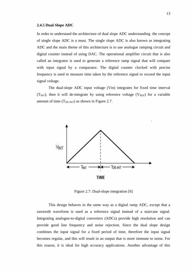
2.4.5 Dual-Slope ADC
In order to understand the architecture of dual slope ADC understanding the concept
of single slope ADC is a must. The single slope ADC is also known as integrating
ADC and the main theme of this architecture is to use analogue ramping circuit and
digital counter instead of using DAC. The operational amplifier circuit that is also
called an integrator is used to generate a reference ramp signal that will compare
with input signal by a comparator. The digital counter clocked with precise
frequency is used to measure time taken by the reference signal to exceed the input
signal voltage.
The dual-slope ADC input voltage (Vin) integrates for fixed time interval
(TINT), then it will de-integrate by using reference voltage (VREF) for a variable
amount of time (TDE-INT) as shown in Figure 2.7.
Figure 2.7: Dual-slope integration [6]
This design behaves in the same way as a digital ramp ADC, except that a
sawtooth waveform is used as a reference signal instead of a staircase signal.
Integrating analogue-to-digital converters (ADCs) provide high resolution and can
provide good line frequency and noise rejection. Since the dual slope design
combines the input signal for a fixed period of time, therefore the input signal
becomes regular, and this will result in an output that is more immune to noise. For
this reason, it is ideal for high accuracy applications. Another advantage of this

14
design is that it is less complicated since it does not include a DAC. A major
constraint of this design is that it is only appropriate for input signals at low
bandwidths.
2.5 The MOS Transistor Theory
A bipolar junction transistor is able to intensify a small alteration in the input current
to generate a large alteration in the output current. Another type of transistor, known
as a field effect transistor (FET), can transform an alteration in input voltage into an
alteration in the output current. Hence, the performance of an FET is measured in
terms of its transconductance, which is the ratio of the alteration in the output current
to the alteration in the input voltage. The voltage is directed at the input terminal,
known as the Gate, and the current that flows through the transistor is determined by
the electric field generated by the gate voltage. An insulating plate is located beneath
the gate electrode, and hence, the gate current of an FET is roughly zero. Metal
Oxide Semiconductor (MOS) transistors or Metal Oxide Semiconductor Field Effect
Transistors (MOSFET) are FETs which employ a slim silicon dioxide insulator.
MOS transistors are categorised as N-channel transistors (nMOS) and P-
channel transistors (pMOS) according to the channel formed below the insulating
layer. Figure 2.8 and 2.9 show the cross sections of both transistors and Figure 2.10
and 2.11 show the symbol of the transistor. Each transistor is comprised of a source,
drain, gate and a backgate, commonly called the bulk terminal. The source and gate
are produced by the dispersion of the N-type dopant to a P substrate for NMOS,
while the reverse is true for PMOS. The MOS transistor has a source and drain that
are interchangeable, whereby the carriers flow out from the source and into the drain.

15
Figure 2.8: nMOS transistor
Figure 2.9: pMOS transistor
Figure 2.10: pMOS transistor symbol

16
Figure 2.11: nMOS transistor symbol
A description of the basic operation of an NMOS transistor is given below. A
transistor has three operational regions:
1. Cut-off region (VGS < VTH)
2. Triode region (VGS > VTH & VDS < VDSsat)
3. Saturation region (VGS > VTH & VDS > VDSsat)
At first, the transistor is regarded as having VGS = 0, i.e. there is no gate to the
source voltage that is applied. It is similar to having the backs of 2 diodes connected
to each other between the source and the drain, such that no current will flow from
the source to the drain. In addition, a depletion region will be created at the source –
substrate, drain – substrate junctions. When the VGS voltage is steadily increased to
below the threshold voltage (VTH), the holes beneath the gate are held off to generate
a depletion region, and it becomes steady beneath the gate from the source to the
drain. When the VGS is then increased beyond the threshold voltage, i.e.
VGS > VTH, the minority carriers (electrons) in the P sub crosses the depletion region
and arrives beneath the gate. This process is known as inversion. The number of
electrons that arrives beneath the gate is determined by the VGS – VTH voltage.
Therefore, a conducting channel is generated as a result of this transverse electric
field. After the channel is formed between the Source and the Drain, the VDS (Drain
to source voltage) is steadily increased from 0. When the VDS changes to positive, the
Drain – Sub junction will become reverse biased, and the depletion region will
become wider as the drain becomes increasingly positive with regard to the source.
Because of this adjacent electric field, the current flow begins from the source to the

17
drain, and this flow will increase as the VDS increases. Hence, the potential at the
source is below that of the source at the depletion region, which widens close to the
drain while the channel narrows. The channel comes into contact with the drain the
moment the VDS = VDSsat, and the resultant drain to source voltage is then called the
pinch-off voltage. The current flow becomes steady beyond the saturation voltage.
Carriers are driven down the channel by the somewhat weak electric field along the
channel. On arriving at the edge of the pinched-off region, they are swept across the
depletion region by the strong electric field. As the drain voltage increases, there is
no further drop in the voltage across the channel but instead, the pinched-off region
broadens. Thus, the drain current reaches the threshold and stops rising.
2.6 Previous Research
2.6.1 Design and Implementation of a High Speed Low Power 4-Bits Flash ADC
A four-bit flash type Analog-to-Digital Converter (ADC) is designed and it is
suitable for Ultra Wide Band (UWB) applications due to its high operating frequency
and low power consumption. The high operating frequency is due to the pipelined
nature of the design. The low power consumption is due to the minimized transistor
sizes and modularity of the design. The proposed ADC is designed, integrated and
simulated using Cadence EDA Tools. The simulation was done using a 3.3V, 0.35μm
CMOS Technology [7]. Table 2.1 summarizes the result of this project.
Table 2.1 Results for work [7].
Parameters [7]
Power supply 3.3 (V)
Input frequency 250 (MHz)
CLK frequency 1.3 (GHz)
Stages 5
Power consumption 104 (mW)

18
2.6.2 A 68 mW 1.356 GS/s 4-Bit Flash ADC in 0.18 μm CMOS
A 1.356 GS/s 4-bit ADC meant for direct-spectrum code-division multiple-access
ultra-wideband (DS-CDMA UWB) communications was introduced in [8]. A flash
architecture that is totally differential was employed by the ADC. In order to keep
the power consumption low and to attain a high rate of conversion, the recommended
converter was designed with a preamplifier range comprised of current-mode
amplifiers (CMAs), accompanied by dual sense amplifiers (DSAs). The dual sense
amplifier is able to detect both the voltage and the contrasts in the currents of the
preamplifier output signals. At an input of 30 MHz (650 MHz), the ADC was able to
attain an effective number of bits (ENOB) of 3.7 (3.35) while experimenting at 1.356
GHz. A current of 38 mA was drawn from a power supply of 1.8V. The ADC, with
an active area of 0.35 mm2, was assembled through a 0.18 μm CMOS process.
2.6.3 A 0.6 W 4GS/s 4-Bit Flash ADC in 0.18 μm CMOS
A 4-bit flash ADC executed in 0.18 μm digital CMOS to achieve a sampling rate of 4
GS/s was presented in [9] and [10]. The ADC’s comparator comprised of a
comparator core, two latch stages and a subsequent D flip-flop (DFF). A high
comparator speed was achieved by means of on-chip differential inductors (32 μm by
32 μm) within the comparator core, and small rapid mechanisms. In order to lessen
the Integrated Non-Linearity (INL) and Differential Non-Linearity (DNL) errors, the
DAC trimming was used in combination with the comparator redundancy. An ENOB
of 3.84 and 3.48 bits was achieved for a 100 MHz input tested at 3 and 4 GS/s,
respectively. A Wallace tree counter [11] was employed for the conversion from a
thermometer code to a binary code, as well as for enhanced resistance to
metastability and bubble errors. To ensure that the counter functioned properly at 4
GS/s, two time-interleaved counters operating at 50% of the comparator clock
frequency (i.e., 2GHz) were used in the ADC. The power consumption of the ADC
together with the clock buffer was approximately 0.6 W from a power supply of 1.8
V (for the analogue part) and from 2.1 V to 2.5 V (for the digital part), while the
input capacitance was 1.6 pF.

19
2.6.4 Efficient Design of a 3-bit and 4-bit Flash ADC
The efficiency of a flash Analogue-to-Digital converter depends very much on the
type of comparator and the design of the thermometer-to-binary encoder used. A
description of the design and pre-simulation of a 3-bit and 4-bit ADC for low power
CMOS is presented in this paper. In order to convert a thermometer code to a binary
code it is necessary to have 2N-1 comparators and an encoder. A spectre simulator
using 90 nm technology was employed to simulate the design in a Cadence
environment. Prior to the simulation, the design displayed a low power dissipation of
87 uw for the comparator, and 1.05 mW and 1.984 mW for the 3-bit and 4-bit Flash
ADC, respectively. Meanwhile, the circuit functioned at an input frequency of 25
MHz for a power supply of 1.5 V, with a conversion time of 2.162 ns and 6.182 ns
for the 3-bit and 4-bit ADC, respectively [12].
2.6.5 A 2.5mW 1.25GS/s 4-Bit Flash ADC in 90nm CMOS
A very low power 1.25GS/s 4-bit flash ADC in 90 nm CMOS was described in [13].
It is able to attain 3.7 effective number of bits (ENOB) from a DC to a Nyquist rate
input with a power consumption of 2.5 mW from a 1.2 V supply, thus resulting in an
energy per conversion rate of 0.16 pJ. Every inessential block in the flash ADC was
detached, including the track/hold (T/H), preamplifiers, reference ladder, and bubble
error correction, in order to conserve power. Threshold levels were built into the
comparators by means of appropriate sizing of the input transistor pairs and active
calibration by a binary scaled range of variable capacitors. The outputs from the
comparators were accumulated in Set-Reset latches and then transformed into a 4-bit
Gray code (with inherent error correcting features) by means of a ROM-based
encoder. NAND gates with 2 inputs were used to conduct the word-line selection of
the encoder.
CHAPTER 3
METHODOLOGY
3.1 Introduction
When designing a conversion system, it is necessary to understand the operation of
the complete electronic system in which it is to be installed before determining the
design specifications of the converter. A flowchart of the steps leading to the design
or selection of a typical conversion system is shown in Figure 3.1. If the system
designer were to merely concentrate on the design of the conversion system without
regard for the operating system, then problems are bound to arise during the
development of the equipment. On the other hand, by taking into account all the
problems of the system, the designer will be able to save time and costs when it
comes to develop the equipment.
This study employs the methods as mentioned to develop and implement a
high speed, low power, 4-bit Flash ADC using 1.5 V and 0.25 µm CMOS technology
to reduce power consumption, reduce area and increase the speed. The study is
divided into several parts.
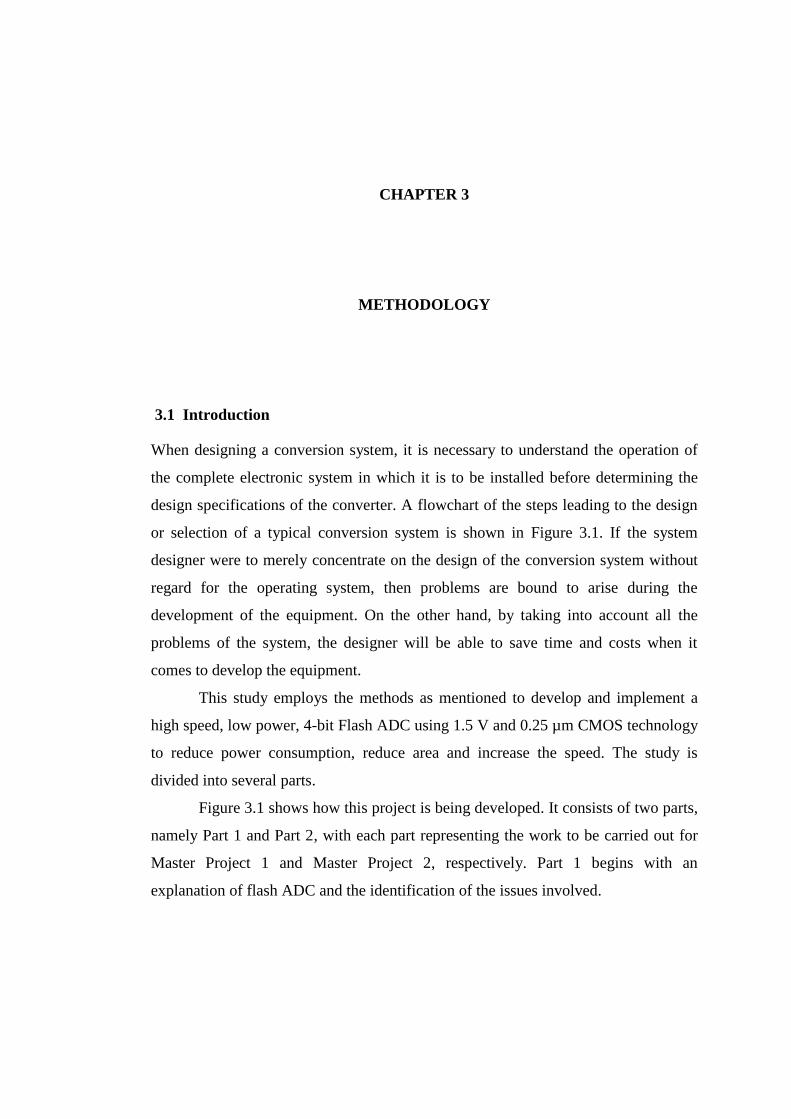
Figure 3.1 shows how this project is being developed. It consists of two parts,
namely Part 1 and Part 2, with each part representing the work to be carried out for
Master Project 1 and Master Project 2, respectively. Part 1 begins with an
explanation of flash ADC and the identification of the issues involved.

21
Figure 3.1: Flow chart of overall project activities
No
No
Yes
Performance Evaluation of the Integrated Circuit
PART 1
PART 2
Testing & Achieve
Output
Specification Design Requirement
Design and Test the Comparators
Design and Test the encoder
Yes
Testing & Achieve
Output
Problem Statement
Literature Review
Start
End

22
3.2 System Architecture
Several architectures are available for the development of an ADC based on the
speed, accuracy, resolution, and so on, with the most popular ADC types being the
flash, pipeline, successive approximation, dual slope and sigma-delta. Flash ADC
has been chosen for this project and will be discussed further.
3.3 Flash ADC
The flash ADC, also known as a parallel ADC, is the fastest among all the other
ADCs because of its parallel architecture, making it suitable for high bandwidth
applications. However, it uses up a lot of energy for low resolutions, and is costly for
high resolutions. It is used primarily in high frequency applications and in the other
ADC architectures such as the pipeline and multi-bit sigma delta ADCs. Some
applications of flash ADCs include data acquisition, satellite communication, radar
processing, sampling oscilloscopes, and high-density disk drives.
From the block diagram of a typical flash ADC as shown in Figure 3.2, it can
be seen that 2N-1 comparators are needed for an N bit converter. The resistor ladder
network is made up of 2N resistors, which produce reference voltages for the
comparators. Each comparator has a reference voltage that is one least significant bit
(LSB) less than that of the comparator directly above it. The comparator will
generate a “1” when its analogue input voltage exceeds its reference voltage; if not,
the comparator output is "0". If the analogue input lies between Vx4 and Vx5, then
the comparators X1 up to X4 will generate "1"s, while all the remaining comparators
will generate "0"s. The point where the code changes from ones to zeros is the point
at which the input signal becomes smaller than the respective comparator reference-
voltage levels.
For this project, since the ADC is for 4-bits, then the number of comparators
are 24-1= 15. As for the resistor, the numbers are 2
4 = 16.

23
Figure 3.2: Block Diagram of Flash ADC [11]
Resistor ladder circuit
Comparator
input

24
3.3.1 Components of Flash ADC
A range of comparators are used in a flash ADC to compare the input voltage with a
series of increasing reference voltages. The input signal is denoted by the comparator
output as a thermometer code [12], which will then be converted into a binary code.
This explanation clearly shows that practically all flash ADCs consist of three blocks
as follows:
1. Resistor Ladder
2. Comparator
3. Encoder
3.3.1.1 Resistor Ladder
A resistor ladder is used to produce the reference voltages for the comparators in a
flash Analogue-to-Digital Converter. In a continuous time system, the input signal
and the reference voltage are linked directly to the differential pairs of the amplifier.
The differential pairs of the input amplifier that are functioning in the linear range
have an input capacitance that connects the source of the input signal with the ladder,
thus resulting in a decline in the reference voltages. Since the position of the zero
crossing produced at the input gain stage is determined by the reference voltage, this
will distort the A/D converter. It is necessary to compute the maximum impedance of
the reference ladder in order to avoid significant reference ladder feed-through. A
distributed model for the computation of the maximum allowable reference ladder
resistance for a specific shift in the reference voltages is shown in Figure 3.3.
Figure 3.3: Resistor Ladder

55
REFERENCES
[1] R. van de Plassche, Integrated Analog-to-Digital and Digital-to-Analog
Converters, ADCs, Kluwer Academic Publishers, 1994.
[2] Malmstadt, Enke and Crouch, Electronics and Instrumentation for
Scientists, The Benjamin/Cummings Publishing Company, Inc., 1981.
[3] Tocci, Ronald J., Digital Systems, 5th Ed, Prentice-Hall, 1991.
[4] Steven W. Smith, The Scientist and Engineer's Guide to Digital Signal
Processing, 1997.
[5] R. Jacob Baker, CMOS Mixed-Signal Circuit Design 2nd Ed. Wiley-IEEE.
2009.
[6] S. Sumathi and P. Surekha, LabVIEW Based Advanced Instrumentation
Systems, 2007.
[7] Shehata, K.A., Design and Implementation of a High Speed Low Power 4-
bit Flash ADC, Design & Technology of Integrated Systems in Nanoscale
Era, IEEE, Rabat, pp. 200-203. 2-5 sept. 2007.
[8] J. H. Koo, Y. J. Kim, B. H. Park, S. S. Choi, S. I. Lim, and S. Kim, A
4-bit 1.356 GSps ADC for DS-CDMA UWB system, IEEE Asian Solid-
State Circuits Conference, pp. 339 -342, November 2006.
[9] S. Park, Y. Palaskas, and M. P. Flynn, A 4-GS/s 4-bit F l a s h ADC
in 0.18µm CMOS, IEEE Journal of Solid-State Circuits, vol. 42, pp.
1865-1872, September 2007.
[10] S. Park, Y. Palaskas, and M. P. Flynn, A 4GS/s 4b Flash ADC in 0.18µm
CMOS, IEEE International Solid-State Circuits Conference (ISSCC) Digest
of Technical Papers, pp. 570–571, February 2006.
[11] F. Kaess, R. Kanan, B. Hochet, and M. Declercq, New Encoding Scheme
for High-speed Flash ADCs, IEEE International Symposium on Circuits
and Systems (ISCAS), pp. 878–882, June 1997.
[12] Arunkumar P Chavan, An Efficient Design of 3bit and 4bit Flash ADC,

56
International Journal of Computer Applications (0975 – 8887) Volume 61–
No. 11, January 2013.
[13] G. Van der Plas, S. Decoutere, and S. Donnay, A 0.16pJ/ Conversion-
Step 2.5mW 1.25GS/s 4b ADC in a 90nm Digital CMOS Process, IEEE
International Solid-State Circuits Conference (ISSCC) Digest of Technical
Papers, pp. 2310-2311, February 2006.
[14] R. Jacob Baker, CMOS Circuit Design, Layout, and Simulation, 3rd Ed,
Wiley-IEEE Press, 2010.
[15] Khalid Sayood, Data Compression, 3rd Ed, Morgan Kaufmann. Professor
K.R Rao, EE5359 Principles of Digital Video Coding, 2005.
[16] Jincheol Yoo, Kyusun Choi and Tangel, A 1-GSPS CMOS Flash A/D
Converter for System-on-chip Applications, IEEE Computer Society
Workshop on 19-20 April 2001 pp 135–139. 2001.
[17] Harris, David, Digital Design and Computer Architecture. Penrose. p. 79.
2007.