research article cloud computing for rigorous coupled-wave analysis - hindawi
TRANSCRIPT

Hindawi Publishing CorporationAdvances in Optical TechnologiesVolume 2012, Article ID 398341, 7 pagesdoi:10.1155/2012/398341
Research Article
Cloud Computing for Rigorous Coupled-Wave Analysis
N. L. Kazanskiy1 and P. G. Serafimovich2
1 Image Processing Systems Institute, Russian Academy of Sciences, Samara 443001, Russia2 S.P. Korolyov Samara State Aerospace University, Samara 443086, Russia
Correspondence should be addressed to P. G. Serafimovich, [email protected]
Received 11 April 2012; Accepted 7 June 2012
Academic Editor: Augusto Belendez
Copyright © 2012 N. L. Kazanskiy and P. G. Serafimovich. This is an open access article distributed under the Creative CommonsAttribution License, which permits unrestricted use, distribution, and reproduction in any medium, provided the original work isproperly cited.
Design and analysis of complex nanophotonic and nanoelectronic structures require significant computing resources. Cloudcomputing infrastructure allows distributed parallel applications to achieve greater scalability and fault tolerance. The problemsof effective use of high-performance computing systems for modeling and simulation of subwavelength diffraction gratings areconsidered. Rigorous coupled-wave analysis (RCWA) is adapted to cloud computing environment. In order to accomplish this,data flow of the RCWA is analyzed and CPU-intensive operations are converted to data-intensive operations. The generated datasets are structured in accordance with the requirements of MapReduce technology.
1. Introduction
In recent years there has been a steady increase in the researchand development activity in the nanoscale fabrication area.Optical methods are widely used to characterize nanoelec-tronic and optimize nanophotonic structures [1–4]. Whenthe characteristic size of the nanostructure is comparableto the wavelength of the used light, the conventional scalardiffraction methods become inadequate. Therefore, rigorousMaxwell’s electromagnetic theory should be adopted toanalyze such structures. With the advances of computer tech-nology, many numerical techniques have been developed torigorously solve the diffraction problem.
Rigorous-coupled wave analysis (RCWA) [5–10] hasbeen frequently used to solve the problem of electromagneticwave diffraction by periodic structures. Solving optimiza-tion and scatterometry problems may require millions ofdiffraction pattern evaluations for each possible combinationof geometric structure and incident light parameters. Com-putational cost estimate shows that these problems wouldclearly call for supercomputing capacity.
Thus, current computational tasks of nanostructureanalysis generate ever-higher demands on the methods usedfor parallel computing and data storage [11, 12]. The devel-oped applications should work efficiently on multicore and
multiprocessor systems. An implementation of MPI (mes-sage passing interface) is the traditional means of creatingsuch applications [13]. MPI provides a highly flexible abilityto develop applications that address specific requirements ofthe algorithm structure and the used computing infrastruc-ture. However, this ability makes it necessary for developersto implement some of the low-level services.
Compared with MPI, MapReduce programming para-digm for cloud computing [14] provides higher level ofabstraction for the developer of parallel applications. On theone hand, MapReduce imposes certain restrictions on dataformat and the flexibility of the algorithm used. On theother hand, MapReduce offers a simple programming model,automatic parallelization and distribution, fault tolerance,I/O scheduling, and monitoring tools.
In the following we consider how RCWA can be imple-mented to utilize MapReduce technology. The RCWA reliesheavily on the computation of eigenvalues of an intermediatematrix and the solution of a corresponding linear system.To reduce the compute time and enhance fault tolerance, webuild a distributed, dynamically growing look-up table con-taining the precomputed eigenvalues and eigenvectors for theset of lamellar layers that approximate the analyzed nanos-tructure. The look-up table resides in a specialized dis-tributed file system.

2 Advances in Optical Technologies
The paper is organized as follows. Section 2 describesthe main features of MapReduce framework implementationfor cloud computing. Section 3 outlines the algorithm anddata flow of RCWA. Section 4 reports the adaptation ofRCWA for MapReduce technology. Section 5 describes someperformance tests for the suggested algorithm on the Hadoopcluster [14, 15]. Conclusions are given in the final section.
2. Main Features of MapReduce Technology
MapReduce is based on the old approach of splitting a taskinto subtasks, executing them in parallel, and merging theintermediate results to obtain the final one [16–18]. How-ever, the MapReduce implementations of this scheme pro-vide effective means for controlling resource utilization inlarge-scale distributed systems.
The processing of large data sets (more than hundreds ofgigabytes) is a challenge for the traditional high performancecomputing (HPC) attitude. In comparison to CPU-intensivetasks, the data-intensive tasks require demanding rate ofaccess to the used storage system. The bottleneck of HPC forthese problems is the shared file system network bandwidth.Hence, a large number of computing nodes would remainidle and wait for the data. Because of this, the load balancingand data locality become important to efficiently handle.
MapReduce framework provides load balancing of com-puting nodes by organizing the “master-workers” architec-ture. The master node is responsible for the assignment ofcomputing tasks to worker nodes every time a worker nodebecomes idle.
For a large data set it is crucial to ensure the closeness ofdata and computation to reduce data transfer between nodes.Thus, the input data should already be stored locally on thecorresponding computing nodes. MapReduce achieves thisby using a specialized distributed file system. This file systemdivides each file into blocks with size of about several tenthsof megabytes and stores several copies of each block on differ-ent nodes. This data replication in the most cases allows themaster node to assign computing tasks to a worker that storescorresponding input data.
The next problem of traditional HPC is the difficulty inhandling partial failure of computing nodes. In large clustersof thousands of computing nodes it is necessary to perma-nently deal with crashes. In MapReduce, the master nodepings every worker periodically to recognize possible failuresof individual nodes. Thus, master detects a failed computingtask and reschedules it to another worker which owns areplica of the input data block.
The two-stage processing scheme of MapReduce isdepicted in Figure 1. The first and second stages correspond,respectively, to Map() and Reduce() functions. Both func-tions need to be implemented by the developer of distributedapplication. Key/value pairs form the required processingdata structure. Every input key/value pair is processed by theMap() to produce a set of intermediate key/value pairs. TheReduce() takes all values associated with the same inter-mediate key as input and generates a set of final key/valuepairs. Thus, it is sufficient to implement the two functions toobtain a usable-distributed application.
Input data
Partitioneddata
Output data
k1v1
Mapper 1
Combiner 1
Reducer 1
k2
k2
v3
v2
Mapper M
Combiner C
Reducer R
Figure 1: MapReduce scheme.
Einc
(ε1)
φ
(ε3)
Es
ψEpk E
θ
ZY
X
I
II
III
Figure 2: Analyzed nanostructure.
To reduce the network traffic between nodes MapReducesupports the use of auxiliary Combine() function which issimilar to Reduce(). Combine() processes the output of theMap() on each node of the cluster separately to prepare theintermediate results to subsequent shuffling over a networkto the Reduce() nodes.
The shuffling of the intermediate results is based ondividing up the set of intermediate keys and assigning inter-mediate key/value pairs to Reduce() nodes. The goal is toassign approximately the same number of keys to eachReduce() node.
3. Overview of RCWA
The general grating diffraction problem is illustrated inFigure 2. It is convenient to separate the space into threeregions: two homogeneous semi-infinite regions above and

Advances in Optical Technologies 3
L
W
(a)
W
NL
L
1
0 NW
(b)
Figure 3: Example of two-dimensional diffraction grating analysis; (a) the grating period with the admissible value ranges of the upper andlower radius of the truncated cone; (b) the number of eigenvalues and eigenvectors calculations for each set of the truncated cone upper andlower radius without storing the intermediate information.
below the grating, and an inhomogeneous region whichincludes the relative permittivity periodic modulation of theanalyzed nanostructure. A linearly polarized plane electro-magnetic wave of wavelength λ is obliquely incident at anarbitrary polar angle θ and at an azimuthal angle φ upona two-dimensional, possibly multilevel or surface relief,dielectric or metal grating. The normalized electric-fieldvector that corresponds to this plane wave is a solution ofMaxwell’s equations in an infinite homogeneous region [19].The variable Ψ is the angle between the polarization vector Eand the plane of incidence.
RCWA was formulated for both principal plane andconical incidence [6]. The problem of the slow convergenceof the solution when a conducting grating is illuminated witha transverse magnetic (TM) polarized wave has been subse-quently resolved [7].
RCWA involves several steps. As shown in Figure 3(a),the grating is sliced into a set of two-dimensional layers andeach layer is approximated by a rectangular slab. The periodicpermittivity distribution in each slab of the grating region isexpanded into the Fourier series.
The field in the grating region can be also expressedas Fourier expansion through application of the Floquetcondition. Substituting these expansions into the Maxwellequations, we can derive a set of first-order coupled waveequations. Its homogeneous solution can be obtained bysolving the eigenvalue and eigenvector of the matrix thatcorresponds to this set of wave equations. The size of thematrix is equal to (2N + 1)4 for conical incidence, where N isthe number of positive-observed diffraction orders for eachof the coordinates X and Y . The electromagnetic field aboveand below the grating region can be expressed using linearsuperposition of plane waves in the direction of variousorders of grating diffraction. In the final step, this represen-tation is used as the boundary conditions to determine thespecific solution of the diffraction efficiency.
Accuracy of RCWA is related to the number of diffractionorders that are included in the superposition. In general,the greater number of observed diffraction orders the higheraccuracy. However, it is necessary to control the systematiccomputational error when a large number of observed dif-fraction orders is selected.
4. Mapping RCWA to the MapReduce Scheme
We consider the technique of using the RCWA for opticalsimulation or optimization of the nanostructures. As anexample of such structure, we take a two-dimensional dif-fraction grating. The grating period consists of a truncatedcone, and its central cross section is shown in Figure 3(a).The gray rectangle in Figure 3(a) shows the set of the possible(evaluated) geometric parameters. The slope of the truncatedcone lies inside this rectangle. The parameter W determinesthe number of vertically homogenous layers that approxi-mate the slope in RCWA. We have the number of these layersfixed and equal to L.
As mentioned in the preceding section, eigenvalues andeigenvectors of the corresponding matrix are calculated foreach vertically homogeneous layer. The calculated eigen-values and eigenvectors do not depend on the thicknessof a homogeneous layer. Without saving the intermediateresults, this time-consuming task would be repeated manytimes. The sawtooth step function in Figure 3(b) shows thedependence of number NL of eigenvalues and eigenvec-tors calculations without storing the intermediate informa-tion on NW sets of radius variation. The parameter L inthe Figure 3(b) is assumed to be equal to 7 and parameterW is equal to 8. Note that the number of eigenvalues andeigenvectors calculations is equal to W when the intermedi-ate information is stored.
Such storage of the intermediate information convertsthe CPU-intensive problem into a data-intensive one. Weestimate the amount of memory needed to store the calcu-lated eigenproblem data.
The structure and number of input parameters for thetask of optical modeling of nanostructures depends in par-ticular on the simulation purposes and the geometry of thestructure. Thus, we can distinguish two main groups of inputparameters. The first group determines the illuminationconditions of the simulation. The second group consistsof the geometric parameters of the nanostructure and itsvariations.
We estimate the possible number of input parametersfor the task of modeling the nanostructure as shown inFigure 3(a). We start with the group of geometrical parame-ters. Let the number of possible values of the truncated cone

4 Advances in Optical Technologies
2
1.5
1
0.5
01 1.5 2 2.5 3 3.5 4 4.5 5
(a)
2000
1000
010
5
0 1 23
45
×105
(b)
Figure 4: The size of the stored intermediate data; (a) the dependence of the size of the eigenvectors matrix on the number of observeddiffraction orders; (b) the total amount of the stored intermediate data for the different number of the observed diffraction orders and theparameters numbers.
radius be 100 (W = 100). Suppose that a variation of thestructure period is also allowed. The number of possiblevalues of the structure period is equal to 10. Let us nowconsider the group of the illumination conditions parame-ters. Suppose that in our case this group contains two param-eters. First, it is the meridional angle of incidence. Second,it is the azimuth angle of incidence. For each of these twoparameters, we set the number of possible variations to 30.Thus, the number of eigenproblems to solve is equal to theproduct of the number of variations of the aforesaid fourparameters, that is, ∼106.
Having computed the parameters number, we nowevaluate the size of the stored intermediate data. This valuedepends on the number of observed diffraction orders. Nextwe assume that the calculations are done with long-doubleprecision (16 bytes).
Figure 4(a) shows the dependence of the size of theeigenvectors matrix on the number of observed diffractionorders. Figure 4(b) shows the total amount of the storedintermediate data for the different number of the observeddiffraction orders and the parameters numbers. The figureshows that the amount of data may exceed 1 TB. Thus, ourtask can be classified as a data-intensive problem. To reducethe size of the stored intermediate data some compressionprocedure can be used. However, this in turn implies thatthere is a corresponding computational overhead.
We will now consider how RCWA can be mapped intoMapReduce scheme. The structure of stored data for Map-Reduce technology is defined by a pair of “key/value”. Herethe “key” K1 consists of two sets. First, it is the set of geo-metric parameters that define one of the layers which ishomogeneous in the vertical direction. Second, it is the setof parameters that defines the illumination conditions ofthe simulation. The following relation is an example of such“key”:
K1 ={dx,mx, bx, nx,dy ,my , by, ny, λ, θ,φ
}, (1)
where dx,dy are the periods of two-dimensional structure,mx,my are the number of material sections on the period,bx, by are the size of material sections on the period, andnx, ny are the index of refraction of these material sections.The last three parameters in the “key”—λ, θ,φ—describe the
lighting conditions. Notice that the thickness of the layer isabsent in the above list.
The “value” V1 contains the calculated eigenvalues andeigenvectors for one layer:
V1 = V2 ={
Eig}. (2)
The look-up table K1/[V1] resides in the distributed filesystem mentioned in Section 2. By combining with Map-Reduce, the distributed file system allows providing efficientload balancing, data locality, and faulting tolerance to thewhole computing system.
Figure 5 shows the flowchart of RCWA method in termsof MapReduce technology. The Map() function receives asinput the key K2 that describes the analyzed nanostructure.This key consists of a set of keys K1 that defines the layers ofthe structure, as well as the array t that describes the thick-nesses of these layers:
K2 = K3 ={↔
K1, t}. (3)
The Map() looks for the intermediate data in the look-uptable with the given key K2. Thus, the outputs of the Map()function are pairs of K2/[V2]. Each structure is associatedwith the list of the eigenproblem solutions [V2] for the array
of↔K1 layers. This list of the eigenproblem solutions may con-
tain null values, in the case where the necessary informationis not yet in the look-up table.
The pairs of K2/[V2] are the input parameters of theReduce(). This function calculates the missing intermediatedata, stores them in the look-up table, then generates thesystem of linear equations and solves it.
In this paper, we assume that the output parameters ofthe Reduce() are the diffraction efficiency of observed dif-fraction orders. However, the same approach is valid forother output parameters, for example, electromagnetic fielddistribution in the socalled near field [10]. Thus, in our case
V3 = {R, T}, (4)
where R, T are the diffraction efficiency of observed diffrac-tion orders, respectively, for reflection and transmission.

Advances in Optical Technologies 5
Mapper
Look-up table
Searching look-up
Reducer
NoYes
All layers of
are found in
Transmissionand reflection
Create and solvethe system of
linear equations
Calculate absent
K2
[K1, V1]
K2[V1]
coefficients T, R
Store calculated V1
[K1, V1]?
to look-up table [K1, V1]
values V1
table [K1, V1] for each
layer of structure K2
structure K2
of structure K2
Figure 5: Flowchart of RCWA implemented with MapReduce tech-nology.
5. The Results of Computational Experimentson Hadoop Cluster
Computational experiments are performed on a relativelysmall Hadoop cluster consisting of four nodes. Each nodein the cluster contains a CPU Intel Xeon 2.13 GHz and 4 GBRAM.
Namenode-server is run on one node, and jobtracker-server is run on another node. The remaining two clusternodes are used as working nodes. Two mappers and tworeducers can be run simultaneously on each of the workingnodes, which correspond to the parameters that are set by
Java
MKL
250
200
150
100
50
03 4 5 6 7 8 9
10
8
6
4
2
010 11 12
Figure 6: The dependence of the time (in seconds) of eigenvectorscalculation on N value for Java implementation (the left axis) andIntel MKL implementation (the right axis).
0L
ptan(k)
f ∗m
Figure 7: The dependence of L on the overall usage ratio of theuploaded file; the cross hatched area shows where the relation (5) issatisfied.
default. Other parameters of Hadoop cluster are also set bydefault.
The experiment measures the parallel read/write averagethroughput for the HDFS file system. The parallel readaverage throughput is equal to r = 460 MB/s and the parallelwrite average throughput is equal to w = 60 MB/s. It is notour goal in this work to enhance r andw values by optimizingthe default parameters of Hadoop cluster. Therefore, theabove values r and w are assumed to be fixed.
We will now assess the feasibility of the proposed schemeof RCWA implementation. The standard and the proposedalgorithms are different only at the eigenvectors calculationstep. We compare the time of eigenvectors calculation for thestandard RCWA algorithm (without saving the intermediateresults) with the time of eigenvectors calculation for theproposed algorithm (with saving the intermediate results).The main share of the RCWA computational time is con-tributed by the eigenvectors calculation. The eigenvectors arecalculated for each layer of the modeled nanostructure.
Java programming language is the most appropriatefor the implementation of a flexible application within theHadoop package. Therefore, the algorithm for finding theeigenvectors of a complex general matrix was implementedwith Java.
6 Advances in Optical Technologies
0.015
0.01
0.005
03 4 5 6 7 8 9 10 11 12
15 MB/s30 MB/s
45 MB/s60 MB/s
(a)
0.25
0.2
0.15
0.1
0.05
03 4 5 6 7 8 9 10 11 12
15 MB/s30 MB/s
45 MB/s60 MB/s
(b)
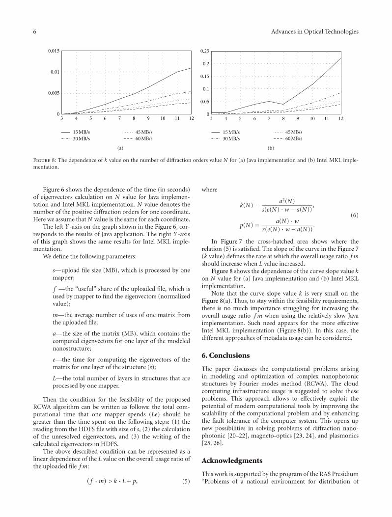
Figure 8: The dependence of k value on the number of diffraction orders value N for (a) Java implementation and (b) Intel MKL imple-mentation.
Figure 6 shows the dependence of the time (in seconds)of eigenvectors calculation on N value for Java implemen-tation and Intel MKL implementation. N value denotes thenumber of the positive diffraction orders for one coordinate.Here we assume that N value is the same for each coordinate.
The left Y-axis on the graph shown in the Figure 6, cor-responds to the results of Java application. The right Y-axisof this graph shows the same results for Intel MKL imple-mentation.
We define the following parameters:
s—upload file size (MB), which is processed by onemapper;
f —the “useful” share of the uploaded file, which isused by mapper to find the eigenvectors (normalizedvalue);
m—the average number of uses of one matrix fromthe uploaded file;
a—the size of the matrix (MB), which contains thecomputed eigenvectors for one layer of the modelednanostructure;
e—the time for computing the eigenvectors of thematrix for one layer of the structure (s);
L—the total number of layers in structures that areprocessed by one mapper.
Then the condition for the feasibility of the proposedRCWA algorithm can be written as follows: the total com-putational time that one mapper spends (Le) should begreater than the time spent on the following steps: (1) thereading from the HDFS file with size of s, (2) the calculationof the unresolved eigenvectors, and (3) the writing of thecalculated eigenvectors in HDFS.
The above-described condition can be represented as alinear dependence of the L value on the overall usage ratio ofthe uploaded file fm:
(f ·m) > k · L + p, (5)
where
k(N) = a2(N)s(e(N) ·w − a(N))
,
p(N) = a(N) ·wr(e(N) ·w − a(N))
.
(6)
In Figure 7 the cross-hatched area shows where therelation (5) is satisfied. The slope of the curve in the Figure 7(k value) defines the rate at which the overall usage ratio fmshould increase when L value increased.
Figure 8 shows the dependence of the curve slope value kon N value for (a) Java implementation and (b) Intel MKLimplementation.
Note that the curve slope value k is very small on theFigure 8(a). Thus, to stay within the feasibility requirements,there is no much importance struggling for increasing theoverall usage ratio fm when using the relatively slow Javaimplementation. Such need appears for the more effectiveIntel MKL implementation (Figure 8(b)). In this case, thedifferent approaches of metadata usage can be considered.
6. Conclusions
The paper discusses the computational problems arisingin modeling and optimization of complex nanophotonicstructures by Fourier modes method (RCWA). The cloudcomputing infrastructure usage is suggested to solve theseproblems. This approach allows to effectively exploit thepotential of modern computational tools by improving thescalability of the computational problem and by enhancingthe fault tolerance of the computer system. This opens upnew possibilities in solving problems of diffraction nano-photonic [20–22], magneto-optics [23, 24], and plasmonics[25, 26].
Acknowledgments
This work is supported by the program of the RAS Presidium“Problems of a national environment for distribution of
Advances in Optical Technologies 7
scientific information and computing based on the develop-ment of GRID technology and modern telecommunicationsnetworks”, grant of Russian Federation President for Supportof Leading Scientific Schools NSh-4128.2012.9 and RFBRgrants nos. 10-07-00553, 11-07-00153, 11-07-12051-ofi-m-2011, and 11-07-13164-ofi-m-2011-RGD, state contract withMinistry of Education and Science no. 07.514.11.4055 at12.10.2011, program no. 5 of basic research for Nanotech-nology and Information Technology Department of RAS“Basic problems of physics and technology of epitaxial nano-structures and related devices”.
References
[1] M. A. Golub, N. L. Kazanskii, I. N. Sisakyan, and V. A. Soifer,“Computational experiment with plane optical elements,”Optoelectronics, Instrumentation, and Data Processing, no. 1,pp. 78–89, 1988 (Russian).
[2] N. L. Kazanskiy, Mathematical Simulation of Optical Systems,Samara State Aerospace University (SSAU), Samara, Russia,2005.
[3] N. L. Kazanskiy, P. G. Serafimovich, and S. N. Khonina, “Har-nessing the guided-mode resonance to design nanoopticaltransmission spectral filters,” Optical Memory & Neural Net-works (Information Optics), vol. 19, no. 4, pp. 318–324, 2010.
[4] D. L. Golovashkin and N. L. Kasanskiy, “Solving diffractiveoptics problems using graphics processing units,” OpticalMemory & Neural Networks (Information Optics), vol. 20, no.2, pp. 85–89, 2011.
[5] M. G. Moharam, D. A. Pommet, E. B. Grann, and T. K. Gay-lord, “Stable implementation of the rigorous coupled-waveanalysis for surface-relief gratings: enhanced transmittancematrix approach,” Journal of the Optical Society of America A,vol. 12, no. 5, pp. 1077–1086, 1995.
[6] E. N. Gystis and T. Gaylord, “Three-dimensional (vector)rigorous coupled-wave analysis of anisotropic grating diffrac-tion,” Journal of the Optical Society of America A, vol. 7, no. 8,pp. 1399–1419, 1990.
[7] P. Lalanne and G. M. Morris, “Highly improved convergenceof the coupled-wave method for TM polarization,” Journal ofthe Optical Society of America A, vol. 13, no. 4, pp. 779–784,1996.
[8] L. Li, “Use of Fourier series in the analysis of discontinuousperiodic structures,” Journal of the Optical Society of AmericaA, vol. 13, no. 9, pp. 1870–1876, 1996.
[9] E. A. Bezus, L. L. Doskolovich, and N. L. Kazanskiy, “Evanes-cent-wave interferometric nanoscale photolithography usingguided-mode resonant gratings,” Microelectronic Engineering,vol. 88, no. 2, pp. 170–174, 2011.
[10] E. A. Bezus, L. L. Doskolovich, and N. L. Kazanskiy, “Scatter-ing suppression in plasmonic optics using a simple two-layerdielectric structure,” Applied Physics Letters, vol. 98, no. 22,Article ID 221108, 3 pages, 2011.
[11] M. Armbrust, A. Fox, R. Griffith et al., “A view of cloud com-puting,” Communications of the ACM, vol. 53, no. 4, pp. 50–58,2010.
[12] S. G. Volotovskiy, N. L. Kazanskiy, P. G. Seraphimovich, andS. I. Kharitonov, “Distributed software for parallel calculationof diffractive optical elements on web-server and cluster,” inProceedings of the IASTED International Conference on Auto-mation, Control, and Information Technology (ACIT ’02), pp.69–73, ACTA Press, 2002.
[13] M. Snir, S. Otto, S. Huss-Lederman, D. Walker, and J.Dongarra, MPI-The Complete Reference. The MPI Core, vol.1 of The MPI Core, The MIT Press, Cambridge, Mass, USA,1998.
[14] J. Dean and S. Ghemawat, “MapReduce: a flexible dataprocessing tool,” Communications of the ACM, vol. 53, no. 1,pp. 72–77, 2010.
[15] J. Venner, Pro Hadoop, Springer, 2009.[16] V. V. Voevodin, “Mapping computational problems in com-
puter architecture,” Computational Methods and Program-ming, vol. 1, no. 2, pp. 37–44, 2000 (Russian).
[17] S. B. Popov, “Modeling the task information structure inparallel image processing,” Computer Optics, vol. 34, no. 2, pp.231–242, 2010 (Russian).
[18] V. A. Soifer, Ed., Computer Image Processing, Part I: Basic Con-cepts and Theory, VDM Verlag Dr. Mueller e.K., 2009.
[19] M. Born and E. Wolf, Principles of Optics, Pergamon Press,Oxford, UK, 1980.
[20] V. A. Soifer, “Nanophotonics and diffractive optics,” ComputerOptics, vol. 32, no. 2, pp. 110–118, 2008 (Russian).
[21] V. A. Soifer, V. V. Kotlyar, and L. L. Doskolovich, “Diffractiveoptical elements in nanophotonic devices,” Computer Optics,vol. 33, no. 4, pp. 352–368, 2009 (Russian).
[22] N. L. Kazanskiy, P. G. Serafimovich, S. B. Popov, and S. N.Khonina, “Using guided-mode resonance to design nano-optical spectral transmission filters,” Computer Optics, vol. 34,no. 2, pp. 162–168, 2010 (Russian).
[23] V. I. Belotelov, L. L. Doskolovich, and A. K. Zvezdin, “Extraor-dinary magneto-optical effects and transmission throughmetal-dielectric plasmonic systems,” Physical Review Letters,vol. 98, no. 7, Article ID 077401, 4 pages, 2007.
[24] D. A. Bykov, L. L. Doskolovich, V. A. Soifer, and N. L. Kazan-skiy, “Extraordinary magneto-optical effect of a change in thephase of diffraction orders in dielectric diffraction gratings,”Journal of Experimental and Theoretical Physics, vol. 111, no. 6,pp. 967–974, 2010 (Russian).
[25] E. A. Bezus, L. L. Doskolovich, N. L. Kazanskiy et al., “Thedesign of the diffractive optical elements to focus surface plas-mons,” Computer Optics, vol. 33, no. 2, pp. 185–192, 2009(Russian).
[26] E. A. Bezus, L. L. Doskolovich, N. L. Kazanskiy, V. A. Soifer,and S. I. Kharitonov, “Design of diffractive lenses for focusingsurface plasmons,” Journal of Optics, vol. 12, no. 1, Article ID015001, 7 pages, 2010.

International Journal of
AerospaceEngineeringHindawi Publishing Corporationhttp://www.hindawi.com Volume 2010
RoboticsJournal of
Hindawi Publishing Corporationhttp://www.hindawi.com Volume 2014
Hindawi Publishing Corporationhttp://www.hindawi.com Volume 2014
Active and Passive Electronic Components
Control Scienceand Engineering
Journal of
Hindawi Publishing Corporationhttp://www.hindawi.com Volume 2014
International Journal of
RotatingMachinery
Hindawi Publishing Corporationhttp://www.hindawi.com Volume 2014
Hindawi Publishing Corporation http://www.hindawi.com
Journal ofEngineeringVolume 2014
Submit your manuscripts athttp://www.hindawi.com
VLSI Design
Hindawi Publishing Corporationhttp://www.hindawi.com Volume 2014
Hindawi Publishing Corporationhttp://www.hindawi.com Volume 2014
Shock and Vibration
Hindawi Publishing Corporationhttp://www.hindawi.com Volume 2014
Civil EngineeringAdvances in
Acoustics and VibrationAdvances in
Hindawi Publishing Corporationhttp://www.hindawi.com Volume 2014
Hindawi Publishing Corporationhttp://www.hindawi.com Volume 2014
Electrical and Computer Engineering
Journal of
Advances inOptoElectronics
Hindawi Publishing Corporation http://www.hindawi.com
Volume 2014
The Scientific World JournalHindawi Publishing Corporation http://www.hindawi.com Volume 2014
SensorsJournal of
Hindawi Publishing Corporationhttp://www.hindawi.com Volume 2014
Modelling & Simulation in EngineeringHindawi Publishing Corporation http://www.hindawi.com Volume 2014
Hindawi Publishing Corporationhttp://www.hindawi.com Volume 2014
Chemical EngineeringInternational Journal of Antennas and
Propagation
International Journal of
Hindawi Publishing Corporationhttp://www.hindawi.com Volume 2014
Hindawi Publishing Corporationhttp://www.hindawi.com Volume 2014
Navigation and Observation
International Journal of
Hindawi Publishing Corporationhttp://www.hindawi.com Volume 2014
DistributedSensor Networks
International Journal of