reliability analysis and sfg modeling of a new modified
TRANSCRIPT

3
Original scientific paper
MIDEM Society
Reliability analysis and SFG modeling of a new modified Quadratic boost DC-DC converter J. Divya Navamani, K. Vijayakumar, R. Jegatheesan, A. Jason Mano Raj
SRM University, Kattankulathur, India
Abstract: In the present scenario, direct current boost converters play a vital role in automobiles and various industries. The direct current boost converters are designed by diverse topologies in which every topology has its benefits. The task arises in developing a converter with reduced losses, increased efficiency, robust and high gain. In this paper, a novel topology for the DC-DC conversion is proposed for high-intensity discharge lamps. The designed topology is the modified structure of the quadratic boost converter and hence named as the modified quadratic boost converter. The model, which is proposed, is more efficient with increased performance. This model is compared with an existing model, and the results are verified. The open loop small-signal analysis of the proposed topology is carried out using the switching flow graph modeling method to perform the dynamic analysis. The reliability analysis of the converter introduced is done for ensuring the lifetime operation of the converter. From reliability analysis, it is observed that the proposed topology is 14 years more reliable than the compared existing topology. It is also identified that the derived one is 6% more efficient than the compared one. A 40 W prototype, which is suitable for HID lamps, is developed to validate the theoretical results.
Keywords: MQB (Modified Quadratic Boost); voltage stress; efficiency; SFG (Switching Flow Graph); frequency domain; reliability
Zanesljivostna analiza in SFG modeliranje novega modificiranega kvadratičnega DC-DC pretvornika navzgorIzvleček: Direktni pretvorniki navzgor danes predstavljajo pomembno vlogo v industriji. Realizirani so v različnih topologijah. V članku je predlagana nova topologija DC-DC pretvornika za uporabo v visokotlačnih sijalkah. Predlagana topologija sloni na kvadratičnem pretvorniku navzgor z izboljšanim izkoristkom in učinkovitostjo. Rezultati so preverjeni in primerjani z obstoječim modelom. Odprtozančna analiza majhnih signalov je opravljena na osnovi je opravljena z modelom grafa preklopnega poteka. Zanesljivostna analiza je pokazala, da je zanesljivostna doba predlagane topologije 14 let daljša od obstoječe topologije. Teorija je verificirana na osnovi idealnega prototipa moči 40 W, ki je primeren za napajanje HID sijalk.
Ključne besede: kvadratičen pretvornik; napetostni stres; izkoristek; SFG; frekvenčna domena; zanesljivost
* Corresponding Author’s e-mail: [email protected]
Journal of Microelectronics, Electronic Components and MaterialsVol. 48, No. 1(2018), 3 – 18
1 Introduction
In the present generation, high gain DC-DC converters find their application in various fields. Due to power cri-sis and shortage of electricity generations, the efficient use of the available energy in the present scenario plays a significant role [16]. In this case, DC- DC boost converters play a major role in renewable power plants. There are various topologies for the DC-DC boost con-verters with different drawbacks such switch voltage stress, losses in the nonlinear elements, very less volt-age gain and so on. The methods to achieve high step-
up, low cost, and high-efficiency DC-DC conversion constitute a significant consideration. The high-inten-sity discharge lamps are used in automobiles, which are powered by the batteries at low voltage. Hence, it is needed to step-up the voltage to the high level of output voltage. The operating voltage of the HID lamps is 80-90 V which cannot be achieved by conventional boost converter with 12 V supply. To achieve a highly efficient DC-DC boost conversion with reduced losses and high voltage gain, the below model is proposed with reduced number of inductors compared to the model considered for the comparison.

4
J. Divya Navamani et al; Informacije Midem, Vol. 48, No. 1(2018), 3 – 18
Various topologies had been constructed in the recent years to achieve high voltage gain for numerous ap-plications. There are several methods to produce the high gain in DC-DC converters. Voltage multiplier cell, switched capacitor, switched inductor, voltage-lift cell, coupled inductor is integrated with the conventional DC-DC topologies to boost the voltage conversion ra-tio. Cockcroft and Dickson multiplier cells are used to boost the voltage of the converters. Dickson and Cock-croft multiplier cell are incorporated in the boost con-verter, and their performance is analyzed in [1, 2]. The gain of the converter is further increased by the add-ing coupled inductor to the topology, and it is reported in [3]. This leads to increase in the number of compo-nents. Boost converter integrated coupled inductors are reported in the literature [4, 5]. However, the use of multiple coupled inductors complicates the dynamic analysis of those topologies [6]. Ultra gain converters are derived by voltage lift cells which are introduced by F.L. Luo [7, 8]. However, high gain is achieved with self and relift techniques with too many components[15]. Two or more methods are integrated to attain high voltage gain and combine its advantages for better performance. The coupled inductor is combined with switched capacitor cell to derive high step-up convert-er, and quasi-resonant operation is employed to reduce the switching loss [9, 10]. Asymmetrical and symmetri-cal hybrid switched inductor converters are proposed in [11] for PV grid connected system. However, the above-mentioned topologies are derived by adding additional components to the existing converters. In this paper, we have derived a high gain converter with the simple modification in the conventional topology. The primary objective of the work is to design a DC-DC boost converter, which is more efficient in conversion with much-reduced losses, compared with an existing converter and must be suitable for meeting the re-quirements of high-intensity discharge lamps.
The variation in the derived topology presented in this paper is the alteration of the existing converter, i.e., Quadratic boost converter with the addition of only one capacitor and a removal of a diode [12]. The maxi-mum stress voltage across all the components in the modified topology is found to be lower compared to the quadratic boost converter. The proposed topol-ogy is compared with quadratic boost converter and existing converter in the literature. Mostly, compara-tive study will be based on efficiency, voltage stress, volume, and reliability. We have compared the pro-posed topology with the existing topology based on reliability using FIDES guide [13]. The superiority of the proposed topology is proved based on the reliability, which is not reported in the literature until now.
The paper is organized as follows: Section 2 provides the modes of operation of the proposed topology. Sec-tion 3 gives steady-state analysis in CCM and DCM con-dition, the design of passive components, efficiency analysis, time domain and frequency domain analysis. The proposed topology is evaluated with the existing converters, and it is presented in section 4. Reliability study is performed on proposed topology and com-pared with the existing topology, and it is shown in section 5. Section 6 presents the simulation results to provide evidence to the theoretical calculation, and a prototype is raised to confirm the derived topology. Fi-nally, the paper is terminated in section 7.
2 Structure of proposed converter
Figure 1(a) and (b) present the conventional quadratic boost converter and modified quadratic boost con-verter as proposed topology respectively. The modifi-cation made in the existing quadratic boost converter is the removal of one diode and addition of capacitor. The total number of devices in both the converters is same with the single switch. A number of passive com-ponents in quadratic boost converter are four, and it is five in the proposed topology. The diode count in the proposed converter is two, but it is three in the quad-ratic boost converter. The converter mainly comprises of two inductors, three capacitors, two diodes, resistive load, and a switch. The advantage of the modification made in the topology is discussed in section 4. Figure 2 (a) and (b) provide the mode 1 and mode 2 of the proposed topology.
Figure 1: (a) Quadratic boost converter (b) Proposed topology
(a)
(b)

5
Figure 2: (a) Mode 1 (b) Mode 2
Mode 1: The states of device conduction and current path for the conducting state of the S are given in Fig-ure 2(a). When switch SW is ON, inductor L1 and L2 are charged to the supply voltage Vg. Diode D1 is reverse biased by the negative polarity of the supply voltage through the switch. Diode Do also reverse biased by the voltage across the inductor L2. Load voltage is due to the charge in the output capacitor.
Mode 2: Figure 2(b) gives the current path when the switch S is in non-conducting state. Diode D1 and DO are forward biased due to the voltage of the capaci-tor. The inductor L1 and L2 started to discharge through these diodes. The output voltage is equal to the sum-mation of the input voltage, capacitor C1 and C2 volt-age. Figure 3 gives the current through all the passive components and diode.
3. Analysis of the proposed topology
3.1 Steady State Analysis in CCM
Voltage across the inductor L1 and L2 in ON and OFF mode is written as follows
L1 g
V V= (1)
L2 g C1 C2
V V V V= + − (2)
L1 C1
V V= − (3)
L2 C2
V V= − (4)
By applying volt-sec balance principle to the Equations (1)-(4), capacitor voltage C1 and C2 is obtained as
g
C1 C2
V DV V
1 D= =
− (5)
The output voltage is given as
O g C1 C2
V V V V= + + (6)
By simplifying the Equation (6), the voltage gain of the converter is obtained as
[ ]2
O
VCCM 2
g
V 1 DG
V 1 D
−= =−
(7)
Current through the capacitor C1 and C2 is written and by applying charge-sec balance principle, the current through the inductor L1 and L2 is obtained as
(a)
(b)
Figure 3: Current waveforms of the MQB converter
J. Divya Navamani et al; Informacije Midem, Vol. 48, No. 1(2018), 3 – 18
6
2
g g
L1 L2
L L
V V1 D 1 DI ; I
1 D R 1 D R
+ + = = − − (8)
3.2 Boundary Conditions for Inductor L1 and L
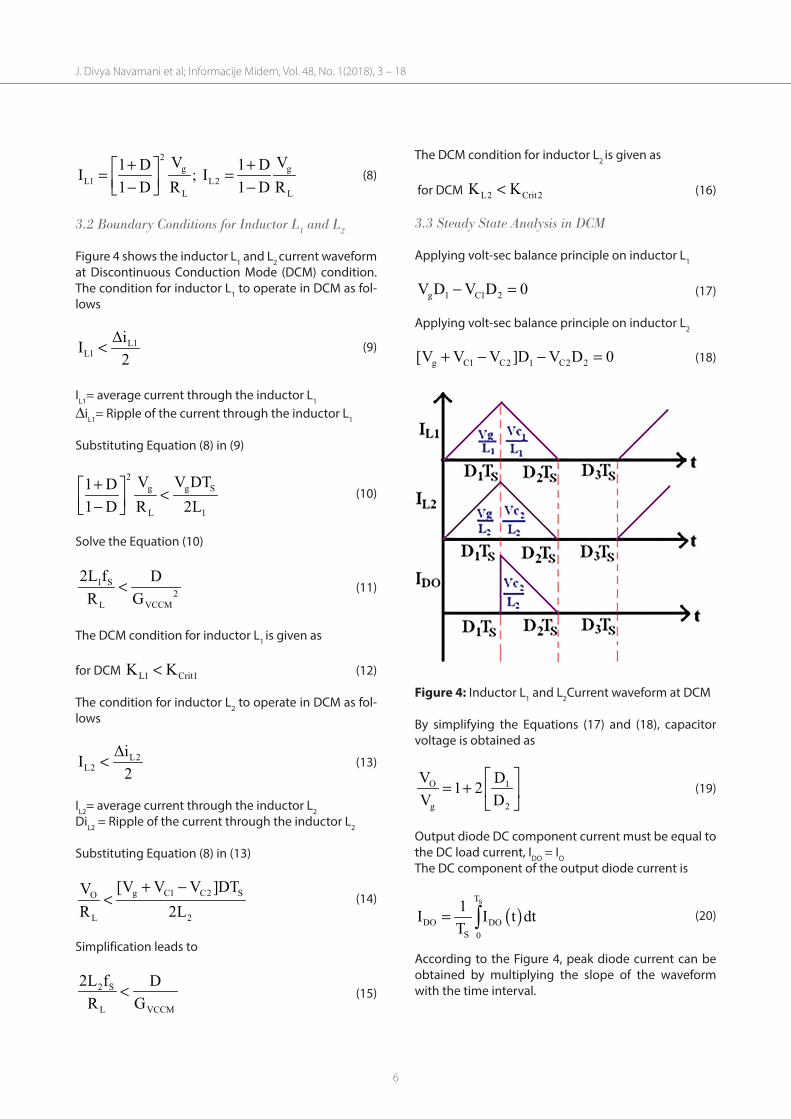
2
Figure 4 shows the inductor L1 and L2 current waveform at Discontinuous Conduction Mode (DCM) condition. The condition for inductor L1 to operate in DCM as fol-lows
L1
L1
ΔiI
2< (9)
IL1= average current through the inductor L1
DiL1= Ripple of the current through the inductor L1
Substituting Equation (8) in (9)
2
g g S
L 1
V V DT1 D
1 D R 2L
+ < − (10)
Solve the Equation (10)
1 S
2
L VCCM
2L f D
R G< (11)
The DCM condition for inductor L1 is given as
for DCM L1 Crit1
K K< (12)
The condition for inductor L2 to operate in DCM as fol-lows
L2
L2
ΔiI
2< (13)
IL2= average current through the inductor L2DiL2 = Ripple of the current through the inductor L2
Substituting Equation (8) in (13)
g C1 C2 SO
L 2
[V V V ]DTV
R 2L
+ −< (14)
Simplification leads to
2 S
L VCCM
2L f D
R G< (15)
The DCM condition for inductor L2 is given as
for DCM L2 Crit2
K K< (16)
3.3 Steady State Analysis in DCM
Applying volt-sec balance principle on inductor L1
g 1 C1 2
V D V D 0− = (17)
Applying volt-sec balance principle on inductor L2
g C1 C2 1 C2 2
[V V V ]D V D 0+ − − = (18)
Figure 4: Inductor L1 and L2Current waveform at DCM
By simplifying the Equations (17) and (18), capacitor voltage is obtained as
O 1
g 2
V D1 2
V D
= +
(19)
Output diode DC component current must be equal to the DC load current, IDO = IOThe DC component of the output diode current is
( )
ST
DO DO
S 0
1I I t dt
T= ∫ (20)
According to the Figure 4, peak diode current can be obtained by multiplying the slope of the waveform with the time interval.
J. Divya Navamani et al; Informacije Midem, Vol. 48, No. 1(2018), 3 – 18

7
Simplify the integral (20) and rearrange to yield
O 1 2 S L
g 2
V D D T R
V 2L= (21)
Solving the Equations (19) and (21) yield the voltage conversion ratio of the proposed topology in DCM
2
1
L2O
VDCM
g
8D1 1
KVG
V 2
± += =
(22)
The complete modified quadratic boost converter’s conversion ratio including CCM and DCM are
[ ]2
2
2V
L2
1 D . ..
1 D
G8D
1 1K
..2
CCM
DCM
− …… ……… −= ± +
…………
(23)
3.4 Design of Inductor and Capacitor
Current ripple, voltage ripple, and switching frequency are required to design the passive elements of the con-verter. The peak-to-peak current ripple of Inductor L1 and L2 is given as
( ) ( )( )
L1 O
L1
1 S
i DT V 1 D DI
2 2 1 D L f
∆ −= =
+ (24)
( ) ( )( )
L2 O
L2
2 S
i DT V 1 D DI
2 2 1 D L f
∆ −= =
+ (25)
Using Equation (8), the design equation of Inductor L1 and L2 is obtained as
( )( )
( )( )
2
L L
1 22
SS
1 D DR 1 D DRL ; L
2 1 D f2 1 D f
− −= =
++ (26)
The peak to peak voltage ripple of capacitor C1, C2 and CO is calculated and rearranged to yield the design equations of the capacitor
O O O
1 2 0
C1 S C2 S CO S
I D I D I DC ; C ; C
V f V f V f= = =
∆ ∆ ∆ (27)
3.5 Power loss and Efficiency analysis
The power losses and efficiency of the proposed topol-ogy are calculated by considering parasitic resistance, diode threshold voltage, and on-state resistance of the switch. In this calculation, RL1, RL2 is the ESR of the in-ductor, RC1, RC2 and RCO are the ESR of the capacitor, RDS and RF are the on-state resistance of the switch and di-ode respectively. VF is the diode threshold voltage.
RMS value of switch current:
( )
L1 L2
S RMS
I I 0
I
0 .
t DT
DT t T
+ …… < <= …… < <
(28)
( )[ ][ ]
DT2
L1 L2 g0
S RMS 2
L
I I dt 2 D 1 D VI
T R 1 D
+ += =
−∫
Similarly, average and RMS currents of diodes are ob-tained as
( ) ( ) OD1 avg D2 avgI I I= = (29)
( ) ( )
O
D1 RMS D2 RMS
II I
1 D= =
− (30)
RMS value of capacitor current:
( ) ( ) ( ) OC1 RMS C2 RMS C3 RMS
1 DI I I I
1 D
+= = =−
(31)
RMS values of the inductor currents are taken from Equation (8).
Total losses of the converter = L SW D C
P P P P+ + +
(32)
out
out loss
PEfficiency η
P P= =
+ (33)
J. Divya Navamani et al; Informacije Midem, Vol. 48, No. 1(2018), 3 – 18

8
3.6 Time domain and Frequency domain Analysis
3.6.1 Time domain analysis.
The important objective of investigating the time do-main and frequency domain analysis of a converter is
to design a control system. The desired requirement of the system can be attained by an appropriate design of control system. The converter taken for comparison combines the features of impedance source converter and quadratic boost converter [11]. This topology is derived to achieve high voltage gain. However, it can operate only with D<0.5 as positive output converter. Figure 5 gives the responses of the proposed topol-ogy and quasi Z source topology [11], which is taken for comparison. It is observed in Figure (a)-(d), the pro-posed topology has excellent settling time and less overshoot compared to the quasi Z source topology. The settling time of the proposed topology is just 42% of the converter taken for comparison, and the results are presented in Figure 5(c) and (d). The time domain analysis of both the converter explains the time re-sponse of the proposed converter, which takes less time for stable operation than the compared converter.
3.6.2 Frequency domain analysis.
To simplify the analysis, output capacitor of the con-verter is not considered. Order of the system is four. Figure 6 provides the signal flow graph of the MQB converter for small signal analysis.
Figure 6: Small-signal analysis of MQB converter
Averaged and linearised state equations are derived using steady-state analysis to develop signal flow graph. By adding perturbation to the linearised equa-tion, the AC equations are used to draw the signal flow graph[17]. Individual loop and non-touching loop gains are identified from the figure 6. Finally, forward path gains are traced to apply mason’s gain formula to derive the transfer function.
Table 1 presents the values of the circuit parameters used for transfer function calculation to perform fre-quency domain analysis. Table 2 furnishes the com-plete frequency domain analysis of the proposed to-pology and the transfer functions are also provided in the table.The root locus diagram for input to output
Figure 5: Time domain analysis (a) Output voltage of MQB converter for the step change in input.(b) Output voltage of Quasi Z source topology for the step change in input. (c) Settling time and maximum overshoot of MQB converter (d) Settling time and maximum over-shoot of Quasi Z source topology
(a)
(b)
(c)
(d)
J. Divya Navamani et al; Informacije Midem, Vol. 48, No. 1(2018), 3 – 18

9
Table 1: Circuit parameters for frequency domain analysis of the proposed topology
Po(W) Vg(V) Vo(V) Ro(Ω) fs(kHz) L1(uH) L2(uH) C1(uF) C2(uF) Co(uF)40 24 96 230 60 72 287 10 10 5
Table 2: Loops and their gains-SFG
Loops(L) Loop gains Non-touching loop gain
1 L1 C1 C1 L1 L1
L s v s i v i i= → → → →
) ) ) ) ) O
D2rms DOrms
I 1 DI I
1 D
−= =
−
1 2 4
1 2 1 2
D'L L
S L L C C
−=
2 L2 C2 C2 L2 L2
L s v s i v i i= → → → →
) ) ) ) ) 2 2
2 2
1L
S L C
−=
1 5 3
1 1 2 O
D'L L
S L C C R
−=
) 3 C1 L2 L2 C2 C2 O C1 C1
L s s v s vv i i v v v= → → → → → → →
) ) ) ) ) ) )
[ ][ ]3 3
2 1 2 O
D 1 DL
S L C C R 1 D
+=
− [ ]
[ ]2 4 3
2 2 1 O
1 DL L
S L C C R 1 D
− +=
−
) 4 C1 O C1 C1
L s vv v v= → → →) ) )
[ ][ ]4
1 O
1 DL
SC R 1 D
+=
−
5 C2 O C2 C2
L s vv v v= → → →
) ) ) )
5
2 O
1L
SC R
−=
Input to output transfer function
Forward paths(FP) from
) g O v v→
)
Gain
g L1 L1 C1 C1 O
v s i i s v v v→ → → → →
) ) ) ) ) ) g1 2
1 1
DFP
S L C
−=
g O v v→
) ) g2
FP = 1
) g L2 L2 C2 C2 O
v s i i s v v v→ → → → →
) ) ) )) g3 2
2 2
DFP
S L C=
) g L1 L1 C1 C1 L2 L2 C2 C2 O
v s i i s v v s i i s v v v→ → → → → → → → →
)) ) ) ) ) ) ) ) 2
g4 4
1 1 2 2
DFP
S L C L C
−=
Transfer function:
Control to output transfer function
Forward paths(FP) from
)
O d v→
))
Gain
) L2 L2 C2 C2 O
d s i i s v v v→ → → → →
) ) ) ))
[ ]g
g1 2
2 2
VFP
S 1 D L C=
−
) L1 L1 C1 C1 L2 L2 C2 C2 O
d s i i s v v s i i s v v v→ → → → → → → → →
) ) ) ) ) ) ) ))
[ ]g
g2 4
1 1 2 2
VFP
S 1 D L C L C
−=
−
L1 L1 C1 C1 O
d s i i s v v v→ → → → →
) ) ) ) ))
[ ]g
g3 2
1 1
VFP
S 1 D L C
−=
−Transfer function:
( )( )
[ ] [ ] g1 1 g2 g3 2O
1 2 3 4 5 1 2 1 5 2 4
FP 1 L FP FP 1 Ls
1 L L L L L L L L L L Ld s
gK KFPv ∆ − + + −= =
∆ − − − − − + + +∑
))
J. Divya Navamani et al; Informacije Midem, Vol. 48, No. 1(2018), 3 – 18

10
and control to output transfer function are shown in Figure 7(a) and (c) respectively. Magnitude and phase plot for both the derived transfer functions are given in Figure 7(b) and (d) . From root locus in Figure 7(a), it is observed that the input to output transfer function has two complex poles and zeros and two real poles and zeros. One real pole and zero lie in the right half of the s-plane. Similarly, the control to output transfer function has two complex poles, two complex zeros and two real poles.One real pole lies in the right half of the s-plane. The status of pole-zero locations is given in Table 3.
By investigating the bode diagram of ( ) ( )gOV s / V s , it
is understood that the magnitude curve of the function starts with a gain of 7.62 dB at 1.02X10³ rad/sec and the magnitude curve slope becomes -40 dB/dec. The phase curve has a phase reduction of -180°, so the curve re-duced from 360° to 180°. Similarly, the magnitude and phase plot continue accordingly to the values of poles and zeros. Due to the presence of zero in the right of the s-plane and low value of phase margin, the system exhibits non-minimum phase behavior. Bode plot of the duty cy-cle to output transfer function is similar to previous trans-fer function bode plot except the phase margin is 0.0237°.
4 Advantages of the proposed converter
The proposed topology is compared with the quadratic boost converter and quasi Z source topology proposed in [11]. Even though the gain of the proposed convert-
Table 3: Poles and zeros of the open loops transfer function
Input to output transfer functionPoles and zeros Values Damping Overshoot (%) Frequency (rad/sec)
Poles(4)
2.6x10⁴ -1 0 2.6x10⁴
-416+1.87x10⁴i 0.0223 93.2 1.87x10⁴
-416-1.87x10⁴i 0.0223 93.2 1.87x10⁴
-2.25x10⁴ 1 0 2.25x10⁴
Zeros(4)
3.12x10⁴ -1 0 3.12x10⁴
-2.18x10⁴i 0 100 2.18x10⁴
+2.18x10⁴i 0 100 2.18x10⁴
-3.12x10⁴ 1 0 3.12x10⁴
Control to output transfer functionPoles and zeros Values Damping Overshoot (%) Frequency (rad/sec)
Poles(4)
2.6x10⁴ -1 0 2.6x10⁴
-416+1.87x10⁴i 0.0223 93.2 1.87x10⁴
-416-1.87x10⁴i 0.0223 93.2 1.87x10⁴
-2.25x10⁴ 1 0 2.25x10⁴
Zeros(2)3.05x104 x104i 0 100 3.05x10⁴
-3.05x104 x104i 0 100 3.05x10⁴
er is less compared to the quadratic boost converter for the same duty cycle, MQB converter’s performance is superior compared to other two converters taken for the same power and voltage rating. Table 4 gives all the theoretical formula derived for the proposed topol-ogy and is tabulated along with the quasi z-source and the quadratic boost converter. Figures 8(a)-(d) furnish-es the comparative graphs of the MQB converter with other converter taken for comparison. Figure 8(b) en-dows the capacitor voltage stress for different output voltage rating. The proposed converter has very low buffer capacitor stress compared to another converter.
Switch and diode voltage stress is determined using switch utilization (SUF) and diode utilization factor (DUF)
rated
n
M MM 1
PSUF or DUF
V I=
=∑ (34)
Where VM = voltage stress across the switch or diode.
IM = current stress through the switch or diode.
Switch and diode utilization factors are calculated us-ing the equation (34). From the Figure 8(c), it is ob-served that the SUF of the MQB converter is 1.7 and 2.7 times of the quadratic boost and quasi z-source topol-ogy respectively. Similarly, from the Figure 8(d), it is de-tected that the DUF of the MQB converter is 1.8 and 4.7 times of the quadratic boost and quasi z-source topol-
J. Divya Navamani et al; Informacije Midem, Vol. 48, No. 1(2018), 3 – 18

11
Figure 7: Frequency domain analysis (a) Root locus diagram of input to output transfer function (b) bode plot of input to output transfer function (c) Root locus diagram of control to output transfer function (d) bode plot of control to output transfer function
(a)
(b)
(c)
(d)
Figure 8: (a) Output voltage Vs switch voltage stress (b) Output voltage Vs capacitor voltage stress (c) Output voltage Vs switch utilization factor (d) Output voltage Vs diode utilization factor
(a)
(b)
(c)
(d)
J. Divya Navamani et al; Informacije Midem, Vol. 48, No. 1(2018), 3 – 18

12
Table 4: comparison of proposed converter with existing topology
Sno Parameter Proposed Topology Quadratic boost converter Quasi Z-source topology[11]
1 Voltage gain
( )2
2
1 D
1 D
−−
[ ]2
1
1 D− 1
1 2D−
2 Inductor design
[ ][ ]
2
O
1 2
S
R 1 D DL
2 1 D f
−=
+
[ ][ ]
O
2
S
R 1 D DL
2 1 D f
−=
+
[ ]4
O
1
S
R 1 D DL
2f
−=
[ ]3
O
2
S
R 1 D DL
2f
−=
[ ]2
O
1
S
R 1 2D DL
2f
−=
[ ][ ]
O
2
S
R 1 2D DL
2 1 D f
−=
−
[ ]O
3
S
R 1 2DL
2f
−=
3 Switch voltage stress
g
V
1 D−
OV
[ ]gV 1 D
1 2D
+−
4 Switch current stress
O2 DI
1 D−
[ ][ ]
O
2
2 D DI
1 D
−−
O2 DI
1 2D−
5 Diode current stress
O
D1rms DOrms
II I
1 D= =
−
[ ]O
D1rms 2
I DI
1 D=
−
O
D2rms DOrms
I 1 DI I
1 D
−= =
−
O
D1rms D3rms
I 1 DI I
1 2D
−= =
−
O
D1rms
I DI
1 2D=
−
6 Capacitor Volt-age stress
g
C1 C2
V DV V
1 D= =
−
g
C1
VV
1 D=
−
g
C1
VV
1 D=
−
[ ][ ]g
C2
V DV
1 D 1 2D=
− −
7 Diode voltage stress
g
D1 DO
VV V
1 D= =
−
g
D1 D2
VV V
1 D= =
−
DO OV V=
g
D1
VV
1 D=
−
[ ][ ]g
D2
2DVV
1 D 1 2D=
− −
[ ][ ]g
D3
VV
1 D 1 2D=
− −
8 Total device count
3-Diode;1-Switch; 2-Induc-tor
2-Capacitor
2-Diode;1-Switch2-Inductor; 3-Capacitor
3-Diode;1-Switch;3-Inductor; 2-Capacitor
SUF(Switch Utilization Factor)(PO = 40 W, Vg = 24 V, VO = 96 V)9 SUF 0.412 0.235 0.148
DUF(Diode Utilization Factor)( PO = 40 W, Vg = 24 V, VO = 96 V)10 DUF 0.505 0.282 0.107
ogy respectively. The proposed converter is also com-pared with the converter in [14]. It is observed that the
gain of the converter in [14] is just similar to the pro-posed converter. The converter [14] achieves the same
J. Divya Navamani et al; Informacije Midem, Vol. 48, No. 1(2018), 3 – 18
13
voltage conversion ratio with four capacitors whereas, with the proposed topology, it is three capacitors. The MQB converter possesses a total component count of 8 whereas the converter [14] has nine devices with 3- diodes, 4- capacitors, 2-inductors and a switch. Switch voltage stress in both the converters is observed to be same and it is measured by the equation Vg/[1-D].
5 Reliability study of the proposed converter
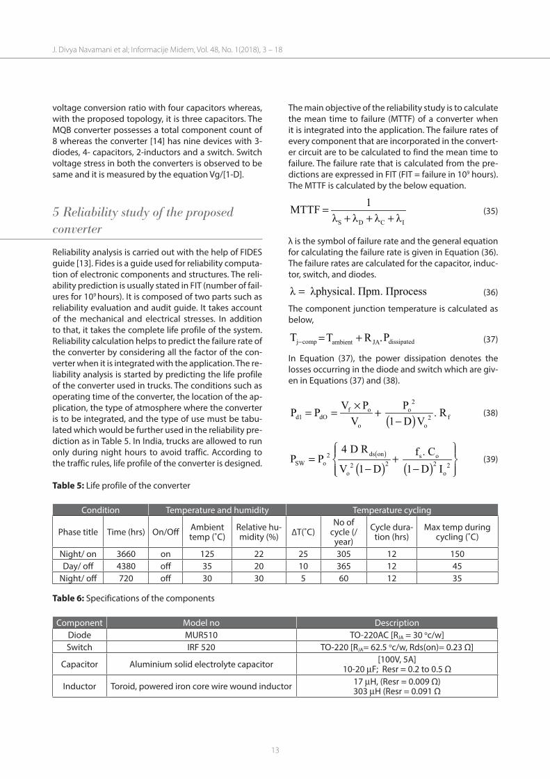
Reliability analysis is carried out with the help of FIDES guide [13]. Fides is a guide used for reliability computa-tion of electronic components and structures. The reli-ability prediction is usually stated in FIT (number of fail-ures for 109 hours). It is composed of two parts such as reliability evaluation and audit guide. It takes account of the mechanical and electrical stresses. In addition to that, it takes the complete life profile of the system. Reliability calculation helps to predict the failure rate of the converter by considering all the factor of the con-verter when it is integrated with the application. The re-liability analysis is started by predicting the life profile of the converter used in trucks. The conditions such as operating time of the converter, the location of the ap-plication, the type of atmosphere where the converter is to be integrated, and the type of use must be tabu-lated which would be further used in the reliability pre-diction as in Table 5. In India, trucks are allowed to run only during night hours to avoid traffic. According to the traffic rules, life profile of the converter is designed.
Table 5: Life profile of the converter
Condition Temperature and humidity Temperature cycling
Phase title Time (hrs) On/Off Ambient temp (˚C)
Relative hu-midity (%) ∆T(˚C)
No of cycle (/
year)
Cycle dura-tion (hrs)
Max temp during cycling (˚C)
Night/ on 3660 on 125 22 25 305 12 150Day/ off 4380 off 35 20 10 365 12 45
Night/ off 720 off 30 30 5 60 12 35
The main objective of the reliability study is to calculate the mean time to failure (MTTF) of a converter when it is integrated into the application. The failure rates of every component that are incorporated in the convert-er circuit are to be calculated to find the mean time to failure. The failure rate that is calculated from the pre-dictions are expressed in FIT (FIT = failure in 109 hours). The MTTF is calculated by the below equation.
S D C I
1MTTF
λ λ λ λ=
+ + + (35)
λ is the symbol of failure rate and the general equation for calculating the failure rate is given in Equation (36). The failure rates are calculated for the capacitor, induc-tor, switch, and diodes.
λ λphysical . Πpm . Πprocess = (36)
The component junction temperature is calculated as below,
j comp
T − ambient JA
T R+ dissipated
P= . (37)
In Equation (37), the power dissipation denotes the losses occurring in the diode and switch which are giv-en in Equations (37) and (38).
( )2
f o o
d1 dO f2
o o
V P PP P . R
V 1 D V
×= = +
− (38)
( )
( ) ( )ds on2 s o
SW o 2 22 2
o o
4 D R f . CP P
V 1 D 1 D I
= + − −
(39)
Table 6: Specifications of the components
Component Model no DescriptionDiode MUR510 TO-220AC [RJA = 30 oc/w]Switch IRF 520 TO-220 [RJA= 62.5 oc/w, Rds(on)= 0.23 Ω]
Capacitor Aluminium solid electrolyte capacitor [100V, 5A] 10-20 mF; Resr = 0.2 to 0.5 Ω
Inductor Toroid, powered iron core wire wound inductor 17 mH, (Resr = 0.009 Ω)303 mH (Resr = 0.091 Ω
J. Divya Navamani et al; Informacije Midem, Vol. 48, No. 1(2018), 3 – 18

14
The Table 6 shows the specifications of the components that are selected. From the stress values and the base failure rate values of the components, the failure rate value is calculated and tabulated in Table 7 along with the failure rate values of the compared quazi z source converter, which is calculated similarly.
Table 7: Failure rate values of components
Failure Rate Proposed MQB Converter
Compared Quazi z converter
lS 384.04 451.1853
lD 2863.92 5037
lI 3.026 4.539
lC 101.304 110.4
The above failure rate values are used in the Equation (35) to calculate the mean time to failure of the con-verter which is given below.
For the proposed modified quadratic dc-dc boost con-verter,
lS + lD + lC + lI = 3352.2787 FIT
MTTF = 34.05 years
For the compared quadratic quazi z source converter,
lS + lD + lC + lI = 5603.1243 FIT
MTTF = 20.37 years
Thus from the reliability analysis, the mean time to fail-ure is calculated. When comparing both the converters, the proposed modified quadratic boost converter can work without failure for nearly 14 year more than the compared converter due to the lesser number of com-ponent counts and reduced losses in the components. While including the controller circuit and the gate driver circuit the value might vary depending upon the methods used.
Table 8: Components of hardware circuit
Parameters Components
Input voltage 40 V Switch IRF520
Output power 40 W Diode MUR510
Switching frequency 20 kHz Inductor 400 uH, 1 mH
Output voltage 93 V Capacitor 10 uF
Duty cycle 0.4 dsPIC Controller dsPIC33FJ64MC802
Gate driver circuit IRS2110
6 Simulation and experimental results
Simulation is carried out with Tina software and pre-sented in the Figures 9(a)-(g). The proposed topology is simulated in Tina design suite TI version 9. The circuit response to the input voltage is calculated in the tran-sient and mixed mode of Tina. In a transient analysis, the DC operating point can be calculated which is used to check with the theoretical results obtained from the steady-state analysis. By comparing the simulation re-sults and the theoretical results, the values are more satisfactory. The voltage across the inductors and ca-pacitors during turn ON and turn OFF period are same as that of the theoretical values. The calculated volt-age gain and capacitor voltage by volt-second balance principle are more accurate to the simulation results.(a) (b)
Figure 9(h) gives a pictorial representation of the ef-ficiency between the converters, in the form of the graph. The efficiency analysis of converter is carried out by estimating the losses in the conversion process. The losses are mainly due to switching frequency, power diodes, passive elements such as inductor and capaci-tors. The output power versus the efficiency is plotted, and we infer from the graph that the converter’s effi-ciency decreases with increase in the power ratings, but the rate of decrease in efficiency varies. The rate of decrease of the efficiency is less in proposed converter when compared to the compared converter. From the efficiency and loss analysis, it’s more obvious that the proposed converter is much dominant than the com-pared converter.
Figure 10 shows the hardware that is developed for the converter proposed. The dsPIC controller generates a switching pulse of 5 V amplitude and 20 kHz frequency. A power supply of 230 V is given to the transformer, which is stepped down to 15 V and 40 V respectively. 15 V is given to the dsPIC controller kit, and 40 V is given to the bridge rectifier circuit. The rectifier converts the 40 V AC to 40 V DC, which is given to the converter for input supply. The 15 V AC is again stepped down to 5 V
J. Divya Navamani et al; Informacije Midem, Vol. 48, No. 1(2018), 3 – 18

15
Figure 9: Simulation results (a) Output and Switch voltage (b) Diode voltages (c) Capacitor voltages (d) Inductor cur-rents (e) Inductor voltages (f ) Switch and diode currents (g) Input and output currents (h) output power Vs Efficiency.
(a) (b)
(c) (d)
(e) (f )
(g)
(h)
J. Divya Navamani et al; Informacije Midem, Vol. 48, No. 1(2018), 3 – 18

16
as a power supply to the controller and the gate driver circuit. Table 8 gives the components and parameters used for the hardware circuits
The Figure 11(a) shows the switching pulse waveform generated from the dsPIC controller with 0.4 duty cy-cle. The ON time of the switch is hence 40 % and the OFF time is remaining 60%. Thus for that duty cycle, the boost ratio is 2.33 and the output voltage for 40 V input is 90 V. The Figure 11(b) shows the input and output waveforms of the converter. The input voltage given to the converter is 40 V and the output voltage of the con-verter is 90 V. The channel 2 shows the output voltage and the channel 1 shows the input voltage. The voltage across the switch connected to the converter model is taken between drain and source and given in Figure
11(c). Theoretically, by
g
V
1 D− the maximum switch voltage is 66 V, and it is observed that the hardware switch voltage is very close to the theoretical value. However, conventional quadratic boost converter has switch voltage stress equals to its output voltage. The proposed topology with low switch voltage stress uses low Rds(on) switches which reduces the cost of the com-ponent. A closer inspection shows that the hardware results validate the simulation and theoretical results. To increase the voltage gain, the coupled inductor can be incorporated. Thus, the proposed converter can be extended in the future for further increase in voltage conversion ratio.
7 Conclusion
The proposed topology for the operation of high-intensity discharge lamps has been described in this work. The same topology can be operated with PV source as an input. The converter is more suitable to
be operated for lower power ratings and the efficiency decrease slightly with the increase in the power ratings. The output response with variation of input supply is studied in open loop conditions. The attractive features of the MQB converter are:
It has low buffer capacitor voltage stress.
SUF of the proposed converter is approximately 2-3 times greater than that of the compared converter.
Figure 10: Photograph of the hardware
Figure 11: Experimental results (a) Gate pulse (Amp: 5 V/div; Time period: 10us/div) (b) Input and output volt-age (Input voltage: Ch1: Amp: 20V/div; Time period: 10us/div; Output voltage: Ch2: Amp: 20V/div; Time pe-riod: 10us/div) (c) Voltage across the switch
(a)
(b)
(c)
J. Divya Navamani et al; Informacije Midem, Vol. 48, No. 1(2018), 3 – 18

17
Similarly, DUF of the MQB converter is 2-5 times higher than the converter taken for comparison. SUF and DUF of the proposed topology are very high compared to another converter. Therefore, it allows us to choose low rating semiconductor devices and which results in low cost of the devices.
The efficiency of the proposed converter is 6% higher as that of the compared converter for 40 W power rat-ing, and the results of the output voltage and current make it more suitable for operation of the high-intensi-ty discharge lamps.
The reliability of the MQB converter is about 15 years more reliable than the compared converter. The reli-ability analysis of the converter, when compared with the existing converter, shows that it is more reliable.
The hardware developed for the converter shows a satisfactory result for the voltage gain, which is found theoretically .In the future work, bidirectional version of the converter can be developed with the controller. The reliability analysis can be done for the gate driver circuit and the controller circuit so that it would give better details about the reliability analysis.
8 List of symbols and abbreviations
S MOSFET switchL1, L2 InductorC1, C2, CO CapacitorsRL Output resistorD1, DO DiodesVg Input voltageVO Output voltageVL1, VL2 Inductor voltageIL1, IL2 Inductor currentVC1, VC2 Capacitor voltageD Duty cyclefS Switching frequencyGVCCM Voltage gain in CCMGVDCM Voltage gain in DCMΔiL1, ΔiL2 Ripples in the inductor currentΔVC1, ΔVC 2 Ripples in the capacitor voltageKcrit1,Kcrit2 Critical value of K at the boundary between the modes for L1 and L2MQB Modified quadratic boostSFG Switching flow graphHID High-intensity dischargeSUF Switch utilization factorDUF Diode utilization factorCCM Continuous Conduction ModeDCM Discontinuous Conduction ModeKcric1,Kcric2 Critical value decides CCM and DCM
IS(RMS), ID(RMS), Switch and diode RMS currentID1(avg), IDO(avg) Diode average currentIL1(RMS), IL2(RMS) Inductor RMS currentIC(RMS) Capacitor RMS currentPLOSS Power loss of the componentsPout Output powerL1, L2… Loop gains of signal flow graphFP Forward path in SFGGm Gain marginPm Phase marginλ Item failure rateλPhysical Physical contributionΠPM Part manufacturingTj Component junction temperature (°C)RJA Junction to ambient thermal resistance (°C/W)MTTF Mean Time to Failure
9 References
1. B. Axelrod, Y. Berkovich, A. Shenkman, G. Golan. Diode-capacitor voltage multipliers combined with boost-converters: topologies and character-istics, IET Power Electronics 2012, 5, 6, 873-884.
2. Bhanu Baddipadiga; Mehdi Ferdowsi. A High-Voltage-Gain DC-DC Converter Based on Modi-fied Dickson Charge Pump Voltage Multiplier. IEEE Transactions on Power Electronics 2017, 32, 10, 7707-7715.
3. B. Axelrod, Y. Beck, Y. Berkovich. High step-up DC–DC converter based on the switched-coupled-inductor boost converter and diode- capacitor multiplier: steady state and dynamics, IET Power Electronics, 2015, 8, 8, 1420-1428.
4. Jian Ai; Ming Yao Lin, 2017. Ultra-Large Gain Step-Up Coupled Inductor DC-DC Converter With Asymmetric Voltage Multiplier Network for a Sustainable Energy System, IEEE Transactions on Power Electronics, 32, 9 (2017), 6896-6903.
5. Yam Siwakoti; Frede Blaabjerg. A Single Switch Non-isolated Ultra-Step-Up DC-DCConverter with Integrated CoupledInductor for High Boost Ap-plications. IEEE Transactions on Power Electronics 2017, 32, 11, 8544-8558.
6. Moumita Das; Vivek Agarwal. Generalized small signal modelling of coupled inductor based DC-DC converter. IEEE Transactions on Power Elec-tronics. 2017, 53, 3, 2257-2270.
7. Y. Jiao; F. L. Luo; M. Zhu.Voltage-lift-type switched-inductor cells for enhancing DC-DC boost ability: Principles and integrations in Luo converter. IET Power Electronics, 2011, 4, 1, 131-142.
8. Y. Jiao; F. L. Luo; M. Zhu.Generalised modelling and sliding mode control for n-cell cascade super-
J. Divya Navamani et al; Informacije Midem, Vol. 48, No. 1(2018), 3 – 18

18
lift DC-DC converter. IET Power Electronics 2011, 4, 5,532-540.
9. Mojtaba Forouzesh; Keyvan Yari; Alfred Baghra-mian; Sara Hasanpour. Single-switch high step-up converter based on coupled inductor and switched capacitor techniques with quasi-reso-nant operation. IET Power Electronics 207, 90, 2, 240-250.
10. Hongchen Liu, Fei Li. A Novel High Step-up Con-verter With a Quasi-active Switched-Inductor Structure for Renewable Energy Systems ,IEEE Transactions on Power Electronics2016, 31, 7, 5030-5039.
11. Keshav Patidar, Amod C. Umarikar. High step-up pulse-width modulation DC–DC converter based on quasi-Z-source topology, IET Power Electron. 2015, 8, 477–488.
12. Yuan –Mao Ye, Kawai Eric Cheng. 2014. Quadratic boost converter with low buffer capacitor stress. IET Power Electronics, 2014, 7, 5,1162-1170.
13. Reliability Methodology for Electronic Systems, FIDES guide 2009 Edition A September 2010.
14. S. Saravanan, N. Ramesh Babu. 2017. Analysis and implementation of high step-up DC-DC converter for PV based grid application. ApplEnergy 2017, 190, 64–72.
15. Farzad Mohammadzadeh Shahir1, Ebrahim Ba-baei. A new DC–DC converter based on voltage-lift technique. International Transactions on Elec-trical Energy Systems 2016; 26:1260–1286.
16. Rural Electrification, https://en.wikipedia.org/wiki/Rural_electrification.
17. L. K. Wong T. K. Man. Small signal modelling of open-loop SEPIC converters. IET Power Electronics 2010, 3, 6, 858– 868.
Arrived: 12. 10. 2017Accepted: 27. 12. 2017
J. Divya Navamani et al; Informacije Midem, Vol. 48, No. 1(2018), 3 – 18