reference design report for 2.4 w charger using lnk603dg
TRANSCRIPT

Power Integrations
5245 Hellyer Avenue, San Jose, CA 95138 USA. Tel: +1 408 414 9200 Fax: +1 408 414 9201
www.powerint.com
Title Reference Design Report for 2.4 W Charger Using LNK603DG
Specification 85-265 VAC Input; 8 V, 0.3 A Output
Application Low-cost Charger or Adapter
Author Applications Engineering Department
Document Number
RDR-159
Date September 22, 2010
Revision 1.2
Summary and Features
Revolutionary control concept provides very low cost, low part-count solution Primary-side control eliminates secondary-side control and optocoupler Provides ±5% constant voltage (CV) and ±10% constant current (CC) accuracy Over-temperature protection – tight tolerance (±5%) with hysteretic recovery for
safe PCB temperatures under all conditions Auto-restart output short circuit and open-loop protection Extended pin creepage distance for reliable operation in humid environments
EcoSmart® – Easily meets all current international energy efficiency standards – China (CECP) / CEC / ENERGY STAR 2 / EU CoC No-load input energy consumption <30 mW at 230 VAC Ultra-low leakage current: <5 μA at 265 VAC input (no Y capacitor required) Design compliant with EN550022 and CISPR-22 Class B EMI specifications, with
>10 dB margin 10 kV common mode surge immunity exceeds IEC 61000-4-5 Class 3 AC line surge
requirements. Meets 15 kV ESD immunity (contact and air discharge)
PATENT INFORMATION The products and applications illustrated herein (including transformer construction and circuits external to the products) may be covered by one or more U.S. and foreign patents, or potentially by pending U.S. and foreign patent applications assigned to Power Integrations. A complete list of Power Integrations' patents may be found at www.powerint.com. Power Integrations grants its customers a license under certain patent rights as set forth at <http://www.powerint.com/ip.htm>.
RDR-159 – 8 V, 0.3 A, LNK603DG CV/CC Adapter 22-Sep-10
Page 2 of 40
Power Integrations Tel: +1 408 414 9200 Fax: +1 408 414 9201 www.powerint.com
Table of Contents 1 Introduction.................................................................................................................4 2 Power Supply Specification ........................................................................................6 3 Schematic...................................................................................................................7 4 Circuit Description ......................................................................................................8
4.1 Input Filter ...........................................................................................................8 4.2 LNK603DG Primary.............................................................................................8 4.3 Output Rectification and Filtering ........................................................................9 4.4 Output Regulation ...............................................................................................9
5 PCB Layout ..............................................................................................................10 6 Bill of Materials .........................................................................................................11 7 Transformer Specification.........................................................................................12
7.1 Electrical Diagram .............................................................................................12 7.2 Electrical Specifications.....................................................................................12 7.3 Materials............................................................................................................12 7.4 Transformer Build Diagram ...............................................................................13 7.5 Transformer Construction..................................................................................14 7.6 Efficiency ...........................................................................................................19 7.7 Active Mode Measurement Data .......................................................................20
7.7.1 Energy Star v1.1 / CEC (2008)...................................................................20 7.7.2 Energy Star v2 (April 2008) ........................................................................22
7.8 No-Load Input Power ........................................................................................23 7.9 Regulation .........................................................................................................24
7.9.1 Load ...........................................................................................................24 8 Thermal Performance...............................................................................................27
8.1 Operating Temperature Survey .........................................................................27 9 Waveforms ...............................................................................................................28
9.1 Drain Voltage and Current, Normal Operation...................................................28 9.2 Output Voltage Start-up Profile..........................................................................28
9.2.1 No-Load output voltage start-up characteristic...........................................28 9.2.2 Output Voltage Start-up Characteristic with a Resistive Load (27 ) .........29 9.2.3 Output Voltage Start-up Characteristic with a Battery-simulator Load........30
9.3 Drain Voltage and Current Start-up Profile ........................................................31 9.4 Load Transient Response (50% to 100% Load Step) .......................................32 9.5 Output Ripple Measurements............................................................................33
9.5.1 Ripple Measurement Technique ................................................................33 9.5.2 Measurement Results ................................................................................34
10 Line Surge.............................................................................................................36 11 ESD ......................................................................................................................36 12 Conducted EMI .....................................................................................................37 13 Revision History ....................................................................................................39

22-Sep-10 RDR-159 – 8 V, 0.3 A, LNK603DG CV/CC Adapter
Page 3 of 40
Power Integrations Tel: +1 408 414 9200 Fax: +1 408 414 9201
www.powerint.com
Important Note: Although this board is designed to satisfy safety isolation requirements, the engineering prototype has not been agency approved. Therefore, all testing should be performed using an isolation transformer to provide the AC input to the prototype board.
RDR-159 – 8 V, 0.3 A, LNK603DG CV/CC Adapter 22-Sep-10
Page 4 of 40
Power Integrations Tel: +1 408 414 9200 Fax: +1 408 414 9201 www.powerint.com
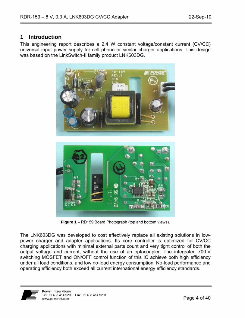
1 Introduction This engineering report describes a 2.4 W constant voltage/constant current (CV/CC) universal input power supply for cell phone or similar charger applications. This design was based on the LinkSwitch-II family product LNK603DG.
Figure 1 – RD159 Board Photograph (top and bottom views).
The LNK603DG was developed to cost effectively replace all existing solutions in low-power charger and adapter applications. Its core controller is optimized for CV/CC charging applications with minimal external parts count and very tight control of both the output voltage and current, without the use of an optocoupler. The integrated 700 V switching MOSFET and ON/OFF control function of this IC achieve both high efficiency under all load conditions, and low no-load energy consumption. No-load performance and operating efficiency both exceed all current international energy efficiency standards.

22-Sep-10 RDR-159 – 8 V, 0.3 A, LNK603DG CV/CC Adapter
Page 5 of 40
Power Integrations Tel: +1 408 414 9200 Fax: +1 408 414 9201
www.powerint.com
The LNK603DG monolithically integrates a 700 V power MOSFET switch and controller. CV regulation is achieved using a unique ON/OFF control scheme, cable voltage-drop compensation, and tight regulation over a wide temperature range. The switching frequency is modulated to regulate the output current to provide a linear CC characteristic. The LNK603DG controller consists of an oscillator, feedback (sense and logic) circuitry, a 5.8 V regulator, BYPASS pin programming functions, over-temperature protection, frequency jittering, current-limit circuitry, leading-edge blanking, a frequency controller for CC regulation, and an ON/OFF state machine for CV control all on one IC. The LNK603DG also provides a sophisticated range of protection features, including auto-restart for control-loop component open circuit or short-circuit faults and output short-circuit conditions. Accurate hysteretic thermal shutdown ensures safe average PCB temperatures under all conditions. The IC package provides extended creepage distance between high and low voltage pins (both at the package and the PCB), which is required in very humid conditions to prevent arcing and to further improve reliability. The LNK603DG can be configured as either self-biased from the high-voltage drain pin or supplied via an optional bias supply. When configured as self-biased, the very low IC current consumption provides a worst-case no-load power consumption of less than 50 mW at 265 VAC, well within the 300 mW European Union CoC limit. The EE16 transformer bobbin provides extended creepage to meet safety spacing requirements. To meet the 10 kV common-mode surge requirements, the transformer’s secondary leads are terminated directly to the PCB (flying leads). This document contains the power supply specifications, schematic, bill of materials, transformer specifications, and typical performance characteristics for this reference design.
RDR-159 – 8 V, 0.3 A, LNK603DG CV/CC Adapter 22-Sep-10
Page 6 of 40
Power Integrations Tel: +1 408 414 9200 Fax: +1 408 414 9201 www.powerint.com
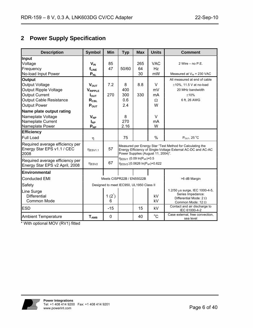
2 Power Supply Specification
Description Symbol Min Typ Max Units Comment
Input Voltage VIN 85 265 VAC 2 Wire – no P.E.
Frequency fLINE 47 50/60 64 Hz
No-load Input Power PNL 30 mW Measured at VIN = 230 VAC
Output All measured at end of cable
Output Voltage VOUT 7.2 8 8.8 V 10%, 11.5 V at no-load
Output Ripple Voltage VRIPPLE 400 mV 20 MHz bandwidth
Output Current IOUT 270 300 330 mA 10%
Output Cable Resistance RCBL 0.6 6 ft, 26 AWG
Output Power POUT 2.4 W
Name plate output rating
Nameplate Voltage VNP 8 V
Nameplate Current INP 270 mA
Nameplate Power PNP 2.16 W
Efficiency
Full Load 75 % POUT, 25 oC
Required average efficiency per Energy Star EPS v1.1 / CEC 2008
ESV1.1 57
Required average efficiency per Energy Star EPS v2 April, 2008 ESV2 67
Measured per Energy Star “Test Method for Calculating the Energy Efficiency of Single-Voltage External AC-DC and AC-AC Power Supplies (August 11, 2004)”.
ESV1 (0.09 ln(PNP)+0.5
ESV2:(0.0626 ln(PNP)+0.622
Environmental
Conducted EMI Meets CISPR22B / EN55022B >6 dB Margin
Safety Designed to meet IEC950, UL1950 Class II
Line Surge Differential Common Mode
1 (2*) 6
kV kV
1.2/50 s surge, IEC 1000-4-5, Series Impedance:
Differential Mode: 2 Common Mode: 12
ESD -15 15 kV Contact and air discharge to IEC 61000-4-2
Ambient Temperature TAMB 0 40 oC Case external, free convection, sea level
* With optional MOV (RV1) fitted
22-Sep-10 RDR-159 – 8 V, 0.3 A, LNK603DG CV/CC Adapter
Page 7 of 40
Power Integrations Tel: +1 408 414 9200 Fax: +1 408 414 9201
www.powerint.com
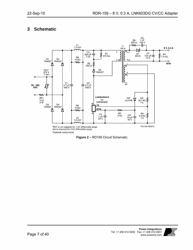
3 Schematic
Figure 2 – RD159 Circuit Schematic.
RDR-159 – 8 V, 0.3 A, LNK603DG CV/CC Adapter 22-Sep-10
Page 8 of 40
Power Integrations Tel: +1 408 414 9200 Fax: +1 408 414 9201 www.powerint.com
4 Circuit Description This circuit uses the LNK603DG in a primary-side regulated flyback power supply configuration.
4.1 Input Filter The AC input power is rectified by diodes D1 through D4. The rectified AC is filtered by bulk storage capacitors C1 and C2. Inductors L1 and L2, with capacitors C1 and C2, form pi (π) filters to attenuate conducted differential-mode EMI noise. This configuration, along with Power Integrations’ transformer E-shield technology, allows this design to meet EMI standard EN55022 class B with good margin and without a Y capacitor. In addition, the transformer’s construction gives very good EMI repeatability. Fusible resistor RF1 provides protection against catastrophic failure. It must be rated to withstand the instantaneous dissipation when the supply is first connected to the AC input (while the input capacitors charge) at VACMAX. This means choosing either an over-sized metal-film or a wire-wound resistor for RF1. Because of the dissipation levels, this design uses a wire-wound resistor (rather than a metal-film type). Note that RV1 is shown in the schematic, but it is not loaded on the PCB in this design since it is not necessary for withstanding a 1 kV differential surge. However, if your product is tested against, or expected to withstand, a 2 kV differential surge, load RV1 on the PCB.
4.2 LNK603DG Primary The LNK603DG (U1) incorporates a power switching MOSFET, an oscillator, a CV/CC control engine, and startup and protection functions on one IC. IC U1’s integrated 700 V MOSFET enables it to provide sufficient voltage margins for universal AC input applications, even in the event of extended line surges or swells. This is ideal in situations where AC voltage variations go beyond the standard universal AC input voltage range. To further simplify the power supply’s design, power U1 solely from the BYPASS pin via the decoupling capacitor C4. The optional bias supply (consisting of D6, C5, and R5) used in this design further reduces no-load input power, and increases efficiency with light loads. The rectified and filtered input voltage is applied to one side of transformer T1’s primary winding. The MOSFET drives the other side of the primary winding. The leakage inductance drain voltage spike is limited by an RCD-R clamp consisting of D5, R1, R2, and C3. Resistor R2 has a relatively large value to prevent any excessive ringing on the drain voltage waveform caused by the leakage inductance. Excessive ringing can increase output ripple by introducing an error in the sampled output voltage. IC U1 samples the feedback winding each cycle, 2.5 µs after turn-off of its internal MOSFET.
22-Sep-10 RDR-159 – 8 V, 0.3 A, LNK603DG CV/CC Adapter
Page 9 of 40
Power Integrations Tel: +1 408 414 9200 Fax: +1 408 414 9201
www.powerint.com
4.3 Output Rectification and Filtering The transformer’s secondary is rectified by D7, a Schottky-barrier diode, and filtered by C7. In this application, C7, having a low ESR value, meets the output voltage ripple requirement without an LC post filter. If it provides lower cost overall, select a smaller value for C7, and follow it with a ferrite bead and another capacitor (100 µF) to filter switching noise. In designs where lower (by 2% to 3%) average efficiency is acceptable, replace D7 with a PN-junction diode (such as an ES1A or UF4001) to lower cost. Adjust R3 and R4 accordingly, to keep the output voltage properly centered. Resistor R6 and capacitor C6 together dampen high-frequency ringing (therefore reducing radiated EMI) and reduce voltage spikes that may appear across D7.
4.4 Output Regulation The LNK603DG regulates the output using ON/OFF control for constant voltage (CV) regulation and frequency control for constant current (CC) regulation. The output voltage is sensed by the bias winding on T1. Feedback resistors R3 and R4 were selected using standard 1% resistor values to center both the nominal output voltage and the constant current regulation thresholds. Resistor R7 provides a minimum load to maintain output regulation when the output is unloaded.
RDR-159 – 8 V, 0.3 A, LNK603DG CV/CC Adapter 22-Sep-10
Page 10 of 40
Power Integrations Tel: +1 408 414 9200 Fax: +1 408 414 9201 www.powerint.com
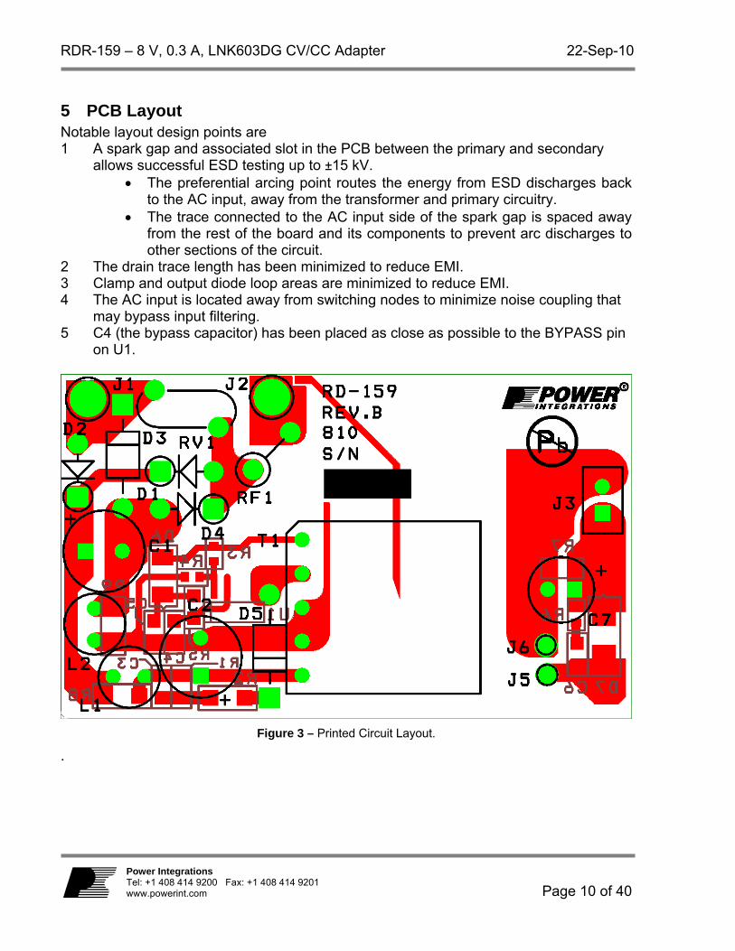
5 PCB Layout Notable layout design points are 1 A spark gap and associated slot in the PCB between the primary and secondary
allows successful ESD testing up to ±15 kV. The preferential arcing point routes the energy from ESD discharges back
to the AC input, away from the transformer and primary circuitry. The trace connected to the AC input side of the spark gap is spaced away
from the rest of the board and its components to prevent arc discharges to other sections of the circuit.
2 The drain trace length has been minimized to reduce EMI. 3 Clamp and output diode loop areas are minimized to reduce EMI. 4 The AC input is located away from switching nodes to minimize noise coupling that
may bypass input filtering. 5 C4 (the bypass capacitor) has been placed as close as possible to the BYPASS pin
on U1.
Figure 3 – Printed Circuit Layout.
.
22-Sep-10 RDR-159 – 8 V, 0.3 A, LNK603DG CV/CC Adapter
Page 11 of 40
Power Integrations Tel: +1 408 414 9200 Fax: +1 408 414 9201
www.powerint.com
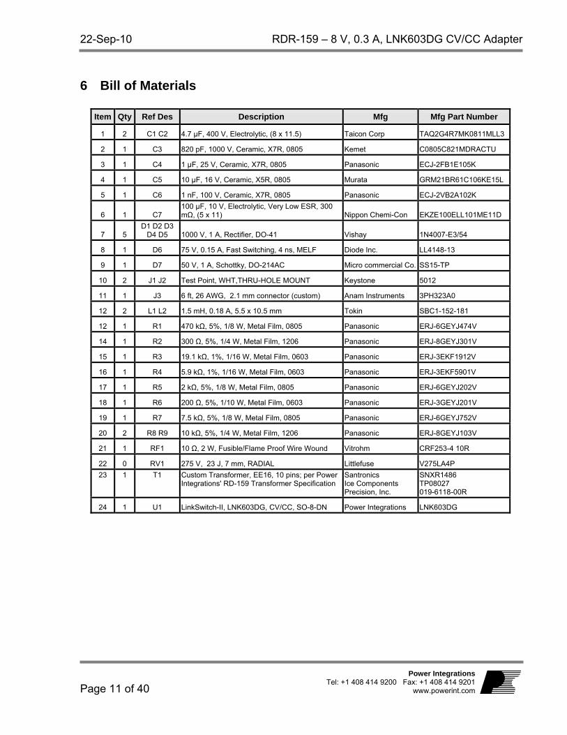
6 Bill of Materials
Item Qty Ref Des Description Mfg Mfg Part Number
1 2 C1 C2 4.7 μF, 400 V, Electrolytic, (8 x 11.5) Taicon Corp TAQ2G4R7MK0811MLL3
2 1 C3 820 pF, 1000 V, Ceramic, X7R, 0805 Kemet C0805C821MDRACTU
3 1 C4 1 μF, 25 V, Ceramic, X7R, 0805 Panasonic ECJ-2FB1E105K
4 1 C5 10 μF, 16 V, Ceramic, X5R, 0805 Murata GRM21BR61C106KE15L
5 1 C6 1 nF, 100 V, Ceramic, X7R, 0805 Panasonic ECJ-2VB2A102K
6 1 C7 100 μF, 10 V, Electrolytic, Very Low ESR, 300 mΩ, (5 x 11) Nippon Chemi-Con EKZE100ELL101ME11D
7 5 D1 D2 D3
D4 D5 1000 V, 1 A, Rectifier, DO-41 Vishay 1N4007-E3/54
8 1 D6 75 V, 0.15 A, Fast Switching, 4 ns, MELF Diode Inc. LL4148-13
9 1 D7 50 V, 1 A, Schottky, DO-214AC Micro commercial Co. SS15-TP
10 2 J1 J2 Test Point, WHT,THRU-HOLE MOUNT Keystone 5012
11 1 J3 6 ft, 26 AWG, 2.1 mm connector (custom) Anam Instruments 3PH323A0
12 2 L1 L2 1.5 mH, 0.18 A, 5.5 x 10.5 mm Tokin SBC1-152-181
12 1 R1 470 kΩ, 5%, 1/8 W, Metal Film, 0805 Panasonic ERJ-6GEYJ474V
14 1 R2 300 Ω, 5%, 1/4 W, Metal Film, 1206 Panasonic ERJ-8GEYJ301V
15 1 R3 19.1 kΩ, 1%, 1/16 W, Metal Film, 0603 Panasonic ERJ-3EKF1912V
16 1 R4 5.9 kΩ, 1%, 1/16 W, Metal Film, 0603 Panasonic ERJ-3EKF5901V
17 1 R5 2 kΩ, 5%, 1/8 W, Metal Film, 0805 Panasonic ERJ-6GEYJ202V
18 1 R6 200 Ω, 5%, 1/10 W, Metal Film, 0603 Panasonic ERJ-3GEYJ201V
19 1 R7 7.5 kΩ, 5%, 1/8 W, Metal Film, 0805 Panasonic ERJ-6GEYJ752V
20 2 R8 R9 10 kΩ, 5%, 1/4 W, Metal Film, 1206 Panasonic ERJ-8GEYJ103V
21 1 RF1 10 Ω, 2 W, Fusible/Flame Proof Wire Wound Vitrohm CRF253-4 10R
22 0 RV1 275 V, 23 J, 7 mm, RADIAL Littlefuse V275LA4P
23 1 T1 Custom Transformer, EE16, 10 pins; per Power Integrations' RD-159 Transformer Specification
Santronics Ice Components Precision, Inc.
SNXR1486 TP08027 019-6118-00R
24 1 U1 LinkSwitch-II, LNK603DG, CV/CC, SO-8-DN Power Integrations LNK603DG

RDR-159 – 8 V, 0.3 A, LNK603DG CV/CC Adapter 22-Sep-10
Page 12 of 40
Power Integrations Tel: +1 408 414 9200 Fax: +1 408 414 9201 www.powerint.com
7 Transformer Specification
7.1 Electrical Diagram
1
WD1 = Shield
WD2 = Primary WD4 = Secondary
3
2
5
NC
FL1
FL2
108T 35AWG
12T 2x30AWG
10T 24AWG
WD3 = Bias
9T 3x31AWG
4
Figure 4 – Transformer Electrical Diagram.
7.2 Electrical Specifications
Electrical Strength 60 second, 60 Hz, from pins 1-5 to pins 6-10 3000 VAC
Primary Inductance Pins 2-5, all other windings open, measured at 100 KHz, 0.4VRMS
2.28 mH, ±10%
Resonant Frequency Pins 2-5, all other windings open 800 kHz (min) Primary Leakage Inductance
Pins 3-5, with flying leads 1 and 2 shorted, measured at 100 kHz, 0.4 VRMS 65 H (max)
7.3 Materials
Item Description
[1] Core: EE16, NC-2H or equivalent, gapped for ALG of 143 nH/T2
[2] Bobbin: EE16, Horizontal, 10 pins, (5/5)
[3] Magnet Wire: #30 AWG
[4] Magnet Wire: #31 AWG
[5] Magnet Wire: #35 AWG
[6] Triple Insulated Wire: #24 AWG
[7] Margin tape: 1.0 mm wide
[8] Tape: 3M 1298 Polyester film, 2.0 mils thick, 8.0 mm wide
[9] Tape: 3M Polyester film, 2.0 mils thick, 7.0 mm wide
[10] Varnish
22-Sep-10 RDR-159 – 8 V, 0.3 A, LNK603DG CV/CC Adapter
Page 13 of 40
Power Integrations Tel: +1 408 414 9200 Fax: +1 408 414 9201
www.powerint.com
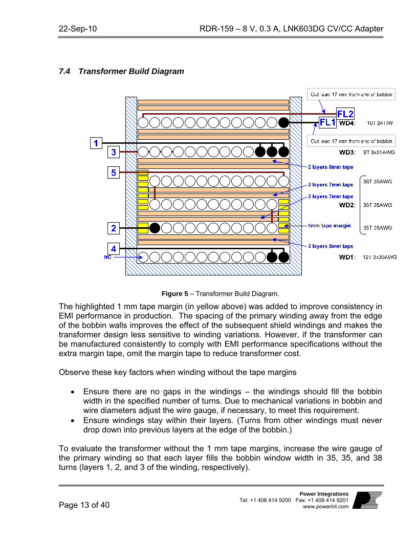
7.4 Transformer Build Diagram
Figure 5 – Transformer Build Diagram.
The highlighted 1 mm tape margin (in yellow above) was added to improve consistency in EMI performance in production. The spacing of the primary winding away from the edge of the bobbin walls improves the effect of the subsequent shield windings and makes the transformer design less sensitive to winding variations. However, if the transformer can be manufactured consistently to comply with EMI performance specifications without the extra margin tape, omit the margin tape to reduce transformer cost. Observe these key factors when winding without the tape margins
Ensure there are no gaps in the windings – the windings should fill the bobbin width in the specified number of turns. Due to mechanical variations in bobbin and wire diameters adjust the wire gauge, if necessary, to meet this requirement.
Ensure windings stay within their layers. (Turns from other windings must never drop down into previous layers at the edge of the bobbin.)
To evaluate the transformer without the 1 mm tape margins, increase the wire gauge of the primary winding so that each layer fills the bobbin window width in 35, 35, and 38 turns (layers 1, 2, and 3 of the winding, respectively).
RDR-159 – 8 V, 0.3 A, LNK603DG CV/CC Adapter 22-Sep-10
Page 14 of 40
Power Integrations Tel: +1 408 414 9200 Fax: +1 408 414 9201 www.powerint.com
7.5 Transformer Construction
Bobbin Preparation
Primary side of the bobbin is placed on the left-hand side, and secondary side of the bobbin is placed on the right-hand side.
WD1 Shield
Temporarily hanging the start end of the wires of item [3] on pin 6, evenly wind 12 bi-filar turns from right to left with tight tension. The maximum allowed gap between the winding and the left and right lateral walls of the bobbin must be less than 0.5 mm (20 mils). Cut the end of the wire to leave it NC (no connection), and bring the start end of the wire across the bobbin to the left to terminate at pin 4.
Insulation 2 layers of tape item [8].
WD2 Primary
Apply 1 mm margin tape item [7] on both sides of bobbin to match the height of first layer of primary winding (approximately 2 turns) on the left side, and first two layers on the right side (approximately 4 turns). Start at pin 2, wind 35 turns of item [5] from left to right with tight tension and apply 2 layers tape item [9]. On the left side, apply 1mm margin tape [7] to match another two layers. Continue winding 35 turns of item [5] from right to left. Apply 2 layer tape item [9], continue wind 38 turns of item [5] from left to right, and at the last turn bring the wire back to the left to terminate at pin 5.
Insulation 2 layers of tape item [8].
WD3 Bias
Temporarily hang the start end of the wires of item [4] on pin 8, wind 9 tri-filar turns from right to left uniformly, terminate the end of the wires at pin 3, bring the start end of the wires across the bobbin to the left side to terminate at pin 1.
Insulation 2 layers of tape item [8].
WD4 Secondary
Temporarily hang the start end of the wire of item [6] on pin 6 and leave it about 17 mm long, wind 10 turns of item [6] from right to left uniformly. At the last turn bring the wire across the bobbin to the right side. Leave this end floating, about 17 mm long.
Insulation 2 layers of tape item [8].
Finish Remove all pins on the secondary side. Gap the core to meet required primary inductance value. Secure the core with tape. Dip vanish [10].
Note: Tape between adjacent primary winding layers reduces primary capacitance and losses, improving no-load input power and light-load efficiency.

22-Sep-10 RDR-159 – 8 V, 0.3 A, LNK603DG CV/CC Adapter
Page 15 of 40
Power Integrations Tel: +1 408 414 9200 Fax: +1 408 414 9201
www.powerint.com
Design Spreadsheet
RD-159 Power Integrations INPUT OUTPUT UNIT
ACDC_LinkSwitch-II_040108_Rev1-0.xls; LinkSwitch-II Discontinuous Flyback
Transformer Design Spreadsheet ENTER APPLICATION VARIABLES
VACMIN 85 V Minimum AC Input Voltage
VACMAX 265 V Maximum AC Input Voltage fL 50 Hz AC Mains Frequency VO 8 V Output Voltage (at continuous power) IO 0.3 A Power Supply Output Current
(corresponding to peak power) Power 2.40 W Continuous Output Power n 0.70 Efficiency Estimate at output terminals.
Under 0.7 if no better data available
Z 0.50 Z Factor. Ratio of secondary side losses to the total losses in the power supply. Use 0.5 if no better data available
tC 3.00 ms Bridge Rectifier Conduction Time Estimate Add Bias Winding YES YES Choose Yes to add a Bias winding to power
the LinkSwitch-II. CIN 9.4 uF Input Capacitance
ENTER LinkSwitch-II VARIABLES
Chosen Device LNK603 LNK603 Chosen LinkSwitch-II device Package DG DG Select package (PG, GG or DG)
ILIMITMIN 0.19 A Minimum Current Limit ILIMITTYP 0.20 A Typical Current Limit ILIMITMAX 0.22 A Maximum Current Limit FS 64 64.00 kHz Typical Device Switching Frequency at
maximum power VOR 90.72 V Reflected Output Voltage (VOR < 135 V
Recommended)
VDS 10.00 V LinkSwitch-II on-state Drain to Source Voltage
VD 0.4 0.40 V Output Winding Diode Forward Voltage Drop
KP 2.70 Ensure KDP > 1.3 for discontinuous mode operation
FEEDBACK WINDING PARAMETERS
NFB 9.00 Feedback winding turns VFLY 7.56 V Flyback Voltage VFOR 8.06 V Forward voltage

RDR-159 – 8 V, 0.3 A, LNK603DG CV/CC Adapter 22-Sep-10
Page 16 of 40
Power Integrations Tel: +1 408 414 9200 Fax: +1 408 414 9201 www.powerint.com
BIAS WINDING PARAMETERS
VB 7.2 7.20 V Bias Winding Voltage. Ensure that VB > VFLY. Bias winding is assumed to be AC-STACKED on top of Feedback winding
NB 0.00 Bias Winding number of turns
DESIGN PARAMETERS
DCON 4.5 4.50 us Output diode conduction time TON 4.03 us LinkSwitch-II On-time (calculated at
minimum inductance) RUPPER 18.02 k-ohm Upper resistor in Feedback resistor divider RLOWER 5.96 k-ohm Lower resistor in resistor divider
ENTER TRANSFORMER CORE/CONSTRUCTION VARIABLES
Core Type Core EE16 EE16 Enter Transformer Core. Based on the
output power the recommended core sizes are EE13 or EE16
Bobbin EE16_BOBBIN Generic EE16_BOBBIN AE 19.20 mm^2 Core Effective Cross Sectional Area LE 35.00 mm^2 Core Effective Path Length AL 1140.00 nH/tur
n^2 Ungapped Core Effective Inductance
BW 8.60 mm Bobbin Physical Winding Width M 1 1.00 mm Safety Margin Width (Half the Primary to
Secondary Creepage Distance) L 3.00 Number of Primary Layers NS 10.00 Number of Secondary Turns. To adjust
Secondary number of turns change DCON
DC INPUT VOLTAGE PARAMETERS
VMIN 96.66 V Minimum DC bus voltage VMAX 374.77 V Maximum DC bus voltage
CURRENT WAVEFORM SHAPE PARAMETERS
DMAX 0.26 Maximum duty cycle measured at VMIN IAVG 0.04 A Input Average current IP 0.19 A Peak primary current IR 0.19 A primary ripple current IRMS 0.06 A Primary RMS current
22-Sep-10 RDR-159 – 8 V, 0.3 A, LNK603DG CV/CC Adapter
Page 17 of 40
Power Integrations Tel: +1 408 414 9200 Fax: +1 408 414 9201
www.powerint.com
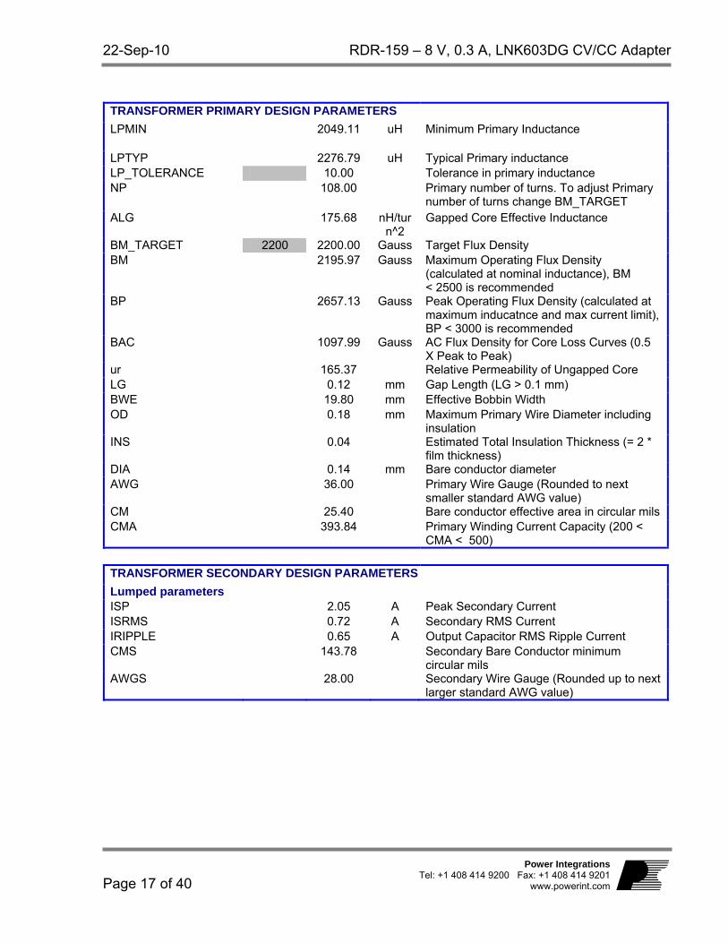
TRANSFORMER PRIMARY DESIGN PARAMETERS
LPMIN 2049.11 uH Minimum Primary Inductance
LPTYP 2276.79 uH Typical Primary inductance LP_TOLERANCE 10.00 Tolerance in primary inductance NP 108.00 Primary number of turns. To adjust Primary
number of turns change BM_TARGET ALG 175.68 nH/tur
n^2 Gapped Core Effective Inductance
BM_TARGET 2200 2200.00 Gauss Target Flux Density BM 2195.97 Gauss Maximum Operating Flux Density
(calculated at nominal inductance), BM < 2500 is recommended
BP 2657.13 Gauss Peak Operating Flux Density (calculated at maximum inducatnce and max current limit), BP < 3000 is recommended
BAC 1097.99 Gauss AC Flux Density for Core Loss Curves (0.5 X Peak to Peak)
ur 165.37 Relative Permeability of Ungapped Core LG 0.12 mm Gap Length (LG > 0.1 mm) BWE 19.80 mm Effective Bobbin Width OD 0.18 mm Maximum Primary Wire Diameter including
insulation INS 0.04 Estimated Total Insulation Thickness (= 2 *
film thickness) DIA 0.14 mm Bare conductor diameter AWG 36.00 Primary Wire Gauge (Rounded to next
smaller standard AWG value) CM 25.40 Bare conductor effective area in circular mils CMA 393.84 Primary Winding Current Capacity (200 <
CMA < 500)
TRANSFORMER SECONDARY DESIGN PARAMETERS
Lumped parameters ISP 2.05 A Peak Secondary Current ISRMS 0.72 A Secondary RMS Current IRIPPLE 0.65 A Output Capacitor RMS Ripple Current CMS 143.78 Secondary Bare Conductor minimum
circular mils AWGS 28.00 Secondary Wire Gauge (Rounded up to next
larger standard AWG value)
RDR-159 – 8 V, 0.3 A, LNK603DG CV/CC Adapter 22-Sep-10
Page 18 of 40
Power Integrations Tel: +1 408 414 9200 Fax: +1 408 414 9201 www.powerint.com
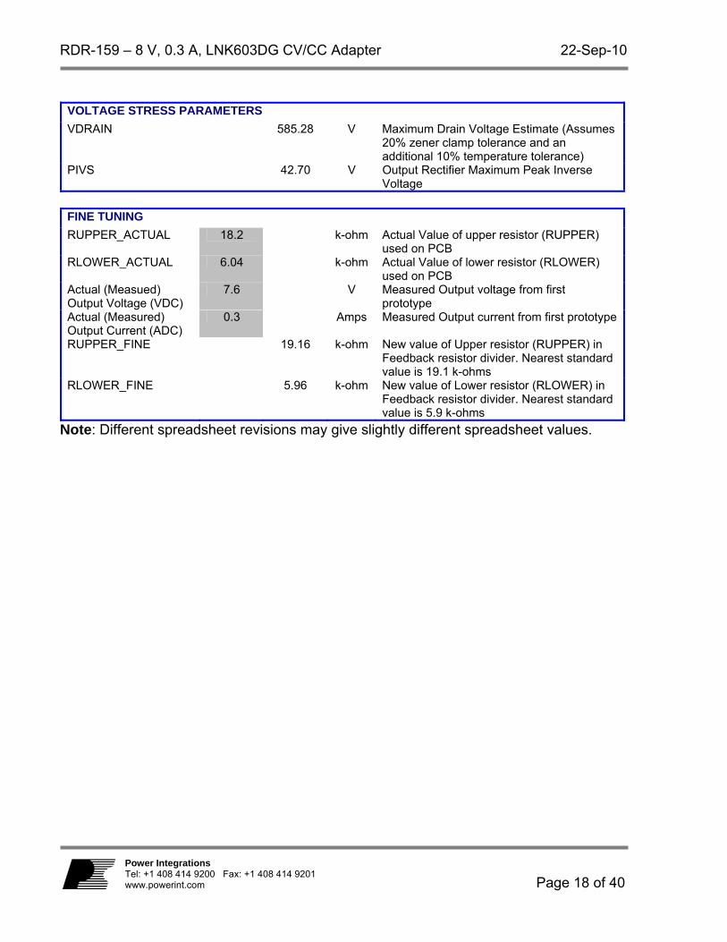
VOLTAGE STRESS PARAMETERS
VDRAIN 585.28 V Maximum Drain Voltage Estimate (Assumes 20% zener clamp tolerance and an additional 10% temperature tolerance)
PIVS 42.70 V Output Rectifier Maximum Peak Inverse Voltage
FINE TUNING
RUPPER_ACTUAL 18.2 k-ohm Actual Value of upper resistor (RUPPER) used on PCB
RLOWER_ACTUAL 6.04 k-ohm Actual Value of lower resistor (RLOWER) used on PCB
Actual (Measued) Output Voltage (VDC)
7.6 V Measured Output voltage from first prototype
Actual (Measured) Output Current (ADC)
0.3 Amps Measured Output current from first prototype
RUPPER_FINE 19.16 k-ohm New value of Upper resistor (RUPPER) in Feedback resistor divider. Nearest standard value is 19.1 k-ohms
RLOWER_FINE 5.96 k-ohm New value of Lower resistor (RLOWER) in Feedback resistor divider. Nearest standard value is 5.9 k-ohms
Note: Different spreadsheet revisions may give slightly different spreadsheet values.

22-Sep-10 RDR-159 – 8 V, 0.3 A, LNK603DG CV/CC Adapter
Page 19 of 40
Power Integrations Tel: +1 408 414 9200 Fax: +1 408 414 9201
www.powerint.com
Performance Data All measurements were taken at room temperature unless otherwise specified, with a 60 Hz input frequency, and at the end of a 6 ft, 0.5 Ώ, 26 AWG output cable.
7.6 Efficiency
50%
55%
60%
65%
70%
75%
80%
85%
90%
0 0.5 1 1.5 2 2.5
Output Power (W)
Eff
icie
ncy
(%
)
Vin = 85 VAC
Vin = 115 VAC
Vin = 230 VAC
Vin = 265 VAC
Figure 6 – Efficiency vs. Output Power.
RDR-159 – 8 V, 0.3 A, LNK603DG CV/CC Adapter 22-Sep-10
Page 20 of 40
Power Integrations Tel: +1 408 414 9200 Fax: +1 408 414 9201 www.powerint.com
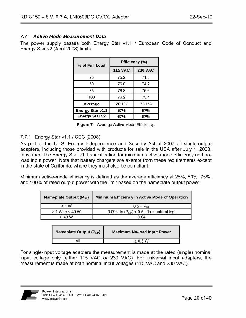
7.7 Active Mode Measurement Data The power supply passes both Energy Star v1.1 / European Code of Conduct and Energy Star v2 (April 2008) limits.
Efficiency (%) % of Full Load
115 VAC 230 VAC
25 75.2 71.5
50 76.0 74.2
75 76.8 75.6
100 76.2 75.4
Average 76.1% 75.1%
Energy Star v1.1 57% 57%
Energy Star v2 67% 67%
Figure 7 – Average Active Mode Efficiency.
7.7.1 Energy Star v1.1 / CEC (2008)
As part of the U. S. Energy Independence and Security Act of 2007 all single-output adapters, including those provided with products for sale in the USA after July 1, 2008, must meet the Energy Star v1.1 specification for minimum active-mode efficiency and no-load input power. Note that battery chargers are exempt from these requirements except in the state of California, where they must also be compliant. Minimum active-mode efficiency is defined as the average efficiency at 25%, 50%, 75%, and 100% of rated output power with the limit based on the nameplate output power:
Nameplate Output (PNP) Minimum Efficiency in Active Mode of Operation
< 1 W 0.5 PNP 1 W to 49 W 0.09 ln (PNP) + 0.5 [ln = natural log]
> 49 W 0.84
Nameplate Output (PNP) Maximum No-load Input Power
All 0.5 W
For single-input voltage adapters the measurement is made at the rated (single) nominal input voltage only (either 115 VAC or 230 VAC). For universal input adapters, the measurement is made at both nominal input voltages (115 VAC and 230 VAC).
22-Sep-10 RDR-159 – 8 V, 0.3 A, LNK603DG CV/CC Adapter
Page 21 of 40
Power Integrations Tel: +1 408 414 9200 Fax: +1 408 414 9201
www.powerint.com
To meet the standard, the measured average efficiency (or efficiencies for universal input supplies) must be greater than or equal to the efficiency specified by the CEC/Energy Star v1.1 standard.

RDR-159 – 8 V, 0.3 A, LNK603DG CV/CC Adapter 22-Sep-10
Page 22 of 40
Power Integrations Tel: +1 408 414 9200 Fax: +1 408 414 9201 www.powerint.com
7.7.2 Energy Star v2 (April 2008)
The Energy Star v2 specification (planned to take effect Nov 1, 2008) increases the previously stated requirements. Standard Models
Nameplate Output (PNP) Minimum Efficiency in Active Mode of Operation
(Rounded to Hundreds)
1 W 0.48 PNP + 0.14
> 1 W to 49 W 0.0626 ln (PNP) + 0.622 [ln = natural log]
> 49 W 0.87
Nameplate Output (PNP) Maximum No-load Input Power
0 to <50 W 0.3 W 50 to 250 W 0.5 W
Low-voltage Models A low-voltage model is an external power supply (EPS) with a nameplate output voltage of less than 6 V and a nameplate output current greater than or equal to 550 mA.
Nameplate Output (PNP) Minimum Efficiency in Active Mode of Operation
(Rounded to Hundreds)
1 W 0.497 PNP + 0.067
>1 W to 49 W 0.075 ln (PNP) + 0.561
[ln = natural log] >49 W 0.86
Nameplate Output (PNP) Maximum No-load Input Power
0 to <50 W 0.3 W 50 to 250 W 0.5 W
For the latest up-to-date information, please visit the PI Green Room at www.powerint.com.

22-Sep-10 RDR-159 – 8 V, 0.3 A, LNK603DG CV/CC Adapter
Page 23 of 40
Power Integrations Tel: +1 408 414 9200 Fax: +1 408 414 9201
www.powerint.com
7.8 No-Load Input Power
15
20
25
30
35
40
45
50
80 100 120 140 160 180 200 220 240 260 280
Input Voltage (VAC)
No
Lo
ad
Inp
ut
Po
we
r (m
W)
Figure 8 – Typical Zero Load Input Power vs. Input Line Voltage, Room Temperature, 60 Hz.
RDR-159 – 8 V, 0.3 A, LNK603DG CV/CC Adapter 22-Sep-10
Page 24 of 40
Power Integrations Tel: +1 408 414 9200 Fax: +1 408 414 9201 www.powerint.com
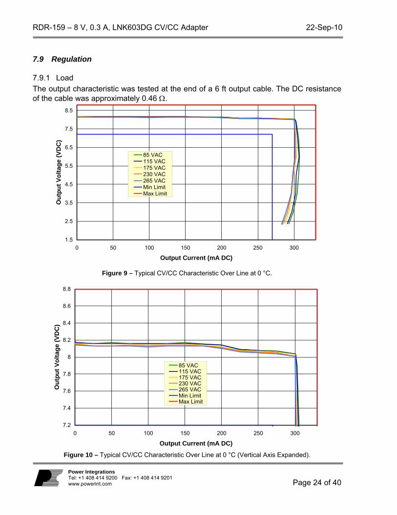
7.9 Regulation
7.9.1 Load
The output characteristic was tested at the end of a 6 ft output cable. The DC resistance of the cable was approximately 0.46 .
1.5
2.5
3.5
4.5
5.5
6.5
7.5
8.5
0 50 100 150 200 250 300
Output Current (mA DC)
Ou
tpu
t V
olt
age
(VD
C)
85 VAC115 VAC175 VAC230 VAC265 VACMin LimitMax Limit
Figure 9 – Typical CV/CC Characteristic Over Line at 0 °C.
7.2
7.4
7.6
7.8
8
8.2
8.4
8.6
8.8
0 50 100 150 200 250 300
Output Current (mA DC)
Ou
tpu
t V
olt
age
(VD
C)
85 VAC115 VAC175 VAC230 VAC265 VACMin LimitMax Limit
Figure 10 – Typical CV/CC Characteristic Over Line at 0 °C (Vertical Axis Expanded).

22-Sep-10 RDR-159 – 8 V, 0.3 A, LNK603DG CV/CC Adapter
Page 25 of 40
Power Integrations Tel: +1 408 414 9200 Fax: +1 408 414 9201
www.powerint.com
1.5
2.5
3.5
4.5
5.5
6.5
7.5
8.5
0 50 100 150 200 250 300
Output Current (mA DC)
Ou
tpu
t V
olt
age
(VD
C)
85 VAC115 VAC175 VAC230 VAC265 VACMin limitMax Limit
Figure 11 – Typical CV/CC Characteristic Over Line at 25 °C.
7.2
7.4
7.6
7.8
8
8.2
8.4
8.6
8.8
0 50 100 150 200 250 300
Output Current (mA DC)
Ou
tpu
t V
olt
age
(VD
C)
85 VAC115 VAC175 VAC230 VAC265 VACMin LimitMax Limit
Figure 12 – Typical CV/CC Characteristic Over Line at 25 °C (Vertical Axis Expanded).

RDR-159 – 8 V, 0.3 A, LNK603DG CV/CC Adapter 22-Sep-10
Page 26 of 40
Power Integrations Tel: +1 408 414 9200 Fax: +1 408 414 9201 www.powerint.com
1.5
2.5
3.5
4.5
5.5
6.5
7.5
8.5
0 50 100 150 200 250 300
Output Current (mA DC)
Ou
tpu
t V
olt
age
(VD
C)
85 VAC115 VAC175 VAC230 VAC265 VACMin limitMax Limit
Figure 13 – Typical CV/CC Characteristic Over Line at 40 °C.
7.2
7.4
7.6
7.8
8
8.2
8.4
8.6
8.8
0 50 100 150 200 250 300Output Current (mA DC)
Ou
tpu
t V
olt
age
(V
DC
)
85 VAC115 VAC175 VAC230 VAC265 VACMin limitMax Limit
Figure 14 – Typical CV/CC Characteristic Over Line at 40 °C (Vertical Axis Expanded).

22-Sep-10 RDR-159 – 8 V, 0.3 A, LNK603DG CV/CC Adapter
Page 27 of 40
Power Integrations Tel: +1 408 414 9200 Fax: +1 408 414 9201
www.powerint.com
8 Thermal Performance
8.1 Operating Temperature Survey Thermal performance was measured inside an enclosure with no airflow, and with the power supply driving a full load. A thermocouple was attached to U1 at its Source Pin.
Item 85 VAC 115 VAC 175 VAC 230 VAC 265 VAC
Ambient 40 °C 40 °C 40 °C 40 °C 40 °C
U1 Source Pin 67 °C 65 °C 66 °C 68 °C 70 °C
RDR-159 – 8 V, 0.3 A, LNK603DG CV/CC Adapter 22-Sep-10
Page 28 of 40
Power Integrations Tel: +1 408 414 9200 Fax: +1 408 414 9201 www.powerint.com
9 Waveforms
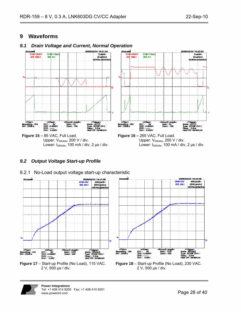
9.1 Drain Voltage and Current, Normal Operation
Figure 15 – 85 VAC, Full Load. Upper: VDRAIN, 200 V / div. Lower: IDRAIN, 100 mA / div, 2 µs / div.
Figure 16 – 265 VAC, Full Load. Upper: VDRAIN, 200 V / div. Lower: IDRAIN, 100 mA / div, 2 µs / div.
9.2 Output Voltage Start-up Profile
9.2.1 No-Load output voltage start-up characteristic
Figure 17 – Start-up Profile (No Load), 115 VAC. 2 V, 500 µs / div.
Figure 18 – Start-up Profile (No Load), 230 VAC. 2 V, 500 µs / div.

22-Sep-10 RDR-159 – 8 V, 0.3 A, LNK603DG CV/CC Adapter
Page 29 of 40
Power Integrations Tel: +1 408 414 9200 Fax: +1 408 414 9201
www.powerint.com
9.2.2 Output Voltage Start-up Characteristic with a Resistive Load (27 ) Voltage was measured at the load.
Figure 19 – Start-up Profile, 115 VAC. 2 V, 2 ms / div.
Figure 20 – Start-up Profile, 230 VAC. 2 V, 2 ms / div.
RDR-159 – 8 V, 0.3 A, LNK603DG CV/CC Adapter 22-Sep-10
Page 30 of 40
Power Integrations Tel: +1 408 414 9200 Fax: +1 408 414 9201 www.powerint.com
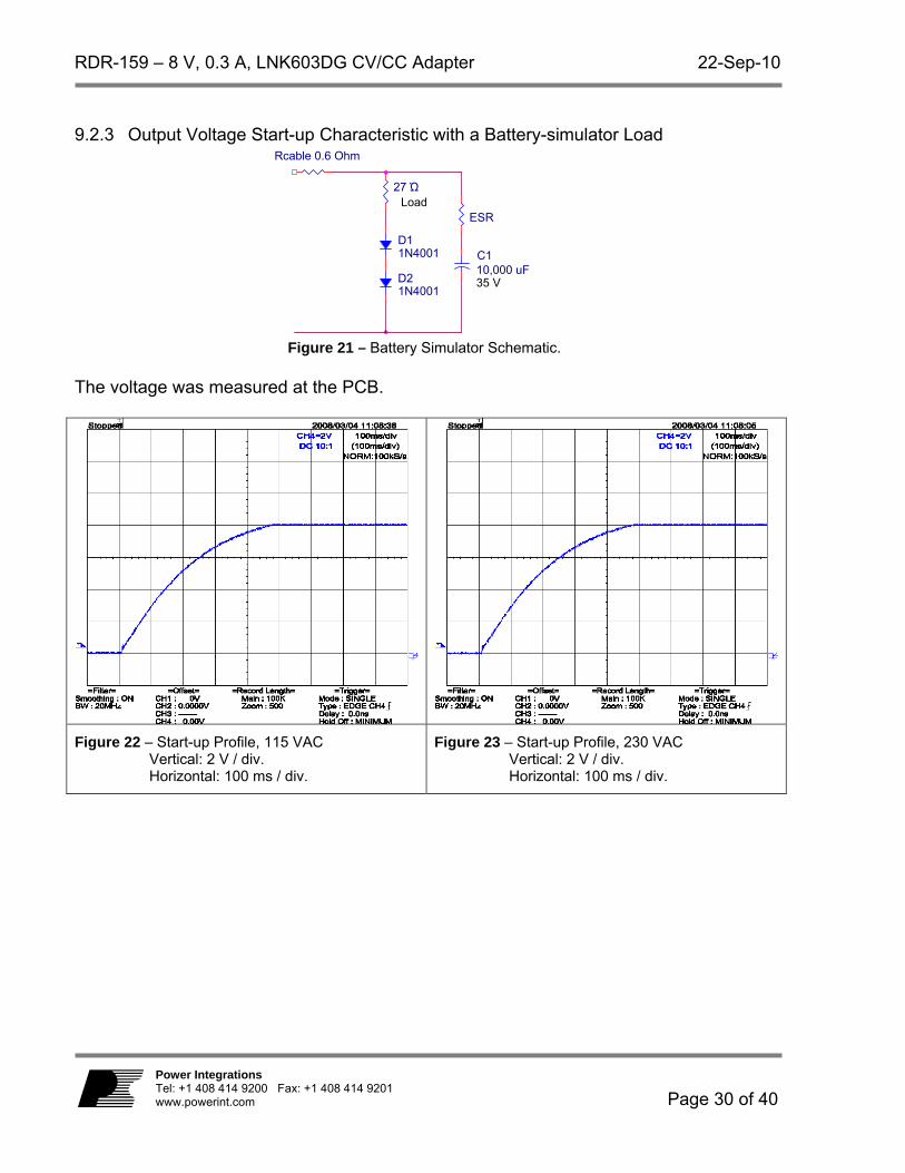
9.2.3 Output Voltage Start-up Characteristic with a Battery-simulator Load
Figure 21 – Battery Simulator Schematic.
The voltage was measured at the PCB.
Figure 22 – Start-up Profile, 115 VAC Vertical: 2 V / div. Horizontal: 100 ms / div.
Figure 23 – Start-up Profile, 230 VAC Vertical: 2 V / div. Horizontal: 100 ms / div.
C110,000 uF35 V
D11N4001
D21N4001
ESR
27 ΏLoad
Rcable 0.6 Ohm

22-Sep-10 RDR-159 – 8 V, 0.3 A, LNK603DG CV/CC Adapter
Page 31 of 40
Power Integrations Tel: +1 408 414 9200 Fax: +1 408 414 9201
www.powerint.com
9.3 Drain Voltage and Current Start-up Profile
Figure 24 – 85 VAC Input and Maximum Load
Upper: VDRAIN, 200 V, 2 ms / div. Lower: IDRAIN, 100 mA / div.
Figure 25 – 265 VAC Input and Maximum Load Upper: VDRAIN, 200 V, 2 ms / div. Lower: IDRAIN, 100 mA / div.
RDR-159 – 8 V, 0.3 A, LNK603DG CV/CC Adapter 22-Sep-10
Page 32 of 40
Power Integrations Tel: +1 408 414 9200 Fax: +1 408 414 9201 www.powerint.com
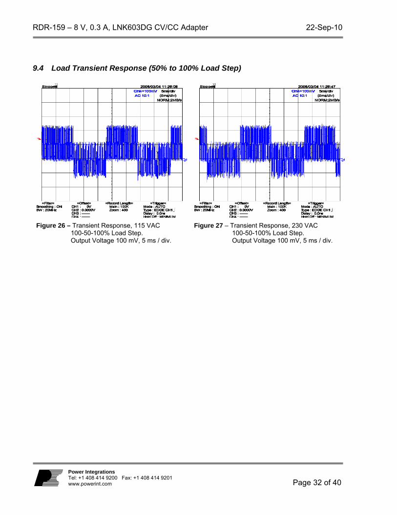
9.4 Load Transient Response (50% to 100% Load Step)
Figure 26 – Transient Response, 115 VAC 100-50-100% Load Step. Output Voltage 100 mV, 5 ms / div.
Figure 27 – Transient Response, 230 VAC 100-50-100% Load Step. Output Voltage 100 mV, 5 ms / div.
22-Sep-10 RDR-159 – 8 V, 0.3 A, LNK603DG CV/CC Adapter
Page 33 of 40
Power Integrations Tel: +1 408 414 9200 Fax: +1 408 414 9201
www.powerint.com
9.5 Output Ripple Measurements
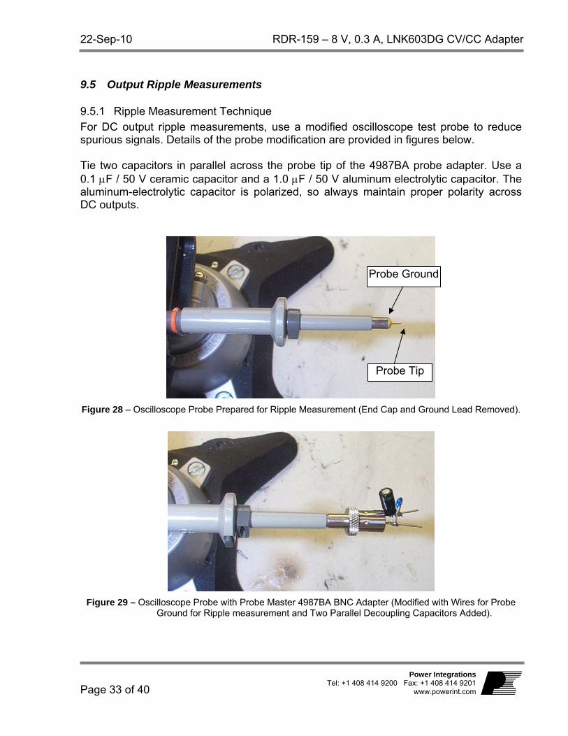
9.5.1 Ripple Measurement Technique
For DC output ripple measurements, use a modified oscilloscope test probe to reduce spurious signals. Details of the probe modification are provided in figures below. Tie two capacitors in parallel across the probe tip of the 4987BA probe adapter. Use a 0.1 F / 50 V ceramic capacitor and a 1.0 F / 50 V aluminum electrolytic capacitor. The aluminum-electrolytic capacitor is polarized, so always maintain proper polarity across DC outputs.
Figure 28 – Oscilloscope Probe Prepared for Ripple Measurement (End Cap and Ground Lead Removed).
Figure 29 – Oscilloscope Probe with Probe Master 4987BA BNC Adapter (Modified with Wires for Probe
Ground for Ripple measurement and Two Parallel Decoupling Capacitors Added).
Probe Ground
Probe Tip
RDR-159 – 8 V, 0.3 A, LNK603DG CV/CC Adapter 22-Sep-10
Page 34 of 40
Power Integrations Tel: +1 408 414 9200 Fax: +1 408 414 9201 www.powerint.com
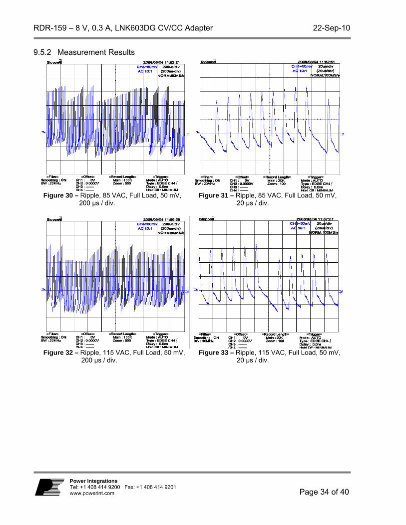
9.5.2 Measurement Results
Figure 30 – Ripple, 85 VAC, Full Load, 50 mV, 200 µs / div.
Figure 31 – Ripple, 85 VAC, Full Load, 50 mV, 20 μs / div.
Figure 32 – Ripple, 115 VAC, Full Load, 50 mV, 200 µs / div.
Figure 33 – Ripple, 115 VAC, Full Load, 50 mV, 20 μs / div.
22-Sep-10 RDR-159 – 8 V, 0.3 A, LNK603DG CV/CC Adapter
Page 35 of 40
Power Integrations Tel: +1 408 414 9200 Fax: +1 408 414 9201
www.powerint.com
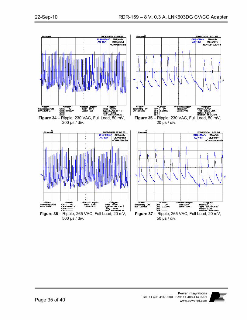
Figure 34 – Ripple, 230 VAC, Full Load, 50 mV, 200 µs / div.
Figure 35 – Ripple, 230 VAC, Full Load, 50 mV, 20 μs / div.
Figure 36 – Ripple, 265 VAC, Full Load, 20 mV, 500 µs / div.
Figure 37 – Ripple, 265 VAC, Full Load, 20 mV, 50 μs / div.

RDR-159 – 8 V, 0.3 A, LNK603DG CV/CC Adapter 22-Sep-10
Page 36 of 40
Power Integrations Tel: +1 408 414 9200 Fax: +1 408 414 9201 www.powerint.com
10 Line Surge Differential input line surge (1.2 µs / 50 µs) testing to specification IEC61000-4-5 was completed on a single test unit. The input voltage was 230 VAC, with a 60 Hz frequency. The supply was operated driving a full load. An additional LED connected to the load verified operation during, and following, each discharge.
Surge Level
(V)
Input Voltage (VAC)
Injection Location
Mode Injection
Phase (°)
Test Result (Pass/Fail)
+500 230 L to N 90 Pass -500 230 L to N 270 Pass +750 230 L to N 90 Pass -750 230 L to N 270 Pass
+1000 230 L to N 90 Pass -1000 230 L to N
Differential
270 Pass +6000 230 L+N to PE 90 Pass -6000 230 L+N to PE
Common 270 Pass
Adding MOV RV1 increases the differential mode ESD immunity to 2 kV.
11 ESD Both air and output contact ESD discharge testing was performed to IEC61000-4-2. In addition to the 10 events per polarity specified in this standard, free-running tests were also performed. More that 50 discharges were applied to the unit, with no failures. The input voltage was 265 VAC, with a 60 Hz frequency. The supply was operated driving a full load. An additional LED connected to the load verified operation during, and following, each discharge.
Surge Level (kV)
Input Voltage (VAC)
Injection Location
Events Test Result (Pass/Fail)
Output RTN +15
Output Output RTN -15
265
Output
10 + free running
Pass

22-Sep-10 RDR-159 – 8 V, 0.3 A, LNK603DG CV/CC Adapter
Page 37 of 40
Power Integrations Tel: +1 408 414 9200 Fax: +1 408 414 9201
www.powerint.com
12 Conducted EMI
Figure 38 – Conducted EMI 115 VAC Input, Neutral Measurement, Output Earth Grounded.
Figure 39 – 115 VAC Neutral, Table of Plot Shown on Left.
Figure 40 – Conducted EMI 115 VAC Input, Line Measurement, Output Earth Grounded.
Figure 41 – 115 VAC Line, Table of Plot Shown on Left.
RDR-159 – 8 V, 0.3 A, LNK603DG CV/CC Adapter 22-Sep-10
Page 38 of 40
Power Integrations Tel: +1 408 414 9200 Fax: +1 408 414 9201 www.powerint.com
Power Integrations
150 kHz 100 MHz
1 QPCLRWR
2 AVCLRWR
SGL
TDF
6DB
dBµV dBµV
RBW 9 kHz
MT 500 ms
Att 10 dB AUTO
29.Jan 08 11:11
1 MHz 10 MHz 100 MHz
-20
-10
0
10
20
30
40
50
60
70
80
LIMIT CHECK PASS
1
Marker 1 [T1 ]
43.60 dBµV
673.936068749 kHz
EN55022A
EN55022Q
MEI LNK363; 30VAC with hand
Date: 29.JAN.2008 11:11:11
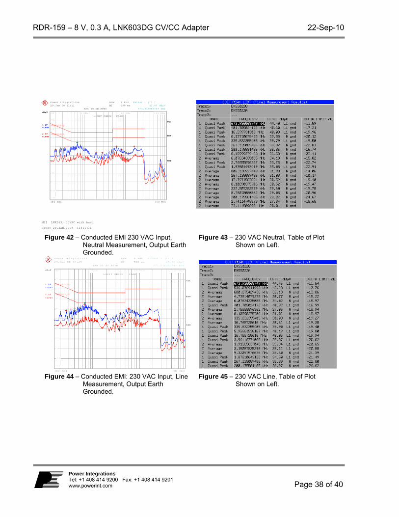
Figure 42 – Conducted EMI 230 VAC Input, Neutral Measurement, Output Earth Grounded.
Figure 43 – 230 VAC Neutral, Table of Plot Shown on Left.
Figure 44 – Conducted EMI: 230 VAC Input, Line Measurement, Output Earth Grounded.
Figure 45 – 230 VAC Line, Table of Plot Shown on Left.

22-Sep-10 RDR-159 – 8 V, 0.3 A, LNK603DG CV/CC Adapter
Page 39 of 40
Power Integrations Tel: +1 408 414 9200 Fax: +1 408 414 9201
www.powerint.com
13 Revision History
Date Author Revision Description and changes Reviewed 15-May-08 JC 1.0 Initial release JD 02-Oct-08 PV 1.1 Updated Section 2 - Common
Mode Line Surge from 2 to 6kV
22-Sep-10 KM 1.2 Updated schematic
RDR-159 – 8 V, 0.3 A, LNK603DG CV/CC Adapter 22-Sep-10
Page 40 of 40
Power Integrations Tel: +1 408 414 9200 Fax: +1 408 414 9201 www.powerint.com
For the latest updates, visit our website: www.powerint.com Power Integrations reserves the right to make changes to its products at any time to improve reliability or manufacturability. Power Integrations does not assume any liability arising from the use of any device or circuit described herein. POWER INTEGRATIONS MAKES NO WARRANTY HEREIN AND SPECIFICALLY DISCLAIMS ALL WARRANTIES INCLUDING, WITHOUT LIMITATION, THE IMPLIED WARRANTIES OF MERCHANTABILITY, FITNESS FOR A PARTICULAR PURPOSE, AND NON-INFRINGEMENT OF THIRD PARTY RIGHTS.
PATENT INFORMATION The products and applications illustrated herein (including transformer construction and circuits external to the products) may be covered by one or more U.S. and foreign patents, or potentially by pending U.S. and foreign patent applications assigned to Power Integrations. A complete list of Power Integrations’ patents may be found at www.powerint.com. Power Integrations grants its customers a license under certain patent rights as set forth at http://www.powerint.com/ip.htm. The PI Logo, TOPSwitch, TinySwitch, LinkSwitch, DPA-Switch, PeakSwitch, EcoSmart, Clampless, E-Shield, Filterfuse, StackFET, PI Expert and PI FACTS are trademarks of Power Integrations, Inc. Other trademarks are property of their respective companies. ©Copyright 2008 Power Integrations, Inc.
Power Integrations Worldwide Sales Support Locations
WORLD HEADQUARTERS 5245 Hellyer Avenue San Jose, CA 95138, USA. Main: +1-408-414-9200 Customer Service: Phone: +1-408-414-9665 Fax: +1-408-414-9765 e-mail: [email protected]
GERMANY Rueckertstrasse 3 D-80336, Munich Germany Phone: +49-89-5527-3911 Fax: +49-89-5527-3920 e-mail: [email protected]
JAPAN Kosei Dai-3 Bldg., 2-12-11, Shin-Yokohama, Kohoku-ku, Yokohama-shi, Kanagawa 222-0033 Phone: +81-45-471-1021 Fax: +81-45-471-3717 e-mail: [email protected]
TAIWAN 5F, No. 318, Nei Hu Rd., Sec. 1 Nei Hu Dist. Taipei, Taiwan 114, R.O.C. Phone: +886-2-2659-4570 Fax: +886-2-2659-4550 e-mail: [email protected]
CHINA (SHANGHAI) Rm 807-808A, Pacheer Commercial Centre, 555 Nanjing Rd. West Shanghai, P.R.C. 200041 Phone: +86-21-6215-5548 Fax: +86-21-6215-2468 e-mail: [email protected]
INDIA #1, 14th Main Road Vasanthanagar Bangalore-560052 India Phone: +91-80-41138020 Fax: +91-80-41138023 e-mail: [email protected]
KOREARM 602, 6FL Korea City Air Terminal B/D, 159-6 Samsung-Dong, Kangnam-Gu, Seoul, 135-728, Korea Phone: +82-2-2016-6610 Fax: +82-2-2016-6630 e-mail: [email protected]
UNITED KINGDOM 1st Floor, St. James’s House East Street, Farnham Surrey, GU9 7TJ United Kingdom Phone: +44 (0) 1252-730-141 Fax: +44 (0) 1252-727-689 e-mail: [email protected]
CHINA (SHENZHEN) Room A, B & C 4th Floor, Block C Elec. Sci. Tech. Bldg. 2070 Shennan Zhong Rd. Shenzhen, Guangdong, China, 518031 Phone: +86-755-8379-3243 Fax: +86-755-8379-5828 e-mail: [email protected]
ITALY Via De Amicis 2 20091 Bresso MI – Italy Phone: +39-028-928-6000 Fax: +39-028-928-6009 e-mail: [email protected]
SINGAPORE 51 Newton Road, #15-08/10 Goldhill Plaza, Singapore, 308900 Phone: +65-6358-2160 Fax: +65-6358-2015 e-mail: [email protected]
APPLICATIONS HOTLINE World Wide +1-408-414-9660 APPLICATIONS FAX World Wide +1-408-414-9760