reconstruction of group-iv semiconductor surfaces: origin ... · reconstruction of group-iv...
TRANSCRIPT

Reconstruction of group-IV semiconductorsurfaces: Origin, energetics and consequences
D i s s e r t a t i o n
zur Erlangung des akademischen Gradesdoctor rerum naturalium (Dr. rer. nat.)
vorgelegt dem Rat der Physikalisch-Astronomischen Fakultätder Friedrich-Schiller-Universität Jena
von Dipl.-Ing. Andrey Stekolnikovgeboren am 25. Januar 1977 in Minsk

Gutachter:
1. Prof. Dr. Friedhelm Bechstedt, Jena.2. Prof. Dr. GP Srivastava, Exeter.3. Prof. Dr. Peter Krüger, Münster.
Tag der letzten Rigorosumsprüfung: 22. Februar 2005.
Tag der öffentlichen Verteidigung: 19. April 2005.

To my family
Contents
1 Introduction 3
2 Theoretical background and numerical approaches 122.1 Many-body problem and steps for the solution . . . . . . . . . . . . . . . . . . 122.2 Density-functional theory . . . . . . . . . . . . . . . . . . . . . . . . . . . . . 13
2.2.1 Hohenberg-Kohn theorem . . . . . . . . . . . . . . . . . . . . . . . . 132.2.2 Kohn-Sham method . . . . . . . . . . . . . . . . . . . . . . . . . . . 142.2.3 Local density approximation and limitations . . . . . . . . . . . . . . . 15
2.3 Total energy and forces . . . . . . . . . . . . . . . . . . . . . . . . . . . . . . 172.4 Plane-wave expansion . . . . . . . . . . . . . . . . . . . . . . . . . . . . . . . 172.5 Pseudopotentials . . . . . . . . . . . . . . . . . . . . . . . . . . . . . . . . . 182.6 Implementation and minimization algorithms . . . . . . . . . . . . . . . . . . 202.7 Thermodynamical relations for surfaces . . . . . . . . . . . . . . . . . . . . . 21
2.7.1 Thermodynamical potentials and modification for surfaces . . . . . . . 212.7.2 Surface energy . . . . . . . . . . . . . . . . . . . . . . . . . . . . . . 232.7.3 Wulff construction . . . . . . . . . . . . . . . . . . . . . . . . . . . . 24
2.8 Modeling of surfaces . . . . . . . . . . . . . . . . . . . . . . . . . . . . . . . 252.9 Two-dimensional Brillouin zones . . . . . . . . . . . . . . . . . . . . . . . . . 29
3 Low-index surfaces I − (100) and (111) 323.1 (100) surface orientation . . . . . . . . . . . . . . . . . . . . . . . . . . . . . 323.2 (111) surface orientation . . . . . . . . . . . . . . . . . . . . . . . . . . . . . 35
3.2.1 Energetics . . . . . . . . . . . . . . . . . . . . . . . . . . . . . . . . . 353.2.2 Geometry . . . . . . . . . . . . . . . . . . . . . . . . . . . . . . . . . 383.2.3 Band structures . . . . . . . . . . . . . . . . . . . . . . . . . . . . . . 40
4 High-index surfaces − (113) 444.1 Reconstruction models and structural parameters . . . . . . . . . . . . . . . . 444.2 Energetics and geometries . . . . . . . . . . . . . . . . . . . . . . . . . . . . 464.3 Band structures and electronic states . . . . . . . . . . . . . . . . . . . . . . . 494.4 STM images . . . . . . . . . . . . . . . . . . . . . . . . . . . . . . . . . . . . 56
5 Low-index surfaces II − (110) 585.1 Translational symmetry of (110)16×2 surfaces . . . . . . . . . . . . . . . . . 585.2 Bond-rotation/bond-contraction relaxation mechanism . . . . . . . . . . . . . 585.3 Adatoms . . . . . . . . . . . . . . . . . . . . . . . . . . . . . . . . . . . . . . 645.4 Adclusters . . . . . . . . . . . . . . . . . . . . . . . . . . . . . . . . . . . . . 68
1

CONTENTS 2
5.5 Missing rows and adatoms . . . . . . . . . . . . . . . . . . . . . . . . . . . . 695.6 Tetramers and interstitials . . . . . . . . . . . . . . . . . . . . . . . . . . . . . 70
6 Shape of free and constrained crystallites:Influence of surface energies 766.1 Absolute Surface Energies . . . . . . . . . . . . . . . . . . . . . . . . . . . . 76
6.1.1 Dependence on orientation and reconstruction . . . . . . . . . . . . . . 766.1.2 Extrapolation . . . . . . . . . . . . . . . . . . . . . . . . . . . . . . . 78
6.2 Equilibrium Crystal Shape . . . . . . . . . . . . . . . . . . . . . . . . . . . . 786.2.1 Shape of diamond crystallites . . . . . . . . . . . . . . . . . . . . . . 786.2.2 Shape of Si and Ge crystallites . . . . . . . . . . . . . . . . . . . . . . 80
6.3 Shape of Pyramidal Nanocrystals . . . . . . . . . . . . . . . . . . . . . . . . . 816.3.1 Total energy and surface energy . . . . . . . . . . . . . . . . . . . . . 816.3.2 Deformation of pyramids . . . . . . . . . . . . . . . . . . . . . . . . . 82
7 Summary and conclusions 86
Bibliography 91
Publications 99
Zusammenfassung 100

Chapter 1
Introduction
Due to the extreme downscaling in modern semiconductor technology one has to deal withelements in nanometer range. A compromise between performance and cost requires a trans-formation of microelectronics to nanoelectronics. The definition of “nanotechnology” coversmultidisciplinary interest to objects and means working at an atomic, molecular or supramolec-ular level, in the length scale range of approximately 1−100 nm, in order to understand andcreate materials, devices and systems with fundamentally new properties and functions becauseof their small characteristic lengths. Silicon as the basic material of microelectronics providesthe ideal platform for the integration of nanotechnology. The evolution is based on contin-ued nanoscaling of Complementary Metal-Oxide-Semiconductor (CMOS) technology whichincludes materials and lithography innovations at this stage. New architectures and structuresshould be implemented to a non-classical CMOS technology and finally transition to noveldevices could take place (see e.g. http://www.intel.com).
The request of transmission of information between electronic elements in one integratedsystem as fast, and as cheap as possible led to intensive investigations of possible silicon-basedoptoelectronic devices. Optoelectronic integration on a chip, which is based on silicon pho-tonics, can be characterized as the utilization of silicon-based materials for the generation(electrical-to-optical conversion), guidance, control, and detection (optical-to-electrical con-version) of light to communicate information over certain distances. The difficulty in makinga silicon light emitter arises from the indirect band-gap of the material. This indirect bandgap results in radiative (light emitting) decay being less likely compared to other non-radiative(e.g., Auger recombination) channels, and thus in a less-efficient corresponding light emission.Forming a laser or even a light emitter from silicon is, therefore, difficult, although not impos-sible. Research worldwide has shown light emission from silicon and silicon-based materialsby a wide variety of different methods. Intensive photoluminescence has been demonstrated fortextured bulk Si [1], fabricated nano-scale Si [2], porous Si [3], crystalline Si with defects [4]or doped by exotic ions [5].
One approach to enhance the efficiency of light emission in silicon is to reduce the other non-radiative mechanisms for electron-hole recombination and to increase the oscillator strength ofthe lowest optical transitions. This can be done by restricting carrier diffusion to the non-radiative recombination centers in the lattice. The confinement also increases the probability
3
1. Introduction 4
for radiative transitions and hence increases the light emission efficiency. The achievementof carrier confinement means the use of nanocrystals which is compatible to Very Large ScaleIntegration (VLSI). Silicon nanocrystals suspended in silicon-rich oxide matrices restrict carriermovement while still allowing electrical pumping [6]. Pavesi et al. have shown optical gainin these structures [2]. Franzo et al. have doped silicon nanocrystals with erbium to achieveelectroluminescence (EL) in the infrared region of the optical spectrum [7].
In recent years Ge/Si systems have attracted great attention. Ge has only 4.2 % latticemismatch, and is chemically similar, to Si. Carrier confinement and efficient light emissionhave been achieved by Ge (Ge/Si) quantum dots [8]. Detection of light for wavelengths typicallyused for optical communications (1.31−1.55 µm) is also not possible in bulk silicon, which istransparent in this region. Therefore, SiGe detectors have been developed in order to push theresponsivity out to longer wavelengths to achieve efficient operation.
One of the fascinating problems concerns the equilibrium shape of nanocrystallites fabri-cated from germanium and silicon or, in general, the shape of nanocrystallites grown epitaxiallyon certain substrates. This topic is strongly related to the formation of self-assembled islands,or quantum dots, during epitaxial growth [9–11]. The results of self-assembly and possible Ost-wald ripening are characterized by several distinct island shapes, size distributions, and islandarrangements. There is an understanding of island nucleation [12] and subsequent coarsening(Ostwald ripening) [13] for the simple case where islands grow with a fixed shape. However,the island shape, the change in the shape of growing islands, and the precise nature of shapetransitions are the subject of intense discussions [14]. Theories of elastic relaxation at surfacespredict the formation and stabilization of periodic structures with defined sizes [15]. In theseanalyses, the island size is determined by balancing the elastic energy gain associated with therelaxation at the phase boundary against the energy cost of creating the boundary. However, it isdifficult to establish the link between stress and morphology, because key kinetic or thermody-namic parameters necessary for a quantitative interpretation are often unknown. Furthermore,the microscopic rearrangement of the atoms on the surfaces to minimize the local energies mayplay an important role [16].
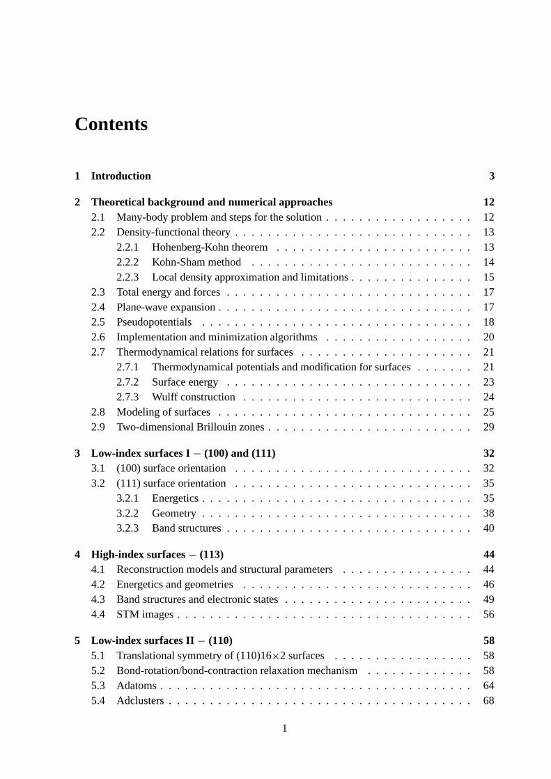
A typical example for the island formation is the Stranski-Krastanov (SK) growth mode[11, 17] of Ge on Si(100) substrates. The growth of a strained wetting layer, as thick as 3−4monolayers, is followed by the formation of three-dimensional islands. Eaglesham and Cerullo[18] have made the surprising discovery that in the initial stages of SK growth, the islands canbe coherent, i.e., dislocation-free. Only later, as the islands grow in size, dislocations develope.The coherent islands can be up to ∼ 150 nm in size and ∼ 50 nm high. Before the appearanceof micrometer-sized Ge crystallites, an intermediate phase of metastable clusters has been alsoobserved [19]. Scanning tunneling microscopy (STM) at low Ge coverage has shown that smallislands (so-called hut clusters [19] or pyramids [20]) with rectangular or square base are formedby {501} facets. Phase transitions take place when larger islands with a higher aspect ratio,so-called domes [21, 22], appear at higher Ge coverages and display a multifaceted surfaceincluding {311} facets. Typical Ge nanocrystals with both pyramid and dome shapes grownon Si(100) examined by STM are shown in Fig. 1.1 (from Ref. [21]). The situation may bemore complicated due to intermixing. Recently, it has been shown [23] that domes contain a
1. Introduction 5
Figure 1.1 STM topograph of Ge nanocrystals on a Si(001) surface showing both pyramids anddomes (from Ref. [21]).
Si-rich core covered by a Ge-rich shell. In any case nanocrystals are bounded by facets whichcorrespond to certain surface orientations. Faceted islands have been also grown on Si(111) [24]and SiC(0001) substrates [25], where {113} facets are quite pronounced.
The situation is less clear for Si nanocrystals. Micrometer-scale Si droplets have beenformed on a Si(111) substrate by photolithography [26]. They have been used to determinethe equilibrium shape of a small Si crystal. Well-characterized {111} and {311} facets exist onthe nanocrystal surface. They are separated by rounded regions that display a tangential merginginto the facets. Bermond et al. [26] found that the surface energy increases from {100} to {111}via a {311} plane, and has local minima at the surfaces {111}, {311}, {110}, and {100}. Theseresults are in qualitative agreement with measurements [27] of small voids in a Si crystal whichindicate the existence of the same facets. Pyramidal Si nanocrystals can be selectively grownon Si(100) windows in ultrathin SiO2 films [28–31]. These Si pyramids possess four equiva-lent facets of the types {111}, {311} or even {911} and {1 3 11}. Using a micro-shadow masktechnology or nonplanar prepatterned Si(100) substrates, the self-assembling Molecular BeamEpitaxy (MBE) growth also leads to nanometer-scale features [32]. Depending on the growthparameters, pyramid-like tips or long wedges are formed. The sidewalls are free-standing {111}and {311} facets.
One more group-IV material, diamond (tetrahedral carbon), possesses extraordinary prop-erties, which suggest a broad range of scientific and technological applications. Diamond is thehardest and stiffest material known, has the highest room temperature (RT) thermal conductiv-ity and one of the lowest thermal expansion coefficients of known materials. It is radiation-hardand chemically inert to most acidic and basic reagents. Diamond has a large band gap, henceelectrical devices can work at higher temperatures (HTs) than Si. Unfortunately, due to the highcost and preparation difficulties, the applications of natural and synthetic diamond have beenlimited in comparison to its great potential [33].
The many ways in which diamonds have been synthesized are clues to the conditions underwhich diamonds form naturally. Diamond is the stable carbon phase at pressure p > 5 GPa.Industrial-scale production of diamond starts from amorphous carbon or graphite at HT (1200–1400 ◦C) and high pressure (HP) (5 to 7 GPa). Diamond morphologies vary as a function oftemperature at constant pressure (for example, 6 GPa): Octahedrons form preferentially at HTs

1. Introduction 6
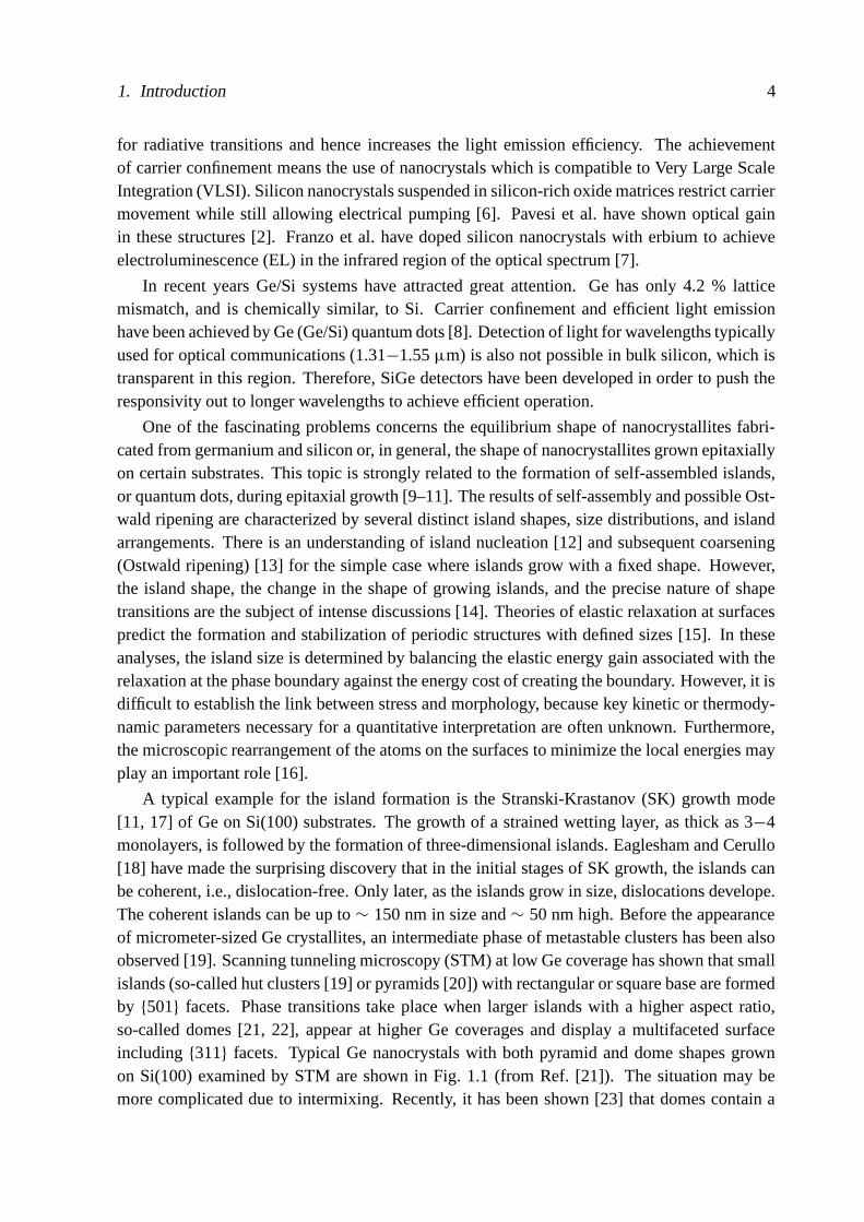
Figure 1.2 Micrograph of HP-HT synthetic diamond (left) and map of growth sectors (right)(from Ref. [34]).
1500 to 1600 ◦C, cubo-octahedrons at 1350 to 1500 ◦C, and cubes at <1300 ◦C. Small syntheticdiamonds grown by HT-HP methods have major growth sectors of {100} and {111} type andsome minor sectors of {110} and {311} (see Fig. 1.2) [34]. The most recent industrial method isto form diamond through Chemical Vapor Deposition (CVD). In this process, a thin (nanometerto micrometer) metastable diamond film is formed on metal substrates from methane (CH4)or other hydrocarbons at low pressure (<1 Pa) and at HT (1000 ◦C), in the presence of excesshydrogen. The morphology of diamond particles grown by HT-CVD is dominated by {100}and {111} facets (see Ref. [35] and references therein). In addition, facets of the types {110}and {311} appear between those with common orientation. However, it is difficult to concludethat {311} facets exist in a steady state. Using CVD also diamond nanocrystallites can begrown partially epitaxially or perfectly heteroepitaxially on stepped Si substrates with [110]orientation [36]. An exact determination of the facet orientations of the crystallites with 2–6 nmsize is, however, hardly possible.
The absolute value of the surface free energy of a crystalline solid is one of the most impor-tant fundamental quantities which characterizes a large number of basic and applied phenom-ena. Among them are crystal growth, surface faceting, epitaxy and stability of thin layers, andthe shape of small crystallites. In particular the construction of the equilibrium crystal shape(ECS) requires the complete determination of the surface free energy γ as a function of thesurface orientation n. Despite its significance, a complete and well-accepted set of correspond-ing experimental data of group-IV materials is not available. There are only few experimentaldata for surface free energies and only for Si [27]. In general, the experimental determina-tion of γ remains a challenge [37]. Theoretical data, in particular derived from highly-precise,parameter-free total-energy calculations, are of great importance. However, calculated absolutesurface energies are also rare.
Due to surface formation, bonds are cut, what requires energy. One may expect that theresulting surface energy γ is proportional to the dangling-bond density. However, in order toreduce this energy surface atoms relax which leads to a certain distortion of the ideal bulk-likepositions. Such processes take place in particular on metal surfaces. The situation for semi-conductors is more complicated due to the tendency of significant surface reconstructions. In

1. Introduction 7
tetrahedrally bonded semiconductors, such as diamond, Si, and Ge strong directional bonds arepresent what leads to dramatic effects. Nearly all surface orientations of group-IV elementsobserved experimentally possess reconstructions which give rise to a two-dimensional transla-tional symmetry with unit cells much larger than 1×1, i.e., that of a surface according to thebulk termination. It is required to understand and determine the precise atomic geometry of agiven reconstruction for a certain orientation depending on the material.
Calculations of absolute surface energies are mainly restricted to semi-empirical methodsas the tight-binding (TB) approach [38] or the use of classical interaction potentials [39, 40].In most cases they do not consider surface reconstructions. The fully quantum-mechanicaltreatment usually gives relative surface energies for different reconstructions but one and thesame orientation. Only for low-index diamond surfaces there are comparative studies whichgive absolute surface energies [41, 42]. Moreover, reconstruction elements which appear ongroup-IV surfaces are still under debate even considering low-index surfaces. The situation isreally complicated for Si and Ge surfaces. The origin and the driving forces of reconstructionsare not always understood. For that reason the main part of the present work is devoted tocomprehensive studies of diamond, Si and Ge surfaces including low-index (100), (111), (110)and high-index (113) ones. We try to answer the question as to why surfaces of group-IV ele-ments behave differently. There are no comprehensive comparative studies of the materials fordifferent surface orientations considering reconstructions observed experimentally. As a conse-quence, surface energies have not been determined and the energy dependences of the surfacereconstructions and orientations for these important semiconductors have not been derived.
Based on well converged energies of the most-frequently observed (100), (111), (110), and(113) surfaces of group-IV semiconductors one may construct the ECSs using the Wulff con-struction [43]. However, Wulff constructions using theoretical or reliable experimental datafor γ have not been presented so far for diamond, Si, and Ge. Yet important conclusions canbe drawn from the equilibrium shapes of the crystals. We attack this problem assuming largefacets. Therefore surface reconstructions are important. The stability evaluation of a certain sur-face orientation gives information about tendencies for faceting etc. For instance, the questionhas to be answered whether the ECS of diamond exhibits only cleavage orientations correspond-ing to {111} facets? Another one is if there are tendencies for high-index surfaces to contributeto the ECSs of Si and Ge?
In contrast to free crystallites the actual three-dimensional shape of a nanocrystal grown ona certain substrate depends on many thermodynamic and kinetic aspects or growth conditionsincluding strain, alloying, temperature, number of adsorbate atoms, wetting layer, and interface.For nanocrystallites grown (hetero)epitaxially, strain may play a dominant role for the crystalliteshape [9, 44]. Nevertheless, interesting trends can already be derived studying the influence ofsurface energies. We restrict the discussions of the shapes on the latter. Despite such a simplifiedpicture it could describe the trend for crystallites to be deformed if a certain base orientation anda certain shape are chosen. Pyramid shapes observed during the growth should be consideredand compared with ECSs (i.e., shapes of free crystallites).
The most powerful tools to study the energetics and the atomic geometry of solids andtheir surfaces are ab-initio methods, particularly using the Density-Functional Theory (DFT)

1. Introduction 8
for total-energy calculations. Parameter-free quantum-mechanical calculations can give a pre-cise microscopic picture of systems in the ground state. The true bonding behavior allows todetermine the electronic structure and consequently to come close to the understanding of thenature of studied surface reconstructions.
It is now generally accepted that the (100) surfaces of diamond, silicon, and germaniumshow dimer-based reconstructions [45, 46]. Symmetric dimers (SDs) dominate a 2×1 recon-struction of the C(100) surface [47]. At RT, Si and Ge exhibit a 2×1 reconstruction governed byasymmetric dimers (ASDs) [48]. A staggered arrangement of these dimers explains the c(4×2)low-temperature (LT) phase [46]. Recently, however, the atomic configuration of the Si(100)surface at very low temperature became a subject of debate. That concerns on the one hand thequestion whether the true surface ground state shows symmetric or asymmetric dimers. On theother hand, phase manipulation between c(4×2) and p(2×2) has been performed at 4.2 K usingthe STM [49]. The dimers were found to prefer the p(2×2) ordered phase when scanned witha negative tip. Applying a voltage pulse or scanning with a positive tip tends to reverse p(2×2)to c(4×2). Similar effects have also been observed on Ge(100) surfaces [50].
The origin and nature of reconstructions at (111) surfaces of elemental semiconductors isone of the most intensively discussed issues in surface physics. The (111) surfaces of diamond,silicon, and germanium show a manifold and puzzling reconstruction behavior in dependenceon the surface preparation and the considered semiconductor. Silicon and germanium exhibita 2×1 reconstruction following cleavage perpendicular to the [111] direction at RT. However,such a 2×1 reconstruction can be also found on the C(111) surface after careful preparation [46].From many experimental and theoretical studies the (111)2×1 surfaces are believed to have aπ -bonded chain geometry [51]. In the case of Si and Ge the π -bonded chains are tilted [52, 58]whereas, apart from one exception [53], converged total-energy calculations do not indicateneither a chain buckling nor a chain dimerization for diamond(111) [41, 54, 55]. For Si andGe the π -bonded chain reconstruction has two different isomers with the tilt angle of the up-permost chains in opposite directions [56–58]. The chain-left isomer has been indeed observedfor Ge(111)2×1 by means of scanning tunneling microscopy (STM) [59]. Heat treatment ofcleaved Si(111) and Ge(111) surfaces at elevated temperatures cause the 2×1 reconstructionto convert into a 7×7 (Si, [60]) and a c(2 × 8) (Ge, [61]) structure, respectively. Whereas theSi(111)7×7 surface is now explained by a dimer-adatom-stacking-fault (DAS) model with cor-ner holes [62–65], the Ge(111)c(2×8) surface is represented by a simple adatom model [66, 67].Recently, it has been shown that a c(2×8) reconstruction can be also observed on the quenchedSi(111) surface [68, 69].
There are various ab-initio studies of the basic reconstruction models, the π -bonded chainmodel for 2×1 [41, 53–56, 58], the DAS model for 7×7 [64, 65], and the adatom model forc(2 × 8) [67, 69]. However, there is no study by one and the same group and one and the samemethod of all reconstructions for even one semiconductor, not to speak about the three group-IVmaterials under consideration. Therefore, a comparison of the energetics and the driving forcesof the reconstruction is hardly possible. Precise conclusions, why the lowest-energy reconstruc-tions 2×1, 7×7, and c(2 × 8) of diamond, silicon or germanium are different, cannot be drawn.Obviously, despite the same valence-electron structure of the atoms and the same crystal struc-

1. Introduction 9
ture of the corresponding solid, the different atomic sizes and bonding characteristics give riseto a stabilization of different surface reconstructions. An explanation based on first-principlescalculations is, however, still missing. There are only model considerations comparing the en-ergetics of 7×7 and c(2 × 8) reconstructions [70].
Among the clean low-index silicon and germanium surfaces, the (110) surfaces are the onlyones whose atomic structures are unknown. Only for diamond(110), Low-Energy ElectronDiffraction (LEED) found a 1×1 diffraction pattern [71], the atomic structure of which canbe characterized by relaxation. At least for silicon, the (110) surface has a free energy onlyslightly larger than that of the (111) plane [27]. It should therefore be a stable facet on theequilibrium crystal shape [44]. However, the preparation of such surfaces is difficult. Onlynon-vicinal, clean and well-annealed Si(110) surfaces exhibit a 16×2 reconstruction [72–75].Contaminations, for example of very small amounts of Ni, destroy the long-range reconstructionand give rise to translational lattices with smaller unit cells, e.g. 5×1 [74, 76, 77]. STMexperiments [73–75] suggest that the Si(110)16×2 reconstruction consists of equally spacedand alternately raised and lowered stripes lying along the [112] direction. The height of thesteps between two stripes is equal to the layer spacing in normal direction. Along the stripesthese experiments reveal arrangements of “pairs of pentagons” which are more pronounced inempty-state images [75]. The experimental situation is less clear for the Ge(110) surfaces. Inthe pioneer’s work Olshanetsky et al. [78] showed that a c(8×10) superstructure appears afterannealing. Despite the existence of STM images for Ge(110)c(8×10) [79], there are indicationsthat the c(8×10) structure is transient and unstable and changes into a 16×2 superstructure [80,81]. However, for both periodicities the STM images show sequences of pentagons similar tothe findings for the Si(110) surface.
There are no accepted structural models for the reconstructed Si and Ge(110) surfaces whichconsistently explain the energetics, the geometry and the electronic structure, in particular theSTM images. Usually a certain distribution of adatoms and several top layers involved in thereconstruction are assumed in order to interpret the atomic structures of Si(110)16×2 [72, 75,82, 83] and Ge(110)c(8×10) [79] or 16×2 [80, 81]. Conglomerates of adatoms which captureinterstitial atoms like in the case of Si(113) surfaces [84] have been suggested by An et al. [75] toexplain the pentagon pairs observed in high-resolution STM images of the Si(110)16×2 surface.The origin of the stabilization of Ge(110) surfaces by certain reconstruction elements is also notunderstood. Recently, Ichikawa [81] explained the STM images observed for the Ge(110)16×2surface by pairs of five-membered adclusters. However, such structures are questionable fromthe energetical point of view.
Apart from one trial [81], theoretical studies have not been performed for the large 16×2or c(8×10) unit cells. Some attempts were devoted to find favorable reconstruction elementsand to understand the bonding behavior by studying smaller unit cells [83, 85, 86]. In par-ticular, it has been found that a bond-rotation relaxation mechanism should take place on Siand Ge(110) surfaces [85, 86] where the top-layer atomic chains are buckled like in the caseof III-V compounds [44]. Dimerization similar to the (100) case has been proposed based onTB calculations [83]. Possible structures with adatoms have been studied by means of bothab initio [86] and TB molecular-dynamics calculations [85]. The suggestion of fully bonded

1. Introduction 10
(i.e., fourfold-coordinated) adatoms which leave no dangling bonds [85, 86] is rather surprisingfor group-IV semiconductor surfaces and needs additional studies. In order to understand theatomic geometry and the bonding of the Si(110)16×2 surface, one has to study the energeticpreference and the structure of the step configuration observed by STM. Until now there is noidea why steps may occur on a flat, non-vicinal low-index surface, and how they contribute tothe stabilization of the 16×2 translational symmetry. First-principles calculations exist only forthe Ge(110)16×2 surface [81]. They suggest a higher surface energy when steps are introduced,in contrast to the experimental observations of images in form of stripes on lower and higherterraces also for germanium [79].
High-index (113) surfaces of group-IV semiconductors are of interest from both the funda-mental and applied point of view. In recent years wide flat (113) terraces have been prepared onSi substrates demonstrating that such surfaces are thermally stable against faceting [27]. Theirinherent structural anisotropy makes (113) surfaces promising substrates for epitaxial growthof novel optoelectronic devices [87]. Very interesting is the fact that {113} facets have beenobserved on islands for all group-IV materials.
The actual atomic structure of the (113) surfaces is also strongly changed by the surfacereconstruction. For Si and Ge, 3×1 and 3×2 translational symmetries have been reported [84,88–108]. To our knowledge there is neither a theoretical nor a direct experimental study ofclean reconstructed C(113) surfaces. The Si(113) surface exhibits a 3×2 reconstruction at RT,while a transition to the 3×1 phase is observed at elevated temperature [91, 94, 96, 104, 105].In the Ge case 3×2 and 3×1 periodicities seem to coexist already at RT [95, 99, 108].
The bulk-terminated (113) surfaces of diamond-structure crystals consist of alternating rowsof twofold-coordinated (001)-like atoms and threefold-coordinated (111)-like atoms. If one(001)-like atom is removed, the adjacent (111)-like atom looks like an adatom . The additionalformation of a tetramer by bonding two (001)-like atoms leads to a 3×1 translational symmetry[88]. Many refinements of such an adatom-dimer (AD) model, including voids, puckering andbuckling, and vertical displacement of the dimers, have been discussed to explain the observed3×2 translational symmetry, particularly for Si [88, 89, 98, 101–104, 106]. One importantstep towards the understanding of the behavior of group-IV(113) surfaces was the introductionof a novel reconstruction element, a sixfold-coordinated surface self-interstitial similar to the[110]-split interstitial bulk defects, by Dabrowski et al. [84, 92, 107]. Interstitial distributionand migration [95, 107, 108] allow the study of additional surface reconstructions, among themadatom-interstitial (AI) and adatom-dimer-interstitial (ADI) models.
Meanwhile, there are several ab initio studies of 3×1 and 3×2 reconstructions of Si andGe(113) surfaces [84, 106–110]. There are also studies using a semiempirical method [111] orcombined methods [106]. However, the energetical ordering of the most important structuralmodels is not well clarified for both Si and Ge [92, 106, 108]. Details of the geometrical re-constructions concerning their asymmetries, e.g. buckling, puckering, vertical displacement ofappearing reconstruction elements, tetramers or pentamers, are under discussion. The chemicaltrends in energies and geometrical parameters are not understood. This holds for the compar-ison between Si and Ge(113) but, in particular, for C(113); the properties of this surface areunknown.

1. Introduction 11
The driving forces of the various reconstructions have not yet been understood completely.The relationship between energetics, bonding, displacements of atoms, and the electronic struc-ture is not clarified. There are only a few simulated images observable in STM [84, 92, 106,107]. However, their relation to the surface band structures and surface electronic states isnot derived. Calculated band structures are not published, except from those derived within aTB approach [106], the accuracy of which is, however, limited. The experimental bands forSi(113)3×2 need an interpretation [102]. It has to be discussed why 3×1 reconstructions areseemingly observed in several experiments, despite the violation of the general reconstructionrules [112] and the electron counting rule [113]. Consequently, the metallic or insulating char-acter of a (113) surface has to be explained in dependence on the translational symmetry butalso the (local) point-group symmetry.
Then questions are addressed in the thesis at hand in the following way: Descriptions of thetheoretical grounds and numerical approaches are given in Chapter 2. The studies of drivingforces and the energetics of diamond, Si and Ge surfaces are presented in Chapter 3 for 〈100〉and 〈111〉 surface orientations. Chapter 4 is devoted to the 〈113〉 surface orientation, whereasChapter 5 focusses on the 〈110〉 surface orientation. A discussion of shapes of free and con-strained crystallites based on the calculated absolute surface energies is given in Chapter 6.Summary and conclusions follow in Chapter 7.
Chapter 2
Theoretical background and numericalapproaches
2.1 Many-body problem and steps for the solution
The theory of solids including their surfaces leads to a complicated microscopic description ofinteracting atoms. Formally the Hamiltonian H of any system consists of kinetic and Coulombinteraction energy contributions of all nuclei and electrons involved. The properties of thesystem can be derived by solving the many-body Schrödinger equation:
H9 = E9, (2.1)
where the wave function 9 depends on the coordinates of electrons r and nuclei R. However,the solution of problem (2.1) is almost impossible because of its complexity. One needs tosearch for (some) approximations. One idea arises from the difference of the involved particles.The motion of nuclei is much slower than that of the electrons. Therefore, movements ofthe electrons and nuclei can be separated. The motion of the electrons is determined for theensemble of nuclei at certain fixed positions. The resulting total energy of the electrons togetherwith the ion-ion repulsion gives rise to a potential surface for the motion of the nuclei. Usingthe Born-Oppenheimer adiabatic approximation, the total wave function can be represented asa product of the ion and electron wave functions [114]. For the ground state of the electronicsystem one has to solve the Schrödinger equation for the many-electron Hamiltonian
Hel = −∑
i
h2
2m∇2
i −∑
l,i
Zle2
|ri − Rl |+ 1
2
∑
i 6= j
e2
|ri − r j |, (2.2)
where the three terms represent the kinetic energy of electrons Tel, the interaction energy withthe external potential Vext imposed on the electrons for a given nuclear configuration, and theCoulomb energy of interacting electrons Uee, respectively. Spin is not considered. The prob-lem of the Hamiltonian (2.2) is still very difficult to solve. While Tel and Vext depend only onthe i -th electron, Uee involves pairs of electrons. According to Hartree a simplification can beachieved by writing the many-electron wave function as a product of one-electron wave func-tions ψi (ri ), 9 =
∏
i ψi (ri ), which leads to an effective one-electron Schrödinger equation.
12

2.2. Density-functional theory 13
Such a simple product ansatz describes non-interacting particles. Since we have interactingparticles it is only an approximation, implicitly assuming that adding an interaction to the non-interacting system does not significantly change the wave function. However, this is not the onlyweakness of this ansatz. The Hartree approximation needs to be improved upon by introducingPauli’s principle using an antisymmetric many-electron wave function in the form of a Slaterdeterminant [115]. This is the idea of the Hartree-Fock (HF) approximation which introducesthe spatially nonlocal electron exchange [116, 117]. The HF method requires already heavynumerical treatments, despite the fact that it does not take into account correlation effects. Cor-relation is, in fact, defined as the missing part of the HF electron-electron interaction comparedto the exact solution. The HF method is usually only suitable for systems with not too manyelectrons. Because of neglecting correlation, it works better for atoms and molecules. In thecase of solids such as metals and semiconductors, bonding and electronic properties are notreproduced correctly by the HF method. The inclusion of correlation effects using the so-calledconfigurational interaction (CI) method is restricted to small molecules. Here, a sum of Slaterdeterminants is needed which has to be truncated in practical calculations. Only such sums ofSlater determinants allow an exact representation of any arbitrary wave function of a true in-teracting systems, whereas single Slater determinants are only exact in the case of systems ofnon-interacting particles.
2.2 Density-functional theory
A theory for the description of a system with many electrons including correlation effects isthe Density-Functional Theory (DFT). It is based on the theorem of Hohenberg and Kohn thatthe ground-state energy is a functional of the electron density only [118]. A practical methodfor treating inhomogeneous systems of interacting electrons has been proposed by Kohn andSham [119] and makes the DFT an extremely powerful tool for the determination of propertiesof matter using a microscopic model according to e.g. Eq. (2.2).
2.2.1 Hohenberg-Kohn theorem
This theorem is usually formulated for an external potential Vext(r) acting on a system of Nelectrons, which could be for instance the potential of an electron in the field of all nucleiwhich therefore depends on the configuration of the nuclei [cf. e.g. Eq. (2.2)]. The electrondensity n(r) determines the ground state energy E[n] of the system no matter what the externalpotential is. It has been proven by reductio ad absurdum that Vext(r) is a unique functional ofn(r). The knowledge of the total density n(r) is as good as the knowledge of the wave function9 describing the ground state of the system. Since for a non-degenerate ground state 9 is afunctional of n(r) [120], so are evidently also the resulting kinetic and interaction energies. Fora given potential Vext(r), the energy functional can be written as
E[n] =∫
Vext(r)n(r)dr + F[n], (2.3)

2.2. Density-functional theory 14
where F[n] is an universal functional which contains the total effect of the electron-electroninteraction. For the density n(r) that minimizes the functional (2.3), E[n] equals the groundstate energy E0. Thereby the admissible densities are restricted by the condition of particlenumber conservation
∫
n(r)dr = N . (2.4)
The ground state density can be calculated, in principle exactly, using a variational methodinvolving only the density. To determine n(r) one finds
δ
{
E[n] − µ
[∫
n(r)dr − N
]}
= 0, (2.5)
where µ is a Lagrange multiplier which may be interpreted as the chemical potential of theelectrons. From Eq. (2.3) one obtains now
δE[n]δn(r)
= Vext(r)+ δF[n]δn(r)
. (2.6)
The major part of the complexities of the many-electron problem is now deferred to the deter-mination of the universal functional F[n].
2.2.2 Kohn-Sham method
In analogy to the Hartree or the HF approximation, it was proposed to separate the total energyin the components
E[n] = Ts[n] +∫ [
Vext(r)+ 1
2VH(r)
]
n(r)dr + Exc[n], (2.7)
where Ts[n] is the kinetic energy of a non-interacting electron system which has the same den-sity n(r) as the real interacting system. The classical Coulomb interaction between the electronsis described by the Hartree potential
VH(r) = e2∫
n(r′)
|r′ − r|dr′ (2.8)
which includes self-interactions. The factor 1/2 avoids that pair interactions are counted twice.The external potential Vext in Eq. (2.7) is due to the nuclei, and Exc is the exchange-correlationenergy. The last term includes all the interaction contributions missing in the previous terms,i.e., electron exchange and electron correlation, a portion of the kinetic energy which is neededto correct Ts[n] to obtain the true kinetic energy of the real interacting system, and correctionsto compensate the self-interactions introduced by the classical Hartree interaction. Accordingto Eq. (2.6) one has
δE[n]δn(r)
= δTs[n]δn(r)
+ Vext(r)+ VH(r)+ δExc[n]δn(r)
. (2.9)

2.2. Density-functional theory 15
The last three terms can be expressed by an effective potential Veff, and a Schrödinger-likeequation of noninteracting particles has to be solved. The so-called Kohn-Sham (KS) equationis
[
− h2
2m∇2
i + Veff(r)
]
ψi (r) = εiψi (r). (2.10)
It describes an auxiliary system of non-interacting particles, the density of which is equal to thedensity of the real interacting system. The ground-state density n(r) is derived from the wavefunctions,
n(r) =occ.∑
i
|ψi (r)|2. (2.11)
The KS Eq. (2.10) has to be solved self-consistently. After subtraction of doubly counted termsthe total ground-state energy can be expressed as
E[n] =occ.∑
i
εi − 1
2
∫ ∫
n(r)n(r′)
|r − r′| drdr′ −∫
Vxc(r)n(r)dr + Exc[n] (2.12)
where Vxc(r) = δExc[n]δn(r) is the exchange-correlation potential. Wave functions and densities
depend parametrically on the atomic coordinates.
2.2.3 Local density approximation and limitations
The exchange-correlation energy Exc[n] in the KS equation (2.10) can be written in the form
Exc[n] =∫
exc[n, r]n(r)dr (2.13)
where exc[n, r] is an exchange-correlation energy density per particle. In the local densityapproximation (LDA) exc[n, r] is replaced by the exchange-correlation energy of the homoge-neous electron gas, ehom
xc (n), where the constant density is replaced by the local density of thestudied inhomogeneous electron gas. It results in
Exc[n] '∫
ehomxc (n)
∣
∣
∣
n=n(r)n(r)dr. (2.14)
For ehomxc there are several prescriptions available in the literature. The exchange part can be
calculated analytically. For the correlation part, values have to be taken from numerical calcu-lations. In the present work the Ceperly-Alder results [121] based on Monte-Carlo calculationsand parameterized by Perdew and Zunger [122] are used.
Despite the fact that the LDA is a crude approximation for a strongly inhomogeneous gas, itis even able to predict bonding properties of solids with covalent bonds. There are quantitativeerrors in the evaluation of bond lengths, elastic constants, and cohesive energies which are in

2.2. Density-functional theory 16
principle known, and often the situation can be improved by using the generalized gradient ap-proximation (GGA) [123]. Within the LDA one finds an overbinding tendency: The calculatedcohesive energies come out larger compared to experiment, while lattice constants and bondlengths are smaller. In the case of Si, the lattice constant is 5.398 A within LDA or 5.464 Awithin GGA, while measurements give the value 5.431 A [124]. It is also expected that absolutesurface energies within GGA are somewhat lower than those calculated within LDA because ofthe larger cohesive energies obtained for the latter case.
Measurements such as photoelectron or inverse photoelectron spectroscopies are frequentlydirected to the determination of the electronic bands in a crystalline solid. Comparing with theKS eigenvalues in (2.10) in particular, the band dispersion is reasonably described. There is noclear justification for interpreting the one-particle eigenvalues in DFT as the band structure. Thisis because the KS energies are eigenvalues of the auxiliary system of non-interacting particleswhich have a physical meaning only for its density and functionals of the density, like the totalenergy. Only the highest occupied level has a real physical meaning and is identical with thefirst ionization energy of an N-electron system. However, despite its lack of formal justificationas a description of band energies the KS scheme bears at least some merit for the descriptionof excitations [125]. DFT transition energies between occupied and empty states, includingthe fundamental gap, are clearly underestimated. The underestimation of the fundamental bandgap is a serious problem independent of the LDA or GGA treatment of the exchange-correlationenergy [126]. Within the DFT-LDA (GGA) one obtains about one half of the experimental bandgap for Si and C, and practically a zero gap in the case of Ge.
In order to obtain correctly the quantity corresponding to the experimental band gap onemay calculate quasiparticle energies by using the many-body perturbation theory and deter-mining the poles of the one-particle Green’s function G. One way to proceed is Hedin’s GWapproximation [127, 128]. It accounts for the response of the electronic system to an elec-tron or hole by screening. This leads to the occurrence of the screened Coulomb potentialW. Usually, it is sufficient to calculate only the discrepancy between the exchange-correlationself-energy 6xc = GW in this approximation with respect to the XC potential Vxc(r) =ehom
xc (n) + n ddn ehom
xc (n)∣
∣
n=n(r) already included in the KS Eq. (2.10). Within the first-orderperturbation theory it results in quasiparticle shifts of all KS eigenvalues which open the gapsand increase transition energies between valence and conduction bands.
However, in general the DFT-LDA method is sufficient for the major purposes of this disser-tation, in particular for studies of atomic structures of diamond, silicon and germanium surfacesin the ground state, and the second step, the evaluation of absolute surface energies since wefocus on comparative studies. The KS eigenvalues are only used to discuss qualitatively theelectronic structure of a surface,1 in particular their metallic or insulating character and the ap-pearance of bound surface states in the fundamental gap. Certain remarks will be given in thetext where surface electronic structures of Ge surfaces are discussed.
1The eigenvalues of the KS equation (2.10) are also used to simulate the STM images within the Tersoff-Hamann approach [129]. A constant-height mode is assumed for the simulation. Smearing-out procedures toaccount for the non-ideality of the tip are not used.
2.3. Total energy and forces 17
2.3 Total energy and forces
The KS approach allows the determination of the electronic ground-state energy of the systemfor a given nuclear configuration. The total energy of the system contains the electronic energy(2.7) and the energy of interacting ions:
Etot = 1
2
∑
I,J
e2 Z I Z J
|RI − RJ | + E[n], (2.15)
where the first term is the Coulomb repulsion energy of the nuclei. The force F I acting on theatom at the position RI can be obtained by the gradient
FI = −∇RI Etot. (2.16)
Etot depends explicitly on the coordinates of the nuclei. In addition, E tot also depends implicitlyon these coordinates via the charge density n(r). Consequently two different contributions tothe forces are obtained:
FI = −dEtot
dRI−
∫
�
δEtot
δn(r)dn(r)dRI
dr. (2.17)
The force contribution due to the explicit dependence on the energy on the atomic position iscalled the Hellmann-Feynman force [130, 131]. It is of physical origin, in contrast to the secondpart in Eq. (2.17). This part is called variational force [132] and vanishes in the ground state fora given configuration {RI }. We optimize structures until forces are smaller than 10 meV/A.
2.4 Plane-wave expansion
For the numerical treatment, it is advantageous to expand the KS eigenfunctions of Eq. (2.10) incertain orthonormalized and more or less complete basis sets. Since we apply the repeated-slabmethod [44] to model the surfaces, one has to handle an artificial system with huge unit cells.Because of a translational symmetry a system is expressed by the a Bravais lattice with latticepoints {R}. Consequently it can be expanded in terms of plane waves (PWs)
1√�
exp[i(k + G)r], (2.18)
where G is a reciprocal lattice vector with G · R = 2π times an integer number, and k is a vectorwithin the first Brillouin zone (BZ). The functions (2.18) form an orthonormal and complete setof wave functions. Performing calculations on periodic systems the KS orbitals in (2.10) withquantum numbers i = jk can be written as a sum of plane waves
ψ jk(r) = 1√�
∑
G
c j,k+Gexp[i(k + G)r]. (2.19)
The functions (2.19) fulfill the Bloch theorem. For numerical calculations, only a finite numberof k can be taken into account. Therefore, usually a set of so-called special k points that are

2.5. Pseudopotentials 18
adapted to the crystal symmetry is used [133–135]. An integral over k points is approximatedby a weighted sum:
(2π)3
�0
∫
BZf (k)dk =
∑
sp
wsp f (ksp) (2.20)
with �0 as volume of a unit cell and the normalization∑
spwsp = 1 for the weights. Inthe case of more than one k point, a rather simple but flexible method has been suggested byMonkhorst and Pack (MP) [134] where the set of k points is generated by division of the latticevectors of the reciprocal lattice into Pi equal pieces. Every mesh point represents a k point ofthe MP set. The points lying within the irreducible part of the BZ (IBZ) are finally used tocalculate quantities such as the electron density or the total energy with weights according totheir symmetry degeneracy. Hence, the number of k points depends on the size of the IBZ and,therefore, on the symmetry (see also Sect. 2.9).
The expansion of the electronic wave functions would in principle require an infinite plane-wave basis set. However, the coefficients ci,k+G for the plane waves with small kinetic energyh/2m|k + G|2 are typically more important than for those with large kinetic energy. Thus thePW basis set can be truncated to include only plane waves that have kinetic energies less thansome particular cutoff energy,
h
2m|k + G|2 ≤ Ecut. (2.21)
The energy Ecut has to be chosen in a way that, on the one hand, the wave functions maybe reasonably represented and, on the other hand, the numerical effort is not too large. Theconvergence has to be carefully tested.
With a plane-wave basis, the KS equation gives the secular equation:
∑
G′
[
h
2m|k + G|2δG,G′ + Veff(k + G, k + G′)
]
ci,k+G′ = εi ci,k+G, (2.22)
with the Fourier components Veff(k + G, k + G′) of the KS potential. The latter potential isnonlocal due to the use of nonlocal pseudopotentials. In the local case the Fourier componentsonly depend on differences of reciprocal lattice vectors, Veff(G − G′)) = Vext(G − G′)) +VH(G − G′) + Vxc(G − G′). In Eq. (2.22) the kinetic energy is diagonal, and the various po-tentials are described in terms of their Fourier transformations. The system (2.22) of algebraicequations has to be solved. The size of the Hamilton matrix which has to be diagonalized isdetermined by the choice of Ecut. It will lead to rather heavy calculations if the studied sys-tem contains both valence and core electrons. This problem can be overcome by the use of thepseudopotential approximation.
2.5 Pseudopotentials
The concept of pseudopotentials supplies smooth wave functions, which can be easily expandedin PWs. The core electrons do not contribute appreciably to the properties of interest and can
2.5. Pseudopotentials 19
be “frozen” in their free-atom configuration, while the bonding is dominated by the behaviorof the valence electrons. In particular, the Si atom consists of a nucleus (14+), core electrons[1s22s22p6] and valence electrons [3s23p2]. The idea is to map the all-electron problem ontoan equivalent problem involving valence electrons only. The consequences are (i) a frozen corewith the nucleus and the core electrons and (ii) smooth orbitals for the valence electrons [136].The formal transformation of the Hamiltonian is an orthogonalization to core states, givingpseudowavefunctions and pseudopotentials. It turns out that the orthogonalization “cancels”to a large extent the ionic attraction in the core region [137]. The pseudowavefunction of thelowest valence state is nodeless, and all the others are smooth as well. The ionic pseudopotentialconsists of a Coulomb attractive term, whose charge is the valence one, plus a short-range part,mostly due to non-classical orthogonalization repulsion, but which also has contributions fromthe true interactions with core electrons. In order to use the pseudopotential approach one hasto ensure that the core overlap between neighboring ions is negligible.
A step forward to modern pseudopotentials has been done by the introduction of the norm-conservation requirement, in particular for applications in solid-state physics [138]. In thisapproach, pseudowavefunctions are constructed. The potentials are then found by invertingthe atomic Schrödinger equation. Together with the matching conditions at Rcut the conceptof norm-conservation guarantees that the pseudocharge distribution exactly reproduces the fullvalence charge beyond the core radius. Such pseudopotentials are nonlocal, because the radialionic pseudopotential depends explicitly on the angular momentum. One more difficult problemhas to be solved for Ge which has an extended core, 1s22s22p63s23p63d10. In particular the3d-core shell is extended, partial overlap with valence electrons is possible. To include thiseffect partially one has to use the so-called nonlinear core corrections which correct errorsdue to the linearization of the exchange-correlation energy in the valence and core electrondensities [139, 140]. Si and Ge are best described using norm-conserving pseudopotentials.
There is still a problem for C atoms where the core only consists of the 1s electron shell. Formaterials with such a small core a good transferability can only be achieved by pseudopotentialswhich are very “hard” and consequently need a PW expansion restricted by a large cutoff inorder to achieve convergence in a given calculation. Ecut is required to be of about 700 eV ifnorm-conserving pseudopotentials are used [141]. Atoms such as carbon can be better masteredwithin the ultrasoft pseudopotential scheme proposed by Vanderbilt [142], tailored to generatepseudowavefunctions which are smooth, although the condition of norm-conservation is notused. The missing charge is accurately accounted for by an augmentation procedure in the self-consistent scheme. As a result, the ultrasoft pseudopotentials achieve both high transferability(adequate description of the scattering properties of the ion in diverse chemical environments)and fast PW convergence. We apply the ultrasoft pseudopotentials not only for carbon but alsofor silicon and germanium. The details of the pseudopotentials used in this work are given inTable 2.1. A more detailed description of the construction of the pseudopotentials used can befound in Refs. [142–144] and the references cited therein. As a consequence of the optimizationof the pseudopotentials the PW expansion of the single-particle eigenfunctions can be restrictedby an Ecut of only 270 (C), 130 (Si), and 120 eV (Ge). In Fig. 2.1 a series of test calculations isshown for the total energy Etot, lattice constant a0, and isothermal bulk modulus B0 versus Ecut.

2.6. Implementation and minimization algorithms 20
Table 2.1 Cutoff radii Rcut and types of pseudopotentials [ultrasoft (US), norm-conserving (NC), all
electron (AE)] for corresponding angular momentum (AM) for C, Si, Ge and H used in the calculations.
For hydrogen two types of pseudopotentials are used, Hsoft for Si-H and Ge-H bonds and Hhard for C-H
bonds. In the US case values in parentheses denote cutoff radii of the augmentation charges.
Element AM Rcut Potential Element AM Rcut Potential
C s 1.90(1.40) US Si s 2.35(2.00) US
p 1.90(1.40) US p 2.80(2.20) US
d 1.90 NC d 2.80(2.30) US
local dpot local 1.60 cut AE
Hsoft s 2.00(1.50) US Ge s 2.45(2.10) US
p 2.20(1.50) US p 2.90(2.30) US
local 1.0 cut AE d 2.80(2.30) US
Hhard s 1.25(0.80) US local 1.60 cut AE
p 1.25(0.80) US
local 0.65 cut AE
The figure indicates convergence of the ground-state properties for the chosen energy cutoffs.The resulting lattice constants a0, chemical potentials µ, and fundamental energy gaps Eg (thelatter ones are determined from bulk band structure calculations) are a0 = 3.531, 5.398, and5.627 A, µ = −5.195,−5.957, and −10.147 eV, and Eg = 4.15, 0.46, and 0.00 eV for C, Siand Ge in DFT-LDA.
2.6 Implementation and minimization algorithms
The investigation of the microscopic properties in the framework of DFT-LDA has been donewith the VASP (Vienna ab-initio Simulation Package) code (see Refs. [145, 146]). This com-plex package allows the minimization of the total energy with respect to both electronic andionic degrees of freedom. It also provides tools for generating and testing pseudopotentials ifnecessary. Most of the algorithms implemented in VASP use an iterative matrix-diagonalizationscheme: the employed algorithms are based on the conjugate gradient scheme [147, 148], blockDavidson scheme [149, 150], or a residual minimization scheme − direct inversion in the it-erative subspace (RMM-DIIS) [151, 152]. For the mixing of the charge density an efficientBroyden/Pulay mixing scheme [152–154] is used. The package VASP is available as a fully par-allel code. Together with the use of ultrasoft pseudopotentials and the effective minimization-schemes [145] it allows us to treat large systems, here artificial crystals with diamond, Si, andGe surfaces, with up to several hundred atoms in a unit cell.

2.7. Thermodynamical relations for surfaces 21
Figure 2.1 Convergence with respect to Ecut for bulk properties of C, Si, and Ge.
2.7 Thermodynamical relations for surfaces
2.7.1 Thermodynamical potentials and modification for surfaces
The equilibrium state of a one-component system consisting of N particles at a fixed tempera-ture T and pressure p is the one with the minimum Gibbs free enthalpy G(T , p, N ) [155],
G = F + pV, (2.23)
where F(T , V, N ),
F = U − ST , (2.24)
is the Helmholtz free energy. It is related to the internal energy U = U(S, V, N ) and the entropyS by a Legendre transformation. The energy conservation law and the relationship between heatand work can be written in the form
dU = T dS − p dV + µ dN (2.25)
for an infinitesimal change of the internal energy. A variation of the number of particles Nis allowed due to particle exchange with a reservoir characterized by the chemical potential µ

2.7. Thermodynamical relations for surfaces 22
of the particle. For an isolated system with no heat exchange (dS = 0) and particle exchange(dN = 0) the internal energy is a constant at constant volume (dV = 0).
The thermodynamical potential G (or F) can be used to derive the thermodynamical quan-tities of the considered system at constant temperature T , particle number N and pressure p (orvolume V ). Infinitesimal changes of the three variables give rise to infinitesimal changes of thepotential, so that
dG = −SdT + V dp + µ dN (2.26)
or
dF = −SdT − p dV + µ dN . (2.27)
In equilibrium, F is a minimum with respect to the inner variables at constant T , V , and N ,whereas G is a minimum at constant T , p, and N . The chemical potential µ in Eqs. (2.25),(2.26), or (2.27) is given by
µ =(
∂U
∂N
)
S,V=
(
∂F
∂N
)
T,V=
(
∂G
∂N
)
T,p. (2.28)
Under normal pressure of about 1 atmosphere, the difference between the Helmholtz freeenergy F and the Gibbs free energy G,
� = F − G = −pV, (2.29)
is insignificant for a bulk solid or liquid. This holds in particular for volume-induced changes−p dV . Thus, it is sufficient to use F for the most cases interesting in solid state physics. Thedifference (2.7) is Kramer’s grand potential� = �(T , V, µ) [156]. Despite its smallness, moreprecisely its vanishing influence on changes in the bulk systems including phase transitions, thepotential is convenient to use for system transformations that occur at a constant temperature T ,volume V , and chemical potential µ. This may be of particular interest for the surface regionof the systems under consideration. Together with the Gibbs–Duhem equation, SdT − V dp +Ndµ = 0, infinitesimal changes of the variables result in
d� = −SdT − p dV − Ndµ. (2.30)
The comparison of Eqs. (2.27) and (2.30) indicates a transformation law
� = F − µN . (2.31)
This is a consequence of the fact that the Gibbs free enthalpy varies linearly with the number ofparticles (cf. 2.29 and 2.31),
G = µN (2.32)
with the proportionality factor µ = µ(T , p) for each homogeneous phase [155].

2.7. Thermodynamical relations for surfaces 23
In order to discuss the influence of a free surface of a halfspace, we follow Gibbs’ idea of the“(equimolar) dividing surface” [156, 157]. It can be presented in terms of the particle densityn = N/V as a function of the distance normal to the surface. Values of n change gradually fromits solid to its vapor value. The total space is divided into a bulk solid volume V1, a bulk vaporvolume V2, and a volume Vs of the transition region, the surface. The corresponding densitiesn1 and n2 characterize the uniform bulk phases, the (semi-infinite) solid and its vapor withwhich the solid coexists and which occupies the other halfspace. The surface region, whosespatial extent is of atomistic dimensions (about 10 or less atomic layers), is thus a stronglyinhomogeneous region surrounded by two homogeneous phases, the solid and the vapor. Thenumber of particles in each phase 1 or 2 depends on the number of particles Ns in the surfacetransition region. The same holds for the volumes. This uncertainty is of the same order ofmagnitude as the surface effect itself. However, in the framework of a macroscopic theory, herethe thermodynamics, the partition is made unique by applying the natural conditions [155]
V = V1 + V2,
N = n1V1 + n2V2. (2.33)
In comparison to the total number of particles the number of particles Ns in the surface regionis assumed to be negligible. In the macroscopic limit it holds that Ns = 0.
The extensive thermodynamical potentials under consideration, the free energy F and thefree enthalpy G, can be written as contributions from phases 1, 2 plus a surface term. We followthe derivation of Landau and Lifshitz [155] as well as of Desjonqueres and Spanjaard [156] andconsider Kramer’s grand potential. Since in the thermodynamical equilibrium the pressure pis the same in the two homogeneous bulk phases, at least for a plane surface [155], equation(2.29) can be written in the form
� = −p(V1 + V2)+�s. (2.34)
The surface contribution�s to the grand potential should be proportional to the surface area A,
�s = γ A (2.35)
with γ as the surface excess density of �.
2.7.2 Surface energy
The proportionality factor γ in Eq. (2.35) can be identified as the surface excess free energyper unit area or surface free energy for short (but imprecisely). For a one-component systemthe chemical potential µ is equal in both phases in the thermodynamical equilibrium. With thetotal number of particles according to Eq. (2.33), G = µN Eq. (2.26) is still fulfilled. From theapproximate description of the “dividing surface” with Ns = 0, one readily obtains Gs = 0 forthe surface contribution. Thus, with Eq. (2.35)
Fs = �s = γ A (2.36)

2.7. Thermodynamical relations for surfaces 24
Figure 2.2 Example for the determination of the ECS from the Wulff construction.
holds. The surface excess free energy γ is sometimes called surface tension, although this termis somewhat confusing despite the corresponding common unit of measurement.
The calculation of the surface free energy for a given surface orientation [hkl] and surfacereconstruction is described in detail in Sect. 2.8. Here we assume zero temperature (or at leasta thermal energy small compared to the energy barrier between two reconstructions) and thatthe crystal is unstrained. The calculations are restricted to the electronic configuration. Thecontribution of the zero-point displacements of the lattice is neglected. Only the core-corerepulsion is taken into account and the system energies are calculated using expression (2.15).
2.7.3 Wulff construction
The anisotropy of the surface free energy per unit area, γ (hkl), with the orientation of a certainsurface {hkl} determines the equilibrium shape of small free crystals at a particular temperatureT (here: T small compared to the melting temperature). Wulff and later Herring [43, 158, 159]have derived a thermodynamic theory for the equilibrium shape of small crystals in the case thatthe energies γ (hkl) for all facets, i.e. the relevant surface orientations 〈hkl〉, are known. It isbased on the relation (2.36) for unstretched surfaces. The crystallite is assumed to be of at leastmesoscopic or nanometer size so that edge and apex effects (more precisely, the correspondingenergy terms) can be neglected (compared to the surface energy terms). Then, the equilibriumcrystal shape (ECS) at constant (here: low) temperature T with fixed crystal(like) volume V andchemical potentialµ of the group-IV material is determined by the minimum surface excess freeenergy Fs with respect to the total surface area A = A(V ) of the crystal,
Fs =∫
A(V )
∫
© γ (hkl)d A, (2.37)
subject to the constraint of fixed volume V ,
V =∫
V (A)
∫∫
dV . (2.38)

2.8. Modeling of surfaces 25
The direction n of the area element d A is parallel to the facet normal 〈hkl〉. In the case of pureenergetical studies of nanocrystals with pyramidal shape one has to take into account additionalconstraints such as the orientation and the shape of the basal plane of the pyramid. Formula(2.37) represents a bridge between microscopic and macroscopic approaches to the propertiesof matter. The surface free energies γ (hkl) based on a full quantum-mechanical treatment of themotion of electrons (as discussed below) are combined to calculate a thermodynamic potentialwhich is minimized with respect to the shape of a crystallite.
The Wulff theorem based on the minimum surface excess free energy (2.37) and the con-straint (2.38) [43, 158, 159] states that the ECS is not necessarily that of the minimum surfacearea of the free crystallite. It may be a complex polyhedron with the lowest total surface energyfor a given volume. A minimal surface area occurs only for perfectly isotropic (i.e., constant)values of γ (hkl). The corresponding ECS is a sphere. The variation of γ with the normal n‖ 〈hkl〉 produces, on each surface element d A, a force proportional to ∂γ /∂n which tends toalter the direction at the same time as γ tends to shrink the area. Consequently, in general theECS cannot be a sphere. Determination of the ECS from the Wulff construction is equivalent tosolving r(h) = minn(γ (n)/n · h), where r(h) is the radius of the crystal shape in the directionh. A two-dimensional example of the Wulff construction is presented in Fig. 2.2. In a polar(spherical for 3D case) coordinate system, draw a vector parallel to the normal of the surfaceand with length proportional to the energy of the surface γ (n). For each of the vectors draw theperpendicular line. The ECS is described by the interior envelope of these perpendicular lines(planes).2
2.8 Modeling of surfaces
In order to model the various surfaces we consider periodic arrangements of slabs along thesurface normal. Each slab consists of a certain number of atomic layers and a vacuum region.Within one supercell the number of atoms in one layer is restricted to the surface unit cell. Thereare two types of possible slabs, centrosymmetric and asymmetric ones. In the first case twoidentical surfaces are involved as can be shown by applying a space-group transformation. In thesecond case one side of the material slab in the unit cell is saturated by hydrogen atoms as shownin Fig. 2.3. In our studies we use both types. While centrosymmetric slabs are used in orderto obtain accurate absolute surface energies, the ones passivated by H and with substantiallyreduced number of layers are used to study surface reconstructions and accompanying bandstructures. Relative surface energies are also obtained by using asymmetric H-covered slabsas described below. They allow the calculations of relative surface energies for reconstructedsurfaces with respect to a surface with a bulk orientation. The combination of such values withabsolute surface energies of unreconstructed surfaces gives the absolute surface energy of areconstructed surface.
2In the present work the program Wulffman for interactively examining the Wulff shapes of crystals is used[160].

2.8. Modeling of surfaces 26
Figure 2.3 Examples for models of centrosymmetric (left) and asymmetric (right) slabs of(111) surfaces. Together with the vacuum region along the [111] direction the material slabs arerepeated according to the translational symmetry. Two surfaces, an upper one and a lower one,
occur for each system.
The two surfaces of a centrosymmetric slab are physically equivalent and, hence, allow thedirect calculation of absolute (free) surface energies. As an advantage, in the centrosymmetriccase the same surface and, hence, the same surface reconstruction n × m occurs on both sidesof a material slab. For a given atomic configuration {Ri} in such a slab the surface energy (per1×1 surface cell) can directly be inferred from the total energy of the slab E tot(N , {Ri }) withN atoms by subtracting N times the bulk energy µ per atom,
En×msurf = 1
2nm{Etot (N , {Ri})− µN } . (2.39)
The introduction of the chemical potential µ of the constituents allows us to compare surfaceswith different numbers of atoms in the two-dimensional surface unit cell. The values of µare determined as a bulk energy per atom for a given slab when the vacuum region is filled.So the same numerical approaches are used to calculate slab and bulk energies. We obtain µvalues which are identical with those mentioned in Sect. 2.5. In the case of the primitive n × mreconstructions n · m gives the number of 1×1 unit cells. In the case of a centered structurec(n × m) this number has to be divided by a factor 2. The prefactor 1/2 in expression (2.39)indicates that for centrosymmetric slabs two equivalent surfaces are involved in the calculations.The surface energy per unit area
γ n×m = En×msurf /A (2.40)
immediately follows dividing expression (2.39) by the area A of an 1×1 cell for a given surfaceorientation n.
The quality of the surface calculations depends on the number of atomic layers and vacuumlayers used in a supercell of the repeated-slab approximation. In order to obtain a fully relaxedgeometry of a surface the relaxation of several top layers of the material slab is required. Ifthe last condition is satisfied the number of additional layers will not really influence the finalgeometry. However, the absolute surface energies have to be completely converged. In Table 2.2we list results of test calculations for a varying number of atomic layers in the material slab and

2.8. Modeling of surfaces 27
Table 2.2 Convergence of the surface energy γ (in J/m2) with respect to the number of material layers
and vacuum layers for (111)1 × 1 centrosymmetric slabs with a total number of 18, 24, or 48 layers in
the supercell.
Number of material Diamond Silicon Germanium
layers 18 24 48 18 24 48 18 24 48
6 7.406 7.406 7.406 1.697 1.697 1.698 1.228 1.225 1.221
8 7.866 7.866 7.866 1.798 1.798 1.798 1.312 1.308 1.303
10 8.059 8.059 8.059 1.835 1.834 1.833 1.348 1.342 1.336
12 8.101 8.100 8.100 1.830 1.828 1.826 1.349 1.343 1.335
14 8.115 8.115 1.828 1.827 1.824 1.352 1.344 1.333
16 8.120 8.120 1.827 1.824 1.344 1.330
18 8.120 8.120 1.827 1.823 1.402 1.328
24 1.822 1.328
32 8.120 1.822 1.331
36 1.823 1.334
40 8.120 1.825 1.339
44 1.826 1.345
the “total number of layers” including the vacuum region by atomic layers not occupied withatoms. The tests have been performed in order to obtain γ for ideal (111)1×1 centrosymmetricslabs for diamond, Si, and Ge. Three different supercells with a total number of 18, 24, or 48layers are studied. The convergence depends on the element. In the diamond case one needs atleast 16 layers of material and a vacuum region corresponding to 6 layers in order to achieveconvergence. Although the energies change when going from six layers to higher numberswithin one slab, those for the same thickness do not correlate for the different supercells. In thecase of the largest slab with 48 layers the value for γ does not change the surface energy withrising number of material layers with respect to the case with 16 layers. So, the absolute surfaceenergy in the case of diamond is achieved. For Si small deviations of values at the third digitare observed. Because of the equal energies for 8 layers of Si for all the supercells, we concludethat a vacuum region corresponding to 10 layers is sufficient. After 14 layers γ shows only asmall variation, which is practically negligible. The most critical case is Ge where, in contrastto diamond and silicon, a much larger number of atomic and vacuum layers has to be used.In particular for 14 layers of Ge within the three supercells under consideration, the variationis found to be 0.02 J/m2 (cf. Table 2.2). Moreover, Ge seems not to show a performance likediamond or even Si with respect to the absolute surface energies. The situation is similar forother surface orientations. The reason for the required larger supercells is not only related to theweaker localization of the valence electron states in Ge. The much smaller ionization energiescompared to C and Si and, therefore, the smaller surface barriers make interactions through the

2.8. Modeling of surfaces 28
vacuum more likely. Perhaps, the vanishing gap of Ge in DFT-LDA requires a refined k-pointsampling for the band structure energy.
For Ge we have taken into account 18, 15, 24, or 42 atomic layers and 30, 27, 36, 46vacuum layers for the 〈111〉, 〈110〉, 〈100〉 or 〈113〉 surface orientation. For diamond and Sithe number of vacuum layers can be remarkably reduced without changing the values of γ .Anyway, to represent absolute surface energies we allow for an inaccuracy less than 0.01 J/m2
(≈ 0.6 meV/A) for diamond and Si, while for the more complicated case of Ge the inaccuracyof the absolute surface energies may be increased to values of 0.01–0.02 J/m2, in particularfor a comparison of different surface orientations. This larger inaccuracy for Ge may be alsoinfluenced by the numerical inputs, the use of various unit cells, k-sampling, and even FFT-meshes, for different orientations and reconstructions.
Equations (2.39) and (2.40) give the precise expressions for surface energies applicable toarbitrary surface translational symmetries and reconstruction models. However, despite theconsideration of nonpolar group-IV semiconductors, the numerical effort due to the use of cen-trosymmetric slabs becomes too expensive for surface reconstructions yielding large unit cells.Too many atoms have to be taken into account for a converged calculation. This holds in par-ticular for the long-range reconstructions such as Si(111)7×7 or Si(110)16×2. For that reason,we only use the centrosymmetric slabs to obtain absolute surface energies for the unrelaxedsurfaces with a 1×1 translational symmetry.
In order to reduce the computational efforts for the reconstructed surfaces, we focus theattention to reconstruction-induced energy changes. Therefore, we use asymmetric slabs witha reduced number of layers saturated by hydrogen atoms (Fig. 2.3). The H atoms are situatedin directions of the one [(111), (110), (113)] or two [(100), (113)]3 bulk bonds cut forming asurface. For each surface orientation 〈110〉, 〈100〉 or 〈113〉 the group-IV-H bond length d I V −H
is optimized to find a minimum of the total energy. We obtain d I V −H = 1.11, 1.48, 1.52A for (111), dI V −H = 1.10, 1.49, 1.57 A for (110), and dI V −H = 1.05, 1.44, 1.51 Afor (100) surfaces considering the three materials diamond, silicon, and germanium. Then,studying the reconstruction of the clean surface, the bottom layers of the hydrogen-covered slabsides are kept frozen during the surface optimizations. They simulate the bulk regions of thesemiconductors under consideration. The numbers of the atomic layers (vacuum layers) arereduced to 8 (10), 15 (9), 8 (8), and 22 (22) for the reconstructions of the (111), (110), (100),and (113) surfaces for all materials considered. The uppermost five atomic layers are allowed torelax. For (113) surfaces this value increased to 6 double layers. To reduce the computationalefforts and make the computations tractable, the number of atomic layers has been reducedto 7 for 3×2, 6×2 and 16×2 reconstructions on Si and Ge(110) surface. Also in the case ofthe (111)7×7 surfaces, determining the atomic geometries, we restrict ourselves to six atomiclayers covered by an incomplete layer of adatoms on the upper slab side and a hydrogen layeron the bottom side.4
3In the case of (113) surfaces two kinds atoms, i.e. (111)-like and (100)-like atoms, appear after the bulktermination.
4Since the Si(111)7×7 reconstruction is very well established, with the resulting atomic coordinates the total-energy calculations have been repeated using eight atomic layers to find converged surface energies.

2.9. Two-dimensional Brillouin zones 29
According to the idea of expression (2.39), for asymmetric slabs with a given surface orien-tation one obtains the sum of two absolute surface energies
En×msurf + EH
surf = 1
n · m{Etot (N , NH, {Ri })− µN − µH NH} , (2.41)
one for the clean surface, En×msurf , and one for the hydrogen-covered surface, E H
surf. Thereby, NH
denotes the number of hydrogen atoms, i.e., NH = n · m in the case of the 〈111〉 orientation,NH = 2n · m for (110) and (100), and NH = 3n · m for non-centered (113) surface reconstruc-tions. The chemical potential µH of the hydrogen atoms varies in dependence of the reservoir.Here, we assume that the reservoir is given by free hydrogen atoms, the total energy of whichis taken from a calculation including spin polarization. The spin polarization lowers the totalenergy by 0.897 eV. As a consequence of the chosen H chemical potential the energy values ofthe hydrogen-covered surfaces, EH
surf, will be negative. The assumption seems to be reasonableconsidering the hydrogen adsorption energy, E H
ads = En×msurf − EH
surf. It measures the energy gaindue to the adsorption of free H atoms on the most stable, reconstructed group-IV surface. IfEH
ads is larger than the molecular binding energy per atom of the H2 molecule, 2.45 eV/atom,a dissociative adsorption of H2 on the surface should be possible, unless there is a large en-ergy barrier for the dissociation (Fig. 2.3 right). In this thesis we will however not discuss thehydrogen-covered surfaces.
Explicitly we do not use Eq. (2.41). It requires an extra calculation to find E Hsurf using a
centrosymmetric slab. Moreover, we avoid an additional inaccuracy due to the computationof µH for certain preparation conditions. The calculations of the absolute surface energies forrelaxed and reconstructed surfaces does however not really need E H
surf. Using expression (2.41)and computations for asymmetric slabs with the same H-covered slab sides, we only calculatethe energy gain due to an n×m reconstruction by
1En×m = 1
n · m
[
Etot(Nideal, NH, {Ri })− Etot (Nn×m, NH, {Ri})− µ1N]
(2.42)
per 1×1 cell of a relaxed or reconstructed surface with respect to the corresponding unrelaxedsurface. The number 1N = Nideal − Nn×m indicates the variation of the number of group-IV atoms in the slab in dependence on the surface reconstruction. The non-centrosymmetricslabs with 8 or 15 atomic layers are sufficient to calculate the energy gain 1E n×m with a highaccuracy of about 1 meV, whereas the absolute surface energies using such slab thicknesses inthe symmetric case possess an inaccuracy of about 20-30 meV. The absolute surface energies,which are given in the following, are combined by the accurately calculated absolute surfaceenergies of unreconstructed surfaces and energy gains due to reconstruction. They follow fromthe relation
En×msurf = E1×1
surf (unrelaxed) −1En×m. (2.43)
2.9 Two-dimensional Brillouin zones
The k-point sampling in the irreducible part of the BZ varies with orientation and reconstructionof the surface. In the present studies all five two-dimensional Bravais lattices occur. For that

2.9. Two-dimensional Brillouin zones 30
Figure 2.4 Brillouin zones of the five two-dimensional Bravais lattices: (a) oblique,e.g. (113)2×1 and (110)16×2, (b) rectangular, e.g. (111)2×1, (110)1×1, (100)2×1/4×2,(110)2×2/3×2/6×2, and (113)3×2 (c) c-rectangular, e.g. (111)c(2×8), (d) square, e.g.
(100)1×1, and (e) hexagonal, e.g. (111)1×1/7×7. High symmetry points and a 2D Cartesiancoordinate system are indicated.
reason, also all BZs of these lattices have to be considered performing the k-point integrationsor summations in (2.20). They are shown in Fig. 2.4 indicating also certain high symmetrypoints.5 Several aspects have to mentioned. Convergence to a certain accuracy, e.g. for thetotal energy of the slab system, requires a high density an a somewhat symmetry-adapted dis-tribution of the k-points. This becomes very important to compare absolute surface energiesfor different surface orientations and especially important to compare different reconstructionsand, therefore, different translational symmetries. They give rise to different local minima onthe total-energy surface. To find out the global one a high precision is required. We reach thisby replacing the final energy minimization by a procedure using a common (in general non-primitive and, hence, larger) unit cell and therefore a smaller BZ. In the cases of (110)2×1,1×2, and c(2×2) reconstructions 2×2 unit cells are used to minimize the total energy. On (110)and (113) surfaces for the variety of 3×1 and 3×2 reconstructions [in the case of (113) surfacesalso for the 1×1 one], 3×2 unit cells are studied. A 4×2 cell is used for the treatment of p(2×2)or c(4×2) reconstructions on (100) surfaces.
5Unfortunately, the notation in the literature is not consistent. In the original papers several modifications areused. Which of the different points should be indicated by prime or not, is not exactly fixed. In the case of therectangular BZ instead of X or M , the notations J and K are also possible.

2.9. Two-dimensional Brillouin zones 31
Table 2.3 Number of k points in the entire BZ and corresponding grids ofMonkhorst-Pack points being used for different orientations and reconstructions.
Reconstruction MP grid k points Reconstruction MP grid k points
(111)1×1 8×8×1 60 (110)1×1 12×8×1 96
(111)2×1 4×8×1 32 (110)2×2 6×4×1 24
(111)c(2×8) 4×4×1 12 (110)3×2 4×4×1 16
(111)7×7 2×2×1 2 (110)6×2 2×4×1 8
(100)1×1 8×8×1 64 (110)16×2 1×4×1 4
(100)2×1 4×8×1 32 (113)2×1 8×6×1 48
(100)4×2 2×4×1 8 (113)3×2 4×4×1 16
We need also k-point sets to represent the surface band structures. Therefore, we repeatband calculations versus high-symmetry lines in the BZ. Here, the density of k-points is chosento reproduce the curvature of the bands correctly.
The number of k-points used in the BZ is extremely important for converged results forslab energies. The grids of MP points and and corresponding k points for different surface re-constructions are presented in Table 2.3. Our tests (which have been partially presented in thischapter) showed that the used k-point meshes and slab thicknesses give rise to quite accurateresults. Useful test quantities are also the chemical potentials of the bulk materials resultingwithin a slab approximation. After filling the vacuum regions by atoms in bulk positions wecalculate chemical potentials µ which only vary by maximum deviations from the ”bulk” val-ues calculated using the three-dimensional BZ of fcc lattice with an extremely high density ofk-points of 2.2, 0.7 or 0.2 meV for Ge, Si, and C with the slab orientation and the size of thetwo-dimensional unit cell. Moreover, the different k-point sets are only used to calculate thereconstruction-induced energy gains1E n×m . This also supports to reach the accuracy require-ments discussed above.

Chapter 3
Low-index surfaces I − (100) and (111)
3.1 (100) surface orientation
The ideal, bulk-terminated {100} surfaces of diamond-structure crystals have a square unit cell,with one surface atom. The surface atoms possess two dangling sp3 hybrids. However, suchan ideal structure has not been observed experimentally. On a (100) surface a dehybridiza-tion takes place yielding a bridging py,z orbital and a dangling spx orbital. The number ofdangling bonds can be minimized by a pairing mechanism, more strictly by the formation ofdimers representing a classical picture of reconstruction-induced surfaces. A variety of possibledimer-based reconstructions observed on (100) surfaces of group-IV semiconductor is shown inFig. 3.1. Models represent symmetric and asymmetric dimers within 2 × 1 reconstruction andasymmetric dimers with different left/right-tilting arrangements within p(2 × 2) and c(4 × 2)reconstructions.
2 1-SD×
2 1-ASD×
c(4×2)
p(2×2)
Figure 3.1 Perspective view of diamond(100)2×1-SD reconstruction and 2×1-ASD, c(4 × 2),and p(2 × 2) reconstructions on Si or Ge(100) surfaces.
All above mentioned surface geometries are included in the present study. The results forthe surface energies are listed in Table 3.1. We also list values for unreconstructed (i.e. bulk-terminated and relaxed) surfaces. One notices that relaxation of bulk-terminated (100) surfacesgives an energy gain of 0.3 eV per 1×1 unit cell for diamond but practically zero for Si and Ge.The surface energies are substantially lowered allowing a dimerization of two surface atoms
32

3.1. (100) surface orientation 33
accompanied by a 2×1 reconstruction. We calculate large reconstruction energies of about 1.6,0.9, and 0.6 eV for C, Si, or Ge due to the formation of dimers.
Table 3.1 Absolute surface energies E n×msurf and γ n×m for various (100) surface reconstructions.
Reconstruction Esurf (eV/1×1 cell) γ (J/m2)
C Si Ge C Si Ge
bulk-terminated 3.78 2.17 1.69 9.72 2.39 1.71
relaxed 3.65 2.17 1.69 9.40 2.39 1.71
2×1 2.22 1.32 1.03 5.71 1.45 1.05
p(2×2) 1.286 0.993 1.41 1.00
c(4×2) 1.285 0.985 1.41 1.00
In Table 3.2 values of the characteristic geometry parameters (see also Fig. 3.2) for differentdimer-based reconstructions are listed. In general, the basic 2×1 reconstruction of the (100)surfaces indicates an opposite behavior of silicon and germanium on the one side and diamondon the other side. Dimers with strong bonds are formed. Their bond lengths ddim are close to thebulk ones for Si and Ge (cf. Table 3.2) but ddim approaches the value of a double bond>C=C<in the case of diamond. In the C(100)2×1 reconstruction dimers are symmetric. Si and Ge(2×1)show asymmetric behavior. This asymmetry is well characterized by the different lengths dback
and d ′back of the backbonds of the two dimer atoms. The tilt angles ϕ of the Si and Ge dimers
with about 18 and 19◦ are in agreement with values of other ab initio calculations [48].
Table 3.2 Geometry parameters of dimer-based reconstruction on (100) surfaces.Lengths are given in units of the bulk bond length. The dimer buckling is character-ized by the angle ϕ (in degrees).
Geometry parameter 2×1 p(2 × 2) c(4 × 2)
C Si Ge Si Ge Si Ge
ddim 0.90 0.98 1.00 1.00 1.03 1.00 1.03
dback 0.98 1.02 1.03 1.01 1.03 1.01 1.03
d ′back 0.98 0.99 1.00 0.99 1.00 0.99 1.00
ϕ 0 18.4 19.2 19.2 19.7 19.2 19.8
The origin of the different reconstruction behavior of diamond as opposed to Si and Ge isrelated to the different strengths in σ - and π -bonding between the orbitals at the atoms of thesymmetric dimers and the lack of p states in the diamond core. For C 2p orbitals are morelocalized that 2s orbitals, while in the case of Si and Ge 3p orbitals are more extended than 3sones. For the bonded surface atoms the σ and σ ∗ bonding and antibonding states cannot modify

3.1. (100) surface orientation 34
j
[100]
[011]
dback
ddim
d’
back
Figure 3.2 Side view of asymmetric 2×1 model with notations of characteristic geometry pa-rameters. The corresponding values are given in Table 3.2.
the electronic structure around the projected fundamental gap. Only surface bands belonging tothe π - and π∗-like bonding/antibonding states may occur in the fundamental gap.
The surface electronic structures resulting within the SD or ASD model of the (100)2×1surfaces are plotted in Fig. 3.3. Each structure shows the projected bulk bands as shaded re-gion in the surroundings of the fundamental gap. Solid lines represent the surface bands. Thevalence-band maximum (VBM) of the bulk band structure is taken as energy zero. As a conse-quence of the short dimer bond, the π -interaction between the dangling bonds at the C(100)2×1surface is strong enough to clearly separate the bonding π -band and an antibonding π ∗-bandenergetically appearing in the fundamental gap. 1
The situation is different for Si and Ge(100)2×1 reconstructions, where the π -interactionare not strong enough to open up a surface gap (see e.g. [48]). A Jahn-Teller-like distortion isexpected to open a surface gap between the π and π ∗ bands. For Si and Ge an insulating surfaceonly occurs after dimer buckling. The corresponding energy gain via the band structure energyexplains why the symmetry-breaking tilting of the dimers is energetically favorable. Buckleddimers consist of two atoms, an sp2-like bonded lower atom with a pz-like dangling bond andupper one with an s-like dangling bond. The charge transfer occurs from the lower atom to theupper one which becomes fully occupied. Consequently a surface band gap is opened.
Arrangements of the buckled dimers in c(4 × 2) and p(2 × 2) reconstructions lower the Siand Ge surface energies further (cf. Table 3.1). Corresponding values of the bond lengths andangles of the buckling are practically equal between c(4 × 2) and p(2 × 2) phases for eachmaterial independently of left/right-tilting of the dimer. Only the characteristic angle is little bitlarger than the one for the 2×1 ASD reconstruction (cf. Table 3.2). Indeed, c(4 × 2) gives themost stable ground state phase for Si and Ge(100) surfaces. However, there is only a tiny energydifference between these two reconstructions (i.e. one or eight meV per 1×1 cell for Si and Ge,respectively). This is in agreement with previous first-principles calculations [161–163]. Takinginto account effects of STM tip such a small preference of the c(4 × 2) reconstruction makesquite plausible the observation of the p(2 × 2) translational symmetry, in particular on Si(100)
1It has to be mentioned that the band structure of C(100)2×1 in Fig. 3.3 has been calculated using symmetricslabs. The idea of saturation of the dangling bonds at one slab side by hydrogen atoms cannot be used to obtaina reliable band structure for C(100)2×1. In the case with two dangling bonds per surface atom the interaction ofneighboring C-H antibonds is so strong that the upper part of fundamental gap is filled with hydrogen-related sur-face states. On the other hand, the idea that the group-IV-hydrogen bonding and antibonding orbital combinationsgive rise to energies far away from the fundamental band gap is still valid for silicon and germanium.

3.2. (111) surface orientation 35
Figure 3.3 Band structures of (100)2×1 surfaces with symmetric dimer (diamond) and asym-metric dimer (Si and Ge).
surfaces. Recent ab-initio calculation showed a possible mechanism which shifts the energybalance when external electric fields point along the surface normal and electrons are insertedinto surface states [164].
The absolute surface energies are very interesting. They show a clear chemical trend alongthe row C, Si, and Ge, similar to the bulk cohesive energies. In general, the largest surface en-ergies appear for the diamond surface whereas the smallest ones are calculated for germanium.Comparing the energies with other findings one gets for Si surfaces with unspecified or 2×1reconstruction the values γ = 1.36 [27], 1.34 [38], 1.49 [39], and 1.16 J/m2 [165]. Other cal-culations [40] give γ = 2.32 and 1.21 J/m2 for the unrelaxed or relaxed surface. Large valuesare reported for diamond(100). Classical potentials give the values γ = 9.21 and 3.34 J/m forthe unrelaxed or relaxed surface [40]. The huge reduction of the surface energy per unit areadue to surface relaxation agrees with the ab initio findings listed in Table 3.1.
3.2 (111) surface orientation
3.2.1 Energetics
In Figure 3.4 we present (111) surface reconstructions of group-IV elements for different mod-els. The results for the absolute surface energies for (111) surface reconstructions are listed inTable 3.3. All considered rearrangements of surface atoms – the relaxed 1×1 surface [46], theπ -bonded chain model of the 2×1 surface with the two isomers [56, 58], the c(2 × 8) adatomreconstruction [66, 67], and the 7×7 DAS model [62–65] – give rise to local minima on thetotal-energy surface. The (111) surface gains energy during relaxation or reconstruction. Thegain values obtained from other ab initio calculations [41, 54, 55, 58, 166, 167] for the relaxed1×1 and the π -bonded chain 2×1 surfaces are rather similar. This holds for example for theremarkable large energy gain due to relaxation of the C(111) surface, which has been tracedback to a tendency for the formation of a graphite overlayer [55]. There is also agreement con-cerning the preference of the chain-left isomer for Ge [57, 58]. The situation is less clear in the

3.2. (111) surface orientation 36
lrestD laddad drest
(a)
(b) (c)
(e)
dchainDz dchain
lcorner
ladlrest(unfaulted)dad lrest(faulted) drestddim[111]
[11 ]2
[ 10]1
[11 ]2
(d)
Dz
Figure 3.4 Various (111) surface reconstructions. (a) Perspective view of π -bonded chain modelof (111)2×1; (b) side view of π -bonded chain model of (111)2×1, chain-right isomer; (c) sideview of π -bonded chain model of (111)2×1, chain-left isomer; (d) (111)7×7, DAS model (top
and side views); (e) (111)c(2×8), adatom model (top and side views).

3.2. (111) surface orientation 37
Si case, since the energy differences between chain-right and chain-left isomers are smaller inagreement with Refs. [56, 57].
Table 3.3 Absolute surface energies E n×msurf and γ n×m for various (111) surface reconstructions.
Reconstruction Esurf (eV/1×1 cell) γ (J/m2)
C Si Ge C Si Ge
bulk-terminated 2.73 1.43 1.13 8.12 1.82 1.32
relaxed 2.16 1.37 1.12 6.43 1.74 1.30
2×1(right) 1.37 1.14 0.90 4.06 1.45 1.05
2×1(left) 1.37 1.13 0.89 4.06 1.44 1.04
c(2×8) 2.35 1.11 0.86 6.96 1.41 1.01
7×7 2.39 1.07 0.87 7.11 1.36 1.02
Table 3.3 clearly indicates the different reconstruction behavior of the three group-IV semi-conductors under consideration. According to our calculations we find a further lowering ofthe absolute surface energy going from the 2×1 reconstruction (π -bonded chain model) to thec(2×8) reconstruction (adatom model) and 7×7 (DAS model) in the case of both Ge and Si. Inthe case of diamond the large reconstructions are completely unfavorable. This is in agreementwith studies [168] which found that adatoms and vacancies on the diamond(111) surface areenergetically less favorable than the relaxed surface in contrast to the case of Si and Ge. Forinstance, the truncated diamond crystal gains more energy by the relaxation in the first atomiclayers than by the addition of adatoms leading to a c(2 × 8) translational symmetry. The in-crease of the energy gain in the Ge(111)c(2 × 8) and Si(111)7×7 cases with respect to the 2×1surface is in agreement with previous calculations [58, 67]. Here, we also clearly show that inthe Si case the 7×7 reconstruction (DAS model) gives the most favorable reconstruction. Inthe Ge case, we observe more or less the same energy for c(2 × 8) and 7×7. This may bea consequence of numerical inaccuracies, in particular related to the small number of atomiclayers used in the calculations. However, the values in Table 3.3 really calculated with 8 atomiclayers and 16 vacuum layers in the supercell give rise to the preference of c(2 × 8) versus 7×7in the Ge case. On the other hand the 7×7 surface can be also prepared for germanium in thepresence of biaxial strain [169]. Interestingly, there is the preference of c(2 × 8) against 2×1 inthe Si case. Indeed, a c(2 × 8) ordering is observed on the quenched Si(111) surface [68]. Wemention that the energy gain of 0.26 eV due to the adatom adsorption between c(2×8) and 1×1(relaxed) is close to the adatom binding energy measured by means of STM on Ge(111) [170].
The absolute surface energies Esurf for the 1×1 and 2×1-reconstructed diamond surfaces inTable 3.3 are in complete agreement with results of previous first-principles calculations [41,42, 171]. On the other hand, computations using classical interaction potentials underestimatethe surface energies with γ = 3.39 (unrelaxed) and 0.83 (relaxed) J/m2 [40] in the case ofdiamond with strong bonds. In the Si case this underestimation is less drastical. The methodusing interaction potentials [40] gives 1.15 and 1.02 J/m2. A molecular dynamics simulation

3.2. (111) surface orientation 38
Table 3.4 Characteristic geometry parameters of relaxed and reconstructed (111)surfaces. All lengths are indicated in Fig. 3.4 given in units of the bulk bond length.
Reconstruction Geometry parameter Diamond Silicon Germanium
(111)1×1 (relaxed) 3l 0.50 0.79 0.90
(111)2×1 (right) 1z 0.00 0.23 0.33
dchain 0.93 0.97 0.99
(111)2×1 (left ) 1z 0.00 0.27 0.34
dchain 0.93 0.97 0.99
(111)c(2×8) (adatom) 3lad 0.58 0.55 0.58
dad 0.88 0.86 0.88
D 1.04 1.03 1.07
3lrest 0.75 1.41 1.51
drest 0.72 0.81 0.83
(111)7×7 (DAS) 3lad 1.75 1.67 1.75
dad 1.06 1.05 1.07
3lrest (faulted) 0.72 1.41 1.50
3lrest (unfaul.) 0.72 1.35 1.50
drest 0.98 1.02 1.03
3lcorner 0.88 1.44 1.56
ddim 1.08 1.04 1.04
with empirical potentials [39] ends with a value γ = 1.41 J/m2 for the relaxed Si(111)1×1surface, whereas tight-binding calculations [38] lead also to γ = 1.41 J/m2 but for the 2×1reconstructed surface. Experimentally surface energies for Si(111) have been extracted from theequilibrium shape of voids as γ = 1.23 J/m2 [27]. Using a cleavage technique Gilman [172]measured a surface energy of Si(111) as 1.24 J/m2 at a low temperature of −196◦C. Theseexperimental values are close to the theoretical ones calculated for reconstructed surfaces. Wehave to mention that with 1.51 and 1.18 eV Stich et al. [65] and Brommer et al. [64] calculatedvalues for Esurf which envelope the surface energy of Si(111)7×7 given in Table 3.3. However,the energy lowering 0.06 eV of Stich et al. [65] for 7×7 with respect to 2×1 exactly approachesthe value obtained here. To our knowledge neither experimental nor theoretical values havebeen published in the case of germanium.
3.2.2 Geometry
In Table 3.4 the values of characteristic geometry parameters for the various reconstructions ofthe (111) faces are listed. The geometry parameters are introduced in Fig. 3.4. The parameterl characterizes the distance between the nominal first- and second-atomic layers on the relaxed(111) surface. In the case of the c(2×8) adatom reconstruction and the 7×7 DAS model l gives

3.2. (111) surface orientation 39
the vertical distances between rest atoms (lrest), adatoms (lad), center-corner-hole atoms (lcorner)and the atoms in the layer below. For the rest atoms and the adatoms we list an average value inTable 3.4 independent of the atomic position and the faulted or unfaulted area in the 7×7 cell.We only distinguish between the rest atoms on the faulted and the unfaulted regions. In Table3.4 we list the triple values of l etc., since on the ideal surfaces with atoms in bulk-like positionsand bulk bond lengths these vertical distances are given by dbulk/3. With exception of lad forc(2×8) the values of the vertical distances on the (111) surfaces indicate a completely differentbehavior of diamond on the one hand and silicon or germanium on the other hand. For diamondthese distances are usually smaller than dbulk/3 indicating a strong tendency for graphitizationin the first atomic layers. This vertical approach of the atoms in neighboring atomic layers is inparticular well pronounced for the relaxed surface. In this case also Si and Ge(111)1×1 surfacesexhibit a small approach of first- and second atomic layers. However, for the c(2 × 8) and 7×7reconstructions the adatoms, rest atoms and corner-hole Si or Ge atoms show the oppositeeffect. For Si and Ge(111)c(2 × 8) one observes an increase of lrest with respect to the idealvalue, whereas the adatoms are displaced towards the bulk. This geometry is accompanied by arehybridization of the rest atoms resulting in s-like dangling bonds. Consequently, the adatomsshould donate their electrons to the s-like dangling bonds of the rest atoms resulting in an energygain. The adatoms on the c(2 × 8) surface and 7×7 surface in T4 position are characterized bya bond length dad to the atoms in the nominal first-atomic layer. Interestingly, this parameterdoes practically not vary with the group-IV semiconductor, neither in the c(2×8) case nor in the7×7 case. The adatom heights lad above the first-atomic layer depend on the area in the 7×7case. We confirm the experimental and theoretical result for Si [173–176] that lad is larger forthe faulted region than for the unfaulted region. However, this effect (not shown in Table II)is more pronounced for Ge than for Si. The opposite behavior happens for the rest atoms. Inthe 7×7 DAS case, in addition we consider the dimer bond length ddim, which, however, alsodoes not vary with the element. Another interesting parameter is the vertical distance D of theadatoms to the second atomic layer. It almost approaches the value of the bulk bond lengthindicating the basic idea of the T4 adatoms that the wave functions of adatom and second-layeratom overlap.
The chain-right and chain-left isomers of the 2×1 π -bonded chain reconstruction are char-acterized by a bond length dchain and the buckling 1z of the chains. A possible dimerizationof the chains on (111) is not indicated. The bonds along the π -bonded chains are slightly con-tracted with respect to the ideal bulk bond length as found by many authors. There is a clearchemical trend. The contraction is the largest one for diamond. We confirm the remarkablebuckling of the chains on the Si and Ge(111)2×1 surfaces [56–58] and its vanishing value forC(111)2×1 [41, 55, 166]. Bond contraction and buckling are rather independent of the chain-right or chain-left isomer. Only the buckling increases from the chain-right to the chain-leftisomer of Si(111)2×1.
There is a clear difference between Si, Ge, and diamond. Again as for the dimer-basedreconstructions on (100) surfaces diamond shows no asymmetry within the (111)2×1 π -bondedchain model what is due to the strong C-C bonding and, hence, the lack of p electrons in thecore. It is also responsible for the absence of long-range adatom-induced reconstructions on

3.2. (111) surface orientation 40
Figure 3.5 Band structures of the (111)2×1 surfaces described within the π -bonded chainmodel. The upper panels show the bands of the chain-right isomers whereas the lower panels
give the results for the chain-left isomers.
diamond(111). The bigger Si valence electron shell is much more softer and, consequently, acertain buckling of the chains for (111)2 × 1 is more likely. Values of the tilting angles increasefor Ge as the softest material. The behavior of Ge surfaces is also attributed to the presence of delectrons in the core. Subsurface stresses must be smaller for Si and Ge than for diamond whenadatoms are present on the surfaces what allows long-range reconstructions (e.g. c(2 × 8))with an energy gain due to the electron transfer between adatoms and the rest atoms. In theintermediate case of silicon, additional reconstruction elements occur to balance the differenttendencies observed for diamond and germanium.
3.2.3 Band structures
The different geometries influence the band structures. Their occupied parts may however al-ready give an explanation of the energetics discussed above via the band structure energies.This is demonstrated for the 2×1, c(2×8), and 7×7 reconstructions. The band structures ofthe π -bonded chain reconstructions in Fig. 3.5 along the 0J − J K − K J ′ − J ′0 directionsare characterized by an upper π∗-like and a lower π -like band in the fundamental bulk energygap. In the diamond case the surface is metallic within the used DFT-LDA. The two bands aredegenerate at J in the surface BZ. Moreover, both bands widely overlap in energy along theJ K direction. The chain buckling in the case of the Si and Ge atoms with larger cores lifts the

3.2. (111) surface orientation 41
Figure 3.6 Band structures of (111)c(2×8) (top panel) and (111)7×7 (bottom panel) surfacereconstructions.
band degeneracy. Along a row C → Si → Ge the gap is opened as a consequence of the chainbuckling. The corresponding surfaces for Si and Ge become insulating. The occupied π bandsare shifted below the VBM indicating an energy gain due to the band structure contribution. Asmall indirect energy gap appears along the J K line which is smaller for the chain-left isomers.This fact is accompanied by a slightly higher energy position of the occupied π -band in thechain-left case. This does not allow to explain the energetic preference of the chain-left struc-ture, in particular in the case of germanium, simply by an energy gain due to the band structureenergy. Perhaps the changed topology of the five- and seven-fold rings in the layers beneathplays a role. On the other hand, the alignment of the projected bulk band structure and the slabband structure may be accompanied by an inaccuracy of the surface band positions by about 0.1eV.
The band structures of the (111)c(2×8) surfaces are plotted in Fig. 3.6 (top panel) alongthe high-symmetry directions 0Y − Y Y ′ − Y ′0 in the BZ of the twodimensional c-rectangularBravais lattice (see Sec. 2.9). Essentially the dangling bonds belonging to the two adatoms andthe two rest atoms appear in the fundamental gap region of the projected bulk band structure.The wave functions of two of these bands are represented in Fig. 3.7. The four bands are clearlyobservable for diamond because of the weak interaction of the dangling bonds and the similari-ties of the adatom and rest atom bonding to the underlying atomic layer (cf. Table 3.4). Thereis only a vanishing surface-state gap. In the silicon case the adatom dangling bonds becomemore pz-like whereas the rest atom dangling bonds increase the s-character. This rearrange-ment is accompanied by an electron transfer from the adatoms to the rest atoms forming a lone

3.2. (111) surface orientation 42
Figure 3.7 Contour plots of surface states of the Ge(111)c(2 × 8) surface. The wave functionsquares are represented in a (110) plane. State of the lowest empty surface band at a wave vector
on the 0Y line (cf. Fig. 3.6) mainly localized at a T4 adatom (left panel). State of the highestoccupied surface band close to the VBM at a wave vector at the 0Y ′ line (cf. Fig. 3.6) mainly
localized at a rest atom (right panel). The distance of the Ge atoms to the plane of adatom andrest atom is indicated by varying size of the dots.
pair in the dangling-bond orbital of the rest atom. As a consequence, the surface bands belong-ing to the rest atoms are close to the VBM of the bulk band structure and, hence, completelyfilled with electrons. A remarkable gap occurs between the empty and filled dangling-bondstates localized at adatoms or rest atoms. In the Ge case, the occupied rest atom bands arefurther shifted into the projected bulk valence bands. The accompanying energy gain via theband structure energy explains why the c(2×8) reconstruction is more energetically favorablethan the π -bonded chain 2×1 reconstruction as well as why this happens in particular for ger-manium. The adatom-induced elastic energy is obviously overcompensated more strongly bylowering the band-structure energy due to the reduction of the density of dangling bonds in theGe case. The surface bands are clearly related to the geometry discussed above. Whereas theadatom structure is similar for C, Si, and Ge, there is an increase of the vertical distance of therest atoms to the atomic layer beneath, (see Table 3.4). It is accompanied by a dehybridizationfrom four sp3- to px -, py-, pz-, and s-orbitals and, hence, a downshift of the surface bandsrelated to the occupied rest atom dangling bonds.
Figure 3.6 (bottom panel) represents the band structures of the (111)7×7 surfaces along ahigh-symmetry direction in the twodimensional hexagonal BZ (see Sec. 2.9). Explicitly, onlythe bands at the center point 0 and the point M at the BZ boundary have been calculated.Here we mainly discuss the electronic structure for silicon. We observe several occupied, halfoccupied and empty surface bands within the fundamental gap of the projected bulk band struc-ture. They belong to the dangling bonds situated at the adatoms, rest atoms and corner-holeatoms [177]. Corresponding selected states are represented in Fig. 3.8. Within the DFT-LDAband structure of Si the surface Fermi level is located at about 0.3 eV above the VBM. Thehalf-filled band that pins the Fermi level shows strong contributions from dangling bonds ofadatoms. Dangling bonds localized at rest atoms and corner-hole atoms contribute to the occu-pied bands just below the Fermi level. The tendency that the occupied dangling bonds of therest atoms dominate this region of surface states has been also found by other authors [177].The contribution of dangling bonds situated at adatoms near the corner holes or in the center ofthe unit mesh are much smaller. The empty surface bands mainly arise from the dangling bonds

3.2. (111) surface orientation 43
of adatoms. The interpretation of the states at the Ge(111)7×7 surface is more complicated,since the fundamental gap in the projected bulk band structure is so small in DFT-LDA. Onlya few surface bands really represent bound states. In the diamond case (not shown in Fig. 3.6)one observes a dense bunch of dangling-bond-derived bands in a mid-gap position. As a con-sequence of the weak geometrical changes practically all types of dangling bonds contribute tothe bunch of surface bands around the Fermi level in the center of the fundamental gap.
Figure 3.8 Contour plots of surface states of the Si(111)7×7 surface. The wave function squaresare represented in a (110) plane for surface bands plotted in Fig. 3.6. (a) Partially filled surfaceband in the gap. (b) Occupied slab band just below VBM (not shown in Fig. 3.6). (c) Occupied
surface band above VBM.

Chapter 4
High-index surfaces − (113)
4.1 Reconstruction models and structural parameters
A (113) surface of a truncated bulk Ge, Si or diamond crystal consists of alternating (001)- and(111)-like atomic rows in the uppermost double layer [Fig. 4.1(a)]. A 1×1 unit cell containstwo atoms. The (001)-like atoms in the upper part of this bilayer are twofold-coordinated and,hence, possess two dangling bonds. The (111)-like atoms in the slightly lower part of thetopmost bilayer are threefold-coordinated and, therefore, only have one DB. The DBs are half-filled. According to the general rules [112] such a surface should reconstruct to minimize theDB density and the surface energy.
The two twofold-coordinated atoms may form a dimer along [110] direction with a char-acteristic bond length ddim and a possible dimer tilting 1zdim. The dimerization of neighbored(001)-like atoms leads to a 2×1 translational symmetry [Fig. 4.1(b)]. Together with the two ad-jacent non-rebonded edge atoms they form a trapezoidal tetramer. A possible asymmetry maybe characterized by the difference 1zedge of the vertical positions of the two edge atoms. Theremoval of every third (001)-like atom in [110] direction gives a 3×1 translational symmetry.The adjacent (111)-like atom rebonds and forms an adatom-like reconstruction element. Theadatom is characterized by the displacements 1zad and 1yad parallel to the [113] or [332] di-rection from the bulk-like position. It results an adatom-dimer reconstruction model keepingthe 3×1 translational symmetry [Fig. 4.1(c)] [88].
Refinements of the 3×1 AD model such as tetramer tilting or puckering (indicated by1zdim
and 1zedge 6= 0) may lower the total energy, but still the electron counting rule [112, 113] can-not be fulfilled. Three partially filled DBs remain. However, if the tetramers [as in the caseof Ge and Si(001)c(4×2) or p(2×2) surfaces (cf. Sect. 3.1)] of adjacent horizontal rows aretilted/puckered in opposite direction [88, 106], it results a 3×2 periodicity that allows for pair-ing of all electrons and, hence, an insulating (semiconducting) surface. [106] The generalizedoppositely puckered 3×2 AD(op) structure is shown in Fig. 4.1(c).
The 3×1 AD surface can transform into another 3×1 structure by capturing a self-interstitialatom in the center of the tetramer. It results in a 3×1 AI reconstruction [Fig. 4.1(d)] [84]. The in-terstitial atom is sixfold-coordinated. Together with the (subsurface) common neighbor (calledsubatom) of the two edge atoms, the original tetramer forms a nearly flat pentamer around the
44

4.1. Reconstruction models and structural parameters 45
Figure 4.1 Top view of various reconstructions of (113) surfaces. (a) Bulk-truncated surfacewith indicated dangling bonds, (b) 2×1 model with symmetric tetramers as reconstruction el-
ements, (c) 3×2 AD model, (d) 3×2 AD (oppositely puckered) structure, (e) 3×1 or 3×2 AIreconstruction, and (f) 3×2 ADI model. Filled (open) circles indicate atoms in the top (second)bilayer. Dots represent atoms in the third bilayer. The interstitial atoms are indicated by shaded
circles. In (b) a 2×1 unit cell is indicated by thin lines. In (c), (d), (e), and (f) the area of a 3×2unit cell is shown.
interstitial. The subatom is characterized by the vertical distance to the average position of theedge atoms 1zsub. The interstitial may be characterized by the vertical distance 1z in of thisatom to the average position of the atoms in the surrounding pentamer. A possible displacementalong the [110] is represented by 1xin. However, there is also a substantial interaction withthe atom beneath in the third bilayer, completing the sixfold coordination. The number of DBsis not reduced with respect to the 3×1 AD surface. Complete electron pairing or completelyempty orbitals may occur by allowing an asymmetry associated e.g. with the opposite tiltingof neighboring pentamers, or with different vertical positions of atoms in adjacent pentamers.The resulting 3×2 AI reconstruction [also Fig. 4.1(e)] should be insulating. For that reason, westudy possible asymmetric 3×2 AI reconstructions. The AD and AI models differ by the weakly
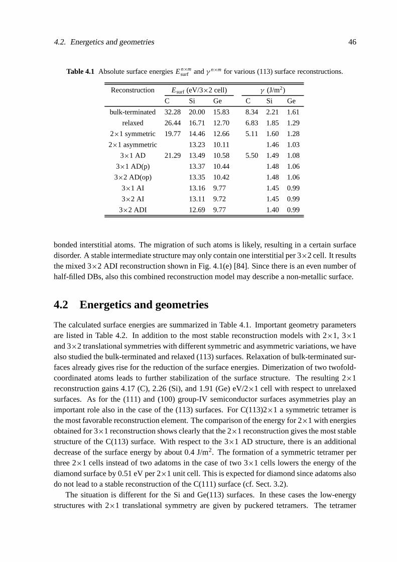
4.2. Energetics and geometries 46
Table 4.1 Absolute surface energies E n×msurf and γ n×m for various (113) surface reconstructions.
Reconstruction Esurf (eV/3×2 cell) γ (J/m2)
C Si Ge C Si Ge
bulk-terminated 32.28 20.00 15.83 8.34 2.21 1.61
relaxed 26.44 16.71 12.70 6.83 1.85 1.29
2×1 symmetric 19.77 14.46 12.66 5.11 1.60 1.28
2×1 asymmetric 13.23 10.11 1.46 1.03
3×1 AD 21.29 13.49 10.58 5.50 1.49 1.08
3×1 AD(p) 13.37 10.44 1.48 1.06
3×2 AD(op) 13.35 10.42 1.48 1.06
3×1 AI 13.16 9.77 1.45 0.99
3×2 AI 13.11 9.72 1.45 0.99
3×2 ADI 12.69 9.77 1.40 0.99
bonded interstitial atoms. The migration of such atoms is likely, resulting in a certain surfacedisorder. A stable intermediate structure may only contain one interstitial per 3×2 cell. It resultsthe mixed 3×2 ADI reconstruction shown in Fig. 4.1(e) [84]. Since there is an even number ofhalf-filled DBs, also this combined reconstruction model may describe a non-metallic surface.
4.2 Energetics and geometries
The calculated surface energies are summarized in Table 4.1. Important geometry parametersare listed in Table 4.2. In addition to the most stable reconstruction models with 2×1, 3×1and 3×2 translational symmetries with different symmetric and asymmetric variations, we havealso studied the bulk-terminated and relaxed (113) surfaces. Relaxation of bulk-terminated sur-faces already gives rise for the reduction of the surface energies. Dimerization of two twofold-coordinated atoms leads to further stabilization of the surface structure. The resulting 2×1reconstruction gains 4.17 (C), 2.26 (Si), and 1.91 (Ge) eV/2×1 cell with respect to unrelaxedsurfaces. As for the (111) and (100) group-IV semiconductor surfaces asymmetries play animportant role also in the case of the (113) surfaces. For C(113)2×1 a symmetric tetramer isthe most favorable reconstruction element. The comparison of the energy for 2×1 with energiesobtained for 3×1 reconstruction shows clearly that the 2×1 reconstruction gives the most stablestructure of the C(113) surface. With respect to the 3×1 AD structure, there is an additionaldecrease of the surface energy by about 0.4 J/m2. The formation of a symmetric tetramer perthree 2×1 cells instead of two adatoms in the case of two 3×1 cells lowers the energy of thediamond surface by 0.51 eV per 2×1 unit cell. This is expected for diamond since adatoms alsodo not lead to a stable reconstruction of the C(111) surface (cf. Sect. 3.2).
The situation is different for the Si and Ge(113) surfaces. In these cases the low-energystructures with 2×1 translational symmetry are given by puckered tetramers. The tetramer
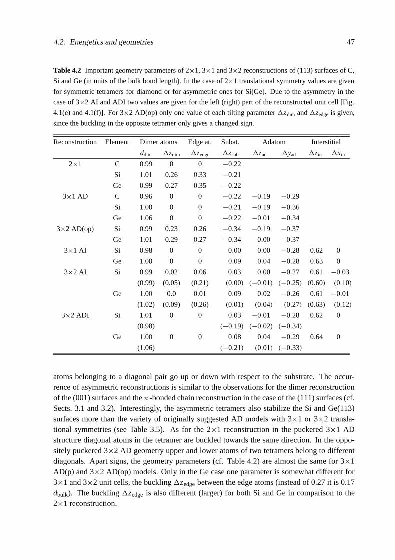
4.2. Energetics and geometries 47
Table 4.2 Important geometry parameters of 2×1, 3×1 and 3×2 reconstructions of (113) surfaces of C,
Si and Ge (in units of the bulk bond length). In the case of 2×1 translational symmetry values are given
for symmetric tetramers for diamond or for asymmetric ones for Si(Ge). Due to the asymmetry in the
case of 3×2 AI and ADI two values are given for the left (right) part of the reconstructed unit cell [Fig.
4.1(e) and 4.1(f)]. For 3×2 AD(op) only one value of each tilting parameter 1z dim and 1zedge is given,
since the buckling in the opposite tetramer only gives a changed sign.
Reconstruction Element Dimer atoms Edge at. Subat. Adatom Interstitial
ddim 1zdim 1zedge 1zsub 1zad 1yad 1zin 1xin
2×1 C 0.99 0 0 −0.22
Si 1.01 0.26 0.33 −0.21
Ge 0.99 0.27 0.35 −0.22
3×1 AD C 0.96 0 0 −0.22 −0.19 −0.29
Si 1.00 0 0 −0.21 −0.19 −0.36
Ge 1.06 0 0 −0.22 −0.01 −0.34
3×2 AD(op) Si 0.99 0.23 0.26 −0.34 −0.19 −0.37
Ge 1.01 0.29 0.27 −0.34 0.00 −0.37
3×1 AI Si 0.98 0 0 0.00 0.00 −0.28 0.62 0
Ge 1.00 0 0 0.09 0.04 −0.28 0.63 0
3×2 AI Si 0.99 0.02 0.06 0.03 0.00 −0.27 0.61 −0.03
(0.99) (0.05) (0.21) (0.00) (−0.01) (−0.25) (0.60) (0.10)
Ge 1.00 0.0 0.01 0.09 0.02 −0.26 0.61 −0.01
(1.02) (0.09) (0.26) (0.01) (0.04) (0.27) (0.63) (0.12)
3×2 ADI Si 1.01 0 0 0.03 −0.01 −0.28 0.62 0
(0.98) (−0.19) (−0.02) (−0.34)
Ge 1.00 0 0 0.08 0.04 −0.29 0.64 0
(1.06) (−0.21) (0.01) (−0.33)
atoms belonging to a diagonal pair go up or down with respect to the substrate. The occur-rence of asymmetric reconstructions is similar to the observations for the dimer reconstructionof the (001) surfaces and the π -bonded chain reconstruction in the case of the (111) surfaces (cf.Sects. 3.1 and 3.2). Interestingly, the asymmetric tetramers also stabilize the Si and Ge(113)surfaces more than the variety of originally suggested AD models with 3×1 or 3×2 transla-tional symmetries (see Table 3.5). As for the 2×1 reconstruction in the puckered 3×1 ADstructure diagonal atoms in the tetramer are buckled towards the same direction. In the oppo-sitely puckered 3×2 AD geometry upper and lower atoms of two tetramers belong to differentdiagonals. Apart signs, the geometry parameters (cf. Table 4.2) are almost the same for 3×1AD(p) and 3×2 AD(op) models. Only in the Ge case one parameter is somewhat different for3×1 and 3×2 unit cells, the buckling 1zedge between the edge atoms (instead of 0.27 it is 0.17dbulk). The buckling 1zedge is also different (larger) for both Si and Ge in comparison to the2×1 reconstruction.

4.2. Energetics and geometries 48
Indeed, puckering reduces the surface energy, but only within AD models. For silicon wecalculate an energy gain of 0.12 eV per 3×2 unit cell for the 3×1 AD(p) reconstruction. Thepuckered structure with 3×1 translational symmetry is only slightly higher in energy by 0.02eV compared with the 3×2 AD(op) reconstruction. Similar energy gains are obtained for ger-manium (cf. Table 4.1). The 3×1 puckered model lowers the surface energy by 0.14 eV forGe. The opposite puckering further lowers the surface energy by 0.02 eV, a value of the orderof the thermal energy at room temperature. Consequently, a flipping of the tetramers shouldbe already possible at room temperature. A phase transition between 3×1 and 3×2 structuresmay be easily imaginable in the framework of the AD model as suggested in the literature forSi [101, 106]. The small energy differences also suggest the local coexistence of phases withdifferent translational symmetries as observed in the Ge case [95, 99, 108].
The introduction of self-interstitials on Si and Ge(113) surfaces reduces the energy furtherin agreement with previous calculations [84, 108]. However, there is a sensitive balance ofdifferent energy contributions. For Si(113), the 3×2 ADI reconstruction [Fig. 4.1(f)] with onlyone interstitial atom per 3×2 unit cell gives the lowest-energy structure. The 3×1 and 3×2 AIstructures with more interstitials per unit area are less stable. With respect to the optimized 3×2AD(op) structure (Table 4.2), the adsorption of an interstitial atom gains energy of about 0.7eV within the 3×2 ADI model. Due to the repulsive interaction of the interstitials on the shortdistances this value is reduced to 0.2 eV per interstitial for AI geometries. For Ge the energiesof the 3×1 AI and 3×1 ADI models are equal. The novel asymmetric 3×2 AI model gives riseto the lowest energy structure. There is an energetical ordering 3×1 AI/3×2 ADI and 3×2 AI,which is different from that observed for Si(113). The repulsive interaction of the interstitials ismuch weaker in the germanium case. The energy gain of 0.6 eV by adding an Ge interstitial ina 3×2 ADI structure is reduced to 0.3 eV per interstitial in the AI cases.
Within the interstitial models pronounced asymmetries are found only for the 3×2 AI re-construction (cf. Table 4.1). There is a general tendency to break the symmetry between thetwo pentamers. Such asymmetries have been observed in STM images for the seemingly 3×1reconstruction [108]. The unit cell of the 3×2 AI reconstruction is doubled by opposite buck-ling of the two pentamers, where the interstitial atoms can also change their central positions.Such a staggered arrangement of buckled pentamers lowers the total energy by about 50 meVfor Si and Ge and results in the 3×2 AI model. Here we present the most favorable asymmetrieswhich have been found. Other asymmetries, e.g. an average relative vertical displacement ofthe two pentamers within the 3×2 AI model, also lower the total energy. One observes differentlocal minima on the total-energy surface with practically the same surface energies. The bandstructures of the two geometries are nearly identical. Particularly for Si the asymmetry opens agap. The removal of one interstitial, i.e., the transition to the 3×2 ADI structure, further lowersthe energy in the Si case but not for Ge(113). For the 3×2 ADI reconstruction an additionalasymmetry is not favorable for both materials.
The small energetical differences between ADI and AI models may explain the observedtemperature-induced order-disorder phase transitions [91, 94–96, 99, 104, 105, 108]. The lowtemperature of about 120 K for Ge and the high temperature of about 800 K for Si seem tobe correlated with the differences in the corresponding surface energies between AI and ADI

4.3. Band structures and electronic states 49
structures. According to the small binding energy of the second interstitial, surface diffusionmust play an important role, in particular the migration of the interstitial atoms [108]. Such amigration at a certain temperature may be accompanied by a certain amount of surface disorderand, hence, explains the coexistence of 3×1 and 3×2 reconstructed domains on a given (113)surface [94, 97, 99, 101, 108]. In the Si(113) case the observation of 3×1 instead of 3×2 seemsto be also dependent on the density of the surface defects and the bulk doping [89, 93].
The energetical ordering of the reconstruction models in Table 4.1 is the same as in other abinitio calculations [84, 92, 106, 108], apart that the 2×1 and asymmetric 3×2 AI structures havenot been studied. In particular, interstitial models give the lowest-energy structures. We agreethat 3×2 ADI is the lowest-energy structure for Si(113) and with nearly the same energies forall interstitial reconstructions of Ge(113). However, the calculated absolute surface energies perunit area, γ , in Table 4.1 are slightly smaller than those computed by other authors [84, 92, 108].This holds for both Si and Ge(113).
4.3 Band structures and electronic states
In order to understand the driving forces of the reconstructions and the electronic structures ofthe (113) surfaces for diamond, Si and Ge, band structures for all important models have beencalculated. The corresponding resulting band structures of (113)2×1 surfaces are plotted inFig. 4.2 versus the variation of the k points between high-symmetry points in the surface BZ ofthe oblique lattice (see Sect. 2.9). The C(113)2×1 surface with tetramers shows a significantinsulating behavior. Two neighbored empty surface bands in the upper part of the projectedfundamental gap are well separated from the two completely filled surface bands somewhatbelow the VBM of the bulk band structure. The indirect energy gap is related to a transitionfrom the 0P line to the J point and amounts to 2.1 eV within the DFT-LDA, i.e., half the valueof the bulk gap. Surprisingly, already the symmetric tetramers give rise to the opening of asurface gap for Si(113)2×1, though the gap is small with 0.4 eV. This is not the case for thesymmetric-dimer reconstruction of the Si(001)2×1 surface (cf. Sect. 3.1) for reasons which willbe seen discussing the nature of the electronic states below. A gap opening does not occur forsymmetric tetramers on Ge(113)2×1. However, the prediction of the surface band structure isdifficult due to the remarkable band-gap underestimate within the DFT-LDA already for bulkGe. In any case, for Si and Ge there is a tendency to open the surface gap by puckering of thetetramers. The occupied bands, in particular for Ge, are shifted into the projected valence bandsand only an empty surface state band remains in the projected fundamental gap. However, dueto its strong dispersion the Ge(113)2×1 surface with asymmetric tetramers remains metallic.The low position and the strong dispersion of the lower surface band for Ge(113)2×1 is aconsequence of the bulk electronic structure. The bulk conduction-band states arising not farfrom the L point in the fcc BZ repel the surface band at J (which is in contrast empty forC and Si) towards lower energies even below the VBM. The general tendency of shifting thesurface bands and opening gaps between surface states with the asymmetry of the tetramers is

4.3. Band structures and electronic states 50
Figure 4.2 Electronic band structures of C, Si and Ge(113)2×1 surfaces. The band structures
in the upper panels are calculated for symmetric tetramers, while the lower ones represent asym-metric tetramers.
in agreement with similar findings for the (111) and (001) low-index surfaces of Si and Ge (cf.Sects. 3.1 and 3.2).
The physical/chemical origin of the surface bands is indicated in Figs. 4.3 and 4.4. Thesquares of the wave functions are plotted for the two lowest empty surface bands and the twohighest occupied surface bands for symmetric tetramers [C(113)2×1, Fig. 4.3] and asymmetrictetramers [Si(113)2×1, Fig. 4.4]. The character of the four surface bands within the fundamen-tal gap is dominated by the six dangling-bond orbitals situated at the four tetramer atoms (oneon each (111)-like atom (or edge atom ) and two on each (001)-like atom (or dimer atom) ofthe tetramer) as indicated in Fig. 4.1(a) for the surface atoms in bulk positions. Their linearcombinations form the surface-state wave functions. Even for the symmetric case of diamond,the two sp3 orbitals of each (001)-like atom cannot be dehybridized in such a way forming σand π orbitals with respect to the directions [113] and [110] as in the classical dimer pictureof (001) surfaces [48]. In contrast to (111) and (001) surfaces with exact π and σ orbitals, sixsp3-like dangling bonds have to be discussed to explain the electronic structure of the tetramer.
As a consequence, for diamond only one bond along the [110] direction is nearly formedby two sp3-like orbitals located at (001)-like atoms. The remaining dangling bonds stronglyinteract with the dangling bonds of the neighbored (111)-like edge atoms of the tetramer. Inthe case of C(113)2×1 the distance of the two (001)-like atoms in the tetramer amounts 99%(Table 4.1) of a bulk bond length dbulk. This is in contrast to a dimer bond length 0.90 dbulk

4.3. Band structures and electronic states 51
Figure 4.3 Wave-function squares of the lowest unoccupied c2 (a), c1 (b) and highest occupied
v1 (c), v2 (d) surface bands at P for the C(113)2×1 reconstruction. In (a) and (c) cases sideviews are additionally plotted in the left panels in order to show the contributions below thetetramer plane.
calculated for C(001)2×1 (Table 3.2). Interestingly the two bond lengths between edge anddimer atoms in the tetramer are reduced to 0.89 dbulk. The reason is a true dimer-like behaviorof two such atoms. Already in the bulk case a σ bond exists. An additional bond is formed bythe two dangling hybrids of the edge and dimer atoms. No asymmetry occurs in the tetramerbecause of the strong bonding between the carbon atoms which takes place due to the lack of pand d electrons in the atomic core. The tetramers nearly show a mirror symmetry along [332].They are almost planar. Only a small difference of 0.22 A remains between dimer and edgeatoms along the z direction as an artifact of the atomic positions in the bulk-terminated surface.As a consequence of the weak bonding of the so-called dimer atoms, the occupied tetramerstates in Fig. 4.3(c) and Fig. 4.3(d) are governed by antibonding (bonding) combinations ofdangling orbitals at dimer atoms and bonding (antibonding) combinations of dangling orbitalslocated at edge and dimer atoms. However, there are also contributions from the orbitals aroundthe central atom below the tetramer. The unoccupied states are dominated by antibonding linearcombinations of dangling bonds located at the dimer and edge atoms.
Because of the most favorable asymmetric (puckered) tetramer structures the surface statesare completely changed for the Si and Ge(113)2×1 surfaces. A tetramer does not anymoreform a planar structure. Starting from the left edge atom, approaching the two so-called dimeratoms, and going around to the second edge atom one finds the following variations 1z in thevertical positions, 0, 0.91, 0.29, and 0.77 A (0, 0.98, 0.33, and 0.86 A) for Si (Ge). The dimerbond length between two (001)-like atoms amounts to 1.01 (0.99) dbulk, whereas the lengthsbetween (111) and (001) atoms are 0.97 (0.95) dbulk for Si(113) [Ge(113)]. For Si(113)2×1 thewave-function squares of the surface states are shown in Fig. 4.4. Because of their similaritythose for Ge are not plotted. The consequence of the asymmetry of the tetramers is obvious.

4.3. Band structures and electronic states 52
Figure 4.4 Wave-function squares of the lowest unoccupied c2 (a), c1 (c) and highest occupied
v1 (c), v2 (d) surface bands at P for the asymmetric tetramer reconstruction of the Si(113) sur-face. The band v2 (d) occurs in the projected band structure of the valence bands and, hence, isnot indicated in Fig. 4.2. In (a) and (c) side views are also plotted in the left panels.
The different surface states at the P point in the BZ are mainly due to orbitals located at onetetramer atom. The two lowest unoccupied states are localized at the two down atoms forminga diagonal of the tetramer. The two considered occupied states are mainly localized at the twoupper atoms. Energetically the lowest one lies already in the projected bulk band structure(cf. Fig. 4.2). The situation shows similarities to the asymmetric-dimer reconstruction of theSi(001)2×1 surface. The outgoing atoms become a more s-like dangling orbital, whereas theatoms displaced towards the substrate show a more pz-like character of the dangling orbital.Electron transfer from the more pz-like orbitals into the more s-like orbitals is expected tolower the total energy of the system.
Electronic band structures of different 3×1 and 3×2 surface reconstuctions for Si andGe(113) surfaces are plotted in Fig. 4.5. In principle, a similar behavior is observed for Siand Ge. Similar to the 2×1 case, modifications are related to differences in the bulk band struc-tures. For Ge a small direct gap at 0 and a conduction-band minimum (CBM) at L instead of at0.85 0X are found. The minima at L points are responsible for the deep projected conductionbands at the K point of the surface BZ. Moreover, the weaker bonding in Ge plays a role. The3×1 AD model [Fig. 4.5(a)] clearly gives a metallic behavior of the (113) surfaces in agree-ment with the three half-filled (without buckling) DBs. DB-related bands overlap partially withbulk states near the VBM. The Fermi level at an energy near the VBM crosses these bands.A similar behavior is observed for the lowest-energy AD structure of the C(113)3×1 surface.The metallic character remains true for the puckered AD, but surprisingly also for the oppo-sitely puckered 3×2 AD structures [Fig. 4.5(b)]. The DBs at the adatoms still weakly interactand the splitting of the two bands due to asymmetric displacements and DB interaction is toosmall. This is in contrast to the band structure obtained within a TB approximation by Wang
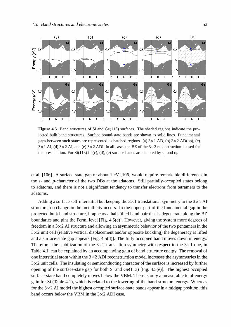
4.3. Band structures and electronic states 53
Figure 4.5 Band structures of Si and Ge(113) surfaces. The shaded regions indicate the pro-
jected bulk band structures. Surface bound-state bands are shown as solid lines. Fundamentalgaps between such states are represented as hatched regions. (a) 3×1 AD, (b) 3×2 AD(op), (c)
3×1 AI, (d) 3×2 AI, and (e) 3×2 ADI. In all cases the BZ of the 3×2 reconstruction is used forthe presentation. For Si(113) in (c), (d), (e) surface bands are denoted by v i and ci .
et al. [106]. A surface-state gap of about 1 eV [106] would require remarkable differences inthe s- and p-character of the two DBs at the adatoms. Still partially-occupied states belongto adatoms, and there is not a significant tendency to transfer electrons from tetramers to theadatoms.
Adding a surface self-interstitial but keeping the 3×1 translational symmetry in the 3×1 AIstructure, no change in the metallicity occurs. In the upper part of the fundamental gap in theprojected bulk band structure, it appears a half-filled band pair that is degenerate along the BZboundaries and pins the Fermi level [Fig. 4.5(c)]. However, giving the system more degrees offreedom in a 3×2 AI structure and allowing an asymmetric behavior of the two pentamers in the3×2 unit cell (relative vertical displacement and/or opposite buckling) the degeneracy is liftedand a surface-state gap appears [Fig. 4.5(d)]. The fully occupied band moves down in energy.Therefore, the stabilization of the 3×2 translation symmetry with respect to the 3×1 one, inTable 4.1, can be explained by an accompanying gain of band-structure energy. The removal ofone interstitial atom within the 3×2 ADI reconstruction model increases the asymmetries in the3×2 unit cells. The insulating or semiconducting character of the surface is increased by furtheropening of the surface-state gap for both Si and Ge(113) [Fig. 4.5(e)]. The highest occupiedsurface-state band completely moves below the VBM. There is only a measurable total-energygain for Si (Table 4.1), which is related to the lowering of the band-structure energy. Whereasfor the 3×2 AI model the highest occupied surface-state bands appear in a midgap position, thisband occurs below the VBM in the 3×2 ADI case.

4.3. Band structures and electronic states 54
Figure 4.6 Wave-function squares of the highest occupied and lowest unoccupied surface bandsat K for the Si(113) surface within the 3×1 and 3×2 AI reconstructions. (a) two fully occupied
states v2/3, (b) half-occupied v1/c1 and (c) lowest conduction states c2/3 of 3×1 AI model. (d)and (e) highest occupied (v1) and lowest unoccupied (c1) bands of 3×2 AI surface reconstruc-tion. Corresponding electronic structures with band indication are shown in Figs. 4.5(c) and
4.5(d).
The findings of a semiconducting behavior of Si(113)3×2 surfaces are in agreement withPhotoemission Spectroscopy (PES), Angle-Resolved Photoelectron Spectroscopy (ARPES),and STM studies. PES of Ranke and Xing [178] gave the Fermi level in a midgap positionof about 0.5 eV above the VBM. This energy region was shown to be free of occupied surfacestates as demonstrated in Fig. 4.5(e) for the 3×2 ADI structure. At normal emission and athigher emission angles ARPES [102] found two surface bands separated by 0.4 eV below theVBM in a k-vector direction parallel to [110]. Along J K but also along J ′0 (but within thebulk states), we also observe such a pair of surface states in Fig. 4.5(e). Their splitting is smallerthan the measured value. One reason may be the neglect of the quasiparticle corrections. Differ-ential tunneling conductance spectra taken at various sites in the 3×2 unit cell on topographicimages for both positive and negative voltages also indicate the existence of surface states forSi(113)3×2 [89]. A broad occupied surface-state feature is observed 0.8 eV below the Fermilevel in agreement with PES [179] or 1 eV in Ref. [105]. The gap of about 1.2 eV is almost freeof surface states in agreement with the calculations for 3×2 ADI.
As in the case of 2×1 reconstructions the interpretation and identification of the surfacebands is more complicated for the Ge(113) surface. However, away from the 0 point the situa-tion becomes clear. The slab band structures show a small gap for both the 3×2 AI and the 3×2ADI models [Figs. 4.5(d) and 4.5(e)]. The resulting semiconducting behavior is also confirmed

4.3. Band structures and electronic states 55
(a)
(d)(c)
(b)
Figure 4.7 Wave-function squares of the high-est occupied (v2, v1) [(a) and (b)] and lowestunoccupied (c1, c2) [(c) and (d)] surface bands
at K for the Si(113) surface within the 3×2ADI reconstruction [see Fig. 4.5(e)].
by PES measurements which found the VBM to be 0.22 eV below the Fermi level and thisenergy region free of surface states [180].
In order to figure out the true nature of the surface-state bands in the fundamental gap ofthe projected bulk band structure, the wave functions of the highest occupied (v1, v2, v3) andlowest unoccupied (c3, c2, c1) surface bands are plotted in Figs. 4.6 and 4.7. 3×1 and 3×2interstitial reconstructions of the Si(113) surface are studied at the K point in the BZ of the3×2 lattice. At least for Si(113) the states at K are well separated from the bulk states and,hence, show a remarkable localization. In the Ge case there is an energetical overlap of theempty surface bands with the bulk conduction bands at K . Figure 4.6(a) shows for the 3×1 AImodel that the two degenerate surface bands v2/3 below the VBM are localized at the adatomsand that each DB of an adatom is completely filled. This filling indicates the main effect of thepresence of the interstitials. The DBs at the adatoms are filled and, consequently, adatoms moveup (see Table 4.2). The wave functions of the half-filled bands v1/c1 in the upper part of thefundamental gap [Fig. 4.5(c)] are localized at edge atoms and the subatoms which are originallysituated in the third atomic layer. Originally the edge atoms possess half-filled dangling bonds.However, the occurrence of a probability to find electrons at the third-layer atom is somewhatunexpected. That means, this atom is not anymore completely fourfold-coordinated. Rather,because of the presence of the interstitial one bond is weakened, allowing the atom in the fourthatomic layer to form a bond with the interstitial atom. Higher states which appear in the gap(c1/2) are localized on the dimer atoms [Fig. 4.6(c)].
The asymmetry in the two pentamers of the 3×2 AI reconstruction governs the gap opening[Fig. 4.5(d)]. The atoms of the pentamer which is closer to the substrate tend to have more p-like DB states. An electron transfer happens from the electronic states localized at this pentamerinto the more s-like states at the pentamer that is somewhat displaced away from the bulk. Thedifference of buckling in the pentamers also plays a role (cf. Table 4.2). Nevertheless, the

4.4. STM images 56
atoms with higher positions are more filled and contribute to the v1 [Fig. 4.6(d)]. The lowestconduction-band states c1 are localized at the second pentamer [Fig. 4.6(e)]. The higher statesshould be observable at the lower parts of the pentamers (not shown).
For the 3×2 ADI model the filled and empty surface states v1,v2 and c1,c2 are shown in Fig.4.7. The occupied states in Fig. 4.7(a) and 4.7(b) are again localized at adatoms. The emptystates belong to the pentamer [Fig. 4.7(c) and 4.7(d)]. Surprisingly, the wave functions aroundthe subsurface interstitial do not contribute to the surface-state bands in the gap. For that reason,they are not visible in STM measurements for not too large voltages [84, 92].
4.4 STM images
The different contributions of the empty and filled electronic states localized at the pentamers,tetramers and the two rebonded adatoms in a certain 3×2 interstitial surface reconstruction willalso dominate the STM images. This is demonstrated in Fig. 4.8 for voltages corresponding toenergy intervals of 2 eV below or above the theoretical Fermi level within the fundamental gapin DFT-LDA quality. Results are for Si(113), the 3×2 AI structure in Fig. 4.8(a) and the 3×2ADI reconstruction in Fig. 4.8(b). Those for Ge(113) are very similar. The main differences aredue to the strength of the buckling within the 3×2 AI reconstruction.
The resulting STM images are in accordance with the discussion of the orbital characterof the gap states in Fig. 4.6 and 4.7. Figure 4.8(a) for the 3×2 AI model clearly shows thatthe filled-state images are dominated by the wave functions localized at the adatoms. The twopentamers are less visible. However, the right part of the upper pentamer shows brighter spots.They are related to the pronounced asymmetry of the two pentamers. The empty-state imagesshow an opposite behavior. The pentamers are clearly visible whereas only weak contributionsare associated with the adatoms. The asymmetry in the upper pentamer is indicated by some-what smeared-out spots. The interstitial atoms are not visible. In principle such nonsymmetricpentamers are observed experimentally for seemingly 3×1 areas of the Ge(113) surface [108].Although the asymmetry can be seen there, it is difficult to distinguish whether the 3×1 or3×2 AI reconstruction appears on the surface, at least in empty-state images. Consequently it isalso difficult to distinguish between 3×1 or 3×2 translational symmetries using a local methodsuch as STM.
The observation of pentamer-like structures in empty-state images [89, 93, 107] shouldbe taken as an indication for an interstitial. This is clearly shown in Fig. 4.8(b) for the 3×2ADI model by the differences between spot arrangements related to pentamers or tetramers.The dimer atoms in the upper-right feature appear in both empty-state and filled-state images,whereas the pentamer is more (empty-state) or less (filled-state) visible. More in detail, thefilled-state image is dominated by electronic states localized at the adatoms, as in the case withtwo interstitials, i.e., the 3×2 AI (or 3×1 AI) reconstruction. For Si(113)3×2 [93], as wellas Ge(113)3×2 [108], such filled-state images have indeed been observed. The adatoms getelectrons from the pentamers to fill their partially occupied states. In the empty-state image[Fig. 4.8(b), right] the adatoms are not seen. The pentamer can be well identified, while the
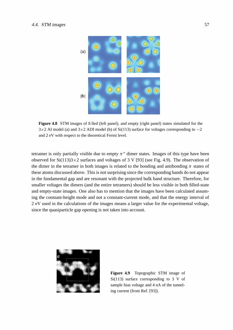
4.4. STM images 57
Figure 4.8 STM images of filled (left panel), and empty (right panel) states simulated for the3×2 AI model (a) and 3×2 ADI model (b) of Si(113) surface for voltages corresponding to −2
and 2 eV with respect to the theoretical Fermi level.
tetramer is only partially visible due to empty π ∗ dimer states. Images of this type have beenobserved for Si(113)3×2 surfaces and voltages of 3 V [93] (see Fig. 4.9). The observation ofthe dimer in the tetramer in both images is related to the bonding and antibonding π states ofthese atoms discussed above. This is not surprising since the corresponding bands do not appearin the fundamental gap and are resonant with the projected bulk band structure. Therefore, forsmaller voltages the dimers (and the entire tetramers) should be less visible in both filled-stateand empty-state images. One also has to mention that the images have been calculated assum-ing the constant-height mode and not a constant-current mode, and that the energy interval of2 eV used in the calculations of the images means a larger value for the experimental voltage,since the quasiparticle gap opening is not taken into account.
Figure 4.9 Topographic STM image of
Si(113) surface corresponding to 3 V ofsample bias voltage and 4 nA of the tunnel-ing current (from Ref. [93]).

Chapter 5
Low-index surfaces II − (110)
5.1 Translational symmetry of (110)16×2 surfaces
Clean Si(110) [at certain conditions [80, 81] also Ge(110)] surfaces exhibit 16×2 reconstruc-tions. It was found by using High-Energy Electron Diffraction (RHEED) or LEED in the cor-responding patterns, superstructure spots divide the two fundamental spots into 16. Using thebasis vectors a = (−1, 1, 0)a0/2 and b = (0, 0, 1)a0 (a0 - bulk lattice constant) of the two-dimensional rectangular Bravais lattice with 1×1 unit cells (see Fig. 5.1), the 16×2 structurehas to be described as
√171×
√6 − R(32.73◦, 35.26◦) surface within the Wood notation or as
(
11 −52 2
)
within matrix notation [44]. The unit cell of the resulting oblique lattice with the primitivebasis vectors a = (−11, 11,−10)a0/2 and b = (−1, 1, 2)a0 is also shown in Fig. 5.1. Thereis a deviation of 2.5◦ of the first vector a from the vector (−1, 1,−1)16a0/3 giving rise to arectangular unit cell. Nevertheless, we still use the denotation “16×2 reconstruction”, since theunit cell area actually amounts to 32 unit cell areas of the 1×1 surface.
5.2 Bond-rotation/bond-contraction relaxation mechanism
A 1×1 unit cell of (110) surfaces consists of two atoms with one dangling bond at each atomconnected by two in-plane bonds, introducing in this way a zigzag chain (cf. Fig. 5.2). Inthe case of zinc-blende crystals where (110) is the cleavage face this bulk-terminated (1×1)translational symmetry is preserved. After the relaxation surface atoms possess asymmetricpositions, one atom goes up while the other one moves down, thereby introducing a buckledchain. The relaxation is characterized by a so-called bond-rotation or bond-contraction modelin dependence on strength and ionicity of the bonds [181]. These chains are characterized by abond length dchain and a buckling 1z of the two atoms in a 1×1 unit cell. Basically the sametype of relaxation may occur in the case of the group-IV elements. Table 5.1 shows that inthe diamond-structure case the Si and Ge(110)1×1 surfaces are clearly described by the bond-rotation mechanism. The bulk bond lengths are conserved but substantial chain bucklings are
58

5.2. Bond-rotation/bond-contraction relaxation mechanism 59
Figure 5.1 Top view of a bulk-terminated (110) surface with 1×1 (dotted line) and possible16×2 (solid line) unit cells. Dots (circles) represents first(second)-layer atoms. The directionsof the primitive basis vectors of the 1×1 and 16×2 lattices are indicated. The deviation from the
rectangular lattice is demonstrated by the small difference in the directions [11 11 10] and [111].
predicted. Diamond(110)1×1 exhibits the opposite behavior, i.e., it is characterized by a bond-contraction relaxation mechanism. There is no buckling but a remarkable shortening of thechain bonds. In any case relaxation gives rise to an energy gain (cf. Table 5.2)
Figure 5.3 presents the bands of the clean relaxed (110)1×1 surfaces together with theprojected bulk band structures. The two dangling bonds per surface unit cell lead to two bands,which are situated within the projected bulk fundamental gap. In the diamond case the twodangling bonds remain equivalent. Consequently the two bands degenerate along the M X line,i.e., perpendicular to the surface chain orientation. The bands split along the other BZ boundaryM X ′. Along the 0X and 0X ′ directions the surface bands exhibit a remarkable dispersion.
Figure 5.2 Perspective view of zigzag chain on the (110) surfaces.
5.2. Bond-rotation/bond-contraction relaxation mechanism 60
Table 5.1 Geometry parameters of (110)1×1 reconstruction. Lengths are given inunits of the bulk bond length. The chain buckling (rotation) is also characterized by
the tilt angle ω (in degrees).
Geometry parameter Diamond Silicon Germanium
ω 0.0 19.6 19.8
1z 0.00 0.33 0.34
dchain 0.93 0.99 1.00
Table 5.2 Absolute surface energies E n×msurf and γ n×m for various (110) surface reconstructions.
Reconstruction Esurf (eV/1×1 cell) γ (J/m2)
C Si Ge C Si Ge
bulk-terminated 4.12 2.63 2.13 7.48 2.04 1.52
1×1-relaxed 3.26 2.19 1.66 5.93 1.70 1.19
1×2-chain 2.18 1.64 1.69 1.17
16×2-chain 2.19 1.70
16×2-chains on terraces 2.17 1.69
2×1-adatom 2.14 1.59 1.66 1.14
c(2×2)-adatom 2.26 1.84 1.76 1.32
3×1-adatom 2.09 1.72 1.63 1.23
3×2-adatom 2.23 1.81 1.72 1.29
16×2-adatom-1 2.24 1.74
16×2-adatom-2 2.16 1.68
6×2-adclusters − − − −16×2-hexagon 2.45 1.90
3×2 ATI 2.09 1.61 1.63 1.15
16×2 TI 2.24 1.74
16×2 ATI 2.14 1.66
Consequently the C(110)1×1 surface is metallic. Along the row C→Si→Ge the chemicaltrend is similar to that in the (111)2×1 case (cf. Sect. 3.2). The chain buckling (cf. Table5.1) lifts the degeneracy of the two bands along M X . However, in the Si case the effect isnot strong enough. The Si(110)2×1 surface becomes semimetallic. For Ge(110)2×1 a truesurface-state gap is opened along the M X line. On the other hand, the bands are shifted towardsthe occupied bulk bands and the uppermost band exhibits a strong dispersion as a consequenceof the interchain interaction. It also results a semimetallic surface electronic structure.
For Si and Ge(110) surfaces a bond-rotation or bond-contraction relaxation mechanism isnot the most favorable one assuming not too differing translational symmetries. A more stable

5.2. Bond-rotation/bond-contraction relaxation mechanism 61
reconstruction with parallel chains buckled in opposite directions is presented in Fig. 5.4(a).This 1×2 reconstruction is energetically more favorable than the relaxed 1×1 one for bothmaterials. The energy gains due to the various buckling contributions of the chains are only ofthe order of 10 meV for Si and slightly larger for Ge (about 20 meV) (see Table 5.2). The surfacestabilization in a 1×2 reconstruction by chains in anti-phase agrees with previous theoreticalfindings [85, 86]. The values of the buckling amplitudes are 0.75 and 0.80 A for Si and Ge,respectively. The preference of the 1×2 reconstruction can be related to a gain of band-structureenergy. The corresponding electronic band structures are plotted in Fig. 5.5(a). In contrast tothe findings for the relaxed 1×1 surface (cf. Fig. 5.3), the alternate buckling of parallel chainsin the 1×2 reconstruction opens a fundamental band gap between surface bands. For Si a smallgap is observed along the J ′K direction. The interchain interaction is effectively reduced.The band folding together with the repulsion of bands decrease the band dispersion in chaindirection. For Ge the band structure in Fig. 5.3(a) still indicates a metallic behavior. However,the interpretation of the Ge electronic states is more difficult because of the underestimation ofthe band gaps within the DFT-LDA already for bulk, as discussed above. The dispersion of thesurface bands in Fig. 5.3 is not too large, and the bands mostly overlap near the 0 point. Theremay be a chance to open a gap using the quasiparticle approach. This also holds for other Gesurface reconstructions discussed below. In contrast to the Ge case the Si(110)1×2 surface withoppositely buckled parallel chains is semiconducting. The dispersion of the surface bands near0 is much weaker. For Si(110)1×2 the squares of the wave-functions at K are shown for thehighest occupied and lowest unoccupied states in Fig. 5.6. The principal behavior is similar tothe case of equally buckled chains in 1×1 cells. The states localized on upper atoms are fullyoccupied and behave as s-like orbitals, while those on lower atoms are empty and have pz-likecharacter. The surface states are similar for Ge (not shown).
Another 1×2 reconstruction may be related to a phase-shifted arrangement of π -bondeddimers [83], due to the rebonding of dangling bonds of neighboring first-layer atoms belongingto the same chain along the [110] direction (not shown). The total-energy optimization showedthat such dimer arrangements are not stable. During the atomic relaxation the starting dimerconfiguration is transformed back into a chain structure. The reason is that it is not favorable
Figure 5.3 Band structure of relaxed (110)1×1 surfaces.

5.2. Bond-rotation/bond-contraction relaxation mechanism 62
Figure 5.4 Side and top views of relaxed atomic positions of Si(110) surfaces (those for Ge aresimilar): (a) 1×2 chain buckled model, (b) 2×1 adatom model, (c) c(2×2) adatom model, (d)3×1 adatom model, (e) 3×2 adatom model, (f) 6×2 five-membered adatom model, and (g) 3×2
adatom-tetramer-interstitial model. Lateral unit cells are indicated by thin solid lines in the topviews.
to break a σ bond which already exists and to create a dimer with a π bond which is weaker.Consequently, it is not possible to cover Si and Ge(110) surfaces by neighboring dimers.
The next important point in the understanding of (110) surfaces, in particular of Si(110)16×2,is related to study of the step configuration observed by STM. First we have studied a Si(110)16×2reconstruction using the bond-rotation relaxation model where chains are buckled in one direc-tion like in nominal 1×1 cell. It gives an idea about the convergence of the total-energy andforce calculations using the 16×2 oblique Bravais lattice with primitive vectors a and b indi-cated in Fig. 5.1. The energy gain of 0.44 eV per 1×1 unit cell (cf. Table 5.2) is the same valueas computed using the 1×1 rectangular Bravais lattice with primitive vectors a and b.
A structure with two terraces and two steps in a 16×2 unit cell can be prepared by remov-ing one half of the first-layer atoms along the [112] direction. However, a simple relaxationof the atoms on both terraces as in the 1×1 case yields an energy gain smaller than the value0.44 eV/1×1 cell due to the presence of the steps. A more intelligent adaption of steps parallelto [112] and chains parallel to [110] is needed. One idea is presented in Fig. 5.7(a). It is based

5.2. Bond-rotation/bond-contraction relaxation mechanism 63
Figure 5.5 Band structures of Si and Ge(110) surfaces. (a) 1×2 with oppositely buckled chains,
(b) 2×1 adatom model, (c) 3×1 adatom model, and (d) 3×2 adatom-tetramer-interstitial model.The Brillouin zone of the 2×2 (3×2) structure is used to present the bands obtained for 1×2,
2×1 (3×1, 3×2) translational symmetry. The high-symmetry lines are scaled in such a way thatthe ordinate axis has the same extension, independent of the considered translational symmetry.
on the preference of the 1×2 chain reconstruction. As a result of the chain buckling in oppo-site directions different distances of the chains parallel to [001] occur on both terraces. Thesedistances ”up” and ”down” between chains with raised and lowered atoms are indicated in Fig.5.7(a). There are also lateral displacements of the chain atoms which nearly conserve the bondlengths (cf. Table 5.1). Buckled atoms allow two basically different bonding configurationsbetween chain atoms of the upper and lower terraces across a step. After the formation of thetrench each edge atom on the uppermost terrace possesses two dangling bonds. One of theseDBs may be rebonded with a DB of an atom from the lower terrace if their distance is not toolarge. According to Fig. 5.7(a) the lowered atom of a chain of the upper terrace is more preferedto continue a chain on the lower terrace. By means of the total-energy minimization we foundthat within such a step configuration indeed rebonding of each edge atom on the upper andlower terraces takes place. One has to mention that a similar step structure has been proposedto explain the stripes by pairs of pentagons [182]. In this model the rest atoms at the chains arealso correspondingly buckled [75].
The described step structure is energetically favorable. The surface energy of the systemwith oppositely buckled chains on the terraces and rebonded step atoms is lower in energy by 20meV/1×1 unit cell (cf. Table 5.2) compared with the surface without steps. This corresponds to
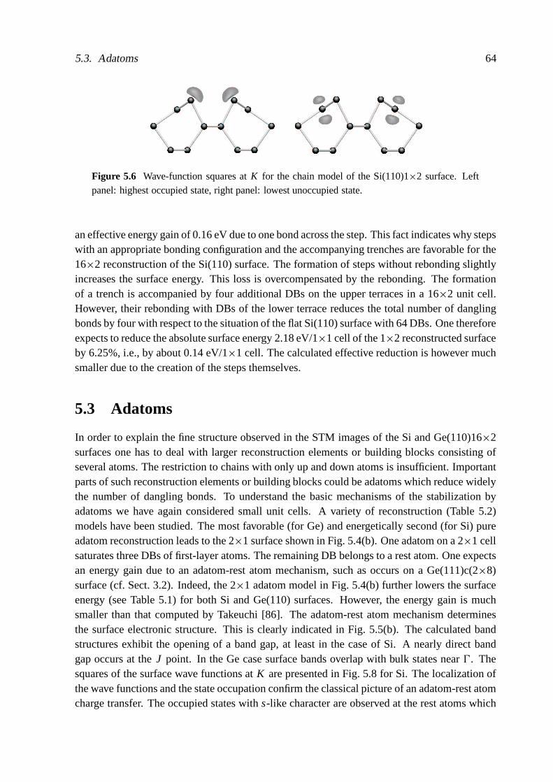
5.3. Adatoms 64
Figure 5.6 Wave-function squares at K for the chain model of the Si(110)1×2 surface. Leftpanel: highest occupied state, right panel: lowest unoccupied state.
an effective energy gain of 0.16 eV due to one bond across the step. This fact indicates why stepswith an appropriate bonding configuration and the accompanying trenches are favorable for the16×2 reconstruction of the Si(110) surface. The formation of steps without rebonding slightlyincreases the surface energy. This loss is overcompensated by the rebonding. The formationof a trench is accompanied by four additional DBs on the upper terraces in a 16×2 unit cell.However, their rebonding with DBs of the lower terrace reduces the total number of danglingbonds by four with respect to the situation of the flat Si(110) surface with 64 DBs. One thereforeexpects to reduce the absolute surface energy 2.18 eV/1×1 cell of the 1×2 reconstructed surfaceby 6.25%, i.e., by about 0.14 eV/1×1 cell. The calculated effective reduction is however muchsmaller due to the creation of the steps themselves.
5.3 Adatoms
In order to explain the fine structure observed in the STM images of the Si and Ge(110)16×2surfaces one has to deal with larger reconstruction elements or building blocks consisting ofseveral atoms. The restriction to chains with only up and down atoms is insufficient. Importantparts of such reconstruction elements or building blocks could be adatoms which reduce widelythe number of dangling bonds. To understand the basic mechanisms of the stabilization byadatoms we have again considered small unit cells. A variety of reconstruction (Table 5.2)models have been studied. The most favorable (for Ge) and energetically second (for Si) pureadatom reconstruction leads to the 2×1 surface shown in Fig. 5.4(b). One adatom on a 2×1 cellsaturates three DBs of first-layer atoms. The remaining DB belongs to a rest atom. One expectsan energy gain due to an adatom-rest atom mechanism, such as occurs on a Ge(111)c(2×8)surface (cf. Sect. 3.2). Indeed, the 2×1 adatom model in Fig. 5.4(b) further lowers the surfaceenergy (see Table 5.1) for both Si and Ge(110) surfaces. However, the energy gain is muchsmaller than that computed by Takeuchi [86]. The adatom-rest atom mechanism determinesthe surface electronic structure. This is clearly indicated in Fig. 5.5(b). The calculated bandstructures exhibit the opening of a band gap, at least in the case of Si. A nearly direct bandgap occurs at the J point. In the Ge case surface bands overlap with bulk states near 0. Thesquares of the surface wave functions at K are presented in Fig. 5.8 for Si. The localization ofthe wave functions and the state occupation confirm the classical picture of an adatom-rest atomcharge transfer. The occupied states with s-like character are observed at the rest atoms which
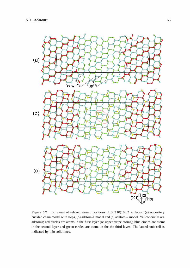
5.3. Adatoms 65
Figure 5.7 Top views of relaxed atomic positions of Si(110)16×2 surfaces: (a) oppositelybuckled chain model with steps, (b) adatom-1 model and (c) adatom-2 model. Yellow circles are
adatoms; red circles are atoms in the first layer (or upper stripe atoms); blue circles are atomsin the second layer and green circles are atoms in the the third layer. The lateral unit cell is
indicated by thin solid lines.

5.3. Adatoms 66
are displaced from the surface towards the vacuum region. The dangling bond of the adatom ismore pz-like. Consequently, more or less one electron is transferred from the adatom to the restatom. The same tendency is observed for Ge. The vertical differences between adatom and restatom positions are rather small with 0.31 and 0.26 A for Si and Ge, respectively.
One attempt to accommodate adatoms in appropriate distances and to saturate all danglingbonds is shown in Fig. 5.4(c). According to a common believe one adatom on a c(2×2) unit cellshould allow an arrangement with a complete saturation of the dangling bonds. According toRef. [86] the adatom is bonded to four different atoms in neighbored chains. Bonds with lengthsof 2.4 and 2.6 A should give rise to an extremely large energy gain of more than 1 eV/1×1cell. The results of the careful relaxation of the structure in Fig. 5.4(c) indicate a completelydifferent behavior. The energy gain in Table 5.2 is much smaller; smaller than those of all bond-length-conserving chain reconstructions [e.g. that shown in Fig. 5.4(a) and the 2×1 adatommodel]. The structural data are in agreement with the energetical findings. We derive a muchlarger distance between the adatom and the fourth (most distant) atom that contributes to theseemingly fourfold coordination of the adatom. The different results (with respect to Ref. [86])can be related to a better convergence concerning the number of atomic layers in the slab, theBZ sampling, and the energy cutoff of the plane-wave expansion. The critical distance between
adatom and fourth atom amounts to 2.87 (3.08) A for Si (Ge), i.e., in between a02 and
√
32
a02 . This
value is much larger than the characteristic bond length 2.34 (2.44) A and can be only related toan extremely weak bond. The physical/chemical reasons for the findings are obvious. Si and Geatoms prefer fourfold coordination with tetrahedral bonding. An arrangement of four nearestneighbors in nearly one plane is rather unfavorable. An adatom with a pz-like dangling orbitalcan only have a weak overlap with the dangling bond at the fourth atom. Another configurationwith a stronger wave-function overlap would however induce a remarkable strain in the atomiclayers below. The situation is similar to the case of adatoms on Si and Ge(111) surfaces (cf.Sect. 3.2) or to the 2×1 adatom reconstruction discussed above. The resulting geometry allowsanother interpretation. The adatom and the fourth atom, the chain atom in [001] direction witha remaining dangling bond, represent an adatom-rest atom pair but not a pair with true bonding.
Using 3×1 and 3×2 unit cells we have optimized structures where all dangling bonds of theoriginal (110) surfaces are saturated by adatoms. Such 3×1 and 3×2 reconstructions are shownin Figs. 5.4(d) and 5.4(e), respectively. Each adatom is threefold coordinated. There remainsonly one dangling bond per adatom. The adatom reconstruction models substantially reduce thedangling bond density, the number of dangling bonds per 1×1 unit cell. Instead of two in the1×2 case with buckled chains or one for the 2×1 and c(2×2) adatom models the dangling bonddensity is further reduced to 2/3. However, in contrast to the other adatom reconstructions norest atoms occur. The 3×1 arrangement of the adatoms following each other in [001] direction[Fig. 5.4(d)] is more favorable from the energetical point of view for Si (cf. Table 5.2). In theGe case it is less favorable than the 2×1 adatom reconstruction. These contradictory findingsare similar to those for the (111) surfaces, where the adatom-rest atom pairs on c(2×8) cells arethe most favorable reconstruction elements for Ge but not for Si (cf. Sect. 3.2). Surprisingly, theout-of-phase arrangement of the adatoms within the 3×2 translational symmetry [Fig. 5.4(e)]is much higher in energy (cf. Table 5.2). This fact confirms that Si and Ge(110) surfaces are

5.3. Adatoms 67
Figure 5.8 Wave-function squares at K for the adatom model of the Si(110)2×1 surface. Leftpanel: highest occupied state, right panel: lowest unoccupied state.
“sensitive” with respect to the adatom distributions. To reduce probably the surface stress wealso have tested a structure with two adatom-rest atom pairs but in 2×2 unit cells (not shown).It gains 20 meV per 1×1 cell for Si and 50 meV in the case of Ge in comparison with the 3×2periodicity. However, in both cases the values lie quite far from those for the most favorableadatom reconstructions.
The general weak tendency for a stabilization of a pure adatom structure, in particular forGe, is understandable in terms of the nearly identical bonding behavior of the adatoms and theresulting bands. It is accompanied with metallic band structures as indicated in Fig. 5.5(c) forboth Si and Ge(110)3×1 adatom structures. The low surface energy of the Si(110)3×1 adatomreconstruction and its metallic band structure do not contradict the reconstruction rules for semi-conductor surfaces [44]. Similar observations have been made for [111] surface orientations.The Si(111)7×7 surface possesses a metallic band structure but is the energetically most favor-able reconstruction. In the Ge(111) case the lowest-energy structure c(2×8) is semiconducting(cf. Sect. 3.2). This is in agreement with the fact that the Ge(110)2×1 adatom reconstruction isalso the lowest one in energy (cf. Table 5.2).
A possible 16×2 reconstruction for Si(110) with a trench where adatoms reduce a maximumnumber of DBs on the terraces is shown in Fig. 5.7(b). The same rebonding mechanism of DBssituated at step atoms is assumed as discussed in the case of Fig. 5.7(a). In the first adatommodel these edge atoms form lines exactly along the [112] direction. Excluding the four stepatoms with nominally two DBs, 28 DBs occur at the surface atoms on the upper terrace beforeadatom coverage. The same number of DBs remain on the lower terrace since four DBs arealready saturated by rebonding with DBs of step atoms on the upper terrace. In Fig. 5.7(b) eightadatoms have been arranged on each terrace to leave only four rest atoms on each terrace whichmay contribute to the formation of stripes in the STM images. Together with the unsaturatedfour DBs at the uppermost edge atoms a total number of 28 DBs remain in a whole 16×2 unitcell instead of the 64 ones in the case of an ideally relaxed (110) surface.
Despite the substantial reduction of the dangling-bond density the model in Fig. 5.7(b) isless stable than a simple bond-rotation relaxation with chains on an unreconstructed Si(110)surface (see Table 3.8). The energy gain due to DB saturation is overcompensated by the stressinduced in the surface. Such a tendency has been discussed above. The actual arrangementof adatoms sensitively influences the system energy. This also holds for the structural elementwith two adatoms marked by a circle in Fig. 5.7(b). It has been proposed previously as a
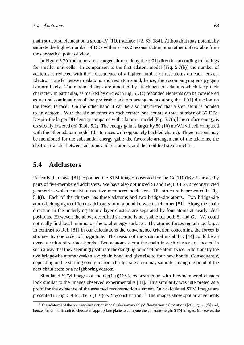
5.4. Adclusters 68
main structural element on a group-IV (110) surface [72, 83, 184]. Although it may potentiallysaturate the highest number of DBs within a 16×2 reconstruction, it is rather unfavorable fromthe energetical point of view.
In Figure 5.7(c) adatoms are arranged almost along the [001] direction according to findingsfor smaller unit cells. In comparison to the first adatom model [Fig. 5.7(b)] the number ofadatoms is reduced with the consequence of a higher number of rest atoms on each terrace.Electron transfer between adatoms and rest atoms and, hence, the accompanying energy gainis more likely. The rebonded steps are modified by attachment of adatoms which keep theircharacter. In particular, as marked by circles in Fig. 5.7(c) rebonded elements can be consideredas natural continuations of the preferable adatom arrangements along the [001] direction onthe lower terrace. On the other hand it can be also interpreted that a step atom is bondedto an adatom. With the six adatoms on each terrace one counts a total number of 36 DBs.Despite the larger DB density compared with adatom-1 model [Fig. 5.7(b)] the surface energy isdrastically lowered (cf. Table 5.2). The energy gain is larger by 80 (10) meV/1×1 cell comparedwith the other adatom model (the terraces with oppositely buckled chains). Three reasons maybe mentioned for the substantial energy gain: the favorable arrangement of the adatoms, theelectron transfer between adatoms and rest atoms, and the modified step structure.
5.4 Adclusters
Recently, Ichikawa [81] explained the STM images observed for the Ge(110)16×2 surface bypairs of five-membered adclusters. We have also optimized Si and Ge(110) 6×2 reconstructedgeometries which consist of two five-membered adclusters. The structure is presented in Fig.5.4(f). Each of the clusters has three adatoms and two bridge-site atoms. Two bridge-siteatoms belonging to different adclusters form a bond between each other [81]. Along the chaindirection in the underlying atomic layer clusters are separated by four atoms at nearly idealpositions. However, the above-described structure is not stable for both Si and Ge. We couldnot really find local minima on the total-energy surfaces. The atomic forces remain too large.In contrast to Ref. [81] in our calculations the convergence criterion concerning the forces isstronger by one order of magnitude. The reason of the structural instability [44] could be anoversaturation of surface bonds. Two adatoms along the chain in each cluster are located insuch a way that they seemingly saturate the dangling bonds of one atom twice. Additionally thetwo bridge-site atoms weaken a σ chain bond and give rise to four new bonds. Consequently,depending on the starting configuration a bridge-site atom may saturate a dangling bond of thenext chain atom or a neighboring adatom.
Simulated STM images of the Ge(110)16×2 reconstruction with five-membered clusterslook similar to the images observed experimentally [81]. This similarity was interpreted as aproof for the existence of the assumed reconstruction element. Our calculated STM images arepresented in Fig. 5.9 for the Si(110)6×2 reconstruction. 1 The images show spot arrangements
1 The adatoms of the 6×2 reconstruction model take remarkably different vertical positions [cf. Fig. 5.4(f)] and,hence, make it difficult to choose an appropriate plane to compute the constant-height STM images. Moreover, the

5.5. Missing rows and adatoms 69
Figure 5.9 Simulated STM images of empty (top panel) and filled (bottom panel) states of the6×2 five-membered clusters Si(110) surface for voltages corresponding to 2 and −2 eV with
respect to the theoretical Fermi level.
similar to the observed pentagon-shaped ones. States originating from all adcluster atoms in-cluding the bridge-site atoms contribute to the empty-state image of the 6×2 reconstruction. Incontrast, in Fig. 5.9 (bottom panel) occupied states give only contributions at bridge-site atomsand not at the other adatoms. We have also not found any contribution of occupied states whichare located at adatoms using a three-dimensional representation of the wave functions. If theplane to plot the constant-height STM images is closer to the surface, it is, however, more prob-able to see states localized at the four rest atoms belonging to the chain. In general, it is notpossible to observe significant pentagon structures in both empty and occupied images for thedescribed Si(110)6×2 reconstruction. This holds also for Ge.
5.5 Missing rows and adatoms
In order to model the 16×2 reconstruction an additional degree of freedom is due to the possi-bility of atom removal or even missing rows of atoms [82, 183]. One possible realization wassuggested by the filled-state STM images of Si(110)16×2 with only six protrusions per unitcell on each terrace. According to Packard and Dow [82] the basic building block consists ofmissing rows of atoms along [110] and adatoms. The corresponding relaxed surface geome-try is shown in Fig. 5.10(a). The atom removal along the [110] direction is clearly visible. Incomparison to the two adatom models in Figs. 5.7(b) and 5.7(c), there is also another type of
comparison of the images obtained in constant-height mode with measured constant-current mode images is ratherproblematic. We use a plane which crosses the bridge-site atoms.

5.6. Tetramers and interstitials 70
adatoms which connect atoms in different atomic layers along [001]. Their situation seems tobe reasonable because these atoms take positions similar to the T4 and H3 adatoms positionson the Si(111) surface (see Sect. 3.2 and Ref. [44]). Six adatoms form a stretched hexagon[marked by dotted lines in Fig. 5.10(a)] with one adatom in the center. Additionally two so-called dimers [82] marked by elongated circles in Fig. 5.10(a) occur between the second andthird atomic layers. These elements have exactly the same bonding nature as the rebonded edgeatoms discussed above.
The 16×2 reconstruction in Fig. 5.10(a) results in the highest surface energy for the geome-tries under consideration. The energy gain amounts to a value being only one half of the gainfor a reconstruction with differently buckled chains shown in Fig. 5.10(a) (cf. Table 5.2). Tworeasons should be mentioned. Locally the adatom distribution is rather similar as in the c(2×2)adatom configuration, which was found to be rather unfavorable. Furthermore, the removal ofatoms to generate the missing rows leave dangling bonds bonds in not preferable configurations.
5.6 Tetramers and interstitials
For Si(110)16×2 the trials to explain the details of the stripes found by STM on different ter-races [72, 75, 82] are focused on structural elements which are able to describe both the empty-state and filled-state images. Another guiding principle should be oriented to the insulatingbehavior observed experimentally for the Si(110)16×2 surface [184]. Pure adatom reconstruc-tions discussed above with partially occupied bands give rise to a metallic character. Danglingbonds situated at pairs of adatoms and rest atoms may give nonmetallic electronic structures butdouble the number of structural elements and, moreover, increase the distance of equally filledDBs. At least, they have to be combined with other reconstruction elements such as dimers onSi(100) [44], tetramers on Si(113) (chapter 4) and (114) [165] or pentamers on Si(113) (chap-ter 4). Indeed, tetramers are able to give rise to different STM images probing empty or filledstates. Using such an element this has been demonstrated for the Si(113)3×2 surface within theADI model and the Si(114)2×1 surface reconstruction with dimers, tetramers, and rebondedatoms [165]. For the Si(113)2×1 surface it has been proven that the pure tetramer structuresyield to a surface-state gap independently of buckling/puckering of the tetramers. Buckled pen-tamers have been predicted to be seen in STM images at negative and positive bias voltages ofthe Si(113)3×2 surface with an adatom-interstitial reconstruction.
One may expect the occurrence of qualitatively similar reconstruction elements on theSi(110)16×2 surface. Based on the idea to explain the STM findings for Si(110)16×2 surfacesby pentagons which are formed by tetramer and interstitial atoms [75], we have studied suchreconstruction elements in 3×2 unit cells. We followed the ideas developed to interpret the 3×2reconstruction of Si and Ge(113) surfaces by ADI and AI models (cf. chapter 4). The pentagon(or pentamer) in one half of a 3×2 cell consists of four adatoms (tetramer) and one atom be-longing to a chain in the first atomic layer. They saturate five of the six surface dangling bonds.The interstitial atom is laterally located at the center of the pentamer but below the pentamerplane. In the second half of the 3×2 cell two additional adatoms saturate the dangling bonds in

5.6. Tetramers and interstitials 71
Figure 5.10 Top views of relaxed atomic positions of Si(110)16×2 surfaces: (a) stretched-
hexagon model, (b) tetramer-interstitial model, and (c) adatom-tetramer-interstitial model. Yel-low circles are adatoms; red circles are atoms in the first layer (or upper stripe atoms); bluecircles are atoms in the second layer and green circles are atoms in the the third layer. The
lateral unit cell is indicated by thin solid lines.
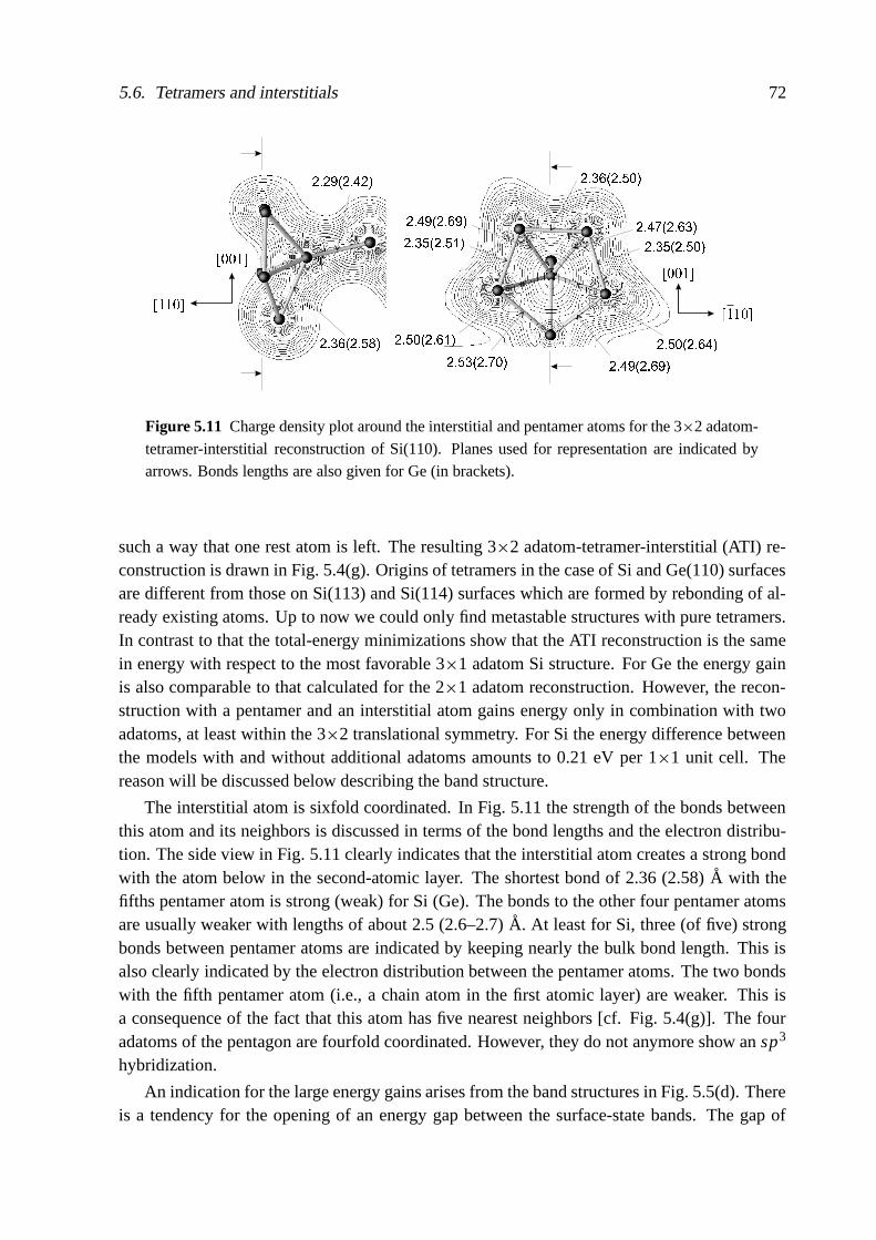
5.6. Tetramers and interstitials 72
Figure 5.11 Charge density plot around the interstitial and pentamer atoms for the 3×2 adatom-
tetramer-interstitial reconstruction of Si(110). Planes used for representation are indicated byarrows. Bonds lengths are also given for Ge (in brackets).
such a way that one rest atom is left. The resulting 3×2 adatom-tetramer-interstitial (ATI) re-construction is drawn in Fig. 5.4(g). Origins of tetramers in the case of Si and Ge(110) surfacesare different from those on Si(113) and Si(114) surfaces which are formed by rebonding of al-ready existing atoms. Up to now we could only find metastable structures with pure tetramers.In contrast to that the total-energy minimizations show that the ATI reconstruction is the samein energy with respect to the most favorable 3×1 adatom Si structure. For Ge the energy gainis also comparable to that calculated for the 2×1 adatom reconstruction. However, the recon-struction with a pentamer and an interstitial atom gains energy only in combination with twoadatoms, at least within the 3×2 translational symmetry. For Si the energy difference betweenthe models with and without additional adatoms amounts to 0.21 eV per 1×1 unit cell. Thereason will be discussed below describing the band structure.
The interstitial atom is sixfold coordinated. In Fig. 5.11 the strength of the bonds betweenthis atom and its neighbors is discussed in terms of the bond lengths and the electron distribu-tion. The side view in Fig. 5.11 clearly indicates that the interstitial atom creates a strong bondwith the atom below in the second-atomic layer. The shortest bond of 2.36 (2.58) A with thefifths pentamer atom is strong (weak) for Si (Ge). The bonds to the other four pentamer atomsare usually weaker with lengths of about 2.5 (2.6–2.7) A. At least for Si, three (of five) strongbonds between pentamer atoms are indicated by keeping nearly the bulk bond length. This isalso clearly indicated by the electron distribution between the pentamer atoms. The two bondswith the fifth pentamer atom (i.e., a chain atom in the first atomic layer) are weaker. This isa consequence of the fact that this atom has five nearest neighbors [cf. Fig. 5.4(g)]. The fouradatoms of the pentagon are fourfold coordinated. However, they do not anymore show an sp3
hybridization.
An indication for the large energy gains arises from the band structures in Fig. 5.5(d). Thereis a tendency for the opening of an energy gap between the surface-state bands. The gap of

5.6. Tetramers and interstitials 73
Figure 5.12 Simulated STM images of filled (left panel) and empty (right panel) states of the
Si(110)3×2 adatom-tetramer-interstitial surface for voltages corresponding to −2 and 2 eV withrespect to the theoretical Fermi level.
the 3×2 ATI reconstruction is the largest one among all studied Si(110) reconstructions. Theopening mechanism is similar to that discussed for the Si(113)3×2 ADI surface. Due to theweak bonding pentamer atoms donate electrons to the two adatoms in the second half of the3×2 unit cell. Their dangling bonds are fully occupied with electrons which form lone pairs. Asa consequence the filled-state (empty-state) STM images are dominated by adatom (pentamer-atom) electronic states. This is demonstrated in Fig. 5.12. For the Si(110)3×2 ATI surface theSTM images simulated for a bias of −2V (2V) mainly show the adatoms (pentamer atoms) inthe lower (upper) half of the 3×2 surface unit cell. The STM image simulated for the emptystates seems to be similar to the characteristic pentagon-shaped element of the empty-state STMimages observed for the Si(110)16×2 surface.
There is a chance that tetramer-interstitial pairs explain the “pairs of pentagons” as sug-gested by An et al. [75]. Such a 16×2 tetramer-interstitial (TI) model is represented in Fig.5.10(b). We adapted the step configuration discussed in Fig. 5.7(a). The connecting line of thechain atom and the interstitial in the resulting centered pentamer is almost parallel to the [001]direction. The uncovered regions of the terraces exhibit the usual bond-rotation relaxation ofthe surface chains.
The TI reconstruction gives rise to a minimum on the total-energy surface but the resultingsurface energy is too high (cf. Table 5.2). The energy gain only amounts to 0.39 eV/1×1 cell.The small gain is in agreement with the findings for a 3×2 translational symmetry. For thatreason the adsorption of two additional atoms for each pentamer is considered. The resulting16×2 ATI geometry is represented in Fig. 5.10(c). Indeed, the surface energy is lowered sub-stantially by 100 meV/1×1 cell with respect to the TI case without additional adatoms. Thisstrong energy gain is mainly due to the strong s character of the DBs situated at the adatomswhich induces an electron transfer from the pentamers resulting in lone pairs of electrons. In-stead of the eight adatoms per 16×2 unit cell we have also studied geometries with 12 or fouradatoms. The accompanying energy gains were only 10−15 meV/1×1 cell lower than for theeight-adatom case. Therefore, we conclude that the number of adatoms per pentamer may varyon real surfaces at room temperature (with kBT = 25 eV) and above.
In any case the ATI reconstruction in Fig. 5.10(c) yields the lowest surface energy for mod-els of the Si(110)16×2 surface with trenches and terraces. However, the corresponding energy

5.6. Tetramers and interstitials 74
gain of 0.49 eV/1×1 cell is still smaller than the gain of 0.54 eV/1×1 cell obtained for the ATIreconstruction of the Si(110)3×2 surface. Since this energy difference is not a consequence ofthe numerical inaccuracy of the total energy calculations, it has to be discussed physically. Ei-ther the 16×2 reconstruction does not represent the equilibrium surface phase or a completelydifferent reconstruction model is needed. Kinetic barriers and hence the surface preparation usu-ally allow the observation of the 16×2 phase only for less doped substrates. Such a preparationdependence is known for the Si(111) surface with the 2×1 reconstruction after low-temperaturecleavage and the 7×7 translational symmetry after annealing [44]. Perhaps, a completely new,more complex reconstruction model is needed such as the DAS model with corner holes foundfor the Si(111)7×7 surface [62]. At least the total energy investigations of the 16×2 recon-struction models suggested by several authors [75, 82] and the 16×2 geometries lead to surfaceenergies higher than that calculated for the 3×2 translational symmetry.
Besides the surface energy other important arguments for the validity of a certain recon-struction model can be derived from STM images simulated for different bias voltages. Suchimages are presented in Fig. 5.13 for the 16×2 ATI reconstruction. Because of the constant-height mode used in the simulation only spots from upper terraces are visible. The figure showsthat the observed image stripes can really be simulated by an ATI reconstruction. The stripesparallel to [112] consist of pairs of extended reconstruction elements arranged in zigzag form.They are based on pentamers and accompanied by an additional pair of adatoms. The interstitialatoms captured by the pentamers are not seen. Indeed, Fig. 5.13 shows that one and the samereconstruction element gives rise to different spot distributions in the empty-state or filled-stateimages in agreement with the experimental observation [75].
Each element in the empty-state images consists of nearly five spots and represents directlythe pentagon. The filled-state images in Fig. 5.13 show two strong spots due to the filled DBsat the adatoms and four weak spots from the tetramer which may be unified in the simulationvarying the distance to the surface. Important features found experimentally can be reproducedbut not all. Comparing with the analysis of An et al. [75] (see Fig. 5.14) the fine structure of thepairs seems to be interchanged in the measured and calculated spot distributions. On the otherhand, the filled-state images measured by Packard and Dow [82] have been interpreted by anarrangement of spots in a deformed hexagon with a center. In contrast to the images discussedabove only six spots belong to one terrace in a 16×2 unit cell. There is also disagreementbetween experimental results. One explanation for the different findings may be related to theenergetics of the adatom-tetramer-interstitial reconstruction mentioned above. The variation ofthe number of adatoms (which should give rise at least to spots in the filled-state images) doeshardly influence the surface energy.
Other points to be discussed concern the visibility of the interstitial atoms and the asymme-try (buckling, puckering) in the pentamer or tetramer structures. Hints follow from the behaviorof the Si(113)3×2 surface. For this surface the ADI model represents a low-energy structure.After addition of one interstitial to each tetramer the AI 3×2 model appears having two pen-tamers and two adatoms similar to the ATI reconstruction considered in Fig. 5.13(c). Asymme-tries between the two pentamers in the Si(113)-AI model allow an additional electron transferthat lowers the energy. It has been shown that the presence of interstitials and asymmetries
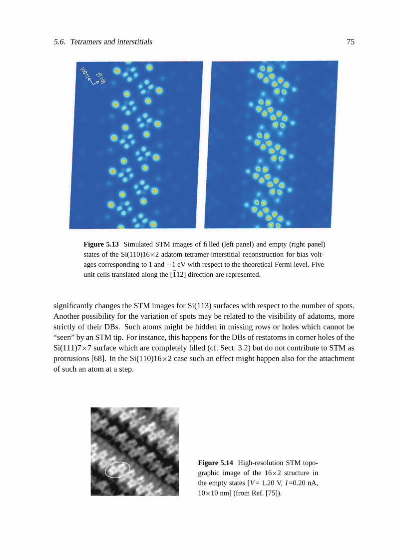
5.6. Tetramers and interstitials 75
Figure 5.13 Simulated STM images of filled (left panel) and empty (right panel)
states of the Si(110)16×2 adatom-tetramer-interstitial reconstruction for bias volt-ages corresponding to 1 and −1 eV with respect to the theoretical Fermi level. Fiveunit cells translated along the [112] direction are represented.
significantly changes the STM images for Si(113) surfaces with respect to the number of spots.Another possibility for the variation of spots may be related to the visibility of adatoms, morestrictly of their DBs. Such atoms might be hidden in missing rows or holes which cannot be“seen” by an STM tip. For instance, this happens for the DBs of restatoms in corner holes of theSi(111)7×7 surface which are completely filled (cf. Sect. 3.2) but do not contribute to STM asprotrusions [68]. In the Si(110)16×2 case such an effect might happen also for the attachmentof such an atom at a step.
Figure 5.14 High-resolution STM topo-graphic image of the 16×2 structure inthe empty states [V = 1.20 V, I =0.20 nA,
10×10 nm] (from Ref. [75]).

Chapter 6
Shape of free and constrained crystallites:Influence of surface energies
6.1 Absolute Surface Energies
6.1.1 Dependence on orientation and reconstruction
Here we summarize values of absolute surface energies given in previous chapters for the mostfavorable reconstruction and make comparative studies for different orientations and materials.Resulting values are listed in Table 6.1. If one again imagines cutting a group-IV crystal atsome plane, one may expect the energy required to be proportional to the number of bonds cut.In units of a−2
0 (a0 - bulk lattice constant) the dangling-bond density across a {111} surfaceplane is 4/
√3. This is smaller than the density of 2
√2 on a {110} surface, 12/
√11 on a {311}
surface and 4 on a {100} surface. With exception of diamond the trends in the energies of theunrelaxed/unreconstructed Si and Ge surfaces follow the dangling-bond densities. However, af-ter inclusion of surface reconstruction the {111} surfaces of diamond possess the lowest energy,and therefore one may expect the natural cleavage plane or growth surface to be a {111} plane.There are eight such orientations, forming the eight faces of the natural octahedral crystal forthe homopolar tetrahedral solids. The ordering of the other surface energies is more compli-cated to understand. With surface reconstruction the {311} faces seem to be favored againstthe {110} planes (cf. e.g. in the case of diamond). This is in agreement with the dangling-bond densities if only the dangling bonds in the uppermost atomic layer of the {311} surfaceare counted. The high surface energies γ (110) for silicon and germanium in Table 6.1 reflectthe small energy gain of only about 0.5 eV/1 × 1 unit cell even studying the long-range 16 × 2reconstructions. The absolute surface energies of the reconstructed {111}, {311}, and {100} sur-faces of germanium are practically equal. The smaller values for {311} and {100} of about 0.01J/m2 (i.e., about 1%) with respect to the {111} cases may be considered as the inaccuracy (moreprecisely, numerical uncertainties treating slabs with different orientations) of the used ab initiocalculations (see chapter 2).
The order of magnitude of the values measured for Si [27] (see Table 6.1) agrees very wellwith the energies calculated for the reconstructed surfaces. This also holds more or less for
76

6.1. Absolute Surface Energies 77
Table 6.1 Surface energies γ (in J/m2) for diamond, Si and Ge (see also Tables3.1, 3.4, 4.1 and 5.2). The first value represents the unrelaxed {hkl} surface, while
the second (lower) value corresponds to the reconstructed/relaxed geometry withthe lowest energy. In the case of Si the results are compared with those of measure-
ments [27] (the absolute scale is set using the value γ (111) from fracture experi-ments [185]) tight-binding calculations [38], and molecular dynamics with empiri-cal potentials. [39] A reconstruction is not taken into account. Only the measured
γ (111) value should be related to the 2 × 1 reconstruction [185].
Crystal {111} {110} {100} {311} Reference
Diamond 8.12 7.48 9.72 8.34
4.06 5.93 5.71 5.11 present work
Silicon 1.82 2.04 2.39 2.21
1.36 1.63 1.41 1.40 present work
1.23 1.43 1.36 1.38 [27]
1.41 1.57 1.34 1.98 [38]
1.41 1.72 1.49 – [39]
Germanium 1.32 1.51 1.71 1.61
1.01 1.14 1.00 0.99 present work
the energetical ordering γ (111) < γ (311) < γ (100) < γ (110). Within the experimentalresults only the sequence of the {311} and {100} planes is interchanged. However, their energydifference is small in theory and experiment. The ordering obtained in other calculations [38,39] is the same. The other available experiment [26] found a surprisingly small anisotropy of thesurface excess free energy per unit area with a strange hierarchy γ (100) < γ (311) < γ (110) ≤γ (111) which is not in agreement with the fact that cleavage happens for {111} surfaces. Theanisotropy of the surface energies in Table 6.1 is remarkably increased for diamond, while italmost vanishes for germanium.
Table 6.1 also shows that the surface reconstruction and hence the actual surface geometryand preparation should play an important role for the shapes of crystallites or nanopyramids.The maximum change with respect to the energy of the surface with a bulk atomic arrangementamounts to 100% for the C(111) surface after a 2 × 1 reconstruction within the π -bonded chainmodel. For Si(111) with the most favorable 7 × 7 reconstruction and Ge(111) with the c(2 × 8)reconstruction the effect is much weaker. Similar observations are made for the 2 × 1 (C) orc(2 × 4) (Si, Ge) reconstructions of a {100} surface. The energy of Si and Ge(311) surfaces issubstantially lowered by 3 × 2 ADI reconstructions. Indeed, there are experimental indicationsfor reconstructed {311} surfaces on nanostructures. Pyramidal Si islands appearing at finitegrowth temperature on Si(001) substrates have {311} facets with a seemingly 3×1 reconstruc-tion [31]. In the case of C(311) again a deviating behavior is found with a symmetric 2 × 1tetramer reconstruction. In the {110} cases the surface relaxation within a bond-contraction or a

6.2. Equilibrium Crystal Shape 78
bond-rotation model lowers the surface energy. Complicated long-range 16×2 reconstructionsgive only rise to a small additional energy gain (listed for Si) even considering ATI structuralelements. In Table 6.1 we present the lowest surface energy values found for 3×2 ATI and 2×1adatom models for Si and Ge, respectively.
6.1.2 Extrapolation
In order to investigate 〈100〉-oriented nanocrystals with pyramidal shape, one also needs thesurface energies of {501} or {301} planes. Unfortunately, parameter-free calculations are notavailable for the absolute surface energies for the surfaces with those orientations. Such cal-culations [16, 186] are restricted to the reconstruction geometries and the electronic structures.To estimate the γ (501) and γ (301) values we use the assumption that the surface free energy γvaries only weakly with the surface crystallographic orientation.
We formally consider a two-dimensional crystal in a plane perpendicular to the [010] direc-tion with a vicinal surface plane, i.e., a surface plane which consists of a relatively high numberof areas with [100] orientation being separated by steps of a certain height sn [10]. Such asurface has an orientation angle θ against the [100] direction. Each step is assumed to make acontribution δ to the total surface energy on the vicinal plane. With a step density tan θ/sn onecan express the surface energy as
γ (θ) = γ (100) cos θ + δ
snsin θ. (6.1)
The orientation vector [101] of the closest high-index surface (101) is found for θ =45◦. Assuming a continuous variation of the surface energy between the minima at [100]to [101] [26, 27], one finds δ/sn =
√2γ (110) − γ (100). In the case of the [n01] orienta-
tion (n = 5, 3, 1) it holds θ = 11.31◦, 18.43◦, 45◦. Then expression (6.1) gives γ (n01) =(1/
√n2 + 1)[(n − 1)γ (100) +
√2γ (110)]. One finds the energy values γ (501) = 6.12 (C),
1.56 (Si), and 1.10 (Ge) J/m2 and γ (301) = 6.26 (C), 1.62 (Si), and 1.14 (Ge) J/m2 using thevalues for reconstructed low-index surfaces from Table 6.1.
6.2 Equilibrium Crystal Shape
6.2.1 Shape of diamond crystallites
Results of the Wulff construction of the ECS for diamond are plotted in Fig. 6.1. Essentiallythe surface energies calculated for the reconstructed low-index surfaces from Table 6.1 havebeen used. Taking into account only the surface with the lowest energy γ (111) = 4.06 J/m2,the cleavage face, one expects that the equilibrium geometry is a regular octahedron with eight{111} facets. However, already the inclusion of one further surface orientation such as {100}[as shown in Fig. 6.1(a)] makes the octahedron irregular. The corners of the octahedron aretruncated by {100} planes. A cubo-octahedron morphology appears with eight nonideal {111}hexagons and six {100}-oriented squares. Their areas depend on the surface energies, as long

6.2. Equilibrium Crystal Shape 79
Figure 6.1 Equilibrium shapes of diamond crystals based on the Wulff construction using basi-
cally γ values from Table 6.1. In general, four surface orientations are considered, but in (a) only{111} and {100} facets. (b): Instead of the energy for the 2 × 1 reconstruction γ (311) = 5.11J/m2 that for the 3×1 reconstruction γ (311) = 5.50 J/m2 is taken into account. (c): Values from
Table 6.1. (d): Values as for (b) but the energy of {110} facets is reduced to γ (110) = 4.91 J/m2.The areas with the orientation sequence 〈100〉, 〈311〉, 〈110〉, and {111} are red, green, grey, and
blue.
as√
3γ (111) < γ (100) [124]. If γ (111) is considerably less than γ (100) no truncation isexpected. In the opposite limit a constant ratio of the plane areas occurs.
Taking into account more surface planes with other orientations, the resulting shape dependsvery much on the absolute values of the surface energies. This is also clearly demonstrated inFig. 6.1. Using the energy γ (311) = 5.50 J/m2 for the symmetric 3×1 AD reconstructioninstead of the lower value given in Table 6.1 [Fig. 6.1(b)], the cubo-octahedral shape of thenanocrystallites is basically conserved; but the {100} squares are surrounded by stripes corre-sponding to {311} facets. Diamond particles with exactly such a morphology have been ob-served after deposition by microwave-plasma CVD [35]. Decreasing the surface energy of the{311} facets to the value γ (311) = 5.11 J/m2 (Table 6.1) for the 2×1 reconstruction, the cornertruncation does not anymore happen, and no {100} facets occur [see Fig. 6.1(c)]. Instead, theoctahedron corners are rounded by small square-based pyramids with four {311} facets. An-other example for the strong influence of the absolute γ values is shown in Fig. 6.1(d). Thevalues constructing Fig. 6.1(b) have been used but the surface energy of the {110} planes isreduced to γ (110) = 4.91 J/m2. In contrast to Fig. 6.1(b) the sharp edges between {111} facetsdisappear, and {110} planes form stripes along the former edges. Such a shape with {111},{100}, {311}, and {110} facets has been observed for high pressure–high temperature syntheticdiamonds [34]. Their surfaces have major growth sectors of the {111} and {100} types and someminor sectors of {311} and {110} types.
Despite the agreement stated for the ECSs in Fig. 6.1with morphologies observed for growndiamond crystallites, general conclusions are very difficult. There is perhaps not a direct rela-tionship between absolute surface energies of reconstructed clean surfaces and crystallographythat the above description suggests. The real surfaces may be contaminated by adsorbed speciesor influenced by defects. Adsorbates and defects may change the surface reconstruction and,hence, the corresponding surface energy. In addition, the observed crystallite shapes may tendto be dominated by the growth process of the crystal rather than the energetics itself. One fact is

6.2. Equilibrium Crystal Shape 80
Figure 6.2 Equilibrium shapes of Si (a, b) and Ge (c, d) crystals based on the Wulff constructionusing (a) experimental values, (b, c) calculated values or (d) equal values γ for many surface ori-entations in the stereographic triangle [188]. In (a, b, c) four surface orientations are considered.
The areas with the orientation sequence 〈100〉, 〈311〉, 〈110〉, and 〈111〉 are red, green, grey, andblue. In (d) more high-index surfaces are taken into consideration. The facets in yellow, violet,
and light blue represent {331}, {21 9 29}, and {15 3 23} facets, respectively.
related to the orientation dependence of the growth rate. For instance, there are indications thatthe CVD growth rate on {100} surfaces is faster than that of the {111} side-growth rate [187].The preferential growth along a 〈100〉 direction clearly influences the resulting morphology ofa crystallite.
6.2.2 Shape of Si and Ge crystallites
Figure 6.2 shows results of the Wulff construction of the ECS for silicon and germanium. InFigs. 6.2(b) and 2(c) we used calculated parameters of the surface energies γ (hkl) for the re-constructed {111}, {110}, {100}, and {311} surfaces of silicon and germanium given in Table6.1. For the purpose of comparison the ECS for Si is presented in Fig. 6.2(a) for measuredsurface energies [27]. According to energies given in Table 6.1, Fig. 6.2(a) shows that the moststable surfaces have an 〈111〉 orientation with the next lowest ones being {100}, {311}, and{110} surfaces with similar energies. Large {111} facets and smaller {100} facets occur on thesurface of a crystallite. Between these facets smaller {311} and {110} facets are observable.No sharp edges between a {111} and a {100} facet or between two {111} facets appear. Ac-cording to the experimental γ values the equilibrium shape is thus to a good approximation atetra-kaidecahedron [27]. Taking the calculated γ values into account the {110} facets almostvanish as a consequence of the large γ (110) value as shown by their small contributions in thecorners between four {311} facets in Fig. 6.2(b). In addition the areas of the {311} facets areincreased because of the low value of γ (311).
One of the results of the ECS construction is the possible stability evaluation of a surfacewith a certain orientation. We have checked a possible occurrence of the Si(411) surface on theECS. A Si(411)2×1 reconstruction has been observed experimentally. The value of its surfaceenergy calculated within an ab initio method lies between those for (111)2×1 and (100)2×1surfaces [165]. Consequently, it has been concluded that Si(114) is a stable planar surface [165].

6.3. Shape of Pyramidal Nanocrystals 81
To be consistent within the computational method used here we assume γ of Si(411)2×1 to beequal to 1.44 J/m2 as found for the lowest left buckled π -bonded chain Si(111)2×1 reconstruc-tion from our calculations. Surprisingly, despite such a low γ the {411} facets do not occur onthe ECS indicating that a (114) surface is not stable in the equilibrium in contrast to the (100)or (311) ones. However, narrow stripes would appear between the {100} and {311} facets ifan additional reduction of about 0.015 J/m2 is assumed, what also indicates that the absence of{411} facets might be related to inaccuracy of our approximations. The sensitivity of the ECSwith respect to the absolute values of the surface energies again shows that modifications of thefacet geometry, e.g. due to reconstruction, may drastically change the surface morphology of acrystal.
The last tendency is enforced for germanium as demonstrated in Fig. 6.2(c). Since theenergies for the surface orientations 〈111〉, 〈311〉, and 〈100〉 are nearly the same, large {111},{311} and {100} facets are visible. However, {311} facets give the largest area. Only smalldiamond-shaped {110} planes occur between {311} facets (note, larger than in the the case ofSi). Nearly equal energies of the most stable surface orientations give a probability that severalother high-index orientations have a similar γ and are therefore stable in the Ge case. To checkthis we include possible candidates with equal γ . In addition to the above-mentioned foursurface orientations we also study the high-index surfaces {313}, {15 3 23} and {21 9 29} whichhave been reported to be stable and, hence, do not facet into other stable surfaces [188]. Theresulting ECS is represented in Fig. 6.2(d). All considered surface orientations appear on it. Ingeneral, a Ge crystal tries to reach a “sphere” shape. The largest facets are {111}, {311} and{100} ones, while the {110} facets occur with a smaller area. Each of the sets of real high-index{15 3 23} or {21 9 29} surfaces contributes to the 48 facets. The corresponding values of the totalarea per each family are close to that for {311} facets which take the largest area.
6.3 Shape of Pyramidal Nanocrystals
6.3.1 Total energy and surface energy
The shape of a large, isolated, three-dimensional island grown on a certain substrate is deter-mined by its total energy [9, 189]
Etotal = Eelastic + Esurface + Eedge. (6.2)
For coherently strained or partially relaxed islands the leading terms are the elastic relaxationenergy Eelastic and the surface energy Esurface of the strained object connected with a substrate.Eelastic is the gain in deformation energy when the material forms a strained island instead ofa biaxially strained film. Esurface is the cost in surface energy due to the creation of facetson the sides of the island corrected by the fact that the island base forms an interface to thesubstrate or the corresponding wetting layer. Eedge is the energy cost for the creation of sharpedges. Because of the interplay of local strain distribution and shape the scaling behavior ofEelastic with the volume V may also include nonlinear terms in addition to the main linear term.
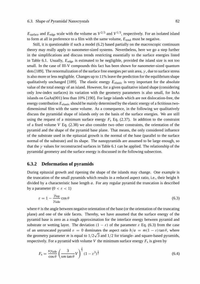
6.3. Shape of Pyramidal Nanocrystals 82
Esurface and Eedge scale with the volume as V 2/3 and V 1/3, respectively. For an isolated islandto form at all in preference to a film with the same volume, E total must be negative.
Still, it is questionable if such a model (6.2) based partially on the macroscopic continuumtheory may really apply to nanometer-sized systems. Nevertheless, here we go a step furtherin the simplifications and discuss trends restricting essentially to the surface energies listedin Table 6.1. Usually, Eedge is estimated to be negligible, provided the island size is not toosmall. In the case of III-V compounds this fact has been shown for nanometer-sized quantumdots [189]. The renormalization of the surface free energies per unit area, γ , due to surface stressis also more or less negligible. Changes up to 11% leave the prediction for the equilibrium shapequalitatively unchanged [189]. The elastic energy Eelastic is very important for the absolutevalue of the total energy of an island. However, for a given qualitative island shape (consideringonly low-index surfaces) its variation with the geometry parameters is also small, for InAsislands on GaAs(001) less than 10% [190]. For large islands which are not dislocation-free, theenergy contribution Eelastic should be mainly determined by the elastic energy of a fictitious two-dimensional film with the same volume. As a consequence, in the following we qualitativelydiscuss the pyramidal shape of islands only on the basis of the surface energies. We are stillusing the request of a minimum surface energy Fs Eq. (2.37). In addition to the constraintof a fixed volume V Eq. (2.38) we also consider two other constraints, the orientation of thepyramid and the shape of the pyramid base plane. That means, the only considered influenceof the substrate used in the epitaxial growth is the normal of the base (parallel to the surfacenormal of the substrate) and its shape. The nanopyramids are assumed to be large enough, sothat the γ values for reconstructed surfaces in Table 6.1 can be applied. The relationship of thepyramidal geometry and the surface energy is discussed in the following subsection.
6.3.2 Deformation of pyramids
During epitaxial growth and ripening the shape of the islands may change. One example isthe truncation of the small pyramids which results in a reduced aspect ratio, i.e., their height hdivided by a characteristic base length a. For any regular pyramid the truncation is describedby a parameter (0 < ε < 1)
ε = 1 − γtop
γsidecos θ (6.3)
where θ is the angle between negative orientation of the base (or the orientation of the truncatingplane) and one of the side facets. Thereby, we have assumed that the surface energy of thepyramid base is zero as a rough approximation for the interface energy between pyramid andsubstrate or wetting layer. The deviation (1 − ε) of the parameter ε Eq. (6.3) from the caseof an untruncated pyramid ε = 0 dominates the aspect ratio h/a = m(1 − ε) tan θ , wherethe geometry parameter m is equal to 1/2
√3 and 1/2 for triangle- and square-based pyramids,
respectively. For a pyramid with volume V the minimum surface energy Fs is given by
Fs = sγside
cos θ
(
3
sm tan θV
)23
(1 − ε3)13 (6.4)
6.3. Shape of Pyramidal Nanocrystals 83
Figure 6.3 Top view of frustum of a [111]-oriented pyramid with {311} facets.
where the geometry parameter s is√
3/4 for the triangle base and 1 for the square base. Thecomparison of the total surface energies for a given volume V gives an indication for the favoredorientations of the facets and the trend for truncation of the pyramid.
Growth of Ge on Si(111) surfaces leads to nucleation of three-dimensional islands whichconsist of {113} facets as side walls and a flat top (111) facet [24]. The model of such a pyra-midal island is presented in Fig. 6.3 with a (111) triangle base, a (111) top, and three equivalent(113), (131) and (311) facets. In this case the angle θ is given by arccos(5/
√33) [i.e., 29.5◦].
During the epitaxial growth the aspect ratio of an island may change as a function of the cov-erage. However, the form of the island is always a frustum of a tetrahedron and the completepyramid with {113} facets is never reached [24]. Using values from Table 6.1 one finds for theparameter ε = 0.31 (C), 0.15 (Si), and 0.11 (Ge). The truncation can be interpreted as a conse-quence of the ECSs presented in Figs. 6.1 and 6.2. They show appearance of large {111} facetsfor diamond and relatively small {111} facets for Ge. A reduction of the surface energies of(111) faces till values corresponding to a 2×1 reconstruction [i.e., 1.45 (Ge) and 1.05 (Si) J/m2]also fulfills the condition for the truncation. For Ge the aspect ratio h/a results to 0.145 [withγ (111) corresponding to c(2 × 8)] or 0.15 [with γ (111) corresponding to 2 × 1]. Indeed, thisvalue varies from 0.1 to 0.135 during the growth [24]. Consequently, taking into account onlysurface energies, there is a tendency for truncation of a [111]-oriented triangle-based pyramidshown in Fig. 6.3.
At low growth temperatures or low Ge coverages the small Ge islands grown on Si(100)substrates are rectangular-based huts or square-based pyramids with {501} [19–22] or some-times {301} [16] facets. In the case of InAs quantum dots on GaAs(100) substrates also {101}facets have been studied [9, 190, 191]. In order to model the pure surface energetics of smallislands of this type, we consider a (001) square base with a [001] normal and four equivalentfacets with [01n], [01n], [10n], and [10n] orientations (n = 1, 3, 5) [see Fig. 6.4(a)]. The tiltangle θ of the facets is given by arccos(n/
√1 + n2) [i.e., 45◦, 18.43◦ or 11.31◦]. The trunca-
tion of the considered pyramids takes place for all group-IV elements. However, the tendencyto cut a pyramid is stronger for the smaller n. For germanium the parameter Eq. (6.3) amountsto ε = 0.37 (n = 1), 0.21 (n = 3) and 0.11 (n = 5). Similar dependencies are found for Si andC. Assuming the value γ (001) = 1.05 J/m2 for Ge, which corresponds to a 2×1 reconstruction,the value of truncation amounts only to ε = 0.06 and the aspect ratio is h/a = 0.006. Experi-

6.3. Shape of Pyramidal Nanocrystals 84
Figure 6.4 Top view of [100]-oriented pyramids or domes with {n01} (n = 5, 3, 1), {n11}(n = 3, 1) and {100} facets. In (d) the facets without denotation represent {15 3 23} facets.
mentally, the latter quantity was observed equal to 0.1 what nearly corresponds to the completepyramid.
At higher Ge coverages of Si(100) substrates large Ge islands, so-called domes, appear.The domes are more rounded and display a multifaceted surface [22]. They are bounded by{113} and {15 3 23} facets. In the intermediate coverage regime also the occurrence of {105} isdiscussed. Here, we neglect the rounding and only study another type of square-based pyramidswith [001] orientation and four equivalent facets with [11n], [11n], [11n], and [11n] surfacenormals where usually n = 3 but also other values such as n = 1 may be considered [see Fig.6.4(b)]. Such shapes have been suggested for Si nanocrystallites [30]. In their case the tilt angleθ of the facets arccos(n/
√n2 + 2), i.e., 54.74◦ (n = 1), 25.24◦ (n = 3), and 6.21◦ (n = 13),
depends dramatically on the growth time. For short growth times even {1 1 13} facets withn = 13 have been observed. They change over into {111} facets with n = 1 for longer growthtime.
Within the simplified picture Eq. (6.4) of the restriction to surface energies, one finds that{n11} facets are more favorable than {n01} facets. For large Ge nanocrystals, this finding is inagreement with the observation of {311} facets instead of surfaces with 〈501〉 orientations [22].According to Eq. (6.4) the total surface energy is three times smaller in the case of {311} facets.
Again, we have to state that the total energy reduction may be also a driving force for thetruncation of the pyramids with 〈n11〉 facet orientations. The largest parameters ε occur for n =1. Using the values from Table 6.1 one has ε = 0.19 (C) and 0.42 (Si and Ge). Consequently,the tendency for truncation is most pronounced for silicon and germanium. For n = 3 for thesematerials the values of ε with 0.09 (Si) and 0.08 (Ge) are much smaller. Truncation will nothappen for n > 1 in the diamond case. For Si islands it has been observed that pyramids with{111} facets transform into ones with 〈311〉 orientation at elevated temperature. Allowing thatboth {113} and {111} facets appear on the side walls the ratio of their heights h(311)/h(111) isgiven by 2γ (001)/[
√11γ (311) −
√3γ (111)] − 1. According to Table 6.1 this results to 0.23
(0.30) for Si (Ge) or 0.32 (0.37) if the energy of (111) surface is reduced to the value for the2×1 reconstruction.

6.3. Shape of Pyramidal Nanocrystals 85
For Si and Ge the main difference between the ECSs derived by Wulff constructions shownin Fig. 6.2 and pyramid shapes discussed in this section (i.e. models of experimentally observedcrystallites) is the number of occurring steep facets. In particular, for [100]-oriented pyramidsone may consider another shell of {311} facets. This would give eight additional {311} ones.But they do not appear on islands during epitaxial growth. The reason seems to be related tothe very large angle θ of these facets with the 〈100〉 orientation, namely 72.45◦. Other facetscorresponding to orientations with smaller θ are more likely. Surfaces with 〈111〉 and 〈110〉orientations with θ equal to 54.74◦ and 45◦, respectively, are good candidates. It is interestingthat {110} facets which almost disappear on the ECS [see Figs. 6.2(b) and 6.2(c)] could leadto large facets on the [100]-oriented pyramid in addition to the discussed four {113} facets.For Si and Ge, in this case four facets with 〈110〉 orientation will occur near the bottom of thepyramid and a rounding of the base will take place [cf. Figs. 6.2(a) and 6.2(b)]. Moreover, forSi pyramids {111} facets have indeed been observed. That is not the case for heteroepitaxiallygrown Ge islands, for which also {110} facets have not been detected. Experimentally observed{15 3 23} facets have only a tilt angle of θ = 33.63◦. A model of such a pyramid is shownin Fig. 6.2(d). Taking into account only surface energies the probability for facets with thissurface orientation to appear in the corner between two neighboring {311} facets is rather high.It happens if the relation γ (15 3 23) . 1.7γ (311) is fulfilled as the condition for the minimumof the total surface energy. As mentioned above for Ge (the softest material under consideration)surface energies of different orientations do not vary so much. Therefore, other effects than theenergetics, e.g. strain, should stabilize such less sloping high-index facets.
For the surface energies given in Table 6.1 with a not too strong variation with the surfaceorientation we conclude that deviations from the ideal shape of the pyramids, such as truncationor rounding, are favorable within considerations restricted to the pure energetics of the facets.However, these results can only indicate a trend. Taking into account the strain of the pyramidsthe volume dependence of the total energy (6.2) is changed from E total = αV
23 to Etotal =
αV23 −βV [192]. Optimizations of energy functionals of such a type may give modified results.
In particular, it is expected that the effects of truncation and rounding depend on the pyramidvolume. Consequently, shape transitions as the transition from pyramids to domes observed forGe on Si(100) can be only described taking into account the strain energy and/or kinetics effectsand not only using an equilibrium theory with a restriction to the total surface energy.
Chapter 7
Summary and conclusions
We have presented extensive first-principles studies of the energetics and the reconstructionsof the clean low-index (111), (110), (100) and high-index (113) surfaces of the three group-IV semiconductors diamond, silicon, and germanium. The calculations have been performedwithin DFT using the LDA and the repeated-slab approximation. Different reconstructions in-cluding the largest ones observed experimentally such as Si(111)7×7 and Si(110)16×2 havebeen investigated. The atomic geometries have been optimized in order to find the minimum ofthe total energy. For these atomic structures the electronic band structures have also been calcu-lated. For the most interesting surface reconstructions STM images have been simulated in orderto make a “direct” comparison with experimentally observed surface images. A combinationof symmetric slabs and slabs with a hydrogen passivation at one side allowed the determina-tion of absolute surface energies not only for unreconstructed surfaces. Such a combination oftwo different slab approximations makes the computations tractable and not too costly also forreconstructed surfaces with large unit cells.
In the case of (111) surfaces we have presented studies for the basic reconstructions 2×1,c(2 × 8), and 7×7. The resulting energetics has been discussed in terms of the most importantstructural parameters and surface band structures of the π -bonded chain, adatom, and dimer-adatom-stacking-fault models. We found that the 2×1 reconstruction gives the lowest energyonly for diamond. Within the theoretical methods used here the strange result of a metallicband structure of the C(111)2×1 surface (measurements reveal an insulating behavior) cannotbe avoided. For Si and Ge, the large 7×7 or c(2×8) reconstructions are energetically more fa-vorable. Chemical trends have been derived that indicate clear differences between the carbonatoms with a lack of p- and d-electrons in the core and the bigger Si or Ge atoms. In particularthe strong C-C bonding is responsible for the absence of long-range adatom-induced recon-structions on C(111). Si and Ge surface structures gain more energy by the electron transferbetween adatoms and rest atoms because of the accompanying smaller subsurface stresses. Inthe intermediate case of silicon, additional reconstruction elements occur to balance the differ-ent tendencies observed for diamond and germanium.
In general, a similar behavior occurs for the (100) surfaces. For Si and Ge, dimers are alwaysasymmetric, the c(4×2) reconstructions are lower in energy than the 2×1 ones. We have alsofound a very small energy difference between the lowest c(4×2) phase and the p(2×2) one.
86

7. Summary and conclusions 87
In contrast, in the diamond case no asymmetric dimers occur at the (100) face. The tendencyfor stabilization of symmetric structures on diamond surfaces and the tendency for symmetryreductions at the Si and Ge surfaces are observed not only for the (111)2×1 and (100)2×1translational symmetries but also for the relaxed (110)1×1 faces, the latter being the groundstate in the diamond case. Any buckling of chains or dimers induces a substantial subsurfacestrain and, hence, makes a symmetry break unlikely in the diamond case. Tilting of chains anddimers on Si and Ge surfaces opens energy gaps between surface states. The accompanyingenergetical lowering of the occupied bands gives rise to an energy gain. Moreover, such atilting allows different chain isomers on the Si and Ge(111) surfaces and the c(4×2) and p(2×2)translational symmetries of the (100) surfaces of Si and Ge.
The 2×1 unit cell with symmetric tetramers has been shown to be the most stable C(113)surface. For the first time, total-energy calculations have been presented for this orientation ofdiamond crystals. Interestingly, the tetramer band structure exhibits a clear insulating character.The surface energy is even lower than that of the C(001)2×1 surface. It could make the C(113)surfaces useful for future applications. Also in the Si(113) and Ge(113) cases, the formationof tetramers tends to give rise to a semiconducting surface. In particular, asymmetries due tothe puckering of the tetramers support the opening of an energy gap between surface states.However, for Si and Ge the situation is more complicated since 3×1 and 3×2 translationalsymmetries have been observed experimentally. The presence of adatoms leads to metallicstructures for all the materials as a consequence of the half-occupied adatom dangling bonds.No structure with tetramers and adatoms can overcome this problem, even assuming a certainasymmetry of the tetramer as it was proposed by several research groups. The Si and Ge(113)surfaces with 3×1 or 3×2 reconstructions have been confirmed to be stabilized only by subsur-face self-interstitials. For germanium two considered interstitial-induced reconstructions, 3×1AI and 3×2 ADI, can hardly be distinguished from an energetical point of view. The 3×2 AIreconstruction gives rise to a global minimum on the total-energy surface. Nevertheless, thesmall energy differences indicate that interstitial migration and coexistence of different surfacephases should be likely. In the Si(113) case, due to a repulsive interaction of the interstitialatoms on short distances, the 3×2 ADI structure has been found to be most favorable. How-ever, the energy differences to the other interstitial reconstructions remain also small. Within thestable reconstructions of the Si and Ge(113) surfaces only the 3×2 AI and 3×2 ADI structuresgive rise to insulating (semiconducting) band structures. The calculated electronic structures,in particular that of 3×2 ADI for Si(113), seem to agree with the available experimental datafrom PES, ARPES and STM. Important facts concern the occurrence of occupied surface statesbelow the VBM and a strong asymmetry in the filled- and empty-state images. The energetics,the gap opening, and the similarities of the STM images suggest to interpret the experimentaldata available for ordered Si and Ge(113) surfaces in terms of the 3×2 translational symmetry.
We again conclude that the appearance of reconstruction elements on (113) surfaces, suchas tetramers or interstitials, depends decisively on the group-IV element, C, Si or Ge. Bucklingof the tetramers or subsurface interstitials are completely unfavorable for C(113). This resultagrees with the tendency found for C(001)2×1 and C(111)2×1 surfaces that subsurface strainscost too much energy and that additional atoms are energetically unfavorable.
7. Summary and conclusions 88
In order to understand the driving forces for the long-range Si(110)16×2 and Ge(110)16×2[c(8×10)] surfaces we have first investigated a variety of reconstruction elements within smallerunit cells. Among the reconstruction elements buckled zig-zag chains, adatoms, rest atoms,dimers, bridge-site atoms, tetramers, pentamers and interstitial atoms have been studied. Ingeneral neighboring chains buckled in opposite directions and adatoms arranged along the [001]direction stabilize the (110) surfaces. For Ge adatom-rest atom pairs are the most stable re-construction elements. In the case of Si the presence of only adatoms can lower the surfaceenergy. For both semiconductors pure dimer structures and saturation of all dangling bondsby fourfold-coordinated adatoms are not possible. The tetramer-interstitial reconstructions onSi and Ge(110) surfaces are stabilized in the presence of additional adatoms. In this case theresulting pentamer atoms donate electrons to adatoms similar to the case of (113) surfaces. Dan-gling bonds of adatoms are fully occupied, which leads to a semiconducting band structure (atleast for Si). Simulated empty-state STM images show pentagon-shaped spot distributions. Thereconstruction element with two five-membered rings is completely unfavorable from the ener-getical point of view for both Si and Ge(110) surfaces, although this metastable structure canreproduce the two pentagons representing the part of a stripe in the empty-state STM imageswhich is nearly equivalent to one unit cell.
For the first time we have performed ab initio calculations for the Si(110) surface usingthe observed 16×2 translational symmetry. Its unit cells nominally contain 64 atoms in eachbulk-like atomic layer. We have shown that steps leading to trenches and upper as well as lowerterraces are important reconstruction elements. An appropriate rebonding of the step atomsstabilizes the Si(110)16×2 surface. This has been demonstrated starting from the adatom-like behavior of edge atoms and oppositely buckled zigzag chains on the different terraces.Therefore, the appearance of trenches on Si(110) surfaces in general, has been explained.
In order to model the stripes along the [112] direction as observed by STM on both types ofterraces, we have investigated different arrangements of adatoms. Their energetics significantlydepends on the adatom distribution. An adatom arrangement in parallel lines along [001] di-rections with a distance of about 3a0/
√2 lowers further the surface energy. A combination of
stretched adatom-hexagons surrounded by partially removed chains yields a local minimum onthe total-energy surface but not to a stable surface reconstruction. A very interesting coverageof the terraces is described by an ATI model. It gives rise to the lowest energy of all geometriesstudied. Still it is somewhat higher than the energy of the corresponding model studied for a3×2 translational symmetry.
Within the ATI model, together with an interstitial atom four adatoms form a pentamer thatcan be combined with a varying number of adatoms. The situation may be more complicateddue to the pentamer buckling. Obviously, such pentamers can yield to pentagonal shapes ofspot arrangements in the STM images. However, their extent seems to be smaller than observedexperimentally. On the other hand, such reconstruction elements can also give rise to spotarrangements with other shapes. It depends on the number and the occupation of the adatoms.Also edge atoms with an adatom character or adatoms in regions of removed chain atoms maydrastically change the spot distribution because they may be hidden in the experimental STMimages.

7. Summary and conclusions 89
The ATI model represents a remarkable progress in explaining the atomic geometry of theSi(110)16×2 surface. However, the accompanying surface energy gain and the resulting fine-structure of the STM images suggest to search for additional refinements of the reconstructionmodel. On the other hand, there is also no unique interpretation of the measured STM im-ages. Consequently, more detailed structural, spectroscopic and total-energy studies should beperformed. Further STM investigations with real atomic resolution on both upper and lowerterraces, in particular near the steps are needed. This holds also for Ge.
Our ab initio total-energy and electronic-structure results highlight the physical origins ofthe reconstruction behavior in dependence on surface orientation and size of the group-IVatoms. We have shown clear evidence for an opposite reconstruction behavior of diamond andSi or Ge surfaces. Adatoms, interstitials, and symmetry-breaking distortions are unlikely fordiamond as a consequence of the short interatomic distances and strong bonds. However, suchelements of the surface reconstruction occur on Si and Ge surfaces. The complicated interplayof bonding, resulting atomic geometry, and accompanying electronic structure has been derivedand used to discuss driving forces for the surface reconstruction.
The understanding of growth, appearance of thin films or nanocrystals, and the possiblebridging of microscopic and macroscopic properties of the systems require a knowledge ofthermodynamic quantities, in particular surface energies. We have presented a rather completedata base of absolute surface energies γ of group-IV semiconductors. For all the elements,there is a strong tendency to reduce substantially surface energies by taking into account surfacereconstructions. In general, diamond surfaces possess large values of γ , while those for Si orGe are about four or five times smaller, respectively. The dependence of the energies on thesurface orientation is also different for diamond, Si and Ge. Apart from diamond, for whichthe {111} cleavage faces are really energetically favored, the energy variation for surfaces withorientations 〈111〉, 〈311〉, and 〈100〉 is rather weak for Si and Ge. Only the value for {110}facets is substantially larger. Ge surface energies tend to be almost equal independent of thesurface orientation.
The absolute surface energies have been used to discuss the equilibrium shapes of three-dimensional crystals and [111]- or [100]-oriented pyramids or domes. We have shown that theECSs depend very much on the absolute values of the surface energies. As a consequence weobserved a shape variation from diamond via silicon to germanium. Interestingly, we have pre-dicted that {311} facets should occur on the ECS of diamond. By contrast, in the case of Ge amore spherical shape has been predicted. The occurrence of high-index surfaces is also quitelikely for Ge. Neglecting the influence of energy contributions due to edge bonding and strain,we have generally observed tendencies for [111]- and [100]-oriented pyramids to be deformed,i.e., tendencies towards truncation, base deformation, or faceting. The strength of such a trenddepends on the overall shape and the values of γ .
Further steps in the field will have to include investigations of other high-index surfaces, inparticular for Ge and Si. Their energetical relations and contributions to the ECSs are needed.Of course, models and a desirably quantitative description of nanocrystals in order to predictshape transitions still remain one of the most interesting topics in modern physics. An important
7. Summary and conclusions 90
contribution to this problem has been done in the this work by presenting surface energies. Pre-cise atomic arrangements of semiconductor surfaces obtained here are also necessary for furtherinvestigations of surfaces: In particular, optical spectra of Si(113) and Si(110) are very impor-tant to learn more about the electronic structure. However, in the case of such spectroscopicinvestigations self-energy corrections and other many-body effects have to be taken into ac-count. Adsorption of foreign atoms and molecules usually needs an understanding of the cleansurfaces at the first stage. Recently, the biofunctionalization of surfaces and nanostructures hasbecome one of the focal points of research. Starting from knowledge about clean systems andnanostructures it will allow to learn more about the interaction between bio-molecules and metalor semiconductor surfaces. In this way, qualitatively new effects and devices will be enabled.The present thesis is thus a step towards the general understanding of such complex systems. Itis hoped that its results spur further developments and motivate new experimental work.

BIBLIOGRAPHY 91
Bibliography
[1] M.A. Green, J. Zhao, A. Wang, P.J. Reece, and M. Gal, Nature 412, 805 (2001).
[2] L. Pavesi, L. Dal Negro, G. Mazzoleni, G. Franzo and F. Priola, Nature 408, 440 (2000).
[3] A.G. Cullis, L.T. Canham, and P.D.J. Calcott, Appl. Phys. Rev. 82 909 (1997).
[4] W.L. Ng, M.A. Loenco, R.M. Gwilliam, G. Shao, and K.P. Hoemwood, Nature 410, 192(2001).
[5] G. Franzo, S. Coffa, F. Priola, and C. Spinella, J. Appl. Phys. 81, 2784 (1997).
[6] A. Irrera, D. Pacifici, M. Miritello, Physica E 16, 395(2003).
[7] G. Franzo, D. Pacifica, V. Vinciguerra, F. Priola, and F. Iacona, Appl. Phys.Lett. 76, 2167(2000).
[8] W.H. Chang, A.T. Chou, W.Y. Chen, H.S. Chang, T.M. Hsu, Z. Pei, P.S. Chen, S.W. Lee, L.S.Lai, S.C. Lu and M.-J. Tsai, Appl.Phys. Lett. 83 2958 (2003).
[9] V.A. Shchukin and D. Bimberg, Rev. Mod Phys. 71, 1125 (1999).
[10] H. Lüth, Solid Surface, Interfaces and Thin Films (Springer-Verlag, Berlin 2001)
[11] J.A. Venables, Introduction to Surface and Thin Film Processes (Cambridge University Press,Cambridge 2000).
[12] J. Tersoff and F.K. LeGoues, Phys. Rev. Lett. 72, 3570 (1994).
[13] M. Zinke-Allmang, L.C. Feldman, and M.H. Grabow, Surf. Sci. Rep. 16, 377 (1992), andreferences therein.
[14] I. Daruka, J. Tersoff, and A.-L. Barabési, Phys. Rev. Lett. 82, 2753 (1999).
[15] K.O. Ng and D. Vanderbilt, Phys. Rev. B52, 2177 (1995).
[16] P. Raiteri, D.B. Migas, L. Miglio, A. Rastelli, and H.v. Känel, Phys. Rev. Lett. 88, 256103(2002).
[17] I.N. Stranski and V.L. Krastanov, Akad. Wiss. Lit. Mainz Math.-Natur. Kl. IIb 146, 797 (1939).
[18] D.J. Eaglesham and M. Cerullo, Phys. Rev. Lett. 64, 1943 (1990).
[19] Y.-W. Mo, D.E. Savage, B.S. Swartzentruber, and M.G. Lagally, Phys. Rev. Lett. 65, 1020(1990).
[20] A. Vailionios, B. Cho, G. Glass, P. Desjardins, D. Cahill, and J. Greene, Phys. Rev. Lett. 85,3672 (2000).
[21] G. Medeiros-Ribeiro, A.M. Bratkovski, T.L. Kamins, D.A.A. Ohlberg, and R.S. Williams,Science 279, 353 (1998).

BIBLIOGRAPHY 92
[22] F.M. Ross, R.M. Tromp, and M.C. Reuter, Science 286, 1931 (1999).
[23] A. Malachias, S. Kycia, G. Medeiros-Ribeiro, R. Magalhaes-Paniago, T.I. Kamins, and R.S.Williams, Phys. Rev. Lett. 91, 176101 (2003).
[24] B. Voigtländer, Surf. Sci. Rep. 43 127 (2001).
[25] K. Komlev, B. Schröter, and W. Richter, private communication.
[26] J.R. Bermond, J.J. Métois, X. Egéa, and F. Floret, Surf. Sci. 330, 48 (1995).
[27] D.J. Eaglesham, A.E. White, L.C. Feldman, N. Moriya, and D.C. Jacobson, Phys. Rev. Lett.70, 1643 (1993).
[28] H. Hirayama, M. Hiroi, and T. Ide, Phys. Rev. B48, 17331 (1993).
[29] L. Vescan, K. Grimm, and C. Dieker, J. Vac. Sci. Technol. B16, 1549 (1998).
[30] M. Shibata, Y. Nitta, K. Fujita, and M. Ichikawa, Phys. Rev. B61, 7499 (2000).
[31] V. Shklyaev and V. Zielasek, Surf. Sci. 541, 234 (2003)
[32] H. Baumgärtner, F. Kaesen, H. Gossner, and I. Eisele, Appl. Surf. Sci. 130-132, 747 (1998).
[33] J.E. Field, The properties of Natural and Synthetic Diamond (Academic, London 1992)
[34] G. Kowalski, M. Moore, G. Gledhill, and Z. Maricic, Diamond and Rel. Materials 5, 1254(1996).
[35] K.W. Chae and Y.-J. Baik, Diamond and Related Materials 8, 1261 (1999).
[36] S.T. Lee, H.Y. Peng, X.T. Zhou, N. Wang, C.S. Lee, I. Bello, and Y. Lifshitz, Science 287, 104(2000).
[37] J.J Métois, P. Müller, Surf. Sci. 548, 13 (2004).
[38] J.H. Wilson, J.D. Todd, and A.P. Sutton, J. Phys. Condens. Matter 2, 10259 (1990); 3, 1971(1991).
[39] G.H. Gilmer and A.F. Bakker, Mater. Res. Soc. Symp. Proc. 209, 135 (1991).
[40] T. Takai, T. Halicioglu, and W.A. Tiller, Surf. Sci. 164, 327 (1985).
[41] G. Kern, J. Hafner, and G. Kresse, Surf. Sci. 366, 445 + 464 (1996).
[42] G. Kern and J. Hafner, Phys. Rev. B56, 4203 (1997).
[43] G. Wulff, Z. Kristallogr. Mineral 34, 449 (1901).
[44] F. Bechstedt, Principles of Surface Physics (Springer, Berlin 2003).
[45] D.J. Chadi, Phys. Rev. Lett. 43, 43 (1979).
[46] W. Mönch, Semiconductor Surfaces and Interfaces (Springer, Berlin 2001).
[47] C. Kress, M. Fiedler, W.G. Schmidt, and F. Bechstedt, Phys. Rev. B50, 17697 (1994).
BIBLIOGRAPHY 93
[48] P. Krüger and J. Pollmann, Phys. Rev. Lett. 74, 1155 (1995).
[49] S. Sagisaka, D. Fujita, and G. Kido, Phys. Rev. Lett. 91, 146103 (2003).
[50] Y. Takagi, Y. Yoshimoto, K. Nakatsuji, and K. Komori, J. Phys. Soc. Jpn. 72, 2425 (2003).
[51] K.C. Pandey, Phys. Rev. Lett. 47, 1913 (1981); 49, 223 (1982).
[52] J.E. Northrup and M.L. Cohen, Phys. Rev. Lett. 49, 1349 (1982).
[53] S. Iarlori, G. Galli, F. Gygi, M. Parinello, and E. Tosatti, Phys. Rev. Lett. 69, 2947 (1992).
[54] B.N. Davidson and W.E. Pickett, Phys. Rev. B49, 11253 (1994).
[55] A. Scholze, W.G. Schmidt, and F. Bechstedt, Phys. Rev. B53, 13725 (1996).
[56] S.-H. Lee and M.-H. Kang, Phys. Rev. B54, 1482 (1996).
[57] M. Rohlfing, M. Palummo, G. Onida, and R. Del Sole, Phys. Rev. Lett. 85, 5440 (2000).
[58] N. Takeuchi, A. Selloni, A.I. Shkrebtii, and E. Tosatti, Phys. Rev. B44, 13611 (1991).
[59] H. Hirayama, N. Sugihara, and K. Takayanagi, Phys. Rev. B62, 6900 (2000).
[60] R.E. Schlier and H.E. Farnsworth, J. Chem. Phys. 30, 917 (1959).
[61] P.W. Palmberg and W.T. Peria, Surf. Sci. 6, 57 (1967).
[62] K. Takayanagi, Y. Tanishiro, M. Takahashi, and S. Takahashi, J. Vac. Sci. Technol. A3, 1502(1985); Surf. Sci. 164, 367 (1985).
[63] G.-X. Qian and D.J. Chadi, Phys. Rev. B35, 1288 (1987).
[64] K.D. Brommer, M. Needels, B.E. Larson, and J. Joannopoulos, Phys. Rev. Lett. 68, 1355(1992).
[65] I. Stich, M.C. Payne, R.D. King-Smith, and J.-S. Lin, Phys. Rev. Lett. 68, 1351 (1992).
[66] R.S. Becker, B.S. Swartzentruber, J.S. Vickers, and T. Klitsner, Phys. Rev. B39, 1633 (1989).
[67] N. Takeuchi, A. Selloni, and E. Tosatti, Phys. Rev. Lett. 69, 648 (1992).
[68] M. Koike, Y. Einaga, H. Hirayama, and K. Takayanagi, Phys. Rev. B55, 15444 (1997).
[69] N. Takeuchi, Phys. Rev. B57, 6255 (1998).
[70] D. Vanderbilt, Phys. Rev. B36, 6209 (1987).
[71] P.G. Lurie and J. M. Wilson, Surf. Sci. 65, (1977) 453.
[72] Y. Yamamoto, Phys. Rev. B50, 8534 (1994).
[73] Y.Yamamoto, T. Sueyoshi, T. Sato, and M. Iwatsuki, Surf. Sci. 466, 183 (2000).
[74] H. Ampo, S. Miura, K. Kato, Y. Ohkawa, and A. Tamura, Phys. Rev. B34, 2329 (1986).
[75] T. An, M. Yoshimura, I. Ono, and K. Ueda, Phys. Rev. B 61, 3006 (2000).

BIBLIOGRAPHY 94
[76] B.A. Nesterenko, A.V. Brovii, and A.T. Sorokovykh, Surf. Sci. 171, 495 (1986).
[77] E.J. van Loenen, D. Dijkkamp, and A.J. Hoeven, J. Microsc. 152, 487 (1988).
[78] B.X. Olshanetsky, A.M. Kepinsky, and A.A. Shklyaev, Surf. Sci. 64, 224 (1977).
[79] Z. Gai, R.G. Zhao, and W.S. Yang, Phys. Rev. B 57, R6795 (1998).
[80] H. Noro and T. Ichikawa, Jpn J. Appl. Phys. 24, 1288 (1985).
[81] T. Ichikawa, Surf. Sci. 544, 58 (2003).
[82] W.E. Packard and J.D. Dow, Phys. Rev. B55, 15643 (1997).
[83] A.I. Shkrebtii, C.M. Bertoni, R. Del Sole, and B.A. Nesterenko, Surf. Sci. 239, 227 (1990).
[84] J. Dabrowski, H.-J. Müssig, and G. Wolff, Phys. Rev. Lett. 73, 1660 (1994).
[85] M. Menon, N.N. Lathiotakis, and A.N. Andriotis, Phys. Rev. B56, 1412 (1997).
[86] N. Takeuchi, Surf. Sci. 494, 21 (2001).
[87] H. Omi and T. Ogino, Phys. Rev. B59, 7521 (1999).
[88] W. Ranke, Phys. Rev. B41, 5243 (1990).
[89] J. Knall, J.B. Pethica, J.D. Todd, and J.H. Wilson, Phys. Rev. Lett. 66, 1733 (1991).
[90] U. Myler, P. Althainz, and K. Jacobi, Surf. Sci. 251/252, 607 (1991).
[91] J. Schreiner, K. Jacobi, and W. Selke, Phys. Rev. B49, 2706 (1994).
[92] J. Dabrowski, H.-J. Müssig, and G. Wolf, Surf. Sci. 331-333, 1022 (1995).
[93] H. Sakama, D. Kunimatsu, M. Kageshima, and A. Kawazu, Phys. Rev. B53, 6927 (1996).
[94] H. Hibino and T. Ogino, Phys. Rev. B56, 4092 (1997).
[95] Z. Gai, R.G. Zhao, and W.S. Yang, Phys. Rev. B56, 12303 (1997).
[96] T. Suzuki, H. Minoda, Y. Tanishiro, and K. Yagi, Surf. Rev. Lett. 5, 249 (1998).
[97] H. Vogler, A. Iglesias, W. Moritz, and H. Over, Phys. Rev. B57, 2315 (1998).
[98] H. Ikeda, Y. Oshima, H. Hirayama, K. Takayanagi, Surf. Sci. 433-435, 632 (1999).
[99] A. Iglesias, M. Gierer, D. Wolf, and W. Moritz, Surf. Sci. 442, 357 (1999).
[100] C.C. Hwang, H.S. Kim, Y.K. Kim, J.S. Kim, C.Y. Park, K.J. Kim, T.-H. Kang, and B. Kim,Phys. Rev. B59, 14864 (1999).
[101] C.Y. Chang, Y.C. Chou, and C.M. Wei, Phys. Rev. B59, R10453 (1999).
[102] K.S. An, C.C. Hwang, H.S. Kim, C.-Y. Park, I. Matsuda, H.W. Yeom, S. Suga, and A. Kak-izaki, Surf. Sci. 478, 123 (2001).
[103] M. Takeguchi, M. Tanaka, H. Yasuda, and K. Furuya, Surf. Sci. 482-485, 1385 (2001).

BIBLIOGRAPHY 95
[104] C.C. Hwang, H.S. Kim, Y.K. Kim, K.W. Ihm, C.Y. Park, K.S. An, K.J. Kim, T.-H. Kang, andB. Kim, Phys. Rev. B64, 045305 (2001).
[105] C.C. Hwang, K.-J. Kim, T.-H. Kang, B. Kim, Y. Chung, and C.Y. Park, Surf. Sci. 514, 319(2002).
[106] J. Wang, A.P. Horsfield, D.G. Pettifor, and M.C. Payne, Phys. Rev. B54, 13744 (1996).
[107] J. Dabrowski, H.-J. Müssig, and G. Wolff, J. Vac. Sci. Technol. B13, 1597 (1995).
[108] A. Laracuente, S.C. Erwin, and L.J. Whitman, Phys. Rev. Lett. 81, 5177 (1998).
[109] D.M. Bird, L.J. Clarke, R.D. King-Smith, M.C. Payne, I. Stich, and A.P. Sutton, Phys. Rev.Lett. 69, 3785 (1992).
[110] K.A. Feng, X.M. Hu, Z. Lin, and Y.R. Xing, Appl. Surf. Sci. 120, 94 (1997).
[111] Y.P. Feng, T.H. Wee, C.K. Ong, and H.C. Poon, Phys. Rev. B54, 4766 (1996).
[112] C.B. Duke, Chem. Rev. 96, 1237 (1996).
[113] M.D. Pashley, Phys. Rev. B40, 10481 (1989).
[114] M. Born and J.K. Oppenheimer, Ann. Physik 84, 457 (1927).
[115] J.C. Slater, Phys. Rev. 34, 1293 (1929).
[116] D.R. Hartree, Proc. Cambridge Phil. Soc. 24, 89 (1928); Mem. Manchester Phil. Soc. 77, 91(1932-1933).
[117] V. Fock, Z. Physik 61, 126 (1930).
[118] P. Hohenberg and W. Kohn, Phys. Rev. 136, B864 (1964).
[119] W. Kohn and L.J. Sham, Phys. Rev. 140, A1133 (1965).
[120] R.M. Dreizler and E.K.U. Gross Density Functional Theory (Springer Publ., Berlin 1990)
[121] D.M. Ceperley and B.I. Alder, Phys. Rev. Lett. 45, 566 (1980).
[122] J.P. Perdew and A. Zunger, Phys. Rev. B23, 5048 (1981).
[123] J.P. Perdew, in Electronic Structure of Solids ’91, ed. by P. Ziesche and H. Eschrig (Akademie-Verlag, Berlin 1991).
[124] W.A. Harrison, Electronic Structure and the Properties of Solids (Dover Publ., New York1989).
[125] A. Görling, Phys. Rev. A 54, 3912 (1996); Phys. Rev. Lett. 85, 4229 (2000).
[126] R.W. Godby, M. Schlüter, and L.J. Sham, Phys. Rev. B 37, 10159 (1988).
[127] M.S. Hybertsen and S.G. Louie, Phys. Rev. Lett. 55, 1418 (1985); Phys. Rev. B34, 5390(1986).
[128] R.W. Godby, M. Schlüter, and L.J. Sham Phys. Rev. Lett. 56, 2415 (1986); Phys. Rev. B35,4170 (1987).

BIBLIOGRAPHY 96
[129] J. Tersoff and D.R. Hamann, Phys. Rev. B31, 805 (1985).
[130] H. Hellmann, Einfürung in die Quantenchemie, Deuticke, Leipzig (1937).
[131] R.P. Feynmann, Phys. Rev. B56, 340 (1939).
[132] M. Scheffler, J.P. Vigneron, and G.B. Bachelet Phys. Rev. B31, 6541 (1985).
[133] D.J. Chadi and M.L. Cohen, Phys. Rev. B8, 5747 (1973).
[134] H.J. Monkhorst and J.D. Pack, Phys. Rev. B13, 5189 (1976).
[135] R.A. Evarestov and V.P. Smirnov, Phys. Status Solidi b 119, 9 (1983).
[136] M.H. Cohen and V. Heine, Phys. Rev. 122, 1821 (1961).
[137] J.C. Phillips and L. Kleinman, Phys. Rev. 116, 287 (1959).
[138] D.R. Hamann, M. Schlüter, and C. Chiang Phys. Rev. Lett. 43, 1494 (1979).
[139] S.G. Louie, S. Froyen, and M.L. Cohen, Phys. Rev. B26, 1738 (1982).
[140] H.S. Greenside and M. Schlüter, Phys. Rev. B28, 535 (1983).
[141] Wenzien, P. Kackell, and F. Bechstedt, Surf. Sci. 989, 307 (1994).
[142] D. Vanderbilt, Phys. Rev. B41, 7892 (1990).
[143] G. Kresse and J. Hafner, J. Phys.: Condens. Matter 6, 8245 (1994).
[144] J. Furthmüller, P. Käckell, F. Bechstedt, and G. Kresse, Phys. Rev. B61, 4576 (2000).
[145] G. Kresse and J. Furthmüller, Comput. Mater. Sci. 6, 15 (1996), Phys. Rev. B54, 11169 (1996).
[146] http : //cms.mpi.univie.ac.at/C M S Page/main
[147] M.P. Teter, M. C. Payne, and D. C. Allan Phys. Rev. B40, 12225 (1989).
[148] D.M. Bylander, L. Kleinman, and S. Lee Phys. Rev. B42, 1394 (1990).
[149] E.R. Davidson, Methods in Computational Molecular Physics edited by G.H.F. Diercksen andS. Wilson Vol. 113 NATO advanced Study Institute, Series C (Plenum, New York, 1983), p.95.
[150] B. Liu, in Report on Workshop “Numerical Algorithms in Ch emistry: Algebraic Methods”edited by C. Moler and I. Shavitt (Lawrence Berkley Lab. Univ. of California, 1978), p. 49.
[151] D.M. Wood and A. Zunger, J. Phys. A, 18 1343 (1985).
[152] D.D. Johnson, Phys. Rev. B38, 12087 (1988).
[153] S. Blügel, PhD Thesis, RWTH Aachen (1988).
[154] P. Pulay, Chem. Phys. Lett. 73, 393 (1980).
[155] L. Landau, E. M. Lifshitz, Statistical physics, Vol. 5 (Pergamon, Oxford 1959).

BIBLIOGRAPHY 97
[156] M.-C. Desjonquéres, D. Spanijaard: Concepts of Surface Physics (Springer, Berlin 1996).
[157] J.W. Gibbs, The Scientific Papers, Vol. 1 (Dover, New York 1961)
[158] C. Herring, Phys. Rev. 82, 87 (1951).
[159] C. Herring: The Use of Classical Macroscopic Concepts in the Surface-Energy Problem, in:Structure and Properties of Solid Surfaces, ed. by R. Gomer and C.S. Smith (University ofChicago Press, Chicago 1953), p. 5.
[160] http://www.ctcms.nist.gov/wulffman
[161] K. Inoue, Y. Morikawa, K. Terakura and M. Nakayama, Phys. Rev. B49, 14774 (1994).
[162] A. Ramstad, G. Brocks, and P.J. Kelly, Phys. Rev. B51, 14504 (1995).
[163] J. Fritsch, and P. Pavone, Surf. Sci. 159, 344 (1995).
[164] K. Seino, W.G. Schmidt, and F. Bechstedt, Phys. Rev. Lett. (in press).
[165] S.C. Erwin, A.A. Baski, and L.J. Whitman, Phys. Rev. Lett. 77, 687 (1996)
[166] W.G. Schmidt, A. Scholze, and F. Bechstedt, Surf. Sci. 351, 183 (1996).
[167] J.E. Northrup, M.S. Hybertsen, and S.G. Louie, Phys. Rev. Lett. 66, 500 (1991).
[168] F. Bechstedt, W.G. Schmidt, and A. Scholze, Europhys. Lett. 35, 585 (1996).
[169] H.J. Gossmann, J.C. Bean, L.C. Feldman, E.G. McRae, and I.K. Robinson, Phys. Rev. Lett.55, 1106 (1985).
[170] P. Molinas-Mata, A.J. Mayne, and G. Dujardin, Phys. Rev. Lett. 80, 3101 (1998).
[171] J. Furthmüller, J. Hafner, and G. Kresse, Phys. Rev. B53, 7334 (1996).
[172] J.J. Gilman, J. Appl. Phys. 31, 2208 (1960).
[173] S.Y. Tong, H. Huang, C.M. Wei, W.E. Packard, F.K. Men, G. Glander, and M.B. Webb, J. Vac.Sci. Technol. A6, 615 (1988).
[174] R.J. Hamers, R.M. Tromp, and J.E. Demuth, Phys. Rev. Lett. 56, 1972 (1986).
[175] T. Uchihashi, Y. Sugawara, T. Tsukamoto, M. Ohta, S. Morita, and M. Suzuki, Phys. Rev.B56, 9834 (1997).
[176] S.H. Ke, T. Uda, and K. Terakura, Phys. Rev. B62, 15319 (2000).
[177] K.D. Brommer, M. Galvan, A. Dal Pino, and J.D. Joannopoulos, Surf. Sci. 314, 57 (1994).
[178] W. Ranke and Y.R. Xing, Phys. Rev. B31, 2246 (1985).
[179] U. Myler and K. Jacobi, Surf. Sci. 220, 353 (1989).
[180] S.M. Sholz, J. Schreiner, and K. Jacobi, Surf. Sci. 331, 402 (1995).
[181] U. Grossner, J. Furthmüller, and F. Bechstedt, Phys. Rev. B58, R1722 (1998).

BIBLIOGRAPHY 98
[182] M. Yoshimura, T. An, and K. Ueda, Jpn. J. Appl. Phys. 39, 4432 (1999).
[183] E.G. Keim, H. Wormeester, and A. van Silfhout, J. Vac. Sci. Techn. A 8, 2747 (1990).
[184] A. Cricenti, B. Nesterenko, P. Perfetti, and C. Sebenne, J. Vac. Sci. Technol. A 14, 2448(1996).
[185] R.J. Jaccodine, J. Electrochem. Soc. 110, 524 (1963).
[186] Y. Fujikawa, K. Akiyama, T. Nagao, T. Sakurai, M.G. Lagally, T.Hashimoto, Y. Morikawa,and K. Terakura, Phys. Rev. Lett. 88, 176101 (2002).
[187] C.-S. Yan, Y.K. Vohra, H.-K. Mao, and R.J. Hemley, Proc. Nat. Acad. Sci. 99, 12523 (2002).
[188] Z. Gai, W.S. Yang, R.G. Zhao, and T. Sakurai, Phys. Rev. B59, 15230 (1999).
[189] Q.K.K. Liu, N. Moll, M. Scheffler, and E. Pehlke, Phys. Rev. B60, 17008 (1999).
[190] N. Moll, Ph.D. thesis (Technical University Berlin, Berlin 1998).
[191] L.G. Wang, P. Kratzer, N. Moll, and M. Scheffler, Phys. Rev. B62, 1897 (2000).
[192] F.M. Ross, J. Tersoff, and R.M. Tromp, Phys. Rev. Lett. 80, 984 (1998).
Publications
Some results contained in this thesis have already been published in the following articles:
1. Origin of the different reconstructions of diamond, Si, and Ge(111) surfaces,F. Bechstedt, A.A. Stekolnikov, J. Furthmüller, and P. Käckell,Phys. Rev. Lett. 87, 016103, (2001).
2. Surface energies of Ge and Si and consequences for nanocrystallites,A.A. Stekolnikov, J. Furthmüller, P. Kaeckell, and F. Bechstedt,in Physics, Chemistry and Application of Nanostructures, ed. by V.E. Borisenko et al., pp.160-163(World Scientific, Singapur 2001).
3. Absolute surface energies of group-IV semiconductors:Dependence on orientation and reconstruction,A.A. Stekolnikov, J. Furthmüller, and F. Bechstedt,Phys. Rev. B 65, 115318 (2002).
4. Adatoms, dimers, and interstitials on group-IV(113) surfaces: First-principlesstudies of energetical, structural, and electronic properties,A.A. Stekolnikov, J. Furthmüller, and F. Bechstedt,Phys. Rev. B 67, 195332 (2003).
5. Tetramers on diamond, Si, and Ge(113) surfaces: Ab initio studies,A.A. Stekolnikov, J. Furthmüller, and F. Bechstedt,Phys. Rev. B 68, 205306 (2003).
6. Structural elements on reconstructed Si and Ge(110) surfaces,A.A. Stekolnikov, J. Furthmüller, and F. Bechstedt,Phys. Rev. B 70, 045305 (2004).
7. Long-range surface reconstruction: Si(110)16×2,A.A. Stekolnikov, J. Furthmüller, and F. Bechstedt,Phys. Rev. Lett. 93, 136104 (2004).
8. Shape of free and constrained group-IV crystallites: Influence of surface energies,A.A. Stekolnikov and F. Bechstedt,Phys. Rev. B (submitted).
99

Zusammenfassung
Auf der Basis erster Prinzipien haben wir umfangreiche Untersuchungen der Energetik undder Rekonstruktionen von sauberen Oberflächen der drei Gruppe-IV-Halbleiter Diamant, Silizi-um und Germanium mit den niedrigen Indizierungen (111), (110), (100) bzw. mit dem hohen In-dex (113) vorgestellt. Die Rechnungen wurden im Rahmen der Dichtefunktionaltheorie (DFT)unter Verwendung der Näherung der lokale Dichte (LDA) und periodisch wiederholten Schich-ten durchgeführt. Es wurden unterschiedliche Rekonstruktionen untersucht, einschließlich dergrößten experimentell gefundenen Si(111)7×7- und Si(110)16×2-Rekonstruktionen. Die ato-mare Geometrie wurde im Hinblick auf die Minimierung der Gesamtenenergie optimiert. Fürdie daraus erhaltenen Oberflächen Strukturen wurden ferner die elektronischen Bandstrukturenberechnet, und für die interessantesten Rekonstruktionen wurden auch STM-Bilder simuliert,um sie unmittelbar mit experimentell beobachteten Bildern der Oberflächen zu vergleichen.Eine Kombination symmetrischer Schichten und solchen, die auf einer Seite mit Wasserstoffpassiviert sind, ermöglicht die Bestimmung absoluter Oberflächenenergien nicht nur für dieunrekonstruierten Oberflächen. Eine solche Kombination der unterschiedlichen Schichtnähe-rungen führt zu handhabbaren Rechnungen, die auch für rekonstruierte Oberflächen mit großenEinheitszellen nicht zu aufwendig werden.
Für die (111)-Oberflächen haben wir Untersuchungen der grundlegenden 2×1-, c(2×8)-,und 7×7-Rekonstruktionen vorgestellt. Die resultierende Energetik wurde in Hinblick auf diewichtigsten strukturellen Parameter und die Oberflächenbandstruktur der Modelle mit Kettenπ -gebundener Atome, Adatome bzw. Dimer-Adatom-Stapelfehler diskutiert. Es wurde fest-gestellt, daß die 2×1-Rekonstruktion nur für Diamant die niedrigste Gesamtenergie besitzt.Für Silizium und Germanium sind die großen 7×7- bzw. c(2×8)-Rekonstruktionen energe-tisch günstiger. Die abgeleiteten chemischen Trends weisen auf deutliche Unterschiede zwi-schen den Kohlenstoffatomen, die keine p- und d-Elektronen im Rumpf haben, und den grö-ßeren Silizium- bzw. Germaniumatomen hin. Insbesondere die starke C-C-Bindung ist dafürverantwortlich, daß es keine von Adatomen erzeugten langreichweitgen Rekonstruktionen derDiamant-(111)-Oberflächen gibt. Silizium- und Germaniumoberflächenstrukturen hingegen er-fahren einen Energiegewinn durch Elektronentransfer zwischen Adatomen und Restatomen,weil dies nur mit kleinen Verspannungen unterhalb der Oberflächen verbunden ist. Im interme-diären Fall des Silizium treten zusätzliche Rekonstruktionselemente auf, die die unterschiedli-chen Tendenzen, wie sie für Diamant und für Germanium vorgestellt wurden, ausbalancieren.
Im allgemeinen tritt ein solches Verhalten auch bei den (100)-Oberflächen auf. Weil die Si-und Ge-Dimere immer asymmetrisch sind, ergibt sich für die c(2×4)-Rekonstruktionen immereine niedrigere Energie als für die 2×1-Rekonstruktionen. Wir haben außerdem eine sehr kleineEnergiedifferenz zwischen der niederenergetischen c(2×4)- und der p(2×2)-Phase gefunden.Im Gegensatz dazu treten für Diamant keine asymmetrischen Dimere auf der (100)-Oberflächeauf. Die Tendenz zur Stabilisierung symmetrischer Strukturen bei Diamantoberflächen und beiSi- und Ge-Oberflächen tritt nicht nur bei den (111)2×1- und (100)2×1-, sondern auch beiden (100)2×1- und den relaxierten (110)1×1-Oberflächen auf. Letztere stellt den Grundzu-stand bei Diamant dar. Jegliche Verkippung von Atomketten oder Dimeren bewirkt eine er-
100

Zusammenfassung 101
hebliche Verzerrung unterhalb der Oberfläche, die mit einer Erhöhung der elastischen Energieverbunden ist und daher bei Diamant einen Symmetriebruch unwahrscheinlich macht. Bei Si-und Ge-Oberflächen führt eine Verkippung von Atomketten bzw. Dimeren zu Energielückenzwischen Oberflächenzuständen. Die damit verbundene energetische Absenkung der besetztenBänder bewirkt einen Energiegewinn. Darüberhinaus ermöglicht die Verkippung das Vorkom-men verschiedener isomerer Ketten auf den Si- und Ge(111)-Oberflächen sowie von c(4×2)-und p(2×2)-Symmetrien auf (100)-Oberflächen von Si und Ge.
Die 2×1-Einheitszelle mit symmetrischen Tetrameren wurde als Element der stabilstenC(113)-Oberfläche identifiziert. Zum ersten Mal wurden Gesamtenergierechnungen für dieseOberflächenorientierung von Diamant vorgestellt. Interessanterweise zeigt die Bandstruktur derTetramere eindeutig einen isolierenden Charakter. Die zugehörige Oberflächenenergie ist sogarniedriger als die der C(001)2×1-Oberfläche. Dies könnte die C(113)-Oberfläche für zukünftigeAnwendungen interessant machen. Auch bei Si(113)- und Ge(113)-Oberflächen führt die Bil-dung von Tetrameren zu einer halbleitenden Oberfläche. Insbesondere die mit der Verzerrungder Tetramere verbundene Asymmetrie unterstützt die Öffnung von Bandlücken zwischen denOberflächenzuständen.
Die Situation ist bei Si und Ge jedoch komplizierter, weil auch 3×1- und 3×2-Symmetrienbeobachtet wurden. Adatome führen bei allen untersuchten Materialien zu metallischen Struk-turen infolge der halbbesetzten freien Bindungen der Adatome. Keine Struktur mit Tetramerenund Adatomen kann dieses Problem beseitigen, selbst wenn man eine gewisse Asymmetrieder Tetramere annimmt, wie es von verschiedenen Gruppen vorgeschlagen wurde. Es wur-de bestätigt, daß die Si- und Ge(113)-Oberflächen mit 3×1- und 3×2-Rekonstruktionen nurdurch die Besetzung von Zwischengitterplätzen unterhalb der Oberfläche stabilisiert werden.Bei Germanium können zwei derartige Rekonstruktionen, das 3×1-AI- und das 3×2-ADI-Modell, energetisch kaum unterschieden werden. Die 3×2-AI-Rekonstruktion führt zu einemglobalen Minimum auf der Gesamtenergiefläche. Jedoch weisen die kleinen Energiedifferenzendarauf hin, daß eine wechselnde Besetzung der Zwischengitterplätze durch Migration sowiedie Koexistenz verschiedener Rekonstruktionen wahrscheinlich ist. Im Fall von Si(113) ist die3×2-ADI-Struktur aufgrund einer abstoßenden Wechselwirkung der Zwischengitteratome fürkleine Abstände energetisch bevorzugt. Andererseits fallen auch hier die Energieunterschiedezu den anderen auf Zwischengitteratomen beruhenden Rekonstruktionen gering aus. Von denstabilen Rekonstruktionen der Si- und Ge(113)-Oberfläche sind nur die 3×2-AI- und die 3×2-ADI-Strukturen halbleitend. Die berechneten elektronischen Strukturen, insbesondere die derSi(113)3×2-ADI-Rekonstruktion, stimmen augenscheinlich mit experimentellen Ergebnissenüberein, die aus PES-, ARPES- und STM-Messungen erhalten wurden. Wichtig sind dabei dasAuftreten besetzter Oberflächenzustände unterhalb des Valenzbandmaximums sowie eine deut-liche Asymmetrie zwischen den STM-Bildern für besetzte und leere Zustände. Insgesamt spre-chen die Energetik, das Auftreten von Bandlücken und die Ähnlichkeiten der STM-Bilder füreine Interpretation der experimentellen Befunde bei geordneten Si- und Ge(113)-Oberflächenim Sinne einer 3×2-Symmetrie.
Wir kommen damit wiederum zum Schluß, daß das Auftreten unterschiedlicher Rekonstruk-tionselemente (wie etwa Tetramere oder die Besetzung von Zwischengitterplätzen) bei (113)-Oberflächen stark vom Gruppe-IV-Element C, Si oder Ge abhängt. Verkippung der Tetramereoder Zwischengitteratome unterhalb der Oberfläche sind vollkommen unvorteilhaft für C(113).

Zusammenfassung 102
Dieses Ergebnis stimmt mit den für C(001)2×1 und C(111)2×1 gefundenen Tendenzen über-ein, daß Deformationen unterhalb der Oberfläche zu energieaufwendig sind und daß zusätzlicheAtome energetisch unvorteilhaft sind.
Um die treibenden Kräfte für die großen Si(110)16×2- und Ge(110)16×2/c(8×10)-Rekon-struktionen zu verstehen, haben wir zunächste einige Rekonstruktionselemente in kleinerenEinheitszellen untersucht, darunter verkippte Zick-Zack-Ketten, Adatome, Restatome, Dime-re, Atome auf Brückenplätzen, Tetramere, Pentamere und Atome auf Zwischengitterplätzen.Im allgemeinen stabilisieren benachbarte Ketten, die in entgegengesetzte Richtungen verkipptsind, sowie entlang der [001]-Richtung angeordnete Adatome die (110)-Oberflächen. Für Ger-manium stellen Paare aus Adatomen und Restatomen das stabilste Rekonstruktionselementdar. Bei Silizium wird die Oberflächenenergie abgesenkt, wenn nur Adatome vorhanden sind.Reine Dimerstrukturen sowie Sättigung aller freien Bindungen durch vierfach koordinierteAdatome treten bei beiden Halbleitern nicht auf. Wir haben festgestellt, daß die Tetramer-Zwischengitterplatz(TI)-Rekonstruktion bei Si- und Ge(110)-Oberflächen in Anwesenheit zu-sätzlicher Adatome stabilisert wird. In diesem Fall gibt es einen Elektronentransfer von denresultierenden Pentameratomen zu den Adatomen, ähnlich wie bei (113)-Oberflächen. FreieBindungen der Adatome sind vollständig besetzt, was – zumindest für Silizium – zu einerhalbleitenden Bandstruktur führt. Berechnete STM-Bilder zeigen pentagonförmige Intensitäts-verteilungen. Das Rekonstruktionselement mit zwei fünfatomigen Ringen ist energetisch voll-kommen unvorteilhaft sowohl für die Si- als auch für die Ge(110)-Oberfläche, obwohl diesemetastabile Struktur die beiden Pentagone reproduzieren kann, die jenen Teil des Streifens imSTM-Bild der unbesetzten Zustände ausmachen, der in etwa einer Einheitszelle entspricht.
Zum ersten Mal haben wir ab-initio-Rechnungen für die Si(110)-Oberfläche mit einer 16×2-Periodizität durchgeführt. Die zugehörige Einheitszelle umfaßt 64 Atome in jeder Lage des Vo-lumenmaterials. Wir haben gezeigt, daß Stufen, die zu Grabenstrukturen mit oberen und unterenTerrassen führen, wichtige Rekonstruktionselemente sind. Eine geeignete Bindungsgeometrieder Stufenatome stabilisiert die Si(110)16×2-Oberfläche. Dies wurde anhand des adatomar-tigen Verhaltens der Kantenatome und entgegengesetzt verkippter Zick-Zack-Ketten auf denverschiedenen Terrassen gezeigt.
Um die in STM-Aufnahmen auf beiden Terrassenarten beobachteten Streifen in [112]-Richtung zu modellieren, haben wir unterschiedliche Anordnungen von Adatomen untersucht.Ihre Energetik hängt empfindlich von der Verteilung der Adatome ab. Eine Anordnung der Ada-tome in parallelen Linien längs der [001]-Richtung und im Abstand von etwa 3a0/
√2 führt zu
einer weiteren Absenkung der Oberflächenenergie. Eine Kombination gestreckter Hexagoneaus Adatomen, umgeben von teilweise entfernten Reihen, führt zu einem lokalen Minimum derGesamtenergifläche, nicht aber zu einer stabilen Oberflächenrekonstruktion. Eine besondersinteressante Bedeckung der Terrassen stellt ein ATI-Modell dar, das zur niedrigsten Energiealler untersuchten Geometrien führt. Diese Energie ist immer noch etwas höher als die des ent-sprechenden Modells einer 3×2-Translationssymmetrie. Im Rahmen des ATI-Grabenstruktur-Modells formen vier Adatome zusammen mit einem Atom auf einem Zwischengitterplatz einenPentamer, der wiederum mit einer unterschiedlichen Anzahl weiter Adatome kombiniert wer-den kann. Diese Geometrie kann durch eine Verkippung des Pentamers verkompliziert werden.Offensichtlich können solche Pentamere zu pentagonalen Anordnungen der Intensitätsmaximavon STM-Bildern führen. Jedoch scheint ihre Ausdehnung kleiner zu sein, als es experimen-

Zusammenfassung 103
tell beobachtet wird. Andererseits können derartige Rekonstruktionselemente auch zu Inten-sitätsverteilungen mit anderen Mustern führen. Ihr Auftreten hängt von der Anzahl und derAbsättigung der Adatome ab. Auch Kantenatome, die Adatomcharakter haben, sowie Adato-me in Bereichen, in denen Kettenatome entfernt wurden, können einen drastischen Einfluß aufdie Intensitätsverteilung haben, da sie in den experimentellen STM-Bildern unbemerkt bleibenkönnen.
Das ATI-Modell stellt einen bemerkenswerten Fortschritt zur Erklärung der Geometrie derSi(110)16×2-Oberfläche dar. Jedoch weisen der zugehörige Gewinn an Oberflächenenergieund die Feinstrukturen der STM-Aufnahmen darauf hin, daß das Rekonstruktionsmodell wahr-scheinlich weiter verfeinert werden muß. Andererseits ist eine eindeutige Interpretation dergemessenen STM-Bilder nicht möglich. Daher sind weitere detaillierte strukturelle, spektro-skopische sowie Gesamtenergieuntersuchungen erforderlich. Am meisten würden wir STM-Untersuchungen mit echter atomarer Auflösung sowohl auf der oberen als auch der unterenTerrasse, insbesondere in der Nähe der Stufenkanten, begrüßen.
Unsere ab-initio-Gesamtenergie- und -Elektronenstrukturergebnisse weisen auf wesentli-che die Modifikation von physikalischen Ursachen für die Abhängigkeit der Rekonstruktionvon der Oberflächenorientierung und der Größe der Gruppe-IV-Atome hin. Wir haben eindeu-tig gezeigt, daß sich das Rekonstruktionsverhalten von Diamantoberflächen einerseits und vonSilizium- und Germaniumoberflächen andererseits stark unterscheidet. Adatome, Besetzungvon Zwischengitterplätzen und symmetriebrechende Deformationen sind bei Diamant aufgrundder kleineren atomaren Abstände und der stärkeren Bindungen unwahrscheinlich. Jedoch tretensolche Rekonstruktionselemente bei Si- und Ge-Oberflächen auf. Das komplizierte Zusammen-spiel von Bindung, resultierender atomarer Geometrie und zugehöriger elektronischer Strukturwurde aufgezeigt und zur Diskussion der treibenden Kräfte der Oberflächenrekonstruktionenverwendet.
Die präzisen atomaren Anordnungen der Halbleiteroberflächen, die in dieser Arbeit erzieltwurden, sind darüberhinaus für weitere Untersuchungen erforderlich. Insbesondere sind opti-sche Spektren der Si(113)- und Si(110)-Oberflächen wichtig, um mehr Informationen über ihreelektronische Struktur zu erhalten. Für die Beschreibung der Adsorption von Fremdatomen undMolekülen (wie zB. Biomolekülen) ist zunächst ein Verständnis der unbedeckten Oberfläche er-forderlich. Eine Bedeckung von Si-Substraten mit einer oder wenigen Monolagen Ge-Atomendeutet auf das Auftreten ähnlicher Rekonstruktionselemente hin, wie etwa Dimere auf sauberen(100)- und Pentamere auf unbedeckten (113)-Oberflächen.
Die absoluten Oberflächenenergien wurden verwendet, um die Gleichgewichtsform (ECS)dreidimensionaler Kristallite sowie [111]- bzw. [100]-orientierter Pyramiden und Inseln zu be-schreiben. Wir haben gezeigt, daß die ECS empfindlich von den absoluten Werten der Oberflä-chenenergien abhängt. Als Konsequenz haben wir eine Variation der Kristallform beim Über-gang von Diamant über Silizium zu Germanium festgestellt. Wir haben vorhergesagt, daß in-teressanterweise {311}-Facetten an der ECS von Diamant beteiligt sind. Für Germanium wurdedagegen eine stärker sphärische Form abgeleitet. Das Auftreten von Oberflächen mit großen In-dizes ist bei Germanium ebenfalls recht wahrscheinlich. Unter Vernachlässigung des Einflussesder Kanten und der Deformation haben wir allgemeine Tendenzen für die Modifikation [111]-und [100]-orientierten Pyramiden festgestellt, die sich durch Kappung, Deformation der Grund-

Zusammenfassung 104
fläche oder Facettierung bemerkbar machen. Die Stärke der jeweiligen Deformation hängt vonder Form der gesamten Pyramide sowie den Werten der Oberflächenenergie γ ab.

Acknowledgments
I would like to thank many people who helped me during my Ph.D. time in Jena:
First of all I thank my supervisor, Prof. Friedhelm Bechstedt. He always has many good ideas,which I could partially realize in the present thesis. I am really grateful to him for many dis-cussions and, in particular, for his great ability to always be easily reachable and find time todiscuss scientific as well as private issues.
I will never forget my fist day in Jena, my first day abroad, when Jürgen Furthmüller, my secondsupervisor, picked me up at the train station and drove me to the hostel. Afterwards I realizedthat his fast driving and good mood is the way how he also helps in solving technical and phy-sical problems.
Special acknowledgments are devoted to Jan-Martin Wagner for his assistance with LATEX andfor permanently improving my German as well English languages. I am also grateful to Jan-Martin for many consultations in the preparation for my final defence as well as the examinati-ons.
For the good time and a lot of various discussions I would like to thank people with whom Ishared the room in the institute in the different periods: Luis Ramos, Christophe Raffy, UlrikeGroßner, and Andreas Zywietz. Moreover, I would like to thank our friendly and helpful group,in particular Karsten Hannewald, Hans-Christian Weißker, Peter Käckell, our system admini-strator Marion Fiedler, and our secretary Sylvia Hofmann.
For the great inspiration of my work I am grateful to my wife Natalja and our daughter Nastja,who was born during my Ph.D. time. A lot of power I have got from my relatives in Minsk, myfriends and colleagues there. I would like to thank Prof. Victor Borisenko, Alexander Kholod,and Andrey Filonov for introducing me to the scientific world.
Finally I would like to thank the DFG for financial support of my work.

Lebenslauf
Name Andrey StekolnikovGeburtstag 25. Januar 1977Geburtsort MinskStaatsangehörigkeit Belarus
1982–1993 Allgemeinbildente Schule N53 Minsk(Klasse mit mathemathischem Schwerpunkt)Abitur: June 1993
1993–1998 Studium in der Belarussischen Staatlichen Universitätfür Informatik und Radiolektronik (früher: MinskerInstitut für Radiotechnik), Fachrichtung “Mikroelektronik”
Juni 1998 Diplom-Ingenieur (mit Auszeichung)
1998-2000 Wissenschaftlicher Mitarbeiter im BelarussischenStaatlichen Universität für Informatik und Radiolektronik,Labor für Nanoelektronik
Seit Oktober 2000 Wissenschaftlicher Mitarbeiter am Institut für Festkörpertheorieund -optik der Friedrich-Schiller-Universität Jena
Jena, den 7. Juli 2004

Ehrenwörtliche Erklärung
Ich erkläre hiermit ehrenwörtlich, daß ich die vorliegende Arbeit selbständig, ohne unzulässigeHilfe Dritter und ohne Benutzung anderer als der angegebenen Hilfsmittel und Literatur ange-fertigt habe. Die aus anderen Quellen direkt oder indirekt übernommenen Daten und Konzeptesind unter Angabe der Quelle gekennzeichnet.
Bei der Auswahl und Auswertung des Materials haben mir die nachstehend aufgeführten Per-sonen in der jeweils beschriebenen Weise unentgeltlich geholfen:
1. Prof. Dr. Friedhelm Bechstedt (als betreuender Hochschullehrer),
2. Dr. Jürgen Furthmüller (Betreuung in bezug auf die Numerik).
Weitere Personen waren an der inhaltlich-materiellen Erstellung der vorliegenden Arbeit nichtbeteiligt. Insbesondere habe ich hierfür nicht die entgeltliche Hilfe von Vermittlungs- bzw. Be-ratungsdiensten (Promotionsberater oder andere Personen) in Anspruch genommen. Niemandhat von mir unmittelbar oder mittelbar geldwerte Leistungen für Arbeiten enthalten, die im Zu-sammenhang mit dem Inhalt der vorgelegten Dissertation stehen.
Die Arbeit wurde bisher weder im In- noch im Ausland in gleicher oder ähnlicher Form eineranderen Prüfungsbehörde vorgelegt.
Die geltende Promotionsordnung der Physikalisch-Astronomischen Fakultät ist mir bekannt.
Ich versichere ehrenwörtlich, daß ich nach bestem Wissen die reine Wahrheit gesagt und nichtsverschwiegen habe.
Jena, den 7. Juli 2004