reconfigurable real time signal capturing through · pdf filezero, the fifo is empty and the...
TRANSCRIPT

Asian Journal of Engineering and Applied Technology ISSN: 2249-068X Vol. 6 No. 1, 2017, pp.34-39
© The Research Publication, www.trp.org.in
Reconfigurable Real Time Signal Capturing through FPGA
B.H.K Bhagat Kumar1 and S Khadar Bhasha2 1,2Department of ECE
Aditya Engineering College Surampalem, East Godavari, Andhra Pradesh, India
E-mail: [email protected] [email protected]
Abstract – Today all communication systems are prototyped on FPGAs before sending them for ASIC backend and fabrication. On other side the FPGAs with million gate logic densities and embedded block RAMs allowed the high speed signal capturing and storage for real time analysis. Performing various functions on the captured data allows high speed spectrum analysis. These two allow the prototyping of complex communication system on FPGA and real time analysis of implemented blocks. There are several types of interface methods possible to communicate the FPGA with a computer.. In this paper novel techniques are implemented for capturing and analyzing the signals of any design on FPGA with configurable UART interface. VHDL will be used for implementation of necessary modules such as block memory, capture FSM, triggering logic and UART interface. Necessary scripts will be developed to generate the synthesizable VHDL code as per the requirements of user. The captured data will be sent to PC using UART. Xilinx ISE will be used for systhesis and performance analysis. Keywords: Capture FSM, Xilinx ISE, UART
I. INTRODUCTION Performing signal processing functions on the captured data allow high speed spectrum analysis. These two allow the prototyping of complex communication system on FPGA and real time analysis of implemented blocks. There are several types of interface methods possible to communicate the FPGA with a computer. Because of low weight and easy availability of UART on several FPGA boards, it is appropriate option for transferring the capture data. In this dissertation , we have focused on how the signals are captured using FSM and they are bringing back on the system for testing the design on FPGA IC.UART is used here for interfacing with the system. An efficient module for the proposed architecture is implemented in VHDL on FPGA. The simulation results of the top blocks are shown. The design is reconfigurable for the different captured signals.
Fig.1 System Response
Design
Data
Capture Module
Communication Module
34AJEAT Vol.6 No.1 January-June 2017
The above diagram clearly explains the view of the total project. After implementing any design on an FPGA chip, our project captures the selected data. Then by means of a communication module we can see the required data on a computer monitor.
Fig.2 Block diagram of System Response This paper presents the combination of a dynamic FPGA probe, which enables routing of signal groups within an FPGA to a logic analyzer for measurement through a small number of physical package pads, with an FFT-based vector signal analysis software package. This combination provides simultaneous measurement of time domain, frequency spectrum, and modulation quality on digital signals inside an FPGA. It also provides the quick selection of various internal nets for signal analysis without time consuming redesigns of the FPGA. Field Programmable Gate Arrays (FPGAs) are in widespread use for digital signal processing (DSP) in wireless, aerospace, and defense applications. Their programmability enables designers to build early prototype systems while specifications are still changing, as well as to support multiple communication technologies with a single hardware design. Their increasing performance enables digital processing of increasingly wider bandwidths, improving signal quality while reducing power consumption and material cost. As an increasing portion of a transceiver is digital, the number of probe points for analog spectrum and vector signal analysis is decreasing. Digital signal processing systems possess the ability to create near-perfect signal quality due to the lack of noise and nonlinearities associated with analog signal processing. However, tradeoffs are constantly made in signal quality in DSP systems to meet requirements in system cost, power consumption, and time to market. For this reason, signal analysis on digital components and sub-components is needed to view the relative impact of design tradeoffs on signal quality.
II. ANALYSIS AND DESIGN
This chapter provides brief overview of capture module, communication module. Capture module consists of capture state machine and sample counter. Communication module consists of FIFO and UART
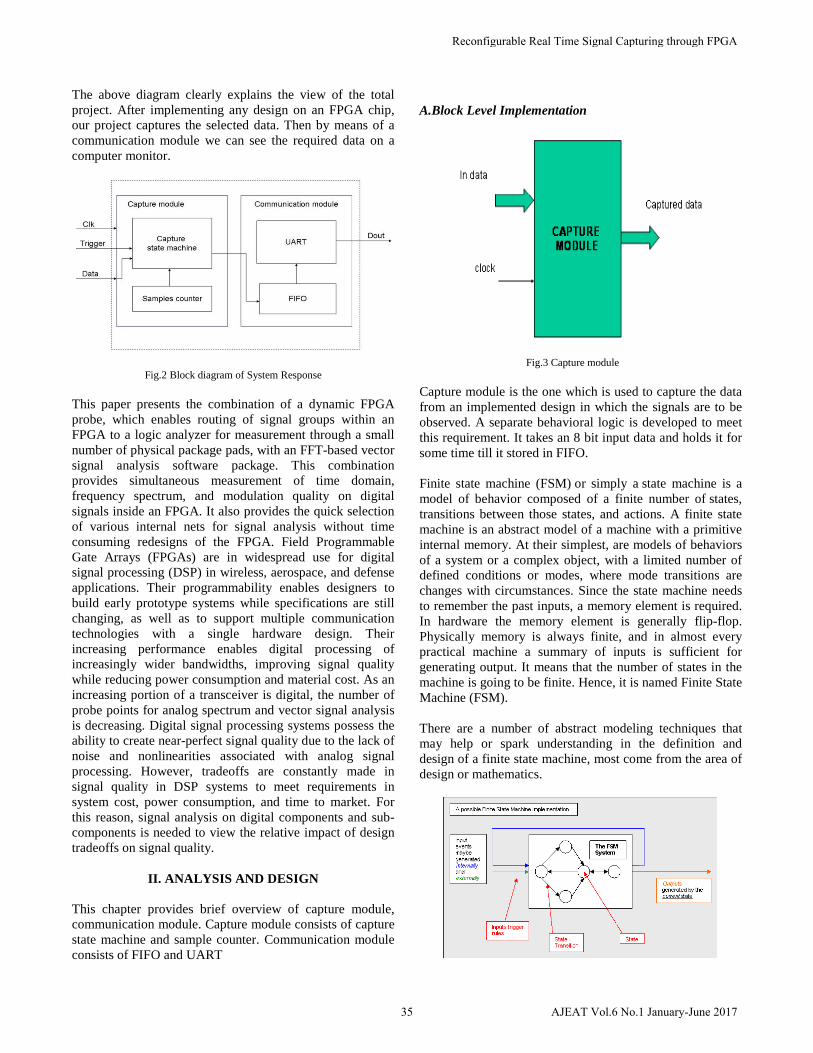
A.Block Level Implementation
Fig.3 Capture module
Capture module is the one which is used to capture the data from an implemented design in which the signals are to be observed. A separate behavioral logic is developed to meet this requirement. It takes an 8 bit input data and holds it for some time till it stored in FIFO. Finite state machine (FSM) or simply a state machine is a model of behavior composed of a finite number of states, transitions between those states, and actions. A finite state machine is an abstract model of a machine with a primitive internal memory. At their simplest, are models of behaviors of a system or a complex object, with a limited number of defined conditions or modes, where mode transitions are changes with circumstances. Since the state machine needs to remember the past inputs, a memory element is required. In hardware the memory element is generally flip-flop. Physically memory is always finite, and in almost every practical machine a summary of inputs is sufficient for generating output. It means that the number of states in the machine is going to be finite. Hence, it is named Finite State Machine (FSM). There are a number of abstract modeling techniques that may help or spark understanding in the definition and design of a finite state machine, most come from the area of design or mathematics.
35 AJEAT Vol.6 No.1 January-June 2017
Reconfigurable Real Time Signal Capturing through FPGA

Fig.4 A possible FSM-CS implementation
Hierarchical Task Analysis (HTA): Though it does not look at states, HTA is a task decomposition technique that looks at the way a task can be split into subtask, and the order in which they are performed.
B.Asynchronous FIFO Design
Fig.5 FIFO read & write pointers.
FIFO is an acronym for First In, First Out. FIFO is a memory element and also provides synchronization between the input and output data. To reach this requirement of synchronization we need a separate mechanism. In general writing into FIFO and reading from the FIFO may be of different speeds namely W-CLK and R-CLK respectively. We are implementing the FIFO with a special architecture according to the requirement. This expression describes the principle of a queue processing technique or servicing conflicting demands by ordering process by first-come, first-served (FCFS) behavior: what comes in first is handled first, what comes in next waits until the first is finished, etc. Thus it is analogous to the behavior of persons queuing where the persons leave the queue in the order they arrive, or waiting one's turn at a traffic control signal. For FIFOs of non-trivial size a dual-port SRAM is usually used where one port is used for writing and the other is used for reading. A synchronous FIFO is a FIFO where the same clock is used for both reading and writing. An asynchronous FIFO uses different clocks for reading and writing. Asynchronous FIFOs introduce metastability issues. Common implementation of an asynchronous FIFO uses a Gray code (or any unit distance code) for the read and writes pointers to ensure reliable flag generation.
C. Asynchronous FIFO Pointers In order to understand FIFO design, one needs to understand how the FIFO pointers work. The write pointer always points to the next word to be written; therefore, on reset, both pointers are set to zero, which also happens to be the next FIFO word location to be written. On a FIFO-write operation, the memory location that is pointed to by the write pointer is written, and then the write pointer is incremented to point to the next location to be written. Similarly, the read pointer always points to the current FIFO
word to be read. Again on reset, both pointers are reset to zero, the FIFO is empty and the read pointer is pointing to invalid data because the FIFO is empty and the empty flag is asserted. As soon as the first data word is written to the FIFO, the write pointer increments, the empty flag is cleared, and the read pointer that is still addressing the contents of the first FIFO memory word, immediately drives word, the receiver would clock once to output the data word from the FIFO, and clock a second time to capture the data word into the receiver. That would be needlessly inefficient. The FIFO is empty when the read and write pointers are both equal. This condition happens when both pointers are reset to zero during a reset operation, or when the read pointer catches up to the write pointer, having read the last word from the FIFO. That first valid word onto the FIFO data output port, to be read by the receiver logic. The fact that the read pointer is always pointing to the next FIFO word to be read means that the receiver logic does not have to use two clock periods to read the data word. A FIFO is full when the pointers are again equal, that is, when the write pointer has wrapped around and caught up to the read pointer. This is a problem. The FIFO is either empty or full when the pointers are equal, but which? One design technique used to distinguish between full and empty is to add an extra bit to each pointer. When the write pointer increments previous final FIFO address, the write pointer will increment the unused MSB while setting the rest of the bits back to zero as shown in Fig2.4.The same is done with the read pointer. If the MSBs of the two pointers are different, it means that the write pointer has wrapped one more time that the read pointer. If the MSBs of the two pointers are the same, it means that two pointers have wrapped the same number of times. Using n-bit pointers where (n-1) is the number of address bits required to access the entire FIFO memory buffer; the FIFO is empty when both pointers, including the MSBs are equal. And the FIFO is full when both pointers, except MSBs are equal. The FIFO design uses n-bit pointers for a FIFO with 2(n-1) write-able locations to help handle full and empty conditions.
36AJEAT Vol.6 No.1 January-June 2017
B.H.K Bhagat Kumar and S Khadar Bhasha

Fig.6 Block diagram for FIFO
III. BINARY FIFO CONSIDERATIONS Trying to synchronize a binary count value from one clock domain to another is problematic because every bit of an n-bit counter can change simultaneously for example 7->8 in binary numbers is 0111->1000, all bits changed. One approach to the problem is sample and hold periodic binary count values in a holding register and pass a synchronized ready signal to the new clock domain. When the ready signal is recognized, the receiving clock domain sends back a synchronized acknowledge signal to the sending Clock domain. A sampled pointer must not change until an acknowledge signal is received from the receiving clock domain. A count-value with multiple changing bits can be safely transferred to a new clock domain using this technique. Upon receipt of an acknowledge signal, the sending clock domain has permission to clear the ready signal and re-sample the binary count value.
Fig.7 FIFO full and empty conditions
Using this technique, the binary counter values are sampled periodically and not the entire binary counter values can be passed to a new clock domain. The question is, do we need to be concerned about the case where a binary counter might continue to increment and overflow or underflow the FIFO between sampled counter values? The answer is no FIFO full occurs when the write pointer catches up to the synchronized and sampled read pointer. The synchronized and sampled read pointer might not reflect the current value of the actual read pointer but the write pointer will not try to count beyond the synchronized read pointer value. Overflow will not occur .FIFO empty occurs when the read pointer catches up to the synchronized and sampled write pointer. The synchronized and sampled write pointer might not reflect the current value of the actual write pointer but the read pointer will not try to count beyond the synchronized write pointer value. Underflow will not occur
.A common approach to FIFO counter-pointers is to use Gray code counters. Gray codes only allow one bit to change for each clock transition, eliminating the problem associated with trying to synchronize multiple changing signals on the same clock edge. A.Handling Full & Empty Conditions Exactly how FIFO full and FIFO empty are implemented is design-dependent. In the FIFO design , assumes that the empty flag will be generated in the read-clock domain to insure that the empty flag is detected immediately when the FIFO buffer is empty, that is, the instant that the read pointer catches up to the write pointer (including the pointer MSBs). Similarly assumes that the full flag will be generated in the write-clock domain to insure that the full flag is detected immediately when the FIFO buffer is full, that is, the instant that the write pointer catches up to the read pointer (except for different pointer MSBs). B.Generating Empty As shown in Figure 3.5, the FIFO is empty when the read pointer and the synchronized write pointer are equal. The empty comparison is simple to do. Pointers that are one bit larger than needed to address the FIFO memory buffer are used. If the extra bits of both pointers (the MSBs of the pointers) are equal, the pointers have wrapped the same number of times and if the rest of the read pointer equals the synchronized write pointer, the FIFO is empty. C.Generating Full The full comparison is not as simple to do as the empty comparison. Pointers that are one bit larger than needed to address the FIFO memory buffer are still used for the comparison, but simply using Gray code counters with an extra bit to do the comparison is not valid to determine the full condition. The problem is that a Gray code is a symmetric code except for the MSBs.
IV. UART This provides brief overview of communication block and its components UART, timer block, multiplexer. The Universal Asynchronous Receiver/Transmitter (UART) controller is the key component of the serial communications subsystem of a computer. The UART takes bytes of data and transmits the individual bits in a sequential fashion. Serial transmission of digital information (bits) through a single wire or other medium is much more cost effective than parallel transmission through multiple wires. The primary functions of the UART are to perform serial-to-parallel and parallel-to-serial conversion of data and to perform error detection by inserting & checking parity bits and to insert & detect start and stop bits.
37 AJEAT Vol.6 No.1 January-June 2017
Reconfigurable Real Time Signal Capturing through FPGA
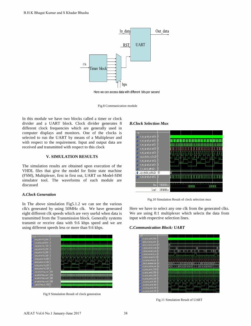
Fig.8 Communication module
In this module we have two blocks called a timer or clock divider and a UART block. Clock divider generates 8 different clock frequencies which are generally used in computer displays and monitors. One of the clocks is selected to run the UART by means of a Multiplexer and with respect to the requirement. Input and output data are received and transmitted with respect to this clock
V. SIMULATION RESULTS The simulation results are obtained upon execution of the VHDL files that give the model for finite state machine (FSM), Multiplexer, first in first out, UART on Model-SIM simulator tool. The waveforms of each module are discussed A.Clock Generation
In The above simulation Fig5.1.2 we can see the various clk's generated by using 50MHz clk. We have generated eight different clk speeds which are very useful when data is transmitted from the Transmission block. Generally systems transmit or receive data with 9.6 kbps speed and we are using different speeds less or more than 9.6 kbps.
Fig.9 Simulation Result of clock generation
B.Clock Selection Mux
Fig.10 Simulation Result of clock selection mux Here we have to select any one clk from the generated clks. We are using 8:1 multiplexer which selects the data from input with respective selection lines. C.Communication Block: UART
Fig.11 Simulation Result of UART
38AJEAT Vol.6 No.1 January-June 2017
B.H.K Bhagat Kumar and S Khadar Bhasha
D.Top level RSC
The following figure 5.4 gives the wave form that depicts the performance of Top level RSC.
Fig.12 Simulation Result of Top module
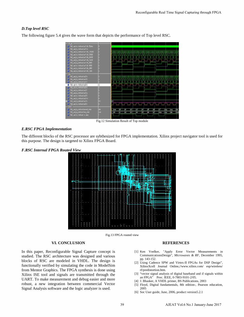
E.RSC FPGA Implementation
The different blocks of the RSC processor are sybthesized for FPGA implementation. Xilinx project navigator tool is used for this purpose. The design is targeted to Xilinx FPGA Board. F.RSC Internal FPGA Routed View
Fig.13 FPGA routed view
VI. CONCLUSION
In this paper, Reconfigurable Signal Capture concept is studied. The RSC architecture was designed and various blocks of RSC are modeled in VHDL. The design is functionally verified by simulating the code in ModelSim from Mentor Graphics. The FPGA synthesis is done using Xilinx ISE tool and signals are transmitted through the UART. To make measurement and debug easier and more robust, a new integration between commercial Vector Signal Analysis software and the logic analyzer is used.
REFERENCES
[1] Ken Voelker, "Apply Error Vector Measurements in CommunicationsDesign", Microwaves & RF, December 1995, pp. 143-152.
[2] Using Cadence SPW and Virtex-II FPGAs for DSP Design”, XilinxXcell Journal Online,//www.xilinx.com/ esp/wireless/ rf/predistortion.htm.
[3] “vector signal analysis of digital baseband and if signals within an FPGA” Proc. IEEE, 0-7803-9101-2/05.
[4] J. Bhasker, A VHDL primer, BS Publications, 2003 [5] Floyd, Digital fundamentals, 8th edition-, Pearson education,
2005 [6] Soc User guide, June, 2006, product version5.2.1
39 AJEAT Vol.6 No.1 January-June 2017
Reconfigurable Real Time Signal Capturing through FPGA