recent developments in device reliability … developments in device reliability modeling: the bias...
TRANSCRIPT

Recent Developments in
Device Reliability Modeling:
The Bias Temperature Instability
Tibor Grasser
Institute for Microelectronics, TU ViennaGußhausstraße 27–29, A-1040 Wien, Austria
TU Wien, Vienna, Austria

1/37
The Negative Bias Temperature InstabilityThe Negative Bias Temperature Instability
Huard et al., MR ’06
Negative bias temperature stress of pMOSFETs[1] [2] [3]
Large negative gate voltage (≈ 5 − 8 MV/cm), all other terminals grounded
Elevated temperatures (typically 100 ◦C– 200 ◦C, but also at room temperature)
Degradation of critical device parametersThreshold voltage
Subthreshold slope
Transconductance
Mobility
Drain current
...
Occurs in all four configurationsStrongest in pMOS with negative bias
Serious reliability concern in pMOSFETs[1]
Schroder and Babcock, JAP ’03[2]
Alam and Mahapatra, MR ’05[3]
Huard et al., MR ’06

2/37
The Negative Bias Temperature InstabilityThe Negative Bias Temperature Instability
When does the NBTI scenario occur?NBTI: VG ≪ 0 V, VS = VD = 0 V
Example: inverter with Vin = 0 V
Similar scenarios in ring-oscillators, SRAM cells, etc.
VDD
Vin Vout
What happens to the pMOS transistor?
Kimizuka et al., VLSI Symp. ’00
3/37
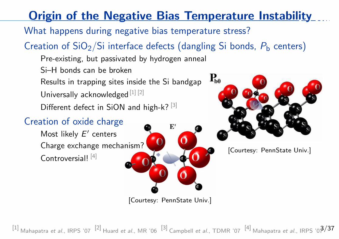
Origin of the Negative Bias Temperature InstabilityOrigin of the Negative Bias Temperature Instability
[Courtesy: PennState Univ.]
[Courtesy: PennState Univ.]
What happens during negative bias temperature stress?
Creation of SiO2/Si interface defects (dangling Si bonds, Pb centers)Pre-existing, but passivated by hydrogen anneal
Si–H bonds can be broken
Results in trapping sites inside the Si bandgap
Universally acknowledged [1] [2]
Different defect in SiON and high-k? [3]
Creation of oxide chargeMost likely E ′ centers
Charge exchange mechanism?
Controversial! [4]
[1]Mahapatra et al., IRPS ’07
[2]Huard et al., MR ’06
[3]Campbell et al., TDMR ’07
[4]Mahapatra et al., IRPS ’07

4/37
NBTI Measurement TechniquesNBTI Measurement Techniques
Main problem: it is impossible to perfectly measure NBTI
As soon as stress is removed, extremely fast recovery is observed [1] [2]
Strong bias dependence, in particular to positive bias [3] [4] [5]
A number of techniques have been suggest and used
Conventional Measure/Stress/Measure [6]
On-the-fly (during stress, no interruption) [7]
Charge-pumping and DCIV techniques [8]
Various problemsDelays lead to recovery
How to quantify the degradation (∆Vth, ∆ID, ???)
Biggest problem: results do not match!!!No exact theory available that unanimously links and explains all the data
[1]Ershov et al., IRPS ’03
[2]Reisinger et al., IRPS ’06
[3]Ang, EDL ’06
[4]Huard et al., MR ’06
[5]Grasser et al., IEDM ’07
[6]Kaczer et al., IRPS ’05
[7]Denais et al., IEDM ’04
[8]Neugroschel et al., IEDM ’06

5/37
Influence of DelayInfluence of Delay
Measurement delay has a significant impact on measurement[1] [2] [3]
Curvature in data becomes more obvious, larger (time-dependent) ’slope’
Impact of delay does not disappear at longer stress times
Impact of delay is temperature dependent
100
101
102
103
104
105
Net Stress Time [s]
10
100
∆Vth
[m
V]
200oC
125oC
50oC
10 ms10 s10 ms10 s
10 ms
10 s
10-2
10-1
100
101
Delay Time [s]
0.12
0.14
0.16
0.18
0.2
Eff
ectiv
e Po
wer
Law
Slo
pe
200oC
150oC
100oC
50oC
[1]Ershov et al., IRPS ’03
[2]Denais et al., IEDM ’04
[3]Kaczer et al., IRPS ’05
6/37
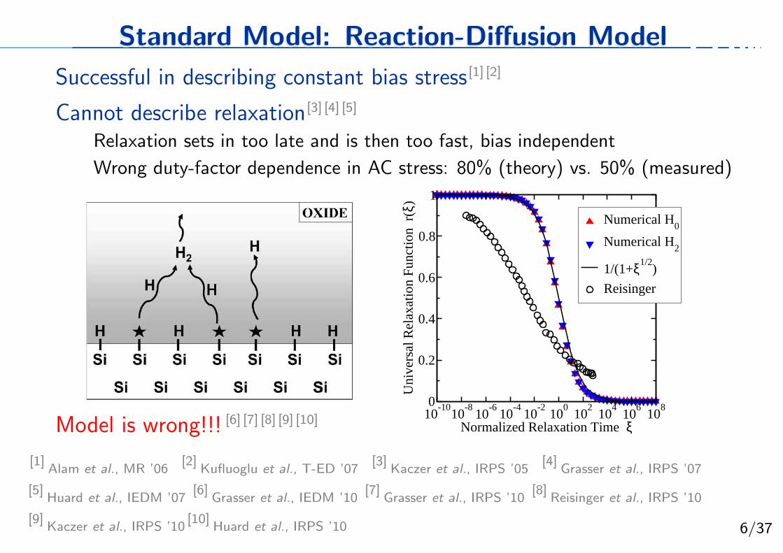
Standard Model: Reaction-Diffusion ModelStandard Model: Reaction-Diffusion Model
Successful in describing constant bias stress [1] [2]
Cannot describe relaxation[3] [4] [5]
Relaxation sets in too late and is then too fast, bias independent
Wrong duty-factor dependence in AC stress: 80% (theory) vs. 50% (measured)
10-10
10-8
10-6
10-4
10-2
100
102
104
106
108
Normalized Relaxation Time ξ
0
0.2
0.4
0.6
0.8
1
Uni
vers
al R
elax
atio
n Fu
nctio
n r
(ξ)
Numerical H0
Numerical H2
1/(1+ξ1/2)
Reisinger
Model is wrong!!! [6] [7] [8] [9] [10]
[1]Alam et al., MR ’06
[2]Kufluoglu et al., T-ED ’07
[3]Kaczer et al., IRPS ’05
[4]Grasser et al., IRPS ’07
[5]Huard et al., IEDM ’07
[6]Grasser et al., IEDM ’10
[7]Grasser et al., IRPS ’10
[8]Reisinger et al., IRPS ’10
[9]Kaczer et al., IRPS ’10
[10]Huard et al., IRPS ’10
7/37
OverviewOverview
IntroductionStochastic NBTI on small-area devices: link NBTI and RTN
New measurement techniqueThe time dependent defect spectroscopy
Anomalous defect behaviorPresent in all defects
Stochastic modelAdditional metastable states, multiphonon theory
Compact modeling attemptRC ladders
Implications on lifetimes
Conclusions
8/37
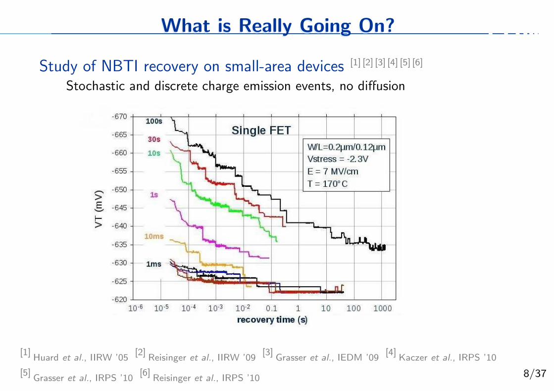
What is Really Going On?What is Really Going On?
Study of NBTI recovery on small-area devices [1] [2] [3] [4] [5] [6]
Stochastic and discrete charge emission events, no diffusion
[1]Huard et al., IIRW ’05
[2]Reisinger et al., IIRW ’09
[3]Grasser et al., IEDM ’09
[4]Kaczer et al., IRPS ’10
[5]Grasser et al., IRPS ’10
[6]Reisinger et al., IRPS ’10

9/37
Recoverable NBTI due to the same Defects as RTNRecoverable NBTI due to the same Defects as RTN
Quasi-equilibrium:Some defects neutral, others positive, a few produce random telegraph noise (RTN)
Stress:Defects switch to new equilibrium (mostly positive), a few may produce RTN
Recovery:Slow transition (broad distribution of timescales) to initial quasi-equilibrium
0 200 400 600 800 1000Time [s]
Sum
#11
#10
#8
#4
#3
+
0
Equilibrium: RTN
VG = -0.5V
10-6
10-5
10-4
10-3
10-2
10-1
100
101
102
103
Charging Time [s]
Non-Equilibrium: Charging
VG = -1.8V
10-6
10-5
10-4
10-3
10-2
10-1
100
101
102
103
104
Discharging Time [s]
EquilibriumRTN
Non-Equilibrium: Discharging
VG = -0.5V

10/37
The Time Dependent Defect Spectroscopy (TDDS)The Time Dependent Defect Spectroscopy (TDDS)
Analyzes contributions from multiple traps via spectral maps [1] [2]
0
5
10∆V
th [
mV
]
10-5
10-4
10-3
10-2
10-1
100
101
102
Emission Time [s]
0
2
4
6
Ste
p H
eigh
t [m
V]
ts = 1msT = 100
oC
VG = -1.7V
Time Domain
[1]Grasser et al., IRPS ’10
[2]For a discussion on the step heights see Kaczer et al., IRPS ’10

10/37
The Time Dependent Defect Spectroscopy (TDDS)The Time Dependent Defect Spectroscopy (TDDS)
Analyzes contributions from multiple traps via spectral maps
0
5
10∆V
th [
mV
]
10-5
10-4
10-3
10-2
10-1
100
101
102
Emission Time [s]
0
2
4
6
Ste
p H
eigh
t [m
V]
Spectrum
ts = 1msT = 100
oC
VG = -1.7V
Time Domain
[0] [0]

10/37
The Time Dependent Defect Spectroscopy (TDDS)The Time Dependent Defect Spectroscopy (TDDS)
Analyzes contributions from multiple traps via spectral maps
0
5
10∆V
th [
mV
]
10-5
10-4
10-3
10-2
10-1
100
101
102
Emission Time [s]
0
2
4
6
Ste
p H
eigh
t [m
V]
Spectrum
#3
#4
#1
#2
#12
#3
#4
#1
#2
#12
#3
#4
#1
#2
#12 ts = 1msT = 100
oC
VG = -1.7V
Time Domain
[0] [0]

11/37
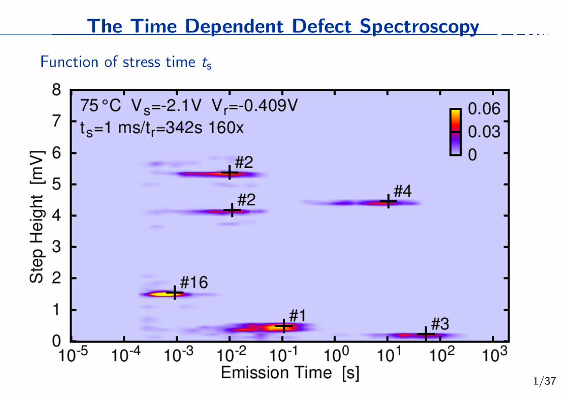
The Time Dependent Defect SpectroscopyThe Time Dependent Defect Spectroscopy
Function of stress time ts

11/37
The Time Dependent Defect SpectroscopyThe Time Dependent Defect Spectroscopy
Function of stress time ts
11/37
The Time Dependent Defect SpectroscopyThe Time Dependent Defect Spectroscopy
Function of stress time ts

11/37
The Time Dependent Defect SpectroscopyThe Time Dependent Defect Spectroscopy
Function of stress time ts

12/37
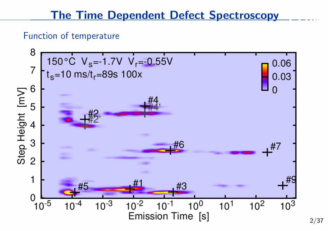
The Time Dependent Defect SpectroscopyThe Time Dependent Defect Spectroscopy
Function of temperature

12/37
The Time Dependent Defect SpectroscopyThe Time Dependent Defect Spectroscopy
Function of temperature
12/37
The Time Dependent Defect SpectroscopyThe Time Dependent Defect Spectroscopy
Function of temperature

12/37
The Time Dependent Defect SpectroscopyThe Time Dependent Defect Spectroscopy
Function of temperature

13/37
The Time Dependent Defect SpectroscopyThe Time Dependent Defect Spectroscopy
Different non-linear field dependence of the capture time constants
Different bias dependence of emission time constant: two defect types?
0.5 1 1.5 2 2.5 -VG [V]
10-7
10-6
10-5
10-4
10-3
10-2
10-1
100
101
102
103
Cap
ture
Tim
e C
onst
ant
[s]
#1 125oC
#3 125oC
#4 125oC
#6 125oC
#8 125oC
tRTN: τcs 125
oC
#1 175oC
#3 175oC
#4 175oC
#8 175oC
#10 175oC
#11 175oC
tRTN: τcs 175
oC
~1/ID
VthVDD
10-4
10-3
10-2
10-1
100
#2 (lin/125oC)
#4 (lin/125oC)
#4 (lin/175oC)
#1 (sat/125oC)
#2 (sat/125oC)
#4 (sat/125oC)
0.2 0.4 0.6 0.8 1 1.2Negative Readout Voltage (-VG) [V]
10-4
10-3
10-2
10-1
100
101
E
mis
sion
Tim
e C
onst
ant
[s]
#1 (lin/125oC)
#3 (lin/125oC)
#1 (lin/175oC)
#3 (lin/175oC)
#3 (sat/125oC)
#6 (sat/125oC)
ID
Disappearing Switching Traps
Compare SRH-like model: τc = τ0 eβ∆EBNv
pτe = τ0 eβ∆EB eβ∆ET exF/VT

14/37
Anomalous Defect BehaviorAnomalous Defect BehaviorDefects disappear temporarily from the map (#7)
Long term stability: defect #6 missing for a few months now

15/37
Anomalous Defect BehaviorAnomalous Defect Behavior
Temporary random telegraph noise (tRTN)
0 2 4 6 8 10 12 14 16 18Relaxation Time [ms]
0
5
10
15
0
5
10
15
-∆V
th [
mV
]
0
5
10
15
Trace 23
Trace 16
Trace 14
T = 150oC / ts = 1s / Vs = -1.7V
#1 #4
#4#1
#14
#1
#4
No ModulationModulation
0 2 4 6 8 10 12 14 16 18Relaxation Time [ms]
0
5
10
15
0
5
10
15
-∆V
th [
mV
]
0
5
10
15T = 125
oC / ts = 100ms / Vs = -1.5VVr = -0.668V
Vr = -0.556V
Vr = -0.459V

16/37
Tewksbury ModelTewksbury Model
Tewksbury model[1]: charging and discharging of traps via elastic tunnelingEquilibrium Stress Recovery
[1]Tewksbury and Lee, SSC ’94

17/37
How Can We Model All That Properly?

18/37
Standard Model for RTNStandard Model for RTN
Model suggested by Kirton & Uren[1]
Noticed that elastic tunneling cannot be ’it’
Also used lattice-relaxation multiphonon emission (LRME)
Time constants depend on activation energy ∆EB and depth x
τc = τ0 eβ∆EBNv
pτ−10 = Nv vth σ e−x/x0
τe = τ0 eβ∆EB eβ∆ET exF/VT
B
Neutral DefectPrecursor Hole Capture
A
Standard Charge Capture/Emission Model
Charged TrapPositive Defect
Hole Emission
Kirton/Uren Model
LRME
LRME
+
[1]Kirton & Uren, Adv.Phys ’89
19/37
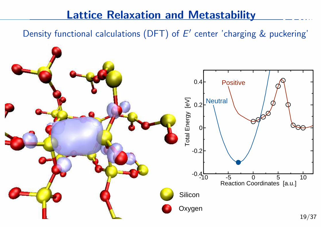
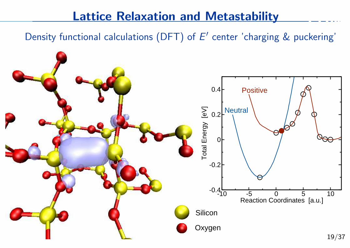
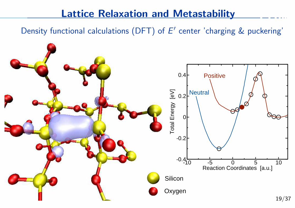
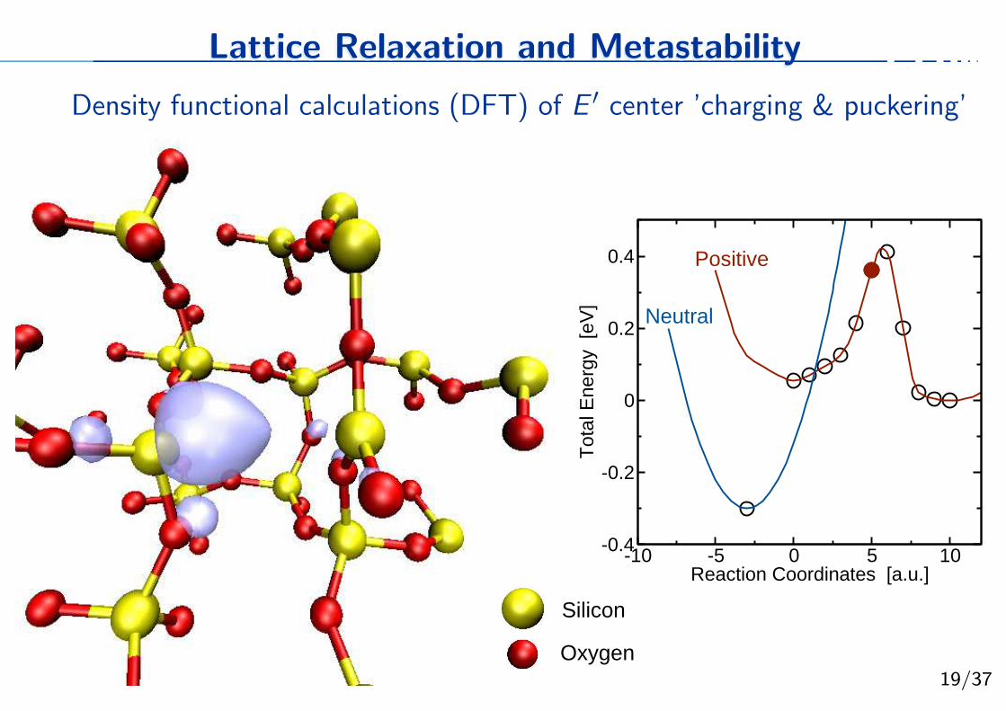
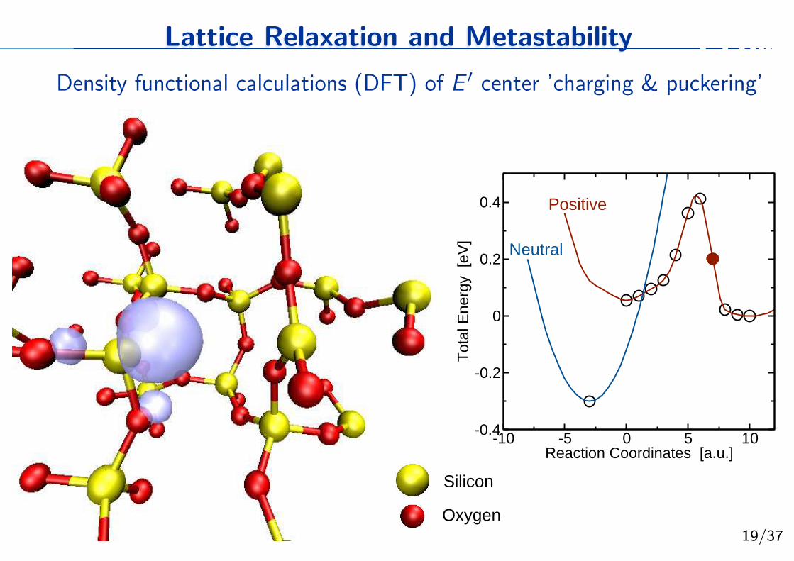
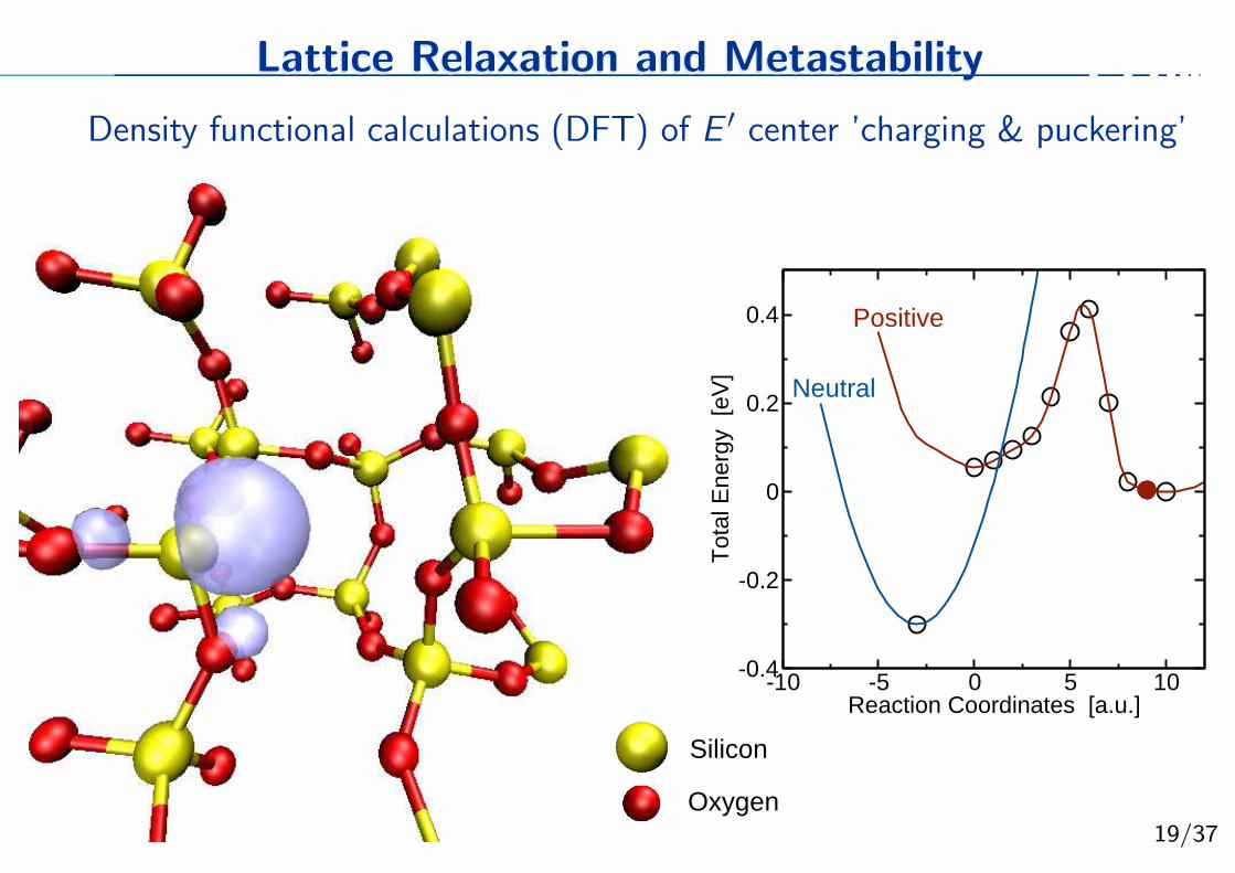
Lattice Relaxation and MetastabilityLattice Relaxation and Metastability
Density functional calculations (DFT) of E′ center ’charging & puckering’
-10 -5 0 5 10Reaction Coordinates [a.u.]
-0.4
-0.2
0
0.2
0.4
Tot
al E
nerg
y [e
V]
Positive
Neutral
Silicon
Oxygen

19/37
Lattice Relaxation and MetastabilityLattice Relaxation and Metastability
Density functional calculations (DFT) of E′ center ’charging & puckering’
-10 -5 0 5 10Reaction Coordinates [a.u.]
-0.4
-0.2
0
0.2
0.4
Tot
al E
nerg
y [e
V]
Positive
Neutral
Silicon
Oxygen
19/37
Lattice Relaxation and MetastabilityLattice Relaxation and Metastability
Density functional calculations (DFT) of E′ center ’charging & puckering’
-10 -5 0 5 10Reaction Coordinates [a.u.]
-0.4
-0.2
0
0.2
0.4
Tot
al E
nerg
y [e
V]
Positive
Neutral
Silicon
Oxygen
19/37
Lattice Relaxation and MetastabilityLattice Relaxation and Metastability
Density functional calculations (DFT) of E′ center ’charging & puckering’
-10 -5 0 5 10Reaction Coordinates [a.u.]
-0.4
-0.2
0
0.2
0.4
Tot
al E
nerg
y [e
V]
Positive
Neutral
Silicon
Oxygen

19/37
Lattice Relaxation and MetastabilityLattice Relaxation and Metastability
Density functional calculations (DFT) of E′ center ’charging & puckering’
-10 -5 0 5 10Reaction Coordinates [a.u.]
-0.4
-0.2
0
0.2
0.4
Tot
al E
nerg
y [e
V]
Positive
Neutral
Silicon
Oxygen

19/37
Lattice Relaxation and MetastabilityLattice Relaxation and Metastability
Density functional calculations (DFT) of E′ center ’charging & puckering’
-10 -5 0 5 10Reaction Coordinates [a.u.]
-0.4
-0.2
0
0.2
0.4
Tot
al E
nerg
y [e
V]
Positive
Neutral
Silicon
Oxygen
19/37
Lattice Relaxation and MetastabilityLattice Relaxation and Metastability
Density functional calculations (DFT) of E′ center ’charging & puckering’
-10 -5 0 5 10Reaction Coordinates [a.u.]
-0.4
-0.2
0
0.2
0.4
Tot
al E
nerg
y [e
V]
Positive
Neutral
Silicon
Oxygen

19/37
Lattice Relaxation and MetastabilityLattice Relaxation and Metastability
Density functional calculations (DFT) of E′ center ’charging & puckering’
-10 -5 0 5 10Reaction Coordinates [a.u.]
-0.4
-0.2
0
0.2
0.4
Tot
al E
nerg
y [e
V]
Positive
Neutral
Silicon
Oxygen
19/37
Lattice Relaxation and MetastabilityLattice Relaxation and Metastability
Density functional calculations (DFT) of E′ center ’charging & puckering’
-10 -5 0 5 10Reaction Coordinates [a.u.]
-0.4
-0.2
0
0.2
0.4
Tot
al E
nerg
y [e
V]
Positive
Neutral
Silicon
Oxygen

19/37
Lattice Relaxation and MetastabilityLattice Relaxation and Metastability
Density functional calculations (DFT) of E′ center ’charging & puckering’
-10 -5 0 5 10Reaction Coordinates [a.u.]
-0.4
-0.2
0
0.2
0.4
Tot
al E
nerg
y [e
V]
Positive
Neutral
Silicon
Oxygen
19/37
Lattice Relaxation and MetastabilityLattice Relaxation and Metastability
Density functional calculations (DFT) of E′ center ’charging & puckering’
-10 -5 0 5 10Reaction Coordinates [a.u.]
-0.4
-0.2
0
0.2
0.4
Tot
al E
nerg
y [e
V]
Positive
Neutral
Silicon
Oxygen

19/37
Lattice Relaxation and MetastabilityLattice Relaxation and Metastability
Density functional calculations (DFT) of E′ center ’charging & puckering’
-10 -5 0 5 10Reaction Coordinates [a.u.]
-0.4
-0.2
0
0.2
0.4
Tot
al E
nerg
y [e
V]
Positive
Neutral
Silicon
Oxygen

20/37
Detailed Defect Model RequiredDetailed Defect Model Required
Substratewith
ExchangeCharge
1 2
RelaxationStructural
NeutralStable
2’
PositiveMetastable
1’
NeutralMetastable
RelaxationStructural
Substratewith
ExchangeCharge
PositiveStable
+
+

21/37
ModelModel
Different adiabatic potentials for the neutral and positive defect
Metastable states 2’ and 1’ are secondary minimaThermal transitions to ground states 1 and 2
Stochastic Markov-model for defect kinetics based on multiphonon theory
-4 0 4 8 12Reaction Coordinates [a.u.]
-1
-0.5
0
0.5
1
1.5
2
2.5
Latti
ce +
Ele
ctro
nic
Ene
rgy
- E
V [
eV]
1
2’
2 1
Stress
EV
EC
1’
+
+

22/37
Qualitative Model EvaluationQualitative Model Evaluation
Normal random telegraph noise (RTN)Very similar energetical position of the minimas 1 and 2
0
1
f 2 (+
)
0
1
f 1’ (
Neu
tral
)
1 2 3 4Time [s]
0
1
f 1 (N
eutr
al)
-1 0 1 2 3 4 5 6 7 8 9Reaction Coordinates [a.u.]
0
0.5
1
1.5
2
Latti
ce +
Ele
ctro
nic
Ene
rgy
- E
V [
eV]
❏1❏2’
❏2❏1’
Kirton and Uren, Adv. Phys. ’89

23/37
Qualitative Model EvaluationQualitative Model Evaluation
Anomalous RTNVery similar energetical position of the three minima 1, 2, and 1’
0
1
f 2 (+
)
0
1
f 1’ (
Neu
tral
)
0 10 20 30 40 50 60Time [s]
0
1
f 1 (N
eutr
al)
-1 0 1 2 3 4 5 6 7 8 9Reaction Coordinates [a.u.]
0
0.5
1
1.5
2
Latti
ce +
Ele
ctro
nic
Ene
rgy
- E
V [
eV]
❏1❏2’
❏2 ❏1’
Uren et al., PRB ’88
24/37
Qualitative Model EvaluationQualitative Model Evaluation
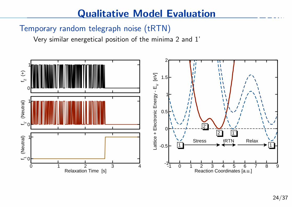
Temporary random telegraph noise (tRTN)Very similar energetical position of the minima 2 and 1’
0
1
f 2 (+
)
0
1
f 1’ (
Neu
tral
)
0 1 2 3 4Relaxation Time [s]
0
1
f 1 (N
eutr
al)
-1 0 1 2 3 4 5 6 7 8 9Reaction Coordinates [a.u.]
-1
-0.5
0
0.5
1
1.5
2
Latti
ce +
Ele
ctro
nic
Ene
rgy
- E
V [
eV]
❏1
❏2’
❏2 ❏1’
❏1Stress tRTN Relax

25/37
Quantitative Model EvaluationQuantitative Model Evaluation
Excellent agreement for both capture and emission time constantsCapture time: particularly important for back-extrapolation of stress data
Emission time: determines recovery behavior
Does the defect act like a switching trap?Depends on the defect configuration
0 0.5 1 1.5 2 2.5 -VG [V]
10-7
10-6
10-5
10-4
10-3
10-2
10-1
100
101
102 τc @125
oC
τc @175oC
τe @125oC
τe @175oC
fp @125oC
fp @125oC
Defect #1
0 0.5 1 1.5 2 2.5 -VG [V]
10-6
10-5
10-4
10-3
10-2
10-1
100
101
102 τc @125
oC
τc @175oC
τe @125oC
τe @175oC
fp @125oC
fp @125oC
Defect #4

26/37
How to Model This with SPICE?
Ck1
Ld
V0
Va
1
Re
C2
Ck2
T
LR2
R1C

27/37
Compact ModelingCompact Modeling
First attempt: approximate multi-state model by two-state model[1] [2]
Try to capture the notoriously difficult dynamics first
Effective capture and emission time constants
Differential equation for a two-state modelCorresponds to an RC equivalent circuit
Two branches: charging vs. discharging
[1]Kaczer et al., IRPS ’10
[2]Reisinger et al., IRPS ’10
28/37
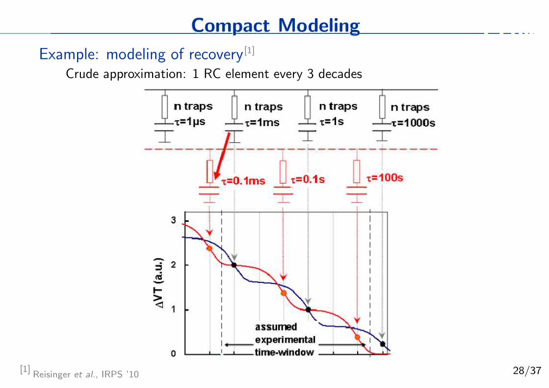
Compact ModelingCompact Modeling
Example: modeling of recovery[1]
Crude approximation: 1 RC element every 3 decades
[1]Reisinger et al., IRPS ’10

29/37
Compact ModelingCompact Modeling
Example: modeling of recovery[1]
Finer approximation: 2 RC elements every 3 decades
[1]Reisinger et al., IRPS ’10
30/37
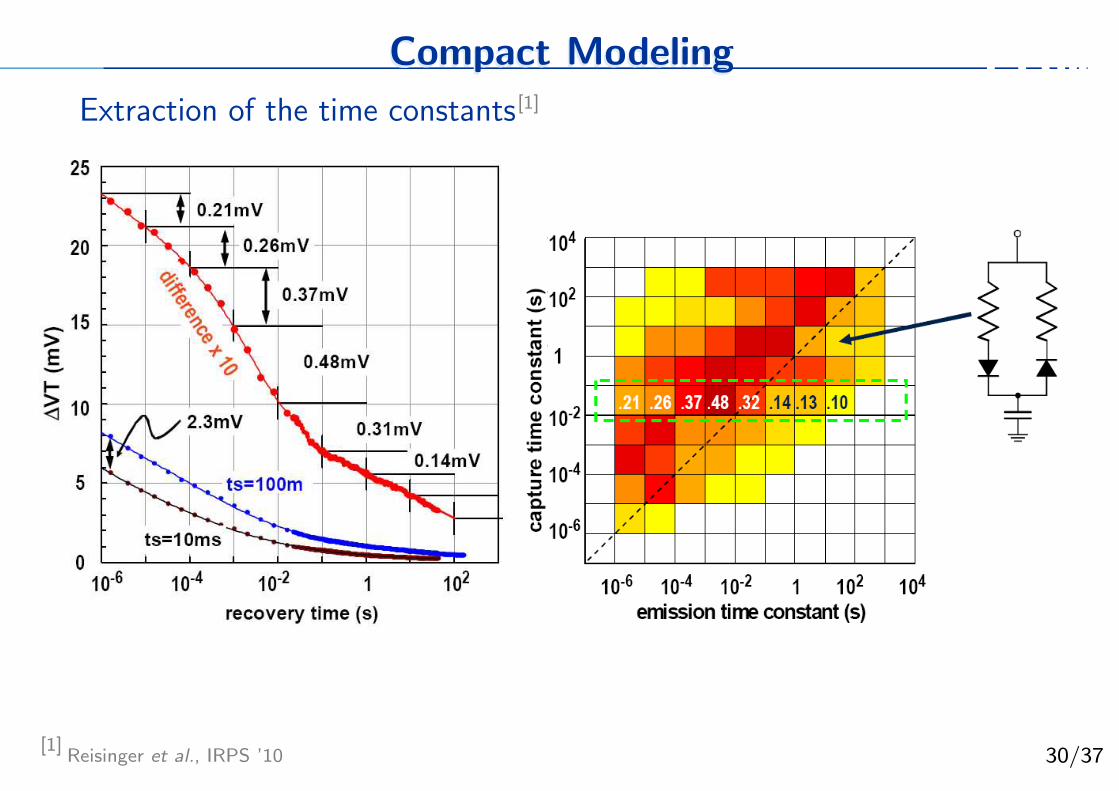
Compact ModelingCompact Modeling
Extraction of the time constants[1]
[1]Reisinger et al., IRPS ’10
31/37
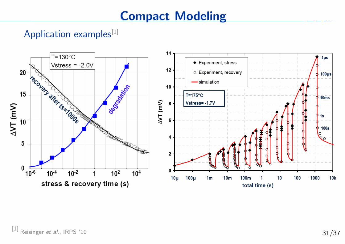
Compact ModelingCompact Modeling
Application examples[1]
[1]Reisinger et al., IRPS ’10

32/37
Compact ModelingCompact Modeling
Notorious: duty factor dependence[1] [2] [3]
[1]Grasser et al., IEDM ’07
[2]Grasser et al., IRPS Tutorial ’08
[3]Reisinger et al., IRPS ’10

33/37
Why Would We Care?
34/37
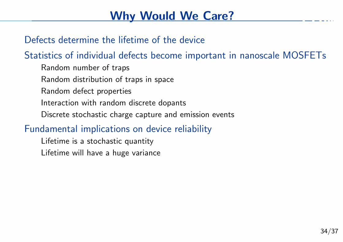
Why Would We Care?Why Would We Care?
Defects determine the lifetime of the device
Statistics of individual defects become important in nanoscale MOSFETsRandom number of traps
Random distribution of traps in space
Random defect properties
Interaction with random discrete dopants
Discrete stochastic charge capture and emission events
Fundamental implications on device reliabilityLifetime is a stochastic quantity
Lifetime will have a huge variance

35/37
How to Determine the Lifetime?How to Determine the Lifetime?
Small area devices: lifetime is a stochastic quantity [1] [2]
Charge capture/emission stochastic events
Capture and emission times distributed
Number of defects follow Poisson distribution
For details see Grasser et al. IEDM ’10
[1]Kaczer et al. IRPS ’09
[2]Grasser et al. IEDM ’10

36/37
ConclusionsConclusions
NBTI/PBTI is a challenging problem to understand and model
Dynamics are of utmost importanceFor example: DC vs. AC stress, duty factor dependence, bias dependence, etc.
What happens in a circuit?
Cannot be captured by existing models
Measurement method: time dependent defect spectroscopy (TDDS)Operates on nanoscale MOSFETs with a handful of defects
Allows extraction of τe, τc, and step-height over very wide range
Allows simultaneous analysis of multiple defects
New defect modelMetastable defect states, nonradiative multiphonon theory, stochastic behavior
First attempts towards compact modelingEquivalent RC circuits which deliver ∆Vth
Can capture the main features, e.g. DC vs. AC
Lifetime becomes a stochastic quantity
37/37
This work would have been impossible without the support of ...This work would have been impossible without the support of ...
The Institute for MicroelectronicsE. Langer, S. Selberherr, ...
My Ph.D. students W. Gos, Ph. Hehenberger, F. Schanovsky, and P.-J. Wagner
B. Kaczer and G. Groeseneken (IMEC)
Longstanding collaboration, tons of measurement data, discussion/theory
M. Nelhiebel, Th. Aichinger, J. Fugger, and O. Haberlen (Infineon Villach)Financial support, measurement data, and discussion
R. Minixhofer and H. Enichlmair (austriamicrosystems)Financial support, measurement data, and discussion
H. Reisinger, C. Schlunder, and W. Gustin (Infineon Munich)
Ultra fast measurement data, discussion/theory
‘Reliability community’P. Lenahan, J. Campbell, G. Bersuker, V. Huard, N. Mielke, A.T. Krishnan, ...
Funding byEU FP7 contract n◦216436 (ATHENIS), ENIAC project n◦820379 (MODERN), CDG