real-time signal processing and hardware …€¦ · (fbg) and the long period grating (lpg)...
TRANSCRIPT
Real-Time Signal Processing and Hardware Development for a Wavelength
Modulated Optical Fiber Sensor System
by
Shah M. Musa
Dissertation submitted to the Faculty of the
Virginia Polytechnic Institute and State University
in partial fulfillment of the requirements for the degree of
Doctor of Philosophy
in
Electrical and Computer Engineering
Approved
Kent A. Murphy, Chair
Richard O. Claus
Jeffrey H. Reed
Roger L. Simpson
Anbo Wang
June 26, 1997
Blacksburg, Virginia
Keywords: Real-time DSP, optical fiber sensor, extrinsic Fabry-Perot interferometer, fiber Bragg
grating sensor
Copyright 1997, Shah M. Musa

ii
Real-Time Signal Processing and Hardware Development for a Wavelength
Modulated Optical Fiber Sensor System
by
Shah M. Musa
Kent A. Murphy, Chairman
The Bradley Department of Electrical and Computer Engineering, Virginia Tech
(ABSTRACT)
The use of optical fiber sensors is increasing widely in civil, industrial, and military applications
mainly due to their, (a) miniature size, (b) high sensitivity, (c) immunity from electro-magnetic
interference, (d) resistance to harsh environments, (e) remote signal processing ability, and, (f)
multiplexing capabilities. Because of these advantages a variety of optical fiber sensing
techniques have evolved over the years having potentials for myriad of applications. One very
challenging job, for any of these optical fiber sensing techniques, is to implement a stand alone
system with the design and development of all the signal processing models along with the
necessary hardware, firmware, and software satisfying the real-time signal processing
requirements. In this work we first develop the equations for the system model of the
wavelength modulated extrinsic Fabry-Perot interferometric (EFPI) optical fiber sensor, and then
design and build all the hardware and software necessary to implement a stand-alone system,
satisfying all the requirements of the real-time signal processing capabilities. We also present the
real-time system constructions and the signal processing techniques for the fiber Bragg grating
(FBG) and the long period grating (LPG) sensors, and develop all the necessary signal processing
software for the FBG system. The Texas Instruments TMS320C40 floating point digital signal
processing (DSP) chip is used as the mother processor for the system. All the hardware and
software necessary to interface the stand alone system to the Internet is also designed and
developed, and one can establish a client/server environment using the TCP/IP protocol suite to
acquire data, and/or monitor or control the system, using computers having Internet IP addresses
assigned to them.

iii
Acknowledgments
I would like to thank Dr. Kent Murphy, Dr. Richard Claus, Dr. Anbo Wang, Dr. Jeffrey Reed,
and Dr. Roger Simpson for serving on my committee and providing all the thoughtful
suggestions. It has been both a pleasure and an honor to work with all of them.
I would like to express my special gratitude and appreciation to Dr. Kent Murphy, for accepting
me to work with him as a graduate student, and for providing me with all the resources for this
work.
I am grateful to Tracy Cramer, who did the overall design of the ‘C40 board, William Cockey,
who did all the PCB layout for the boards, John Turman, who did all the populations for the
boards, Frank Greenley, who took all the pains to do all the signal tracings and corrections to
make the system work, and Paul Duncan, my mentor both in the hardware and the software
world, who made all the decisions, supervisions, and corrections all along the entire work. My
own contribution in the hardware part, were mainly in designing the analog-to-digital conversion
(ADC) board, designing the interfacing connections of the boards, and designing and developing
the Xilinx FPGAs for the ‘C40 board. I wish to thank Dr. Kevin Shinpaugh, Tracy Cramer, and
Steve Poland for providing me many of the real-time signal processing algorithms for this work.
I wish to thank all the people of F&S Inc., Blacksburg and of FEORC, Virginia Tech, for
providing me such an excellent research environment.
I am thankful to my parents and all my brothers and sisters for providing me support, morally and
financially, to come to Virginia Tech for graduate studies. I am greatly thankful to my wife Aliya
Shafquat, who herself being a full-time graduate student of Virginia Tech, managed to do all the
works of home and at the same time raise our newborn Zuhayeer Hammam Musa, who is only
eight months old now. And above all, I am thankful to Allah for providing me with all the
opportunities to work with this project and making it possible to complete it.

iv
Table of Contents
Chapter 1. Introduction…………………………………………………………………..1
1.1 Applications of Optical Fiber Sensors……………………………………………..1
1.2 Optical Fiber Sensing Techniques……………….………………………………..4
1.2 Wavelength Modulated Optical Fiber Sensors……………………….……………7
1.3 Objective and Scope……………………………………………………………….8
1.4 Organization of the Dissertation…………………………………………………..9
Chapter 2. The Wavelength Modulated EFPI Sensor System……………………….11
2.1 Construction of the Real-Time Wavelength Modulated EFPI Sensor System…..11
2.2 The System Signal Response…………………….………………………………13
2.3 Modeling the Wavelength Modulated EFPI Sensor System……………………..13
2.4 Demodulation Techniques of the Signal Response………………………………19
2.4.1 Peak-to-Peak Method…………………………………………………..19
2.4.2 FFT Method…………………………………………………………….23
2.4.3 Discrete Gap Transform Method……………………………………….25
2.4.4 FFT and then Discrete Gap Transform with Golden Search Rule……..27
Chapter 3. The FBG and The LPG Sensor Systems..…………………………………40
3.1 Construction and Signal Response of the FBG Sensor System…..………………40
3.2 Construction and Signal Response of the LPG Sensor System…………………..41
3.3 Fabrication of the FBG and the LPG Sensors……………………………………42
3.4 Principle of Operations of the FBG and the LPG Sensor Systems………………43
3.5 Demodulation Techniques for the Signal Response of the Real-Time
FBG Sensor System………………………………………………………………46
3.6 Demodulation Techniques for the Signal Response of the Real-Time
LPG Sensor System………………………………………………………………48
3.7 Summary of the FBG and the LPG Sensor Systems……………………………..48

v
Chapter 4. Hardware Development……………………………………………………54
4.1 S1000 Linear Array CCD Spectrometer………………………………………….54
4.2 Analog-to-Digital Conversion Board……………………………………………..55
4.3 TMS320C40 Board……………………………………………………………….56
4.4 Programming the Logic for the Xilinx FPGA XC4003A-4PC84………………..59
Chapter 5. Firmware and Software Development……………………………………..68
5.1 DSP Firmware and Software Development Environment………………………..68
5.2 Development of the DSP Firmware and Software……………………………….69
5.2.1 The Initialization Routines……………………………………………..70
5.2.2 The Data Acquisition Routine………………………………………….71
5.2.3 The UART Service Routine…………………………………………….72
5.2.4 The EFPI Signal Processing Routines………………………………….72
5.2.5 The FBG Signal Processing Routines………………………………….73
5.2.6 The Memory Allocation File…………………………………………..74
5.3 The TCP/IP Client/Server Software Development Environment………………..74
5.4 Development of the TCP/IP Client/Server Software…………………………….74
5.4.1 TCP/IP Client Programs……………………………………………….75
5.4.2 TCP/IP Server Programs……………………………………………….75
Chapter 6. Performance and Limitations………………………………………………78
6.1 Real-Time Performance of the Wavelength Modulated EFPI Sensor System…..78
6.2 Real-Time Performance of the FBG Sensor Systems……………………………79
6.3 Limitations of the Sensor Systems……………………………………………….80
6.4 Noise Issues………………………………………………………………………81
6.5 Comparisons of the Sensor Systems……………………………………………..81
Chapter 7. Conclusions………………………………………………………………….83
7.1 Summary and Conclusions……………………………………………………….83
7.2 Future Enhancements…………………………………………………………….84

vi
Appendix A. The Real Time Signal Processing Firmware and Software………………87
A.1 Real-Time Signal Processing Routines for the EFPI Sensor System……………87
A.2 Real-Time Signal Processing Routines for the FBG Sensor System…………..113
A.3 Memory Allocation for the Real-Time Optical Fiber Sensor
Systems………………118
Appendix B. The TCP/IP Client/Server Software……………………………………..119
B.1 The TCP/IP Client Graphical User Interface…………………………………..119
B.2 The TCP/IP Client Software Routines………………………………………....120
B.3 The TCP/IP Server Graphical User Interface…………………………..………126
B.4 The TCP/IP Server Software Routines………………………………….……..126
Appendix C. The Matlab Codes for the Simulation and the Signal Processing….….133
C.1 Matlab Code to Simulate the Signal Response of the Wavelength
Modulated EFPI Sensor System………………………………..…….……….133
C.2 Matlab Code for the FFT Method of the Wavelength Modulated
EFPI Sensor System, to Find the EFPI Gap Length g…………….…………..134
C.3 Matlab Code for Discrete Gap Transformation on the Data of the
Wavelength Modulated EFPI Sensor System, to Find the EFPI Gap
Length g………………………………………………………………….……135
References……………………………………………………………………….………..136
Vita……………………………………………………………………………….………..144

vii
List of Figures
Figures are loaded at the end of each chapter.
Figure 2.1……………………………………………………………………………………..…28
Construction of the real-time wavelength modulated EFPI sensor system.
Figure 2.2………………………………………………………………………………………..29
Signal response of the wavelength modulated EFPI sensor system with the Ocean Optics S1000
linear array spectrometer of SIE-687, and an EFPI gap of 50.0 micrometer.
Figure 2.3………………………………………………………………………………………..30
Signal response of the wavelength modulated EFPI sensor system with the Ocean Optics S1000
linear array spectrometer of SIE-687, and an EFPI gap of 80.0 micrometer.
Figure 2.4……………………………………………………………………………..…………31
Electric field distribution across the cross-section of the single-mode fiber.
Figure 2.5……………………………………………………………………………..…………32
Loss effect in coupling the optical power back into the input/output fiber after the reflection at
the sensing interface.
Figure 2.6………………………………………………………………………………..………33
Phasor addition of two waves of amplitude α and β having the same frequency and a difference
of phase of δ.

viii
Figure 2.7……………………………………………………………………..…………………34
Simulated signal response of the wavelength modulated EFPI sensor system model for an EFPI
gap of 50.0 micrometer and other parameters as given in Appendix C.1.
Figure 2.8…………………………………………………………………………..……………35
The filtered data of a wavelength modulated EFPI sensor system, which uses the Ocean Optics
S1000 linear array spectrometer of SIE-687, and has an EFPI air gap of 80 µm. The filter used is
of high-pass Butterworth of order 3 and of normalized cutoff frequency of 0.03.
Figure 2.9………………………………………………………………………………..………36
The FFT implementation on the filtered data of a wavelength modulated EFPI sensor system,
which uses the Ocean Optics S1000 linear array spectrometer of SIE-687, and has an EFPI air
gap of 80 µm.
Figure 2.10………………………………………………………………………………………37
Index of the 1024 active elements, of the Ocean Optics S1000 linear array spectrometer of SIE-
687, versus their corresponding wavelengths. Note that the curve is not linear due to non-
uniform spacing in wavelengths between adjacent elements.
Figure 2.11………………………………………………………………………………………38
Magnitude of discrete gap transformation (DGT) of 11 sets of data, acquired with the wavelength
modulated EFPI sensor system with a nominal EFPI gap of 50 µm and increasing the gap by1 µm
at each step. The system uses the Ocean Optics S1000 linear array spectrometer of SIE-687.
Note that, there are about couple of µm of offset between the nominal values and the calculated
ones.

ix
Figure 2.12………………………………………………………………………………………39
Calculated EFPI gap using the FFT method and the DGT method, both using the same 7 sets of
data acquired from a wavelength modulated EFPI sensor system with a nominal EFPI gap of 50
µm, using the Ocean Optics S1000 linear array spectrometer of SIE-687. For all the 7 data sets,
every parameter of the system is the same, the only difference is the noise. Note the relative
precision of the DGT method compared than that of the FFT method.
Figure 3.1………………………………………………………………………………..………49
Construction of a real-time FBG sensor system. The system shows two sensors multiplexed on
the same fiber, but having different reflection frequencies.
Figure 3.2………………………………………………………………………………………..50
Signal response of an FBG sensor system with two sensors multiplexed on the same fiber. One
sensor has a reflection wavelength of 852.6 nm and the other has a reflection wavelength of
862.3 nm
Figure 3.3……………………………………………………………………………………..…51
Construction of a real-time LPG sensor system. The system having two sensors multiplexed on
the same fiber, but with different transmission loss frequencies.
Figure 3.4………………………………………………………………………………………..52
Signal response of an LPG sensor. Note that, there are several dips in the transmission spectrum,
each dip corresponds to the coupling of the fundamental guided mode to a different cladding
mode. The intensity in dB is shown relative to the highest transmission loss in the spectrum.

x
Figure 3.5………………………………………………………………………………………..53
Phase matching conditions of mode coupling for (a) Bragg or short period gratings, and (b) long
priod gratings [Veng96]. The smaller the differential phase propagation constant ∆β, the longer
the period of gratings Λ.
Figure 4.1………………………………………………………………………………………..61
S1000 Linear CCD Array Spectrometer of Ocean Optics, Inc. (The card-edge connects to a set of
12-pin headers on the ADC board using a 44-pin card-edge connector and a ribbon cable.)
Figure 4.2………………………………………………………………………………………..62
The analog-to-digital conversion (ADC) board. (A 32-pin socket, located on the back-side of the
ADC board, directly connects to a set of 32-pin headers, on the back-side of the ‘C40 board.)
Figure 4.3………………………………………………………………………………………..63
Interface connections of the CCD Spectrometer, the ADC chip, and the TMS320C40 chip.
Figure 4.4………………………………………………………………………………………..64
The TMS320C40 real-time signal processing board, which holds the ‘C40 processor, the UART,
SRAM, non-volatile SRAM, watchdog timekeeper, and the Xilinx FPGAs.
Figure 4.5………………………………………………………………………………………..65
Top level schematic of the programmed logic for the Xilinx FPGA XC4003A-4PC84 to generate,
buffer, and interface the control signals of the C40 local buses, the PC16550D UART, and the
SRAM memory devices.

xi
Figure 4.6………………………………………………………………………………………..67
Top level schematic of the programmed logic for the Xilinx FPGA XC4003A-4PC84 to generate,
buffer, and interface the control signals of the C40 global buses, and the non-volatile SRAM
memory devices.
Figure 5.1………………………………………………………………………………………..77
Block level diagram of the networking connections of the real-time wavelength modulated sensor
system with the Internet.

Chapter 1 Introduction 1
Chapter 1
Introduction
Even after nearly 30 years since its first introduction, new ideas in applications and sensing
techniques is still evolving for optical fiber sensors [Culs95]. The use of optical fiber sensors is
increasing widely in civil, industrial, and military applications mainly due to their, (a) miniature
size and light weight, (b) high sensitivity, (c) immunity from electro-magnetic interference, (d)
resistance to harsh environments, (e) remote signal processing abilities, and, (f) multiplexing
capabilities [Udd91]. We discuss below the major applications and techniques of optical fiber
sensors. The wavelength modulated optical fiber sensor systems and their advantages, and the
overall objective and organization of this dissertation are also presented.
1.1 Applications of Optical Fiber Sensors
The areas of applications of optical fiber sensors have evolved to be very wide and vast over the
years. Fiber optic sensors are attractive as they have excellent sensitivity, wide dynamic range,
compact and rugged construction, and high reliability. Some of the major applications which
have been implemented, demonstrated, or proposed for optical fiber sensors are discussed below.
Measurement of strain:
Optical fiber sensors have been shown to measure strain in a multitude of ways [Flav95, Sirk95,
Zimm89]. Strain measurement has also been implemented with distributed and multiplexed
sensors [Hori95]. Due to light weight, minute size, and remote interrogation capabilities of

Chapter 1 Introduction 2
optical fiber sensors strain measurements of structures with imbedded sensors have also been
implemented [Habe95, Lesk92].
Measurement of temperature:
Optical fiber sensors for the measurement of temperature have been widely demonstrated,
implemented, and commercialized[Dils83], with a wide variety of applications including the
measurement of temperature in nuclear reactors [Gott81, Meun95]. Measurement of temperature
in high electro-magnetic field or in high radiation is possible with optical fiber sensors [Fern95].
Temperature can also be measured with distributed or multiplexed fiber sensors [Bao95].
Measurement of pressure:
Fiber optic sensors can be used for measurements of pressure[Wang92]. Measurement of
pressure in boilers, chemical process reactors, combustion engines, airplane wings, and human
body can be implemented with optical fiber sensors [Udd91].
Measurement of current, magnetic field, and voltage:
Optical fiber sensors have been reported to measure current, magnetic field, and voltage [Culs88,
Fang96, Buch95]. Measurement of current at high voltage has been implemented [Roge73].
Vectorial measurement of magnetic field has been demonstrated using optical fiber sensors
[Anno92]. Voltage measurement using liquid-core optical fiber sensor has also been
demonstrated [Kuri83].
Acoustic sensor:
Optical fiber sensors have been demonstrated to detect weak acoustic signals [Buca77, Cole77].
It has been used as a “point”, “gradient”, or “directional” sensing device for the purpose of
designing hydrophone [Culs88]. It has also been used to detect signals of surface acoustics
[Tran91].

Chapter 1 Introduction 3
Vibration sensor:
One of the uses of optical fiber sensor is the vibration measurements [Murp92b, Yu95].
Vibration in the range of 1.4 Hz to 85 kHz has been demonstrated to be accurately measured by
an optical fiber sensor [Lima96]. Optical fiber sensors have been proposed to measure the high
temperature seismic events of the deep boreholes and the volcanic regions of the earth surface
[Jack96].
Displacement sensor:
Optical fiber sensors has been demonstrated and used as high precision displacement sensors,
specially, for applications where micrometer or nanometer resolutions are required over short
dynamic ranges [Rama88, Wade85, Wang95]. Optical fiber sensors has been proposed for the
accurate measurement of the relative drift of the floors of the multistoried buildings when they
undergo wind or earthquake loading [Benn96].
Chemical sensor:
Due to its inert and nonelectrical nature and remote sensing abilities optical fiber sensors are
commercially being used for sensing various chemical materials. Fiber optic sensors can be used
for detection or measurement of the concentration of various toxic or explosive gases such as
CO, CH4, C2H6, N2O, and SO2 [Jeff85, Inab79, Hord83, Chan84]. Optical fiber sensors have
also been demonstrated to be used for in-situ composite cure monitoring [Luo96, Druy88]. Fiber
optic sensors can be used for food processing, photographic and similar chemical processing,
hazardous waste analysis, groundwater monitoring, and stack gas analysis [Mila83, Udd91].
Biomedical sensor:
One of the most significant applications of optical fiber sensors is in biomedical engineering
[Pete84, Mign95]. Optical fiber sensors have been demonstrated to measure or detect pH
(hydrogen ion concentration) for both clinical or non-clinical purposes [Mark81, Pete80, Mich95,
Debo95]. A fiber optic sensor has been demonstrated to accurately measure the concentration of
glucose [Mans84]. Optical fiber sensors can be used to measure the velocity of blood flow of

Chapter 1 Introduction 4
vessels [Tana75], or the temperature or pressure of any part of the human body, by guiding the
sensor fiber within a catheter tube [Culs88].
Embedded sensor for smart materials and smart structures:
Optical fiber sensors are considered to be one of the prime candidates for smart materials and
smart structures [Meas92, Urru88, Wood89]. Due to its light weight, miniature size,
multiplexing capabilities, and remote interrogation abilities fiber optic sensors have aptly been
imbedded in building beams or bridge columns for nondestructive evaluation of these structures
[Nell96].
1.2 Optical Fiber Sensing Techniques
In an optical fiber sensor system the change of the measurand changes one or more optical
properties of the sensor creating a change in electrical measurables like voltage or current by
optical-to-electrical conversion using photodetectors, and thus enable any measurements to be
performed through the information of optics. As the optical wavelengths are measured in the
units of nanometers and the responsivity of photodetectors are very high, very precise
measurement of the measurand is possible through fiber optic sensors.
Techniques of implementations of optical fiber sensors are very wide and broad. Some of the
major sensing techniques of optical fiber sensors are discussed here. Note that many of these
techniques have a displacement resolution reported in the order of nanometers or even in
pecometers [Grat95, Murp92].

Chapter 1 Introduction 5
Intensity based sensor:
The basic concept of intensity based sensors is very simple, either the reflective or the
transmissive intensity of light is modulated by the measurand [Laga81, Cork88, Laws83, Bert87].
The major limitation of any intensity based sensor is the lack of any suitable reference intensity
signal. Any intensity fluctuations in the output not associated with the measurand produce
erroneous results [Udd91].
Fabry-Perot interferometric sensor:
In Fabry-Perot interferometric sensor there are two reflective surfaces enclosing a Fabry-Perot
(FP) cavity of an optically transparent medium [Born75]. The reference signal and the sensing
signal reflects from these two interfaces, and the interfered signal is monitored. Any change of
measurand changes the length and/or any other optical properties of the FP cavity, causing a
change in the interfered signal. Depending on the type of the cavity, the sensor can be termed
either as intrinsic FP interferometric (IFPI) sensor, or extrinsic FP interferometric (EFPI) sensor.
For the case of EFPI sensor the FP cavity is formed outside the optical fiber [Clau92].
Mach-Zehnder interferometric sensor:
In a Mach-Zehnder interferometric sensor the coherent light source is launched into a single-
mode fiber, which is then split into two arms, using a fiber optic coupler, the sensing arm and the
reference arm [Udd91]. These two arms are then recombined using a second fiber optic coupler
known as recombiner. The recombined, or the interfered, signal is detected by a photodetector
Any change of measurand changes the phase of the coherent signal of the sensing arm, causing
an appropriate change in the detected signal.
Michelson interferometric sensor:
The main difference of a Michelson interferometric sensor compared to a Mach-Zehnder one is
that light is reflected back by mirror from both the reference arm and the sensing arm and then
recombined by the same coupler which split them [Mali96]. So there is only one 2X2 coupler for
a Michelson interferometer, in one side of the coupler is the sensing arm and the reference arm

Chapter 1 Introduction 6
(both having mirrors at the ends), and on the other side of the coupler is the optical source and
the detector. The detector detects the interfered (or recombined) signal which changes with the
change of measurand on the sensing arm.
Sagnac Interferometric sensor:
In Sagnac interferometric sensor beams of light propagate in clockwise and counterclockwise
directions inside an optical fiber ring. When the ring of fiber rotates in the clockwise direction,
the optical beam propagating in the clockwise direction traverses a light path longer than the light
path traversed by the counterclockwise beam (which is known as Sagnac effect). Any change of
speed of rotation of the fiber ring changes the difference of the optical paths between these two
counter-propagating beams [Udd91].
White light interferometric sensor:
When the system light source, in interferometric sensor systems discussed above, is of wide
band, rather than of a single coherent frequency, it is termed a white light interferometric sensor
system. In white light interferometric systems the sensor is interrogated over a wide band of
optical frequencies (or wavelengths) and the signal response is acquired and processed for the
entire band. The white light interferometric systems have several inherent advantages, though
their signal processing techniques are more complex than that of single frequency systems.
Among the advantages are the precise and accurate measurements, the self calibrating
capabilities, and the wide unambiguous dynamic range of operations [Chen92].
Absorption spectroscopic sensor:
In absorption spectroscopic sensors the measurand causes some of the spectrum of the wide band
light source transmitted through an optical fiber to be absorbed or attenuated [Grat95]. These
types of techniques are widely used in chemical sensors.

Chapter 1 Introduction 7
Fiber Bragg grating (FBG) sensor:
Bragg gratings are periodic refractive index variations written into the core of an optical fiber by
exposure to an intense UV interference pattern [Melt96]. For an FBG sensor, changes of
measurand are encoded as changes in the periodicity or refractive index of the grating and
thereby shifting the wavelength of the reflected wave [Jone95]. The measurements of the
measurand is achieved by detecting the wavelength of the reflected wave.
Long period grating (LPG) sensor:
One of the newest techniques in the optical fiber sensor technology is the LPG sensor [Veng96].
While in an FBG sensor, coupling of energy occurs from the forward propagating fundamental
mode to the reverse propagating fundamental mode, coupling of energy in an LPG sensor occurs
from the forward propagating fundamental mode to the forward propagating cladding modes,
which attenuate very rapidly due to the lossy cladding-coating interface. The measurements of
the measurand is thus achieved by detecting the attenuated wavelength in the transmission
spectrum.
1.3 Wavelength Modulated Optical Fiber Sensors
In a wavelength modulated optical fiber sensor usually a wide band source is employed. A
change in measurand of such a system causes wavelength dependent intensity variations over the
spectrum of the source. By using diffraction gratings and charged coupled device (CCD)
elements, a graph of wavelength versus intensity of the optical output can be achieved for the
whole spectrum of the source. The measurements of the measurand can be achieved by
processing the measurand-induced wavelength dependent intensity modulated signals, i.e. by
processing the wavelength versus output intensity graph.

Chapter 1 Introduction 8
Note that, any system using white light interferometric sensors, absorption spectroscopic sensors,
FBG sensors, or LPG sensors can be generalized as a system of wavelength modulated optical
fiber sensor.
There are some distinct advantages of wavelength modulated optical fiber sensor systems over
other types of sensor systems like intensity modulated systems or single frequency
interferometric sensor systems. Among the advantages are:
• Accuracy of measurements are independent of small intensity variations of the source of the
system.
• The unambiguous range of the movement of the sensing fiber is not limited to only quarter of
a wavelength of a single frequency source, rather a wide dynamic range is achieved
[Chen92].
• The sensitivity of the sensor is independent of the variations of the measurand.
• Since the information about the measurand is inscribed over a wide band rather than over a
single frequency, a higher measuring precision and accuracy is achieved.
• A single low cost wide band source like LED is required rather than expensive quadrature
phase-shifted coherent laser sources [Murp91].
• Direct measurement of strain and self calibrating qualities are achieved for Fabry-Perot
interferometric types of sensors.
1.4 Objective and Scope
Because of the advantages of a wavelength modulated optical fiber sensor system, as stated
earlier, a great amount of recent work in fiber sensor technology has been focused on the
utilization of the white light interferometric sensing techniques[Mars96, Chen92], or on other
types of wavelength modulated techniques such as FBG or LPG sensing techniques [Davi95]. In
this work we develop a complete model of a wide-band extrinsic Fabry-Perot interferometric

Chapter 1 Introduction 9
(EFPI) sensor system, along with the development of all the associated equations. The model
provides an insight to the modulation of the signal response and their demodulation techniques.
We then design and build all the hardware and software necessary to implement a stand-alone
system, which is capable of digitizing and processing the EFPI sensor signals over the whole
spectrum of the wide source, and producing the precise and accurate measurements, all in real-
time. We present the real-time system constructions and their signal processing techniques for
the fiber Bragg grating (FBG) and the long period grating (LPG) sensors, and develop all the
necessary signal processing software for the FBG system. The Texas Instruments TMS320C40
floating point digital signal processing (DSP) chip is used as the mother processor for the system.
We also design, develop and implement the interfaces and the associated client/server software
necessary to interconnect the wavelength modulated optical fiber sensor system to the Internet.
One can easily establish a client/server environment using the TCP/IP protocol suite to acquire
data, and/or monitor or control the system, using computers having Internet IP addresses assigned
to them.
1.5 Organization of the Dissertation
This dissertation is organized in seven chapters. Chapter 2 deals with the EFPI sensor systems.
It develops the theory for modeling the EFPI system, and presents different signal processing
techniques for the system. The FBG and the LPG sensor systems are dealt in Chapter 3. Chapter
4 describes the issues concerned with the development of the hardware, and Chapter 5 describes
the issues concerned with the firmware and the software. Chapter 6 presents the performance
and limitations of our system. Chapter 7 provides the conclusions and suggestions for future
enhancements.

Chapter 1 Introduction 10
In the appendix, we provide some of the firmware and software we developed for acquiring data
and processing signals for the system. Also included are the client/server graphical user interface
(GUI) software developed in National Instruments LabWindows CVI for the Internet
connectivity of the system, and the Matlab simulation codes for the system models and data
analysis.

Chapter 2 The Wavelength Modulated EFPI Sensor System 11
Chapter 2
The Wavelength Modulated EFPI Sensor System
In this chapter we present the construction, the signal response, and the signal processing
techniques of the wavelength modulated extrinsic Fabry-Perot interferometric (EFPI) sensor
system. Equations are derived to model the behavior of the wavelength modulated EFPI sensor
system, which provide an insight to the modulation of the signal responses and their
demodulation techniques. Several demodulation techniques are presented along with their merits
and demerits.
2.1 Construction of a Real-Time Wavelength Modulated EFPI Sensor System
Figure 1 shows the basic functional block diagram of a wavelength modulated EFPI optical fiber
sensor system. A broadband super luminescent light-emitting diode (SLED) is employed as an
optical source to launch light into a single-mode optical fiber. The broadband light propagates to
an EFPI sensor through an optical coupler, and reflects back, first, from the glass-air interface of
the input/output fiber, and second, from the air-glass interface of the reflector fiber. The first
reflection is termed as the reference reflection while the second reflection is termed as the
sensing reflection [Murp91]. A reflection of desired percentage can be achieved from the 2nd
interface by applying appropriate coating material to the reflector fiber. The other end of the
reflector fiber is shattered roughly to scatter away any light that transmits through it, and thus
there is no reflection from that end. Interference occurs in the input/output fiber between the
backward propagating waves of the reference reflection and the sensing reflection, and depending
on the length of the EFPI air gap some wavelengths add with a phase difference of 360° (or a
Chapter 2 The Wavelength Modulated EFPI Sensor System 12
multiple of 360°) producing fringe peaks, and some wavelengths add with a phase difference of
180° (or an odd multiple of 180°) producing fringe troughs, and the rest add with a phase
difference other than 360° or 180° producing values within the peaks and troughs.
The interfered light propagates back to the end of a fiber through the optical coupler and hits on a
reflection diffraction grating, which separates the light components by diffracting different
wavelengths at different angles on to a CCD (charge coupled device) array, as shown in Figure
2.1. The CCD array senses the intensity of different wavelength components of the light at
different elements of the array and makes an electrical signal pattern with discrete amplitude
pulses which corresponds to the linear fringe pattern of the interfered waves, the shape of the
pattern depends mainly on the length of the EFPI air gap, the profile of the light launched from
the SLED, the responsivity profile of the CCD photo-diodes, and the optical characteristics of the
fiber and the coupler. The discrete analog pulses are digitized and transferred to the digital signal
processing (DSP) unit, which does all the necessary processing of the digital signal in real-time
to find out the length of the air gap of the EFPI sensor.
The sensor system shown in Figure 2.1 is also called an Absolute EFPI (AEFPI) system as it can
measure the length of the EFPI air gap and hence the movement (both in direction and in
displacement) of the reflector fiber, with respect to the input/output fiber. This capability is
unlike the single frequency phase measurement interferometry (PMI), where the direction and the
total displacement of the reflector fiber becomes ambiguous over a displacement in excess of λ/4
(λ being the wavelength of the light in free space) and also where the absolute position of the
reflector with respect to the reference is never known.

Chapter 2 The Wavelength Modulated EFPI Sensor System 13
2.2 The System Signal Response
Figure 2.2 and 2.3 shows the signal responses of the wavelength modulated EFPI sensor system,
for an EFPI air gap of 50.0 micrometer and 80.0 micrometer respectively. Due to the Gaussian
profile of the SLED optical source, the shape of the signal responses also look like Gaussian, but
having the fringe peaks and troughs added with the Gaussian. The signal response with the 80.0
micrometer gap has more number of fringe peaks within the same wavelength range than that of
the signal response with the 50.0 micrometer gap. As the length of the EFPI air gap increases,
the number of wavelengths which can satisfy the condition of in-phase addition, after being
reflected from the reference interface and the sensing interface, also increases, increasing the
number of fringe peaks, and decreasing the distance (in terms of wavelength) between adjacent
fringe peaks. Note that, the frequency of occurrence of fringe peaks decreases gradually towards
the higher end of wavelength values, i.e., there is a chirp present in the frequency of the fringe
pattern, for both the Figure 2.2 and 2.3. This chirp is due to the fact that the condition of in-
phase addition, after being reflected from the reference interface and the sensing interface, is met
more frequently (in terms of wavelength distances) at lower wavelengths, and gradually
decreases with the increase of wavelength. In section 2.4.1 we derive mathematical expressions
for finding the amount of chirp present in the fringe pattern of any wavelength modulated EFPI
sensor system.
2.3 Modeling the Wavelength Modulated EFPI Sensor System
Before developing the model equations for the wavelength modulated EFPI sensor system we
need to make the assumptions as stated below.
Chapter 2 The Wavelength Modulated EFPI Sensor System 14
The model assumptions:
Negligible attenuation along the fiber:
As the commercial single-mode silica fibers have an attenuation about in the range of 0.1 to 0.4
dB/km, and the length of the fiber being used for the system in Figure 2.1 is very short, usually
measured only in meters rather than in kilometers, we neglect any attenuation of signal along the
fiber.
Negligible variation in refractive index and insignificant total dispersion:
SLED is a wide band source and hence the optical wave spectrum launched into the single-mode
fiber is also wide. If light of wavelength λ, where λ varies over a range, is launched into the
single-mode fiber the index of refraction of the fiber will be different for different values of λ,
and for wavelengths less than 1.0 µm the refractive index n corresponding to any wavelength λ
can be found by using the Sellmeier relation [DiDo72],
nE E
E Ed2 0
02 2
1= +−
, (2.1)
where E = hc/λ is the photon energy corresponding to wavelength λ, and E0 and Ed are material
oscillator energy and dispersion energy parameters, respectively. For SiO2 glass E0 = 13.4 eV
and Ed = 14.7 eV, and also hc = 1.24 µm-eV [DiDo72]. For λ ranging from 0.8 to 0.9 µm, the
refractive index of the fiber core varies from 1.4532 to 1.4521. The total material dispersion due
to this variation of refractive index, though very significant for long-haul fibers having lengths in
kilometers, is insignificant for our short length fiber and is neglected. As material dispersion is
very dominant over waveguide dispersion at wavelengths lower than 1.0 µm [Keis91], the
waveguide dispersion is neglected also.
Linear polarization with electric vector vibrating parallel to the plane of incidence:

Chapter 2 The Wavelength Modulated EFPI Sensor System 15
Optical output from semiconductor light sources are, in general, linearly polarized [Keis91]. We
assume that all the waves propagating through the single-mode fiber, either backward or forward,
are linearly polarized, i. e., the effect of birefringence is negligible. Birefringence occurs due to
circular asymmetry of the fiber rendering unequal velocities to the degenerate modes [Gree93].
We also assume that the electric vector of the mode of our single-mode fiber vibrates parallel (p)
to plane of incidence at both the reference and the sensing reflection interfaces, and hence
Fresnel’s reflection and refraction equations for the p polarization is used. Figure 2.4 shows the
state of electric field at any cross-section of our single-mode fiber.
Source power launched into the fiber is independent of the power reflected back to source:
We assume that there is negligible effect on the source due to incidence of optical power
propagating back to the source after the reflections. An optical isolator can also be used to
hinder the optical power that may propagate back to the source.
Only the first order reflection in the EFPI cavity is significant:
There can be multiple reflections inside the EFPI cavity, but the second and the higher order
reflections have been shown to have negligible amplitude if compared to the first order reflection
[Bhat93], and hence are neglected. We assume only a simple two beam interference system.
The optical coupler characteristics are independent of wavelength:
For the wavelength range of our interest we assume that the behavior of the optical coupler,
shown in Figure 2.1, is independent of wavelength.
Development of the model equations:
If g is the length of the EFPI air gap, and λ is the free space wavelength of any particular light
component, then the field amplitude y(λ) of the interfered light corresponding to wavelength λ,
propagating from the EFPI sensor to the reflection grating, under the above assumptions and as
shown in Figure 2.1, can be expressed as,

Chapter 2 The Wavelength Modulated EFPI Sensor System 16
y r fc
nt t f g f
cn
tg
pr s pr a s( ) ( ) cos ( ) ( ) cosλ λ πλ
λ πλ
πλ
ϕ ϕ=
+ − − +
2 2
4
1 12 1 , (2.2)
where, i) f s ( )λ is the profile (in terms of amplitude, not intensity) of the SLED light output
coupled into the input/output fiber, ii) f ga ( ) is a attenuation factor which can be thought as the
square root of the ratio of the light intensity being transmitted out through the first interface to
the light intensity being coupled back again into the fiber through the same interface; iii) n1 is the
refractive index of the fiber core (note that n1 varies negligibly with λ), iv) ϕ1 and ϕ 2 are the
reflection phase shifts at the reference and the sensing interfaces respectively (for the first
interface of glass-air and for the second interface of air-glass, we get ϕ1 =0° for and ϕ 2 =180°
[Moll88]), and, v) rpr and tpr are Fresnel’s amplitude reflection and amplitude transmission
coefficients, respectively, for p polarization, at the reference interface. For normal incidence rpr
= (n1-1)/ (n1+1), and tpr = 2n1/ (n1+1) [Moll88]. (4πg/λ) is the phase delay, for any wave of
wavelength λ, incurred in traversing the gap length g forward and backward. Note that Equation
(2.2) assumes that, for any λ, the wave reflecting back from the first interface and the wave
coupling back again into the fiber through the same interface, are linearly polarized and they have
their electric field vectors polarized in the same plane and same direction.
The first term in Equation (2.2) is the reference term while the second term is the sensing term,
and both the terms add together to make constructive and destructive fringes for continuous
values of λ. The f ga ( ) factor can be approximated with the help of Figure 2.5 and reference
[Keis91] as,
( )[ ]f g ra
a g NAa ps( )tan sin
=+
−1
2
(2.3)
where rps is Fresnel’s amplitude reflection coefficient at the sensing interface, a is the core radius
of the input/output fiber, g is the gap length between the reference and the sensing reflection
interfaces, and NA is the numerical aperture of the input/output fiber. ( )NA n n= −12
22 1 2/
, where

Chapter 2 The Wavelength Modulated EFPI Sensor System 17
n1 and n2 are the core and the cladding refractive indices respectively. Note that f ga ( ) is an
attenuation factor of amplitude (not intensity) and is independent of λ under the assumption (b).
We can now write Equation (2.2) as,
( ) ( )y f rc
nt t f g
cn
ts pr pr a( ) cos cosλ λ πλ
πλ
δ=
+ −
2 2
1 1
, (2.4)
where δπλ
ϕ ϕ= + −
42 1
g. Note that Equation (2.4) has two phasor terms of amplitude rpr and
t f gpr a ( ) having the same frequency 21
πλc
n with a phase difference of δ. The two terms of
Equation (2.4) can be added together with the help of phasor geometry as shown in Figure 2.6,
and the resultant vector y(λ) can be written as,
( ) ( ) ( ){ }y f r t f gc
nts pr pr a
amplitude factorphase factor
( ) cos cos cos
__
λ λ θ δ θ πλ
θ= + − −
1 2444444 34444444 1 244 344
2 , (2.5)
where θ is calculated as,
( )( ){ } ( )
θδ
δ δ=
+ +
−sinsin
cos sin
/
1
2 2 2
22 2 2
1 2
t f g
r t f g t f g
pr a
pr pr a pr a
. (2.6)
As light intensity is proportional to the square of the amplitude of the field, by squaring both
sides of Equation (2.5) we can write,
( ) ( ) ( ){ }y f r t f g
cn
ts pr pr a2 2
22 2( ) cos cos cosλ λ θ δ θ π
λθ= + − −
( ) ( ) ( ){ }= + − + −
1
21 4 22
2f r t f g
cn
ts pr pr aλ θ δ θ πλ
θcos cos cos . (2.7)
The signal current of the photodiode is proportional to the light intensity incident upon the
photodetector. Usual photodiodes are not able to respond to double the frequency of light as

Chapter 2 The Wavelength Modulated EFPI Sensor System 18
expressed by the time varying cosinusoidal term of Equation (2.7), and hence the photo-current,
Ip, sensed by a photodiode can be written as,
( ) ( ) ( ) ( ){ }I A f r t f gp s pr pr a( ) cos cosλ λ λ θ δ θ= ℜ + −22
(2.8)
where A is a proportionality constant and ℜ(λ) is the responsivity of the photodiode.
Responsivity ℜ(λ) is independent of the power level incident on the photodetector, and is a
function of wavelength λ (or in other way is a function of photon energy hν), and is defined in
[Keis91]. For the charged coupled device (CCD) the charge of the photocurrent is stored across
a capacitor and accumulated for a period of time to generate a voltage. Using Equation (2.8) the
voltage, Vc, across the CCD capacitor can be written as,
( ) ( ) ( ) ( ){ }V B f r t f gc s pr pr a( ) cos cosλ λ λ θ δ θ= ℜ + −22, (2.9)
where B is a constant and can be calculated as, B = AT/C, where T is the integration period and C
is the capacitance of the CCD elements. Note that the f s2 ( )λ factor of Equation (2.9) can be
thought as the optical source profile in terms of intensity, as the f s ( )λ factor in equation (2.1)
was considered as the source profile in terms of amplitude.
For practical systems there will be a Gaussian random noise added with the signal of Equation
(2.9). Assuming that the noise added is independent of λ and g, We can write,
( ) ( ) ( ) ( ){ } ( )V B f r t f g Gc s pr pr a( ) cos cos ,λ λ λ θ δ θ µ σ= ℜ + − +22
2 , (2.10)
where µ is the mean and σ2 is the variance of the Gaussian random process.
Equation (2.10) completely models the signal of the wavelength modulated EFPI sensor system
of Figure 2.1. For a set of discrete values of λ a set of signals Vc ( )λ from Equation (2.10) is
achieved. The number of signals in the set is the number of elements of the CCD array, each
CCD array element corresponding to a particular λ.

Chapter 2 The Wavelength Modulated EFPI Sensor System 19
Figure 2.7 shows the simulated signal response of the wavelength modulated EFPI sensor
system, modeled by Equation (2.10), for an EFPI gap of 50.0 micrometer and other parameters as
given in Appendix C.1.
2.4 Demodulation Techniques of the Signal Response
The challenge now is to find out the value of the EFPI air gap length g, from the complex signal
response of the wavelength modulated EFPI sensor system. We have seen that due to the
Gaussian profile of the SLED optical source, the shape of the signal response is like Gaussian,
but modulated with the fringe pattern, including peaks and troughs. With the increase of the
EFPI gap, the number of fringe peaks within the same wavelength range, of the signal response,
gets increased, decreasing the distance (in terms of wavelength) between adjacent fringe peaks.
Also, the wavelength modulated EFPI sensor system has a signal response where the frequency
of occurrence of fringe peaks decreases gradually towards the higher end of the wavelength
values, i.e., there is a chirp in the frequency of the fringe pattern, distancing any two adjacent
fringe peaks further for larger values of wavelengths.
We present below several methods in reference to process this complicated signal response of the
wavelength modulated EFPI sensor system, to find the EFPI gap length g, and such any
measurable that relates to that.
2.4.1 Peak-to-Peak Method
Any free space wavelength of value λ1 can make a fringe peak, i.e., can add in-phase after being
reflected from the reference interface and the sensing interface, only if it satisfies the condition,

Chapter 2 The Wavelength Modulated EFPI Sensor System 20
22
21
2 1 1πλ
ϕ π ϕg
m+ = + , (2.11)
where, g is the EFPI gap length, ϕ1 and ϕ 2 are the reflection phase shifts at the reference and the
sensing interfaces respectively, and m1 is an integer (m1 represents the number of full
wavelengths the wave λ1 travels before adding back in phase). A free space wavelength of value
λ2 (λ2 >λ1) to make the fringe peak just adjacent to the fringe peak of λ1, must satisfy the
condition,
22
2 12
2 1 1πλ
ϕ π ϕg
m+ = − +( ) , (2.12)
where it is assumed that the reflection phase shifts are independent of wavelengths. Now
subtracting Equation (2.12) from Equation (2.11) we get,
( )g =−
λ λλ λ
1 2
2 12. (2.13)
Thus one can easily find out the EFPI gap length g, just by finding the wavelengths of the
adjacent fringe peaks. The Equation of (2.13) also applies for adjacent fringe troughs, and that
can easily be shown using the similar derivation.
As we have observed earlier, the fringe peaks are not uniformly-spaced in wavelengths, rather the
wavelength spacing between adjacent fringe peaks increases gradually towards the higher end of
wavelength values causing a chirp in the frequency of the fringe pattern. The same is also true
for the fringe troughs. Using Equation (2.11) and (2.12) we can easily get,
( ){ }{ }λ λ
ππ ϕ ϕ π ϕ ϕ2 1
2
1 1 2 1 1 2
8
2 1 2− =
− + − + −
g
m m. (2.14)
For simplicity let’s assume that the reflection phase shifts,ϕ ϕ1 2 0= = , then we can write the
Equation (2.14) as,
λ λ2 11 1
2
1− =
−g
m m( ). (2.15)

Chapter 2 The Wavelength Modulated EFPI Sensor System 21
Equation (2.15) is of significant importance for the understanding of the chirp phenomena of a
wavelength modulated EFPI sensor system. It says that the spacing in wavelength between two
adjacent fringe peaks is proportional to the EFPI gap g, and is inversely proportional to the
product of the numbers of full wavelengths the waves, forming the fringe peaks, travels before
adding in phase. When g is constant, as m decreases for the fringes of the higher wavelengths,
the spacing between the adjacent fringe peaks increases. And when g increases, m1 increases in
the same proportion as evident from equation (2.11), causing the spacing between adjacent fringe
peaks ( )λ λ2 1− , to decrease almost with the same proportion. Note that Equation (2.15) can be
generalized for the spacing between any two fringe peaks, not necessarily being adjacent to each
other, and can be written as,
λ λnn
gm m
gm m n
− = =−1
1 1 1
2 2
( ), (2.16)
where mn represents the number of full wavelengths the wave λn (λn >λ1) travels before adding
back in phase, and (n-1) is the number of fringe peaks in between λ1 and λn.
Now, to quantify the amount of chirp, lets assume a free space wavelength of value λ3 (λ3 >λ2 )
makes the fringe peak just adjacent to the fringe peak of λ2, then we can write, like Equation
(2.15),
λ λ3 21 1
2
1 2− =
− −g
m m( )( ). (2.17)
Using Equation (2.15) and (2.17), we get the spacing difference of the non-uniform spacing of
adjacent peaks as,
( ) ( )( )( )
λ λ λ λ3 2 2 11 1 1
4
1 2− − − =
− −g
m m m. (2.18)
For the condition of fringe peak, as stated by equation (2.11), the parameter δ of Equation (2.10)
gets the value as,

Chapter 2 The Wavelength Modulated EFPI Sensor System 22
δπλ
ϕ ϕ π= + −
=
422 1
gm , (2.19)
where m is an integer, and putting this value of δ in Equation (2.6), the value of the parameter θ
becomes zero. Thus for the wavelengths of the fringe peaks, Equation (2.10) can be written as,
( ) ( ) ( ){ } ( )V B f r t f g Gc s pr pr a( ) ,λ λ λ µ σ= ℜ + +22
2 . (2.20)
Similarly, for the condition of fringe troughs, the parameter δ of Equation (2.10) must have the
value as,
δπλ
ϕ ϕ π= + −
= +
42 12 1
gm( ) , (2.21)
and putting this value of δ in Equation (2.6), the value of the parameter θ becomes again zero.
And thus for the wavelengths of the fringe troughs, Equation (2.10) can be written as,
( ) ( ) ( ){ } ( )V B f r t f g Gc s pr pr a( ) ,λ λ λ µ σ= ℜ − +22
2 . (2.22)
Even if we ignore the Gaussian noise and assume that the responsivity characteristics of the
photodiodes are independent of wavelengths, i.e. ℜ(λ) is a constant, we may not find the
intensity values of Equation (2.20) and (2.22) as the peaks and the troughs in the output of our
linear array CCD spectrometer due to the modulation of the signal by the profile of the optical
source ( )f s2 λ . (Note, this is different than the limitation that the CCD elements can correspond
only to discrete wavelengths). To find out the wavelengths of the fringe peaks and the troughs
defined by Equations (2.19) and (2.21), in addition to filtering out the Gaussian noise, one must
demodulate the signal response using the profile of the optical source being used for the system
to undo the modulation effects, or must use an optical source which is perfectly white, i.e., the
profile of the optical output is independent of wavelengths and is a constant. The achievement of
a perfectly white optical source is not very practical yet, and the demodulation of the signal
response using the profile of the optical source to undo the modulation effects, is not practical for
real time applications due to the fact that the source intensity may vary over time and the profile
may not follow a fixed curve (either analytic or numeric). When the optical source is Gaussian

Chapter 2 The Wavelength Modulated EFPI Sensor System 23
but of pretty wide band, an estimate of the EFPI gap length g can be made though, by assuming
the peaks of the modulated signal response as the fringe peaks, and troughs of the modulated
signal response as the fringe troughs.
To filter out the Gaussian noise of the signal response of the wavelength modulated EFPI sensor
system, a low-pass filter must be used. To find out the appropriate coefficients of the filter is
very crucial, specially when the dynamic range of the EFPI gap variation is wide. When the
EFPI gap is large, the spacing between the fringe peaks and/or troughs gets closer, and when the
EFPI gap is small the spacing between the fringe peaks and/or troughs gets further, and the
coefficients of the filter must be chosen after considering all these dynamic variations of the
fringes. An adaptive filtering scheme, depending on the range of the EFPI gap, might be more
appropriate in this purpose.
The precision of finding the wavelengths of fringe peaks and/or troughs, also depends on the
wavelength spacing (in nm) between adjacent CCD elements of the linear array spectrometer,
because the wavelengths of the actual peaks and troughs may not coincide to the calibrated
wavelength values of the CCD elements. An interpolation scheme is helpful in this purpose to
increase the precision of the wavelengths of the fringe peaks and/or troughs.
2.4.2 FFT Method
The frequency of the fringe pattern of the signal response of the wavelength modulated EFPI
sensor system, though modulated by the profile of the optical source and a chirp, varies with the
variation of the EFPI gap g. The fast Fourier transformation (FFT) method uses this variation of
the frequency of the fringe pattern of the response to find out the EFPI gap length g. After
implementing a high-pass filtering on the EFPI signal response, to filter out any DC value, a fast
Fourier transformation is implemented on the filtered data. The ‘frequency’ bin having the
maximum magnitude (i.e. the bin having the maximum energy) of the FFT transformation is

Chapter 2 The Wavelength Modulated EFPI Sensor System 24
calibrated against the corresponding known EFPI gap length g, and applying this for a good
number of EFPI gap lengths, the coefficients of a second order curve is found out which can
transform (or curve fit) any bin value to the corresponding EFPI gap length. Applying a
Gaussian interpolation technique [Shin92], or zero padding the data before doing the FFT, the
resolution or accuracy of finding the EFPI gap can be increased by at least an order of magnitude.
The zero padding of the data before implementing the FFT, or the spectral interpolation after
implementing the FFT, are in effect equivalent to the implementation of a window function on
the data. Note that by taking a fixed length of data we are implicitly implementing a rectangular
window on the data. A Hamming window, Hanning window, or a Blackman window can be
implemented on the data if the energy of the sidelobe of the rectangular window needs to be
reduced. The spectral resolution of the FFT depends on the length of the window being
implemented.
For a simulated signal of 1024 element data having an EFPI gap of 50 µm and signal-to-noise
ratio (SNR) of 30 dB, the variance of the calculated gap is found to be 0.2089 for the FFT
method, 0.0449 for the FFT method with Gaussian fit, 0.0475 for the FFT method with zero
padding (the length of padded zeros being equal to the length of the data), and, 0.0138 for the
FFT method with both Gaussian fit and zero padding.
Appendix C.2 provides the Matlab code for the implementation of the FFT method using
Gaussian interpolation technique, and Figure 2.8 and 2.9 show the filtered data and the FFT
magnitude values respectively, for the wavelength modulated EFPI sensor system, using the
Ocean Optics S100 linear array spectrometer of SIE-687, and having an EFPI air gap of 80
micrometer.
Figure 2.8 is plotted as index of active elements versus intensity, not wavelength versus intensity.
And as the wavelength spacing between adjacent CCD diode elements are not uniform, as
depicted in Figure 2.10, the chirp of the EFPI gap is not well represented in Figure 2.8. The

Chapter 2 The Wavelength Modulated EFPI Sensor System 25
chirp is corrupted due to the non-uniform wavelength spacing between adjacent CCD elements.
Theoretically, this corruption of the chirp can be used to our advantage by placing the CCD
elements in such a non-uniform spacing fashion that the chirp completely disappears from the
plot of index of active elements versus intensity. In that case the output becomes simply an
amplitude modulated single frequency signal, without having any chirp.
The FFT method of finding the EFPI gap g, though very fast for real-time applications, is not
very precise, mainly may be due to its dependence on the curve fitting coefficients, which must
be derived from a set of data associated with known EFPI gap values. A self-calibrated method
which uses a special transformation, instead of FFT, can find the EFPI gap g with more precision
and is presented below.
2.4.3 Discrete Gap Transformation Method
A special transformation, termed here as discrete gap transformation (DGT), based on the
parameter 4πλ
g of Equation (2.2), is given as [Shin97],
I g x n jg
nmm
n
N
( ) ( ) exp( )
=
=
∑ 4
1
πλ
, (2.23)
where x(n) are the intensity sequence of the elements of the linear array CCD spectrometer, λ(n)
are the wavelengths corresponding to the elements, gm is any EFPI gap length, and N is the total
number of active elements in the CCD spectrometer (which is 1024 in our wavelength modulated
EFPI sensor system). To get the square of the magnitude of the DGT transformation, using
Equation (2.23), we get,
I g x ng
nx n
g
nmm
n
Nm
n
N
( ) ( ) cos( )
( ) sin( )
2
1
2
1
24 4
=
+
= =
∑ ∑πλ
πλ
. (2.24)
For any given set of acquired data with an EFPI gap of g, the magnitude of the DGT
transformation of Equation (2.24) is maximum when gm equals g. As in the discrete Fourier

Chapter 2 The Wavelength Modulated EFPI Sensor System 26
transformation (DFT) where the transform magnitude is the maximum at the frequency which
corresponds to the dominating frequency of the data set, in the DGT transformation the transform
magnitude is the maximum at the gap which corresponds to the gap of the data set. Thus for any
given data set to find out the associated EFPI gap, we find the magnitude of the DGT
transformation for a discrete set of values (with an incremental step of our expected precision) of
gm, and the value for which the transformation magnitude is the maximum is the EFPI gap.
Appendix C.3 includes the Matlab code for finding the EFPI gap for any set of data, acquired
from a wavelength modulated EFPI sensor system, using the DGT method, and Figure 2.11
shows the magnitude of DGT of 11 sets of data, acquired with the wavelength modulated EFPI
sensor system with a nominal EFPI gap of 50 micrometer and increasing the gap by1 micrometer
at each step. Note that, there are about couple of micrometer of offset between the nominal
values and the calculated ones. The existence of this offset might be due to two reasons, first, the
nominal value of the EFPI gap was set using a micro translation stage which might not be very
accurate, and second, the DGT method may have a fixed offset from the actual EFPI gap based
on the parameters of the system. But note that the step increase of the EFPI gap of 1 micrometer
are very precisely measurable by the DGT method.
Figure 2.12 shows the calculated EFPI gap using the FFT method and the DGT method, both
using the same 7 sets of data acquired from the wavelength modulated EFPI sensor system with
the same nominal EFPI gap of about 50 micrometer. For all the 7 data sets, every parameter of
the system is the same, the only difference is the noise. The relative precision of the DGT
method is very obvious from the Figure.
Though the DGT method is precise, it is very computation intensive. As the EFPI gap can be of
any value in the range 30 micrometer to 300 micrometer, to find out the gap for a given data set
with a desired precision of say 1 nanometer, one must calculate the DGT magnitude using the
Equation (2.24) starting with a value of gm of 30 micrometer and then increasing it by one
nanometer at each step until 300 micrometer, entailing the computation of Equation (2.24) for
270,000 times, which is unrealistic for real-time applications, specially when one finds that the

Chapter 2 The Wavelength Modulated EFPI Sensor System 27
sine and cosine functions of Equation (2.24) need to be evaluated N (and in our case 1024) times
for every iteration of calculation of Equation (2.24). To reduce this burden of computation for
real-time applications we present below a way which dramatically decreases the number of
iterations, but still uses the DGT method [Shin97].
2.4.4 FFT and then Discrete Gap Transformation with Golden Search Rule
As depicted in Figure 2.11, the magnitude of the DGT transformation is very much like a
Gaussian curve having only one peak. To use this monotonocity of the magnitude of the DGT
transformation to our advantage, we apply a peak search method rather than calculating Equation
(2.24) at fixed increments of gm. A peak search method named golden search rule [Press88], is
applied to find the value of gm for which the magnitude of the transformation is the maximum, as
coded in function vFindTruGap() of Appendix A. The iteration of calculation of Equation (2.24)
is further reduced by reducing the range of the EFPI gap to be searched, by first making a rough
estimate of the EFPI gap using the FFT method, which is pretty fast. The range of the EFPI gap
to be searched, is assumed the EFPI gap found from the FFT method plus/minus 5 µm. And
such, for the same precision of 1 nanometer, the iteration of calculation of Equation (2.24) is
reduced to only about 20, rather than 270,000 as stated earlier. The real-time application of the
DGT method is thus now made very feasible.

Chapter 2 The Wavelength Modulated EFPI Sensor System 28
Figure 2.1
Construction of the real-time wavelength modulated EFPI sensor system.
Coupler
SLED
Real Time DigitalSignal ProcessorAnalog Data
EFPI Sensor
CCD Driver
CCD Array
Diffraction Grating
Static and Non-Volatile MemoriesAnalog to
DigitalConversion
I/O Interface
Interfacing ControlSignals
Shattered End
Reflector FiberEFPI Air Gap
High-TemperaturePolymide Coating
Input/OutputOptical Fiber
High-TemperatureAdhesive
Gage Factor
g

Chapter 2 The Wavelength Modulated EFPI Sensor System 29
Figure 2.2
Signal response of the wavelength modulated EFPI sensor system with the Ocean Optics S1000
linear array spectrometer of SIE-687, and an EFPI gap of 50.0 micrometer.
700 750 800 850 900 950 10000
0.2
0.4
0.6
0.8
1
1.2
1.4
1.6
1.8
2x 10
4
Wavelength (nm)
Intensity

Chapter 2 The Wavelength Modulated EFPI Sensor System 30
Figure 2.3
Signal response of the wavelength modulated EFPI sensor system with the Ocean Optics S1000
linear array spectrometer of SIE-687, and an EFPI gap of 80.0 micrometer.
700 750 800 850 900 950 10000
2000
4000
6000
8000
10000
12000
Wavelength (nm)
Intensity

Chapter 2 The Wavelength Modulated EFPI Sensor System 31
Figure 2.4
Electric field distribution across the cross-section of the single-mode fiber.
HE11, the lowest-order mode

Chapter 2 The Wavelength Modulated EFPI Sensor System 32
Figure 2.5
Loss effect in coupling the optical power back into the input/output fiber after the reflection at
the sensing interface.
Input/output fiber core Reflection fiber
Sensing interfaceReference interface
g
2a
( ) ( )θc
NA n n= = −− −
sin sin/1 1
12
22
1 2
n1
n2 θc

Chapter 2 The Wavelength Modulated EFPI Sensor System 33
Figure 2.6
Phasor addition of two waves of amplitude α and β having the same frequency and a difference
of phase of δ.
β
α
α θ β δ θcos cos( )+ −
δ
θ
( )
αδ θ
βθ
θβ δ
α β δ β δ
sin( ) sin
sinsin
cos sin
− =
⇒ =−
+ +
12 2 2
1
22 2
α
β
=
=
r
t f g
pr
pr a

Chapter 2 The Wavelength Modulated EFPI Sensor System 34
Figure 2.7
Simulated signal response of the wavelength modulated EFPI sensor system model for an EFPI
gap of 50.0 micrometer and other parameters as given in Appendix C.1.
700 750 800 850 900 950 1000-5000
0
5000
10000
15000
20000
Wavelength (nm)
Intensity

Chapter 2 The Wavelength Modulated EFPI Sensor System 35
Figure 2.8
The filtered data of a wavelength modulated EFPI sensor system, which uses the Ocean Optics
S1000 linear array spectrometer of SIE-687, and has an EFPI air gap of 80.0 micrometer. The
filter used is of high-pass Butterworth of order 3 and of normalized cutoff frequency of 0.03.
0 200 400 600 800 1000 1200-4000
-3000
-2000
-1000
0
1000
2000
3000
4000
Index of Active CCD Array Elements
Intensity

Chapter 2 The Wavelength Modulated EFPI Sensor System 36
Figure 2.9
The FFT implementation on the filtered data of a wavelength modulated EFPI sensor system,
which uses the Ocean Optics S1000 linear array spectrometer of SIE-687, and has an EFPI air
gap of 80.0 micrometer.
0 200 400 600 800 1000 12000
2
4
6
8
10
12
14
16
18x 10
4
FFT Bin
MagnItude

Chapter 2 The Wavelength Modulated EFPI Sensor System 37
Figure 2.10
Index of the 1024 active elements, of the Ocean Optics S1000 linear array spectrometer of SIE-
687, versus their corresponding wavelengths. Note that the curve is not linear due to non-
uniform spacing in wavelengths between adjacent elements.
0 200 400 600 800 1000 1200700
750
800
850
900
950
1000
Index of Active CCD Array Elements
Wavelength
(nm)

Chapter 2 The Wavelength Modulated EFPI Sensor System 38
Figure 2.11
Magnitude of discrete gap transformation (DGT) of 11 sets of data, acquired with the wavelength
modulated EFPI sensor system with a nominal EFPI gap of 50 micrometer and increasing the gap
by 1 micrometer at each step. The system uses the Ocean Optics S1000 linear array spectrometer
of SIE-687. Note that, there are about couple of micrometer of offset between the nominal
values and the calculated ones.
30 40 50 60 70 800
1
2
3
4
5
6
7
8x 10
10
EFPI Gap (µm)
DGT
Magnitude

Chapter 2 The Wavelength Modulated EFPI Sensor System 39
Figure 2.12
Calculated EFPI gap using the FFT method and the DGT method, both using the same 7 sets of
data acquired from the wavelength modulated EFPI sensor system with the same nominal EFPI
gap of about 50 micrometer, using the Ocean Optics S1000 linear array spectrometer of SIE-687.
For all the 7 data sets, every parameter of the system is the same, the only difference is the noise.
Note the relative precision of the DGT method compared than that of the FFT method.
1 2 3 4 5 6 747.5
48
48.5
49
50
Acquired Data Set
FFT Method
DGT Method
Calculated EFPI
Gap(µm)

Chapter 3 The FBG and the LPG Sensor Systems 40
Chapter 3
The FBG and the LPG Sensor Systems
Fiber Bragg Grating (FBG) sensors and Long-Period Grating (LPG) sensors are very suitable for
multiplexed and/or distributed operations. Though both the FBG and LPG sensors are fabricated
by writing periodic variations of refractive index along the axis of the fiber, there are
fundamental differences in the theory of operations of these sensors. In this chapter we develop
the real-time system constructions of these sensors, and present their signal responses, their
theory of operations, and their real-time signal processing techniques.
3.1 Construction and Signal Response of the FBG Sensor System
Figure 3.1 shows the construction of the real-time FBG sensor system. A broadband optical
source of super luminescent light-emitting diode (SLED) is used to couple light into a single-
mode optical fiber. The light propagates to the FBG sensors through an optical coupler, the
wavelengths resonating with the index gratings, written along the axis of the fiber sensors, reflect
back and propagate in the reverse direction through the same coupler to reach to the end of a
fiber and to hit on a reflection diffraction grating, which separates the light components by
diffracting different wavelengths at different angles on to a CCD array. The CCD array senses
the intensity of different wavelength components of the light at different elements. The discrete
analog pulses of the CCD array elements are digitized and transferred to the digital signal
processing (DSP) unit, which finds out in real time the peak wavelengths of the reflected waves
which corresponds to each Bragg sensor. For any Bragg sensor the amount of shift in the
wavelength of the reflection peak from its nominal value, determines the amount of perturbation

Chapter 3 The FBG and the LPG Sensor Systems 41
inflicted on the sensor. For multiplexed sensor systems, as shown in Figure 3.1, the dynamic
range of the wavelength shift of any sensor must not overlap with the dynamic range of the
wavelength shift of any other sensors , to avoid confusion which reflection peak belongs to which
sensor. Note that the multiplexed sensors can be inserted at any physical distances along the
fiber arm, and at any order (i.e., any sensor can have any reflection wavelengths), but they must
have different reflection wavelengths with non-overlapped dynamic range of wavelength shifts.
Any measurable perturbation localized at any sensor of the multiplexed system, shifts the
corresponding reflection peak only.
Figure 3.2 shows the signal response of an FBG sensor system with two sensors multiplexed on
the same fiber, one having a reflection wavelength of 852.6 nm and the other with a reflection
wavelength of 862.3 nm. The figure shows that the intensity value of the reflection peak of one
sensor is much higher than that of the other, this is due to couple of reasons. First, each Bragg
sensor is unique in fabrication and has its own reflection characteristics. Second, the optical
output profile of the SLED source usually has a Gaussian shape and hence has different intensity
for different wavelengths. Note that any tensile strain inflicted on a Bragg sensor shifts the
wavelength of the reflection peak towards higher wavelengths, and any contractile strain shifts
the wavelength of the reflection peak towards lower wavelengths.
3.2 Construction and Signal Response of the LPG Sensor System
While in the case of the FBG sensor system the signal of interest is the reflection spectrum from
the sensors, the signal of interest for the LPG sensor system is rather the transmission spectrum
from the sensors, because in the LPG technique the wavelengths resonating with the index
grating pattern couples into the cladding modes to be lost instead of reflecting back through the
fiber. Figure 3.3 shows the construction of a real-time LPG sensor system. A broadband optical
source of super luminescent light-emitting diode (SLED) is used to couple light into a single-

Chapter 3 The FBG and the LPG Sensor Systems 42
mode optical fiber. The light propagates through the LPG sensors to reach to the end of the fiber
and to hit on a reflection diffraction grating, which separates the light components by diffracting
different wavelengths at different angles on to a CCD array. The CCD array senses the intensity
of different wavelength components of the light at different elements. The discrete analog pulses
of the CCD array elements are digitized and transferred to the digital signal processing (DSP)
unit, which finds out in real time the transmission loss wavelength peaks which corresponds to
each LPG sensor. For any LPG sensor the amount of shift in the wavelength of the transmission
loss peak from its nominal value, determines the amount of perturbation inflicted on the sensor.
For multiplexed sensor systems, as shown in Figure 3.3, the dynamic range of the wavelength
shift of any sensor must not overlap with the dynamic range of the wavelength shift of any other
sensors, to avoid confusion which transmission loss peak belongs to which sensor. Note that the
multiplexed sensors can be inserted at any physical distances along the fiber arm, and at any
order (i.e., any sensor can have any transmission loss wavelengths), but they must have different
wavelengths of transmission loss peaks with non-overlapped dynamic range of wavelength shifts.
Figure 3.4 shows the signal response of a single LPG sensor. Note that there are several dips in
the transmission spectrum, each dip corresponding to the coupling of the fundamental guided
mode to a different cladding mode. Due to these multiple dips in the transmission spectrum, the
multiplexing of the LPG sensors are bit more complicated than that of FBG sensors. Like an
FBG sensor, any tensile strain inflicted on an LPG sensor shifts the wavelength of the
transmission loss peaks towards larger wavelengths, and any contractile strain shifts the
wavelength of the transmission loss peaks towards smaller wavelengths.
3.3 Fabrication of the FBG and the LPG Sensors
Both the FBG and the LPG sensors are fabricated by ‘writing’ periodic refractive index gratings
(or index variations) along the axis of the optical fiber. Typically the index grating periods for an

Chapter 3 The FBG and the LPG Sensor Systems 43
LPG sensor is in the order of hundreds of micrometers, while that of an FBG sensor is only in the
order of one micrometer. Unjacketed hydrogen loaded germanosilicate optical fibers are exposed
to UV radiation of wavelengths 244-248 nm through an optical mask with the required index
grating periods. For the FBG sensors the index gratings can also be written by exposing the
unjacketed fiber to a spatial interference fringe pattern of the UV laser source. The conditions of
exposure, i.e., the laser power, the duration of the exposure, and the length and type of the mask,
if used, are different for different types of sensors and are discussed in references [Veng96,
Grat95, Jone95]. After writing the index grating with the UV source, the sensor must be
annealed to stabilize its optical characteristics. The environments of the annealing process
depend on the fiber and the grating type, the operating temperature of the sensor, and the required
stability of the sensor [Veng96]. The sensors we used, were fabricated by F&S Inc., Blacksburg,
Virginia.
3.4 Principle of Operations of the FBG and the LPG Sensor Systems
Both the FBG and the LPG sensing techniques work on the principle of mode coupling. But
there are fundamental differences between the two techniques, and that is, in the case of Bragg
grating the forward propagating mode couples with the reverse propagating mode of the fiber
core, and in the case of long period grating the forward propagating mode of the core couples
with the forward propagating mode of the cladding and eventually gets lost due to high
attenuation of the cladding modes.
The fraction of power, P(z), coupled from a mode of propagation constant β1 to a mode of
propagation constant β2 , in an interaction length of z is given as [Hill90, Grat95],
P z z( ) sin=+
+
κ
κδ
κδ2
22
2 22
1
2
2
2, (5.1)

Chapter 3 The FBG and the LPG Sensor Systems 44
where κ is the coupling coefficient between the two modes, and δ is the detuning parameter
given as,
δ β β π= − −1 2 2q / Λ , (5.2)
where q is an integer and Λ is the period of index grating. Note that in Equation (5.1), the
complete transfer of power from one mode to the other is not possible without equating the
detuning parameter δ to zero, which is a special condition and termed as phase matching
condition. Applying phase matching condition we get,
Λ∆
=−
=2 2
1 2
q qπβ β
πβ
. (5.3)
It is obvious from equation (5.3) that, if the differential phase propagation constant ∆β is
decreased by a factor, the period of index grating must be increased by the same factor to hold
the phase matching condition.
Figure 3.5 shows the phase matching conditions of mode coupling for both the FBG and the LPG
sensors. For a single-mode fiber, the propagation constant of the forward propagating
fundamental mode, β01, must satisfy the condition,
n n2 01 1
2 2πλ
βπλ
< < , (5.4)
to remain guided along the length of the fiber [Keis91], where n1 and n2 are the refractive indices
of the core and the cladding, respectively, and λ is the free space wavelength of any particular
frequency of our wide-band SLED optical source that remains guided along the fiber. For the
case of Bragg or short period gratings, of single-mode fiber, the mode coupling occurs from the
forward propagating fundamental mode, having the propagation constant β01, to the reverse
propagating fundamental mode, having the propagation constant -β01. So the differential
propagation constant ∆β equals 2β01, which is large, as shown in Figure 3.5 (a), resulting short
grating periodicity. And the phase matching condition for Bragg gratings of single-mode fiber
can then be written as,
Chapter 3 The FBG and the LPG Sensor Systems 45
Λ =qπβ01
. (5.5)
Note that, there can only be a single value of wavelength that can satisfy Equation (5.5) for a
fixed value of Λ and q.
For the case of long period gratings, of single-mode fiber, the mode coupling occurs from the
forward propagating fundamental mode, having the propagation constant β01, to the forward
propagating cladding modes having the propagation constant βcln , where n is the order of the
cladding mode. So the differential propagation constant ∆β equals (β01 - βcln ), which is small, if
compared to 2β01 as shown in Figure 3.5 (a), resulting long grating periodicity. And the phase
matching condition for long period gratings of single-mode fiber can then be written as,
Λ =−
2
01
q
cln
πβ β
. (5.6)
Cladding modes are also known as leaky modes, and they must have a propagation constant less
than the value of the cutoff condition, which is n2
2πλ
[Keis91]. Note that, for a fixed value of Λ
and q, for each order of cladding mode there is a different value of wavelength which can satisfy
Equation (5.6), creating different transmission loss peaks for a single sensor. This is unlike FBG
sensors, where only a single reflection peak is created per sensor.
With the change of any measurable perturbation on the FBG or the LPG sensor, the pattern or
period of the refractive index grating (Λ) of the sensor is changed, which basically shifts the
wavelength for which the phase matching condition is satisfied. Note, that the propagation
constant of the fundamental mode is different for different wavelengths which are guided into
our single-mode fiber from the SLED source. The wavelengths for which the phase matching
condition is satisfied are the reflection peaks for the case of the FBG sensors, and are the
transmission loss peaks for the case of the LPG sensors. By calculating the amount of this phase

Chapter 3 The FBG and the LPG Sensor Systems 46
matching wavelength shifts, one can find the amount of perturbing measurables, which causes
the shifts.
3.5 Demodulation Techniques for the Signal Response of the Real-Time FBG
Sensor System
The wavelength of the Bragg reflection peaks change with the change of the measurable
perturbation inflicted on the corresponding sensor. The signal processing scheme must find out
this wavelength shift of each sensor, ∆λB, from the nominal peak wavelength of the Bragg
reflection, λB, in real-time. Once the λB and the ∆λB is found for any sensor, the longitudinal
strain ε applied on the sensor can be calculated as [Grat95],
( )ελ
λ=
−
∆ B
B ep1, (5.7)
where pe is the photo elastic coefficient, and is of value 0.22 for germanosilicate fibers.
Bragg grating sensors are also sensitive to change of temperature, ∆T, and the relationship is
given as [Jone95],
( )∆∆
T B
B
=+
λλ α ξ
, (5.8)
where α is the coefficient of thermal expansion which is 0.55 x 10⁻⁶ for silica, and ξ is the fiber
thermo-optic coefficient and is 8.3 x 10⁻⁶ for germanosilicate glass. Note that as the temperature
sensitivity of a Bragg grating sensor primarily depends on the thermo-optic coefficient of the
fiber, by controlling the amount of thermo-optic dopants of the fiber, the thermal sensitivity of
the sensor can be controlled.
The signal response of our real-time fiber Bragg grating sensor system, as shown in Figure 3.2,
has the intensity of the reflected wave at discrete 1024 wavelengths, which correspond to the
Chapter 3 The FBG and the LPG Sensor Systems 47
1024 elements of the CCD spectrometer. As we do not have continuous wavelength response,
the actual wavelength of the peak reflection can be in-between two adjacent discrete wavelength
values. Moreover, the shape of the Bragg reflection peaks are not very well defined in many
cases, due to imperfection in fabrication processes, and such the range of each reflection peak
may spread over a wide range of wavelengths with an undefined shape. Considering these
factors, an energy centroid method is used in determining the wavelength of the peak reflections
of each sensor, which improves both the resolution and the accuracy of the peak wavelength, if
compared to the discrete wavelength just having the maximum intensity. In the centroid method,
the wavelength of peak reflection, λp, is calculated as [Shin97],
λλ
pi i
i
P
P=
∑∑
, (5.9)
where λi is the wavelength of the i’th pixel of the CCD array, and Pi is the corresponding optical
intensity. The centroid must be calculated over the range of the Bragg reflected signal only. This
is performed first by searching the discrete wavelength having the maximum intensity within the
dynamic range of the Bragg sensor, and then calculating the energy moment starting at a
predetermined number of pixel left to the maximum intensity pixel and ending at a
predetermined number of pixel right from the maximum intensity pixel. The predetermined
numbers are decided for each individual sensor, by using an optical spectrum analyzer and
finding where the Bragg reflected signal drops to 95% of the peak value.
An interpolation scheme, instead of the centroid method, can also be implemented to improve the
resolution in determining the wavelength of the peak reflection. Without the implementation of
either the centroid method or any interpolation scheme, the resolution of the system will be too
crude. For example, if the CCD spectrometer has a minimum wavelength spacing of 0.4
nanometer between adjacent CCD elements, for a nominal peak wavelength of a Bragg reflection
of 800 nanometer, using Equation (5.7) we get an approximate resolution of 640 µε for strain,
which might be too high for many applications.

Chapter 3 The FBG and the LPG Sensor Systems 48
3.6 Demodulation Techniques for the Signal Response of the Real-Time LPG
Sensor System
For a wide-band signal response of each LPG sensor, there are several dips in the transmission
spectrum, each dip corresponding to the coupling of the fundamental guided mode to a different
cladding mode. For the real-time signal processing purposes, it is only necessary to track the
movement (in wavelength) of only one transmission dip per LPG sensor. Due to several
transmission dips per LPG sensor the real-time implementation of the multiplexed sensors is very
difficult than that of FBG sensors. For multiplexed LPG sensors one must make sure, that the
transmission dip being tracked by the signal processing software, must not be confused with
other transmission dips, if any, that may appear within the dynamic range of the tracked
transmission dip.
Usually the deepest transmission loss peak, of a particular LPG sensor, should be tracked to find
its shift in wavelength to measure the amount of measurable that perturbs the optical index
grating of the real-time LPG sensor.
3.7 Summary of the FBG and the LPG Sensor Systems
In this chapter we develop the real-time system constructions of the FBG and the LPG sensors,
and present their signal responses, their theory of operations, and their real-time signal
processing techniques. From the hardware point of view, the real-time construction of the FBG
and the LPG sensor systems are exactly the same as of the wavelength modulated EFPI sensor
systems, which we dealt in details in Chapter 2. The signal processing techniques of the FBG
and the LPG sensor systems are not as computationally intensive as that of the EFPI systems.
We presented a centroid method to improve the accuracy in locating the reflectance peak for the
case of an FBG sensor, and the transmission loss peak for the case of an LPG sensor.

Chapter 3 The FBG and the LPG Sensor Systems 49
Figure 3.1
Construction of a real-time FBG sensor system. The system shows two sensors multiplexed on
the same fiber, but having different reflection frequencies.
FBG Sensor
Coupler
SLED
Real Time DigitalSignal ProcessorAnalog DataCCD Driver
CCD Array
Diffraction Grating
Static and Non-Volatile MemoriesAnalog to
DigitalConversion
I/O Interface
Control SignalsInterface
High-TemperaturePolymide Coating
Input/OutputOptical Fiber
Bragg Index Grating
Shattered End
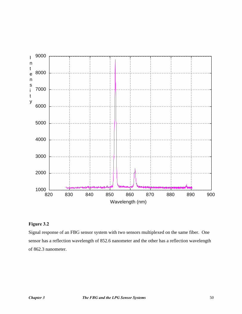
Chapter 3 The FBG and the LPG Sensor Systems 50
Figure 3.2
Signal response of an FBG sensor system with two sensors multiplexed on the same fiber. One
sensor has a reflection wavelength of 852.6 nanometer and the other has a reflection wavelength
of 862.3 nanometer.
820 830 840 850 860 870 880 890 9001000
2000
3000
4000
5000
6000
7000
8000
9000
Wavelength (nm)
Intensity

Chapter 3 The FBG and the LPG Sensor Systems 51
Figure 3.3
Construction of a real-time LPG sensor system. The system having two sensors multiplexed on
the same fiber, but with different transmission loss frequencies.
LPG Sensor
Real Time DigitalSignal Processor
SLED
Analog DataCCD Driver
CCD Array
Diffraction Grating
Static and Non-Volatile MemoriesAnalog to
DigitalConversion
I/O Interface
Control SignalsInterface
High-TemperaturePolymide Coating
TransmissionOptical Fiber
Long PeriodIndex Grating

Chapter 3 The FBG and the LPG Sensor Systems 52
Figure 3.4
Signal response of an LPG sensor. Note that, there are several dips in the transmission spectrum,
each dip corresponds to the coupling of the fundamental guided mode to a different cladding
mode. The intensity in dB is shown relative to the highest transmission loss in the spectrum.
750 800 850 900 9500
2
4
6
8
10
12
Wavelength (nm)
RelativeIntensity(dB)

Chapter 3 The FBG and the LPG Sensor Systems 53
Figure 3.5
Phase matching conditions of mode coupling for (a) Bragg or short period gratings, and (b) long
period gratings [Veng96]. The smaller the differential phase propagation constant ∆β, the longer
the period of gratings Λ.
n1
2πλn
2
2πλ
0
∆ Λβ π= 2 /
− β01
β01
− n2
2πλ− n
1
2πλ
(a)
β
n1
2πλn
2
2πλ
0
∆ Λβ π= 2 /
βcl
1 β01
− n2
2πλ− n
1
2πλ
βcl
2− β
01
(b)
β
Chapter 4 Hardware Development 54
Chapter 4
Hardware Development
All the hardware is designed and developed for the stand alone wavelength modulated optical
fiber sensor system. The system is capable of digitizing and processing all the signals in real
time. All the components and functions of the hardware system are discussed in this chapter.
4.1 S1000 Linear Array CCD Spectrometer
Figure 4.1 shows the picture of an S100 linear array spectrometer of Ocean Optics, Inc.
[OCEA93], which is used for diffracting (with reflection diffraction gratings) the optical
frequency components, of the fiber sensor, at different angles and collecting the corresponding
optical intensities to a linear CCD array. Each element or pixel of the CCD array corresponds to
a particular optical frequency. The S100 has a maximum clock input rate of 2 MHz. The video
output pin of the S1000 sequentially outputs 1100 CCD pixel voltages in analog pulses, at half
the input clock rate, with a range of 0 to 10 volts (added with a user selective offset), at intervals
of 8192 input clock pulses. At the beginning of each integration period, all pixel charges are
transferred at once to CCD registers for sequential read out through the video output pin. After
the transfers, the photodiodes continue to conduct again, and charge is stored proportional to the
light intensity over the integration period. An enable input signal allows to output triggers,
synchronized with the 1100 analog video output pulses, which is at half the rate of the input
clock frequency. The rising edge of the trigger pulses are used as the conversion triggers for the
analog-to-digital conversion of the 1100 analog video output pulses.

Chapter 4 Hardware Development 55
Of the 1100 digitized data points, the first 14 data points are the measure of the analog baseline.
The next 1030 data points are the photodiode readings of which the first 2 and the last 4 are
ineffective diodes, thus making it a 1024 element CCD. The rest of the data points are electrical
zeros.
4.2 Analog-to-Digital Conversion Board
An analog-to-digital conversion board, as shown in the picture of Figure 4.2, is designed and
developed. The analog-to-digital conversion (ADC) board interfaces the CCD spectrometer with
the TMS320C40 board. It digitizes the pulse amplitude signals from the spectrometer using the
conversion trigger pulses, also coming from the spectrometer. The ADC board converts the
analog pulses, each pulse corresponding to a particular CCD element and hence representing the
intensity of a particular optical frequency, into 12-bit parallel digital signals which are interfaced
with the communication ports of the TMS320C40 (henceforth also known as just ‘C40) DSP
chip. The interfacing connections are as shown in Figure 4.3. There are six communication
ports in the ‘C40 chip, and each port can handle 8 parallel data bits. For parallel interfacing of
our 12-bit data we need two communication ports of the ‘C40 chip, Figure 4.3 shows the
interfacing with the Port 3 and 4. Note that after reset, the communication Ports 3, 4, and 5 are
configured as input ports, and the communications Ports 1, 2, and 3 are configured as output
ports [Texa93]. A token forcing circuit is provided, if necessary, in the ADC board, which is
required for an output port to be configured as an input port, or vice versa. For the data
acquisition and processing advantages, the 12-bit data of the ADC board is read as 16-bit data by
the ‘C40 chip, the least significant 4 bits being always zero (i.e. grounded). As the speed of the
‘C40 chip is very high (40 MHz) if compared to the speed of the ADC chip (800 kHz), only a
one way handshaking is implemented for transferring data from the ADC board to the ‘C40
communication ports.

Chapter 4 Hardware Development 56
The Burr-Brown 12-bit analog-to-digital converter, ADS7810, is used for the ADC board. A
brief description of this analog-to-digital converter is provided below.
Analog-to-Digital Converter ADS7810:
The speed of the Ocean Optics’ S1000 spectrometer allows an analog-to-digital converter no
faster than 1 MHz. After extensive vendor search the most suitable ADC chip, for interfacing
with the TMS320C40 communication ports, was decided to be 28-pin Burr-Brown CMOS 12-bit
parallel converter, ADS7810, which is specified at 800 kHz sampling rate, having an industry
standard ±10 V analog input voltage range and a power dissipation under 250 mW [Burr93].
Though a 16-bit ADC were more appropriate for our system, a suitable chip did not exist at the
time of our design with a sampling rate of around 1 MHz.
4.3 TMS320C40 Board
A real-time signal processing board, named the TMS320C40 board, as shown in Figure 4.4, is
designed and developed. The ’C40 board is the mother board of our sensor system. This board
hosts the Texas Instrument’s TMS320C40 (or just ‘C40) floating point digital signal processor,
which is used as the main processor for real time signal processing of the wavelength modulated
optical fiber sensor system. The JTAG (or Boundary Scan) interface of the ‘C40 chip is used to
debug and/or upload/download programs to memory. The ‘C40 board has a universal
asynchronous receiver/transmitter (UART) to connect the system to any computer using the
RS232 communication ports . The RS232 connection is used for the TCP/IP server in any
computer to get access to the sensor system so that the server can send the sensor data in real-
time if requested by any TCP/IP client through the Internet. The RS232 connection can also be
used for any general purpose operations like uploading/downloading programs to/from the sensor

Chapter 4 Hardware Development 57
system, or running a small operating system for the sensor system from any host computer. 128K
of 32-bit words of Non-volatile SRAM and 512K of 32-bit words of fast SRAM is provided on
the ‘C40 board. The non-volatile RAM keeps the system programs and data intact at power off,
and such the system can run by itself at power on. The SRAM can be used for running programs
faster as it has a very small access time. A watchdog timekeeper is provided which keeps track
of time, and can be used to time stamp any data if required, or to put an interrupt to the ‘C40
processor at any predetermined time intervals. Xilinx field-programmable gate arrays are used as
programmable glue logic for timing and interfacing all the components of the ‘C40 board. A
brief description of all the major components of the board are given below.
TMS320C40 DSP Processor:
325-pin grid array TMS320C40 of Texas Instruments, a 32-bit RISC architecture floating point
DSP processor [Tms93], is used as the main processor for our wavelength modulated optical
fiber sensor system. Our processor has a speed rating of 40 MHz, i.e. 50-ns instruction cycle
times. The ‘C40 processor has an instruction set of 145 instructions, the instruction set being
especially well suited to digital signal processing and other numeric-intensive applications. Most
of the instructions take only a single cycle to execute. The floating point instructions are
implemented using 12 (R0-R11) 40-bit wide extended-precision registers. Another 8 (AR0-
AR7) 32-bit wide auxiliary registers are used primarily for address generation. Both the
extended-precision and auxiliary registers can also be used as general purpose 32-bit integer
registers.
The ‘C40 processor has two identical data (32-bit wide) and address (31 bit wide) buses, termed
global and local buses, which support shared memory systems. It has a JTAG interface for IEEE
Boundary Scan and other standard connections. 512 byte of instruction cache and 8 K-byte
single-cycle dual access program or data RAM are provided as on-chip memory in the ‘C40
processor.

Chapter 4 Hardware Development 58
The ‘C40 processor has six bi-directional communications ports and a six-channel DMA
coprocessor for concurrent I/O and CPU operations. Separate internal data, program, and DMA
coprocessor buses support parallel data, program, and I/O operations.
UART PC16550D:
44-pin PC16550D universal asynchronous receiver/transmitter (UART) with FIFOs of National
Semiconductor [Nati95], is used with the ‘C40 board for interfacing the stand alone real-time
signal processing system with any serial communication ports of computers. The PC16550D
performs parallel-to-serial conversion on data characters received from the CPU, and serial-to-
parallel conversion on data characters received from any peripheral device or any MODEM. It
has all the modem control functions, CTS, RTS, DSR, DTR, RI, and DCD. The CPU is capable
of reading the status of the UART (e. g., the error conditions, and the type and conditions of the
transfer), at any time of operation. It can generate and detect even, odd, or no parity, and can add
or delete start, stop, and parity bits. The UART can generate a programmable baud rate ranging
from DC to 1.5M baud, and is capable of handling 5-, 6-, 7-, or 8-bit characters.
SRAM µPD434008 and Nonvolatile SRAM DS1245:
512K-word by 8 bits CMOS fast static RAMs µPD434008LE-20 [Stat95], of NEC Electronics
Inc., are used to design 512K of 32-bit words of SRAM memory. The chips have a small plastic
package of 36 pin. They have a very fast access time of 20-ns maximum.
128K x 8-bit nonvolatile static RAMs DS1245 of Dallas Semiconductor [Dall95a], are used to
design 128K of 32-bit words of nonvolatile memory. It has direct interface with the ‘C40 exactly
like fast SRAM. Each nonvolatile SRAM has a self-contained lithium energy source, which
automatically protects the data in the memory whenever the external power is turned off. It has
10 years minimum data retention capability in the absence of external power, and has unlimited
write cycles with an access time of 70-ns.

Chapter 4 Hardware Development 59
Watchdog Timekeeper DS1286:
Watchdog timekeeper DS1286 of Dallas Semiconductor [Dall95b], is used as watchdog timer, to
keep track of time, or to time-stamp any data, if required. It keeps track of hundredths of
seconds, seconds, minutes, hours, days, date of the month, months, and years, and can generate
separate interrupts at any programmable time intervals and/or when the watchdogged processor
goes out of control. It has an embedded lithium battery source which has a greater than 10 years
of timekeeping in the absence of any external source.
Xilinx FPGA X’C4003A:
Two of the Xilinx field-programmable gate arrays (FPGAs) X’C4003A-4PC84 [Xilin94], are
used to generate, buffer, and interface the control signals of the ‘C40 processor, the PC16550D
UART, and the memory devices. The X’C4003A-4PC84 is a 84-pin PLCC package with
approximate gates count of 3000 and flip-flops count of 360 in a 10 x 10 configurable logic
block (CLB) matrix. These FPGAs are configured by loading a binary file in it, and have
unlimited reprogrammability. The X’C4003A chips provide programmable input pull-up or pull-
down resistors, and programmable output slew rates. The X’C4003A can handle up to 24-mA
sink current per output.
4.4 Programming the Logic for the Xilinx FPGA XC4003A-4PC84
The base package of the Xilinx Foundation Series 6.0.1 software is used to program the logic of
the FPGAs. The programming of the logic can be implemented by using VHDL or by using
schematic capture from the library provided with the Foundation package. The schematic
capture method is used for programming the Xilinx FPGAs as the logic required for our system
is simple. Figure 4.5 and Figure 4.6 shows the schematics of the logic which are implemented in
the Xilinx FPGAs. Once the schematic is drawn and a library for the schematic components is
built, the Foundation software performs full automatic partitioning, placement, and routing of the

Chapter 4 Hardware Development 60
FPGA available resources to implement the logic. The software finally produces a .bit file which
when loaded into the FPGA, the chip gets programmed as the logic of the schematic. The
software has the provision of pre-selecting pins for specific signals
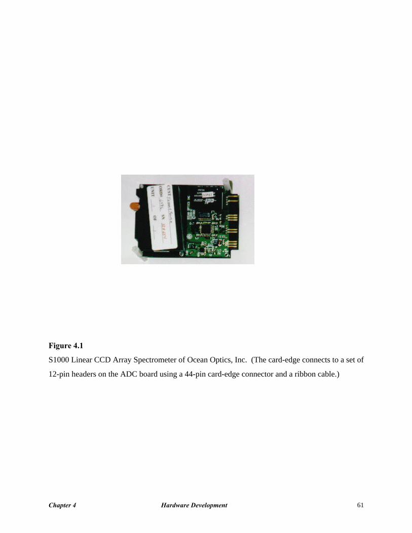
Chapter 4 Hardware Development 61
Figure 4.1
S1000 Linear CCD Array Spectrometer of Ocean Optics, Inc. (The card-edge connects to a set of
12-pin headers on the ADC board using a 44-pin card-edge connector and a ribbon cable.)

Chapter 4 Hardware Development 62
Figure 4.2
The analog-to-digital conversion (ADC) board. (A 32-pin socket, located on the back-side of the
ADC board, directly connects to a set of 32-pin headers, on the back-side of the ‘C40 board.)

Chapter 4 Hardware Development 63
Figure 4.3
Interface connections of the CCD Spectrometer, the ADC chip, and the TMS320C40 chip.
IIOF0 TCLK0
TMS320C40(DSP Processor)
CSTRB5
CSTRB4
C5D(7-0), MS byte
C4D(7-4), rest grounded
VANA R/C
ADS7810(ADC)
CS
BUSY
D(15-4)
S1000 (Linear Array Spectrometer)
VIDEO TRIGGER(↑) Enable_Array CLK
SensingFiber
GND
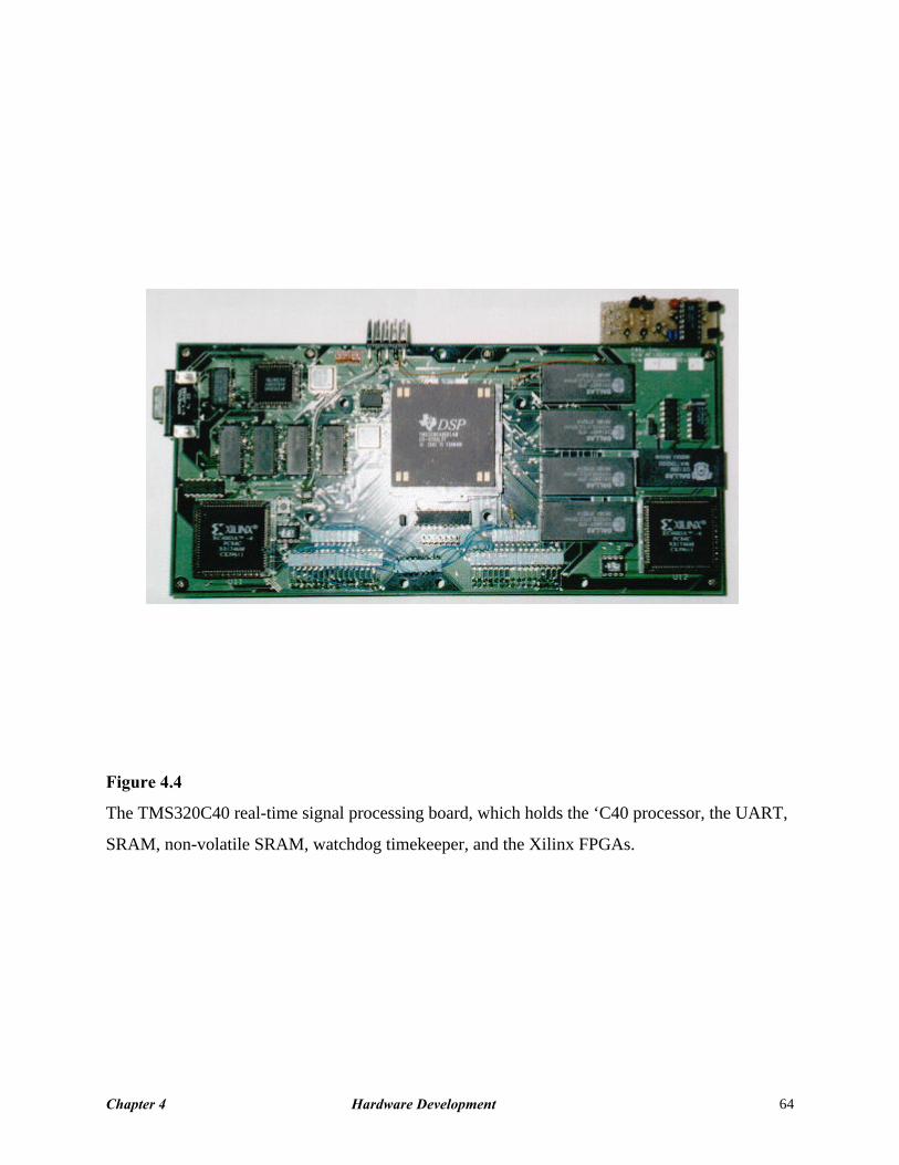
Chapter 4 Hardware Development 64
Figure 4.4
The TMS320C40 real-time signal processing board, which holds the ‘C40 processor, the UART,
SRAM, non-volatile SRAM, watchdog timekeeper, and the Xilinx FPGAs.

Chapter 4 Hardware Development 65
Figure 4.5
Top level schematic of the programmed logic for the Xilinx FPGA XC4003A-4PC84 to generate,
buffer, and interface the control signals of the ‘C40 local buses, the PC16550D UART, and the
SRAM memory devices.

Chapter 4 Hardware Development 66
Figure 4.5 (Cont’d)
Top level schematic of the programmed logic for the Xilinx FPGA XC4003A-4PC84 to generate,
buffer, and interface the control signals of the ‘C40 local buses, the PC16550D UART, and the
SRAM memory devices.
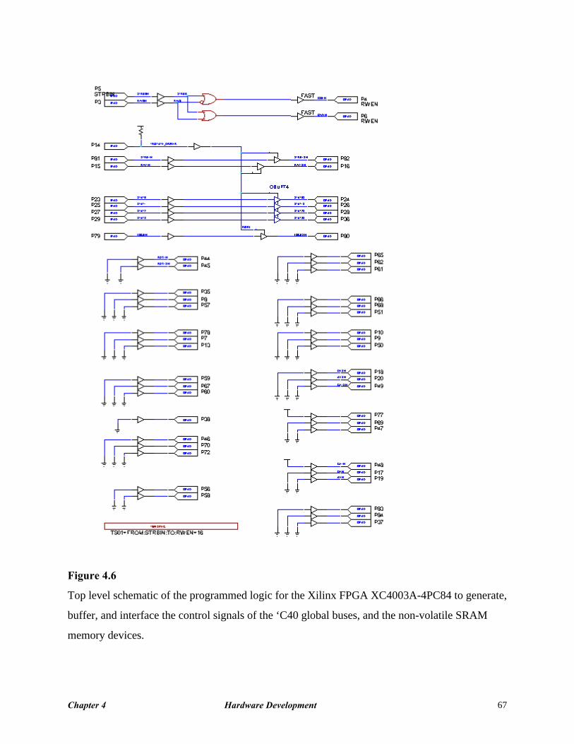
Chapter 4 Hardware Development 67
Figure 4.6
Top level schematic of the programmed logic for the Xilinx FPGA XC4003A-4PC84 to generate,
buffer, and interface the control signals of the ‘C40 global buses, and the non-volatile SRAM
memory devices.

Chapter 5 Firmware and Software Development 68
Chapter 5
Firmware and Software Development
In this chapter we discuss about all the firmware and software developed for the real-time
wavelength modulated optical fiber sensor system. First we discuss about the development of the
digital signal processing (DSP) routines, and then we discuss about the development of the
Internet connectivity software.
5.1 DSP Firmware and Software Development Environment
The Code Composer DSP Development System (version 5.0) for Windows, from GO DSP
Corporation [Code95], and the Texas Instruments ‘C4x DSP tools (the compiler, the assembler,
the linker, the loader, and the ANSI C library functions) of version 4.70 are used for developing
the DSP routines of our wavelength modulated optical fiber sensor system. Also used are some
of the ‘C4x SigTar [Sigt93] and VecTar [Vect93] library functions of TARTAN Inc., presently a
subsidiary of Texas Instruments Inc. The Mountain-510/LT Universal Emulator from White
Mountain DSP Inc. is used for the hardware interface of our ‘C4x system to the PC. The
Mountain-510/LT uses the ‘C4x JTAG connections, and is able to access (upload/download) any
memory locations of the ‘C4x system. The Code Composer must be configured with the
software driver of the Mountain-510/LT to get access to the ‘C4x system.
The Code Composer is a graphical user interface software, and is very handy to write, edit,
compile, assemble, link, and load the program files of any project into the ‘C4x system. It is also
handy to see the contents of a certain memory range of the ‘C4x system in a graph or window, to

Chapter 5 Firmware and Software Development 69
see the values of all the CPU registers in a window, to halt the program flow at any certain
location, to step through any program and display the code in the disassembly window, to
monitor the values of variables from the watch window, and to animate any graph of memory
values while the program is running. It also has features to halt the run time program execution
at any particular memory or code location which make the program debugging very simple.
The Texas Instruments DSP tools allow mixed programming of C and/or assembly. We tried to
develop our programs in C, except where extensive interfacing to registers is required or where
using assembly saves considerable amount of execution time.
5.2 Development of the DSP Firmware and Software
Appendix A lists all the DSP firmware and software routines developed for the stand alone real-
time wavelength modulated optical fiber sensor system. Appendix A.1 and A.2 lists the signal
processing routines for the EFPI sensor and the FBG sensor, respectively. Each sensor system
has its own main() function, which calls all the DSP routines necessary for that particular sensor
system. Some of the routines, e. g., the initialization routines and the data acquisition routine, are
called by all the main() functions.
Presented below are the brief descriptions of all the signal processing routines called by the
main() function of any wavelength modulated optical fiber sensor system.
Chapter 5 Firmware and Software Development 70
5.2.1. The Initialization Routines
The initialization routines are called only once from the main() function. They are not executed
as part of the real-time signal processing routines, rather they initialize the system memories only
once at the system power on.
The function vInitC4x() initializes all the necessary CPU and peripheral bus registers of the ‘C40
processor. The global memory interface control register (GMICR) and the local memory
interface control register (LMICR) set the wait-states and the page sizes of the memory sections
for the global and the local memory strobes, respectively. We require fully software controlled
wait-count of 3 to access the STRB0 UART memory, wait-count of 0 to access the STRB1
SRAM, a wait-count of 1 to access the LSTRB0 non-volatile SRAM, and a wait-count of 7 to
access the LSTRB1 watchdog timekeeper’s memory. The interrupt flag register (IIF) is
initialized to set the pin IIOF2 as a general purpose output signal, which is used as an enable
input to the CCD spectrometer, to start and stop the trigger pulses required for the analog-to-
digital conversions of the CCD video analog pulses. The Timer 0 control register and the Timer
0 period register are set to produce a 1.667 MHz of output clock signal at the TCLK0 pin. After
setting the TCLK0 pin as an output clock, vInitC4x() waits for a while for the clock signal to be
stable, before acquiring any data from the CCD spectrometer, as the TCLK0 signal is used as the
input clock to the CCD spectrometer.
The function vInitUART() initializes all the necessary registers of the UART. It clears all the
flags and removes all the characters, if any, by reading all the registers of the UART.
vInitUART() then sets the baud rate for the UART by initializing the baud register.
The function vCalbPxls() initializes the array of 1024 floating point values with the
corresponding calculated wavelengths of the 1024 elements (starting at element 17) of the Ocean
Optics’ CCD spectrometer. The first 14 CCD pixels, of the 1100-element spectrometer, are
analog baseline and the next 2 pixels are ineffective photodiodes, and thus the first 16 pixel

Chapter 5 Firmware and Software Development 71
elements are not active photodiodes. The coefficients for converting the pixel positions of the
array into wavelengths are unique for any particular CCD spectrometer. The coefficients are
provided by the Ocean Optics Inc., along with the CCD spectrometer.
5.2.2. The Data Acquisition Routine
The function nAcqData(int *iaData, int *iaDMA3_DEST, int *iaDMA4_DEST), acquires a set
of 1100 integer data from the CCD spectrometer, using DMA interrupts, and saves them in an
array pointed by iaData. As nAcqData() is implemented in assembly language, there are lots of
‘C40 register accesses involved in it, it is important to remember the order of argument transfers
into the stack if we want to retrieve them from the assembly environment. In Texas Instruments’
‘C40 compiler the rightmost argument is PUSHed first into the stack and the leftmost argument
is PUSHed last. As the ‘C40 stack is of pre-incrementing, the leftmost argument has a higher
address location in the stack than the rightmost argument.
As shown in Figure 4.1, each 12-bit digital datum is received in parallel by the ‘C40
communication ports 3 and 4. Communication port 4 receives the MS 8-bit of the datum, and the
communication port 3 receives the LS 4-bit of the datum as the MS nibble, the LS nibble being
permanently grounded. Even though the ‘C40 communication ports receive data in bytes, they
are saved as 32-bit words, the first byte received being considered as the LS byte of the word.
Thus the 1100 data set received by the communication ports 3 and 4, are first saved as two sets of
275 words, each word of any of these two sets having 4 bytes, each byte coming from a different
datum. Note that at reset the ‘C40 communication ports 3, 4, and 5 are configured as input ports,
and ports 0, 1, and 2 are configured as output ports.
The function nAcqData() first resets the DMA3 and DMA4 input queues, and then initializes all
the DMA3 and DMA4 registers to receive 275 words each, at locations pointed by
iaDMA3_DEST and iaDMA4_DEST, from the communication ports 3 and 4 respectively. DMA

Chapter 5 Firmware and Software Development 72
is set to have a higher priority than the CPU. nAcqData() then enables the DMA interrupt and
also enables the CCD spectrometer using the IIOF2 signal and waits in a loop and checks the
DMA transfers until the 1100 data set is completely acquired or it may time out by counting
down a predetermined number. It then disables both the CCD enable and the DMA interrupt
enable, and calls the UNMINGLE subroutine, after proper register initializations, to unmingle the
byte mingled data from two separate 275-word locations into a 1100 sign-extended 16-bit integer
values, and to save that at location pointed by iaData. If nAcqData() times out in the wait loop, it
returns with an error code of -1, otherwise if the data acquisition is successful it returns with a
value of 0.
5.2.3. The UART Service Routine
The function nServUART(), if called, checks if there is any request for sending the set of acquired
1100 integer CCD data through the UART. If it finds the request 'S', it sends the 1100 data with
the preamble (123456789) and the post-signature (987654321) and returns with a value of 0.
Otherwise it returns with a value of -1.
The UART sends (or receives) data as characters. A 32-bit word integer is sent as 4 characters of
1 byte each. The routine is implemented such that the MS byte of the integer is sent first, and the
LS byte of the integer is sent last. All the transfers are done through a hardware handshake, and
can cause considerable delay in real-time implementations.
5.2.4. The EFPI Signal Processing Routines
The function vFltrBw3() performs a high-pass filtering to the data with third order Butterworth
coefficients having a normalized cutoff frequency of 0.02. The filtering primarily gets rid off the
DC values present in the data.

Chapter 5 Firmware and Software Development 73
The function fftr() is a Tartan SigTar optimized signal processing library function [Sigt93]. It
performs a 1024 point in-place fast Fourier transform (FFT) on the filtered data.
The function cvabs() is a Tartan VecTar vector math library function [Vect93]. It basically finds
the magnitude of the complex FFT data returned by fftr().
The function maxv() is also a Tartan VecTar vector math library function. It finds the maximum
value of the magnitude of the complex FFT data, along with its index in the array.
The function vFindFloatPix() finds the index of the maximum value of the FFT magnitudes of
the data more precise than just an integer. It makes a Gaussian approximation with three FFT
magnitude values, the maximum value and the two values just either side of the maximum value,
and tries to find the floating point index of the real peak, as if the points were continuous.
The function vFindTruGap() finds the gap of the EFPI sensor using the discrete lambda
transform (DLT). It uses the ‘golden search rule’ [Press88], and the estimated gap to reduce the
number of DLT transformation, as it is very computationally intensive if compared to other
functions.
The function vDGT() performs the discrete gap transformation (DGT) on the data for the given
EFPI gap, and finds the DGT magnitude for it.
5.2.5. The FBG Signal Processing Routines
Appendix A.2 include the FBG signal processing routine, vFindPks(), used for the real-time FBG
optical fiber sensor system. The function vFindPks() calculates the wavelength locations of all
the Bragg peaks from the 1100 floating point data values using a centroid method, as discussed in

Chapter 5 Firmware and Software Development 74
section 3.5. The number, the ranges, and the widths of the Bragg peaks must be provided with
the function call.
5.2.6. The Memory Allocation File
Appendix A.4 lists the memory allocation file (also known as .CMD file) required for the Texas
Instruments’ DSP tools to load programs on the ‘C40 system. It first declares and assigns a name
to all the valid addressable memory ranges, and then instructs the loader where to load different
program sections in those memory ranges.
5.3 The TCP/IP Client/Server Software Development Environment
All the TCP/IP client/server graphical user interface software were developed with the
LabWindows-CVI (version 4.0) software environment of National Instruments Inc. It has
extensive library support in the areas of user interfaces, RS232 communications, and the TCP/IP
client/server communications. We used these library functions in C to implement the
client/server software and hence to interface the real-time wavelength modulated optical fiber
sensor system to the Internet
5.4 Development of the TCP/IP Client/Server Software
Appendix B lists all the TCP/IP client/server software developed to interface our real-time
wavelength modulated optical fiber sensor system to the Internet, as depicted in Figure 5.1. One
is able to acquire the data through the Internet from the ‘C40 system from anywhere in the world,
by using this client/server software.
Chapter 5 Firmware and Software Development 75
Given below are brief descriptions of the client/server routines developed to acquire data through
the Internet from the ‘C40 system in real-time.
5.4.1 TCP/IP Client Programs
Appendix B.1 shows the graphical user interface panel for the TCP/IP server, and B.2 lists the
programs to run the client. When the client program is executed it prompts the user either for the
name or the Internet Protocol (IP) address of the machine running the server. The program then
prompts the user for the TCP/IP port number set for the server. It then loads the graphical user
interface panel along with its menu and controls, and initiates a connection to the server. If the
connection initiation is failed it lets user know about that and ends the graphical user interface
and the program. If the connection initiation is successful it makes the color of a control button
green to indicate that it is connected to the server. Using the pull-down menu of the client
graphical user interface panel, one can send a request to the server to send the real-time 1100
integer data set of the CCD spectrometer from the ‘C40 system. Upon receiving the data from
the server, the client program displays it on the graph panel. One can also initiate a continuous
request, in which case the graph panel is updated continuously with the real-time data.
The pull-down menu of the client panel also supports that any data set be saved in a file, or that
any data set be read from a file and be displayed on the graph.
5.4.2 TCP/IP Server Programs
Appendix B.3 shows the graphical user interface panel for the TCP/IP server, and B.4 lists the
programs to run the server. When the server is started it prompts the user to input the serial
(RS232) communication port number to communicate to the ‘C40 sensor system, and initializes
Chapter 5 Firmware and Software Development 76
that port with the baud rate and other protocols supported by the UART of the ‘C40 system. The
program then prompts the user to input a TCP/IP port number for the server. This port number
must be used by any client to make any connection to the server. The graphical user interface
panel is loaded then, with its menu and controls, and runs the TCP/IP server, and waits for any
TCP/IP client to make connection to it and to request data. If requested, it downloads the set of
1100 integer CCD data by checking the preamble and the post-signature of the data set, from the
‘C40 system through the RS232 comport and transmits them to the client through the Internet.
While downloading the 32-bit integer data as 8-bit characters, it must be remembered that the
UART of the ‘C40 system sends the MS-byte of each datum first and the LS-byte last. If any
client is currently connected to the server, the server panel indicates that with a control button by
changing its color to green.

Chapter 5 Firmware and Software Development 77
Figure 5.1
Block level diagram of the networking connections of the real-time wavelength modulated sensor
system with the Internet.
Computer
ComputerPrinter
Gateway/Server
Computer
The ‘C40Sensor System
LANThe Internet