read-only uhf rfid ic - em microelectronic · read-only uhf rfid ic description the chip is used in...
TRANSCRIPT
EM4123
Copyright 2014, EM Microelectronic-Marin SA 4123-DS.doc, Version 6.0, 17-Nov-14
1 www.emmicroelectronic.com
Read-only UHF RFID IC
Description The chip is used in passive UHF read-only transponder applications. It is powered up by an RF beam transmitted by the reader, which is received and rectified to generate a supply voltage for the chip. A pre-programmed code is transmitted to the reader by varying the amount of energy that is reflected back to the reader. It implements a robust and fast anti-collision protocol. The chip is frequency independent and can be used for RF coupled applications where reading ranges in excess of 10 m and reading rates of 120 tags per second at 256 kbit/s can be attained. The chip is backscattering data using load modulation. Therefore the reader should be able to detect ASK and PSK modulated carrier.
Typical Applications The chip is ideal for applications where long range, high-speed item identification is required: Supply chain management Tracking and tracing Access control Asset control Licensing Auto-tolling Animal tagging Sports event timing
Features Factory programmed 64 bit ID number High data rate: Up to 256 kbit/s Frequency independent: Typically used at 869
MHz, 902 - 960 MHz (versions 001 to 099) On-chip oscillator On-chip rectifier Low voltage operation - down to 1.0 V at ambient
temperature Tag Talk Only protocol (TTO) Low power consumption Low cost
-40° to +85° C operating temperature range
Benefits Anti-collision suited to flux monitoring Very low consumption High backscatter amplitude Designed for ease of antenna attachment
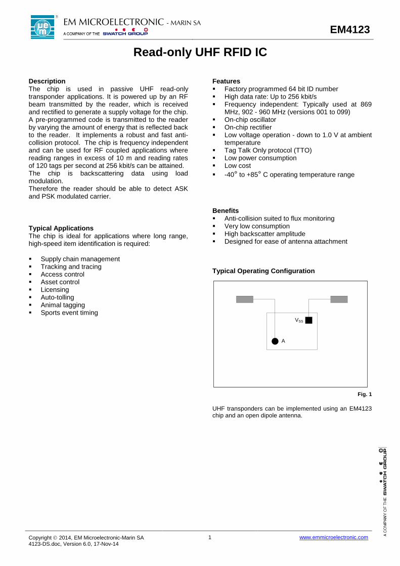
Typical Operating Configuration
VSS
A
Fig. 1
UHF transponders can be implemented using an EM4123 chip and an open dipole antenna.
EM MICROELECTRONIC - MARIN SA
EM4123
Copyright 2014, EM Microelectronic-Marin SA 4123-DS.doc, Version 6.0, 17-Nov-14
2 www.emmicroelectronic.com
Absolute Maximum Ratings Parameter Symbol Conditions
Maximum RMS current supplied into A
IA
10 mA
Storage temperature TSTORE -55 to +125oC
Electrostatic discharge maximum to MIL-STD-883C method 3015
Version 001 to 099
VESD 2 KV
Stresses above these listed maximum ratings may cause permanent damage to the device. Exposure beyond specified operating conditions may affect device reliability or cause malfunction.
Handling Procedures This device has built-in protection against high static voltages or electric fields; however, due to the unique properties of this device, anti-static precautions should be taken as for any other CMOS component. Unless otherwise specified, proper operation can only occur when all the terminal voltages are kept within the supply voltage range.
Operating Conditions Parameter Symbol Min Typ Max Units
Operating temperature
TA -40 +85 oC
RMS current supplied into A
10 mA
Electrical Characteristics VA - VSS = 2.0 V, TA = 25°C, unless otherwise specified.
Parameter Symbol Test conditions Min Typ Max Units
Oscillator frequency FOSC -40°C to +85°C 400 512 600 kHz
Wake-up voltage VWU VA – VSS rising 1.0 1.4 1.8 V
Static current consumption ISTAT VA – VSS = 1 V 1 5 A
Input series impedance
Zin
PDUT = -12 dBm; Die form fa = 868 MHz; fa = 915 MHz;
20-j530 20-j500
40-j590 40-j560
50-j650 50-j620
PDUT = -12 dBm; SC70 3L fa = 868 MHz; fa = 915 MHz; fa = 953 MHz;
9.6-j214 10.1-j204 9.4-j195
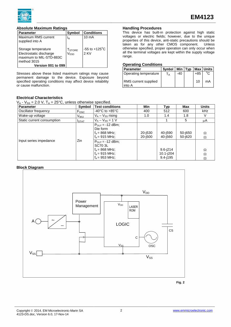
Block Diagram
Fig. 2
VDD
VSS
C
OSC
CS
VSS
VDD
LOGIC A
LASER ROM
VSS
~ _
Power Management
EM4123
Copyright 2014, EM Microelectronic-Marin SA 4123-DS.doc, Version 6.0, 17-Nov-14
3 www.emmicroelectronic.com
Functional Description
Shunt regulator The shunt regulator has two functions. It limits the voltage across the logic and protects the Schottky rectifier diodes.
Oscillator The on-chip RC oscillator has a center frequency of 512 kHz. It supplies a clock to the logic and defines the data rate.
Wake-up voltage The reset signal keeps the logic in reset when the supply voltage is lower than the threshold voltage. This prevents incorrect operation and spurious transmissions when the supply voltage is too low for the oscillator and logic to work properly. It also ensures that transistor Q2 is off and transistor Q1 is on during power-up to ensure that the chip starts up.
Modulation transistor The N channel transistor Q2 is used to modulate the transponder antenna. When it is turned on it loads the antenna, thereby changing the load seen by the reader antenna, and effectively changing the RCS of the tag and the amount of energy that is reflected to the reader. Q2 is active for Data Out = "1".
Antenna adaptation The antenna attached to the pads A and VSS should have an impedance at the operating frequency equal to the conjugate math of the chip's impedance. This adaptation is required for best energy transfer and maximum of reflection coefficient.
Charge preservation transistor The P channel transistor Q1 is turned off whenever the modulation transistor Q2 is turned on to prevent Q2 from discharging the power storage capacitor (CS). This is done in a break-before-make manner, i.e. Q1 is first turned off before Q2 is turned on, and Q2 is turned off before Q1 is turned on.
LOGIC block After the power-on reset has disappeared, the chip boots by reading a seed value into the random number generator. The least significant 16 bits of the ID (the CRC) is used as a seed. The chip then enters its normal operating mode, which consists of clocking a 16 bit timer counter with the bit rate clock until it compares with the number in the random number generator. At this point a code is transmitted. The random number generator is clocked to generate a new pseudo random number, and the 16 bit counter is reset to start a new delay. The width of the comparison between the 16 bit random number and the 16 bit delay count determines the maximum possible delay between transmissions (reading rate). Any one of four maximum delay settings can be pre-programmed.
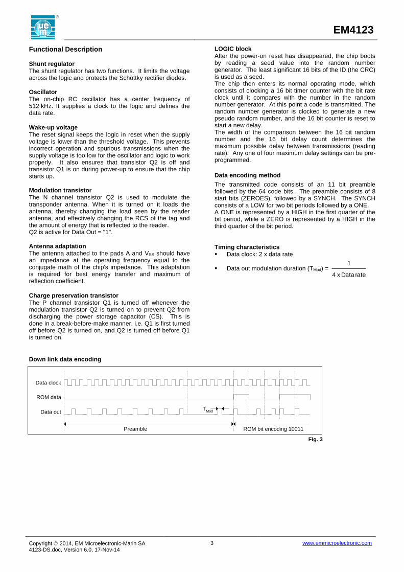
Data encoding method
The transmitted code consists of an 11 bit preamble followed by the 64 code bits. The preamble consists of 8 start bits (ZEROES), followed by a SYNCH. The SYNCH consists of a LOW for two bit periods followed by a ONE. A ONE is represented by a HIGH in the first quarter of the bit period, while a ZERO is represented by a HIGH in the third quarter of the bit period.
Timing characteristics Data clock: 2 x data rate
Data out modulation duration (TMod) = rate Data x 4
1
Down link data encoding
Preamble
TMod
ROM bit encoding 10011
Data clock
ROM data
Data out
Fig. 3
EM4123
Copyright 2014, EM Microelectronic-Marin SA 4123-DS.doc, Version 6.0, 17-Nov-14
4 www.emmicroelectronic.com
ROM programming The EM4123 contains two laser fuse ROM blocks that are pre-programmed by the foundry. The ROM blocks are split in two parts: the Code ID ROM and the Control ROM.
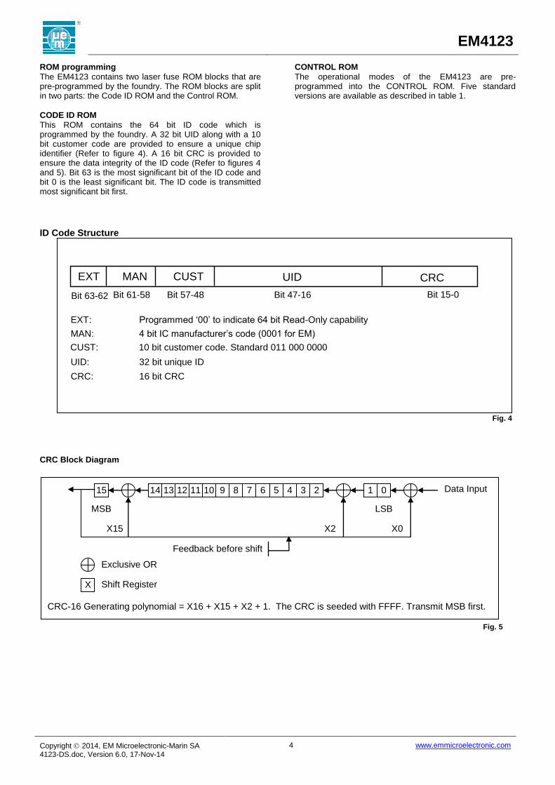
CODE ID ROM This ROM contains the 64 bit ID code which is programmed by the foundry. A 32 bit UID along with a 10 bit customer code are provided to ensure a unique chip identifier (Refer to figure 4). A 16 bit CRC is provided to ensure the data integrity of the ID code (Refer to figures 4 and 5). Bit 63 is the most significant bit of the ID code and bit 0 is the least significant bit. The ID code is transmitted most significant bit first.
CONTROL ROM The operational modes of the EM4123 are pre-programmed into the CONTROL ROM. Five standard versions are available as described in table 1.
ID Code Structure
Fig. 4
CRC Block Diagram
CRC-16 Generating polynomial = X16 + X15 + X2 + 1. The CRC is seeded with FFFF. Transmit MSB first.
Fig. 5
Bit 63-62 Bit 61-58 Bit 15-0
CRC
UID
MAN
EXT
EXT: Programmed ‘00’ to indicate 64 bit Read-Only capability
capability
MAN: 4 bit IC manufacturer’s code (0001 for EM)
EM)
UID:
32 bit unique ID
Bit 57-48 Bit 47-16
CUST
CRC: 16 bit CRC
CUST: 10 bit customer code. Standard 011 000 0000
15 14 13 12 11 10 9 8 7 6 5 4 3 2 1 0
X
X15
MSB
X2
LSB
X0
Exclusive OR
Shift Register
Data Input
Feedback before shift
EM4123
Copyright 2014, EM Microelectronic-Marin SA 4123-DS.doc, Version 6.0, 17-Nov-14
5 www.emmicroelectronic.com
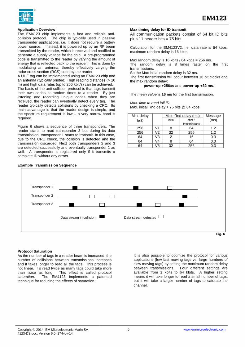
Application Overview The EM4123 chip implements a fast and reliable anti-collision protocol. The chip is typically used in passive transponder applications, i.e. it does not require a battery power source. Instead, it is powered up by an RF beam transmitted by the reader, which is received and rectified to generate a supply voltage for the chip. A pre-programmed code is transmitted to the reader by varying the amount of energy that is reflected back to the reader. This is done by modulating an antenna, thereby effectively varying the radar cross section (RCS) seen by the reader. A UHF tag can be implemented using an EM4123 chip and an antenna (typically printed). High reading distances (> 10 m) and high data rates (up to 256 kbit/s) can be achieved. The basis of the anti-collision protocol is that tags transmit their own codes at random times to a reader. By just listening and recording unique codes when they are received, the reader can eventually detect every tag. The reader typically detects collisions by checking a CRC. Its main advantage is that the reader design is simple, and the spectrum requirement is low – a very narrow band is required. Figure 6 shows a sequence of three transponders. The reader starts to read transponder 3 but during its data transmission, transponder 1 starts to transmit. In this case, due to the CRC check, the collision is detected and the transmission discarded. Next both transponders 2 and 3 are detected successfully and eventually transponder 1 as well. A transponder is registered only if it transmits a complete ID without any errors.
Max timing delay for ID transmit
All communication packets consist of 64 bit ID bits plus 11 header bits = 75 bits. Calculation for the EM4123V2, i.e. data rate is 64 kbps, maximum random delay is 16 kbits. Max random delay is 16 kbits / 64 kbps = 256 ms. The random delay is 8 times faster on the first transmissions. So the Max initial random delay is 32 ms. The first transmission will occur between 16 bit clocks and the max random delay:
power-up +256s and power-up +32 ms.
The mean value is 16 ms for the first transmission. Max. time to read full ID: Max. initial Rnd delay + 75 bits @ 64 kbps
Min. delay
(s)
Max. Rnd delay (ms) Message (ms) Initial after 6
transmissions
256 V1 8 64 1.2
256 V2 32 256 1.2
64 V3 2 16 0.3
64 V4 8 64 0.3
64 V5 32 256 0.3
Example Transmission Sequence
Fig. 6
Protocol Saturation As the number of tags in a reader beam is increased, the number of collisions between transmissions increases and it takes longer to read all the tags. This process is not linear. To read twice as many tags could take more than twice as long. This effect is called protocol saturation. The EM4123 implements a patented technique for reducing the effects of saturation.
It is also possible to optimize the protocol for various applications (few fast moving tags vs. large numbers of slow moving tags) by setting the maximum random delay between transmissions. Four different settings are available from 1 kbits to 64 kbits. A higher setting means it will take longer to read a small number of tags, but it will take a larger number of tags to saturate the
channel.
Transponder 2
Transponder 1
Data stream in collision Data stream detected
Transponder 3
EM4123
Copyright 2014, EM Microelectronic-Marin SA 4123-DS.doc, Version 6.0, 17-Nov-14
6 www.emmicroelectronic.com
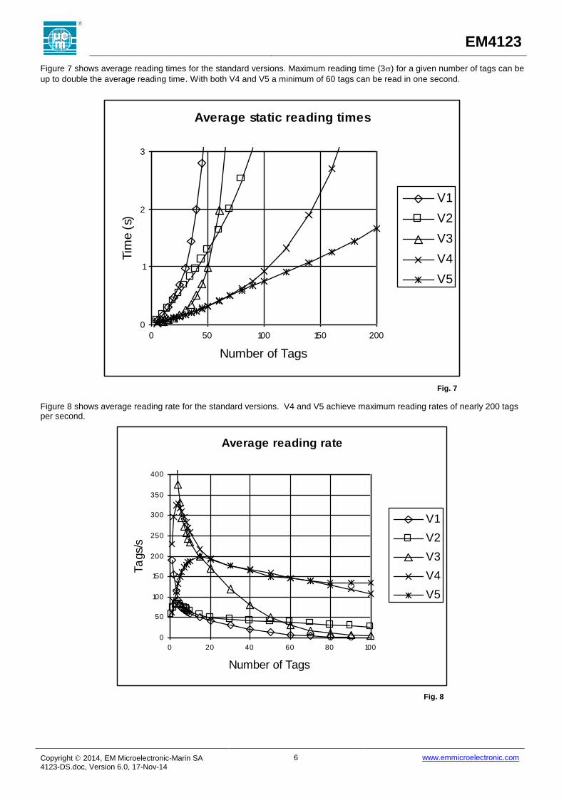
Figure 7 shows average reading times for the standard versions. Maximum reading time (3) for a given number of tags can be
up to double the average reading time. With both V4 and V5 a minimum of 60 tags can be read in one second.
Average static reading times
0
1
2
3
0 50 100 150 200
Number of Tags
Tim
e (
s)
V1
V2
V3
V4
V5
Fig. 7
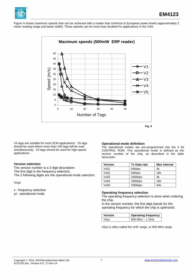
Figure 8 shows average reading rate for the standard versions. V4 and V5 achieve maximum reading rates of nearly 200 tags per second.
Average reading rate
0
50
100
150
200
250
300
350
400
0 20 40 60 80 100
Number of Tags
Ta
gs/
s
V1
V2
V3
V4
V5
Fig. 8
EM4123
Copyright 2014, EM Microelectronic-Marin SA 4123-DS.doc, Version 6.0, 17-Nov-14
7 www.emmicroelectronic.com
Figure 9 shows maximum speeds that can be achieved with a reader that conforms to European power levels (approximately 2 meter reading range and beam width). These speeds can be more than doubled for applications in the USA.
Maximum speeds (500mW ERP reader)
0
5
10
15
20
25
30
35
40
45
50
0 10 20 30 40 50
Number of Tags
Speed (
m/s
) V1
V2
V3
V4
V5
Fig. 9
V4 tags are suitable for most SCM applications. V5 tags should be used where more than 100 tags will be read simultaneously. V3 tags should be used for high-speed applications.
Version selection The version number is a 3 digit description. The first digit is the frequency selection; The 2 following digits are the operational mode selection. Vxyz x : frequency selection yz : operational mode
Operational mode definition The operational modes are pre-programmed into the 5 bit CONTROL ROM. This operational mode is defined as the version number of the chip, as described in the table hereunder.
Version Tx Data rate Max interval
Vx01 64kbps 4k
Vx02 64kbps 16k
Vx03 256kbps 4k
Vx04 256kbps 16k
Vx05 256kbps 64k
Operating frequency selection The operating frequency selection is done when ordering the chip. In the version number, the first digit stands for the operating frequency for which the chip is optimized:
Version Operating frequency
V0yz 800 MHz – 1 GHz
V0yz is often called the UHF range, or 900 MHz range
EM4123
Copyright 2014, EM Microelectronic-Marin SA 4123-DS.doc, Version 6.0, 17-Nov-14
8 www.emmicroelectronic.com
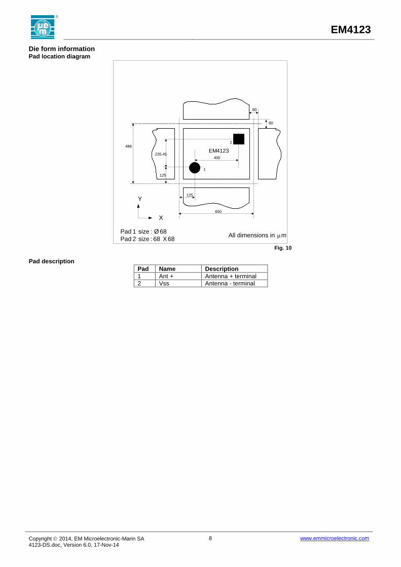
Die form information Pad location diagram
EM4123
All dimensions in m
Y
X650
486
125
Pad 1 size : Ø 68
Pad 2 size : 68 X 68
125
2
400
80
80
1
235.45
Fig. 10
Pad description
Pad Name Description
1 Ant + Antenna + terminal
2 Vss Antenna - terminal
EM4123
Copyright 2014, EM Microelectronic-Marin SA 4123-DS.doc, Version 6.0, 17-Nov-14
9 www.emmicroelectronic.com
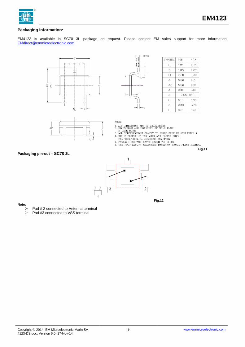
Packaging information: EM4123 is available in SC70 3L package on request. Please contact EM sales support for more information. [email protected]
Fig.11
Packaging pin-out – SC70 3L
Fig.12
Note:
Pad # 2 connected to Antenna terminal Pad #3 connected to VSS terminal
EM4123
Copyright 2014, EM Microelectronic-Marin SA 4123-DS.doc, Version 6.0, 17-Nov-14
10 www.emmicroelectronic.com
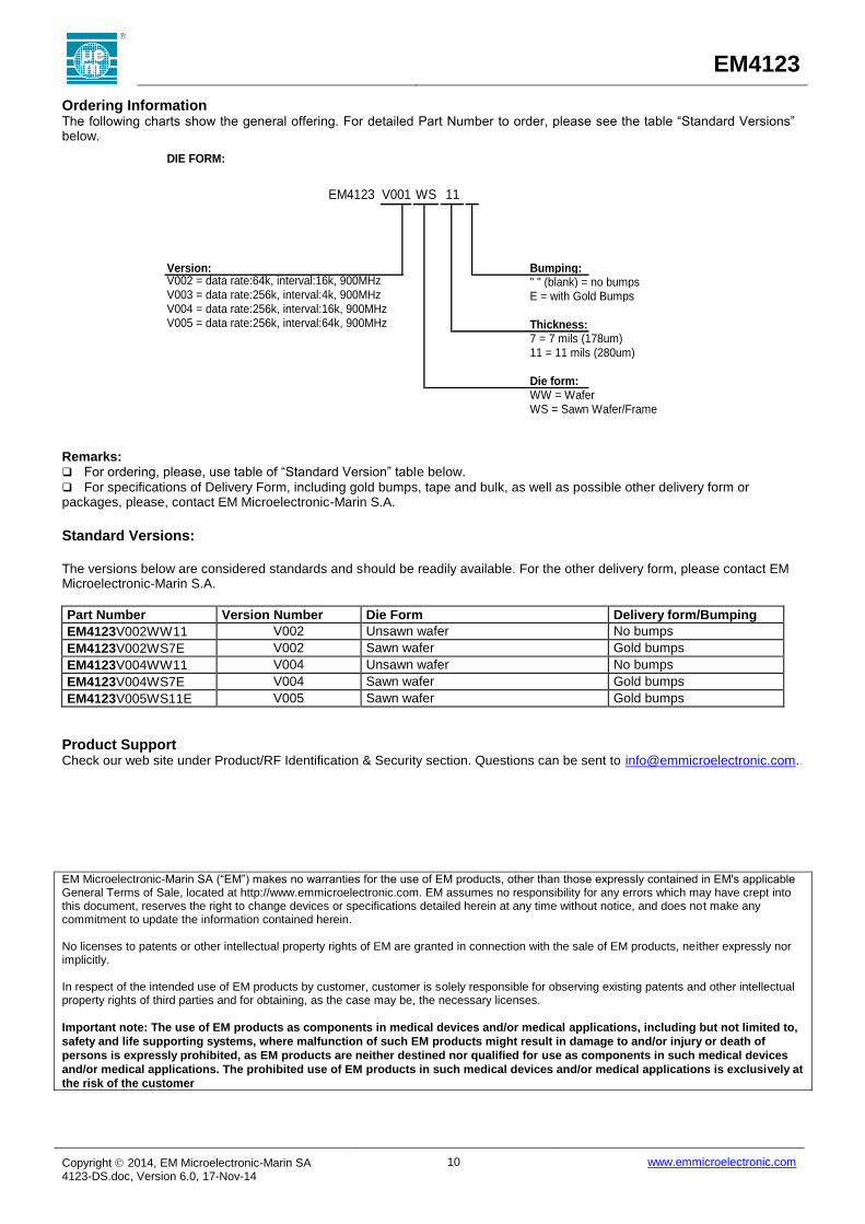
Ordering Information The following charts show the general offering. For detailed Part Number to order, please see the table “Standard Versions” below.
Remarks: For ordering, please, use table of “Standard Version” table below.
For specifications of Delivery Form, including gold bumps, tape and bulk, as well as possible other delivery form or packages, please, contact EM Microelectronic-Marin S.A.
Standard Versions:
The versions below are considered standards and should be readily available. For the other delivery form, please contact EM Microelectronic-Marin S.A.
Part Number Version Number Die Form Delivery form/Bumping
EM4123V002WW11 V002 Unsawn wafer No bumps
EM4123V002WS7E V002 Sawn wafer Gold bumps
EM4123V004WW11 V004 Unsawn wafer No bumps
EM4123V004WS7E V004 Sawn wafer Gold bumps
EM4123V005WS11E V005 Sawn wafer Gold bumps
Product Support Check our web site under Product/RF Identification & Security section. Questions can be sent to [email protected]. EM Microelectronic-Marin SA (“EM”) makes no warranties for the use of EM products, other than those expressly contained in EM's applicable General Terms of Sale, located at http://www.emmicroelectronic.com. EM assumes no responsibility for any errors which may have crept into this document, reserves the right to change devices or specifications detailed herein at any time without notice, and does not make any commitment to update the information contained herein. No licenses to patents or other intellectual property rights of EM are granted in connection with the sale of EM products, neither expressly nor implicitly. In respect of the intended use of EM products by customer, customer is solely responsible for observing existing patents and other intellectual property rights of third parties and for obtaining, as the case may be, the necessary licenses.
Important note: The use of EM products as components in medical devices and/or medical applications, including but not limited to,
safety and life supporting systems, where malfunction of such EM products might result in damage to and/or injury or death of
persons is expressly prohibited, as EM products are neither destined nor qualified for use as components in such medical devices
and/or medical applications. The prohibited use of EM products in such medical devices and/or medical applications is exclusively at
the risk of the customer
DIE FORM:
Version: Bumping:V002 = data rate:64k, interval:16k, 900MHz " " (blank) = no bumpsV003 = data rate:256k, interval:4k, 900MHz E = with Gold BumpsV004 = data rate:256k, interval:16k, 900MHzV005 = data rate:256k, interval:64k, 900MHz Thickness:
7 = 7 mils (178um)11 = 11 mils (280um)
Die form:WW = WaferWS = Sawn Wafer/Frame
EM4123 V001 WS 11