reactive power compensation using an energy management … · reactive power compensation using an...
TRANSCRIPT

Calhoun: The NPS Institutional Archive
Theses and Dissertations Thesis Collection
2014-09
Reactive power compensation using an energy
management system
Prato, Michael V.
Monterey, California: Naval Postgraduate School
http://hdl.handle.net/10945/43982

NAVAL POSTGRADUATE
SCHOOL
MONTEREY, CALIFORNIA
THESIS
Approved for public release; distribution is unlimited
REACTIVE POWER COMPENSATION USING AN ENERGY MANAGEMENT SYSTEM
by
Michael V. Prato
September 2014
Thesis Advisor: Alexander L. Julian Co-Advisor: Giovanna Oriti

THIS PAGE INTENTIONALLY LEFT BLANK

i
REPORT DOCUMENTATION PAGE Form Approved OMB No. 0704–0188 Public reporting burden for this collection of information is estimated to average 1 hour per response, including the time for reviewing instruction, searching existing data sources, gathering and maintaining the data needed, and completing and reviewing the collection of information. Send comments regarding this burden estimate or any other aspect of this collection of information, including suggestions for reducing this burden, to Washington headquarters Services, Directorate for Information Operations and Reports, 1215 Jefferson Davis Highway, Suite 1204, Arlington, VA 22202–4302, and to the Office of Management and Budget, Paperwork Reduction Project (0704–0188) Washington DC 20503.
1. AGENCY USE ONLY (Leave blank)
2. REPORT DATE September 2014
3. REPORT TYPE AND DATES COVERED Master’s Thesis
4. TITLE AND SUBTITLE REACTIVE POWER COMPENSATION USING AN ENERGY MANAGEMENT SYSTEM
5. FUNDING NUMBERS
6. AUTHOR(S) Michael V. Prato
7. PERFORMING ORGANIZATION NAME(S) AND ADDRESS(ES) Naval Postgraduate School Monterey, CA 93943–5000
8. PERFORMING ORGANIZATION REPORT NUMBER
9. SPONSORING /MONITORING AGENCY NAME(S) AND ADDRESS(ES) N/A
10. SPONSORING/MONITORING AGENCY REPORT NUMBER
11. SUPPLEMENTARY NOTES The views expressed in this thesis are those of the author and do not reflect the official policy or position of the Department of Defense or the U.S. Government. IRB Protocol number ____N/A____.
12a. DISTRIBUTION / AVAILABILITY STATEMENT Approved for public release; distribution is unlimited
12b. DISTRIBUTION CODE
13. ABSTRACT (maximum 200 words) A significant contributor to higher energy costs and reduced energy efficiency is the reactive power demand on the grid. Inductive power demand reduces power factor, increases energy losses during transmission, limits real power supplied to the consumer, and results in higher costs to the consumer. Compensating for a reactive power demand on the grid by providing reactive power support to the power distribution system creates energy efficiency gains and improves cost savings.
One method of compensating for reactive power is by incorporating an energy management system (EMS) into the power distribution system. An EMS can monitor reactive power requirements on the grid and provide reactive power support at the point of common coupling (PCC) in the power distribution system in order to increase energy efficiency.
The use of an EMS as a current source to achieve a unity power factor at the grid is demonstrated in this thesis. The power factor angle was determined using a zero-crossing detection algorithm. The appropriate amount of compensating reactive current was then injected into the system at the PCC and controlled using closed-loop current control. The process was simulated using Simulink and then validated in the laboratory using the actual EMS hardware.
14. SUBJECT TERMS Reactive power, reactive power compensation, reactive power control, reactive power demand, power factor, power factor improvement, power factor correction, energy management system, EMS, power loss, reactive power loss, zero-crossing detection, closed-loop current control, energy efficiency, energy cost savings
15. NUMBER OF PAGES
77
16. PRICE CODE
17. SECURITY CLASSIFICATION OF REPORT
Unclassified
18. SECURITY CLASSIFICATION OF THIS PAGE
Unclassified
19. SECURITY CLASSIFICATION OF ABSTRACT
Unclassified
20. LIMITATION OF ABSTRACT
UU NSN 7540–01–280–5500 Standard Form 298 (Rev. 2–89) Prescribed by ANSI Std. 239–18

ii
THIS PAGE INTENTIONALLY LEFT BLANK

iii
Approved for public release; distribution is unlimited
REACTIVE POWER COMPENSATION USING AN ENERGY MANAGEMENT SYSTEM
Michael V. Prato Major, United States Marine Corps B.S., University of Illinois, 2001
Submitted in partial fulfillment of the requirements for the degree of
MASTER OF SCIENCE IN ELECTRICAL ENGINEERING
from the
NAVAL POSTGRADUATE SCHOOL September 2014
Author: Michael V. Prato
Approved by: Alexander L. Julian Thesis Advisor
Giovanna Oriti Co-Advisor
R. Clark Robertson Chair, Department of Electrical and Computer Engineering

iv
THIS PAGE INTENTIONALLY LEFT BLANK

v
ABSTRACT
A significant contributor to higher energy costs and reduced energy efficiency is the
reactive power demand on the grid. Inductive power demand reduces power factor,
increases energy losses during transmission, limits real power supplied to the consumer,
and results in higher costs to the consumer. Compensating for a reactive power demand
on the grid by providing reactive power support to the power distribution system creates
energy efficiency gains and improves cost savings.
One method of compensating for reactive power is by incorporating an energy
management system (EMS) into the power distribution system. An EMS can monitor
reactive power requirements on the grid and provide reactive power support at the point
of common coupling (PCC) in the power distribution system in order to increase energy
efficiency.
The use of an EMS as a current source to achieve a unity power factor at the
grid is demonstrated in this thesis. The power factor angle was determined using a zero-
crossing detection algorithm. The appropriate amount of compensating reactive current
was then injected into the system at the PCC and controlled using closed-loop current
control. The process was simulated using Simulink and then validated in the laboratory
using the actual EMS hardware.

vi
THIS PAGE INTENTIONALLY LEFT BLANK

vii
TABLE OF CONTENTS
I. INTRODUCTION........................................................................................................1 A. BACKGROUND ..............................................................................................1 B. OBJECTIVE ....................................................................................................5 C. APPROACH .....................................................................................................6 D. PREVIOUS WORK .........................................................................................6
II. ENERGY MANAGEMENT SYSTEM ......................................................................9 A. FUNCTIONALITY..........................................................................................9 B. HARDWARE OVERVIEW ..........................................................................10 C. MODELING APPROACH ...........................................................................12
III. COMPUTER SIMULATION ...................................................................................15 A. OVERVIEW ...................................................................................................15 B. LOAD SWITCHING .....................................................................................17 C. POWER FACTOR CORRECTION ............................................................18
1. Zero-Crossing Detection ....................................................................20 2. Power Factor Angle Error Correction .............................................23 3. Closed-Loop Current Control ..........................................................25
D. RESULTS .......................................................................................................27
IV. LABORATORY EXPERIMENT .............................................................................31 A. SETUP .............................................................................................................31 B. PROCEDURE ................................................................................................34 C. RESULTS .......................................................................................................35
V. CONCLUSIONS AND RECOMMENDATIONS ...................................................39 A. CONCLUSIONS ............................................................................................39 B. RECOMMENDATIONS ...............................................................................40
APPENDIX. MATLAB M-FILES ........................................................................................43 A. SIMULATION INITIAL CONDITIONS FILE .........................................43 B. SIMULATION OUTPUT PLOT FILE .......................................................43 C. EXPERIMENT OUTPUT PLOT FILE.......................................................46
LIST OF REFERENCES ......................................................................................................51
INITIAL DISTRIBUTION LIST .........................................................................................53

viii
THIS PAGE INTENTIONALLY LEFT BLANK

ix
LIST OF FIGURES
UK power bill, from [2]. ....................................................................................2 Figure 1. PG&E power bill for NPS..................................................................................3 Figure 2. Per unit grid voltage magnitude, from [9]. ........................................................7 Figure 3. EMS interfacing with its environment, from [11]. ..........................................10 Figure 4. Photograph of the EMS analyzed in this thesis. ..............................................11 Figure 5. EMS interfacing diagram. ................................................................................11 Figure 6. EMS power electronics circuit schematic. .......................................................12 Figure 7. Idealized circuit schematic. ..............................................................................13 Figure 8. Circuit schematic replicated in simulation. ......................................................15 Figure 9. Simulink circuit component and subsystem diagram. .....................................16 Figure 10. Simulink top-level block diagram. ...................................................................17 Figure 11. Simulink load switching subsystem diagram. ..................................................18 Figure 12. Power factor correction flow chart. .................................................................19 Figure 13. Simulink power factor correction subsystem diagram. ....................................20 Figure 14. Simulink source voltage zero-crossing detection diagram. .............................21 Figure 15. Simulink source current zero-crossing detection diagram. ..............................22 Figure 16. Source voltage and current phase angle plots for both load cases. ..................22 Figure 17. Power factor calculation with numerical integration error. .............................23 Figure 18. Simulink power factor angle error correction diagram. ...................................24 Figure 19. Corrected and filtered power factor angle plots. ..............................................25 Figure 20. Simulink closed-loop current control diagram. ...............................................25 Figure 21. Changing EMS current amplitude to bring the source current in phase with Figure 22.
the source voltage in order to achieve a unity power factor. ...........................27 Grid power factor improvement for the purely resistive load case. .................28 Figure 23. Grid power factor improvement for the inductive load case. ..........................29 Figure 24. Experimental EMS power electronics circuit schematic. ................................31 Figure 25. The EMS under test in the laboratory. .............................................................32 Figure 26. Variable load panels used in the experiment. ..................................................33 Figure 27. Source voltage and current when EMS current is off (MATLAB). ................35 Figure 28. Source voltage and current when EMS current is off (oscilloscope). ..............36 Figure 29. Source voltage and current when EMS current is on (MATLAB). .................37 Figure 30. Source voltage and current when EMS current is on (oscilloscope). ..............38 Figure 31.

x
THIS PAGE INTENTIONALLY LEFT BLANK

xi
LIST OF TABLES
Table 1. Discrete component values for the circuit in Figure 25. ..................................32

xii
THIS PAGE INTENTIONALLY LEFT BLANK

xiii
LIST OF ACRONYMS AND ABBREVIATIONS
AC alternating current
DC direct current
DG distributed generation
DOD Department of Defense
DON Department of the Navy
FPGA field programmable gate array
EMS energy management system
IGBT insulated gate bipolar transistor
IPM integrated power module
JTAG joint test action group
KCL Kirchhoff’s Current Law
LCD liquid-crystal display
LPF low-pass filter
NPS Naval Postgraduate School
PC personal computer
PCB printed circuit board
PCC point of common coupling
PF power factor
PG&E Pacific Gas and Electric
PI proportional-integral
PLL phase-locked loop
PWM pulse width modulation
RMS root mean square
USMC United State Marine Corps
VAR volt-ampere reactive
VARh volt-ampere reactive hour
VSI voltage source inverter

xiv
THIS PAGE INTENTIONALLY LEFT BLANK

xv
EXECUTIVE SUMMARY
A significant contributor to higher energy costs and reduced energy efficiency in
delivering power to the consumer is the reactive power demand on the grid. Inductive
power demand reduces the power factor, increases energy losses during transmission,
limits real power supplied to the consumer, and results in higher costs to the consumer
due to increased power rating requirements on electrical equipment. Compensating for a
reactive power demand on the grid by providing reactive power support to the power
distribution system creates energy efficiency gains and improves cost savings.
One way to compensate for reactive power is to incorporate an energy
management system (EMS) into the power distribution system. An EMS can monitor
reactive power requirements on the grid and provide reactive power support at the point
of common coupling (PCC) in the power distribution system in order to increase energy
efficiency.
The use of an EMS as a current source to achieve a unity power factor at the grid
is demonstrated in this thesis. The power factor angle was determined using a zero-
crossing detection algorithm. The appropriate amount of compensating reactive current
was then injected into the system at the PCC and controlled using closed-loop current
control. The process was simulated using Simulink software and then validated using the
actual EMS.
A schematic of the experimental EMS’s power electronics is provided in Figure 1.
Note that the EMS employs a single-phase H-bridge inverter consisting of two single-leg
inverters. A third leg connects a DC power supply to the inverter via a bidirectional buck-
boost converter. Pulse width modulation (PWM) with unipolar voltage switching delivers
the H-bridge gate signals that create an EMS output current iems. A low-pass filter
facilitates a clean signal at the output of the inverter. Note that reactive current iems flows
through the filter inductor. For the purpose of this thesis, the H-bridge inverter is
controlled as a current source using a programmable microcontroller that regulates the

xvi
polarity of the inverter output voltage and controls the flow of power using feedback
provided by a sensor positioned at the load.
12 F
Figure 1. EMS power electronics schematic.
The EMS output current iems is controlled by a reactive power compensation
program developed in Simulink that regulates the amount of reactive current injected into
the system. The program employs a zero-crossing detection algorithm to determine the
power factor angle φsource at the grid. A power factor angle error correction algorithm
eliminates any numerical error in the φsource calculation that may result from transients in
the source current isource. Compensating iems is generated by the EMS and controlled using
a PI controller that adjusts the amplitude of iems to drive φsource to zero. This eliminates the
reactive power demand on the grid by achieving a unity power factor.
The circuit used by Simulink to simulate this process is a streamlined version of
the circuit shown in Figure 1. The simulation disregards the EMS’s power electronics by
modeling the EMS merely as a current source. A schematic of the equivalent circuit is
provided in Figure 2. Modeling the EMS in this fashion assumes a clean sinusoidal iems
signal from the H-bridge inverter without considering the PWM and closed-loop voltage
control used to generate iems. This isolates iems in order to facilitate a focused examination
of the Simulink-based power factor improvement methodology developed for the EMS.
xvii
12 F
400 H
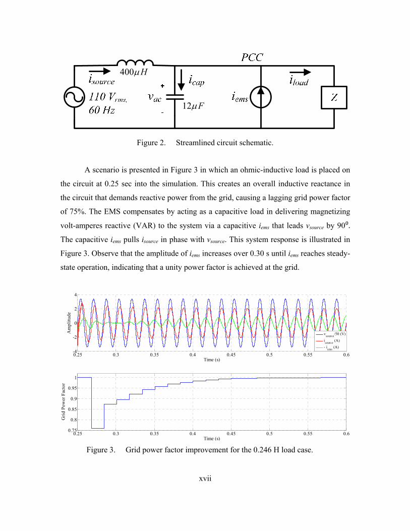
Figure 2. Streamlined circuit schematic.
A scenario is presented in Figure 3 in which an ohmic-inductive load is placed on
the circuit at 0.25 sec into the simulation. This creates an overall inductive reactance in
the circuit that demands reactive power from the grid, causing a lagging grid power factor
of 75%. The EMS compensates by acting as a capacitive load in delivering magnetizing
volt-amperes reactive (VAR) to the system via a capacitive iems that leads vsource by 90⁰.
The capacitive iems pulls isource in phase with vsource. This system response is illustrated in
Figure 3. Observe that the amplitude of iems increases over 0.30 s until iems reaches steady-
state operation, indicating that a unity power factor is achieved at the grid.
Figure 3. Grid power factor improvement for the 0.246 H load case.
0.25 0.3 0.35 0.4 0.45 0.5 0.55 0.6-4
-2
0
2
4
Time (s)
Am
plit
ude
vsource
/50 (V)
isource
(A)
- iems
(A)
0.25 0.3 0.35 0.4 0.45 0.5 0.55 0.60.75
0.8
0.85
0.9
0.95
1
Time (s)
Gri
d Po
wer
Fac
tor

xviii
It is important to note that iems is displayed in Figures 3 to satisfy the passive
sign convention. The passive sign convention dictates that the reference direction for
positive current flow is into a load; however, the simulation treats the EMS as a source
whereby iems flows out of the EMS as shown in Figure 2. Hence, −iems is presented in the
results to show the positive flow of current into the EMS, which is consistent with the
reference direction used to describe the positive flow of current to all other loads.
To validate the simulation results, an experiment was conducted for the same load
scenario. The EMS was encoded to run the Simulink program, and the ohmic-inductive
load was placed on the EMS to replicate the aforementioned simulation scenario. The
results of the experiment are shown in Figures 4 and 5.
The EMS was not turned on at the start of the experiment so that the effects of the
inductive power demand on the grid could be observed. Note in Figure 4 that the ohmic-
inductive load creates a lagging power factor at the grid since isource lags vsource by
approximately 30⁰, which translates into an 87% source power factor. The power factor
inconsistency between the two trials is expected since the simulation neglects the many
electronic devices that induce reactance within the circuit..
Figure 4. Source voltage and current when EMS current is off.
-0.02 -0.015 -0.01 -0.005 0 0.005 0.01 0.015 0.02-4
-3
-2
-1
0
1
2
3
4
Time (s)
Am
plit
ude
vsource
/50 (V)
isource
(A)
- iems
(A)

xix
Once the EMS is turned on, capacitive power is delivered to the system via a
leading iems, causing the phase angle of isource to slightly lead vsource as shown in Figure 5.
This over-compensation of reactive power to the grid occurs because the EMS does not
currently possess a sensor on the source current and is, therefore, incapable of conducting
closed-loop current control of emsi . The Simulink code commands the EMS to adjust the
amplitude of injected emsi until a unity power factor is achieved, but the EMS cannot
adjust the amplitude of emsi without the use of a proportional-integral (PI) controller.
Hence, the EMS merely produces a steady 1.0 A peak (or Apk) sinusoidal emsi signal in
quadrature with the source voltage, which forces the EMS to over-compensate in selling
reactive power to the grid. Adding a source current sensor to the EMS is a planned
hardware upgrade that should remedy the issue.
Observe in Figure 5 the obvious presence of harmonics in the emsi signal. These
harmonic signatures occur as a result of the PWM switching scheme used by the EMS to
generate the iems signal. They are not evident in the simulation results since the circuit
modeled in Simulink disregards the PWM associated with the EMS’s power electronics.
Figure 5. Source voltage and current when EMS current is on.
-0.02 -0.015 -0.01 -0.005 0 0.005 0.01 0.015 0.02-4
-3
-2
-1
0
1
2
3
4
Time (s)
Am
plit
ude
vsource
/50 (V)
isource
(A)
- iems
(A)

xx
The ability of the EMS to operate as a current source in compensating for a
reactive power demand on the grid was successfully demonstrated in this thesis. The
method utilized a power factor improvement process developed in Simulink. Specifically,
a zero-crossing detection algorithm tracked the power factor angle between the source
voltage and current so that an appropriate amount of reactive current can be injected into
the system at the PCC in order to achieve a unity power factor at the grid. The process
was simulated to predict the system’s response to capacitive and inductive power
demands on the grid. A laboratory experiment was then conducted with the actual EMS
to validate the process.
The results built confidence in the ability of the EMS to compensate for a reactive
power demand on the grid; however, improving the simulation and experiment could
potentially facilitate a better understanding of the EMS’s capabilities. For example, the
experiment should be repeated once a current sensor is added on the source. Also, the
simulation could be further developed to model the EMS’s power electronics architecture
to include the PWM and controller required to operate the H-bridge inverter. Combining
the two aforementioned efforts into a single project might provide for a better comparison
of the simulation and experimental results.

xxi
ACKNOWLEDGMENTS
Much thanks to Professors Alex Julian and Giovanna Oriti for making this thesis
a painless yet worthwhile experience.

xxii
THIS PAGE INTENTIONALLY LEFT BLANK

1
I. INTRODUCTION
A. BACKGROUND
The Department of Defense (DOD) has identified department-wide goals for
increasing energy efficiency and reducing energy costs both on the battlefield and across
its installations. In particular, the United States Marine Corps (USMC) and Department
of the Navy (DON) seek to make 50% of all installations net-zero energy efficient and
require that 50% of all energy consumption aboard installations come from alternative
energy sources by 2020 [1]. These goals imply that the DON and USMC must pursue
suitable energy management practices and technologies in addition to transitioning to
alternative fuels in order to improve energy efficiency and reduce cost at installations.
A significant contributor to higher energy costs and reduced energy efficiency is
the overall inductive power demand on the bulk electric grid by both DOD and civilian
consumers. This inductive power demand reduces the power factor (PF) on the supply
side of an electrically coupled power network, which creates numerous challenges to
generating, transmitting, and distributing electric power to the consumer. These
challenges are well-known and include voltage and power losses (reduced power
efficiency) along transmission lines and in transformers, limited real (active) power
supplied to the consumer, and higher energy and installation costs due to increased power
rating requirements on generators and power distribution infrastructure necessary to
support high reactive loads [2]. Transmission line length also affects cost since line losses
vastly increase when power is transmitted over significant distances to the consumer [2].
This is often the case in California where power is commonly shipped from neighboring
states. These costs are eventually passed on to the consumer. Along with ensuring energy
security at installations [1], reducing energy costs is one of the foremost reasons why the
DOD requires each net-zero energy installation to “produce as much energy on or near
the installation as it consumes in its buildings and facilities” [3].
An example of reactive power costs charged directly to a commercial consumer in
the UK is shown in Figure 1. Note that the installation was charged a fixed rate for a peak

2
load of 850 kVA. Real and reactive energy consumption was charged at assigned per
unit rates; although, reactive power was charged at a much lower rate of 0.271 pence
(0.45 cents) per kVARh (volt-ampere reactive hour). The installation’s average power
factor during the period was relatively high at 0.949 or 94.9% [2].
UK power bill, from [2]. Figure 1.

3
Commercial consumers in the United States typically are not charged directly for
reactive power consumption. Instead, they are charged for their real power usage at
higher peak and off-peak rates than in the UK and assessed a rebate for reactive power
savings resulting from a high average power factor during the billing cycle. This practice
is demonstrated by the Pacific Gas and Electric (PG&E) power bill for Naval
Postgraduate School (NPS) in Monterey, California, shown in Figure 2. Note that NPS
received a $458.21 rebate based on a power factor of 0.93 or 93%. The bill is split into
two parts due to a utility rate change that occurred during the billing period.
PG&E power bill for NPS. Figure 2.

4
From a comparison of Figures 1 and 2, it is apparent that energy cost savings can
be achieved by compensating for reactive power, which directly relates to power factor
improvement. The power factor is a measure of power efficiency and, therefore, plays an
important role in understanding reactive power compensation. The power factor describes
how efficiently a supply delivers real power to a load and is mathematically defined as
PF=cos ( ) (1)
where the power factor angle v i is the difference between the voltage and current
phase angles. A unity power factor (i.e., PF = 1) implies that a sinusoidal voltage and
current are in phase (i.e., v i ), which yields maximum real power flow since the
relationship between power factor and real power P is given by
v iP=V I cos ( - ) (2)
where voltage V and current I are the root mean square (RMS) values of the voltage and
current. Conversely, a unity power factor implies no reactive power flow since reactive
power Q is given by
v iQ=V I sin -( ). (3)
Hence, achieving a unity power factor at a desired location in a circuit is the objective in
reducing reactive power flow at the same point.
In addition to creating energy cost savings, reactive power compensation
increases energy efficiency gains. As previously discussed, transmission lines bleed
reactive power more quickly than real power, which increases power losses and reduces
power efficiency along the transmission lines—especially over long distances [4]. Also,
most consumer loads are inductive in nature. The current of an inductance lags the
voltage resulting in a lagging power factor, which tends to lower the system voltage [4]
by drawing reactive energy from the system. As such, inductive loads typically cause
voltage sags along transmission lines that limit the delivery of real power to the
consumer. Conversely, the current of a capacitance leads the voltage resulting in a
leading power factor, which tends to raise the system voltage [4] by delivering reactive
energy to the system. Providing capacitive power support to the power distribution
system, therefore, reduces power losses and improves voltage quality along transmission

5
lines [4]. Transmitting reactive power also increases the amount of RMS current in the
transmission lines, which results in additional line losses since 2lossP I R . Hence,
reducing reactive power demand likewise enhances the delivery of real power to the
consumer since current otherwise wasted in power loss or transmitting reactive power is
used to transmit real power.
The compensation of reactive power ideally occurs as close to the inductive load
as possible in order to eliminate the need for reactive power support from the grid by
achieving a unity power factor [2]. This typically happens at the point of common
coupling (PCC) in an electrically coupled distribution network. By providing
compensating reactive power at the PCC, power lines from the supplier to the consumer
are loaded only with active energy supplied by the grid [2]. Compensating to a less-than-
unity power factor requires additional reactive power support from the grid, which further
burdens feed-in lines to the consumer and reduces energy efficiency as a result of energy
losses in transmission [2].
There are many common ways to compensate for inductive power. Most of these
are not discussed in this thesis; however, the use of an energy management system (EMS)
to control reactive power in a system is investigated. EMS applications in power
electronics are becoming increasingly popular. An EMS can monitor reactive power
requirements in an electrical circuit and inject reactive power when and where necessary
in a circuit to increase energy efficiency within a system or limit the reactive power
supply burden on the bulk electric grid and distributed generation (DG) sources. The
EMS investigated in this thesis is described in more detail in the next chapter.
B. OBJECTIVE
The purpose of this thesis is to demonstrate the capability of an EMS to
compensate for a reactive power demand on the grid. This is accomplished by first using
zero-crossing detection to determine the source power factor angle φsource between the
source voltage and current. The appropriate amount of reactive power is then injected
into the system using the EMS as a reactive current source in order to achieve a unity
power factor at the grid. Although the power factor improvement of a single-phase grid is

6
investigated in this thesis, the EMS can provide the same capability to three-phase
systems.
C. APPROACH
In order to adequately demonstrate the ability of the EMS to facilitate reactive
power compensation and achieve a unity power factor at the source, the first step was to
model the EMS with zero-crossing detection capability and closed-loop current control
using Simulink software [5]. Varying loads were scheduled in the simulation to show the
capability of the EMS to compensate for a changing reactive power demand on the grid.
The Simulink model was streamlined in order to better isolate the zero-crossing detection
feature of the EMS for the purpose of simplifying data collection and analysis. Certain
model subsystems deemed unnecessary or extraneous for the purpose of this thesis were
removed.
Finally, a laboratory experiment was conducted using the EMS. The Simulink
model was compiled into code that commanded the EMS to operate as a current source in
compensating reactive power using zero-crossing detection. Experimental data was
collected and compared to the simulation results.
D. PREVIOUS WORK
Much research involving the EMS discussed in this paper has been conducted to
date. Previous Naval Postgraduate School students have added capabilities to the EMS
over the years thereby evolving it into the current system. Recent work includes
designing the EMS to choose between two different generators and a battery bank to
power loads typically found at a forward operating base with the goal of improving fuel
efficiency [6]. The ability of the EMS to store unused energy in the battery bank and
disable generator power during periods of light loading [6] is also demonstrated. Other
works include an analysis of the effects on microgrid power quality given different H-
bridge inverter loading schemes [7] and using the EMS to manage peak power demand
on a microgrid in order to improve energy efficiency and reduce energy costs [8].

7
While the addition of a reactive power compensation capability to the EMS is
discussed in this thesis, reactive power compensation using energy management systems
is not a new concept. In one particular IEEE Industry Applications Magazine article, the
authors investigate via simulation the addition of decision-making ability to a
multifunctional single-phase voltage-source inverter (VSI) [9]. The inverter possesses the
same smart functionalities as the EMS studied in this thesis. Specifically, the authors
demonstrate the VSI’s ability to select from various modes of operation in response to
certain system conditions or electricity pricing.
In one particular case, the inverter detects a voltage sag at the grid, which is
created by the reactive power demand of two VSI loads. The inverter then schedules
reactive power to the PCC to alleviate the voltage sag [9]. The result is shown in Figure
3. Note that the voltage sag is created at 0.5 s. The inverter immediately compensates,
and the voltage sag is corrected after 1.2 s. However, the inverter continues to sell
reactive power to the grid, causing a spike in grid voltage. The inverter’s static
synchronous compensator function then absorbs the excess reactive power causing the
grid voltage to stabilize [9].
Per unit grid voltage magnitude, from [9]. Figure 3.
In another paper, the authors demonstrate closed-loop current control in utilizing
DG unit “interfacing converters to actively compensate harmonics” [10]. A cost-effective

8
solution whereby fundamental and harmonic DG currents are independently controlled
without the need for current detection in the load or voltage detection in the distribution
system is proposed [10]. The authors also use a simple closed-loop power control method
to detect the fundamental current reference without the use of phase-locked loops thereby
avoiding fundamental current tracking errors [10]. A similar closed-loop control
facilitating reactive power control is later demonstrated in this thesis.

9
II. ENERGY MANAGEMENT SYSTEM
A. FUNCTIONALITY
The EMS utilized in this thesis is designed as an enabling technology capable of
providing digitally-controlled “smart grid” functionality to electrical power consumers by
facilitating power flow control to the consumer while simultaneously increasing power
reliability and improving energy system security [11]. Depending on the situation, the
EMS can act as a voltage source or a current source either while connected to a main AC
source such as a bulk power grid or independent of the grid in islanded mode using
various DG sources (photovoltaic panels, fuel cells, gas generators, batteries, etc.).
Moreover, the EMS possesses an energy storage capability currently in the form
of a lead-acid battery bank [11]. The following list details the major functions of
the EMS [11]:
User interfacing to facilitate selective functionality.
Real and reactive power tracking and control.
Peak power management.
Power quality control and reliability enhancement.
Load scheduling and management to include non-critical load shedding and critical load maintenance.
Source power management to include DG source application.
Energy storage management.
Fault detection and correction.
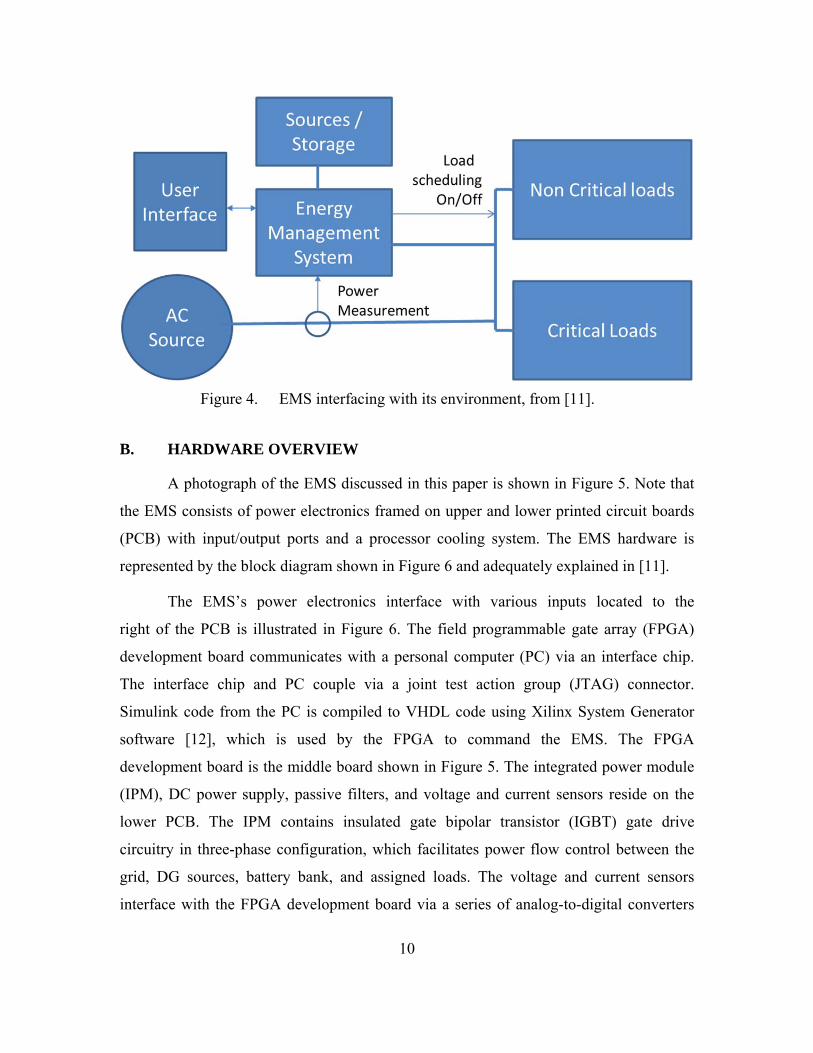
A block diagram demonstrating how the EMS might interface with its
environment is provided in Figure 4. Note that the EMS integrates DG sources and
storage capabilities to support various loads based on priorities established by the
consumer. Ideally, the EMS provides power support to the grid unless a specified power
management scenario calls for autonomous operation as previously discussed.
10
EMS interfacing with its environment, from [11]. Figure 4.
B. HARDWARE OVERVIEW
A photograph of the EMS discussed in this paper is shown in Figure 5. Note that
the EMS consists of power electronics framed on upper and lower printed circuit boards
(PCB) with input/output ports and a processor cooling system. The EMS hardware is
represented by the block diagram shown in Figure 6 and adequately explained in [11].
The EMS’s power electronics interface with various inputs located to the
right of the PCB is illustrated in Figure 6. The field programmable gate array (FPGA)
development board communicates with a personal computer (PC) via an interface chip.
The interface chip and PC couple via a joint test action group (JTAG) connector.
Simulink code from the PC is compiled to VHDL code using Xilinx System Generator
software [12], which is used by the FPGA to command the EMS. The FPGA
development board is the middle board shown in Figure 5. The integrated power module
(IPM), DC power supply, passive filters, and voltage and current sensors reside on the
lower PCB. The IPM contains insulated gate bipolar transistor (IGBT) gate drive
circuitry in three-phase configuration, which facilitates power flow control between the
grid, DG sources, battery bank, and assigned loads. The voltage and current sensors
interface with the FPGA development board via a series of analog-to-digital converters

11
located on the upper PCB. Also located on the upper PCB is a transistor-to-transistor
interface used to command power from assigned DG sources and manage various loads.
Finally, an LCD shows desired feedback information to the user.
Photograph of the EMS analyzed in this thesis. Figure 5.
EMS interfacing diagram. Figure 6.

12
C. MODELING APPROACH
As previously discussed, the objective of this paper is to demonstrate the
capability of the EMS to compensate for a reactive power demand on the source by
injecting the appropriate amount of compensating reactive current into the system at the
PCC. This capability is described in detail in the following chapter; however, it is
important to understand the method for modeling this process in this thesis and how it
differs from actual EMS functionality.
A schematic demonstrating the means by which the IPM interfaces critical and
non-critical loads with AC and DC power supplies is provided in Figure 7. The EMS uses
a single-phase H-bridge inverter consisting of two single-leg inverters, which is preferred
over other inverter types in high power applications [13]. A third leg connects a DC
power supply to the H-bridge inverter via a buck-boost DC-to-DC converter. A pulse
width modulation (PWM) scheme with unipolar voltage switching delivers the H-bridge
gate signals [7] and reduces the effects of harmonics in the output voltage at the
switching frequency [13]. A low-pass LC filter (LPF) facilitates a clean AC signal at the
output of the inverter. The LPF is shown in Figure 7. Note that the filter capacitor is
marked by vac, and reactive current iems flows through the filter inductor.
+
- vac
vdc
iems
+
vbatt-
+
-
Critical loads
Noncritical loads
ACgrid
Controller
Buckswitch
Boostswitch
H-bridge
iload
idc
isource
12 F
EMS
EMS power electronics circuit schematic. Figure 7.

13
Recall that the H-bridge inverter can be controlled as a current source or a voltage
source. For the purpose of this thesis, the H-bridge inverter is controlled as a current
source using a programmable microcontroller. The microcontroller provides a number of
control features to the EMS. In particular, it regulates the polarity of the output voltage
from the H-bridge inverter by controlling the H-bridge inverter’s IGBT switches and
controls the flow of power using feedback provided by a sensor positioned at the load.
This control scheme is shown in Figure 7.
As a current source, the EMS produces an output current iems, which is used to
inject compensating reactive power at the PCC. A particular method for controlling iems in
providing reactive power support to the AC grid is demonstrated in this thesis. This
method involves using a Simulink-based zero-crossing detection algorithm to determine
the power factor angle φsource at the grid and, subsequently, changing the amplitude of the
compensating reactive current iems to bring φsource to zero. Achieving a unity power factor
at the source eliminates reactive power demand on the grid.
To effectively model this process, an equivalent of the circuit shown in Figure 7 is
simulated using Simulink software. The reason for using an equivalent circuit is to
demonstrate the EMS as a constant current source in order to examine the use of iems in
compensating for a reactive power demand on the AC grid. A schematic of the idealized
circuit is illustrated in Figure 8. Modeling the EMS in this fashion assumes a clean
sinusoidal iems signal from the H-bridge inverter without having to consider pulse width
modulation and associated closed-loop voltage control to produce the iems necessary to
achieve a unity power factor at the grid.
iload
Zvac
+
-
iems
isource icap
PCC
12 F
400 H
110 Vrms,
60 Hz
Idealized circuit schematic. Figure 8.

14
Notice from Figure 8 that the EMS block in Figure 7 is effectively eliminated
from the idealized circuit. All circuitry to the left of the 12 µF filter capacitor in Figure 7
is not considered in the schematic in Figure 8 except for the flow of iems from the EMS to
the PCC. This idealized modeling scheme facilitates a more focused examination of the
power factor improvement methodology developed for the EMS using Simulink, which is
explained in detail in Chapter III.
The experimental EMS of course remains as shown in Figure 7 and, therefore,
employs pulse width modulation to create the H-bridge gate signals that generate a
voltage to control iems. The power factor improvement methodology developed in
Simulink still applies to the experiment, but no proportional-integral (PI) controller was
implemented in the lab to correct iems because the EMS hardware currently does not have
a sensor on the source current. Adding a sensor to the source current is a planned upgrade
to the system. Due to this restraint, the experiment was conducted without the use of
closed-loop current control, but the EMS still demonstrated the capability to generate
compensating reactive current in response to a reactive power demand on the grid. The
results are explained in further detail in Chapter IV.

15
III. COMPUTER SIMULATION
A. OVERVIEW
A computer simulation of the idealized circuit shown in Figure 8 was created
using Simulink. The simulation design is based on the circuit shown in Figure 9, which is
the same circuit presented in Figure 8 except with two defined variable loads tested
both in simulation and experiment. Load 1 is a purely resistive 85.7 Ω load. Load 2 is a
0.246 H inductive load with an estimated internal resistance of 5 Ω. The purpose of the
two loads is to demonstrate the capability of the EMS to compensate for a varying
reactive power demand on the grid.
ACgrid vac
+
-
EMS
iemsisource
iloadicap
PCC
5 Ω
0.246 H
Load 2
Load 1
85.7 Ω
12 μF
400 μH
Circuit schematic replicated in simulation. Figure 9.
The circuit is mathematically simulated by the circuit component and subsystem
diagram in Figure 10. The 12 µF filter capacitor and 400 µH filter inductor with 10 mΩ
resistance are clearly displayed in the diagram as independent of the subsystems. A
constant 110 Vrms, 60 Hz sinusoidal input signal from the grid precedes the filter inductor.
The Load Switching subsystem contains both variable loads, which are controlled by an
electronic switch that adds inductance to the system at a predetermined time in the
simulation. The Power Factor Correction subsystem contains the zero-crossing detection

16
and power factor angle error correction algorithms used to continuously track phase
angles of vsource and isource (sourcev and
sourcei , respectively) and subsequently determine and
correct power factor angle φsource in order to achieve a unity power factor at the grid. The
Power Factor Correction subsystem also employs closed-loop current control, which
drives φsource to zero by changing the amplitude of iems as it flows to the PCC.
Simulink circuit component and subsystem diagram. Figure 10.
To keep the model as visually clean as possible, all circuit data regarding output
variables 1 through 11 (depicted in Figure 10) is sent to the top-level block diagram
shown in Figure 11. There it is collected along with simulation time and sent to the
MATLAB “workspace” for graphical analysis. The MATLAB file scripts containing the

17
system’s initial conditions, discrete component values, and code used to create the plots
in this thesis are presented in the Appendix.
Simulink top-level block diagram. Figure 11.
B. LOAD SWITCHING
As previously stated, load switching is used to demonstrate the capability of the
EMS to compensate for a varying reactive power demand on the grid. The resistive and
inductive loads shown in Figure 9 are simulated using the load switching subsystem
presented in Figure 12. At the start of the simulation, only the 85.7 Ω load is active,
which results in an overall capacitive reactance in the circuit due to the dominating
presence of the 12 µF low-pass filter capacitor in the circuit. The result is an overall
capacitive power demand on the source that is quickly compensated by the injection of
inductive iems at the PCC.
At 0.25 s into the simulation, the 0.246 H inductive load with 5 Ω internal
resistance is added to the circuit. The load switching operation is controlled by the load

18
step and Switch1 function blocks shown in Figure 12. This new load scheme creates an
overall inductive power demand on the grid that models the power demand of a typical
reactive power consumer. A capacitive iems is accordingly injected at the PCC to correct
the lagging power factor produced at the grid by the inductive load. The results are
presented in Section D of this chapter.
Simulink load switching subsystem diagram. Figure 12.
C. POWER FACTOR CORRECTION
The method used to create a unity power factor at the source is conceptually
simple. The power factor correction flow chart shown in Figure 13 illustrates the process.
First, the source power factor angle φsource is calculated using zero-crossing detection. As
φsource is gradually driven to zero via closed-loop control, it is passed through a simple
first-order, low-pass filter transfer function. The LPF filter softens the change in φsource
over time, which assists the PI controller in smoothly adjusting reference current
amplitude *emsI . The EMS concurrently generates a continuous 1.0 Apk sinusoidal current
in quadrature with the sinusoidal source voltage that is multiplied with *emsI to create the
sinusoidal EMS reference current *emsi . The reference current *
emsi is designed to lead

19
vsource by 90⁰ when isource lags vsource so that *emsi improves the power factor at the grid
when injected into the system. Alternatively, the reference current amplitude *emsI will be
negative so that the injected *emsi lags vsource by 90⁰ in order to improve a leading grid
power factor.
Conceptually, *emsi is then compared to the measured EMS output current emsi per
the flow chart. The difference between the two waveforms defines the error that is
corrected by another PI controller, which directs the inverter to generate a new emsi via
changes in the PWM scheme until emsi = *emsi . At this point, the system makes no further
changes to emsi since a unity power factor is realized at the grid. Recall that the
experimental EMS currently lacks a sensor at the source, and it is not yet possible to use
closed-loop control to makes changes to the actual PWM in the laboratory. The results of
the experiment are discussed in Chapter IV.
x
Sine
H-bridgegate signalsPI PWM
+-2
emsi
+-
sourcev +-
sourcei
PI*emsI
*emsi
LPF
sin 2
sourcev
sourcev
source
Power factor correction flow chart. Figure 13.
Recall from Figures 8 and 9 that the Simulink model does not account for PWM
in the EMS and, therefore, does not create an emsi signal. The simulation instead
simplifies the power factor correction process by assuming that *emsi = emsi and, thus, only
adjusts *emsi as necessary to correct the source power factor. Accordingly, *
emsi feeds
continuously into the PCC and is regulated via the first PI controller shown in Figure 13
as φsource changes over time.

20
The function of the power factor correction diagram shown in Figure 14 is to
implement the power factor correction flow chart in Figure 13 using Simulink. The
components and subsystems that comprise the power factor correction block are
illustrated by the Simulink power factor correction subsystem diagram in Figure 14. Note
that the diagram replicates all flow chart functions leading to the creation of the *emsi
signal. The PI controller and quadrature reference current signal are contained within the
closed-loop current control subsystem. All parameter data is sent to the output of the
power factor correction diagram to include emsi , which is then injected back into the PCC
as demonstrated in Figure 10.
Simulink power factor correction subsystem diagram. Figure 14.
1. Zero-Crossing Detection
In order to determine the source power factor angle φsource, the EMS uses zero-
crossing detection algorithms to determine phase angles sourcev and
sourcei . These
algorithms are located in the source voltage and source current Zero-Crossing Detection
subsystems illustrated in Figure 14. The algorithm for determining sourcev is less complex

21
since vsource remains constant. The Simulink vsource zero-crossing detection algorithm for
determining sourcev is shown in Figure 15.
Simulink source voltage zero-crossing detection diagram. Figure 15.
The algorithm detects the positive rise of vsource by determining if the present
sinusoidal voltage input value is positive and the previous value is non-positive. If a
positive rise is detected, the Detect Positive Rise function block outputs a Boolean
TRUE. Otherwise, the block outputs a Boolean FALSE. A TRUE statement signifies that
the signal crossed the time axis while rising, which occurs once every cycle for a
sinusoidal signal. The Integrator function block integrates over time t of the source
voltage signal frequency from zero to a reset time of period T and then repeats. The
integrator is programmed to reset when the Detect Positive Rise function block outputs a
Boolean TRUE (i.e., detects a positive rise across the time axis). The result gives the
phase angle by the relationship
0
2T
fdt (4)
where the period T is the time between successive positive rises across the time axis and
f is the signal frequency, which is typically 60 Hz for the grid voltage.
The EMS computes sourcei using an algorithm similar to that of
sourcev except the
isource zero-crossing detection algorithm compares each integrator output value of sourcei to
the quantity 1.6π. The algorithm ensures that the present value of sourcei is greater than
1.6π during a positive rise before reporting a Boolean TRUE to the Integrator function
block. This prevents the integrator from prematurely resetting in the event that signal

22
transients or disturbances in isource cause the signal to unexpectedly perform a zero-
crossing. This process is demonstrated by the Simulink diagram in Figure 16.
Simulink source current zero-crossing detection diagram. Figure 16.
Source voltage and current phase angle plots for both load cases. Figure 17.
Plots showing the change in sourcev and
sourcei over time for both the resistive and
inductive load cases are presented in Figure 17. The graphic only shows the first 0.35 s of
the simulation for the purpose of visual acuity. As previously mentioned, an overall
capacitive reactance initially exists in the circuit before adding the inductive impedance
to the load resulting in a leading power factor since isource leads vsource. Once the inductive
0 0.01 0.02 0.03 0.04 0.05 0.06 0.07 0.08 0.09 0.10
100
200
300
400Resistive Load (85.7 )
Time (s)
Pha
se A
ngle
, (
deg)
v
source
isource
0.25 0.26 0.27 0.28 0.29 0.3 0.31 0.32 0.33 0.34 0.350
100
200
300
400
500Inductive Load (0.246 H) Added to the Circuit at t = 0.25 s
Time (s)
Pha
se A
ngle
, (
deg)
v
source
isource

23
load is introduced, the circuit experiences an overall inductive reactance, which causes
isource to lag vsource and results in a lagging power factor. Notice that the simulation
gradually brings isource in phase with vsource for both load cases since the simulation is
running the power factor correction algorithm in the example.
2. Power Factor Angle Error Correction
The phase difference between sourcev and
sourcei is then computed to determine the
source power factor angle φsource by subtracting the two quantities via the Add5 block
shown in the Power Factor Correction subsystem in Figure 14; however, computing
φsource in this fashion results in numerical errors. The errors are caused by the
asynchronous resetting of the Integrator function blocks in Figures 15 and 16 in
computing sourcev and
sourcei , respectively, using zero-crossing detection.
This mathematical glitch is best understood from Figure 17. In the inductive load
case, for example, isource lags vsource allowing the sourcev integrator to wrap from 2π to zero
before the sourcei integrator. The result is a momentarily large φsource that abruptly declines
as φsource approaches zero. These errors are displayed as spikes in the power factor
calculation plot shown in Figure 18 and must be eliminated before closed-loop current
control can operate to pull isource in phase with vsource.
Power factor calculation with numerical integration error. Figure 18.
0 0.1 0.2 0.3 0.4 0.5 0.6-400
-300
-200
-100
0
100
200
300
400
Time (s)
Cal
cula
ted
PF
Ang
le,
(de
g)

24
The Power Factor Angle Error Correction subsystem shown in Figure 19
eliminates the numerical error in φsource simply by adding 2π to φsource if φsource is less than
π or subtracting 2π from φsource if φsource is greater than π. This arithmetical process is
possible since the calculated error in φsource cannot be greater than ±2π simply because
φsource cannot mathematically be more than ±2π as demonstrated by the error spikes in
Figure 18; hence, numerical error nears ±2π as φsource approaches zero. Note in Figure 18
that the power factor angle is plotted in degrees instead of radians.
Simulink power factor angle error correction diagram. Figure 19.
The corrected power factor angle is then passed through a simple first-order low-
pass filter transfer function as seen in Figure 14. The LPF softens the change in φsource
over time, which assists the Closed-Loop Current Control subsystem in smoothly
adjusting the reference current amplitude *emsI . Plots of the corrected and filtered power
factor angle are shown in Figure 20. Note from the plots that φsource < 0 when the circuit
is capacitive (0 s < time < 0.25 s) and φsource > 0 when the circuit is inductive (time > 0.25
s). The load change is scheduled at precisely 0.25 s; however, the zero-crossing detection
algorithm does not detect a change in sourcei until the end of the next zero-crossing event,
which occurs one full period (1/60 s) later.

25
Corrected and filtered power factor angle plots. Figure 20.
3. Closed-Loop Current Control
The function of the Simulink Closed-Loop Current Control subsystem is to
modify EMS output current *emsi by changing its amplitude *
emsI . The closed-loop current
control block diagram is shown in Figure 21. The diagram mathematically replicates the
*emsi generation process described by the flow chart in Figure 13.
Simulink closed-loop current control diagram. Figure 21.
0 0.1 0.2 0.3 0.4 0.5 0.6-40
-20
0
20
40
60
Time (s)
Cor
rect
ed P
F A
ngle
, (
deg)
0 0.1 0.2 0.3 0.4 0.5 0.6-40
-20
0
20
40
60
Time (s)
Fil
tere
d P
F A
ngle
, (
deg)

26
EMS current amplitude *emsI is produced as the output of the PI controller. The
controller uses negative feedback to drive φ to zero. The fed-back output signal is
reactive current *emsi , which is created by multiplying *
emsI with a 1.0 Apk continuous
sinusoidal waveform generated in quadrature with vsource. The fed-back output signal thus
has the form
* * sin 2sourceems ems vi I (5)
where amplitude *emsI is adjusted by the PI controller to bring isource in phase with vsource.
Changing the phase angle of isource by adjusting the amplitude of *emsi is possible
by Kirchhoff’s Current Law (KCL). This is apparent when observing the flow of current
through the PCC of the circuit in Figure 9. Given that *emsi = emsi for the simulation
circuit, the KCL equation for isource is
source load cap emsi i i i (6)
where positive emsi describes the flow of EMS current into the PCC, hence the minus
sign in Equation (6).
Plots of *emsI and φsource versus time are displayed in Figure 22. The plots
demonstrate the relationship between *emsI and φsource—specifically how EMS current
amplitude *emsI changes accordingly to pull isource in phase with vsource (i.e., force φsource to
zero) thereby achieving a unity power factor at the grid. Also note that *emsI approaches
unity as φsource approaches zero. This occurs because no further change to *emsi is required
when φsource = 0. Observe that *emsI can be negative or positive depending on whether
isource leads or lags vsource, respectively.
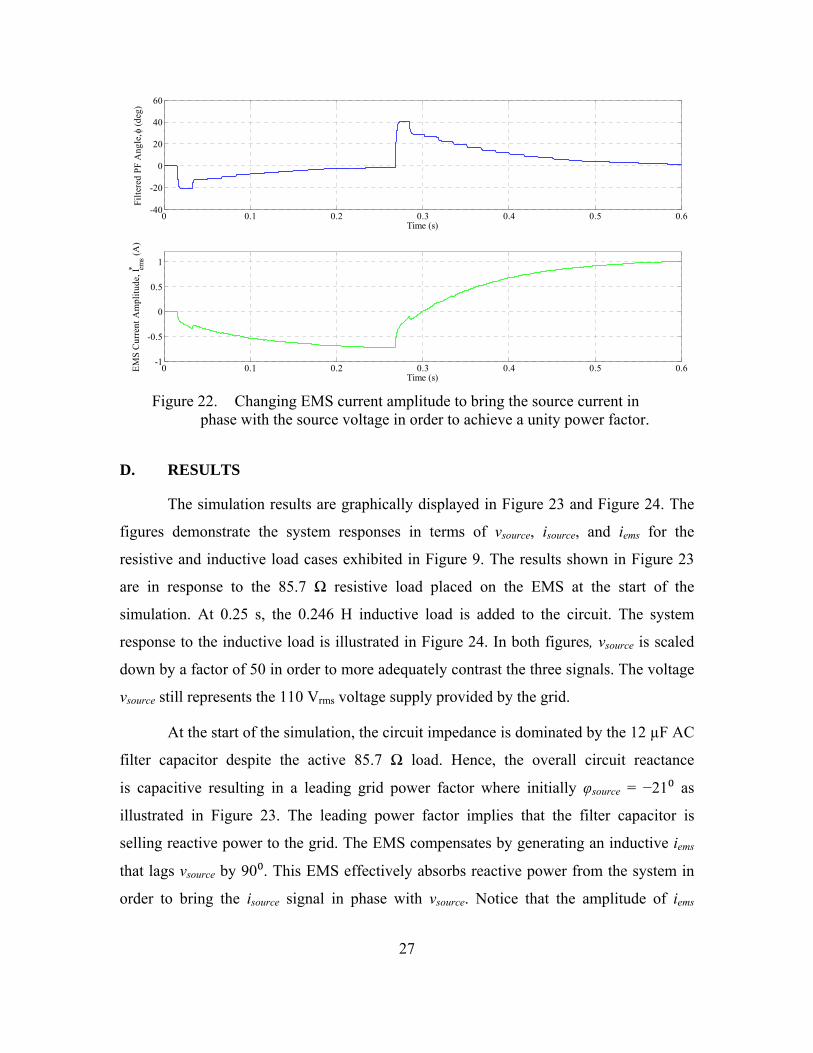
27
Changing EMS current amplitude to bring the source current in Figure 22. phase with the source voltage in order to achieve a unity power factor.
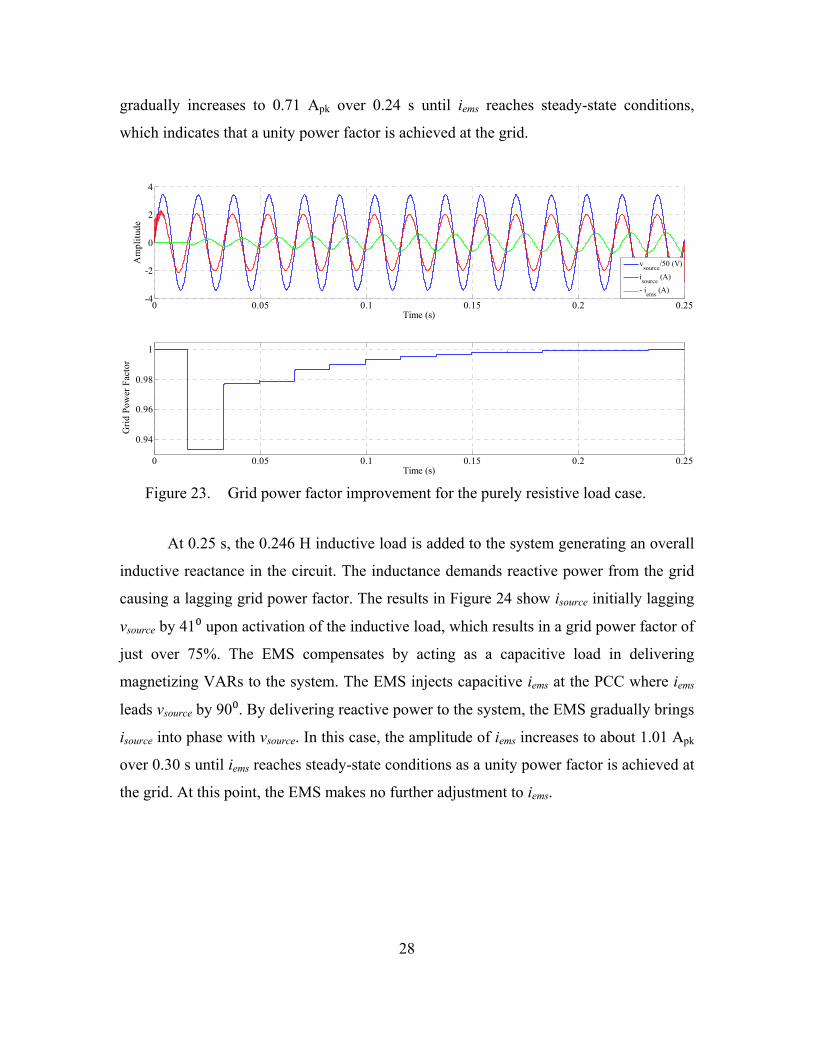
D. RESULTS
The simulation results are graphically displayed in Figure 23 and Figure 24. The
figures demonstrate the system responses in terms of vsource, isource, and iems for the
resistive and inductive load cases exhibited in Figure 9. The results shown in Figure 23
are in response to the 85.7 Ω resistive load placed on the EMS at the start of the
simulation. At 0.25 s, the 0.246 H inductive load is added to the circuit. The system
response to the inductive load is illustrated in Figure 24. In both figures, vsource is scaled
down by a factor of 50 in order to more adequately contrast the three signals. The voltage
vsource still represents the 110 Vrms voltage supply provided by the grid.
At the start of the simulation, the circuit impedance is dominated by the 12 µF AC
filter capacitor despite the active 85.7 Ω load. Hence, the overall circuit reactance
is capacitive resulting in a leading grid power factor where initially φsource = −21⁰ as
illustrated in Figure 23. The leading power factor implies that the filter capacitor is
selling reactive power to the grid. The EMS compensates by generating an inductive iems
that lags vsource by 90⁰. This EMS effectively absorbs reactive power from the system in
order to bring the isource signal in phase with vsource. Notice that the amplitude of iems
0 0.1 0.2 0.3 0.4 0.5 0.6-40
-20
0
20
40
60
Time (s)
Filt
ered
PF
Ang
le,
(de
g)
0 0.1 0.2 0.3 0.4 0.5 0.6-1
-0.5
0
0.5
1
Time (s)
EM
S C
urre
nt A
mpl
itud
e, I* em
s (A
)
28
gradually increases to 0.71 Apk over 0.24 s until iems reaches steady-state conditions,
which indicates that a unity power factor is achieved at the grid.
Grid power factor improvement for the purely resistive load case. Figure 23.
At 0.25 s, the 0.246 H inductive load is added to the system generating an overall
inductive reactance in the circuit. The inductance demands reactive power from the grid
causing a lagging grid power factor. The results in Figure 24 show isource initially lagging
vsource by 41⁰ upon activation of the inductive load, which results in a grid power factor of
just over 75%. The EMS compensates by acting as a capacitive load in delivering
magnetizing VARs to the system. The EMS injects capacitive iems at the PCC where iems
leads vsource by 90⁰. By delivering reactive power to the system, the EMS gradually brings
isource into phase with vsource. In this case, the amplitude of iems increases to about 1.01 Apk
over 0.30 s until iems reaches steady-state conditions as a unity power factor is achieved at
the grid. At this point, the EMS makes no further adjustment to iems.
0 0.05 0.1 0.15 0.2 0.25-4
-2
0
2
4
Time (s)
Am
plit
ude
vsource
/50 (V)
isource
(A)
- iems
(A)
0 0.05 0.1 0.15 0.2 0.25
0.94
0.96
0.98
1
Time (s)
Gri
d P
ower
Fac
tor

29
Grid power factor improvement for the inductive load case. Figure 24.
It is important to note that −iems is used to represent EMS current in the simulation
results shown in Figure 23 and Figure 24 in order to satisfy passive sign convention.
Passive sign convention dictates that the reference direction for positive current flow is
into a passive circuit component (i.e., a load). The load current iload and filter capacitor
current icap shown in Figures 8 and 9 are properly referenced using passive sign
convention. This is also evidenced by Equation (6) using KCL; however, the simulation
treats the EMS as an active circuit component (i.e., a source) whereby iems flows from the
EMS to the PCC as shown in Figure 9. Hence, −iems is given in Figures 23 and 24 since it
portrays the positive flow of current into the EMS, which is consistent with the reference
direction used in the simulation to describe positive current flow through all other loads.
0.25 0.3 0.35 0.4 0.45 0.5 0.55 0.6-4
-2
0
2
4
Time (s)
Am
plit
ude
vsource
/50 (V)
isource
(A)
- iems
(A)
0.25 0.3 0.35 0.4 0.45 0.5 0.55 0.60.75
0.8
0.85
0.9
0.95
1
Time (s)
Gri
d Po
wer
Fac
tor

30
THIS PAGE INTENTIONALLY LEFT BLANK

31
IV. LABORATORY EXPERIMENT
A. SETUP
The experiment was set up in the laboratory using the EMS hardware described in
Chapter II. Recall that the experimental EMS design incorporates the power electronics
circuitry shown in Figure 25, which involves the use of PWM to generate the IGBT gate
signals of the H-bridge inverter. The main electric grid provided the 60 Hz, 110 Vrms AC
source input to the EMS. Clamp-on probes were used to take source voltage and current
measurements, which were captured using an oscilloscope. A 72 VDC battery bank
powered the 200 VDC bus via the DC-DC boost converter shown in Figure 25. The DC
bus provided the DC input voltage to the H-bridge inverter.
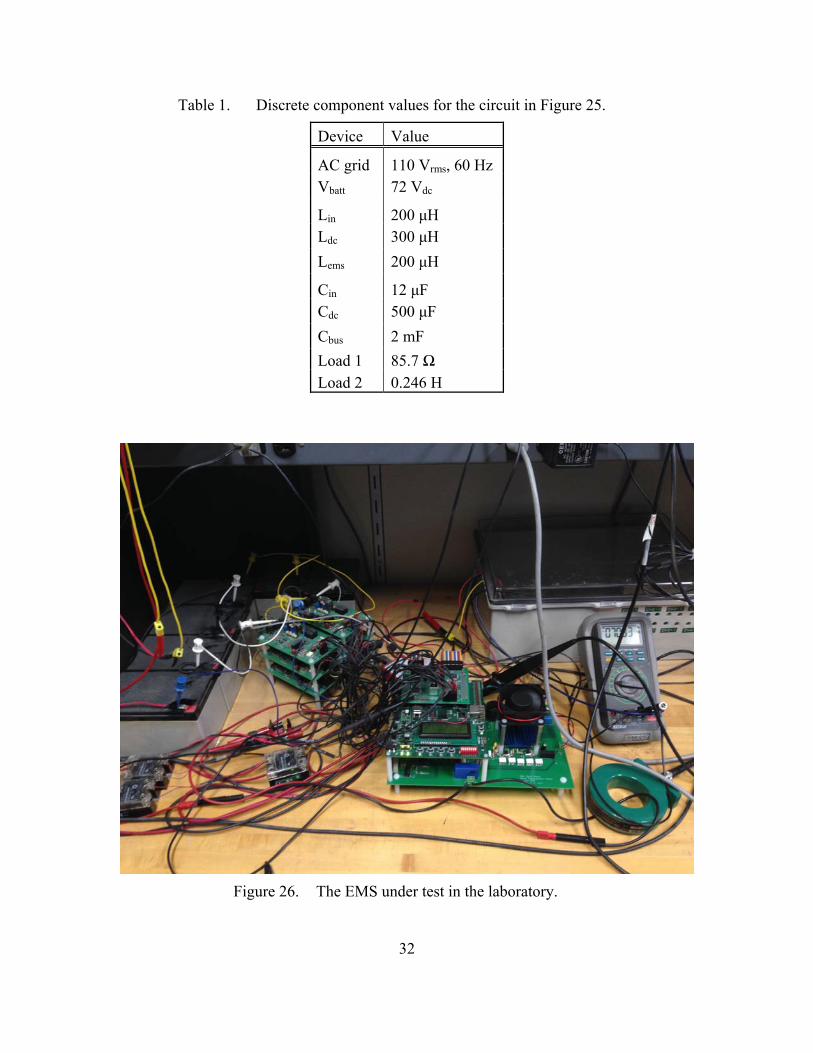
All discrete component values for the circuit in Figure 25 are given in Table 1.
Also, a digital photograph of the EMS under test is shown in Figure 26.
+
- vac
vdc
iems
+
vbatt-
+
-
Critical loads
Noncritical loads
ACgrid
Controller
Buckswitch
Boostswitch
H-bridge
iload
idc
isource
EMS
Cin
Lin
Lin
Cbus
Cdc
Ldc
Lems
Lems
Experimental EMS power electronics circuit schematic. Figure 25.
32
Table 1. Discrete component values for the circuit in Figure 25.
Device Value
AC grid 110 Vrms, 60 Hz Vbatt 72 Vdc
Lin 200 μH Ldc 300 μH
Lems 200 μH
Cin 12 μF Cdc 500 μF
Cbus 2 mF
Load 1 85.7 Ω Load 2 0.246 H
The EMS under test in the laboratory. Figure 26.

33
The oscilloscope, PC with Simulink and Xilinx software, and variable circuit
loads are not shown in Figure 26; however, the variable load panels are shown in the
photographs in Figure 27. The circuit loads were controlled by two load panels that
connected to the EMS. Each panel consists of three parallel sets of three parallel resistors
(300 Ω, 600 Ω, and 1200 Ω) or inductors (0.8 H, 1.6 H, and 3.2 H) to support up to three-
phase load applications. The variable load boxes were accordingly configured to facilitate
the experiment. This setup can be seen in Figure 27 where the appropriate resistor and
inductor switches were activated to provide the 85.7 Ω and 0.246 H parallel loads used in
the experiment.
Variable load panels used in the experiment. Figure 27.

34
B. PROCEDURE
Implementation of the experiment was a straightforward process. Upon
completing the lab setup, the Simulink simulation was compiled into VHDL code on a
PC and uploaded to the FPGA development board on the EMS using Xilinx software.
The VHDL code enabled the EMS to execute the power factor correction methodology
developed in Simulink.
The purpose of the experiment was to validate simulation results for the
compensation of an inductive power demand on the grid. Thus, both the 85.7 Ω resistive
load and 0.246 H inductive load were effective at the start of the experiment in order to
emulate circuit conditions similar to those modeled with Simulink upon activation of the
inductive load at 0.25 s into the simulation.
EMS functionality permitted the manual activation and deactivation of emsi ;
therefore, emsi was not immediately turned on so that the effects of the inductive power
demand on the grid could be observed and recorded using the oscilloscope. Once initial
measurements were collected, emsi was activated, and the resultant waveforms were
captured. The resultant experimental data is presented in Figures 28–31.
Since the EMS did not possess a current sensor at the source as previously
mentioned, the microcontroller was incapable of measuring sourcei and, therefore, could
not conduct closed-loop control of reference current *emsi . The EMS could only generate a
single emsi signal from the H-bridge inverter. Consequently, the EMS was merely able to
produce the 1.0 Apk continuous quadrature current waveform shown in Figure 13 to
compensate for a reactive power demand on the grid. Adjustments to *emsI based on
changes to sourcei were not possible with the current hardware configuration. However,
the purpose of the experiment was to demonstrate the potential of the EMS to compensate
for a reactive power demand on the source using the method tested in simulation. This
capability is confirmed by the experimental results.

35
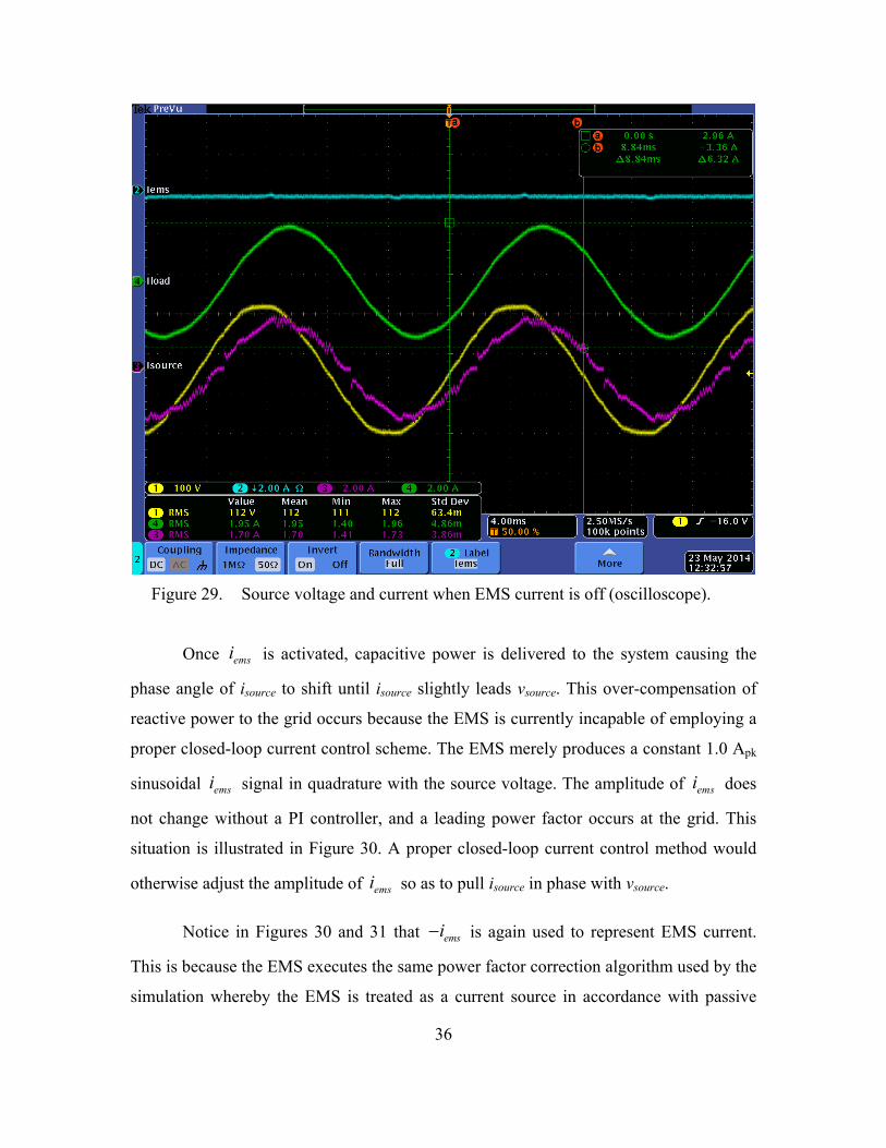
C. RESULTS
The ohmic-inductive circuit load initally creates an overall inductive reactance in
the circuit that results in a lagging power factor at the grid as expected. This is shown by
the source voltage and current waveforms in Figure 28 where isource lags vsource by
approximately 30⁰, which translates into an 87% source power factor. This power factor
is slightly improved over the 75% power factor initially realized in simulation; however,
this discrepancy is expected since the simulation does not account for the many electronic
devices that induce reactance throughout the EMS circuitry.
Notice also in Figure 28 that no reactive power compensation occurs since emsi is
not yet activated. There also appears to be small negative DC voltage component in the
source voltage of about −0.34 V. This DC offset is a consequence of calibration error in
the EMS voltage sensor since the equipment was not properly calibrated before the
experiment was conducted. Also of note, the voltage and current waveforms shown in
Figure 28 were created in MATLAB using data imported from the oscilloscope. The
oscilloscope display of the very same waveforms is provided for reference in Figure 29.
Source voltage and current when EMS current is off (MATLAB). Figure 28.
-0.02 -0.015 -0.01 -0.005 0 0.005 0.01 0.015 0.02-4
-3
-2
-1
0
1
2
3
4
Time (s)
Am
plit
ude
vsource
/50 (V)
isource
(A)
- iems
(A)
36
Source voltage and current when EMS current is off (oscilloscope). Figure 29.
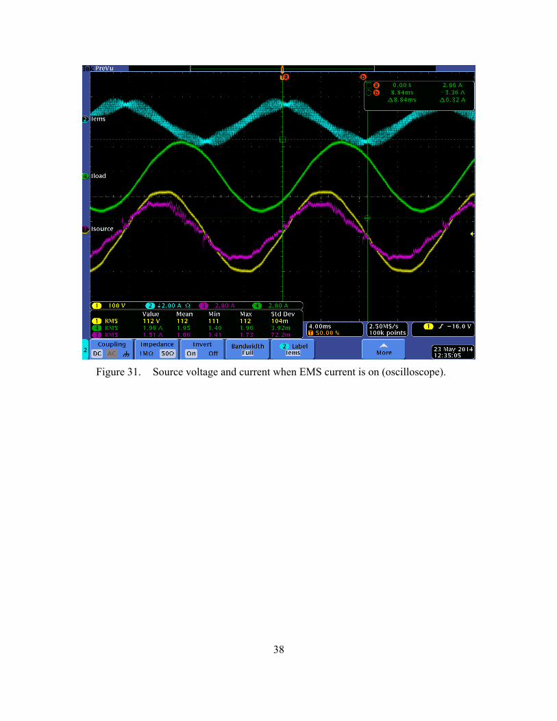
Once emsi is activated, capacitive power is delivered to the system causing the
phase angle of isource to shift until isource slightly leads vsource. This over-compensation of
reactive power to the grid occurs because the EMS is currently incapable of employing a
proper closed-loop current control scheme. The EMS merely produces a constant 1.0 Apk
sinusoidal emsi signal in quadrature with the source voltage. The amplitude of emsi does
not change without a PI controller, and a leading power factor occurs at the grid. This
situation is illustrated in Figure 30. A proper closed-loop current control method would
otherwise adjust the amplitude of emsi so as to pull isource in phase with vsource.
Notice in Figures 30 and 31 that emsi is again used to represent EMS current.
This is because the EMS executes the same power factor correction algorithm used by the
simulation whereby the EMS is treated as a current source in accordance with passive
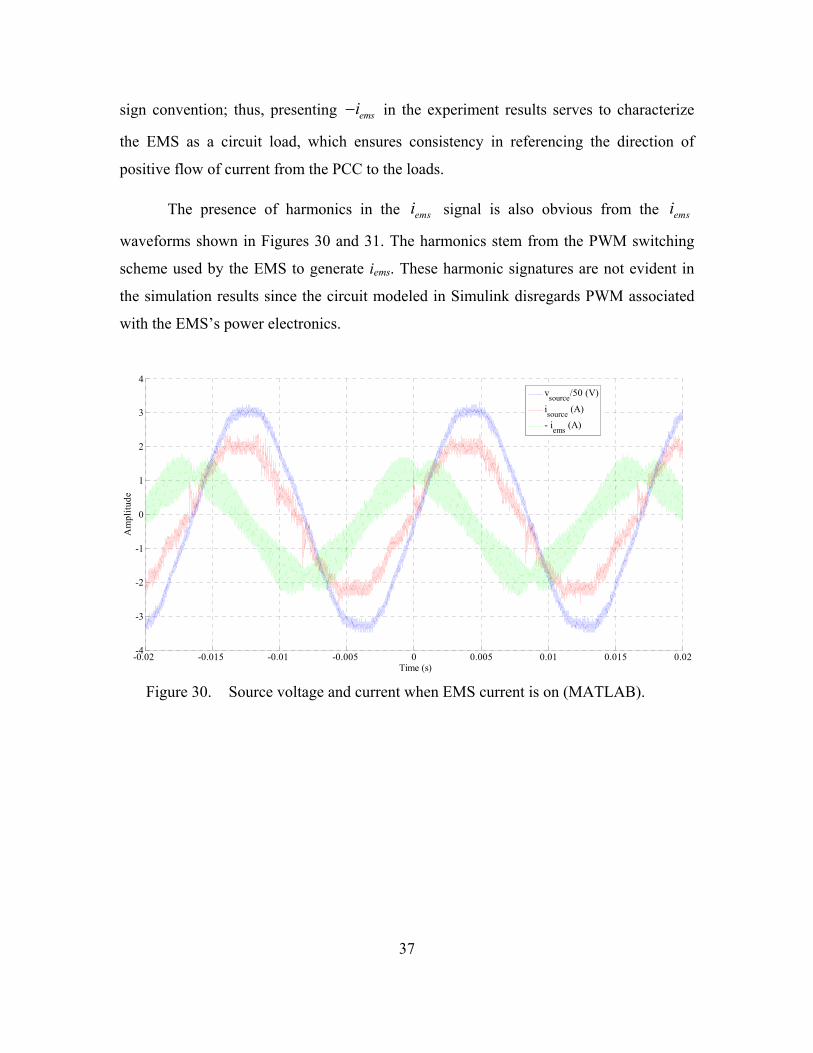
37
sign convention; thus, presenting emsi in the experiment results serves to characterize
the EMS as a circuit load, which ensures consistency in referencing the direction of
positive flow of current from the PCC to the loads.
The presence of harmonics in the emsi signal is also obvious from the emsi
waveforms shown in Figures 30 and 31. The harmonics stem from the PWM switching
scheme used by the EMS to generate iems. These harmonic signatures are not evident in
the simulation results since the circuit modeled in Simulink disregards PWM associated
with the EMS’s power electronics.
Source voltage and current when EMS current is on (MATLAB). Figure 30.
-0.02 -0.015 -0.01 -0.005 0 0.005 0.01 0.015 0.02-4
-3
-2
-1
0
1
2
3
4
Time (s)
Am
plit
ude
vsource
/50 (V)
isource
(A)
- iems
(A)
38
Source voltage and current when EMS current is on (oscilloscope). Figure 31.

39
V. CONCLUSIONS AND RECOMMENDATIONS
A. CONCLUSIONS
Reactive power compensation and power factor improvement are not new
engineering concepts. Controlling the generation, transmission, and distribution of
reactive energy in delivering quality power to the consumer is essential to increasing
energy efficiency and reducing energy costs. As a result, various methods for achieving a
unity power factor at the source have been developed and improved over time.
A particular means of compensating for a reactive power demand on the grid was
examined in this thesis whereby an additional capability to a particular EMS was
proposed that enabled the EMS to operate as current source in compensating for a
reactive power demand on the grid. This was accomplished by first using a Simulink-
based zero-crossing detection algorithm to determine the power factor angle between the
source voltage and current. The appropriate amount of reactive current was subsequently
injected into the system and adjusted using a closed-loop current control scheme that
brought the source current in phase with the source voltage thereby eliminating any
reactive power demand on the grid. A Simulink model of the process was initially
developed in order to forecast the system’s response to both capacitive and inductive
power demands on the grid. The process was then confirmed in a laboratory using the
actual EMS.
It is important to remember that the Simulink model was simplified so as to
isolate the reactive power compensation process for analysis by specifically neglecting to
model the EMS’s power electronics systems. The PWM scheme and related PI control of
the H-bridge IGBT gate signals in particular were disregarded. The EMS was thus
modeled as a constant current source. This eased the complexity of the simulation design
but created disparities between model functionality and actual EMS operation, which
caused some dissimilarity between simulation and experimental results.
For example, no harmonics were observed in the simulation representation of emsi
since the effects of the EMS’s power electronics were disregarded by the circuit modeled

40
in Simulink. Likewise, additional circuit reactance associated with discrete electronic
components was not observed in the simulation and, therefore, did not affect the reactive
power demand on the grid. Nevertheless, the results verified the ability of the EMS to
apply the Simulink-based power factor correction algorithm in compensating for a
reactive power demand on the grid.
Moreover, the EMS hardware did not possess a current sensor at the source, so
no closed-loop control of emsi was implemented in the laboratory. The EMS was
consequently unable to adjust the amplitude of emsi in correcting the source power factor
angle. The EMS still demonstrated the ability to improve the power factor at the source,
but a unity power factor could not be achieved without the use of closed-loop current
control. An EMS hardware upgrade is currently planned that will improve the
functionality of the EMS.
B. RECOMMENDATIONS
The results presented in this thesis built confidence in the ability of the EMS to
compensate for a reactive power demand on the grid; however, improving the simulation
and experiment could potentially facilitate a better understanding of the EMS’s
capabilities. It would be advantageous, for example, to repeat the experiment once a
source current sensor is installed in the EMS in order to fully validate the reactive power
compensation process designed in Simulink. Also, the simulation could be further
developed to simulate the EMS’s power electronics architecture, which includes the
PWM and controller required to operate the H-bridge inverter. Combining the two
aforementioned efforts into a single project might enable a better comparison of the
simulation and experiment results.
Additionally, future research into other reactive power compensation methods
involving the EMS would add depth to its functionality and facilitate a comparative
analysis of the different methods. Investigating the system’s response to various reactive
power demand scenarios might also assist in identifying the advantages and limitations of
each method. These results could then be used to develop a decision-making algorithm

41
that enables the EMS to choose an optimal power factor improvement process when
faced with varying power supply and demand situations.
One example of a potential alternative to the reactive power compensation
method presented in this thesis is the use of a phase-locked loop (PLL) control scheme to
detect and match the source current and voltage phase angles. While developing a PLL
control scheme may be a more complex design effort, it could potentially alleviate the
numerical integration error associated with zero-crossing detection when signal transients
are present in the source current.

42
THIS PAGE INTENTIONALLY LEFT BLANK

43
APPENDIX. MATLAB M-FILES
A. SIMULATION INITIAL CONDITIONS FILE
% Michael Prato % Reactive Power Compensation Using an EMS % Initial Conditions File clear all; clc; close all; V_source=120*sqrt(2); % Source voltage (V peak) freq=2*pi*60; % Source voltage frequency (rad) Kp=2/4; % Proportional gain of the PI controller Ki=100/4; % Integral gain of the PI controller R_load=85.714; % Resistive load (ohms) L_load=0.246; % Inductive load (H) R_of_L_load=5; % Resistance of the inductor (ohms) Rin=0.01; % Internal resistance (ohms) L_fil=400e-6; % Filter inductor (H) C_fil=12e-6; % Filter capacitor (F) tstep = 0.5e-5; % Step size (sec) tstop = 0.6; % Sim length (sec)
B. SIMULATION OUTPUT PLOT FILE
% Michael Prato % Reactive Power Compensation Using an EMS % Output Plot File % Replicates oscilloscope waveforms based on output data files collected from the oscilloscope v_cap=data_out(:,1); i_source=data_out(:,2); i_ems=data_out(:,3); i_load=data_out(:,4); filtered_PF_angle=data_out(:,5); v_source=data_out(:,6); i_ems_amplitude=data_out(:,7); i_phase_angle=data_out(:,8); v_phase_angle=data_out(:,9); calculated_PF_angle=data_out(:,10); corrected_PF_angle=data_out(:,11); figure(‘name’,’Reactive Power Compensation’); hold on; plot(time,v_source/50,’b’,’linewidth’,1.5); plot(time,i_source,’r’,’linewidth’,1.5) plot(time,-i_ems,’g’,’linewidth’,1.5) xlabel(‘Time (s)’,’FontSize’,20); ylabel(‘Amplitude’,’FontSize’,20); xlim([0 tstop]); legend(‘v_s_o_u_r_c_e/50 (V)’,’i_s_o_u_r_c_e (A)’,’- i_e_m_s (A)’);

44
grid on; hold off; figure(‘name’,’Grid Power Factor’); plot(time,cos(calculated_PF_angle),’linewidth’,2); xlabel(‘Time (s)’,’FontSize’,20); ylabel(‘Grid Power Factor’,’FontSize’,20); xlim([0 tstop]); ylim([0.75 1.02]); grid on; figure(‘name’,’Reactive Power Compensation by Achieving a Unity PF, Ohmic Load’); subplot(2,1,1); grid on; hold on; plot(time,v_source/50,’b’,’linewidth’,2); plot(time,i_source,’r’,’linewidth’,2) plot(time,-i_ems,’g’,’linewidth’,2) %title(‘Purely Resistive Load (85.7 \Omega)’,’FontSize’,20); xlim([0 0.25]); xlabel(‘Time (s)’,’FontSize’,20); ylabel(‘Amplitude’,’FontSize’,20); legend(‘v_s_o_u_r_c_e/50 (V)’,’i_s_o_u_r_c_e (A)’,’- i_e_m_s (A)’,’location’,’south’); subplot(2,1,2); plot(time,cos(calculated_PF_angle),’linewidth’,2); grid on; xlabel(‘Time (s)’,’FontSize’,20); ylabel(‘Grid Power Factor’,’FontSize’,20); %title(‘Power Factor’,’FontSize’,20); xlim([0 0.25]); ylim([0.93 1.005]); figure(‘name’,’Reactive Power Compensation by Achieving a Unity PF, Inductive Load’); subplot(2,1,1); grid on; hold on; plot(time,v_source/50,’b’,’linewidth’,2); plot(time,i_source,’r’,’linewidth’,2) plot(time,-i_ems,’g’,’linewidth’,2) %title(‘Inductive Load (0.246 H) Added to the Circuit at t = 0.25 s’,’FontSize’,20); xlabel(‘Time (s)’,’FontSize’,20); ylabel(‘Amplitude’,’FontSize’,20); xlim([0.25 tstop]); legend(‘v_s_o_u_r_c_e/50 (V)’,’i_s_o_u_r_c_e (A)’,’- i_e_m_s (A)’,’location’,’south’); subplot(2,1,2); plot(time,cos(calculated_PF_angle),’linewidth’,2); grid on; xlabel(‘Time (s)’,’FontSize’,20); ylabel(‘Grid Power Factor’,’FontSize’,20); %title(‘Power Factor’,’FontSize’,20); xlim([0.25 tstop]); ylim([0.75 1.02]); figure(‘name’,’Phase Angles’) plot(time,v_phase_angle*180/pi,’b’,’linewidth’,1.5); hold on; plot(time,i_phase_angle*180/pi,’g’,’linewidth’,1.5); hold off;

45
xlabel(‘Time (s)’,’FontSize’,16); ylabel(‘Phase Angle, \theta (deg)’,’FontSize’,16); legend(‘\theta_v__s_o_u_r_c_e’,’\theta_i__s_o_u_r_c_e’,’FontSize’,16); xlim([0 tstop]); ylim([0 410]); grid on; figure(‘name’,’Phase Angles from t=[0,0.6]sec’) subplot(2,1,1); grid; hold on; plot(time,v_phase_angle*180/pi,’b’,’linewidth’,1.5); plot(time,i_phase_angle*180/pi,’g’,’linewidth’,1.5); hold off; title(‘Resistive Load (85.7 \Omega)’,’FontSize’,20); xlim([0 0.25]); xlabel(‘Time (s)’,’FontSize’,16); ylabel(‘Phase Angle, \theta (deg)’,’FontSize’,20); legend(‘\theta_v__s_o_u_r_c_e’,’\theta_i__s_o_u_r_c_e’); subplot(2,1,2); grid; hold on; plot(time,v_phase_angle*180/pi,’b’,’linewidth’,1.5); plot(time,i_phase_angle*180/pi,’g’,’linewidth’,1.5); hold off; title(‘Inductive Load (0.246 H) Added to the Circuit at t = 0.25 s’,’FontSize’,20); xlim([0.25 tstop]); xlabel(‘Time (s)’,’FontSize’,16); ylabel(‘Phase Angle, \theta (deg)’,’FontSize’,20); legend(‘\theta_v__s_o_u_r_c_e’,’\theta_i__s_o_u_r_c_e’); figure(‘name’,’Phase Angles from t=[0,0.35]sec’) subplot(2,1,1); grid; hold on; plot(time,v_phase_angle*180/pi,’b’,’linewidth’,2); plot(time,i_phase_angle*180/pi,’g’,’linewidth’,2); hold off; title(‘Resistive Load (85.7 \Omega)’,’FontSize’,20); xlim([0 0.1]); xlabel(‘Time (s)’,’FontSize’,20); ylabel(‘Phase Angle, \theta (deg)’,’FontSize’,20); legend(‘\theta_v__s_o_u_r_c_e’,’\theta_i__s_o_u_r_c_e’,’location’,’southeast’); subplot(2,1,2); grid; hold on; plot(time,v_phase_angle*180/pi,’b’,’linewidth’,2); plot(time,i_phase_angle*180/pi,’g’,’linewidth’,2); hold off; title(‘Inductive Load (0.246 H) Added to the Circuit at t = 0.25 sec’,’FontSize’,20); xlim([0.25 0.35]); xlabel(‘Time (s)’,’FontSize’,16); ylabel(‘Phase Angle, \theta (deg)’,’FontSize’,20); legend(‘\theta_v__s_o_u_r_c_e’,’\theta_i__s_o_u_r_c_e’);

46
figure(‘name’,’Calculated PF Angle Between Source Voltage and Source Current’) plot(time,calculated_PF_angle*180/pi,’b’,’linewidth’,2); xlabel(‘Time (s)’,’FontSize’,20); ylabel(‘Calculated PF Angle, \phi (deg)’,’FontSize’,20); grid on; xlim([0 tstop]); figure(‘name’,’Corrected and Filtered Power Factor Angle’) subplot(2,1,1),plot(time,corrected_PF_angle*180/pi,’b’,’linewidth’,2); grid; xlim([0 tstop]); xlabel(‘Time (s)’,’FontSize’,20); ylabel(‘Corrected PF Angle, \phi (deg)’,’FontSize’,20); %legend(‘Unfiltered \phi (\theta_v__s_o_u_r_c_e - \theta_i__s_o_u_r_c_e)’,’location’,’south’); subplot(2,1,2),plot(time,filtered_PF_angle*180/pi,’b’,’linewidth’,2); grid; xlim([0 tstop]); xlabel(‘Time (s)’,’FontSize’,20); ylabel(‘Filtered PF Angle, \phi (deg)’,’FontSize’,20); %legend(‘Filtered \phi (\theta_v__s_o_u_r_c_e - \theta_i__s_o_u_r_c_e)’,’location’,’south’); grid on; figure(‘name’,’Power Factor Angle and EMS Current Amplitude’) subplot(2,1,1),plot(time,filtered_PF_angle*180/pi,’b’,’linewidth’,2); grid; xlim([0 tstop]); xlabel(‘Time (s)’,’FontSize’,20); ylabel(‘Filtered PF Angle, \phi (deg)’,’FontSize’,20); %legend(‘Filtered \phi (\theta_v__s_o_u_r_c_e - \theta_i__s_o_u_r_c_e)’,’location’,’south’); subplot(2,1,2),plot(time,i_ems_amplitude,’g’,’linewidth’,2); grid; xlim([0 tstop]); xlabel(‘Time (s)’,’FontSize’,20); ylabel(‘EMS Current Amplitude, I^*_e_m_s (A)’,’FontSize’,20); grid on;
C. EXPERIMENT OUTPUT PLOT FILE
% Michael Prato % Reactive Power Compensation Using an EMS % Oscilloscope Output Plot File Clc; clear all; close all; data_vac=xlsread(‘Tek_CH1_Wfm.csv’); data_iems=xlsread(‘Tek_CH2_Wfm.csv’); data_isource=xlsread(‘Tek_CH3_Wfm.csv’); data_iload =xlsread(‘Tek_CH4_Wfm.csv’); len = length(data_vac); time_vec=data_vac(15:len,1); vac=data_vac(15:len,2); iems=data_iems(15:len,2);

47
iload=data_iload(15:len,2); isource=data_isource(15:len,2); tmin=time_vec(1); tmax=max(time_vec); data_vac2=xlsread(‘Tek_CH1_Wfmb.csv’); data_iems2=xlsread(‘Tek_CH2_Wfmb.csv’); data_isource2=xlsread(‘Tek_CH3_Wfmb.csv’); data_iload2 =xlsread(‘Tek_CH4_Wfmb.csv’); len = length(data_vac2); time_vec2=data_vac2(15:len,1); vac2=data_vac2(15:len,2); iems2=data_iems2(15:len,2); iload2=data_iload2(15:len,2); isource2=data_isource2(15:len,2); tmin2=time_vec(1); tmax2=max(time_vec); figure(1); subplot(2,1,1), plot(time_vec,vac/50); hold on; plot(time_vec,isource,’r’); hold off; xlabel(‘Time (s)’); ylabel(‘Amplitude’); legend(‘v_s_o_u_r_c_e/50 (V)’,’i_s_o_u_r_c_e (A)’,’Location’,’Northeast’); grid on; axis([tmin tmax -4 4]); subplot(2,1,2),plot(time_vec,iems,’g’,time_vec,iload,’m’); xlabel(‘Time (s)’); ylabel(‘Amplitude’); grid on; legend(‘-i_e_m_s (A)’,’i_l_o_a_d (A)’,’Location’,’Northeast’); axis([tmin tmax -4 4]); temp1=get(gcf,’position’); temp2=temp1+[-500, 0, temp1(3)*1.5, 0 ]; set(gcf,’position’,temp2); saveas(gcf,’figure1’,’tif’); print(gcf,’-dtiff’,’-r350’,’figure1’); figure(2); subplot(2,1,1), plot(time_vec2,vac2/50); hold on; plot(time_vec2,isource2,’r’); hold off; xlabel(‘Time (s)’); ylabel(‘Amplitude’); legend(‘v_s_o_u_r_c_e/50 (V)’,’i_s_o_u_r_c_e (A)’,’Location’,’Northeast’); grid on; axis([tmin tmax -4 4]);

48
subplot(2,1,2),plot(time_vec2,iems2,’g’,time_vec2,iload2,’m’); xlabel(‘Time (s)’); ylabel(‘Amplitude’); grid on; legend(‘-i_e_m_s (A)’,’i_l_o_a_d (A)’,’Location’,’Northeast’); axis([tmin tmax -4 4]); temp1=get(gcf,’position’); temp2=temp1+[-500, 0, temp1(3)*1.5, 0 ]; set(gcf,’position’,temp2); saveas(gcf,’figure2’,’tif’); print(gcf,’-dtiff’,’-r350’,’figure2’); figure(3); hold on; plot(time_vec2,vac/50); plot(time_vec2,isource,’r’); plot(time_vec2,iems,’g’); hold off; xlabel(‘Time (s)’); ylabel(‘Amplitude’); legend(‘v_s_o_u_r_c_e/50 (V)’,’i_s_o_u_r_c_e (A)’,’- i_e_m_s (A)’,’Location’,’Northeast’); grid on; axis([tmin tmax -4 4]); temp1=get(gcf,’position’); temp2=temp1+[-500, 0, temp1(3)*1.5, 0 ]; set(gcf,’position’,temp2); saveas(gcf,’figure3’,’tif’); print(gcf,’-dtiff’,’-r350’,’figure3’); figure(4); hold on; plot(time_vec2,vac2/50); plot(time_vec2,isource2,’r’); plot(time_vec2,iems2,’g’); hold off; xlabel(‘Time (s)’); ylabel(‘Amplitude’); legend(‘v_s_o_u_r_c_e/50 (V)’,’i_s_o_u_r_c_e (A)’,’- i_e_m_s (A)’,’Location’,’Northeast’); grid on; axis([tmin tmax -4 4]); temp1=get(gcf,’position’); temp2=temp1+[-500, 0, temp1(3)*1.5, 0 ]; set(gcf,’position’,temp2); saveas(gcf,’figure4’,’tif’); print(gcf,’-dtiff’,’-r350’,’figure4’); figure(5); hold on;

49
plot(time_vec,vac/50); plot(time_vec,isource,’r’); plot(time_vec,iems,’g’); plot(time_vec,iload,’m’); hold off; xlabel(‘Time (s)’); ylabel(‘Amplitude’); legend(‘v_s_o_u_r_c_e/50 (V)’,’i_s_o_u_r_c_e (A)’,’-i_e_m_s (A)’,’i_l_o_a_d (A)’,’Location’,’Northeast’); grid on; axis([tmin tmax -4 4]); temp1=get(gcf,’position’); temp2=temp1+[-500, 0, temp1(3)*1.5, 0 ]; set(gcf,’position’,temp2); saveas(gcf,’figure5’,’tif’); print(gcf,’-dtiff’,’-r350’,’figure3’); figure(6); hold on; plot(time_vec,vac2/50); plot(time_vec,isource2,’r’); plot(time_vec,iems2,’g’); plot(time_vec,iload2,’m’); hold off; xlabel(‘Time (s)’); ylabel(‘Amplitude’); legend(‘v_s_o_u_r_c_e/50 (V)’,’i_s_o_u_r_c_e (A)’,’-i_e_m_s (A)’,’i_l_o_a_d (A)’,’Location’,’Northeast’); grid on; axis([tmin tmax -4 4]); temp1=get(gcf,’position’); temp2=temp1+[-500, 0, temp1(3)*1.5, 0 ]; set(gcf,’position’,temp2); saveas(gcf,’figure6’,’tif’); print(gcf,’-dtiff’,’-r350’,’figure4’);

50
THIS PAGE INTENTIONALLY LEFT BLANK

51
LIST OF REFERENCES
[1] United States Marine Corps Expeditionary Energy Strategy and Implementation Plan, Washington, DC: Marine Corps Expeditionary Energy Office, 2011.
[2] W. Hofmann, and J. Schlabbach, W. Just, Reactive Power Compensation: A Practical Guide. Chichester, UK: John Wiley & Sons, Ltd., 2012.
[3] S. Booth, J. Barnett, K. Burman, J. Hambrick, and R. Westby, “Net zero energy military installations: A guide to assessment and planning,” National Renewable Energy Lab., Golden, CO, Tech. Rep. NREL/TP-7A2–48876, Aug. 2010.
[4] Commission Staff Report, “Payment for reactive power,” Federal Energy Regulatory Commission, Washington, DC, Rep. AD14–7, Apr. 22, 2014.
[5] Simulink® by MathWorks [Online]. http://www.mathworks.com/products/simulink
[6] R. L. Kelly, “Optimizing gas generator efficiency in a forward operating base using an energy management system,” M.S. thesis, Dept. Elect. Comp. Eng., Naval Postgraduate School, Monterey, CA, 2013.
[7] A. J. Metzcus, “H-bridge inverter loading analysis for an energy management system,” M.S. thesis, Dept. Elect. Comp. Eng., Naval Postgraduate School, Monterey, CA, 2013.
[8] N. J. Peck, “Peak power control with an energy management system,” M.S. thesis, Dept. Elect. Comp. Eng., Naval Postgraduate School, Monterey, CA, 2013.
[9] R. Carnieletto, D. I. Brandão, S. Suryanarayanan, F. A. Farret, and M. G. Simões, “Smart grid initiative,” IEEE Ind. Appl. Mag., vol. 17, no. 5, pp. 27–35, Sep./Oct. 2011.
[10] J. He, Y. W. Li, F. B. Blaabjerg, and X. Wang, “Active harmonic filtering using current-controlled, grid-connected DG units with closed-loop power control,” IEEE Trans. Power Electron., vol. 29, no. 2, pp. 642–653, Feb. 2014.
[11] G. Oriti, A. L. Julian, and N. J. Peck, “Power electronics enabled energy management systems,” in Proceedings of IEEE Applied Power Electronics Conference, Long Beach, CA, Mar. 2013, pp. 3224–3231.
[12] Xilinx® system generator for DSP: Getting started guide (v14.3) [Online]. Available: http://www.xilinx.com/support/
[13] N. Mohan, T. M. Undeland, and W. P. Robbins, Power Electronics: Converters, Applications, and Design, 3rd ed. New York: John Wiley & Sons, Inc., 2003.

52
THIS PAGE INTENTIONALLY LEFT BLANK

53
INITIAL DISTRIBUTION LIST
1. Defense Technical Information Center Ft. Belvoir, Virginia 2. Dudley Knox Library Naval Postgraduate School Monterey, California