rdug le51hr0128
TRANSCRIPT

User Guide
Part Number: Le51HR0128
Revision Number: 3.0
Issue Date: March 2016
Document Number: 127669
Le51HR0128NGCC Configuration C
8-Channel POTS Line Module
CONFIDENTIAL

Le51HR0128 Design Manual
2
Microsemi Corporation Confidential and Proprietary
1.0 Introduction . . . . . . . . . . . . . . . . . . . . . . . . . . . . . . . . . . . . . . . . . . . . . . . . . . . . . . . . . . . . . . . . . . . . . . . . . . . 31.1 Overview . . . . . . . . . . . . . . . . . . . . . . . . . . . . . . . . . . . . . . . . . . . . . . . . . . . . . . . . . . . . . . . . . . . . . . . . . . . 31.2 Design Objectives . . . . . . . . . . . . . . . . . . . . . . . . . . . . . . . . . . . . . . . . . . . . . . . . . . . . . . . . . . . . . . . . . . . . 31.3 Disclaimer . . . . . . . . . . . . . . . . . . . . . . . . . . . . . . . . . . . . . . . . . . . . . . . . . . . . . . . . . . . . . . . . . . . . . . . . . . 41.4 Reference documents . . . . . . . . . . . . . . . . . . . . . . . . . . . . . . . . . . . . . . . . . . . . . . . . . . . . . . . . . . . . . . . . . 4
2.0 Quick Start Guide. . . . . . . . . . . . . . . . . . . . . . . . . . . . . . . . . . . . . . . . . . . . . . . . . . . . . . . . . . . . . . . . . . . . . . . 52.1 Important Power Consideration . . . . . . . . . . . . . . . . . . . . . . . . . . . . . . . . . . . . . . . . . . . . . . . . . . . . . . . . . . 52.2 Set-Up Procedure . . . . . . . . . . . . . . . . . . . . . . . . . . . . . . . . . . . . . . . . . . . . . . . . . . . . . . . . . . . . . . . . . . . . 5
3.0 System Description . . . . . . . . . . . . . . . . . . . . . . . . . . . . . . . . . . . . . . . . . . . . . . . . . . . . . . . . . . . . . . . . . . . . . 73.1 Features . . . . . . . . . . . . . . . . . . . . . . . . . . . . . . . . . . . . . . . . . . . . . . . . . . . . . . . . . . . . . . . . . . . . . . . . . . . 73.2 System Features . . . . . . . . . . . . . . . . . . . . . . . . . . . . . . . . . . . . . . . . . . . . . . . . . . . . . . . . . . . . . . . . . . . . . 8
3.2.1 NGSLIC Features. . . . . . . . . . . . . . . . . . . . . . . . . . . . . . . . . . . . . . . . . . . . . . . . . . . . . . . . . . . . . . . . 83.2.2 NGSLAC Features . . . . . . . . . . . . . . . . . . . . . . . . . . . . . . . . . . . . . . . . . . . . . . . . . . . . . . . . . . . . . . . 83.2.3 NGVCP Features . . . . . . . . . . . . . . . . . . . . . . . . . . . . . . . . . . . . . . . . . . . . . . . . . . . . . . . . . . . . . . . . 9
3.3 ID EEPROM . . . . . . . . . . . . . . . . . . . . . . . . . . . . . . . . . . . . . . . . . . . . . . . . . . . . . . . . . . . . . . . . . . . . . . . . 9
4.0 Circuit Design. . . . . . . . . . . . . . . . . . . . . . . . . . . . . . . . . . . . . . . . . . . . . . . . . . . . . . . . . . . . . . . . . . . . . . . . . 104.1 Transmission and Loop Feed . . . . . . . . . . . . . . . . . . . . . . . . . . . . . . . . . . . . . . . . . . . . . . . . . . . . . . . . . . 104.2 Ringing . . . . . . . . . . . . . . . . . . . . . . . . . . . . . . . . . . . . . . . . . . . . . . . . . . . . . . . . . . . . . . . . . . . . . . . . . . . 104.3 Test Capability. . . . . . . . . . . . . . . . . . . . . . . . . . . . . . . . . . . . . . . . . . . . . . . . . . . . . . . . . . . . . . . . . . . . . . 104.4 Protection . . . . . . . . . . . . . . . . . . . . . . . . . . . . . . . . . . . . . . . . . . . . . . . . . . . . . . . . . . . . . . . . . . . . . . . . . 104.5 Metering. . . . . . . . . . . . . . . . . . . . . . . . . . . . . . . . . . . . . . . . . . . . . . . . . . . . . . . . . . . . . . . . . . . . . . . . . . . 104.6 Board Power . . . . . . . . . . . . . . . . . . . . . . . . . . . . . . . . . . . . . . . . . . . . . . . . . . . . . . . . . . . . . . . . . . . . . . . 104.7 HBI Control . . . . . . . . . . . . . . . . . . . . . . . . . . . . . . . . . . . . . . . . . . . . . . . . . . . . . . . . . . . . . . . . . . . . . . . . 114.8 Signal Integrity when Using Multiple Line Modules . . . . . . . . . . . . . . . . . . . . . . . . . . . . . . . . . . . . . . . . . . 11
5.0 Evaluation Tools . . . . . . . . . . . . . . . . . . . . . . . . . . . . . . . . . . . . . . . . . . . . . . . . . . . . . . . . . . . . . . . . . . . . . . 12
6.0 Schematics and Bill of Materials . . . . . . . . . . . . . . . . . . . . . . . . . . . . . . . . . . . . . . . . . . . . . . . . . . . . . . . . . 13
CONFIDENTIAL

Le51HR0128 User Guide
1.0 Introduction
1.1 Overview
The Le51HR0128 line module provides a compact, eight-channel balanced internal ringing solution for POTSapplications. The line module is comprised of an octal Le792388 Next Generation SLAC device and eight Le79271Next Generation SLIC devices with loop protection. Meter pulse is supported.
The line module is controlled by the Microsemi Telephony Applications Platform (ZTAP) and is directly plugged intothe Microsemi Backplane (ZBP) 9 or ZBP2 motherboard which provides power to the line module and ZBP via anexternal power cable.
The ZBP motherboard brings versatility to the line module. The motherboard has slots for POTS splitter cardswhich can be used with the line module for IVD applications. The motherboard also provides the additionalfunctionality of the Le79124 Next Generation Voice Control Processor (NGVCP) device. The NGVCP deviceprovides control for up to nine Le51HR0128 line modules (72 channels). It also provides Advanced Test capabilityto all of the channels.
The Le51HR0128 line module is RoHS Directive 2002/95/EC compliant.
Figure 1 - Le51HR0128 Line Module - Top View
1.2 Design Objectives
The Le51HR0128 line module design objectives:
• Provide 8-channel of POTS
• Support Microsemi Configuration C no calibration architecture. See Figure 2.
• Support PPM transmission
• Provide secondary protection (as a reference)CONFIDENTIAL
3
Microsemi Corporation Confidential and Proprietary

Le51HR0128 User Guide
Figure 2 - Microsemi Configuration C Architecture
1.3 Disclaimer
This circuit design is provided as reference only, without warranty expressed or implied. The user is encouraged toperform all due diligence with respect to design and analysis.
1.4 Reference documents
The following documents may be helpful in understanding operation of this line module:
1. VoicePathTM Profile Wizard User’s Guide, Document ID #LE71SDKPRO.
2. Universal VoicePath Demo Platform - Getting Started Guide, Document ID #081310.
3. Mini-PBX User’s Guide, Document ID #081355.
4. Le51HR0134 Microsemi Back Plane 9 User Guide, Document ID #125881.
5. Le51HR0136 Microsemi Back Plane 2 User Guide, Document ID #126961.
6. Le79124-SW Next Generation VoiceEdgeTM Control Processor Software Package Data Sheet, Document ID #127671.
7. Le79124 Next Generation VoiceEdgeTM Control Processor Data Sheet, Document ID #081567.
8. Le79238 Next Generation Octal SLAC Device Data Sheet, Document ID #081193
9. Le79271 Next Generation SLIC Device Data Sheet, Document ID #081555
10.NGCC Hardware Design Guide, Document ID #126583.
B (RING)
A (TIP)AD
BD
NGSLAC SVA
Le79271NGSLIC
Over-VoltageProtection
AD
BD
VBP
VBH
TLD
PTC orResistor
PTC orResistor
RLOAD
(optional)
NGSLAC SVB
CONFIDENTIAL
4
Microsemi Corporation Confidential and Proprietary

Le51HR0128 User Guide
2.0 Quick Start Guide
2.1 Important Power Consideration
All power must be turned off before inserting the line module. Turn off power supplies before removing theline module.
2.2 Set-Up Procedure
The Le51HR0128 line module mates to the ZBP motherboard which is plugged into the ZTAP horizontal DINconnector. This quick start guide assumes power comes from user supplied power supplies connected to the ZBPExternal Power Connector.
Quick start steps for 1 line module:
1. Plug the ZBP motherboard into the ZTAP DIN connector. Remove any power supply jumpers on the ZBP moth-erboard. The jumpers are located next to the DIN connector and are labeled +3.3V1, +5V1, +12V1, VBATP1, VBATL1, and VBATH1.
2. Set DIP Switch on ZBP motherboard for 00100010 for NGVCP use or 00100001 for no NGVCP use. A “0” state is when the switch is in the ON (down) position. Refer to the appropriate ZPB User Guide for more information.
3. Plug the Le51HR0128 line module into connector slot 1.
4. If a POTS splitter is to be used, plug IVD splitter modules into the 36-pin IVD slots.
5. The Le51HR0128 line module requires +3.3 V, +1.8 V, VBL, VBH and VBP power supplies.
The +3.3 V supply will power the entire ZBP motherboard as well as the individual line modules, select a supplycapable of driving at least 2 amps (5 amps if using ZBP9 and multiple line modules). The ZBP motherboardprovides a +3.3 V to +1.8 V converter for line module use.
The dc feed coefficients programmed into the line module IDROM assumes a VBL of -35 V and a VBH of -59 V.The current requirement for these high voltage supplies is dependent upon the intended number of off-hookloads. Select a supply capable of providing at least 50 mA times the number of off-hook channels. The ringingcoefficients programmed into the line module IDROM assumes a VBP value of +59 V. Set all the supplies to thedesired voltages and then power them down.
Connect a Microsemi external power cable (OPN Le51HW0109) to the External Power Connector. Connect allthe ground leads together and wire to the +3.3 V supply negative terminal and ground. Jumper this ground nodeto the appropriate terminals on all the battery supplies. Wire the lead labeled +3.3 V to the low voltage supply.Wire the VBL and VBH leads to the negative high voltage supplies. (If using only one negative battery, tie bothVBL and VBH leads to the negative output). Wire VBP to the positive high voltage supply.
6. Plug the Power Brick into the ZTAP power connector (J6101) and turn on the adjacent switch. Also turn on the +3.3 V and all the VPx external power supplies.
7. Using Toolkit, Open Vp-Script using the following settings:
• Platform: Select ZTAP as appropriate
• Port: Select appropriate Com port
• Select Add/Exit
VP-Script will open.
8. Next from Toolkit, open Mini-PBX. The Mini-PBX window will appear. After a delay, the Call Control Restart Detection dialog box appears. Click Yes. Mini-PBX will read the Le51HR0128 IDROM and set-up 8 extensions CONFID
ENTIAL
5
Microsemi Corporation Confidential and Proprietary

Le51HR0128 User Guide
of FXS. That is, an FXS_Generic Line Termination Type (Microsemi configuration C) connection. A set of DC, AC, and ring profiles will be loaded into the chip set.
Note: In Mini-PBX select Configuration Mode, then right click on DIN CS0 in the Device window Delete Selected Device. Right click again in the Device window Add New Device. Set up the device using these entries DIN, CS0, SPI8, 792_SERIES, FXS, 8, 100. Finally implement changes by selecting Load Override File (to Host) followed by Run Config File.
9. Telephone calls can now be set up between extensions by dialing the appropriate 4 digit extension number (x7100 - x7107). The NGSLAC will recognize DTMF or dial pulse digits.
Line testing can also be performed if NGVCP use was selected via the DIP Switch setting. Double click on the extension number of the channel to be tested and then select the Line Testing tab followed by the appropriate Line Test Package and Test.
To use external test equipment, TX and RX signals from a PCM Channel Measuring Set must be wired to the E1/T1 port on the T1/E1 ports on the ZTAP. From Mini-PBX Options menu, E1 or T1 PCM Framing must be selected (even if selection is already checked). Double click on the extension number of the channel to be tested and then select the Half Channel test tab. Select Talk state to disable the call progress tones. Analog connections to tip/ring can now be made and the line can be tested.
CONFIDENTIAL
6
Microsemi Corporation Confidential and Proprietary

Le51HR0128 User Guide
3.0 System Description
3.1 Features
The Le51HR0128 line module features one octal Le792388 NGSLAC device and eight Le79271 NGSLIC devices.The ZBP motherboard features an FPGA, an Le79124 NGVCP device, and optional IVD splitters (not shown).
Figure 3 - System Block Diagram
INTn GPIO
GPIO
MPIMPI
ZTA
P Platform
Le792388
NGSLAC
A3 (Tip)
B3 (Ring) PTC
PTC
A4 (Tip)
B4 (Ring) PTC
PTC
Prot
Prot
A5 (Tip)
B5 (Ring) PTC
PTC
A6 (Tip)
B6 (Ring) PTC
PTC
Prot
Prot
A7 (Tip)
B7 (Ring) PTC
PTC
A8 (Tip)
B8 (Ring) PTC
PTC
Prot
Prot
A1 (Tip)
B1 (Ring) PTC
PTC
A2 (Tip)
B2 (Ring) PTC
PTC
Prot
Prot CSn
PCMPCM
FPGA
Le79124NGVCP
Control
MPI
PCM
ZBP M
otherbo
ard
RCVP RCVP1
IMT VAC1
AD
BD
TLD
Le79271NGSLIC
RCVN1RCVN
RCVP RCVP2
IMT VAC2
AD
BD
TLDRCVN2RCVN
RCVP RCVP3
IMT VAC3
AD
BD
TLDRCVN3RCVN
RCVP RCVP4
IMT VAC4
AD
BD
TLDRCVN4RCVN
RCVP RCVP5
IMT VAC5
AD
BD
TLD
Le79271NGSLIC
RCVN5RCVN
RCVP RCVP6
IMT VAC6
AD
BD
TLD
Le79271NGSLIC
RCVN6RCVN
RCVP RCVP7
IMT VAC7
AD
BD
TLD
Le79271NGSLIC
RCVN7RCVN
RCVP RCVP8
IMT VAC8
AD
BD
TLD
Le79271NGSLIC
RCVN8RCVN
P-bus
P-bus
P-bus
P-bus
P-bus
P-bus
P-bus
P-bus
Le79271NGSLIC
Le79271NGSLIC
Le79271NGSLIC
Le51
HR0128
Line M
odule
CONFIDENTIAL
7
Microsemi Corporation Confidential and Proprietary

Le51HR0128 User Guide
3.2 System Features
The Le51HR0128 line module features the following:
• NGCC highly integrated and programmable chip set
• PTC and battery referenced NGSLIC surge protection is provided on the line module in order to offer a complete reference design. Note, the ZBP platform is not designed to be subjected to lightning or power cross surges.
The ZBP motherboard features the following:
• Le79124 NGVCP with Advanced Test Plus capability and control of nine line modules
• FPGA for configuration options and signal buffering
• Slots for IVD splitters
• RJ11 plugs for connection to tip/ring
3.2.1 NGSLIC Features
• Voice transmission
• Internal ringing up to 85 Vrms
• Power saving auto-battery operation
• Per-channel test load (TLD)
3.2.2 NGSLAC Features
• Gain blocks, companding, 2-wire AC impedance, transhybrid balance, equalization
• NGSLIC control through P-bus interface
• DC loop feeding
• Supervision
• Internal ringing generation
• PPM support
• DTMF detection
• Tone generation
- Quad tone and Howler tone generation
• Test diagnostics
CONFIDENTIAL
8
Microsemi Corporation Confidential and Proprietary

Le51HR0128 User Guide
3.2.3 NGVCP Features
• Provides NGSLAC and NGSLIC control through an API interface.
• Call aggregation.
• 16-bit parallel Host Bus Interface.
• Advanced Test capability utilizing the NGSLAC.
- Arbitrary single tone detection, 15-kHz energy detection
- Dial Pulse measurement, SNR tests
- Psophometric filter
3.3 ID EEPROM
The line module features a 4K bit 1-wire EEPROM. This memory is not critical to module operation but is integral toproper demo system operation. The memory is factory loaded with a line module design identification, the linemodule serial number, and the control profiles. Profile sets are provided for AC transmission, DC feed, and ringing.The Le51HR0128 line module is programmed for 600 ohms for 2-wire and 4-wire terminations and receive andtransmit relative levels of 0 dBr. The user is not limited to these coefficient sets and Microsemi provides a tool chainto enable the user to program their own desired coefficients.
CONFIDENTIAL
9
Microsemi Corporation Confidential and Proprietary

Le51HR0128 User Guide
4.0 Circuit Design
4.1 Transmission and Loop Feed
The Le792388 NGSLAC provides A/D and D/A conversion and filtering functions for the voice and DC-feed. Theuser-programmable filters set the receive and transmit gain, perform the transhybrid balancing function, permitadjustment of the two-wire termination impedance and provide frequency attenuation adjustment (equalization) ofthe receive and transmit paths. The NGSLAC processes information regarding the line voltages, loop currents, andbattery voltage levels, and provides all the sensing, feedback, and clocking necessary to completely controlLe79271 NGSLIC device functions with programmable parameters. System-level parameters under programmablecontrol include active loop current limits, feed resistance, and feed mode voltages. The NGSLIC implements avoltage feeding method.
4.2 Ringing
The line module supports balanced internal ringing. Ringing frequency, bias, and amplitude is set by SignalGenerator A in the NGSLAC. The NGSLIC provides the amplification with ringing amplitude bounded by the VBPand VBH supplies. The NGSLAC monitors the metallic current during ringing and provides ring trip supervision.
4.3 Test Capability
Test capability is provided by the Next Generation VoiceEdge Control Processor (NGVCP) device. This deviceresides on the ZBP motherboard and needs to be selected (via ZBP switch control) prior to power-up so that theFPGA is configured for NGVCP use.
Refer to the Le79124-SW NGVCP Software Package data sheet for a detailed list of available tests, test ranges,and accuracies.
The line module is configured for Test Configuration C. This includes a per-channel test load. The 2-k test load isselected when the SEL bit and P2 bit of the NGSLAC P-bus is selected for a given channel.
Note, a calibration circuit is not provided on the line module. Therefore, the Full (Factory) Calibration test (listedunder the Line Testing tab/ Calibrate) will not be operational. The Calibrate EMI Cap test selection however willoperate.
4.4 Protection
Note, the ZBP platform is not designed to be subjected to lightning or power cross surges. Protection isdemonstrated on the line module however. Secondary protection is provided for the NGSLIC device. PTCprotection and battery referenced over voltage protectors are provided inside the feedback loop for each channel.The SVA and SVB feedback resistors have an absolute maximum working voltage rating of 500 V.
4.5 Metering
Metering is provided from the NGSLAC receive node and amplified by the NGSLIC. Large loop currents will flowdue to the relatively low impedance of the metering counter instrument, therefore a circuit is provided in theNGSLAC to inject and cancel the metering signal returning on the transmit path.
4.6 Board Power
The line module is powered by the ZBP motherboard through the External Power Connector. The External PowerConnector provides wiring for +3.3 V, +5 V, +12 V, VBL, VBH, and VBP supplies.
+3.3 V powers the line module and all IC devices on the motherboard, including a +1.8 V converter. Themotherboard provides the +1.8 V power for the SLAC device on the line module. CONFID
ENTIAL
10
Microsemi Corporation Confidential and Proprietary

Le51HR0128 User Guide
VBL, VBH, and VBP battery supplies are used by the line module. Refer to the Le79271 data sheet for batterysupply constraints.
+5 V and +12 V is not used by this line module.
Refer to Section 2.2, item 5 for power supply requirements. All power supplies must be off before inserting orremoving the line module.
4.7 HBI Control
The line module is controlled by the ZTAP platform through serial or parallel interfaces.
If the NGVCP is used, the FPGA on the ZBP motherboard is configured to control the line modules from theNGVCP. The NGVCP has adequate chip select lines to control nine Le51HR0128 line modules (72 channels).
If the NGVCP is not used, the FPGA on the ZBP motherboard is configured to control the line modules from theZTAP control platform. The control platform has four chip select lines that can control four Le51HR0128 linemodules (32 channels).
4.8 Signal Integrity when Using Multiple Line Modules
The ZBP motherboard provides buffering for the MPI and PCM signals going to and from the line module and alsoprovides line termination. To supplement this, the Le51HR0128 line module provides pads for components for linetermination. These termination networks can be used if signal degradation, due to the use of multiple line modules,becomes an issue. Termination is provided for all incoming signals, DCLK, DIN, FS, PCLK, DRA, and DRB. Thetermination component pads have been laid out in a flexible manner. The user can deploy a parallel termination, oran ac parallel termination, or a thevenin (split) termination. In addition to one of these choices, a diode terminationcan be utilized. Refer to schematic page 14 for component designations and suggested values. To use a parallel orthevenin termination, short out the capacitor (CTRM3, CTRM4, or CTRM6).
The line termination on the ZBP motherboard should be adequate for multiple line card use and no line modulespecific termination should be necessary.
CONFIDENTIAL
11
Microsemi Corporation Confidential and Proprietary

Le51HR0128 User Guide
12
Microsemi Corporation Confidential and Proprietary
5.0 Evaluation Tools
The Le51HR0128 line module and ZBP motherboard is controlled by the Le71HP0400 Microsemi TelephonyApplications Platform (ZTAP).
The primary program for control is VP-Script. VP-Script is a multipurpose program that has the following features:
• Provides graphical user interfaces (GUI) to control the hardware and software.
• Provides control mechanisms to set up and control Microsemi line modules.
• Provides a GUI interface into the call control environment which runs multichannel PBX-like environments for demonstrations on supported Microsemi line configurations.
• Provides the control mechanisms to start and stop the call control environment on any or all channels.
• Provides the utilities needed to receive outputs from Profile Wizard™ and download them to configure the proper device and channel.
• Provides the utilities needed to route the PCM highway paths within the control platform for testing purposes.
CONFIDENTIAL

Le51HR0128 User Guide
13
Microsemi Corporation Confidential and Proprietary
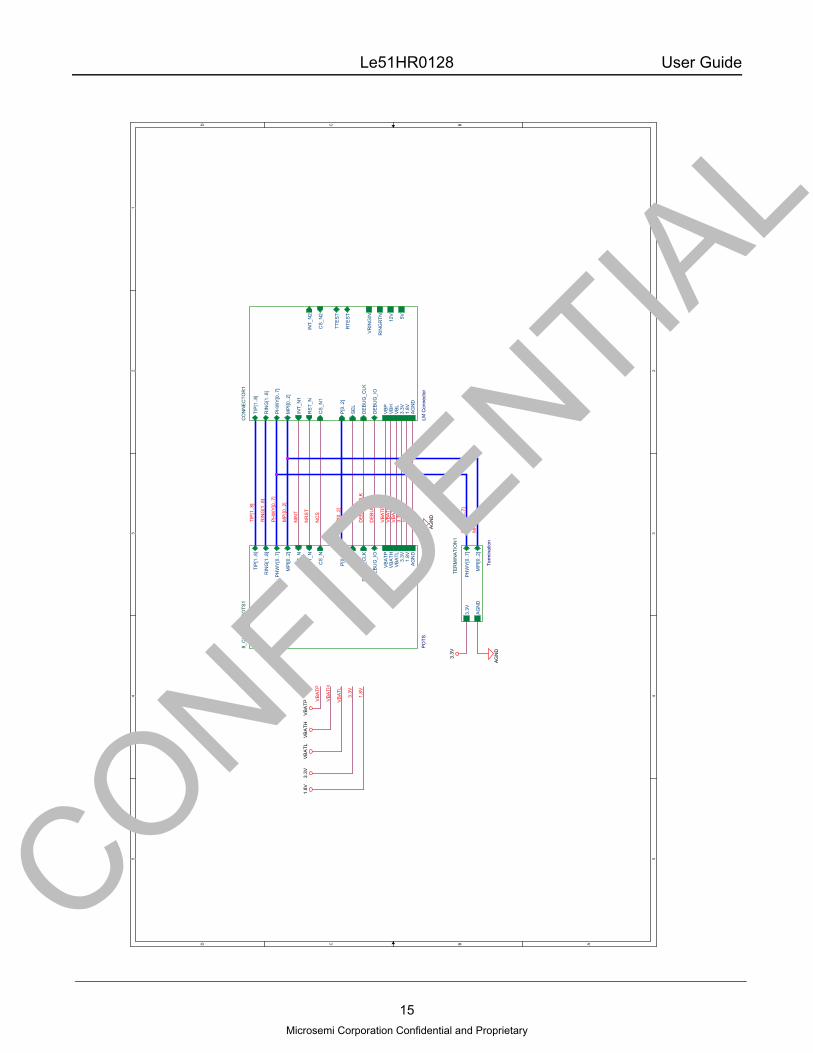
6.0 Schematics and Bill of Materials
Schematics and bill of materials for the Le51HR0128 line module are included on the following pages.
CONFIDENTIAL

Le51HR0128 User Guide
Le51HR0128 Line Module Schematics
5 5
4 4
3 3
2 2
1
DD
CC
BB
A
DIS
CLA
IMER
: TH
IS C
IRC
UIT
DES
IGN
IS P
RO
VID
ED A
S R
EFER
ENC
E O
NLY
, WIT
HO
UT
WA
RR
AN
TY E
XPR
ESSE
D O
R IM
PLIE
D.
THE
USE
R IS
EN
CO
UR
AG
ED T
O P
ERFO
RM
ALL
DU
E D
ILIG
ENC
E W
ITH
RES
PEC
T TO
DES
IGN
AN
D A
NA
LYSI
S.
RoH
S C
ompl
iant
Des
ign
Le51
HR
0128
- 8
Ch
POTS
Lin
e M
odul
eLe
7923
88TV
C N
GC
C S
LAC
Le79
271M
QC
NG
CC
SLI
CTe
st C
onfig
urat
ion
C
CONFIDENTIAL
14
Microsemi Corporation Confidential and Proprietary
Le51HR0128 User Guide
5 5
4 4
3 3
2 2
1
DD
CC
BB
A
3.3V
VB
ATH
VB
ATP
VB
ATL
RIN
G[1
..8]
TIP
[1..8
]
NIN
T
NR
ST
NC
S
1.8V
SE
L
DE
BU
G_C
LK
DE
BU
G_I
O
P[0
..2]
3.3V
VB
ATL
VB
ATH
VB
ATP
1.8V
PH
WY
[0..7
]
MP
I[0..2
]
PH
WY
[0..7
]
MP
I[0..2
]
VB
ATH
VB
ATL
VB
ATP
3.3V
AG
ND
1.8V
AG
ND
3.3V
TER
MIN
ATI
ON
1
Term
inat
ion
AG
ND
3.3V
MP
I[0..2
]
PH
WY
[0..7
]
CO
NN
EC
TOR
1
LM C
onne
ctor
PH
WY
[0..7
]
MP
I[0..2
]
AG
ND
3.3V
VB
HV
BP
5VV
BL
RIN
G[1
..8]
TIP
[1..8
]
INT_
N1
CS
_N2
INT_
N2
RS
T_N
CS
_N1
VR
ING
IN
RIN
GR
TN 12V
1.8V
RTE
ST
TTE
ST
SE
L
DE
BU
G_C
LK
DE
BU
G_I
O
P[0
..2]
8_C
HA
NN
EL_
PO
TS1
PO
TS
VB
ATH
VB
ATL
1.8V
AG
ND
CS
_N
INT_
N
RS
T_N
3.3V
VB
ATP
P[0
..2]
SE
L
DE
BU
G_C
LK
DE
BU
G_I
O
TIP
[1..8
]
RIN
G[1
..8]
MP
I[0..2
]
PH
WY
[0..7
]
CONFIDENTIAL
15
Microsemi Corporation Confidential and Proprietary

Le51HR0128 User Guide
5 5
4 4
3 3
2 2
1
DD
CC
BB
A
SB
P
SB
H
SB
L
VA
8
VB
8
DC
B8
RC
VP
8R
CV
N8
VR
EF8
DC
A8
IMT8
IA8
IB8
LD8
DIN
MP
I2
DC
LKM
PI0
DO
UT
MP
I1
SE
L
SE
L
SE
L
SE
L
SV
A1
SV
B1
DC
B1
RC
VP
1R
CV
N1
VR
EF1
DC
A1
IMT1
IA1
IB1
LD1
SE
L
SE
L
SE
L
TIP
1 TIP
3
TIP
5
RIN
G5
TIP
7
TIP
2
RIN
G2
TIP
4
RIN
G4
TIP
6
RIN
G6
TIP
8
RIN
G8
VA
4
DC
B4
RC
VP
4
VR
EF4
DC
A4
IMT4
IA4
IB4
LD4RC
VN
4
VB
4
VA
7
VB
7
DC
B7
RC
VP
7R
CV
N7
VR
EF7
DC
A7
IMT7
IA7
IB7
LD7
VA
6
VB
6
DC
B6
RC
VP
6R
CV
N6
VR
EF6
DC
A6
IMT6
IA6
IB6
LD6
VB
3
DC
B3
RC
VP
3R
CV
N3
VR
EF3
DC
A3
IMT3
IA3
IB3
LD3 VA
5
VB
5
DC
B5
RC
VP
5R
CV
N5
VR
EF5
DC
A5
IMT5
IA5
IB5
LD5
VA
2
VB
2
DC
B2
RC
VP
2R
CV
N2
VR
EF2
DC
A2
IMT2
IA2
IB2
LD2
P[0
..2]
P[0
..2]
SE
L
SE
L
P[0
..2]
P[0
..2]
P[0
..2]
P[0
..2]
P[0
..2]
P[0
..2]
P[0
..2]
VA
3
RIN
G1
RIN
G[1
..8]
TIP
[1..8
]
MP
I[0..2
]
PH
WY
0FS
PH
WY
1P
CLK
PH
WY
2D
RA
PH
WY
3D
XA
PH
WY
4TS
CA
_NP
HW
Y5
DR
BP
HW
Y6
DX
BP
HW
Y7
TSC
B_N
RIN
G7
RIN
G3
VB
ATH
VB
ATL
1.8V
AG
ND
CS
_NIN
T_N
RS
T_N
3.3V
VB
ATP
P[0
..2]
SE
L
DE
BU
G_C
LKD
EB
UG
_IO
TIP
[1..8
]
RIN
G[1
..8]
MP
I[0..2
]
PH
WY
[0..7
]
AG
ND
VB
ATH
VB
ATL
1.8V
AG
NDV
BA
THV
BA
TLV
BA
TP
VB
ATH
VB
ATL
VB
ATP
VB
ATH
VB
ATL
VB
ATP
VB
ATH
VB
ATL
VB
ATP
VB
ATH
VB
ATL
VB
ATP
VB
ATH
VB
ATL
VB
ATP
VB
ATH
VB
ATL
VB
ATP
VB
ATH
VB
ATL
VB
ATP
VB
ATH
VB
ATL
VB
ATP
3.3V
VB
ATP
3.3V
AG
ND
1.8V
3.3V
3.3V
3.3V
3.3V
3.3V
3.3V
3.3V
3.3V
AG
ND
AG
ND
AG
ND
AG
ND
AG
ND
AG
ND
AG
ND
PHW
Y BU
SPH
WY0
- Fr
ameS
ync
PHW
Y1 -
PCLK
PHW
Y2 -
DR
APH
WY3
- D
XAPH
WY4
-TSC
A_N
PHW
Y5 -
DR
BPH
WY6
- D
XBPH
WY7
- TS
CB_
N
MPI
BU
SM
PI0
- DC
LKM
PI1
- DO
UT
MPI
2 - D
INR
SB
P1
1.62
Meg
RS
BP
11.
62M
eg
SLI
C8
SLI
C
DC
B
RC
VP
VREF
DC
A
VBAT
H
VBAT
L
AVC
C
AGN
D
VBAT
P
P[0.
.2]
IA IB SEL
LDRC
VN
IMT
TIP
RIN
G
SVA
SVB
RS
BH
11.
62M
egR
SB
H1
1.62
Meg
SLI
C4
SLI
C
DC
B
RC
VP
VREF
DC
A
VBAT
H
VBAT
L
AVC
C
AGN
D
VBAT
P
P[0.
.2]
IA IB SEL
LDRC
VN
IMT
TIP
RIN
G
SVA
SVB
SLI
C1
SLI
C
DC
B
RC
VP
VREF
DC
A
VBAT
H
VBAT
L
AVC
C
AGN
D
VBAT
P
P[0.
.2]IA IB
SEL
LD
RC
VN IMT
TIP
RIN
G
SVA
SVB
RS
BL1
1.62
Meg
RS
BL1
1.62
Meg
SLI
C3
SLI
C
DC
B
RC
VP
VREF
DC
A
VBAT
H
VBAT
L
AVC
C
AGN
D
VBAT
P
P[0.
.2]
IA IB SEL
LDRC
VN
IMT
TIP
RIN
G
SVA
SVB
SLI
C7
SLI
C
DC
B
RC
VP
VREF
DC
A
VBAT
H
VBAT
L
AVC
C
AGN
D
VBAT
P
P[0.
.2]IA IB
SEL
LD
RC
VN IMT
TIP
RIN
G
SVA
SVB
NG
CC
_SLA
C1
SLA
C1.8V
AGN
D
3.3V
SEL
P[0.
.2]
SBP
SBH
SBL
PCLK
DXA
DR
AFS
RST
_NIN
T_N
DC
LK DIN
CS_
N
DO
UT
DEB
UG
_CLK
DXB
DR
B
SVA2 IB
2SV
B2
RC
VP2
RC
VN2
RC
VP3
RC
VN3
IMT3
IA3
IB3
IO20
IO21
IO31
IO30
IMT2 IA
2
SVB1
SVA1
RC
VP1
RC
VN1
IMT1
IA1
IB1
IO11
IO10
IB4
RC
VP4
RC
VN4
IO40
IO41
IMT4 IA
4
IB6
RC
VP6
RC
VN6
RC
VP7
RC
VN7
IMT7
IA7
IB7
IO60
IO61
IO71
IO70
IMT6 IA
6
RC
VP5
RC
VN5
IMT5
IA5
IB5
IO51
IO50
RC
VP8
RC
VN8
IMT8 IA
8
IB8
IO81
IO80
TSC
B_N
TSC
A_N
LD8
LD3
LD1
LD2
LD4
LD7
LD5
LD6
DEB
UG
_IO
DC
A1VR
EF1
DC
B1
DC
A2VR
EF2
DC
B2
DC
A3VR
EF3
DC
B3
SVA3
SVB3
DC
A4VR
EF4
DC
B4
SVA4
SVB4
DC
A5VR
EF5
DC
B5
SVA5
SVB5
DC
A6VR
EF6
DC
B6
SVA6
SVB6
DC
A7VR
EF7
DC
B7
SVA7
SVB7
DC
A8VR
EF8
DC
B8
SVA8
SVB8
SLI
C5
SLI
C
DC
B
RC
VP
VREF
DC
A
VBAT
H
VBAT
L
AVC
C
AGN
D
VBAT
P
P[0.
.2]IA IB
SEL
LD
RC
VN IMT
TIP
RIN
G
SVA
SVB
SLI
C2
SLI
C
DC
B
RC
VP
VREF
DC
A
VBAT
H
VBAT
L
AVC
C
AGN
D
VBAT
P
P[0.
.2]IA IB
SEL
LD
RC
VN IMT
TIP
RIN
G
SVA
SVB
SLI
C6
SLI
C
DC
B
RC
VP
VREF
DC
A
VBAT
H
VBAT
L
AVC
C
AGN
D
VBAT
P
P[0.
.2]
IA IB SEL
LDRC
VN
IMT
TIP
RIN
G
SVA
SVB
CONFIDENTIAL
16
Microsemi Corporation Confidential and Proprietary

Le51HR0128 User Guide
5 5
4 4
3 3
2 2
1
DD
CC
BB
A
AV
DD
CA
NC
EL2
IMT2
IRE
F
P0
P1
P2
CA
NC
EL1
IMT1
VA
C1
VA
C2
CA
NC
EL3
IMT3
VA
C3
CA
NC
EL4
IMT4
VA
C4
CA
NC
EL5
IMT5
VIM
T5V
AC
5
CA
NC
EL6
IMT6
VIM
T6V
AC
6
CA
NC
EL7
IMT7
VIM
T7V
AC
7
CA
NC
EL8
IMT8
VIM
T8V
AC
8V
IMT4
VIM
T2
VIM
T1
VIM
T3
AV
DD
IB4
RC
VP
4R
CV
N4
IO40
IO41
IMT4
IA4
LD8
SB
PS
BH
SB
L
DX
BD
RB
LD3
LD1
LD2
LD4
LD7
LD5
LD6
IB6
RC
VP
6R
CV
N6
RC
VP
7R
CV
N7
IMT7
IA7
IB7
IO60
IO61
IO71
IO70
IMT6
IA6
RC
VP
5R
CV
N5
IMT5
IA5
IB5
IO51
IO50
RC
VP
8R
CV
N8
IMT8
IA8
IB8
IO81
IO80
DC
A3
VR
EF3
DC
B3
SV
A3
SV
B3
DC
A8
VR
EF8
DC
B8
SV
A8
SV
B8
DE
BU
G_C
LKD
EB
UG
_IO
DC
A1
DC
A4
VR
EF4
DC
B4
SV
A4
SV
B4
VR
EF1
DC
B1
TSC
B_N
TSC
A_N
DC
A6
VR
EF6
DC
B6
SV
A6
SV
B6
PC
LK
DX
AD
RA
FSRS
T_N
INT_
N
DC
LK
DIN
CS
_N
DO
UT
SE
L
P[0
..2]
DC
A7
VR
EF7
DC
B7
SV
A7
SV
B7
DC
A5
VR
EF5
DC
B5
SV
A5
SV
B5
1.8V
AG
ND
DC
A2
VR
EF2
DC
B2
3.3V
SV
A2
IB2
SV
B2
RC
VP
2R
CV
N2
RC
VP
3R
CV
N3
IMT3
IA3
IB3
IO20
IO21
IO31
IO30
IMT2
IA2
SV
B1
SV
A1
RC
VP
1R
CV
N1
IMT1
IA1IB1
IO11
IO10
3.3V
1.8V
AG
ND
AG
ND
1.8V
AG
ND
1.8V
AG
ND
AG
ND
AG
ND
AG
ND
1.8V
1.8V
1.8V
AG
ND
AG
ND
AG
ND
AG
ND
3.3V
3.3V
3.3V
AG
ND
AG
ND
AG
ND
AG
ND
3.3V
RIM
T54.
02K
RIM
T54.
02K
RIM
T24.
02K
RIM
T24.
02K
CC
AN
32.
2nF
CC
AN
32.
2nF
CA
VD
D1
100n
FC
AV
DD
110
0nF
CV
AC
310
0nF
CV
AC
310
0nF
RIM
T64.
02K
RIM
T64.
02K
RIM
T44.
02K
RIM
T44.
02K
RIM
T14.
02K
RIM
T14.
02K
CC
AN
82.
2nF
CC
AN
82.
2nF
CV
18_1
100n
FC
V18
_110
0nF
U10
Le79
2388
TVC
U10
Le79
2388
TVC
DX
A15
7D
RA
156
FS15
4P
CLK
155
DG
ND
_5
146
DX
B16
0
TSC
A_N
161
TSC
B_N
162
DR
B16
3
SV
A1
166
SV
B1
167
IB1
168
VIM
T116
9V
AC
117
0C
AN
CE
L117
1IM
T117
2IA
117
3D
CA
117
4V
RE
F117
5D
CB
117
6R
CV
N1
1R
CV
P1
2IO
1_1
3IO
1_0
4
SV
A2
6S
VB
27
IB2
8V
IMT2
9V
AC
210
CA
NC
EL2
12IM
T213
IA2
14D
CA
215
VR
EF2
16D
CB
217
RC
VN
218
RC
VP
219
IO2_
120
IO2_
021
SV
A3
24S
VB
325
IB3
26V
IMT3
27V
AC
328
CA
NC
EL3
29IM
T330
IA3
31D
CA
332
VR
EF3
33D
CB
334
RC
VN
336
RC
VP
337
IO3_
138
IO3_
039
SV
A4
41S
VB
442
IB4
43V
IMT4
44V
AC
445
CA
NC
EL4
46IM
T447
IA4
48D
CA
449
VR
EF4
50D
CB
451
RC
VN
452
RC
VP
453
IO4_
154
IO4_
055
LD1
59LD
260
LD3
61LD
462
SE
L68
P0
65P
166
P2
67
LD5
69LD
670
LD7
71LD
872
DE
BU
G_C
LK16
5D
EB
UG
_IO
164
IRE
F23
SV
A5
75S
VB
576
IB5
77V
IMT5
78V
AC
579
CA
NC
EL5
80IM
T581
IA5
82D
CA
583
VR
EF5
84D
CB
585
RC
VN
586
RC
VP
587
IO5_
188
IO5_
089
SV
A6
91S
VB
692
IB6
93V
IMT6
94V
AC
695
CA
NC
EL6
97IM
T698
IA6
99D
CA
610
0V
RE
F610
1D
CB
610
2R
CV
N6
103
RC
VP
610
4IO
6_1
105
IO6_
010
6
SV
A7
111
IB7
113
VIM
T711
4V
AC
711
5C
AN
CE
L711
6IM
T711
7IA
711
8D
CA
711
9V
RE
F712
0D
CB
712
1R
CV
N7
123
RC
VP
712
4IO
7_1
125
IO7_
012
6
SV
A8
128
SV
B8
129
AG
ND
8
143
IB8
130
VIM
T813
1V
AC
813
2C
AN
CE
L813
3IM
T813
4IA
813
5D
CA
813
6V
RE
F813
7D
CB
813
8R
CV
N8
139
RC
VP
814
0IO
8_1
141
IO8_
014
2
RS
T_N
144
INT_
N14
5
DO
UT
148
DIN
149
DC
LK15
0C
S_N
151
VD
D18
_4
159
VD
D18
_1
57
AV
DD
78
122
AV
DD
56
96
VD
D33
_1
63
SLB11
0
SH
B109
SP
B108
VD
D33
_2
153
AV
DD
34
35
AV
DD
12
11
VD
D18
_2
73
DG
ND
_1
158
DG
ND
_2
58
SV
B7
112
AG
ND
7
127
AG
ND
6
107
AG
ND
5
90
DG
ND
_3
64
DG
ND
_4
74
AG
ND
4
56
AG
ND
3
40
AG
ND
2
22
AG
ND
1
5
VD
D18
_3
147
DG
ND
_6
152
CV
AC
810
0nF
CV
AC
810
0nF
RIM
T34.
02K
RIM
T34.
02K
CV
18_4
100n
FC
V18
_410
0nF
CC
AN
72.
2nF
CC
AN
72.
2nF
CV
18_2
100n
FC
V18
_210
0nF
CV
AC
110
0nF
CV
AC
110
0nF
RIM
T84.
02K
RIM
T84.
02K
CV
AC
710
0nF
CV
AC
710
0nF
RR
EF1
75K
0.25
%
RR
EF1
75K
0.25
%
CV
DD
210
0nF
CV
DD
210
0nF
CV
18_3
100n
FC
V18
_310
0nF
CC
AN
12.
2nF
CC
AN
12.
2nF
+
CF1
10uF
DN
P
+
CF1
10uF
DN
P
+
CF2
33uF
DN
P
+
CF2
33uF
DN
P
CA
VD
D4
100n
FC
AV
DD
410
0nF
CC
AN
52.
2nF
CC
AN
52.
2nF
CV
DD
110
0nF
CV
DD
110
0nF
RIM
T74.
02K
RIM
T74.
02K
CA
VD
D3
100n
FC
AV
DD
310
0nF
CV
AC
510
0nF
CV
AC
510
0nF
CV
AC
210
0nF
CV
AC
210
0nF
CC
AN
62.
2nF
CC
AN
62.
2nF
CC
AN
22.
2nF
CC
AN
22.
2nF
CC
AN
42.
2nF
CC
AN
42.
2nF
RF1
0 O
hmR
F10
Ohm
CV
AC
610
0nF
CV
AC
610
0nF
CA
VD
D2
100n
FC
AV
DD
210
0nF
CV
AC
410
0nF
CV
AC
410
0nF
CONFIDENTIAL
17
Microsemi Corporation Confidential and Proprietary

Le51HR0128 User Guide
5 5
4 4
3 3
2 2
1
DD
CC
BB
A
RE
FP
[0..2
]
P1
P2
P0
DC
B
VR
EF
DC
A
VB
ATH
VB
ATL
AV
CC
AG
ND
VB
ATP
P[0
..2]
IA IB SE
L
LD
SV
B
SV
A
TIP
RIN
G
RC
VP
RC
VN
IMT
VB
ATH
VB
ATL
VB
ATH
VB
ATL
VB
ATP
VB
ATP
AV
CC
AV
CC
AG
ND
AG
ND
AG
ND
AG
ND
AG
ND
AG
ND
VB
ATH
VB
ATP
AG
ND
AG
ND
AG
ND
AG
ND
AG
ND
AG
ND
AG
ND
AG
ND
Pin
1P
in2
Pin
3
BA
S21
TFO
OTP
RIN
T - S
OT5
23
CD
CA
122
0nF
CD
CA
122
0nF
CD
CB
122
0nF
CD
CB
122
0nF
RC
VP
156
2R
CV
P1
562
RIV
A1
1.62
Meg
RIV
A1
1.62
Meg
CB
ATL
110
0nF
CB
ATL
110
0nF
RIR
EF1
49.9
KR
IRE
F149
.9K
UP
1
TIS
P91
10L
UP
1
TIS
P91
10L
LIN
E1
1
LIN
E2
4
GN
D6
GN
D7
G1-
2G
2+3
NC
15
NC
28
PTC
1
50 O
hms
PTC
1
50 O
hms
RIV
B2
1.62
Meg
RIV
B2
1.62
Meg
CD
CA
222
0nF
DN
P
CD
CA
222
0nF
DN
P
RC
VN
156
2R
CV
N1
562
CB
ATP
1
220n
F
CB
ATP
1
220n
F
CAD1
4.7n
FCA
D14.
7nF
CB
ATH
1
220n
F
CB
ATH
1
220n
F
CBD1
4.7n
FCB
D14.
7nF
RIV
A2
1.62
Meg
RIV
A2
1.62
Meg
CV
RE
F147
0nF
CV
RE
F147
0nF
U1
Le79
271M
QC
U1
Le79
271M
QC
VB
L18
RIR
EF
6
IA7
VC
C22
NC
110
VB
H16
VB
P20
NC
212
AD
11
NC
315
BD
13
NC
417
TLD
14
IB9
IMT
8
RC
VN
2
DC
A5
NC
519
DC
B3
RC
VP
1
SE
L23
P0
24P
125
P2
26
LD27
AG
ND
28
VR
EF
4
BG
ND
21
EP
AD
29
RTE
ST1
2.0K
RTE
ST1
2.0K
RIV
B1
1.62
Meg
RIV
B1
1.62
Meg
DV
BH
1D
VB
H1
13
2
CA
VC
C1
100n
FC
AV
CC
110
0nF
CV
BH
110
0nF
CV
BH
110
0nF
CD
CB
222
0nF
DN
P
CD
CB
222
0nF
DN
P
CM
14.
7nF
CM
14.
7nF
CONFIDENTIAL
18
Microsemi Corporation Confidential and Proprietary

Le51HR0128 User Guide
5 5
4 4
3 3
2 2
1
DD
CC
BB
A
REF
P[0.
.2]
P1 P2P0
DC
B
VREF
DC
A
VBAT
H
VBAT
L
AVC
C
AGN
D
VBAT
P
P[0.
.2]
IA IB SEL
LD
SVB
SVA
TIP
RIN
G
RC
VP
RC
VN
IMT
VBAT
HVB
ATL
VBAT
HVB
ATL
VBAT
P
VBAT
P
AVC
C
AVC
C
AGN
D
AGN
D
AGN
DAG
ND
AGN
DAG
ND
VBAT
HVB
ATP
AGN
D
AGN
DAG
ND
AGN
D
AGN
D
AGN
D
AGN
D
AGN
D
Pin1
Pin2
Pin3
BAS2
1TFO
OTP
RIN
T - S
OT5
23
CD
CA5
220n
FC
DC
A522
0nF
CD
CB5
220n
FC
DC
B522
0nF
RC
VP3
562
RC
VP3
562
RIV
A51.
62M
egR
IVA5
1.62
Meg
CBA
TL3
100n
FC
BATL
310
0nF
RIR
EF3
49.9
KR
IREF
349
.9K
UP3
TISP
9110
L
UP3
TISP
9110
L
LIN
E11
LIN
E2
4
GN
D6
GN
D7
G1-
2G
2+3
NC
15
NC
28
PTC
3
50 O
hms
PTC
3
50 O
hms
RIV
B61.
62M
egR
IVB6
1.62
Meg
CD
CA6
220n
FD
NP
CD
CA6
220n
FD
NP
RC
VN3
562
RC
VN3
562
CBA
TP3
220n
F
CBA
TP3
220n
F
CAD3
4.7n
FCA
D34.
7nF
CBA
TH3
220n
F
CBA
TH3
220n
F
CBD3
4.7n
FCB
D34.
7nF
RIV
A61.
62M
egR
IVA6
1.62
Meg
CVR
EF3
470n
FC
VREF
347
0nF
U3
Le79
271M
QC
U3
Le79
271M
QC
VBL18
RIR
EF6
IA7
VCC22
NC
110
VBH16
VBP20
NC
212
AD11
NC
315
BD13
NC
417
TLD
14
IB9
IMT
8
RC
VN2
DC
A5
NC
519
DC
B3
RC
VP1
SEL
23
P024
P125
P226
LD27
AGN
D
28
VREF
4
BGN
D
21
EPAD 29
RTE
ST3
2.0K
RTE
ST3
2.0K
RIV
B51.
62M
egR
IVB5
1.62
Meg
DVB
H3
DVB
H3
13
2
CAV
CC
310
0nF
CAV
CC
310
0nF
CVB
H3
100n
FC
VBH
310
0nF
CD
CB6
220n
FD
NP
CD
CB6
220n
FD
NP
CM
34.
7nF
CM
34.
7nF
CONFIDENTIAL
19
Microsemi Corporation Confidential and Proprietary

Le51HR0128 User Guide
5 5
4 4
3 3
2 2
1
DD
CC
BB
A
RE
FP
[0..2
]
P1
P2
P0
DC
B
VR
EF
DC
A
VB
ATH
VB
ATL
AV
CC
AG
ND
VB
ATP
P[0
..2]
IA IB SE
L
LD
SV
B
SV
A
TIP
RIN
G
RC
VP
RC
VN
IMT
VB
ATH
VB
ATL
VB
ATH
VB
ATL
VB
ATP
VB
ATP
AV
CC
AV
CC
AG
ND
AG
ND
AG
ND
AG
ND
AG
ND
AG
ND
VB
ATH
VB
ATP
AG
ND
AG
ND
AG
ND
AG
ND
AG
ND
AG
ND
AG
ND
AG
ND
Pin1
Pin2
Pin3
BAS2
1TFO
OTP
RIN
T - S
OT5
23
CD
CA
322
0nF
CD
CA
322
0nF
CD
CB
322
0nF
CD
CB
322
0nF
RC
VP
256
2R
CV
P2
562
RIV
A3
1.62
Meg
RIV
A3
1.62
Meg
CB
ATL
210
0nF
CB
ATL
210
0nF
RIR
EF2
49.9
KR
IRE
F249
.9K
UP
2
TIS
P91
10L
UP
2
TIS
P91
10L
LIN
E1
1
LIN
E2
4
GN
D6
GN
D7
G1-
2G
2+3
NC
15
NC
28
PTC
2
50 O
hms
PTC
2
50 O
hms
RIV
B4
1.62
Meg
RIV
B4
1.62
Meg
CD
CA
422
0nF
DN
P
CD
CA
422
0nF
DN
P
RC
VN
256
2R
CV
N2
562
CB
ATP
2
220n
F
CB
ATP
2
220n
F
CAD2
4.7n
FCA
D24.
7nF
CB
ATH
2
220n
F
CB
ATH
2
220n
F
CBD2
4.7n
FCB
D24.
7nF
RIV
A4
1.62
Meg
RIV
A4
1.62
Meg
CV
RE
F247
0nF
CV
RE
F247
0nF
U2
Le79
271M
QC
U2
Le79
271M
QC
VB
L18
RIR
EF
6
IA7
VC
C22
NC
110
VB
H16
VB
P20
NC
212
AD
11
NC
315
BD
13
NC
417
TLD
14
IB9
IMT
8
RC
VN
2
DC
A5
NC
519
DC
B3
RC
VP
1
SE
L23
P0
24P
125
P2
26
LD27
AG
ND
28
VR
EF
4
BG
ND
21
EP
AD
29
RTE
ST2
2.0K
RTE
ST2
2.0K
RIV
B3
1.62
Meg
RIV
B3
1.62
Meg
DV
BH
2D
VB
H2
13
2
CA
VC
C2
100n
FC
AV
CC
210
0nF
CV
BH
210
0nF
CV
BH
210
0nF
CD
CB
422
0nF
DN
P
CD
CB
422
0nF
DN
P
CM
24.
7nF
CM
24.
7nF
CONFIDENTIAL
20
Microsemi Corporation Confidential and Proprietary

Le51HR0128 User Guide
5 5
4 4
3 3
2 2
1
DD
CC
BB
A
REF
P[0.
.2]
P1 P2P0
DC
B
VREF
DC
A
VBAT
H
VBAT
L
AVC
C
AGN
D
VBAT
P
P[0.
.2]
IA IB SEL
LD
SVB
SVA
TIP
RIN
G
RC
VP
RC
VN
IMT
VBAT
HVB
ATL
VBAT
HVB
ATL
VBAT
P
VBAT
P
AVC
C
AVC
C
AGN
D
AGN
D
AGN
DAG
ND
AGN
DAG
ND
VBAT
HVB
ATP
AGN
D
AGN
DAG
ND
AGN
D
AGN
D
AGN
D
AGN
D
AGN
D
Pin1
Pin2
Pin3
BAS2
1TFO
OTP
RIN
T - S
OT5
23
CD
CA7
220n
FC
DC
A722
0nF
CD
CB7
220n
FC
DC
B722
0nF
RC
VP4
562
RC
VP4
562
RIV
A71.
62M
egR
IVA7
1.62
Meg
CBA
TL4
100n
FC
BATL
410
0nF
RIR
EF4
49.9
KR
IREF
449
.9K
UP4
TISP
9110
L
UP4
TISP
9110
L
LIN
E11
LIN
E2
4
GN
D6
GN
D7
G1-
2G
2+3
NC
15
NC
28
PTC
4
50 O
hms
PTC
4
50 O
hms
RIV
B81.
62M
egR
IVB8
1.62
Meg
CD
CA8
220n
FD
NP
CD
CA8
220n
FD
NP
RC
VN4
562
RC
VN4
562
CBA
TP4
220n
F
CBA
TP4
220n
F
CAD4
4.7n
FCA
D44.
7nF
CBA
TH4
220n
F
CBA
TH4
220n
F
CBD4
4.7n
FCB
D44.
7nF
RIV
A81.
62M
egR
IVA8
1.62
Meg
CVR
EF4
470n
FC
VREF
447
0nF
U4
Le79
271M
QC
U4
Le79
271M
QC
VBL18
RIR
EF6
IA7
VCC22
NC
110
VBH16
VBP20
NC
212
AD11
NC
315
BD13
NC
417
TLD
14
IB9
IMT
8
RC
VN2
DC
A5
NC
519
DC
B3
RC
VP1
SEL
23
P024
P125
P226
LD27
AGN
D
28
VREF
4
BGN
D
21
EPAD 29
RTE
ST4
2.0K
RTE
ST4
2.0K
RIV
B71.
62M
egR
IVB7
1.62
Meg
DVB
H4
DVB
H4
13
2
CAV
CC
410
0nF
CAV
CC
410
0nF
CVB
H4
100n
FC
VBH
410
0nF
CD
CB8
220n
FD
NP
CD
CB8
220n
FD
NP
CM
44.
7nF
CM
44.
7nF
CONFIDENTIAL
21
Microsemi Corporation Confidential and Proprietary

Le51HR0128 User Guide
5 5
4 4
3 3
2 2
1
DD
CC
BB
A
REF
P[0.
.2]
P1 P2P0
DC
B
VREF
DC
A
VBAT
H
VBAT
L
AVC
C
AGN
D
VBAT
P
P[0.
.2]
IA IB SEL
LD
SVB
SVA
TIP
RIN
G
RC
VP
RC
VN
IMT
VBAT
HVB
ATL
VBAT
HVB
ATL
VBAT
P
VBAT
P
AVC
C
AVC
C
AGN
D
AGN
D
AGN
DAG
ND
AGN
DAG
ND
VBAT
HVB
ATP
AGN
D
AGN
DAG
ND
AGN
D
AGN
D
AGN
D
AGN
D
AGN
D
Pin1
Pin2
Pin3
BAS2
1TFO
OTP
RIN
T - S
OT5
23
CD
CA9
220n
FC
DC
A922
0nF
CD
CB9
220n
FC
DC
B922
0nF
RC
VP5
562
RC
VP5
562
RIV
A91.
62M
egR
IVA9
1.62
Meg
CBA
TL5
100n
FC
BATL
510
0nF
RIR
EF5
49.9
KR
IREF
549
.9K
UP5
TISP
9110
L
UP5
TISP
9110
L
LIN
E11
LIN
E2
4
GN
D6
GN
D7
G1-
2G
2+3
NC
15
NC
28
PTC
5
50 O
hms
PTC
5
50 O
hms
RIV
B10
1.62
Meg
RIV
B10
1.62
Meg
CD
CA1
022
0nF
DN
P
CD
CA1
022
0nF
DN
P
RC
VN5
562
RC
VN5
562
CBA
TP5
220n
F
CBA
TP5
220n
F
CAD5
4.7n
FCA
D54.
7nF
CBA
TH5
220n
F
CBA
TH5
220n
F
CBD5
4.7n
FCB
D54.
7nF
RIV
A10
1.62
Meg
RIV
A10
1.62
Meg
CVR
EF5
470n
FC
VREF
547
0nF
U5
Le79
271M
QC
U5
Le79
271M
QC
VBL18
RIR
EF6
IA7
VCC22
NC
110
VBH16
VBP20
NC
212
AD11
NC
315
BD13
NC
417
TLD
14
IB9
IMT
8
RC
VN2
DC
A5
NC
519
DC
B3
RC
VP1
SEL
23
P024
P125
P226
LD27
AGN
D
28
VREF
4
BGN
D
21
EPAD 29
RTE
ST5
2.0K
RTE
ST5
2.0K
RIV
B91.
62M
egR
IVB9
1.62
Meg
DVB
H5
DVB
H5
13
2
CAV
CC
510
0nF
CAV
CC
510
0nF
CVB
H5
100n
FC
VBH
510
0nF
CD
CB1
022
0nF
DN
P
CD
CB1
022
0nF
DN
P
CM
54.
7nF
CM
54.
7nF
CONFIDENTIAL
22
Microsemi Corporation Confidential and Proprietary

Le51HR0128 User Guide
5 5
4 4
3 3
2 2
1
DD
CC
BB
A
REF
P[0.
.2]
P1 P2P0
DC
B
VREF
DC
A
VBAT
H
VBAT
L
AVC
C
AGN
D
VBAT
P
P[0.
.2]
IA IB SEL
LD
SVB
SVA
TIP
RIN
G
RC
VP
RC
VN
IMT
VBAT
HVB
ATL
VBAT
HVB
ATL
VBAT
P
VBAT
P
AVC
C
AVC
C
AGN
D
AGN
D
AGN
DAG
ND
AGN
DAG
ND
VBAT
HVB
ATP
AGN
D
AGN
DAG
ND
AGN
D
AGN
D
AGN
D
AGN
D
AGN
D
Pin1
Pin2
Pin3
BAS2
1TFO
OTP
RIN
T - S
OT5
23
CD
CA1
122
0nF
CD
CA1
122
0nF
CD
CB1
122
0nF
CD
CB1
122
0nF
RC
VP6
562
RC
VP6
562
RIV
A11
1.62
Meg
RIV
A11
1.62
Meg
CBA
TL6
100n
FC
BATL
610
0nF
RIR
EF6
49.9
KR
IREF
649
.9K
UP6
TISP
9110
L
UP6
TISP
9110
L
LIN
E11
LIN
E2
4
GN
D6
GN
D7
G1-
2G
2+3
NC
15
NC
28
PTC
6
50 O
hms
PTC
6
50 O
hms
RIV
B12
1.62
Meg
RIV
B12
1.62
Meg
CD
CA1
222
0nF
DN
P
CD
CA1
222
0nF
DN
P
RC
VN6
562
RC
VN6
562
CBA
TP6
220n
F
CBA
TP6
220n
F
CAD6
4.7n
FCA
D64.
7nF
CBA
TH6
220n
F
CBA
TH6
220n
F
CBD6
4.7n
FCB
D64.
7nF
RIV
A12
1.62
Meg
RIV
A12
1.62
Meg
CVR
EF6
470n
FC
VREF
647
0nF
U6
Le79
271M
QC
U6
Le79
271M
QC
VBL18
RIR
EF6
IA7
VCC22
NC
110
VBH16
VBP20
NC
212
AD11
NC
315
BD13
NC
417
TLD
14
IB9
IMT
8
RC
VN2
DC
A5
NC
519
DC
B3
RC
VP1
SEL
23
P024
P125
P226
LD27
AGN
D
28
VREF
4
BGN
D
21
EPAD 29
RTE
ST6
2.0K
RTE
ST6
2.0K
RIV
B11
1.62
Meg
RIV
B11
1.62
Meg
DVB
H6
DVB
H6
13
2
CAV
CC
610
0nF
CAV
CC
610
0nF
CVB
H6
100n
FC
VBH
610
0nF
CD
CB1
222
0nF
DN
P
CD
CB1
222
0nF
DN
P
CM
64.
7nF
CM
64.
7nF
CONFIDENTIAL
23
Microsemi Corporation Confidential and Proprietary

Le51HR0128 User Guide
5 5
4 4
3 3
2 2
1
DD
CC
BB
A
REF
P[0.
.2]
P1 P2P0
DC
B
VREF
DC
A
VBAT
H
VBAT
L
AVC
C
AGN
D
VBAT
P
P[0.
.2]
IA IB SEL
LD
SVB
SVA
TIP
RIN
G
RC
VP
RC
VN
IMT
VBAT
HVB
ATL
VBAT
HVB
ATL
VBAT
P
VBAT
P
AVC
C
AVC
C
AGN
D
AGN
D
AGN
DAG
ND
AGN
DAG
ND
VBAT
HVB
ATP
AGN
D
AGN
DAG
ND
AGN
D
AGN
D
AGN
D
AGN
D
AGN
D
Pin1
Pin2
Pin3
BAS2
1TFO
OTP
RIN
T - S
OT5
23
CD
CA1
322
0nF
CD
CA1
322
0nF
CD
CB1
322
0nF
CD
CB1
322
0nF
RC
VP7
562
RC
VP7
562
RIV
A13
1.62
Meg
RIV
A13
1.62
Meg
CBA
TL7
100n
FC
BATL
710
0nF
RIR
EF7
49.9
KR
IREF
749
.9K
UP7
TISP
9110
L
UP7
TISP
9110
L
LIN
E11
LIN
E2
4
GN
D6
GN
D7
G1-
2G
2+3
NC
15
NC
28
PTC
7
50 O
hms
PTC
7
50 O
hms
RIV
B14
1.62
Meg
RIV
B14
1.62
Meg
CD
CA1
422
0nF
DN
P
CD
CA1
422
0nF
DN
P
RC
VN7
562
RC
VN7
562
CBA
TP7
220n
F
CBA
TP7
220n
F
CAD7
4.7n
FCA
D74.
7nF
CBA
TH7
220n
F
CBA
TH7
220n
F
CBD7
4.7n
FCB
D74.
7nF
RIV
A14
1.62
Meg
RIV
A14
1.62
Meg
CVR
EF7
470n
FC
VREF
747
0nF
U7
Le79
271M
QC
U7
Le79
271M
QC
VBL18
RIR
EF6
IA7
VCC22
NC
110
VBH16
VBP20
NC
212
AD11
NC
315
BD13
NC
417
TLD
14
IB9
IMT
8
RC
VN2
DC
A5
NC
519
DC
B3
RC
VP1
SEL
23
P024
P125
P226
LD27
AGN
D
28
VREF
4
BGN
D
21
EPAD 29
RTE
ST7
2.0K
RTE
ST7
2.0K
RIV
B13
1.62
Meg
RIV
B13
1.62
Meg
DVB
H7
DVB
H7
13
2
CAV
CC
710
0nF
CAV
CC
710
0nF
CVB
H7
100n
FC
VBH
710
0nF
CD
CB1
422
0nF
DN
P
CD
CB1
422
0nF
DN
P
CM
74.
7nF
CM
74.
7nF
CONFIDENTIAL
24
Microsemi Corporation Confidential and Proprietary

Le51HR0128 User Guide
5 5
4 4
3 3
2 2
1
DD
CC
BB
A
REF
P[0.
.2]
P1 P2P0
DC
B
VREF
DC
A
VBAT
H
VBAT
L
AVC
C
AGN
D
VBAT
P
P[0.
.2]
IA IB SEL
LD
SVB
SVA
TIP
RIN
G
RC
VP
RC
VN
IMT
VBAT
HVB
ATL
VBAT
HVB
ATL
VBAT
P
VBAT
P
AVC
C
AVC
C
AGN
D
AGN
D
AGN
DAG
ND
AGN
DAG
ND
VBAT
HVB
ATP
AGN
D
AGN
DAG
ND
AGN
D
AGN
D
AGN
D
AGN
D
AGN
D
Pin1
Pin2
Pin3
BAS2
1TFO
OTP
RIN
T - S
OT5
23
CD
CA1
522
0nF
CD
CA1
522
0nF
CD
CB1
522
0nF
CD
CB1
522
0nF
RC
VP8
562
RC
VP8
562
RIV
A15
1.62
Meg
RIV
A15
1.62
Meg
CBA
TL8
100n
FC
BATL
810
0nF
RIR
EF8
49.9
KR
IREF
849
.9K
UP8
TISP
9110
L
UP8
TISP
9110
L
LIN
E11 LIN
E2
4
GN
D6
GN
D7
G1-
2G
2+3
NC
15
NC
28
PTC
8
50 O
hms
PTC
8
50 O
hms
RIV
B16
1.62
Meg
RIV
B16
1.62
Meg
CD
CA1
622
0nF
DN
P
CD
CA1
622
0nF
DN
P
RC
VN8
562
RC
VN8
562
CBA
TP8
220n
F
CBA
TP8
220n
F
CAD8
4.7n
FCA
D84.
7nF
CBA
TH8
220n
F
CBA
TH8
220n
F
CBD8
4.7n
FCB
D84.
7nF
RIV
A16
1.62
Meg
RIV
A16
1.62
Meg
CVR
EF8
470n
FC
VREF
847
0nF
U8
Le79
271M
QC
U8
Le79
271M
QC
VBL18
RIR
EF6
IA7
VCC22
NC
110
VBH16
VBP20
NC
212
AD11
NC
315
BD13
NC
417
TLD
14
IB9
IMT
8
RC
VN2
DC
A5
NC
519
DC
B3
RC
VP1
SEL
23
P024
P125
P226
LD27
AGN
D
28
VREF
4
BGN
D
21
EPAD 29
RTE
ST8
2.0K
RTE
ST8
2.0K
RIV
B15
1.62
Meg
RIV
B15
1.62
Meg
DVB
H8
DVB
H8
13
2
CAV
CC
810
0nF
CAV
CC
810
0nF
CVB
H8
100n
FC
VBH
810
0nF
CD
CB1
622
0nF
DN
P
CD
CB1
622
0nF
DN
P
CM
84.
7nF
CM
84.
7nF
CONFIDENTIAL
25
Microsemi Corporation Confidential and Proprietary

Le51HR0128 User Guide
5 5
4 4
3 3
2 2
1
DD
CC
BB
A
RST
_ND
OU
TM
PI1
DC
LKM
PI0
CS_
N1
FSPH
WY0
TSC
B_N
PHW
Y7
PHW
Y[0.
.7]
DR
APH
WY2
DXB
PHW
Y6
MPI
[0..2
]
P0 P2
PHW
Y[0.
.7]
INT_
N1
INT_
N2
DIN
MPI
2C
S_N
2PC
LKPH
WY1
DXA
PHW
Y3TS
CA_
NPH
WY4
DR
BPH
WY5
MPI
[0..2
]
IDC
S
P1SE
L
RIN
G5
RIN
G6
RIN
G7
RIN
G8
RIN
G[1
..8]
TIP[
1..8
]TI
P5TI
P6TI
P7TI
P8
TIP[
1..8
]TI
P1TI
P2TI
P3TI
P4
RIN
G1
RIN
G2
RIN
G3
RIN
G4
RIN
G[1
..8]
P[0.
.2]
P[0.
.2]
DEB
UG
_IO
DEB
UG
_CLK
PHW
Y[0.
.7]
MPI
[0..2
]
AGN
D
3.3V
VBH
VBP
5V VBL
RIN
G[1
..8]
TIP[
1..8
]
INT_
N1
CS_
N2
INT_
N2
RST
_N
CS_
N1
VRIN
GIN
RIN
GR
TN
12V
1.8V
RTE
STTT
EST
SEL
DEB
UG
_IO
DEB
UG
_CLK
P[0.
.2]
AGN
DAG
ND
AGN
D
1.8V
AGN
D
PHW
Y BU
SPH
WY0
- Fr
ameS
ync
PHW
Y1 -
PCLK
PHW
Y2 -
DR
APH
WY3
- D
XAPH
WY4
-TSC
A_N
PHW
Y5 -
DR
BPH
WY6
- D
XBPH
WY7
- TS
CB_
N
MPI
BU
SM
PI0
- DC
LKM
PI1
- DO
UT
MPI
2 - D
IN
U9 DS2
433S
+IC
U9 DS2
433S
+IC
NC
11
NC
22
NC
35
NC
46
NC
57
Dat
a3
GN
D4
NC
68
P1
ASP-
1324
89-0
1
P1
ASP-
1324
89-0
11 3 5 7 9 11 13 15 17 19 21 23 25 27 29 31 33 35 37 39 41 43 45 47 49 51 53 55 57 59
2 4 6 8 10 12 14 16 18 20 22 24 26 28 30 32 34 36 38 40 42 44 46 48 50 52 54 56 58 60 RD
OW
N1
10.0
KR
DO
WN
110
.0K
RU
P110
.0K
RU
P110
.0K
CONFIDENTIAL
26
Microsemi Corporation Confidential and Proprietary

Le51HR0128 User Guide
5 5
4 4
3 3
2 2
1
DD
CC
BB
A
PHW
Y0FS
PHW
Y5D
RB
PHW
Y2D
RA
PHW
Y1PC
LK
MPI
0D
CLK
MPI
2D
IN
PHW
Y[0.
.7]
MPI
[0..2
]M
PI[0
..2]
AGN
D
3.3V
PHW
Y[0.
.7]
AGN
DAG
ND
AGN
DAG
ND
AGN
D
3.3V
3.3V
3.3V
3.3V
AGN
DAG
ND
PHW
Y BU
SPH
WY0
- Fr
ameS
ync
PHW
Y1 -
PCLK
PHW
Y2 -
DR
APH
WY3
- D
XAPH
WY4
-TSC
A_N
PHW
Y5 -
DR
BPH
WY6
- D
XBPH
WY7
- TS
CB_
N
MPI
BU
SM
PI0
- DC
LKM
PI1
- DO
UT
MPI
2 - D
IN
RTR
M3
150
DN
P
RTR
M3
150
DN
P
RTR
M8
82.5
RTR
M8
82.5
CTR
M5
12pF
DN
P
CTR
M5
12pF
DN
P
CTR
M1
12pF
DN
P
CTR
M1
12pF
DN
P
RTR
M7
82.5
RTR
M7
82.5
CTR
M4
12pF
DN
P
CTR
M4
12pF
DN
P
RTR
M1
150
DN
P
RTR
M1
150
DN
P
RTR
M6
82.5
RTR
M6
82.5
CTR
M3
12pF
DN
P
CTR
M3
12pF
DN
P
RTR
M4
82.5
RTR
M4
82.5
RTR
M5
82.5
RTR
M5
82.5
CTR
M2
12pF
DN
P
CTR
M2
12pF
DN
P
RTR
M2
150
DN
P
RTR
M2
150
DN
P
RTR
M9
82.5
RTR
M9
82.5
CTR
M6
12pF
DN
P
CTR
M6
12pF
DN
P
CONFIDENTIAL
27
Microsemi Corporation Confidential and Proprietary

Le51HR0128 User Guide
B R
NGCC
8 C
hann
el P
OTS
- Fr
eniu
m R
evise
d: F
riday
, Apr
il 18,
200
8Le
51HR
0128
R
evisi
on: 3
.0DI
SCLA
IMER
: THI
S CI
RCUI
T DE
SIG
N IS
PRO
VIDE
D AS
REF
EREN
CE O
NLY,
WIT
HOUT
WAR
RANT
Y EX
PRES
SED
OR
IMPL
IED.
ZARL
INK
- PP
C21
36 N
orth
13t
h St
Suite
DRe
adin
g, P
a 19
604
Bill O
f Mat
eria
ls
April
18,
2008
10:0
0:12
Item
Qua
ntity
Refe
renc
ePa
rtM
anuf
actu
rer
Part
Num
ber
Dist
ribut
orDi
st P
art N
umbe
rTo
lera
nce
Volta
geCu
rrent
Powe
rTy
peRo
HSNo
tes
116
CBD1
,CAD
1,CB
D2,C
AD2,
CBD3
,CAD
3,CB
D4,C
AD4,
CBD5
,CAD
5,CB
D6,C
AD6,
CBD7
,CAD
7,CB
D8,C
AD8
4.7n
FSy
fer
0603
Y200
0472
KXT
Mou
ser
843-
0603
Y200
0472
K10
%10
0VX7
RYe
s
218
CVDD
1,CA
VDD1
,CAV
CC1,
CVDD
2,CA
VDD2
,CAV
CC2,
CAVD
D3,C
AVCC
3,CA
VDD4
,CAV
CC4,
CAVC
C5,C
AVC
C6,C
AVCC
7,CA
VCC8
,CV1
8_1,
CV18
_2,C
V18_
3,CV
18_4
100n
FKe
met
C040
2C10
4M9R
ACTU
Mou
ser
80-C
0402
C104
M9R
20%
6.3V
X7R
Yes
316
CBAT
P1,C
BATH
1,CB
ATP2
,CBA
TH2,
CBAT
P3,C
BATH
3,CB
ATP4
,CBA
TH4,
CBAT
P5,C
BATH
5,CB
ATP6
,CB
ATH6
,CBA
TP7,
CBAT
H7,C
BATP
8,CB
ATH8
220n
FKe
met
C080
5C22
4M1R
ACTU
Mou
ser
80-C
0805
C224
M1R
20%
100V
X7R
Yes
48
CBAT
L1,C
BATL
2,CB
ATL3
,CBA
TL4,
CBAT
L5,C
BATL
6,CB
ATL7
,CBA
TL8
100n
FM
urat
aG
RM18
8R72
A104
KA35
DDi
gike
y49
0-32
85-1
-ND
10%
100V
X7R
Yes
58
CCAN
1,CC
AN2,
CCAN
3,CC
AN4,
CCAN
5,CC
AN6,
CCAN
7,CC
AN8
2.2n
FKe
met
C040
2C22
2K4R
ACTU
Mou
ser
80-C
0402
C222
K4R
10%
16V
X7R
Yes
616
CDCB
1,CD
CA1,
CDCB
3,CD
CA3,
CDCB
5,CD
CA5,
CDCB
7,CD
CA7,
CDCB
9,CD
CA9,
CDCB
11,C
DCA1
1,CD
C13
,CDC
A13,
CDCB
15,C
DCA1
522
0nF
Taiyo
Yud
enJM
K105
BJ22
4KV-
FNe
wark
86H5
617
10%
6.3V
X7R
Yes
716
CDCB
2,CD
CA2,
CDCB
4,CD
CA4,
CDCB
6,CD
CA6,
CDCB
8,CD
CA8,
CDCB
10,C
DCA1
0,CD
CB12
,CDC
A12,
C DCB
14,C
DCA1
4,CD
CB16
,CDC
A16
220n
FTa
iyo Y
uden
JMK1
05BJ
224K
V-F
Newa
rk86
H561
710
%6.
3VX7
RYe
sDN
P8
1CF
110
uFAV
XTA
JA10
6K00
6RDi
gike
y47
8-16
53-1
-ND
10%
6.3V
Tant
Yes
DNP
91
CF2
33uF
AVX
TAJA
336K
006R
Digi
key
478-
1666
-1-N
D10
%6.
3VTa
ntYe
sDN
P10
8CM
1,CM
2,CM
3,CM
4,CM
5,CM
6,CM
7,CM
84.
7nF
Kem
etC0
402C
472K
3RAC
TUDi
gike
y39
9-10
35-1
-ND
10%
25V
X7R
Yes
116
CTRM
1,CT
RM2,
CTRM
3,CT
RM4,
CTRM
5,CT
RM6
12pF
Kem
etC0
603C
120J
5GAC
TUDi
gike
y39
9-10
50-1
-ND
5%50
VNP
OYe
sDN
P12
8CV
AC1,
CVAC
2,CV
AC3,
CVAC
4,CV
AC5,
CVAC
6,CV
AC7,
CVAC
810
0nF
Mur
ata
GRM
155R
71C1
04KA
88D
Digi
key
490-
3261
-1-N
D10
%10
VX7
RYe
s13
8CV
BH1,
CVBH
2,CV
BH3,
CVBH
4,CV
BH5,
CVBH
6,CV
BH7,
CVBH
810
0nF
Kem
etC0
805C
104K
1RAC
TUDi
giKe
y39
9-34
86-1
-ND
10%
100V
X7R
Yes
148
CVRE
F1,C
VREF
2,CV
REF3
,CVR
EF4,
CVRE
F5,C
VREF
6,CV
REF7
,CVR
EF8
470n
FKe
met
C060
3C47
4K4R
ACTU
Mou
ser
80-C
0603
C474
K4R
10%
16V
X7R
Yes
158
DVBH
1,DV
BH2,
DVBH
3,DV
BH4,
DVBH
5,DV
BH6,
DVBH
7,DV
BH8
BAS2
1T_7
_F_R
oHS
Diod
es In
cBA
S21T
-7-F
Digi
key
BAS2
1T-F
DITR
-ND
Yes
168
PTC1
,PTC
2,PT
C3,P
TC4,
PTC5
,PTC
6,PT
C7,P
TC8
50 O
hms
Bour
nsCM
F-SD
50Ye
s17
1P1
ASP-
1324
89-0
1Sa
mte
cAS
P-13
2489
-01
Yes
1816
RCVP
1,RC
VN1,
RCVP
2,RC
VN2,
RCVP
3,RC
VN3,
RCVP
4,RC
VN4,
RCVP
5,RC
VN5,
RCVP
6,RC
VN6,
RCVP
7,CV
N7,R
CVP8
,RCV
N856
2Pa
naso
nic
ERJ-
2RKF
5620
XDi
gike
yP5
62LC
T-ND
1%50
V0.
063
Wat
tYe
s19
2RU
P1,R
DOW
N110
.0K
Pana
soni
cER
J-2R
KF10
02X
Digi
key
P10.
0KLC
T-ND
1%50
V0.
063
Wat
tYe
s20
1RF
10
Ohm
Pana
soni
cER
J-6G
EY0R
00V
Digi
key
P0.0
ACT-
ND1%
150V
0.1
Wat
tYe
s21
8RI
MT1
,RIM
T2,R
IMT3
,RIM
T4,R
IMT5
,RIM
T6,R
IMT7
,RIM
T84.
02K
Pana
soni
cER
J-2R
KF40
21X
Digi
key
P4.0
2KLC
T-ND
1%50
V0.
063
Wat
tYe
s22
8RI
REF1
,RIR
EF2,
RIRE
F3,R
IREF
4,RI
REF5
,RIR
EF6,
RIRE
F7,R
IREF
849
.9K
Pana
soni
cER
J-2R
KF49
92X
Digi
key
P49.
9KLC
T-ND
1%50
V0.
063
Wat
tYe
s
2332
RIVB
1,RI
VA1,
RIVB
2,RI
VA2,
RIVB
3,RI
VA3,
RIVB
4,RI
VA4,
RIVB
5,RI
VA5,
RIVB
6,RI
VA6,
RIVB
7,RI
VA7,
RIVB
8RI
VA8,
RIVB
9,RI
VA9,
RIVB
10,R
IVA1
0,RI
VB11
,RIV
A11,
RIVB
12,R
IVA1
2,RI
VB13
,RIV
A13,
RIVB
14,R
IVA1
4,RI
VB15
,RIV
A15,
RIVB
16,R
IVA1
61.
62M
egKO
A Sp
ear
HV73
2BTT
D162
4D0.
50%
400V
0.12
5 W
att
Yes
241
RREF
175
KYa
geo
RT04
02CR
E077
5KL
Digi
key
RT04
02CR
E077
5KL-
ND0.
25%
50V
0.06
3 W
att
Yes
253
RSBP
1,RS
BL1,
RSBH
11.
62M
egKO
A Sp
ear
RK73
H2AT
TD16
24F
Mou
ser
660-
RK73
H2AT
TD16
24F
1%15
0V0.
125
Wat
tYe
s26
8RT
EST1
,RTE
ST2,
RTES
T3,R
TEST
4,RT
EST5
,RTE
ST6,
RTES
T7,R
TEST
82.
0KVi
shay
CRCW
1218
2K00
FKEK
Mou
ser
71-C
RCW
1218
-2K-
E31%
1 W
att
Yes
273
RTRM
1,RT
RM2,
RTRM
3ER
J-2R
KF15
00X
Digi
key
P150
LCT-
ND1%
50V
0.06
3 W
att
Yes
DNP
286
RTRM
4,RT
RM5,
RTRM
6,RT
RM7,
RTRM
8,RT
RM9
ERJ-
2RKF
82R5
XDi
gike
yP8
2.5L
CT-N
D1%
50V
0.06
3 W
att
Yes
298
UP1,
UP2,
UP3,
UP4,
UP5,
UP6,
UP7,
UP8
TISP
9110
LTI
SP91
10LD
MR-
SYe
s30
8U1
,U2,
U3,U
4,U5
,U6,
U7,U
8Le
7927
1MQ
C
150
Pana
soni
c 82
.5 P
anas
onic
Bour
ns
Micr
osem
iLe
7927
1MQ
CYe
s31
1U9
DS24
33S+
ICDa
llas
Sem
icond
ucto
rDS
2433
S+Di
gike
yDS
2433
S+-N
DYe
s32
1U1
0Le
7923
88TV
CM
icros
emi
Le79
2388
TVC
Yes
CONFIDENTIAL
28
Microsemi Corporation Confidential and Proprietary

Information relating to products and services furnished herein by Microsemi Corporation or its subsidiaries (collectively “Microsemi”) isbelieved to be reliable. However, Microsemi assumes no liability for errors that may appear in this publication, or for liability otherwisearising from the application or use of any such information, product or service or for any infringement of patents or other intellectualproperty rights owned by third parties which may result from such application or use. Neither the supply of such information or purchaseof product or service conveys any license, either express or implied, under patents or other intellectual property rights owned byMicrosemi or licensed from third parties by Microsemi, whatsoever. Purchasers of products are also hereby notified that the use ofproduct in certain ways or in combination with Microsemi, or non-Microsemi furnished goods or services may infringe patents or otherintellectual property rights owned by Microsemi.
This publication is issued to provide information only and (unless agreed by Microsemi in writing) may not be used, applied orreproduced for any purpose nor form part of any order or contract nor to be regarded as a representation relating to the products orservices concerned. The products, their specifications, services and other information appearing in this publication are subject tochange by Microsemi without notice. No warranty or guarantee express or implied is made regarding the capability, performance orsuitability of any product or service. Information concerning possible methods of use is provided as a guide only and does notconstitute any guarantee that such methods of use will be satisfactory in a specific piece of equipment. It is the user’s responsibility tofully determine the performance and suitability of any equipment using such information and to ensure that any publication or data usedis up to date and has not been superseded. Manufacturing does not necessarily include testing of all functions or parameters. Theseproducts are not suitable for use in any medical and other products whose failure to perform may result in significant injury or death tothe user. All products and materials are sold and services provided subject to Microsemi’s conditions of sale which are available onrequest.
For more information about all Microsemi productsvisit our website at
www.microsemi.com
TECHNICAL DOCUMENTATION – NOT FOR RESALE
© 2016 Microsemi Corporation. All rights reserved. Microsemi and the Microsemi logo are trademarks ofMicrosemi Corporation. All other trademarks and service marks are the property of their respective owners.
Microsemi Corporation (NASDAQ: MSCC) offers a comprehensive portfolio of semiconductorsolutions for: aerospace, defense and security; enterprise and communications; and industrialand alternative energy markets. Products include mixed-signal ICs, SoCs, and ASICs;programmable logic solutions; power management products; timing and voice processingdevices; RF solutions; discrete components; and systems. Microsemi is headquartered in AlisoViejo, Calif. Learn more at www.microsemi.com.
Microsemi Corporate HeadquartersOne Enterprise, Aliso Viejo CA 92656 USAWithin the USA: +1 (949) 380-6100Sales: +1 (949) 380-6136Fax: +1 (949) 215-4996
CONFIDENTIAL