rda5851 bluetooth multi-media single-chip terminal · rda5851 bluetooth multi-media single-chip...
TRANSCRIPT
RDA5851 Datasheet V1.0
RDA5851 Bluetooth Multi-Media Single-Chip Terminal
RDA Microelectronics Inc. CONFIDENTIAL 1 / 88
● ConnectivityUSB 1.1 Device2 UART interface1 SD controller1 SD/SPI controllerSPI with multiple chip selectI2C controllerGeneral Purpose I/Os2 GPADC, 10bits, 2 channels
● Audio2 channels voice ADC, 8kHz, 13 bits/sample for headset and on-board microphoneVoice DAC, 8kHz, 13 bits/sample for receiverHigh fidelity Stereo DAC, up to 48kHz, 16 bits per sampleStereo Audio speaker driver1.5W differential output stereo amplifier for loudspeaker, Class KStereo analog audio line input
● DebugHost debug interface allowing non intrusive in depth investigationGDB debugger Execution logger and profiling through debug port High level text based debugging using Host debug or USB
● FMIntegrated Broadcast FM tuner which can be tuned world-wide frequency band
● BluetoothIntegrated Bluetooth SoC complaint with 2.1 + EDR standard
FEATURES
● External Memory InterfaceIntegrated 32Mb 2.8V Flash on chip, and also Supports external SPI FlashIntegrated PSRAM on chip, 16Mb sizePower efficient using retention technology to avoid floating linesFlexible IO voltage
● MultimediaSupport camera interface up to 3Mpix sensors with 8 bit parallel or 1/2/4 data series interface,Support CSI camera interfaceSupport LCD module interface with 8 bit parallel interface or SPI series interfaceSupport up to 480X640 resolution 4-layers blending graphical engine capable of resizing and YUV2RGB conversionProprietary 16/32-bit digital signal processing engine to improve computation performance
● Power ManagementPower On reset controlInternal 32K OSC for standby/ shutoff/ sleep stateBattery charger (from USB or AC charger)Integrated all internal voltages from VBATProvide all LDOs for external components
● User Interface8x8 Keypad scanner with multiple key detection, support ADC serial interface KeypadAlerterLight Pulse Generator for blinking LEDPulse Width Modulator for Keyboard or backlight controlTouch screen interfaceLED drivers for LCD and keyboard backlight Calendar (Real Time Clock) with alarm
RDA5851 Datasheet V1.0
GENERAL DESCRIPTION
A high performance, high integrated multi-media system-on-chip solution with Bluetooth connectivity.
RDA5851 is a high performance, highly integrated multi-media system-on-chip solution with bluetooth connectivity.
Integrating all essential electronic components, including baseband, bluetooth transceiver, power management, FM receiver onto a single system on chip, RDA5851 offers best in class bill of material, space requirement and cost/feature ratio for multi-media wireless connectivity platform.
Built around a cost effective 32-bit XCPU RISC core running at up to 312MHz with 4k of Instruction cache and 4k of Data cache, RDA5851 offers plenty of processing power for multimedia applications. A high performance proprietary 16/32-bit digital signal processing engine can further improve overall performance and user experience when performing complex multimedia tasks.
It is also packed with impressive connectivity for easy scalability of the system, allowing glue less interfaces to camera and multimedia companion chips, SDMMC Memory Cards and SPI devices, LCD modules and USB (slave, full speed).
Additionally, RDA5851 integrates a FM tuner and a Bluetooth module which completely include digital, analogue and RF function. And they can easily work only with a few passive components as filter or matching network.. RDA5851 is available in a small footprint, fine pitch, 12 X10, 203 ball TFBGA package.
RDA Microelectronics Inc. CONFIDENTIAL 2 / 88
RDA5851 Datasheet V1.0
Table of ContentsFeatures ................................................................................................................................................................ 1Applications ........................................................................................................................................................... 1General Description .............................................................................................................................................. 2A. Architecture Overview ...................................................................................................................................... 6B. Block Description ........................................................................................................................................... 10
B.I System Modules ...................................................................................................................................... 10B.I.1 System CPU (XCPU) ....................................................................................................................... 10B.I.2 Memory Bridge ................................................................................................................................ 19
Operations ........................................................................................................................................... 20B.I.3 Direct Memory Access (DMA) ..........................................................................................................21B.I.4 Page Spy ......................................................................................................................................... 21B.I.5 System Intelligent Flow Controller (Sys IFC) ....................................................................................21
AHB2APB bridge operation .................................................................................................................. 22DMA Operations .................................................................................................................................. 22Debug channel operations ................................................................................................................... 23
B.II System Peripherals ................................................................................................................................. 24B.II.1 System and Clock Control ..............................................................................................................24B.II.2 Trace (Normal UART) and Host (Debug UART) Port .....................................................................26B.II.3 Serial Peripheral Interface (SPI) .....................................................................................................32B.II.4 I2C .................................................................................................................................................. 32B.II.5 General Purpose Input Output .......................................................................................................34B.II.6 Keypad ........................................................................................................................................... 35B.II.7 Pulse Width Modulation (PWM) ......................................................................................................35B.II.8 Calendar ......................................................................................................................................... 36B.II.9 Timers ............................................................................................................................................ 36B.II.10 Debug Port (EXL, PXTS, Signal Spy) ...........................................................................................37B.II.11 General Purpose Analog to Digital Converter (GP ADC) ..............................................................37B.II.12 Timing Control Unit and Low Power Synchronizer (TCU+LPS) .....................................................38B.II.13 System AHB Monitor (Sys AHBC Mon) ........................................................................................39B.II.14 System IRQ Controller (Sys IRQ) .................................................................................................39B.II.15 USB Controller .............................................................................................................................. 40B.II.16 Graphic Overlay United Display Accelerator (GOUDA) .................................................................40B.II.17 Camera Controller ........................................................................................................................ 41B.II.18 SD/MMC Controller ....................................................................................................................... 44B.II.19 Audio Interface Analog + I2S (AIF) ...............................................................................................44
B.III Digital Modules ...................................................................................................................................... 45B.III.1 Voice Coprocessor (VoC) ..............................................................................................................45
B.IV Analog Modules ..................................................................................................................................... 46SPI Interface for Analog IP control .......................................................................................................46Power Management Unit ...................................................................................................................... 46
RDA Microelectronics Inc. CONFIDENTIAL 3 / 88
RDA5851 Datasheet V1.0
Analog module (ABB) .......................................................................................................................... 52B.V FM .......................................................................................................................................................... 54
General Description ............................................................................................................................. 54Features ............................................................................................................................................... 54Block Description ................................................................................................................................. 55Receiver Characteristics ...................................................................................................................... 56
B.VI Bluetooth ............................................................................................................................................... 57General Description ............................................................................................................................. 57Features ............................................................................................................................................... 57Block Description ................................................................................................................................. 57Performance Characteristics ................................................................................................................58
C. Memory Map .................................................................................................................................................. 62D. Pins Description ............................................................................................................................................. 64
D.I Pin-out ..................................................................................................................................................... 64E. Electrical Characteristics ............................................................................................................................... 71
E.I Absolute Maximum Rating ....................................................................................................................... 71E.II Temperature Characteristics .................................................................................................................. 71E.III Audio Characteristics ............................................................................................................................. 71E.V DC Characteristics ................................................................................................................................. 73E.VI Digital IO DC Characteristics ................................................................................................................. 82E.VII Digital IO AC Characteristics (SPI Interface Timing) ............................................................................82
F. Packaging ...................................................................................................................................................... 85G. Ball Out ......................................................................................................................................................... 86H. Glossary ........................................................................................................................................................ 87
RDA Microelectronics Inc. CONFIDENTIAL 4 / 88
RDA5851 Datasheet V1.0
Figure Index
Figure B.1: XCPU Block Diagram ..............................................................................................................11
Figure B.2: Typical transfer operation ........................................................................................................22
Figure B.3: Debug channel block diagram .................................................................................................24
Figure B.4: General Message Format ........................................................................................................28
Figure B.5: Read Return Message Format ................................................................................................28
Figure B.6: Event Message Format ...........................................................................................................28
Figure B.7: Tx Switch STM ........................................................................................................................ 30
Figure B.8: IrDA SIR Data Format .............................................................................................................30
Figure B.9: YUV 4:2:2 Subsampling ...........................................................................................................42
Figure B.10: SPI Write & Read Timing .......................................................................................................46
Figure B.11: PMU Power ON ..................................................................................................................... 47
Figure B.12: POR triggered by POWKEY press ........................................................................................48
Figure B.13: Principle schematic for Power-Profiles usage ........................................................................49
Figure B.14: Charging I-V Curve ................................................................................................................51
Figure B.15: PLL Clock Path ...................................................................................................................... 52
Figure B.16: USB PHY FS 1.1 .................................................................................................................. 53
Figure B.17: GPADC Timing Diagram .......................................................................................................54
Figure B.18: FM Tuner Block Diagram .......................................................................................................55
Figure B.19: Bluetooth Block Diagram .......................................................................................................57
Figure E.1: SCLK Timing Diagram .............................................................................................................83
Figure E.2: SPI Write Timing Diagram ......................................................................................................83
Figure E.3: SPI Read Timing Diagram .......................................................................................................84
Figure G.1: RDA5851 Ball out diagram .....................................................................................................86
RDA Microelectronics Inc. CONFIDENTIAL 5 / 88
RDA5851 Datasheet V1.0
A. ARCHITECTURE OVERVIEW
RDA5851 is a single chip multi-media solution which integrates PMIC, Audio CODEC, FM, and Bluetooth, as well as all the system requirements for a multi-media platform.
1. Analog modules
○ Analog block:■ PLL generates 624MHz from 26MHz■ Differential 13 bit Audio ADC and 16 bit stereo DAC■ 1.5W Class K stereo loudspeaker amplifier■ Audio line in ■ Full Speed USB PHY 1.1■ 2 Channel General Purpose ADC
○ PMU■ Complete integrated mobile handset power management system■ Integrated LDO voltage regulators ■ Configurable supplies to interface with external devices■ Implement both LCD back light and keypad LED drivers■ Support 3 SIM interfaces
○ FM Tuner:■ Support worldwide frequency band 65-108MHz■ Digital low-IF tuner■ Fully integrated digital frequency synthesizer■ Autonomous search tuning■ Digital auto gain control (AGC)■ Digital adaptive noise cancellation■ Programmable de-emphasis (50/75 ms)■ Receive signal strength indicator (RSSI)■ Bass boost■ Volume control
○ Bluetooth:■ Completely integrates bluetooth radio transceiver and baseband processor■ Also includes sub-controller software stack■ Compliant with Bluetooth 2.1 + EDR specification
2. Digital ModuleRDA5851 Digital Baseband is based on two processors: the system processor (XCPU) and the multi-media dedicated processor (BCPU). Each of these processor is on an AHB bus (AMBA AHB compliant). Those buses can communicate through an AHB to AHB interface module. Each AHB bus has a dedicated APB bus (AMBA APB compliant).
RDA Microelectronics Inc. CONFIDENTIAL 6 / 88
RDA5851 Datasheet V1.0
● Memory Bridge○ internal ROM 20kB for critical constants and code, XCPU boot monitor○ internal SRAM 64kB for critical data and code. Shared communication memory between the 2
CPUs○ External Bus Controller (EBC)
16 bit data bus, up to 32MB memory space
● System Modules○ System CPU (XCPU)
RDA RISC Core32x32 bits Multiplier Accumulator (MAC)16/32 bit instruction set
4 kByte Instruction Cache4 kByte Data Cache
○ DSP Co-Processor (VoC) Bi-MAC, dual operation unit16-bit instruction set with 32-bit extension20 kByte + 20 kByte data RAM on 32 bits32 kByte instruction RAM on 32 bits
○ Direct Memory Access (DMA)All size, all alignment and all source and destination possible32-bit word pattern mode
○ Page SpySix memory spaces can be spied
○ System Intelligent Flow Controller (Sys IFC) 7 channelsAHB2APB bridgeFour 8-bit or 32-bit DMA channels to accelerate data transfer between peripherals and
memoryDedicated specialized channels for DBG Host
○ Audio Interface (AIF)Tone generator4 samples In and Out FifosI2S / DAI Interface
Serial Input / Output at 8/16 ks/sCan be used for test purpose in DAI mode
Audio Interface13 bit RX Data from audio ADC16 bit TX Data to stereo DAC
○ SPI Flash ControllerUp to size 512Mb x 1, or 256Mb x 1, or 128Mb x 2
● System Peripherals○ System, PLL and Clock Control (Sys & PLL & Clk Ctrl)
Provides general controls over the whole system, including:Reset controlsPower management controlsClock selection
RDA Microelectronics Inc. CONFIDENTIAL 7 / 88
RDA5851 Datasheet V1.0
Some debug features○ Host Port
Software Flow Control (XON/XOFF)Host Port auto-reseted when a break is detectedMultiplexed trace mechanism Clock input allowing up to 1840kbps baud rate independent from the system clockSecured protocol with 8 bits CRC (no error correction)
○ Serial Peripheral Interface (SPI)Master interface with multi-chip selects16 bytes FIFO
○ I2C Master Peripheral Interface (I2C)Master interface
○ General Purpose Input Output (GPIO) Up to 21 GPIOs6 GPIOs can generate interruptions
○ General Purpose Output (GPO)Up to 7 general purpose outputs for external control
○ Keypad8x8 matrix support with de-bouncing and interrupt generationKey On input with de-bouncing and interrupt generation
○ Pulse Width Modulation (PWM)1 PWL, 1 PWT and 1 LPG
○ GOUDA4 distinct video sources can be blended to produce final outputRegion Of Interest (ROI) handling for partial refresh of the LCD screenBackground color (color filled where no layer is defined)Embedded LCD controller for direct output (LCD commands buffer in dedicated SRAM)
○ SD/MMC Card Controllercan support 2 peripherals SD Card specification Version 2.0SDIO Version 1.10MMC specification Version 3.1
○ Camera Sensor ControllerOn the fly cropping and decimationSupports up to 3M pixel sensor with ISPSupports any arbitrary size scaling down from 4096x4096latch RAM FIFO Size 160*16 bitSupport data format: RGB565, YUV422 and compression data8-bit parallel data interface from camera sensors
○ Timers1 Real Time Clock Timer (Calendar) 1 24 bits general purpose interval Timers at 16384Hz1 32 bits uptime counter at 16384Hz1 Watchdog Timer
○ Debug PortCPU Execution Logger (EXL): Generate strobe and output the selected CPU's program
counter
RDA Microelectronics Inc. CONFIDENTIAL 8 / 88
RDA5851 Datasheet V1.0
Program Execution Time Stamp (PXTS): Allow to profile running codeHardware Signal Spy, selection of several hardware signal connected to pins.Access to the last PC of the selected CPU when a watchdog reset occurs
○ General Purpose Analog to Digital Converter (GP ADC) 2 channel inputsgenerate IRQ when programmed threshold is passed
○ Timing Control Unit (TCU)Quarter bit precision60 entries event table
○ System AHB Monitor (Sys AHB Monitor)Measure some bandwidth information from the System AHB bus:
Global Bus usageMaster Bus usage and latencySlave Bus usage and access durationSpecial resource measurement
Write detection to a single word location ○ System IRQ Controller (Sys IRQ)
Several masking levels:Module levelIRQ Control level
○ BISTInternal RAMs and ROM test to reduce testing cost in production
○ COM RegistersCommunication registers for inter-CPU communication and synchronization
○ USB Controller Fully compliant to USB Specification Version 1.1Slave Full Speed (12Mbps) Device
RDA Microelectronics Inc. CONFIDENTIAL 9 / 88
RDA5851 Datasheet V1.0
B. BLOCK DESCRIPTION
B.I System Modules
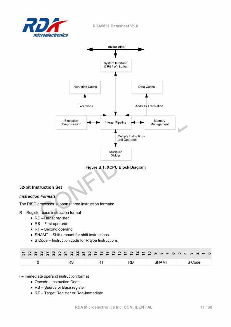
B.I.1 System CPU (XCPU)The XCPU RISC is a 16/32-bits processor. Using a Reduced Instruction Set Architecture, an efficient 6-stage instruction pipeline and separated Instruction and Data caches, it provides high performance to the system. The Pipeline Stages are as follows:
● PC. Program Counter. Calculate the address of the next instruction and send it to the instruction cache.● IF. Instruction Fetch. In this stage the instruction cache is being accessed and the instruction
information is retrieved.● RF. Register File. The register file is being accessed and the instruction is decoded.● EX. Execution. The instruction is executed● DC. Data Memory read and write access.● WB. Write Back. Results are written back to the register file.
Features
● RDA RISC Core.○ 32x32-bit Multiplier.○ 32x32-bit -> 64-bit Multiplier Accumulator (MAC) in 2 cycles (pipelined).○ Read / Write Buffer.○ 16/32 bit instruction set.
● 32 interrupt sources.● 4 kByte Instruction Cache.● 4 kByte Data Cache.● 16 byte streaming buffer to accelerate uncached instruction accesses.
Block Diagram
RDA Microelectronics Inc. CONFIDENTIAL 10 / 88
RDA5851 Datasheet V1.0
32-bit Instruction Set
Instruction Formats
The RISC processor supports three instruction formats:
R – Register base instruction format● RD –Target register ● RS – First operand ● RT – Second operand ● SHAMT – Shift amount for shift instructions ● S Code – Instruction code for R type Instructions
31 30 29 28 27 26 25 24 23 22 21 20 19 18 17 16 15 14 13 12 11 10 9 8 7 6 5 4 3 2 1 0
0 RS RT RD SHAMT S Code
I – Immediate operand instruction format● Opcode –Instruction Code ● RS – Source or Base register ● RT – Target Register or Reg-Immediate
RDA Microelectronics Inc. CONFIDENTIAL 11 / 88
Figure B.1: XCPU Block Diagram
System Interface& Rd / Wr Buffer
System Interface& Rd / Wr Buffer
Instruction CacheInstruction Cache Data CacheData Cache
Integer PipelineInteger Pipeline
AMBA AHB
MemoryManagement
MemoryManagement
ExceptionCo-processorException
Co-processor
MultiplierDivider
MultiplierDivider
Multiply Instructionsand Operands
Address TranslationExceptions
RDA5851 Datasheet V1.0
● Immediate – 16 bit Immediate or Displacement
31 30 29 28 27 26 25 24 23 22 21 20 19 18 17 16 15 14 13 12 11 10 9 8 7 6 5 4 3 2 1 0
Opcode RS RT Immediate
J – Jump instruction format● Opcode –Instruction Code ● Jump Immediate – Immediate 26 bit for jump instruction address
31 30 29 28 27 26 25 24 23 22 21 20 19 18 17 16 15 14 13 12 11 10 9 8 7 6 5 4 3 2 1 0
Opcode Jump Immediate
Supported Instructions
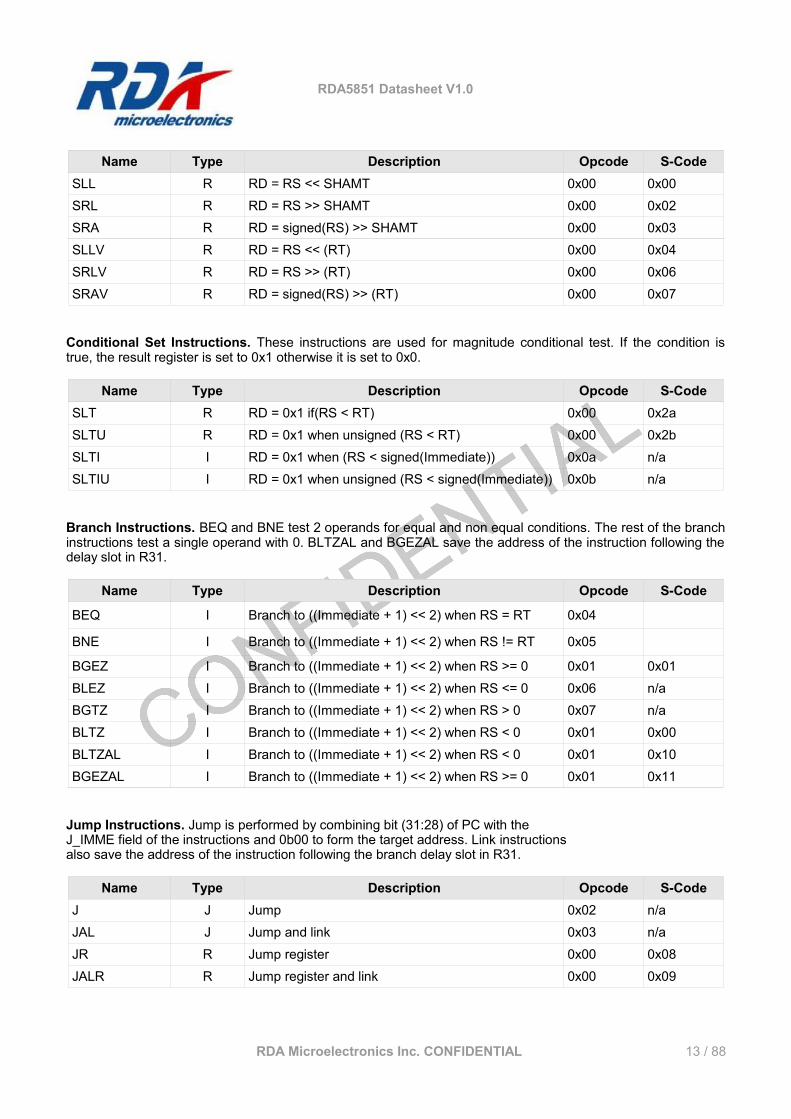
Arithmetic Instructions.
Name Type Description Opcode S-CodeADD R RD = RS + RT 0x00 0x20ADDU R Unsigned[RD = RS + RT] 0x00 0x21SUB R RD = RS – RT 0x00 0x22SUBU R Unsigned[ RD = RS – RT] 0x00 0x23ADDI I RT = RS + Signed(Immediate) 0x08 n/aADDIU I RT = RS + Unsigned(Immediate) 0x09 n/a
Logical Instructions. Logical instructions are all bit wise operations.
Name Type Description Opcode S-CodeAND R RD = RS and RT 0x00 0x24OR R RD = RS or RT 0x00 0x25XOR R RD = RS xor RT 0x00 0x26NOR R RD = not(RS or RT) 0x00 0x27ANDI I RT = RS and Zero-extend(Immediate) 0x0c n/aORI I RT = RS or Zero-extend(Immediate) 0x0d n/aXORI I RT = RS xor Zero-extend(Immediate) 0x0e n/a
Shift Instructions.
RDA Microelectronics Inc. CONFIDENTIAL 12 / 88
RDA5851 Datasheet V1.0
Name Type Description Opcode S-CodeSLL R RD = RS << SHAMT 0x00 0x00SRL R RD = RS >> SHAMT 0x00 0x02SRA R RD = signed(RS) >> SHAMT 0x00 0x03SLLV R RD = RS << (RT) 0x00 0x04SRLV R RD = RS >> (RT) 0x00 0x06SRAV R RD = signed(RS) >> (RT) 0x00 0x07
Conditional Set Instructions. These instructions are used for magnitude conditional test. If the condition is true, the result register is set to 0x1 otherwise it is set to 0x0.
Name Type Description Opcode S-CodeSLT R RD = 0x1 if(RS < RT) 0x00 0x2aSLTU R RD = 0x1 when unsigned (RS < RT) 0x00 0x2bSLTI I RD = 0x1 when (RS < signed(Immediate)) 0x0a n/aSLTIU I RD = 0x1 when unsigned (RS < signed(Immediate)) 0x0b n/a
Branch Instructions. BEQ and BNE test 2 operands for equal and non equal conditions. The rest of the branch instructions test a single operand with 0. BLTZAL and BGEZAL save the address of the instruction following the delay slot in R31.
Name Type Description Opcode S-Code
BEQ I Branch to ((Immediate + 1) << 2) when RS = RT 0x04 BNE I Branch to ((Immediate + 1) << 2) when RS != RT 0x05 BGEZ I Branch to ((Immediate + 1) << 2) when RS >= 0 0x01 0x01BLEZ I Branch to ((Immediate + 1) << 2) when RS <= 0 0x06 n/aBGTZ I Branch to ((Immediate + 1) << 2) when RS > 0 0x07 n/aBLTZ I Branch to ((Immediate + 1) << 2) when RS < 0 0x01 0x00BLTZAL I Branch to ((Immediate + 1) << 2) when RS < 0 0x01 0x10BGEZAL I Branch to ((Immediate + 1) << 2) when RS >= 0 0x01 0x11
Jump Instructions. Jump is performed by combining bit (31:28) of PC with theJ_IMME field of the instructions and 0b00 to form the target address. Link instructionsalso save the address of the instruction following the branch delay slot in R31.
Name Type Description Opcode S-CodeJ J Jump 0x02 n/aJAL J Jump and link 0x03 n/aJR R Jump register 0x00 0x08JALR R Jump register and link 0x00 0x09
RDA Microelectronics Inc. CONFIDENTIAL 13 / 88
RDA5851 Datasheet V1.0
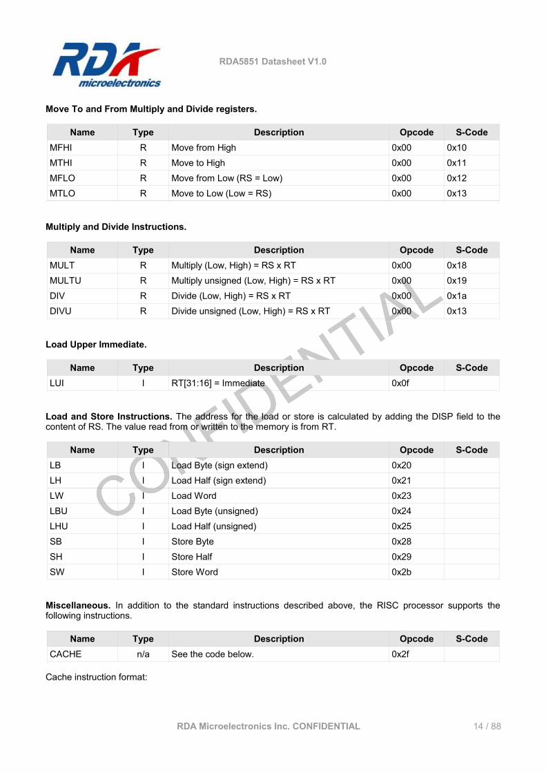
Move To and From Multiply and Divide registers.
Name Type Description Opcode S-CodeMFHI R Move from High 0x00 0x10MTHI R Move to High 0x00 0x11MFLO R Move from Low (RS = Low) 0x00 0x12MTLO R Move to Low (Low = RS) 0x00 0x13
Multiply and Divide Instructions.
Name Type Description Opcode S-CodeMULT R Multiply (Low, High) = RS x RT 0x00 0x18MULTU R Multiply unsigned (Low, High) = RS x RT 0x00 0x19DIV R Divide (Low, High) = RS x RT 0x00 0x1aDIVU R Divide unsigned (Low, High) = RS x RT 0x00 0x13
Load Upper Immediate.
Name Type Description Opcode S-CodeLUI I RT[31:16] = Immediate 0x0f
Load and Store Instructions. The address for the load or store is calculated by adding the DISP field to the content of RS. The value read from or written to the memory is from RT.
Name Type Description Opcode S-CodeLB I Load Byte (sign extend) 0x20LH I Load Half (sign extend) 0x21LW I Load Word 0x23LBU I Load Byte (unsigned) 0x24LHU I Load Half (unsigned) 0x25SB I Store Byte 0x28SH I Store Half 0x29SW I Store Word 0x2b
Miscellaneous. In addition to the standard instructions described above, the RISC processor supports the following instructions.
Name Type Description Opcode S-CodeCACHE n/a See the code below. 0x2f
Cache instruction format:
RDA Microelectronics Inc. CONFIDENTIAL 14 / 88
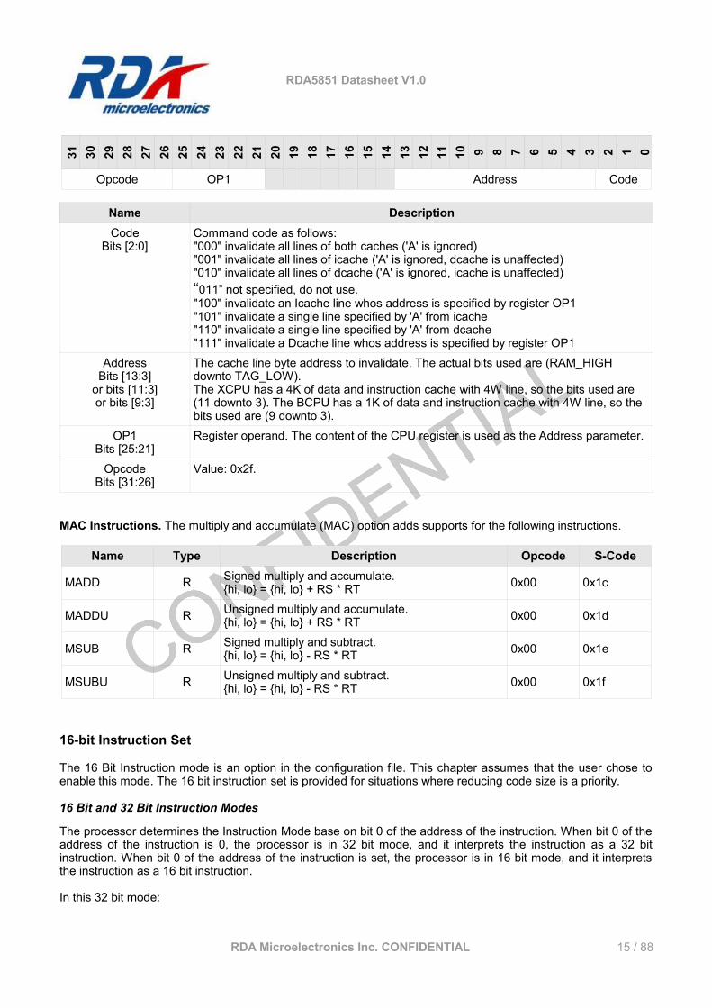
RDA5851 Datasheet V1.031 30 29 28 27 26 25 24 23 22 21 20 19 18 17 16 15 14 13 12 11 10 9 8 7 6 5 4 3 2 1 0
Opcode OP1 Address Code
Name DescriptionCode
Bits [2:0]Command code as follows:"000" invalidate all lines of both caches ('A' is ignored)"001" invalidate all lines of icache ('A' is ignored, dcache is unaffected)"010" invalidate all lines of dcache ('A' is ignored, icache is unaffected)“011” not specified, do not use."100" invalidate an Icache line whos address is specified by register OP1"101" invalidate a single line specified by 'A' from icache"110" invalidate a single line specified by 'A' from dcache"111" invalidate a Dcache line whos address is specified by register OP1
AddressBits [13:3]
or bits [11:3]or bits [9:3]
The cache line byte address to invalidate. The actual bits used are (RAM_HIGH downto TAG_LOW).The XCPU has a 4K of data and instruction cache with 4W line, so the bits used are (11 downto 3). The BCPU has a 1K of data and instruction cache with 4W line, so the bits used are (9 downto 3).
OP1Bits [25:21]
Register operand. The content of the CPU register is used as the Address parameter.
OpcodeBits [31:26]
Value: 0x2f.
MAC Instructions. The multiply and accumulate (MAC) option adds supports for the following instructions.
Name Type Description Opcode S-Code
MADD R Signed multiply and accumulate.{hi, lo} = {hi, lo} + RS * RT 0x00 0x1c
MADDU R Unsigned multiply and accumulate.{hi, lo} = {hi, lo} + RS * RT 0x00 0x1d
MSUB R Signed multiply and subtract.{hi, lo} = {hi, lo} - RS * RT 0x00 0x1e
MSUBU R Unsigned multiply and subtract.{hi, lo} = {hi, lo} - RS * RT 0x00 0x1f
16-bit Instruction Set
The 16 Bit Instruction mode is an option in the configuration file. This chapter assumes that the user chose to enable this mode. The 16 bit instruction set is provided for situations where reducing code size is a priority.
16 Bit and 32 Bit Instruction Modes
The processor determines the Instruction Mode base on bit 0 of the address of the instruction. When bit 0 of the address of the instruction is 0, the processor is in 32 bit mode, and it interprets the instruction as a 32 bit instruction. When bit 0 of the address of the instruction is set, the processor is in 16 bit mode, and it interprets the instruction as a 16 bit instruction.
In this 32 bit mode:
RDA Microelectronics Inc. CONFIDENTIAL 15 / 88
RDA5851 Datasheet V1.0
1. The instruction counter is incremented by 4 from 1 instruction to the next.2. For Branch and Link instructions, the processor save the address of the instruction + 8 as the return address. This is the instruction after the delay slot.3. The processor will take an Illegal Instruction Exception, if either bit 0 or bit 1 are set.
In this 16 bit mode:
1. The instruction counter is incremented by 2 from 1 instruction to the next.2. For Branch and Link instructions, the processor save the address of the instruction + 4 as the return address. This is the instruction after the delay slot.3. The processor passes bit 1 of the instruction address to the memory subsystem.Bit 0 is always sent as 0 to the memory subsystem.
Switching between 32 Bit and 16 Bit modes.
To switch between the modes, bit 0 of the instruction address must be changed from 1 to 0 and back. There are 2 basic mechanisms to achieve this.
JALX instruction. This instruction exists in both 32 bit and 16 bit modes. In addition to changing the execution path to the target address, it also toggles bit 0 of the instruction and hence the mode.
JR, JALR instructions. These instructions take the 32 bit contents of a register and use it as the target address. Bit 0 of the register can be set to reflect the mode of the instructions at the target address.
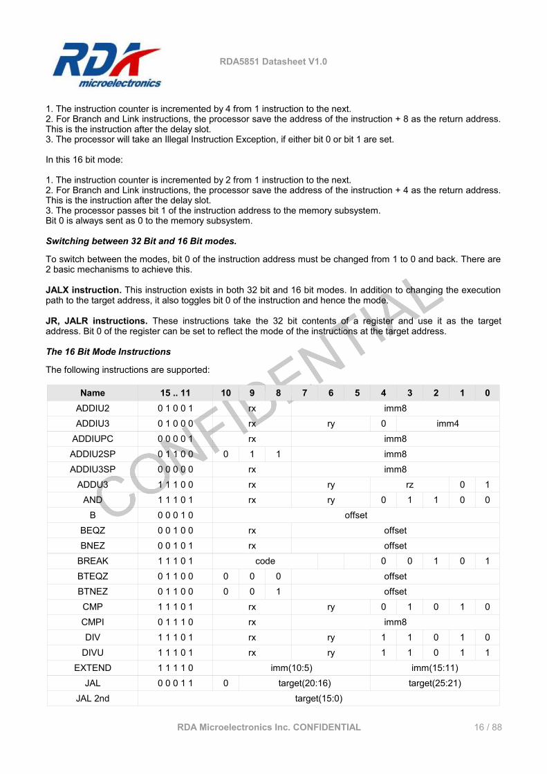
The 16 Bit Mode Instructions
The following instructions are supported:
Name 15 .. 11 10 9 8 7 6 5 4 3 2 1 0ADDIU2 0 1 0 0 1 rx imm8ADDIU3 0 1 0 0 0 rx ry 0 imm4
ADDIUPC 0 0 0 0 1 rx imm8ADDIU2SP 0 1 1 0 0 0 1 1 imm8ADDIU3SP 0 0 0 0 0 rx imm8
ADDU3 1 1 1 0 0 rx ry rz 0 1AND 1 1 1 0 1 rx ry 0 1 1 0 0
B 0 0 0 1 0 offsetBEQZ 0 0 1 0 0 rx offsetBNEZ 0 0 1 0 1 rx offset
BREAK 1 1 1 0 1 code 0 0 1 0 1BTEQZ 0 1 1 0 0 0 0 0 offsetBTNEZ 0 1 1 0 0 0 0 1 offsetCMP 1 1 1 0 1 rx ry 0 1 0 1 0CMPI 0 1 1 1 0 rx imm8DIV 1 1 1 0 1 rx ry 1 1 0 1 0
DIVU 1 1 1 0 1 rx ry 1 1 0 1 1EXTEND 1 1 1 1 0 imm(10:5) imm(15:11)
JAL 0 0 0 1 1 0 target(20:16) target(25:21)JAL 2nd target(15:0)
RDA Microelectronics Inc. CONFIDENTIAL 16 / 88
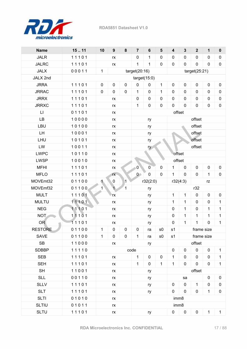
RDA5851 Datasheet V1.0
Name 15 .. 11 10 9 8 7 6 5 4 3 2 1 0JALR 1 1 1 0 1 rx 0 1 0 0 0 0 0 0
JALRC 1 1 1 0 1 rx 1 1 0 0 0 0 0 0JALX 0 0 0 1 1 1 target(20:16) target(25:21)
JALX 2nd target(15:0)JRRA 1 1 1 0 1 0 0 0 0 0 1 0 0 0 0 0
JRRAC 1 1 1 0 1 0 0 0 1 0 1 0 0 0 0 0JRRX 1 1 1 0 1 rx 0 0 0 0 0 0 0 0
JRRXC 1 1 1 0 1 rx 1 0 0 0 0 0 0 0LI 0 1 1 0 1 rx offsetLB 1 0 0 0 0 rx ry offset
LBU 1 0 1 0 0 rx ry offsetLH 1 0 0 0 1 rx ry offset
LHU 1 0 1 0 1 rx ry offsetLW 1 0 0 1 1 rx ry offset
LWPC 1 0 1 1 0 rx offsetLWSP 1 0 0 1 0 rx offsetMFHI 1 1 1 0 1 rx 0 0 0 1 0 0 0 0MFLO 1 1 1 0 1 rx 0 0 0 1 0 0 1 0
MOVEmt32 0 1 1 0 0 1 0 1 r32(2:0) r32(4:3) rzMOVEmf32 0 1 1 0 0 1 1 1 ry r32
MULT 1 1 1 0 1 rx ry 1 1 0 0 0MULTU 1 1 1 0 1 rx ry 1 1 0 0 1
NEG 1 1 1 0 1 rx ry 0 1 0 1 1NOT 1 1 1 0 1 rx ry 0 1 1 1 1OR 1 1 1 0 1 rx ry 0 1 1 0 1
RESTORE 0 1 1 0 0 1 0 0 0 ra s0 s1 frame sizeSAVE 0 1 1 0 0 1 0 0 1 ra s0 s1 frame size
SB 1 1 0 0 0 rx ry offsetSDBBP 1 1 1 1 0 code 0 0 0 0 1
SEB 1 1 1 0 1 rx 1 0 0 1 0 0 0 1SEH 1 1 1 0 1 rx 1 0 1 1 0 0 0 1SH 1 1 0 0 1 rx ry offsetSLL 0 0 1 1 0 rx ry sa 0 0
SLLV 1 1 1 0 1 rx ry 0 0 1 0 0SLT 1 1 1 0 1 rx ry 0 0 0 1 0SLTI 0 1 0 1 0 rx imm8
SLTIU 0 1 0 1 1 rx imm8SLTU 1 1 1 0 1 rx ry 0 0 0 1 1
RDA Microelectronics Inc. CONFIDENTIAL 17 / 88
RDA5851 Datasheet V1.0
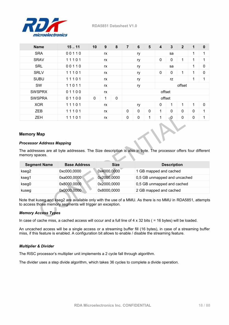
Name 15 .. 11 10 9 8 7 6 5 4 3 2 1 0SRA 0 0 1 1 0 rx ry sa 1 1
SRAV 1 1 1 0 1 rx ry 0 0 1 1 1SRL 0 0 1 1 0 rx ry sa 1 0
SRLV 1 1 1 0 1 rx ry 0 0 1 1 0SUBU 1 1 1 0 1 rx ry rz 1 1SW 1 1 0 1 1 rx ry offset
SWSPRX 0 1 1 0 0 rx offsetSWSPRA 0 1 1 0 0 0 1 0 offset
XOR 1 1 1 0 1 rx ry 0 1 1 1 0ZEB 1 1 1 0 1 rx 0 0 0 1 0 0 0 1ZEH 1 1 1 0 1 rx 0 0 1 1 0 0 0 1
Memory Map
Processor Address Mapping
The addresses are all byte addresses. The Size description is also in byte. The processor offers four different memory spaces.
Segment Name Base Address Size Descriptionkseg2 0xc000,0000 0x4000,0000 1 GB mapped and cachedkseg1 0xa000,0000 0x2000,0000 0,5 GB unmapped and uncachedkseg0 0x8000,0000 0x2000,0000 0,5 GB unmapped and cachedkuseg 0x0000,0000 0x8000,0000 2 GB mapped and cached
Note that kuseg and kseg2 are available only with the use of a MMU. As there is no MMU in RDA5851, attempts to access those memory segments will trigger an exception.
Memory Access Types
In case of cache miss, a cached access will occur and a full line of 4 x 32 bits ( = 16 bytes) will be loaded.
An uncached access will be a single access or a streaming buffer fill (16 bytes), in case of a streaming buffer miss, if this feature is enabled. A configuration bit allows to enable / disable the streaming feature.
Multiplier & Divider
The RISC processor’s multiplier unit implements a 2 cycle fall through algorithm.
The divider uses a step divide algorithm, which takes 36 cycles to complete a divide operation.
RDA Microelectronics Inc. CONFIDENTIAL 18 / 88
RDA5851 Datasheet V1.0
B.I.2 Memory BridgeThe memory bridge is the interface to general memory used by the system, including internal rom, internal sram and access to external memory.
Features
● Dual AHB Slave○ A rom/sram controller○ An Asynchronous FIFO to external controller
● The bridge is implemented as a crossbar between the 2 AHB and the 2 controller (rom/sram and FIFO)● The rom/sram controller can insert wait cycle to the AHB Slave (to manage read/write conflicts and to
allow using slower instance if needed).● The rom/sram controller integrate a BIST engine to test the ROM by computing a CRC and test the
rams with the March C algorithm● All AHB burst size are supported
○ Wrap will be split at wrap address○ Burst longer than the data buffer size of the FIFO will be split○ Read INCR will read a fixed data size
● FIFO data buffer can store 2 requests either read or write (each 4x32 bytes) from either AHB slave interface.
● APB slave for configuration
External Bus Controller Features
● The controller handles 16 bits data bus width only, however 8 bit memory chips can still be used; by groups of 2. 8 bit peripherals must be connected to the 8 LSBs of data and accessed through even addresses only.
● Manage page mode SRAM or FLASH.● Manage burst mode PseudoSRAM.● Manage AD-Mux and AD-Mux burst mode PseudoSRAM.● 1 Control Register Enable (M_CRE) Output pin in same power domain than other memory IO for
PseudoSRAM register control.● FIFO interface for address/data path● APB interface for configuration (subset of the mem bridge APB address space)
AHB Master Features
● AHB Compliant master● except the 1K crossing limit defined by AMBA (additional logic required)● Memory space divided in 5 spaces with a base address for each (aligned on n Word address, n=FIFO
data buffer size)● Do not use WRAP (due to FIFO organization) ● use INCR4, SINGLE or INCR (for 2 or 3 data only) burst type● FIFO interface for address/data path● APB interface for configuration (subset of the mem bridge APB address space)● External clock is provided from outside the IP (and synthesized in the outside clock tree)
RDA Microelectronics Inc. CONFIDENTIAL 19 / 88
RDA5851 Datasheet V1.0
Operations
Dual AHB Operation
The Slave allow simultaneous access to rom/sram controller and FIFO from the two slaves.Access to the rom/sram controller are sequenced using WAIT on AHB (HReady low).Access to the FIFO are sequenced using split when the FIFO busy on the other AHB slave (other split conditions are described bellow in FIFO Operation section).
Arbitration in case of simultaneous access to the same controller: Should try to serve each side (BB and Sys) alternatively.Simultaneous access to rom/sram controller: memorize the last accepted burst. when the two arrives exactly simultaneously reply wait to the memorized side and process the other side.Simultaneous access to FIFO: First serve read of data if data are available for this read. Serve the side that did not enter the FIFO on last Burst in priority.
FIFO Operation
The FIFO can store 2 requests either read or write from either AHB Slave interface. But only one at a time.For each request there is an associated Write Data Buffer and a Read Data Buffer.
If the FIFO is full the master is split, this master will be released when one spot is free in the FIFO (all masters split because FIFO was full are released at the same time).
WriteA burst is stored to the Data buffer until the burst is finished. If the Data buffer is full or the Wrap address of a wrap burst is reached, the Split response is send (the master will be released in the same condition as above).
ReadThe request is stored (address, length ...) and the master is split.The master will be released when the Data buffer has been filled by the external controller (EBC or AHB Master). When the Master comes back, the Data are provided, if the master end the burst the transfer is complete (even if there is still some data in the buffer, in this case they are lost) if the master request more than the available Data it receive the Split response and will be released in the same conditions as for FIFO full: the request is not stored.
FIFO Flush status: Read in FIFO at special address space does not impact the external controller but returns when the command has reached the end of the FIFO (so the read returns only when previous writes are done, no pooling is required)
If external controller has error (disabled space for EBC or AHB Error response for master) the FIFO data reads as and error code. “0xD15AB1ED”
EBC Operation
FIFO access are translated to external memory access.
Configuration of Chip select are validated only between access (atomic change)
● Flash block address remapping and M_CRE control registers are placed in the FIFO space to keep accesses in sequence and avoid using FIFO Flush each time.
RDA Microelectronics Inc. CONFIDENTIAL 20 / 88
RDA5851 Datasheet V1.0
B.I.3 Direct Memory Access (DMA)The DMA controller relieve the CPU from doing generic memory transfers. A data FIFO is integrated to allow burst transfers. It can generate an interrupt to the system CPU at transfer completion.
Read and Write transfers are supported from and to any memory mapped location (external memory, internal SRAM, modules FIFO…). The addresses can be word, halfword or byte aligned. The DMA can also be used in pattern mode. In this case, a 32-bit word will be used to fill the destination memory zone.
Features
● Support for linear memory transfers.● Support for word, halfword and byte aligned addresses.● Burst transfer mode and internal FIFO for best performances.● Autonomous transfer up to 64K byte per transfer.● Interrupt generation at completion of the transaction.● Can fill a part of the memory with a 32-bit pattern.
B.I.4 Page SpyThis module is a System spy that detects read or write access into predefined ranges of memory addresses and triggers an interrupt in case of selected access.
Features
● Six memory spaces can be spied.● Memory space described with a start address (inclusive) and an end address (exclusive) and mode
(detect read, write or both).● For each space a status register gives the master that triggered the spy, the address that caused it and
the mode.
B.I.5 System Intelligent Flow Controller (Sys IFC)The System Intelligent Flow Controller (SYS_IFC) is a bridge between the system bus and the peripheral bus. The IFC also provides DMA capabilities to allow data transfer from or to peripherals. It supports 7 DMA standard channels for 8-bit or 32-bit and a dedicated DMA channel for the RF SPI module.
Features
● 7 independent DMA channels. internal FIFO of four 32-bit words per channel.● 1 dedicated DMA channel for the debug host● Burst mode on AHB bus to enhance transfer rate● Support 2 types of transfer: memory to peripheral and peripheral to memory● Incremental address for AHB master access and non-incremental address for APB access.● Dynamic allocation of the 7 DMA channels, request lines among the following peripherals:
a) SCI
RDA Microelectronics Inc. CONFIDENTIAL 21 / 88
RDA5851 Datasheet V1.0
b) SPI1c) SPI2d) SPI3e) TRACE UART (DBG Host)f) UARTg) UART2h) SDMMCi) Camera
● Hardware semaphore registers which indicate to the CPU which channel must be used and a global status register indicating which channel is free.
● AHB to APB bridge, write buffer for a single write access the master isn't stalled, no wait state inserted
AHB2APB bridge operationThe SYS_IFC include a bridge between the AHB bus and the APB bus. The SYS_IFC bus is the only one master on the APB bus. The APB bus is a low bandwidth and low power bus mainly used to configure peripheral register or transfer data with the IFC DMA.
Arbitration
The IFC includes some DMA capability which can access to APB bus, in case of 2 accesses simultaneously (AHB slave and DMA channel), request from the AHB has the highest priority. But if processor requests an access to the APB, and the DMA already have an access in progress, the processor will be stalled until the DMA access is finished.
DMA OperationsThe SYS IFC includes 7 DMA channels. Each channel can perform data movements between devices in the AHB bus and peripheral on the APB bus.
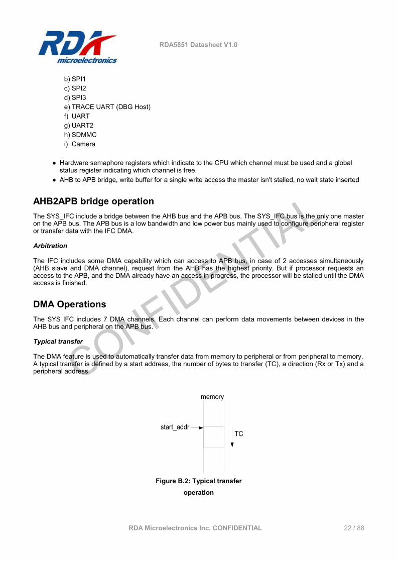
Typical transfer
The DMA feature is used to automatically transfer data from memory to peripheral or from peripheral to memory.A typical transfer is defined by a start address, the number of bytes to transfer (TC), a direction (Rx or Tx) and a peripheral address.
RDA Microelectronics Inc. CONFIDENTIAL 22 / 88
Figure B.2: Typical transfer operation
start_addr
memory
TC
RDA5851 Datasheet V1.0
START_ADDR register gives the first address of the data to transfer.
TC register gives the number of bytes to transfer.
The direction and the peripheral to access is given by the field REQ_SRC in the control register.
Typical data flow for memory to peripheral transfer
1. Check which channel to use and which channel is busy.2. Configure in the given channel of the IFC, the AHB start address.3. Configure in the given channel of the IFC, the number of bytes to transfer (TC register)4. Program the peripheral in which to write and enable the IFC channel to start.5. The IFC start a read burst access on its AHB master interface.6. If the programmable DMA request line (of the peripheral associated to this transfer) is high (meaning the7. peripheral needs data), writes are performed on the APB interface and the current transfer counter (TC)
is decremented. This sequence is made until the FIFO of the IFC is empty.8. When the FIFO of the IFC is empty; another read burst access is performed on the AHB bus and return
to the step (6).9. If the transfer is complete (current transfer counter reaches zero), the associated Done signals goes
high and the channel is disabled (if the autodisable bit is set)
This is the same flow for peripheral to memory transfer.
Auto-disable bit
At the end of the transfer when TC=0 the channel is not necessary disabled. The state of the autodisable bit determines whether or not the channel is automatically disabled. This allows for one resource to keep the channel, and this resource can launch a new transfer just by writing a new value to the TC.
Incremental TC
It is possible during the transfer to write several time in the TC register. The new TC value will be added to the current value of the TC and the total number of bytes transferred is a the addition of all writes in TC. For example, at first the processor programs the IFC with TC=50, and the IFC start the transfer. Later during the transfer the processor again writes TC=30. The total number of transfers will be 80 bytes whichis 80=50+30.
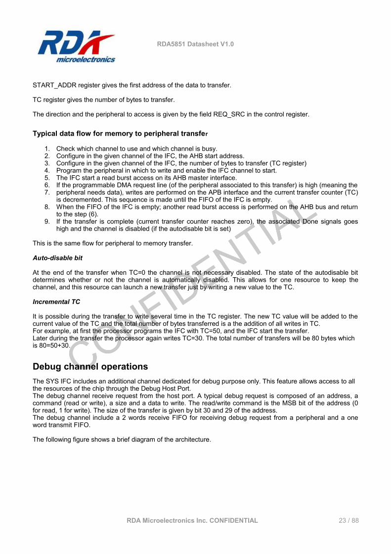
Debug channel operationsThe SYS IFC includes an additional channel dedicated for debug purpose only. This feature allows access to allthe resources of the chip through the Debug Host Port.The debug channel receive request from the host port. A typical debug request is composed of an address, a command (read or write), a size and a data to write. The read/write command is the MSB bit of the address (0 for read, 1 for write). The size of the transfer is given by bit 30 and 29 of the address.The debug channel include a 2 words receive FIFO for receiving debug request from a peripheral and a one word transmit FIFO.
The following figure shows a brief diagram of the architecture.
RDA Microelectronics Inc. CONFIDENTIAL 23 / 88
RDA5851 Datasheet V1.0
For a write debug command, the host peripheral transmits by a first DMA request the Address, the R/W bit and the Size and by a second DMA request the DATA to write. Then the debug channel makes an AHB write access to desired resource.
For a read debug command, the host peripheral transmits by a first DMA request the Address, the R/W bit and the Size and by a second DMA request a data to only fill the internal debug command FIFO. The data loaded in the FIFO during this second access is not used. With the address loaded, the IFC performs an AHB read access, the recovered data is stored in the transmit FIFO. When the host peripheral performs a DMA transmit request, a write access is performed on the APB bus for sending data to the peripheral.
B.II System Peripherals
B.II.1 System and Clock ControlThe system control provides general controls over the whole system, including reset controls, power management controls, clock selection, and some debug features.
Features
● Registers for reset control, clock control, fast clock div control, AHBC, some debug feature(like Debug Breakpoints,Lock / Unlock the protected registers),.
● Automatic clock gating signal generation for APB module (PCLK_DATA and PCLK_CONF)● XCPU and CPU special signals for clock management and breakpoint management
Reset Control
After a hardware reset, the XCPU will automatically boot and perform the system initialization. The CPU is held in reset until released by the XCPU.
RDA Microelectronics Inc. CONFIDENTIAL 24 / 88
Figure B.3: Debug channel block diagram
DebugChannel
data to write
Address + R/W
Peripheral
AHBmaster
read data
RDA5851 Datasheet V1.0
The reset control allows resetting independently most of the modules of the design. In normal use, there should be no need to reset an individual module and caution must be taken when doing so to avoid crashing the system. This is provided mainly for debug purposes.
A global software reset feature is provided. This feature allows resetting the whole system from the software running on any of the CPUs. The effect of the software reset is the same as a hardware reset except that it does not reset the host interface.
A watchdog timer allows recovering from software crashes. Once enabled, the watchdog timer must be reloaded periodically by the software. If the software fails to do so because of a software crash, the watchdog timer will reach 0 and trigger a software reset automatically. The system will then restart. When the XCPU reboots, it can detect that a watchdog has triggered a reset and can save the context at the time of the watchdog expiration(Program counter, register values, stack location), this should allow for easier software debug.
It is also possible to trigger a software reset from the host interface. A special feature allows preventing the XCPU from booting after this reset. This allows avoiding the XCPU to set the system in an invalid configuration in case the boot code is not valid (flash not programmed or badly programmed) and gaining access to the whole system from the host port to find the cause of the issue or reprogram the boot code in flash.
Clock management
The system has three main sources for the internal clocks generation:● a 32.768kHz generated by 26MHz clock● a 26MHz clock from the RF transceiver ● a PLL that generates 624MHz from 26MHz provided by the clock Squarer, this PLL allows to generate a
26MHz, 39MHz, 52MHz, 78MHz, 89MHz, 104MHz, 113MHz, 125MHz, 139MHz, 156MHz, 178MHz, 208MHz, 250MHz, 312MHz;
The other clock source can go only to some part of the design:● a dedicated clock input for the HST clock : used by the host module.● an audio clock input (BCK) : used for the I2S audio module, note that this pin is actually bidirectional
(depending on the connection to a I2S master or I2S slave, this pin is configured as a clock input i_BCK or a clock output o_BCK).
All internal clocks in the design except the clocks for host and in some case audio, derive from one of the three main clock sources. The selection is made through configuration registers. Thanks to glitch free muxes, it is possible to change the internal clock frequency on the fly. Caution must be taken when changing the main clock frequency as some interfaces clocks are divided versions of this main clock. For example, the SPI baud rate directly depends on the main clock frequency so when changing the main clock, it is recommended to make sure that the SPI is not transmitting during the change.
To reduce the power consumption, it is possible to gate the clock signal going to most of the modules individually when a module is not in use. Enabling or disabling the clock going to a module can be automatic (all the modules needing to run over short period of times are able to control their clock themselves. For example the DMA only has a clock while doing a transfer) or manual (for the modules running all the time once they are enabled. For example, the audio interface which needs to output samples continuously once enabled)
Debug features
Hardware breakpoints
This feature allows defining one hardware breakpoint for each CPU. This breakpoint can be either on an instruction fetch, a data read or a data write.
RDA Microelectronics Inc. CONFIDENTIAL 25 / 88
RDA5851 Datasheet V1.0
When the breakpoint is reached, the CPU is stalled. A status bit allows to know if the breakpoint has been reached or not. When the CPU is stalled, all its internal registers are accessible through the host port. If the breakpoint is released, the CPU resumes its execution.
Debug clock
It is possible to output any internal clock of the design on the pin DBG_CLK (also used for EXL/PXTS Clock) for debug purposes (check frequency, power saving feature...). The Debug clock register is defined in the debug_port module.
B.II.2 Trace (Normal UART) and Host (Debug UART) Port
RDA5851 Debug Host module contains 1 normal Universal Asynchronous Receiver Transmitter channels (UART) and 1 Debug UART. The two UARTs share the same Tx/Rx engines, which sends and receives byte data from serial interface. Each UART has its own control sub-module and own APB interface. RDA5851 Debug Host module parses the incoming data from serial interface to switch between the normal UART and the Debug UART.
● Normal UARTThe normal UART can be used for traces and other purposes. For APB interface, it is exactly the same to the other UARTs in the RDA5851 system. However, if Debug UART is enabled, it should have the same serial interface configuration as the Debug UART. Some of its configuration options will be masked in this case. To Adapt different clock frequency, the normal UART uses asynchronous FIFO, which uses gray code to represent the read and write pointer positions.
● Debug UARTThe Debug UART is specially designed for communicating debug information with a PC host. The serial interface of Debug UART is a simplified version of the normal UART and is less configurable. Each sample is sent serially, has 1 start bit (always zero), 8 data bits, and 1 stop bits (always one). Breaks (data line held low) can be generated and detected allowing resynchronizing the two devices.
Features
● Auto normal/Debug UART select by parsing incoming message.● Separate UART APB and Debug UART APB interfaces.
Normal UART features:● Fully programmable transfer word format.
○ 7 or 8 data bits.○ 1 or 2 stop bits.○ Odd, even, mark, space or none parity.
● Smooth stop feature (the UART stops after the end of the current word transfer).● Break generation and detection.
○ Break length programmable.○ Interrupt can be generated.
● Supports Automatic Software Flow Control (XON/XOFF).● Programmable receive and transmit fifos (16 bytes deep).● Supports low speed IrDA 1.0 SIR mode by adding external hardware.● DMA capabilities (through the System IFC) to allow fully automated data transfers.
RDA Microelectronics Inc. CONFIDENTIAL 26 / 88
RDA5851 Datasheet V1.0
● Wide selection of programmable interrupts to allow interrupt driven data transfer management.○ Rx or Tx Fifo trigger reached.○ Timeout: No characters in or out of the Rx Fifo during the last 4 character times and there is at
least one character in the Rx Fifo during this time.○ DMA timeout: After Rx Sys IFC DMA is started, no characters in or out of the Rx Fifo during the
last 4 character times.○ End of the Sys IFC DMA transfer.○ CTS detection.○ Tx or Rx overflow, parity or framing (bad sample format received) error or break.
● Loop Back capabilities for test purposes.● Up to 1843.2 Kbit/s for serial and 115.2 Kbit/s for IrDA.
Debug UART features: ● Transfer word format.
○ 1 start bit.○ 8 data bits.○ 1 stop bit.
● Tx Break generation when pin reset and Rx break detection.● HW reset event.● Programmable events allowing CPU directly write to Debug UART.● Some serial interface read/write internal registers.● DMA capabilities (through the System IFC Debug Channel) for automated data transfers.● Up to 1843.2 Kbit/s for serial.
Message Frame
In case of Debug UART is disabled, the message has no format requirement. If Debug UART is enabled, the General message received by the Debug Host should be of the following format:
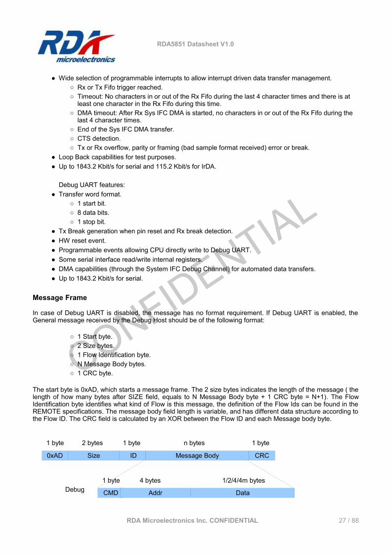
○ 1 Start byte.○ 2 Size bytes. ○ 1 Flow Identification byte.○ N Message Body bytes.○ 1 CRC byte.
The start byte is 0xAD, which starts a message frame. The 2 size bytes indicates the length of the message ( the length of how many bytes after SIZE field, equals to N Message Body byte + 1 CRC byte = N+1). The Flow Identification byte identifies what kind of Flow is this message, the definition of the Flow Ids can be found in the REMOTE specifications. The message body field length is variable, and has different data structure according to the Flow ID. The CRC field is calculated by an XOR between the Flow ID and each Message body byte.
RDA Microelectronics Inc. CONFIDENTIAL 27 / 88
0xAD Message Body IDSize CRC
1 byte 2 bytes 1 byte n bytes 1 byte
CMD Addr Data
1 byte 4 bytes 1/2/4/4m bytes Debug
RDA5851 Datasheet V1.0
Figure B.4: General Message Format
For Debug Messages, the Flow_ID = 255, and the Message Body field is composed of:
○ 1 command byte ( bit 7,bits 2 to 0 used).○ x00 for byte.○ x01 for half word.○ x10 for word.○ x11 for block.○ 1xx for internal registers.○ Bit 7 for Write_H (0 for read, 1 for write)○ 4 address bytes (bits 28 to 0 used). ○ Byte, half word, word or 4m data bytes(block) in case of write, 1 data byte in case of read (RID).
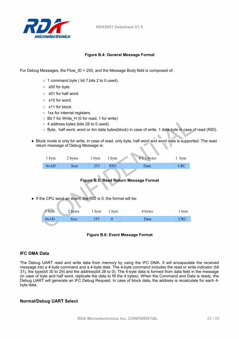
● Block mode is only for write, in case of read, only byte, half word and word data is supported. The read return message of Debug Message is:
Figure B.5: Read Return Message Format
● If the CPU send an event, the RID is 0, the format will be:
Figure B.6: Event Message Format
IFC DMA Data
The Debug UART read and write data from memory by using the IFC DMA. It will encapsulate the received message into a 4-byte command and a 4-byte data. The 4-byte command includes the read or write indicator (bit 31), the type(bit 30 to 29) and the address(bit 28 to 0). The 4-byte data is formed from data field in the message (in case of byte and half word, replicate the data to fill the 4 bytes). When the Command and Data is ready, the Debug UART will generate an IFC Debug Request. In case of block data, the address is recalculate for each 4-byte data.
Normal/Debug UART Select
RDA Microelectronics Inc. CONFIDENTIAL 28 / 88
0xAD Data RIDSize CRC
1 byte 2 bytes 1 byte 1 byte 4/2/1 bytes 1 byte
255
0xAD Data0Size CRC
1 byte 2 bytes 1 byte 1 byte 4 bytes 1 byte
255
RDA5851 Datasheet V1.0
● Clock Select
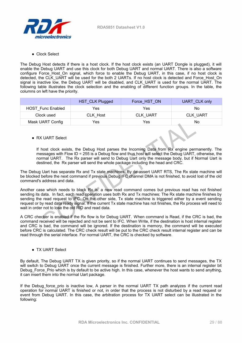
The Debug Host detects if there is a host clock. If the host clock exists (an UART Dongle is plugged), it will enable the Debug UART and use this clock for both Debug UART and normal UART. There is also a software configure Force_Host_On signal, which force to enable the Debug UART, in this case, if no host clock is detected, the CLK_UART will be used for the both 2 UARTs. If no host clock is detected and Force_Host_On signal is inactive low, the Debug UART will be disabled, and CLK_UART is used for the normal UART. The following table illustrates the clock selection and the enabling of different function groups. In the table, the columns on left have the priority.
HST_CLK Plugged Force_HST_ON UART_CLK only
HOST_Func Enabled Yes Yes NoClock used CLK_Host CLK_UART CLK_UART
Mask UART Config Yes Yes No
● RX UART Select
If host clock exists, the Debug Host parses the Incoming Data from Rx engine permanently. The messages with Flow ID = 255 is a Debug flow and thus host will select the Debug UART, otherwise, the normal UART. The Rx parser will send to Debug Uart only the message body, but if Normal Uart is destined, the Rx parser will send the whole package including the head and CRC.
The Debug Uart has separate Rx and Tx state machines. By de-assert UART RTS, The Rx state machine will be blocked before the next command if previous Debug IFC channel DMA is not finished, to avoid lost of the old command's address and data.
Another case which needs to block Rx is: a new read command comes but previous read has not finished sending its data. In fact, each read operation uses both Rx and Tx machines: The Rx state machine finishes by sending the read request to IFC. On the other side, Tx state machine is triggered either by a event sending request or by read data ready signal. If the current Tx state machine has not finishes, the Rx process will need to wait in order not to lose the old RID and read data.
A CRC checker is enabled if the Rx flow is for Debug UART. When command is Read, if the CRC is bad, the command received will be rejected and not be sent to IFC. When Write, if the destination is host internal register and CRC is bad, the command will be ignored. If the destination is memory, the command will be executed before CRC is calculated. The CRC check result will be put to the CRC check result internal register and can be read through the serial interface. For normal UART, the CRC is checked by software.
● TX UART Select
By default, The Debug UART TX is given priority, so if the normal UART continues to send messages, the TX will switch to Debug UART once the current message is finished. Further more, there is an internal register bit Debug_Force_Prio which is by default to be active high. In this case, whenever the host wants to send anything, it can insert them into the normal Uart package.
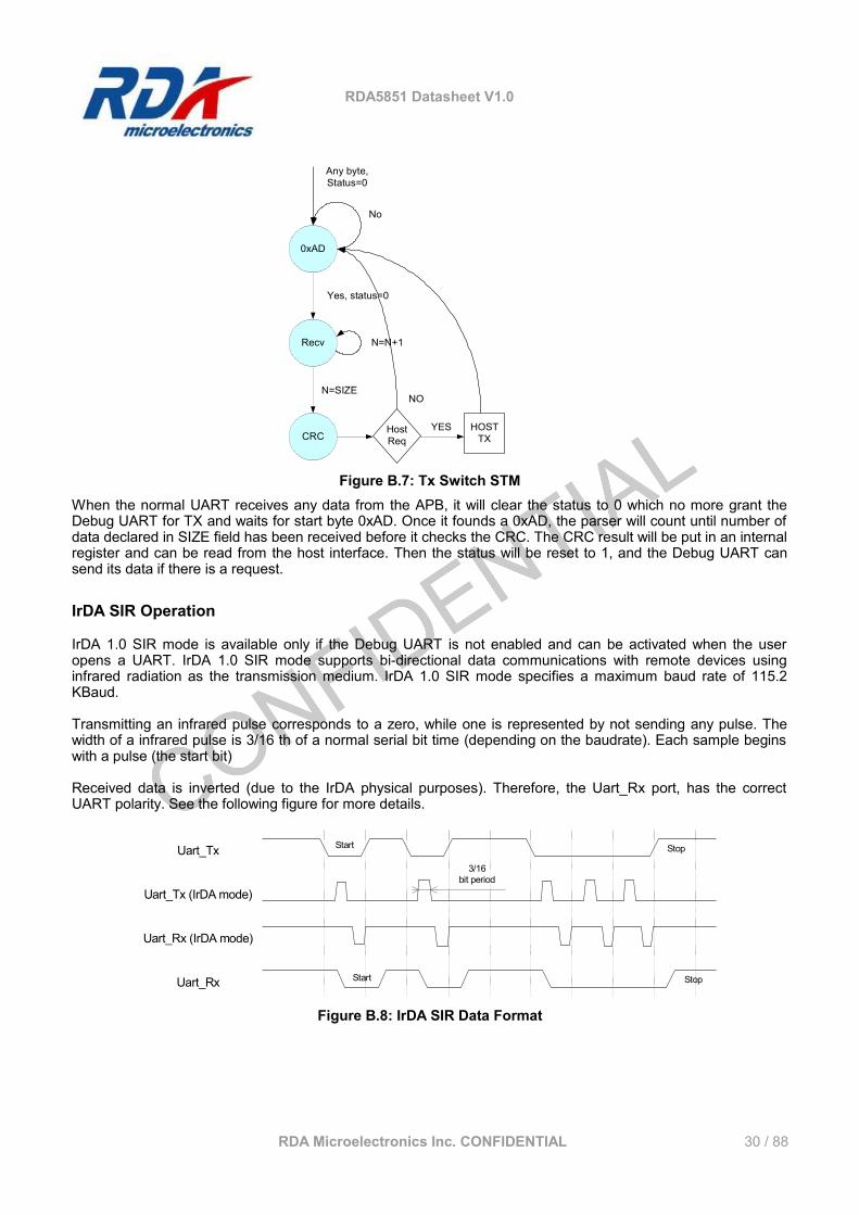
If the Debug_force_prio is inactive low, A parser in the normal UART TX path analyzes if the current read operation for normal UART is finished or not, in order that the process is not disturbed by a read request or event from Debug UART. In this case, the arbitration process for TX UART select can be illustrated in the following:
RDA Microelectronics Inc. CONFIDENTIAL 29 / 88
RDA5851 Datasheet V1.0
Figure B.7: Tx Switch STMWhen the normal UART receives any data from the APB, it will clear the status to 0 which no more grant the Debug UART for TX and waits for start byte 0xAD. Once it founds a 0xAD, the parser will count until number of data declared in SIZE field has been received before it checks the CRC. The CRC result will be put in an internal register and can be read from the host interface. Then the status will be reset to 1, and the Debug UART can send its data if there is a request.
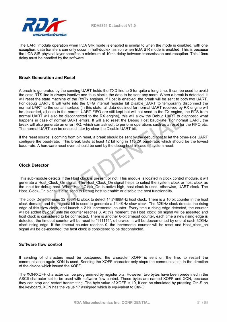
IrDA SIR Operation
IrDA 1.0 SIR mode is available only if the Debug UART is not enabled and can be activated when the user opens a UART. IrDA 1.0 SIR mode supports bi-directional data communications with remote devices using infrared radiation as the transmission medium. IrDA 1.0 SIR mode specifies a maximum baud rate of 115.2 KBaud.
Transmitting an infrared pulse corresponds to a zero, while one is represented by not sending any pulse. The width of a infrared pulse is 3/16 th of a normal serial bit time (depending on the baudrate). Each sample begins with a pulse (the start bit)
Received data is inverted (due to the IrDA physical purposes). Therefore, the Uart_Rx port, has the correct UART polarity. See the following figure for more details.
RDA Microelectronics Inc. CONFIDENTIAL 30 / 88
Figure B.8: IrDA SIR Data Format
Uart_Tx
Uart_Tx (IrDA mode)
Uart_Rx (IrDA mode)
Uart_Rx
Start
Start Stop
Stop
3/16bit period
0xAD
Yes, status=0
Recv
N=SIZE
N=N+1
CRC
No
Any byte,Status=0
HOSTTX
HostReq
YES
NO
RDA5851 Datasheet V1.0
The UART module operation when IrDA SIR mode is enabled is similar to when the mode is disabled, with one exception: data transfers can only occur in half-duplex fashion when IrDA SIR mode is enabled. This is because the IrDA SIR physical layer specifies a minimum of 10ms delay between transmission and reception. This 10ms delay must be handled by the software.
Break Generation and Reset
A break is generated by the sending UART holds the TXD line to 0 for quite a long time. It can be used to avoid the case RTS line is always inactive and thus blocks the data to be sent any more. When a break is detected, it will reset the state machine of the Rx/Tx engines. If Host is enabled, the break will be sent to both two UART. For debug UART, It will write into the CFG internal register bit Disable_UART to temporarily disconnect the normal UART to the serial interface (in this state, all data destined for normal UART received by RX engine will be discarded, all data in the normal UART FIFO are still kept but will not send to the TX engine, the RTS from normal UART will also be disconnected to the RX engine), this will allow the Debug UART to diagnostic what happens in case of normal UART errors. It will also reset the Debug Host baud-rate. For normal UART, the break will also generate an error IRQ, which can ask soft to perform operations such as a reset for the FIFO etc. The normal UART can be enabled later by clear the Disable UART bit.
If the reset source is coming from pin reset, a break should be sent by the debug host to let the other-side UART configure the baud-rate. This break lasts at least 12 bit long in 115.2K baud-rate, which should be the lowest baud-rate. A hardware reset event should be sent by the debug host in case of system reset.
Clock Detector
This sub-module detects if the Host clock is present or not. This module is located in clock control module, it will generate a Host_Clock_On signal. The Host_Clock_On signal helps to select the system clock or host clock as the input for debug host. When Host_Clock_On is active high, host clock is used, otherwise, UART clock. The Host_Clock_On signal is also send to Debug host to enable or disable the host functionality.
The clock Detector uses 32.768KHz clock to detect 14.7468MHz host clock. There is a 10 bit counter in the host clock domain, and the highest bit is used to generate a 14.4KHz slow clock. The 32KHz clock detects the rising edge of this slow clock, and launch a 2-bit incremental counter. Every time a rising edge detected, the counter will be added by one, until the counter reaches 3. At this moment, the Host_clock_on signal will be asserted and host clock is considered to be connected. There is another 6-bit timeout counter, each time a new rising edge is detected, the timeout counter will be reset to “111111”, otherwise, it will be decremented by one at each 32KHz clock rising edge. If the timeout counter reaches 0, the incremental counter will be reset and Host_clock_on signal will be de-asserted, the host clock is considered to be disconnected.
Software flow control
If sending of characters must be postponed, the character XOFF is sent on the line, to restart the communication again XON is used. Sending the XOFF character only stops the communication in the direction of the device which issued the XOFF.
The XON/XOFF character can be programmed by register bits. However, two bytes have been predefined in the ASCII character set to be used with software flow control. These bytes are named XOFF and XON, because they can stop and restart transmitting. The byte value of XOFF is 19, it can be simulated by pressing Ctrl-S on the keyboard. XON has the value 17 assigned which is equivalent to Ctrl-Q.
RDA Microelectronics Inc. CONFIDENTIAL 31 / 88
RDA5851 Datasheet V1.0
Backslash '/' can be added before XON, XOFF and '/' to signifies their original values instead of flow control marks.
B.II.3 Serial Peripheral Interface (SPI)This module is a master interface for a synchronous serial link, it can be configured to be compatible with Motorola SPI or to comply with some various synchronous serial protocols.
RDA5851 includes 2 general purpose SPIs and 1 SPI dedicated to PMU, Analog block integrated modules.
Features
● SPI1 has 3 chip selects● SPI2 has 2 chip selects● 2 selectable data input.● programmable clock polarity.● programmable data frame size (from 4 to 32 bits).● 16 x 8 bits transmit FIFO.● 16 x 8 bits receive FIFO.● a few delay options (time between CS, clocks and data).● received pattern matching before filling RX FIFO (SD-MMC read block feature)● transmit zero when TX FIFO empty (for generating dummy data during pattern matching read)● can be controlled by LPS (an new frame is not started until LPS allows it)● direct pin control to force value to 0, 1 or input.● special read mode with output enable control of the DO pin (selected input should be multiplexed with
DO pin to use this feature)
B.II.4 I2CI2C is a two-wire, bi-directional serial bus that provides a simple and efficient method of data exchange between devices. It is most suitable for applications requiring occasional communication over a short distance between many devices. The I2C standard is a true multi-master bus including collision detection and arbitration that prevents data corruption if two or more masters attempt to control the bus simultaneously.
The interface defines 3 transmission speeds:• Normal: 100Kbps• Fast: 400Kbps• High speed: 3.5Mbps
Only 100Kbps and 400Kbps modes are supported directly.
RDA5851 Chip includes 3xI2C masters.
Features
• Compatible with Philips I2C standard
RDA Microelectronics Inc. CONFIDENTIAL 32 / 88
RDA5851 Datasheet V1.0
• Multi Master Operation• Software programmable clock frequency• Clock Stretching and Wait state generation• Software programmable acknowledge bit• Interrupt or bit-polling driven byte-by-byte data-transfers• Arbitration lost interrupt, with automatic transfer cancellation• Start/Stop/Repeated Start/Acknowledge generation• Start/Stop/Repeated Start detection• Bus busy detection• Supports 7 and 10bit addressing mode• Operates from a wide range of input clock frequencies
Operations
• I2C System configuration
The I2C system uses a serial data line (SDA) and a serial clock line (SCL) for data transfers. All devices connected to these two signals must have open drain or open collector outputs. The logic AND function is exercised on both lines with external pull-up resistors.
Data is transferred between a Master and a Slave synchronously to SCL on the SDA line on a byte-by-byte basis. Each data byte is 8 bits long. There is one SCL clock pulse for each data bit with the MSB being transmitted first. An acknowledge bit follows each transferred byte. Each bit is sampled during the high period of SCL; therefore, the SDA line may be changed only during the low period of SCL and must be held stable duringthe high period of SCL. A transition on the SDA line while SCL is high is interpreted as a command (see START and STOP signals).
• I2C protocol
START signalWhen the bus is free/idle, meaning no master device is engaging the bus (both SCL and SDA lines are high), a master can initiate a transfer by sending a START signal. A START signal, usually referred to as the S-bit, is defined as a high-to-low transition of SDA while SCL is high. The START signal denotes the beginning of a new data transfer. A Repeated START is a START signal without first generating a STOP signal. The master uses this method to communicate with another slave or the same slave in a different transfer direction (e.g. from writing to a device to reading from a device) without releasing the bus.
The I2C master generates a START signal when the STA-bit in the Command Register is set and the RD or WR bits are set. Depending on the current status of the SCL line, a START or Repeated START is generated.
Slave address transferThe first byte of data transferred by the master immediately after the START signal is the slave address. This is a seven-bits calling address followed by a RW bit. The RW bit signals the slave the data transfer direction. No two slaves in the system can have the same address. Only the slave with an address that matches the one transmitted by the master will respond by returning an acknowledge bit by pulling the SDA low at the 9 th SCL clock cycle.
Note: The I2C master supports 10bit slave addresses by generating two address transfers. See the Philips I2C specifications for more details.
The I2C master treats a Slave Address Transfer as any other write action. Store the slave device’s address in the Transmit Register and set the WR bit. The I2C master will then transfer the slave address on the bus.
Data Transfer
RDA Microelectronics Inc. CONFIDENTIAL 33 / 88
RDA5851 Datasheet V1.0
Once successful slave addressing has been achieved, the data transfer can proceed on a byte-by-byte basis in the direction specified by the RW bit sent by the master. Each transferred byte is followed by an acknowledge bit on the 9th SCL clock cycle. If the slave signals a No Acknowledge, the master can generate a STOP signal to abort the data transfer or generate a Repeated START signal and start a new transfer cycle.
If the master, as the receiving device, does not acknowledge the slave, the slave releases the SDA line for the master to generate a STOP or Repeated START signal.
To write data to a slave, store the data to be transmitted in the Transmit Register and set the WR bit. To read data from a slave, set the RD bit. During a transfer the core set the TIP flag, indicating that a Transfer is In Progress. When the transfer is done the TIP flag is reset, the IF flag set and, when enabled, an interrupt generated. The Receive Register contains valid data after the IF flag has been set. The user may issue a new write or read command when the TIP flag is reset.
Stop signalThe master can terminate the communication by generating a STOP signal. A STOP signal, usually referred to as the P-bit, is defined as a low-to-high transition of SDA while SCL is at logical ‘1’.
• Arbitration Procedure
Clock SynchronizationThe I2C bus is a true multi-master bus that allows more than one master to be connected on it. If two or more masters simultaneously try to control the bus, a clock synchronization procedure determines the bus clock. Because of the wired-AND connection of the I2C signals a high to low transition affects all devices connected to the bus. Therefore a high to low transition on the SCL line causes all concerned devices to count off their low period. Once a device clock has gone low it will hold the SCL line in that state until the clock high state is reached. Due to the wired-AND connection the SCL line will therefore be held low by the device with the longest low period, and held high by the device with the shortest high period.
Clock stretching
Slave devices can use the clock synchronization mechanism to slow down the transfer bit rate. After the master has driven SCL low, the slave can drive SCL low for the required period and then release it. If the slave’s SCL low period is greater than the master’s SCL low period, the resulting SCL bus signal low period is stretched, thus inserting wait-states.
B.II.5 General Purpose Input Output
RDA5851 GPIO modules has configurable number of General Purpose Input or Output ports (GPIO) and General Purpose Output port(GPO). There are up to 32 GPIOs and 12 GPOs. GPIO are used to control external chips, or to get external events. They can be used as inputs or outputs. As input, 8 of them can be configured to trigger an interruption (GPIO0 to GPIO7). The IRQ could be generated on edge or level.
Features
● *Up to 32 GPIOs configurable as input or output.● *Up to 12 GPOs.● 8 of the GPIOs can generate interrupt. Various Interrupt triggered mode.
○ Rising/Falling edge.
RDA Microelectronics Inc. CONFIDENTIAL 34 / 88
RDA5851 Datasheet V1.0
○ High/Low level.*Maybe not all of the GPIOs/GPOs can be used because a few are not packaged to the pin pad due to the limitation of the total pin numbers. Please refer to the details of reference design.
B.II.6 KeypadThe RDA5851 keypad is a matrix of 8 rows and 8 columns. Keypad module provides key press, key release detecting mechanism. Each time a key is pressed, keypad module will sense it and will begin to scan the keypad by alternatively driving each column until all keys are released. Besides the keypad matrix, the module also detects key ON, which is an independent input.
The Keypad will send IRQ when either key press or key release event occurs. It can also send IRQ repeatedly when one or several keys are pressed long time. Debounce mechanism is provided to avoid glitches, the time of debounce is programmable.
Any combination of two keys pressed can be detected simultaneously, if certain rules are expected, up to 10 keys can be detected at the same time. However, the following case should be avoided: Note the key at column i1 and row i2 as key(i1, i2). If key(a,b) and key(c,d) is pressed at the same time, then press either key(a,d) or key(b,c) will cause a detection error. The key scanner will consider all of the four keys have been pressed.
Features
● Generate IRQ for both key press and release events. ● Generate IRQ if one or several keys are pressed long time. The IRQ is repeated with a configurable
interval from 1*debounce time to 64*debounce time. ● provide debounce mechanism. Configurable debounce time maximum 480 ms.● Detect two simultaneous key press with any combination. Detect up to 10 keys at the same time if
certain patterns are excluded. (i.e. Keypad module can detect entire one row and one column without crossed key).
● Key ON detection.● Possible to disable some rows and columns of keypad matrix.
B.II.7 Pulse Width Modulation (PWM)The PWM module generates four independent PWM outputs, utilizing three specialized modulation schemes. There are two Pulse Width Light (PWL) outputs designed for driving LEDs with varying brightness, one Pulse Width Tone (PWT) output for generating tones, and one Light Pulse Generator (LPG) output for blinking an LED at visibly recognizable frequencies.
Features
● Pulse Width Tone (PWT)○ Generates square wave output capable of driving piezo electric speaker○ Variable frequency between 349Hz and 5276Hz with 12 half-tone frequencies per octave○ Volume control (coarse)
● Light Pulse Generation (LPG)○ Adjustable blinking period from 125 ms to 3 seconds○ Adjustable on-time from 15 ms to ¼ second.
RDA Microelectronics Inc. CONFIDENTIAL 35 / 88
RDA5851 Datasheet V1.0
● Two separate Pulse Width Light (PWL)○ Pseudo random bit sequence with output on-time proportional to a programmed threshold value○ Minimizes flicker
Typical Operation
The PWT module generates a 'symmetric' square wave whose duty cycle is variable between 0 and 50% (as opposed to the pseudo-random output in the case of PWL). The generated tones have been tested for half-tone frequency increments between 349Hz and 5276Hz. Basic volume control can be achieved by varying the duty cycle, but the actual values depend on the final frequency and the buzzer being used. Also, changing the duty cycle will change the harmonics, and thus will have an effect on the pitch of the note, but for very coarse operation, this mechanism should suffice.
The Light Pulse Generator (LPG) can be used for blinking a LED at adjustable periods for various signaling purposes. The period is variable between 125 ms through 3 seconds. The length of time the LED will stay on is also programmable multiples of 256/16kHz up to ¼ of a second.
The two PWL modules are optimized for driving back lights and LEDs where pseudo-random pulses with a programmable average on-time are desired. The resulting output will be non-symmetric and will help reduce flicker effects. A low-pass filter can be added to convert the PWL output to an analog value.
B.II.8 CalendarThe Calendar module provides date and time information. It works on the 32.768 KHz oscillator with independent power supply. Calendar module is able to generate an IRQ repetitively at certain interval, which can be programmed to 1 second, 1 minute or 1 hour. In addition to provide timing data, alarm interrupt is generated and it is also used to power-up the baseband core by sending wakeup signal. The year span is supported from 2000 to 2127, the maxim day of each month is stored in the calendar block, which depends on the leap year condition.
Features
● Independent power supply. ● Counters for second, minute, hour, day, month, year and day of week.● Maxim day of each month stored in module, leap year supported.● Alarm generate, wakeup triggered by alarm. Alarm IRQ.● Periodical IRQ for certain intervals.
B.II.9 Timers
RDA5851 includes 1 OS timer, 1 watchdog timer and 1 hardware delay timers. The OS timer serves for OS, and has Ticks of 16384 Hz. It is a decrement timer and the initial value can be programmed. When the OS timer reaches 0, it will cause an interruption. After that, the OS timer will either stop or restart with the initial value (loop mode) or wrap to maximum value (wrap mode).
The watchdog timer can be used to protect against system failure or software mistakes by reinitializing the system. When it’s no longer servicing the watchdog timer, the Watchdog Timer operations are almost identical to the OS Timer. In addition when the counter reaches 0 it can trigger a System Reset. To use the Watchdog function, the software should reload the Watchdog Timer on a periodic basis to avoiding the Watchdog Timer to reach 0 and trigger an interrupt or a system reset (depending on configuration).
RDA Microelectronics Inc. CONFIDENTIAL 36 / 88
RDA5851 Datasheet V1.0
The hardware delay timer is an incremental timer. It has Ticks of 16384 Hz. This timer is free running, and the value will be reset to 0. The timer value will wrap to 0 after 0xfffffff, and will generate an IRQ when wrap. The hardware delay timer can also generate an interval IRQ which can be configured to every 1 /8 second,1/4 second, 1/2 second, or 1 second.
The timers module has two IRQs. One dedicated for OS timer, the other is used by all the other timers. (including watchdog timer, hardware delay timer)
Features
● 1 24-bit decremental timer for OS.● 1 32-bit incremental hardware delay timer.● 1 24-bit decremental watchdog timer.● Multiple IRQ sources: timers wrap, interval arrives.
B.II.10 Debug Port (EXL, PXTS, Signal Spy)The DEBUG_PORT module:
- Provide 4 watches.- Storing the last execution address of the selected CPU in the event of a watchdog reset. This value is not reset on any system reset and can be read when the system was recovered from the watchdog reset.- Data packet transfer: debugging tool configurable in 4 different modes:
Features
● Access to the last PC of the selected CPU when a watchdog reset occurs.● Mode Debug_Port_Off : This mode switch off the module● Mode Exl : This mode record all the CPU Jump start address send to the Romulator. Generate a
strobe and output the selected CPU's PC.● Mode Pxts : This mode record all the serial events analyzed by Coolprofile. Generate a Strobe and
output the Pxts tag.Through Pxts Enable decoding, we will be able to select one Pxts_tag into 16 Pxts_tag defined.
● Mode Pxts_Exl: this mode enable both mode PXTS and EXL. PXTS mode has a highest priority compare to mode EXL.
● Mode Signal_Spy : This mode spy the signals for the debug purpose(Describe the IOCore muxing for IO mode configuration)
B.II.11 General Purpose Analog to Digital Converter (GP ADC)The GPADC module controls the analog module of general purpose analog to digital converter, which is capable of measuring one of 2 analog external inputs of the chip. The 2 external inputs can be connected to sensors to measure battery voltage, battery temperature, temperature, accessory ID, remote control, or other low frequency analog signal within the specified voltage range.
RDA Microelectronics Inc. CONFIDENTIAL 37 / 88
RDA5851 Datasheet V1.0
The GPADC is active periodically at a variable rate if at least one channel is enabled. The value of each channel is readable through the APB interface.
Features
● Up to 2 analog external channels.● Automatic measurement at variable rate.● Interrupt when programmed threshold is passed.
Operation
By default, GPADC works in functional mode, GPADC is active periodically at a variable rate and measures all the enabled channel (up to 2) each time.
There is also a test mode for debug purpose, in which GPADC receives a start measure command from APB, and do a measurement once.
Usually, the one GPADC is used for mic detect, and another is for user defined function.
B.II.12 Timing Control Unit and Low Power Synchronizer (TCU+LPS)
The Timing Control Unit handle the scheduling of individual events with a quarter bit precision.
The TCU is based on a quarter bit counter (13/12 MHz = 1.083 MHz), which wraps at a programmable value. An interruption is generated when the counter wraps (Frame interrupt). The current value of this counter is available at any time. The wrap value can be set at any time. To assure a predictable behavior this value should only be set by the programmer “far” from the wrap time, to make sure this new value will be taken into account the next time.
The programmer can define events associated to particular counter values (dates). When the counter equals the given date, the action associated to the event will take place.
The event are contained in a table of events split into a programming table and an active table. Only the events in the active table are compared to the counter value. The programming table table allows to prepare a full sequence of events which will be transfered to the active table when the counter wraps.
A force signal allows to transfer events from the programming table to the active table immediately.
The LPS Low Power Synchronizer is a part of the TCU, it is responsible for maintaining the time base while running at a slower clock (32kHz) for power saving.
TCU Features
● Quarter bit precision.● 60 entries event table.● Programmable counter wrap value.
LPS Features
RDA Microelectronics Inc. CONFIDENTIAL 38 / 88
RDA5851 Datasheet V1.0
● Allow skipping frames by masking the TCU Frame Interrupt.● Calibration of the 32kHz clock against the System Clock with an accuracy of 4 System clocks during a
programmable time to reach wanted rate accuracy.● Low power counters (32kHz) can maintain timebase while System clock is suspended.● A hardware state machine can assist the CPU for the power up after each exit of the low power mode.
B.II.13 System AHB Monitor (Sys AHBC Mon) This monitor connected to the System AHB bus can measure several bandwidth and latency information.
Features
● 8 configurable time windows:● 4 asynchronous for gradually going from accuracy to reactivity of the measures.● 4 based on frame for GMS related measurements● Peak or mean measures.● Selection between several resources:● Global bus usage.● Bus usage and latency of access for a particular master.● Bus usage, number of access and duration of access for a slave.● High time, number of rise and duration of high time for a resource selected via the signal select of the
debug port.
Mean calculation
Measures are always relative to the time window. Mean latency or duration has to be calculated by dividing the total latency / duration measured by the number of accesses.
Special resource monitoring
The Signal_Select0 and Signal_Select1 signals can be monitored to estimate latency of IRQ handling, or measure any latency/usage of software part. This last case can be achieved by setting Signal_Select0 to Watch(n) in the debug port configuration, monitoring the Signal_Select0 signal; by setting and clearing the Watch(n) during code to profile, you can measure the mean time spent.
B.II.14 System IRQ Controller (Sys IRQ)In RDA5851, the interruptions are generated by the modules, they can be filtered at the module level (the mask must be configured in each corresponding module's registers), then they are filtered by the System or Base Band IRQ Controller (the mask is set in System IRQ Control or Base Band IRQ Control registers). The interrupts must be cleared in the corresponding module.
For power saving, one CPU can shut down its own clock. A special wakeup mask allows re-enabling the clock when an interruption enabled in this mask is triggered..
Features
RDA Microelectronics Inc. CONFIDENTIAL 39 / 88
RDA5851 Datasheet V1.0
● A mask at the module level.● A mask at the IRQ Control level.● A second Mask for Pulse IRQ (that are not masked in the module)● Wakeup mask.● Sleep Register● Driving IRQ inputs to the CPU (6 lines)
B.II.15 USB Controller
Features
● Fully compliant to USB Specification Version 1.1● Slave Full Speed (12Mbps) Device● Integrated USB Transceiver ● Supports Control, Interrupt, Bulk and Isochronous transfer● 4 Endpoint with FIFO:
○ One Bi-directional Control Endpoint (EP0)○ Three soft configurable Bi-directional Endpoints
● SRAM FIFO : 264 words (32bits)
B.II.16 Graphic Overlay United Display Accelerator (GOUDA)The GOUDA module handles various graphic operations used to compose and display images on LCD.
These operations : colour space conversion, resizing, landscape/portrait rotation and layer blending and overlay are very CPU-cycle consuming, and also especially bandwidth hungry as for every single operation, one or several images have be loaded, processed and temporary rewritten into memory before being actually sent to the LCD display.
GOUDA module relieve the CPU by both handling the pixel processing itself and also by using the minimum memory bandwidth as it only loads once needed data and outputs the final result directly.
GOUDA can handle 4 video layers and output the resulting image composition directly to the LCD interface. The graphic subsystem have the following capabilities:
– 4 distinct video sources can be blended to produce final output :– Layer 0 (aka video layer) :
– Input formats : YUV4:2:0 planar (IYUV, YV12), YUV4:2:2 pixel-packed (UYVY, YUY2), RGB565
– YUV to RGB565 conversion (CCIR601 component video standard definition)– Image resizing (separate H and V ratios, from 1/4th to 4x each direction, 8bit fractional step)– adjustable layer depth– per-layer alpha blending– chroma-key with simple range handling (bit-masking based)
– Layer 1-3 (aka overlay layers):– Input formats : RGB565, ARGB8888– fixed depth– per-layer alpha blending– chroma-key with simple range handling (bit-masking based)– per-pixel alpha blending (for ARGB)
– Region Of Interest (ROI) handling for partial refresh of the LCD screen.
RDA Microelectronics Inc. CONFIDENTIAL 40 / 88
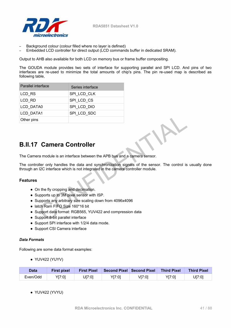
RDA5851 Datasheet V1.0
– Background colour (colour filled where no layer is defined)– Embedded LCD controller for direct output (LCD commands buffer in dedicated SRAM).
Output to AHB also available for both LCD on memory bus or frame buffer compositing.
The GOUDA module provides two sets of interface for supporting parallel and SPI LCD. And pins of two interfaces are re-used to minimize the total amounts of chip's pins. The pin re-used map is described as following table,
Parallel interface Series interface
LCD_RS SPI_LCD_CLKLCD_RD SPI_LCD_CSLCD_DATA0 SPI_LCD_DIOLCD_DATA1 SPI_LCD_SDCOther pins
B.II.17 Camera ControllerThe Camera module is an interface between the APB bus and a camera sensor.
The controller only handles the data and synchronization signals of the sensor. The control is usually done through an I2C interface which is not integrated in the camera controller module.
Features
● On the fly cropping and decimation. ● Supports up to 3M pixel sensor with ISP. ● Supports any arbitrary size scaling down from 4096x4096 ● latch Ram FIFO Size 160*16 bit ● Support data format: RGB565, YUV422 and compression data● Support 8-bit parallel interface● Support SPI interface with 1/2/4 data mode.● Support CSI Camera interface
Data Formats
Following are some data format examples:
● YUV422 (YUYV)
Data First pixel First Pixel Second Pixel Second Pixel Third Pixel Third PixelEven/Odd Y[7:0] U[7:0] Y[7:0] V[7:0] Y[7:0] U[7:0]
● YUV422 (YVYU)
RDA Microelectronics Inc. CONFIDENTIAL 41 / 88
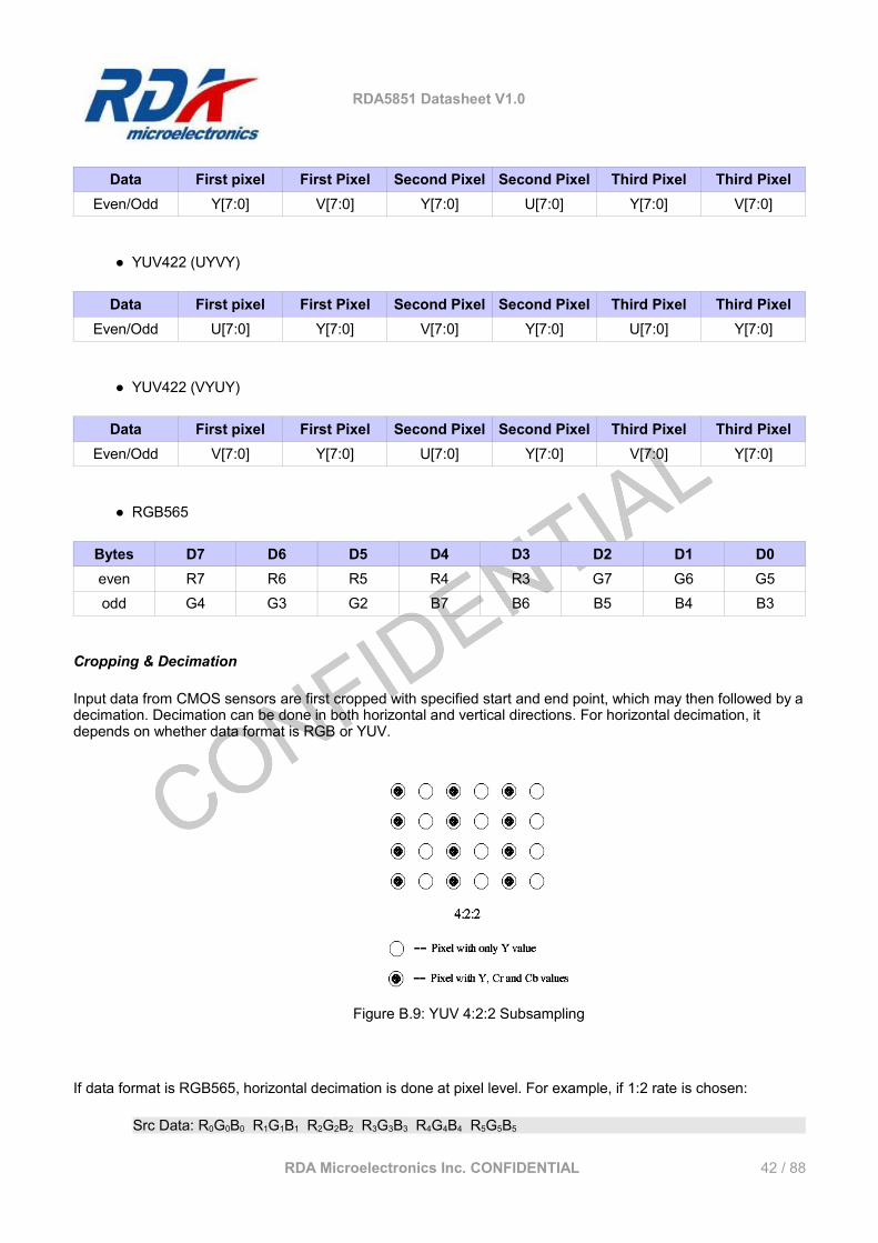
RDA5851 Datasheet V1.0
Data First pixel First Pixel Second Pixel Second Pixel Third Pixel Third PixelEven/Odd Y[7:0] V[7:0] Y[7:0] U[7:0] Y[7:0] V[7:0]
● YUV422 (UYVY)
Data First pixel First Pixel Second Pixel Second Pixel Third Pixel Third PixelEven/Odd U[7:0] Y[7:0] V[7:0] Y[7:0] U[7:0] Y[7:0]
● YUV422 (VYUY)
Data First pixel First Pixel Second Pixel Second Pixel Third Pixel Third PixelEven/Odd V[7:0] Y[7:0] U[7:0] Y[7:0] V[7:0] Y[7:0]
● RGB565
Bytes D7 D6 D5 D4 D3 D2 D1 D0even R7 R6 R5 R4 R3 G7 G6 G5odd G4 G3 G2 B7 B6 B5 B4 B3
Cropping & Decimation
Input data from CMOS sensors are first cropped with specified start and end point, which may then followed by a decimation. Decimation can be done in both horizontal and vertical directions. For horizontal decimation, it depends on whether data format is RGB or YUV.
Figure B.9: YUV 4:2:2 Subsampling
If data format is RGB565, horizontal decimation is done at pixel level. For example, if 1:2 rate is chosen:
Src Data: R0G0B0 R1G1B1 R2G2B2 R3G3B3 R4G4B4 R5G5B5
RDA Microelectronics Inc. CONFIDENTIAL 42 / 88
RDA5851 Datasheet V1.0
Dst Data: R0G0B0 R2G2B2 R4G4B4
If data format is YUV422, horizontal decimation is should regroup some pixels. For example, if 1:2 rate is chosen:
Src Data: Y0U0Y1V0 Y2U1Y3V1 Y4U2Y5V2 Y6U3Y7V3 Y8U4Y9V4 Y10U5Y11V5
Dst Data: Y0U0Y2V0 Y4U2Y6V2 Y8U4Y10V4
Another example, if YUV422 1:3 rate is chosen:
Src Data: Y0U0Y1V0 Y2U1Y3V1 Y4U2Y5V2 Y6U3Y7V3 Y8U4Y9V4 Y10U5Y11V5
Dst Data: Y0U0Y3V0 Y6U3Y9V3
For Vertical decimation, data format RGB565/555/444 or YUV422 will be the same, vertical decimation is done at line level. For example, if 1:2 rate is chosen:
Src Data: Line0 Line1 Line2 Line3 Line4 Line5
Dst Data: Line0 Line2 Line4
FIFO
Rx Data FIFO is in APB domain. So FIFO_Write signal from CAM_PIXCLK domain will be synchronized to APB domain. This requires APB clock frequency faster than CAM_PIXCLK frequency * 0.75. For example, if RGB565 QXGA 15 frame/s is required, APB CLK freq should > 3.1M pixel * 2 byte per pixel * 15 frame per sec * 0.75 = 70 MHz.
Interface
The Camera module provides two types of interface for camera sensor. One is the traditional 8-bit parallel interface, the other is SPI interface which uses less signal. The two interfaces are share the same pin so that it does not increase the total amounts of chip pins.
The typical connect of 1 data series interface is as following, here the GC6113 and PA6167/6175 are chose for examples.
Parallel Interface SPI interface GC6113 (1 data mode) PAS6167/6175 CSI InterfaceCAM_D0 /CAM_D1 SPI_CAM_CTS CTSCAM_D2 CSI_DN2CAM_D3 CSI_DP2CAM_D4 SPI_CAM_OF OVERFLOW_M CSI_DN1CAM_D5 SPI_CAM_RD OVERFLOW_S CSI_DP1CAM_D6 SPI_CAM_SSN SSN CSI_CKPCAM_D7 SPI_CAM_SCK SCK SCLK CSI_CKN
RDA Microelectronics Inc. CONFIDENTIAL 43 / 88
RDA5851 Datasheet V1.0
CAM_PCLK SPI_CAM_DI SDO0 SDOCAM_VSYNCCAM_CLK CAM_CLK MCLK SYS_CLKCAM_RST I2C_SCL SBCL I2C_SCLCAM_PDN I2C_SDA SBDA I2C_SDA
B.II.18 SD/MMC ControllerThis module connects inner bus and outer SD or MMC card. It receives the inner command and data, transfers it to outer SD or MMC card, and transfer response or data back.
Features
● SD Card Specification Version 2.0 ● SDIO Version 1.10● MMC specification Version 3.1● Hot insertion and removal of media cards will be considered by GPIO module
B.II.19 Audio Interface Analog + I2S (AIF)The Audio Interface (AIF) module is the audio interface between the RDA5851 system and multimedia chip.
AIF can work in master mode in which it generates synchronization signals needed by the multimedia chip, which contains the audio ADC and DAC to convert the serial digital output data to analog audio signal and the input analog signal to serial digital audio data. It can also works in slave mode which uses synchronization signals sent from multimedia chip. Please see below for more details about serial data format.
AIF includes both serious and parallel interface. It is able to support multiple sample rate including 8 kHz, 11.025 kHz, 12kHz, 16 kHz, 22,05 kHz, 24kHz, 32kHz, 44,1 kHz, 48kHz and various data format. AIF can also generate common DTMF, comfort tones and side tone with a configurable gain.
Features
● Common features.○ 4*32-bit RX and 4*32-bit TX FIFO.○ All common DTMF and Comfort Tones can be generated and gained from -15 dB to 0 dB.○ Side Tone fully configurable: Mute or amplification from -36 dB to +6 dB.○ Loop back capabilities for test purposes.
● Serial Interfaces.○ 16-bit mono or stereo samples.○ MSB/LSB configurable.
RDA Microelectronics Inc. CONFIDENTIAL 44 / 88
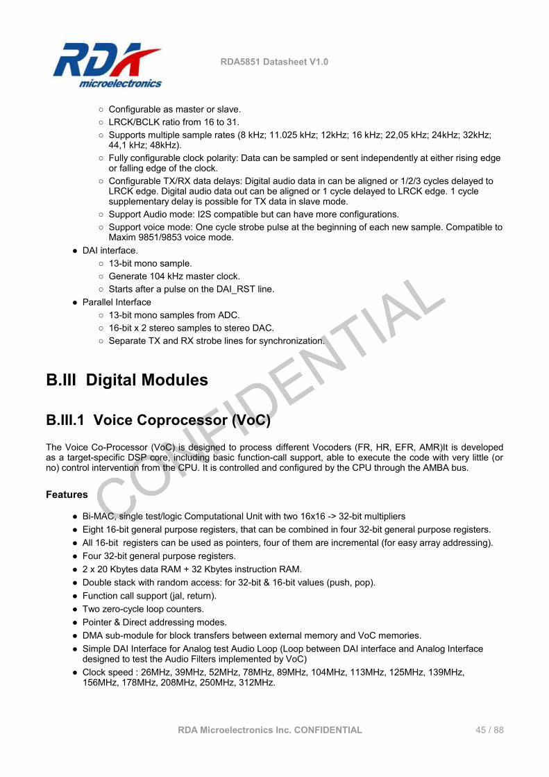
RDA5851 Datasheet V1.0
○ Configurable as master or slave.○ LRCK/BCLK ratio from 16 to 31.○ Supports multiple sample rates (8 kHz; 11.025 kHz; 12kHz; 16 kHz; 22,05 kHz; 24kHz; 32kHz;
44,1 kHz; 48kHz).○ Fully configurable clock polarity: Data can be sampled or sent independently at either rising edge
or falling edge of the clock. ○ Configurable TX/RX data delays: Digital audio data in can be aligned or 1/2/3 cycles delayed to
LRCK edge. Digital audio data out can be aligned or 1 cycle delayed to LRCK edge. 1 cycle supplementary delay is possible for TX data in slave mode.
○ Support Audio mode: I2S compatible but can have more configurations.○ Support voice mode: One cycle strobe pulse at the beginning of each new sample. Compatible to
Maxim 9851/9853 voice mode.● DAI interface.
○ 13-bit mono sample.○ Generate 104 kHz master clock.○ Starts after a pulse on the DAI_RST line.
● Parallel Interface○ 13-bit mono samples from ADC.○ 16-bit x 2 stereo samples to stereo DAC.○ Separate TX and RX strobe lines for synchronization.
B.III Digital Modules
B.III.1 Voice Coprocessor (VoC)The Voice Co-Processor (VoC) is designed to process different Vocoders (FR, HR, EFR, AMR)It is developed as a target-specific DSP core, including basic function-call support, able to execute the code with very little (or no) control intervention from the CPU. It is controlled and configured by the CPU through the AMBA bus.
Features
● Bi-MAC, single test/logic Computational Unit with two 16x16 -> 32-bit multipliers● Eight 16-bit general purpose registers, that can be combined in four 32-bit general purpose registers.● All 16-bit registers can be used as pointers, four of them are incremental (for easy array addressing).● Four 32-bit general purpose registers.● 2 x 20 Kbytes data RAM + 32 Kbytes instruction RAM.● Double stack with random access: for 32-bit & 16-bit values (push, pop).● Function call support (jal, return).● Two zero-cycle loop counters.● Pointer & Direct addressing modes.● DMA sub-module for block transfers between external memory and VoC memories.● Simple DAI Interface for Analog test Audio Loop (Loop between DAI interface and Analog Interface
designed to test the Audio Filters implemented by VoC)● Clock speed : 26MHz, 39MHz, 52MHz, 78MHz, 89MHz, 104MHz, 113MHz, 125MHz, 139MHz,
156MHz, 178MHz, 208MHz, 250MHz, 312MHz.
RDA Microelectronics Inc. CONFIDENTIAL 45 / 88
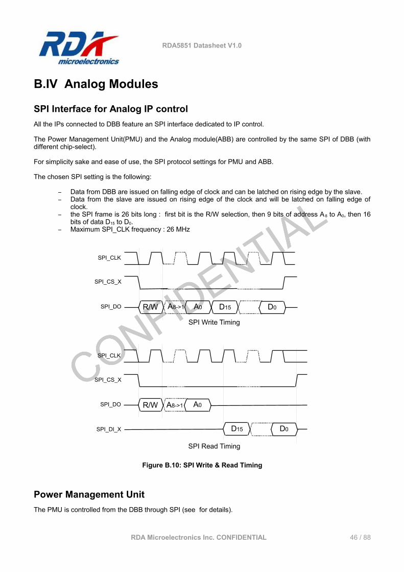
RDA5851 Datasheet V1.0
B.IV Analog Modules
SPI Interface for Analog IP controlAll the IPs connected to DBB feature an SPI interface dedicated to IP control.
The Power Management Unit(PMU) and the Analog module(ABB) are controlled by the same SPI of DBB (with different chip-select).
For simplicity sake and ease of use, the SPI protocol settings for PMU and ABB.
The chosen SPI setting is the following:
– Data from DBB are issued on falling edge of clock and can be latched on rising edge by the slave.– Data from the slave are issued on rising edge of the clock and will be latched on falling edge of
clock.– the SPI frame is 26 bits long : first bit is the R/W selection, then 9 bits of address A 8 to A0, then 16
bits of data D15 to D0.– Maximum SPI_CLK frequency : 26 MHz
Power Management UnitThe PMU is controlled from the DBB through SPI (see for details).
RDA Microelectronics Inc. CONFIDENTIAL 46 / 88
Figure B.10: SPI Write & Read Timing
A0 D15 D0
SPI_CLK
SPI_CS_X
SPI_DO
R/W A0
D15 D0
SPI_CLK
SPI_DO
SPI_DI_X
SPI Write Timing
SPI Read Timing
A8->1
A8->1R/W
SPI_CS_X
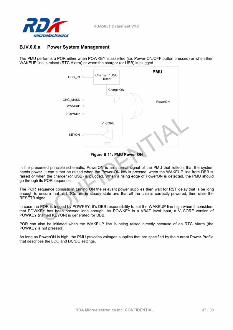
RDA5851 Datasheet V1.0
B.IV.0.0.a Power System Management
The PMU performs a POR either when POWKEY is asserted (i.e. Power-ON/OFF button pressed) or when then WAKEUP line is raised (RTC Alarm) or when the charger (or USB) is plugged.
In the presented principle schematic, PowerON is an internal signal of the PMU that reflects that the system needs power. It can either be raised when the Power-ON key is pressed, when the WAKEUP line from DBB is raised or when the charger (or USB) is plugged. When a rising edge of PowerON is detected, the PMU should go through its POR sequence.
The POR sequence consists in turning ON the relevant power supplies then wait for RST delay that is be long enough to ensure that all LDOs are in steady state and that all the chip is correctly powered, then raise the RESETB signal.
In case the POR is trigged by POWKEY, It's DBB responsibility to set the WAKEUP line high when it considers that POWKEY has been pressed long enough. As POWKEY is a VBAT level input, a V_CORE version of POWKEY (named KEYON) is generated for DBB.
POR can also be initiated when the WAKEUP line is being raised directly because of an RTC Alarm (the POWKEY is not pressed).
As long as PowerON is high, the PMU provides voltages supplies that are specified by the current Power-Profile that describes the LDO and DC/DC settings.
RDA Microelectronics Inc. CONFIDENTIAL 47 / 88
Figure B.11: PMU Power ON
POWKEY
WAKEUPPowerONCHG_MASK
PMU
KEYON
Charger / USBDetect
V_CORE
CHG_IN
ChargerON
RDA5851 Datasheet V1.0
B.IV.0.0.b
The PMU implements multiple power profiles defining the LDOs and DC/DC activation in various modes.
• Default_powerOFF_profile: used when the system is OFF( system has been shut-off or first time battery is plugged...). In this case only V_RTC is provided.
• Default_powerON_profile: used when PowerON is asserted and the POR is trigged, all LDOs that have “reset state ON” are activated.
• Active_power_profile: used once system has booted and decided to switch from Default_powerON_profile. This profile is programmable.
• LP_power_profile: used when the system goes to low-power mode (switch from Active to Low-power through LP_MODE line). This profile is programmable.
RDA Microelectronics Inc. CONFIDENTIAL 48 / 88
Figure B.12: POR triggered by POWKEY press
POWKEY
LDO's supplies
RESETB
WAKEUP
RSTdelay
DBB boots and sets WAKEUP
PowerON
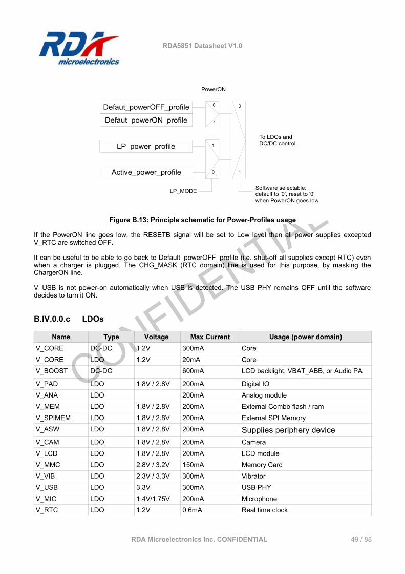
RDA5851 Datasheet V1.0
If the PowerON line goes low, the RESETB signal will be set to Low level then all power supplies excepted V_RTC are switched OFF.
It can be useful to be able to go back to Default_powerOFF_profile (i.e. shut-off all supplies except RTC) even when a charger is plugged. The CHG_MASK (RTC domain) line is used for this purpose, by masking the ChargerON line.
V_USB is not power-on automatically when USB is detected. The USB PHY remains OFF until the software decides to turn it ON.
B.IV.0.0.c LDOs
Name Type Voltage Max Current Usage (power domain)V_CORE DC-DC 1.2V 300mA Core V_CORE LDO 1.2V 20mA CoreV_BOOST DC-DC 600mA LCD backlight, VBAT_ABB, or Audio PA
V_PAD LDO 1.8V / 2.8V 200mA Digital IOV_ANA LDO 200mA Analog module V_MEM LDO 1.8V / 2.8V 200mA External Combo flash / ramV_SPIMEM LDO 1.8V / 2.8V 200mA External SPI MemoryV_ASW LDO 1.8V / 2.8V 200mA Supplies periphery deviceV_CAM LDO 1.8V / 2.8V 200mA Camera V_LCD LDO 1.8V / 2.8V 200mA LCD moduleV_MMC LDO 2.8V / 3.2V 150mA Memory CardV_VIB LDO 2.3V / 3.3V 300mA VibratorV_USB LDO 3.3V 300mA USB PHYV_MIC LDO 1.4V/1.75V 200mA MicrophoneV_RTC LDO 1.2V 0.6mA Real time clock
RDA Microelectronics Inc. CONFIDENTIAL 49 / 88
Figure B.13: Principle schematic for Power-Profiles usage
Defaut_powerON_profile
LP_power_profile
Active_power_profile
LP_MODE Software selectable: default to '0', reset to '0' when PowerON goes low.
To LDOs and DC/DC control
Defaut_powerOFF_profile
PowerON
0
1
0
1
0
1
RDA5851 Datasheet V1.0
B.IV.0.0.d LED Drivers
The PMU implements both LCD backlight and Keypad LED drivers.
There are 4 current sink sources provided for the LCD backlight use, which named as LED1-4.. Each of them can sink 30mA.
The Keypad LED drivers include 3 sink sources as KP_LEDR, KP_LEDG, and KP_LEDB. Each of them can provide 30mA sink current. KP_LED_OUT is voltage feedback current regulator which is suggested to connect to the anode of the keypad LEDs.
Both LCD backlight and Keypad LED drivers can be adjusted driver capability by software via changing current or PWM settings.
B.IV.0.0.e Charger Circuit
The RDA5851 integrates the most of charger circuits, except for a few components such as one PMOS, one accurate resistor and one diode, which should be applied externally.
When the charger is on, this block controls the charging phase and turns on the appropriate LDOs according to the battery status. If the voltage is greater than 4.2~ 4.4 V, charging is stopped immediately to prevent permanent damage to the battery.
Battery charging states include No Charge mode, Constant Current (CC) charge mode (pre-charge, constant current), and Constant Voltage (CV) charge mode. No matter what state the phone is in, the PMIC charger handles the charging state transition. A typical charging process is described as what the Figure 5 shows.
RDA Microelectronics Inc. CONFIDENTIAL 50 / 88
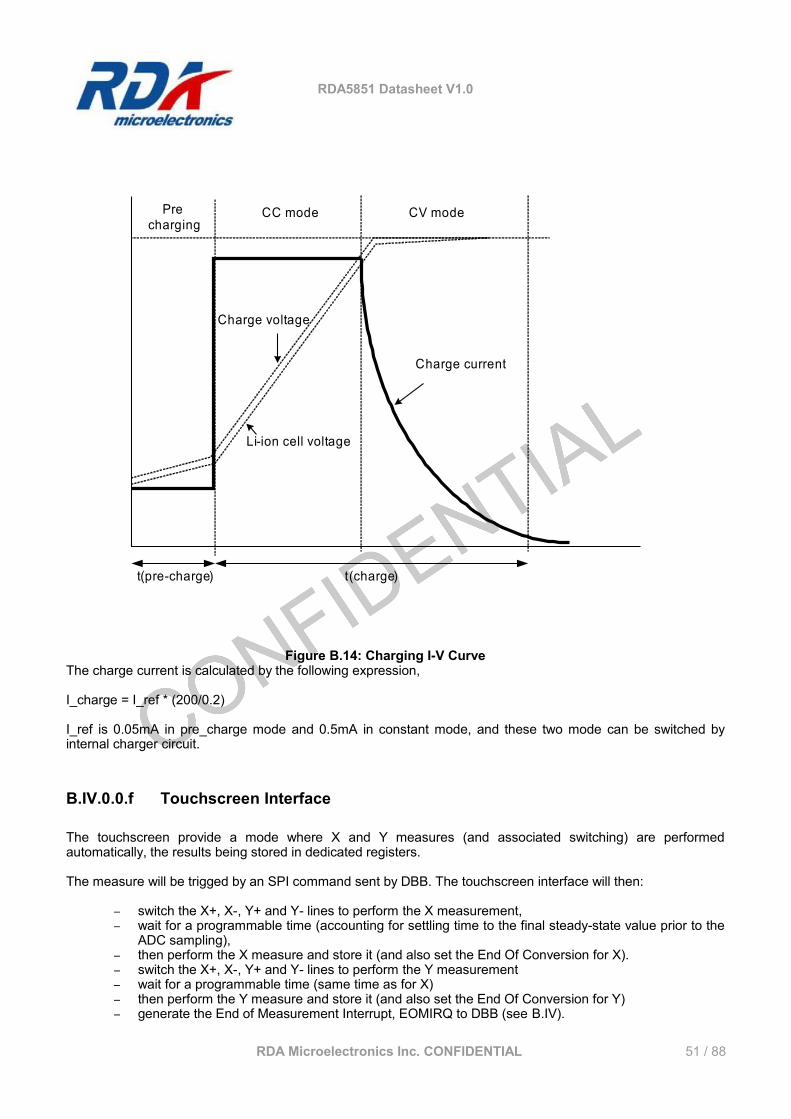
RDA5851 Datasheet V1.0
Figure B.14: Charging I-V CurveThe charge current is calculated by the following expression,
I_charge = I_ref * (200/0.2)
I_ref is 0.05mA in pre_charge mode and 0.5mA in constant mode, and these two mode can be switched by internal charger circuit.
B.IV.0.0.f Touchscreen Interface
The touchscreen provide a mode where X and Y measures (and associated switching) are performed automatically, the results being stored in dedicated registers.
The measure will be trigged by an SPI command sent by DBB. The touchscreen interface will then:
– switch the X+, X-, Y+ and Y- lines to perform the X measurement,– wait for a programmable time (accounting for settling time to the final steady-state value prior to the
ADC sampling),– then perform the X measure and store it (and also set the End Of Conversion for X).– switch the X+, X-, Y+ and Y- lines to perform the Y measurement– wait for a programmable time (same time as for X)– then perform the Y measure and store it (and also set the End Of Conversion for Y)– generate the End of Measurement Interrupt, EOMIRQ to DBB (see B.IV).
RDA Microelectronics Inc. CONFIDENTIAL 51 / 88
Precharging
t(pre-charge) t(charge)
CC mode CV mode
Charge current
Charge voltage
Li-ion cell voltage
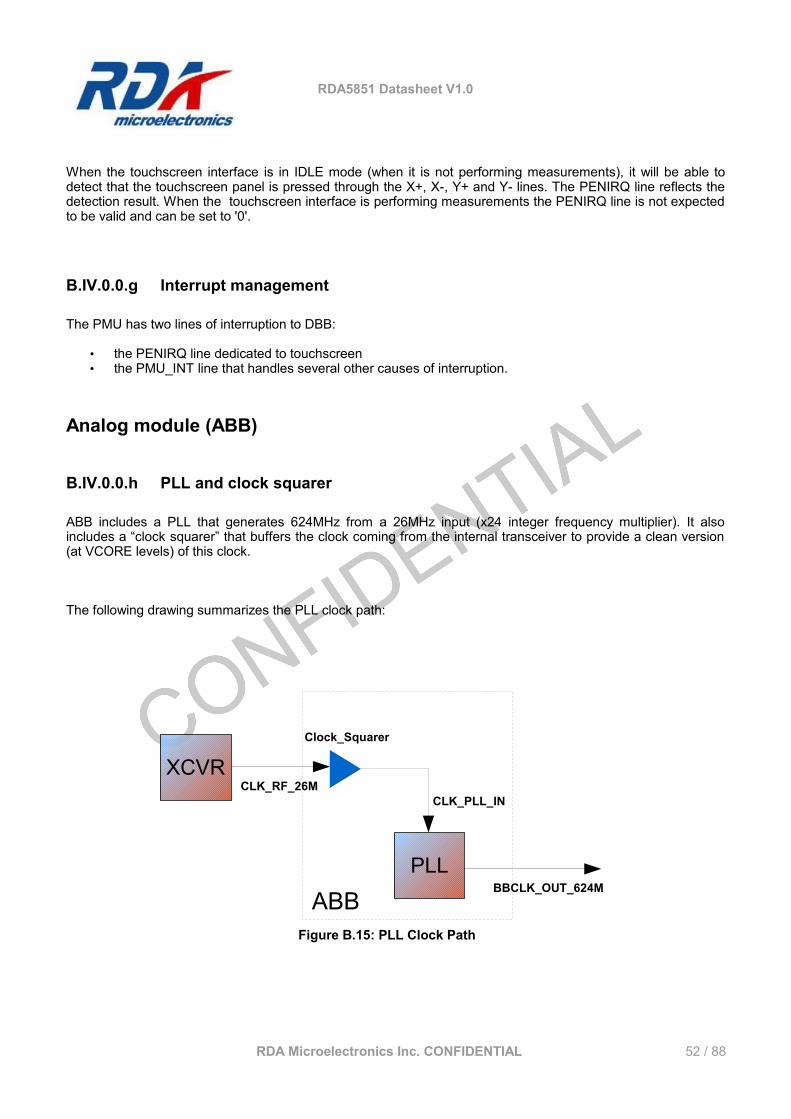
RDA5851 Datasheet V1.0
When the touchscreen interface is in IDLE mode (when it is not performing measurements), it will be able to detect that the touchscreen panel is pressed through the X+, X-, Y+ and Y- lines. The PENIRQ line reflects the detection result. When the touchscreen interface is performing measurements the PENIRQ line is not expected to be valid and can be set to '0'.
B.IV.0.0.g Interrupt management
The PMU has two lines of interruption to DBB:
• the PENIRQ line dedicated to touchscreen• the PMU_INT line that handles several other causes of interruption.
Analog module (ABB)
B.IV.0.0.h PLL and clock squarer
ABB includes a PLL that generates 624MHz from a 26MHz input (x24 integer frequency multiplier). It also includes a “clock squarer” that buffers the clock coming from the internal transceiver to provide a clean version (at VCORE levels) of this clock.
The following drawing summarizes the PLL clock path:
RDA Microelectronics Inc. CONFIDENTIAL 52 / 88
Figure B.15: PLL Clock Path
XCVR
ABBPLL
BBCLK_OUT_624M
Clock_Squarer
CLK_PLL_INCLK_RF_26M
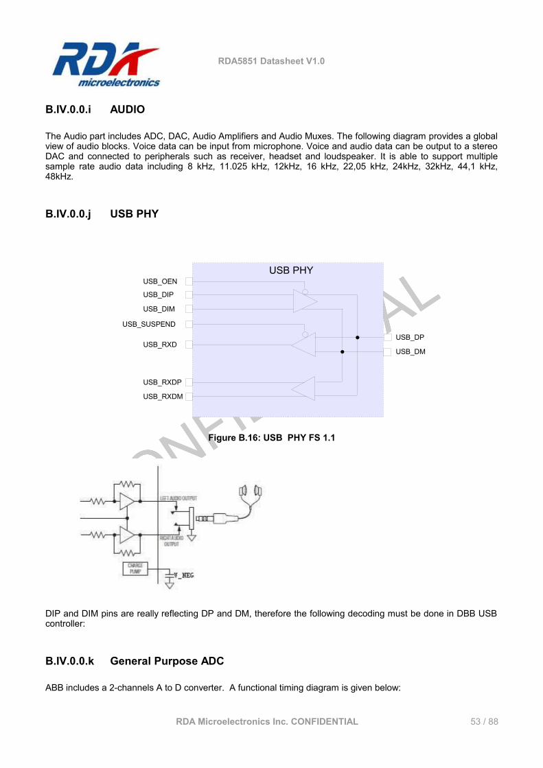
RDA5851 Datasheet V1.0
B.IV.0.0.i AUDIO
The Audio part includes ADC, DAC, Audio Amplifiers and Audio Muxes. The following diagram provides a global view of audio blocks. Voice data can be input from microphone. Voice and audio data can be output to a stereo DAC and connected to peripherals such as receiver, headset and loudspeaker. It is able to support multiple sample rate audio data including 8 kHz, 11.025 kHz, 12kHz, 16 kHz, 22,05 kHz, 24kHz, 32kHz, 44,1 kHz, 48kHz.
B.IV.0.0.j USB PHY
Figure B.16: USB PHY FS 1.1
DIP and DIM pins are really reflecting DP and DM, therefore the following decoding must be done in DBB USB controller:
B.IV.0.0.k General Purpose ADC
ABB includes a 2-channels A to D converter. A functional timing diagram is given below:
RDA Microelectronics Inc. CONFIDENTIAL 53 / 88
USB_OEN
USB_DIP
USB_DIM
USB_SUSPEND
USB_RXD
USB_RXDP
USB_RXDM
USB_DP
USB_DM
USB PHY
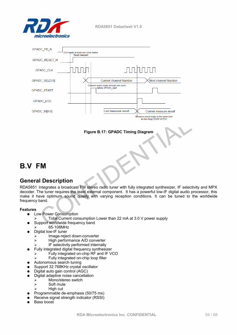
RDA5851 Datasheet V1.0
Figure B.17: GPADC Timing Diagram
B.V FM
General DescriptionRDA5851 Integrates a broadcast FM stereo radio tuner with fully integrated synthesizer, IF selectivity and MPX decoder. The tuner requires the least external component. It has a powerful low-IF digital audio processor, this make it have optimum sound quality with varying reception conditions. It can be tuned to the worldwide frequency band.
Features● Low Power Consumption
➢ Total Current consumption Lower than 22 mA at 3.0 V power supply● Support worldwide frequency band
➢ 65-108MHz● Digital low-IF tuner
➢ Image-reject down-converter➢ High performance A/D converter➢ IF selectivity performed internally
● Fully integrated digital frequency synthesizer➢ Fully integrated on-chip RF and IF VCO➢ Fully integrated on-chip loop filter
● Autonomous search tuning● Support 32.768KHz crystal oscillator● Digital auto gain control (AGC)● Digital adaptive noise cancellation
➢ Mono/stereo switch➢ Soft mute➢ High cut
● Programmable de-emphasis (50/75 ms)● Receive signal strength indicator (RSSI)● Bass boost
RDA Microelectronics Inc. CONFIDENTIAL 54 / 88
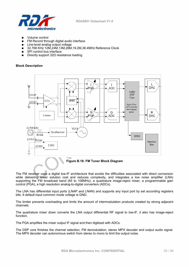
RDA5851 Datasheet V1.0
● Volume control● FM Record through digital audio interface● Line-level analog output voltage● 32.768 KHz 12M,24M,13M,26M,19.2M,38.4MHz Reference Clock● SPI control bus interface● Directly support 32Ω resistance loading
Block Description
The FM receiver uses a digital low-IF architecture that avoids the difficulties associated with direct conversion while delivering lower solution cost and reduces complexity, and integrates a low noise amplifier (LNA) supporting the FM broadcast band (65 to 108MHz), a quadrature image-reject mixer, a programmable gain control (PGA), a high resolution analog-to-digital converters (ADCs).
The LNA has differential input ports (LNAP and LNAN) and supports any input port by set according registers bits. It default input common mode voltage is GND.
The limiter prevents overloading and limits the amount of intermodulation products created by strong adjacent channels.
The quadrature mixer down converts the LNA output differential RF signal to low-IF, it also has image-reject function.
The PGA amplifies the mixer output IF signal and then digitized with ADCs.
The DSP core finishes the channel selection, FM demodulation, stereo MPX decoder and output audio signal. The MPX decoder can autonomous switch from stereo to mono to limit the output noise.
RDA Microelectronics Inc. CONFIDENTIAL 55 / 88
Figure B.18: FM Tuner Block Diagram
RDA5851 Datasheet V1.0
The frequency synthesizer generates the local oscillator signal which divide to quadrature, then be used to down-convert the RF input to a constant low intermediate frequency (IF). The synthesizer reference clock is 32.768 kHz. The synthesizer frequency is defined by register bits with the range from 65MHz to 108MHz.
Receiver Characteristics
(VDD = 2,7 to 5,5V, TA = -25°C to 85 °C, unless otherwise specified)
SYMBOL PARAMETER CONDITIONS MIN TYP MAX UNITGeneral Parameters
Fin FM Input FrequencyBAND=00 87 108 MHzBAND=01 76 91 MHzBAND=02 76 106 MHzBAND=03 65 76 MHz
Vrf Sensitivity1,2,3 (S+N)/N=26dB 1 1.5 µV EMFRin LNA Input Resistance7 150 ΩCin LNA Input Capacitance7 2 4 6 pFIP3in Input IP34 AGCD=1 80 - dBµV
aamAM Suppression1,2 M=0.3 40 - dB
S200 Adjacent Channel Selectivity ± 200kHz 45 - dBVAFL;VAFL Left and Right Audio
Frequency output Voltage Volume [3:0]=1111 200 mV
(S+N)/N Maximum Signal Plus Noise to Noise Ratio 1,2
55 60 - dB
aSCSStereo Channel Separation 35 - - dB
THD Audio Total Harmonic Distortion1,3,6
0.03 0.05 %
aAOIAudio Output L/R Imbalance 0.1 dB
RL Audio Output Loading Resistance
Single-ended 32 - - Ω
Pins LNAN, LNAPVcom_rfin Pins LNAN and LNAP Input
Common Mode Voltage0 V
Vcom Audio Output Common Mode Voltage
0.95 1 1.05 V
Notes:1. Fin=65 to 108MHz, Fmod=1KHz, de-emphasis=75µS,MONO=1;L=R unless noted otherwise.2. Δf =22.5KHz.3. BA =300Hz to 15KHz, RBW <= 10Hz.4. | f2-f1|>1MHz, f0=2xf1-f2, AGC disable, Fin=76 to 108MHz.5. PRF=60dbµV.6. Δf =75KHz.7. Measured at VEMF=1mV, FRF=65 to 108MHz.
RDA Microelectronics Inc. CONFIDENTIAL 56 / 88
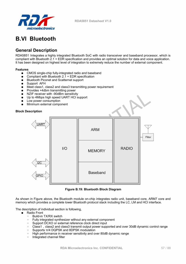
RDA5851 Datasheet V1.0
B.VI Bluetooth
General DescriptionRDA5851 Integrates a highly integrated Bluetooth SoC with radio transceiver and baseband processor, which is compliant with Bluetooth 2.1 + EDR specification and provides an optimal solution for data and voice application.It has been designed on highest level of integration to extremely reduce the number of external component.
Features● CMOS single-chip fully-integrated radio and baseband● Compliant with Bluetooth 2.1 + EDR specification● Bluetooth Piconet and Scatternet support● Support AFH● Meet class1, class2 and class3 transmitting power requirement● Provides +4dbm transmitting power● NZIF receiver with -90dBm sensitivity● Up to 4Mbps high speed UART HCI support● Low power consumption● Minimum external component
Block Description
As shown in Figure above, the Bluetooth module on-chip integrates radio unit, baseband core, ARM7 core and memory which provides a complete lower Bluetooth protocol stack including the LC, LM and HCI interface.
The description of individual section is following,● Radio Front
◦ Build-in TX/RX switch◦ Fully integrated synthesizer without any external component◦ Support DCXO or external reference clock direct input ◦ Class1,class2 and class3 transmit output power supported and over 30dB dynamic control range◦ Supports π/4 DQPSK and 8DPSK modulation◦ High performance in receiver sensitivity and over 80dB dynamic range◦ Integrated channel filter
RDA Microelectronics Inc. CONFIDENTIAL 57 / 88
Figure B.19: Bluetooth Block Diagram
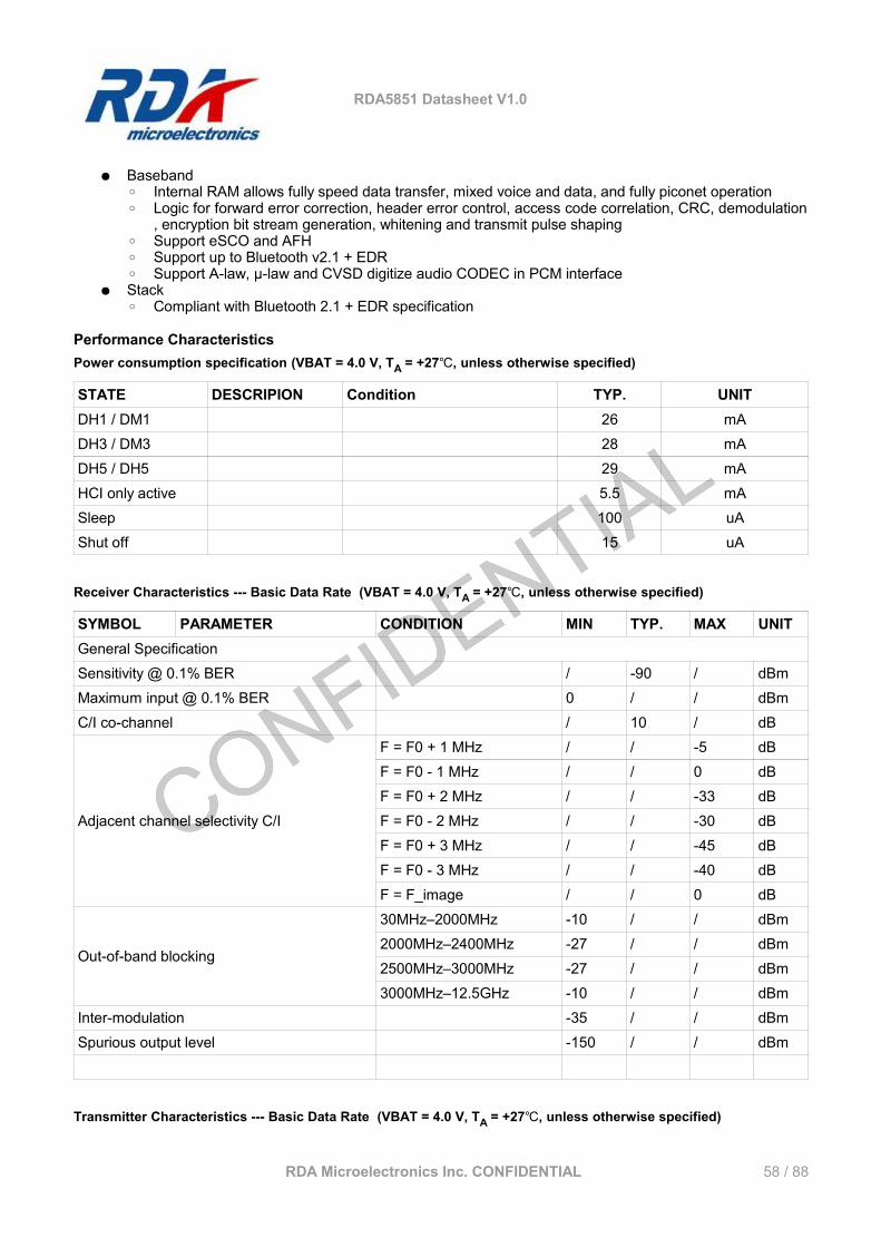
RDA5851 Datasheet V1.0
● Baseband◦ Internal RAM allows fully speed data transfer, mixed voice and data, and fully piconet operation◦ Logic for forward error correction, header error control, access code correlation, CRC, demodulation
, encryption bit stream generation, whitening and transmit pulse shaping◦ Support eSCO and AFH◦ Support up to Bluetooth v2.1 + EDR◦ Support A-law, μ-law and CVSD digitize audio CODEC in PCM interface
● Stack◦ Compliant with Bluetooth 2.1 + EDR specification
Performance CharacteristicsPower consumption specification (VBAT = 4.0 V, TA = +27 , unless otherwise specified)℃
STATE DESCRIPION Condition TYP. UNITDH1 / DM1 26 mADH3 / DM3 28 mADH5 / DH5 29 mAHCI only active 5.5 mASleep 100 uAShut off 15 uA
Receiver Characteristics --- Basic Data Rate (VBAT = 4.0 V, TA = +27 , unless otherwise specified)℃
SYMBOL PARAMETER CONDITION MIN TYP. MAX UNITGeneral SpecificationSensitivity @ 0.1% BER / -90 / dBmMaximum input @ 0.1% BER 0 / / dBmC/I co-channel / 10 / dB
Adjacent channel selectivity C/I
F = F0 + 1 MHz / / -5 dBF = F0 - 1 MHz / / 0 dBF = F0 + 2 MHz / / -33 dBF = F0 - 2 MHz / / -30 dBF = F0 + 3 MHz / / -45 dBF = F0 - 3 MHz / / -40 dBF = F_image / / 0 dB
Out-of-band blocking
30MHz–2000MHz -10 / / dBm2000MHz–2400MHz -27 / / dBm2500MHz–3000MHz -27 / / dBm3000MHz–12.5GHz -10 / / dBm
Inter-modulation -35 / / dBmSpurious output level -150 / / dBm
Transmitter Characteristics --- Basic Data Rate (VBAT = 4.0 V, TA = +27 , unless otherwise specified)℃
RDA Microelectronics Inc. CONFIDENTIAL 58 / 88
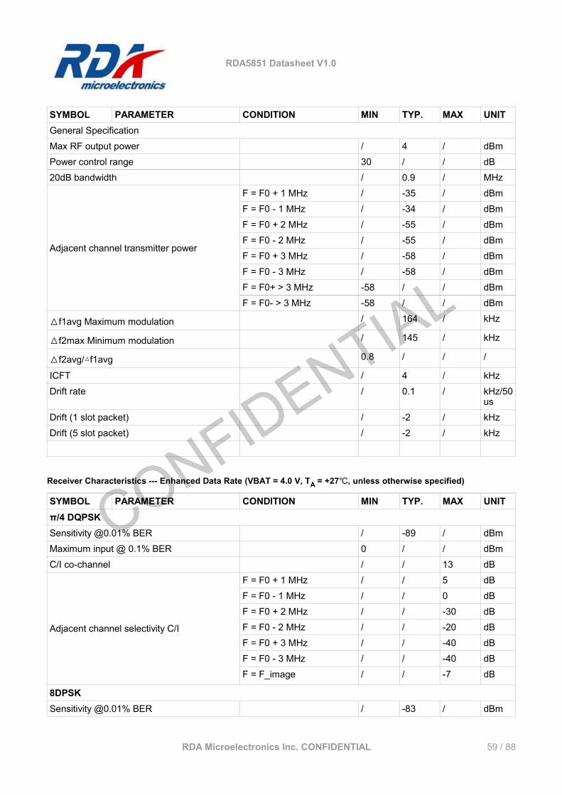
RDA5851 Datasheet V1.0
SYMBOL PARAMETER CONDITION MIN TYP. MAX UNITGeneral SpecificationMax RF output power / 4 / dBmPower control range 30 / / dB20dB bandwidth / 0.9 / MHz
Adjacent channel transmitter power
F = F0 + 1 MHz / -35 / dBmF = F0 - 1 MHz / -34 / dBmF = F0 + 2 MHz / -55 / dBmF = F0 - 2 MHz / -55 / dBmF = F0 + 3 MHz / -58 / dBmF = F0 - 3 MHz / -58 / dBmF = F0+ > 3 MHz -58 / / dBmF = F0- > 3 MHz -58 / / dBm
△f1avg Maximum modulation / 164 / kHz
△f2max Minimum modulation / 145 / kHz
△f2avg/ f1avg△ 0.8 / / /
ICFT / 4 / kHzDrift rate / 0.1 / kHz/50
usDrift (1 slot packet) / -2 / kHzDrift (5 slot packet) / -2 / kHz
Receiver Characteristics --- Enhanced Data Rate (VBAT = 4.0 V, TA = +27 , unless otherwise specified)℃
SYMBOL PARAMETER CONDITION MIN TYP. MAX UNITπ/4 DQPSKSensitivity @0.01% BER / -89 / dBmMaximum input @ 0.1% BER 0 / / dBmC/I co-channel / / 13 dB
Adjacent channel selectivity C/I
F = F0 + 1 MHz / / 5 dBF = F0 - 1 MHz / / 0 dBF = F0 + 2 MHz / / -30 dBF = F0 - 2 MHz / / -20 dBF = F0 + 3 MHz / / -40 dBF = F0 - 3 MHz / / -40 dBF = F_image / / -7 dB
8DPSKSensitivity @0.01% BER / -83 / dBm
RDA Microelectronics Inc. CONFIDENTIAL 59 / 88
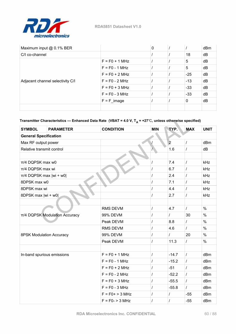
RDA5851 Datasheet V1.0
Maximum input @ 0.1% BER 0 / / dBmC/I co-channel / / 18 dB
Adjacent channel selectivity C/I
F = F0 + 1 MHz / / 5 dBF = F0 - 1 MHz / / 5 dBF = F0 + 2 MHz / / -25 dBF = F0 - 2 MHz / / -13 dBF = F0 + 3 MHz / / -33 dBF = F0 - 3 MHz / / -33 dBF = F_image / / 0 dB
Transmitter Characteristics --- Enhanced Data Rate (VBAT = 4.0 V, TA = +27 , unless otherwise specified)℃
SYMBOL PARAMETER CONDITION MIN TYP. MAX UNITGeneral SpecificationMax RF output power / 2 / dBmRelative transmit control / 1.6 / dB
π/4 DQPSK max w0 / 7.4 / kHzπ/4 DQPSK max wi / 6.7 / kHzπ/4 DQPSK max |wi + w0| / 2.4 / kHz8DPSK max w0 / 7.1 / kHz8DPSK max wi / 4.4 / kHz8DPSK max |wi + w0| / 2.7 / kHz
π/4 DQPSK Modulation AccuracyRMS DEVM / 4.7 / %99% DEVM / / 30 %Peak DEVM / 8.8 / %
8PSK Modulation AccuracyRMS DEVM / 4.6 / %99% DEVM / / 20 %Peak DEVM / 11.3 / %
In-band spurious emissions F = F0 + 1 MHz / -14.7 / dBmF = F0 - 1 MHz / -15.2 / dBmF = F0 + 2 MHz / -51 / dBmF = F0 - 2 MHz / -52.2 / dBmF = F0 + 3 MHz / -55.5 / dBmF = F0 - 3 MHz / -55.8 / dBmF = F0+ > 3 MHz / / -55 dBmF = F0- > 3 MHz / / -55 dBm
RDA Microelectronics Inc. CONFIDENTIAL 60 / 88
RDA5851 Datasheet V1.0
EDR Differential Phase Coding / 100 / %
RDA Microelectronics Inc. CONFIDENTIAL 61 / 88
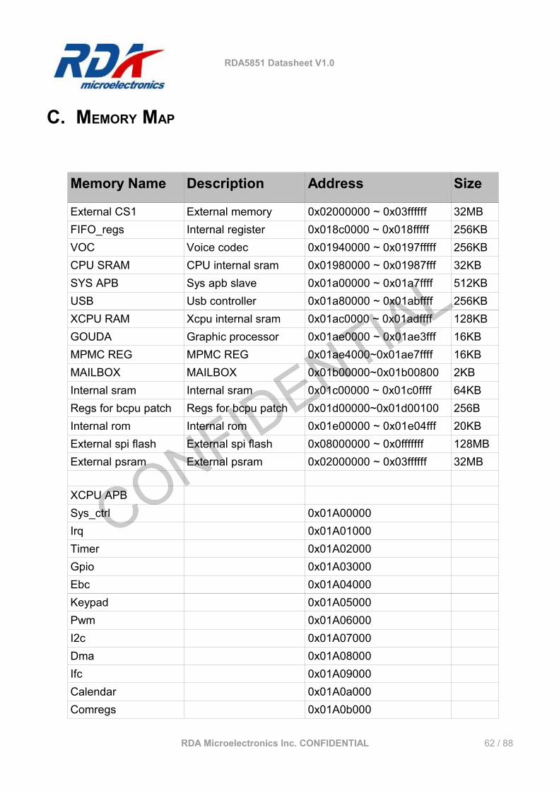
RDA5851 Datasheet V1.0
C. MEMORY MAP
Memory Name Description Address Size
External CS1 External memory 0x02000000 ~ 0x03ffffff 32MBFIFO_regs Internal register 0x018c0000 ~ 0x018fffff 256KBVOC Voice codec 0x01940000 ~ 0x0197fffff 256KBCPU SRAM CPU internal sram 0x01980000 ~ 0x01987fff 32KBSYS APB Sys apb slave 0x01a00000 ~ 0x01a7ffff 512KBUSB Usb controller 0x01a80000 ~ 0x01abffff 256KBXCPU RAM Xcpu internal sram 0x01ac0000 ~ 0x01adffff 128KBGOUDA Graphic processor 0x01ae0000 ~ 0x01ae3fff 16KBMPMC REG MPMC REG 0x01ae4000~0x01ae7ffff 16KBMAILBOX MAILBOX 0x01b00000~0x01b00800 2KBInternal sram Internal sram 0x01c00000 ~ 0x01c0ffff 64KBRegs for bcpu patch Regs for bcpu patch 0x01d00000~0x01d00100 256BInternal rom Internal rom 0x01e00000 ~ 0x01e04fff 20KBExternal spi flash External spi flash 0x08000000 ~ 0x0fffffff 128MBExternal psram External psram 0x02000000 ~ 0x03ffffff 32MB
XCPU APBSys_ctrl 0x01A00000Irq 0x01A01000Timer 0x01A02000Gpio 0x01A03000Ebc 0x01A04000Keypad 0x01A05000Pwm 0x01A06000I2c 0x01A07000Dma 0x01A08000Ifc 0x01A09000Calendar 0x01A0a000Comregs 0x01A0b000
RDA Microelectronics Inc. CONFIDENTIAL 62 / 88
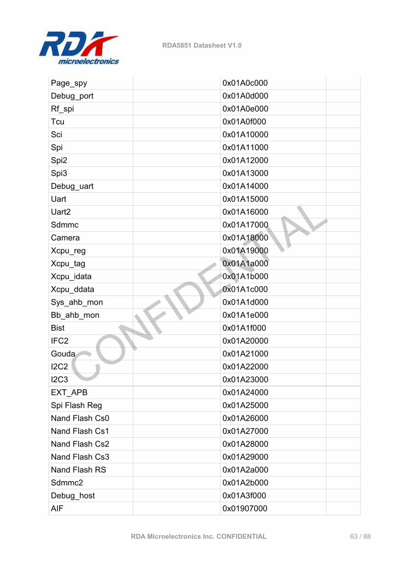
RDA5851 Datasheet V1.0
Page_spy 0x01A0c000Debug_port 0x01A0d000Rf_spi 0x01A0e000Tcu 0x01A0f000Sci 0x01A10000Spi 0x01A11000Spi2 0x01A12000Spi3 0x01A13000Debug_uart 0x01A14000Uart 0x01A15000Uart2 0x01A16000Sdmmc 0x01A17000Camera 0x01A18000Xcpu_reg 0x01A19000Xcpu_tag 0x01A1a000Xcpu_idata 0x01A1b000Xcpu_ddata 0x01A1c000Sys_ahb_mon 0x01A1d000Bb_ahb_mon 0x01A1e000Bist 0x01A1f000IFC2 0x01A20000Gouda 0x01A21000I2C2 0x01A22000I2C3 0x01A23000EXT_APB 0x01A24000Spi Flash Reg 0x01A25000Nand Flash Cs0 0x01A26000Nand Flash Cs1 0x01A27000Nand Flash Cs2 0x01A28000Nand Flash Cs3 0x01A29000Nand Flash RS 0x01A2a000Sdmmc2 0x01A2b000Debug_host 0x01A3f000AIF 0x01907000
RDA Microelectronics Inc. CONFIDENTIAL 63 / 88
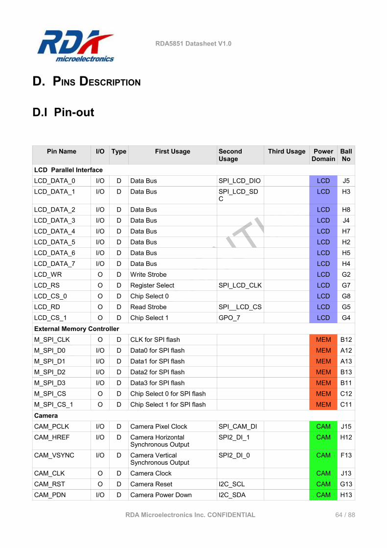
RDA5851 Datasheet V1.0
D. PINS DESCRIPTION
D.I Pin-out
Pin Name I/O Type First Usage Second Usage
Third Usage Power Domain
Ball No
LCD Parallel Interface LCD_DATA_0 I/O D Data Bus SPI_LCD_DIO LCD J5LCD_DATA_1 I/O D Data Bus SPI_LCD_SD
CLCD H3
LCD_DATA_2 I/O D Data Bus LCD H8LCD_DATA_3 I/O D Data Bus LCD J4LCD_DATA_4 I/O D Data Bus LCD H7LCD_DATA_5 I/O D Data Bus LCD H2LCD_DATA_6 I/O D Data Bus LCD H5LCD_DATA_7 I/O D Data Bus LCD H4LCD_WR O D Write Strobe LCD G2LCD_RS O D Register Select SPI_LCD_CLK LCD G7LCD_CS_0 O D Chip Select 0 LCD G8LCD_RD O D Read Strobe SPI__LCD_CS LCD G5LCD_CS_1 O D Chip Select 1 GPO_7 LCD G4
External Memory Controller M_SPI_CLK O D CLK for SPI flash MEM B12M_SPI_D0 I/O D Data0 for SPI flash MEM A12M_SPI_D1 I/O D Data1 for SPI flash MEM A13M_SPI_D2 I/O D Data2 for SPI flash MEM B13M_SPI_D3 I/O D Data3 for SPI flash MEM B11M_SPI_CS O D Chip Select 0 for SPI flash MEM C12M_SPI_CS_1 O D Chip Select 1 for SPI flash MEM C11
CameraCAM_PCLK I/O D Camera Pixel Clock SPI_CAM_DI CAM J15CAM_HREF I/O D Camera Horizontal
Synchronous OutputSPI2_DI_1 CAM H12
CAM_VSYNC I/O D Camera Vertical Synchronous Output
SPI2_DI_0 CAM F13
CAM_CLK O D Camera Clock CAM J13CAM_RST O D Camera Reset I2C_SCL CAM G13CAM_PDN I/O D Camera Power Down I2C_SDA CAM H13
RDA Microelectronics Inc. CONFIDENTIAL 64 / 88
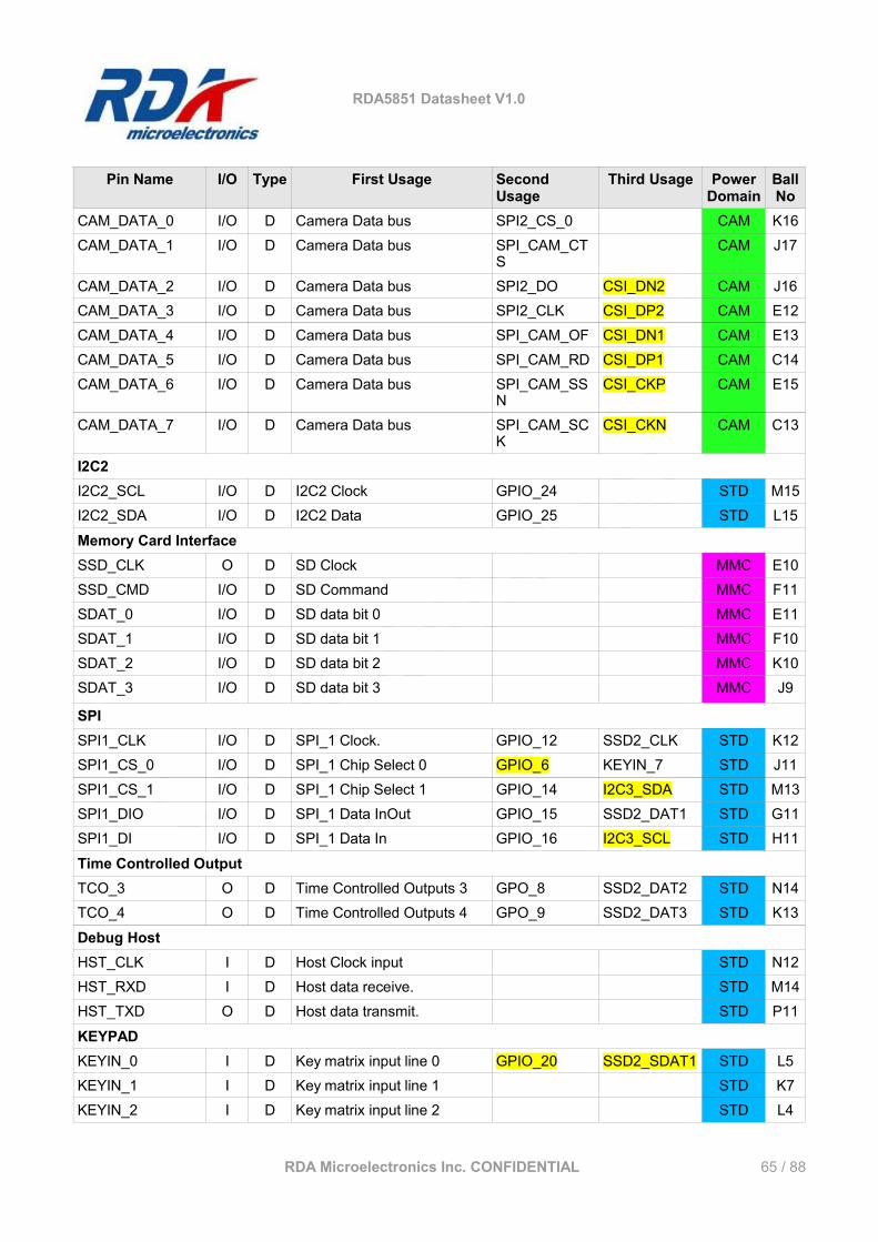
RDA5851 Datasheet V1.0
Pin Name I/O Type First Usage Second Usage
Third Usage Power Domain
Ball No
CAM_DATA_0 I/O D Camera Data bus SPI2_CS_0 CAM K16CAM_DATA_1 I/O D Camera Data bus SPI_CAM_CT
SCAM J17
CAM_DATA_2 I/O D Camera Data bus SPI2_DO CSI_DN2 CAM J16CAM_DATA_3 I/O D Camera Data bus SPI2_CLK CSI_DP2 CAM E12CAM_DATA_4 I/O D Camera Data bus SPI_CAM_OF CSI_DN1 CAM E13CAM_DATA_5 I/O D Camera Data bus SPI_CAM_RD CSI_DP1 CAM C14CAM_DATA_6 I/O D Camera Data bus SPI_CAM_SS
NCSI_CKP CAM E15
CAM_DATA_7 I/O D Camera Data bus SPI_CAM_SCK
CSI_CKN CAM C13
I2C2 I2C2_SCL I/O D I2C2 Clock GPIO_24 STD M15I2C2_SDA I/O D I2C2 Data GPIO_25 STD L15
Memory Card Interface SSD_CLK O D SD Clock MMC E10SSD_CMD I/O D SD Command MMC F11SDAT_0 I/O D SD data bit 0 MMC E11SDAT_1 I/O D SD data bit 1 MMC F10SDAT_2 I/O D SD data bit 2 MMC K10SDAT_3 I/O D SD data bit 3 MMC J9
SPI SPI1_CLK I/O D SPI_1 Clock. GPIO_12 SSD2_CLK STD K12SPI1_CS_0 I/O D SPI_1 Chip Select 0 GPIO_6 KEYIN_7 STD J11SPI1_CS_1 I/O D SPI_1 Chip Select 1 GPIO_14 I2C3_SDA STD M13SPI1_DIO I/O D SPI_1 Data InOut GPIO_15 SSD2_DAT1 STD G11SPI1_DI I/O D SPI_1 Data In GPIO_16 I2C3_SCL STD H11
Time Controlled Output TCO_3 O D Time Controlled Outputs 3 GPO_8 SSD2_DAT2 STD N14TCO_4 O D Time Controlled Outputs 4 GPO_9 SSD2_DAT3 STD K13
Debug Host HST_CLK I D Host Clock input STD N12HST_RXD I D Host data receive. STD M14HST_TXD O D Host data transmit. STD P11
KEYPAD KEYIN_0 I D Key matrix input line 0 GPIO_20 SSD2_SDAT1 STD L5KEYIN_1 I D Key matrix input line 1 STD K7KEYIN_2 I D Key matrix input line 2 STD L4
RDA Microelectronics Inc. CONFIDENTIAL 65 / 88
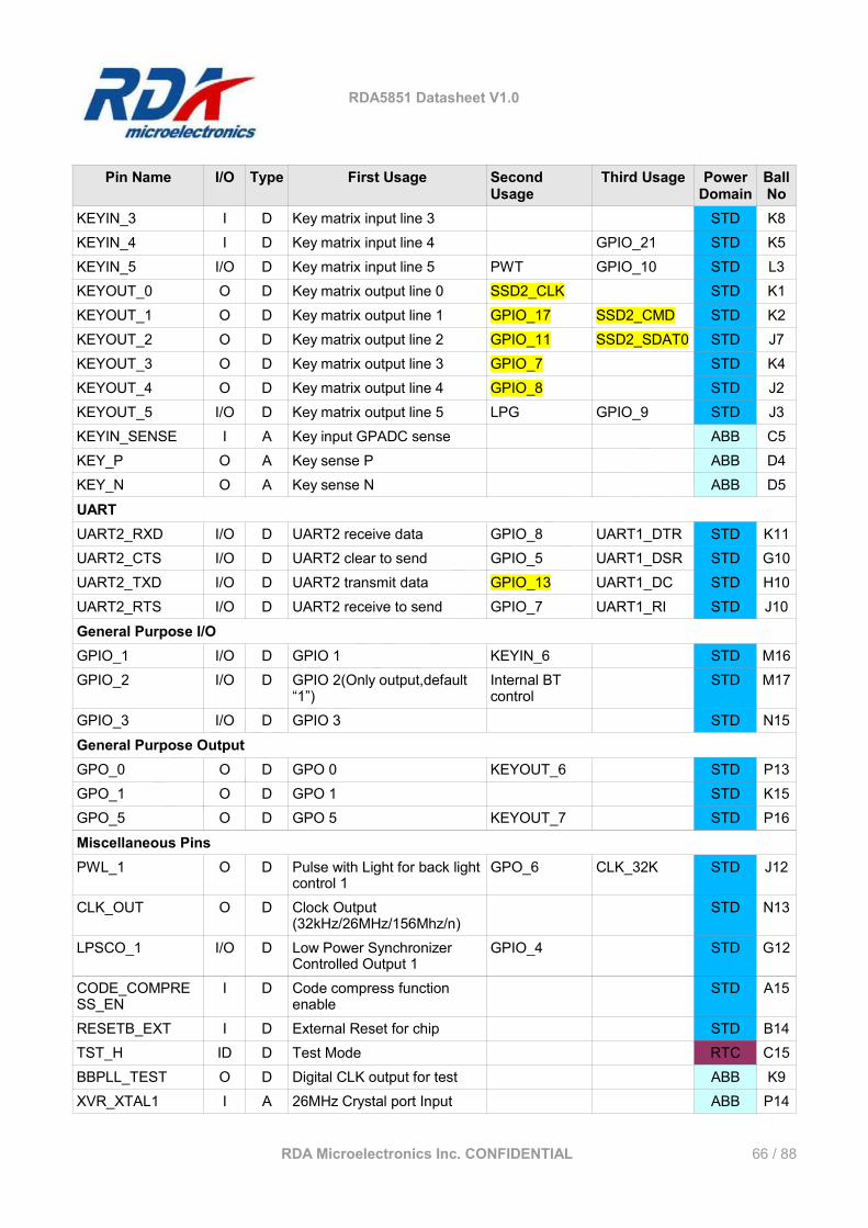
RDA5851 Datasheet V1.0
Pin Name I/O Type First Usage Second Usage
Third Usage Power Domain
Ball No
KEYIN_3 I D Key matrix input line 3 STD K8KEYIN_4 I D Key matrix input line 4 GPIO_21 STD K5KEYIN_5 I/O D Key matrix input line 5 PWT GPIO_10 STD L3KEYOUT_0 O D Key matrix output line 0 SSD2_CLK STD K1KEYOUT_1 O D Key matrix output line 1 GPIO_17 SSD2_CMD STD K2KEYOUT_2 O D Key matrix output line 2 GPIO_11 SSD2_SDAT0 STD J7KEYOUT_3 O D Key matrix output line 3 GPIO_7 STD K4KEYOUT_4 O D Key matrix output line 4 GPIO_8 STD J2KEYOUT_5 I/O D Key matrix output line 5 LPG GPIO_9 STD J3KEYIN_SENSE I A Key input GPADC sense ABB C5KEY_P O A Key sense P ABB D4KEY_N O A Key sense N ABB D5
UARTUART2_RXD I/O D UART2 receive data GPIO_8 UART1_DTR STD K11UART2_CTS I/O D UART2 clear to send GPIO_5 UART1_DSR STD G10UART2_TXD I/O D UART2 transmit data GPIO_13 UART1_DC STD H10UART2_RTS I/O D UART2 receive to send GPIO_7 UART1_RI STD J10
General Purpose I/O GPIO_1 I/O D GPIO 1 KEYIN_6 STD M16GPIO_2 I/O D GPIO 2(Only output,default
“1”)Internal BT control
STD M17
GPIO_3 I/O D GPIO 3 STD N15
General Purpose Output GPO_0 O D GPO 0 KEYOUT_6 STD P13GPO_1 O D GPO 1 STD K15GPO_5 O D GPO 5 KEYOUT_7 STD P16
Miscellaneous Pins PWL_1 O D Pulse with Light for back light
control 1GPO_6 CLK_32K STD J12
CLK_OUT O D Clock Output (32kHz/26MHz/156Mhz/n)
STD N13
LPSCO_1 I/O D Low Power Synchronizer Controlled Output 1
GPIO_4 STD G12
CODE_COMPRESS_EN
I D Code compress function enable
STD A15
RESETB_EXT I D External Reset for chip STD B14TST_H ID D Test Mode RTC C15BBPLL_TEST O D Digital CLK output for test ABB K9XVR_XTAL1 I A 26MHz Crystal port Input ABB P14
RDA Microelectronics Inc. CONFIDENTIAL 66 / 88
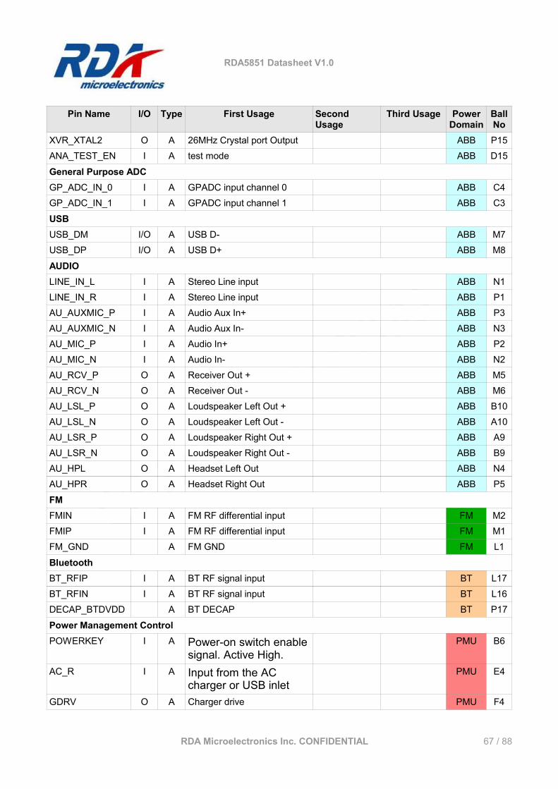
RDA5851 Datasheet V1.0
Pin Name I/O Type First Usage Second Usage
Third Usage Power Domain
Ball No
XVR_XTAL2 O A 26MHz Crystal port Output ABB P15ANA_TEST_EN I A test mode ABB D15
General Purpose ADC GP_ADC_IN_0 I A GPADC input channel 0 ABB C4GP_ADC_IN_1 I A GPADC input channel 1 ABB C3
USB USB_DM I/O A USB D- ABB M7USB_DP I/O A USB D+ ABB M8
AUDIO LINE_IN_L I A Stereo Line input ABB N1LINE_IN_R I A Stereo Line input ABB P1AU_AUXMIC_P I A Audio Aux In+ ABB P3AU_AUXMIC_N I A Audio Aux In- ABB N3AU_MIC_P I A Audio In+ ABB P2AU_MIC_N I A Audio In- ABB N2AU_RCV_P O A Receiver Out + ABB M5AU_RCV_N O A Receiver Out - ABB M6AU_LSL_P O A Loudspeaker Left Out + ABB B10AU_LSL_N O A Loudspeaker Left Out - ABB A10AU_LSR_P O A Loudspeaker Right Out + ABB A9AU_LSR_N O A Loudspeaker Right Out - ABB B9AU_HPL O A Headset Left Out ABB N4AU_HPR O A Headset Right Out ABB P5
FMFMIN I A FM RF differential input FM M2FMIP I A FM RF differential input FM M1FM_GND A FM GND FM L1
BluetoothBT_RFIP I A BT RF signal input BT L17BT_RFIN I A BT RF signal input BT L16DECAP_BTDVDD A BT DECAP BT P17
Power Management Control POWERKEY I A Power-on switch enable
signal. Active High.PMU B6
AC_R I A Input from the AC charger or USB inlet
PMU E4
GDRV O A Charger drive PMU F4
RDA Microelectronics Inc. CONFIDENTIAL 67 / 88
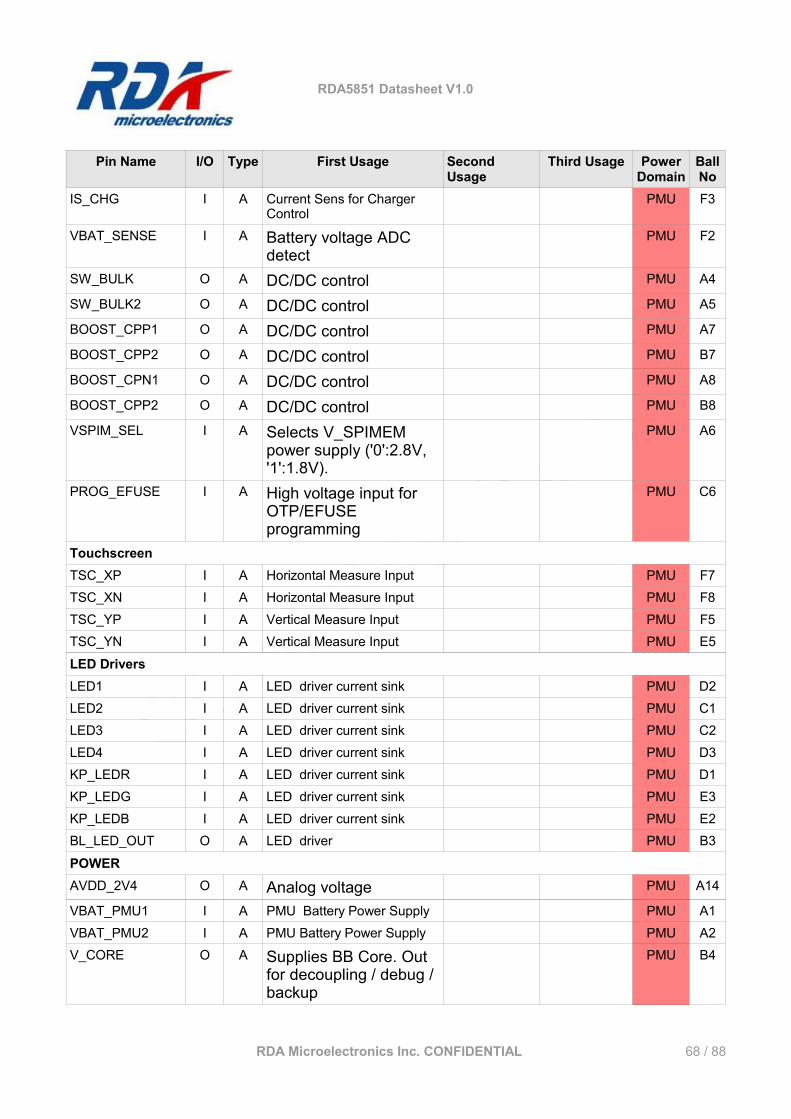
RDA5851 Datasheet V1.0
Pin Name I/O Type First Usage Second Usage
Third Usage Power Domain
Ball No
IS_CHG I A Current Sens for Charger Control
PMU F3
VBAT_SENSE I A Battery voltage ADC detect
PMU F2
SW_BULK O A DC/DC control PMU A4
SW_BULK2 O A DC/DC control PMU A5
BOOST_CPP1 O A DC/DC control PMU A7
BOOST_CPP2 O A DC/DC control PMU B7
BOOST_CPN1 O A DC/DC control PMU A8
BOOST_CPP2 O A DC/DC control PMU B8
VSPIM_SEL I A Selects V_SPIMEM power supply ('0':2.8V, '1':1.8V).
PMU A6
PROG_EFUSE I A High voltage input for OTP/EFUSE programming
PMU C6
Touchscreen TSC_XP I A Horizontal Measure Input PMU F7TSC_XN I A Horizontal Measure Input PMU F8TSC_YP I A Vertical Measure Input PMU F5TSC_YN I A Vertical Measure Input PMU E5
LED Drivers LED1 I A LED driver current sink PMU D2LED2 I A LED driver current sink PMU C1LED3 I A LED driver current sink PMU C2LED4 I A LED driver current sink PMU D3KP_LEDR I A LED driver current sink PMU D1KP_LEDG I A LED driver current sink PMU E3KP_LEDB I A LED driver current sink PMU E2BL_LED_OUT O A LED driver PMU B3
POWER AVDD_2V4 O A Analog voltage PMU A14
VBAT_PMU1 I A PMU Battery Power Supply PMU A1VBAT_PMU2 I A PMU Battery Power Supply PMU A2V_CORE O A Supplies BB Core. Out
for decoupling / debug / backup
PMU B4
RDA Microelectronics Inc. CONFIDENTIAL 68 / 88
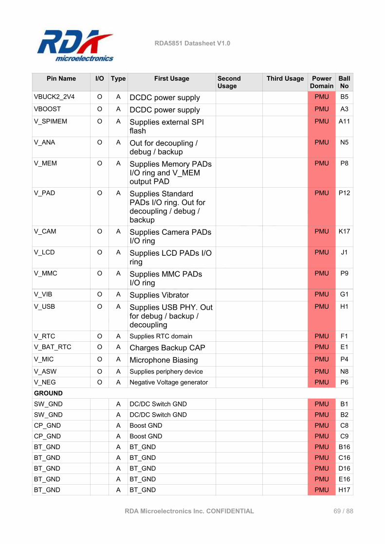
RDA5851 Datasheet V1.0
Pin Name I/O Type First Usage Second Usage
Third Usage Power Domain
Ball No
VBUCK2_2V4 O A DCDC power supply PMU B5
VBOOST O A DCDC power supply PMU A3
V_SPIMEM O A Supplies external SPI flash
PMU A11
V_ANA O A Out for decoupling / debug / backup
PMU N5
V_MEM O A Supplies Memory PADs I/O ring and V_MEM output PAD
PMU P8
V_PAD O A Supplies Standard PADs I/O ring. Out for decoupling / debug / backup
PMU P12
V_CAM O A Supplies Camera PADs I/O ring
PMU K17
V_LCD O A Supplies LCD PADs I/O ring
PMU J1
V_MMC O A Supplies MMC PADs I/O ring
PMU P9
V_VIB O A Supplies Vibrator PMU G1
V_USB O A Supplies USB PHY. Out for debug / backup / decoupling
PMU H1
V_RTC O A Supplies RTC domain PMU F1V_BAT_RTC O A Charges Backup CAP PMU E1
V_MIC O A Microphone Biasing PMU P4
V_ASW O A Supplies periphery device PMU N8V_NEG O A Negative Voltage generator PMU P6
GROUND SW_GND A DC/DC Switch GND PMU B1SW_GND A DC/DC Switch GND PMU B2CP_GND A Boost GND PMU C8CP_GND A Boost GND PMU C9BT_GND A BT_GND PMU B16BT_GND A BT_GND PMU C16BT_GND A BT_GND PMU D16BT_GND A BT_GND PMU E16BT_GND A BT_GND PMU H17
RDA Microelectronics Inc. CONFIDENTIAL 69 / 88
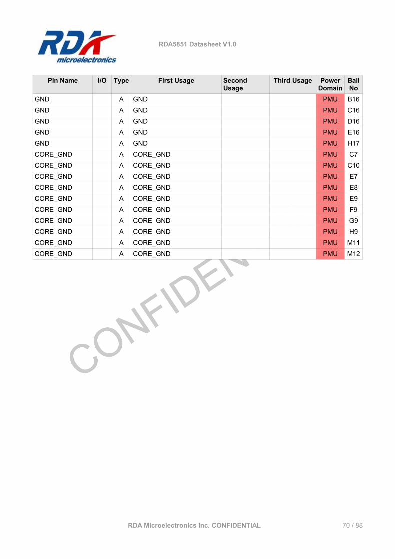
RDA5851 Datasheet V1.0
Pin Name I/O Type First Usage Second Usage
Third Usage Power Domain
Ball No
GND A GND PMU B16GND A GND PMU C16GND A GND PMU D16GND A GND PMU E16GND A GND PMU H17CORE_GND A CORE_GND PMU C7CORE_GND A CORE_GND PMU C10CORE_GND A CORE_GND PMU E7CORE_GND A CORE_GND PMU E8CORE_GND A CORE_GND PMU E9CORE_GND A CORE_GND PMU F9CORE_GND A CORE_GND PMU G9CORE_GND A CORE_GND PMU H9CORE_GND A CORE_GND PMU M11CORE_GND A CORE_GND PMU M12
RDA Microelectronics Inc. CONFIDENTIAL 70 / 88
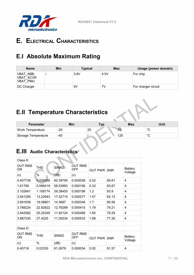
RDA5851 Datasheet V1.0
E. ELECTRICAL CHARACTERISTICS
E.I Absolute Maximum Rating
Name Min Typical Max Usage (power domain)VBAT_ABB,VBAT_XCVRVBAT_PMU
/ 3.8V 4.5V For chip
DC Charger 5V 7V For charger circuit
E.II Temperature Characteristics
Parameter Min Typ Max UnitWork Temperature -25 25 70 °C
Storage Temperature -40 / 125 °C
E.III Audio Characteristics
Class K
OUT RMS ON THD SINAD OUT RMS
OFF OUT PWR SNR Battery Voltage
(v) % (dB) (v)0.407738 0.028088 60.39795 0.000038 0.02 80.61 41.61769 0.089419 58.53993 0.000106 0.33 83.67 43.102641 1.108774 38.38455 0.000198 1.2 83.9 43.541256 13.22943 17.52715 0.000277 1.57 82.13 43.691639 19.08801 14.3687 0.000346 1.7 80.56 43.788224 22.92822 12.76289 0.000415 1.79 79.21 43.842082 25.25349 11.92124 0.000468 1.85 78.29 43.887335 27.4225 11.20234 0.000533 1.89 77.26 4
Class D
OUT RMS ON THD SINAD OUT RMS
OFF OUT PWR SNR Battery Voltage
(v) % (dB) (v)0.40716 0.02335 61.2679 0.000034 0.02 81.57 4
RDA Microelectronics Inc. CONFIDENTIAL 71 / 88
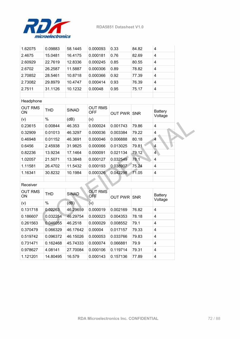
RDA5851 Datasheet V1.0
1.62075 0.09883 58.1445 0.000093 0.33 84.82 42.4675 15.0481 16.4175 0.000181 0.76 82.69 42.60929 22.7619 12.8336 0.000245 0.85 80.55 42.6702 26.2587 11.5887 0.000306 0.89 78.82 42.70852 28.5461 10.8718 0.000366 0.92 77.39 42.73082 29.8979 10.4747 0.000414 0.93 76.39 42.7511 31.1126 10.1232 0.00048 0.95 75.17 4
Headphone
OUT RMS ON THD SINAD OUT RMS
OFF OUT PWR SNR Battery Voltage
(v) % (dB) (v)0.23615 0.00844 46.353 0.000024 0.001743 79.86 40.32909 0.01013 46.3297 0.000036 0.003384 79.22 40.46948 0.01152 46.3691 0.000046 0.006888 80.18 40.6456 2.45938 31.9825 0.000066 0.013025 79.81 40.82236 13.9234 17.1464 0.000091 0.021134 79.12 41.02057 21.5071 13.3848 0.000127 0.032549 78.1 41.11581 26.4702 11.5432 0.000193 0.038907 75.24 41.16341 30.8232 10.1984 0.000326 0.042298 71.05 4
Receiver
OUT RMS ON THD SINAD OUT RMS
OFF OUT PWR SNR Battery Voltage
(v) % (dB) (v)0.131718 0.02263 46.29659 0.000019 0.002169 76.82 40.186607 0.032254 46.29754 0.000023 0.004353 78.18 40.261563 0.046055 46.2518 0.000029 0.008552 79.1 40.370479 0.066329 46.17642 0.00004 0.017157 79.33 40.519742 0.096372 46.15026 0.000053 0.033766 79.83 40.731471 0.162468 45.74333 0.000074 0.066881 79.9 40.978627 4.08141 27.70084 0.000106 0.119714 79.31 41.121201 14.80495 16.579 0.000143 0.157136 77.89 4
RDA Microelectronics Inc. CONFIDENTIAL 72 / 88
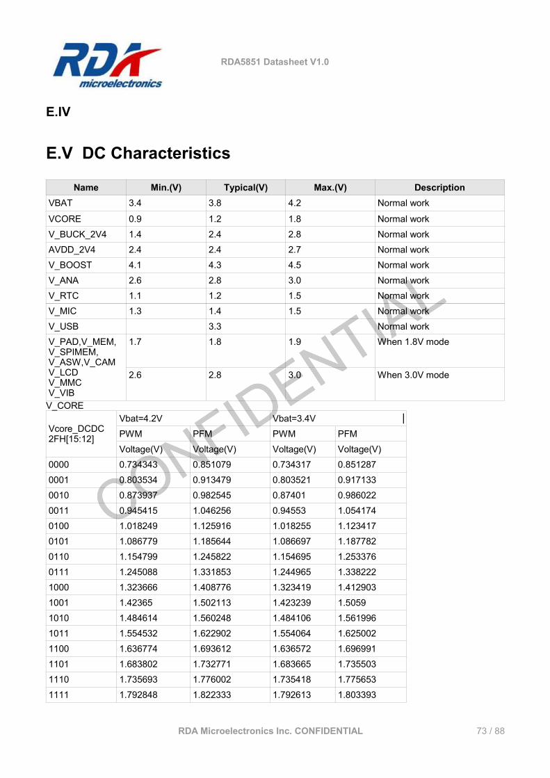
RDA5851 Datasheet V1.0
E.IV
E.V DC Characteristics
Name Min.(V) Typical(V) Max.(V) DescriptionVBAT 3.4 3.8 4.2 Normal work
VCORE 0.9 1.2 1.8 Normal workV_BUCK_2V4 1.4 2.4 2.8 Normal workAVDD_2V4 2.4 2.4 2.7 Normal workV_BOOST 4.1 4.3 4.5 Normal workV_ANA 2.6 2.8 3.0 Normal workV_RTC 1.1 1.2 1.5 Normal workV_MIC 1.3 1.4 1.5 Normal workV_USB 3.3 Normal workV_PAD,V_MEM,V_SPIMEM,V_ASW,V_CAMV_LCDV_MMCV_VIB
1.7 1.8 1.9 When 1.8V mode
2.6 2.8 3.0 When 3.0V mode
V_CORE
Vcore_DCDC2FH[15:12]
Vbat=4.2V Vbat=3.4VPWM PFM PWM PFMVoltage(V) Voltage(V) Voltage(V) Voltage(V)
0000 0.734343 0.851079 0.734317 0.8512870001 0.803534 0.913479 0.803521 0.9171330010 0.873937 0.982545 0.87401 0.9860220011 0.945415 1.046256 0.94553 1.0541740100 1.018249 1.125916 1.018255 1.1234170101 1.086779 1.185644 1.086697 1.1877820110 1.154799 1.245822 1.154695 1.2533760111 1.245088 1.331853 1.244965 1.3382221000 1.323666 1.408776 1.323419 1.4129031001 1.42365 1.502113 1.423239 1.50591010 1.484614 1.560248 1.484106 1.5619961011 1.554532 1.622902 1.554064 1.6250021100 1.636774 1.693612 1.636572 1.6969911101 1.683802 1.732771 1.683665 1.7355031110 1.735693 1.776002 1.735418 1.7756531111 1.792848 1.822333 1.792613 1.803393
RDA Microelectronics Inc. CONFIDENTIAL 73 / 88
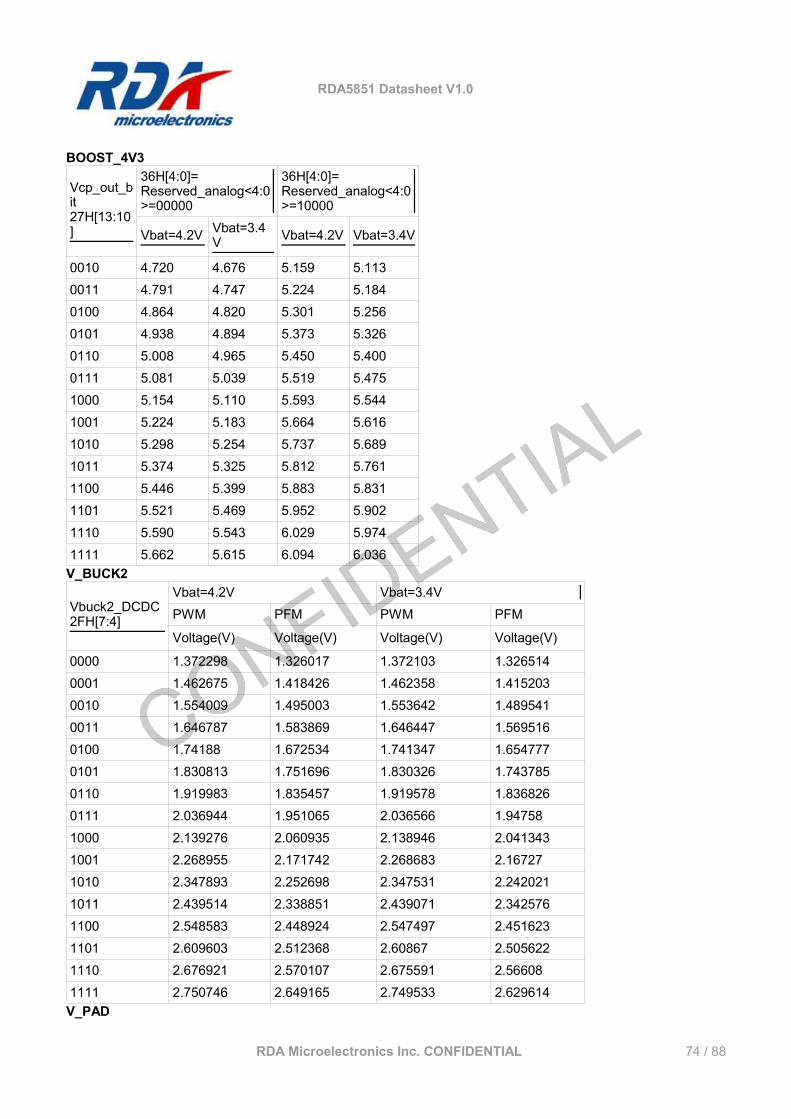
RDA5851 Datasheet V1.0
BOOST_4V3
Vcp_out_bit27H[13:10]
36H[4:0]=Reserved_analog<4:0>=00000
36H[4:0]=Reserved_analog<4:0>=10000
Vbat=4.2V Vbat=3.4V Vbat=4.2V Vbat=3.4V
0010 4.720 4.676 5.159 5.113 0011 4.791 4.747 5.224 5.184 0100 4.864 4.820 5.301 5.256 0101 4.938 4.894 5.373 5.326 0110 5.008 4.965 5.450 5.400 0111 5.081 5.039 5.519 5.475 1000 5.154 5.110 5.593 5.544 1001 5.224 5.183 5.664 5.616 1010 5.298 5.254 5.737 5.689 1011 5.374 5.325 5.812 5.761 1100 5.446 5.399 5.883 5.831 1101 5.521 5.469 5.952 5.902 1110 5.590 5.543 6.029 5.974 1111 5.662 5.615 6.094 6.036
V_BUCK2
Vbuck2_DCDC2FH[7:4]
Vbat=4.2V Vbat=3.4VPWM PFM PWM PFM
Voltage(V) Voltage(V) Voltage(V) Voltage(V)
0000 1.372298 1.326017 1.372103 1.3265140001 1.462675 1.418426 1.462358 1.4152030010 1.554009 1.495003 1.553642 1.4895410011 1.646787 1.583869 1.646447 1.5695160100 1.74188 1.672534 1.741347 1.6547770101 1.830813 1.751696 1.830326 1.7437850110 1.919983 1.835457 1.919578 1.8368260111 2.036944 1.951065 2.036566 1.947581000 2.139276 2.060935 2.138946 2.0413431001 2.268955 2.171742 2.268683 2.167271010 2.347893 2.252698 2.347531 2.2420211011 2.439514 2.338851 2.439071 2.3425761100 2.548583 2.448924 2.547497 2.4516231101 2.609603 2.512368 2.60867 2.5056221110 2.676921 2.570107 2.675591 2.566081111 2.750746 2.649165 2.749533 2.629614
V_PAD
RDA Microelectronics Inc. CONFIDENTIAL 74 / 88
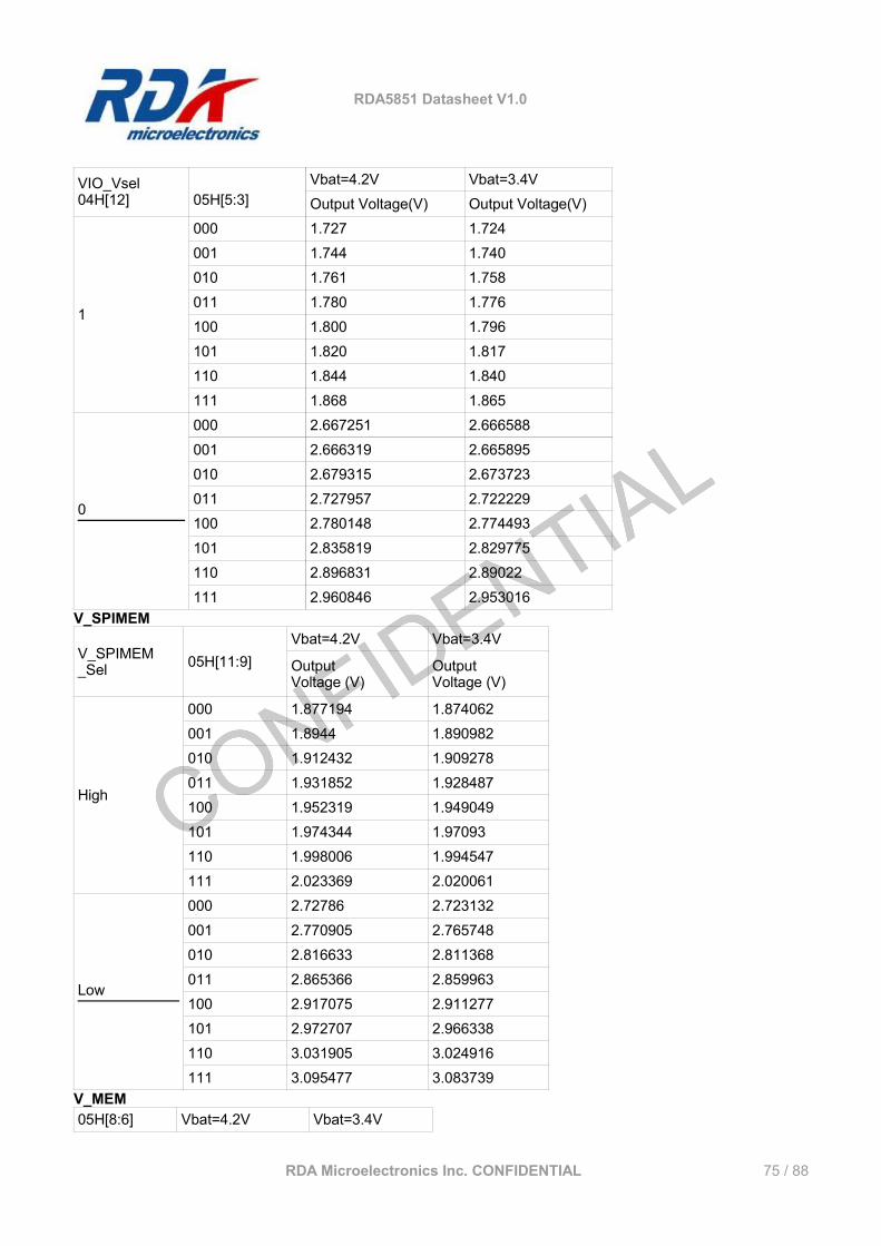
RDA5851 Datasheet V1.0
VIO_Vsel04H[12] 05H[5:3]
Vbat=4.2V Vbat=3.4VOutput Voltage(V) Output Voltage(V)
1
000 1.727 1.724 001 1.744 1.740 010 1.761 1.758 011 1.780 1.776 100 1.800 1.796 101 1.820 1.817 110 1.844 1.840 111 1.868 1.865
0
000 2.667251 2.666588001 2.666319 2.665895010 2.679315 2.673723011 2.727957 2.722229100 2.780148 2.774493101 2.835819 2.829775110 2.896831 2.89022111 2.960846 2.953016
V_SPIMEM
V_SPIMEM_Sel 05H[11:9]
Vbat=4.2V Vbat=3.4V
Output Voltage (V)
Output Voltage (V)
High
000 1.877194 1.874062001 1.8944 1.890982010 1.912432 1.909278011 1.931852 1.928487100 1.952319 1.949049101 1.974344 1.97093110 1.998006 1.994547111 2.023369 2.020061
Low
000 2.72786 2.723132001 2.770905 2.765748010 2.816633 2.811368011 2.865366 2.859963100 2.917075 2.911277101 2.972707 2.966338110 3.031905 3.024916111 3.095477 3.083739
V_MEM05H[8:6] Vbat=4.2V Vbat=3.4V
RDA Microelectronics Inc. CONFIDENTIAL 75 / 88
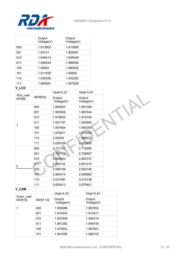
RDA5851 Datasheet V1.0
Output Voltage(V)
Output Voltage(V)
000 1.813802 1.810993001 1.83121 1.828281010 1.849414 1.846548011 1.869049 1.866056100 1.88952 1.886536101 1.911659 1.90852110 1.935356 1.932362111 1.960581 1.957629
V_LCD
Vlcd_vsel04H[9] 06H[8:6]
Vbat=4.2V Vbat=3.4V
Output Voltage(V)
Output Voltage(V)
1
000 1.884624 1.881268001 1.900926 1.897644010 1.918653 1.915154011 1.937167 1.933992100 1.957664 1.954354101 1.978871 1.975393110 2.00204 1.998532111 2.026158 2.022905
0
000 2.721137 2.716595001 2.763116 2.758507010 2.808443 2.803737011 2.856142 2.851215100 2.908199 2.903146101 2.962014 2.956682110 3.021087 3.015138111 3.083413 3.075401
V_CAM
Vcam_vsel04H[10] 06H[11:9]
Vbat=4.2V Vbat=3.4V
Output Voltage(V)
Output Voltage(V)
1 000 1.900696 1.897653001 1.916342 1.913417010 1.933346 1.930315011 1.951283 1.948154100 1.970642 1.967851101 1.991096 1.988103
RDA Microelectronics Inc. CONFIDENTIAL 76 / 88
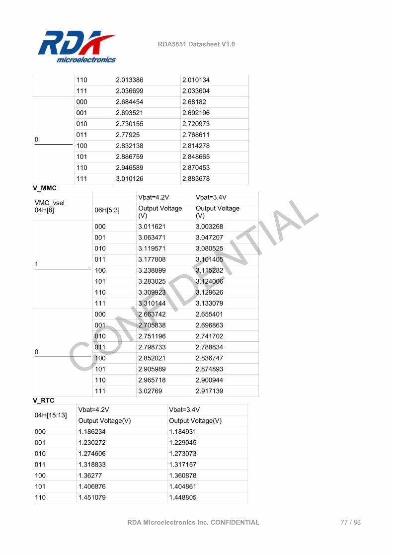
RDA5851 Datasheet V1.0
110 2.013386 2.010134111 2.036699 2.033604
0
000 2.684454 2.68182001 2.693521 2.692196010 2.730155 2.720973011 2.77925 2.768611100 2.832138 2.814278101 2.886759 2.848665110 2.946589 2.870453111 3.010126 2.883678
V_MMC
VMC_vsel04H[8] 06H[5:3]
Vbat=4.2V Vbat=3.4VOutput Voltage(V)
Output Voltage(V)
1
000 3.011621 3.003268001 3.063471 3.047207010 3.119571 3.080525011 3.177808 3.101405100 3.238899 3.115282101 3.283025 3.124006110 3.309923 3.129626111 3.310144 3.133079
0
000 2.663742 2.655401001 2.705838 2.696863010 2.751196 2.741702011 2.798733 2.788834100 2.852021 2.836747101 2.905989 2.874893110 2.965718 2.900944111 3.02769 2.917139
V_RTC
04H[15:13]Vbat=4.2V Vbat=3.4VOutput Voltage(V) Output Voltage(V)
000 1.186234 1.184931001 1.230272 1.229045010 1.274606 1.273073011 1.318833 1.317157100 1.36277 1.360878101 1.406876 1.404861110 1.451079 1.448805
RDA Microelectronics Inc. CONFIDENTIAL 77 / 88
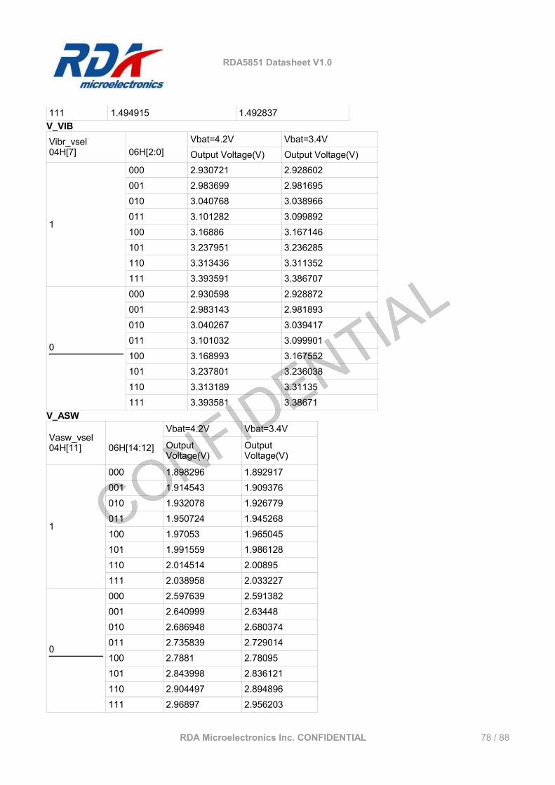
RDA5851 Datasheet V1.0
111 1.494915 1.492837V_VIBVibr_vsel04H[7] 06H[2:0]
Vbat=4.2V Vbat=3.4VOutput Voltage(V) Output Voltage(V)
1
000 2.930721 2.928602001 2.983699 2.981695010 3.040768 3.038966011 3.101282 3.099892100 3.16886 3.167146101 3.237951 3.236285110 3.313436 3.311352111 3.393591 3.386707
0
000 2.930598 2.928872001 2.983143 2.981893010 3.040267 3.039417011 3.101032 3.099901100 3.168993 3.167552101 3.237801 3.236038110 3.313189 3.31135111 3.393581 3.38671
V_ASW
Vasw_vsel04H[11] 06H[14:12]
Vbat=4.2V Vbat=3.4V
Output Voltage(V)
Output Voltage(V)
1
000 1.898296 1.892917001 1.914543 1.909376010 1.932078 1.926779011 1.950724 1.945268100 1.97053 1.965045101 1.991559 1.986128110 2.014514 2.00895111 2.038958 2.033227
0
000 2.597639 2.591382001 2.640999 2.63448010 2.686948 2.680374011 2.735839 2.729014100 2.7881 2.78095101 2.843998 2.836121110 2.904497 2.894896111 2.96897 2.956203
RDA Microelectronics Inc. CONFIDENTIAL 78 / 88
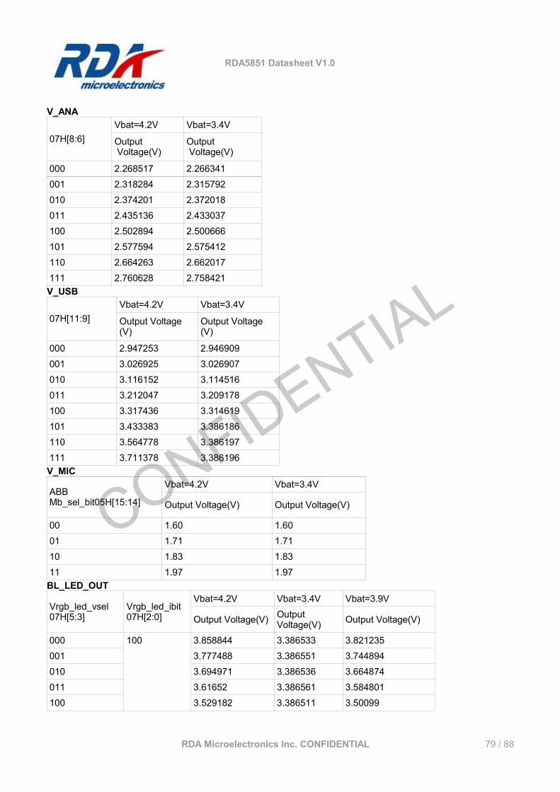
RDA5851 Datasheet V1.0
V_ANA
07H[8:6]Vbat=4.2V Vbat=3.4V
Output Voltage(V)
Output Voltage(V)
000 2.268517 2.266341001 2.318284 2.315792010 2.374201 2.372018011 2.435136 2.433037100 2.502894 2.500666101 2.577594 2.575412110 2.664263 2.662017111 2.760628 2.758421
V_USB
07H[11:9]Vbat=4.2V Vbat=3.4V
Output Voltage(V)
Output Voltage(V)
000 2.947253 2.946909001 3.026925 3.026907010 3.116152 3.114516011 3.212047 3.209178100 3.317436 3.314619101 3.433383 3.386186110 3.564778 3.386197111 3.711378 3.386196
V_MIC
ABB Mb_sel_bit05H[15:14]
Vbat=4.2V Vbat=3.4V
Output Voltage(V) Output Voltage(V)
00 1.60 1.60 01 1.71 1.71 10 1.83 1.83 11 1.97 1.97
BL_LED_OUT
Vrgb_led_vsel07H[5:3]
Vrgb_led_ibit07H[2:0]
Vbat=4.2V Vbat=3.4V Vbat=3.9V
Output Voltage(V) Output Voltage(V) Output Voltage(V)
000 100 3.858844 3.386533 3.821235001 3.777488 3.386551 3.744894010 3.694971 3.386536 3.664874011 3.61652 3.386561 3.584801100 3.529182 3.386511 3.50099
RDA Microelectronics Inc. CONFIDENTIAL 79 / 88
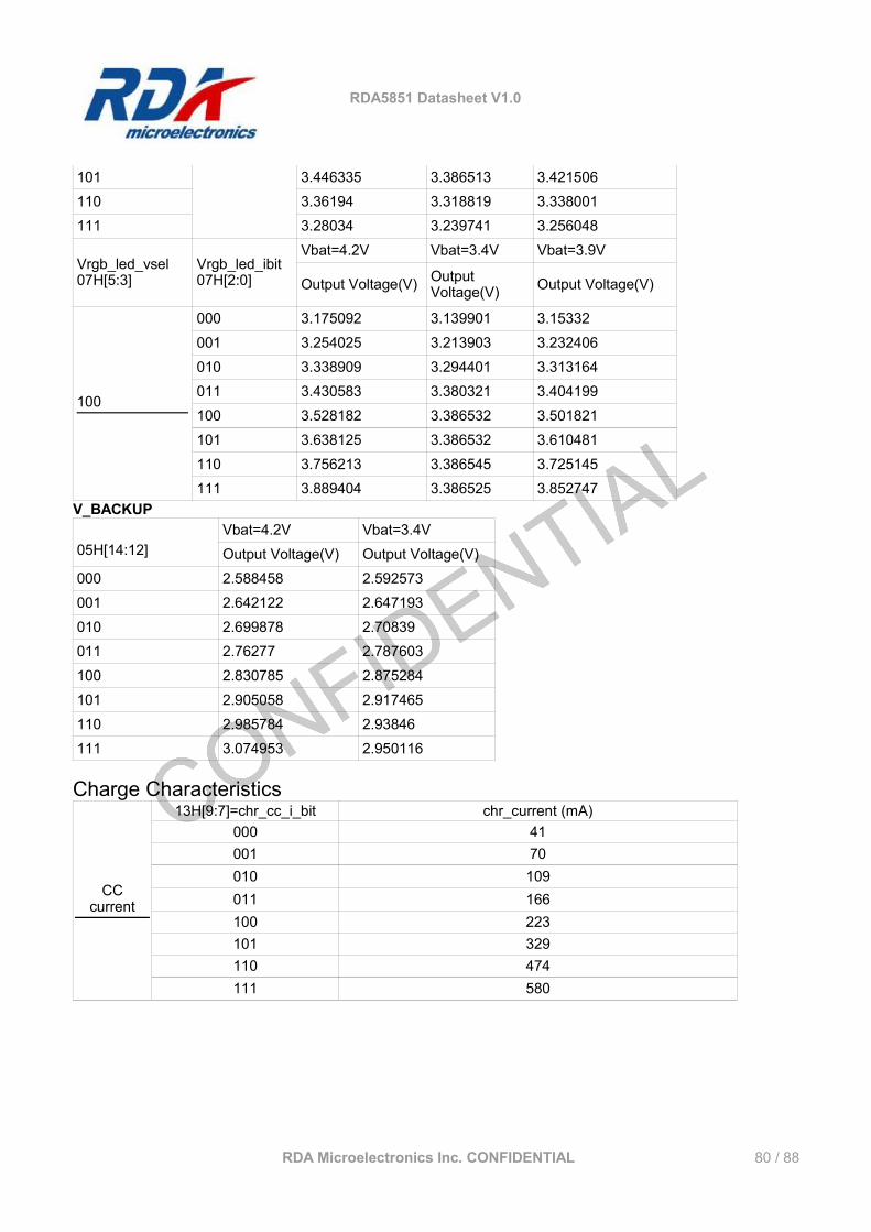
RDA5851 Datasheet V1.0
101 3.446335 3.386513 3.421506110 3.36194 3.318819 3.338001111 3.28034 3.239741 3.256048
Vrgb_led_vsel07H[5:3]
Vrgb_led_ibit07H[2:0]
Vbat=4.2V Vbat=3.4V Vbat=3.9V
Output Voltage(V) Output Voltage(V) Output Voltage(V)
100
000 3.175092 3.139901 3.15332001 3.254025 3.213903 3.232406010 3.338909 3.294401 3.313164011 3.430583 3.380321 3.404199100 3.528182 3.386532 3.501821101 3.638125 3.386532 3.610481110 3.756213 3.386545 3.725145111 3.889404 3.386525 3.852747
V_BACKUP
05H[14:12]Vbat=4.2V Vbat=3.4VOutput Voltage(V) Output Voltage(V)
000 2.588458 2.592573001 2.642122 2.647193010 2.699878 2.70839011 2.76277 2.787603100 2.830785 2.875284101 2.905058 2.917465110 2.985784 2.93846111 3.074953 2.950116
Charge Characteristics
CCcurrent
13H[9:7]=chr_cc_i_bit chr_current (mA)000 41001 70010 109011 166100 223101 329110 474111 580
RDA Microelectronics Inc. CONFIDENTIAL 80 / 88
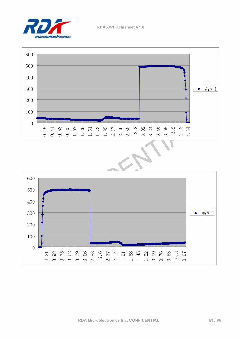
RDA5851 Datasheet V1.0
RDA Microelectronics Inc. CONFIDENTIAL 81 / 88
0
100
200
300
400
500
600
0.19
0.41
0.63
0.85
1.07
1.29
1.51
1.73
1.95
2.17
2.36
2.58
2.8
3.02
3.24
3.46
3.68
3.9
4.12
4.34
系列1
0
100
200
300
400
500
600
4.21
3.98
3.75
3.52
3.29
3.06
2.83 2.6
2.37
2.14
1.91
1.68
1.45
1.22
0.99
0.76
0.53 0.3
0.07
系列1
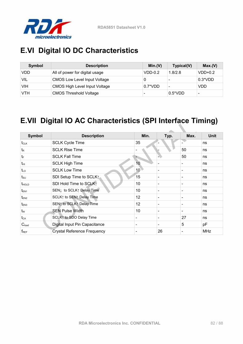
RDA5851 Datasheet V1.0
E.VI Digital IO DC Characteristics
Symbol Description Min.(V) Typical(V) Max.(V)VDD All of power for digital usage VDD-0.2 1.8/2.8 VDD+0.2
VIL CMOS Low Level Input Voltage 0 - 0.3*VDDVIH CMOS High Level Input Voltage 0.7*VDD - VDDVTH CMOS Threshold Voltage - 0.5*VDD -
E.VII Digital IO AC Characteristics (SPI Interface Timing)
Symbol Description Min. Typ. Max. UnittCLK SCLK Cycle Time 35 - - ns
tR SCLK Rise Time - - 50 nstF SCLK Fall Time - - 50 nstHI SCLK High Time 10 - - nstLO SCLK Low Time 10 - - nstSU SDI Setup Time to SCLK↑ 15 - - nstHOLD SDI Hold Time to SCLK↑ 10 - - nstEN1 SEN↓ to SCLK↑ Delay Time 10 - - nstEN2 SCLK↑ to SEN↑ Delay Time 12 - - nstEN3 SEN↑ to SCLK↑ Delay Time 12 - - nstW SEN Pulse Width 10 - - nstCA SCLK↑ to SDO Delay Time - - 27 nsCload Digital Input Pin Capacitance - - 5 pFfREF Crystal Reference Frequency - 26 - MHz
RDA Microelectronics Inc. CONFIDENTIAL 82 / 88
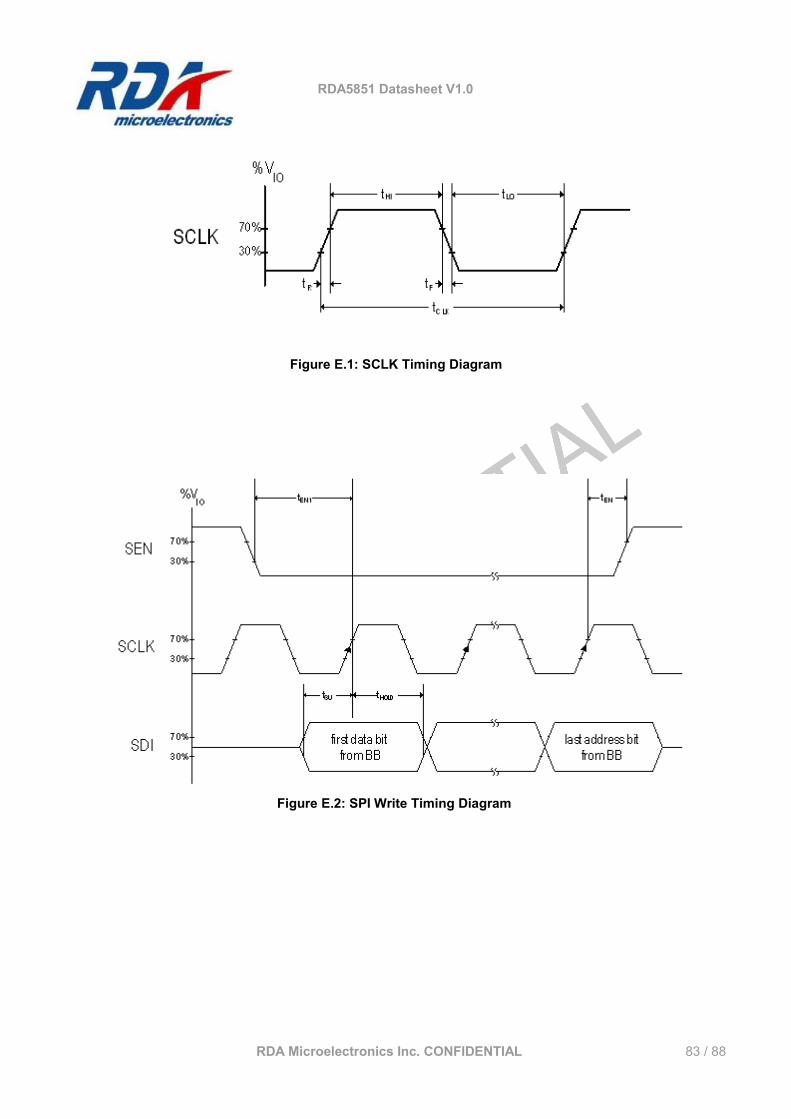
RDA5851 Datasheet V1.0
RDA Microelectronics Inc. CONFIDENTIAL 83 / 88
Figure E.2: SPI Write Timing Diagram
Figure E.1: SCLK Timing Diagram
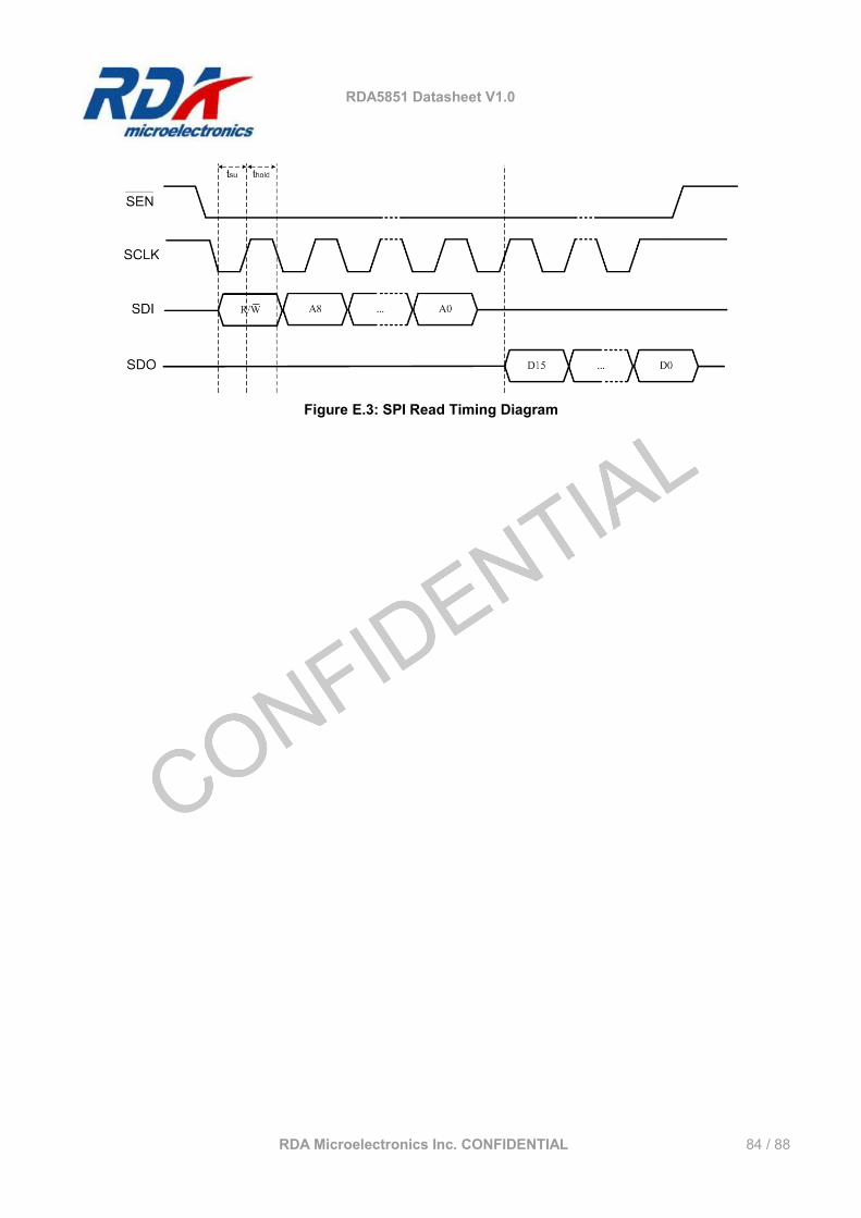
RDA5851 Datasheet V1.0
RDA Microelectronics Inc. CONFIDENTIAL 84 / 88
Figure E.3: SPI Read Timing Diagram
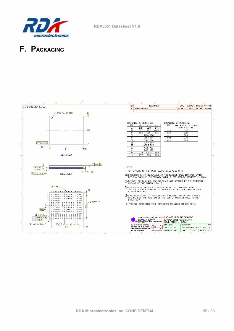
RDA5851 Datasheet V1.0
F. PACKAGING
RDA Microelectronics Inc. CONFIDENTIAL 85 / 88
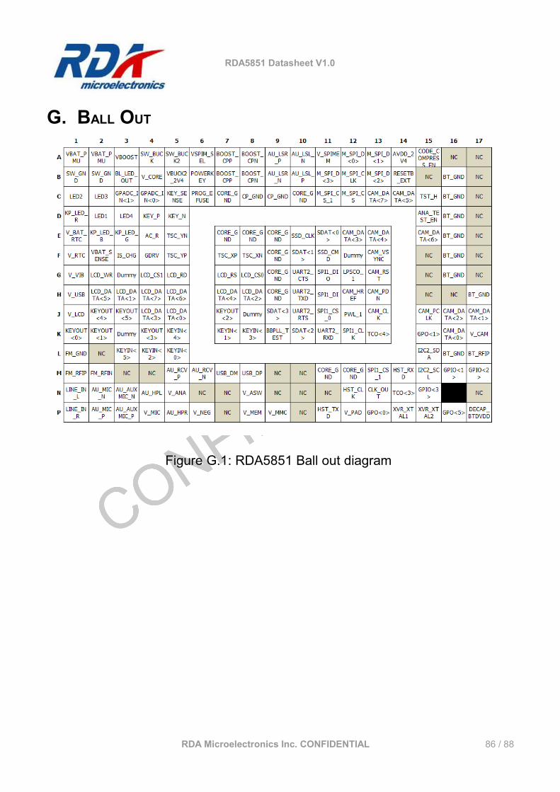
RDA5851 Datasheet V1.0
G. BALL OUT
Figure G.1: RDA5851 Ball out diagram
RDA Microelectronics Inc. CONFIDENTIAL 86 / 88
RDA5851 Datasheet V1.0
H. GLOSSARY
Name DescriptionAHB AMBA Advanced High-performance Bus.
AHB2AHB Bridge allowing Sys AHB to communicate with BB AHB, and vice versa.AIF RDA5851's Audio Interface, including PCM, DAI and Audio Analog Interface.APB AMBA Advanced Peripheral Bus, slow bandwidth bus.ATR Answer To Reset, see SCI module for details.
Comfort Tone Tone generated by the AIF, used to indicate ringing, occupied...CS Chip Select.DAI Digital Audio Interface, part of the AIF used for test purpose.
DMA Direct Memory Access, can copy a part of the memory at an other address.DTMF Dual Tone Multi Frequency generated by the AIF when a number is dialed.EBC External Bus Controller, to connect external RAM, polyphonic chips, MMC...ETU Elementary Time Unit, see SCI module for details.
GP ADC General Purpose Analog to Digital Converter.IFC Base Band Intelligent Flow Controller, a bridge between AHB and APB buses.IrDA Infra Red communication protocol used by RDA5851's UART infra red mode.
Mailbox Communication module between the Sys AHB bus and the BB AHB bus.MMC Multi Media Chips.MMI Man-Machine Interface, a part of the software that handle the user interface.PCM Pulse Code Modulation, the part of the AIF that outputs samples in serial.PLL Phase-Locked Loop.SPI Serial Peripheral Interface.Sys System side of RDA5851, dedicated to the application, MMI.TCO Time-Controlled Output. Pins controlled by the TCU.TCU Timing Control Unit, handle the scheduling of individual events.
UART Universal Asynchronous Receiver Transmitter, asynchronous serial port.VCO Voltage Controlled Oscillator.
XCPU System RDA's 16/32-bit RISC CPU.
RDA Microelectronics Inc. CONFIDENTIAL 87 / 88
RDA5851 Datasheet V1.0
Document HistoryThe evolution of this document is described in the following table:
Version Date Description1.00 2013-01-29 Initial version.
RDA Microelectronics Inc. CONFIDENTIAL 88 / 88