rapid prototyping tools for power electronic converters
TRANSCRIPT

University of ConnecticutOpenCommons@UConn
Master's Theses University of Connecticut Graduate School
5-6-2014
Rapid Prototyping Tools for Power ElectronicConvertersAmruta V. KulkarniUniversity of Connecticut - Storrs, [email protected]
This work is brought to you for free and open access by the University of Connecticut Graduate School at OpenCommons@UConn. It has beenaccepted for inclusion in Master's Theses by an authorized administrator of OpenCommons@UConn. For more information, please [email protected].
Recommended CitationKulkarni, Amruta V., "Rapid Prototyping Tools for Power Electronic Converters" (2014). Master's Theses. 576.https://opencommons.uconn.edu/gs_theses/576

i
Rapid Prototyping Tools for Power Electronic Converters
Ms. Amruta Vasant Kulkarni
B.E., University of Pune 2008
A Thesis
Submitted in Partial Fulfillment of the
Requirements for the Degree of
Master of Science
At the
University of Connecticut
2014

ii
APPROVAL PAGE
Master of Science Thesis
Rapid Prototyping Tools for Power Electronic Converters
Presented by
Amruta V. Kulkarni, B.E.
Major Advisor____________________________________________________________
Dr. Ali Bazzi - University of Connecticut
Associate Advisor_________________________________________________________
Dr. Krishna R. Pattipati - University of Connecticut
Associate Advisor_________________________________________________________
Dr. Sung Yeul Park - University of Connecticut
University of Connecticut
2014

iii
ACKNOWLEDGEMENTS
I take this opportunity to express my profound gratitude and deep regards to my advisor
Prof. Ali Bazzi for his exemplary guidance, mentoring and constant encouragement throughout
the course of this thesis. The help and guidance given by him from time to time was instrumental
in making my research a success. I would also like to express a deep sense of gratitude to Dr.
Krishna Pattipati and Dr. Sung Yeul Park for their cordial support, valuable information and
guidance, which has helped me in completing this task well through various stages. I am obliged
to my colleagues in the Advanced Power Electronics and Electric Drives Lab (APEDL) lab for
the constant and extremely valuable help provided by them. I am grateful for their cooperation
during the period of my research through numerous problem solving and idea-sharing exercises.
I thank my parents Mrs. Madhuri Kulkarni and Mr. Vasant Kulkarni for preparing me to succeed
in all walks of life and my husband Mr. Hrushikesh Gandhi for standing by me through this
entire endeavor. Lastly, all my friends and family members deserve a big thanks for their
constant encouragement without which this day would not be possible.

iv
TABLE OF CONTENTS
List of Tables.................................................................................................................................vii
List of Figures..................................................................................................................................x
Abstract……………………………………………………………………………………....….xiii
CHAPTER 1 INTRODUCTION...............................................................................................................1
CHAPTER 2 LITERATURE REVIEW ....................................................................................................5
2.1 Power Loss Modeling...................................................................................................5
2.1.1 Power Loss Models for Components………………………………………..5
2.1.2 Power Loss Models for Power Electronic Converters………………..…..…9
2.1.3 Power Losses Calculation Methods………………………………………..10
2.2 Cost Modeling……………………………………………………………………....11
2.2.1 Cost Models for Components……………………………………………...11
2.2.2 System Cost Models…...…………………………………………….….....14
2.3 Reliability Modeling………………………………………………………………..16
2.3.1 Reliability Models for Power Electronic Components and Converters..…..17
2.3.2 Reliability Modeling and Rapid Prototyping Methods.…………………....20
2.4 Summary of Literature Review Findings...…………………………………….…...22
CHAPTER 3 POWER LOSS MODELS FOR CONVERTERS…................................................................24
3.1 Generalized Component-Level Power Loss Models………………………………..25
3.1.1 MOSFET Losses………………………………………………………...…26
3.1.2 Diode Losses…………………………………………………………….…27
3.1.3 Inductor Losses……………………………………………………….……28
3.1.4 Capacitor Losses………………………………………………………...…30
3.1.5 PCB Losses……………………………………………………………...…30
3.1.6 Gate Drive Losses…………………………………………………….……31
3.2 Power Loss Models for Several Converters…………………………………….…...32
3.2.1 Boost Converter in CCM…………………………………………..………33
3.2.1.1 MOSFETs Losses……………………………………………………..33
3.2.1.2 Diode Losses………………………………………….……………….34
3.2.1.3 Inductor Losses………………………………………………………..34
3.2.1.4 Capacitor Losses………………………………………………………35

v
3.2.2 Buck Converter in CCM………………………...…………………………35
3.2.2.1 MOSFETs Losses……………………………..………………………35
3.2.2.2 Diode Losses…………………………………….…………………….36
3.2.2.3 Inductor Losses…………………………………..……………………36
3.2.2.4 Capacitor Losses………………………………………………………36
3.2.3 Flyback Converter in DCM……………………………………..……...…36
3.2.3.1 MOSFET Losses……………………………………………...……….37
3.2.3.2 Diode Losses……………………………………………….………….38
3.2.3.3 Flyback Coupled-Inductor/Transformer Lossses……………...………38
3.2.3.4 Capacitor Losses……………………………………………...……….39
3.2.3.5 Snubber Circuit Power Losses………………………………...………39
3.3 Results ………………………………………………………………...……………40
3.3.1 Boost Converter Results……………………………………...……………42
3.3.2 Buck Converter Results……………………………………...…………….45
3.3.3 Flyback Converter Results………………………..………………………..48
CHAPTER 4 COST MODEL FOR CONVERTERS..................................................................................51
4.1 MOSFET Cost Model………………………………...……………………..…...…52
4.2 Diode Cost Model …………………………………..………………………..….…54
4.3 Inductor Cost Model……………………….………….……………………………57
4.4 Capacitor Cost Model……….…………………...…………………………………59
4.5 Cost Model for Flyback Coupled-Inductor/ Transformer Cores………………...…61
4.6 Magnet Wire Cost Model……………………………..………….…………………63
4.7 Cost Model Results………….…………………………………………………...…65
CHAPTER 5 RAPID PROTOTYPING TOOLS FOR POWER LOSS AND COST MODELS …………………67
5.1 Rapid Prototyping Tools: Component-specific Mode…………………...................69
5.1.1 Power Loss Modeling in the Component-specific Mode……………….…69
5.1.1.1 Pseudo Code for Power Loss Modeling in the Component-specific
Mode…………………………………………………………………………..70
5.1.1.2 Flowchart for Power Loss Modeling in the Component-specific Mode71
5.1.1.3 Results for Power Loss Modeling in the Component-specific Mode…72
5.1.2 Cost Modeling in the Component-specific Mode………………………….73
5.1.2.1 Pseudo Code for Cost Modeling in the Component-specific Mode…..74
5.1.2.2 Flowchart for Cost Modeling in the Component-specific Mode……...74

vi
5.1.2.3 Results for Cost Modeling in the Component-specific Mode……...…75
5.2 Rapid Prototyping Tools: Optimization Mode………………..………………..……76
5.2.1 Power Loss Modeling in the Optimization Mode ………………………77
5.2.1.1 Component Selection Procedure ……………………………………...77
5.2.1.2 Pseudo Code for Power Loss Modeling in the Optimization Mode…..81
5.2.1.3 Flowchart for Power Loss Modeling in the Optimization Mode...……81
5.2.1.4 Results for Power Loss Modeling in the Optimization Mode………...83
5.2.2 Cost Modeling in the Optimization Mode………………..……………..…86
5.2.2.1 Pseudo Code for Cost Modeling in the Optimization Mode..................87
5.2.2.2 Flowchart for Cost Modeling in the Optimization Mode…………......87
5.2.2.3 Results for Cost Modeling in the Optimization Mode …….………….89
CHAPTER 6 CONCLUSION AND FUTURE WORK …………………………………………...………96
APPENDIX ………………………………………………………………………………..……… 99
APPENDIX I COMPONENT-SPECIFIC MODE RESULTS FOR DIFFERENT DUTY RATIOS……...99
APPENDIX II OPTIMIZATION MODE RESULTS FOR DIFFERENT DUTY RATIOS…...………102
APPENDIX III DETAILED DERIVATION OF EQUATIONS…………………………………..108
Appendix IV COST MODEL EQUATIONS WITH DIFFERENT SURFACE FITS………………111
REFERENCES…………………………………………………………………………………….113

vii
LIST OF TABLES
Table I: Example testing conditions and parasitic elements in experimental prototypes…..........41
Table II: Estimated and measured power loss in boost converter…………………………..…...42
Table III: Detailed boost converter component power losses for different duty ratios…….……43
Table IV: Estimated and measured power loss in buck converter………………………….……45
Table V: Detailed buck converter component power losses for different duty ratios………...…46
Table VI: Estimated & measured power loss in flyback converter………………………..…….48
Table VII: Detailed flyback converter component power losses for different duty ratios……....48
Table VIII: αi Coefficients and ranges………………………………………...…………………53
Table IX: δj coefficients for diode cost model equations……………...…….…………...……...55
Table X: Inductor cost model coefficients……………………………………………………….57
Table XI: ηz coefficients and ranges……….…………………...……………………………….59
Table XII: τm Coefficients and ranges………………………...………………………………….61
Table XIII: Wire gauge and its current capacity…………………………………………………63
Table XIV: φq coefficients and ranges……………………………………...……………………64
Table XV: Detailed cost comparison for power components……………….…………………...65
Table XVI: Boost converter results generated by power loss modeling tool...………………….85
Table XVII: Buck converter results generated by power loss modeling tool……………………85
Table XVIII: Flyback converter results generated by power loss modeling tool……………...86
Table XIX: Boost converter results generated by optimization mode cost modeling tool with
minimum cost as the optimization objective…..………………………………………………...90
Table XX: Boost converter results generated by optimization mode cost modeling tool with
lowest power loss as the optimization objective…………………………………………………91

viii
Table XXI: Buck converter results generated by optimization mode cost modeling tool………92
Table XXII: Flyback converter results generated by optimization mode cost modeling tool…...94
Table A1: Boost converter component-specific mode results for different duty ratios…..…..….99
Table A2: Buck converter component-specific mode results for different duty ratios…..…..…100
Table A3: Flyback converter component-specific mode results for different duty ratios……...101
Table A4: Boost and buck converter parameters for GUI model………………………..……102
Table A5: Boost converter power loss model results for Case 1………………………….……102
Table A6: Boost converter power loss model results for Case 2………………………….……102
Table A7: Boost converter power loss model results for Case 3……………………………….103
Table A8: Buck converter power loss model results for Case 1………………………………..103
Table A9: Buck converter power loss model results for Case2………………………………...104
Table A10: Buck converter power loss model results for Case3……………………………….104
Table A11: Boost converter cost model results for Case 1……………………………………..105
Table A12: Boost converter cost model results for Case 2……………………………………..105
Table A13: Boost converter cost model results for Case 3……………………………………..106
Table A14: Buck converter cost model results for Case 1……………………………………...106
Table A15: Buck converter cost model results for Case 2……………………………………...107
Table A16: Buck converter cost model results for Case 3………………………………...……107
Table A17: Surface fitting tool equations for MOSFET ………………………………....……111
Table A18: Surface fitting tool equations for diode ………………………………..…...……111
Table A19: Surface fitting tool equations for inductor ………………………………….……111
Table A20: Surface fitting tool equations for capacitor…………………………………...……112

ix
Table A21: Surface fitting tool equations for cores…………………..…………………...……112
Table A22: Curve fitting tool equations for magnet wire…….…………………………...……112

x
LIST OF FIGURES
Figure 1: Bath tub curve ……………………………………………………….…......................16
Figure 2: Example illustration on how to aggregate component level models into a system……24
Figure 3: MOSFET model with non-idealities…………………………………..………………26
Figure 4: MOSFET drain current……………………………………………….…......................26
Figure 5: Diode model with non-idealities………………………………………........................27
Figure 6: Inductor model with non-idealities……………………………………….....................29
Figure 7: Inductor current waveform……………………………………….................................29
Figure 8: Capacitor model with non-idealities………………………………………...................30
Figure 9: PCB equivalent model………………………………..………………………………..30
Figure 10: Gate drive ICs equivalent model…………………..…………………........................32
Figure 11: Boost converter with its non-idealities………………………………….....................33
Figure 12: Buck converter topology for power loss model…………………..............................35
Figure 13: Flyback converter model with its non-idealities…………………..............................37
Figure 14: MOSFET switching waveform………………………....……………........................37
Figure 15: Inductor switching waveform………………………………………...........................38
Figure16: Experimental setup for the buck and boost converters……………..............................41
Figure 17: Boost converter results for 30% duty……………………...........................................43
Figure 18: Boost converter results for 40% duty ratio………………………….…......................44
Figure 19: Boost converter results for 50% duty ratio…………………………….......................44
Figure 20: Boost converter results for 60% duty ratio…………………………….......................44
Figure 21: Boost converter results for 75% duty ratio…………………………….......................45
Figure 22: Buck converter results for 20% duty ratio ………………………………...................46
Figure 23: Buck converter results for 30% duty ratio………………………………....................47

xi
Figure 24: Buck converter results for 40% duty ratio………………………………....................47
Figure 25: Buck converter results for 50% duty ratio…………………………………...............47
Figure 26: Flyback converter results for 20% duty ratio …………………………....................49
Figure 27: Flyback converter results for 30% duty ratio……………………………...................49
Figure 28: Flyback converter results for 40% duty ratio……………………………...................49
Figure 29: Flyback converter results for 50% duty ratio……………………………...................50
Figure 30: MOSFET cost model for one unit………………………………………....................54
Figure 31: MOSFET cost model for 1000 units……………………………………....................54
Figure 32: Diode cost model for one unit………………………………………..........................56
Figure 33: Diode cost model for 1000 units………………………………………......................56
Figure 34: Inductor cost model for one unit………………………………………......................58
Figure 35: Inductor cost model for 1000 units………………………………………...................58
Figure 36: Capacitor cost model for one unit………………………………………....................60
Figure 37: Capacitor cost model for 1000 units……………………………………….................60
Figure 38: Core cost model for one unit………………………………………............................62
Figure 39: Core cost model for 1000 units………………………………………………………62
Figure 40: Magnet wire cost model for single bundle………………………...............................64
Figure 41: Procedure for the proposed rapid prototyping tool………..……………....................68
Figure 42: Overall procedure for power loss modeling in Component-specific mode……..........71
Figure 43: GUI showing component-specific mode boost converter power loss model...............72
Figure 44: GUI showing component-specific mode buck converter power loss model................73
Figure 45: GUI showing component-specific mode flyback converter power loss model............73
Figure 46: Flowchart for cost model in component-specific mode…….......................................75
Figure 47: GUI for component cost estimates in component-specific mode…….........................76

xii
Figure 48: Optimization tool for minimum power loss & component selection...........................82
Figure 49: Optimization mode boost converter power loss modeling & component selection.....83
Figure 50: Optimization mode buck converter power loss modeling & component selection......84
Figure 51: Optimization mode flyback converter power loss modeling & component selection.84
Figure 52: Optimization mode flowchart for cost modeling tool……..........................................88
Figure 53: Boost converter optimization mode cost modeling tool…………...............................89
Figure 54: Buck converter optimization mode cost modeling tool…………..…………………..92
Figure 55: Flyback converter optimization mode cost modeling tool………….………………..93

xiii
ABSTRACT
In recent years, demand for utilization of power electronic converters in industrial,
commercial and household applications has increased significantly. It is critical for engineers to
design these converters in a short duration. Considering the time constraints on engineers it’s not
surprising that rapid prototyping tools have become very popular in the industry. Through rapid
prototyping, users can estimate power loss and cost which are essential to design decisions. The
research presented here treats main power electronic components of a converter as building
blocks that can be arranged to obtain various topologies to facilitate rapid prototyping. In order
to get system-level power loss and cost models, two processes are implemented. The first process
automatically provides minimum power loss or cost estimates and identifies components for
specific applications and ratings; the second process estimates power losses and costs of each
component of interest as well as the whole system. Power loss models are analytical and include
effects of parasitic elements and non-idealities. Cost models for each building block are derived
based on an extensive market survey. Three examples are used to illustrate the proposed research
- boost and buck converters in continuous conduction mode (CCM) and flyback converter in
discontinuous conduction mode (DCM). Optimization of component selection is based on the
minimum possible cumulative power loss in these components or minimum cumulative cost of
components. These techniques help engineers to select the best components for their applications
and aid researchers in prototyping different converters for several applications. The proposed
cost and loss estimates are shown to be over 92% accurate when compared to measured losses
and real cost data. This research presents derivations of the proposed models, detailed
experimental measurements and demonstration of a friendly user interface that integrates all the
models.

1
CHAPTER 1: INTRODUCTION
Power electronics literature and patent records over many years show radical developments
and modifications in power electronic converters. In the early 1960’s, basic converters such as
boost, buck and flyback converters were developed by utilizing semiconductor devices [1]. As
progress in the performance, efficiency and structure of semiconductors increased, basic
converters were modified for different applications and requirements. For instance, DC-DC
converters were developed for automobile applications [1, 2], high frequency DC-DC switching
converters [3, 4] or switched mode power supplies [5, 6] began to be used in battery chargers,
home appliances, hybrid electric vehicles, and many other applications. Also, resonant switching
converters [7, 8] were observed as an efficient solution for lighting applications, smart grids,
renewable energy systems and power supplies [9]. Thus, today power electronic converters are in
high demand in many areas of electrical and electronics technology.
The diversity of applications, power ratings, and energy levels of power electronic converters
require different converter topologies and ratings with numerous component options and
combinations. The design of high efficiency, cost effective and reliable power converters in a
short time is a challenging task for any power electronics engineer. A designer has to review a
vast amount of existing literature, datasheets and web-based information in order to select a
single component. Thus, researchers find it beneficial to work on developing tools which can
help select appropriate components for new converter designs so that they can achieve minimum
power loss and/or minimum cost for their application.
Over the past few decades, several power loss and cost estimation models or methods have
been developed for power converters. When designers first start to design a converter, they have
to start with the ratings and from an application point of view. Thus, it has become a critical

2
issue to develop rapid prototyping tools or methods on the basis of the specifications. The power
loss models developed in the existing literature do not always consider most non-idealities and
parasitic elements. Furthermore, printed circuit board (PCB) and gate drive losses are not
observed along with component power losses in some existing power loss rapid prototyping
tools. From a cost perspective, even though cost is a major driving factor for the power
electronics industry, research literature shows limited cost models. Moreover, user-friendly rapid
prototyping tools, which can accurately estimate the cost and power loss of a component as well
as the whole system in a short time, are not present in the literature. The techniques and
methodologies which are observed in the literature are described in detail in Chapter 2.
Rapid prototyping tools based on power loss and cost models are expected to reduce
engineering time and enhance product cost and quality in electronic manufacturing in many
applications such as DC-DC converters, inverters, LED drivers, smart grid systems.
Rapid prototyping tools for DC-DC converters are of main interest here due to the
converters’ simplicity, wide range of their applications and since the methodology for
developing models is of main interest here. The main goal of this research is thus to achieve
rapid prototyping capability through a systematic methodology to estimate and minimize power
losses and cost of DC-DC converters. Generalized power loss equations for fundamental power
electronic components are composed from existing literature and then reformulated in terms of
input and output requirements, switching frequencies and duty ratio to obtain a simple and
uniform approach in power loss estimation tools for different converters. To validate these tools,
boost and buck converters in continuous conduction mode (CCM) and flyback converter in
discontinuous conduction mode (DCM) are implemented since they are widely applicable and
popular among power electronic converters. It is important to note that methodology developed

3
in this research can be extended for other converters, inverters as well as other electronic
development applications. On the other hand, cost models are based on an extensive market
survey of component costs. A database for all applicable components is used to model costs of
these components using their major ratings and values, e.g. cost of a capacitor is modeled as
dependent on capacitance and voltage rating. The power loss and cost models are then integrated
into the rapid prototyping tools developed using a MATLAB Graphical User Interface (GUI).
The power loss and cost model presented here are only for power electronic components.
However, connectors’ power loss and cost models are not included. The rapid prototyping tools
based on these models can use component-specific information, or can run in optimization mode
which can perform converter component selection for power loss minimization or cost
minimization. A major goal for these tools is to minimize the estimation error when comparing
actual component cost and power loss values with the measured or real ones, and their main
advantage is the ability to evaluate a large number of possible component combinations and
achieve instantaneous cost and loss estimates. It is important to note that the models provided
here can easily evolve over time and changes in technology and cost.
In addition to power loss and cost models, researchers and designers are very interested in the
reliability estimation and prediction techniques. Several methods and models have been proposed
to estimate the reliability of components and derive accelerated testing methods for power
electronic systems. These methodologies are discussed in detail in Chapter 2, but as reliability is
a broader topic for research, rapid prototyping methods proposed here are limited to the power
loss and cost estimation techniques while rapid prototyping tools based on reliability and
accelerated testing methods can be developed in the future research.

4
The thesis proceeds as follows. Chapter 2 discusses existing literature for power loss, cost
and reliability models. This includes power loss estimation and reduction techniques for system
level and component level power losses, cost, as well as reliability. It provides deep insight into
the topic and helps to develop rapid prototyping tools and concludes with the discussion of
limitations of existing literature. Chapter 3 describes the concept behind power loss models,
procedures for rapid prototyping tools for power loss models in optimization mode and
component-specific mode, derivations of power loss model equations for basic building block
components, and reformulation of these equations for boost, buck and flyback converters.
Chapter 4 presents cost estimation methodology in optimization mode and component-specific
mode with cost surfaces based on a large database of basic building block components. Chapter 5
elaborates on the optimal selection of components using the rapid prototyping tools, in addition
to component-specific cost and power loss models. Research conclusions are covered in Chapter
6, which also provides recommendations for future research efforts. The Appendix includes
detailed results for case studies of component-specific and optimization modes for various
converters and different operating points, along with experimental verification of the provided
models and detailed derivation of mathematical expressions.
Related Publications
[1] A.V. Kulkarni, A. M. Bazzi, " Empirical Cost and Analytical Power Loss Models of DC-DC
Inductors," in Proceedings of Electrical Manufacturing & Coil Winding Association, Milwaukee,
Wisconsin, May 2013.
[2] A.V. Kulkarni, A. M. Bazzi, “A Building-Block Approach to Efficiency and Cost Models of
Power Electronic Systems," in Proceedings of the IEEE Applied Power Electronics Conference
and Exposition , Dallas Forth worth, Texas, March 2014.

5
CHAPTER 2: LITERATURE REVIEW
Contributions from existing literature help to develop the concepts upon which the power
loss and cost models are built and to highlight the ways in which power loss and cost models
developed here are different. An important take-away from this chapter is that while the vast
literature reviewed here does not address non-idealities and parasitic elements frequently, the
power loss model presented here does focus on these elements along with PCB and gate drive
losses leading to more accurate power loss models. The cost models developed in this research
are based on an extensive market survey. The most important aspect of this research is that the
power loss and cost modeling methodologies developed here are such that they can evolve over
time and changes in technology. Subsequent sections of this chapter address related work on
power loss, cost, and reliability models, and rapid prototyping methods.
2.1 Power Loss Modeling
This section provides information about the existing power loss models for components and
converters. This information helps uncover the problems associated with existing power loss
estimation models and aids to develop more accurate models. This section also describes power
loss estimation methods and their advantages and disadvantages. Section 2.1.1 reviews power
loss models of power electronic components. Section 2.1.2 reviews system-level power loss
estimation models, and Section 2.1.3 summarizes different power loss estimation methods.
2.1.1 Power Loss Models for Components
Several techniques have been implemented to find the power losses in power electronic
component. Majority of the research has focused on selecting components for power electronic
converters, e.g. [10]. Extensive research has been conducted for finding specific losses in

6
semiconductors and magnetic components. For example, in [11] a qualitative analysis is carried
out on six non-isolated DC-DC topologies such as buck, boost, buck-boost, Ćuk, SEPIC, and
Zeta to select components for these converters. This process is then verified with the help of
conduction and switching losses in the MOSEFTs and IGBTs, but gate losses in IGBTs and
MOSFETs are ignored in this research.
The conduction and switching losses estimation in MOSFETs and IGBTs in boost converter
CCM are given in [11] as,
2C CS CDP P P
D . (1)
where PC is the MOSFET loss, PCS is the MOSFET switching loss, PCD is the MOSFET
conduction loss and D is the duty ratio. A similar approach has been developed in [12] for the
DC converters which are used in telecommunication applications. The conduction power loss in
MOSFET and its Schottky barrier diode conduction losses are observed but switching losses
within it are ignored. In order to estimate exact power loss of MOSFET or IGBTs the
conduction, switching and gate drive losses must be considered.
The conduction and switching losses should both be considered while calculating the diode
total power loss. In [13] conduction losses of flyback diodes are obtained using three simple
tasks viz. estimation of maximum power loss consumption, nonlinear finite element analysis of
diode losses and actual implementation of these analyses in the flyback converter experiment.
This approach gives a deeper insight into diode conduction power loss estimation, but it fails to
explain how to measure switching losses in the flyback converter diode. In [14], while
calculating light load efficiency of a buck converter with diode emulation method, switching
losses of MOSFET and its effect on the diode power loss were considered but effect of diode
switching loss on the total system-level loss was ignored. The MOSFET switching loss in the

7
buck converter is given as,
_ ( ) ( ) _
1( )
2Switch ctrl CCM in o CCM f ctrl swP V I i t f . (2)
where PSwitch_ctrl(CCM) is the switching losses of buck converter in CCM, fsw is the switching
frequency, Vin is the input voltage, tf_ctrl is the MOSFET fall times, Io is the output current and
∆i(CCM) is the inductor current ripples in CCM. An inductor core loss estimation method has been
proposed in [15] for PFC application. This method is based on the Steinmetz equation, but for
high switching power converters this equation is modified as,
1 / (2 ) / / (2 ) /m n m nCORE e on on S on off SP K V B T T T B T T T
(3)
where ∆Bm is the maximum peak flux density, Ton is the interval when MOSFET is ON, Toff is
the interval when MOSFET is OFF, TS is the MOSFET switching time, Ve is the effective core
volume, K1 is the inductor core material constant and n is transformation ratio. The above
equation considers the effect of high switching frequency on the core loss and the B-H curve.
However, [15] did not consider the winding copper loss and the skin effect on core losses which
is usually observed at high frequencies. For higher switching frequencies, lower power loss is
observed in the copper windings in [16]. In this research the copper windings are used with
center-gapped, side-gapped and spacer configuration cores. Copper loss estimation tools are
developed for the inductors with these cores, but a generalized copper loss model is not
considered.
Power losses in capacitors are generally lower as compared to power losses in other
components. The power loss within a capacitor is calculated by combination of the power losses
in ESR and the parallel parasitic resistance across it. For instance, fault detection and power loss
estimation formulae are given in [17] for various switching frequencies in a PFC circuit. The

8
total power loss in the capacitor is shown as,
2( ) ( )
1
N
LOSS k k
k
P ESR I
(4)
where PLOSS is the power loss in capacitor, ESR is the equivalent series resistance, I is the
capacitor current and k is the of harmonic order of the capacitor current. Similar to the power
electronic components, the power loss estimation tools for PCBs and gate drive circuits are also
observed in the literature. The procedures for proximity loss and conduction loss in PCBs are
discussed in [18] with the help of finite element analysis. The proximity losses are obtained in
[18] as,
2. ., ,
2( , , )proxu l x prox x oxP w h de H
. (5)
In this equation Pproxul,x is the proximity losses of the PCB, prox,x is the geometry dependences of
the conduction losses in traces, w is the width of the trace, h is the height of the trace, Hax is the
external magnetic field generated, de is the skin depth and σ is the conductivity of conductor. To
analyze the high frequency power loss in a PCB, the analogy of basic principles of
electromagnetic wave propagation in periodic media has been used in [19].
Methods for estimation and reduction of gate drive circuit power losses are proposed in [20]
with the help of switching frequency and MOSFET gate to source capacitance. However, power
losses within the gate drive capacitances are ignored in it. In [21], analytical power loss model is
developed for the MOSFET and its current source resonant gate driver but power losses within
bootstrap capacitor circuit are ignored. The total power loss in the gate driver IC is,
2GDRV DD g swP V C f (6)
where VDD is the gate drive IC supply pin and Cg is the gate capacitance.

9
2.1.2 Power Loss Models for Power Electronic Converters
Detailed analysis of power losses in different converters is further described in this subsection
along with topology-specific power loss models. For example, power losses within a boost
converter caused by reverse recovery characteristics of the rectifier have been modeled for
minimization in [22]. Some researchers have also worked on specific component losses in the
converters such as MOSFET losses in a boost converter [23]. Total system-level power losses
are also discussed in the literature, for example the total boost converter power loss and its
component losses in [24]. The total boost converter power losses are given in [24] as,
loss cond fixed TOT swP P P W f , (7)
where the boost converter power losses depend on the conduction losses in the MOSFET
and diode (Pcond), fixed losses of other components (Pfixed), and dynamic losses (WTOT) that vary
with the switching frequency (fsw).
Most of the research in converter power loss modeling is targeted towards power loss
estimation and component selection procedure for the converters. For instance, a dynamic power
loss (PD) model based on transient loss (PT), datasheet parameters (Pf) and parasitic elements of
the components (Pr) is developed for the buck converter in [25]. It also provides component
selection procedure for the buck converters, but PCB and gate drive circuit losses are ignored.
Dynamic losses of each component in the converter are approximated as,
D f r TP P P P (8)
Also, a power loss calculation method for power MOSFETs in buck converters is given in [26].
Power loss reduction techniques are also provided in the literature. For example, power loss
reduction techniques for active clamped flyback converter are shown in [27]. However, this
method fails to explain power loss estimation techniques in flyback or active clamped flyback

10
circuits. Another example is [28], where with the help of the Dowell equation, a power loss
model for flyback transformer windings considers skin and proximity losses. The primary and
secondary winding power loss of flyback transformer at various harmonics is given as,
wp wpdc RpnP P F (9)
ws wsdc RsnP P F . (10)
FRpn and FRsn are derived from Fourier transforms which provide the power loss values at various
harmonics, Pwp is the primary winding power loss, Pwpdc is the primary winding DC power
loss, Pws is the secondary winding power loss and Pwsdc is the secondary winding DC power loss.
Some research also offers power loss estimation methods for flyback converters in DCM but
ignores snubber circuit power loss estimation as in [29] where power loss in primary and
secondary switches, magnetic components, and gate drive circuits are presented but snubber
circuit power losses are ignored.
2.1.3 Power Losses Calculation Methods
Several methods to measure system-level power losses have been presented in the literature.
For example, references [30] and [31] provide electrical and calorimetric methods. Electrical
methods utilize voltage and current measurements to estimate losses, while calorimetric methods
utilize temperature measurements and temperature rise. Problems are observed in the
measurement of individual component power losses with the help of both voltage and current
measurements and calorimetric measurements [32]. Problems observed in the voltage and current
measurements are related to bandwidth limitations, offset voltages of probes, and limitations of
oscilloscope accuracy, while calorimetric measurements are time-consuming and difficult. To
overcome these limitations, a temperature-based power loss measurement method has been
proposed for estimating power losses in each component and the overall converter. In this

11
method, temperature profile of each component is obtained at desired operating point in a
thermal equilibrium. A low voltage power is then fed to each component until the desired
operating point is reached where a relationship is derived between the component power loss and
corresponding temperature. This method is more accurate than both methods but it requires a
large set up. Also, weather fluctuations and their effects on component temperature are not
considered in [32].
Analysis of adaptive power loss estimation techniques are developed on the basis of serial and
parallel resistances in [33]. Average on-state mathematical model is presented including
parameters such as core hysteresis loss, eddy current loss, conduction ohmic loss and switching
loss. Although this method gives power loss estimation of semiconductors in converters, it is
unable to estimate power losses in the PCBs and gate drive circuits.
2.2 Cost Modeling
This section provides information about the existing cost models for components and
converters. Along with cost estimation methods and the associated advantages and
disadvantages. Section 2.2.1 explains cost model dedicated to power electronic components.
Section 2.2.2 describes cost estimation models for different power electronic systems.
2.2.1 Cost Models for Components
Existing literature indicates significant research related to cost estimation of various power
electronic components. Component cost is one of the most important parameters to be analyzed
because its value changes with market trends
Some research has focused on the cost estimation and reduction techniques for system and
components based on power loss measurement techniques. In [34] cost estimation is provided for
capacitor-type and SCR-type magnetizer systems and their components. Cost model is provided

12
for the capacitors, transformers, semiconductor devices and magnetic fixture. The cost model for
semiconductor devices such as SCR, MOSFET and IGBT is given in the system as,
SCR SCR SCRCost P U (11)
where CostSCR is the SCR cost, PSCR is the power loss in SCR and USCR is the unit cost of SCR
($/VA). However, generalized IGBT or MOSFET cost modeling equations for any application
are not provided in this paper.
Another methodology that is observed in the literature is to reduce the cost of components
based on energy consumption and energy storage volume. This technique is mostly observed for
capacitors, e.g. [35], where energy-to-volume ratio (EVR) of electrolytic capacitors is given as,
0.5 ratedC VEVR
Volume
. (12)
C is the capacitance value, Vrated is the rated voltage, Volume of the electrolytic capacitor. It is
shown in [35] that cost is directly proportional to EVR of the capacitor and thus a cost reduction
technique for electrolytic capacitors is presented. Similar methodology was implemented in [36]
to estimate the cost of capacitor bank. Energy stored in each capacitor for capacitor discharge
impulse magnetizer is obtained along with unit cost of the capacitor; however unit price
estimation method for the capacitor is not presented in that paper. The capacitor bank cost
estimates as,
Capacitor Capacitor CapacitorCost E U (13)
where CostCapacitor is the capacitor cost, ECapacitor is the energy of the capacitor and UCapacitor is the
unit price of capacitor. Inductor cost estimates are obtained using cost estimates of the core and
magnet wire. In [37], core cost, core volume and switching frequency are related to each other.
The core volume increases as per the switching frequency and cost of the core depends upon the
core volume. In [38], magnet wire cost model is presented based on cost per unit mass (Cm) for
13
given unit length of wire (l), wire diameter (d), number of turns (n) and cost per unit length of
wire (Co),
20 mCost C C d n l (14)
Also in [38], an inductor cost model is presented and depends on magnet wire, cost per weight of
the core and weight of the wire. The inductor cost model is presented as,
, , ,fc
lab L lab x wdg lab xW (15)
σlab is the cost per weight of winding, Wwdg is the weight of winding material and ∑lab,x is the cost
per weight of winding. Semiconductor cost models are not as common, but the majority of
research in semiconductor cost modeling is related to microcontroller or IC cost estimation. For
instance, [39] develops cost estimates of 3D IC at early design stages to reduce manufacturing
time and cost expenditure. A similar approach is provided in [40] to obtain cost estimates of 3D
IC while factoring in the effect of change in temperature on manufacturing cost. Generally, 3D
IC design cost depends upon the wafer cost, bonding cost, packaging and cooling cost. Cost of
the IC is obtained as,
IC Wafer bondingmaterial packaging coolingCost Cost Cost Cost Cost (16)
where CostIC is the IC cost, Costwafer is the wafer material cost, Costbondingmaterial is the bonding
material cost, Costpackaging is the packaging cost and Costcooling is the cooling material cost. Cost
parameters in the above equation depend on the material used and manufacturing techniques.
Although this method can predict IC costs with high accuracy, the parameters of this cost
equation are not easily available in the datasheet or manual. Thus, this technique is useful for
manufacturers but not so much for distributors or end users.
14
2.2.2 System Cost Models
Cost estimation and reduction techniques are also utilized to predict system level cost. For
example, [41] and [42] present cost models of a battery, inverter, converter, and other
subsystems on the basis of power ratings of these sub-systems. In [41] cost models for battery,
driving motor, inverter, controllers and overall system level costs are obtained. These cost
estimates are assumed to be dependent on energy consumed in the system and the unit price of
the component. For example, the driving motor cost (CM) is presented as,
M M M ccC P U C . (17)
where PM is the power loss in the motor, UM is the unit price of the motor and Ccc is the control
circuit cost. Models presented in [42] assess the cost of a PV power generation system based on
the ratings and internal component specifications. This cost model includes initial cost of the
system installation and cost of each component in the system but the changes in cost parameters
as per the market trends are not considered. Another example is [43] where costs of the series PV
string (CPV), microcontroller (CsysMC) and micro inverter PV systems cost (Cinv) are modeled.
The cost estimation for micro-converters is given as,
, , ,k ,sysMC PV dcdc s j x inv s
j x k x
C nC n C C C C C C
(18)
The cost per watt is obtained in [44] as,
sysMC
pW
sys
CC
P . (19)
where Cs is the set of sensor cost, Cµ is the microcontroller cost, Cµ,ψ is the set of microcontroller
sensor cost , Cdcdc is the DC-DC converter cost, CpW is the cost per watt, CcPV
cell is the cost of per
PV cell and Psys is the system power loss.

15
According to [44] the cost boundaries of PV panels are dependent upon life cycle costing, PV
rating, inflation, discounts, number of replacements, and maximum number of replacements.
Reference [45] presents an algorithm for a PV system cost (PV cost) estimation Simulink model
for the cost estimation tool, and simulation results where the system cost is approximated as,
cos ( cos cos ) cosSystem t PV t Battery t BOS factor Labor t (20)
While the method in [45] addresses the system installation cost (Labor cost), the component
cost is not presented. Battery cost, balance of system factor (BOS) is also considered.
Some of the existing reaserch provides cost estimates to other electrical systems from which
lessons can be learned. Examples include nonlinear optimization of interconnected power
systems cost [46], life-cycle cost modeling of transmission lines [47], manufacturing processes
[48], and others. Most of these efforts are at a power system scale and not power electronics
scale. For example, [48] assesses manufacturing cost of a product by obtaining design,
manufacturing and maintenance costs and the time required to perform specific operations on
machines. With these two parameters, cost based on machine operation can be obtained as,
ij h ij hC M T S , (21)
where Cij is the cost for each operation, Mh is the unit cost of machining h , Tij is the temperature
of machine at the operation and Sh is the setup cost for machine h but other cost parameters such
as fault cost and packaging cost are not analyzed in this research.
Reference [49] shows a combined reliability and cost model for power switching devices
such as MOSFET and IGBT. First, the component reliability is estimated based on its total
power loss within the semiconductor device and then the cost is calculated based on reliability.
In this paper, the reliability and cost relation is developed based on the junction temperature and
the number of power switching devices Tj(N,t) and it is given as,

16
/0
( , ) ( , ) ( , )t
j C loss N th
dT N t T P N z Z N t z dz
dz
(22)
where TC is the case temperature, Ploss/N is the power losses in semiconductor devices and Zth is
the thermal impedance.
Note that interest in this research is to have cost models of electronic components at the
component level to achieve system-level cost models. Manufacturing processes and large-scale
system cost models are beyond the scope of this research.
2.3 Reliability Modeling
Literature shows that significant work has been conducted in all aspects of reliability, failure
rate analysis, and diagnosis considering failures observed in components and across overall
system. There are several stages of failures in the components which are described by the bath
tub curve shown in Figure 1 [50]. Failure stages of the components are classified as infant
mortality, field failures or random failures and wear out. However, failure analysis in the infant
mortality and wear out region has not been included frequently enough in the literature [51, 52].
Failure
rate (l)
Time (t)
Infant
Mortality
Field
failures
Wear out
region
Figure 1 Bath tub curve
This subsection provides information about the existing reliability models for components
and power electronic systems and seeks to highlight the problems associated with existing

17
estimation models in order to help develop more efficient models. This section also describes
reliability modeling methods, their advantages as well as disadvantages. Section 2.3.1 explains
reliability models for power electronic components and systems, while Section 2.3.2 summarizes
different reliability estimation methods.
2.3.1 Reliability Models for Power Electronic Components and Converters
Reliability estimation techniques for MOSFETs, diodes, capacitors, inductors and
transformers, controller ICs, and overall converters are discussed in this section. A very useful
but conservative component-level reliability modeling resource is the military handbook MIL-
HDBK-217F [53]. As per MIL-HDBK-217F, a MOSFET failure rate is obtained as,
M b T A Q El l (23)
MOSFET reliability can be obtained as,
( )tM
MOSFETR t e l (24)
In these equations λM is the failure rate of MOSFET, λb is the base rate of each component from
[53], пA is the device application stress factor, пQ is the quality factor, пE is the environmental
stress factor, пT is the temperature factor and RMOSFET is the reliability of the MOSFET. In [54],
an accelerated stress test is developed to analyze field failures of the power MOSFETs used in
power supplies. Several accelerated tests are also performed on diodes to estimate their in-circuit
reliability. In [55] the wire bonding scheme of SiC-diodes is observed at high temperatures with
the help of a surge current test and power cycling test. [56] provides a reliability prediction
model for signal diodes, MOSFETs, and metal oxide varistor. The diode is tested with different
high temperature cycles and its reliability is obtained. The total multiplier (M) for extrapolation
from accelerated testing is given as,

18
T V MM M M M (25)
where MM is the multiplying factor, MV is the voltage time multiplier and MT is the time
temperature factor. From this multiplier diode reliability is obtained as,
( )/A B MTe l (26)
Failure rate of component (λ) is obtained from empirically developed constants (A, B) and total
multiplier. In [57], IGBT module reliability is evaluated in wind power converter using various
methods. This reliability approach is implemented on interleaved boost and buck converters. The
reason for using boost and buck converters is the simplicity in the circuit and system design and
high conversion efficiency as compared to the other topologies [58]. Overall, significant research
in semiconductor reliability is focused on LEDs and SiC diodes, but generalized reliability
estimation model for power diodes is not included.
Research has also been carried out to estimate the reliability of capacitors. Existing literature
shows that there are several accelerated testing methods applicable to multilayer capacitors.
Different reliability methods are presented for the chip capacitor mounted on a hybrid IC in [59].
In this research deterioration of the dielectric was observed at high-temperature and under high-
voltage condition. Some reliability models for capacitors are developed for dedicated
applications such as [60] where a reliability model for capacitors is developed for power factor
correction circuits within power supplies. The performance of a capacitor degrades with
variations in the harmonic voltage and current (ψ(S)) so the capacitor goes through different high
voltage and temperature cycles. The capacitor failure rate (λC) is obtained as,
1
1 1
( ) ( )C
sS F P
l
(27)

19
where FS(P) is the probability of conditional distribution. Generalized capacitor reliability
models are still lacking in the literature.
The reliability models for inductors and transformers are presented and discussed in [59-61].
To estimate the life span of PCB mounted inductors and capacitors, temperature cycling and
humidity bias life cycles are carried out in [60]. The inductor reliability is calculated in [61] and
a model for that is given in [53] as,
I b C Q El l (28)
where λI is the failure rate of inductor and пC is the capacitor stress factor. Although the failures
in transformers at converter and inverter levels are not frequently observed in experiments,
transformer reliability and its life span estimations can be found in some literature [62, 63].
From a system-level or converter-level perspective, reliability models are more common and
utilize conservative sources such as [53]. In [64], the reliability of a boost converter has been
analyzed to avoid periodic replacement of components and high maintenance cost. Each
component failure rates, Mean Time To Failure (MTTF) and Mean Time Between Failure
(MTBF) are also obtained. The converter failure rate is obtained in [64] as,
( ) ( ) ( ) ( ) ( )system sw Cap Diode Inductort t t t tl l l l l . (29)
where λsystem is the failure rate of system, λsw is the failure rate of switching element, λCap is the
failure rate of capacitor, λdiode is the failure rate of diode and λInductor is the failure rate of
inductors. A similar approach has been shown in [65] for a 250 W multiphase boost converter for
PV applications. This paper also follows equation (29) for failure rate estimation of boost
converter. In these two papers [64, 65] the component level variation is not observed and its
impact on the system level reliability is also not presented.

20
Some of the research is based on specific system reliability analysis and its degradation due
to the effect of other parameters in the system. For instance, [66] studies the effect of nuclear
radiation and ionization on power electronic converters. Generally DC-DC converters are used to
supply power to various systems in a nuclear power plant. These experiments are carried out
with the help of a simulation that includes gamma radiation effects to predict the life span of a
buck converter. The buck converter failure rate is obtained in [66] as,
fsystem
N
t Nol
(30)
where λsystem is the failure rate of system, Nf is the number of component failures at time t , No is
the number of components. The impact of ionization, high temperature and radiation on buck
converter MOSFET is also observed in [67]. Component parasitic element performance is also
checked for different temperature and radiation values. Flyback converter reliability is addressed
in [68] for zero-voltage-switching (ZVS) flyback converters. In [69], a simulation model is
developed for flyback converters used in heavy load applications and in order to improve their
reliability for various temperature ranges, an atomic circuit block has been developed. In [70],
electro-thermal and thermo-mechanical accelerated testing methods are implemented on a power
inverter for the photovoltaic AC modules with the help of the rain flow cycle counting approach.
Thus, overall system reliability estimation methods are widely observed in the literature but
generalized system-level reliability estimation methods for any converter type need to be
developed.
2.3.2 Reliability Modeling and Rapid Prototyping Methods
In this section reliability modeling methods available in the literature are discussed. Majority
of the research is mainly focused on failure rate analysis and reliability modeling methods. A
useful reference for definitions of the Mean Time To Failure, Mean Time Between Failures,

21
failure rate, and reliability is MIL-HDBK-338B [71]. For example, failure rate of power
electronic components is analyzed with the help of MIL-HDBK-217F in [72] and in [73] where
the Weibull failure rate analysis method is used to determine failure rate in automotive
components. Monte–Carlo method is broadly used to determine system failure analysis and
diagnosis, for instance in [74] where the reliability of a light sensor system is analyzed. In [74] a
multistage automotive assembly process is considered as a case study to validate the reliability
model. Failure Mode and Effect Analysis (FMEA) method is also frequently used to perform
root cause analysis and failures of components as can be seen in [75] where solar module and
power electronic converter failures are analyzed using FMEA. Other probabilistic methods have
also been proposed. For example, the probability of occurrence of each fault sequence in an
induction motor drive is studied using a Markov reliability modeling approach in [76].In this
paper FMEA, Monte–Carlo method and Markov models are used to analyze faults in different
controllers, sensors and power electronic systems. Reliability modeling methods with the help of
fault tree analysis are also observed in the existing literature. This tool is especially useful to
evaluate safety and risk analysis aspect of system. For example in [77] the reliability of cores,
windings, brushing and tank of the HVDC transformers is obtained using fault tree analysis.
Other research such as [78] has focused on six-sigma methods mainly because the failure rate of
some components or circuits is assumed to be normally distributed. In [78] specific designs for
reliability practices are prepared for the designers to understand the relationship between selected
components and predicted system failure rates.
Literature on power electronics reliability modeling generally lacks a systematic method to
evaluate a component or converter reliability and estimate its life span irrespective of the
converter topology. Also, rapid prototyping tools for reliability modeling are not common, but

22
new applications requiring more reliable designs such as in aerospace and automotive systems
will require such tools. It is important to note that reliability modeling and rapid prototyping in
power electronic converters is beyond the scope of this thesis, but a brief literature review is
presented here.
2.4 Summary of Literature Review Findings
Several conclusions can be drawn from the literature review in Sections 2.1-2.5:
1) Power loss models exhibit a number of ambiguities such as, parasitic elements not being
considered and considering only specific component power losses while deriving system
level power losses. Furthermore, PCBs and gate drive power losses are frequently
ignored. Considering these elements can thus provide higher modeling accuracy.
2) Generalized power loss models are not commonly addressed in the literature.
3) Rapid prototyping methods for the above models are frequently ignored. Considering all
these problems, a new power loss model is developed in further sections which should be
a significant improvement over these limitations.
4) Cost models for components or converters observed in the literature are developed
specifically for some components such as power MOSFETs while a generalized cost
estimation tool based on all components in the converters is not developed.
5) Some cost models ignore essential elements of the system such as magnetic cores.
6) Cost models observed in the literature may not be able to evolve as per changes in
technology or cost profiles over time.
Rapid prototyping cost estimation tools have also not been observed in the literature studied so
far. Further sections will describe in detail the power loss and cost models proposed in this thesis

23
for power electronic components that are used as building blocks for converters. Rapid
prototyping tools based on these models are also developed for individual components or
building blocks, and in order to minimize the converter power loss or cost in an optimization
mode.

24
CHAPTER 3: POWER LOSS MODELS FOR CONVERTERS
Power loss modeling is one of the essential steps in helping to improve the efficiency of a
circuit by design. It is the most important tool to analyze the component power loss, its
contribution towards the total system level power loss and its effect on the other components’
power losses in order to determine the efficiency of the circuit. Inductors and MOSFETs are
main components in boost and buck converters from a power loss perspective [79]. Similarly, the
coupled inductor or transformer is a critical component of the flyback converter, which decides
whether system’s operation is in CCM or DCM, as well as overall flyback converter power loss
[80]. Component non-idealities and parasitic elements also play a major role in increasing power
losses of a component, so these parameters also have to be studied while developing a power loss
model. Thus, to improve efficiency of the converter, each component power loss, along with its
non-idealities and its contribution towards total system power loss, have to be analyzed.
In this chapter, components are considered as building blocks and the overall system-level
power loss is obtained by configuring these building blocks as desired.
L D
MC
Aggregate
Into a
System
$, η $, η
$, η
$, η
System $total, ηtotal
Gate
Drive
$, ηPCB Gate
Drive
L
C
D
M
Figure 2 Example illustration on how to aggregate component level models into a system
The proposed approach is implemented on boost, buck and flyback converters and can be
extended to buck-boost, Ćuk, and other converters. Figure 2 illustrates how to aggregate
component level models into a system. This figure shows basic power electronic components

25
along with a gate drive circuit and PCB. A power loss model for each component is the same but
variables such as voltage and current vary in value based on the converter topology.
Power loss models are based on converter voltage, current, power, and frequency ratings and
operating conditions along with basic datasheet information. These models are derived on boost,
buck in CCM and flyback converter in DCM. To derive power loss models for these converters,
a generalized component-level approach is implemented. As the converter topology and its
characteristics change, modifications are carried out in the power loss models for each converter.
These power loss models are then aggregated in to a rapid prototyping tool to obtain simple,
efficient and user friendly operation.
In this chapter, section 3.1 discusses generalized component level power loss models of each
of the fundamental components in a power electronic converter. Section 3.2 explains the
component level power losses for specific converter topologies and shows model derivation
based on voltage and current values and/or waveforms for different converters. Section 3.3
shows experimental results to validate the proposed models.
3.1 Generalized Component-Level Power Loss Models
Generalized power loss models are derived based on equivalent circuit models of each major
component by considering component non-idealities and parasitic elements irrespective of the
converter topology.
In the upcoming model derivations, some assumptions are made to facilitate the modeling
process: i) MOSFET Cgs is considered to calculate MOSFET gate drive losses, but the Cgd and
the Cds are neglected, because power losses in these capacitances are almost negligible; ii) In
Figure 4, only the linear region of ∆i is considered, however, sometimes the exponential region
can also be observed for ∆i; iii) For diodes, only the series resistance RD is considered for

26
conduction loss, while the diode parallel capacitance is neglected because power loss within it is
almost zero; iv) In an inductor, approximate value of PCORE is obtained from the RC value; this
formula is based on actual empirical results; v) The inductor current waveform is not always
linear as shown in Figure 7, but it is assumed to be linear in order to develop a power loss
equation for the inductor; vi) For the capacitor, RP and ESR are considered to model power
losses in the capacitor, but ESL (i.e., equivalent series inductance) is ignored because it is
usually only observed at high frequencies; vii) Gate drive losses are mainly observed within
capacitances surrounding the gate drives ICs. CMOS capacitances contribute less power loss
when bootstrap and supply capacitors are connected [85] and are thus ignored.
3.1.1 MOSFET Losses
In power electronic converters, MOSFETs operate as switching elements. Figure 3 shows a
MOSFET model with its non-idealities.
Figure 3 MOSFET model with non-idealities
MOSFET Conduction loss (PCM) [79] is,
2CM DSon DrmsP R I , (31)
where ID is represented as shown in Figure 4.
Figure 4 MOSFET drain current
RDSon+ VDS -
Cgs
ID
Δi
DT
ILavg
IDrms
TTime
ID

27
In the conduction loss equation, RDSon is drain-to-source resistance, IDrms is drain-to-source RMS
current. Switching losses of MOSFETs are mainly divided into two parts, the turn-on loss
(PON(M)) and the turn-off loss (POFF(M)). Total switching losses in a MOSFET (PSW) are thus [81],
( ) ( )SW ON M OFF MP P P (32)
where for a fixed fsw,
( )
1
2ON M DS Don r swP V I t f , (33)
(M)
1
2OFF DS Doff f swP V I t f . (34)
Gate losses (PG) are usually observed at Cgs [79],
G gs Supply swP Q V f . (35)
Thus, total power losses in a MOSFET (Ploss(MOSFET)) are,
(MOSFET)loss CM SW GP P P P . (36)
whereas, VDS is drain-to-source voltage, IDon is MOSFET on-state current, IDoff is MOSFET off-
state current, tr is MOSFET rise time, tf is MOSFET fall time, fsw is switching frequency, Qgs is
gate-to-source charge and VSupple is supply voltage.
3.1.2 Diode Losses
Diodes in power electronic converters act as rectifiers and also block reverse voltages. Figure
5 shows a diode model with its non-idealities.
Figure 5 Diode model with non-idealities
Diode conduction loss (PCD) is modeled as,
IF
VD0RDIdeal Diode
+ VF -

28
20 (1 ) (1 )CD D Favg D FrmsP V D I R D I , (37)
where typical values of VD0 and RD are,
0Dmax
DDtyp
VV
V
(38)
FD
F
VR
I
(39)
whereas, VD0 is diode initial state voltage, IFavg is diode average forward current, IFrms is diode
RMS forward current, RD is diode on-resistance, D is duty ratio, VDmax is diode maximum voltage,
VDtyp is diode typical forward voltage, ∆VF is change in diode forward voltage and ∆IF is change
in diode forward current.
There are two switching losses of a diode — turn-on loss and turn-off loss. The turn-on loss
is usually ignored because the diode starts conducting from an off-state. The diode switching loss
(PSWD) is thus [82],
1
2SWD rr rr swP Q V f .
(40)
and the total diode power loss (Ploss(Diode)) is,
( )loss Diode CD SWDP P P (41)
In equation (40) and (41), Qrr is diode reverse recovery charge, Vrr is diode reverse recovery
voltage and fsw is switching frequency.
3.1.3 Inductor Losses
An inductor stores energy in its magnetic field. Figure 6 shows an inductor along with its
non-idealities and Figure 7 shows the inductor current waveform.

29
Figure 6 Inductor model with non-idealities
Figure 7 Inductor current waveform
The core loss (PCORE) is obtained with the help of Steinmetz equation and given in [83, 84] as,
1x y
CORE eP K f B V . (42)
If core loss coefficients are not supplied by a manufacturer, RC can be used and PCORE is
estimated as,
2L
CORE
C
VP
R . (43)
Resistive losses can also be estimated as shown in [83, 84],
2DCR LavgP I DCR ,
(44)
2ACR LrmsP I ACR .
(45)
Total power loss of an inductor (Ploss(Inductor)) is thus,
( )loss Inductor CORE DCR ACRP P P P . (46)
whereas, K1 is the inductor core material constant, f is the inductor current frequency, B is the
peak flux density, Ve is the effective core volume, VL is the inductor voltage, RC is the effective
core impedance, ACR is the inductor AC resistance, DCR is the inductor DC resistance, PDCR is
the DC resistance power loss, PACR is the AC resistance power loss, ILavg is the inductor average
current, ILrms is the inductor RMS current and x,y is core loss coefficients.
RC
ACR
+ VL -
DCR
DTT
ILavg
Δi
Time
IL
IDon
IDoff

30
3.1.4 Capacitor Losses
Capacitors are another major storage element in power electronic converters. Figure 8 shows
a capacitor equivalent model with its non-idealities.
Figure 8 Capacitor model with non-idealities
Two major power losses in the capacitor are those in its AC and DC resistances [85]. The
capacitor AC resistance loss (Pac) is,
2ac CrmsP I ESR .
(47)
while the capacitor DC resistance loss (Pdc) is,
2C
dc
P
VP
R . (48)
Total power loss of the capacitor (Ploss(Capacitor)) is thus,
( )loss Capacitor ac dcP P P . (49)
Pdc is small as compared to Pac as capacitors are mainly used to pass current ripple, thus Pdc it is
frequently ignored. In these equations ICrms is the capacitor RMS current, ESR is the equivalent
series resistance, VC is the capacitor voltage, RP is the capacitor parallel resistor,
3.1.5 PCB Losses
PCB Trace1
PCB Trace2
CStrayLStray
PCB Layer1
PCB Layer2
Figure 9 PCB equivalent model
ESR
RP
CICrms
+ VC -
31
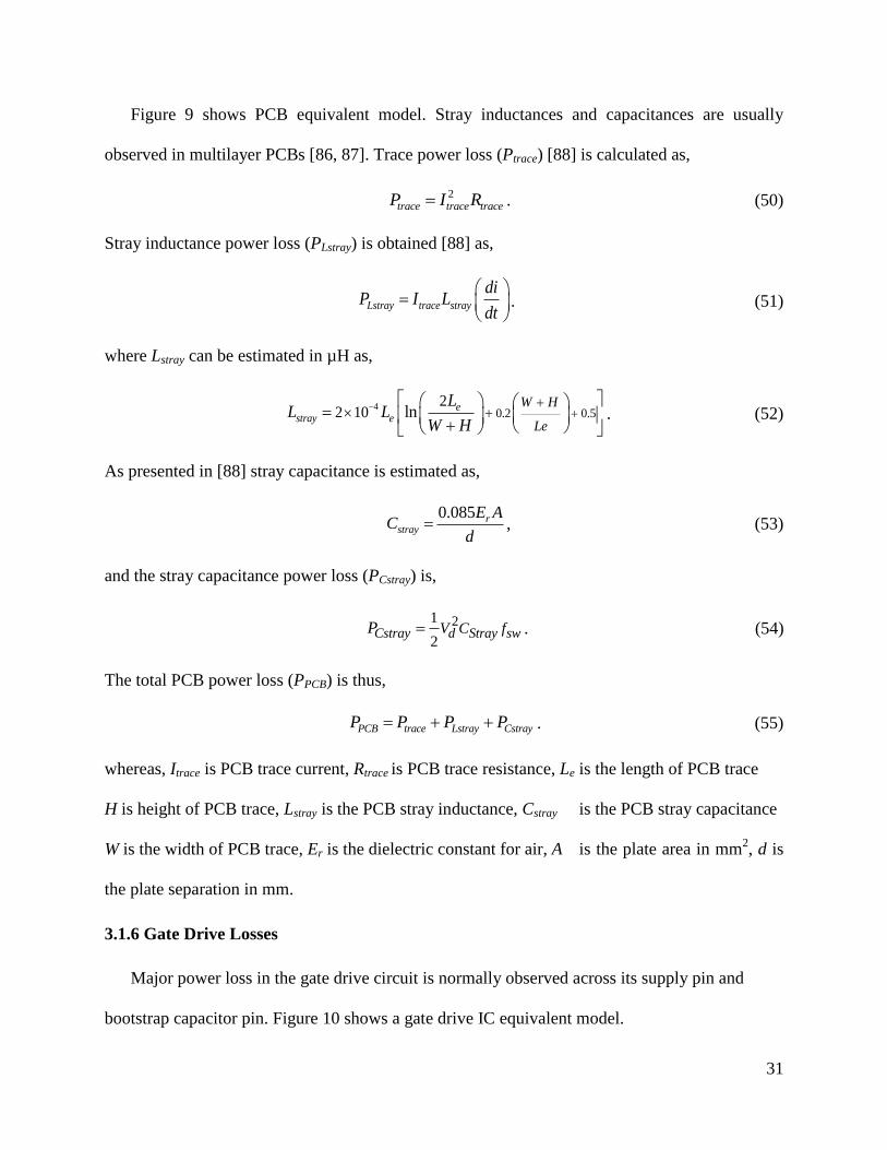
Figure 9 shows PCB equivalent model. Stray inductances and capacitances are usually
observed in multilayer PCBs [86, 87]. Trace power loss (Ptrace) [88] is calculated as,
2trace trace traceP I R . (50)
Stray inductance power loss (PLstray) is obtained [88] as,
Lstray trace stray
diP I L
dt
. (51)
where Lstray can be estimated in µH as,
40.2 0.5
22 10 ln e
stray e
W H
Le
LL L
W H
. (52)
As presented in [88] stray capacitance is estimated as,
0.085 rstray
E AC
d , (53)
and the stray capacitance power loss (PCstray) is,
21
2Cstray d Stray swV C fP .
(54)
The total PCB power loss (PPCB) is thus,
PCB trace Lstray CstrayP P P P . (55)
whereas, Itrace is PCB trace current, Rtrace is PCB trace resistance, Le is the length of PCB trace
H is height of PCB trace, Lstray is the PCB stray inductance, Cstray is the PCB stray capacitance
W is the width of PCB trace, Er is the dielectric constant for air, A is the plate area in mm2, d is
the plate separation in mm.
3.1.6 Gate Drive Losses
Major power loss in the gate drive circuit is normally observed across its supply pin and
bootstrap capacitor pin. Figure 10 shows a gate drive IC equivalent model.

32
Gate drive losses shown in this paper mainly focused on self-oscillating ICs or dedicated
application ICs
Gate
Driver IC
CB
VBT
+
-
VCC
+
-
IQBS
IQCC
Figure 10 Gate drive ICs equivalent model
Gate drive power loss (PGDRV) is calculated as in [89] to be,
GDRV VCC BTP P P , (56)
where , VCC QCC CCP I V , (57)
BT QBS BTP I V . (58)
whereas, IQBS, IQCC is the gate drive quiescent currents, VCC is gate drive IC supply voltage, VBT
is the gate drive IC bootstrap voltage. The converter total power loss (PTotal) is thus:
Total ( ) ( ) ( ) ( )P P P P P P P
loss MOSFET loss Inductor loss Diode loss Capacitor PCB GDRV (59)
3.2 Power Loss Models for Several Converters
Equations explained in the previous section are common in the literature but are rarely
presented for specific converter topologies. In this section, power loss models for boost and buck
converter in CCM and flyback converter in DCM are explained in detail. These converters are
used as examples due to their common use in any applications and their simple construction and
analysis. All generalized equations are reformulated in terms of input and output parameters and
datasheet information.
When power loss equations for a specific converter are prepared, some approximations are
made, such as when MOSFET switching power losses in the boost converter are calculated, drain

33
to source voltage is assumed as Vin only. Ideally, while calculating drain to source voltage VDS,
the voltage across inductor VL should be subtracted from input voltage Vin. However, since
inductor contributes almost zero power loss in switching losses of the MOSFET, it can be
excluded from measurement of MOSFET switching power loss. When the diode switching loss
in the buck converter is calculated, the power loss across ESR is not considered. In Figure 12, the
flyback transformer’s primary current waveform is assumed to be linear, but sometimes it is
exponential. Similarly, the flyback inductor switching waveform as shown in Figure 13 excludes
the exponential region and the effect of disturbances on the linear region. These generalized
assumptions are made because their effects on power loss models are insignificant and they
cannot reduce the source of error in the estimated and the measured power losses.
3.2.1 Boost Converter in CCM
A typical non-ideal boost converter is shown in Figure 11. Derivations for boost converter in
CCM are as follows,
Figure 11 Boost converter with its non-idealities
3.2.1.1 MOSFETs Losses
PCM is obtained from (31) and can be estimated [90,91] as,
22
12CM DSon in
iP R D I
. (60)

34
To calculate PSW, IDon and IDoff can be obtained from Figure 7,
2Don in
iI I
,
(61)
2Doff in
iI I
,
(62)
DS inV V .
(63)
Thus, PON(M) and POFF(M) are calculated as,
(M)
1
2 2ON in in r sw
iP V I t f
, (64)
(M)
1
2 2OFF in in f sw
iP V I t f
. (65)
whereas, Vin is the converter input voltage, Δi is the inductor ripple current, Iin is the converter
input current, VDS is the drain-to-source voltage, Vout is the converter output voltage and Iout is the
converter output current and VF is the diode forward voltage.
3.2.1.2 Diode Losses
PCD and PSWD are obtained by referring (37) and (40) as,
20(1 ) (1 )CD D in D inP V D I R D I , (66)
1
2SWD rr out in in swP Q V V I DCR f . (67)
3.2.1.3 Inductor Losses
PCORE, PDCR and PACR can be calculated as,
2
out in in F
CORE
C
V V I DCR VP
R
, (68)
2DCR inP I DCR ,
(69)

35
2
12ACR
iP ACR
. (70)
3.2.1.4 Capacitor Losses
Ploss (Capacitor) is obtained using (47) and Figure 8 as,
2
( )12
loss Capacitor
iP ESR
.
(71)
3.2.2 Buck Converter in CCM
A typical non-ideal buck converter is shown in Figure 12. Buck converter in CCM operation
is considered for the following derivations:
Figure 12 Buck converter topology for power loss model
3.2.2.1 MOSFETs Losses
PCM is obtained from (31) and can be estimated from [91] as,
22
12CM DSon out
iP R D I
, (72)
To calculate PSW, IDon and IDoff can be obtained from figure 7 and VDS is as (63) .Thus, PON and
POFF are obtained as,
2Don out
iI I
,
(73)
2Doff out
iI I
,
(74)

36
(M)
1
2 2ON in out r sw
iP V I t f
, (75)
(M)
1
2 2OFF in out f sw
iP V I t f
. (76)
3.2.2.2 Diode Losses
PCD and PSWD are obtained by referring (37) and (40) as,
20(1 ) (1 )CD D out D outP V D I R D I , (77)
1
2SWD rr out out swP Q V I DCR f . (78)
3.2.2.3 Inductor Losses
PCORE, PDCR and PACR can be calculated as,
2
in out in DSon out
CORE
C
V V I R I DCRP
R
, (79)
2DCR outP I DCR , (80)
2
12ACR
iP ACR
. (81)
3.2.2.4 Capacitor Losses
Ploss (Capacitor) is obtained using (47) and Figure 8 as,
2
( )12
loss Capacitor
iP ESR
.
(82)
3.2.3 Flyback converter in DCM
Flyback converters are widely used in DCM. A non-ideal flyback converter in DCM is
shown in the Figure 13.

37
Figure 13 Flyback converter model with its non-idealities
3.2.3.1 MOSFET Losses
For this application MOSFET switching period was considered as TON+TOFF=0.8TS. MOSFET
switching waveform is shown in Figure 14.
Figure 14 MOSFET switching waveform
Since, 0.8 S out F
ON
F
T V VT
V
,
(83)
DS in outV V nV ,
(84)
PCM in the flyback converter is described in [91, 92] as,
2
0.26 1in outCM DSon
Fm pri sw
V VP R D
VL L f
. (85)
For a flyback converter in DCM, IDon is zero but IDoff and PSW are determined using [93, 94] and
Figure 15 as,
2
0.9
m pri sw
inDoff
L L f
V DI
, (86)
Δi
ILavg
TON TOFF
TS
Td
ILpkID
Time

38
(M)
22
0.9
m pri
finSW OFF in out
L L
tV DP P V nV
. (87)
Figure 15 Inductor switching waveform
whereas, Lm is the mutual inductance, Lpri is the primary inductance, Lsec is the secondary
inductance.
3.2.3.2 Diode Losses
PCD and PSWD of the flyback diode are calculated as,
2
0
0.52(1 ) (1 )
m pri
inCD D out D
swL L
nV DP V D I R D
f
, (88)
1
2SWD rr out swP Q V f .
(89)
3.2.3.3 Flyback Coupled-Inductor/Transformer Lossses
PCORE is given in [92-94] as,
CORE fe AC C mP K B A L . (90)
where,
Pr
mAC
i C
L iB
N A
.
(91)
Primary and secondary resistive losses are calculated [94] as,
2
0.4
m pri sw
inRpri pri
L L f
V DP R
, (92)
ΔiILavg
TON TOFF
TS
Td
Ipk
Time
IL

39
2
sec sec
0.4
m pri sw
inR
L L f
nV DP R
. (93)
In these equations, AC is the cross-sectional area of core, BβAC is the AC component of flux
density, Kfe is the inductor current material constant at switching frequency, Npri is the primary
windings number of turns, PRpri is the primary resistance loss, PRsec is the secondary resistance
loss, Rpri is the primary DC resistance and Rsec is the secondary DC résistance.
3.2.3.4 Capacitor Losses
From (48), Ploss (Capacitor) is calculated as,
2
2( )
0.52
m pri
inloss Capacitor out
swL L
nV DP I ESR
f
. (94)
3.2.3.5 Snubber Circuit Losses
The main components in the snubber branch are snubber resistor (Rsn), snubber capacitor Csn and
snubber diode (Dsn). Rsn and Csn form a clamp unit. Power loss in the clamp unit (Pclamp) is
represented in [95] as,
2 2
0.9clamp DSBR in
clamp
sn sn
V V VP
R R
,
(95)
Pclamp is also written as,
21
21
0.9 2
inclamp sw pri
DSBR in
f LV
P iV V
. (96)
Snubber diode conduction loss (PCDsn) is obtained from (41) as,
20(1 ) (1 )CDsn Dsn out Dsn SrmsP V D nI R D nI . (97)
Snubber diode switching loss (PSWDsn) is obtained as,
1
2SWDsn rrsn in swP Q V f .
(98)

40
whereas, Rsn is the snubber resistor, RDsn is the snubber diode on-state resistance, VDSBR is the
drain-to-source breakdown voltage, Vclamp is the clamp voltage rise, ISrms is the flyback
transformer secondary RMS current, VDsn0 is the snubber diode initial state voltage, Qrrsn is the
snubber diode reverse recovery charge, IDsn(rms) is snubber diode RMS current and IDsn(avg) is
snubber diode avg. current
Total snubber circuit power loss (Psn) is represented as,
sn clamp CDsn SWDsnP P P P .
(99)
3.3 Results
Basic boost, buck and flyback converters were experimentally developed to test the power
loss models presented here. These converters were tested in open-loop mode. All parasitic
elements and specific test condition examples are given in Table I. Figure 16 shows the board
holding both the boost and buck converters. However, gate drive circuits are not powered from
Vin thus their losses are not included. In addition to assumptions listed in sections 3.1 and 3.2,
some approximations are made for testing these converters, e.g. RC (when not given in a
datasheet), and limited measurement accuracy. Each converter and its related results and
waveforms are presented and discussed separately. In this section, detailed converter
specification, each component power loss and specific converter power losses are organized.
Measured power losses are calculated as the difference between measured input and output
powers as recorded on the oscilloscope.

41
Figure 16 Experimental setup for the buck and boost converters
Table I Example testing conditions and parasitic elements in experimental prototypes
Parameter Boost Buck Flyback
Vin 20V 62V 11.2V
Iin 3.5A 1.1A 0.38A
Vout 77.4V 24.6V 19.6V
Iout 0.85A 2.56A 0.15A
Δi 1.1A 2.95A 0.89A
fsw 50KHz 50KHz 100KHz
D 0.75 0.4 0.5
ESR 0.603Ω 0.603Ω 0.603Ω
VD0 1V 1V 1V
RD 7mΩ 7mΩ 7mΩ
DCR/Rpri 0.06Ω 34mΩ 0.09
ACR/Rsec 0 1.5Ω 0.58
Qrr 195nC 195nC 195nC
Qgs 64nC 13nC 13nC
RDSon 0.029Ω 0.18Ω 0.18Ω
tr 100nsec 51nsec 51nsec
tf 63nsec 36nsec 36nsec
≈ Rcore 3325Ω - -
Lm, Lpri - - 59.4µH
3.5µH B - 3400mT 42.42mT
Ve/AC - 0.24cm3 0.97cm
3

42
3.3.1 Boost Converter Results
Basic boost converter topology is built as shown in Figure 11 and operates in CCM. Table II
explains boost converter results for different duty ratios along with actual measurements using a
resistive load. Accuracy of the estimated power loss exceeds 92% with less than +/-8%
estimation error. Table II represents the components, estimated and measured power losses.
Table III presents detailed boost converter component power losses for different duty ratios. For
the boost converter operation MOSFET-IRFP4332PBF, inductor-PCV-0-274-10L, diode-
MURF860G and capacitor-EEU-EB2D221 are used. Inductor and capacitor values are selected
from the rapid prototyping tool selection procedure for the boost converter as will be explained
in Section 5.2.1.1 Figures 17-21 demonstrate operation of the boost converter from a 30% duty
ratio to a 75% duty ratio. It is observed from Figure 17-21 that as duty ratio increases system
performance decreases. The boost converter provides almost ideal performance at the 50% duty
ratio but this is a drawback of the V-I measurement method [97] and oscilloscope which cannot
capture the accurate results for higher disturbances. Measured power loss (Pmeasured) and
estimated power loss (Pestimated) can provide percentage error. Estimation error shown in Table II
and later tables is calculated as,
measured estimated
measured
P - P% Error = ×100
P
. (100)
Table II Estimated and measured power loss in boost converter
Duty
Ratio
PMeasured
(W)
PEstimated
(W)
%Error
30% 0.6 0.56 6.6%
40% 0.78 0.72 7.69%
50% 0.97 0.92 5.15%
60% 1.36 1.37 -0.74%
75% 4.21 4.19 0.43%

43
Table III Detailed boost converter component power losses for different duty ratios
Parameters Duty Ratios
30% 40% 50% 60% 75%
Vin 20 20 20.1 20 20
Iin 0.45 0.6 0.88 1.35 3.50
Vout 28 33 39.8 49.3 77.4
Iout 0.3 0.34 0.42 0.52 0.85
fsw 50KHz 50KHz 50KHz 50KHz 50KHz
D 0.3 0.4 0.5 0.6 0.75
PMeasured 0.6 0.78 0.97 1.36 4.21
Ploss_Mosfet 0.10 0.11 0.14 0.19 0.61
Ploss_Diode 0.4 0.5 0.54 0.69 1.18
Ploss_Inductor 0.03 0.06 0.15 0.34 1.67
Ploss_Capacitor 0.01 0.02 0.03 0.04 0.062
PPCB 0.02 0.03 0.06 0.1 0.67
PEstimated 0.56 0.72 0.92 1.37 4.19
%Error 6.6 7.69 5.15 -0.74 0.43
Figure 17 Boost converter results for 30% duty
Vout (50V/div)
Vin (50V/div)
Iout (0.5A/div)
Iin (1A/div)

44
Figure 18 Boost converter results for 40% duty ratio
Figure 19 Boost converter results for 50% duty ratio
Figure 20 Boost converter results for 60% duty ratio
Vout (50V/div)
Vin (50V/div)
Iout (0.5A/div)
Iin (1A/div)
Vout (50V/div)
Vin (50V/div)
Iout (0.5A/div)
Iin (1A/div)
Vout (50V/div)
Vin (50V/div)
Iout (0.5A/div)
Iin (1A/div)

45
Figure 21 Boost converter results for 75% duty ratio
3.3.2 Buck Converter Results
The basic buck converter topology is built as shown in Figure 12 and operates in CCM.
Table IV explains buck converter results for different duty ratios with actual measurements from
an oscilloscope and the estimated power loss from the power loss model of the buck converter.
The error between the measured power loss and the estimated power loss is less than 8%. Table
IV represents components, estimated and measured power losses and Table V presents detailed
buck converter component power losses for different duty ratios. For buck converter operation
MOSFET- IRFP4332PBF, Inductor- AIRD-03-101k, Diode-MURF860G and capacitor- EEU-
EB2D221 are used based on the component selection that will be described in Section 5.2.1.1.
Figures 22-25 demonstrate operation of the buck converter from a 20% duty ratio to a 50% duty
ratio.
Table IV. Estimated and measured power loss in buck converter
Duty
Ratio
PMeasured
(W)
PEstimated
(W)
%Error
20% 2.54 2.49 -1.96%
30% 3.76 3.78 0.53%
40% 5.22 5.20 -0.45%
50% 7.05 6.55 -7.09%
Vout (50V/div)
Vin (50V/div)
Iout (0.5A/div)
Iin (1A/div)

46
Table V Detailed buck converter component power losses for different duty ratios
Parameters Duty Ratios
20% 30% 40% 50% 60%
Vin 60 60 62 61 46
Iin 0.28 0.6 1.1 1.65 1.6
Vout 12.4 18 24.6 30 27.1
Iout 1.15 1.79 2.56 3.12 2.55
fsw 50KHz 50KHz 50KHz 50KHz 50KHz
D 0.2 0.3 0.4 0.5 0.6
PMeasured 2.54 3.76 5.22 7.05 4.49
Ploss_Mosfet 0.23 0.45 0.87 1.36 1.01
Ploss_Diode 0.99 1.36 1.68 1.74 1.17
Ploss_Inductor 0.95 1.31 1.51 1.87 1.22
Ploss_Capacitor 0.20 0.32 0.44 0.45 0.24
PPCB 0.13 0.19 0.70 1.13 0.83
PEstimated 2.49 3.78 5.2 6.55 4.47
%Error -1.96 0.52 -1.09 -7.09 -0.45
Figure 22 Buck converter results for 20% duty ratio
Vout (50V/div)
Vin (50V/div)
Iout (2A/div)
Iin (1A/div)

47
Figure 23 Buck converter results for 30% duty ratio
Figure 24. Buck converter results for 40% duty ratio
Figure 25 Buck converter results for 50% duty ratio
Vout (50V/div)
Vin (50V/div)
Iout (2A/div)
Iin (1A/div)
Vout (50V/div)
Vin (50V/div)
Iout (2A/div)
Iin (1A/div)
Vout (50V/div)
Vin (50V/div)
Iout (2A/div)
Iin (1A/div)

48
3.3.3 Flyback Converter Results
Basic flyback converter topology is built as shown in Figure 13 and operates in DCM
Flyback converter results for different duty ratios are shown in Table VI with actual
measurements from an oscilloscope and the estimated power loss from the power loss model of
the flyback converter. The error between the measured power loss and the estimated power loss
is less than 5%. Table VII represents components, estimated and measured power losses and
Table VII presents detailed flyback converter component power losses for different duty ratios.
For flyback converter operation MOSFET-IRFP4332PBF, flyback transformer-Q4338-BL,
Diode-EGP10G and capacitor-EEU-EB2D221 are used. Figures 26-29 demonstrate operation of
the flyback converter from a 20% duty ratio to a 50% duty ratio that is maximum duty ratio.
Table VI. Estimated & measured power loss in flyback converter
Duty Ratio PMeasured
(W)
PEstimated
(W)
%Error
20% 0.32 0.31 -3.13%
30% 0.55 0.56 1.81%
40% 0.85 0.82 -4.7%
50% 1.32 1.27 -3.78%
Table VII Detailed flyback converter component power losses for different duty ratios
Parameters Duty Ratios
20% 30% 40% 50%
Vin 11.7 11.6 11.6 11.2
Iin 0.075 0.2 0.2 0.38
Vout 9.26 11.1 14.7 19.6
Iout 0.06 0.16 0.1 0.15
fsw 100KHz 100KHz 100KHz 100KHz
D 0.2 0.3 0.4 0.5
PMeasured 0.32 0.55 0.85 1.32
Ploss_Mosfet 0.08 0.16 0.32 0.58
Ploss_Diode 0.14 0.22 0.20 0.27
Ploss_Inductor 0.03 0.05 0.07 0.09
Ploss_Capacitor 0.02 0.02 0.06 0.08
Psn 0.04 0.10 0.14 0.21
PPCB 0.004 0.01 0.02 0.04
PEstimated 0.31 0.56 0.81 1.27
%Error -3.13% 1.81% -4.7% -3.78

49
Figure 26 Flyback converter results for 20% duty ratio
Figure 27 Flyback converter results for 30% duty ratio
Figure 28 Flyback converter results for 40% duty ratio
Vout (50V/div)
Vin (50V/div)
Iout (2A/div)
Iin (1A/div)
Vout (50V/div)
Vin (50V/div)
Iout (2A/div)
Iin (1A/div)
Vout (50V/div)
Vin (50V/div)
Iout (2A/div)
Iin (1A/div)

50
Figure 29. Flyback converter results for 50% duty ratio
Overall, results in Tables II, IV and VI are shown to be within 8% error and thus the power
loss models established are proven to be more than 92% accurate. The accuracy of the power
loss model is improved by considering the power loss of each component along with its non-
idealities and parasitic elements. The estimation of PCB losses has also helped to improve the
accuracy. The power loss model can be further improved if power loss of each component of the
converter is estimated. This power loss model can also be developed for other components,
converter topologies and systems with the same approach. Furthermore, power loss models for
microcontrollers and DSP ICs can also improve accuracy and flexibility. Component power
losses for each converter are provided in the Appendix I. Detailed derivation of RMS values of
drain currents, capacitor RMS current of the flyback converter and inductor currents are given in
the Appendix III.
Vout (50V/div)
Vin (50V/div)
Iout (2A/div)
Iin (1A/div)

51
CHAPTER 4: COST MODELS FOR CONVERTERS
The principal function and ultimate aim of industry is to make profitable products. Today’s
marketplace is full of new products and services changing at a very fast pace. In order to stay
competitive in a rapidly changing consumer market, companies must focus on value generation
for their customers. This value can be generated through new features and better functionality at
lower costs. Cost has emerged as one of the most important attributes of a successful product and
of a competitive industry in general.
When industry develops a new product with the customers’ requirements in mind, the
product has to go through numerous designs, engineering, manufacturing, testing and compliance
procedures. All these factors contribute to the product cost and are indispensable to product
success. While industry cannot avoid these critical operations in order to reduce cost, it still must
remain focused on constantly lowering the cost while maintaining the product quality, reliability
and availability at a high level. Developing prudent and practical cost reduction techniques based
on raw material prices is thus a vital focus area for product designers and engineers.
In the particular case of electronics components, cost forms a major decision making factor.
High-end electronics is an extremely competitive market and customer preferences are pushing
developments towards more functionality at progressively lower cost. With the ever rising
demand and constant cost pressure, it has become vitally important for electronic components to
be designed and manufactured more efficiently and at lower costs.
The cost model developed in this research aims at solving this very important challenge
facing a design engineer. These models are based on average prices related to component ratings
obtained using an extensive market survey and surface-fitting tools. A large database of cost
information for different elements was collected from common manufacturers and suppliers.

52
Average cost for each component at a certain rating combination was found by considering
multiple options. This database was input to MATLAB to create an interpolated graph and the
MATLAB surface fitting and the curve fitting tools were used to find a mathematical
relationship between cost and component parameters. Cost per quantity was considered to avoid
price discrepancy between manufacturers, purchase quantities, etc. It is important to note that
component technology and cost profiles change over time as a result of changes in material and
manufacturing techniques, but the methodology proposed here still applies.
In this chapter, sections 4.1-4.4 show cost models developed for MOSFETs, diodes,
inductors, and capacitors, respectively. Section 4.5 elaborates on the importance of magnetic
core cost estimation and shows the proposed core cost model. Section 4.6 discusses the cost
model for magnet wire which is also critical to inductor and transformer design. Section 4.7
shows real against estimated prices of various components to validate the developed cost models.
4.1 MOSFET Cost Model
MOSFET selection procedure is based on its drain-to-source voltage, drain current, gate-to-
source threshold voltage and switching time. These parameters decide the performance and the
efficiency of the circuit. However, when the MOSFET is selected to develop any power
electronic converter, its worst case current and voltage stress handling capacity has to be
analyzed. Thus, to create a cost model equation for the MOSFET, a large database was prepared
using drain to source voltage VDS, drain current ID and cost.
Figures 30 and 31 depict the mathematical relationship for this database as applicable to
single as well as 1000 quantities. Cost per quantity is considered because the prices fluctuate
with changing quantities. It can be observed that the structure of these two figures is almost
identical. This indicates that even if this approach is implemented for different values of

53
quantity, the cost model equation from the surface fitting tool remains the same. Thus, the
MOSFET cost model equation for multiple quantities (CostM) is represented as,
13
0
( , )i
i iM DS D i DS D
i
Cost V I V I
,
(101)
Table VIII. αi Coefficients and ranges
Coefficient Values Ranges βi γi
α0 1.622 (-9.142, 12.39) 0 0
α 1 0.034 (-0.087, 0.154) 1 0
α 2 -0.133 (-0.89, 0.63) 0 1
α 3 -0.0001 (-8, 25) 2 0
α 4 -0.0016 (-0.0047,-0.0163) 1 1
α 5 0.0058 (-0.01, 0.022) 0 2
α 6 1.3e-8
(-1.6e-6,1.6e-6) 3 0
α 7 8e-6 (-8.8e-7, 1.5e-5) 2 1
α 8 -2.95e-6 (-4.2e-5,3.6e-5) 1 2
α 9 -4.48e-5 (-1.4e-5,5.3e-5) 0 3
α 10 1.46e-10 (-1.2e-9,1.5e-9) 4 0
α 11 -5.3e-9 (-1.1e-8,5.6e-10) 3 1
α 12 -3.5e-8 (-6.9e-8, 1.3e-9) 2 2
α 13 1.3e-7 (-8.1e-8,3.4e-7) 1 3
In equation 101, CostM is MOSFET cost, VDS is MOSFET drain-to-source voltage, ID is MOSFET
drain-to-source current. αi values are obtained from the surface fitting tool. Table VIII represents
different αi values and their ranges. To calculate exact cost αi values must be varied within the
specified range. These coefficients cannot change as per the quantity making this equation
suitable for use with multiple quantities.

54
Figure 30 MOSFET cost model for one unit
Figure 31 MOSFET cost model for 1000 units
4.2 Diode Cost Model
As described in the power loss model, it is necessary to analyze performance of a diode in
‘ON’ state as well as in ‘OFF’ state because when the diode is ‘ON’ it provides inductor current
to the load and when it is ‘OFF’ it blocks reverse voltage from the load. When selecting a diode
0200
400600
0
50
100
1500
10
20
30
VDS
(V)ID
(A)
Cost
M($
)
0200
400600
050
100150
0
10
20
VDS
(V)ID
(A)
Co
stM
($)

55
for a power electronic converter, designers have to consider the ability of Diode to block the
reverse voltage, capacity to handle peak current, forward voltage drop and the switching
operation time. Out of these conditions, diode’s selection procedure is mainly concerned with its
reverse blocking voltage and its current capacity. With this consideration cost model equation for
a diode was derived using DC blocking voltage (VB), diode forward current (IF) and the diode
cost (CostD). Interpolated graphs of diodes for single and 1000 quantities are presented in Figure
32 and 33, respectively. These two interpolated graphs are almost identical thus establishing that
cost model equation is independent of quantities.
The diode cost (CostD) is represented as,
2
0
( , )
jj j
D B F j B F
j
Cost V I V I
.
(102)
Where δ coefficients are obtained as,
Table IX δj coefficients for diode cost model equations
Coefficients Value Range j
κj
δ0
0.22
(-0.1, 0.3)
0 0 δ 1
7e-5
(-2.6e-4, 1.2e-4)
0 1 δ 2
0.1
(-0.08, 0.13)
1 0
In this equation δj values are obtained from surface fitting tool. Different δ values and their
ranges are presented in Table IX. To calculate exact cost the δ values must be varied within the
specified range. These coefficients cannot change as per the quantity so this equation can be used
for multiple quantities.

56
Figure 32 Diode cost model for one unit
Figure 33 Diode cost model for 1000 units
0
500
1000
0
5
100
0.5
1
1.5
VB (V)
IF (A)
Cost
D($
)
0
500
1000
0
5
100
0.5
1
VB
(V)IF (A)
Cost
D (
$)

57
4.3 Inductor Cost Model
Similar to the MOSFET and diode, an inductor also plays a vital role in the operation of the
converter. Moreover, it is the value of the inductance that decides modes of operation for the
converter. A smaller value of inductance results in failure of the inductor to operate in a specific
mode whereas a higher value increases the start-up and settling times. The cost of an inductor is
sometimes higher than that of other components in a converter. Designers may even opt to select
the cores and the magnet wires to prepare an inductor as per the application requirement, but the
cost model developed in this section is only for the ready-made inductors which are readily
available in the market. Cost model for the inductors is based on inductance (L), inductor current
(IL) and cost as shown in Figures 34 and 35. Interpolated graphs are almost identical for single as
well as multiple quantities. The inductor cost (CostL) is represented as,
2( )( , ) sin( )
ILL L LCost L I LI e
, (103)
Table X Inductor cost model coefficients
Coefficients Value Ranges
x 9.67 (-3.48, 24.83)
µ 61.64 (-25.68, 97.59)
-8.246 (-20.63, 8.141)
v 4.495 (-0.2334, 9.223)
ω -0.08658 (-0.5143, 0.3411)
In Table X, the inductor cost model coefficients are obtained from surface fitting tool. These
coefficients do not change as per the quantity so this equation can be used for multiple quantities.
Similar approach can be implemented on the cores and magnet wires for the inductors. The cost
models for flyback transformer cores and magnetic wires are based on this approach.
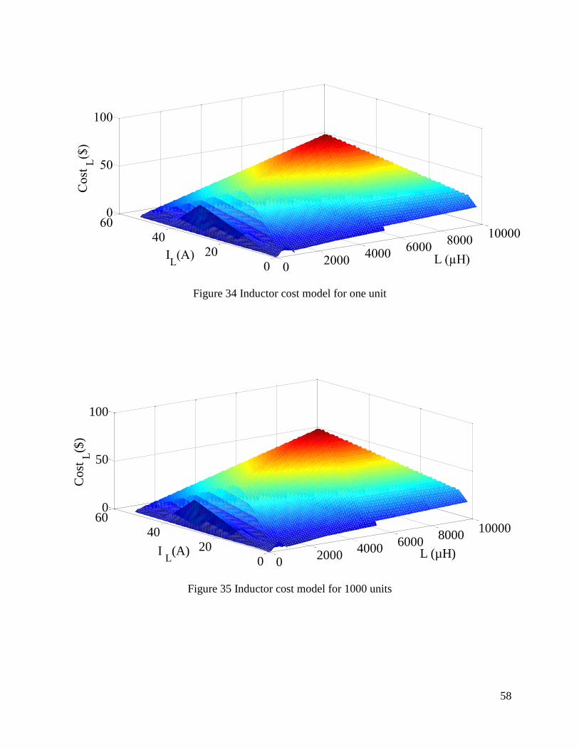
58
Figure 34 Inductor cost model for one unit
Figure 35 Inductor cost model for 1000 units
02000
40006000
800010000
020
40600
50
100
L (µH)IL
(A)
Co
st L
($)
02000
40006000
800010000
020
4060
0
50
100
L (µH)I L(A)
Co
st L
($)

59
4.4 Capacitor Cost Model
A capacitor acts as a filter which is predominantly selected to suppress output voltage ripple
and to handle output current ripples in the converter. As described in the previous section,
capacitor power loss is dependent upon the ESR value. Thus, while selecting a capacitor for the
converter, designers have to consider its capacitance value, capacity of handling the output
voltage ripples and the ESR value.
In this cost model, a database was prepared for capacitance value (C), capacitor voltage (VC)
and the corresponding cost. Figures 36 and 37 show the interpolated graphs which are prepared
from the capacitor database and the mathematical relationship for these graphs is also presented
here.The capacitor cost (CostC) is represented as,
8
0
( , )z
zzC C z C
z
Cost C V C V
,
(104)
Table XI. ηz coefficients and ranges
Coefficients Value Ranges z ξz
η0 -0.5651 (-4.043, 2.913) 0 0
η 1 7.98e-4 (-0.017, 0.019) 1 0
η 2 0.03 (-0.022, 0.082) 0 1
η 3 5.1e-6 (-1.6e-5,1.74e-53) 2 0
η 4 3.2e-5 (-5e-5, 0.0001139) 1 1
η 5 -1.8e-4 (-4e-4,5.9e-5) 0 2
η 6 -4.9e-8 (-1.1e-7,1e-8) 2 1
η 7 1.6e-7 (4.2e-8,2.8e-7) 1 2
η 8 2.5e-7 (-5.5e-8, 5.6e-8) 0 3
Equation 104 represents the cost equation for capacitors, where Table XI presents the ηz
coefficients obtained from MATLAB surface fitting tool. These coefficients are not affected by
changes in quantity so this equation can be used for multiple quantities.

60
Figure 36 Capacitor cost model for one unit
Figure 37 Capacitor cost model for 1000 units
0200
400600
8001000
0
200
400
6000
10
20
30
40
C (µF)V C
(V)
Co
st C
($)
0200
400600
8001000
0200
400600
0
10
20
30
C (µF)VC
(V)
Cost
C (
$)

61
4.5 Cost Model for Flyback Coupled-Inductor/Transformer Cores
Cores are vital elements when designing a flyback coupled inductor or transformer. They
decide the mode of operation, performance and efficiency of a converter. Some manufacturers
provide ready flyback transformers for commonly used applications, but even these commonly
stem from custom designs. . There are two types of cores i.e. gapped and ungapped. In this cost
model both these types are considered. Frequency range considered for the cores is 50 KHz to
500 KHz, and high frequency cores which are used for radio or telecommunications application
are excluded from this research. Figures 38 and 39 show interpolated graph for core database.
Cost model for the core is obtained on the basis of inductance factor value (AL), switching
frequency (fsw) and cost. AL value is considered because the inductance value is directly
proportional to AL. The core cost (CostCo) is represented as,
4( , )
0
m mm
Cost A f A fCo L sw m L sw
m
, (105)
Table XII τm Coefficients and ranges
Coefficient
s
Value Ranges m m τ0 1.204 (0.6736, 1.735) 0 0
τ1 1.625
(1.31, 1.939) 1 0
τ2 0.1432 (-0.6245, 0.9078) 0 1
τ3 -0.007604 (-0.467, 0.4518) 1 1
τ4 -0.1744 (-0.6827, 0.344) 0 2
Equation 105 represents the cost equation for the cores where τm coefficients obtained from
MATLAB surface fitting tool are presented in Table XII. These coefficients are unchanged with
respect to quantity so this equation can be used for multiple quantities.

62
Figure 38 Flyback core cost model for one unit
Figure 39 Flyback core cost model for 1000 units
05000
1000015000
0
200
400
6000
5
10
AL (nH)f
sw (KHz)
Cost
Co (
$)
05000
1000015000
0
200
400
6000
5
10
AL (nH)f
sw (KHz)
Cost
Co (
$)

63
4.6 Magnet Wire Cost Model
Magnet wire decides the current range of the flyback coupled inductor or transformer.
Magnet wires are selected as per the gauge and total bundle cost where current requirement for a
specific gauge is provided by the manufacturers. For the purpose of this section only a two
dimensional graph is created to estimate cost equation since current and wire gauge are already
established by standards for heat dissipation and safety. Table XIII described current requirement
for specific gauge. The wire gauge and its corresponding current capacity are obtained from [83].
Table XIII Wire gauge and its current capacity [83]
Wire Gauge Current Capacity
10 13.84
12 8.71
14 5.48
16 3.44
18 2.17
20 1.36
22 0.86
24 0.54
26 0.34
28 0.21
30 0.13
32 0.084
34 0.05
36 0.033
38 0.021
40 0.0132
Figure 40 shows magnet wire gauge (G) vs. cost graph where the cost model given here is
developed for half pound bundles for consistency purposes. Cost equation for the magnet wire is
obtained from the curve fitting tool .The capacitor cost (CostW) is represented as,
6
0
(G)
w q
q
Cost G
,
(106)

64
Table XIV φq coefficients and ranges
Coefficient
s
Value Ranges ςq
φ0 0.0002906 (0.6736, 1.735) 5
φ 1 -0.03452
(1.31, 1.939) 4
φ 2 1.608 (-0.6245,
0.9078)
3
φ 3 -36.42 (0.5611, 1.106) 2
φ 4 396.6 (-0.467, 0.4518) 1
φ 5 -1583 (-0.6827, 0.344) 0
Equation (106) represents cost equation for the magnet wire where φq coefficients as presented in
Table XIV are obtained using the MATLAB curve fitting tool. This equation is independent of
quantities since the related coefficients do not vary with quantity.
Figure 40 Magnet wire cost model for single bundle
Thus various cost models are prepared for estimating the cost of components and they can
easily be extended for the purpose of system level cost estimation. Results are presented in the
next section and are shown to be 90% accurate. The equation forms provided in section 4.1-4.6
were selected based on R2 values as shown in Appendix IV. Next section includes a detailed
analysis of results for the cost estimation of each component considered in this section.
10 15 20 25 30 35 400
50
100
150
200
G (AWG)
Co
st (
$)

65
4.7 Cost Models Results
A cost database for basic components was developed to test the cost models presented
here.The cost estimates of components which are used for actual experiment are compared with
actual prices from suppliers. Table XV summarizes components which are used for boost, buck
and flyback converter development. The actual cost (Costactual) and the estimated cost
(Costestimated) can provide percentage error. The error obtained from actual and estimated cost is
shown as,
actual estimated
actual
C - C% Error = ×100
C
(107)
Table XV. Detailed cost comparison for power components
Component Cactual Cestimated % Error
MOSFET-FP4332PBF $4.33 $4.37 -0.92%
Inductor-AIRD-03-101K $5.97 $5.95 0.33%
Diode- MURF860G $0.99 $1.03 -4.04%
Capacitor-220µF/250V $0.723 $0.752 -4.01%
Core- B66421G0000X187 $0.69 $0.724 -4.93%
Wire-Belden wire 8051,
22AWG
$49.03 $48.03 2.039%
Results in Table XV are shown to have less than 5% error and thus the cost models
established prove that the results are more than 95% accurate. The accuracy of the cost model
was improved with the help of interpolated graphs and surface fitting tools. An accurate surface
fit can give better results of the interpolated graphs. Exact cost of the component can be obtained
if coefficients are changed within specified range. The MATLAB surface fitting tools cannot
provide exact surface fits but they can provide surface fitting estimates to some extent. Cost of
the component changes as per trend and changes in technology and web based cost model can
estimate component costs considering these changes. The cost model presented here can find
‘Ceiling cost’, that is the maximum cost of the component. Further improvement has to be made

66
in the cost model such that it can estimate a ‘Floor Cost’, that is the minimum cost of a
component. This can be achieved if database of all available and active components is obtained
from the manufacturers and distributors. Furthermore, a web based cost model can be developed
following the approach presented here and an active database of manufacturer and distributor
data can be incorporated into it to provide a robust, flexible and scalable cost modeling tool.

67
CHAPTER 5: RAPID PROTOTYPING TOOLS FOR POWER LOSS AND COST MODELS
Rapid prototyping is of interest for research, industrial, and commercial purposes as a major
time and cost saving tool. Many engineers, researchers and designers use rapid prototyping tools
to predict the results for their applications and designs. With the help of these tools they are able
to evaluate several designs and tradeoffs in rapid iterations in order to decide on the most
suitable design for their application before actual implementation. Rapid prototyping tools can
help verify a concept, fix the design problems, and finalize the design before its actual
implementation so as to avoid unnecessary cost burdens later in the development stage. These
tools are found to be very helpful even for investors and customers to visualize the product
performance and decide on further investment in the product before it goes to market.
Rapid prototyping tools or methods for power electronic converters are frequently ignored.
Appropriate component selection is a crucial task for power electronics engineers or designers
where they should consider cost, availability, performance, efficiency, and several other factors
which is a very iterative and time-consuming process. Thus, developing rapid prototyping tools
for power electronics applications will aid the designers and engineers in selecting suitable
components for their application. Multiple rapid prototyping tools can be implemented to predict
performance and operation along various parameters of a component or system, such as its cost,
efficiency, reliability and operating conditions. This research is focused on efficiency and cost
model estimation tools. The procedure used in rapid prototyping tools for cost and power loss
models is illustrated in Figure 41.

68
Start
New Component or
Converter
Optimization
mode?
Select ratings
Generate
compatible
component list
Present components
with lowest power
loss
Analytical
loss model
Use ratings and
datasheet
Generate loss
estimate
End
No
Yes
No
Yes
Power
loss
model
Yes No
Extract component
ratings
Generate Cost
estimates
Empirical
Cost Model
Optimization
Mode?
Select ratings
Generate
compatible
component list
Present components
with lowest cost
Yes No
New Component
or Converter?
Cost Model
Figure 41 Procedure for the proposed rapid prototyping tools
Rapid prototyping tools for efficiency and cost models are further categorized into two
modes: optimization mode and component-specific mode. In optimization mode, the tool takes
converter ratings as inputs, then each component in a large database is checked to verify whether
it is suitable for the application or not. Then the method automatically provides power loss and

69
cost estimates which help in identifying the best possible components for specific applications.
The component-specific mode takes specific component parameters from datasheets and ratings,
for example specific capacitor, inductor, MOSFET, diode, PCB, and gate drive parasitic
elements and ratings, and then calculate power losses and costs of each component as well as the
whole system. No optimal selection of these components is provided in the component-specific
mode since all components and their related parameters are set by the user.
In this chapter, section 5.1 discusses rapid prototyping tools for the component-specific mode
for both efficiency and cost estimation. This mode is especially useful for designers to check the
effect of specific component choices on cost and efficiency in a converter. Section 5.2 presents
the optimization mode for efficiency and cost models, which gives designers the freedom to
choose from a number of components combinations. Thus, with the help of both the modes, a
user can select a component, verify its performance and cost before its implementation or during
the process of implementation of converters and also in already developed converters.
5.1 Rapid Prototyping Tool: Component-specific Mode
The power loss models developed in the Chapter 3 are implemented in a MATLAB GUI to
obtain a user-friendly, simple, and efficient tool. This tool aids the designers to find out
component and system level loss or cost estimates of already selected components.
5.1.1 Power Loss Modeling in the Component-specific Mode
Power loss models established in Chapter 3 for the buck and boost converters in CCM and
flyback converter in DCM are embedded into a MATLAB GUI. Special entries are required for
the flyback transformer: Rcore , Lm and Lpri. The developed tool is explained with the help of a
pseudo code and flowchart.

70
5.1.1.1 Pseudo Code for Power Loss Modeling in the Component-specific Mode
In this mode of operation, the user needs to input all specifications and datasheet information
of known devices or components. Each component’s power loss is then estimated with the help
of power loss models derived in Chapter 3. Estimation error is calculated using equation (100) if
power loss measurements are available.
Start;
Get input and output parameters;
if boost or buck converter selected
Calculate PCM, PSW and PG ;
PLoss_MOSFET= PCM+PSW+PG;
Calculate PCD and PSWD ;
PLoss_Diode= PCD+PSWD;
Calculate PCore, PDCR and PACR ;
PLoss_Inductor= PCore+PDCR+PACR;
Calculate PLoss_Capacitor ;
Calculate Ptrace, PLstray, PCstray
PPCB= Ptrace+PLstary+PCstray ;
Calculate PGDRV;
else if Flyback converter selected
Get Lm, Lpri and RCore ; Calculate PCM, PSW and PG
PLoss_MOSFET= PCM+PSW+PG ;
Calculate PCD and PSWD
PLoss_Diode= PCD+PSWD;
Calculate PCore, PPri and PSec
PLoss_Transformer= PCore+PPri+PSec;
Calculate PLoss_Capacitor ;
Calculate Ptrace, PLstray, PCstray ;
PPCB= Ptrace+PLstary+PCstray;
Calculate PGDRV;
end if;
Calculate PTotal;
if experimental validation is required
Measure Ploss=Pin-Pout;
Measure Error between PTotal and PLoss;
Print error;
end if;
Print all power losses;

71
5.1.1.2 Flowchart for Power Loss Modeling in the Component-specific Mode
Figure 42 shows the overall procedure of power loss estimation technique in Component-
specific mode.
Start
New component
User enters ratings and
datasheet information
If validation needed,
measure PLoss=Pin-Pout
Is Flyback
converter selected?
Calculate Ploss_MOSFET ,
Ploss_Diode, Ploss_Capacitor,
Ploss_Inductor , PPCB , PGDRV
Calculate PTotal
Yes
User sets Rcore , Lpri, Lm
values
Calculate Ploss_MOSFET ,
Ploss_Diode, Ploss_Capacitor,
Ploss_Transformer , PPCB ,
PGDRV,Psn
Calculate PTotal
If validation needed,
calculate error between
PTotal and PLoss
Print all losses and error
End
No
Figure 42 Overall procedure for power loss modeling in the component-specific mode

72
5.1.1.3 Results for Power Loss Modeling in the Component-specific Mode
Figures 43-45 present screenshots of the tool GUI in component-specific mode for the boost,
buck and flyback converters, respectively,.
Figure 43 GUI showing component-specific mode boost converter power loss model
Figure 44 GUI showing component-specific mode buck converter power loss model

73
Figure 45 GUI showing component-specific mode flyback converter power loss model
This mode can accurately measure power losses in each component as well as whole system.
Error between measured and estimated losses is also shown if measured losses are available from
experiments. Note that error values shown in Tables II, IV and VI are reported using this tool
and are shown to be less than 8% leading to accuracy over 92%. Note that this mode is
advantageous when designers and engineers want to study the effect of specific components on
converter power loss (sensitivity analysis), and when they have a selected set of components.
But, the main drawback of this mode is that it cannot select components for the converter.
5.1.2 Cost Modeling in the Component-specific Mode
Cost of each component is obtained with the help of the cost model described in Chapter 4.
This section gives cost estimates for basic power electronics components specified by the user.
These estimates provide the user with a ‘ceiling’ cost such that cost of the selected component
should not exceed the value obtained using the tool. The entire converter system cost is not

74
estimated because system cost also depends upon PCBs, gate drive circuits, soldering material
and labor etc. The developed tool is further explained using pseudo code and flowchart.
5.1.2.1 Pseudo Code for Cost Modeling in the Component-specific Mode
Each component cost is estimated based on the cost models developed in Chapter 4. The
error between actual and estimated cost is calculated using equation (107).
Start;
Select a component;
Get the component parameters and ratings;
Read Component.xlsx file and get the entire database
Put x-axis parameters from the 1st column of the database
Put y-axis parameters from the 2nd
column of the database
Put z-axis parameters from the 3rd
column of the database
Plot the 3D graph of cost model;
Calculate the cost for selected component with its dedicated cost equation;
Print the cost and interpolated graph;
Check whether new component is selected;
if new component is selected
Go to start;
end if;
end;
5.1.2.2 Flowchart for Cost Modeling in the Component-specific Mode
Figure 46 shows overall procedure of cost estimation technique in component-specific mode.

75
Start
New Component
Read component
database from xl sheet
Plot 3D graph from the
database
Input the component
parameter for which cost
estimates are required
Print all cost estimates
End
Interpolate the graph
New
Component
Yes
No
Figure 46 Flowchart for cost model in component-specific mode
5.1.2.3 Results for Cost Modeling in the Component-specific Mode
The cost model shown above was integrated into a user-friendly GUI developed in
MATLAB for rapid-prototyping. Figure 47 presents cost modeling results from the component-
specific mode. In this tool, a user can check each component cost estimates individually. The
cost estimates given in Table XV are obtained from this cost model.

76
Figure 47 GUI for component cost estimates in Component-specific mode
Cost estimates shown in Figure 47 and %error values shown in Table XV are also within 8%
error, leading to over 92% estimation accuracy. But, the main drawback of this mode is that it
cannot select the lowest cost components for the converter by itself.
5.2 Rapid Prototyping Tools: Optimization Mode
Power loss models in the component-specific mode developed in the previous section is
further optimized with the help of MATLAB GUI to obtain a user-friendly, simple, and more
efficient tool. This tool aids designers in selecting components for their applications that avoid
excess power loss in the circuit or have the lowest cost for a specific application. This subsection
contains detailed analysis of the development of the efficiency and cost models.

77
5.2.1 Power Loss Modeling in the Optimization Mode
Power loss models developed in Chapter 3 are combined with converter ratings to
automatically produce system-level minimum power loss and select the right components. This
model reduces the manual effort in calculating component power losses to select a combination
of components that minimizes power losses, which is a tedious and time consuming process. The
selected component power loss is obtained and then minimum power loss component is selected
for maximum efficiency. Considering this, the optimization techniques developed here are
critical to facilitate rapid prototyping.
5.2.1.1 Component Selection Procedure
The component selection formulae are obtained from existing literature [96-98]. It is
critically important to select inductor and capacitor values for various applications. If a smaller
value of inductance is selected, it results in failure of the inductor to operate in a specific mode
whereas a higher value increases the converter start-up and settling times. Similarly a smaller
value capacitor cannot avoid unwanted ripples at the output. To avoid these discrepancies the
exact values of components are estimated. Core and magnet wire size estimations are also
provided for the flyback converters.
A. Component selection procedure for boost converters in CCM
To select boost converter components, input current ripple (∆Iin) is calculated in [95] as,
0.4 outin out
in
VI I
V
, (107)
whereas the inductor value (L) of the boost converter obtained in [97] is,
in
in out in
sw out
V V VL
I f V
. (108)

78
Capacitance value (C) of the boost converter is given in [95] as,
out
out sw
I DC
V f
. (109)
The MOSFET and diode are selected based on values of the voltage and current flowing through
them. In order to avoid the breakdown of these components due to excessive voltage and current,
VDS of the MOSFET should be greater than Vout of the converter and ID should be greater than Iin
of the converter [95]. Diode forward current IF should be more than Iin and Vrr should be more
than Vout [95].
B. Component selection procedure for buck converters in CCM
Inductor current ripple in a buck converter is obtained in [95] as,
1 out
sw
D Vi
Lf
, (110)
Whereas inductor value of the buck converter is given in [96] as,
1
2
Load
sw
R DL
f
. (111)
whereas, RLoad is load resistance of the converter.
The Capacitance value of the buck converter is given in [97] as,
2
1
8
out
out sw
V DC
L V f
. (112)
In equation (112) ∆Vout is output voltage ripple of the converter.
MOSFET and diode are selected on similar criteria as described previously in the boost converter
selection process.
C. Component selection procedure for flyback converters in DCM

79
The flyback converter component selection procedure is derived in [83], [85] and [97].
Inductor current ripples of buck converters are obtained in [97] as,
in on
m
DV Ti
L , (113)
whereas primary and secondary inductance value of the flyback converter are given in [83] as,
2
2 in inpri
pri sw
V IL
I f , (114)
secout
sw
V DL
f i
. (115)
whereas, primary current (Ipri). Inductance factor is obtained as,
pri
L
LA
N . (116)
In equation (116) AL is inductance factor, N is transformation ratio.
Primary turns (Npri) and secondary turns (Nsec) of the flyback converter are obtained from [85] as,
max
max
mpri
C
L IN
B A , (117)
sec priN nN . (118)
whereas, Bmax is maximum peak flux density, AC is cross sectional area of core, Imax is maximum
mutual inductance current.
The output capacitance value of the flyback converter is similar to the boost converter capacitor
as specified in equation (112). Primary and secondary windings resistances are obtained in [83]
as,
( )o pri
pri
wpri
N MLTR
A
, (119)

80
secsec
sec
( )o
w
N MLTR
A
. (120)
Mean length per turn (MLT), conductivity of copper at room temperature (ρo), cross-sectional
area of primary winding (Awpri), cross-sectional area of secondary winding (Awsec) and cross-
sectional area of winding (Aw) are usually provided by manufacturers. If it is not given by
manufacturers it can obtained as given in [83] as,
u Aw
K WA
n . (121)
whereas, fill factor (Ku) is usually considered as, 0.5 for low voltage inductors and 0.65 for high
voltage inductors. Window area (WA) values are provided by the core manufacturers. MOSFET
and diode are selected on similar criteria as described previously in the boost converter selection
process.
While implementing these formulae in the software, more criteria are also implemented to
select component within specified range. The current and voltage ranges are provided for
component selection procedure to select appropriate component, if lowest value or highest value
component may fails to perform specific applications. To avoid this discrepancy range for all
components is prepared. This range provides final list to component selection procedure. The
lowest power loss component is selected from this list.
To select MOSFET range is provided for VDS and ID. VDS value should be selected as VDS
greater than and equal to double of Vout and less than four times Vout. ID value should be selected
as ID greater than and equal to double of Iin and less than four times Iin. Similar approach is
implemented for diode Vrr value should be selected as Vrr greater than and equal to double of Vout
and less than four times Vout and IF value should be selected as IF greater than and equal to
double of Iin and less than four times Iin. For inductors, the inductance value L should be less than

81
Lmax and Lmax value is equal to twice of L which is obtained from selection procedure. For
capacitor selection criteria is put as, the capacitance value C should be less than Cmax and Cmax
value is equal to twice of C which is obtained from selection procedure. This criteria can be
changed for different application.
5.2.1.2 Pseudo Code for Power Loss Modeling in the Optimization Mode
The pseudo code provided here is specific to inductor selection and power loss estimation
process only. Similar logic was developed for all components with the help of power loss model
equations.
Start
Get input and output parameters;
IL=Iin;
L=((Vin×Duty× (1-Duty))/(2×fsw×Iout));
Lmax=2×L;
Read inductor.xls file and get the entire database;
for i=1 to all database
if L <=inductor values in database &&
Lmax > inductor values in database
if IL <= inductor current values in database
Extract ACR, DCR and RC values from the database;
end if;
end if;
i=i+1;
end if;
Calculate PACR, PDCR and PCORE as described in power loss model
Ploss_inductor= PACR+ PDCR +PCORE ;
Print component name;
5.2.1.3 Flowchart for Power Loss Modeling in the Optimization Mode
Figure 48 shows the detailed flowchart of optimization mode for minimum power loss. .

82
Start
New Component
Set converter ratings
Calculate desired component values
and ratings
Check each if within
voltage range
Check each if within
current range
Obtain parasitic parameters of all
compatible components
Calculate power losses of all
compatible components
Prepare list of selected components
and power losses
Select minimum power loss
component(s)
Print component name(s) and power
losses
New
Component ?
Print all component names
End
Component is not availble
Yes
Yes
Yes
No
No
No
Yes
No
Check component values and
ratings in database, available?
Figure 48 Optimization tool for minimum power loss component selection

83
5.2.1.4 Results for Power Loss Modeling in the Optimization Mode
Figures 49-51 show the optimization mode rapid prototyping tool developed for boost, buck,
and flyback converters minimum power loss component selection, respectively. Results for these
models are generated in a Microsoft Excel file through MATLAB and verified manually. Tables
XVI-XVIII present results for boost, buck and flyback converters generated by the optimization
tool. Power loss values of the components selected through optimization mode shown in Figures
49-51 are found to be the least values when compared with the component list shown in Table
XVI–XVIII in which minimum power loss component selections are highlighted. The
optimization tool thus performs as expected.
Figure 49 Optimization mode boost converter power loss modeling and component selection

84
Figure 50 Optimization mode buck converter power loss modeling and component selection
Figure 51 Optimization mode flyback converter power loss modeling and component selection
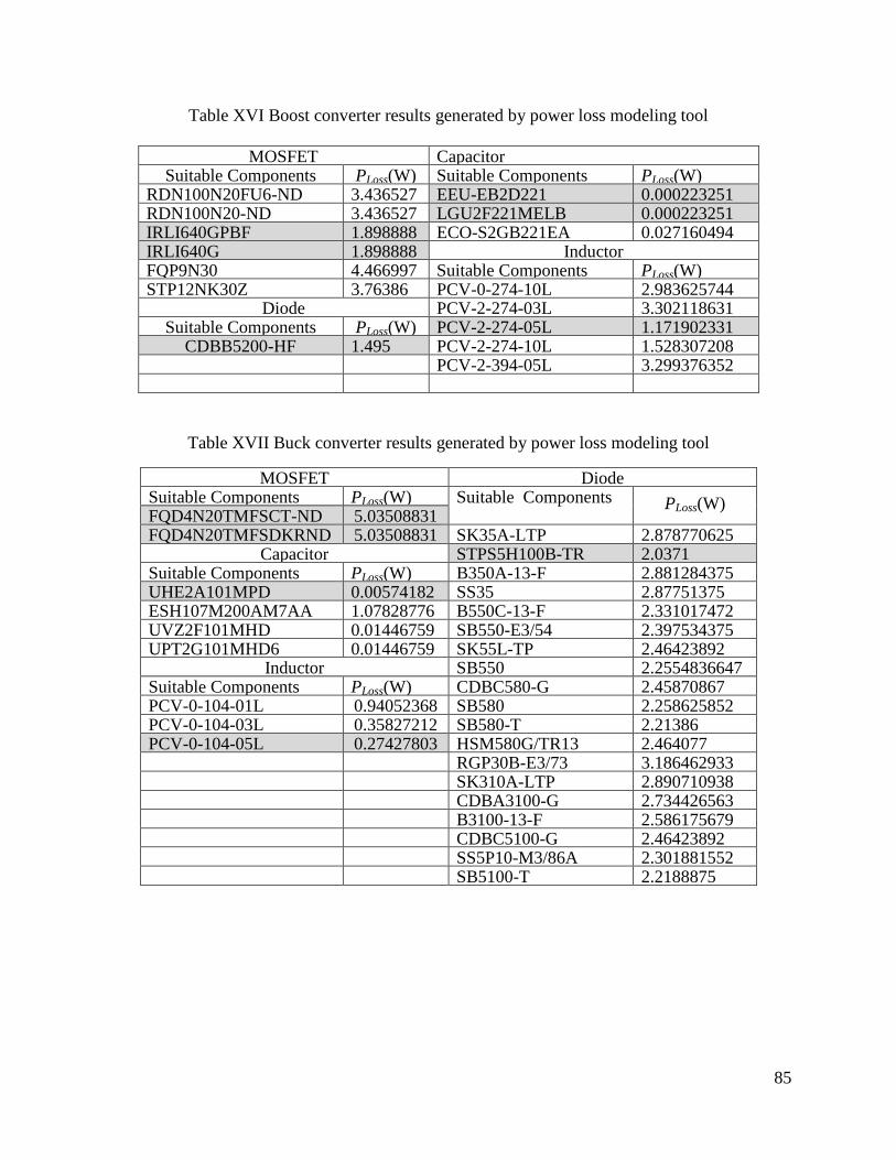
85
Table XVI Boost converter results generated by power loss modeling tool
MOSFET Capacitor Suitable Components PLoss(W) Suitable Components PLoss(W)
RDN100N20FU6-ND 3.436527
778
EEU-EB2D221 0.000223251 RDN100N20-ND 3.436527
778
LGU2F221MELB 0.000223251 IRLI640GPBF 1.898888
889
ECO-S2GB221EA 0.027160494 IRLI640G 1.898888
889
Inductor FQP9N30 4.466997
222
Suitable Components PLoss(W) STP12NK30Z
3.763864198
3.76386 PCV-0-274-10L
2.983625744 Diode PCV-2-274-03L
PCV-2-274-05L
PCV-2-274-10L
PCV-2-394-05L
3.302118631 Suitable Components PLoss(W) PCV-2-274-05L 1.171902331
CDBB5200-HF 1.495 PCV-2-274-10L 1.528307208 PCV-2-394-05L 3.299376352
Table XVII Buck converter results generated by power loss modeling tool
MOSFET Diode Suitable Components PLoss(W) Suitable Components PLoss(W) FQD4N20TMFSCT-ND 5.03508831 FQD4N20TMFSDKRND 5.03508831 SK35A-LTP 2.878770625
Capacitor STPS5H100B-TR 2.0371 Suitable Components PLoss(W) B350A-13-F 2.881284375 UHE2A101MPD 0.00574182
6
SS35 2.87751375 ESH107M200AM7AA 1.07828776 B550C-13-F 2.331017472 UVZ2F101MHD 0.01446759
3
SB550-E3/54 2.397534375 UPT2G101MHD6 0.01446759
3
SK55L-TP 2.46423892 Inductor SB550 2.2554836647
7273 Suitable Components PLoss(W) CDBC580-G 2.45870867 PCV-0-104-01L 0.94052368
3
SB580 2.258625852 PCV-0-104-03L 0.35827212 SB580-T 2.21386 PCV-0-104-05L 0.27427803
6
HSM580G/TR13 2.464077 RGP30B-E3/73 3.186462933 SK310A-LTP 2.890710938 CDBA3100-G 2.734426563 B3100-13-F 2.586175679 CDBC5100-G 2.46423892 SS5P10-M3/86A 2.301881552 SB5100-T 2.2188875

86
Table XVIII Flyback converter results generated by power loss modeling tool
MOSFET Capacitor Suitable Components PLoss(W) Suitable Components PLoss(W) ZXMN20B28KTCCT-ND 1.293020308 EEU-FC2A220 0.003203172 ZXMN20B28KTCDKRND 1.293020308 EEU-EB2D220 0.006851628
Primary winding UPJ2F220MHD1TN 0.009106776 Suitable Components PLoss(W) EKXG401ELL220MK
20S
0.01097266 Powerwerx Wire-MW-18-1 8.7940e-04 ECA-2AM470 9.72443E-05
Secondary winding EEU-ED2C470 0.000145076 Suitable Components Suitable
Components
UPB2E470MHD1TO 0.000145076 Powerwerx Wire-MW-20-1 8.7940e-04 ECO-S2GA470BA 0.014191632
Cores 380LX470M500H012 0.003591 Suitable Components PLoss(W) UHE2A101MPD 3.64846E-05 B65713 0.000263 ESH107M200AM7A
A
0.006851628 B65805 0.002582 UVZ2F101MHD 9.19296E-05 B66361 0.00216 UPT2G101MHD6 9.19296E-05 B66285 0.002582 EEU-FC2A221 0.001249668 B65814 0.001417 EEU-EB2D221 3.11699E-05 B66288 0.001759 LGU2F221MELB 3.11699E-05 B66287 0.00098 ECO-S2GB221EA 0.003792096 B66291 0.00098 ECA-2AHG471 7.77092E-06 B66387 0.000562 SLP471M200E1P3 0.006075972 B65684 0.000562 ELXM3B1VSN471M
A35S
0.006075972 Diode EET-HC2G471LA 1.46513E-05
Suitable Components PLoss(W) EKMS501VSN471M
A60S
1.93914E-05 SS15 0.115716 ECA-2AHG102 3.64846E-06 GF1A-E3/67A 0.102843 EET-UQ2D102EA 0.00129276 SS15E-TP 0.104059 350LSQ1000MNB36
X98
0.00129276 SK15-13-F 0.107342 B43508A9108M000 0.00172368 SS18-TP 0.108761 ALS30A102KF500 0.001378944 SS18 0.116216 B180-13-F 0.104988 CDBA180-G 0.11361
5.2.2 Cost Modeling in the Optimization Mode
Designers have to review vast amounts of catalog and web content in order to select low cost
components that fit their design and budget. This iterative process adds a significant burden in
terms of time and effort. Using the optimized mode the cost modeling tool, components in a
database are automatically filtered on the basis of various ratings and operating conditions, and
components with minimum cost are selected

87
5.2.2.1 Pseudo Code for Cost Modeling in the Optimization Mode
Start
Get input and output parameters;
L=((Vin×Duty×(1-Duty))/(2×fsw×Iout)); Lmax=2×L;
Read inductor.xls file and get all the database;
for i=1 to all database
if L <=inductor values in database && Lmax > inductor values in database
Extract ACR, DCR and RC values from database;
Extract unit costs and multiple unit costs data base;
end i=i+1;
end
Find minimum cost of the component for unit quantity;
Find minimum cost of the component for multiple quantities;
if minimum quantity=1;
print minimum cost of the component for unit quantity;
else if minimum quantity=1000;
print minimum cost of the component multiple quantities;
end elseif;
end if;
Calculate PACR, PDCR and PCORE as described in power loss model;
Ploss_inductor= PACR+ PDCR +PCORE ;
Print component name; Print component cost;
5.2.2.2 Flowchart for Cost Modeling in the Optimization Mode
Figure 52 shows the detailed flowchart of the optimization technique implementation for the
cost modeling tool.

88
Start
New
Component
Set converter ratings
End
Yes
Yes
No
No
Calculate inductance and
max inductance values
Check
component
availability
Check it is
within current
range?
Extract all components with
suitable ratings and their cost valuesComponent is not availble
Find minimum cost for
selected components
Find minimum cost for
1000 quantities of
selected components
Calculate power
loss of component
Print component and component
power loss
New
Component?
Figure 52 Optimization mode flowchart for the cost modeling tool

89
5.2.2.3 Results for Cost Modeling in the Optimization Mode
The cost model shown above was integrated into a user-friendly GUI developed in
MATLAB to establish a rapid-prototyping tool. The optimization mode cost model generates the
component list and lowest price of the selected components. Figures 53-55 present the boost,
buck, and flyback converter cost estimates in optimization mode. Costs of the components
selected through this mode are found to be the least values when compared with the component
list shown in Table XIX. An example of the tradeoff between minimum power loss and
minimum cost is shown in Table XIX and XX for the boost converter. If a component is selected
on the basis of minimum cost, then it may not result in a power efficient circuit. Similarly when a
component is selected only based on lowest power loss it may lead to an efficient but expensive
solution. Table XIX shows those selected components that have a higher power loss at the lowest
available cost while table XX shows the selected components with lowest power loss and highest
cost. Table XXI and XXII show the selected components for buck and flyback converters.
Figure 53 Boost converter Optimization mode cost modeling tool

90
Table XIX Boost converter results generated by optimization mode cost modeling tool with
minimum cost as the optimization objective
MOSFET
Suitable
Components
Cost($) PLoss(W)
RDN100N20FU6-
ND
2.73 3.436527778
RDN100N20-ND 2.73 3.436527778
IRLI640GPBF 2.88 1.898888889
IRLI640G 2.88 1.898888889
FQP9N30 1.18 4.466997222
STP12NK30Z 1.95 3.763864198
Diode
Suitable
Components
Cost($) PLoss(W)
CDBB5200-HF 0.21 1.495020814
Inductor
Suitable
Components
Cost($) PLoss(W)
PCV-0-274-10L
PCV-2-274-03L
PCV-2-274-05L
PCV-2-274-10L
PCV-2-394-05L
4.08 2.983625744
PCV-2-274-03L 4.15 3.302118631
PCV-2-274-05L 4.56 1.171902331
PCV-2-274-10L 7.39 1.528307208
PCV-2-394-05L 5.1 3.299376352
Capacitor
Suitable
Components
Cost($) PLoss(W)
EEU-EB2D221 2.56 0.000223251
LGU2F221MELB 7.022 0.000223251
ECO-S2GB221EA 4.68 0.027160494

91
Table XX Boost converter results generated by optimization mode cost modeling tool with
lowest power loss as the optimization objective
MOSFET
Suitable
Components
Cost($) PLoss(W)
RDN100N20FU6-
ND
2.73 3.436527778
RDN100N20-ND 2.73 3.436527778
IRLI640GPBF 2.88 1.898888889
IRLI640G 2.88 1.898888889
FQP9N30 1.18 4.466997222
STP12NK30Z 1.95 3.763864198
Diode
Suitable
Components
Cost($) PLoss(W)
CDBB5200-HF 0.21 1.495020814
Inductor
Suitable
Components
Cost($) PLoss(W)
PCV-0-274-10L
PCV-2-274-03L
PCV-2-274-05L
PCV-2-274-10L
PCV-2-394-05L
4.08 2.983625744
PCV-2-274-03L 4.15 3.302118631
PCV-2-274-05L 4.56 1.171902331
PCV-2-274-10L 7.39 1.528307208
PCV-2-394-05L 5.1 3.299376352
Capacitor
Suitable
Components
Cost($) PLoss(W)
EEU-EB2D221 2.56 0.000223251
LGU2F221MELB 7.022 0.000223251
ECO-S2GB221EA 4.68 0.027160494

92
Figure 54 Buck converter optimization mode cost modeling tool
Table XXI Buck converter results generated by optimization mode cost modeling tool
MOSFET Diode Suitable Components Cost($) Suitable Components Cost($)
FQD4N20TMFSCT-ND 0.67 SK35A-LTP 0.57 FQD4N20TMFSDKR-ND 0.67 STPS5H100B-TR 1.4
Capacitor B350A-13-F 0.46 Suitable Components Cost($) SS35 0.63
UHE2A101MPD 0.56 B550C-13-F 0.95 ESH107M200AM7AA 1.02 SB550-E3/54 0.61
UVZ2F101MHD 1.85 SK55L-TP 0.49 UPT2G101MHD6 2.68 SB550 0.56
Inductor CDBC580-G 0.74
Suitable Components Cost($) SB580 0.59
PCV-0-104-01L 1.31 SB580-T 0.43 PCV-0-104-03L 1.48 HSM580G/TR13 1.34 PCV-0-104-05L 2.37 RGP30B-E3/73 0.476
SK310A-LTP 0.57 CDBA3100-G 0.63 B3100-13-F 0.68 CDBC5100-G 0.74 SS5P10-M3/86A 0.77 SB5100-T 0.74

93
Figure 55 Flyback converter optimization mode cost modeling tool

94
Table XXII Flyback converter results generated by optimization mode cost modeling tool
MOSFET Capacitor
Suitable Components Cost($) Suitable Components Cost($)
ZXMN20B28KTCCT-
ND
0.78 EEU-FC2A220 0.502
ZXMN20B28KTCDKR
-ND
0.78 EEU-EB2D220 0.69
Primary winding UPJ2F220MHD1TN 1.32
Suitable Components Cost($) per ½ lb EKXG401ELL220MK
20S
1.72
Powerwerx Wire-MW-
18-1
26.95 ECA-2AM470 0.426
Secondary winding EEU-ED2C470 0.724
Suitable Components Cost($) per ½ lb
Components
UPB2E470MHD1TO 1.668
Powerwerx Wire-MW-
20-1
27.74 ECO-S2GA470BA 1.314
Cores 380LX470M500H012 5.41
Suitable Components Cost($) UHE2A101MPD 0.56
B65713 10.08 ESH107M200AM7AA 1.02
B65805 0.43 UVZ2F101MHD 1.85
B66361 0.51 UPT2G101MHD6 2.68
B66285 1.07 EEU-FC2A221 2.018
B65814 1.07 EEU-EB2D221 2.56
B66288 0.36 LGU2F221MELB 7.022
B66287 2.72 ECO-S2GB221EA 4.68
B66291 2.72 ECA-2AHG471 1.69
B66387 5.6 SLP471M200E1P3 3.198
B65684 3.54 ELXM3B1VSN471M
A35S
15.88
Diode EET-HC2G471LA 7.904
Suitable Components Cost($) EKMS501VSN471M
A60S
26.83333333
SS15 0.41 ECA-2AHG102 2.762
GF1A-E3/67A 0.17 EET-UQ2D102EA 5.264
SS15E-TP 0.4 350LSQ1000MNB36
X98
14.244
SK15-13-F 0.95 B43508A9108M000 20.305
SS18-TP 0.39 ALS30A102KF500 36.1
SS18 0.46
B180-13-F 0.82
CDBA180-G 0.54
Thus, the rapid prototyping tools developed here can provide two modes of operation for
designers. In this chapter these modes have been explained with the help of GUI models and the
results obtained from these models are verified experimentally and manually. The results shown
in Tables II, IV, VI and XV are obtained from component-specific mode while Tables XVI-XXII
provide results for manual mode. Results for component-specific mode operation are verified

95
with the help of experimentally implemented boost, buck and flyback converters and the results
for optimization mode are verified manually. These two modes of operation help in selecting the
components such that they are useful in maximizing the efficiency of the circuit or provide a cost
effective solution.

96
CHAPTER 6: CONCLUSION AND FUTURE WORK
Rapid prototyping tools are presented here in optimization mode and component-specific
mode. With these two modes of operation the users can estimate power loss or cost of the
components as well as that of the overall system. These two modes of operation aid in
component selection process by estimating the cost and performance of the component within
the converter system before finalizing it. The rapid prototyping tools can be useful for engineers
and designers. The power loss and cost models are found to be 92% accurate. These tools have
been verified as major time and cost saving applications and they can be easily scaled up to
include many other applications such as in inverters, motor drives, and lighting applications.
The review of existing literature was instrumental in providing insights about developing
more accurate power loss and cost models. Since most of the existing research did not consider
non-idealities and parasitic elements while calculating power loss of components. Moreover,
PCBs and gate drive losses are also not considered in the existing power loss models. The power
loss models presented here are based on non-idealities and parasitic elements including PCB and
gate drive losses to develop more accurate models. Derivation for all power loss models are
presented and discussed in detail. These models are based on converter specifications and
datasheet information so that the users can predict power losses in the circuits before finalizing
their converter design.
Cost models were derived based on an extensive survey of the commercial devices followed
by a cost surface fitting and curve fitting exercise. Component cost equations are obtained with
the help of these tools and further verified with actual cost of the components. The error
observed in this verification was less than 10%. Existing literature does not discuss the core and
magnet wire cost estimation models which are important for flyback transformers. These models

97
derived here can be helpful for designers while designing flyback transformers as well. It is
important to note that component technology and cost profiles change over time as a result of
changes in material and manufacturing techniques. The rapid prototyping tools developed in this
research intend to develop power loss and cost modeling methodologies that can evolve with
time and changes in technology.
The rapid prototyping tools are prepared as with the aim of saving time and cost. These tools
are divided into two categories to improve selection process. Optimization mode for power loss
models helps to select components based on the least power loss whereas component-specific
mode can provide power losses of each selected components. Similarly optimization mode for
cost models selects the components based on lowest costs while the component-specific mode
can provide cost estimates for a specific range of component parameters. Although the
techniques for component selection process developed here are shown to be successful, the
models presented here cannot provide power loss or cost estimates for other applications.
However, they can be easily scaled and extended for other applications based on a similar
methodology and approach. Similarly, the rapid prototyping tools are limited to power loss and
cost models, but can be extended not only for other applications but also for other models such as
reliability models.
The component-specific mode work well with power losses for basic power electronic
components, PCBs and gate drive circuits, but further work should be done to estimate power
losses within microcontroller or DSP. The cost model with component-specific mode can
estimate the ceiling prices of components, however further work is needed in order to obtain a
minimum value of ‘floor’ price of the component. In conclusion, this research provides a simple,
flexible and user-friendly way of selecting components to design systems by considering the

98
vital elements of power loss and cost in the design phase itself. These methods and models are
highly accurate and scalable considering the early stage of their application in the overall system
design process. Finally, this research will be helpful to all designers and engineers to prepare
their own rapid prototyping tools for the applications of their choice. The prepared tools can also
be useful for component distributors who can implement these tools in a web-based environment.

99
APPENDIX I COMPONENT-SPECIFIC MODE RESULTS FOR DIFFERENT DUTY RATIOS
Table A1 Boost converter component-specific mode results for different duty ratios
Parameters Duty Ratios
30% 40% 50% 60% 75%
Vin 20 20 20.1 20 20
Iin 0.45 0.6 0.88 1.35 3.50
Vout 28 33 39.8 49.3 77.4
Iout 0.3 0.34 0.42 0.52 0.85
Fsw 50KHz 50KHz 50KHz 50KHz 50KHz
D 0.3 0.4 0.5 0.6 0.75
Pin 9.00 12.00 17.69 27 70
Pout 8.4 11.22 16.72 25.63 65.79
Ploss 0.6 0.78 0.97 1.36 4.21
PCM 0.002 0.005 0.012 0.03 0.27
PSW 0.03 0.04 0.07 0.10 0.28
PGD 0.06 0.06 0.064 0.06 0.064
Ploss_Mosfet 0.10 0.11 0.14 0.19 0.61
PCD 0.32 0.4 0.44 0.55 0.89
PSWD 0.08 0.1 0.1 0.14 0.28
Ploss_Diode 0.4 0.5 0.54 0.69 1.18
PCORE 0.02 0.04 0.1 0.23 0.93
PDCR 0.01 0.02 0.05 0.11 0.74
PACR 0 0 0 0 0
Ploss_Inductor 0.03 0.06 0.15 0.34 1.67
Ploss_Capacitor 0.01 0.02 0.03 0.04 0.062
PGDRV 0 0 0 0 0
PPCB 0.02 0.03 0.06 0.1 0.67
PTotal 0.56 0.72 0.92 1.37 4.19
%Error
6.6
7.69 5.15 -0.74 0.43

100
Table A2 Buck converters component-specific mode results for different duty ratios
Parameters Duty Ratios
20% 30% 40% 50% 60%
Vin 60 60 62 61 46
Iin 0.28 0.6 1.1 1.65 1.6
Vout 12.4 18 24.6 30 27.1
Iout 1.15 1.79 2.55 3.12 2.55
Fsw 50KHz 50KHz 50KHz 50KHz 50KHz
D 0.2 0.3 0.4 0.5 0.6
Pin 16.80 36 68.20 100.65 73.60
Pout 14.03 32.22 62.73 93.6 69.11
Ploss 2.54 3.76 5.47 7.05 4.49
PCM 0.06 0.20 0.52 0.94 0.75
PSW 0.13 0.21 0.31 0.38 0.24
PG 0.04 0.04 0.04 0.04 0.03
Ploss_Mosfet 0.23 0.45 0.87 1.36 1.01
PCD 0.93 1.27 1.56 1.59 1.04
PSWD 0.06 0.09 0.12 0.15 0.13
Ploss_Diode 0.99 1.36 1.68 1.74 1.17
PCORE 0.41 0.41 0.41 0.41 0.41
PDCR 0.05 0.11 0.22 0.33 0.22
PACR 0.49 0.79 1.09 1.13 0.59
Ploss_Inductor 0.95 1.31 1.72 1.87 1.22
Ploss_Capacitor 0.20 0.32 0.44 0.45 0.24
PGDRV 0 0 0 0 0
PPCB 0.13 0.19 0.70 1.13 0.83
PTotal 2.49 3.78 5.41 6.55 4.47
%Error
1.96 -0.52 0.45 7.09 0.45

101
Table A3 Flyback converters component-specific mode results for different duty ratios
Parameters Duty Ratios
20% 30% 40% 50%
Vin 11.7 11.6 11.6 11.2
Iin 0.075 0.2 0.2 0.38
Vout 9.26 11.1 14.7 19.6
Iout 0.06 0.16 0.1 0.15
Fsw 100KHz 100KHz 100KHz 100KHz
D 0.2 0.3 0.4 0.5
Pin 0.88 2.32 2.32 4.26
Pout 0.56 1.78 1.47 2.94
Ploss 0.32 0.55 0.85 1.32
PCM 0.05 0.12 0.28 0.52
PSW 0.01 0.02 0.03 0.04
PGD 0.02 0.02 0.02 0.02
Ploss_Mosfet 0.08 0.16 0.32 0.58
PCD 0.05 0.11 0.06 0.08
PSWD 0.09 0.11 0.14 0.19
Ploss_Diode 0.14 0.22 0.20 0.27
PCORE 0.02 0.02 0.02 0.02
Ppri 0.002 0.004 0.01 0.01
Psec 0.01 0.02 0.04 0.05
Ploss_Inductor 0.03 0.05 0.07 0.09
Ploss_Capacitor 0.02 0.02 0.06 0.08
Psn 0.04 0.10 0.14 0.21
PPCB 0.004 0.01 0.02 0.04
PTotal 0.31 0.56 0.81 1.27
%Error
3.13 -1.81 4.7 3.78

102
APPENDIX II OPTIMIZATION MODE RESULTS FOR DIFFERENT DUTY RATIOS
Table A4 Boost and buck converter parameters for GUI model
Boost Converter Buck Converter
Parameters Case 1 Case 2 Case 3 Case 1 Case 2 Case 3
Vin (V) 50 40 20 50 200 200
Iin (A) 4 2.1 2 0.5 2 1.5
Vout (V) 120 80 130 25 160 120
Iout (A) 2.1 0.9 0.3 1 2.5 2.5
Duty 0.6 0.5 0.85 0.5 0.8 0.6
fsw (KHz) 100 100 50 50 50 100
Voutripple(V) 0.1 0.1 0.1 0.2 0.1 0.2
Table A5 Boost converter power loss model results for Case 1
MOSFET Diode
Suitable Components PLoss(W) Suitable Components PLoss(W)
FQP9N30 6.0472777
78
RD0504T-TL-H 3.633955
2 STP12NK30Z 4.1921913
58
BY229B-400HE3/45 5.533324
444 IRF740PBF 5.8689506
17
STTH5L04DEE-TR 3.2627
IRF740STRLPBF 5.8689506
17
Capacitor
SiHB10N40D 6.1370370
37
Suitable Components PLoss(W)
Inductor LGU2F221MELB 0.000223
251 Suitable Components PLoss(W) ECO-S2GB221EA 0.027160
4938271
605
PCV-2-274-03L 4.4202524
52
PCV-2-274-05L 1.5975424
87
PCV-2-274-10L 2.0457273
54
Table A6 Boost converter power loss model results for Case 2
MOSFET Inductor
Suitable Components PLoss(W) Suitable Components PLoss(W)
FQD7N20LTMDKR-
ND
2.4663682
77
PCV-2-394-05L 1.318871
494 BUZ73AL H-ND 1.8637325
07
JAN2N6798U-MIL 1.2855430
81
FQD7N30TMTR-ND 2.0267703
92
Capacitor
Diode
Suitable Components PLoss(W)
Suitable Components PLoss(W) EEU-ED2C470 0.000221
346 S320 1.774 UPB2E470MHD1TO 0.000221
346 PDS3200-13 1.659 ECO-S2GA470BA 0.021652
422 GI912-E3/73 2.007 380LX470M500H012 0.005478
852

103
Table A7 Boost converter power loss model results for Case 3
Table A8 Buck converter power loss model results for Case 1
MOSFET Inductor
Suitable Components PLoss(W) Suitable Components PLoss(W)
FQT7N10LTFCT-ND 0.4254166
67
PCV-2-223-05L 0.0503284
24 FQT7N10LTFDKR-ND 0.4254166
67
PCV-2-223-10L 0.0490967
FQT7N10TFTR-ND 0.3047916
67
PCH-27X-223-LT 56.996215
71 ZXMN20B28KTCCT-
ND
0.6625 RFB1010-221L 3.4780687
48 ZXMN20B28KTCDKR
-ND
0.6625 PCV-0-224-03L 0.1401287
14 Diode
Suitable Components PLoss(W)W)
SS15 0.9509380
63
Capacitor
GF1A-E3/67A 1.0959235
77
Suitable Components PLoss(W)
SS15E-TP 0.8867728
96
EEU-FC2A220 0.0743333
33 SK15-13-F 0.9124580
43
EKXG401ELL220MK
20S
0.2546333
33 SS18-TP 0.8416144
11
EEU-EB2D220 0.159
SS18 0.9512507
5
UPJ2F220MHD1TN 0.2113333
33 B180-13-F 0.9214661
68
CDBA180-G 0.9575686
32
RS1B-E3/5AT 1.1698561
44
CDBM1100-G 0.9575045
SS110-TP 0.8429902
36
SB1100 0.9568791
25
MOSFET Diode
Suitable Components PLoss(W) Suitable Components PLoss(W)
FQD7N30TMTR-ND 2.5106656
25
UVZ2F101MHD 0.00019
IRF730PBF 3.4607854
59
UPT2G101MHD6 0.00019
IRF730STRRPBF 3.4607854
59
Inductor
STP7NK40Z 3.4570348
64
Suitable Components PLoss(W)
STD9NM40N 2.7229388
07
PCV-2-564-02L 12.71139
138 STD6NK50ZT4 4.1627202
59
PCV-2-564-06L 8.046394
52 FDD6N50FTM 4.0036300
49
PCV-2-564-08L 4.245614
201 NDF05N50ZH 5.1767546
77
DO5040H-684KLB 37.92929
184 Diode
Suitable Components PLoss(W)
RGP30G-E3/73 0.6374304
62

104
Table A9 Buck converter power loss model results for Case 2
Table A10 Buck converter power loss model results for Case 3
MOSFET Diode
Suitable Components PLoss(W) Suitable Components PLoss(W)
IRF720 9.7368333
33
RGP30G-E3/73 2.2659598
72 IRF720SPBF 9.7368333
33
RD0504T-TL-H 2.0181925
IRF720STRRPBF 9.7368333
33
STTH5L04DEE-TR 1.7395036
9 IRF730PBF 5.8348333
33
Inductor
IRF730STRRPBF 5.8348333
33
Suitable Components PLoss(W)
STP7NK40Z 5.7425 PCV-0-104-01L 4.6252808
48 STD9NM40N 4.3583333
33
PCV-0-104-03L 1.7468856
92 STD6NK50ZT4 7.2584166
67
PCV-0-104-05L 1.3359644
82 FDD6N50FTM 7.2375 Capacitor
NDF05N50ZH 8.4320833
33
Suitable Components PLoss(W)
STP8N80K5 5.955 UPB2E470MHD1TO 0.021042
SPD06N80C3 5.9575 ECO-S2GA470BA 2.058333
IXTH6N80A 9.8833333
33
380LX470M500H012
380LX470M500H012
0.520833
MOSFET Diode
Suitable Components PLoss(W) Suitable Components PLoss(W)
IRF730PBF 7.0840833
33
RGP30G-E3/73 1.1569199
36 IRF730STRRPBF 7.0840833
33
RD0504T-TL-H 1.0370262
5 STP7NK40Z 7.0379166
67
STTH5L04DEE-TR 0.8737418
45 STD9NM40N 5.4708333
33
BYC5DX-500,127 1.0616713
54 STD6NK50ZT4 8.6292083
33
RGP30J-E3/73 1.0753008
11 FDD6N50FTM 8.4104166
67
CN649 0.9847395
21 NDF05N50ZH 10.466041
67
LXA03B600 1.7456863
54 STP8N80K5 6.9358333
33
BYV25D-600,118 0.9804920
45 SPD06N80C3 6.72875 LQA05TC600 1.2823453
41 IXTH6N80A 10.775 Capacitor
Inductor Suitable Components PLoss(W)
Suitable Components PLoss(W) UPT2G101MHD6 0.0133333
33 PCV-2-223-05L 0.1884615
37
PCV-2-223-10L 0.1685322
16
PCH-27X-223_LT 136.29945
72
PCV-0-224-03L 1.0476876
05

105
Table A11 Boost converter cost model results for Case 1
MOSFET Diode
Suitable Components Cost($) Suitable Components Cost($)
FQP9N30 1.18 RD0504T-TL-H 1.05
STP12NK30Z 1.95 BY229B-400HE3/45 1.03
IRF740PBF 1.63 BYC5DX-500,127 0.35
IRF740STRLPBF 1.63 BYV25D-600,118 0.848
SiHB10N40D 1.79 LQA05TC600 1.41
Inductor BY229B-600HE3/45 5.5333244
44 Suitable Components Cost($) LQA08TC600 1.93
PCV-2-274-03L 4.15 QH08TZ600 1.85
PCV-2-274-05L 4.56 MURF860G 0.99
PCV-2-274-10L 7.39 Capacitor
Suitable Components Cost($)
LGU2F221MELB 7.022
ECO-S2GB221EA 4.68
Table A12 Boost converter cost model results for Case 2
MOSFET Diode
Suitable Components Cost($) Suitable
Components
Cost($)
FQD7N20LTMDKR-
ND
0.98 GI912-E3/73 0.48
BUZ73AL H-ND 1.26 RGP30G-E3/73 0.45
JAN2N6798U-MIL 4.34 RD0504T-TL-H 1.05
RDN100N20FU6-ND 2.73 Capacitor
RDN100N20-ND 2.73 Suitable
Components
Cost($)
IRLI640GPBF 2.88 EEU-ED2C470 0.724
IRLI640G 2.88 UPB2E470MHD1T
O
1.668
FQD7N30TMTR-ND 1.04 ECO-S2GA470BA 1.314
FQP9N30 1.18 380LX470M500H01
2
5.41
STP12NK30Z 1.95 Inductor
Suitable
Components
Cost($)
PCV-2-394-05L 5.1

106
Table A13 Boost converter cost model results for Case 3
MOSFET Inductor
Suitable Components Cost($) Suitable
Components
Cost($)
FQD7N30TMTR-ND 1.04 PCV-2-564-02L 3.78
FQP9N30 1.18 PCV-2-564-06L 6.46
STP12NK30Z 1.95 PCV-2-564-08L 10.79
IRF730PBF 1.26 Capacitor
IRF730STRRPBF 1.51 Suitable
Components
Cost($)
STP7NK40Z 1.56 UVZ2F101MHD 1.85
STD9NM40N 1.67 UPT2G101MHD6 2.68
IRF740PBF 1.63
IRF740STRLPBF 1.63 Diode
SiHB10N40D 1.79 Suitable
Components
Cost($)
STD6NK50ZT4 1.18 LQA05TC600 1.41
FDD6N50FTM 1.1 RGP30G-E3/73 0.45
NDF05N50ZH 0.94 RD0504T-TL-H 1.05
TK10A50D 1.89 BYC5DX-500,127 0.35
STP11NK50ZFP 1.93 RGP30J-E3/73 0.495
IPA50R350CP 1.12 LXA03B600 0.81
FDPF12N50UT 1.73 BYV25D-600,118 0.848
Table A14 Buck converter cost model results for Case 1
MOSFET Inductor
Suitable Components Cost($) Suitable
Components
Cost($)
FQT7N10LTFCT-ND 0.54 PCV-2-223-05L 2.12
FQT7N10LTFDKR-
ND
0.54 PCV-2-223-10L 2.06
FQT7N10TFTR-ND 0.54 PCH-27X-223_LT 1.91
Diode RFB1010-221L 0.68
Suitable Components Cost($)W) PCV-0-224-03L 1.46
SS18-TP 0.39 Capacitor
SS18 0.46 Suitable
Components
Cost($)
B180-13-F 0.82 EEU-FC2A220 0.502
CDBA180-G 0.54 EKXG401ELL220M
K20S
1.72
RS1B-E3/5AT 0.178 EEU-EB2D220 0.69
CDBM1100-G 0.57 UPJ2F220MHD1TN 1.324
SS110-TP 0.39
SB1100 0.52

107
Table A15 Buck converter cost model results for case 2
MOSFET Diode
Suitable Components Cost($) Suitable Components Cost($)
IRF730PBF 1.26 RGP30G-E3/73 0.45
IRF730STRRPBF 1.51 RD0504T-TL-H 1.05
STP7NK40Z 1.56 STTH5L04DEE-TR 1.49
STD9NM40N 1.67 BYC5DX-500,127 0.35
STD6NK50ZT4 1.18 RGP30J-E3/73 0.495
FDD6N50FTM 1.1 CN649 0.448
NDF05N50ZH 0.94 LXA03B600 0.81
Inductor BYV25D-600,118 0.84
Suitable Components Cost($) LQA05TC600 1.41
PCV-2-223-05L 2.12
PCV-2-223-10L 2.06 Capacitor
PCH-27X-223_LT 1.91 Suitable Components Cost($)
PCV-0-224-03L 1.46 UPT2G101MHD6 2.68
Table A16 Buck converter cost model results for case 3
MOSFET Diode
Suitable
Components
PLoss(W) Suitable Components PLoss(W)
IRF720 3.18 RGP30G-E3/73 0.45
IRF720SPBF 1.51 RD0504T-TL-H 1.05
IRF720STRRPBF 1.51 STTH5L04DEE-TR 1.49
IRF730PBF 1.26 Inductor
IRF730STRRPBF 1.51 Suitable Components PLoss(W)
STP7NK40Z 1.56 PCV-0-104-01L 1.31
STD9NM40N 1.67 PCV-0-104-03L 1.48
STD6NK50ZT4 1.18 PCV-0-104-05L 2.37
FDD6N50FTM 1.1 Capacitor
NDF05N50ZH 0.94 Suitable Components PLoss(W)
UPB2E470MHD1TO 1.668
ECO-S2GA470BA 1.314
380LX470M500H012
380LX470M500H012
5.41

108
APPENDIX III DETAILED DERIVATIONS OF EQUATIONS
For equation (60) and (72) IDrms is obtained by taking RMS value of ID where ID is represented as
shown in Figure 4.
IDrms is represented as
2
0
1
2
DT
Drms
i iI Iout t dt
T DT
, (A1)
2 2 2
2 2
0
1 2
2 2
DT
Drms out out
i i t it iI I I dt
T DTD T
(A2)
2 2 22 2
04 3 2
DT
Drms out out out
i D i D i tI DI DI i t iDI t
(A3)
2 2 22 3 4 6
12Drms out
i D i D i DI DI
(A4)
22
12Drms out
iI D I
(A5)
Similar approach is implemented to calculate IDrms of the boost converter.
IDrms represented in (85) and Figure 14 is calculated as,
1
3Drms Lpk
DI I , (A6)
1
3
sDrms Lpk
s
D TI I
T , (A7)
but 1ON sT DT , (A8)
0.8 S out F
ON
F
T V VT
V
, (A9)

109
0.81
3
S out FinDrms
S Fsw pri m
T V VV DI
T Vf L L
, (A10)
0.26 1in out
Drms
Fsw pri m
V D VI
Vf L L
, (A11)
To calculate IDoff of the flyback transformer current (86), ILavg in (92) and (93) is calculated
with the help of (84) as,
1 22
LPKLavg
II D D , (A12)
0.8
2m pri sw
inLavg
L L f
V DI
, (A13)
0.4
m pri sw
inLavg Lpri
L L f
V DI I
, (A14)
0.4
m pri sw
inLsec
L L f
nV DI
, (A15)
0.8
2 2m pri sw m pri sw
in inDoff
L L f L L f
V D V DI
(A16)
0.9
m pri sw
inDoff
L L f
V DI
(A17)
RMS value of triangular waveform is given in Figure 14 calculated as,
1 2( )
3
S Srms pri LPK
S
D T D TI I
T
(A18)
( )3
ON OFFrms pri LPK
S
T TI I
T
(A19)

110
( )
0.8
3
Srms pri LPK
S
TI I
T
(A20)
( ) 0.26rms pri LPKI I (A21)
( ) 0.52rms pri LPKI I (A22)
(sec) 0.52rms LPKI nI (A23)
Capacitor current Icrms in (94) flyback converter
2
2(sec)
0.52
m pri sw
inCrms out
L L f
nV DI I
(A24)

111
APPENDIX IV COST MODEL EQUATIONS WITH DIFFERENT SURFACE FITS
Table A17 Surface fitting tool equations for MOSFET
Surface fitting tool results Cost Models
Lowess- quadratic SSE-51.44, R-square-0.9436
No explicit model was provided by MATLAB tool
Polynomial –x degree four
and y degree three
13
0
( , )i
i iM DS D i DS D
i
Cost V I V I
SSE-194.2, R-square-0.6717
Customize equation
2( ( ) )( , ) sin( )
IDM DS D DS DCost V I a b m V I ce
SSE-898.4, R-square-0.01473
Table A18 Surface fitting tool equations for diode
Surface fitting tool results Cost Models
Lowess- quadratic SSE: 0.07198, R-square: 0.9502
No explicit model was provided by MATLAB tool
Polynomial –x degree one
and y degree one
2
0
( , )
jj j
D B F j B F
j
Cost V I V I
SSE-0.1591, R-square-0.8899
Customize equation
2( ( ) )( , ) sin( )
IFD B F B FCost V I a b m V I ce
SSE-0.2563, R-square-0.8039
Table A19 Surface fitting tool equations for inductors
Surface fitting tool results Cost Models
Lowess- linear or quadratic Out of surface fit box
No explicit model was provided by MATLAB tool
Polynomial –x degree one and
y degree one
( , ) a+ b + cL L LCost L I L I
SSE-7693, R-square-0.3261
Customize equation
2( )( , ) sin( )
ILL L LCost L I LI e
SSE-3408, R-square-0.7014

112
Table A20 Surface fitting tool equations for capacitor
Table A21 Surface fitting tool equations for Cores
Surface fitting tool results Cost Models
Lowess- linear SSE: 1.196 R-square: 0.9882
No explicit model was provided by MATLAB tool
Polynomial –x degree two
and y degree two
4( , )
0
m mm
Cost A f A fCo L sw m L sw
m
SSE: 6.448 R-square: 0.9365
Customize equation
2( ( ) )( , ) sin( )
fswCost A f a b m A f ceCo L sw L sw
SSE: 74.43 R-square: 0.2669
Table A22 Curve fitting tool equations for Magnet wire
Curve fitting tool results Cost Models
Linear polynomial 1
0
(G)
w q
q
Cost G
Quadratic polynomial
2
0
(G)
w q
q
Cost G
Cubic polynomial
3
0
(G)
w q
q
Cost G
Polynomial 5th
degree
6
0
(G)
w q
q
Cost G
Surface fitting tool results Cost Models
Lowess- linear SSE: 139.8, R-square: 0.9091
No explicit model was provided by MATLAB tool
Polynomial –x degree two
and y degree three
8
0
( , )z
zzC C z C
z
Cost C V C V
SSE: 265.5, R-square: 0.8274
Customize equation
2( ( ) )( , ) sin( )
VCC C CCost C V a b m CV ce
SSE: 1245, R-square: 0.19

113
REFERENCES
[1] S.M.Cuk, R.D. Middlebrook, “DC-DC switching converters,” U.S. Patent 4 184 197A, Jan
15, 1980.
[2] E. Biagi, G. Pasetti, F. Tinfena, ; R. Serventi, L. Fanucci, “A High Voltage High Power high
frequency Boost/Flyback DC-DC converter for automotive applications,” in Proc. IEEE
Power Electronics, Electrical Drives, Automation and Motion conference, 2012, pp. 1166 –
1171.
[3] N.G. Ziesse, “High frequency DC-DC converter,” U.S. Patent 4 449 174A, May 15, 1984.
[4] Gu, Bin, Lin, Chien-Yu Chen, Bai Feng,Jason Dominic, Cong Zheng, Jih-Sheng Lai, “A high
efficiency hybrid resonant PWM zero-voltage-switching full-bridge DC-DC converter for
electric vehicle battery chargers ,” in Proc. IEEE Applied Power Electronics Conference and
Exposition,2013, pp. 23 – 30.
[5] M.C.W. Lindmark, “ Switched mode power supply,” U.S. Patent 4 097 773A, June 27, 1978.
[6] Dan Dai, Jing Liu, “Design of a practical human-powered contactless charger for cellphone,”
IEEE Transactions on Consumer Electronics, vol. 59, pp. 476 – 482, August 2013.
[7] W.G. Borland, “ Resonant switching converter,” U.S. Patent 4 945 466A, May 15, 1984.
[8] Ying-Chun Chuang, Yu-Lung Ke ; Hung-Shiang Chuang ; Yung-Shan Wang, “A novel
single-switch resonant power converter for renewable energy generation applications,” in
Proc. IEEE Industrial & Commercial Power Systems Technical Conference, 2013, pp.1-9.
[9] H. Wang, P. Zanchetta, J. Clare, C. Ji, “Modelling and control of a zero current switching
high-voltage resonant converter power supply for radio frequency sources,” IEEE
Transactions on Power Electronics, vol.5, pp. 401 – 409, April 2012.
[10] Jinjun Liu, Weiyun Chen, Jindong Zhang, Dehong Xu , F.C.Lee, “Evaluation of power
losses in different CCM mode single-phase boost FC converters via a simulation tool,” in
Proc. IEEE Industry Applications Conference, 2001, pp. 2455 - 2459.
[11] J.P.M.Figueiredo, F.L.Tofoli, R.L.Alves, “Comparison of non-isolated DC-DC converters
from the efficiency point of view,” in Proc. IEEE Power Electronics Conference, 2011, pp.
14-19.
[12] N. Yamashita, N. Murakami, T. Yachi, “Conduction power loss in MOSFET synchronous
rectifier with parallel-connected Schottky barrier diode,” IEEE Transactions on Power
Electronics, vol.13, pp. 667 - 673, Jul 1998.
[13] Jiaxin Chen, Ge Chen, Youguang Guo, Jianguo Zhu “Comprehensive analysis of power loss
in the output diode of flyback switching converter operating in DCM and CCM,” in Proc.
IEEE Electrical Machines and Systems, 2008, pp. 1865 – 1870.
[14] Yang Chen, P. Asadi, P. Parto, “Comparative analysis of power stage losses for
synchronous Buck converter in Diode Emulation mode vs. Continuous Conduction Mode at
light load condition,” in Proc. IEEE Applied Power Electronics Conference and Exposition,
2010, pp. 1578 – 1583.
[15] Jinjun Liu, T.G. Wilson, R.C. Wong,R. Wunderlich, F.C. Lee, “A method for inductor core
loss estimation in power factor correction applications,” in Proc. IEEE Applied Power
Electronics Conference and Exposition, 2002, pp. 439 - 445.
[16] H.Y. Chung, M.H. Pong, “Effect of switching frequency and number of winding layers on
copper loss of an inductor,” in Proc. IEEE Power Electronics and Motion Control
Conference, 2000, pp. 1312 – 1317.

114
[17] A. Braham, A. Lahyani, P.Venet, N. Rejeb, “Recent Developments in Fault Detection and
Power Loss Estimation of Electrolytic Capacitors,” IEEE Transactions on Power
Electronics, vol.25, pp. 33 - 43, Jan. 2010.
[18] I.Lope, C.Carretero, J.Acero, J.M.Burdio, R.Alonso, “Practical issues when calculating AC
losses for magnetic devices in PCB implementations,” in Proc. IEEE Applied Power
Electronics Conference and Exposition, 2012, pp. 1017 - 1022.
[19] P. Pathmanathan, C.M. Jones, S.G. Pytel, D.L. Edgar, P.G. Huray, “Power loss due to
periodic structures in high-speed packages and Printed Circuit Boards,” in Proc. IEEE
Microelectronics and Packaging Conference, 2011, pp. 1 - 8.
[20] Ren-Huei Tzeng, Chern-Lin Chen, “A Low-Consumption Regulated Gate Driver for Power
MOSFET,” IEEE Transactions on Power Electronics, vol.24, pp. 532 - 539, Feb. 2009.
[21] Zhiliang Zhang, W. Eberle, Zhihua Yang ; Yan-Fei Liu, P.C. Sen, “Optimal Design of
Current Source Gate Driver for a Buck Voltage Regulator Based on a New Analytical Loss
Model,” in Proc. IEEE Power Electronics Specialists Conference, 2007, pp. 1 - 8.
[22] M.M. Jovanovic, “A technique for reducing rectifier reverse-recovery-related losses in high-
power boost converters,” IEEE Transactions on Power Electronics, vol.13, pp. 932 - 941,
Sep. 1998.
[23] Jun Wang, Jun Li, Xiaohu Zhou, Tiefu Zhao, A.Q. Huang, R. Callanan, F. Husna, A.
Agarwal, “10 kV SiC MOSFET Based Boost Converter,” in Proc. IEEE Industry
Applications Society Annual Meeting, 2008, pp.1-6.
[24] Z.Ivanovic, B.Blanusa, M.Knezic, “Power loss model for efficiency improvement of boost
converter,” in Proc. IEEE Information, Communication and Automation Technologies, 2011,
pp. 1-6.
[25] Weiping Zhang, Yuanchao Liu, Zhi Li, Xiaoqiang Zhang, “The dynamic Power Loss
analysis in Buck Converter,” in Proc. IEEE Power Electronics and Motion Control
Conference, 2009, pp. 362 - 367.
[26] T.Lopez, R.Elferich, “Method for the Analysis of Power MOSFET Losses in a
Synchronous Buck Converter,” in Proc. IEEE Power Electronics and Motion Control
Conference, 2006, pp. 44-49.
[27] Jong-Hyun Kim, Myung hyo Ryu, Byung Duk Min, Eui Ho Song, “A Method to Reduce
Power Consumption of Active-Clamped Flyback Converter at No-Load Condition,” in Proc.
IEEE Industrial Electronics, 2006, pp. 2811 – 2814.
[28] D. Murthy-Bellur, M.K. Kazimierczuk, “Winding losses caused by harmonics in high-
frequency flyback transformers for pulse-width modulated DC-DC converters in
discontinuous conduction mode,” IEEE Transactions on Power Electronics, vol.3, pp. 804 -
817, Sep. 2010.
[29] A. Causo, A. Salati, E. Lorenzani, F. Immovilli, C. Bianchini, “Power losses analysis in
interleaved flyback based PV grid connected micro-inverters,” in Proc. IEEE Industrial
Electronics, 2013, pp. 1833 - 1838.
[30] P.Bartal, I.Nagy, “On-line efficiency estimation for DC-DC converter cluster by dedicated
software,” in Proc. Energy Conference and Exhibition, 2012, pp. 800-805.
[31] Ying-Win Bai and Wei-Chih Kuo, “Design and implementation of an automatic
measurement system for DC-DC converter efficiency on a motherboard,” in Proc. IEEE
Industrial Electronics Society Conference, 2010, pp. 1323 –1328.

115
[32] K. Viswanathan, R. Oruganti, “Evaluation of Power Losses in a Boost PFC Unit by
Temperature Measurements,” IEEE Transactions on Industry Applications, vol.43, pp. 1320
- 1328, Sept.-Oct. 2007.
[33] A. Shahin, A. Payman, J. Martin, S. Pierfederici, F. Meibody-Tabar,“Approximate Novel
Loss Formulae Estimation for Optimization of Power Controller of DC-DC Converter,” in
Proc. IEEE Industrial Electronics Society,2010, pp. 373 – 378.
[34] Pill-Soo Kim, Yong Kim, “A future cost trends of magnetizer systems in Korea,” in Proc.
IEEE Industrial Electronics, Control, and Instrumentation, 1996 , pp. 991 – 996.
[35] A.M. Roldan, A. Barrado, J. Pleite, J. Vazquez,E. Olias, “Size and cost reduction of the
energy-storage capacitors,” in Proc. IEEE Applied Power Electronics Conference and
Exposition, 2004, pp. 723 – 729.
[36] Pill-Soo Kim, Yong Kim, “Part I-circuit, thermal and cost modeling of impulse magnetizer,”
in Proc. IEEE Power Electronics and Drive Systems, 1999, pp. 371 – 376.
[37] Bruno Burger, Dirk Kranzer, Olivier Stalter, “Cost Reduction of PV-Inverters with SiC-
DMOSFETs,” in Proc. IEEE Integrated Power Systems, 2008, pp. 1 – 5.
[38] R. Burkart, J.W.. Kolar, “Component cost models for multi-objective optimizations of
switched-mode power converters,” in Proc. IEEE Energy Conversion Congress and
Exposition, 2013, pp. 2139 – 2146.
[39] Xiangyu Dong, Jishen Zhao, Yuan Xie, “Fabrication Cost Analysis and Cost-Aware Design
Space Exploration for 3-D ICs,” IEEE Computer-Aided Design of Integrated Circuits and
Systems, vol.29, pp. 1959 - 1972, Dec. 2010.
[40] A.K. Coskun, A.B. Kahng, T.S. Rosing, “Temperature- and Cost-Aware Design of 3D
Multiprocessor Architectures,” in Proc. IEEE Digital System Design, Architectures, Methods
and Tools, 2009, pp. 183 – 190.
[41] Pill-Soo Kim, “Cost modeling of battery electric vehicle and hybrid electric vehicle based
on major parts cost,” in Proc. IEEE Power Electronics and Drive Systems, 2003, pp. 1295 –
1300.
[42] P. Manimekalai, R. Harikumar, “Design, cost estimation and simulation of a standalone PV
power generation system using interleaved converter,” in Proc. IEEE Emerging Trends in
Science, Engineering and Technology , 2012, pp. 416 – 421.
[43] K. Kim, S. Lertburapa, C. Xu, and P. Krein, “Efficiency and Cost Trade- Offs for Designing
Module Integrated Converter Photovoltaic Systems,” in Proc. IEEE Power and Energy
Conference at Illinois, 2012, pp. 1–7, 2012.
[44] B. Azzopardi, J. Mutale, D. Kirschen, “Cost boundaries for future PV solar cell modules,”
in Proc. IEEE Sustainable Energy Technologies, 2008, pp. 589 – 594.
[45] P.I. Muoka, M.E. Haque,M. Negnetvitsky, “A new tool for design optimization and cost
estimation of stand-alone photovoltaic power plants,” in Proc. IEEE Power and Energy
Society General Meeting, 2011, pp. 1 – 7.
[46] Tian Weidong, “The principle of minimum production cost model for multiple area
interconnected power systems,” in Proc. IEEE Computer, Communication, Control and
Power Engineering., 1993, pp. 339 – 343.
[47] Weiwei Pan, Guowei Wu, Hui Zhou, Chong Wang, Yunhe Hou, “Risk-based life cycle cost
analysis method for transmission systems,” in Proc. IEEE Innovative Smart Grid
Technologies, 2012, pp. 1 – 5.

116
[48] Xu Xinsheng, Fang Shuiliang, Gu Xinjian, “A model for manufacturing cost estimation
based on machining feature,” in Proc. IEEE Technology and Innovation Conference, 2006,
pp. 273 – 278.
[49] K. Ma, F. Blaabjerg, “Reliability-cost models for the power switching devices of wind
power converters,” in Proc. IEEE Power Electronics for Distributed Generation Systems,
2012, pp. 820 – 827.
[50] G.A.Klutke, P.C. Kiessler, M.A.Wortman, “A critical look at the bathtub curve”, in Proc.
IEEE transaction on Reliability, vol. 52, pp. 125 – 129, Mar 2003.
[51] F. Jensen, “Component failures based on flaw distributions,” in Proc Reliability and
Maintainability Symposium, 1989, pp. 91 – 95.
[52] J. Fussel, E. Aber, and R. Rahl, “On the quantitative analysis of priorty- and failure logic,”
IEEE Transactions on Reliability, vol. 31, pp. 219–254, June 1982.
[53] Military handbook; Reliability prediction of Electronic equipments (MIL-HDBK-217),Jan
1991.
[54] K. Shenai, “Power MOSFET screening to improve field-reliability of power supplies,” in
Proc. IEEE Energytech, 2013, pp. 1 – 3.
[55] V. Banu, X. Jorda, J. Montserrat, P. Godignon, J. Millan, Pierre Brosselard, “Accelerated
test for reliability analysis of SiC diodes,” Power Semiconductor Devices & IC's, 2009, pp
267-270.
[56] E. A. Herr, A. Poe, A. Fox, “Reliability Evaluation and Prediction for Discrete
Semiconductors,” in Proc. IEEE transaction on Reliability, vol. 29, pp. 208 - 216, Aug 1980.
[57] C.Rodriguez, G. Amaratunga, “Long-Lifetime Power Inverter for Photovoltaic AC
Modules”, IEEE transaction on industrial electronics, 2008 pp. 2593 – 2601.
[58] S. V. Dhople, A. Davoudi, P. L. Chapman and A. D. Domínguez- García, “Reliability
Assessment of Fault-Tolerant DC-DC Converters for Photovoltaic Applications,” in Proc.
IEEE Energy Conversion Congress and Exposition, 2009, pp. 2271 – 2276.
[59] T. Kobayashi, H. Ariyoshi, A. Masuda, “Reliability Evaluation and Failure Analysis for
Multilayer Ceramic Chip Capacitors,” in Proc. IEEE transaction on Reliability, vol. 1, pp.
316 - 324, Sep 1978.
[60] A. Cavallini, I. Ghinello, G. Maszanti, G.C. Montanari, “Accelerated capacitor degradation
due to nonsinusoidal voltage supply and reliability of insulation systems,”in Proc. IEEE
Harmonics and Quality of Power Proceedings, 1998, pp.720-726.
[61] Juha-Veikko Voutilainen, Tuomas Happonen, Juha Hakkinen, “Reliability of silkscreen
printed planar capacitors and inductors under accelerated thermal cycling and humidity bias
life testing,” in Proc. IEEE Electronic System-Integration Technology Conference, 2012
pp.1-6.
[62] Dan Zhou, Chengrong Li, Zhongdong Wang, “Power transformer lifetime modeling,” in
Proc. IEEE Prognostics and System Health Management, 2012, pp.1-7.
[63] Na Liu, Wensheng Gao, Kexiong Tan, Liufang Wang, Guodong Liang, Wei Li , “Decision
on Maintenance Period for Power Transformer based on Monte Carlo Simulation of
Reliability,” in Proc. IEEE Properties and Applications of Dielectric Materials, 2003. pp.
479 - 482.
[64] M.K. Alam, F.H. Khan, “Reliability analysis and performance degradation of a Boost
converter,” in Proc. IEEE Energy Conversion Congress and Exposition, 2013 pp. 5592 -
5597.

117
[65] S. V. Dhople, A. Davoudi, P. L. Chapman and A. D. Domínguez- García, “A Unified
Approach to Reliability Assessment of Multiphase DC–DC Converters in Photovoltaic
Energy Conversion Systems,” IEEE Transactions on Power Electronics, vol. 27, pp. 739 -
751, Feb 2012.
[66] R.D. Kulkarni, V. Agarwal, “Reliability analysis of a modern power supply under nuclear
radiation effects,” in Proc. IEEE Power Electronics and Drive Systems, 2003, pp. 71 – 76.
[67] Boyi Yang, Jiann-Shiun Yuan, Z. Shen, “Reliability and failure mechanisms of lateral
MOSFETs in synchronous DC-DC buck converter,” in Proc. IEEE Physical and Failure
Analysis of Integrated Circuits, 2009, pp. 1946-1542.
[68] A. Rahnamaee, J. Milimonfared, K. Malekian, M. Abroushan, “Reliability consideration for
a high power zero-voltage-switching flyback power supply,” in Proc. IEEE Power
Electronics and Motion Control Conference, 2008, pp. 365 - 371.
[69] Jiaxin Chen, Youguang Guo, Jianguo Zhu, Jianxun Jin, “Heavy Load Simulation Model of
Flyback Switching DC-DC Converters and its Application for Reliability Improvement,” in
Proc. IEEE Industry Applications Conference, 2007, pp. 2295 - 2302.
[70] H. Wang, M. Liserre, and F. Blaabjerg, “Toward reliable power electronics: challenges,
design tools, and opportunities," IEEE Industrial Electronics Magazine, vol. 7, no. 2, pp. 17-
26, Jun. 2013.
[71] Military handbook; Reliability prediction of Electronic equipment (MIL-HDBK-338B), Oct.
1998.
[72] A. Ranjbar, M. Kiani,B. Fahimi, “Dynamic Markov Model for Reliability Evaluation of
Power Electronic Systems”, in Proc. Power Engineering, Energy and Electrical
Drives,2011,pp.1-6.
[73] A. Aal, T. Polte, “On component reliability and system reliability for automotive
applications”, in Proc. Integrated Reliability Workshop Final Report, 2012, pp. 168-170.
[74] Qingyu Yang, Yong Chen, “Monte Carlo Methods for Reliability Evaluation of Linear
Sensor Systems,” IEEE transaction on Reliability, vol. 60, pp. 305-314, Mar 2011.
[75] S M. Molhanec, “Model based FMEA method for solar modules,” in Proc. Electronics
Technology conference 2013, pp. 183 – 188.
[76] A.M. Bazzi, Xiangyu Ding ; A. Dominguez-Garcia, P.T. Krein, “Circuit-based induction
motor drive reliability under different control schemes and safe-mode operation’, in Proc.
Applied Power Electronics Conference and Exposition 2011, pp. 653 – 660.
[77] J. Mora-Fl rez, J. Bedoya-Hernandez, S. Perez-Londono,“ Fault tree based methodology to
evaluate the reliability of converter transformers,” ,” in Proc. Transmission and Distribution
Conference and Exposition, 2008, pp. 1-7.
[78] B. Edson, Xijin Tian, “A prediction based design-for-reliability tool,” in Proc. Reliability
and Maintainability Annual Symposium, 2004, pp. 412-417.
[79] P.T.Krein “Elements of Power Electronic,” 2nd edition, Oxford University –Press, Inc. New
York, 1997.
[80] Shuai Shao, Xinke Wu, Min Chen,F. Peng, “Design considerations of a self-biased current
driven SR in DCM flyback DC-DC converter,” in Proc. IEEE Energy Conversion Congress
and Exposition, 2010, pp. 242 – 248.
[81] Jingdong Chen, “Need to estimate buck converter efficiency in portable apps,” eetimes-
India, Jan. 2008.

118
[82] A.M.Bazzi, P.T.Krein, J.W.Kimball, and K.Kepley, "IGBT and Diode Loss Estimation
under Hysteresis Switching," IEEE Transactions on Power Electronics, vol. 27, pp. 1044-
1048, Mar 2012.
[83] R.W.Erickson, “Fundamentals of Power Electronics,” 2nd
edition, Kluwer Academic
Publishers, 2001.
[84] Gary L. Johnson, “Solid State Tesla Coil,” Chapter 3, Dec 2001. [85] X.Zhang, X.Ruan, H.Kim, and C.K.Tse, “Adaptive Active Capacitor Converter for
Improving Stability of Cascaded DC Power Supply System,” IEEE Transactions on Power
Electronics, vol.28, pp. 1807-1816, Apr 2012.
[86] A.Haider, P.Variyam, A.Chatterjee, J.Ridley, “Measuring stray capacitance on tester
hardware,” in Proc. IEEE VLSI test symposium, 2002, pp. 351-356.
[87] Yang Chen, Guozhu Chen, K.Smedley, “Analysis and measurement of small inductance of
loops and vias on printed circuit board,” in Proc. IEEE Industrial Electronics Society, 2003,
pp. 1661 – 1666.
[88] H.Zumbahlenas ,“ Linear Circuit design handbook,”2nd
Edition ,Elsevier Publication,
pp821-895, 2008.
[89] A.A.Fomani, J.C.W.Ng, A.Shorten,“ An integrated segmented gate driver with adjustable
driving capability,” in Proc. IEEE Energy Conversion Congress and Exposition, 2010, pp.
2430-2433.
[90] Hamilton Confortin Sartori, Hélio Leães Hey, José Renes Pinheiro, “An optimum design of
PFC Boost Converters,” IEEE Transactions on Power Electronics, vol.13, pp. 1-8, Sept
2009.
[91] M.H.Rashid, “Power Electronics handbook-Devices, circuits and applications” 2nd Edition,
Academic press, 2007.
[92] N.Coruh, S.Urgun, T.Erfidan, “Design and implementation of flyback converter,” in Proc.
IEEE Industrial Electronics and Applications, 2010, pp. 1189 - 1193.
[93] Jian Sun, D.M.Mitchell, M.F.Greuel, P.T.Krein, R.M.Bass, “Averaged modeling of PWM
converters operating in discontinuous Conduction mode,” IEEE Transactions on Power
Electronics,vol. 16, pp. 482-492,Jul 2001.
[94] Liang Cheng ,Ye Yunyue, Zhuo Zheng, “Design of Improved Single Phase Flyback
Switching Power for PMSM Drive System,” in Proc. IEEE International conference on
Artificial Intelligence, Management Science and Electronic Commerce, 2011, pp.3898-3901.
[95] B.M.Hasaneen, A.A.E. Mohammed, “Design and simulation of DC-DC boost converter,” in
Proc. IEEE Power System Conference, 2008, pp. 335 – 340.
[96] M. El-Zanaty, M. Orabi, M.Z. El-Sadek, “Review of synchronous buck converter design
optimization,” in Proc. IEEE Power System Conference, 2008, pp. 588 – 592.
[97] T.R. Salvatierra, M.K. Kazimierczuk, “Inductor design for PWM buck converter operated as
dynamic supply or amplitude modulator for RF transmitters,” in Proc. International Midwest
Symposium on Circuits and Systems,2013, pp.37 – 40.