rapid fpga modem design techniques for sdrs using altera
TRANSCRIPT
Copyright © 2004 General Dynamics. All rights reserved.
Rapid FPGA Modem Design Techniques For SDRs Using Altera DSP Builder
Steven W. Cox Joel A. Seely General Dynamics C4 Systems Altera Corporation 8201 E. McDowell Road, MDR3125 101 Innovation Dr Scottsdale, Arizona 85257 San Jose, CA 95134 (480) 441-1736 (408) 544-8122 [email protected] [email protected]
ABSTRACT FPGA modem design techniques using Altera® DSP Builder are presented for waveforms on software-defined radios (SDRs). The benefits of using these techniquies will be highlighted. This paper assumes that FPGAs will be the target processor for most modem real-time signal processing of waveforms. The techniques presented in this paper are the result of internal research and development for a general dynamics engineering-sponsored project (ESP). In this paper, we show how the typical FPGA-based waveform design flow can be streamlined to yield maximum efficiency. Time savings in the form of development, debug, and testing will be shown in addition to a reduction in engineering resources needed to accomplish a given cycle time. The streamlined approach includes: architecture definition, subsystem design, simulation, subsystem integration, FPGA code generation, and design verification. The design flow has major advantages compared to traditional waveform development processes and provides a common environment for multi-disciplined personnel to work and communicate effectively. Some areas of tool enhancement are identified to serve as a guide for future revisions and to encourage feedback of ideas for overall design flow maturity.
1. INTRODUCTION
Software-defined radios (SDRs) are becoming ubiquitous as more systems require interoperability across multiple standards. Part of this trend is due to the heavy reliance on configurable hardware (e.g., FPGAs) used to implement the waveforms. To quickly develop these waveforms, some of which are extremely complex, tools with a higher
level of abstraction are required. Altera’s DSP Builder provides an integrated environment that can be used to develop hardware implementations of waveforms. This method streamlines the FPGA design flow using: Mathwork’s Simulink capabilities, a fixed point blockset with Altera FPGA objects, and interfaces to third-party tools to generate a synthesizable FPGA hardware description language (HDL). DSP Builder allows multi-disciplined users to work at higher levels of abstraction in a common workspace. All aspects of waveform development, including design, simulation, and verification, can be addressed at the Simulink level prior to hardware implementation.
2. TRADITIONAL FPGA WAVEFORM DESIGN METHOD
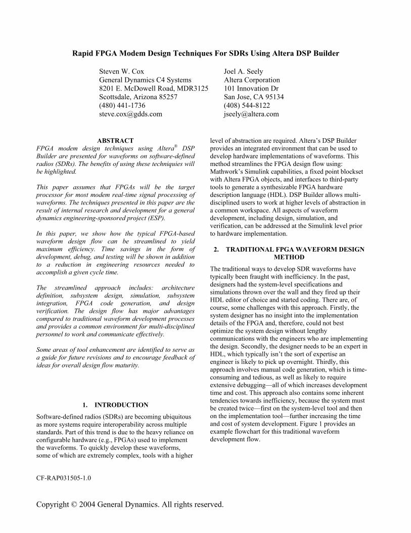
The traditional ways to develop SDR waveforms have typically been fraught with inefficiency. In the past, designers had the system-level specifications and simulations thrown over the wall and they fired up their HDL editor of choice and started coding. There are, of course, some challenges with this approach. Firstly, the system designer has no insight into the implementation details of the FPGA and, therefore, could not best optimize the system design without lengthy communications with the engineers who are implementing the design. Secondly, the designer needs to be an expert in HDL, which typically isn’t the sort of expertise an engineer is likely to pick up overnight. Thirdly, this approach involves manual code generation, which is time-consuming and tedious, as well as likely to require extensive debugging—all of which increases development time and cost. This approach also contains some inherent tendencies towards inefficiency, because the system must be created twice—first on the system-level tool and then on the implementation tool—further increasing the time and cost of system development. Figure 1 provides an example flowchart for this traditional waveform development flow.
CF-RAP031505-1.0
Copyright © 2004 General Dynamics. All rights reserved.
Figure 1: Traditional Waveform Design Flow
3. ANOTHER TOOL, A NEW APPROACH
Tools such as Altera’s DSP Builder have been developed to address the issues found when performing complex
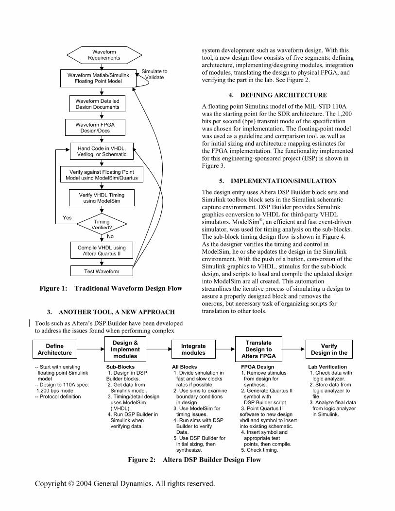
system development such as waveform design. With this tool, a new design flow consists of five segments: defining architecture, implementing/designing modules, integration of modules, translating the design to physical FPGA, and verifying the part in the lab. See Figure 2.
4. DEFINING ARCHITECTURE
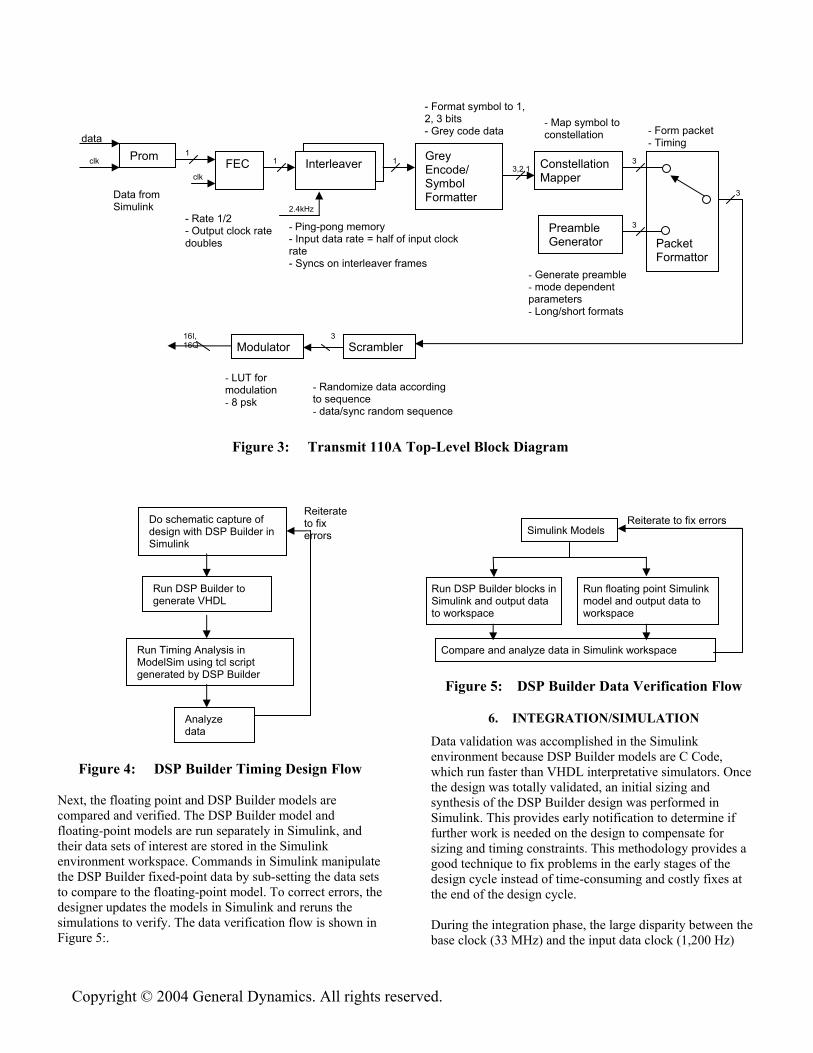
A floating point Simulink model of the MIL-STD 110A was the starting point for the SDR architecture. The 1,200 bits per second (bps) transmit mode of the specification was chosen for implementation. The floating-point model was used as a guideline and comparison tool, as well as for initial sizing and architecture mapping estimates for the FPGA implementation. The functionality implemented for this engineering-sponsored project (ESP) is shown in Figure 3.
5. IMPLEMENTATION/SIMULATION
The design entry uses Altera DSP Builder block sets and Simulink toolbox block sets in the Simulink schematic capture environment. DSP Builder provides Simulink graphics conversion to VHDL for third-party VHDL simulators. ModelSim®, an efficient and fast event-driven simulator, was used for timing analysis on the sub-blocks. The sub-block timing design flow is shown in Figure 4. As the designer verifies the timing and control in ModelSim, he or she updates the design in the Simulink environment. With the push of a button, conversion of the Simulink graphics to VHDL, stimulus for the sub-block design, and scripts to load and compile the updated design into ModelSim are all created. This automation streamlines the iterative process of simulating a design to assure a properly designed block and removes the onerous, but necessary task of organizing scripts for translation to other tools.
Figure 2: Altera DSP Builder Design Flow
-- Start with existing floating point Simulink model -- Design to 110A spec: 1,200 bps mode -- Protocol definition
Define Architecture
Design & Implement modules
Integrate modules
Translate Design to
Altera FPGAVerify
Design in the
Sub-Blocks 1. Design in DSP Builder blocks. 2. Get data from Simulink model. 3. Timing/detail design uses ModelSim (.VHDL). 4. Run DSP Builder in Simulink when verifying data.
FPGA Design 1. Remove stimulus from design for synthesis. 2. Generate Quartus II symbol with DSP Builder script. 3. Point Quartus II software to new design vhdl and symbol to insert into existing schematic. 4. Insert symbol and appropriate test points, then compile. 5. Check timing.
All Blocks 1. Divide simulation in fast and slow clocks rates if possible. 2. Use sims to examine boundary conditions in design. 3. Use ModelSim for timing issues. 4. Run sims with DSP Builder to verify Data. 5. Use DSP Builder for initial sizing, then synthesize.
Lab Verification 1. Check data with logic analyzer. 2. Store data from logic analyzer to file. 3. Analyze final data from logic analyzer in Simulink.
Waveform Matlab/Simulink Floating Point Model
Timing Verified?
Waveform Requirements
Waveform Detailed Design Documents
Simulate to Validate
Verify against Floating Point Model using ModelSim/Quartus
Verify VHDL Timing using ModelSim
Compile VHDL using Altera Quartus II
Test Waveform
Waveform FPGA Design/Docs
Hand Code in VHDL, Verilog, or Schematic
No
Yes
Copyright © 2004 General Dynamics. All rights reserved.
Figure 3: Transmit 110A Top-Level Block Diagram
Figure 4: DSP Builder Timing Design Flow
Next, the floating point and DSP Builder models are compared and verified. The DSP Builder model and floating-point models are run separately in Simulink, and their data sets of interest are stored in the Simulink environment workspace. Commands in Simulink manipulate the DSP Builder fixed-point data by sub-setting the data sets to compare to the floating-point model. To correct errors, the designer updates the models in Simulink and reruns the simulations to verify. The data verification flow is shown in Figure 5:.
Figure 5: DSP Builder Data Verification Flow
6. INTEGRATION/SIMULATION
Data validation was accomplished in the Simulink environment because DSP Builder models are C Code, which run faster than VHDL interpretative simulators. Once the design was totally validated, an initial sizing and synthesis of the DSP Builder design was performed in Simulink. This provides early notification to determine if further work is needed on the design to compensate for sizing and timing constraints. This methodology provides a good technique to fix problems in the early stages of the design cycle instead of time-consuming and costly fixes at the end of the design cycle. During the integration phase, the large disparity between the base clock (33 MHz) and the input data clock (1,200 Hz)
Do schematic capture of design with DSP Builder in Simulink
Run DSP Builder to generate VHDL
Run Timing Analysis in ModelSim using tcl script generated by DSP Builder
Analyze data
Reiterate to fix errors Simulink Models
Run DSP Builder blocks in Simulink and output data to workspace
Compare and analyze data in Simulink workspace
Reiterate to fix errors
Run floating point Simulink model and output data to workspace
- Format symbol to 1, 2, 3 bits - Grey code data
Prom data
FEC
1 1
clk
Interleaver
2.4kHz
13,2,1
Grey Encode/ Symbol Formatter
Constellation Mapper
Preamble Generator
Scrambler Modulator 16I, 16Q
3
3
3
3
Packet Formattor
Data from Simulink
- Rate 1/2 - Output clock rate doubles
- Ping-pong memory - Input data rate = half of input clock rate - Syncs on interleaver frames
- Map symbol to constellation
- Generate preamble - mode dependent parameters - Long/short formats
- Form packet - Timing
- Randomize data according to sequence - data/sync random sequence
- LUT for modulation - 8 psk
clk
Copyright © 2004 General Dynamics. All rights reserved.
was noted., which could cause the Simulink simulations to take a long time. This problem can be alleviated, however, by reducing the input data clock to be represented by 0.66 MHz instead of the full 1,200 Hz equivalent. To analyze boundary conditions between frames, the number of bits per frame was decreased from 1,440 to 120. To help with analyzing data during integration, the slow and fast clock dependencies were separated in the architecture. The slow clock dependences run from the beginning of the waveform chain to the input of the scrambler. The fast clock dependencies run from the scrambler to the output of the modulator. Due to the latency in the interleaver, the data at the output does not become valid until one frame has been written in. Only valid data at the output of the data formatter was captured to the workspace, and the fast dependencies were run as a separate simulation with only the valid data output from the formatter. This integration/simulation methodology significantly reduced simulation time for the high-speed portion of the circuit and allowed efficient design validation.
7. SYNTHESIS
Before synthesis, the input stimulus from the Simulink model must be replaced with input pins. Input stimulus was stored in a programmable read-only memory (PROM) and DSP Builder automatically generated the PROM file for synthesis. DSP Builder also generates a Quartus II script to load the design into the tool to create a symbol. The user must anticipate the test points needed to observe the entire new design. These test points are included in the symbol block so they can be connected in the schematic. If additional test points are needed after the compile, the user must update the Simulink DSP Builder model. In order to embed the new design in an existing schematic, pointers to the new VHDL files and its symbol were included in the Quartus II project. Then the project was compiled and timing results were analyzed. Embedding the new DSP Builder design in the existing schematic capture design is easy and straightforward.
8. LAB VERIFICATION
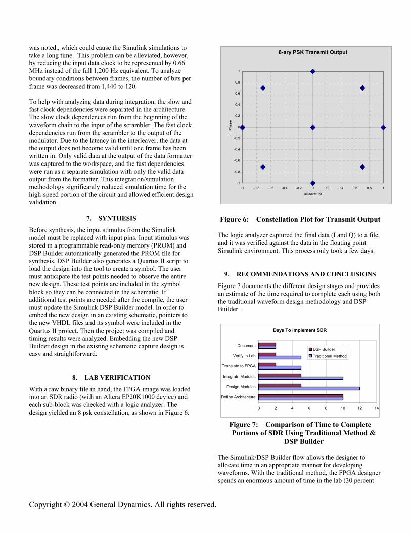
With a raw binary file in hand, the FPGA image was loaded into an SDR radio (with an Altera EP20K1000 device) and each sub-block was checked with a logic analyzer. The design yielded an 8 psk constellation, as shown in Figure 6.
8-ary PSK Transmit Output
-1
-0.8
-0.6
-0.4
-0.2
0
0.2
0.4
0.6
0.8
1
-1 -0.8 -0.6 -0.4 -0.2 0 0.2 0.4 0.6 0.8 1
Quadrature
In P
hase
Figure 6: Constellation Plot for Transmit Output
The logic analyzer captured the final data (I and Q) to a file, and it was verified against the data in the floating point Simulink environment. This process only took a few days.
9. RECOMMENDATIONS AND CONCLUSIONS
Figure 7 documents the different design stages and provides an estimate of the time required to complete each using both the traditional waveform design methodology and DSP Builder.
Days To Implement SDR
0 2 4 6 8 10 12 14
Define Architecture
Design Modules
Integrate Modules
Translate to FPGA
Verify in Lab
DocumentDSP Builder
Traditional Method
Figure 7: Comparison of Time to Complete Portions of SDR Using Traditional Method &
DSP Builder The Simulink/DSP Builder flow allows the designer to allocate time in an appropriate manner for developing waveforms. With the traditional method, the FPGA designer spends an enormous amount of time in the lab (30 percent
Copyright © 2004 General Dynamics. All rights reserved.
and up) troubleshooting FPGA design/system issues. The DSP Builder/Simulink/ModelSim simulation flow allows the designer to rapidly identify problems and troubleshoot them by adding appropriate taps and re-simulating the model. Taking simulations to a system integration level significantly reduces risks, time, and lab resources. Altera’s DSP Builder allows the hardware to be abstracted to a higher level so that the FPGA and system waveform developers can operate in a common environment or be one- in-the-same person. The tools have a very short learning curve if the user is familiar with Matlab/Simulink and hardware design. As the tool matures, some enhancements may be added to help speed up simulation times. One novel improvement is the addition of frame-based capability in all DSP Builder/Simulink blocks. This technique has been proven to speed up simulation times by many orders of magnitude in standard Matlab/Simulink. Given this capability, the system designer could build the Matlab/Simulink floating-point model using DSP Builder blocks initially, instead of having to use generic Simulink blocks. This would bypass the design flow step that translates the floating-point model into a fixed-point model. Another possible tool enhancement is a method for handling large clock disparities between the FPGA base clock and the model sample clocks. This paper describes a workaround to this dilemma, but there may be automated ways of simplifying this for the common user. The flow described has major advantages of streamlining validation, lab check-out, and providing a common environment within which multi-disciplined personnel can work and communicate. With its existing and upcoming features, DSP Builder is a powerful tool for rapidly developing SDR waveforms on FPGAs.