random number generator dmitriy solmonov w1-1 david levitt w1-2 jesse guss w1-3 sirisha pillalamarri...
TRANSCRIPT

Random Number Generator
Dmitriy Solmonov W1-1David Levitt W1-2Jesse Guss W1-3
Sirisha Pillalamarri W1-4 Matt Russo W1-5
Design Manager – Thiago Hersan
February 22, 2006Top Level Integration
Project Objective:Create a Cryptologically Secure Pseudo-Random Number Generator

Agenda• Status
• Design Decisions
• Timing Constraints
• Timing Analysis
• Power Analysis
• Registers

StatusCompleted C implementation Architecture Behavioral Design and Simulation Gate-Level Design and Simulation Preliminary FloorplanIn Progress Schematic Design and Simulation (90% Done) LayoutUnfinished• Extraction, LVS, post-layout simulation
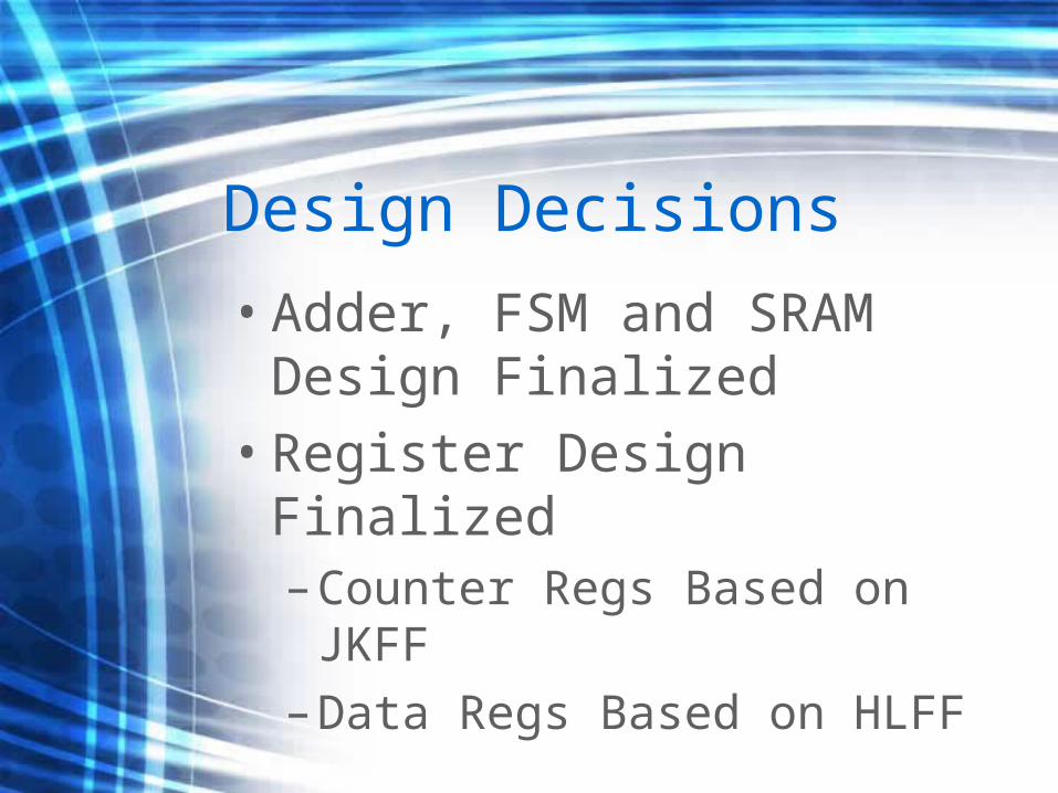
Design Decisions
• Adder, FSM and SRAM Design Finalized
• Register Design Finalized– Counter Regs Based on JKFF
– Data Regs Based on HLFF
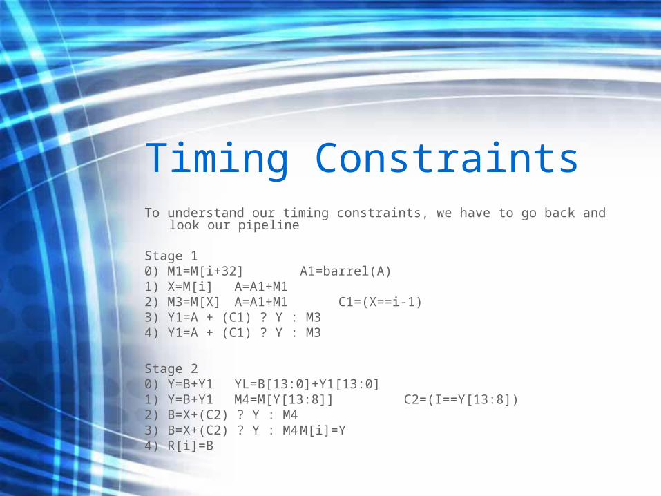
Timing ConstraintsTo understand our timing constraints, we have to go back and look our pipeline
Stage 10) M1=M[i+32] A1=barrel(A) 1) X=M[i] A=A1+M1 2) M3=M[X] A=A1+M1 C1=(X==i-1) 3) Y1=A + (C1) ? Y : M3 4) Y1=A + (C1) ? Y : M3
Stage 2 0) Y=B+Y1 YL=B[13:0]+Y1[13:0] 1) Y=B+Y1 M4=M[Y[13:8]] C2=(I==Y[13:8]) 2) B=X+(C2) ? Y : M4 3) B=X+(C2) ? Y : M4 M[i]=Y 4) R[i]=B

What does this mean?
• Since we have allotted the adder two ticks, the FSM one tick, and the SRAM half a tick…
• The adder’s propagation delay SHOULD be double that of the FSM, which has a propagation delay that SHOULD be double that of the SRAM

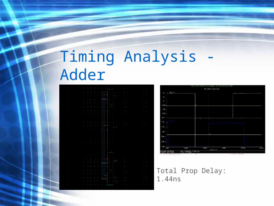
Timing Analysis - Adder
• Since our adder is so complicated we were unsure how to locate the critical path on the schematic by hand
• We found the critical path of the adder to be from the B[4] pin to the S[31] pin using Pathmill
Timing Analysis - Adder
Total Prop Delay:1.44ns
Timing Analysis - FSM
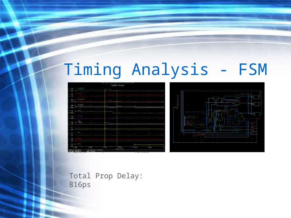
Total Prop Delay:816ps

Timing Analysis - SRAM
• The SRAM timing analysis had to happen in two parts.
• A test row and a test column were constructed to isolate different components of the SRAM
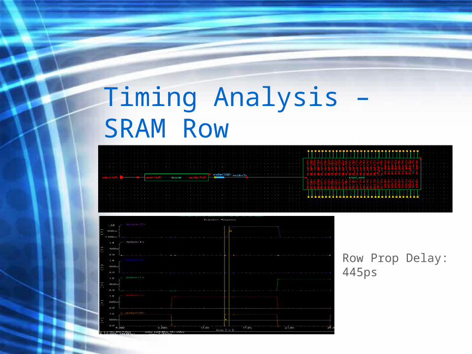
Timing Analysis – SRAM Row
Row Prop Delay:445ps
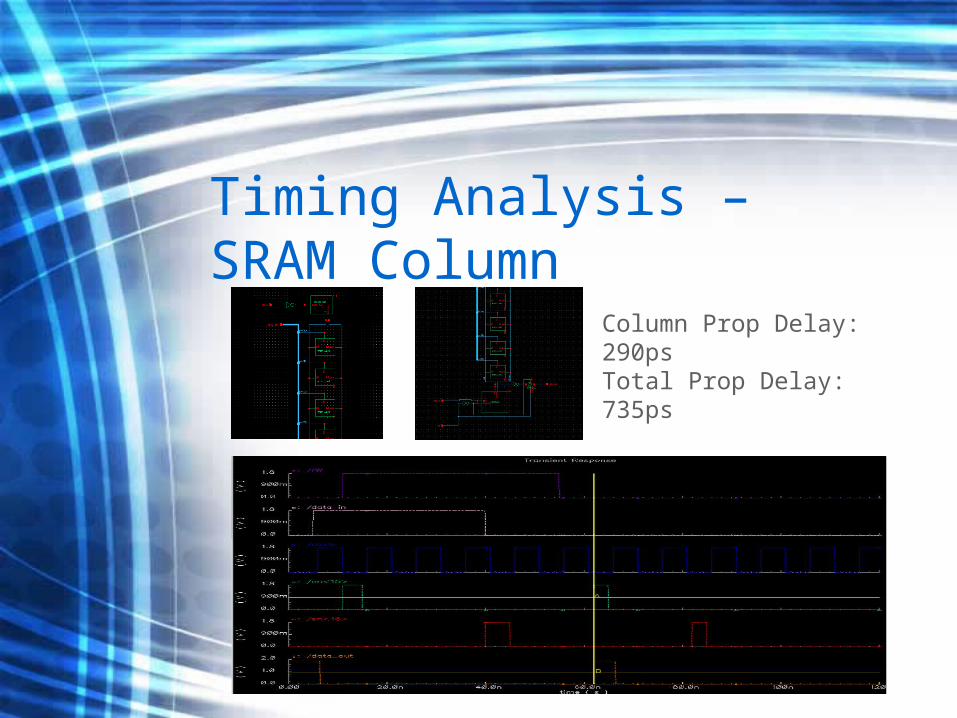
Timing Analysis – SRAM Column
Column Prop Delay:290psTotal Prop Delay:735ps
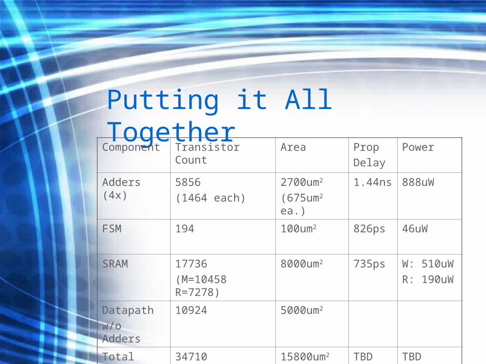
Putting it All TogetherComponent Transistor Count Area Prop
Delay
Power
Adders (4x) 5856
(1464 each)
2700um2
(675um2 ea.)
1.44ns 888uW
FSM 194 100um2 826ps 46uW
SRAM 17736
(M=10458 R=7278)
8000um2 735ps W: 510uW
R: 190uW
Datapath
w/o Adders
10924 5000um2
Total 34710 15800um2 TBD TBD
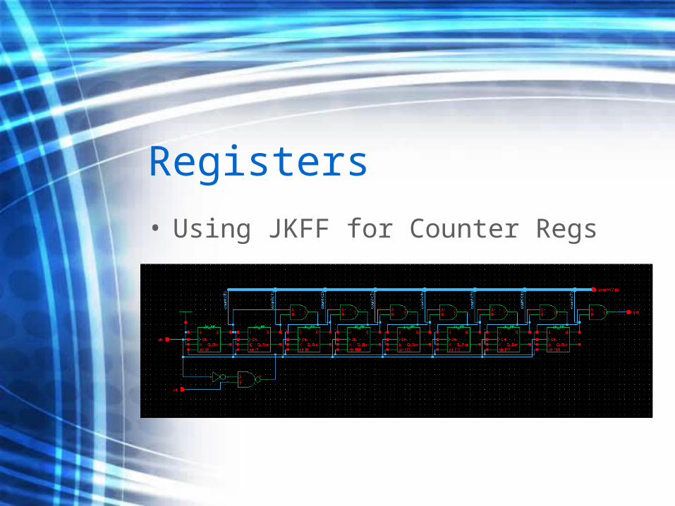
Registers
• Using JKFF for Counter Regs

Registers• Using HLFF for Data Regs
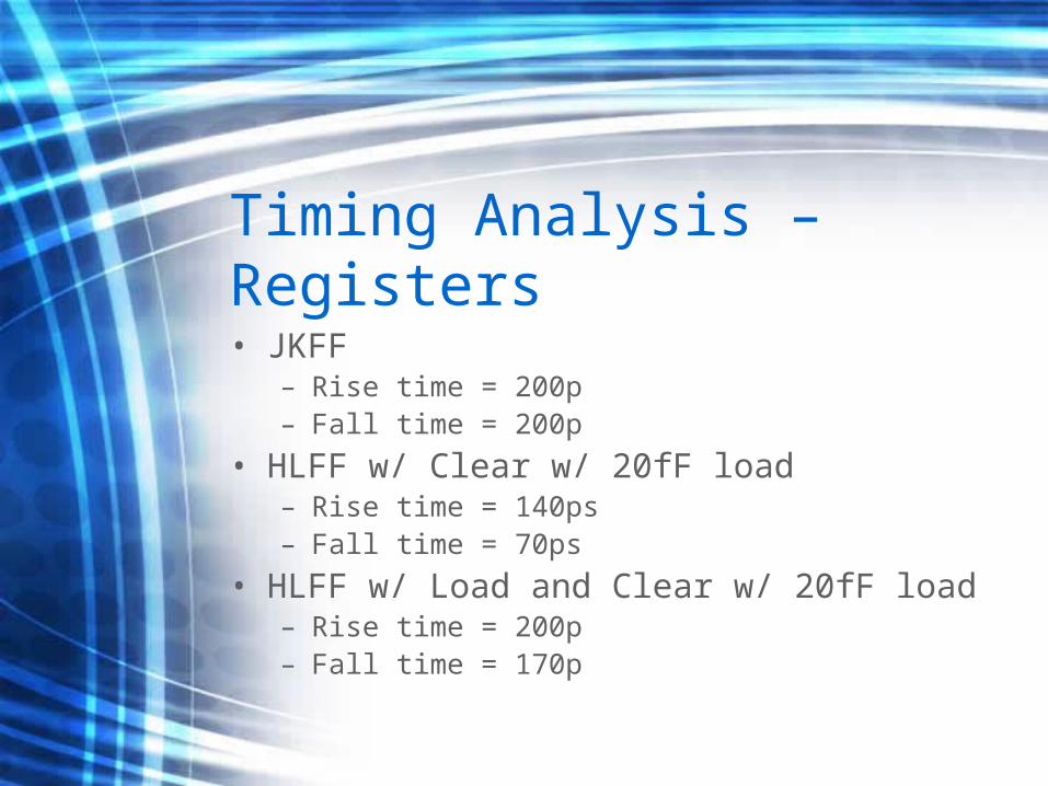
Timing Analysis – Registers• JKFF
– Rise time = 200p– Fall time = 200p
• HLFF w/ Clear w/ 20fF load– Rise time = 140ps– Fall time = 70ps
• HLFF w/ Load and Clear w/ 20fF load– Rise time = 200p – Fall time = 170p

Thanks!
Any Questions?