ram & rom based digital design
TRANSCRIPT

RAM & ROM Based Digital Design
ECE 152A – Winter 2012

March 12, 2012 ECE 152A - Digital Design Principles 2
Reading Assignment
Brown and Vranesic 10 Digital System Design
10.1 Building Block Circuits 10.1.3 Static Random Access Memory (SRAM) 10.1.4 SRAM Blocks in PLDs

March 12, 2012 ECE 152A - Digital Design Principles 3
Reading Assignment
Roth 9 Multiplexers, Decoders, and Programmable
Logic Devices 9.5 Read Only Memories

March 12, 2012 ECE 152A - Digital Design Principles 4
Read/Write Memories
RAM Random Access Memory
Same access time to all memory locations As opposed to serial access memory
About the same time for read and write SRAM
Static Random Access Memory Built with cross coupled inverters and pass transistors

March 12, 2012 ECE 152A - Digital Design Principles 5
Read/Write Memories
6T SRAM Cell CMOS implementation with pass transistors Sense amp at bottom of column

March 12, 2012 ECE 152A - Digital Design Principles 6
Read/Write Memories
RAM Blocks and Register Files
March 12, 2012 ECE 152A - Digital Design Principles 7
Read/Write Memories
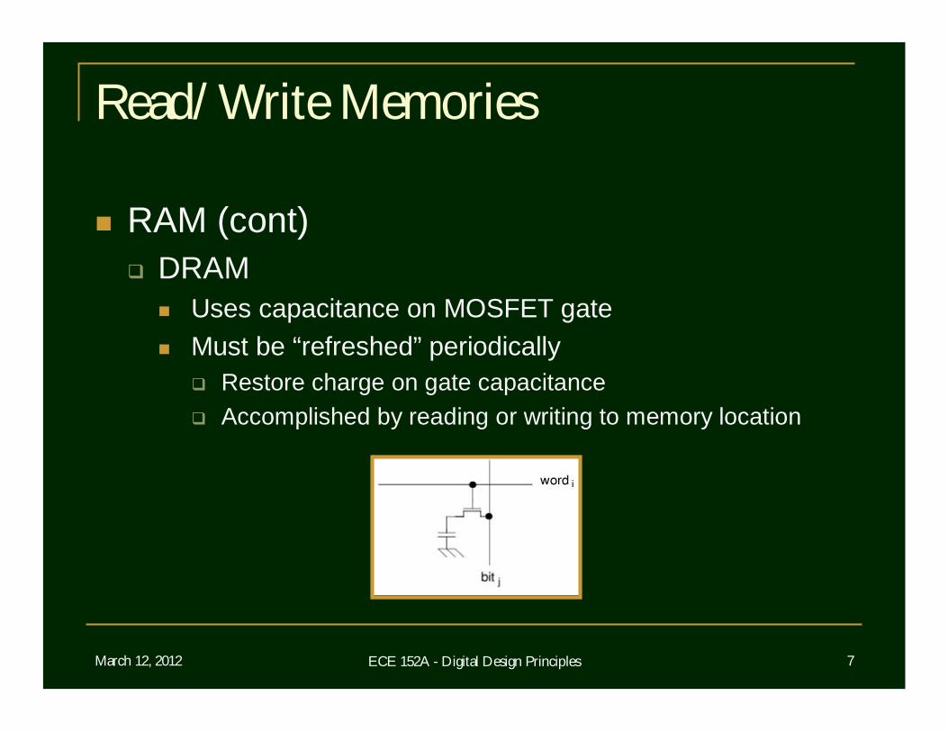
RAM (cont) DRAM
Uses capacitance on MOSFET gate Must be “refreshed” periodically
Restore charge on gate capacitance Accomplished by reading or writing to memory location

March 12, 2012 ECE 152A - Digital Design Principles 8
Read/Write Memories
RAM (cont) Both SRAM and DRAM are “volatile”
Data lost when power is removed DRAM has approximately 4 times the capacity of
SRAM Basic memory cell of DRAM is smaller
~2 transistors vs. 6
SRAM is generally faster

March 12, 2012 ECE 152A - Digital Design Principles 9
Read Only Memories
ROM, PROM, EPROM, EEPROM, EAROM Not in-system writeable
Except by special means, i.e. non-standard voltages and timing
“Non-volatile” Data retained when power removed
ROM : Read Only Memory Mask programmed by manufacturer Not erasable (programming permanent)
High volume applications

March 12, 2012 ECE 152A - Digital Design Principles 10
Read Only Memories
ROM, PROM, EPROM, EEPROM, EAROM PROM : Programmable Read Only Memory
Programmed by user Also not erasable
EPROM : Erasable Programmable Read Only Memory Programmed by user Erased using UV light
“erase” sets all bits to 0 or 1 Development applications

March 12, 2012 ECE 152A - Digital Design Principles 11
Read Only Memories
ROM, PROM, EPROM, EEPROM, EAROM EEPROM : Electrically Erasable Programmable
Read Only Memory Programmed by user Erased electrically
Possibly in system, but requires non-standard voltages
EAROM : Electrically Alterable Read Only Memory Similar to EEPROM

March 12, 2012 ECE 152A - Digital Design Principles 12
Read Mostly Memories
Flash memory Writable and non-volatile
Reads very fast Writes very slowly
Referred to as “programming”
No special voltages for in system writing “Flash” refers to the fact that the entire content of
the memory chip can be erased in one step Once erased and written, data is retained for 20+
years

March 12, 2012 ECE 152A - Digital Design Principles 13
Memory Structure
Array of memory cells Organization refers to number of and width of
memory words Example 1024 bit memory can organized as:
1024 one-bit word 512 two-bit words 256 four-bit words 128 eight-bit words
Internal array is the same for all organizations Decoding and I/O circuitry differs

March 12, 2012 ECE 152A - Digital Design Principles 14
Memory Structure
Memory Array and Address Decoder
March 12, 2012 ECE 152A - Digital Design Principles 15
Combinational Design with Memories
ROM (and RAM and Flash) is a “physical”truth table All addresses equal ≡ all inputs to logic network Each row of truth table corresponds to a single
address in the memory Example: 128 x 8 ROM
128, 8-bit words Log2 128 = 7 address bits (A6 – A0) 8 data bits D7 – D0 Can implement 7 input, 8 output function

March 12, 2012 ECE 152A - Digital Design Principles 16
Combinational Design with Memories
Binary to BCD converter with 128 x 8-bit ROM Addresses 0 – 99
Output equals 2 digit BCD number Addresses 100 – 127
All one’s, indicating invalid input

March 12, 2012 ECE 152A - Digital Design Principles 17
Combinational Design with Memories
ROM Contents Hex addresses 00 through 7F
Invalid1111 11117F
Invalid1111 111164
991001 100163
160001 011010
150001 01010F
010000 000101
000000 000000
Decimal ValueDataAddress

March 12, 2012 ECE 152A - Digital Design Principles 18
Combinational Design with Memories
Final Implementation

March 12, 2012 ECE 152A - Digital Design Principles 19
State Machine Design with Memories
For state machine, map state table directly into memory Address lines driven by present state and present
input Data outputs consist of next state and present
output Both Mealy and Moore machines can be realized
Output of Moore machine lags by one clock period (when state table directly mapped)

March 12, 2012 ECE 152A - Digital Design Principles 20
State Machine Design with Memories
Hardware Implementation
March 12, 2012 ECE 152A - Digital Design Principles 21
State Machine Design with Memories
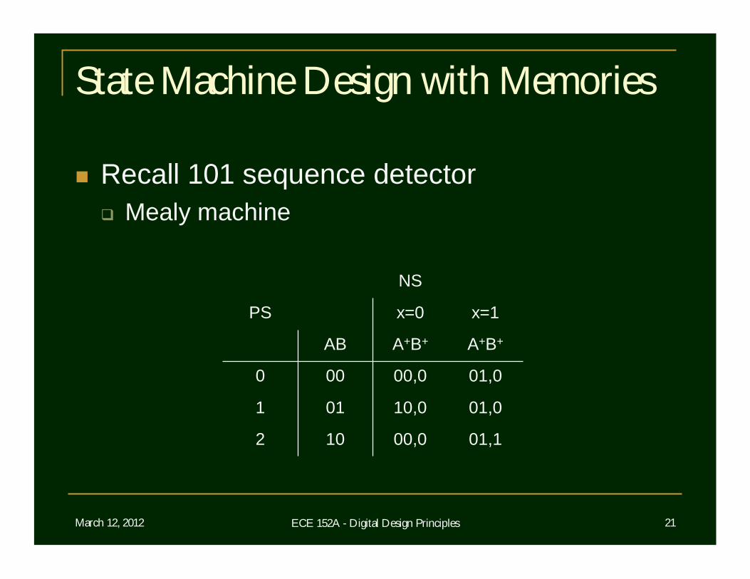
Recall 101 sequence detector Mealy machine
01,100,0102
01,010,0011
01,000,0000
A+B+A+B+AB
x=1x=0PS
NS

March 12, 2012 ECE 152A - Digital Design Principles 22
State Machine Design with Memories
ROM Contents (8 x 3-bit)
xxxx111xxxx011101110000010001101010001001100000000zNSxPS
DataAddress

March 12, 2012 ECE 152A - Digital Design Principles 23
State Machine Design with Memories
Timing Diagram

March 12, 2012 ECE 152A - Digital Design Principles 24
State Machine Design with Memories
101 sequence detector (again) Moore machine
01100102
10110113
00110011
00100000
ZA+B+A+B+AB
x=1x=0PS
NS
March 12, 2012 ECE 152A - Digital Design Principles 25
State Machine Design with Memories
Direct mapping of state table to memory Output lags by one clock period
Introduces latency to output timing “Pipelining” effect
Implement as “Mealy-like” machine Associate output with next state, not present state
All states have only one associated output (like Moore) Eliminates one clock-period latency
No longer “true” Moore machine