rail-to-rail input/output, 10 mhz ... - microchip...
TRANSCRIPT

© 2006 Microchip Technology Inc. DS21685C-page 1
MCP6021/1R/2/3/4
Features
• Rail-to-Rail Input/Output• Wide Bandwidth: 10 MHz (typ.)• Low Noise: 8.7 nV/√Hz, at 10 kHz (typ.)
• Low Offset Voltage:- Industrial Temperature: ±500 µV (max.)- Extended Temperature: ±250 µV (max.)
• Mid-Supply VREF: MCP6021 and MCP6023• Low Supply Current: 1 mA (typ.)
• Total Harmonic Distortion: 0.00053% (typ., G = 1)• Unity Gain Stable• Power Supply Range: 2.5V to 5.5V
• Temperature Range:- Industrial: -40°C to +85°C- Extended: -40°C to +125°C
Typical Applications
• Automotive
• Driving A/D Converters• Multi-Pole Active Filters• Barcode Scanners
• Audio Processing• Communications• DAC Buffer
• Test Equipment• Medical Instrumentation
Available Tools
• SPICE Macro Model (at www.microchip.com)• FilterLab® software (at www.microchip.com)
Typical Application
Description
The MCP6021, MCP6021R, MCP6022, MCP6023 andMCP6024 from Microchip Technology Inc. are rail-to-rail input and output op amps with high performance.Key specifications include: wide bandwidth (10 MHz),low noise (8.7 nV/√Hz), low input offset voltage and lowdistortion (0.00053% THD+N). The MCP6023 alsooffers a Chip Select pin (CS) that gives power savingswhen the part is not in use.
The single MCP6021 and MCP6021R are available inSOT-23-5. The single MCP6021, single MCP6023 anddual MCP6022 are available in 8-lead PDIP, SOIC andTSSOP. The Extended Temperature single MCP6021is available in 8-lead MSOP. The quad MCP6024 isoffered in 14-lead PDIP, SOIC and TSSOP packages.
The MCP6021/1R/2/3/4 family is available in Industrialand Extended temperature ranges. It has a powersupply range of 2.5V to 5.5V.
Package Types
PhotoDetector
100 pF
5.6 pF
100 kΩ
VDD/2
MCP6021
Transimpedance Amplifier
MCP6021SOT-23-5
1
2
3
5
4
VDD
VIN–
VOUT
VSS
VIN+
MCP6022PDIP SOIC, TSSOP
1
2
3
4
8
7
6
5
CS
VDD
VOUT
VREF
NC
VIN–
VIN+
VSS
MCP6023PDIP SOIC, TSSOP
1
2
3
4
8
7
6
5
VDD
VOUTB
VINB–
VINB+
VOUTA
VINA–
VINA+
VSS
MCP6024PDIP SOIC, TSSOP
1
2
3
4
VOUTD
VIND–
VIND+
VSS
VOUTA
VINA–
VINA+
VDD
VINC+
VINC–
VOUTC
5
6
7
VINB+
VINB–
VOUTB
14
13
12
11
10
9
8
MCP6021PDIP SOIC,
MSOP, TSSOP
1
2
3
4
8
7
6
5
NC
VDD
VOUT
VREF
NC
VIN–
VIN+
VSS
MCP6021RSOT-23-5
1
2
3
5
4
VSS
VIN–
VOUT
VDD
VIN+
Rail-to-Rail Input/Output, 10 MHz Op Amps
MCP6021/1R/2/3/4
DS21685C-page 2 © 2006 Microchip Technology Inc.
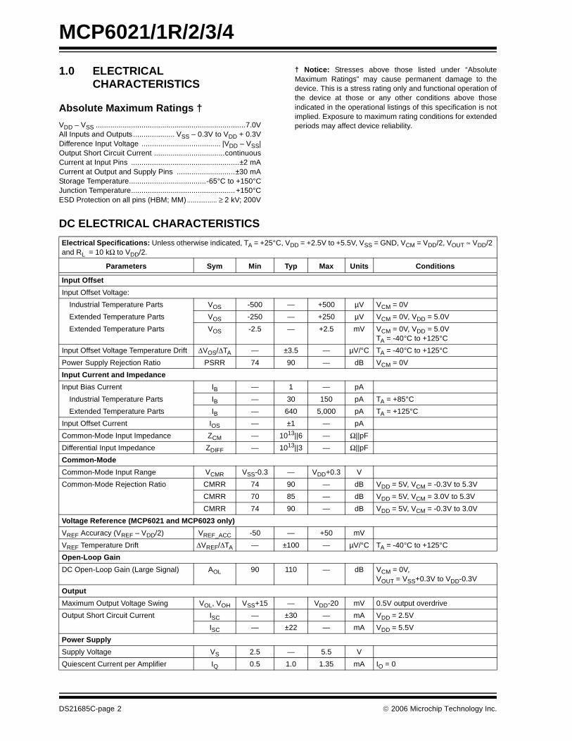
1.0 ELECTRICAL CHARACTERISTICS
Absolute Maximum Ratings †
VDD – VSS ........................................................................7.0VAll Inputs and Outputs.................... VSS – 0.3V to VDD + 0.3VDifference Input Voltage ...................................... |VDD – VSS|Output Short Circuit Current ..................................continuousCurrent at Input Pins ....................................................±2 mACurrent at Output and Supply Pins ............................±30 mAStorage Temperature.....................................-65°C to +150°CJunction Temperature..................................................+150°CESD Protection on all pins (HBM; MM) ................ ≥ 2 kV; 200V
† Notice: Stresses above those listed under “AbsoluteMaximum Ratings” may cause permanent damage to thedevice. This is a stress rating only and functional operation ofthe device at those or any other conditions above thoseindicated in the operational listings of this specification is notimplied. Exposure to maximum rating conditions for extendedperiods may affect device reliability.
DC ELECTRICAL CHARACTERISTICS
Electrical Specifications: Unless otherwise indicated, TA = +25°C, VDD = +2.5V to +5.5V, VSS = GND, VCM = VDD/2, VOUT ≈ VDD/2 and RL = 10 kΩ to VDD/2.
Parameters Sym Min Typ Max Units Conditions
Input Offset
Input Offset Voltage:
Industrial Temperature Parts VOS -500 — +500 µV VCM = 0V
Extended Temperature Parts VOS -250 — +250 µV VCM = 0V, VDD = 5.0V
Extended Temperature Parts VOS -2.5 — +2.5 mV VCM = 0V, VDD = 5.0VTA = -40°C to +125°C
Input Offset Voltage Temperature Drift ΔVOS/ΔTA — ±3.5 — µV/°C TA = -40°C to +125°C
Power Supply Rejection Ratio PSRR 74 90 — dB VCM = 0V
Input Current and Impedance
Input Bias Current IB — 1 — pA
Industrial Temperature Parts IB — 30 150 pA TA = +85°C
Extended Temperature Parts IB — 640 5,000 pA TA = +125°C
Input Offset Current IOS — ±1 — pA
Common-Mode Input Impedance ZCM — 1013||6 — Ω||pF
Differential Input Impedance ZDIFF — 1013||3 — Ω||pF
Common-Mode
Common-Mode Input Range VCMR VSS-0.3 — VDD+0.3 V
Common-Mode Rejection Ratio CMRR 74 90 — dB VDD = 5V, VCM = -0.3V to 5.3V
CMRR 70 85 — dB VDD = 5V, VCM = 3.0V to 5.3V
CMRR 74 90 — dB VDD = 5V, VCM = -0.3V to 3.0V
Voltage Reference (MCP6021 and MCP6023 only)
VREF Accuracy (VREF – VDD/2) VREF_ACC -50 — +50 mV
VREF Temperature Drift ΔVREF/ΔTA — ±100 — µV/°C TA = -40°C to +125°C
Open-Loop Gain
DC Open-Loop Gain (Large Signal) AOL 90 110 — dB VCM = 0V, VOUT = VSS+0.3V to VDD-0.3V
Output
Maximum Output Voltage Swing VOL, VOH VSS+15 — VDD-20 mV 0.5V output overdrive
Output Short Circuit Current ISC — ±30 — mA VDD = 2.5V
ISC — ±22 — mA VDD = 5.5V
Power Supply
Supply Voltage VS 2.5 — 5.5 V
Quiescent Current per Amplifier IQ 0.5 1.0 1.35 mA IO = 0

© 2006 Microchip Technology Inc. DS21685C-page 3
MCP6021/1R/2/3/4
AC ELECTRICAL CHARACTERISTICS
MCP6023 CHIP SELECT (CS) ELECTRICAL CHARACTERISTICS
Electrical Specifications: Unless otherwise indicated, TA = +25°C, VDD = +2.5V to +5.5V, VSS = GND, VCM = VDD/2, VOUT ≈ VDD/2, RL = 10 kΩ to VDD/2 and CL = 60 pF.
Parameters Sym Min Typ Max Units Conditions
AC Response
Gain Bandwidth Product GBWP — 10 — MHz
Phase Margin at Unity-Gain PM — 65 — ° G = +1
Settling Time, 0.2% tSETTLE — 250 — ns G = +1, VOUT = 100 mVp-p
Slew Rate SR — 7.0 — V/µs
Total Harmonic Distortion Plus Noise
f = 1 kHz, G = +1 V/V THD+N — 0.00053 — % VOUT = 0.25V to 3.25V (1.75V ± 1.50VPK), VDD = 5.0V, BW = 22 kHz
f = 1 kHz, G = +1 V/V, RL = 600Ω THD+N — 0.00064 — % VOUT = 0.25V to 3.25V (1.75V ± 1.50VPK), VDD = 5.0V, BW = 22 kHz
f = 1 kHz, G = +1 V/V THD+N — 0.0014 — % VOUT = 4VP-P, VDD = 5.0V, BW = 22 kHz
f = 1 kHz, G = +10 V/V THD+N — 0.0009 — % VOUT = 4VP-P, VDD = 5.0V, BW = 22 kHz
f = 1 kHz, G = +100 V/V THD+N — 0.005 — % VOUT = 4VP-P, VDD = 5.0V, BW = 22 kHz
Noise
Input Noise Voltage Eni — 2.9 — µVp-p f = 0.1 Hz to 10 Hz
Input Noise Voltage Density eni — 8.7 — nV/√Hz f = 10 kHz
Input Noise Current Density ini — 3 — fA/√Hz f = 1 kHz
Electrical Specifications: Unless otherwise indicated, TA = +25°C, VDD = +2.5V to +5.5V, VSS = GND, VCM = VDD/2, VOUT ≈ VDD/2, RL = 10 kΩ to VDD/2 and CL = 60 pF.
Parameters Sym Min Typ Max Units Conditions
CS Low Specifications
CS Logic Threshold, Low VIL VSS — 0.2 VDD V
CS Input Current, Low ICSL -1.0 0.01 — µA CS = VSS
CS High Specifications
CS Logic Threshold, High VIH 0.8 VDD — VDD V
CS Input Current, High ICSH — 0.01 2.0 µA CS = VDD
GND Current ISS -2 -0.05 — µA CS = VDD
Amplifier Output Leakage IO(LEAK) — 0.01 — µA CS = VDD
CS Dynamic Specifications
CS Low to Amplifier Output Turn-on Time tON — 2 10 µs G = +1, VIN = VSS, CS = 0.2VDD to VOUT = 0.45VDD time
CS High to Amplifier Output High-Z Time tOFF — 0.01 — µs G = +1, VIN = VSS, CS = 0.8VDD to VOUT = 0.05VDD time
Hysteresis VHYST — 0.6 — V VDD = 5.0V, Internal Switch

MCP6021/1R/2/3/4
DS21685C-page 4 © 2006 Microchip Technology Inc.
TEMPERATURE CHARACTERISTICS
FIGURE 1-1: Timing diagram for the CS pin on the MCP6023.
Electrical Specifications: Unless otherwise indicated, VDD = +2.5V to +5.5V and VSS = GND.
Parameters Sym Min Typ Max Units Conditions
Temperature Ranges
Industrial Temperature Range TA -40 — +85 °C
Extended Temperature Range TA -40 — +125 °C
Operating Temperature Range TA -40 — +125 °C Note 1
Storage Temperature Range TA -65 — +150 °C
Thermal Package Resistances
Thermal Resistance, 5L-SOT-23 θJA — 256 — °C/W
Thermal Resistance, 8L-PDIP θJA — 85 — °C/W
Thermal Resistance, 8L-SOIC θJA — 163 — °C/W
Thermal Resistance, 8L-MSOP θJA — 206 — °C/W
Thermal Resistance, 8L-TSSOP θJA — 124 — °C/W
Thermal Resistance, 14L-PDIP θJA — 70 — °C/W
Thermal Resistance, 14L-SOIC θJA — 120 — °C/W
Thermal Resistance, 14L-TSSOP θJA — 100 — °C/W
Note 1: The industrial temperature devices operate over this extended temperature range, but with reduced performance. In any case, the internal junction temperature (TJ) must not exceed the absolute maximum specification of 150°C.
High-Z
tON
CS
tOFF
VOUT
-50 nA (typ.)
High-Z
ISS
ICS 10 nA (typ.) 10 nA (typ.) 10 nA (typ.)
-50 nA (typ.)-1 mA (typ.)
Amplifier On

© 2006 Microchip Technology Inc. DS21685C-page 5
MCP6021/1R/2/3/4
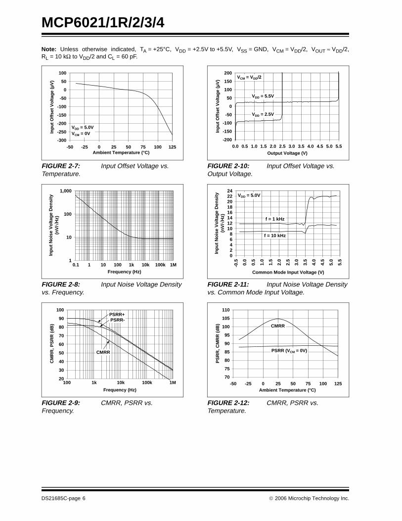
2.0 TYPICAL PERFORMANCE CURVES
Note: Unless otherwise indicated, TA = +25°C, VDD = +2.5V to +5.5V, VSS = GND, VCM = VDD/2, VOUT ≈ VDD/2,RL = 10 kΩ to VDD/2 and CL = 60 pF.
FIGURE 2-1: Input Offset Voltage, (Industrial Temperature Parts).
FIGURE 2-2: Input Offset Voltage, (Extended Temperature Parts).
FIGURE 2-3: Input Offset Voltage vs. Common Mode Input Voltage with VDD = 2.5V.
FIGURE 2-4: Input Offset Voltage Drift, (Industrial Temperature Parts).
FIGURE 2-5: Input Offset Voltage Drift, (Extended Temperature Parts).
FIGURE 2-6: Input Offset Voltage vs. Common Mode Input Voltage with VDD = 5.5V.
Note: The graphs and tables provided following this note are a statistical summary based on a limited number ofsamples and are provided for informational purposes only. The performance characteristics listed hereinare not tested or guaranteed. In some graphs or tables, the data presented may be outside the specifiedoperating range (e.g., outside specified power supply range) and therefore outside the warranted range.
0%
2%
4%
6%
8%
10%
12%
14%
16%
-500
-400
-300
-200
-100 0
100
200
300
400
500
Input Offset Voltage (µV)
Per
cen
tag
e o
f O
ccu
ran
ces 1192 Samples
VCM = 0VTA = +25°C
I-TempParts
0%2%4%6%8%
10%12%14%16%18%20%22%24%
-240
-200
-160
-120 -80
-40 0 40 80 120
160
200
240
Input Offset Voltage (µV)
Per
cen
tag
e o
f O
ccu
ran
ces 438 Samples
VDD = 5.0VVCM = 0VTA = +25°C
E-TempParts
-500-400-300-200-100
0100200300400500
-0.5 0.0 0.5 1.0 1.5 2.0 2.5 3.0
Common Mode Input Voltage (V)
Inp
ut
Off
set
Vo
ltag
e (µ
V) VDD = 2.5V
-40°C+25°C+85°C+125°C
0%2%4%6%8%
10%12%14%16%18%20%22%24%
-20
-16
-12 -8 -4 0 4 8 12 16 20
Input Offset Voltage Drift (µV/°C)
Per
cen
tag
e o
f O
ccu
ran
ces 1192 Samples
VCM = 0VTA = -40°C to +85°C
I-TempParts
0%2%4%6%8%
10%12%14%16%18%20%22%24%
-20
-16
-12 -8 -4 0 4 8 12 16 20
Input Offset Voltage Drift (µV/°C)
Per
cen
tag
e o
f O
ccu
ran
ces 438 Samples
VCM = 0VTA = -40°C to +125°C
E-TempParts
-500-400-300-200-100
0100200300400500
-0.5 0.0
0.5
1.0
1.5
2.0
2.5
3.0
3.5
4.0
4.5
5.0
5.5
6.0
Common Mode Input Voltage (V)
Inp
ut
Off
set
Vo
ltag
e (µ
V) VDD = 5.5V -40°C
+25°C+85°C+125°C
MCP6021/1R/2/3/4
DS21685C-page 6 © 2006 Microchip Technology Inc.
Note: Unless otherwise indicated, TA = +25°C, VDD = +2.5V to +5.5V, VSS = GND, VCM = VDD/2, VOUT ≈ VDD/2,RL = 10 kΩ to VDD/2 and CL = 60 pF.
FIGURE 2-7: Input Offset Voltage vs. Temperature.
FIGURE 2-8: Input Noise Voltage Density vs. Frequency.
FIGURE 2-9: CMRR, PSRR vs. Frequency.
FIGURE 2-10: Input Offset Voltage vs. Output Voltage.
FIGURE 2-11: Input Noise Voltage Density vs. Common Mode Input Voltage.
FIGURE 2-12: CMRR, PSRR vs. Temperature.
-300
-250
-200
-150
-100
-50
0
50
100
-50 -25 0 25 50 75 100 125Ambient Temperature (°C)
Inp
ut
Off
set
Vo
ltag
e (µ
V)
VDD = 5.0VVCM = 0V
1
10
100
1,000
1.E-01 1.E+00 1.E+01 1.E+02 1.E+03 1.E+04 1.E+05 1.E+06
Frequency (Hz)
Inp
ut
No
ise
Vo
ltag
e D
ensi
ty
(nV
/ √H
z)
0.1 1 10 100 1k 10k 1M100k
20
30
40
50
60
70
80
90
100
1.E+02 1.E+03 1.E+04 1.E+05 1.E+06
Frequency (Hz)
CM
RR
, PS
RR
(d
B)
PSRR+PSRR-
CMRR
100 1k 10k 100k 1M
-200
-150
-100
-50
0
50
100
150
200
0.0 0.5 1.0 1.5 2.0 2.5 3.0 3.5 4.0 4.5 5.0 5.5
Output Voltage (V)
Inp
ut
Off
set
Vo
ltag
e (µ
V)
VDD = 5.5V
VCM = VDD/2
VDD = 2.5V
02468
1012141618202224
-0.5 0.0
0.5
1.0
1.5
2.0
2.5
3.0
3.5
4.0
4.5
5.0
5.5
Common Mode Input Voltage (V)
Inp
ut
No
ise
Vo
ltag
e D
ensi
ty
(nV
/ √H
z)
VDD = 5.0V
f = 1 kHz
f = 10 kHz
70
75
80
85
90
95
100
105
110
-50 -25 0 25 50 75 100 125Ambient Temperature (°C)
PS
RR
, CM
RR
(d
B)
PSRR (VCM = 0V)
CMRR

© 2006 Microchip Technology Inc. DS21685C-page 7
MCP6021/1R/2/3/4
Note: Unless otherwise indicated, TA = +25°C, VDD = +2.5V to +5.5V, VSS = GND, VCM = VDD/2, VOUT ≈ VDD/2,RL = 10 kΩ to VDD/2 and CL = 60 pF.
FIGURE 2-13: Input Bias, Offset Currents vs. Common Mode Input Voltage.
FIGURE 2-14: Quiescent Current vs. Supply Voltage.
FIGURE 2-15: Output Short-Circuit Current vs. Supply Voltage.
FIGURE 2-16: Input Bias, Offset Currents vs. Temperature.
FIGURE 2-17: Quiescent Current vs. Temperature.
FIGURE 2-18: Open-Loop Gain, Phase vs. Frequency.
1
10
100
1,000
10,000
0.0 0.5 1.0 1.5 2.0 2.5 3.0 3.5 4.0 4.5 5.0 5.5Common Mode Input Voltage (V)
Inp
ut
Bia
s, O
ffse
t C
urr
ents
(p
A)
IB, TA = +125°CVDD = 5.5V
IOS, TA = +85°C
IOS, TA = +125°C
IB, TA = +85°C
0.00.10.20.30.40.50.60.70.80.91.01.11.2
0.0 0.5 1.0 1.5 2.0 2.5 3.0 3.5 4.0 4.5 5.0 5.5Power Supply Voltage (V)
Qu
iesc
ent
Cu
rren
t (m
A/a
mp
lifie
r)
+125°C+85°C+25°C-40°C
0
5
10
15
20
25
30
35
0.0 0.5 1.0 1.5 2.0 2.5 3.0 3.5 4.0 4.5 5.0 5.5Supply Voltage (V)
Ou
tpu
t S
ho
rt C
ircu
it C
urr
ent
(mA
)
+125°C+85°C+25°C-40°C
1
10
100
1,000
10,000
25 35 45 55 65 75 85 95 105 115 125
Ambient Temperature (°C)
Inp
ut
Bia
s, O
ffse
t C
urr
ents
(p
A)
IB
VCM = VDD
VDD = 5.5V
IOS
0.00.10.20.30.40.50.60.70.80.91.01.11.2
-50 -25 0 25 50 75 100 125Ambient Temperature (°C)
Qu
iesc
ent
Cu
rren
t (m
A/a
mp
lifie
r)
VDD = 5.5V
VDD = 2.5V
VCM = VDD - 0.5V
-20-10
0102030405060708090
100110120
1.E+00 1.E+01 1.E+02 1.E+03 1.E+04 1.E+05 1.E+06 1.E+07 1.E+08
Frequency (Hz)
Op
en-L
oo
p G
ain
(d
B)
-210-195-180-165-150-135-120-105-90-75-60-45-30-150
Op
en-L
oo
p P
has
e (°
)
Gain
Phase
1 10010 1k 100k10k 1M 100M10M

MCP6021/1R/2/3/4
DS21685C-page 8 © 2006 Microchip Technology Inc.
Note: Unless otherwise indicated, TA = +25°C, VDD = +2.5V to +5.5V, VSS = GND, VCM = VDD/2, VOUT ≈ VDD/2,RL = 10 kΩ to VDD/2 and CL = 60 pF.
FIGURE 2-19: DC Open-Loop Gain vs. Load Resistance.
FIGURE 2-20: Small Signal DC Open-Loop Gain vs. Output Voltage Headroom.
FIGURE 2-21: Gain Bandwidth Product, Phase Margin vs. Temperature.
FIGURE 2-22: DC Open-Loop Gain vs. Temperature.
FIGURE 2-23: Gain Bandwidth Product, Phase Margin vs. Common Mode Input Voltage.
FIGURE 2-24: Gain Bandwidth Product, Phase Margin vs. Output Voltage.
80
90
100
110
120
130
1.E+02 1.E+03 1.E+04 1.E+05
Load Resistance (Ω)
DC
Op
en-L
oo
p G
ain
(d
B) VDD = 5.5V
VDD = 2.5V
100 1k 10k 100k
70
80
90
100
110
120
0.00 0.05 0.10 0.15 0.20 0.25 0.30
Output Voltage Headroom (V);VDD - VOH or VOL - VSS
DC
Op
en-L
oo
p G
ain
(d
B)
VCM = VDD/2
VDD = 2.5V
VDD = 5.5V
0123456789
10
-50 -25 0 25 50 75 100 125Ambient Temperature (°C)
Gai
n B
and
wid
th P
rod
uct
(M
Hz)
0102030405060708090100
Ph
ase
Mar
gin
, G =
+1
(°)
GBWP, VDD = 5.5VGBWP, VDD = 2.5VPM, VDD = 2.5VPM, VDD = 5.5V
90
95
100
105
110
115
120
-50 -25 0 25 50 75 100 125Ambient Temperature (°C)
DC
Op
en-L
oo
p G
ain
(d
B)
VDD = 5.5V
VDD = 2.5V
0
2
4
6
8
10
12
14
0.0 0.5 1.0 1.5 2.0 2.5 3.0 3.5 4.0 4.5 5.0Common Mode Input Voltage (V)
Gai
n B
and
wid
th P
rod
uct
(M
Hz)
0
15
30
45
60
75
90
105
Ph
ase
Mar
gin
, G =
+1
(°)Gain Bandwidth Product
Phase Margin, G = +1
VDD = 5.0V
0
2
4
6
8
10
12
14
0.0 0.5 1.0 1.5 2.0 2.5 3.0 3.5 4.0 4.5 5.0Output Voltage (V)
Gai
n B
and
wid
th P
rod
uct
(M
Hz)
0
15
30
45
60
75
90
105
Ph
ase
Mar
gin
, G =
+1
(°)
Gain Bandwidth Product
Phase Margin, G = +1
VDD = 5.0VVCM = VDD/2

© 2006 Microchip Technology Inc. DS21685C-page 9
MCP6021/1R/2/3/4
Note: Unless otherwise indicated, TA = +25°C, VDD = +2.5V to +5.5V, VSS = GND, VCM = VDD/2, VOUT ≈ VDD/2,RL = 10 kΩ to VDD/2 and CL = 60 pF.
FIGURE 2-25: Slew Rate vs. Temperature.
FIGURE 2-26: Total Harmonic Distortion plus Noise vs. Output Voltage with f = 1 kHz.
FIGURE 2-27: The MCP6021/1R/2/3/4 family shows no phase reversal under overdrive.
FIGURE 2-28: Maximum Output Voltage Swing vs. Frequency.
FIGURE 2-29: Total Harmonic Distortion plus Noise vs. Output Voltage with f = 20 kHz.
FIGURE 2-30: Channel-to-Channel Separation vs. Frequency (MCP6022 and MCP6024 only).
0123456789
1011
-50 -25 0 25 50 75 100 125Ambient Temperature (°C)
Sle
w R
ate
(V/µ
s)
Falling, VDD = 2.5VRising, VDD = 2.5V
Falling, VDD = 5.5VRising, VDD = 5.5V
0.0001%
0.0010%
0.0100%
0.1000%
0.0 0.5 1.0 1.5 2.0 2.5 3.0 3.5 4.0 4.5 5.0Output Voltage (VP-P)
TH
D+N
(%
)
f = 1 kHzBWMeas = 22 kHzVDD = 5.0V
G = +1 V/V
G = +10 V/V
G = +100 V/V
-1
0
1
2
3
4
5
6
0 10 20 30 40 50 60 70 80 90 100Time (10 µs/div)
Inp
ut,
Ou
tpu
t V
olt
age
(V) VDD = 5.0V
G = +2 V/V
VIN
VOUT
0.1
1
10
1.E+04 1.E+05 1.E+06 1.E+07
Frequency (Hz)
Max
imu
m O
utp
ut
Vo
ltag
e S
win
g (
VP
-P)
VDD = 5.5V
10k 100k 1M 10M
VDD = 2.5V
0.0001%
0.0010%
0.0100%
0.1000%
0.0 0.5 1.0 1.5 2.0 2.5 3.0 3.5 4.0 4.5 5.0Output Voltage (VP-P)
TH
D+N
(%
) G = +10 V/V
f = 20 kHzBWMeas = 80 kHzVDD = 5.0V
G = +1 V/V
G = +100 V/V
105
110
115
120
125
130
135
1.E+03 1.E+04 1.E+05 1.E+06
Frequency (Hz)
Ch
ann
el t
o C
han
nel
Sep
arat
ion
(d
B)
1k 1M100k10k
G = +1 V/V
MCP6021/1R/2/3/4
DS21685C-page 10 © 2006 Microchip Technology Inc.
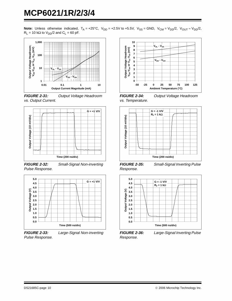
Note: Unless otherwise indicated, TA = +25°C, VDD = +2.5V to +5.5V, VSS = GND, VCM = VDD/2, VOUT ≈ VDD/2,RL = 10 kΩ to VDD/2 and CL = 60 pF.
FIGURE 2-31: Output Voltage Headroom vs. Output Current.
FIGURE 2-32: Small-Signal Non-inverting Pulse Response.
FIGURE 2-33: Large-Signal Non-inverting Pulse Response.
FIGURE 2-34: Output Voltage Headroom vs. Temperature.
FIGURE 2-35: Small-Signal Inverting Pulse Response.
FIGURE 2-36: Large-Signal Inverting Pulse Response.
1
10
100
1,000
0.01 0.1 1 10Output Current Magnitude (mA)
Ou
tpu
t V
olt
age
Hea
dro
om
;V
DD-V
OH o
r V
OL-V
SS (
mV
)
VDD - VOH
VOL - VSS
-6.E-02
-5.E-02
-4.E-02
-3.E-02
-2.E-02
-1.E-02
0.E+00
1.E-02
2.E-02
3.E-02
4.E-02
5.E-02
6.E-02
0.E+00 2.E-07 4.E-07 6.E-07 8.E-07 1.E-06 1.E-06 1.E-06 2.E-06 2.E-06 2.E-06
Time (200 ns/div)
Ou
tpu
t V
olt
age
(10
mV
/div
)
G = +1 V/V
0.0
0.5
1.0
1.5
2.0
2.5
3.0
3.5
4.0
4.5
5.0
0.E+00 5.E-07 1.E-06 2.E-06 2.E-06 3.E-06 3.E-06 4.E-06 4.E-06 5.E-06 5.E-06
Time (500 ns/div)
Ou
tpu
t V
olt
age
(V)
G = +1 V/V
0123456789
10
-50 -25 0 25 50 75 100 125Ambient Temperature (°C)
Ou
tpu
t V
olt
age
Hea
dro
om
VD
D-V
OH o
r V
OL-V
SS (
mV
)
VDD - VOH
VOL - VSS
-6.E-02
-5.E-02
-4.E-02
-3.E-02
-2.E-02
-1.E-02
0.E+00
1.E-02
2.E-02
3.E-02
4.E-02
5.E-02
6.E-02
0.E+00 2.E-07 4.E-07 6.E-07 8.E-07 1.E-06 1.E-06 1.E-06 2.E-06 2.E-06 2.E-06
Time (200 ns/div)
Ou
tpu
t V
olt
age
(10
mV
/div
)
G = -1 V/VRF = 1 kΩ
0.0
0.5
1.0
1.5
2.0
2.5
3.0
3.5
4.0
4.5
5.0
0.E+00 5.E-07 1.E-06 2.E-06 2.E-06 3.E-06 3.E-06 4.E-06 4.E-06 5.E-06 5.E-06
Time (500 ns/div)
Ou
tpu
t V
olt
age
(V)
G = -1 V/VRF = 1 kΩ

© 2006 Microchip Technology Inc. DS21685C-page 11
MCP6021/1R/2/3/4
Note: Unless otherwise indicated, TA = +25°C, VDD = +2.5V to +5.5V, VSS = GND, VCM = VDD/2, VOUT ≈ VDD/2,RL = 10 kΩ to VDD/2 and CL = 60 pF.
FIGURE 2-37: VREF Accuracy vs. Supply Voltage (MCP6021 and MCP6023 only).
FIGURE 2-38: Chip Select (CS) Hysteresis (MCP6023 only) with VDD = 2.5V.
FIGURE 2-39: Chip Select (CS) to Amplifier Output Response Time (MCP6023 only).
FIGURE 2-40: VREF Accuracy vs. Temperature (MCP6021 and MCP6023 only).
FIGURE 2-41: Chip Select (CS) Hysteresis (MCP6023 only) with VDD = 5.5V.
-50-40-30-20-10
01020304050
0.0 0.5 1.0 1.5 2.0 2.5 3.0 3.5 4.0 4.5 5.0 5.5Power Supply Voltage (V)
VR
EF A
ccu
racy
; V
RE
F –
VD
D/2
(mV
)
0.0
0.2
0.4
0.6
0.8
1.0
1.2
1.4
1.6
0.0 0.5 1.0 1.5 2.0 2.5Chip Select Voltage (V)
Qu
iesc
ent
Cu
rren
t (m
A/a
mp
lifie
r)
Op Ampshuts off here
Op Ampturns on here
Hysteresis
VDD = 2.5VG = +1 V/VVIN = 1.25V
CS sweptlow to high
CS swepthigh to low
-0.50.00.51.01.52.02.53.03.54.04.55.05.5
0.0E+00 5.0E-06 1.0E-05 1.5E-05 2.0E-05 2.5E-05 3.0E-05 3.5E-05
Time (5 µs/div)
Ch
ip S
elec
t V
olt
age,
Ou
tpu
t V
olt
age
(V)
Output High-Z
VDD = 5.0VG = +1 V/VVIN = VSS
Outputon
Outputon
VOUT
CS Voltage
-50-40-30-20-10
01020304050
-50 -25 0 25 50 75 100 125Ambient Temperature (°C)
VR
EF A
ccu
racy
; V
RE
F –
VD
D/2
(mV
)
VDD = 5.5V
VDD = 2.5V
Representative Part
0.0
0.2
0.4
0.6
0.8
1.0
1.2
1.4
1.6
0.0 0.5 1.0 1.5 2.0 2.5 3.0 3.5 4.0 4.5 5.0 5.5
Chip Select Voltage (V)
Qu
iesc
ent
Cu
rren
t (m
A/a
mp
lifie
r)
Op Ampshuts off here
Op Ampturns on here
HysteresisCS swepthigh to low
CS sweptlow to highVDD = 5.5V
G = +1 V/VVIN = 2.75V
MCP6021/1R/2/3/4
DS21685C-page 12 © 2006 Microchip Technology Inc.
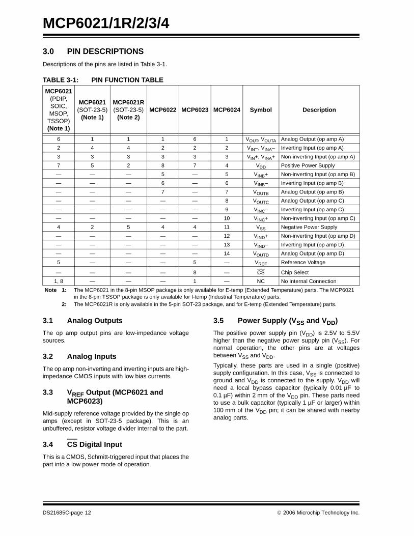
3.0 PIN DESCRIPTIONS
Descriptions of the pins are listed in Table 3-1.
TABLE 3-1: PIN FUNCTION TABLE
3.1 Analog Outputs
The op amp output pins are low-impedance voltagesources.
3.2 Analog Inputs
The op amp non-inverting and inverting inputs are high-impedance CMOS inputs with low bias currents.
3.3 VREF Output (MCP6021 and MCP6023)
Mid-supply reference voltage provided by the single opamps (except in SOT-23-5 package). This is anunbuffered, resistor voltage divider internal to the part.
3.4 CS Digital Input
This is a CMOS, Schmitt-triggered input that places thepart into a low power mode of operation.
3.5 Power Supply (VSS and VDD)
The positive power supply pin (VDD) is 2.5V to 5.5Vhigher than the negative power supply pin (VSS). Fornormal operation, the other pins are at voltagesbetween VSS and VDD.
Typically, these parts are used in a single (positive)supply configuration. In this case, VSS is connected toground and VDD is connected to the supply. VDD willneed a local bypass capacitor (typically 0.01 µF to0.1 µF) within 2 mm of the VDD pin. These parts needto use a bulk capacitor (typically 1 µF or larger) within100 mm of the VDD pin; it can be shared with nearbyanalog parts.
MCP6021(PDIP,SOIC,MSOP,
TSSOP)(Note 1)
MCP6021(SOT-23-5)
(Note 1)
MCP6021R(SOT-23-5)
(Note 2)MCP6022 MCP6023 MCP6024 Symbol Description
6 1 1 1 6 1 VOUT, VOUTA Analog Output (op amp A)
2 4 4 2 2 2 VIN–, VINA– Inverting Input (op amp A)
3 3 3 3 3 3 VIN+, VINA+ Non-inverting Input (op amp A)
7 5 2 8 7 4 VDD Positive Power Supply
— — — 5 — 5 VINB+ Non-inverting Input (op amp B)
— — — 6 — 6 VINB– Inverting Input (op amp B)
— — — 7 — 7 VOUTB Analog Output (op amp B)
— — — — — 8 VOUTC Analog Output (op amp C)
— — — — — 9 VINC– Inverting Input (op amp C)
— — — — — 10 VINC+ Non-inverting Input (op amp C)
4 2 5 4 4 11 VSS Negative Power Supply
— — — — — 12 VIND+ Non-inverting Input (op amp D)
— — — — — 13 VIND– Inverting Input (op amp D)
— — — — — 14 VOUTD Analog Output (op amp D)
5 — — — 5 — VREF Reference Voltage
— — — — 8 — CS Chip Select
1, 8 — — — 1 — NC No Internal Connection
Note 1: The MCP6021 in the 8-pin MSOP package is only available for E-temp (Extended Temperature) parts. The MCP6021 in the 8-pin TSSOP package is only available for I-temp (Industrial Temperature) parts.
2: The MCP6021R is only available in the 5-pin SOT-23 package, and for E-temp (Extended Temperature) parts.
© 2006 Microchip Technology Inc. DS21685C-page 13
MCP6021/1R/2/3/4
4.0 APPLICATIONS INFORMATION
The MCP6021/1R/2/3/4 family of operational amplifiersare fabricated on Microchip’s state-of-the-art CMOSprocess. They are unity-gain stable and suitable for awide range of general-purpose applications.
4.1 Rail-to-Rail Input
The MCP6021/1R/2/3/4 amplifier family is designed tonot exhibit phase inversion when the input pins exceedthe supply voltages. Figure 2-27 shows an input volt-age exceeding both supplies with no resulting phaseinversion.
The input stage of the MCP6021/1R/2/3/4 family ofdevices uses two differential input stages in parallel;one operates at low common-mode input voltage(VCM), while the other operates at high VCM. With thistopology, the device operates with VCM up to 0.3V pasteither supply rail (VSS – 0.3V to VDD + 0.3V) at +25°C.The amplifier input behaves linearly as long as VCM iskept within the specified VCMR limits. The input offsetvoltage is measured at both VCM = VSS – 0.3V andVDD + 0.3V to ensure proper operation.
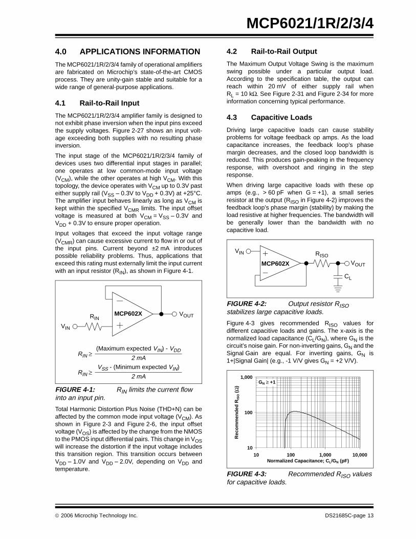
Input voltages that exceed the input voltage range(VCMR) can cause excessive current to flow in or out ofthe input pins. Current beyond ±2 mA introducespossible reliability problems. Thus, applications thatexceed this rating must externally limit the input currentwith an input resistor (RIN), as shown in Figure 4-1.
FIGURE 4-1: RIN limits the current flow into an input pin.
Total Harmonic Distortion Plus Noise (THD+N) can beaffected by the common mode input voltage (VCM). Asshown in Figure 2-3 and Figure 2-6, the input offsetvoltage (VOS) is affected by the change from the NMOSto the PMOS input differential pairs. This change in VOSwill increase the distortion if the input voltage includesthis transition region. This transition occurs betweenVDD – 1.0V and VDD – 2.0V, depending on VDD andtemperature.
4.2 Rail-to-Rail Output
The Maximum Output Voltage Swing is the maximumswing possible under a particular output load.According to the specification table, the output canreach within 20 mV of either supply rail whenRL = 10 kΩ. See Figure 2-31 and Figure 2-34 for moreinformation concerning typical performance.
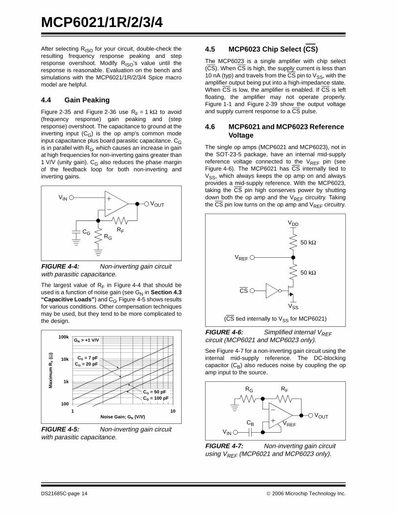
4.3 Capacitive Loads
Driving large capacitive loads can cause stabilityproblems for voltage feedback op amps. As the loadcapacitance increases, the feedback loop’s phasemargin decreases, and the closed loop bandwidth isreduced. This produces gain-peaking in the frequencyresponse, with overshoot and ringing in the stepresponse.
When driving large capacitive loads with these opamps (e.g., > 60 pF when G = +1), a small seriesresistor at the output (RISO in Figure 4-2) improves thefeedback loop’s phase margin (stability) by making theload resistive at higher frequencies. The bandwidth willbe generally lower than the bandwidth with nocapacitive load.
FIGURE 4-2: Output resistor RISO stabilizes large capacitive loads.
Figure 4-3 gives recommended RISO values fordifferent capacitive loads and gains. The x-axis is thenormalized load capacitance (CL/GN), where GN is thecircuit’s noise gain. For non-inverting gains, GN and theSignal Gain are equal. For inverting gains, GN is1+|Signal Gain| (e.g., -1 V/V gives GN = +2 V/V).
FIGURE 4-3: Recommended RISO values for capacitive loads.
VIN
RINVOUTMCP602X
RIN ≥(Maximum expected VIN) - VDD
2 mA
RIN ≥VSS - (Minimum expected VIN)
2 mA
VIN
MCP602X
RISO
VOUT
CL
10
100
1,000
10 100 1,000 10,000Normalized Capacitance; CL/GN (pF)
Rec
om
men
ded
RIS
O (
Ω)
GN ≥ +1
MCP6021/1R/2/3/4
DS21685C-page 14 © 2006 Microchip Technology Inc.
After selecting RISO for your circuit, double-check theresulting frequency response peaking and stepresponse overshoot. Modify RISO’s value until theresponse is reasonable. Evaluation on the bench andsimulations with the MCP6021/1R/2/3/4 Spice macromodel are helpful.
4.4 Gain Peaking
Figure 2-35 and Figure 2-36 use RF = 1 kΩ to avoid(frequency response) gain peaking and (stepresponse) overshoot. The capacitance to ground at theinverting input (CG) is the op amp’s common modeinput capacitance plus board parasitic capacitance. CGis in parallel with RG, which causes an increase in gainat high frequencies for non-inverting gains greater than1 V/V (unity gain). CG also reduces the phase marginof the feedback loop for both non-inverting andinverting gains.
FIGURE 4-4: Non-inverting gain circuit with parasitic capacitance.
The largest value of RF in Figure 4-4 that should beused is a function of noise gain (see GN in Section 4.3“Capacitive Loads”) and CG. Figure 4-5 shows resultsfor various conditions. Other compensation techniquesmay be used, but they tend to be more complicated tothe design.
FIGURE 4-5: Non-inverting gain circuit with parasitic capacitance.
4.5 MCP6023 Chip Select (CS)
The MCP6023 is a single amplifier with chip select(CS). When CS is high, the supply current is less than10 nA (typ) and travels from the CS pin to VSS, with theamplifier output being put into a high-impedance state.When CS is low, the amplifier is enabled. If CS is leftfloating, the amplifier may not operate properly.Figure 1-1 and Figure 2-39 show the output voltageand supply current response to a CS pulse.
4.6 MCP6021 and MCP6023 Reference Voltage
The single op amps (MCP6021 and MCP6023), not inthe SOT-23-5 package, have an internal mid-supplyreference voltage connected to the VREF pin (seeFigure 4-6). The MCP6021 has CS internally tied toVSS, which always keeps the op amp on and alwaysprovides a mid-supply reference. With the MCP6023,taking the CS pin high conserves power by shuttingdown both the op amp and the VREF circuitry. Takingthe CS pin low turns on the op amp and VREF circuitry.
FIGURE 4-6: Simplified internal VREF circuit (MCP6021 and MCP6023 only).
See Figure 4-7 for a non-inverting gain circuit using theinternal mid-supply reference. The DC-blockingcapacitor (CB) also reduces noise by coupling the opamp input to the source.
FIGURE 4-7: Non-inverting gain circuit using VREF (MCP6021 and MCP6023 only).
VIN
RG
RF
VOUT
CG
1.E+02
1.E+03
1.E+04
1.E+05
1 10Noise Gain; GN (V/V)
Max
imu
m R
F (
Ω)
GN > +1 V/V
100
1k
10k
100k
CG = 7 pFCG = 20 pF
CG = 50 pFCG = 100 pF
VDD
VSS
VREF
CS
50 kΩ
50 kΩ
(CS tied internally to VSS for MCP6021)
VIN
RG RF
VOUTCB VREF

© 2006 Microchip Technology Inc. DS21685C-page 15
MCP6021/1R/2/3/4
To use the internal mid-supply reference for aninverting gain circuit, connect the VREF pin to thenon-inverting input, as shown in Figure 4-8. Thecapacitor CB helps reduce power supply noise on theoutput.
FIGURE 4-8: Inverting gain circuit using VREF (MCP6021 and MCP6023 only).
If you don’t need the mid-supply reference, leave theVREF pin open.
4.7 Supply Bypass
With this family of operational amplifiers, the powersupply pin (VDD for single supply) should have a localbypass capacitor (i.e., 0.01 µF to 0.1 µF) within 2 mmfor good, high-frequency performance. It also needs abulk capacitor (i.e., 1 µF or larger) within 100 mm toprovide large, slow currents. This bulk capacitor can beshared with nearby analog parts.
4.8 Unused Op Amps
An unused op amp in a quad package (MCP6024)should be configured as shown in Figure 4-9. Thesecircuits prevent the output from toggling and causingcrosstalk. Circuit A can use any reference voltagebetween the supplies, provides a buffered DC voltage,and minimizes the supply current draw of the unusedop amp. Circuit B uses the minimum number of compo-nents and operates as a comparator; it may draw morecurrent.
FIGURE 4-9: Unused Op Amps.
4.9 PCB Surface Leakage
In applications where low input bias current is critical,PCB (printed circuit board) surface-leakage effectsneed to be considered. Surface leakage is caused byhumidity, dust or other contamination on the board.Under low humidity conditions, a typical resistancebetween nearby traces is 1012Ω. A 5V difference wouldcause 5 pA of current to flow, which is greater than theMCP6021/1R/2/3/4 family’s bias current at +25°C(1 pA, typ).
The easiest way to reduce surface leakage is to use aguard ring around sensitive pins (or traces). The guardring is biased at the same voltage as the sensitive pin.Figure 4-10 shows an example of this type of layout.
FIGURE 4-10: Example Guard Ring Layout.
1. Non-inverting Gain and Unity-Gain Buffer.a) Connect the guard ring to the inverting input
pin (VIN–); this biases the guard ring to thecommon mode input voltage.
b) Connect the non-inverting pin (VIN+) to theinput with a wire that does not touch thePCB surface.
2. Inverting (Figure 4-10) and TransimpedanceGain Amplifiers (convert current to voltage, suchas photo detectors).a) Connect the guard ring to the non-inverting
input pin (VIN+). This biases the guard ringto the same reference voltage as the opamp’s input (e.g., VDD/2 or ground).
b) Connect the inverting pin (VIN–) to the inputwith a wire that does not touch the PCBsurface.
4.10 High Speed PCB Layout
Due to their speed capabilities, a little extra care in thePCB (Printed Circuit Board) layout can make asignificant difference in the performance of these opamps. Good PC board layout techniques will help youachieve the performance shown in Section 1.0 “Elec-trical Characteristics” and Section 2.0 “Typical Per-formance Curves”, while also helping you minimizeEMC (Electro-Magnetic Compatibility) issues.
Use a solid ground plane and connect the bypass localcapacitor(s) to this plane with minimal length traces.This cuts down inductive and capacitive crosstalk.
VIN
RG RF
VOUT
VREF
CB
VDD
VDD
¼ MCP6144 (A) ¼ MCP6144 (B)
R
R
VDD
Guard Ring VIN– VIN+

MCP6021/1R/2/3/4
DS21685C-page 16 © 2006 Microchip Technology Inc.
Separate digital from analog, low speed from highspeed and low power from high power. This will reduceinterference.
Keep sensitive traces short and straight. Separatingthem from interfering components and traces. This isespecially important for high-frequency (low rise-time)signals.
Sometimes it helps to place guard traces next to victimtraces. They should be on both sides of the victimtrace, and as close as possible. Connect the guardtrace to ground plane at both ends, and in the middlefor long traces.
Use coax cables (or low inductance wiring) to routesignal and power to and from the PCB.
4.11 Typical Applications
4.11.1 A/D CONVERTER DRIVER AND ANTI-ALIASING FILTER
Figure 4-11 shows a third-order Butterworth filter thatcan be used as an A/D converter driver. It has a band-width of 20 kHz and a reasonable step response. It willwork well for conversion rates of 80 ksps and greater (ithas 29 dB attenuation at 60 kHz).
FIGURE 4-11: A/D converter driver and anti-aliasing filter with a 20 kHz cutoff frequency.
This filter can easily be adjusted to another bandwidthby multiplying all capacitors by the same factor.Alternatively, the resistors can all be scaled by anothercommon factor to adjust the bandwidth.
4.11.2 OPTICAL DETECTOR AMPLIFIER
Figure 4-12 shows the MCP6021 op amp used as atransimpedance amplifier in a photo detector circuit.The photo detector looks like a capacitive currentsource, so the 100 kΩ resistor gains the input signal toa reasonable level. The 5.6 pF capacitor stabilizes thiscircuit and produces a flat frequency response with abandwidth of 370 kHz.
FIGURE 4-12: Transimpedance Amplifier for an Optical Detector.
14.7 kΩ 33.2 kΩ
1.0 nF
100 pF
MCP602X8.45 kΩ
1.2 nF
PhotoDetector
100 pF
5.6 pF
100 kΩ
VDD/2
MCP6021
© 2006 Microchip Technology Inc. DS21685C-page 17
MCP6021/1R/2/3/4
5.0 DESIGN TOOLS
Microchip provides the basic design tools needed forthe MCP6021/1R/2/3/4 family of op amps.
5.1 SPICE Macro Model
The latest SPICE macro model available for theMCP6021/1R/2/3/4 op amps is on Microchip’s web siteat www.microchip.com. This model is intended as aninitial design tool that works well in the op amp’s linearregion of operation at room temperature. Within themacro model file is information on its capabilities.
Bench testing is a very important part of any design andcannot be replaced with simulations. Also, simulationresults using this macro model need to be validated bycomparing them to the data sheet specifications andcharacteristic curves.
5.2 FilterLab® Software
Microchip’s FilterLab® software is an innovative toolthat simplifies analog active filter (using op amps)design. It is available free of charge from our web siteat www.microchip.com. The FilterLab software toolprovides full schematic diagrams of the filter circuit withcomponent values. It also outputs the filter circuit inSPICE format, which can be used with the macromodel to simulate actual filter performance.

MCP6021/1R/2/3/4
DS21685C-page 18 © 2006 Microchip Technology Inc.
6.0 PACKAGING INFORMATION
6.1 Package Marking Information
Legend: XX...X Customer-specific informationY Year code (last digit of calendar year)YY Year code (last 2 digits of calendar year)WW Week code (week of January 1 is week ‘01’)NNN Alphanumeric traceability code Pb-free JEDEC designator for Matte Tin (Sn)* This package is Pb-free. The Pb-free JEDEC designator ( )
can be found on the outer packaging for this package.
Note: In the event the full Microchip part number cannot be marked on one line, it willbe carried over to the next line, thus limiting the number of availablecharacters for customer-specific information.
3e
3e
5-Lead SOT-23 (MCP6021/MCP6021R) Example: (E-temp)
XXNN EY25Device E-Temp Code
MCP6021 EYNN
MCP6021R EZNN
Note: Applies to 5-Lead SOT-23
XXXXXXXXXXXXXNNN
YYWW
8-Lead PDIP (300 mil) Example:
MCP6021I/P256
0331
MCP6021E/P^^256
0549OR 3e
8-Lead SOIC (150 mil) Example:
XXXXXXXXXXXXYYWW
NNN
MCP6021I/SN0331
256
MCP6021ESN^^0549
256OR 3e
8-Lead MSOP Example:
XXXXXX
YWWNNN
6021E
549256
8-Lead TSSOP Example:
XXXX
YYWW
NNN
6021
E549
256
© 2006 Microchip Technology Inc. DS21685C-page 19
MCP6021/1R/2/3/4
Package Marking Information (Continued)
14-Lead PDIP (300 mil) (MCP6024) Example:
14-Lead TSSOP (MCP6024) Example:
14-Lead SOIC (150 mil) (MCP6024) Example:
XXXXXXXXXXXXXXXXXXXXXXXXXXXX
YYWWNNN
XXXXXXXXXX
YYWWNNN
XXXXXXYYWW
NNN
MCP6024-I/PXXXXXXXXXXXXXX
0331256
6024E0331
256
XXXXXXXXXXMCP6024ISL
0331256
XXXXXXXXXX
MCP6024E/P^^
0549256OR
MCP6024
0549256
E/SL^^OR
3e
3e
MCP6021/1R/2/3/4
DS21685C-page 20 © 2006 Microchip Technology Inc.
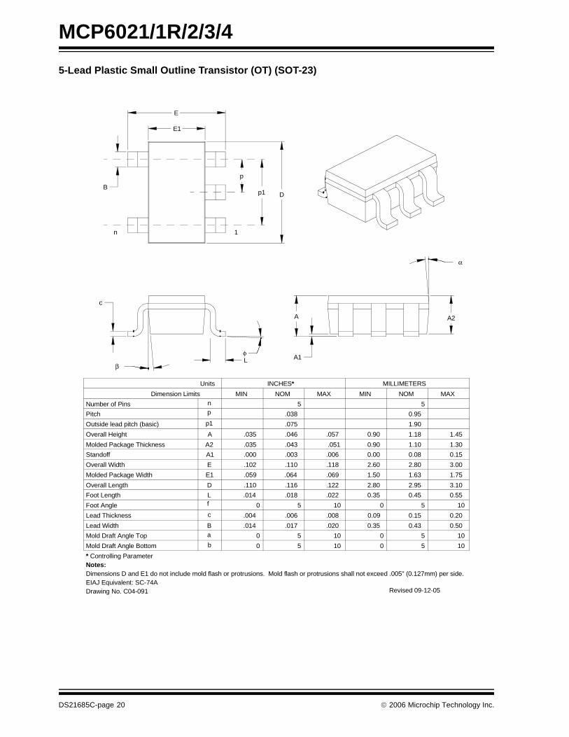
5-Lead Plastic Small Outline Transistor (OT) (SOT-23)
1
p
DB
n
E
E1
L
c
β
φ
α
A2A
A1
p1
10501050bMold Draft Angle Bottom
10501050aMold Draft Angle Top
0.500.430.35.020.017.014BLead Width
0.200.150.09.008.006.004cLead Thickness
10501050fFoot Angle
0.550.450.35.022.018.014LFoot Length
3.102.952.80.122.116.110DOverall Length
1.751.631.50.069.064.059E1Molded Package Width
3.002.802.60.118.110.102EOverall Width
0.150.080.00.006.003.000A1Standoff
1.301.100.90.051.043.035A2Molded Package Thickness
1.451.180.90.057.046.035AOverall Height
1.90.075p1Outside lead pitch (basic)
0.95.038pPitch
55nNumber of Pins
MAXNOMMINMAXNOMMINDimension Limits
MILLIMETERSINCHES*Units
Dimensions D and E1 do not include mold flash or protrusions. Mold flash or protrusions shall not exceed .005" (0.127mm) per side.Notes:
EIAJ Equivalent: SC-74ADrawing No. C04-091
* Controlling Parameter
Revised 09-12-05

© 2006 Microchip Technology Inc. DS21685C-page 21
MCP6021/1R/2/3/4
8-Lead Plastic Dual In-line (P) – 300 mil (PDIP)
B1
B
A1
A
L
A2
p
α
E
eB
β
c
E1
n
D
1
2
Units INCHES* MILLIMETERSDimension Limits MIN NOM MAX MIN NOM MAX
Number of Pins n 8 8Pitch p .100 2.54Top to Seating Plane A .140 .155 .170 3.56 3.94 4.32Molded Package Thickness A2 .115 .130 .145 2.92 3.30 3.68Base to Seating Plane A1 .015 0.38Shoulder to Shoulder Width E .300 .313 .325 7.62 7.94 8.26Molded Package Width E1 .240 .250 .260 6.10 6.35 6.60Overall Length D .360 .373 .385 9.14 9.46 9.78Tip to Seating Plane L .125 .130 .135 3.18 3.30 3.43Lead Thickness c .008 .012 .015 0.20 0.29 0.38Upper Lead Width B1 .045 .058 .070 1.14 1.46 1.78Lower Lead Width B .014 .018 .022 0.36 0.46 0.56Overall Row Spacing § eB .310 .370 .430 7.87 9.40 10.92Mold Draft Angle Top α 5 10 15 5 10 15Mold Draft Angle Bottom β 5 10 15 5 10 15* Controlling Parameter
Notes:Dimensions D and E1 do not include mold flash or protrusions. Mold flash or protrusions shall not exceed
JEDEC Equivalent: MS-001Drawing No. C04-018
.010” (0.254mm) per side.
§ Significant Characteristic
MCP6021/1R/2/3/4
DS21685C-page 22 © 2006 Microchip Technology Inc.
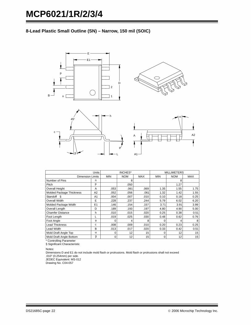
8-Lead Plastic Small Outline (SN) – Narrow, 150 mil (SOIC)
Foot Angle φ 0 4 8 0 4 8
1512015120βMold Draft Angle Bottom1512015120αMold Draft Angle Top
0.510.420.33.020.017.013BLead Width0.250.230.20.010.009.008cLead Thickness
0.760.620.48.030.025.019LFoot Length0.510.380.25.020.015.010hChamfer Distance5.004.904.80.197.193.189DOverall Length3.993.913.71.157.154.146E1Molded Package Width6.206.025.79.244.237.228EOverall Width0.250.180.10.010.007.004A1Standoff §1.551.421.32.061.056.052A2Molded Package Thickness1.751.551.35.069.061.053AOverall Height
1.27.050pPitch88nNumber of Pins
MAXNOMMINMAXNOMMINDimension LimitsMILLIMETERSINCHES*Units
2
1
D
n
p
B
E
E1
h
Lβ
c
45°
φ
A2
α
A
A1
* Controlling Parameter
Notes:Dimensions D and E1 do not include mold flash or protrusions. Mold flash or protrusions shall not exceed .010” (0.254mm) per side.JEDEC Equivalent: MS-012Drawing No. C04-057
§ Significant Characteristic
© 2006 Microchip Technology Inc. DS21685C-page 23
MCP6021/1R/2/3/4
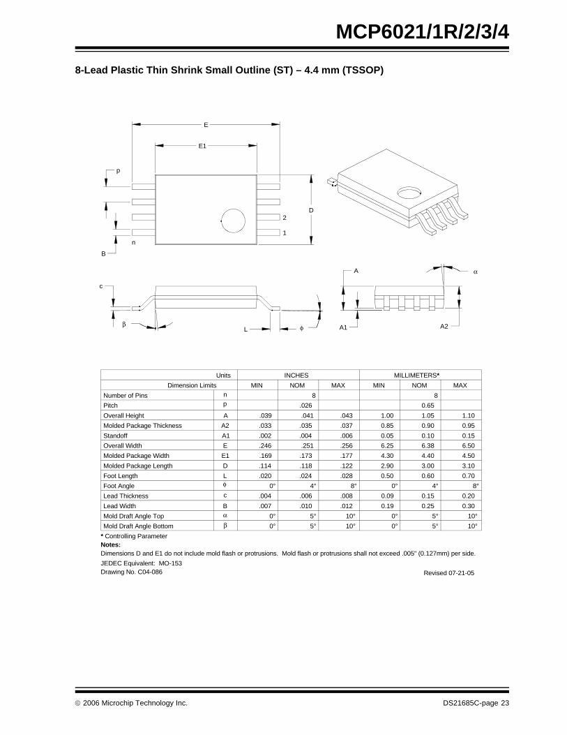
8-Lead Plastic Thin Shrink Small Outline (ST) – 4.4 mm (TSSOP)
α
A2
A
A1L
c
β φ
1
2D
n
p
B
E
E1
10°5°0°10°5°0°βMold Draft Angle Bottom
10°5°0°10°5°0°αMold Draft Angle Top
0.300.250.19.012.010.007BLead Width
0.200.150.09.008.006.004cLead Thickness
0.700.600.50.028.024.020LFoot Length
3.103.002.90.122.118.114DMolded Package Length
4.504.404.30.177.173.169E1Molded Package Width
6.506.386.25.256.251.246EOverall Width
0.150.100.05.006.004.002A1Standoff
0.950.900.85.037.035.033A2Molded Package Thickness
1.101.051.00.043.041.039AOverall Height
0.65.026pPitch
88nNumber of Pins
MAXNOMMINMAXNOMMINDimension Limits
MILLIMETERS*INCHESUnits
Foot Angle φ 0° 4° 8° 0° 4° 8°
Dimensions D and E1 do not include mold flash or protrusions. Mold flash or protrusions shall not exceed .005" (0.127mm) per side.Notes:
JEDEC Equivalent: MO-153
Revised 07-21-05
* Controlling Parameter
Drawing No. C04-086
MCP6021/1R/2/3/4
DS21685C-page 24 © 2006 Microchip Technology Inc.
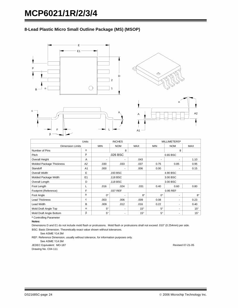
8-Lead Plastic Micro Small Outline Package (MS) (MSOP)
D
A
A1L
c
α
A2
E1
E
p
B n 1
2
φ
β
F
Dimensions D and E1 do not include mold flash or protrusions. Mold flash or protrusions shall not exceed .010" (0.254mm) per side.
.037 REFFFootprint (Reference)
Notes:
Revised 07-21-05
* Controlling Parameter
Mold Draft Angle Top
Mold Draft Angle Bottom
Foot Angle
Lead Width
Lead Thickness
β
α
c
B
φ
.003
.009
.006
.012
Dimension Limits
Overall Height
Molded Package Thickness
Molded Package Width
Overall Length
Foot Length
Standoff
Overall Width
Number of Pins
Pitch
A
L
E1
D
A1
E
A2
.016 .024
.118 BSC
.118 BSC
.000
.030
.193 BSC
.033
MIN
p
n
Units
.026 BSC
NOM
8
INCHES
0.95 REF
-
-
.009
.016
0.08
0.22
0°
0.23
0.40
8°
MILLIMETERS*
0.65 BSC
0.85
3.00 BSC
3.00 BSC
0.60
4.90 BSC
.043
.031
.037
.006
0.40
0.00
0.75
MINMAX NOM
1.10
0.80
0.15
0.95
MAX
8
- -
-
15°5° -
15°5° -
JEDEC Equivalent: MO-187
0° - 8°
5°
5° -
-
15°
15°
--
- -
BSC: Basic Dimension. Theoretically exact value shown without tolerances.
REF: Reference Dimension, usually without tolerance, for information purposes only.See ASME Y14.5M
See ASME Y14.5M
Drawing No. C04-111

© 2006 Microchip Technology Inc. DS21685C-page 25
MCP6021/1R/2/3/4
14-Lead Plastic Dual In-line (P) – 300 mil (PDIP)
E1
n
D
1
2
eB
β
E
c
A
A1
B
B1
L
A2
p
α
Units INCHES* MILLIMETERSDimension Limits MIN NOM MAX MIN NOM MAX
Number of Pins n 14 14Pitch p .100 2.54Top to Seating Plane A .140 .155 .170 3.56 3.94 4.32Molded Package Thickness A2 .115 .130 .145 2.92 3.30 3.68Base to Seating Plane A1 .015 0.38Shoulder to Shoulder Width E .300 .313 .325 7.62 7.94 8.26Molded Package Width E1 .240 .250 .260 6.10 6.35 6.60Overall Length D .740 .750 .760 18.80 19.05 19.30Tip to Seating Plane L .125 .130 .135 3.18 3.30 3.43Lead Thickness c .008 .012 .015 0.20 0.29 0.38Upper Lead Width B1 .045 .058 .070 1.14 1.46 1.78Lower Lead Width B .014 .018 .022 0.36 0.46 0.56Overall Row Spacing § eB .310 .370 .430 7.87 9.40 10.92Mold Draft Angle Top α 5 10 15 5 10 15
β 5 10 15 5 10 15Mold Draft Angle Bottom* Controlling Parameter
Notes:Dimensions D and E1 do not include mold flash or protrusions. Mold flash or protrusions shall not exceed .010” (0.254mm) per side.JEDEC Equivalent: MS-001Drawing No. C04-005
§ Significant Characteristic
MCP6021/1R/2/3/4
DS21685C-page 26 © 2006 Microchip Technology Inc.
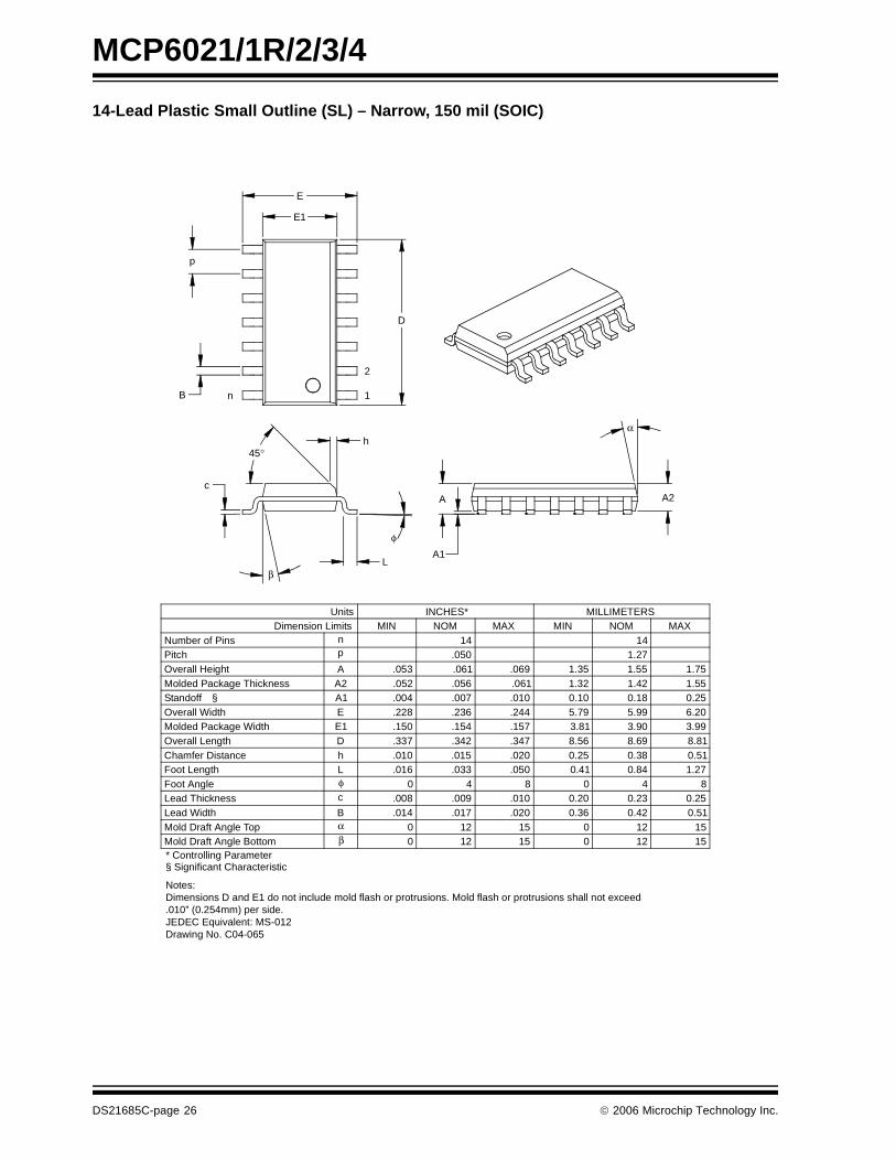
14-Lead Plastic Small Outline (SL) – Narrow, 150 mil (SOIC)
Foot Angle φ 0 4 8 0 4 8
1512015120βMold Draft Angle Bottom1512015120αMold Draft Angle Top
0.510.420.36.020.017.014BLead Width0.250.230.20.010.009.008cLead Thickness
1.270.840.41.050.033.016LFoot Length0.510.380.25.020.015.010hChamfer Distance8.818.698.56.347.342.337DOverall Length3.993.903.81.157.154.150E1Molded Package Width6.205.995.79.244.236.228EOverall Width0.250.180.10.010.007.004A1Standoff §1.551.421.32.061.056.052A2Molded Package Thickness1.751.551.35.069.061.053AOverall Height
1.27.050pPitch1414nNumber of Pins
MAXNOMMINMAXNOMMINDimension LimitsMILLIMETERSINCHES*Units
2
1
D
p
nB
E
E1
h
L
c
β
45°
φ
α
A2A
A1
* Controlling Parameter
Notes:Dimensions D and E1 do not include mold flash or protrusions. Mold flash or protrusions shall not exceed .010” (0.254mm) per side.JEDEC Equivalent: MS-012Drawing No. C04-065
§ Significant Characteristic

© 2006 Microchip Technology Inc. DS21685C-page 27
MCP6021/1R/2/3/4
14-Lead Plastic Thin Shrink Small Outline (ST) – 4.4 mm (TSSOP)
Lβ
c φ
2
1
D
nB
p
E1
E
α
A2A1
A
8°4°0°8°4°0°φFoot Angle
βMold Draft Angle Bottom
12° REFαMold Draft Angle Top
0.300.250.19.012.010.007BLead Width
0.200.150.09.008.006.004cLead Thickness
0.700.600.50.028.024.020LFoot Length
5.105.004.90.201.197.193DMolded Package Length
4.504.404.30.177.173.169E1Molded Package Width
6.506.386.25.256.251.246EOverall Width
0.150.100.05.006.004.002A1Standoff
0.950.900.85.037.035.033A2Molded Package Thickness
1.101.051.00.043.041.039AOverall Height
0.65 BSC.026 BSCpPitch
1414nNumber of Pins
MAXNOMMINMAXNOMMINDimension Limits
MILLIMETERS*INCHESUnits
Dimensions D and E1 do not include mold fla sh or protrusions. Mold flash or protrusions shall not exceed .005" (0.127mm) per side.Notes:
JEDEC Equivalent: MO-153 AB-1
Revised: 08-17-05
* Controlling Parameter
BSC: Basic Dimension. Theoretically exact value shown without tolerances.
REF: Reference Dimension, usually without tole rance, for information purposes only.See ASME Y14.5M
See ASME Y14.5M
Drawing No. C04-087
12° REF
12° REF
12° REF

MCP6021/1R/2/3/4
DS21685C-page 28 © 2006 Microchip Technology Inc.
NOTES:

© 2006 Microchip Technology Inc. DS21685C-page 29
MCP6021/1R/2/3/4
APPENDIX A: REVISION HISTORY
Revision C (March 2006)
The following is the list of modifications:
1. Added SOT-23-5 package option for single opamps MCP6021 and MCP6021R (E-temp only).
2. Added MSOP-8 package option for E-tempsingle op amp (MCP6021).
3. Corrected package drawing on front page fordual op amp (MCP6022).
4. Clarified spec conditions (ISC, PM and THD+N)in Section 2.0 “Typical PerformanceCurves”.
5. Added Section 3.0 “Pin Descriptions”.6. Updated Section 4.0 “Applications informa-
tion” for THD+N, unused op amps, and gainpeaking discussions.
7. Corrected and updated package marking infor-mation in Section 6.0 “Packaging Informa-tion”.
8. Added Appendix A: “REVISION HISTORY”.
Revision B (November 2003)
• Second Release of this Document
Revision A (November 2001)
• Original Release of this Document
MCP6021/1R/2/3/4
DS21685C-page 30 © 2006 Microchip Technology Inc.
NOTES:
© 2006 Microchip Technology Inc. DS21685C-page 31
MCP6021/1R/2/3/4
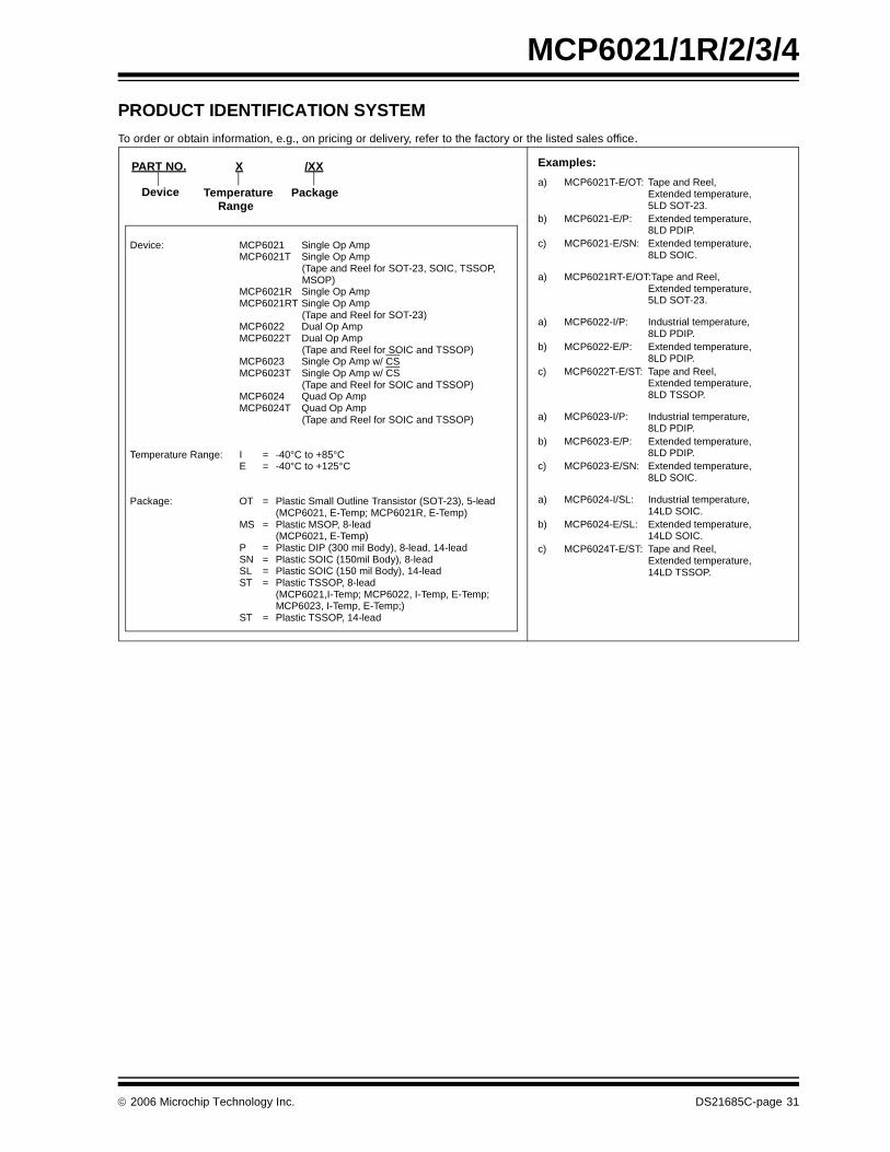
PRODUCT IDENTIFICATION SYSTEM
To order or obtain information, e.g., on pricing or delivery, refer to the factory or the listed sales office.
Device: MCP6021 Single Op AmpMCP6021T Single Op Amp
(Tape and Reel for SOT-23, SOIC, TSSOP, MSOP)
MCP6021R Single Op AmpMCP6021RT Single Op Amp
(Tape and Reel for SOT-23)MCP6022 Dual Op AmpMCP6022T Dual Op Amp
(Tape and Reel for SOIC and TSSOP)MCP6023 Single Op Amp w/ CSMCP6023T Single Op Amp w/ CS
(Tape and Reel for SOIC and TSSOP)MCP6024 Quad Op AmpMCP6024T Quad Op Amp
(Tape and Reel for SOIC and TSSOP)
Temperature Range: I = -40°C to +85°CE = -40°C to +125°C
Package: OT = Plastic Small Outline Transistor (SOT-23), 5-lead(MCP6021, E-Temp; MCP6021R, E-Temp)
MS = Plastic MSOP, 8-lead(MCP6021, E-Temp)
P = Plastic DIP (300 mil Body), 8-lead, 14-leadSN = Plastic SOIC (150mil Body), 8-leadSL = Plastic SOIC (150 mil Body), 14-leadST = Plastic TSSOP, 8-lead
(MCP6021,I-Temp; MCP6022, I-Temp, E-Temp;MCP6023, I-Temp, E-Temp;)
ST = Plastic TSSOP, 14-lead
PART NO. X /XX
PackageTemperatureRange
Device
Examples:
a) MCP6021T-E/OT: Tape and Reel,Extended temperature, 5LD SOT-23.
b) MCP6021-E/P: Extended temperature, 8LD PDIP.
c) MCP6021-E/SN: Extended temperature,8LD SOIC.
a) MCP6021RT-E/OT:Tape and Reel,Extended temperature, 5LD SOT-23.
a) MCP6022-I/P: Industrial temperature,8LD PDIP.
b) MCP6022-E/P: Extended temperature,8LD PDIP.
c) MCP6022T-E/ST: Tape and Reel,Extended temperature,8LD TSSOP.
a) MCP6023-I/P: Industrial temperature, 8LD PDIP.
b) MCP6023-E/P: Extended temperature, 8LD PDIP.
c) MCP6023-E/SN: Extended temperature,8LD SOIC.
a) MCP6024-I/SL: Industrial temperature,14LD SOIC.
b) MCP6024-E/SL: Extended temperature,14LD SOIC.
c) MCP6024T-E/ST: Tape and Reel,Extended temperature,14LD TSSOP.

MCP6021/1R/2/3/4
DS21685C-page 32 © 2006 Microchip Technology Inc.
NOTES:
© 2006 Microchip Technology Inc. DS21685C-page 33
Information contained in this publication regarding deviceapplications and the like is provided only for your convenienceand may be superseded by updates. It is your responsibility toensure that your application meets with your specifications.MICROCHIP MAKES NO REPRESENTATIONS OR WAR-RANTIES OF ANY KIND WHETHER EXPRESS OR IMPLIED,WRITTEN OR ORAL, STATUTORY OR OTHERWISE,RELATED TO THE INFORMATION, INCLUDING BUT NOTLIMITED TO ITS CONDITION, QUALITY, PERFORMANCE,MERCHANTABILITY OR FITNESS FOR PURPOSE.Microchip disclaims all liability arising from this information andits use. Use of Microchip devices in life support and/or safetyapplications is entirely at the buyer’s risk, and the buyer agreesto defend, indemnify and hold harmless Microchip from any andall damages, claims, suits, or expenses resulting from suchuse. No licenses are conveyed, implicitly or otherwise, underany Microchip intellectual property rights.
Trademarks
The Microchip name and logo, the Microchip logo, Accuron, dsPIC, KEELOQ, microID, MPLAB, PIC, PICmicro, PICSTART, PRO MATE, PowerSmart, rfPIC, and SmartShunt are registered trademarks of Microchip Technology Incorporated in the U.S.A. and other countries.
AmpLab, FilterLab, Migratable Memory, MXDEV, MXLAB, PICMASTER, SEEVAL, SmartSensor and The Embedded Control Solutions Company are registered trademarks of Microchip Technology Incorporated in the U.S.A.
Analog-for-the-Digital Age, Application Maestro, dsPICDEM, dsPICDEM.net, dsPICworks, ECAN, ECONOMONITOR, FanSense, FlexROM, fuzzyLAB, In-Circuit Serial Programming, ICSP, ICEPIC, Linear Active Thermistor, MPASM, MPLIB, MPLINK, MPSIM, PICkit, PICDEM, PICDEM.net, PICLAB, PICtail, PowerCal, PowerInfo, PowerMate, PowerTool, Real ICE, rfLAB, rfPICDEM, Select Mode, Smart Serial, SmartTel, Total Endurance, UNI/O, WiperLock and ZENA are trademarks of Microchip Technology Incorporated in the U.S.A. and other countries.
SQTP is a service mark of Microchip Technology Incorporated in the U.S.A.
All other trademarks mentioned herein are property of their respective companies.
© 2006, Microchip Technology Incorporated, Printed in the U.S.A., All Rights Reserved.
Printed on recycled paper.
Note the following details of the code protection feature on Microchip devices:
• Microchip products meet the specification contained in their particular Microchip Data Sheet.
• Microchip believes that its family of products is one of the most secure families of its kind on the market today, when used in the intended manner and under normal conditions.
• There are dishonest and possibly illegal methods used to breach the code protection feature. All of these methods, to our knowledge, require using the Microchip products in a manner outside the operating specifications contained in Microchip’s Data Sheets. Most likely, the person doing so is engaged in theft of intellectual property.
• Microchip is willing to work with the customer who is concerned about the integrity of their code.
• Neither Microchip nor any other semiconductor manufacturer can guarantee the security of their code. Code protection does not mean that we are guaranteeing the product as “unbreakable.”
Code protection is constantly evolving. We at Microchip are committed to continuously improving the code protection features of ourproducts. Attempts to break Microchip’s code protection feature may be a violation of the Digital Millennium Copyright Act. If such actsallow unauthorized access to your software or other copyrighted work, you may have a right to sue for relief under that Act.
Microchip received ISO/TS-16949:2002 quality system certification for its worldwide headquarters, design and wafer fabrication facilities in Chandler and Tempe, Arizona and Mountain View, California in October 2003. The Company’s quality system processes and procedures are for its PICmicro® 8-bit MCUs, KEELOQ® code hopping devices, Serial EEPROMs, microperipherals, nonvolatile memory and analog products. In addition, Microchip’s quality system for the design and manufacture of development systems is ISO 9001:2000 certified.
DS21685C-page 34 © 2006 Microchip Technology Inc.
AMERICASCorporate Office2355 West Chandler Blvd.Chandler, AZ 85224-6199Tel: 480-792-7200 Fax: 480-792-7277Technical Support: http://support.microchip.comWeb Address: www.microchip.com
AtlantaAlpharetta, GA Tel: 770-640-0034 Fax: 770-640-0307
BostonWestborough, MA Tel: 774-760-0087 Fax: 774-760-0088
ChicagoItasca, IL Tel: 630-285-0071 Fax: 630-285-0075
DallasAddison, TX Tel: 972-818-7423 Fax: 972-818-2924
DetroitFarmington Hills, MI Tel: 248-538-2250Fax: 248-538-2260
KokomoKokomo, IN Tel: 765-864-8360Fax: 765-864-8387
Los AngelesMission Viejo, CA Tel: 949-462-9523 Fax: 949-462-9608
San JoseMountain View, CA Tel: 650-215-1444Fax: 650-961-0286
TorontoMississauga, Ontario, CanadaTel: 905-673-0699 Fax: 905-673-6509
ASIA/PACIFICAustralia - SydneyTel: 61-2-9868-6733 Fax: 61-2-9868-6755
China - BeijingTel: 86-10-8528-2100 Fax: 86-10-8528-2104
China - ChengduTel: 86-28-8676-6200 Fax: 86-28-8676-6599
China - FuzhouTel: 86-591-8750-3506 Fax: 86-591-8750-3521
China - Hong Kong SARTel: 852-2401-1200 Fax: 852-2401-3431
China - QingdaoTel: 86-532-8502-7355Fax: 86-532-8502-7205
China - ShanghaiTel: 86-21-5407-5533 Fax: 86-21-5407-5066
China - ShenyangTel: 86-24-2334-2829Fax: 86-24-2334-2393
China - ShenzhenTel: 86-755-8203-2660 Fax: 86-755-8203-1760
China - ShundeTel: 86-757-2839-5507 Fax: 86-757-2839-5571
China - WuhanTel: 86-27-5980-5300Fax: 86-27-5980-5118
China - XianTel: 86-29-8833-7250Fax: 86-29-8833-7256
ASIA/PACIFICIndia - BangaloreTel: 91-80-4182-8400 Fax: 91-80-4182-8422
India - New DelhiTel: 91-11-5160-8631Fax: 91-11-5160-8632
India - PuneTel: 91-20-2566-1512Fax: 91-20-2566-1513
Japan - YokohamaTel: 81-45-471- 6166 Fax: 81-45-471-6122
Korea - GumiTel: 82-54-473-4301Fax: 82-54-473-4302
Korea - SeoulTel: 82-2-554-7200Fax: 82-2-558-5932 or 82-2-558-5934
Malaysia - PenangTel: 60-4-646-8870Fax: 60-4-646-5086
Philippines - ManilaTel: 63-2-634-9065Fax: 63-2-634-9069
SingaporeTel: 65-6334-8870Fax: 65-6334-8850
Taiwan - Hsin ChuTel: 886-3-572-9526Fax: 886-3-572-6459
Taiwan - KaohsiungTel: 886-7-536-4818Fax: 886-7-536-4803
Taiwan - TaipeiTel: 886-2-2500-6610 Fax: 886-2-2508-0102
Thailand - BangkokTel: 66-2-694-1351Fax: 66-2-694-1350
EUROPEAustria - WelsTel: 43-7242-2244-399Fax: 43-7242-2244-393Denmark - CopenhagenTel: 45-4450-2828 Fax: 45-4485-2829
France - ParisTel: 33-1-69-53-63-20 Fax: 33-1-69-30-90-79
Germany - MunichTel: 49-89-627-144-0 Fax: 49-89-627-144-44
Italy - Milan Tel: 39-0331-742611 Fax: 39-0331-466781
Netherlands - DrunenTel: 31-416-690399 Fax: 31-416-690340
Spain - MadridTel: 34-91-708-08-90Fax: 34-91-708-08-91
UK - WokinghamTel: 44-118-921-5869Fax: 44-118-921-5820
WORLDWIDE SALES AND SERVICE
02/16/06