radsaga initial training event 1-6 october 2017, geneva ... · from radiation hardening to brave...
TRANSCRIPT

October 2017
From Radiation HardeningTo BRAVE FPGA devices
RADSAGA Initial Training Event
1-6 October 2017, Geneva
© 2017 Nanoxplore SAS Company ConfidentialCopy not authorized without written approval
Rad Tolerant vs Rad Hardened
Radiation Hardened material is immune to the effects of the radiationand has a higher life cycle. The devices are specifically designed in a control environment and the property is unique.Moreover, Radiation Hardened material are used on devices which are meant to work in high radiation prone areas such as space.
Radiation Tolerant material is a property of the device to be bear radiation till certain limit the material will need replacement afterwards. The devices are designed without compromising other properties of the device.The radiation property could be find in a lot of devices and does not need a specialized controlled environment to make it.Most of these materials usually don't see their use in their lifespan as they are meant to work in normal environment, they are generally used in Cell Phones, Computers, Consumer Electronics, Radiation suits and so on.
Source: https://www.quora.com/What-is-the-difference-between-radiation-hardened-and-radiation-tolerant-components-used-in-space-industry
© 2017 Nanoxplore SAS Company ConfidentialCopy not authorized without written approval
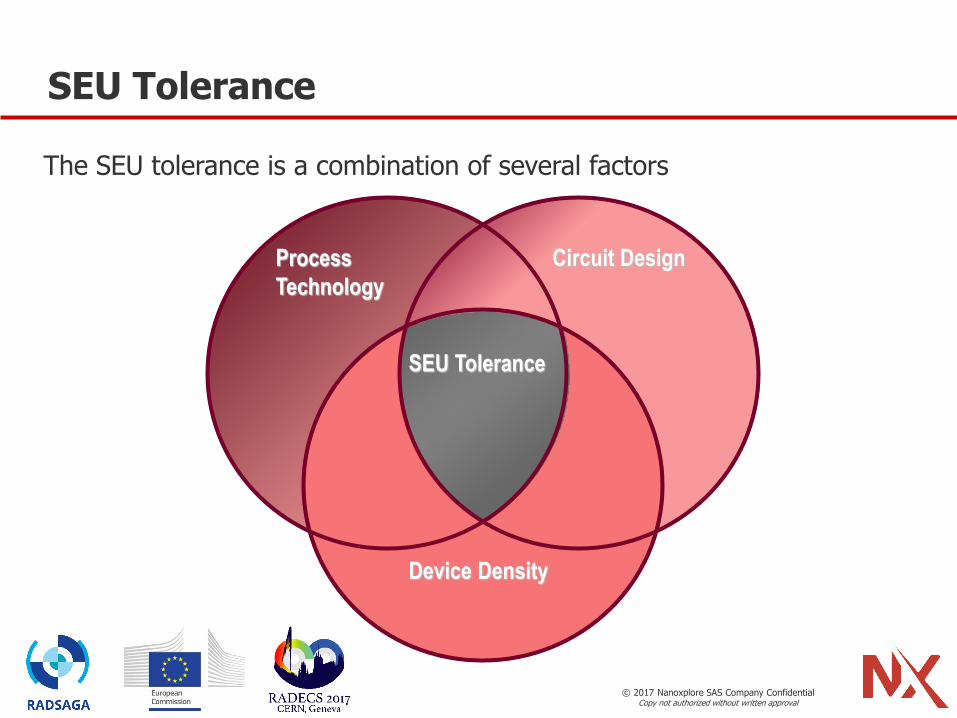
SEU Tolerance
Process
Technology
Circuit Design
Device Density
SEU Tolerance
The SEU tolerance is a combination of several factors
© 2017 Nanoxplore SAS Company ConfidentialCopy not authorized without written approval
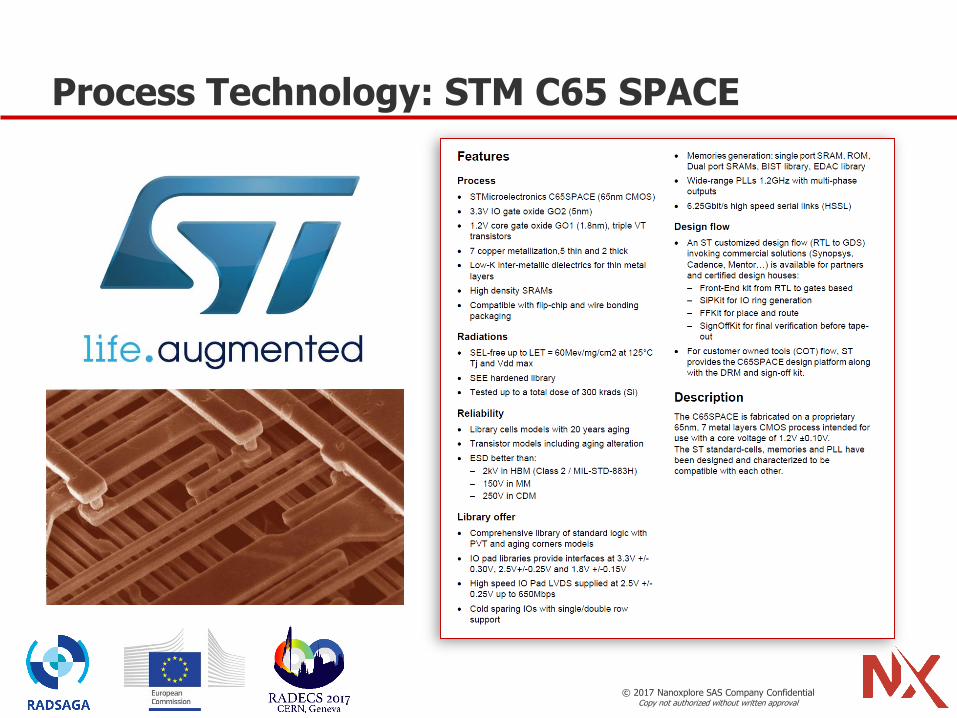
Process Technology: STM C65 SPACE

© 2017 Nanoxplore SAS Company ConfidentialCopy not authorized without written approval
Circuit Design: STM RH65nm Skyrob library
© 2017 Nanoxplore SAS Company ConfidentialCopy not authorized without written approval
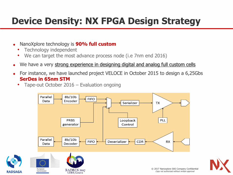
Device Density: NX FPGA Design Strategy
NanoXplore technology is 90% full custom• Technology independent• We can target the most advance process node (i.e 7nm end 2016)
We have a very strong experience in designing digital and analog full custom cells
For instance, we have launched project VELOCE in October 2015 to design a 6,25Gbs SerDes in 65nm STM• Tape-out October 2016 – Evaluation ongoing

© 2017 Nanoxplore SAS Company ConfidentialCopy not authorized without written approval
FPGA
STM 65nm process
Medium complexity• 35K LUT4 & DFF• 2,8Mb RAM• 112 DSP blocks• SpW link interface (1 CODEC, 16 PHY)
• 16 DDR/2/3 PHY• Up to 374 User I/Os
Radiation Performances• TID > 300krads(Si)• SEL immune• SER: § further slides

© 2017 Nanoxplore SAS Company ConfidentialCopy not authorized without written approval
NX FPGAs are Rad Hardened
All logic of NX FPGAs is hardened by design (RHBD) and simulated with TFIT software
On top of it, Embedded Configuration Memory Integrity Check (“CMIC”)
•Clock Tree
Clock bufferMatrix system
• Other Logic Cells(SKYROB)
• Cfg Memory
• User Register
• DFF
• Register File
• DPRAM
EDAC DICE
DMRTMR

© 2017 Nanoxplore SAS Company ConfidentialCopy not authorized without written approval
DICE cell
DICE selected
5 well-knowns solutions:• DICE cell (12T)• HIT cell (12T)• LIU cell (15T)• ROCKET cell (16T)• WHITAKER cell (16T)
Choice of DICE *
The SEU Hardened Memory point can only change value if 2 channels switch at the same time An ion impact on a single channel cannot flip the memory.
Regarding Radiation Hardened Memory Cells & DFF, all solutions go against the level of integration, since we add transistors.
* DICE stands for Dual Interlocked storage CEll
© 2017 Nanoxplore SAS Company ConfidentialCopy not authorized without written approval
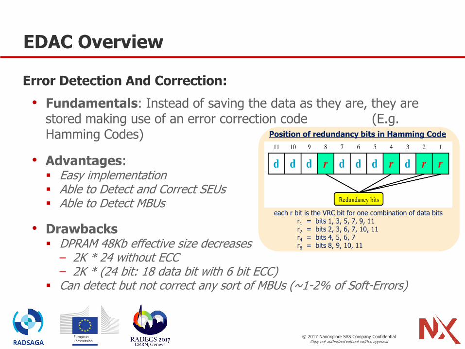
EDAC Overview
Error Detection And Correction:
• Fundamentals: Instead of saving the data as they are, they are stored making use of an error correction code (E.g. Hamming Codes)
• Advantages: Easy implementation Able to Detect and Correct SEUs Able to Detect MBUs
• Drawbacks DPRAM 48Kb effective size decreases
– 2K * 24 without ECC– 2K * (24 bit: 18 data bit with 6 bit ECC)
Can detect but not correct any sort of MBUs (~1-2% of Soft-Errors)
Position of redundancy bits in Hamming Code
each r bit is the VRC bit for one combination of data bitsr1 = bits 1, 3, 5, 7, 9, 11r2 = bits 2, 3, 6, 7, 10, 11r4 = bits 4, 5, 6, 7r8 = bits 8, 9, 10, 11

© 2017 Nanoxplore SAS Company ConfidentialCopy not authorized without written approval
CMIC Overview
CMIC= Configuration Memory Integrity (= Scrubber Ctrl)• The CMIC is an embedded engine performing automatic verification and repair of the
configuration memory. • A CMIC reference memory is initialized during the bit stream download process with reference
data computed by the NanoXmap software. • Once the initialization is done, the CMIC engine can be periodically activated to perform the
following sequence: 1. Read configuration data 2. Calculate signature 3. Compare the signature with CMIC reference 4. If a mismatch is detected:
– a. Calculate faulty address (BAD @) and faulty bit location– b. Read DATA[BAD @] – c. Repair flipped bit – d. Write DATA[BAD @]
• The CMIC period can be set by the user. The minimum period is 5.3 ms and the maximum 65 days. The configuration memory scan takes 4ms.
• The CMIC reference memory is protected by ECC. • The CMIC does not need to access the external NVRAM when performing checks and repairs at
run time.
BIT
STREAM
+
CMIC
ECC
NVRAMCONFIGURATION
MEMORY
CMIC REF
MEMORY
(ECC PROTECTED)
NG-MEDIUM
BIT STREAM
CM
IC R
EF

© 2017 Nanoxplore SAS Company ConfidentialCopy not authorized without written approval
Radiations Results

© 2017 Nanoxplore SAS Company ConfidentialCopy not authorized without written approval
2 SEE campaigns done in Q4CY16
• 1st silicon used, out of wfab in Summer-16,
• Packaged in LGA625 tested,
• First radiative test done in October 2016: memory configuration test done – SER / day device level 1.96e-4
• Second radiative test campaign done end of November 2016: DFF static and dynamic test, CMIC and DPRAM
SEE campaign

© 2017 Nanoxplore SAS Company ConfidentialCopy not authorized without written approval
SEE campaign
Ion Beam cocktail used (High penetration ions):
http://www.cyc.ucl.ac.be/HIF/HIF.phpMore information:

© 2017 Nanoxplore SAS Company ConfidentialCopy not authorized without written approval
Radiations: SEU / SET Tests Overview
Temperature measured 19->34°C
Supply at their min value (-10%):
VDD1V2 Core supply 1.08V• No voltage sensor->1.045V inside the chip.
Angular cross-section for config given in chip plan
Normal incidence for other tests
Fluence over 106 p/cm² for config, static DFF, dynamic DFF
Test Devices under test
Config SEU 6 138 096 configuration memory
DPRAM SEU 56 DPRAM with EDAC ST_DPHD_2048x24m4_b = 2 752 512 bit
DFF static 32 256 DFF
1008 matrix system output of the clock tree

© 2017 Nanoxplore SAS Company ConfidentialCopy not authorized without written approval
Radiations: SEU / SET Tests Results
Orbital Upset Rate calculation (CREME 96 model):• GEO• solar min• shielding = 100mils• sensitive volume thickness = 2µm• Unhardened SRAM SER /9400
Weilbull parameter chip6+7
SIGsat (cm2/bit) 5.1852E-09
L0 (MeV/(mg/cm²)) 0.11214
W (MeV) 36.4286
s 4.44737
Configuration Memory SEU@ 30°C,1.045V
SER
SEU/config/day 2.7E-11 SEU/config/day
SEU/chip/day 1.7E-04 SEU/chip/day
SEU/chip/year 6.1E-02 SEU/chip/year SER 16,4years
Chess-board pattern
SER normal incidence

© 2017 Nanoxplore SAS Company ConfidentialCopy not authorized without written approval
Radiations: Config SEU
1E-15
1E-14
1E-13
1E-12
1E-11
1E-10
1E-09
1E-08
0.0 10.0 20.0 30.0 40.0 50.0 60.0 70.0 80.0 90.0 100.0
SE
U C
ross-s
ecti
on
(cm
²/b
it)
LET Eff (MeV/(mg/cm²))
SEU config cross-section(LET) of chip6&7
SEU DUT#6
SEU DUT#6 Weilbull
SEU DUT#6 'tilted phi=90
SEU DUT#6 tilted phi=0
SEU DUT#7
SEU DUT#7 Weilbull"
SEU DUT#7 'tilted phi=0'

© 2017 Nanoxplore SAS Company ConfidentialCopy not authorized without written approval
Radiations: Static DFF SEU, clock SET
1.00E-15
1.00E-14
1.00E-13
1.00E-12
1.00E-11
1.00E-10
1.00E-09
1.00E-08
1.00E-07
0.0 10.0 20.0 30.0 40.0 50.0 60.0 70.0 80.0 90.0 100.0
SE
U C
ross-s
ecti
on
(cm
²/cell)
LET Eff (MeV/(mg/cm²))
DFF SEU & Clock SET cross-section(LET)
SEU config BRAVE#6
SEU config BRAVE#6 Weilbull
SEU dff per config BRAVE#6
SET clock per config BRAVE#6
SET Xs 2 decadeunder config XS
DFF SEU Xs 3 decadeunder config XS
© 2017 Nanoxplore SAS Company ConfidentialCopy not authorized without written approval
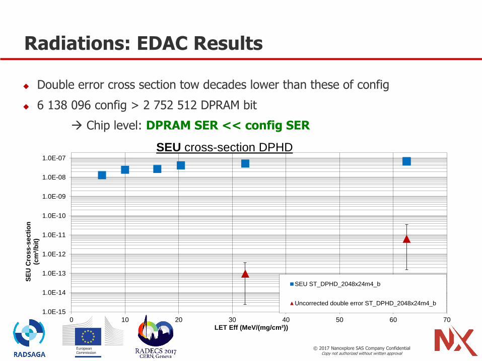
Radiations: EDAC Results
Double error cross section tow decades lower than these of config
6 138 096 config > 2 752 512 DPRAM bit
Chip level: DPRAM SER << config SER
1.0E-15
1.0E-14
1.0E-13
1.0E-12
1.0E-11
1.0E-10
1.0E-09
1.0E-08
1.0E-07
0 10 20 30 40 50 60 70
SE
U C
ross-s
ecti
on
(cm
²/b
it)
LET Eff (MeV/(mg/cm²))
SEU cross-section DPHD
SEU ST_DPHD_2048x24m4_b
Uncorrected double error ST_DPHD_2048x24m4_b

© 2017 Nanoxplore SAS Company ConfidentialCopy not authorized without written approval
Radiations: CMIC Results
No double error recorded in the EDAC reference memory ST_SPREG_144x27m4
1.00E-15
1.00E-14
1.00E-13
1.00E-12
1.00E-11
1.00E-10
1.00E-09
1.00E-08
0 10 20 30 40 50 60 70 80 90 100
SE
U C
ross-s
ecti
on
(cm
²/b
it)
LET Eff (MeV/(mg/cm²))
SEU config cross-section(LET) with CMIC
SEU config BRAVE#6 with CMIC
SEU config BRAVE#6 without CMIC
SEU config double error in same signature BRAVE#6
>1 decade

© 2017 Nanoxplore SAS Company ConfidentialCopy not authorized without written approval
Radiations: Dynamic DFF test
• DFF dynamic with no Reset
DFFINV(LUT)32
Clk
Section
x1008
32
Mtx_sysClock tree

© 2017 Nanoxplore SAS Company ConfidentialCopy not authorized without written approval
Radiations: Dynamic DFF test
1E-15
1E-14
1E-13
1E-12
1E-11
1E-10
1E-09
1E-08
0.0000001
0 10 20 30 40 50 60 70 80 90 100
SE
U C
ross
-secti
on
(cm
²/cell)
LET Eff (MeV/(mg/cm²))
toggle dff error cross-section(LET)
error toggle dff per config bit BRAVE#6
SEU config BRAVE#6
SEU config BRAVE#6 Weilbull
Toggle dff cross-section contribution to chip cross-section negligible regarding to the config cross section

© 2017 Nanoxplore SAS Company ConfidentialCopy not authorized without written approval
Radiations: SEFI
• SEFI Config or context can not be read/written (mapped application status unknown)
1.00E-15
1.00E-14
1.00E-13
1.00E-12
1.00E-11
1.00E-10
1.00E-09
1.00E-08
1.00E-07
0.0 10.0 20.0 30.0 40.0 50.0 60.0 70.0 80.0 90.0 100.0
SE
U C
ross-s
ecti
on
(cm
²/ch
ip)
LET Eff (MeV/(mg/cm²))
SEFI cross-section(LET)
SEU config BRAVE#6
SEU config BRAVE#6 Weilbull
SEFI flux per config
Overestimation of SEFI cross-section flux UCL >> Space flux
Day 2 bitstream reading sequence modified

© 2017 Nanoxplore SAS Company ConfidentialCopy not authorized without written approval
Next SEE Campaigns
Heavy Ions campaign on 2nd run NG-Medium, on behalf of VEGAS contract, at UCL HIF
Protons campaign, done by ESA at PSI
New Radiation campaign, expected from CERN at PSI & CHARM
New Radiation campaign, expected from Brasilian partner• TID (60CO & X-Rays)• Heavy Ions• Protons• Neutrons
SEP17ccccccccccccccccccc
NOV17
TBD c& VVVVVV
T0= SEP17?• T0+4mths• T0+3mths• T0+3mths• T0+3mths

© 2017 Nanoxplore SAS Company ConfidentialCopy not authorized without written approval
NanoXplore Rad-Hard FPGA Roadmap
Design validated
NanoXmap available
DevKit available
Proto available
Space Qual Q2CY18
Design in-progress
Tape-out End17
NanoXmapQ1CY18
1st Proto Q3CY18
DevKit Q3CY18
1st Test Chip May18
Tape-out Q2CY19
NanoXmapQ2CY19
1st Proto Q4CY19
DevKit Q4CY19
NX has successfully delivered the NG-MEDIUM on time and doesn’t expect any delay on NG-LARGE and NG-ULTRA schedule
2017 2018 2019

© 2017 Nanoxplore SAS Company ConfidentialCopy not authorized without written approval
Questions & AnswersThank you

© 2017 Nanoxplore SAS Company Confidential
www.nanoxplore.comwww.NanoXplore.com

© 2017 Nanoxplore SAS Company ConfidentialCopy not authorized without written approval
Questionnaire
Q1. What are 3 factors which have impact of SEU performances?• Answer: The 3 factors are Process Technology Circuit design Device density.
Q2. Which are NX design solutions used to harden their FPGA devices?• Answer: NX has used 4 different design approaches to harden FPGA devices: Selection of DICE as a RHBD memory latch Use of ECC for RAM blocks Duplication of Clock tree Extract of IP block from a European 65nm ASIC library.Even on top of that, NX has embed a Scrubber Controller which verifies the integrity of the bitstream, 24h a day, 7days a week and 365days a year.
Q3. What is the main interest of Weibull parameters?• Answer: Weibull parameters allows the user to comput the orbital upset rate for a
dedicated Space mission, such as LEO/EOS or GEO/SatCom.