radeon sea islands 3d/compute register reference...
TRANSCRIPT

Revision 1.0 September 19, 2012
© 2012 Advanced Micro Devices, Inc. Proprietary 1
Radeon Sea Islands 3D/Compute Register
Reference Guide

Revision 1.0 September 19, 2012
© 2012 Advanced Micro Devices, Inc. Proprietary 2
Trademarks AMD, the AMD Arrow logo, Athlon, and combinations thereof, ATI, ATI logo, Radeon, and Crossfire are trademarks of Advanced Micro Devices, Inc. Microsoft and Windows are registered trademarks of Microsoft Corporation. Other product names used in this publication are for identification purposes only and may be trademarks of their respective companies. Disclaimer The contents of this document are provided in connection with Advanced Micro Devices, Inc. ("AMD") products. AMD makes no representations or warranties with respect to the accuracy or completeness of the contents of this publication and reserves the right to make changes to specifications and product descriptions at any time without notice. No license, whether express, implied, arising by estoppel, or otherwise, to any intellectual property rights are granted by this publication. Except as set forth in AMD's Standard Terms and Conditions of Sale, AMD assumes no liability whatsoever, and disclaims any express or implied warranty, relating to its products including, but not limited to, the implied warranty of merchantability, fitness for a particular purpose, or infringement of any intellectual property right. AMD's products are not designed, intended, authorized or warranted for use as components in systems intended for surgical implant into the body, or in other applications intended to support or sustain life, or in any other application in which the failure of AMD's product could create a situation where personal injury, death, or severe property or environmental damage may occur. AMD reserves the right to discontinue or make changes to its products at any time without notice. © 2012 Advanced Micro Devices, Inc. All rights reserved.

Revision 1.0 September 19, 2012
© 2012 Advanced Micro Devices, Inc. Proprietary 3
1. VERTEX GROUPER AND TESSELLATOR REGISTERS .......................................................................................... 4
2. PRIMITIVE ASSEMBLY REGISTERS ................................................................................................................ 39
3. GENERAL SHADER REGISTERS ...................................................................................................................... 68
4. SHADER INSTRUCTIONS ............................................................................................................................... 69
5. SHADER BUFFER RESOURCE DESCRIPTOR .................................................................................................. 160
6. SHADER IMAGE RESOURCE DESCRIPTOR ................................................................................................... 163
7. SHADER IMAGE RESOURCE SAMPLER DESCRIPTOR ................................................................................... 167
8. FLAT SCRATCH DESCRIPTOR ...................................................................................................................... 170
9. SPI SHADER REGISTERS .............................................................................................................................. 171
10. SPI REGISTERS ....................................................................................................................................... 188
11. COMPUTE REGISTERS ............................................................................................................................ 196
12. TILING REGISTERS .................................................................................................................................. 201
13. SURFACE SYNCHRONIZATION REGISTERS .............................................................................................. 203
14. TEXTURE PIPE REGISTERS ...................................................................................................................... 206
15. DEPTH BUFFER REGISTERS ..................................................................................................................... 207
16. COLOR BUFFER REGISTERS .................................................................................................................... 226

Revision 1.0 September 19, 2012
© 2012 Advanced Micro Devices, Inc. Proprietary 4
1. Vertex Grouper and Tessellator Registers
VGT:IA_CNTL_STATUS · [R] · 32 bits · Access: 32 · GpuF0MMReg:0x88dc
DESCRIPTION: Status Bits
Field Name Bits Default Description
IA_BUSY 0 none If set, the IA is busy
IA_DMA_BUSY 1 none If set, the DMA block within the IA is busy
IA_DMA_REQ_BUSY 2 none If set, the DMA request within the IA is busy
IA_GRP_BUSY 3 none If set, the Grouper block within the IA is busy
IA_ADC_BUSY 4 none If set, the ADC block within the IA is busy
VGT:IA_ENHANCE · [R/W] · 32 bits · Access: 32 · GpuF0MMReg:0x28a70
DESCRIPTION: Used for Late Additions of Control Bits.
Field Name Bits Default Description
MISC 31:0 none Misc bit
VGT:IA_MULTI_VGT_PARAM · [R/W] · 32 bits · Access: 32 · GpuF0MMReg:0x28aa8
DESCRIPTION: Specifies information for multiple VGT configurations
Field Name Bits Default Description
PRIMGROUP_SIZE 15:0 0xFF Number of primitives sent to one VGT block before
switching to the next VGT block. It has an implied +1 (0
= 1 prim/group; 255 = 256 prims/group). Setting bigger
than 255 will cause performance degradation. For
PATCH primitives, this should be set no bigger than (
(256/# of input control points) - 1 ). For dx11
tessellation, this should be set to a multiple of the
number of patches per threadgroup. If this value is
programmed to 0 (1 prim/group) it is internally treated as
1 (2 prims/group)
If PARTIAL_ES_WAVE_ON is OFF and streamout is
enabled, the primgroup size must be less than 256 for 2
SE designs. For Adjacent primtypes, it should be less
than 128.
In Major Mode 1, the primgroup_size programming
cannot exceed 63
PARTIAL_VS_WAVE_ON 16 0x0 If this bit is set, then the VGT will issue a vswave as
soon as a primgroup is finished. Otherwise, the VGT will
continue a vswave from one primgroup to next

Revision 1.0 September 19, 2012
© 2012 Advanced Micro Devices, Inc. Proprietary 5
primgroup within a draw call. This must be enabled if
streamout is enabled
POSSIBLE VALUES:
00 - partial_vs_wave_off
01 - partial_vs_wave_on
SWITCH_ON_EOP 17 0x0 If this bit is set, the IA will switch between VGT blocks
at packet boundaries, otherwise it will switch based on
primgroups which are created according to the
programming of PRIMGROUP_SIZE. Must be set to 1 if
using Major Mode 1 without Tess, i.e. Passthru etc.
POSSIBLE VALUES:
00 - switch_on_primgroup_size
01 - switch_on_eop
PARTIAL_ES_WAVE_ON 18 0x0 If this bit is set, then the VGT will issue a eswave as
soon as a primgroup is finished. Otherwise, the VGT will
continue a eswave from one primgroup to next
primgroup within a draw call.
POSSIBLE VALUES:
00 - partial_es_wave_off
01 - partial_es_wave_on
SWITCH_ON_EOI 19 0x0 If this bit is set, the IA will switch between VGT blocks
at end of instance boundaries, otherwise it will switch
based on primgroups which are created according to the
programming of PRIMGROUP_SIZE. Must be set to 1 if
using Dx11 with tessellation and prim_id needs to be
correct. If this is set, PARTIAL_ES_WAVE_ON must
be set because the GS table logic doesn`t allow multiple
prim groups to share a GS wave.
POSSIBLE VALUES:
00 - switch_on_primgroup_size
01 - switch_on_eoi
WD_SWITCH_ON_EOP 20 0x0 If this bit is set, the WD will switch between IA blocks at
packet boundaries, otherwise it will switch based on
workgroupgroups which are created according to the
programming of (2 * PRIMGROUP_SIZE). Must be set
to 1 if using Major Mode 1 without Tess, i.e. Passthru
etc. Must also be set to 1 if RESET INDICES are
enabled, or when certain primitive types are used :
DI_PT_POLYGON, DI_PT_LINELOOP,
DI_PT_TRIFAN, DI_PT_TRISTRIP_ADJ
POSSIBLE VALUES:
00 - switch_on_workgroup_size
01 - switch_on_eop
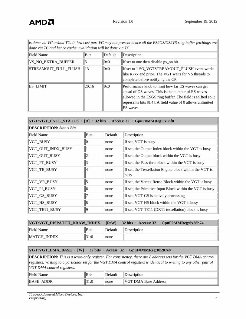
VGT:VGT_CACHE_INVALIDATION · [R/W] · 32 bits · Access: 32 · GpuF0MMReg:0x88c4
DESCRIPTION: This register is used in specifying whether cache invalidation of ES2GS and GS2VS ring buffers
Revision 1.0 September 19, 2012
© 2012 Advanced Micro Devices, Inc. Proprietary 6
is done via VC or/and TC. In low cost part VC may not present hence all the ES2GS/GS2VS ring buffer fetchings are
done via TC and hence cache invalidation will be done via TC.
Field Name Bits Default Description
VS_NO_EXTRA_BUFFER 5 0x0 If set to one then disable gs_on bit
STREAMOUT_FULL_FLUSH 13 0x0 If set to 1 SO_VGTSTREAMOUT_FLUSH event works
like R7xx and prior. The VGT waits for VS threads to
complete before notifying the CP.
ES_LIMIT 20:16 0x0 Performance knob to limit how far ES waves can get
ahead of GS waves. This is the number of ES waves
allowed in the ESGS ring buffer. The field is shifted so it
represents bits [8:4]. A field value of 0 allows unlimited
ES waves.
VGT:VGT_CNTL_STATUS · [R] · 32 bits · Access: 32 · GpuF0MMReg:0x88f0
DESCRIPTION: Status Bits
Field Name Bits Default Description
VGT_BUSY 0 none If set, VGT is busy
VGT_OUT_INDX_BUSY 1 none If set, the Output Index block within the VGT is busy
VGT_OUT_BUSY 2 none If set, the Output block within the VGT is busy
VGT_PT_BUSY 3 none If set, the Pass-thru block within the VGT is busy
VGT_TE_BUSY 4 none If set, the Tessellation Engine block within the VGT is
busy
VGT_VR_BUSY 5 none If set, the Vertex Reuse Block within the VGT is busy
VGT_PI_BUSY 6 none If set, the Primitive Input Block within the VGT is busy
VGT_GS_BUSY 7 none If set, VGT GS is actively processing
VGT_HS_BUSY 8 none If set, VGT HS block within the VGT is busy
VGT_TE11_BUSY 9 none If set, VGT TE11 (DX11 tessellation) block is busy
VGT:VGT_DISPATCH_DRAW_INDEX · [R/W] · 32 bits · Access: 32 · GpuF0MMReg:0x28b74
Field Name Bits Default Description
MATCH_INDEX 31:0 none
VGT:VGT_DMA_BASE · [W] · 32 bits · Access: 32 · GpuF0MMReg:0x287e8
DESCRIPTION: This is a write-only register. For consistency, there are 8 address sets for the VGT DMA control
registers. Writing to a particular set for the VGT DMA control registers is identical to writing to any other pair of
VGT DMA control registers.
Field Name Bits Default Description
BASE_ADDR 31:0 none VGT DMA Base Address

Revision 1.0 September 19, 2012
© 2012 Advanced Micro Devices, Inc. Proprietary 7
This address must be naturally aligned to a 16-bit word.
Therefore, bit 0 of this register must be 0
VGT:VGT_DMA_BASE_HI · [W] · 32 bits · Access: 32 · GpuF0MMReg:0x287e4
DESCRIPTION: This is a write-only register. For consistency, there are 8 address sets for the VGT DMA control
registers. Writing to a particular set for the VGT DMA control registers is identical to writing to any other pair of
VGT DMA control registers. It contains the upper 8 bits of the DMA base address
Field Name Bits Default Description
BASE_ADDR 7:0 none This specifies upper 8-bits of 40-bits of DMA address
VGT:VGT_DMA_INDEX_TYPE · [W] · 32 bits · Access: 32 · GpuF0MMReg:0x28a7c
DESCRIPTION: This is a write-only register. For consistency, there are 8 address sets for the VGT DMA control
registers. Writing to a particular set for the VGT DMA control registers is identical to writing to any other pair of
VGT DMA control registers
Field Name Bits Default Description
INDEX_TYPE 1:0 none VGT DMA Index Type
POSSIBLE VALUES:
00 - VGT_INDEX_16: VGT_INDEX_16 16-bit
index
01 - VGT_INDEX_32: VGT_INDEX_32 32-bit
index
SWAP_MODE 3:2 none DMA Swap mode
POSSIBLE VALUES:
00 - VGT_DMA_SWAP_NONE:
VGT_DMA_SWAP_NONE No swap
01 - VGT_DMA_SWAP_16_BIT:
VGT_DMA_SWAP_16_BIT 16-bit swap
0xAABBCCDD -> 0xBBAADDCC
02 - VGT_DMA_SWAP_32_BIT:
VGT_DMA_SWAP_32_BIT 32-bit swap
0xAABBCCDD -> 0xDDCCBBAA
03 - VGT_DMA_SWAP_WORD:
VGT_DMA_SWAP_WORD word swap
0xAABBCCDD -> 0xCCDDAABB
BUF_TYPE 5:4 none Used to specify DMA buffer type
POSSIBLE VALUES:
00 - VGT_DMA_BUF_MEM: VGT DMA index
buffer in memory (normal DMA request)
01 - VGT_DMA_BUF_RING: VGT DMA index
buffer in a ring
02 - VGT_DMA_BUF_SETUP: VGT DMA index
buffer ring setup transfer
RDREQ_POLICY 7:6 none Used to specify the L2 policy for fetches
POSSIBLE VALUES:
00 - VGT_POLICY_LRU: LRU
01 - VGT_POLICY_STREAM: STREAM

Revision 1.0 September 19, 2012
© 2012 Advanced Micro Devices, Inc. Proprietary 8
02 - VGT_POLICY_BYPASS: BYPASS
ATC 8 none Used to specify the ATC for fetches
NOT_EOP 9 none Used to specify whether this DMA fetch is the last fetch
of a draw call. When using dispatch draw, the entire
draw is broken into sub draws and sub dma calls could
be seen with not_eop set.
POSSIBLE VALUES:
00 - normal eop
01 - suppress eop
REQ_PATH 10 none POSSIBLE VALUES:
00 - MC Hub
01 - TCI Interface
VGT:VGT_DMA_MAX_SIZE · [W] · 32 bits · Access: 32 · GpuF0MMReg:0x28a78
DESCRIPTION: This is a write-only register. This register is used for handling index out of bound issue. It is
expected that driver set this register to less than or equal to VGT_DMA_SIZE, specifying how many actual good
data to be read from index buffer. If VGT_MAX_SIZE < VGT_DMA_SIZE, the reset of fetched indices are set to
zero in VGT
Field Name Bits Default Description
MAX_SIZE 31:0 none VGT DMA maximum number of indices until out of
bound index buffer is accessed
VGT:VGT_DMA_NUM_INSTANCES · [W] · 32 bits · Access: 32 · GpuF0MMReg:0x28a88
DESCRIPTION: This register specifies the number of instances value specified in the draw call. If instances are
off, then this register is set to zero or one. For consistency, there are 8 address sets for the VGT DMA control
registers. Writing to a particular set for the VGT DMA control registers is identical to writing to any other pair of
VGT DMA control registers.
Field Name Bits Default Description
NUM_INSTANCES 31:0 none VGT DMA Number of Instances, minimum value is 1
VGT:VGT_DMA_SIZE · [W] · 32 bits · Access: 32 · GpuF0MMReg:0x28a74
DESCRIPTION: This is a write-only register. For consistency, there are 8 address sets for the VGT DMA control
registers. Writing to a particular set for the VGT DMA control registers is identical to writing to any other pair of
VGT DMA control registers
Field Name Bits Default Description
NUM_INDICES 31:0 none VGT DMA Number of indices
VGT:VGT_DRAW_INITIATOR · [W] · 32 bits · Access: 32 · GpuF0MMReg:0x287f0
DESCRIPTION: Ring-specific: This is a write-only register.
VGT_DRAW_INITIATOR is the register for triggering execution of a draw packet (2D or 3D).
The act of writing this register is a trigger that initiates processing in the VGT.

Revision 1.0 September 19, 2012
© 2012 Advanced Micro Devices, Inc. Proprietary 9
Field Name Bits Default Description
SOURCE_SELECT 1:0 none Input Source Select.
If the Source Select field is set to `Auto-increment Index`
mode and the Primitive Type is set to `Tri List w/Flags`,
then the draw initiator is processed as just a regular `Tri
List`.
POSSIBLE VALUES:
00 - DI_SRC_SEL_DMA: VGT DMA Data
02 - DI_SRC_SEL_AUTO_INDEX: Auto-increment
Index
MAJOR_MODE 3:2 none Major Mode
POSSIBLE VALUES:
00 - DI_MAJOR_MODE_0: DI_MAJOR_MODE_0
Normal (Implicit) Mode -- applies only to prim types 0-
21. Some VGT state registers are ignored (their values
implied) in this mode.
01 - DI_MAJOR_MODE_1: DI_MAJOR_MODE_1
Explicit Mode -- Configuration completely specified by
state registers.
NOT_EOP 5 none This bit indicates that this draw initiator should not
generate an end-of-packet signal because it will be
followed by one or more chained draw initiators. Care
must be taken so that this draw initiator is immediately
followed, at the hardware interface, by a chained draw
initiator. (In other words, chained draw initiators cannot
be separated over driver buffer boundaries that can be
interrupted. This bit is primarily intended to be set by the
CP to improve the processing parallelism of small 2D
blits.)
POSSIBLE VALUES:
00 - normal eop
01 - suppress eop
USE_OPAQUE 6 none This bit indicates that this draw call is a opaque draw call
POSSIBLE VALUES:
00 - non-opaque draw
01 - opaque draw
VGT:VGT_ENHANCE · [R/W] · 32 bits · Access: 32 · GpuF0MMReg:0x28a50
DESCRIPTION: Used for Late Additions of Control Bits.
Field Name Bits Default Description
MISC 31:0 none Misc bit
VGT:VGT_ESGS_RING_ITEMSIZE · [R/W] · 32 bits · Access: 32 · GpuF0MMReg:0x28aac
DESCRIPTION: Size of each vertex written to the ESGS Ring bufer
Field Name Bits Default Description
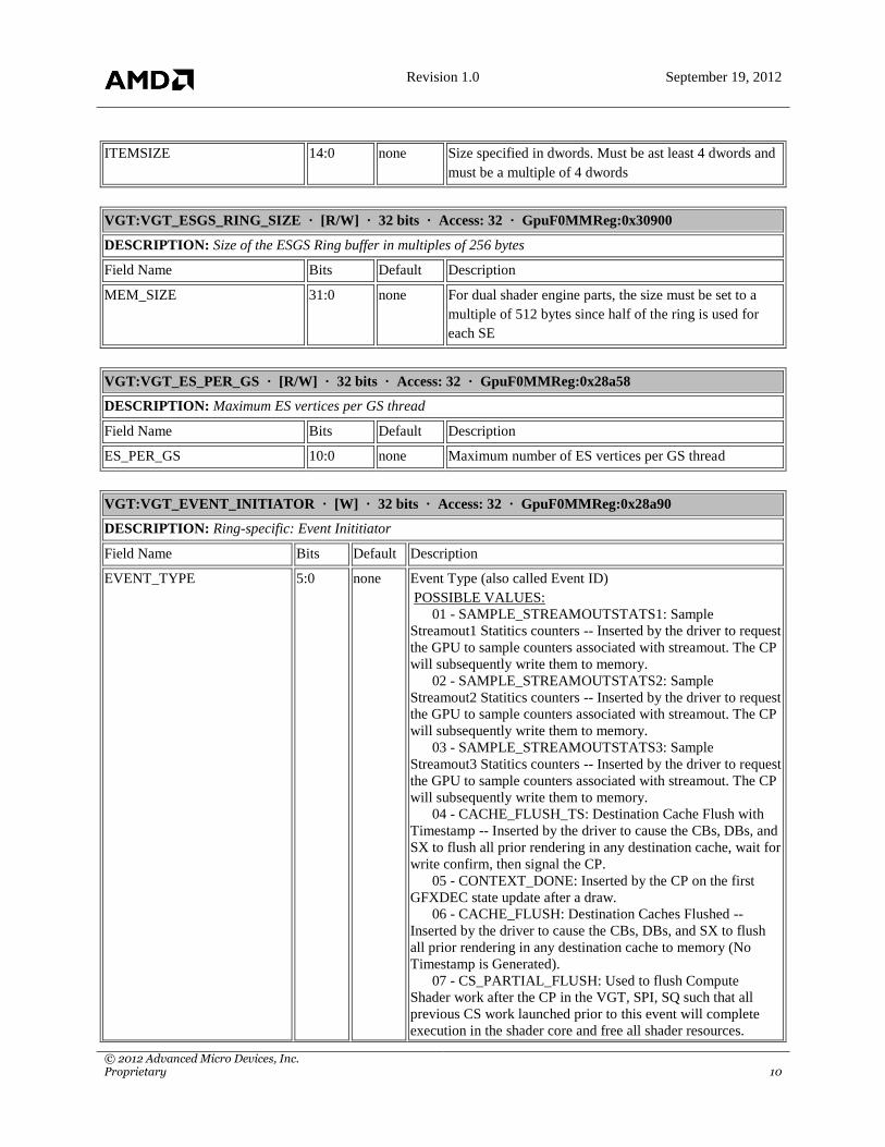
Revision 1.0 September 19, 2012
© 2012 Advanced Micro Devices, Inc. Proprietary 10
ITEMSIZE 14:0 none Size specified in dwords. Must be ast least 4 dwords and
must be a multiple of 4 dwords
VGT:VGT_ESGS_RING_SIZE · [R/W] · 32 bits · Access: 32 · GpuF0MMReg:0x30900
DESCRIPTION: Size of the ESGS Ring buffer in multiples of 256 bytes
Field Name Bits Default Description
MEM_SIZE 31:0 none For dual shader engine parts, the size must be set to a
multiple of 512 bytes since half of the ring is used for
each SE
VGT:VGT_ES_PER_GS · [R/W] · 32 bits · Access: 32 · GpuF0MMReg:0x28a58
DESCRIPTION: Maximum ES vertices per GS thread
Field Name Bits Default Description
ES_PER_GS 10:0 none Maximum number of ES vertices per GS thread
VGT:VGT_EVENT_INITIATOR · [W] · 32 bits · Access: 32 · GpuF0MMReg:0x28a90
DESCRIPTION: Ring-specific: Event Inititiator
Field Name Bits Default Description
EVENT_TYPE 5:0 none Event Type (also called Event ID)
POSSIBLE VALUES:
01 - SAMPLE_STREAMOUTSTATS1: Sample
Streamout1 Statitics counters -- Inserted by the driver to request
the GPU to sample counters associated with streamout. The CP
will subsequently write them to memory.
02 - SAMPLE_STREAMOUTSTATS2: Sample
Streamout2 Statitics counters -- Inserted by the driver to request
the GPU to sample counters associated with streamout. The CP
will subsequently write them to memory.
03 - SAMPLE_STREAMOUTSTATS3: Sample
Streamout3 Statitics counters -- Inserted by the driver to request
the GPU to sample counters associated with streamout. The CP
will subsequently write them to memory.
04 - CACHE_FLUSH_TS: Destination Cache Flush with
Timestamp -- Inserted by the driver to cause the CBs, DBs, and
SX to flush all prior rendering in any destination cache, wait for
write confirm, then signal the CP.
05 - CONTEXT_DONE: Inserted by the CP on the first
GFXDEC state update after a draw.
06 - CACHE_FLUSH: Destination Caches Flushed --
Inserted by the driver to cause the CBs, DBs, and SX to flush
all prior rendering in any destination cache to memory (No
Timestamp is Generated).
07 - CS_PARTIAL_FLUSH: Used to flush Compute
Shader work after the CP in the VGT, SPI, SQ such that all
previous CS work launched prior to this event will complete
execution in the shader core and free all shader resources.

Revision 1.0 September 19, 2012
© 2012 Advanced Micro Devices, Inc. Proprietary 11
08 - VGT_STREAMOUT_SYNC: The driver should not
insert this event unless it`s required for a bug workaround.
10 - VGT_STREAMOUT_RESET: Resets internal
streamout related registers and should be sent prior to a draw
that has reprogrammed streamout registers.
11 - END_OF_PIPE_INCR_DE: End Of Pipe event used to
increment the Draw Engine Counter.
12 - END_OF_PIPE_IB_END: End Of Pipe event used to
indicate when the backend has finished processing the
command buffer.
13 - RST_PIX_CNT: Reset SPI`s auto Pixel Counter --
Inserted by the driver.
15 - VS_PARTIAL_FLUSH: Used to flush all work
between the CP and the ES, GS, VS shaders including the
VGT.
16 - PS_PARTIAL_FLUSH: Used to flush all work
between the CP and the ES, GS, VS, PS shaders including scan
conversion, primitive assembly, and VGT.
17 - FLUSH_HS_OUTPUT: Flush Hull Shader Output --
Sent by the VGT after an HS threadgroup. Used to make sure
all HS threadgroup data is processed before the corresponding
DS threadgroup begins.
18 - FLUSH_LS_OUTPUT: Flush Local Shader Output --
Sent by the VGT after an LS threadgroup. Used to make sure
all LS threadgroup data is processed before the corresponding
HS threadgroup begins.
20 - CACHE_FLUSH_AND_INV_TS_EVENT:
Destination Cache Flush and Invalidate with Timestamp --
Inserted by the driver to cause the CBs, DBs, and SX to flush
and invalidate all prior rendering in any destination cache, wait
for write confirm, then signal the CP.
21 - ZPASS_DONE: (Deprecated - use
PIXEL_PIPE_STAT_CONTROL/PIXEL_PIPE_STAT_DUMP
events)
22 - CACHE_FLUSH_AND_INV_EVENT: Destination
Cache Flush and Invalidate -- Inserted by the driver to cause the
CBs, DBs, and SX to flush and invalidated all prior rendering
in any destination cache to memory (No Timestamp is
Generated).
23 - PERFCOUNTER_START: Start enabled event based
Performance counters -- Inserted by the driver.
24 - PERFCOUNTER_STOP: Stop enabled event based
Performance counters that are event-enabled -- Inserted by the
driver.
25 - PIPELINESTAT_START: Start pipeline/strmout stat --
Inserted by the driver.
26 - PIPELINESTAT_STOP: Stop pipeline/strmout stat --
Inserted by the driver.
27 - PERFCOUNTER_SAMPLE: Sample the performance
counters of all blocks -- Inserted by the driver to read the
performance counters.
28 - FLUSH_ES_OUTPUT: Flush Export Shader Output --
Inserted by the VGT to instruct the SX to flush all the ES
Revision 1.0 September 19, 2012
© 2012 Advanced Micro Devices, Inc. Proprietary 12
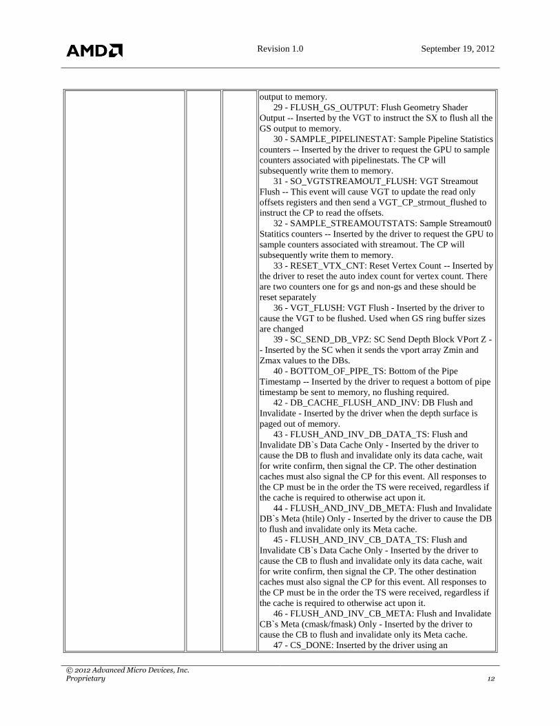
output to memory.
29 - FLUSH_GS_OUTPUT: Flush Geometry Shader
Output -- Inserted by the VGT to instruct the SX to flush all the
GS output to memory.
30 - SAMPLE_PIPELINESTAT: Sample Pipeline Statistics
counters -- Inserted by the driver to request the GPU to sample
counters associated with pipelinestats. The CP will
subsequently write them to memory.
31 - SO_VGTSTREAMOUT_FLUSH: VGT Streamout
Flush -- This event will cause VGT to update the read only
offsets registers and then send a VGT_CP_strmout_flushed to
instruct the CP to read the offsets.
32 - SAMPLE_STREAMOUTSTATS: Sample Streamout0
Statitics counters -- Inserted by the driver to request the GPU to
sample counters associated with streamout. The CP will
subsequently write them to memory.
33 - RESET_VTX_CNT: Reset Vertex Count -- Inserted by
the driver to reset the auto index count for vertex count. There
are two counters one for gs and non-gs and these should be
reset separately
36 - VGT_FLUSH: VGT Flush - Inserted by the driver to
cause the VGT to be flushed. Used when GS ring buffer sizes
are changed
39 - SC_SEND_DB_VPZ: SC Send Depth Block VPort Z -
- Inserted by the SC when it sends the vport array Zmin and
Zmax values to the DBs.
40 - BOTTOM_OF_PIPE_TS: Bottom of the Pipe
Timestamp -- Inserted by the driver to request a bottom of pipe
timestamp be sent to memory, no flushing required.
42 - DB_CACHE_FLUSH_AND_INV: DB Flush and
Invalidate - Inserted by the driver when the depth surface is
paged out of memory.
43 - FLUSH_AND_INV_DB_DATA_TS: Flush and
Invalidate DB`s Data Cache Only - Inserted by the driver to
cause the DB to flush and invalidate only its data cache, wait
for write confirm, then signal the CP. The other destination
caches must also signal the CP for this event. All responses to
the CP must be in the order the TS were received, regardless if
the cache is required to otherwise act upon it.
44 - FLUSH_AND_INV_DB_META: Flush and Invalidate
DB`s Meta (htile) Only - Inserted by the driver to cause the DB
to flush and invalidate only its Meta cache.
45 - FLUSH_AND_INV_CB_DATA_TS: Flush and
Invalidate CB`s Data Cache Only - Inserted by the driver to
cause the CB to flush and invalidate only its data cache, wait
for write confirm, then signal the CP. The other destination
caches must also signal the CP for this event. All responses to
the CP must be in the order the TS were received, regardless if
the cache is required to otherwise act upon it.
46 - FLUSH_AND_INV_CB_META: Flush and Invalidate
CB`s Meta (cmask/fmask) Only - Inserted by the driver to
cause the CB to flush and invalidate only its Meta cache.
47 - CS_DONE: Inserted by the driver using an

Revision 1.0 September 19, 2012
© 2012 Advanced Micro Devices, Inc. Proprietary 13
EVENT_WRITE_EOS packet. The SQ, in response, will
generate a signal to indicate that all CS work prior to this point
has completed.
48 - PS_DONE: Inserted by the driver using an
EVENT_WRITE_EOS packet. The SQ, in response, will
generate a signal to indicate that all PS work prior to this point
has completed.
49 - FLUSH_AND_INV_CB_PIXEL_DATA: Flush and
invalidate CB`s pixel (render target) data in color cache. Does
not guarantee UAV(RAT) flush-and-inv, and does not flush the
cmask/fmask cache either. Typically would be inserted by the
driver before resolving or expanding an MSAA buffer. No
wait-idle is necessary between this flush and the subsequent
resolve/expand draw command.
51 - THREAD_TRACE_START: Enable thread trace in
SQ. Inserted by the driver.
52 - THREAD_TRACE_STOP: Enable thread trace in SQ.
Inserted by the driver.
54 - THREAD_TRACE_FLUSH: Flush the thread trace
buffer to memory. The flush is not guaranteed to have
completed until either (1) the GUI is idle, or (2) BOTH a
subsequent timestamp have been returned and
SQ_THREAD_TRACE_WPTR.BUSY reads 0.
55 - THREAD_TRACE_FINISH: Flush the thread trace
buffer to memory and reset the memory write address to the
value last written to SQ_THREAD_TRACE_BASE (which
may change the destination buffer). The flush is not guaranteed
to have completed until either (1) the GUI is idle, or (2) BOTH
a subsequent timestamp has been returned and
SQ_THREAD_TRACE_WPTR.BUSY reads 0. Only one of
these events may be present in the pipeline at a given time.
56 - PIXEL_PIPE_STAT_CONTROL: Controls which
pixel pipe counters to either dump or reset based on subsequent
events.
57 - PIXEL_PIPE_STAT_DUMP: Dumps the currently
selected pixel pipe counter to memory address specified in
event.
58 - PIXEL_PIPE_STAT_RESET: Resets the currently
select pixel pipe counter to default value.
ADDRESS_HI 26:18 none address bits 39:31 for zpass event
EXTENDED_EVENT 27 none 0 for single DW event, 1 for two DW event
VGT:VGT_GROUP_DECR · [R/W] · 32 bits · Access: 32 · GpuF0MMReg:0x28a2c
DESCRIPTION: THIS REGISTER IS IGNORED IN MAJOR MODE 0 FOR PRIM TYPES 0 THRU 21 !! This
register contains the amount by which the draw initiator index count is decremented for all groups taken from the
input stream except for the first group.
Field Name Bits Default Description
DECR 3:0 none Decrement amount for groups except the first
Revision 1.0 September 19, 2012
© 2012 Advanced Micro Devices, Inc. Proprietary 14
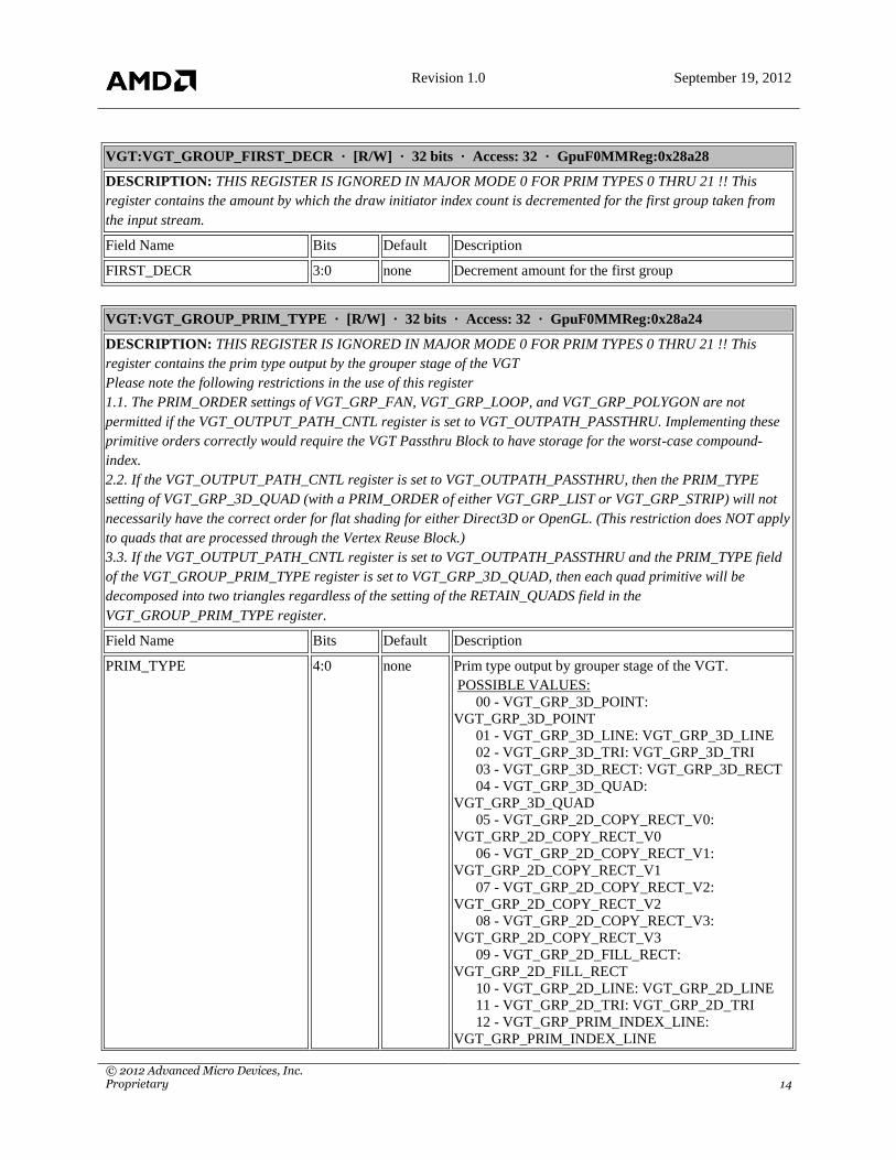
VGT:VGT_GROUP_FIRST_DECR · [R/W] · 32 bits · Access: 32 · GpuF0MMReg:0x28a28
DESCRIPTION: THIS REGISTER IS IGNORED IN MAJOR MODE 0 FOR PRIM TYPES 0 THRU 21 !! This
register contains the amount by which the draw initiator index count is decremented for the first group taken from
the input stream.
Field Name Bits Default Description
FIRST_DECR 3:0 none Decrement amount for the first group
VGT:VGT_GROUP_PRIM_TYPE · [R/W] · 32 bits · Access: 32 · GpuF0MMReg:0x28a24
DESCRIPTION: THIS REGISTER IS IGNORED IN MAJOR MODE 0 FOR PRIM TYPES 0 THRU 21 !! This
register contains the prim type output by the grouper stage of the VGT
Please note the following restrictions in the use of this register
1.1. The PRIM_ORDER settings of VGT_GRP_FAN, VGT_GRP_LOOP, and VGT_GRP_POLYGON are not
permitted if the VGT_OUTPUT_PATH_CNTL register is set to VGT_OUTPATH_PASSTHRU. Implementing these
primitive orders correctly would require the VGT Passthru Block to have storage for the worst-case compound-
index.
2.2. If the VGT_OUTPUT_PATH_CNTL register is set to VGT_OUTPATH_PASSTHRU, then the PRIM_TYPE
setting of VGT_GRP_3D_QUAD (with a PRIM_ORDER of either VGT_GRP_LIST or VGT_GRP_STRIP) will not
necessarily have the correct order for flat shading for either Direct3D or OpenGL. (This restriction does NOT apply
to quads that are processed through the Vertex Reuse Block.)
3.3. If the VGT_OUTPUT_PATH_CNTL register is set to VGT_OUTPATH_PASSTHRU and the PRIM_TYPE field
of the VGT_GROUP_PRIM_TYPE register is set to VGT_GRP_3D_QUAD, then each quad primitive will be
decomposed into two triangles regardless of the setting of the RETAIN_QUADS field in the
VGT_GROUP_PRIM_TYPE register.
Field Name Bits Default Description
PRIM_TYPE 4:0 none Prim type output by grouper stage of the VGT.
POSSIBLE VALUES:
00 - VGT_GRP_3D_POINT:
VGT_GRP_3D_POINT
01 - VGT_GRP_3D_LINE: VGT_GRP_3D_LINE
02 - VGT_GRP_3D_TRI: VGT_GRP_3D_TRI
03 - VGT_GRP_3D_RECT: VGT_GRP_3D_RECT
04 - VGT_GRP_3D_QUAD:
VGT_GRP_3D_QUAD
05 - VGT_GRP_2D_COPY_RECT_V0:
VGT_GRP_2D_COPY_RECT_V0
06 - VGT_GRP_2D_COPY_RECT_V1:
VGT_GRP_2D_COPY_RECT_V1
07 - VGT_GRP_2D_COPY_RECT_V2:
VGT_GRP_2D_COPY_RECT_V2
08 - VGT_GRP_2D_COPY_RECT_V3:
VGT_GRP_2D_COPY_RECT_V3
09 - VGT_GRP_2D_FILL_RECT:
VGT_GRP_2D_FILL_RECT
10 - VGT_GRP_2D_LINE: VGT_GRP_2D_LINE
11 - VGT_GRP_2D_TRI: VGT_GRP_2D_TRI
12 - VGT_GRP_PRIM_INDEX_LINE:
VGT_GRP_PRIM_INDEX_LINE

Revision 1.0 September 19, 2012
© 2012 Advanced Micro Devices, Inc. Proprietary 15
13 - VGT_GRP_PRIM_INDEX_TRI:
VGT_GRP_PRIM_INDEX_TRI
14 - VGT_GRP_PRIM_INDEX_QUAD:
VGT_GRP_PRIM_INDEX_QUAD
15 - VGT_GRP_3D_LINE_ADJ:
VGT_GRP_3D_LINE_ADJ
16 - VGT_GRP_3D_TRI_ADJ:
VGT_GRP_3D_TRI_ADJ
17 - VGT_GRP_3D_PATCH:
VGT_GRP_3D_PATCH
RETAIN_ORDER 14 none Resetting this bit to zero causes the Grouper within the
VGT to convert strips, fans, loops, and polygons into
regular lists in the vgt_grouper block. It also causes the
primitive indices to be re-ordered to have the provoking
vertex in the correct position. This bit should be set to
zero if the VGT_OUTPUT_PATH_CNTL register
specifies VGT_OUTPATH_VTX_REUSE or
VGT_OUTPATH_TESS_EN and the
VGT_DRAW_INITIATOR prim type is between 0 and
15, inclusive, (tri list, tri strip, tri fan, etc...). This bit is
implied to be zero for VGT_DRAW_INITIATOR prim
types 0 thru 15 if the Major Mode of the
VGT_DRAW_INIITIATOR is 0. If this bit is set for
prim types 0 thru 15, then the primitive index order from
the grouper will be retained and the indices will be
incorrect for loops, fans, and polygons. Note that if the
VGT_DRAW_INITIATOR.MAJOR_MODE is set to
MAJOR_MODE_1 and VGT_OUTPUT_PATH_CNTL
is set to VGT_OUTPATH_PASSTHRU and the
VGT_GROUP_PRIM_TYPE.PRIM_TYPE is set to
VGT_GRP_3D_TRI or VGT_GRP_2D_TRI and
VGT_GROUP_PRIM_TYPE.PRIM_ORDER is set to
VGT_GRP_STRIP, then the passthru block will perform
DX/OpenGL index re-ordering for tri-strips.
POSSIBLE VALUES:
00 - Reorder strip/fan/loop/polygon into lists with
correct provoking vertex
01 - Retain primitive index order as they appear in
the input stream
RETAIN_QUADS 15 none This bit can only be legally set if the
VGT_OUTPUT_PATH_CNTL register specifies the
Tessellation Engine and the Major Mode of the
VGT_DRAW_INITATOR is 1. The RETAIN_QUADS
bit indicates that quads should be passed intact to the
tessellation engine. If this bit is not set, then the quads
will be decomposed into triangles.
POSSIBLE VALUES:
00 - Decompose quads into triangles

Revision 1.0 September 19, 2012
© 2012 Advanced Micro Devices, Inc. Proprietary 16
01 - Retain quads (legal only for tessellation engine)
PRIM_ORDER 18:16 none Prim order output by grouper stage of the VGT.
POSSIBLE VALUES:
00 - VGT_GRP_LIST
01 - VGT_GRP_STRIP
02 - VGT_GRP_FAN
03 - VGT_GRP_LOOP
04 - VGT_GRP_POLYGON
VGT:VGT_GROUP_VECT_0_CNTL · [R/W] · 32 bits · Access: 32 · GpuF0MMReg:0x28a30
DESCRIPTION: THIS REGISTER IS IGNORED IN MAJOR MODE 0 FOR PRIM TYPES 0 THRU 21 !! This
register indicates, with bits flags, which components are relevant for vector 0 of a group. At least one component of
vector 0 must be indicated. This register also contains the stride of vector 0 (in 16-bit words) in the input stream and
the amount to shift the input stream (in 16-bit words) after extracting the vector.
Field Name Bits Default Description
COMP_X_EN 0 none Indicates that component X will be output from the
grouper for vector 0
POSSIBLE VALUES:
00 - disable
01 - enable
COMP_Y_EN 1 none Indicates that component Y will be output from the
grouper for vector 0
POSSIBLE VALUES:
00 - disable
01 - enable
COMP_Z_EN 2 none Indicates that component Z will be output from the
grouper for vector 0
POSSIBLE VALUES:
00 - disable
01 - enable
COMP_W_EN 3 none Indicates that component W will be output from the
grouper for vector 0
POSSIBLE VALUES:
00 - disable
01 - enable
STRIDE 15:8 none The stride of vector 0 data in the input stream (in 16-bit
words). Zero is NOT a legal value for an active vector.
See the programming guidelines for the situation in
which a vector uses no data from the shifter.
SHIFT 23:16 none The amount to shift the input stream after extracting
vector 0 (in 16-bit words). This field must be less than or
equal to the STRIDE field for proper shifter operation.
VGT:VGT_GROUP_VECT_0_FMT_CNTL · [R/W] · 32 bits · Access: 32 · GpuF0MMReg:0x28a38
DESCRIPTION: THIS REGISTER IS IGNORED IN MAJOR MODE 0 FOR PRIM TYPES 0 THRU 21 !!

Revision 1.0 September 19, 2012
© 2012 Advanced Micro Devices, Inc. Proprietary 17
This register controls how each enabled component of vector 0 of each group is extracted from the stream. If a
component is not enabled in the VGT_GROUP_VECT_0_CNTL register, then the settings for that component are
ignored. If a component conversion is set to VGT_GRP_INDEX_16 or VGT_GRP_INDEX_32, then that component
is treated as an index. It will be clamped to be within the min and max index values (see the VGT_MAX_VTX_INDX
and the VGT_MIN_VTX_INDX registers). It will also be offset with the index offset value (see the
VGT_INDX_OFFSET register). If the conversion is set to VGT_GRP_INDEX_32, then the upper byte of the 32-bit
value will be masked to zeros prior to clamping, offsetting, and fix-to-float conversion. The component conversion
for each component is passed to the Output Block of the VGT where is it used to determine the appropriate fix-to-
float conversion for the particular component
The offset field in the VGT_GROUP_VECT_0_FMT_CTNL register specifies where the component should be
extracted from the shift register. This specification allows components to be re-ordered with vector 0; however, they
cannot be re-order between vector 0 and vector 1, nor can they be re-ordered between groups
Field Name Bits Default Description
X_CONV 3:0 none X Component Determination.
POSSIBLE VALUES:
00 - VGT_GRP_INDEX_16:
VGT_GRP_INDEX_16 16 bits from stream with index
offset and clamp
01 - VGT_GRP_INDEX_32:
VGT_GRP_INDEX_32 32 bits from stream with index
offset and clamp
02 - VGT_GRP_UINT_16: VGT_GRP_UINT_16 16
bits from stream as unsigned int
03 - VGT_GRP_UINT_32: VGT_GRP_UINT_32 32
bits from stream as unsigned int
04 - VGT_GRP_SINT_16: VGT_GRP_SINT_16 16
bits from stream as signed int
05 - VGT_GRP_SINT_32: VGT_GRP_SINT_32 32
bits from stream as signed int
06 - VGT_GRP_FLOAT_32:
VGT_GRP_FLOAT_32 32 bits from stream as float
07 - VGT_GRP_AUTO_PRIM:
VGT_GRP_AUTO_PRIM 24 bits from auto primitive
counter
08 - VGT_GRP_FIX_1_23_TO_FLOAT:
VGT_GRP_FIX_1_23_TO_FLOAT 24 bit barycentric
value from tessellation engine
X_OFFSET 7:4 none X Component Offset. This field is the offset, in 16-bit
words, of the X component in the input cycle.
Y_CONV 11:8 none Y Component Determination. See the X component
determination field for description.
POSSIBLE VALUES:
00 - VGT_GRP_INDEX_16:
VGT_GRP_INDEX_16 16 bits from stream with index
offset and clamp
01 - VGT_GRP_INDEX_32:
VGT_GRP_INDEX_32 32 bits from stream with index
offset and clamp
02 - VGT_GRP_UINT_16: VGT_GRP_UINT_16 16

Revision 1.0 September 19, 2012
© 2012 Advanced Micro Devices, Inc. Proprietary 18
bits from stream as unsigned int
03 - VGT_GRP_UINT_32: VGT_GRP_UINT_32 32
bits from stream as unsigned int
04 - VGT_GRP_SINT_16: VGT_GRP_SINT_16 16
bits from stream as signed int
05 - VGT_GRP_SINT_32: VGT_GRP_SINT_32 32
bits from stream as signed int
06 - VGT_GRP_FLOAT_32:
VGT_GRP_FLOAT_32 32 bits from stream as float
07 - VGT_GRP_AUTO_PRIM:
VGT_GRP_AUTO_PRIM 24 bits from auto primitive
counter
08 - VGT_GRP_FIX_1_23_TO_FLOAT:
VGT_GRP_FIX_1_23_TO_FLOAT 24 bit barycentric
value from tessellation engine
Y_OFFSET 15:12 none Y Component Offset. This field is the offset, in 16-bit
words, of the Y component in the input cycle.
Z_CONV 19:16 none Z Component Determination. See the X component
determination field for description.
POSSIBLE VALUES:
00 - VGT_GRP_INDEX_16:
VGT_GRP_INDEX_16 16 bits from stream with index
offset and clamp
01 - VGT_GRP_INDEX_32:
VGT_GRP_INDEX_32 32 bits from stream with index
offset and clamp
02 - VGT_GRP_UINT_16: VGT_GRP_UINT_16 16
bits from stream as unsigned int
03 - VGT_GRP_UINT_32: VGT_GRP_UINT_32 32
bits from stream as unsigned int
04 - VGT_GRP_SINT_16: VGT_GRP_SINT_16 16
bits from stream as signed int
05 - VGT_GRP_SINT_32: VGT_GRP_SINT_32 32
bits from stream as signed int
06 - VGT_GRP_FLOAT_32:
VGT_GRP_FLOAT_32 32 bits from stream as float
07 - VGT_GRP_AUTO_PRIM:
VGT_GRP_AUTO_PRIM 24 bits from auto primitive
counter
08 - VGT_GRP_FIX_1_23_TO_FLOAT:
VGT_GRP_FIX_1_23_TO_FLOAT 24 bit barycentric
value from tessellation engine
Z_OFFSET 23:20 none Z Component Offset. This field is the offset, in 16-bit
words, of the Z component in the input cycle.
W_CONV 27:24 none W Component Determination. See the X component
determination field for description.
POSSIBLE VALUES:
00 - VGT_GRP_INDEX_16:
VGT_GRP_INDEX_16 16 bits from stream with index
offset and clamp
01 - VGT_GRP_INDEX_32:
Revision 1.0 September 19, 2012
© 2012 Advanced Micro Devices, Inc. Proprietary 19
VGT_GRP_INDEX_32 32 bits from stream with index
offset and clamp
02 - VGT_GRP_UINT_16: VGT_GRP_UINT_16 16
bits from stream as unsigned int
03 - VGT_GRP_UINT_32: VGT_GRP_UINT_32 32
bits from stream as unsigned int
04 - VGT_GRP_SINT_16: VGT_GRP_SINT_16 16
bits from stream as signed int
05 - VGT_GRP_SINT_32: VGT_GRP_SINT_32 32
bits from stream as signed int
06 - VGT_GRP_FLOAT_32:
VGT_GRP_FLOAT_32 32 bits from stream as float
07 - VGT_GRP_AUTO_PRIM:
VGT_GRP_AUTO_PRIM 24 bits from auto primitive
counter
08 - VGT_GRP_FIX_1_23_TO_FLOAT:
VGT_GRP_FIX_1_23_TO_FLOAT 24 bit barycentric
value from tessellation engine
W_OFFSET 31:28 none W Component Offset. This field is the offset, in 16-bit
words, of the Z component in the input cycle.
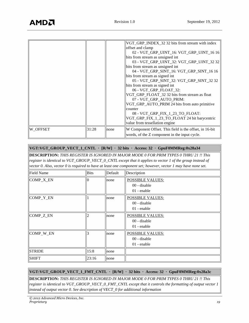
VGT:VGT_GROUP_VECT_1_CNTL · [R/W] · 32 bits · Access: 32 · GpuF0MMReg:0x28a34
DESCRIPTION: THIS REGISTER IS IGNORED IN MAJOR MODE 0 FOR PRIM TYPES 0 THRU 21 !! This
register is identical to VGT_GROUP_VECT_0_CNTL except that it applies to vector 1 of the group instead of
vector 0. Also, vector 0 is required to have at least one component set; however, vector 1 may have none set.
Field Name Bits Default Description
COMP_X_EN 0 none POSSIBLE VALUES:
00 - disable
01 - enable
COMP_Y_EN 1 none POSSIBLE VALUES:
00 - disable
01 - enable
COMP_Z_EN 2 none POSSIBLE VALUES:
00 - disable
01 - enable
COMP_W_EN 3 none POSSIBLE VALUES:
00 - disable
01 - enable
STRIDE 15:8 none
SHIFT 23:16 none
VGT:VGT_GROUP_VECT_1_FMT_CNTL · [R/W] · 32 bits · Access: 32 · GpuF0MMReg:0x28a3c
DESCRIPTION: THIS REGISTER IS IGNORED IN MAJOR MODE 0 FOR PRIM TYPES 0 THRU 21 !! This
register is identical to VGT_GROUP_VECT_0_FMT_CNTL except that it controls the formatting of output vector 1
instead of output vector 0. See description of VECT_0 for additional information

Revision 1.0 September 19, 2012
© 2012 Advanced Micro Devices, Inc. Proprietary 20
Field Name Bits Default Description
X_CONV 3:0 none POSSIBLE VALUES:
00 - VGT_GRP_INDEX_16:
VGT_GRP_INDEX_16 16 bits from stream with index
offset and clamp
01 - VGT_GRP_INDEX_32:
VGT_GRP_INDEX_32 32 bits from stream with index
offset and clamp
02 - VGT_GRP_UINT_16: VGT_GRP_UINT_16 16
bits from stream as unsigned int
03 - VGT_GRP_UINT_32: VGT_GRP_UINT_32 32
bits from stream as unsigned int
04 - VGT_GRP_SINT_16: VGT_GRP_SINT_16 16
bits from stream as signed int
05 - VGT_GRP_SINT_32: VGT_GRP_SINT_32 32
bits from stream as signed int
06 - VGT_GRP_FLOAT_32:
VGT_GRP_FLOAT_32 32 bits from stream as float
07 - VGT_GRP_AUTO_PRIM:
VGT_GRP_AUTO_PRIM 24 bits from auto primitive
counter
08 - VGT_GRP_FIX_1_23_TO_FLOAT:
VGT_GRP_FIX_1_23_TO_FLOAT 24 bit barycentric
value from tessellation engine
X_OFFSET 7:4 none
Y_CONV 11:8 none POSSIBLE VALUES:
00 - VGT_GRP_INDEX_16:
VGT_GRP_INDEX_16 16 bits from stream with index
offset and clamp
01 - VGT_GRP_INDEX_32:
VGT_GRP_INDEX_32 32 bits from stream with index
offset and clamp
02 - VGT_GRP_UINT_16: VGT_GRP_UINT_16 16
bits from stream as unsigned int
03 - VGT_GRP_UINT_32: VGT_GRP_UINT_32 32
bits from stream as unsigned int
04 - VGT_GRP_SINT_16: VGT_GRP_SINT_16 16
bits from stream as signed int
05 - VGT_GRP_SINT_32: VGT_GRP_SINT_32 32
bits from stream as signed int
06 - VGT_GRP_FLOAT_32:
VGT_GRP_FLOAT_32 32 bits from stream as float
07 - VGT_GRP_AUTO_PRIM:
VGT_GRP_AUTO_PRIM 24 bits from auto primitive
counter

Revision 1.0 September 19, 2012
© 2012 Advanced Micro Devices, Inc. Proprietary 21
08 - VGT_GRP_FIX_1_23_TO_FLOAT:
VGT_GRP_FIX_1_23_TO_FLOAT 24 bit barycentric
value from tessellation engine
Y_OFFSET 15:12 none
Z_CONV 19:16 none POSSIBLE VALUES:
00 - VGT_GRP_INDEX_16:
VGT_GRP_INDEX_16 16 bits from stream with index
offset and clamp
01 - VGT_GRP_INDEX_32:
VGT_GRP_INDEX_32 32 bits from stream with index
offset and clamp
02 - VGT_GRP_UINT_16: VGT_GRP_UINT_16 16
bits from stream as unsigned int
03 - VGT_GRP_UINT_32: VGT_GRP_UINT_32 32
bits from stream as unsigned int
04 - VGT_GRP_SINT_16: VGT_GRP_SINT_16 16
bits from stream as signed int
05 - VGT_GRP_SINT_32: VGT_GRP_SINT_32 32
bits from stream as signed int
06 - VGT_GRP_FLOAT_32:
VGT_GRP_FLOAT_32 32 bits from stream as float
07 - VGT_GRP_AUTO_PRIM:
VGT_GRP_AUTO_PRIM 24 bits from auto primitive
counter
08 - VGT_GRP_FIX_1_23_TO_FLOAT:
VGT_GRP_FIX_1_23_TO_FLOAT 24 bit barycentric
value from tessellation engine
Z_OFFSET 23:20 none
W_CONV 27:24 none POSSIBLE VALUES:
00 - VGT_GRP_INDEX_16:
VGT_GRP_INDEX_16 16 bits from stream with index
offset and clamp
01 - VGT_GRP_INDEX_32:
VGT_GRP_INDEX_32 32 bits from stream with index
offset and clamp
02 - VGT_GRP_UINT_16: VGT_GRP_UINT_16 16
bits from stream as unsigned int
03 - VGT_GRP_UINT_32: VGT_GRP_UINT_32 32
bits from stream as unsigned int
04 - VGT_GRP_SINT_16: VGT_GRP_SINT_16 16
bits from stream as signed int
05 - VGT_GRP_SINT_32: VGT_GRP_SINT_32 32
bits from stream as signed int
06 - VGT_GRP_FLOAT_32:
VGT_GRP_FLOAT_32 32 bits from stream as float

Revision 1.0 September 19, 2012
© 2012 Advanced Micro Devices, Inc. Proprietary 22
07 - VGT_GRP_AUTO_PRIM:
VGT_GRP_AUTO_PRIM 24 bits from auto primitive
counter
08 - VGT_GRP_FIX_1_23_TO_FLOAT:
VGT_GRP_FIX_1_23_TO_FLOAT 24 bit barycentric
value from tessellation engine
W_OFFSET 31:28 none
VGT:VGT_GSVS_RING_ITEMSIZE · [R/W] · 32 bits · Access: 32 · GpuF0MMReg:0x28ab0
DESCRIPTION: Size of each primitive written to the GSVS Ring buffer
Field Name Bits Default Description
ITEMSIZE 14:0 none Size specified in dwords. Must be ast least 4 dwords and
must be a multiple of 4 dwords
VGT:VGT_GSVS_RING_OFFSET_1 · [R/W] · 32 bits · Access: 32 · GpuF0MMReg:0x28a60
Field Name Bits Default Description
OFFSET 14:0 none
VGT:VGT_GSVS_RING_OFFSET_2 · [R/W] · 32 bits · Access: 32 · GpuF0MMReg:0x28a64
Field Name Bits Default Description
OFFSET 14:0 none
VGT:VGT_GSVS_RING_OFFSET_3 · [R/W] · 32 bits · Access: 32 · GpuF0MMReg:0x28a68
Field Name Bits Default Description
OFFSET 14:0 none
VGT:VGT_GSVS_RING_SIZE · [R/W] · 32 bits · Access: 32 · GpuF0MMReg:0x30904
DESCRIPTION: Size of the GSVS Ring buffer in multiples of 256 bytes
Field Name Bits Default Description
MEM_SIZE 31:0 none For dual shader engine parts, the size must be set to a
multiple of 512 bytes since half of the ring is used for
each SE
VGT:VGT_GS_INSTANCE_CNT · [R/W] · 32 bits · Access: 32 · GpuF0MMReg:0x28b90
DESCRIPTION: Specifies the amount of GS prim instancing
Field Name Bits Default Description
ENABLE 0 none Enable GS instancing
POSSIBLE VALUES:
00 - gs_instance_disable

Revision 1.0 September 19, 2012
© 2012 Advanced Micro Devices, Inc. Proprietary 23
01 - gs_instance_enable
CNT 8:2 none Number of GS prim instances, if set to 0 gs instancing is
treated as off, no instance id provided
VGT:VGT_GS_MAX_VERT_OUT · [R/W] · 32 bits · Access: 32 · GpuF0MMReg:0x28b38
DESCRIPTION: VGT max verts output by the GS for each prim
Field Name Bits Default Description
MAX_VERT_OUT 10:0 none GS Scenario C
When in scenario C, the VGT uses this register to
determine how many GS output verts to create. The PA
is responsible for construction of the primitives based on
what the shader does.
GS Scenario G
When in scenario G and 10xx on, the VGT will clamp
the number of emits from the GS shader against this
value (earlier there was an automatic clamp against a
default of 1024). There is no default value for this
register on reset, the API should program this to 1024 at
initialization if the feature is not required.
VGT:VGT_GS_MODE · [R/W] · 32 bits · Access: 32 · GpuF0MMReg:0x28a40
DESCRIPTION: VGT Geometry Shader Control Register
Field Name Bits Default Description
MODE 2:0 none Indicates which of the GS scenarios are enabled
POSSIBLE VALUES:
00 - GS_OFF: GS_OFF
01 - GS_SCENARIO_A: GS_SCENARIO_A
02 - GS_SCENARIO_B: GS_SCENARIO_B
03 - GS_SCENARIO_G: GS_SCENARIO_G
04 - GS_SCENARIO_C: GS_SCENARIO_C
05 - SPRITE_EN: SPRITE_EN
CUT_MODE 5:4 none 00: more than 512 gs emit vertices, 01: more than 256 and
less than equal to 512 emit vertices, 10:more than 128 and
less than or equal to 256 gs emit vertices, 11: less than or
equal to 128 gs emit vertices
POSSIBLE VALUES:
00 - GS_CUT_1024
01 - GS_CUT_512
02 - GS_CUT_256
03 - GS_CUT_128
GS_C_PACK_EN 11 none Indicates whether to pack the indices when in scenario c
mode
ES_PASSTHRU 13 none sets to one if VS shader is passthru when GS scenario G is

Revision 1.0 September 19, 2012
© 2012 Advanced Micro Devices, Inc. Proprietary 24
used
POSSIBLE VALUES:
00 - passthru_dis
01 - passthru_en
COMPUTE_MODE 14 none set to one if GS shader is to be skipped when GS scenario
G is used. Used for GPGPU.
POSSIBLE VALUES:
00 - compute_dis
01 - compute_en
FAST_COMPUTE_MODE 15 none set to one to enable one ES thread per clock.
COMPUTE_MODE must also be 1.
POSSIBLE VALUES:
00 - fast_compute_dis
01 - fast_compute_en
ELEMENT_INFO_EN 16 none set to one to have parts of vertex id, instance id, and step
rate overwrite the MSBs of the ES thread`s base address
POSSIBLE VALUES:
00 - element_info_en_dis
01 - element_info_en_en
PARTIAL_THD_AT_EOI 17 none set to one to have partial threads submitted at the end of an
instance
POSSIBLE VALUES:
00 - partial_thd_at_eoi_dis
01 - partial_thd_at_eoi_en
SUPPRESS_CUTS 18 none set to one to suppress cuts. this can be used with points to
allow for the max GS wave count regardless of the max
vert count. CUT_MODE must be set to 3 to get the full
benefit.
POSSIBLE VALUES:
00 - suppress_cuts_dis
01 - suppress_cuts_en
ES_WRITE_OPTIMIZE 19 none Controls whether the ESGS ring is omtimized for write
combining. 0 is the old (9xx) mode
POSSIBLE VALUES:
00 - disable write combining address pattern
01 - enable write combining address pattern
GS_WRITE_OPTIMIZE 20 none Controls whether the GSVS ring is omtimized for write
combining. 0 is the old (9xx) mode
POSSIBLE VALUES:
00 - disable write combining address pattern
01 - enable write combining address pattern
ONCHIP 22:21 none Controls whether the ESGS and GSVS ring buffers are
maintained in LDS or in offchip memory
POSSIBLE VALUES:
00 - 0 - Offchip GS
03 - 3 - ES and GS are onchip

Revision 1.0 September 19, 2012
© 2012 Advanced Micro Devices, Inc. Proprietary 25
VGT:VGT_GS_ONCHIP_CNTL · [R/W] · 32 bits · Access: 32 · GpuF0MMReg:0x28a44
DESCRIPTION: VGT Geometry Shader Control Register for on chip mode
Field Name Bits Default Description
ES_VERTS_PER_SUBGRP 10:0 none The worst case number of ES vertices needed to create
the GS prims specified in GS_PRIMS_PER_SUBGRP
GS_PRIMS_PER_SUBGRP 21:11 none The number of GS prims that can fit in the LDS
VGT:VGT_GS_OUT_PRIM_TYPE · [R/W] · 32 bits · Access: 32 · GpuF0MMReg:0x28a6c
DESCRIPTION: VGT GS output primitive type
Field Name Bits Default Description
OUTPRIM_TYPE 5:0 0x0 GS output primitive type
OUTPRIM_TYPE_1 13:8 0x0 GS output primitive type for stream 1
OUTPRIM_TYPE_2 21:16 0x0 GS output primitive type for stream 2
OUTPRIM_TYPE_3 27:22 0x0 GS output primitive type for stream 3
UNIQUE_TYPE_PER_STREAM 31 0x0 If 1 OUTPRIM_TYPE field represents stream 0. If 0
OUTPRIM_TYPE field is for all streams.
VGT:VGT_GS_PER_ES · [R/W] · 32 bits · Access: 32 · GpuF0MMReg:0x28a54
DESCRIPTION: Maximum GS prims per ES thread
Field Name Bits Default Description
GS_PER_ES 10:0 none Maximum number of GS prims per ES thread
When PARTIAL_ES_WAVE_ON is set to 0,
(gs_per_es/primgroup_size) must be lesser than
(GPU_VGT__GS_TABLE_DEPTH - 3)
VGT:VGT_GS_PER_VS · [R/W] · 32 bits · Access: 32 · GpuF0MMReg:0x28a5c
DESCRIPTION: Maximum GS threads per VS thread
Field Name Bits Default Description
GS_PER_VS 3:0 none Maximum number of GS threads per VS thread
VGT:VGT_GS_VERTEX_REUSE · [R/W] · 32 bits · Access: 32 · GpuF0MMReg:0x88d4
DESCRIPTION: reusability for GS path, it has nothing to do with number of good simd
Field Name Bits Default Description
VERT_REUSE 4:0 0x10 Reusability number for GS input prims. Can be set to
either 0, or from 4-16 in normal GS G mode of
operation, but it must be at least 4 if the tessellation
output is piped to the GS path

Revision 1.0 September 19, 2012
© 2012 Advanced Micro Devices, Inc. Proprietary 26
VGT:VGT_GS_VERT_ITEMSIZE · [R/W] · 32 bits · Access: 32 · GpuF0MMReg:0x28b5c
DESCRIPTION: Size of each vertex for Stream 0 written to the GSVS Ring buffer
Field Name Bits Default Description
ITEMSIZE 14:0 none Size specified in dwords.
VGT:VGT_GS_VERT_ITEMSIZE_1 · [R/W] · 32 bits · Access: 32 · GpuF0MMReg:0x28b60
DESCRIPTION: Size of each vertex for Stream 1 written to the GSVS Ring buffer
Field Name Bits Default Description
ITEMSIZE 14:0 none Size specified in dwords.
VGT:VGT_GS_VERT_ITEMSIZE_2 · [R/W] · 32 bits · Access: 32 · GpuF0MMReg:0x28b64
DESCRIPTION: Size of each vertex for Stream 2 written to the GSVS Ring buffer
Field Name Bits Default Description
ITEMSIZE 14:0 none Size specified in dwords.
VGT:VGT_GS_VERT_ITEMSIZE_3 · [R/W] · 32 bits · Access: 32 · GpuF0MMReg:0x28b68
DESCRIPTION: Size of each vertex for Stream 3 written to the GSVS Ring buffer
Field Name Bits Default Description
ITEMSIZE 14:0 none Size specified in dwords.
VGT:VGT_HOS_CNTL · [R/W] · 32 bits · Access: 32 · GpuF0MMReg:0x28a14
DESCRIPTION: This register controls the behavior of the Tessellation Engine block at the backend of the VGT.
This register is relevant only if the VGT_OUTPUT_PATH_CNTL register specifies the Tessellation Engine block for
the VGT backend path. Note that the tessellation engine is enabled by selecting the tessellation engine path in the
VGT_OUTPUT_PATH_CNTL register as opposed to the single enable bit that was used in previous architectures.
Field Name Bits Default Description
TESS_MODE 1:0 none Tessellation Mode
0 : Discrete
1 : Continuous
2 : Adaptive
VGT:VGT_HOS_MAX_TESS_LEVEL · [R/W] · 32 bits · Access: 32 · GpuF0MMReg:0x28a18
DESCRIPTION: This register specifies a Max tessellation level clamp that the hardware will apply to fetched Tess
Factors.
Field Name Bits Default Description
MAX_TESS 31:0 none Values in the range (0.0, 64.0) are legal. If the incoming
factor is a Nan, a negative number or Zero, it is not
clamped against this value.

Revision 1.0 September 19, 2012
© 2012 Advanced Micro Devices, Inc. Proprietary 27
VGT:VGT_HOS_MIN_TESS_LEVEL · [R/W] · 32 bits · Access: 32 · GpuF0MMReg:0x28a1c
DESCRIPTION: This register specifies a Min tessellation level clamp that the hardware will apply to fetched Tess
Factors.
Field Name Bits Default Description
MIN_TESS 31:0 none Values in the range (0.0, 64.0) are legal. If the incoming
factor is a Nan, a negative number or Zero, it is not
clamped against this value.
VGT:VGT_HOS_REUSE_DEPTH · [R/W] · 32 bits · Access: 32 · GpuF0MMReg:0x28a20
DESCRIPTION: This register tells the tessellation how many of most recently submitted vertices it can reuse.
This register is relevant only when the VGT_OUT_CNTL register specifies `Tessellation Engine` in the Path Select
field.
Field Name Bits Default Description
REUSE_DEPTH 7:0 none Set this register to 2 more than the desired reuse depth.
Ideally this should be set to 16 and not changed
VGT:VGT_HS_OFFCHIP_PARAM · [R/W] · 32 bits · Access: 32 · GpuF0MMReg:0x3093c
DESCRIPTION: Control parameters for the Offchip HS mode of operation
Field Name Bits Default Description
OFFCHIP_BUFFERING 8:0 0x0 Amount of offchip buffering available, ranges from 1 to
64 8K dword buffers.
OFFCHIP_GRANULARITY 10:9 0x0 POSSIBLE VALUES:
00 - 8K dwords
01 - 4K dwords
02 - 2K dwords
03 - 1K dwords
VGT:VGT_INDEX_TYPE · [W] · 32 bits · Access: 32 · GpuF0MMReg:0x3090c
DESCRIPTION: VGT Index Type
Field Name Bits Default Description
INDEX_TYPE 1:0 none Index Type (applicable to prim types 0-28 only).
If the Source Select field is set to `Auto-increment Index`
mode, then this field is ignored and the index type is 32-
bits per index
POSSIBLE VALUES:
00 - DI_INDEX_SIZE_16_BIT:
DI_INDEX_SIZE_16_BIT 16 bits per index
01 - DI_INDEX_SIZE_32_BIT:
DI_INDEX_SIZE_32_BIT 32 bits per index
Revision 1.0 September 19, 2012
© 2012 Advanced Micro Devices, Inc. Proprietary 28
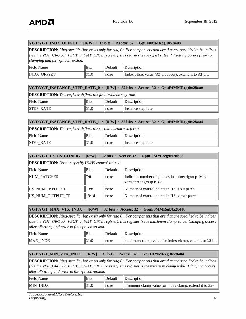
VGT:VGT_INDX_OFFSET · [R/W] · 32 bits · Access: 32 · GpuF0MMReg:0x28408
DESCRIPTION: Ring-specific (but exists only for ring 0). For components that are that are specified to be indices
(see the VGT_GROUP_VECT_0_FMT_CNTL register), this register is the offset value. Offsetting occurs prior to
clamping and fix->flt conversion.
Field Name Bits Default Description
INDX_OFFSET 31:0 none Index offset value (32-bit adder), extend it to 32-bits
VGT:VGT_INSTANCE_STEP_RATE_0 · [R/W] · 32 bits · Access: 32 · GpuF0MMReg:0x28aa0
DESCRIPTION: This register defines the first instance step rate
Field Name Bits Default Description
STEP_RATE 31:0 none Instance step rate
VGT:VGT_INSTANCE_STEP_RATE_1 · [R/W] · 32 bits · Access: 32 · GpuF0MMReg:0x28aa4
DESCRIPTION: This register defines the second instance step rate
Field Name Bits Default Description
STEP_RATE 31:0 none Instance step rate
VGT:VGT_LS_HS_CONFIG · [R/W] · 32 bits · Access: 32 · GpuF0MMReg:0x28b58
DESCRIPTION: Used to specify LS/HS control values
Field Name Bits Default Description
NUM_PATCHES 7:0 none Indicates number of patches in a threadgroup. Max
verts/threadgroup is 4k.
HS_NUM_INPUT_CP 13:8 none Number of control points in HS input patch
HS_NUM_OUTPUT_CP 19:14 none Number of control points in HS output patch
VGT:VGT_MAX_VTX_INDX · [R/W] · 32 bits · Access: 32 · GpuF0MMReg:0x28400
DESCRIPTION: Ring-specific (but exists only for ring 0). For components that are that are specified to be indices
(see the VGT_GROUP_VECT_0_FMT_CNTL register), this register is the maximum clamp value. Clamping occurs
after offsetting and prior to fix->flt conversion.
Field Name Bits Default Description
MAX_INDX 31:0 none maximum clamp value for index clamp, exten it to 32-bit
VGT:VGT_MIN_VTX_INDX · [R/W] · 32 bits · Access: 32 · GpuF0MMReg:0x28404
DESCRIPTION: Ring-specific (but exists only for ring 0). For components that are that are specified to be indices
(see the VGT_GROUP_VECT_0_FMT_CNTL register), this register is the minimum clamp value. Clamping occurs
after offsetting and prior to fix->flt conversion.
Field Name Bits Default Description
MIN_INDX 31:0 none minimum clamp value for index clamp, extend it to 32-
Revision 1.0 September 19, 2012
© 2012 Advanced Micro Devices, Inc. Proprietary 29
bits
VGT:VGT_MULTI_PRIM_IB_RESET_EN · [R/W] · 32 bits · Access: 32 · GpuF0MMReg:0x28a94
DESCRIPTION: This register enabling reseting of prim based on reset index
Field Name Bits Default Description
RESET_EN 0 none IF SET, THEN RESET INDEX IS USED FOR
RESETING A PRIM
POSSIBLE VALUES:
00 - multi_prim reset off
01 - multi_prim reset on
VGT:VGT_MULTI_PRIM_IB_RESET_INDX · [R/W] · 32 bits · Access: 32 · GpuF0MMReg:0x2840c
DESCRIPTION: This register specifies the 32-bit index value used to reset the primitive order (strip/fan/polygon)
Field Name Bits Default Description
RESET_INDX 31:0 none If this value matches an index in the IB, a new primitive
set is started.
VGT:VGT_NUM_INDICES · [W] · 32 bits · Access: 32 · GpuF0MMReg:0x30930
DESCRIPTION: VGT Number of Indices
Field Name Bits Default Description
NUM_INDICES 31:0 none This field indicates the number of indices to process for
this draw initiator. Note this count is not necessarily the
count of the primitives. It is also not the index buffer size
in memory.When using Dx11 compute shaders, this
register needs to be written by the driver to the product
of x,y,z which are the 3 dimensions that define a
compute shader threadgroup size.
VGT:VGT_NUM_INSTANCES · [W] · 32 bits · Access: 32 · GpuF0MMReg:0x30934
DESCRIPTION: VGT Number of Instances
Field Name Bits Default Description
NUM_INSTANCES 31:0 none Number of instances in a draw call, if set to zero, it is
interpreted as 1. The maximum value is 2^32-1
VGT:VGT_OUTPUT_PATH_CNTL · [R/W] · 32 bits · Access: 32 · GpuF0MMReg:0x28a10
DESCRIPTION: THIS REGISTER IS IGNORED IN MAJOR MODE 0 FOR PRIM TYPES 0 THRU 21 !! This
register selects which backend path will be used by the VGT block.
Field Name Bits Default Description
PATH_SELECT 2:0 none This field indicates the VGT back-end path to be used.
POSSIBLE VALUES:
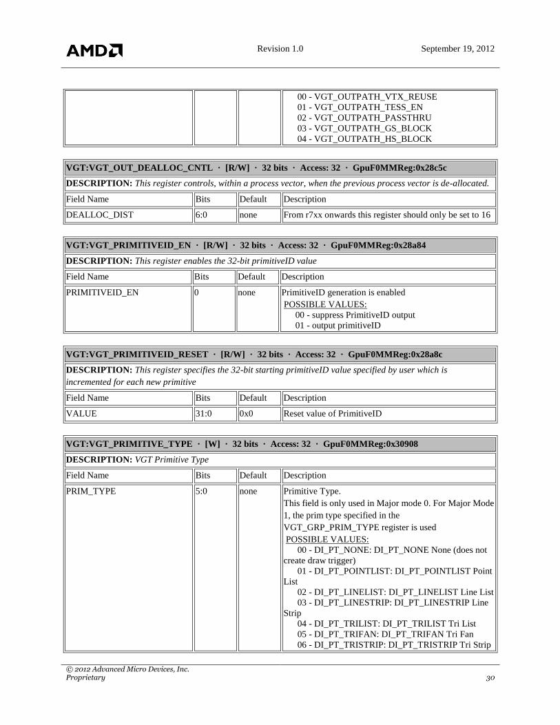
Revision 1.0 September 19, 2012
© 2012 Advanced Micro Devices, Inc. Proprietary 30
00 - VGT_OUTPATH_VTX_REUSE
01 - VGT_OUTPATH_TESS_EN
02 - VGT_OUTPATH_PASSTHRU
03 - VGT_OUTPATH_GS_BLOCK
04 - VGT_OUTPATH_HS_BLOCK
VGT:VGT_OUT_DEALLOC_CNTL · [R/W] · 32 bits · Access: 32 · GpuF0MMReg:0x28c5c
DESCRIPTION: This register controls, within a process vector, when the previous process vector is de-allocated.
Field Name Bits Default Description
DEALLOC_DIST 6:0 none From r7xx onwards this register should only be set to 16
VGT:VGT_PRIMITIVEID_EN · [R/W] · 32 bits · Access: 32 · GpuF0MMReg:0x28a84
DESCRIPTION: This register enables the 32-bit primitiveID value
Field Name Bits Default Description
PRIMITIVEID_EN 0 none PrimitiveID generation is enabled
POSSIBLE VALUES:
00 - suppress PrimitiveID output
01 - output primitiveID
VGT:VGT_PRIMITIVEID_RESET · [R/W] · 32 bits · Access: 32 · GpuF0MMReg:0x28a8c
DESCRIPTION: This register specifies the 32-bit starting primitiveID value specified by user which is
incremented for each new primitive
Field Name Bits Default Description
VALUE 31:0 0x0 Reset value of PrimitiveID
VGT:VGT_PRIMITIVE_TYPE · [W] · 32 bits · Access: 32 · GpuF0MMReg:0x30908
DESCRIPTION: VGT Primitive Type
Field Name Bits Default Description
PRIM_TYPE 5:0 none Primitive Type.
This field is only used in Major mode 0. For Major Mode
1, the prim type specified in the
VGT_GRP_PRIM_TYPE register is used
POSSIBLE VALUES:
00 - DI_PT_NONE: DI_PT_NONE None (does not
create draw trigger)
01 - DI_PT_POINTLIST: DI_PT_POINTLIST Point
List
02 - DI_PT_LINELIST: DI_PT_LINELIST Line List
03 - DI_PT_LINESTRIP: DI_PT_LINESTRIP Line
Strip
04 - DI_PT_TRILIST: DI_PT_TRILIST Tri List
05 - DI_PT_TRIFAN: DI_PT_TRIFAN Tri Fan
06 - DI_PT_TRISTRIP: DI_PT_TRISTRIP Tri Strip

Revision 1.0 September 19, 2012
© 2012 Advanced Micro Devices, Inc. Proprietary 31
09 - DI_PT_PATCH: DI_PT_PATCH Patch prim
type used in conjunction with HS_NUM_INPUT_CP
10 - DI_PT_LINELIST_ADJ:
DI_PT_LINELIST_ADJ Adjacent Line List
11 - DI_PT_LINESTRIP_ADJ:
DI_PT_LINESTRIP_ADJ Adjacent Line Strip
12 - DI_PT_TRILIST_ADJ: DI_PT_TRILIST_ADJ
Adjacent Tri List
13 - DI_PT_TRISTRIP_ADJ:
DI_PT_TRISTRIP_ADJ Adjacent Tri Strip
16 - DI_PT_TRI_WITH_WFLAGS:
DI_PT_TRI_WITH_WFLAGS Tri List w/Flags (legacy
R128)
17 - DI_PT_RECTLIST: DI_PT_RECTLIST Rect
List
18 - DI_PT_LINELOOP: DI_PT_LINELOOP Line
LOOP
19 - DI_PT_QUADLIST: DI_PT_QUADLIST Quad
List
20 - DI_PT_QUADSTRIP: DI_PT_QUADSTRIP
Quad Strip
21 - DI_PT_POLYGON: DI_PT_POLYGON
Polygon
22 - DI_PT_2D_COPY_RECT_LIST_V0:
DI_PT_2D_COPY_RECT_LIST_V0 2D Copy Rect List
V0
23 - DI_PT_2D_COPY_RECT_LIST_V1:
DI_PT_2D_COPY_RECT_LIST_V1 2D Copy Rect List
V1
24 - DI_PT_2D_COPY_RECT_LIST_V2:
DI_PT_2D_COPY_RECT_LIST_V2 2D Copy Rect List
V2
25 - DI_PT_2D_COPY_RECT_LIST_V3:
DI_PT_2D_COPY_RECT_LIST_V3 2D Copy Rect List
V3
26 - DI_PT_2D_FILL_RECT_LIST:
DI_PT_2D_FILL_RECT_LIST 2D Fill Rect List
27 - DI_PT_2D_LINE_STRIP:
DI_PT_2D_LINE_STRIP 2D Line Strip
28 - DI_PT_2D_TRI_STRIP:
DI_PT_2D_TRI_STRIP 2D Triangle Strip
VGT:VGT_REUSE_OFF · [R/W] · 32 bits · Access: 32 · GpuF0MMReg:0x28ab4
DESCRIPTION: This register will turn off reuse in for VS process vector generation. Note that we will never turn
off reuse for ES process vector. Reuse will be turned off for streamout and viewport
Field Name Bits Default Description
REUSE_OFF 0 none reuse is off (set to 1)
POSSIBLE VALUES:
00 - Reuse on
01 - Reuse off

Revision 1.0 September 19, 2012
© 2012 Advanced Micro Devices, Inc. Proprietary 32
VGT:VGT_SHADER_STAGES_EN · [R/W] · 32 bits · Access: 32 · GpuF0MMReg:0x28b54
DESCRIPTION: This is used to specify what shader stages are enabled. A VGT_FLUSH or PIPE FLUSH maybe
required when changing to/from some combinations.
Field Name Bits Default Description
LS_EN 1:0 none Controls the behavior of the LS stage
POSSIBLE VALUES:
00 - LS_STAGE_OFF: LS shader stage is Off
01 - LS_STAGE_ON: LS shader stage is On
02 - CS_STAGE_ON: Dx11 Compute shader is On
HS_EN 2 none Controls the behavior of the HS stage
POSSIBLE VALUES:
00 - HS_STAGE_OFF: HS Stage is Off
01 - HS_STAGE_ON: HS Stage is On
ES_EN 4:3 none Controls the behavior of the ES stage
POSSIBLE VALUES:
00 - ES_STAGE_OFF: ES Stage is Off
01 - ES_STAGE_DS: ES Stage is On, the ES is the
DS Shader for tessellation eveluation
02 - ES_STAGE_REAL: ES Stage is On, and a real
ES is being used in conjuction with a GS
GS_EN 5 none Controls the behavior of the GS stage
POSSIBLE VALUES:
00 - GS_STAGE_OFF: GS Stage is Off
01 - GS_STAGE_ON: GS Stage is On,
VGT_GS_MODE.bits.MODE must be set to
SCENARIO_G
VS_EN 7:6 none Controls the behavior of the VS stage
POSSIBLE VALUES:
00 - VS_STAGE_REAL: VS Stage is On, writes to
the parameter cache (Dx9 mode)
01 - VS_STAGE_DS: VS Stage is On, acts as an
evaluation shader (DS) for Dx11 tessellation
02 - VS_STAGE_COPY_SHADER: VS Stage is On,
the VS is a copy shader for fetching from the GS ring
and writing to the parameter cache
DYNAMIC_HS 8 none Indicates whether the output of the HS stages always
stays on-chip (8xx mode) or whether its dynamically
decided to use off-chip memory and thus use multiple
SIMDs to execute subsequent DS waves from the
threadgroup
POSSIBLE VALUES:
00 - hs_onchip
01 - hs_dynamic_off_chip
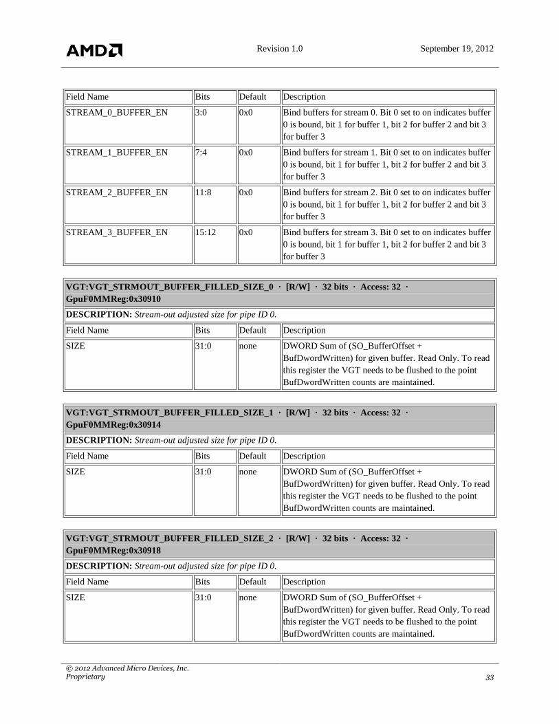
VGT:VGT_STRMOUT_BUFFER_CONFIG · [R/W] · 32 bits · Access: 32 · GpuF0MMReg:0x28b98
DESCRIPTION: Stream out enable bits. CP will use for SO coherency register validness.
Revision 1.0 September 19, 2012
© 2012 Advanced Micro Devices, Inc. Proprietary 33
Field Name Bits Default Description
STREAM_0_BUFFER_EN 3:0 0x0 Bind buffers for stream 0. Bit 0 set to on indicates buffer
0 is bound, bit 1 for buffer 1, bit 2 for buffer 2 and bit 3
for buffer 3
STREAM_1_BUFFER_EN 7:4 0x0 Bind buffers for stream 1. Bit 0 set to on indicates buffer
0 is bound, bit 1 for buffer 1, bit 2 for buffer 2 and bit 3
for buffer 3
STREAM_2_BUFFER_EN 11:8 0x0 Bind buffers for stream 2. Bit 0 set to on indicates buffer
0 is bound, bit 1 for buffer 1, bit 2 for buffer 2 and bit 3
for buffer 3
STREAM_3_BUFFER_EN 15:12 0x0 Bind buffers for stream 3. Bit 0 set to on indicates buffer
0 is bound, bit 1 for buffer 1, bit 2 for buffer 2 and bit 3
for buffer 3
VGT:VGT_STRMOUT_BUFFER_FILLED_SIZE_0 · [R/W] · 32 bits · Access: 32 ·
GpuF0MMReg:0x30910
DESCRIPTION: Stream-out adjusted size for pipe ID 0.
Field Name Bits Default Description
SIZE 31:0 none DWORD Sum of (SO_BufferOffset +
BufDwordWritten) for given buffer. Read Only. To read
this register the VGT needs to be flushed to the point
BufDwordWritten counts are maintained.
VGT:VGT_STRMOUT_BUFFER_FILLED_SIZE_1 · [R/W] · 32 bits · Access: 32 ·
GpuF0MMReg:0x30914
DESCRIPTION: Stream-out adjusted size for pipe ID 0.
Field Name Bits Default Description
SIZE 31:0 none DWORD Sum of (SO_BufferOffset +
BufDwordWritten) for given buffer. Read Only. To read
this register the VGT needs to be flushed to the point
BufDwordWritten counts are maintained.
VGT:VGT_STRMOUT_BUFFER_FILLED_SIZE_2 · [R/W] · 32 bits · Access: 32 ·
GpuF0MMReg:0x30918
DESCRIPTION: Stream-out adjusted size for pipe ID 0.
Field Name Bits Default Description
SIZE 31:0 none DWORD Sum of (SO_BufferOffset +
BufDwordWritten) for given buffer. Read Only. To read
this register the VGT needs to be flushed to the point
BufDwordWritten counts are maintained.

Revision 1.0 September 19, 2012
© 2012 Advanced Micro Devices, Inc. Proprietary 34
VGT:VGT_STRMOUT_BUFFER_FILLED_SIZE_3 · [R/W] · 32 bits · Access: 32 ·
GpuF0MMReg:0x3091c
DESCRIPTION: Stream-out adjusted size for pipe ID 0.
Field Name Bits Default Description
SIZE 31:0 none DWORD Sum of (SO_BufferOffset +
BufDwordWritten) for given buffer. Read Only. To read
this register the VGT needs to be flushed to the point
BufDwordWritten counts are maintained.
VGT:VGT_STRMOUT_BUFFER_OFFSET_0 · [R/W] · 32 bits · Access: 32 · GpuF0MMReg:0x28adc
DESCRIPTION: Stream out offset.
Field Name Bits Default Description
OFFSET 31:0 none DWORD offset for given stream out buffer. Writing this
register will cause the VGT to load a Zero into
BufDwordWritten[4] and SO_CurVertIndex.
VGT:VGT_STRMOUT_BUFFER_OFFSET_1 · [R/W] · 32 bits · Access: 32 · GpuF0MMReg:0x28aec
DESCRIPTION: Stream out offset.
Field Name Bits Default Description
OFFSET 31:0 none DWORD offset for given stream out buffer. Writing this
register will cause the VGT to load a Zero into
BufDwordWritten[4] and SO_CurVertIndex.
VGT:VGT_STRMOUT_BUFFER_OFFSET_2 · [R/W] · 32 bits · Access: 32 · GpuF0MMReg:0x28afc
DESCRIPTION: Stream out offset.
Field Name Bits Default Description
OFFSET 31:0 none DWORD offset for given stream out buffer. Writing this
register will cause the VGT to load a Zero into
BufDwordWritten[4] and SO_CurVertIndex.
VGT:VGT_STRMOUT_BUFFER_OFFSET_3 · [R/W] · 32 bits · Access: 32 · GpuF0MMReg:0x28b0c
DESCRIPTION: Stream out offset.
Field Name Bits Default Description
OFFSET 31:0 none DWORD offset for given stream out buffer. Writing this
register will cause the VGT to load a Zero into
BufDwordWritten[4] and SO_CurVertIndex.
VGT:VGT_STRMOUT_BUFFER_SIZE_0 · [R/W] · 32 bits · Access: 32 · GpuF0MMReg:0x28ad0
DESCRIPTION: Stream-out size.

Revision 1.0 September 19, 2012
© 2012 Advanced Micro Devices, Inc. Proprietary 35
Field Name Bits Default Description
SIZE 31:0 none DWORD Buffer size for given stream out buffer.
VGT:VGT_STRMOUT_BUFFER_SIZE_1 · [R/W] · 32 bits · Access: 32 · GpuF0MMReg:0x28ae0
DESCRIPTION: Stream-out size.
Field Name Bits Default Description
SIZE 31:0 none DWORD Buffer size for given stream out buffer.
VGT:VGT_STRMOUT_BUFFER_SIZE_2 · [R/W] · 32 bits · Access: 32 · GpuF0MMReg:0x28af0
DESCRIPTION: Stream-out size.
Field Name Bits Default Description
SIZE 31:0 none DWORD Buffer size for given stream out buffer.
VGT:VGT_STRMOUT_BUFFER_SIZE_3 · [R/W] · 32 bits · Access: 32 · GpuF0MMReg:0x28b00
DESCRIPTION: Stream-out size.
Field Name Bits Default Description
SIZE 31:0 none DWORD Buffer size for given stream out buffer.
VGT:VGT_STRMOUT_CONFIG · [R/W] · 32 bits · Access: 32 · GpuF0MMReg:0x28b94
DESCRIPTION: This register enables streaming out
Field Name Bits Default Description
STREAMOUT_0_EN 0 0x0 If set, stream output to stream 0 is enabled
STREAMOUT_1_EN 1 0x0 If set, stream output to stream 1 is enabled
STREAMOUT_2_EN 2 0x0 If set, stream output to stream 2 is enabled
STREAMOUT_3_EN 3 0x0 If set, stream output to stream 3 is enabled
RAST_STREAM 6:4 0x0 Stream for which rasterization is enabled, If bit[6] is set
then rasterization is not enabled for any stream
RAST_STREAM_MASK 11:8 0x0 Mask indicating which stream is enabled. Only valid if
USE_RAST_STREAM_MASK is 1
USE_RAST_STREAM_MASK 31 0x0 RAST_STREAM_MASK is used when 1. When 0
RAST_STREAM is used
VGT:VGT_STRMOUT_DRAW_OPAQUE_BUFFER_FILLED_SIZE · [R/W] · 32 bits · Access: 32 ·
GpuF0MMReg:0x28b2c
DESCRIPTION: Draw opaque size.
Field Name Bits Default Description
SIZE 31:0 none This will be loaded by the CP for a DrawOpaque call by

Revision 1.0 September 19, 2012
© 2012 Advanced Micro Devices, Inc. Proprietary 36
fetching a memory address containing last
bufferfilledsize associated with the previous stream out
buffer bound to the IA.
VGT:VGT_STRMOUT_DRAW_OPAQUE_OFFSET · [R/W] · 32 bits · Access: 32 ·
GpuF0MMReg:0x28b28
DESCRIPTION: Draw opaque offset.
Field Name Bits Default Description
OFFSET 31:0 none pOffsets from the IASetVertexBuffers binding of a
stream out buffer that is to be used as src data. The
retrived BufferFilledSize minus this poffset if positive,
will determine the amount of data from which primitives
can be created.
VGT:VGT_STRMOUT_DRAW_OPAQUE_VERTEX_STRIDE · [R/W] · 32 bits · Access: 32 ·
GpuF0MMReg:0x28b30
DESCRIPTION: Draw opaque vertex stride.
Field Name Bits Default Description
VERTEX_STRIDE 8:0 none vertex stride used for draw opaque call
VGT:VGT_STRMOUT_VTX_STRIDE_0 · [R/W] · 32 bits · Access: 32 · GpuF0MMReg:0x28ad4
DESCRIPTION: Stream out stride.
Field Name Bits Default Description
STRIDE 9:0 none DWORD stride between vertices in given stream-out
buffer. From stream output declarations details of dx10
spec, the max stride 2048 bytes or 512 words defined to
be the spacing between the beginning of each vertex.
VGT:VGT_STRMOUT_VTX_STRIDE_1 · [R/W] · 32 bits · Access: 32 · GpuF0MMReg:0x28ae4
DESCRIPTION: Stream out stride.
Field Name Bits Default Description
STRIDE 9:0 none DWORD stride between vertices in given stream-out
buffer. From stream output declarations details of dx10
spec, the max stride 2048 bytes or 512 words defined to
be the spacing between the beginning of each vertex.
VGT:VGT_STRMOUT_VTX_STRIDE_2 · [R/W] · 32 bits · Access: 32 · GpuF0MMReg:0x28af4
DESCRIPTION: Stream out stride.
Field Name Bits Default Description

Revision 1.0 September 19, 2012
© 2012 Advanced Micro Devices, Inc. Proprietary 37
STRIDE 9:0 none DWORD stride between vertices in given stream-out
buffer. From stream output declarations details of dx10
spec, the max stride 2048 bytes or 512 words defined to
be the spacing between the beginning of each vertex.
VGT:VGT_STRMOUT_VTX_STRIDE_3 · [R/W] · 32 bits · Access: 32 · GpuF0MMReg:0x28b04
DESCRIPTION: Stream out stride.
Field Name Bits Default Description
STRIDE 9:0 none DWORD stride between vertices in given stream-out
buffer. From stream output declarations details of dx10
spec, the max stride 2048 bytes or 512 words defined to
be the spacing between the beginning of each vertex.
VGT:VGT_TF_MEMORY_BASE · [R/W] · 32 bits · Access: 32 · GpuF0MMReg:0x30940
DESCRIPTION: Base address for the Tessellation Factor Memory
Field Name Bits Default Description
BASE 31:0 0x0 Base address for the Tessellation Factor Memory. 256
byte aligned. [39:8]
VGT:VGT_TF_PARAM · [R/W] · 32 bits · Access: 32 · GpuF0MMReg:0x28b6c
DESCRIPTION: Used to specify tessellation engine control parameters
Field Name Bits Default Description
TYPE 1:0 none Tessellation type (domain) used
POSSIBLE VALUES:
00 - TESS_ISOLINE
01 - TESS_TRIANGLE
02 - TESS_QUAD
PARTITIONING 4:2 none Partition type used
POSSIBLE VALUES:
00 - PART_INTEGER
01 - PART_POW2
02 - PART_FRAC_ODD
03 - PART_FRAC_EVEN
TOPOLOGY 7:5 none Output primitive topology
POSSIBLE VALUES:
00 - OUTPUT_POINT
01 - OUTPUT_LINE
02 - OUTPUT_TRIANGLE_CW
03 - OUTPUT_TRIANGLE_CCW
NUM_DS_WAVES_PER_SIMD 13:10 none How many DS waves (ES/VS) are sent to the same SIMD
before spilling to other SIMDs to use the offchip LDS
data
DISABLE_DONUTS 14 none Determines which walking pattern is used in the Dx11
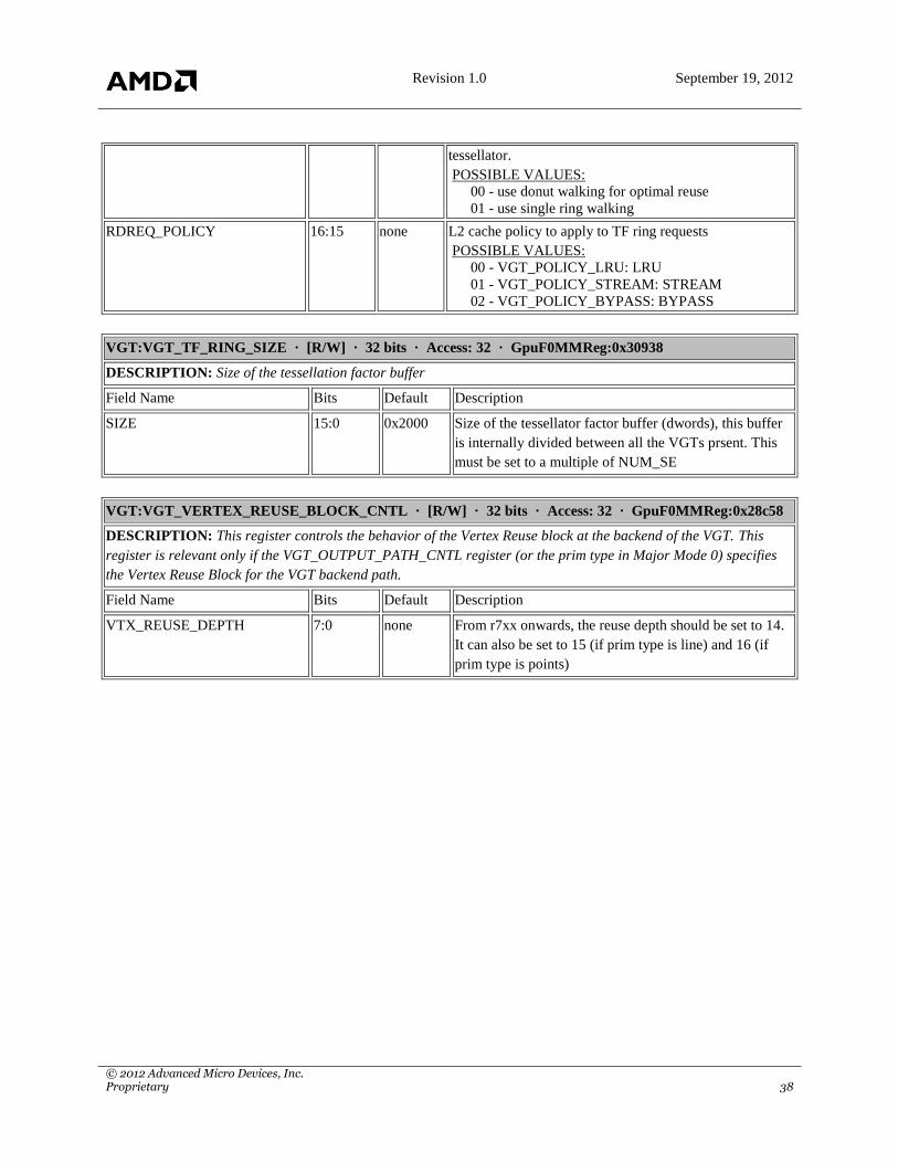
Revision 1.0 September 19, 2012
© 2012 Advanced Micro Devices, Inc. Proprietary 38
tessellator.
POSSIBLE VALUES:
00 - use donut walking for optimal reuse
01 - use single ring walking
RDREQ_POLICY 16:15 none L2 cache policy to apply to TF ring requests
POSSIBLE VALUES:
00 - VGT_POLICY_LRU: LRU
01 - VGT_POLICY_STREAM: STREAM
02 - VGT_POLICY_BYPASS: BYPASS
VGT:VGT_TF_RING_SIZE · [R/W] · 32 bits · Access: 32 · GpuF0MMReg:0x30938
DESCRIPTION: Size of the tessellation factor buffer
Field Name Bits Default Description
SIZE 15:0 0x2000 Size of the tessellator factor buffer (dwords), this buffer
is internally divided between all the VGTs prsent. This
must be set to a multiple of NUM_SE
VGT:VGT_VERTEX_REUSE_BLOCK_CNTL · [R/W] · 32 bits · Access: 32 · GpuF0MMReg:0x28c58
DESCRIPTION: This register controls the behavior of the Vertex Reuse block at the backend of the VGT. This
register is relevant only if the VGT_OUTPUT_PATH_CNTL register (or the prim type in Major Mode 0) specifies
the Vertex Reuse Block for the VGT backend path.
Field Name Bits Default Description
VTX_REUSE_DEPTH 7:0 none From r7xx onwards, the reuse depth should be set to 14.
It can also be set to 15 (if prim type is line) and 16 (if
prim type is points)

Revision 1.0 September 19, 2012
© 2012 Advanced Micro Devices, Inc. Proprietary 39
2. Primitive Assembly Registers
PA:PA_CL_CLIP_CNTL · [R/W] · 32 bits · Access: 32 · GpuF0MMReg:0x28810
DESCRIPTION: Clipper Control Bits
Field Name Bits Default Description
UCP_ENA_0 0 none Enable User-Clip Plane 0
UCP_ENA_1 1 none Enable User-Clip Plane 1
UCP_ENA_2 2 none Enable User-Clip Plane 2
UCP_ENA_3 3 none Enable User-Clip Plane 3
UCP_ENA_4 4 none Enable User-Clip Plane 4
UCP_ENA_5 5 none Enable User-Clip Plane 5
PS_UCP_Y_SCALE_NEG 13 none
PS_UCP_MODE 15:14 none 0 = Cull using distance from center of point
1 = Cull using radius-based distance from center of
point
2 = Cull using radius-based distance from center of
point, Expand and Clip on intersection
3 = Always expand and clip as trifan
CLIP_DISABLE 16 none Disables clip code generation and clipping process for
TCL
UCP_CULL_ONLY_ENA 17 none Cull Primitives against UCPS, but don`t clip
BOUNDARY_EDGE_FLAG_ENA 18 none Currently unused: Pending Delete. Left as placeholder
for now.
DX_CLIP_SPACE_DEF 19 none Clip space is defined as:
0: -W < X < W, -W < Y < W, -W < Z < W (OpenGL
Definition)
1: -W < X < W, -W < Y < W, 0 < Z < W (DirectX
Definition)
DIS_CLIP_ERR_DETECT 20 none Disables culling of primitives for which the clipped
detects an error. Default is 0
VTX_KILL_OR 21 none Used if Vertex Kill flags are exported from Vertex
Shader. If clear, ALL vertices for current primitive
must be set to kill the primitive (AND MODE). If set,
if ANY vertices for current primitive are set, the
primitive will be killed (OR MODE).
DX_RASTERIZATION_KILL 22 none
DX_LINEAR_ATTR_CLIP_ENA 24 none
VTE_VPORT_PROVOKE_DISABLE 25 none
ZCLIP_NEAR_DISABLE 26 none
ZCLIP_FAR_DISABLE 27 none
PA:PA_CL_CNTL_STATUS · [R] · 32 bits · Access: 32 · GpuF0MMReg:0x8a10

Revision 1.0 September 19, 2012
© 2012 Advanced Micro Devices, Inc. Proprietary 40
DESCRIPTION: Status Bits
Field Name Bits Default Description
CL_BUSY 31 none Busy Status Bit
PA:PA_CL_ENHANCE · [R/W] · 32 bits · Access: 32 · GpuF0MMReg:0x8a14
DESCRIPTION: Used for Late Additions of Control Bits
Field Name Bits Default Description
CLIP_VTX_REORDER_ENA 0 0x1 Enables vertex-order-independent clipping
NUM_CLIP_SEQ 2:1 0x3 Number of Clip Sequences Active (+1). Should be set to
3 (4 sequences) for best performance
CLIPPED_PRIM_SEQ_STALL 3 none Forces a faster clip path if NUM_CLIP_SEQ is set to 0
(which should only be if 3 does not work)
VE_NAN_PROC_DISABLE 4 none
PA:PA_CL_GB_HORZ_CLIP_ADJ · [R/W] · 32 bits · Access: 32 · GpuF0MMReg:0x28bf0
DESCRIPTION: Horizontal Guard Band Clip Adjust Register
Field Name Bits Default Description
DATA_REGISTER 31:0 none 32-bit floating point value. Should be set to 1.0 for no
guard band.
PA:PA_CL_GB_HORZ_DISC_ADJ · [R/W] · 32 bits · Access: 32 · GpuF0MMReg:0x28bf4
DESCRIPTION: Horizontal Guard Band Discard Adjust Register
Field Name Bits Default Description
DATA_REGISTER 31:0 none 32-bit floating point value. Should be set to 1.0 for no
guard band.
PA:PA_CL_GB_VERT_CLIP_ADJ · [R/W] · 32 bits · Access: 32 · GpuF0MMReg:0x28be8
DESCRIPTION: Vertical Guard Band Clip Adjust Register
Field Name Bits Default Description
DATA_REGISTER 31:0 none 32-bit floating point value. Should be set to 1.0 for no
guard band.
PA:PA_CL_GB_VERT_DISC_ADJ · [R/W] · 32 bits · Access: 32 · GpuF0MMReg:0x28bec
DESCRIPTION: Vertical Guard Band Discard Adjust Register
Field Name Bits Default Description
DATA_REGISTER 31:0 none 32-bit floating point value. Should be set to 1.0 for no
guard band.
PA:PA_CL_NANINF_CNTL · [R/W] · 32 bits · Access: 32 · GpuF0MMReg:0x28820
Field Name Bits Default Description
VTE_XY_INF_DISCARD 0 none
VTE_Z_INF_DISCARD 1 none

Revision 1.0 September 19, 2012
© 2012 Advanced Micro Devices, Inc. Proprietary 41
VTE_W_INF_DISCARD 2 none
VTE_0XNANINF_IS_0 3 none
VTE_XY_NAN_RETAIN 4 none
VTE_Z_NAN_RETAIN 5 none
VTE_W_NAN_RETAIN 6 none
VTE_W_RECIP_NAN_IS_0 7 none
VS_XY_NAN_TO_INF 8 none
VS_XY_INF_RETAIN 9 none
VS_Z_NAN_TO_INF 10 none
VS_Z_INF_RETAIN 11 none
VS_W_NAN_TO_INF 12 none
VS_W_INF_RETAIN 13 none
VS_CLIP_DIST_INF_DISCARD 14 none
VTE_NO_OUTPUT_NEG_0 20 none
PA:PA_CL_POINT_CULL_RAD · [R/W] · 32 bits · Access: 32 · GpuF0MMReg:0x287e0
DESCRIPTION: Point Sprite Culling Radius Expansion SQRT(XRadExp^2 + YRadExp^2)
Field Name Bits Default Description
DATA_REGISTER 31:0 none
PA:PA_CL_POINT_SIZE · [R/W] · 32 bits · Access: 32 · GpuF0MMReg:0x287dc
DESCRIPTION: Point Sprite Constant Size
Field Name Bits Default Description
DATA_REGISTER 31:0 none
PA:PA_CL_POINT_X_RAD · [R/W] · 32 bits · Access: 32 · GpuF0MMReg:0x287d4
DESCRIPTION: Point Sprite X Radius Expansion
Field Name Bits Default Description
DATA_REGISTER 31:0 none
PA:PA_CL_POINT_Y_RAD · [R/W] · 32 bits · Access: 32 · GpuF0MMReg:0x287d8
DESCRIPTION: Point Sprite Y Radius Expansion
Field Name Bits Default Description
DATA_REGISTER 31:0 none
PA:PA_CL_UCP_[0-5]_W · [R/W] · 32 bits · Access: 32 · GpuF0MMReg:0x285c8-0x28618
DESCRIPTION: User Clip Plane Data
Field Name Bits Default Description
DATA_REGISTER 31:0 none
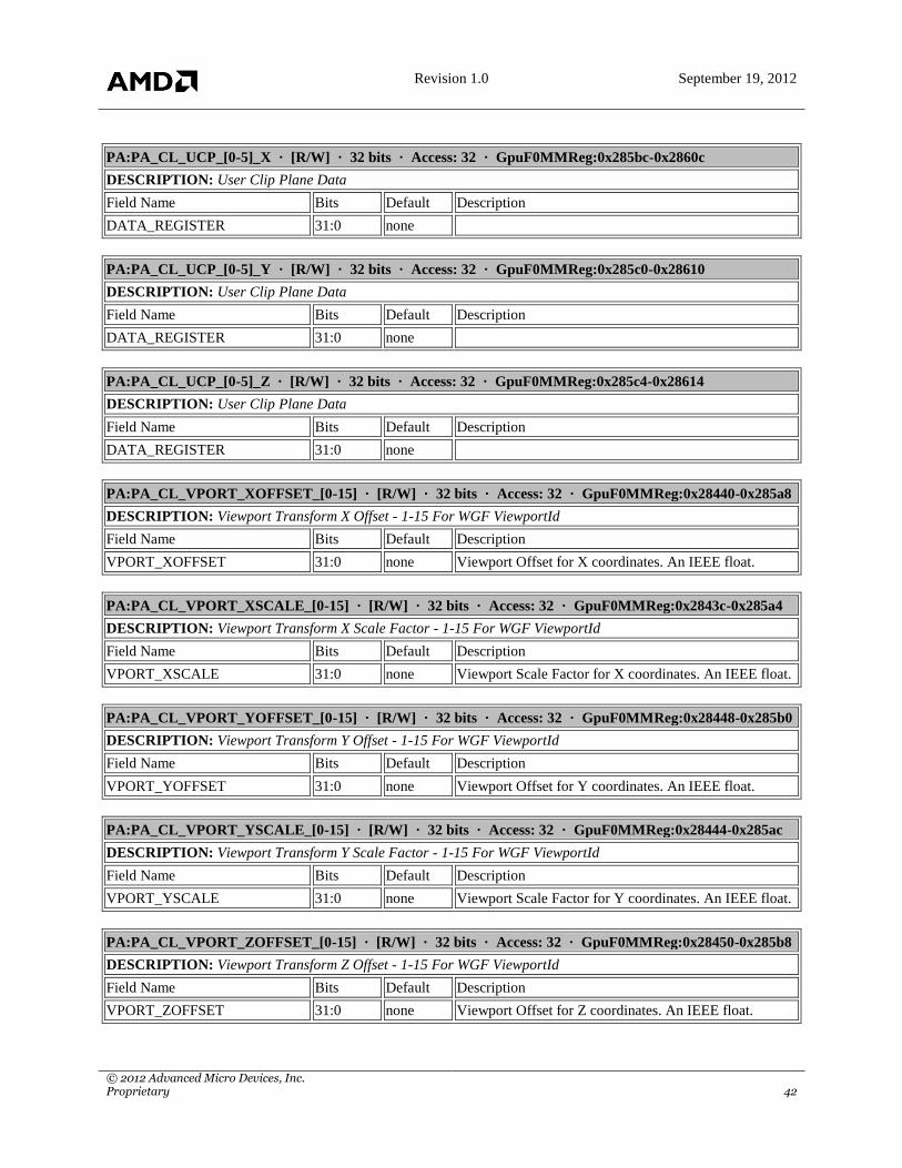
Revision 1.0 September 19, 2012
© 2012 Advanced Micro Devices, Inc. Proprietary 42
PA:PA_CL_UCP_[0-5]_X · [R/W] · 32 bits · Access: 32 · GpuF0MMReg:0x285bc-0x2860c
DESCRIPTION: User Clip Plane Data
Field Name Bits Default Description
DATA_REGISTER 31:0 none
PA:PA_CL_UCP_[0-5]_Y · [R/W] · 32 bits · Access: 32 · GpuF0MMReg:0x285c0-0x28610
DESCRIPTION: User Clip Plane Data
Field Name Bits Default Description
DATA_REGISTER 31:0 none
PA:PA_CL_UCP_[0-5]_Z · [R/W] · 32 bits · Access: 32 · GpuF0MMReg:0x285c4-0x28614
DESCRIPTION: User Clip Plane Data
Field Name Bits Default Description
DATA_REGISTER 31:0 none
PA:PA_CL_VPORT_XOFFSET_[0-15] · [R/W] · 32 bits · Access: 32 · GpuF0MMReg:0x28440-0x285a8
DESCRIPTION: Viewport Transform X Offset - 1-15 For WGF ViewportId
Field Name Bits Default Description
VPORT_XOFFSET 31:0 none Viewport Offset for X coordinates. An IEEE float.
PA:PA_CL_VPORT_XSCALE_[0-15] · [R/W] · 32 bits · Access: 32 · GpuF0MMReg:0x2843c-0x285a4
DESCRIPTION: Viewport Transform X Scale Factor - 1-15 For WGF ViewportId
Field Name Bits Default Description
VPORT_XSCALE 31:0 none Viewport Scale Factor for X coordinates. An IEEE float.
PA:PA_CL_VPORT_YOFFSET_[0-15] · [R/W] · 32 bits · Access: 32 · GpuF0MMReg:0x28448-0x285b0
DESCRIPTION: Viewport Transform Y Offset - 1-15 For WGF ViewportId
Field Name Bits Default Description
VPORT_YOFFSET 31:0 none Viewport Offset for Y coordinates. An IEEE float.
PA:PA_CL_VPORT_YSCALE_[0-15] · [R/W] · 32 bits · Access: 32 · GpuF0MMReg:0x28444-0x285ac
DESCRIPTION: Viewport Transform Y Scale Factor - 1-15 For WGF ViewportId
Field Name Bits Default Description
VPORT_YSCALE 31:0 none Viewport Scale Factor for Y coordinates. An IEEE float.
PA:PA_CL_VPORT_ZOFFSET_[0-15] · [R/W] · 32 bits · Access: 32 · GpuF0MMReg:0x28450-0x285b8
DESCRIPTION: Viewport Transform Z Offset - 1-15 For WGF ViewportId
Field Name Bits Default Description
VPORT_ZOFFSET 31:0 none Viewport Offset for Z coordinates. An IEEE float.

Revision 1.0 September 19, 2012
© 2012 Advanced Micro Devices, Inc. Proprietary 43
PA:PA_CL_VPORT_ZSCALE_[0-15] · [R/W] · 32 bits · Access: 32 · GpuF0MMReg:0x2844c-0x285b4
DESCRIPTION: Viewport Transform Z Scale Factor - 1-15 For WGF ViewportId
Field Name Bits Default Description
VPORT_ZSCALE 31:0 none Viewport Scale Factor for Z coordinates. An IEEE float.
PA:PA_CL_VS_OUT_CNTL · [R/W] · 32 bits · Access: 32 · GpuF0MMReg:0x2881c
DESCRIPTION: Vertex Shader Output Control
Field Name Bits Default Description
CLIP_DIST_ENA_0 0 none Enable ClipDistance# to be used for user-defined
clipping. Requires VS_OUT_CCDIST#_ENA to be
set.
CLIP_DIST_ENA_1 1 none Enable ClipDistance# to be used for user-defined
clipping. Requires VS_OUT_CCDIST#_ENA to be
set.
CLIP_DIST_ENA_2 2 none Enable ClipDistance# to be used for user-defined
clipping. Requires VS_OUT_CCDIST#_ENA to be
set.
CLIP_DIST_ENA_3 3 none Enable ClipDistance# to be used for user-defined
clipping. Requires VS_OUT_CCDIST#_ENA to be
set.
CLIP_DIST_ENA_4 4 none Enable ClipDistance# to be used for user-defined
clipping. Requires VS_OUT_CCDIST#_ENA to be
set.
CLIP_DIST_ENA_5 5 none Enable ClipDistance# to be used for user-defined
clipping. Requires VS_OUT_CCDIST#_ENA to be
set.
CLIP_DIST_ENA_6 6 none Enable ClipDistance# to be used for user-defined
clipping. Requires VS_OUT_CCDIST#_ENA to be
set.
CLIP_DIST_ENA_7 7 none Enable ClipDistance# to be used for user-defined
clipping. Requires VS_OUT_CCDIST#_ENA to be
set.
CULL_DIST_ENA_0 8 none Enable CullDistance# to be used for user-defined clip
discard. Requires VS_OUT_CCDIST#_ENA to be set.
If all verts of a primitive are outside (culldist<0), then
primitive is discarded, else just let through (i.e. NOT
clipped).
CULL_DIST_ENA_1 9 none Enable CullDistance# to be used for user-defined clip
discard. Requires VS_OUT_CCDIST#_ENA to be set.
If all verts of a primitive are outside (culldist<0), then
primitive is discarded, else just let through (i.e. NOT
clipped).
CULL_DIST_ENA_2 10 none Enable CullDistance# to be used for user-defined clip
discard. Requires VS_OUT_CCDIST#_ENA to be set.
If all verts of a primitive are outside (culldist<0), then
primitive is discarded, else just let through (i.e. NOT
clipped).

Revision 1.0 September 19, 2012
© 2012 Advanced Micro Devices, Inc. Proprietary 44
CULL_DIST_ENA_3 11 none Enable CullDistance# to be used for user-defined clip
discard. Requires VS_OUT_CCDIST#_ENA to be set.
If all verts of a primitive are outside (culldist<0), then
primitive is discarded, else just let through (i.e. NOT
clipped).
CULL_DIST_ENA_4 12 none Enable CullDistance# to be used for user-defined clip
discard. Requires VS_OUT_CCDIST#_ENA to be set.
If all verts of a primitive are outside (culldist<0), then
primitive is discarded, else just let through (i.e. NOT
clipped).
CULL_DIST_ENA_5 13 none Enable CullDistance# to be used for user-defined clip
discard. Requires VS_OUT_CCDIST#_ENA to be set.
If all verts of a primitive are outside (culldist<0), then
primitive is discarded, else just let through (i.e. NOT
clipped).
CULL_DIST_ENA_6 14 none Enable CullDistance# to be used for user-defined clip
discard. Requires VS_OUT_CCDIST#_ENA to be set.
If all verts of a primitive are outside (culldist<0), then
primitive is discarded, else just let through (i.e. NOT
clipped).
CULL_DIST_ENA_7 15 none Enable CullDistance# to be used for user-defined clip
discard. Requires VS_OUT_CCDIST#_ENA to be set.
If all verts of a primitive are outside (culldist<0), then
primitive is discarded, else just let through (i.e. NOT
clipped).
USE_VTX_POINT_SIZE 16 none Use the PointSize output from the VS (in the x channel
of VS_OUT_MISC_VEC).
USE_VTX_EDGE_FLAG 17 none Use the EdgeFlag output from the VS (in the y channel
of VS_OUT_MISC_VEC).
USE_VTX_RENDER_TARGET_INDX 18 none Use the RenderTargetArrayIndx output from the VS
(in the z channel of VS_OUT_MISC_VEC). Only
valid for WGF Geometry Shader
USE_VTX_VIEWPORT_INDX 19 none Use the ViewportArrayIndx output from the VS (in the
w channel of VS_OUT_MISC_VEC). Only valid for
WGF Geometry Shader
USE_VTX_KILL_FLAG 20 none Use the KillFlag output from the VS (in the z channel
of VS_OUT_MISC_VEC). Mutually exclusive from
RTarrayindx
VS_OUT_MISC_VEC_ENA 21 none Output the VS output misc vector from the VS (SX) to
the PA (primitive assembler). Should be set if any of
the fields are to be used
VS_OUT_CCDIST0_VEC_ENA 22 none Output the VS output ccdist0 vector from the VS (SX)
to the PA (primitive assembler). Should be set if any of
the fields are to be used
VS_OUT_CCDIST1_VEC_ENA 23 none Output the VS output ccdist1 vector from the VS (SX)
to the PA (primitive assembler). Should be set if any of
the fields are to be used
VS_OUT_MISC_SIDE_BUS_ENA 24 none

Revision 1.0 September 19, 2012
© 2012 Advanced Micro Devices, Inc. Proprietary 45
USE_VTX_GS_CUT_FLAG 25 none
PA:PA_CL_VTE_CNTL · [R/W] · 32 bits · Access: 32 · GpuF0MMReg:0x28818
DESCRIPTION: Viewport Transform Engine Control
Field Name Bits Default Description
VPORT_X_SCALE_ENA 0 none Viewport Transform Scale Enable for X component
VPORT_X_OFFSET_ENA 1 none Viewport Transform Offset Enable for X component
VPORT_Y_SCALE_ENA 2 none Viewport Transform Scale Enable for Y component
VPORT_Y_OFFSET_ENA 3 none Viewport Transform Offset Enable for Y component
VPORT_Z_SCALE_ENA 4 none Viewport Transform Scale Enable for Z component
VPORT_Z_OFFSET_ENA 5 none Viewport Transform Offset Enable for Z component
VTX_XY_FMT 8 none Indicates that the incoming X, Y have already been
multiplied by 1/W0.
If OFF, the Setup Engine will multiply the X, Y
coordinates by 1/W0.,
VTX_Z_FMT 9 none Indicates that the incoming Z has already been multiplied
by 1/W0.
If OFF, the Setup Engine will multiply the Z coordinate
by 1/W0.
VTX_W0_FMT 10 none Indicates that the incoming W0 is not 1/W0.
If ON, the Setup Engine will perform the reciprocal to get
1/W0.
PA:PA_SC_AA_CONFIG · [R/W] · 32 bits · Access: 32 · GpuF0MMReg:0x28be0
DESCRIPTION: Multisample Antialiasing Control
Field Name Bits Default Description
MSAA_NUM_SAMPLES 2:0 none Specifies the number of samples to use for MSAA Detail
Sampling. 0 = 1-sample, 1 = 2-sample, 2 = 4-sample, 3 =
8-sample, 4 = 16-sample.
AA_MASK_CENTROID_DTMN 4 none Specifies whether to apply the MSAA Mask before or
after the centroid determination. 0 = before; 1 = after.
MAX_SAMPLE_DIST 16:13 none Specifies the maximum distance (in subpixels) between
the pixel center and the outermost subpixel sample. This
value is used to optimize coarse walk and quad identity.
Should be set to 0 when not anti-aliasing. Max value for
R600 should be 8(16ths).
MSAA_EXPOSED_SAMPLES 22:20 none Specifies the number of samples the pixel shader can see
from the primitive`s coverage in the pixel. Uses the same
LOG2 encoding as MSAA_NUM_SAMPLES.
DETAIL_TO_EXPOSED_MODE 25:24 none Specifies the mode to use when converting from a higher
detail sample mask to a lower exposed mask.
0: MASK off higher samples. If result is empty, then OR
upper bits down into lower samples
1: off higher samples
2: OR higher samples down into lower samples.

Revision 1.0 September 19, 2012
© 2012 Advanced Micro Devices, Inc. Proprietary 46
PA:PA_SC_AA_MASK_X0Y0_X1Y0 · [R/W] · 32 bits · Access: 32 · GpuF0MMReg:0x28c38
DESCRIPTION: Multisample AA Mask Pixel X0,Y0 (Upper Left) and X1,Y0 (Upper Right) of Quad. If not all ones,
fully covered optimizations are disabled. Should be replicated up from the requested sample count to fill in all 16
bits per pixel.
Field Name Bits Default Description
AA_MASK_X0Y0 15:0 none 16-bit mask applied to pixel X0,Y0(ULC) as follows:
LSB is Sample0, MSB is Sample15.
AA_MASK_X1Y0 31:16 none 16-bit mask applied to pixel X1,Y0(URC) as follows:
LSB is Sample0, MSB is Sample15.
PA:PA_SC_AA_MASK_X0Y1_X1Y1 · [R/W] · 32 bits · Access: 32 · GpuF0MMReg:0x28c3c
DESCRIPTION: Multisample AA Mask Pixel X0,Y1 (Lower Left) and X1,Y1 (Lower Right) of Quad. If not all ones,
fully covered optimizations are disabled. Should be replicated up from the requested sample count to fill in all 16
bits per pixel.
Field Name Bits Default Description
AA_MASK_X0Y1 15:0 none 16-bit mask applied to pixel X0,Y1(LLC) as follows:
LSB is Sample0, MSB is Sample15.
AA_MASK_X1Y1 31:16 none 16-bit mask applied to pixel X1,Y1(LRC) as follows:
LSB is Sample0, MSB is Sample15.
PA:PA_SC_AA_SAMPLE_LOCS_PIXEL_X0Y0_0 · [R/W] · 32 bits · Access: 32 ·
GpuF0MMReg:0x28bf8
DESCRIPTION: Multi-Sample Programmable Sample Locations 0-3 for Pixel X0,Y0 (Upper Left) of Quad - Used
by SC, SPI, DB, CB
Field Name Bits Default Description
S0_X 3:0 none 4b signed offset from pixel center. Range -8/16 to 7/16.
S0_Y 7:4 none 4b signed offset from pixel center. Range -8/16 to 7/16.
S1_X 11:8 none 4b signed offset from pixel center. Range -8/16 to 7/16.
S1_Y 15:12 none 4b signed offset from pixel center. Range -8/16 to 7/16.
S2_X 19:16 none 4b signed offset from pixel center. Range -8/16 to 7/16.
S2_Y 23:20 none 4b signed offset from pixel center. Range -8/16 to 7/16.
S3_X 27:24 none 4b signed offset from pixel center. Range -8/16 to 7/16.
S3_Y 31:28 none 4b signed offset from pixel center. Range -8/16 to 7/16.
PA:PA_SC_AA_SAMPLE_LOCS_PIXEL_X0Y0_1 · [R/W] · 32 bits · Access: 32 ·
GpuF0MMReg:0x28bfc
DESCRIPTION: Multi-Sample Programmable Sample Locations 4-7 for Pixel X0,Y0 (Upper Left) of Quad - Used
by SC, SPI, DB, CB
Field Name Bits Default Description
S4_X 3:0 none 4b signed offset from pixel center. Range -8/16 to 7/16.
S4_Y 7:4 none 4b signed offset from pixel center. Range -8/16 to 7/16.
S5_X 11:8 none 4b signed offset from pixel center. Range -8/16 to 7/16.
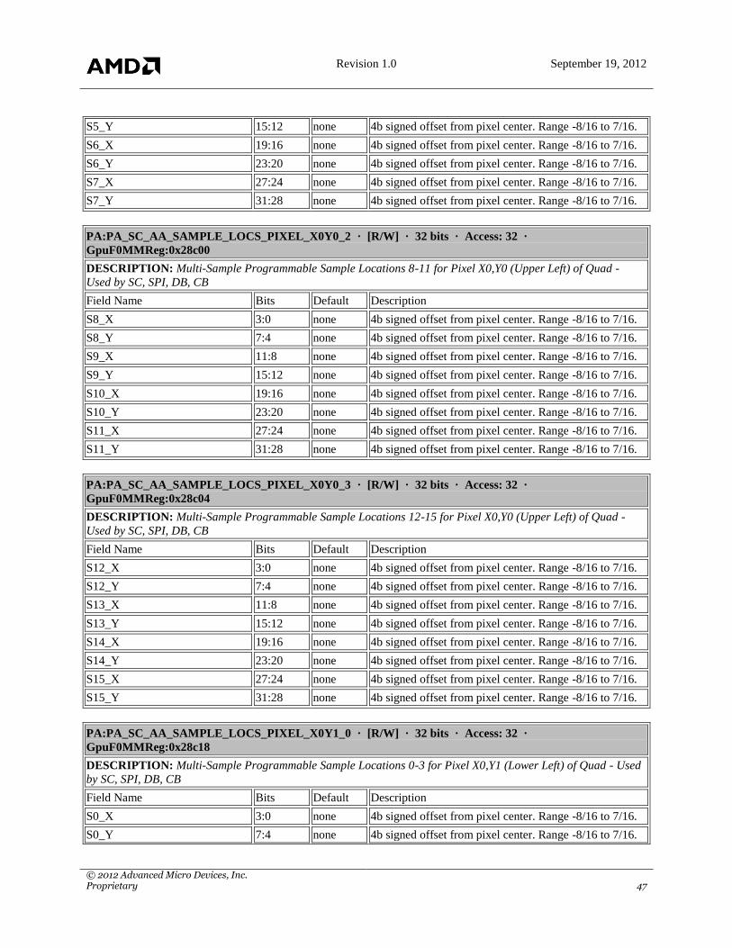
Revision 1.0 September 19, 2012
© 2012 Advanced Micro Devices, Inc. Proprietary 47
S5_Y 15:12 none 4b signed offset from pixel center. Range -8/16 to 7/16.
S6_X 19:16 none 4b signed offset from pixel center. Range -8/16 to 7/16.
S6_Y 23:20 none 4b signed offset from pixel center. Range -8/16 to 7/16.
S7_X 27:24 none 4b signed offset from pixel center. Range -8/16 to 7/16.
S7_Y 31:28 none 4b signed offset from pixel center. Range -8/16 to 7/16.
PA:PA_SC_AA_SAMPLE_LOCS_PIXEL_X0Y0_2 · [R/W] · 32 bits · Access: 32 ·
GpuF0MMReg:0x28c00
DESCRIPTION: Multi-Sample Programmable Sample Locations 8-11 for Pixel X0,Y0 (Upper Left) of Quad -
Used by SC, SPI, DB, CB
Field Name Bits Default Description
S8_X 3:0 none 4b signed offset from pixel center. Range -8/16 to 7/16.
S8_Y 7:4 none 4b signed offset from pixel center. Range -8/16 to 7/16.
S9_X 11:8 none 4b signed offset from pixel center. Range -8/16 to 7/16.
S9_Y 15:12 none 4b signed offset from pixel center. Range -8/16 to 7/16.
S10_X 19:16 none 4b signed offset from pixel center. Range -8/16 to 7/16.
S10_Y 23:20 none 4b signed offset from pixel center. Range -8/16 to 7/16.
S11_X 27:24 none 4b signed offset from pixel center. Range -8/16 to 7/16.
S11_Y 31:28 none 4b signed offset from pixel center. Range -8/16 to 7/16.
PA:PA_SC_AA_SAMPLE_LOCS_PIXEL_X0Y0_3 · [R/W] · 32 bits · Access: 32 ·
GpuF0MMReg:0x28c04
DESCRIPTION: Multi-Sample Programmable Sample Locations 12-15 for Pixel X0,Y0 (Upper Left) of Quad -
Used by SC, SPI, DB, CB
Field Name Bits Default Description
S12_X 3:0 none 4b signed offset from pixel center. Range -8/16 to 7/16.
S12_Y 7:4 none 4b signed offset from pixel center. Range -8/16 to 7/16.
S13_X 11:8 none 4b signed offset from pixel center. Range -8/16 to 7/16.
S13_Y 15:12 none 4b signed offset from pixel center. Range -8/16 to 7/16.
S14_X 19:16 none 4b signed offset from pixel center. Range -8/16 to 7/16.
S14_Y 23:20 none 4b signed offset from pixel center. Range -8/16 to 7/16.
S15_X 27:24 none 4b signed offset from pixel center. Range -8/16 to 7/16.
S15_Y 31:28 none 4b signed offset from pixel center. Range -8/16 to 7/16.
PA:PA_SC_AA_SAMPLE_LOCS_PIXEL_X0Y1_0 · [R/W] · 32 bits · Access: 32 ·
GpuF0MMReg:0x28c18
DESCRIPTION: Multi-Sample Programmable Sample Locations 0-3 for Pixel X0,Y1 (Lower Left) of Quad - Used
by SC, SPI, DB, CB
Field Name Bits Default Description
S0_X 3:0 none 4b signed offset from pixel center. Range -8/16 to 7/16.
S0_Y 7:4 none 4b signed offset from pixel center. Range -8/16 to 7/16.

Revision 1.0 September 19, 2012
© 2012 Advanced Micro Devices, Inc. Proprietary 48
S1_X 11:8 none 4b signed offset from pixel center. Range -8/16 to 7/16.
S1_Y 15:12 none 4b signed offset from pixel center. Range -8/16 to 7/16.
S2_X 19:16 none 4b signed offset from pixel center. Range -8/16 to 7/16.
S2_Y 23:20 none 4b signed offset from pixel center. Range -8/16 to 7/16.
S3_X 27:24 none 4b signed offset from pixel center. Range -8/16 to 7/16.
S3_Y 31:28 none 4b signed offset from pixel center. Range -8/16 to 7/16.
PA:PA_SC_AA_SAMPLE_LOCS_PIXEL_X0Y1_1 · [R/W] · 32 bits · Access: 32 ·
GpuF0MMReg:0x28c1c
DESCRIPTION: Multi-Sample Programmable Sample Locations 4-7 for Pixel X0,Y1 (Lower Left) of Quad - Used
by SC, SPI, DB, CB
Field Name Bits Default Description
S4_X 3:0 none 4b signed offset from pixel center. Range -8/16 to 7/16.
S4_Y 7:4 none 4b signed offset from pixel center. Range -8/16 to 7/16.
S5_X 11:8 none 4b signed offset from pixel center. Range -8/16 to 7/16.
S5_Y 15:12 none 4b signed offset from pixel center. Range -8/16 to 7/16.
S6_X 19:16 none 4b signed offset from pixel center. Range -8/16 to 7/16.
S6_Y 23:20 none 4b signed offset from pixel center. Range -8/16 to 7/16.
S7_X 27:24 none 4b signed offset from pixel center. Range -8/16 to 7/16.
S7_Y 31:28 none 4b signed offset from pixel center. Range -8/16 to 7/16.
PA:PA_SC_AA_SAMPLE_LOCS_PIXEL_X0Y1_2 · [R/W] · 32 bits · Access: 32 ·
GpuF0MMReg:0x28c20
DESCRIPTION: Multi-Sample Programmable Sample Locations 8-11 for Pixel X0,Y1 (Lower Left) of Quad -
Used by SC, SPI, DB, CB
Field Name Bits Default Description
S8_X 3:0 none 4b signed offset from pixel center. Range -8/16 to 7/16.
S8_Y 7:4 none 4b signed offset from pixel center. Range -8/16 to 7/16.
S9_X 11:8 none 4b signed offset from pixel center. Range -8/16 to 7/16.
S9_Y 15:12 none 4b signed offset from pixel center. Range -8/16 to 7/16.
S10_X 19:16 none 4b signed offset from pixel center. Range -8/16 to 7/16.
S10_Y 23:20 none 4b signed offset from pixel center. Range -8/16 to 7/16.
S11_X 27:24 none 4b signed offset from pixel center. Range -8/16 to 7/16.
S11_Y 31:28 none 4b signed offset from pixel center. Range -8/16 to 7/16.
PA:PA_SC_AA_SAMPLE_LOCS_PIXEL_X0Y1_3 · [R/W] · 32 bits · Access: 32 ·
GpuF0MMReg:0x28c24
DESCRIPTION: Multi-Sample Programmable Sample Locations 12-15 for Pixel X0,Y1 (Lower Left) of Quad -
Used by SC, SPI, DB, CB
Field Name Bits Default Description
S12_X 3:0 none 4b signed offset from pixel center. Range -8/16 to 7/16.

Revision 1.0 September 19, 2012
© 2012 Advanced Micro Devices, Inc. Proprietary 49
S12_Y 7:4 none 4b signed offset from pixel center. Range -8/16 to 7/16.
S13_X 11:8 none 4b signed offset from pixel center. Range -8/16 to 7/16.
S13_Y 15:12 none 4b signed offset from pixel center. Range -8/16 to 7/16.
S14_X 19:16 none 4b signed offset from pixel center. Range -8/16 to 7/16.
S14_Y 23:20 none 4b signed offset from pixel center. Range -8/16 to 7/16.
S15_X 27:24 none 4b signed offset from pixel center. Range -8/16 to 7/16.
S15_Y 31:28 none 4b signed offset from pixel center. Range -8/16 to 7/16.
PA:PA_SC_AA_SAMPLE_LOCS_PIXEL_X1Y0_0 · [R/W] · 32 bits · Access: 32 ·
GpuF0MMReg:0x28c08
DESCRIPTION: Multi-Sample Programmable Sample Locations 0-3 for Pixel X1,Y0 (Upper Right) of Quad -
Used by SC, SPI, DB, CB
Field Name Bits Default Description
S0_X 3:0 none 4b signed offset from pixel center. Range -8/16 to 7/16.
S0_Y 7:4 none 4b signed offset from pixel center. Range -8/16 to 7/16.
S1_X 11:8 none 4b signed offset from pixel center. Range -8/16 to 7/16.
S1_Y 15:12 none 4b signed offset from pixel center. Range -8/16 to 7/16.
S2_X 19:16 none 4b signed offset from pixel center. Range -8/16 to 7/16.
S2_Y 23:20 none 4b signed offset from pixel center. Range -8/16 to 7/16.
S3_X 27:24 none 4b signed offset from pixel center. Range -8/16 to 7/16.
S3_Y 31:28 none 4b signed offset from pixel center. Range -8/16 to 7/16.
PA:PA_SC_AA_SAMPLE_LOCS_PIXEL_X1Y0_1 · [R/W] · 32 bits · Access: 32 ·
GpuF0MMReg:0x28c0c
DESCRIPTION: Multi-Sample Programmable Sample Locations 4-7 for Pixel X1,Y0 (Upper Right) of Quad -
Used by SC, SPI, DB, CB
Field Name Bits Default Description
S4_X 3:0 none 4b signed offset from pixel center. Range -8/16 to 7/16.
S4_Y 7:4 none 4b signed offset from pixel center. Range -8/16 to 7/16.
S5_X 11:8 none 4b signed offset from pixel center. Range -8/16 to 7/16.
S5_Y 15:12 none 4b signed offset from pixel center. Range -8/16 to 7/16.
S6_X 19:16 none 4b signed offset from pixel center. Range -8/16 to 7/16.
S6_Y 23:20 none 4b signed offset from pixel center. Range -8/16 to 7/16.
S7_X 27:24 none 4b signed offset from pixel center. Range -8/16 to 7/16.
S7_Y 31:28 none 4b signed offset from pixel center. Range -8/16 to 7/16.
PA:PA_SC_AA_SAMPLE_LOCS_PIXEL_X1Y0_2 · [R/W] · 32 bits · Access: 32 ·
GpuF0MMReg:0x28c10
DESCRIPTION: Multi-Sample Programmable Sample Locations 8-11 for Pixel X1,Y0 (Upper Right) of Quad -
Used by SC, SPI, DB, CB
Field Name Bits Default Description

Revision 1.0 September 19, 2012
© 2012 Advanced Micro Devices, Inc. Proprietary 50
S8_X 3:0 none 4b signed offset from pixel center. Range -8/16 to 7/16.
S8_Y 7:4 none 4b signed offset from pixel center. Range -8/16 to 7/16.
S9_X 11:8 none 4b signed offset from pixel center. Range -8/16 to 7/16.
S9_Y 15:12 none 4b signed offset from pixel center. Range -8/16 to 7/16.
S10_X 19:16 none 4b signed offset from pixel center. Range -8/16 to 7/16.
S10_Y 23:20 none 4b signed offset from pixel center. Range -8/16 to 7/16.
S11_X 27:24 none 4b signed offset from pixel center. Range -8/16 to 7/16.
S11_Y 31:28 none 4b signed offset from pixel center. Range -8/16 to 7/16.
PA:PA_SC_AA_SAMPLE_LOCS_PIXEL_X1Y0_3 · [R/W] · 32 bits · Access: 32 ·
GpuF0MMReg:0x28c14
DESCRIPTION: Multi-Sample Programmable Sample Locations 12-15 for Pixel X1,Y0 (Upper Right) of Quad -
Used by SC, SPI, DB, CB
Field Name Bits Default Description
S12_X 3:0 none 4b signed offset from pixel center. Range -8/16 to 7/16.
S12_Y 7:4 none 4b signed offset from pixel center. Range -8/16 to 7/16.
S13_X 11:8 none 4b signed offset from pixel center. Range -8/16 to 7/16.
S13_Y 15:12 none 4b signed offset from pixel center. Range -8/16 to 7/16.
S14_X 19:16 none 4b signed offset from pixel center. Range -8/16 to 7/16.
S14_Y 23:20 none 4b signed offset from pixel center. Range -8/16 to 7/16.
S15_X 27:24 none 4b signed offset from pixel center. Range -8/16 to 7/16.
S15_Y 31:28 none 4b signed offset from pixel center. Range -8/16 to 7/16.
PA:PA_SC_AA_SAMPLE_LOCS_PIXEL_X1Y1_0 · [R/W] · 32 bits · Access: 32 ·
GpuF0MMReg:0x28c28
DESCRIPTION: Multi-Sample Programmable Sample Locations 0-3 for Pixel X1,Y1 (Lower Right) of Quad -
Used by SC, SPI, DB, CB
Field Name Bits Default Description
S0_X 3:0 none 4b signed offset from pixel center. Range -8/16 to 7/16.
S0_Y 7:4 none 4b signed offset from pixel center. Range -8/16 to 7/16.
S1_X 11:8 none 4b signed offset from pixel center. Range -8/16 to 7/16.
S1_Y 15:12 none 4b signed offset from pixel center. Range -8/16 to 7/16.
S2_X 19:16 none 4b signed offset from pixel center. Range -8/16 to 7/16.
S2_Y 23:20 none 4b signed offset from pixel center. Range -8/16 to 7/16.
S3_X 27:24 none 4b signed offset from pixel center. Range -8/16 to 7/16.
S3_Y 31:28 none 4b signed offset from pixel center. Range -8/16 to 7/16.
PA:PA_SC_AA_SAMPLE_LOCS_PIXEL_X1Y1_1 · [R/W] · 32 bits · Access: 32 ·
GpuF0MMReg:0x28c2c
DESCRIPTION: Multi-Sample Programmable Sample Locations 4-7 for Pixel X1,Y1 (Lower Right) of Quad -
Used by SC, SPI, DB, CB
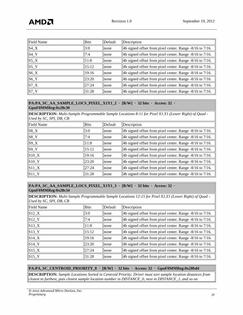
Revision 1.0 September 19, 2012
© 2012 Advanced Micro Devices, Inc. Proprietary 51
Field Name Bits Default Description
S4_X 3:0 none 4b signed offset from pixel center. Range -8/16 to 7/16.
S4_Y 7:4 none 4b signed offset from pixel center. Range -8/16 to 7/16.
S5_X 11:8 none 4b signed offset from pixel center. Range -8/16 to 7/16.
S5_Y 15:12 none 4b signed offset from pixel center. Range -8/16 to 7/16.
S6_X 19:16 none 4b signed offset from pixel center. Range -8/16 to 7/16.
S6_Y 23:20 none 4b signed offset from pixel center. Range -8/16 to 7/16.
S7_X 27:24 none 4b signed offset from pixel center. Range -8/16 to 7/16.
S7_Y 31:28 none 4b signed offset from pixel center. Range -8/16 to 7/16.
PA:PA_SC_AA_SAMPLE_LOCS_PIXEL_X1Y1_2 · [R/W] · 32 bits · Access: 32 ·
GpuF0MMReg:0x28c30
DESCRIPTION: Multi-Sample Programmable Sample Locations 8-11 for Pixel X1,Y1 (Lower Right) of Quad -
Used by SC, SPI, DB, CB
Field Name Bits Default Description
S8_X 3:0 none 4b signed offset from pixel center. Range -8/16 to 7/16.
S8_Y 7:4 none 4b signed offset from pixel center. Range -8/16 to 7/16.
S9_X 11:8 none 4b signed offset from pixel center. Range -8/16 to 7/16.
S9_Y 15:12 none 4b signed offset from pixel center. Range -8/16 to 7/16.
S10_X 19:16 none 4b signed offset from pixel center. Range -8/16 to 7/16.
S10_Y 23:20 none 4b signed offset from pixel center. Range -8/16 to 7/16.
S11_X 27:24 none 4b signed offset from pixel center. Range -8/16 to 7/16.
S11_Y 31:28 none 4b signed offset from pixel center. Range -8/16 to 7/16.
PA:PA_SC_AA_SAMPLE_LOCS_PIXEL_X1Y1_3 · [R/W] · 32 bits · Access: 32 ·
GpuF0MMReg:0x28c34
DESCRIPTION: Multi-Sample Programmable Sample Locations 12-15 for Pixel X1,Y1 (Lower Right) of Quad -
Used by SC, SPI, DB, CB
Field Name Bits Default Description
S12_X 3:0 none 4b signed offset from pixel center. Range -8/16 to 7/16.
S12_Y 7:4 none 4b signed offset from pixel center. Range -8/16 to 7/16.
S13_X 11:8 none 4b signed offset from pixel center. Range -8/16 to 7/16.
S13_Y 15:12 none 4b signed offset from pixel center. Range -8/16 to 7/16.
S14_X 19:16 none 4b signed offset from pixel center. Range -8/16 to 7/16.
S14_Y 23:20 none 4b signed offset from pixel center. Range -8/16 to 7/16.
S15_X 27:24 none 4b signed offset from pixel center. Range -8/16 to 7/16.
S15_Y 31:28 none 4b signed offset from pixel center. Range -8/16 to 7/16.
PA:PA_SC_CENTROID_PRIORITY_0 · [R/W] · 32 bits · Access: 32 · GpuF0MMReg:0x28bd4
DESCRIPTION: Sample Locations Sorted in Centroid Priority; Driver must sort sample location distances from
closest to furthest, puts closest sample location number in DISTANCE_0, next in DISTANCE_1, and so on

Revision 1.0 September 19, 2012
© 2012 Advanced Micro Devices, Inc. Proprietary 52
Field Name Bits Default Description
DISTANCE_0 3:0 none 1st closest sample location to center
DISTANCE_1 7:4 none 2nd closest sample location to center
DISTANCE_2 11:8 none 3rd closest sample location to center
DISTANCE_3 15:12 none 3rd closest sample location to center
DISTANCE_4 19:16 none 4th closest sample location to center
DISTANCE_5 23:20 none 5th closest sample location to center
DISTANCE_6 27:24 none 6th closest sample location to center
DISTANCE_7 31:28 none 7th closest sample location to center
PA:PA_SC_CENTROID_PRIORITY_1 · [R/W] · 32 bits · Access: 32 · GpuF0MMReg:0x28bd8
DESCRIPTION: Sample Locations Sorted in Centroid Priority; Driver must sort sample location distances from
closest to furthest, puts closest sample location number in DISTANCE_0, next in DISTANCE_1, and so on
Field Name Bits Default Description
DISTANCE_8 3:0 none
DISTANCE_9 7:4 none
DISTANCE_10 11:8 none
DISTANCE_11 15:12 none
DISTANCE_12 19:16 none
DISTANCE_13 23:20 none
DISTANCE_14 27:24 none
DISTANCE_15 31:28 none
PA:PA_SC_CLIPRECT_[0-3]_BR · [R/W] · 32 bits · Access: 32 · GpuF0MMReg:0x28214-0x2822c
DESCRIPTION: Clip Rectangle Bottom-Right Specification
Field Name Bits Default Description
BR_X 14:0 none Right x value of clip rectangle. 15 bits unsigned. Valid
range 0-16384. Exclusive for BOTTOM_RIGHT
BR_Y 30:16 none Bottom y value of clip rectangle. 15 bits unsigned. Valid
range 0-16384. Exclusive for BOTTOM_RIGHT
PA:PA_SC_CLIPRECT_[0-3]_TL · [R/W] · 32 bits · Access: 32 · GpuF0MMReg:0x28210-0x28228
DESCRIPTION: Clip Rectangle Top-Left Specification
Field Name Bits Default Description
TL_X 14:0 none Left x value of clip rectangle. 15 bits unsigned. Valid
range 0-16383. Inclusive for UPPER_LEFT
TL_Y 30:16 none Top y value of clip rectangle. 15 bits unsigned. Valid
range 0-16383. Inclusive for UPPER_LEFT
PA:PA_SC_CLIPRECT_RULE · [R/W] · 32 bits · Access: 32 · GpuF0MMReg:0x2820c
DESCRIPTION: OpenGL Clip boolean function

Revision 1.0 September 19, 2012
© 2012 Advanced Micro Devices, Inc. Proprietary 53
Field Name Bits Default Description
CLIP_RULE 15:0 none OpenGL Clip boolean function. The `inside` flags for
each of the four clip rectangles form a 4-bit binary
number. The corresponding bit in this 16-bit number
specifies whether the pixel is visible.
PA:PA_SC_EDGERULE · [R/W] · 32 bits · Access: 32 · GpuF0MMReg:0x28230
DESCRIPTION: Edge Rule Specification
Field Name Bits Default Description
ER_TRI 3:0 none Edge rule for triangles; L:R:T:B -> 1 = in, 0 = out
ER_POINT 7:4 none Edge rule for points; L:R:T:B -> 1 = in, 0 = out
ER_RECT 11:8 none Edge rule for rects; L:R:T:B -> 1 = in, 0 = out
ER_LINE_LR 17:12 none Edge rule for left-right lines;
TB_L:TB_R:BT_L:BT_R:HT:HB -> 1 = in, 0 = out. If
PA_SC_LINE_CNTL.DX10_DIAMOND_TEST_ENA
is set, this field needs to be set to a 0x1A
ER_LINE_RL 23:18 none Edge rule for right-left lines;
TB_L:TB_R:BT_L:BT_R:HT:HB -> 1 = in, 0 = out. If
PA_SC_LINE_CNTL.DX10_DIAMOND_TEST_ENA
is set, this field needs to be set to a 0x26
ER_LINE_TB 27:24 none Edge rule for top-bottom lines;
LR_L:LR_R:RL_L:RL_R -> 1 = in, 0 = out. If
PA_SC_LINE_CNTL.DX10_DIAMOND_TEST_ENA
is set, this field needs to be set to a 0xA
ER_LINE_BT 31:28 none Edge rule for bottom-top lines;
LR_L:LR_R:RL_L:RL_R -> 1 = in, 0 = out. If
PA_SC_LINE_CNTL.DX10_DIAMOND_TEST_ENA
is set, this field needs to be set to a 0xA
PA:PA_SC_ENHANCE · [R/W] · 32 bits · Access: 32 · GpuF0MMReg:0x8bf0
DESCRIPTION: Used for Late Additions of Control Bits
Field Name Bits Default Description
ENABLE_PA_SC_OUT_OF_ORDER 0 0x0 Allow PA_SC out of order to be enabled,
including EndOfPacket on both PA
inputs.
DISABLE_SC_DB_TILE_FIX 1 0x0 Disable fix for SC_DB_tile fix
DISABLE_AA_MASK_FULL_FIX 2 0x0 Disable fix for considering MSAA level
when looking at aa_mask full for
SC_DB_tile_covered.
ENABLE_1XMSAA_SAMPLE_LOCATIONS 3 0x0 Enable 1XMSAA to use the sample loc
regs, and not assume samples are at pixel
center.
ENABLE_1XMSAA_SAMPLE_LOC_CENTROID 4 0x0 Distinguish between pixel center and
centroid for 1xMSAA.
DISABLE_SCISSOR_FIX 5 0x0 Disable scissor fix for bottom-right
scissors at 0 or 1, and revert to 9xx
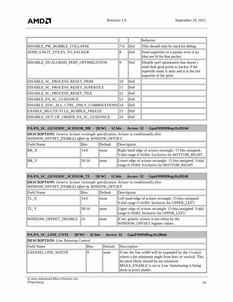
Revision 1.0 September 19, 2012
© 2012 Advanced Micro Devices, Inc. Proprietary 54
behavior.
DISABLE_PW_BUBBLE_COLLAPSE 7:6 0x0 This should only be used for debug.
SEND_UNLIT_STILES_TO_PACKER 8 0x0 Send supertiles to a packer even if no
tiles are lit for that packer.
DISABLE_DUALGRAD_PERF_OPTIMIZATION 9 0x0 Disable perf optimiation that doesn`t
send dual grad prims to packer if the
supertile mask is unlit and it is the last
supertile of the prim.
DISABLE_SC_PROCESS_RESET_PRIM 10 0x0
DISABLE_SC_PROCESS_RESET_SUPERTILE 11 0x0
DISABLE_SC_PROCESS_RESET_TILE 12 0x0
DISABLE_PA_SC_GUIDANCE 13 0x0
DISABLE_EOV_ALL_CTRL_ONLY_COMBINATIONS 14 0x0
ENABLE_MULTICYCLE_BUBBLE_FREEZE 15 0x0
DISABLE_OUT_OF_ORDER_PA_SC_GUIDANCE 16 0x0
PA:PA_SC_GENERIC_SCISSOR_BR · [R/W] · 32 bits · Access: 32 · GpuF0MMReg:0x28244
DESCRIPTION: Generic Scissor rectangle specification. Scissor is conditionally (See
WINDOW_OFFSET_ENABLE) offset by WINDOW_OFFSET.
Field Name Bits Default Description
BR_X 14:0 none Right hand edge of scissor rectangle. 15 bits unsigned.
Valid range 0-16384. Exclusive for BOTTOM_RIGHT.
BR_Y 30:16 none Lower edge of scissor rectangle. 15 bits unsigned. Valid
range 0-16384. Exclusive for BOTTOM_RIGHT.
PA:PA_SC_GENERIC_SCISSOR_TL · [R/W] · 32 bits · Access: 32 · GpuF0MMReg:0x28240
DESCRIPTION: Generic Scissor rectangle specification. Scissor is conditionally (See
WINDOW_OFFSET_ENABLE) offset by WINDOW_OFFSET.
Field Name Bits Default Description
TL_X 14:0 none Left hand edge of scissor rectangle. 15-bits unsigned.
Valid range 0-16383. Inclusive for UPPER_LEFT.
TL_Y 30:16 none Upper edge of scissor rectangle. 15-bits unsigned. Valid
range 0-16383. Inclusive for UPPER_LEFT.
WINDOW_OFFSET_DISABLE 31 none If set, generic scissor is not offset by the
WINDOW_OFFSET register values.
PA:PA_SC_LINE_CNTL · [R/W] · 32 bits · Access: 32 · GpuF0MMReg:0x28bdc
DESCRIPTION: Line Drawing Control
Field Name Bits Default Description
EXPAND_LINE_WIDTH 9 none If set, the line width will be expanded by the 1/cos(a)
where a the minimum angle from horz or vertical. This
bit most likely should be set whenever
MSAA_ENABLE is set or Line Antialiasing is being
done in pixel shader.
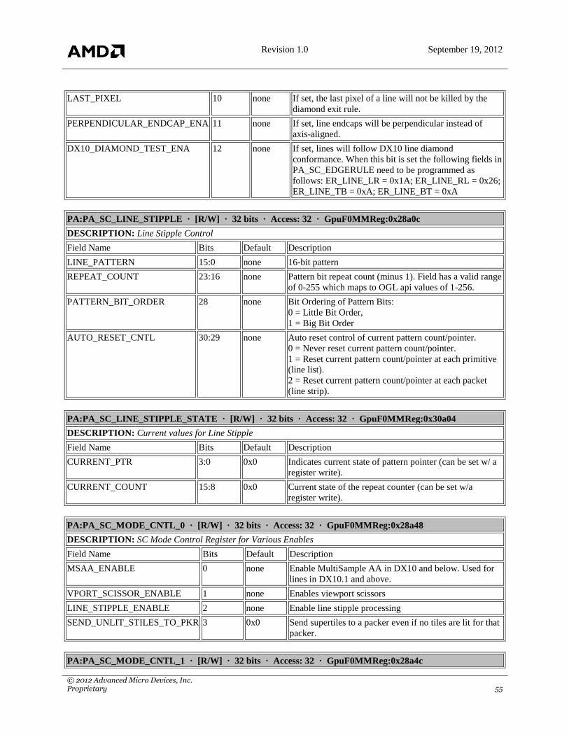
Revision 1.0 September 19, 2012
© 2012 Advanced Micro Devices, Inc. Proprietary 55
LAST_PIXEL 10 none If set, the last pixel of a line will not be killed by the
diamond exit rule.
PERPENDICULAR_ENDCAP_ENA 11 none If set, line endcaps will be perpendicular instead of
axis-aligned.
DX10_DIAMOND_TEST_ENA 12 none If set, lines will follow DX10 line diamond
conformance. When this bit is set the following fields in
PA_SC_EDGERULE need to be programmed as
follows: ER_LINE_LR = 0x1A; ER_LINE_RL = 0x26;
ER_LINE_TB = 0xA; ER_LINE_BT = 0xA
PA:PA_SC_LINE_STIPPLE · [R/W] · 32 bits · Access: 32 · GpuF0MMReg:0x28a0c
DESCRIPTION: Line Stipple Control
Field Name Bits Default Description
LINE_PATTERN 15:0 none 16-bit pattern
REPEAT_COUNT 23:16 none Pattern bit repeat count (minus 1). Field has a valid range
of 0-255 which maps to OGL api values of 1-256.
PATTERN_BIT_ORDER 28 none Bit Ordering of Pattern Bits:
0 = Little Bit Order,
1 = Big Bit Order
AUTO_RESET_CNTL 30:29 none Auto reset control of current pattern count/pointer.
0 = Never reset current pattern count/pointer.
1 = Reset current pattern count/pointer at each primitive
(line list).
2 = Reset current pattern count/pointer at each packet
(line strip).
PA:PA_SC_LINE_STIPPLE_STATE · [R/W] · 32 bits · Access: 32 · GpuF0MMReg:0x30a04
DESCRIPTION: Current values for Line Stipple
Field Name Bits Default Description
CURRENT_PTR 3:0 0x0 Indicates current state of pattern pointer (can be set w/ a
register write).
CURRENT_COUNT 15:8 0x0 Current state of the repeat counter (can be set w/a
register write).
PA:PA_SC_MODE_CNTL_0 · [R/W] · 32 bits · Access: 32 · GpuF0MMReg:0x28a48
DESCRIPTION: SC Mode Control Register for Various Enables
Field Name Bits Default Description
MSAA_ENABLE 0 none Enable MultiSample AA in DX10 and below. Used for
lines in DX10.1 and above.
VPORT_SCISSOR_ENABLE 1 none Enables viewport scissors
LINE_STIPPLE_ENABLE 2 none Enable line stipple processing
SEND_UNLIT_STILES_TO_PKR 3 0x0 Send supertiles to a packer even if no tiles are lit for that
packer.
PA:PA_SC_MODE_CNTL_1 · [R/W] · 32 bits · Access: 32 · GpuF0MMReg:0x28a4c

Revision 1.0 September 19, 2012
© 2012 Advanced Micro Devices, Inc. Proprietary 56
DESCRIPTION: SC Mode Control Register for Various Enables
Field Name Bits Defa
ult Description
WALK_SIZE 0 0x0 Defines the size of the SC walk stamp. 0 : walk by
supertiles (32 bits); 1 : walk by tiles (8 bits)
WALK_ALIGNMENT 1 0x0 Defines the alignment value of the SC walker. 0 : align by
supertiles (32 bits); 1 : align by tiles (8 bits)
WALK_ALIGN8_PRIM_FITS_ST 2 0x0 When alignment value is set to supertiles (32 bits), enables
the walker to align by tiles (8 bits) if primitive fits within
one supertile
WALK_FENCE_ENABLE 3 0x0 Enable primitive walk order that walks programmable
width size rectangular areas; vertical fences
WALK_FENCE_SIZE 6:4 0x0 Size of fence in pixels, 0: 64; 1: 128; 2: 256; 3: 512
SUPERTILE_WALK_ORDER_ENABLE 7 0x0 Enables fixed pattern for walking tiles in a supertile
TILE_WALK_ORDER_ENABLE 8 0x0 Enables fixed pattern for walking quads in a tile. Must be
disabled for overlapping blit rendering
TILE_COVER_DISABLE 9 0x0 Disables tile covered (Hi-Z optimization) that is sent to the
DBs
TILE_COVER_NO_SCISSOR 10 0x0 Disables the use of scissors when determining tile covered
ZMM_LINE_EXTENT 11 0x0 When rendering lines, push ZMin/ZMax to the extent to
avoid Z values outside the ZMin/ZMax range
ZMM_LINE_OFFSET 12 0x0 When rendering lines, offset ZMin/ZMax by next largest
power of 2 above dZ/dx or dZ/dy to avoid Z values outside
the ZMin/ZMax range
ZMM_RECT_EXTENT 13 0x0 When rendering rects, push ZMin/ZMax to the extent to
avoid Z values outside the ZMin/ZMax range
KILL_PIX_POST_HI_Z 14 0x0 If set, all pixels are killed in the SC after the Hi-Z test.
Typically set for VizQuery geometry
KILL_PIX_POST_DETAIL_MASK 15 0x0 If set, all pixels are killed in the SC after the detail mask.
Can be used for performance info
PS_ITER_SAMPLE 16 0x0 Enables per-sample (i.e. unique shader-computed value
per sample) pixel shader execution
MULTI_SHADER_ENGINE_PRIM_DISC
ARD_ENABLE
17 0x0 Enables primitives to be discarded based on multi-shader
engine settings
FORCE_EOV_CNTDWN_ENABLE 25 0x1 Enables forcing out pixel vectors prematurely based on the
cycle count programmed in
PA_SC_FORCE_EOV_MAX_CNTS::FORCE_EOV_MA
X_CLK_CNT[13:0]
FORCE_EOV_REZ_ENABLE 26 0x1 Enables forcing out pixel vectors prematurely based on the
ReZ hang condition(ie. cache locked) detected in the DB;
after receiving DB signal wait cycle count programmed in
PA_SC_FORCE_EOV_MAX_CNTS::FORCE_EOV_MA
X_REZ_CNT[13:0]
OUT_OF_ORDER_PRIMITIVE_ENABLE 27 0x0 For configurations with more than one PA, enables the
ability of the SC to operate on primitives out of order in
case the primitive stream is out of balance flooding one SC
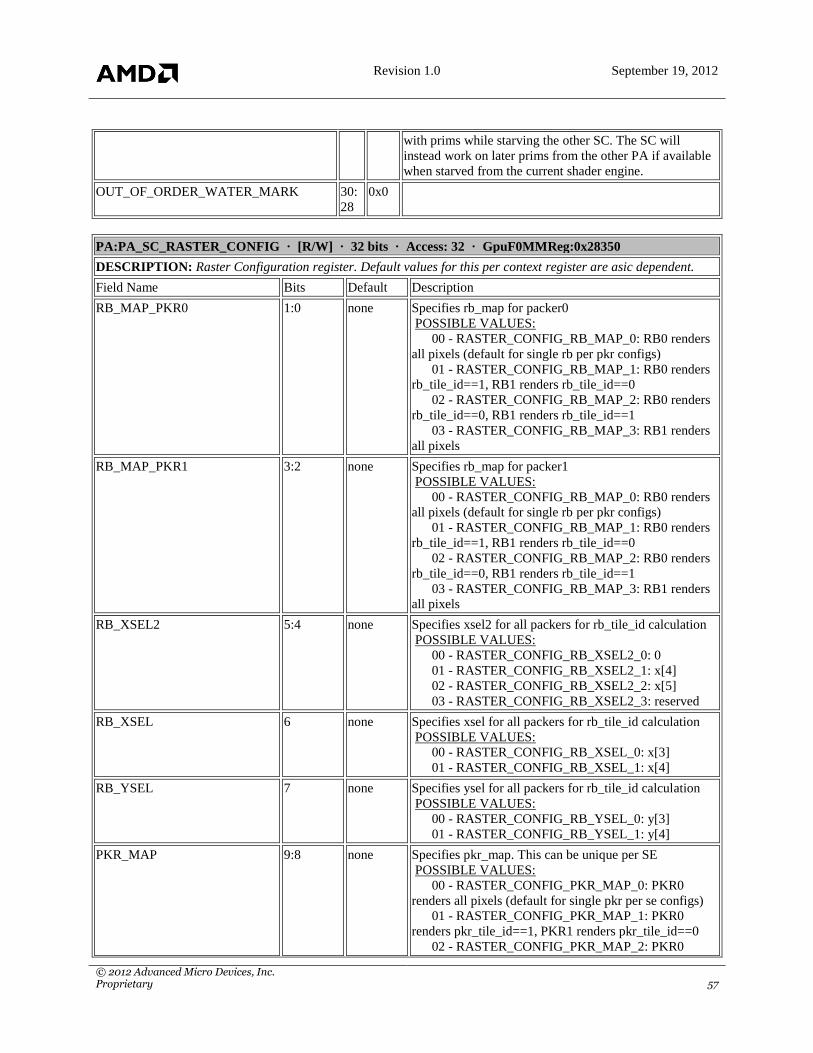
Revision 1.0 September 19, 2012
© 2012 Advanced Micro Devices, Inc. Proprietary 57
with prims while starving the other SC. The SC will
instead work on later prims from the other PA if available
when starved from the current shader engine.
OUT_OF_ORDER_WATER_MARK 30:
28
0x0
PA:PA_SC_RASTER_CONFIG · [R/W] · 32 bits · Access: 32 · GpuF0MMReg:0x28350
DESCRIPTION: Raster Configuration register. Default values for this per context register are asic dependent.
Field Name Bits Default Description
RB_MAP_PKR0 1:0 none Specifies rb_map for packer0
POSSIBLE VALUES:
00 - RASTER_CONFIG_RB_MAP_0: RB0 renders
all pixels (default for single rb per pkr configs)
01 - RASTER_CONFIG_RB_MAP_1: RB0 renders
rb_tile_id==1, RB1 renders rb_tile_id==0
02 - RASTER_CONFIG_RB_MAP_2: RB0 renders
rb_tile_id==0, RB1 renders rb_tile_id==1
03 - RASTER_CONFIG_RB_MAP_3: RB1 renders
all pixels
RB_MAP_PKR1 3:2 none Specifies rb_map for packer1
POSSIBLE VALUES:
00 - RASTER_CONFIG_RB_MAP_0: RB0 renders
all pixels (default for single rb per pkr configs)
01 - RASTER_CONFIG_RB_MAP_1: RB0 renders
rb_tile_id==1, RB1 renders rb_tile_id==0
02 - RASTER_CONFIG_RB_MAP_2: RB0 renders
rb_tile_id==0, RB1 renders rb_tile_id==1
03 - RASTER_CONFIG_RB_MAP_3: RB1 renders
all pixels
RB_XSEL2 5:4 none Specifies xsel2 for all packers for rb_tile_id calculation
POSSIBLE VALUES:
00 - RASTER_CONFIG_RB_XSEL2_0: 0
01 - RASTER_CONFIG_RB_XSEL2_1: x[4]
02 - RASTER_CONFIG_RB_XSEL2_2: x[5]
03 - RASTER_CONFIG_RB_XSEL2_3: reserved
RB_XSEL 6 none Specifies xsel for all packers for rb_tile_id calculation
POSSIBLE VALUES:
00 - RASTER_CONFIG_RB_XSEL_0: x[3]
01 - RASTER_CONFIG_RB_XSEL_1: x[4]
RB_YSEL 7 none Specifies ysel for all packers for rb_tile_id calculation
POSSIBLE VALUES:
00 - RASTER_CONFIG_RB_YSEL_0: y[3]
01 - RASTER_CONFIG_RB_YSEL_1: y[4]
PKR_MAP 9:8 none Specifies pkr_map. This can be unique per SE
POSSIBLE VALUES:
00 - RASTER_CONFIG_PKR_MAP_0: PKR0
renders all pixels (default for single pkr per se configs)
01 - RASTER_CONFIG_PKR_MAP_1: PKR0
renders pkr_tile_id==1, PKR1 renders pkr_tile_id==0
02 - RASTER_CONFIG_PKR_MAP_2: PKR0

Revision 1.0 September 19, 2012
© 2012 Advanced Micro Devices, Inc. Proprietary 58
renders pkr_tile_id==0, PKR1 renders pkr_tile_id==1
03 - RASTER_CONFIG_PKR_MAP_3: PKR1
renders all pixels
PKR_XSEL 11:10 none Specifies xsel for all pkr to be used in pkr_tile_id
calculation
POSSIBLE VALUES:
00 - RASTER_CONFIG_PKR_XSEL_0: x[3]
01 - RASTER_CONFIG_PKR_XSEL_1: x[4]
02 - RASTER_CONFIG_PKR_XSEL_2: x[5]
03 - RASTER_CONFIG_PKR_XSEL_3: x[6]
PKR_YSEL 13:12 none Specifies ysel for all pkr to be used in pkr_tile_id
calculation
POSSIBLE VALUES:
00 - RASTER_CONFIG_PKR_YSEL_0: y[3]
01 - RASTER_CONFIG_PKR_YSEL_1: y[4]
02 - RASTER_CONFIG_PKR_YSEL_2: y[5]
03 - RASTER_CONFIG_PKR_YSEL_3: y[6]
SC_MAP 17:16 none Reserved for 2 SC per SE Configs. Set to 0 for Default
POSSIBLE VALUES:
00 - RASTER_CONFIG_SC_MAP_0: SC0 renders
all pixels (default for single SC per SE configs)
01 - RASTER_CONFIG_SC_MAP_1: SC0 renders
sc_tile_id==1, SC1 renders sc_tile_id==0
02 - RASTER_CONFIG_SC_MAP_2: SC0 renders
sc_tile_id==0, SC1 renders sc_tile_id==1
03 - RASTER_CONFIG_SC_MAP_3: SC1 renders
all pixels
SC_XSEL 19:18 none Reserved for 2 SC Per SE Configs. Set to 0 for Default
POSSIBLE VALUES:
00 -
RASTER_CONFIG_SC_XSEL_8_WIDE_TILE: 8 wide
tile
01 -
RASTER_CONFIG_SC_XSEL_16_WIDE_TILE: 16
wide tile
02 -
RASTER_CONFIG_SC_XSEL_32_WIDE_TILE: 32
wide tile
03 -
RASTER_CONFIG_SC_XSEL_64_WIDE_TILE: 64
wide tile
SC_YSEL 21:20 none Reserved for 2 SC Per SE Configs. Set to 0 for Default
POSSIBLE VALUES:
00 -
RASTER_CONFIG_SC_YSEL_8_WIDE_TILE: 8 wide
tile
01 -
RASTER_CONFIG_SC_YSEL_16_WIDE_TILE: 16
wide tile
02 -
RASTER_CONFIG_SC_YSEL_32_WIDE_TILE: 32

Revision 1.0 September 19, 2012
© 2012 Advanced Micro Devices, Inc. Proprietary 59
wide tile
03 -
RASTER_CONFIG_SC_YSEL_64_WIDE_TILE: 64
wide tile
SE_MAP 25:24 none Specifies se_map use for mapping se_tile_id to an SE
instance
POSSIBLE VALUES:
00 - RASTER_CONFIG_SE_MAP_0: SE0 renders
all pixels (default for single SE configs)
01 - RASTER_CONFIG_SE_MAP_1: SE0 renders
se_tile_id==1, SE1 renders se_tile_id==0
02 - RASTER_CONFIG_SE_MAP_2: SE0 renders
se_tile_id==0, SE1 renders se_tile_id==1
03 - RASTER_CONFIG_SE_MAP_3: SE1 renders
all pixels
SE_XSEL 27:26 none Specifies xsel used in se_tile_id calculation
POSSIBLE VALUES:
00 -
RASTER_CONFIG_SE_XSEL_8_WIDE_TILE: 8 wide
tile
01 -
RASTER_CONFIG_SE_XSEL_16_WIDE_TILE: 16
wide tile
02 -
RASTER_CONFIG_SE_XSEL_32_WIDE_TILE: 32
wide tile
03 -
RASTER_CONFIG_SE_XSEL_64_WIDE_TILE: 64
wide tile
SE_YSEL 29:28 none Specifies ysel used in se_tile_id calculation
POSSIBLE VALUES:
00 -
RASTER_CONFIG_SE_YSEL_8_WIDE_TILE: 8 wide
tile
01 -
RASTER_CONFIG_SE_YSEL_16_WIDE_TILE: 16
wide tile
02 -
RASTER_CONFIG_SE_YSEL_32_WIDE_TILE: 32
wide tile
03 -
RASTER_CONFIG_SE_YSEL_64_WIDE_TILE: 64
wide tile
PA:PA_SC_RASTER_CONFIG_1 · [R/W] · 32 bits · Access: 32 · GpuF0MMReg:0x28354
DESCRIPTION: Raster Configuration 1 register. Default values for this per context register are asic dependent.
Field Name Bits Default Description
SE_PAIR_MAP 1:0 none Specifies se_pair_map use for mapping se_pair_tile_id.
Set to non 0 default only for 4 SE configs
POSSIBLE VALUES:
00 - RASTER_CONFIG_SE_PAIR_MAP_0: First

Revision 1.0 September 19, 2012
© 2012 Advanced Micro Devices, Inc. Proprietary 60
SE pair ie SE0/1 renders all pixels.
01 - RASTER_CONFIG_SE_PAIR_MAP_1: SE0/1
renders se_pair_tile_id==1, SE2/3 renders
se_pair_tile_id==0
02 - RASTER_CONFIG_SE_PAIR_MAP_2: SE0/1
renders se_pair_tile_id==0, SE2/3 renders
se_pair_tile_id==1
03 - RASTER_CONFIG_SE_PAIR_MAP_3: Second
SE pair ie SE2/3 renders all pixels
SE_PAIR_XSEL 3:2 none Specifies xsel used in se_pair_tile_id calculation
POSSIBLE VALUES:
00 -
RASTER_CONFIG_SE_PAIR_XSEL_8_WIDE_TILE:
8 wide tile
01 -
RASTER_CONFIG_SE_PAIR_XSEL_16_WIDE_TILE:
16 wide tile
02 -
RASTER_CONFIG_SE_PAIR_XSEL_32_WIDE_TILE:
32 wide tile
03 -
RASTER_CONFIG_SE_PAIR_XSEL_64_WIDE_TILE:
64 wide tile
SE_PAIR_YSEL 5:4 none Specifies ysel used in se_pair_tile_id calculation
POSSIBLE VALUES:
00 -
RASTER_CONFIG_SE_PAIR_YSEL_8_WIDE_TILE:
8 wide tile
01 -
RASTER_CONFIG_SE_PAIR_YSEL_16_WIDE_TILE:
16 wide tile
02 -
RASTER_CONFIG_SE_PAIR_YSEL_32_WIDE_TILE:
32 wide tile
03 -
RASTER_CONFIG_SE_PAIR_YSEL_64_WIDE_TILE:
64 wide tile
PA:PA_SC_SCREEN_SCISSOR_BR · [R/W] · 32 bits · Access: 32 · GpuF0MMReg:0x28034
DESCRIPTION: Screen Scissor rectangle specification. This scissor is NOT affected by WINDOW_OFFSET.
Negative numbers clamped to 0, so reads will mismatch on negative values.
Field Name Bits Default Description
BR_X 15:0 none Right hand edge of scissor rectangle. 16 bits signed.
Valid range -32K to 16384. Exclusive for
BOTTOM_RIGHT.
BR_Y 31:16 none Lower edge of scissor rectangle. 16 bits signed. Valid
range -32K to 16384. Exclusive for BOTTOM_RIGHT.
PA:PA_SC_SCREEN_SCISSOR_TL · [R/W] · 32 bits · Access: 32 · GpuF0MMReg:0x28030
DESCRIPTION: Screen Scissor rectangle specification. This scissor is NOT affected by WINDOW_OFFSET.
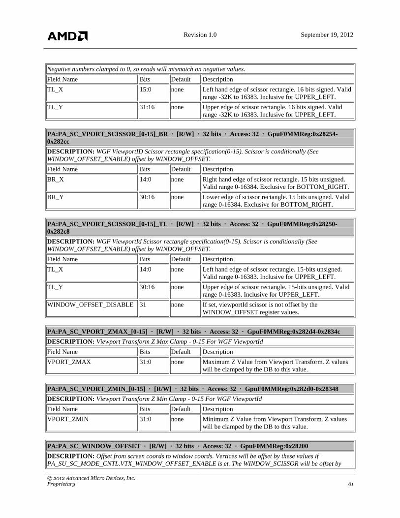
Revision 1.0 September 19, 2012
© 2012 Advanced Micro Devices, Inc. Proprietary 61
Negative numbers clamped to 0, so reads will mismatch on negative values.
Field Name Bits Default Description
TL_X 15:0 none Left hand edge of scissor rectangle. 16 bits signed. Valid
range -32K to 16383. Inclusive for UPPER_LEFT.
TL_Y 31:16 none Upper edge of scissor rectangle. 16 bits signed. Valid
range -32K to 16383. Inclusive for UPPER_LEFT.
PA:PA_SC_VPORT_SCISSOR_[0-15]_BR · [R/W] · 32 bits · Access: 32 · GpuF0MMReg:0x28254-
0x282cc
DESCRIPTION: WGF ViewportID Scissor rectangle specification(0-15). Scissor is conditionally (See
WINDOW_OFFSET_ENABLE) offset by WINDOW_OFFSET.
Field Name Bits Default Description
BR_X 14:0 none Right hand edge of scissor rectangle. 15 bits unsigned.
Valid range 0-16384. Exclusive for BOTTOM_RIGHT.
BR_Y 30:16 none Lower edge of scissor rectangle. 15 bits unsigned. Valid
range 0-16384. Exclusive for BOTTOM_RIGHT.
PA:PA_SC_VPORT_SCISSOR_[0-15]_TL · [R/W] · 32 bits · Access: 32 · GpuF0MMReg:0x28250-
0x282c8
DESCRIPTION: WGF ViewportId Scissor rectangle specification(0-15). Scissor is conditionally (See
WINDOW_OFFSET_ENABLE) offset by WINDOW_OFFSET.
Field Name Bits Default Description
TL_X 14:0 none Left hand edge of scissor rectangle. 15-bits unsigned.
Valid range 0-16383. Inclusive for UPPER_LEFT.
TL_Y 30:16 none Upper edge of scissor rectangle. 15-bits unsigned. Valid
range 0-16383. Inclusive for UPPER_LEFT.
WINDOW_OFFSET_DISABLE 31 none If set, viewportId scissor is not offset by the
WINDOW_OFFSET register values.
PA:PA_SC_VPORT_ZMAX_[0-15] · [R/W] · 32 bits · Access: 32 · GpuF0MMReg:0x282d4-0x2834c
DESCRIPTION: Viewport Transform Z Max Clamp - 0-15 For WGF ViewportId
Field Name Bits Default Description
VPORT_ZMAX 31:0 none Maximum Z Value from Viewport Transform. Z values
will be clamped by the DB to this value.
PA:PA_SC_VPORT_ZMIN_[0-15] · [R/W] · 32 bits · Access: 32 · GpuF0MMReg:0x282d0-0x28348
DESCRIPTION: Viewport Transform Z Min Clamp - 0-15 For WGF ViewportId
Field Name Bits Default Description
VPORT_ZMIN 31:0 none Minimum Z Value from Viewport Transform. Z values
will be clamped by the DB to this value.
PA:PA_SC_WINDOW_OFFSET · [R/W] · 32 bits · Access: 32 · GpuF0MMReg:0x28200
DESCRIPTION: Offset from screen coords to window coords. Vertices will be offset by these values if
PA_SU_SC_MODE_CNTL.VTX_WINDOW_OFFSET_ENABLE is et. The WINDOW_SCISSOR will be offset by

Revision 1.0 September 19, 2012
© 2012 Advanced Micro Devices, Inc. Proprietary 62
these values if the WINDOW_SCISSOR_TL.WINDOW_OFFSET_DISABLE is clear. If this value allows the window
to extend beyond the Front Buffer (Surface) dimensions, it is expected that the SCREEN_SCISSOR is used to limit to
FB surface.
Field Name Bits Default Description
WINDOW_X_OFFSET 15:0 none Offset in x-direction from screen to window coords. 16-
bit 2`s comp signed value. Valid Range +/- 32K.
WINDOW_Y_OFFSET 31:16 none Offset in y-direction from screen to window coords. 16-
bit 2`s comp signed value. Valid Range +/- 32K.
PA:PA_SC_WINDOW_SCISSOR_BR · [R/W] · 32 bits · Access: 32 · GpuF0MMReg:0x28208
DESCRIPTION: Window Scissor rectangle specification. Scissor is conditionally (See
WINDOW_OFFSET_ENABLE) offset by WINDOW_OFFSET.
Field Name Bits Default Description
BR_X 14:0 none Right hand edge of scissor rectangle. 15 bits unsigned.
Valid range 0-16384. Exclusive for BOTTOM_RIGHT.
BR_Y 30:16 none Lower edge of scissor rectangle. 15 bits unsigned. Valid
range 0-16384. Exclusive for BOTTOM_RIGHT.
PA:PA_SC_WINDOW_SCISSOR_TL · [R/W] · 32 bits · Access: 32 · GpuF0MMReg:0x28204
DESCRIPTION: Window Scissor rectangle specification. Scissor is conditionally (See
WINDOW_OFFSET_ENABLE) offset by WINDOW_OFFSET.
Field Name Bits Default Description
TL_X 14:0 none Left hand edge of scissor rectangle. 15-bits unsigned.
Valid range 0-16383. Inclusive for UPPER_LEFT.
TL_Y 30:16 none Upper edge of scissor rectangle. 15-bits unsigned. Valid
range 0-16383. Inclusive for UPPER_LEFT.
WINDOW_OFFSET_DISABLE 31 none If set, window scissor is not offset by the
WINDOW_OFFSET register values.
PA:PA_SU_CNTL_STATUS · [R] · 32 bits · Access: 32 · GpuF0MMReg:0x8a50
DESCRIPTION: Status Bits
Field Name Bits Default Description
SU_BUSY 31 none Busy Status Bit
PA:PA_SU_HARDWARE_SCREEN_OFFSET · [R/W] · 32 bits · Access: 32 · GpuF0MMReg:0x28234
DESCRIPTION: Hardware Screen Offset to Center Guardband
Field Name Bits Default Description
HW_SCREEN_OFFSET_X 8:0 none Hardware screen offset in X from 0 to 8176 in units of 16
pixels.
HW_SCREEN_OFFSET_Y 24:16 none Hardware screen offset in Y from 0 to 8176 in units of 16
pixels.
PA:PA_SU_LINE_CNTL · [R/W] · 32 bits · Access: 32 · GpuF0MMReg:0x28a08

Revision 1.0 September 19, 2012
© 2012 Advanced Micro Devices, Inc. Proprietary 63
DESCRIPTION: Line control
Field Name Bits Default Description
WIDTH 15:0 none 1/2 width of line, in subpixels; (16.0) fixed format.
PA:PA_SU_LINE_STIPPLE_CNTL · [R/W] · 32 bits · Access: 32 · GpuF0MMReg:0x28824
DESCRIPTION: Set-Up Engine Line Stipple Control
Field Name Bits Default Description
LINE_STIPPLE_RESET 1:0 none line stipple reset mode: 0-no reset, 1-end of prim, 2-end
of packet, 3-end of polymode line.
EXPAND_FULL_LENGTH 2 none for antialiased line stipple, calculate stipple distance
using true distance (not major).
FRACTIONAL_ACCUM 3 none for antialiased line stipple, calculate stipple using
travelled distance including fractional bits.
DIAMOND_ADJUST 4 none for aliased line stipple, adjust stipple pattern to account
for start vertex diamond exit .
PA:PA_SU_LINE_STIPPLE_SCALE · [R/W] · 32 bits · Access: 32 · GpuF0MMReg:0x28828
DESCRIPTION: Set-Up Engine Line Stipple Scale Factor
Field Name Bits Default Description
LINE_STIPPLE_SCALE 31:0 none floating point scale factor used to derive stipple start and
end point.
PA:PA_SU_LINE_STIPPLE_VALUE · [R/W] · 32 bits · Access: 32 · GpuF0MMReg:0x30a00
DESCRIPTION: Current value for Set-Up Engine Line Stipple
Field Name Bits Default Description
LINE_STIPPLE_VALUE 23:0 none Current value for line stipple with 8 fractional.
PA:PA_SU_POINT_MINMAX · [R/W] · 32 bits · Access: 32 · GpuF0MMReg:0x28a04
DESCRIPTION: Specifies maximum and minimum point & sprite sizes for per vertex size specification.
Field Name Bits Default Description
MIN_SIZE 15:0 none Minimum point & sprite radius size to allow. fixed point
(12.4), 12 bits integer, 4 bits fractional pixels
MAX_SIZE 31:16 none Maximum point & sprite radius size to allow. fixed point
(12.4), 12 bits integer, 4 bits fractional pixels
PA:PA_SU_POINT_SIZE · [R/W] · 32 bits · Access: 32 · GpuF0MMReg:0x28a00
DESCRIPTION: Dimensions for Points
Field Name Bits Default Description
HEIGHT 15:0 none 1/2 Height (Vertical Radius) of point; fixed (12.4), 12
bits integer, 4 bits fractional pixels.
WIDTH 31:16 none 1/2 Width (Horizontal Radius)of point; fixed (12.4), 12
bits integer, 4 bits fractional pixels.
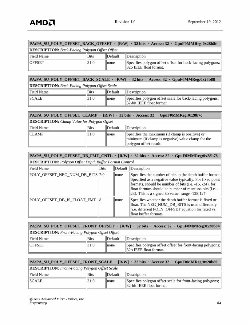
Revision 1.0 September 19, 2012
© 2012 Advanced Micro Devices, Inc. Proprietary 64
PA:PA_SU_POLY_OFFSET_BACK_OFFSET · [R/W] · 32 bits · Access: 32 · GpuF0MMReg:0x28b8c
DESCRIPTION: Back-Facing Polygon Offset Offset
Field Name Bits Default Description
OFFSET 31:0 none Specifies polygon offset offset for back-facing polygons;
32b IEEE float format.
PA:PA_SU_POLY_OFFSET_BACK_SCALE · [R/W] · 32 bits · Access: 32 · GpuF0MMReg:0x28b88
DESCRIPTION: Back-Facing Polygon Offset Scale
Field Name Bits Default Description
SCALE 31:0 none Specifies polygon offset scale for back-facing polygons;
32-bit IEEE float format.
PA:PA_SU_POLY_OFFSET_CLAMP · [R/W] · 32 bits · Access: 32 · GpuF0MMReg:0x28b7c
DESCRIPTION: Clamp Value for Polygon Offset
Field Name Bits Default Description
CLAMP 31:0 none Specifies the maximum (if clamp is positive) or
minimum (if clamp is negative) value clamp for the
polygon offset result.
PA:PA_SU_POLY_OFFSET_DB_FMT_CNTL · [R/W] · 32 bits · Access: 32 · GpuF0MMReg:0x28b78
DESCRIPTION: Polygon Offset Depth Buffer Format Control
Field Name Bits Default Description
POLY_OFFSET_NEG_NUM_DB_BITS 7:0 none Specifies the number of bits in the depth buffer format.
Specified as a negative value typically. For fixed point
formats, should be number of bits (i.e. -16, -24), for
float formats should be number of mantissa bits (i.e. -
23). This is a signed 8b value, range -128,127
POLY_OFFSET_DB_IS_FLOAT_FMT 8 none Specifies whether the depth buffer format is fixed or
float. The NEG_NUM_DB_BITS is used differently
(i.e. different POLY_OFFSET equation for fixed vs.
float buffer formats.
PA:PA_SU_POLY_OFFSET_FRONT_OFFSET · [R/W] · 32 bits · Access: 32 · GpuF0MMReg:0x28b84
DESCRIPTION: Front-Facing Polygon Offset Offset
Field Name Bits Default Description
OFFSET 31:0 none Specifies polygon offset offset for front-facing polygons;
32b IEEE float format.
PA:PA_SU_POLY_OFFSET_FRONT_SCALE · [R/W] · 32 bits · Access: 32 · GpuF0MMReg:0x28b80
DESCRIPTION: Front-Facing Polygon Offset Scale
Field Name Bits Default Description
SCALE 31:0 none Specifies polygon offset scale for front-facing polygons;
32-bit IEEE float format.

Revision 1.0 September 19, 2012
© 2012 Advanced Micro Devices, Inc. Proprietary 65
PA:PA_SU_PRIM_FILTER_CNTL · [R/W] · 32 bits · Access: 32 · GpuF0MMReg:0x2882c
DESCRIPTION: Set-Up Engine Primitive Filter Control
Field Name Bits Default Description
TRIANGLE_FILTER_DISABLE 0 none for triangle primitive type, disable primitive filters.
LINE_FILTER_DISABLE 1 none for line primitive type, disable primitive filters.
POINT_FILTER_DISABLE 2 none for point primitive type, disable primitive filters.
RECTANGLE_FILTER_DISABLE 3 none for rectangle primitive type, disable primitive filters.
TRIANGLE_EXPAND_ENA 4 none for triangle primitive type, expand primitive bounding
box for prim filters.
LINE_EXPAND_ENA 5 none for line primitive type, expand primitive bounding box
for prim filters.
POINT_EXPAND_ENA 6 none for point primitive type, expand primitive bounding box
for prim filters.
RECTANGLE_EXPAND_ENA 7 none for rectangle primitive type, expand primitive bounding
box for prim filters.
PRIM_EXPAND_CONSTANT 15:8 none constant [4.4] to expand each edge of bounding box
before prim filter test.
XMAX_RIGHT_EXCLUSION 30 none
YMAX_BOTTOM_EXCLUSION 31 none
PA:PA_SU_SC_MODE_CNTL · [R/W] · 32 bits · Access: 32 · GpuF0MMReg:0x28814
DESCRIPTION: SU/SC Controls for Facedness Culling, Polymode, Polygon Offset, and various Enables
Field Name Bits Default Description
CULL_FRONT 0 none Enable for front-face culling.
POSSIBLE VALUES:
00 - Do not cull front-facing triangles.
01 - Cull front-facing triangles.
CULL_BACK 1 none Enable for back-face culling.
POSSIBLE VALUES:
00 - Do not cull back-facing triangles.
01 - Cull back-facing triangles.
FACE 2 none X-Ored with cross product sign to determine positive
facing
POSSIBLE VALUES:
00 - Positive cross product is front (CCW).
01 - Negative cross product is front (CW).
POLY_MODE 4:3 none Polygon mode enable.
POSSIBLE VALUES:
00 - Disable poly mode (render triangles).
01 - Dual mode (send 2 sets of 3 polys with
specified poly type).
POLYMODE_FRONT_PTYPE 7:5 none Specifies how to render front-facing polygons.
POSSIBLE VALUES:
00 - Draw points.
01 - Draw lines.
02 - Draw triangles.

Revision 1.0 September 19, 2012
© 2012 Advanced Micro Devices, Inc. Proprietary 66
POLYMODE_BACK_PTYPE 10:8 none Specifies how to render back-facing polygons.
POSSIBLE VALUES:
00 - Draw points.
01 - Draw lines.
02 - Draw triangles.
POLY_OFFSET_FRONT_ENABLE 11 none Enables front facing polygon`s offset.
POSSIBLE VALUES:
00 - Disable front offset.
01 - Enable front offset.
POLY_OFFSET_BACK_ENABLE 12 none Enables back facing polygon`s offset.
POSSIBLE VALUES:
00 - Disable back offset.
01 - Enable back offset.
POLY_OFFSET_PARA_ENABLE 13 none Enables polygon offset for non-triangle primitives.
POSSIBLE VALUES:
00 - Disable front offset for parallelograms.
01 - Enable front offset for parallelograms.
VTX_WINDOW_OFFSET_ENABLE 16 none Enables addition of PA_SC_WINDOW_OFFSET
values to vertex data.
PROVOKING_VTX_LAST 19 none Defines which vertex of a primitive is used for attribute
components when flat shading is enabled
POSSIBLE VALUES:
00 - 0 = First Vtx (D3D)
01 - 1 = Last Vtx (OGL)
PERSP_CORR_DIS 20 none Disables perspective correction for all attributes
MULTI_PRIM_IB_ENA 21 none Enables multiple primitive sets to be placed in a single
index buffer, separated by RESET_INDX indices
PA:PA_SU_VTX_CNTL · [R/W] · 32 bits · Access: 32 · GpuF0MMReg:0x28be4
DESCRIPTION: Miscellaneous SU Control
Field Name Bits Default Description
PIX_CENTER 0 none Specifies where the pixel center of the incoming vertex
is. The drawing engine itself has pixel centers @ 0.5, so
if this bit is `0`, 0.5 will be added to the X,Y coordinates
to move the incoming vertex onto our internal grid.
POSSIBLE VALUES:
00 - 0 = Pixel Center @ 0.0 (D3D)
01 - 1 = Pixel Center @ 0.5 (OGL)
ROUND_MODE 2:1 none Controls conversion of X,Y coordinates from IEEE to
fixed-point
POSSIBLE VALUES:
00 - 0 = Truncate (OGL)
01 - 1 = Round
02 - 2 = Round to Even (D3D)
03 - 3 = Round to Odd
QUANT_MODE 5:3 none Controls conversion of X,Y coordinates from IEEE to
fixed-point. Determines fixed point format and how
many fractional bits are actually utilized. The vertex

Revision 1.0 September 19, 2012
© 2012 Advanced Micro Devices, Inc. Proprietary 67
coordinate fields on the PA_SC interface are 24 bits
wide. If the quant_mode specifies less than 8 fractional
bits, then the extra fractional bits will be set to zero.
POSSIBLE VALUES:
00 - 0 = 16.8 fixed point. 1/16th ( 4 fractional bits
used)
01 - 1 = 16.8 fixed point. 1/8th ( 3 fractional bits
used)
02 - 2 = 16.8 fixed point. 1/4th ( 2 fractional bits
used)
03 - 3 = 16.8 fixed point. 1/2 ( 1 fractional bit used)
04 - 4 = 16.8 fixed point. 1 ( 0 fractional bits used)
05 - 5 = 16.8 fixed point. 1/256th ( 8 fractional bits)
06 - 6 = 14.10 fixed point. 1/1024th (10 fractional
bits)
07 - 7 = 12.12 fixed point. 1/4096th (12 fractional
bits)

Revision 1.0 September 19, 2012
© 2012 Advanced Micro Devices, Inc. Proprietary 68
3. General Shader Registers
SQ:SQC_CACHES · [W] · 32 bits · Access: 32 · GpuF0MMReg:0x30d20
DESCRIPTION: (1-state) SQC cache-specific operations.
Field Name Bits Default Description
INST_INVALIDATE 0 0x0 Invalidate the SQC`s instruction cache. Will always
readback a value of zero.
DATA_INVALIDATE 1 0x0 Invalidate the SQC`s data cache. Will always readback a
value of zero.
INVALIDATE_VOLATILE 2 0x0 Causes invalidate to only target volatile data (data cache
only). Will always readback a value of zero.
SQ:SQ_RANDOM_WAVE_PRI · [R/W] · 32 bits · Access: 32 · GpuF0MMReg:0x8c0c
DESCRIPTION: (1-state) SQ Random Wavefront Priority.
Field Name Bits Default Description
RET 6:0 0x7F Random Wave Priority Eanble Threshold. Disable
rondom wave priority when value = 127.
RUI 9:7 0x0 Random Number Generator Update Interval: The interval
period = 4*2**(value).
POSSIBLE VALUES:
00 - 4
01 - 8
02 - 16
03 - 32
04 - 64
05 - 128
06 - 256
07 - 512
RNG 20:10 0x0 Random Number Generateor. 11 bits, can be set to a seed
value. [3:0] as wave priority randomizer. [10:4] as the
enable value to compare with the RET.

Revision 1.0 September 19, 2012
© 2012 Advanced Micro Devices, Inc. Proprietary 69
4. Shader Instructions
SQ_UC:SQ_INST · [R/W] · 32 bits · Access: 32 · GpuF0MMReg:0x8dfc
DESCRIPTION: SQ instruction encoding.
Field Name Bits Default Description
ENCODING 31:0 none Determine instruction encoding. Each encoding ${ENC}
defines two constants that may be used to check the type:
SQ_ENC_${ENC}_BITS specifies the bits that must be
set, and SQ_ENC_${ENC}_MASK is the bitmask of
encoding bits. For example, to create a VINTRP
instruction begin by initializing the dword to
SQ_ENC_VINTRP_BITS; to check if an instruction is a
VINTRP instruction, check if (dword &
SQ_ENC_VINTRP_MASK) ==
SQ_ENC_VINTRP_BITS.
SQ_UC:SQ_DS_0 · [R/W] · 32 bits · Access: 32 · GpuF0MMReg:0x8dfc
DESCRIPTION: LDS or GDS operation - first word.
Field Name Bits Default Description
OFFSET0 7:0 none TEMP
OFFSET1 15:8 none TEMP
GDS 17 none 1=GDS, 0=LDS
OP 25:18 none Opcode.
POSSIBLE VALUES:
00 - SQ_DS_ADD_U32: DS[A] = DS[A] + D0;
integer add.
01 - SQ_DS_SUB_U32: DS[A] = DS[A] - D0;
integer subtract.
02 - SQ_DS_RSUB_U32: DS[A] = D0 - DS[A];
integer reverse subtract.
03 - SQ_DS_INC_U32: DS[A] = (DS[A] >= D0 ? 0 :
DS[A] + 1); unsigned integer increment.
04 - SQ_DS_DEC_U32: DS[A] = (DS[A] == 0 ||
DS[A] > D0 ? D0 : DS[A] - 1); unsigned integer
decrement.
05 - SQ_DS_MIN_I32: DS[A] = min(DS[A], D0);
signed integer mininum.
06 - SQ_DS_MAX_I32: DS[A] = max(DS[A], D0);
signed integer maximum.
07 - SQ_DS_MIN_U32: DS[A] = min(DS[A], D0);
unsigned integer minimum.
08 - SQ_DS_MAX_U32: DS[A] = max(DS[A], D0);
unsigned integer maximum.
09 - SQ_DS_AND_B32: DS[A] = DS[A] & D0;
dword AND.
10 - SQ_DS_OR_B32: DS[A] = DS[A] | D0; dword
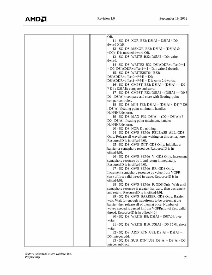
Revision 1.0 September 19, 2012
© 2012 Advanced Micro Devices, Inc. Proprietary 70
OR.
11 - SQ_DS_XOR_B32: DS[A] = DS[A] ^ D0;
dword XOR.
12 - SQ_DS_MSKOR_B32: DS[A] = (DS[A] &
~D0) | D1; masked dword OR.
13 - SQ_DS_WRITE_B32: DS[A] = D0; write
dword.
14 - SQ_DS_WRITE2_B32: DS[ADDR+offset0*4]
= D0; DS[ADDR+offset1*4] = D1; write 2 dwords.
15 - SQ_DS_WRITE2ST64_B32:
DS[ADDR+offset0*4*64] = D0;
DS[ADDR+offset1*4*64] = D1; write 2 dwords.
16 - SQ_DS_CMPST_B32: DS[A] = (DS[A] == D0
? D1 : DS[A]); compare and store.
17 - SQ_DS_CMPST_F32: DS[A] = (DS[A] == D0 ?
D1 : DS[A]); compare and store with floating-point
comparison rules.
18 - SQ_DS_MIN_F32: DS[A] = (DS[A] < D1) ? D0
: DS[A]; floating point minimum, handles
NaN/INF/denorm.
19 - SQ_DS_MAX_F32: DS[A] = (D0 > DS[A]) ?
D0 : DS[A]; floating point maximum, handles
NaN/INF/denorm.
20 - SQ_DS_NOP: Do nothing.
24 - SQ_DS_GWS_SEMA_RELEASE_ALL: GDS
Only. Release all wavefronts waiting on this semaphore.
ResourceID is in offset[4:0].
25 - SQ_DS_GWS_INIT: GDS Only. Initialize a
barrier or semaphore resource. ResourceID is in
offset[4:0].
26 - SQ_DS_GWS_SEMA_V: GDS Only. Increment
semaphore resource by 1 and return immediately.
ResourceID is in offset[4:0].
27 - SQ_DS_GWS_SEMA_BR: GDS Only.
Increment semaphore resource by value from VGPR
(src) of first valid thread in wave. ResourceID is in
offset[4:0].
28 - SQ_DS_GWS_SEMA_P: GDS Only. Wait until
semaphore resource is greater than zero, then decrement
and return. ResourceID is in offset[4:0].
29 - SQ_DS_GWS_BARRIER: GDS Only. Barrier
wait. Wait for enough wavefronts to be present at the
barrier, then release all of them at once. Number of
waves needed is passed in from VGPR(src) of first valid
thread. ResourceID is in offset[4:0].
30 - SQ_DS_WRITE_B8: DS[A] = D0[7:0]; byte
write.
31 - SQ_DS_WRITE_B16: DS[A] = D0[15:0]; short
write.
32 - SQ_DS_ADD_RTN_U32: DS[A] = DS[A] +
D0; integer add.
33 - SQ_DS_SUB_RTN_U32: DS[A] = DS[A] - D0;
integer subtract.

Revision 1.0 September 19, 2012
© 2012 Advanced Micro Devices, Inc. Proprietary 71
34 - SQ_DS_RSUB_RTN_U32: DS[A] = D0 -
DS[A]; integer reverse subtract.
35 - SQ_DS_INC_RTN_U32: DS[A] = (DS[A] >=
D0 ? 0 : DS[A] + 1); unsigned integer increment.
36 - SQ_DS_DEC_RTN_U32: DS[A] = (DS[A] == 0
|| DS[A] > D0 ? D0 : DS[A] - 1); unsigned integer
decrement.
37 - SQ_DS_MIN_RTN_I32: DS[A] = min(DS[A],
D0); signed integer mininum.
38 - SQ_DS_MAX_RTN_I32: DS[A] = max(DS[A],
D0); signed integer maximum.
39 - SQ_DS_MIN_RTN_U32: DS[A] = min(DS[A],
D0); unsigned integer minimum.
40 - SQ_DS_MAX_RTN_U32: DS[A] =
max(DS[A], D0); unsigned integer maximum.
41 - SQ_DS_AND_RTN_B32: DS[A] = DS[A] &
D0; dword AND.
42 - SQ_DS_OR_RTN_B32: DS[A] = DS[A] | D0;
dword OR.
43 - SQ_DS_XOR_RTN_B32: DS[A] = DS[A] ^
D0; dword XOR.
44 - SQ_DS_MSKOR_RTN_B32: DS[A] = (DS[A]
& ~D0) | D1; masked dword OR.
45 - SQ_DS_WRXCHG_RTN_B32: Write
exchange. Offset = {offset1,offset0}. A = ADDR+offset.
D=DS[Addr]. DS[Addr]=D0.
46 - SQ_DS_WRXCHG2_RTN_B32: Write
exchange 2 separate dwords.
47 - SQ_DS_WRXCHG2ST64_RTN_B32: Write
echange 2 dwords, stride 64.
48 - SQ_DS_CMPST_RTN_B32: DS[A] = (DS[A]
== D0 ? D1 : DS[A]); compare and store.
49 - SQ_DS_CMPST_RTN_F32: DS[A] = (DS[A]
== D0 ? D1 : DS[A]); compare and store with floating-
point comparison rules.
50 - SQ_DS_MIN_RTN_F32: DS[A] = (DS[A] <
D1) ? D0 : DS[A]; floating point minimum, handles
NaN/INF/denorm.
51 - SQ_DS_MAX_RTN_F32: DS[A] = (D0 >
DS[A]) ? D0 : DS[A]; floating point maximum, handles
NaN/INF/denorm.
52 - SQ_DS_WRAP_RTN_B32: DS[A] = (DS[A]
>= D0) ? DS[A] - D0 : DS[A] + D1.
53 - SQ_DS_SWIZZLE_B32: R =
swizzle(Data(vgpr), offset1:offset0). dword swizzle. no
data is written to LDS. see ds_opcodes.docx for details.
54 - SQ_DS_READ_B32: R = DS[A]; dword read.
55 - SQ_DS_READ2_B32: R =
DS[ADDR+offset0*4], R+1 = DS[ADDR+offset1*4].
Read 2 dwords.
56 - SQ_DS_READ2ST64_B32: R =
DS[ADDR+offset0*4*64], R+1 =
DS[ADDR+offset1*4*64]. Read 2 dwords.

Revision 1.0 September 19, 2012
© 2012 Advanced Micro Devices, Inc. Proprietary 72
57 - SQ_DS_READ_I8: R = signext(DS[A][7:0]};
signed byte read.
58 - SQ_DS_READ_U8: R = {24`h0,DS[A][7:0]};
unsigned byte read.
59 - SQ_DS_READ_I16: R = signext(DS[A][15:0]};
signed short read.
60 - SQ_DS_READ_U16: R = {16`h0,DS[A][15:0]};
unsigned short read.
61 - SQ_DS_CONSUME: LDS & GDS. Subtract
(count_bits(exec_mask)) from the value stored in DS
memory at (M0.base + instr_offset). Return the pre-
operation value to VGPRs.
62 - SQ_DS_APPEND: LDS & GDS. Add
(count_bits(exec_mask)) to the value stored in DS
memory at (M0.base + instr_offset). Return the pre-
operation value to VGPRs.
63 - SQ_DS_ORDERED_COUNT: GDS-only. Add
(count_bits(exec_mask)) to one of 4 dedicated ordered-
count counters (aka `packers`). Additional bits of
instr.offset field are overloaded to hold packer-id, `last`.
64 - SQ_DS_ADD_U64: DS[A] = DS[A] + D0; 64-
bit integer add.
65 - SQ_DS_SUB_U64: DS[A] = DS[A] - D0; 64-bit
integer subtract.
66 - SQ_DS_RSUB_U64: DS[A] = D0 - DS[A]; 64-
bit integer reverse subtract.
67 - SQ_DS_INC_U64: DS[A] = (DS[A] >= D0 ? 0 :
DS[A] + 1); unsigned 64-bit integer increment.
68 - SQ_DS_DEC_U64: DS[A] = (DS[A] == 0 ||
DS[A] > D0 ? D0 : DS[A] - 1); unsigned 64-bit integer
decrement.
69 - SQ_DS_MIN_I64: DS[A] = min(DS[A], D0);
signed 64-bit integer mininum.
70 - SQ_DS_MAX_I64: DS[A] = max(DS[A], D0);
signed 64-bit integer maximum.
71 - SQ_DS_MIN_U64: DS[A] = min(DS[A], D0);
unsigned 64-bit integer minimum.
72 - SQ_DS_MAX_U64: DS[A] = max(DS[A], D0);
unsigned 64-bit integer maximum.
73 - SQ_DS_AND_B64: DS[A] = DS[A] & D0;
qword AND.
74 - SQ_DS_OR_B64: DS[A] = DS[A] | D0; qword
OR.
75 - SQ_DS_XOR_B64: DS[A] = DS[A] ^ D0;
qword XOR.
76 - SQ_DS_MSKOR_B64: DS[A] = (DS[A] &
~D0) | D1; masked qword OR.
77 - SQ_DS_WRITE_B64: DS[A] = D0; write
qword.
78 - SQ_DS_WRITE2_B64: DS[ADDR+offset0*8]
= D0; DS[ADDR+offset1*8] = D1; write 2 qwords.
79 - SQ_DS_WRITE2ST64_B64:
DS[ADDR+offset0*8*64] = D0;
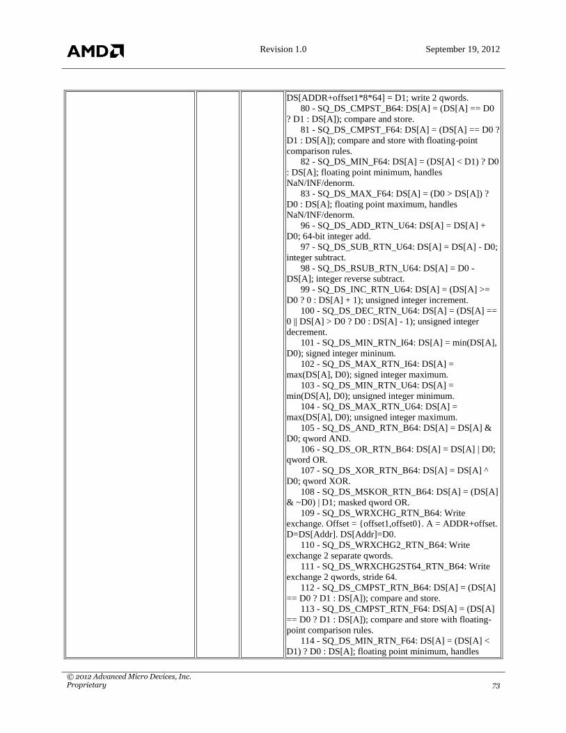
Revision 1.0 September 19, 2012
© 2012 Advanced Micro Devices, Inc. Proprietary 73
DS[ADDR+offset1*8*64] = D1; write 2 qwords.
80 - SQ_DS_CMPST_B64: DS[A] = (DS[A] == D0
? D1 : DS[A]); compare and store.
81 - SQ_DS_CMPST_F64: DS[A] = (DS[A] == D0 ?
D1 : DS[A]); compare and store with floating-point
comparison rules.
82 - SQ_DS_MIN_F64: DS[A] = (DS[A] < D1) ? D0
: DS[A]; floating point minimum, handles
NaN/INF/denorm.
83 - SQ_DS_MAX_F64: DS[A] = (D0 > DS[A]) ?
D0 : DS[A]; floating point maximum, handles
NaN/INF/denorm.
96 - SQ_DS_ADD_RTN_U64: DS[A] = DS[A] +
D0; 64-bit integer add.
97 - SQ_DS_SUB_RTN_U64: DS[A] = DS[A] - D0;
integer subtract.
98 - SQ_DS_RSUB_RTN_U64: DS[A] = D0 -
DS[A]; integer reverse subtract.
99 - SQ_DS_INC_RTN_U64: DS[A] = (DS[A] >=
D0 ? 0 : DS[A] + 1); unsigned integer increment.
100 - SQ_DS_DEC_RTN_U64: DS[A] = (DS[A] ==
0 || DS[A] > D0 ? D0 : DS[A] - 1); unsigned integer
decrement.
101 - SQ_DS_MIN_RTN_I64: DS[A] = min(DS[A],
D0); signed integer mininum.
102 - SQ_DS_MAX_RTN_I64: DS[A] =
max(DS[A], D0); signed integer maximum.
103 - SQ_DS_MIN_RTN_U64: DS[A] =
min(DS[A], D0); unsigned integer minimum.
104 - SQ_DS_MAX_RTN_U64: DS[A] =
max(DS[A], D0); unsigned integer maximum.
105 - SQ_DS_AND_RTN_B64: DS[A] = DS[A] &
D0; qword AND.
106 - SQ_DS_OR_RTN_B64: DS[A] = DS[A] | D0;
qword OR.
107 - SQ_DS_XOR_RTN_B64: DS[A] = DS[A] ^
D0; qword XOR.
108 - SQ_DS_MSKOR_RTN_B64: DS[A] = (DS[A]
& ~D0) | D1; masked qword OR.
109 - SQ_DS_WRXCHG_RTN_B64: Write
exchange. Offset = {offset1,offset0}. A = ADDR+offset.
D=DS[Addr]. DS[Addr]=D0.
110 - SQ_DS_WRXCHG2_RTN_B64: Write
exchange 2 separate qwords.
111 - SQ_DS_WRXCHG2ST64_RTN_B64: Write
exchange 2 qwords, stride 64.
112 - SQ_DS_CMPST_RTN_B64: DS[A] = (DS[A]
== D0 ? D1 : DS[A]); compare and store.
113 - SQ_DS_CMPST_RTN_F64: DS[A] = (DS[A]
== D0 ? D1 : DS[A]); compare and store with floating-
point comparison rules.
114 - SQ_DS_MIN_RTN_F64: DS[A] = (DS[A] <
D1) ? D0 : DS[A]; floating point minimum, handles

Revision 1.0 September 19, 2012
© 2012 Advanced Micro Devices, Inc. Proprietary 74
NaN/INF/denorm.
115 - SQ_DS_MAX_RTN_F64: DS[A] = (D0 >
DS[A]) ? D0 : DS[A]; floating point maximum, handles
NaN/INF/denorm.
118 - SQ_DS_READ_B64: R = DS[ADDR]. Read 1
dword.
119 - SQ_DS_READ2_B64: R =
DS[ADDR+offset0*8], R+1 = DS[ADDR+offset1*8].
Read 2 dwords.
120 - SQ_DS_READ2ST64_B64: R =
DS[ADDR+offset0*8*64], R+1 =
DS[ADDR+offset1*8*64]. Read 2 dwords.
126 - SQ_DS_CONDXCHG32_RTN_B64:
Conditional write exchange.
128 - SQ_DS_ADD_SRC2_U32: B = A +
4*(offset1[7] ? {A[31],A[31:17]} :
{offset1[6],offset1[6:0],offset0}). DS[A] = DS[A] +
DS[B]; uint add.
129 - SQ_DS_SUB_SRC2_U32: B = A +
4*(offset1[7] ? {A[31],A[31:17]} :
{offset1[6],offset1[6:0],offset0}). DS[A] = DS[A] -
DS[B]; uint subtract.
130 - SQ_DS_RSUB_SRC2_U32: B = A +
4*(offset1[7] ? {A[31],A[31:17]} :
{offset1[6],offset1[6:0],offset0}). DS[A] = DS[B] -
DS[A]; uint reverse subtract.
131 - SQ_DS_INC_SRC2_U32: B = A +
4*(offset1[7] ? {A[31],A[31:17]} :
{offset1[6],offset1[6:0],offset0}). DS[A] = (DS[A] >=
DS[B] ? 0 : DS[A] + 1); uint increment.
132 - SQ_DS_DEC_SRC2_U32: B = A +
4*(offset1[7] ? {A[31],A[31:17]} :
{offset1[6],offset1[6:0],offset0}). DS[A] = (DS[A] == 0
|| DS[A] > DS[B] ? DS[B] : DS[A] - 1); uint decrement.
133 - SQ_DS_MIN_SRC2_I32: B = A +
4*(offset1[7] ? {A[31],A[31:17]} :
{offset1[6],offset1[6:0],offset0}). DS[A] = min(DS[A],
DS[B]); int min.
134 - SQ_DS_MAX_SRC2_I32: B = A +
4*(offset1[7] ? {A[31],A[31:17]} :
{offset1[6],offset1[6:0],offset0}). DS[A] = max(DS[A],
DS[B]); int max.
135 - SQ_DS_MIN_SRC2_U32: B = A +
4*(offset1[7] ? {A[31],A[31:17]} :
{offset1[6],offset1[6:0],offset0}). DS[A] = min(DS[A],
DS[B]); uint min.
136 - SQ_DS_MAX_SRC2_U32: B = A +
4*(offset1[7] ? {A[31],A[31:17]} :
{offset1[6],offset1[6:0],offset0}). DS[A] = max(DS[A],
DS[B]); uint max.
137 - SQ_DS_AND_SRC2_B32: B = A +
4*(offset1[7] ? {A[31],A[31:17]} :
{offset1[6],offset1[6:0],offset0}). DS[A] = DS[A] &
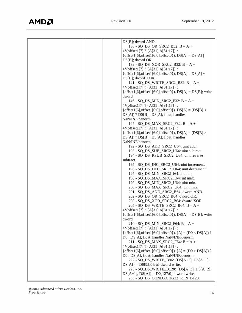
Revision 1.0 September 19, 2012
© 2012 Advanced Micro Devices, Inc. Proprietary 75
DS[B]; dword AND.
138 - SQ_DS_OR_SRC2_B32: B = A +
4*(offset1[7] ? {A[31],A[31:17]} :
{offset1[6],offset1[6:0],offset0}). DS[A] = DS[A] |
DS[B]; dword OR.
139 - SQ_DS_XOR_SRC2_B32: B = A +
4*(offset1[7] ? {A[31],A[31:17]} :
{offset1[6],offset1[6:0],offset0}). DS[A] = DS[A] ^
DS[B]; dword XOR.
141 - SQ_DS_WRITE_SRC2_B32: B = A +
4*(offset1[7] ? {A[31],A[31:17]} :
{offset1[6],offset1[6:0],offset0}). DS[A] = DS[B]; write
dword.
146 - SQ_DS_MIN_SRC2_F32: B = A +
4*(offset1[7] ? {A[31],A[31:17]} :
{offset1[6],offset1[6:0],offset0}). DS[A] = (DS[B] <
DS[A]) ? DS[B] : DS[A]; float, handles
NaN/INF/denorm.
147 - SQ_DS_MAX_SRC2_F32: B = A +
4*(offset1[7] ? {A[31],A[31:17]} :
{offset1[6],offset1[6:0],offset0}). DS[A] = (DS[B] >
DS[A]) ? DS[B] : DS[A]; float, handles
NaN/INF/denorm.
192 - SQ_DS_ADD_SRC2_U64: uint add.
193 - SQ_DS_SUB_SRC2_U64: uint subtract.
194 - SQ_DS_RSUB_SRC2_U64: uint reverse
subtract.
195 - SQ_DS_INC_SRC2_U64: uint increment.
196 - SQ_DS_DEC_SRC2_U64: uint decrement.
197 - SQ_DS_MIN_SRC2_I64: int min.
198 - SQ_DS_MAX_SRC2_I64: int max.
199 - SQ_DS_MIN_SRC2_U64: uint min.
200 - SQ_DS_MAX_SRC2_U64: uint max.
201 - SQ_DS_AND_SRC2_B64: dword AND.
202 - SQ_DS_OR_SRC2_B64: dword OR.
203 - SQ_DS_XOR_SRC2_B64: dword XOR.
205 - SQ_DS_WRITE_SRC2_B64: B = A +
4*(offset1[7] ? {A[31],A[31:17]} :
{offset1[6],offset1[6:0],offset0}). DS[A] = DS[B]; write
qword.
210 - SQ_DS_MIN_SRC2_F64: B = A +
4*(offset1[7] ? {A[31],A[31:17]} :
{offset1[6],offset1[6:0],offset0}). [A] = (D0 < DS[A]) ?
D0 : DS[A]; float, handles NaN/INF/denorm.
211 - SQ_DS_MAX_SRC2_F64: B = A +
4*(offset1[7] ? {A[31],A[31:17]} :
{offset1[6],offset1[6:0],offset0}). [A] = (D0 > DS[A]) ?
D0 : DS[A]; float, handles NaN/INF/denorm.
222 - SQ_DS_WRITE_B96: {DS[A+2], DS[A+1],
DS[A]} = D0[95:0]; tri-dword write.
223 - SQ_DS_WRITE_B128: {DS[A+3], DS[A+2],
DS[A+1], DS[A]} = D0[127:0]; qword write.
253 - SQ_DS_CONDXCHG32_RTN_B128:

Revision 1.0 September 19, 2012
© 2012 Advanced Micro Devices, Inc. Proprietary 76
Conditional write exchange.
254 - SQ_DS_READ_B96: tri-dword read.
255 - SQ_DS_READ_B128: qword read.
ENCODING 31:26 none Encoding.
POSSIBLE VALUES:
54 - SQ_ENC_DS_FIELD: Must be set to this value.
SQ_UC:SQ_DS_1 · [R/W] · 32 bits · Access: 32 · GpuF0MMReg:0x8dfc
DESCRIPTION: LDS or GDS operation - second word.
Field Name Bits Default Description
ADDR 7:0 none source lds address vgpr
POSSIBLE VALUES:
00 - SQ_VGPR: Vector GPR 0. Increment from here
for additional GPRs. There are NUM_VGPR VGPRs in
total.
DATA0 15:8 none source data 0
POSSIBLE VALUES:
00 - SQ_VGPR: Vector GPR 0. Increment from here
for additional GPRs. There are NUM_VGPR VGPRs in
total.
DATA1 23:16 none source data 1
POSSIBLE VALUES:
00 - SQ_VGPR: Vector GPR 0. Increment from here
for additional GPRs. There are NUM_VGPR VGPRs in
total.
VDST 31:24 none dest vgpr
POSSIBLE VALUES:
00 - SQ_VGPR: Vector GPR 0. Increment from here
for additional GPRs. There are NUM_VGPR VGPRs in
total.
SQ_UC:SQ_EXP_0 · [R/W] · 32 bits · Access: 32 · GpuF0MMReg:0x8dfc
DESCRIPTION: Export, first word.
Field Name Bits Default Description
EN 3:0 none En[0] is red or x, en[3] is alpha or w. Compr. export:
enables for half-dword export; EN[0] for low 16 bits of
VSRC0, EN[1] for high 16 bits of VSRC0, EN[2] for
low 16 bits of VSRC1, EN[3] for high 16 bits of VSRC1.
Non-float16: enables for VSRCs, EN[N] for VSRC[N].
TGT 9:4 none Export target based on the enumeration below.
POSSIBLE VALUES:
00 - SQ_EXP_MRT: Output to colour MRT 0.
Increment from here for additional MRTs. There are
EXP_NUM_MRT MRTs in total.
08 - SQ_EXP_MRTZ: Output to Z.
09 - SQ_EXP_NULL: Output to NULL.
12 - SQ_EXP_POS: Output to position 0. Increment
from here for additional positions. There are

Revision 1.0 September 19, 2012
© 2012 Advanced Micro Devices, Inc. Proprietary 77
EXP_NUM_POS positions in total.
32 - SQ_EXP_PARAM: Output to parameter 0.
Increment from here for additional parameters. There are
EXP_NUM_PARAM parameters in total.
COMPR 10 none Boolean. If true, data is exported in float16 format;If
false, data is 32 bit.
DONE 11 none If set, this is the last export of a given type. If this is set
for a colour export (PS only), then the valid mask must
be present in the EXEC register.
VM 12 none Mask contains valid-mask when set; otherwise mask is
just write-mask. Used only for pixel(mrt) exports.
ENCODING 31:26 none Encoding.
POSSIBLE VALUES:
62 - SQ_ENC_EXP_FIELD: Must be set to this
value.
SQ_UC:SQ_EXP_1 · [R/W] · 32 bits · Access: 32 · GpuF0MMReg:0x8dfc
DESCRIPTION: Export, second word.
Field Name Bits Default Description
VSRC0 7:0 none VGPR of the first data to export.
POSSIBLE VALUES:
00 - SQ_VGPR: Vector GPR 0. Increment from here
for additional GPRs. There are NUM_VGPR VGPRs in
total.
VSRC1 15:8 none VGPR of the second data to export.
POSSIBLE VALUES:
00 - SQ_VGPR: Vector GPR 0. Increment from here
for additional GPRs. There are NUM_VGPR VGPRs in
total.
VSRC2 23:16 none VGPR of the third data to export.
POSSIBLE VALUES:
00 - SQ_VGPR: Vector GPR 0. Increment from here
for additional GPRs. There are NUM_VGPR VGPRs in
total.
VSRC3 31:24 none VGPR of the fourth data to export.
POSSIBLE VALUES:
00 - SQ_VGPR: Vector GPR 0. Increment from here
for additional GPRs. There are NUM_VGPR VGPRs in
total.
SQ_UC:SQ_FLAT_0 · [R/W] · 32 bits · Access: 32 · GpuF0MMReg:0x8dfc
DESCRIPTION: FLAT, first word.
Field Name Bits Default Description
GLC 16 none If set, operation is globally coherent.
SLC 17 none System Level Coherent.
OP 24:18 none Opcode.
POSSIBLE VALUES:
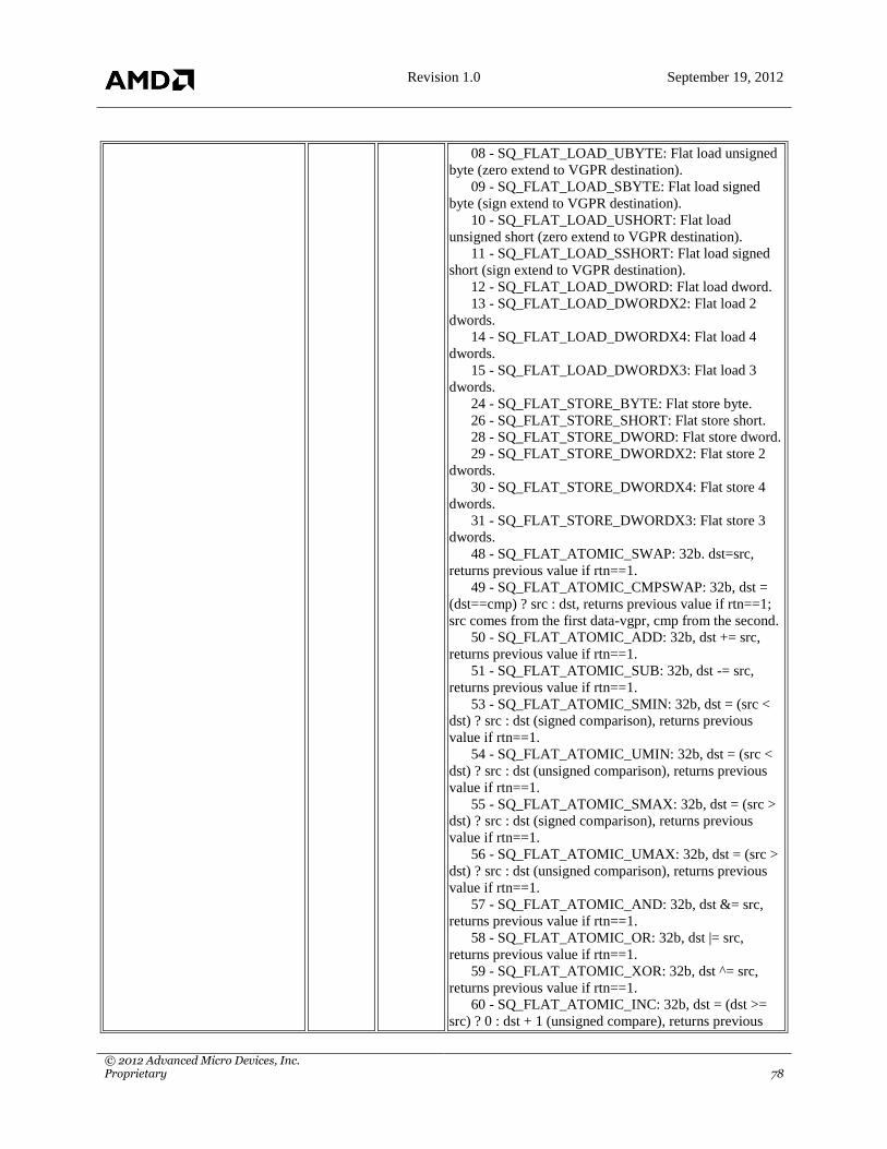
Revision 1.0 September 19, 2012
© 2012 Advanced Micro Devices, Inc. Proprietary 78
08 - SQ_FLAT_LOAD_UBYTE: Flat load unsigned
byte (zero extend to VGPR destination).
09 - SQ_FLAT_LOAD_SBYTE: Flat load signed
byte (sign extend to VGPR destination).
10 - SQ_FLAT_LOAD_USHORT: Flat load
unsigned short (zero extend to VGPR destination).
11 - SQ_FLAT_LOAD_SSHORT: Flat load signed
short (sign extend to VGPR destination).
12 - SQ_FLAT_LOAD_DWORD: Flat load dword.
13 - SQ_FLAT_LOAD_DWORDX2: Flat load 2
dwords.
14 - SQ_FLAT_LOAD_DWORDX4: Flat load 4
dwords.
15 - SQ_FLAT_LOAD_DWORDX3: Flat load 3
dwords.
24 - SQ_FLAT_STORE_BYTE: Flat store byte.
26 - SQ_FLAT_STORE_SHORT: Flat store short.
28 - SQ_FLAT_STORE_DWORD: Flat store dword.
29 - SQ_FLAT_STORE_DWORDX2: Flat store 2
dwords.
30 - SQ_FLAT_STORE_DWORDX4: Flat store 4
dwords.
31 - SQ_FLAT_STORE_DWORDX3: Flat store 3
dwords.
48 - SQ_FLAT_ATOMIC_SWAP: 32b. dst=src,
returns previous value if rtn==1.
49 - SQ_FLAT_ATOMIC_CMPSWAP: 32b, dst =
(dst==cmp) ? src : dst, returns previous value if rtn==1;
src comes from the first data-vgpr, cmp from the second.
50 - SQ_FLAT_ATOMIC_ADD: 32b, dst += src,
returns previous value if rtn==1.
51 - SQ_FLAT_ATOMIC_SUB: 32b, dst -= src,
returns previous value if rtn==1.
53 - SQ_FLAT_ATOMIC_SMIN: 32b, dst = (src <
dst) ? src : dst (signed comparison), returns previous
value if rtn==1.
54 - SQ_FLAT_ATOMIC_UMIN: 32b, dst = (src <
dst) ? src : dst (unsigned comparison), returns previous
value if rtn==1.
55 - SQ_FLAT_ATOMIC_SMAX: 32b, dst = (src >
dst) ? src : dst (signed comparison), returns previous
value if rtn==1.
56 - SQ_FLAT_ATOMIC_UMAX: 32b, dst = (src >
dst) ? src : dst (unsigned comparison), returns previous
value if rtn==1.
57 - SQ_FLAT_ATOMIC_AND: 32b, dst &= src,
returns previous value if rtn==1.
58 - SQ_FLAT_ATOMIC_OR: 32b, dst |= src,
returns previous value if rtn==1.
59 - SQ_FLAT_ATOMIC_XOR: 32b, dst ^= src,
returns previous value if rtn==1.
60 - SQ_FLAT_ATOMIC_INC: 32b, dst = (dst >=
src) ? 0 : dst + 1 (unsigned compare), returns previous

Revision 1.0 September 19, 2012
© 2012 Advanced Micro Devices, Inc. Proprietary 79
value if rtn==1.
61 - SQ_FLAT_ATOMIC_DEC: 32b, dst = ((dst==0
|| (dst > src)) ? src : dst - 1 (unsigned compare), returns
previous value if rtn==1.
62 - SQ_FLAT_ATOMIC_FCMPSWAP: 32b, dst =
(dst == cmp) ? src : dst, returns previous value if rtn==1.
Floating point compare-swap handles NaN/INF/denorm
in the comparison. Input src comes from the first data-
vgpr, cmp from the second.
63 - SQ_FLAT_ATOMIC_FMIN: 32b, dst = (src <
dst) ? src : dst, returns previous value if rtn==1. Floating
point compare handles NaN/INF/denorm.
64 - SQ_FLAT_ATOMIC_FMAX: 32b, dst = (src >
dst) ? src : dst, returns previous value if rtn==1. Floating
point compare handles NaN/INF/denorm.
80 - SQ_FLAT_ATOMIC_SWAP_X2: 64b, dst=src,
returns previous value if rtn==1
81 - SQ_FLAT_ATOMIC_CMPSWAP_X2: 64b, dst
= (dst==cmp) ? src : dst, returns previous value if
rtn==1; src comes from the first two data-vgprs, cmp
from the second two.
82 - SQ_FLAT_ATOMIC_ADD_X2: 64b, dst +=
src, returns previous value if rtn==1.
83 - SQ_FLAT_ATOMIC_SUB_X2: 64b, dst -= src,
returns previous value if rtn==1.
85 - SQ_FLAT_ATOMIC_SMIN_X2: 64b, dst = (src
< dst) ? src : dst (signed compare), returns previous value
if rtn==1.
86 - SQ_FLAT_ATOMIC_UMIN_X2: 64b, dst =
(src < dst) ? src : dst (unsigned compare), returns
previous value if rtn==1.
87 - SQ_FLAT_ATOMIC_SMAX_X2: 64b, dst =
(src > dst) ? src : dst (signed compare), returns previous
value if rtn==1.
88 - SQ_FLAT_ATOMIC_UMAX_X2: 64b, dst =
(src > dst) ? src : dst (unsigned compare), returns
previous value if rtn==1.
89 - SQ_FLAT_ATOMIC_AND_X2: 64b, dst &=
src, returns previous value if rtn==1.
90 - SQ_FLAT_ATOMIC_OR_X2: 64b, dst |= src,
returns previous value if rtn==1.
91 - SQ_FLAT_ATOMIC_XOR_X2: 64b, dst ^= src,
returns previous value if rtn==1.
92 - SQ_FLAT_ATOMIC_INC_X2: 64b, dst = (dst
>= src) ? 0 : dst + 1 (unsigned compare), returns previous
value if rtn==1.
93 - SQ_FLAT_ATOMIC_DEC_X2: 64b, dst =
((dst==0 || (dst > src)) ? src : dst - 1 (unsigned compare),
returns previous value if rtn==1.
94 - SQ_FLAT_ATOMIC_FCMPSWAP_X2: 64b,
dst = (dst == cmp) ? src : dst, returns previous value if
rtn==1. Double compare-swap, handles
NaN/INF/denorm. The src input comes from the first two

Revision 1.0 September 19, 2012
© 2012 Advanced Micro Devices, Inc. Proprietary 80
data-vgprs, cmp from the second two.
95 - SQ_FLAT_ATOMIC_FMIN_X2: 64b, dst = (src
< dst) ? src : dst, returns previous value if rtn==1. Double
compare handles NaN/INF/denorm.
96 - SQ_FLAT_ATOMIC_FMAX_X2: 64b, dst =
(src > dst) ? src : dst, returns previous value if rtn==1.
Double compare handles NaN/INF/denorm.
ENCODING 31:26 none Encoding.
POSSIBLE VALUES:
55 - SQ_ENC_FLAT_FIELD: Must be set to this
value.
SQ_UC:SQ_FLAT_1 · [R/W] · 32 bits · Access: 32 · GpuF0MMReg:0x8dfc
DESCRIPTION: FLAT, second word.
Field Name Bits Default Description
ADDR 7:0 none source flat address vgpr
POSSIBLE VALUES:
00 - SQ_VGPR: Vector GPR 0. Increment from here
for additional GPRs. There are NUM_VGPR VGPRs in
total.
DATA 15:8 none source data
POSSIBLE VALUES:
00 - SQ_VGPR: Vector GPR 0. Increment from here
for additional GPRs. There are NUM_VGPR VGPRs in
total.
TFE 23 none Texture Fail Enable (for partially resident textures).
VDST 31:24 none dest vgpr
POSSIBLE VALUES:
00 - SQ_VGPR: Vector GPR 0. Increment from here
for additional GPRs. There are NUM_VGPR VGPRs in
total.
SQ_UC:SQ_MIMG_0 · [R/W] · 32 bits · Access: 32 · GpuF0MMReg:0x8dfc
DESCRIPTION: Image memory buffer operation. First word.
Field Name Bits Default Description
DMASK 11:8 none Enable mask for image read/write data components.
bit0=red, 1=green, 2=blue, 3=alpha. At least 1 bit must
be on. Data is assumed to be packed into consecutive
VGPRs.
UNORM 12 none Force address to be un-normalized regardless of texture
sampler setting. Must be set to 1 for image store and
atomic operations.
GLC 13 none If set, operation is globally coherent.
DA 14 none Declare Array: 1=shader declared this texture to be an
array and SH always sends array-index (slice#) to TA;
0=shader declared non-array type and will never send out
array-index (slice#). TA will assume slice# is zero when
it doesn`t receive one.

Revision 1.0 September 19, 2012
© 2012 Advanced Micro Devices, Inc. Proprietary 81
R128 15 none Texture resource size: 1=128b, 0=256b
TFE 16 none Texture Fail Enable (for partially resident textures).
LWE 17 none LOD Warning Enable (for partially resident textures).
OP 24:18 none Opcode.
POSSIBLE VALUES:
00 - SQ_IMAGE_LOAD: Image memory load with
format conversion specified in T#. no sampler.
01 - SQ_IMAGE_LOAD_MIP: Image memory load
with user-supplied mip level. no sampler.
02 - SQ_IMAGE_LOAD_PCK: Image memory load
with no format conversion. no sampler.
03 - SQ_IMAGE_LOAD_PCK_SGN: Image
memory load with with no format conversion and sign
extension. no sampler.
04 - SQ_IMAGE_LOAD_MIP_PCK: Image memory
load with user-supplied mip level, no format conversion.
no sampler.
05 - SQ_IMAGE_LOAD_MIP_PCK_SGN: Image
memory load with user-supplied mip level, no format
conversion and with sign extension. no sampler.
08 - SQ_IMAGE_STORE: Image memory store with
format conversion specified in T#. no sampler.
09 - SQ_IMAGE_STORE_MIP: Image memory
store with format conversion specified in T# to user
specified mip level. no sampler.
10 - SQ_IMAGE_STORE_PCK: Image memory
store of packed data without format conversion . no
sampler.
11 - SQ_IMAGE_STORE_MIP_PCK: Image
memory store of packed data without format conversion
to user-supplied mip level. no sampler.
14 - SQ_IMAGE_GET_RESINFO: return resource
info. no sampler.
15 - SQ_IMAGE_ATOMIC_SWAP: dst=src, returns
previous value if glc==1
16 - SQ_IMAGE_ATOMIC_CMPSWAP: dst =
(dst==cmp) ? src : dst. returns previous value if glc==1
17 - SQ_IMAGE_ATOMIC_ADD: dst += src.
returns previous value if glc==1
18 - SQ_IMAGE_ATOMIC_SUB: dst -= src. returns
previous value if glc==1
20 - SQ_IMAGE_ATOMIC_SMIN: dst = (src < dst)
? src : dst (signed). returns previous value if glc==1
21 - SQ_IMAGE_ATOMIC_UMIN: dst = (src < dst)
? src : dst (unsigned). returns previous value if glc==1
22 - SQ_IMAGE_ATOMIC_SMAX: dst = (src > dst)
? src : dst (signed). returns previous value if glc==1
23 - SQ_IMAGE_ATOMIC_UMAX: dst = (src >
dst) ? src : dst (unsigned). returns previous value if
glc==1
24 - SQ_IMAGE_ATOMIC_AND: dst &= src.
returns previous value if glc==1
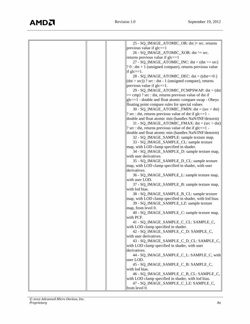
Revision 1.0 September 19, 2012
© 2012 Advanced Micro Devices, Inc. Proprietary 82
25 - SQ_IMAGE_ATOMIC_OR: dst |= src. returns
previous value if glc==1
26 - SQ_IMAGE_ATOMIC_XOR: dst ^= src.
returns previous value if glc==1
27 - SQ_IMAGE_ATOMIC_INC: dst = (dst >= src)
? 0 : dst + 1 (unsigned compare), returns previous value
if glc==1.
28 - SQ_IMAGE_ATOMIC_DEC: dst = ((dst==0 ||
(dst > src)) ? src : dst - 1 (unsigned compare), returns
previous value if glc==1.
29 - SQ_IMAGE_ATOMIC_FCMPSWAP: dst = (dst
== cmp) ? src : dst, returns previous value of dst if
glc==1 - double and float atomic compare swap - Obeys
floating point compare rules for special values
30 - SQ_IMAGE_ATOMIC_FMIN: dst = (src < dst)
? src : dst, returns previous value of dst if glc==1 -
double and float atomic min (handles NaN/INF/denorm)
31 - SQ_IMAGE_ATOMIC_FMAX: dst = (src > dst)
? src : dst, returns previous value of dst if glc==1 -
double and float atomic min (handles NaN/INF/denorm)
32 - SQ_IMAGE_SAMPLE: sample texture map.
33 - SQ_IMAGE_SAMPLE_CL: sample texture
map, with LOD clamp specified in shader.
34 - SQ_IMAGE_SAMPLE_D: sample texture map,
with user derivatives
35 - SQ_IMAGE_SAMPLE_D_CL: sample texture
map, with LOD clamp specified in shader, with user
derivatives.
36 - SQ_IMAGE_SAMPLE_L: sample texture map,
with user LOD.
37 - SQ_IMAGE_SAMPLE_B: sample texture map,
with lod bias.
38 - SQ_IMAGE_SAMPLE_B_CL: sample texture
map, with LOD clamp specified in shader, with lod bias.
39 - SQ_IMAGE_SAMPLE_LZ: sample texture
map, from level 0.
40 - SQ_IMAGE_SAMPLE_C: sample texture map,
with PCF.
41 - SQ_IMAGE_SAMPLE_C_CL: SAMPLE_C,
with LOD clamp specified in shader.
42 - SQ_IMAGE_SAMPLE_C_D: SAMPLE_C,
with user derivatives.
43 - SQ_IMAGE_SAMPLE_C_D_CL: SAMPLE_C,
with LOD clamp specified in shader, with user
derivatives.
44 - SQ_IMAGE_SAMPLE_C_L: SAMPLE_C, with
user LOD.
45 - SQ_IMAGE_SAMPLE_C_B: SAMPLE_C,
with lod bias.
46 - SQ_IMAGE_SAMPLE_C_B_CL: SAMPLE_C,
with LOD clamp specified in shader, with lod bias.
47 - SQ_IMAGE_SAMPLE_C_LZ: SAMPLE_C,
from level 0.

Revision 1.0 September 19, 2012
© 2012 Advanced Micro Devices, Inc. Proprietary 83
48 - SQ_IMAGE_SAMPLE_O: sample texture map,
with user offsets.
49 - SQ_IMAGE_SAMPLE_CL_O: SAMPLE_O
with LOD clamp specified in shader.
50 - SQ_IMAGE_SAMPLE_D_O: SAMPLE_O,
with user derivatives.
51 - SQ_IMAGE_SAMPLE_D_CL_O: SAMPLE_O,
with LOD clamp specified in shader, with user
derivatives.
52 - SQ_IMAGE_SAMPLE_L_O: SAMPLE_O,
with user LOD.
53 - SQ_IMAGE_SAMPLE_B_O: SAMPLE_O,
with lod bias.
54 - SQ_IMAGE_SAMPLE_B_CL_O: SAMPLE_O,
with LOD clamp specified in shader, with lod bias.
55 - SQ_IMAGE_SAMPLE_LZ_O: SAMPLE_O,
from level 0.
56 - SQ_IMAGE_SAMPLE_C_O: SAMPLE_C with
user specified offsets.
57 - SQ_IMAGE_SAMPLE_C_CL_O:
SAMPLE_C_O, with LOD clamp specified in shader.
58 - SQ_IMAGE_SAMPLE_C_D_O:
SAMPLE_C_O, with user derivatives.
59 - SQ_IMAGE_SAMPLE_C_D_CL_O:
SAMPLE_C_O, with LOD clamp specified in shader,
with user derivatives.
60 - SQ_IMAGE_SAMPLE_C_L_O:
SAMPLE_C_O, with user LOD.
61 - SQ_IMAGE_SAMPLE_C_B_O:
SAMPLE_C_O, with lod bias.
62 - SQ_IMAGE_SAMPLE_C_B_CL_O:
SAMPLE_C_O, with LOD clamp specified in shader,
with lod bias.
63 - SQ_IMAGE_SAMPLE_C_LZ_O:
SAMPLE_C_O, from level 0.
64 - SQ_IMAGE_GATHER4: gather 4 single
component elements (2x2).
65 - SQ_IMAGE_GATHER4_CL: gather 4 single
component elements (2x2) with user LOD clamp.
68 - SQ_IMAGE_GATHER4_L: gather 4 single
component elements (2x2) with user LOD.
69 - SQ_IMAGE_GATHER4_B: gather 4 single
component elements (2x2) with user bias.
70 - SQ_IMAGE_GATHER4_B_CL: gather 4 single
component elements (2x2) with user bias and clamp.
71 - SQ_IMAGE_GATHER4_LZ: gather 4 single
component elements (2x2) at level 0.
72 - SQ_IMAGE_GATHER4_C: gather 4 single
component elements (2x2) with PCF.
73 - SQ_IMAGE_GATHER4_C_CL: gather 4 single
component elements (2x2) with user LOD clamp and
PCF.
76 - SQ_IMAGE_GATHER4_C_L: gather 4 single

Revision 1.0 September 19, 2012
© 2012 Advanced Micro Devices, Inc. Proprietary 84
component elements (2x2) with user LOD and PCF.
77 - SQ_IMAGE_GATHER4_C_B: gather 4 single
component elements (2x2) with user bias and PCF.
78 - SQ_IMAGE_GATHER4_C_B_CL: gather 4
single component elements (2x2) with user bias, clamp
and PCF.
79 - SQ_IMAGE_GATHER4_C_LZ: gather 4 single
component elements (2x2) at level 0, with PCF.
80 - SQ_IMAGE_GATHER4_O: GATHER4, with
user offsets.
81 - SQ_IMAGE_GATHER4_CL_O:
GATHER4_CL, with user offsets.
84 - SQ_IMAGE_GATHER4_L_O: GATHER4_L,
with user offsets.
85 - SQ_IMAGE_GATHER4_B_O: GATHER4_B,
with user offsets.
86 - SQ_IMAGE_GATHER4_B_CL_O:
GATHER4_B_CL, with user offsets.
87 - SQ_IMAGE_GATHER4_LZ_O:
GATHER4_LZ, with user offsets.
88 - SQ_IMAGE_GATHER4_C_O: GATHER4_C,
with user offsets.
89 - SQ_IMAGE_GATHER4_C_CL_O:
GATHER4_C_CL, with user offsets.
92 - SQ_IMAGE_GATHER4_C_L_O:
GATHER4_C_L, with user offsets.
93 - SQ_IMAGE_GATHER4_C_B_O:
GATHER4_B, with user offsets.
94 - SQ_IMAGE_GATHER4_C_B_CL_O:
GATHER4_B_CL, with user offsets.
95 - SQ_IMAGE_GATHER4_C_LZ_O:
GATHER4_C_LZ, with user offsets.
96 - SQ_IMAGE_GET_LOD: Return calculated
LOD.
104 - SQ_IMAGE_SAMPLE_CD: sample texture
map, with user derivatives (LOD per quad)
105 - SQ_IMAGE_SAMPLE_CD_CL: sample
texture map, with LOD clamp specified in shader, with
user derivatives (LOD per quad).
106 - SQ_IMAGE_SAMPLE_C_CD: SAMPLE_C,
with user derivatives (LOD per quad).
107 - SQ_IMAGE_SAMPLE_C_CD_CL:
SAMPLE_C, with LOD clamp specified in shader, with
user derivatives (LOD per quad).
108 - SQ_IMAGE_SAMPLE_CD_O: SAMPLE_O,
with user derivatives (LOD per quad).
109 - SQ_IMAGE_SAMPLE_CD_CL_O:
SAMPLE_O, with LOD clamp specified in shader, with
user derivatives (LOD per quad).
110 - SQ_IMAGE_SAMPLE_C_CD_O:
SAMPLE_C_O, with user derivatives (LOD per quad).
111 - SQ_IMAGE_SAMPLE_C_CD_CL_O:
SAMPLE_C_O, with LOD clamp specified in shader,

Revision 1.0 September 19, 2012
© 2012 Advanced Micro Devices, Inc. Proprietary 85
with user derivatives (LOD per quad).
126 - SQ_IMAGE_RSRC256: DO NOT USE - for
sq_ta_cmd bus only.
127 - SQ_IMAGE_SAMPLER: DO NOT USE - for
sq_ta_cmd bus only.
SLC 25 none System Level Coherent.
ENCODING 31:26 none Encoding.
POSSIBLE VALUES:
60 - SQ_ENC_MIMG_FIELD: Must be set to this
value.
SQ_UC:SQ_MIMG_1 · [R/W] · 32 bits · Access: 32 · GpuF0MMReg:0x8dfc
DESCRIPTION: Image memory buffer operation. Second word.
Field Name Bits Default Description
VADDR 7:0 none Address source - may carry an offset or an index.
POSSIBLE VALUES:
00 - SQ_VGPR: Vector GPR 0. Increment from here
for additional GPRs. There are NUM_VGPR VGPRs in
total.
VDATA 15:8 none Vector GPR to write result to.
POSSIBLE VALUES:
00 - SQ_VGPR: Vector GPR 0. Increment from here
for additional GPRs. There are NUM_VGPR VGPRs in
total.
SRSRC 20:16 none Scalar GPR that specifies the resource constant, in units
of 4 SGPRs.
SSAMP 25:21 none Scalar GPR that specifies the sampler constant, in units
of 4 SGPRs.
SQ_UC:SQ_MTBUF_0 · [R/W] · 32 bits · Access: 32 · GpuF0MMReg:0x8dfc
DESCRIPTION: Typed memory buffer operation. First word.
Field Name Bits Default Description
OFFSET 11:0 none Unsigned byte offset. Only used when OFFEN = 0.
OFFEN 12 none If set, send VADDR as an offset. If unset, send the
instruction offset stored in OFFSET. Only one of these
offsets may be sent.
IDXEN 13 none If set, send VADDR as an index. If unset, treat the index
as zero.
GLC 14 none If set, operation is globally coherent.
ADDR64 15 none If set, buffer address is 64-bits (base & size in resource is
ignored).
OP 18:16 none opcode: read/write and x,xy,xyz,xyzw
POSSIBLE VALUES:
00 - SQ_TBUFFER_LOAD_FORMAT_X: Typed
buffer load 1 dword with format conversion
01 - SQ_TBUFFER_LOAD_FORMAT_XY: Typed
buffer load 2 dwords with format conversion
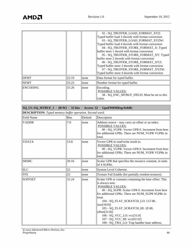
Revision 1.0 September 19, 2012
© 2012 Advanced Micro Devices, Inc. Proprietary 86
02 - SQ_TBUFFER_LOAD_FORMAT_XYZ:
Typed buffer load 3 dwords with format conversion
03 - SQ_TBUFFER_LOAD_FORMAT_XYZW:
Typed buffer load 4 dwords with format conversion
04 - SQ_TBUFFER_STORE_FORMAT_X: Typed
buffer store 1 dword with format conversion
05 - SQ_TBUFFER_STORE_FORMAT_XY: Typed
buffer store 2 dwords with format conversion
06 - SQ_TBUFFER_STORE_FORMAT_XYZ:
Typed buffer store 3 dwords with format conversion
07 - SQ_TBUFFER_STORE_FORMAT_XYZW:
Typed buffer store 4 dwords with format conversion
DFMT 22:19 none Data format for typed buffer.
NFMT 25:23 none Number format for typed buffer.
ENCODING 31:26 none Encoding.
POSSIBLE VALUES:
58 - SQ_ENC_MTBUF_FIELD: Must be set to this
value.
SQ_UC:SQ_MTBUF_1 · [R/W] · 32 bits · Access: 32 · GpuF0MMReg:0x8dfc
DESCRIPTION: Typed memory buffer operation. Second word.
Field Name Bits Default Description
VADDR 7:0 none Address source - may carry an offset or an index.
POSSIBLE VALUES:
00 - SQ_VGPR: Vector GPR 0. Increment from here
for additional GPRs. There are NUM_VGPR VGPRs in
total.
VDATA 15:8 none Vector GPR to read/write result to.
POSSIBLE VALUES:
00 - SQ_VGPR: Vector GPR 0. Increment from here
for additional GPRs. There are NUM_VGPR VGPRs in
total.
SRSRC 20:16 none Scalar GPR that specifies the resource constant, in units
of 4 SGPRs.
SLC 22 none System Level Coherent.
TFE 23 none Texture Fail Enable (for partially resident textures).
SOFFSET 31:24 none Scalar GPR or constant containing the base offset. This
is always sent.
POSSIBLE VALUES:
00 - SQ_SGPR: Scalar GPR 0. Increment from here
for additional GPRs. There are NUM_SGPR SGPRs in
total.
104 - SQ_FLAT_SCRATCH_LO: {13`d0,
size[18:0]}
105 - SQ_FLAT_SCRATCH_HI: {8`d0,
offset[31:8]}
106 - SQ_VCC_LO: vcc[31:0]
107 - SQ_VCC_HI: vcc[63:32]
108 - SQ_TBA_LO: Trap handler base address,

Revision 1.0 September 19, 2012
© 2012 Advanced Micro Devices, Inc. Proprietary 87
[31:0]
109 - SQ_TBA_HI: Trap handler base address,
[63:32]
110 - SQ_TMA_LO: Pointer to data in memory used
by trap handler.
111 - SQ_TMA_HI: Pointer to data in memory used
by trap handler.
112 - SQ_TTMP0: Trap handler temps (privileged).
Increment from here for additional TTMPs. There are
NUM_TTMP TTMPs in total. {TTMP1,TTMP0} =
PC_save{hi,lo}.
113 - SQ_TTMP1: Trap handler temps (privileged).
114 - SQ_TTMP2: Trap handler temps (privileged).
115 - SQ_TTMP3: Trap handler temps (privileged).
116 - SQ_TTMP4: Trap handler temps (privileged).
117 - SQ_TTMP5: Trap handler temps (privileged).
118 - SQ_TTMP6: Trap handler temps (privileged).
119 - SQ_TTMP7: Trap handler temps (privileged).
120 - SQ_TTMP8: Trap handler temps (privileged).
121 - SQ_TTMP9: Trap handler temps (privileged).
122 - SQ_TTMP10: Trap handler temps (privileged).
123 - SQ_TTMP11: Trap handler temps (privileged).
124 - SQ_M0: Special register used to hold
LDS/GDS addresses, relative indices, and send-messsage
values.
126 - SQ_EXEC_LO: exec[31:0]
127 - SQ_EXEC_HI: exec[63:32]
128 - SQ_SRC_0: 0
129 - SQ_SRC_1_INT: 1 (integer)
130 - SQ_SRC_2_INT: 2 (integer)
131 - SQ_SRC_3_INT: 3 (integer)
132 - SQ_SRC_4_INT: 4 (integer)
133 - SQ_SRC_5_INT: 5 (integer)
134 - SQ_SRC_6_INT: 6 (integer)
135 - SQ_SRC_7_INT: 7 (integer)
136 - SQ_SRC_8_INT: 8 (integer)
137 - SQ_SRC_9_INT: 9 (integer)
138 - SQ_SRC_10_INT: 10 (integer)
139 - SQ_SRC_11_INT: 11 (integer)
140 - SQ_SRC_12_INT: 12 (integer)
141 - SQ_SRC_13_INT: 13 (integer)
142 - SQ_SRC_14_INT: 14 (integer)
143 - SQ_SRC_15_INT: 15 (integer)
144 - SQ_SRC_16_INT: 16 (integer)
145 - SQ_SRC_17_INT: 17 (integer)
146 - SQ_SRC_18_INT: 18 (integer)
147 - SQ_SRC_19_INT: 19 (integer)
148 - SQ_SRC_20_INT: 20 (integer)
149 - SQ_SRC_21_INT: 21 (integer)
150 - SQ_SRC_22_INT: 22 (integer)
151 - SQ_SRC_23_INT: 23 (integer)
152 - SQ_SRC_24_INT: 24 (integer)
153 - SQ_SRC_25_INT: 25 (integer)

Revision 1.0 September 19, 2012
© 2012 Advanced Micro Devices, Inc. Proprietary 88
154 - SQ_SRC_26_INT: 26 (integer)
155 - SQ_SRC_27_INT: 27 (integer)
156 - SQ_SRC_28_INT: 28 (integer)
157 - SQ_SRC_29_INT: 29 (integer)
158 - SQ_SRC_30_INT: 30 (integer)
159 - SQ_SRC_31_INT: 31 (integer)
160 - SQ_SRC_32_INT: 32 (integer)
161 - SQ_SRC_33_INT: 33 (integer)
162 - SQ_SRC_34_INT: 34 (integer)
163 - SQ_SRC_35_INT: 35 (integer)
164 - SQ_SRC_36_INT: 36 (integer)
165 - SQ_SRC_37_INT: 37 (integer)
166 - SQ_SRC_38_INT: 38 (integer)
167 - SQ_SRC_39_INT: 39 (integer)
168 - SQ_SRC_40_INT: 40 (integer)
169 - SQ_SRC_41_INT: 41 (integer)
170 - SQ_SRC_42_INT: 42 (integer)
171 - SQ_SRC_43_INT: 43 (integer)
172 - SQ_SRC_44_INT: 44 (integer)
173 - SQ_SRC_45_INT: 45 (integer)
174 - SQ_SRC_46_INT: 46 (integer)
175 - SQ_SRC_47_INT: 47 (integer)
176 - SQ_SRC_48_INT: 48 (integer)
177 - SQ_SRC_49_INT: 49 (integer)
178 - SQ_SRC_50_INT: 50 (integer)
179 - SQ_SRC_51_INT: 51 (integer)
180 - SQ_SRC_52_INT: 52 (integer)
181 - SQ_SRC_53_INT: 53 (integer)
182 - SQ_SRC_54_INT: 54 (integer)
183 - SQ_SRC_55_INT: 55 (integer)
184 - SQ_SRC_56_INT: 56 (integer)
185 - SQ_SRC_57_INT: 57 (integer)
186 - SQ_SRC_58_INT: 58 (integer)
187 - SQ_SRC_59_INT: 59 (integer)
188 - SQ_SRC_60_INT: 60 (integer)
189 - SQ_SRC_61_INT: 61 (integer)
190 - SQ_SRC_62_INT: 62 (integer)
191 - SQ_SRC_63_INT: 63 (integer)
192 - SQ_SRC_64_INT: 64 (integer)
193 - SQ_SRC_M_1_INT: -1 (integer)
194 - SQ_SRC_M_2_INT: -2 (integer)
195 - SQ_SRC_M_3_INT: -3 (integer)
196 - SQ_SRC_M_4_INT: -4 (integer)
197 - SQ_SRC_M_5_INT: -5 (integer)
198 - SQ_SRC_M_6_INT: -6 (integer)
199 - SQ_SRC_M_7_INT: -7 (integer)
200 - SQ_SRC_M_8_INT: -8 (integer)
201 - SQ_SRC_M_9_INT: -9 (integer)
202 - SQ_SRC_M_10_INT: -10 (integer)
203 - SQ_SRC_M_11_INT: -11 (integer)
204 - SQ_SRC_M_12_INT: -12 (integer)
205 - SQ_SRC_M_13_INT: -13 (integer)
206 - SQ_SRC_M_14_INT: -14 (integer)

Revision 1.0 September 19, 2012
© 2012 Advanced Micro Devices, Inc. Proprietary 89
207 - SQ_SRC_M_15_INT: -15 (integer)
208 - SQ_SRC_M_16_INT: -16 (integer)
240 - SQ_SRC_0_5: 0.5
241 - SQ_SRC_M_0_5: -0.5
242 - SQ_SRC_1: 1.0
243 - SQ_SRC_M_1: -1.0
244 - SQ_SRC_2: 2.0
245 - SQ_SRC_M_2: -2.0
246 - SQ_SRC_4: 4.0
247 - SQ_SRC_M_4: -4.0
251 - SQ_SRC_VCCZ: vector-condition-code-is-
zero
252 - SQ_SRC_EXECZ: execute-mask-is-zero
253 - SQ_SRC_SCC: scalar condition code
254 - SQ_SRC_LDS_DIRECT: use LDS direct to
supply 32-bit value (address from M0 register).
SQ_UC:SQ_MUBUF_0 · [R/W] · 32 bits · Access: 32 · GpuF0MMReg:0x8dfc
DESCRIPTION: Untyped memory buffer operation. First word.
Field Name Bits Default Description
OFFSET 11:0 none Unsigned byte offset. Only used when OFFEN = 0.
OFFEN 12 none If set, send VADDR as an offset. If unset, send the
instruction offset stored in OFFSET. Only one of these
offsets may be sent.
IDXEN 13 none If set, send VADDR as an index. If unset, treat the index
as zero.
GLC 14 none If set, operation is globally coherent.
ADDR64 15 none If set, buffer address is 64-bits (base & size in resource is
ignored).
LDS 16 none If set, data is read from/written to LDS memory. If unset,
data is read from/written to a VGPR.
OP 24:18 none Opcode.
POSSIBLE VALUES:
00 - SQ_BUFFER_LOAD_FORMAT_X: Untyped
buffer load 1 dword with format conversion
01 - SQ_BUFFER_LOAD_FORMAT_XY: Untyped
buffer load 2 dwords with format conversion
02 - SQ_BUFFER_LOAD_FORMAT_XYZ:
Untyped buffer load 3 dwords with format conversion
03 - SQ_BUFFER_LOAD_FORMAT_XYZW:
Untyped buffer load 4 dwords with format conversion
04 - SQ_BUFFER_STORE_FORMAT_X: Untyped
buffer store 1 dword with format conversion
05 - SQ_BUFFER_STORE_FORMAT_XY:
Untyped buffer store 2 dwords with format conversion
06 - SQ_BUFFER_STORE_FORMAT_XYZ:
Untyped buffer store 3 dwords with format conversion
07 - SQ_BUFFER_STORE_FORMAT_XYZW:
Untyped buffer store 4 dwords with format conversion
08 - SQ_BUFFER_LOAD_UBYTE: Untyped buffer

Revision 1.0 September 19, 2012
© 2012 Advanced Micro Devices, Inc. Proprietary 90
load unsigned byte
09 - SQ_BUFFER_LOAD_SBYTE: Untyped buffer
load signed byte
10 - SQ_BUFFER_LOAD_USHORT: Untyped
buffer load unsigned short
11 - SQ_BUFFER_LOAD_SSHORT: Untyped
buffer load signed short
12 - SQ_BUFFER_LOAD_DWORD: Untyped
buffer load dword
13 - SQ_BUFFER_LOAD_DWORDX2: Untyped
buffer load 2 dwords
14 - SQ_BUFFER_LOAD_DWORDX4: Untyped
buffer load 4 dwords
15 - SQ_BUFFER_LOAD_DWORDX3: Untyped
buffer load 3 dwords
24 - SQ_BUFFER_STORE_BYTE: Untyped buffer
store byte
26 - SQ_BUFFER_STORE_SHORT: Untyped buffer
store short
28 - SQ_BUFFER_STORE_DWORD: Untyped
buffer store dword
29 - SQ_BUFFER_STORE_DWORDX2: Untyped
buffer store 2 dwords
30 - SQ_BUFFER_STORE_DWORDX4: Untyped
buffer store 4 dwords
31 - SQ_BUFFER_STORE_DWORDX3: Untyped
buffer store 3 dwords
48 - SQ_BUFFER_ATOMIC_SWAP: 32b. dst=src,
returns previous value if glc==1
49 - SQ_BUFFER_ATOMIC_CMPSWAP: 32b, dst
= (dst==cmp) ? src : dst. returns previous value if
glc==1. src comes from the first data-vgpr, cmp from the
second.
50 - SQ_BUFFER_ATOMIC_ADD: 32b, dst += src.
returns previous value if glc==1
51 - SQ_BUFFER_ATOMIC_SUB: 32b, dst -= src.
returns previous value if glc==1
53 - SQ_BUFFER_ATOMIC_SMIN: 32b, dst = (src
< dst) ? src : dst (signed). returns previous value if
glc==1
54 - SQ_BUFFER_ATOMIC_UMIN: 32b, dst = (src
< dst) ? src : dst (unsigned). returns previous value if
glc==1
55 - SQ_BUFFER_ATOMIC_SMAX: 32b, dst = (src
> dst) ? src : dst (signed). returns previous value if
glc==1
56 - SQ_BUFFER_ATOMIC_UMAX: 32b, dst =
(src > dst) ? src : dst (unsigned). returns previous value if
glc==1
57 - SQ_BUFFER_ATOMIC_AND: 32b, dst &= src.
returns previous value if glc==1
58 - SQ_BUFFER_ATOMIC_OR: 32b, dst |= src.
returns previous value if glc==1

Revision 1.0 September 19, 2012
© 2012 Advanced Micro Devices, Inc. Proprietary 91
59 - SQ_BUFFER_ATOMIC_XOR: 32b, dst ^= src.
returns previous value if glc==1
60 - SQ_BUFFER_ATOMIC_INC: 32b, dst = (dst
>= src) ? 0 : dst + 1 (unsigned compare), returns previous
value if glc==1.
61 - SQ_BUFFER_ATOMIC_DEC: 32b, dst =
((dst==0 || (dst > src)) ? src : dst - 1 (unsigned compare),
returns previous value if glc==1.
62 - SQ_BUFFER_ATOMIC_FCMPSWAP: 32b ,
dst = (dst == cmp) ? src : dst, returns previous value if
glc==1. float compare swap (handles NaN/INF/denorm).
src comes from the first data-vgpr, cmp from the second.
63 - SQ_BUFFER_ATOMIC_FMIN: 32b , dst = (src
< dst) ? src : dst, returns previous value if glc==1. float,
handles NaN/INF/denorm
64 - SQ_BUFFER_ATOMIC_FMAX: 32b , dst =
(src > dst) ? src : dst, returns previous value if glc==1.
float, handles NaN/INF/denorm
80 - SQ_BUFFER_ATOMIC_SWAP_X2: 64b.
dst=src, returns previous value if glc==1
81 - SQ_BUFFER_ATOMIC_CMPSWAP_X2: 64b,
dst = (dst==cmp) ? src : dst. returns previous value if
glc==1. src comes from the first two data-vgprs, cmp
from the second two.
82 - SQ_BUFFER_ATOMIC_ADD_X2: 64b, dst +=
src. returns previous value if glc==1
83 - SQ_BUFFER_ATOMIC_SUB_X2: 64b, dst -=
src. returns previous value if glc==1
85 - SQ_BUFFER_ATOMIC_SMIN_X2: 64b, dst =
(src < dst) ? src : dst (signed). returns previous value if
glc==1
86 - SQ_BUFFER_ATOMIC_UMIN_X2: 64b, dst =
(src < dst) ? src : dst (unsigned). returns previous value if
glc==1
87 - SQ_BUFFER_ATOMIC_SMAX_X2: 64b, dst =
(src > dst) ? src : dst (signed). returns previous value if
glc==1
88 - SQ_BUFFER_ATOMIC_UMAX_X2: 64b, dst
= (src > dst) ? src : dst (unsigned). returns previous value
if glc==1
89 - SQ_BUFFER_ATOMIC_AND_X2: 64b, dst &=
src. returns previous value if glc==1
90 - SQ_BUFFER_ATOMIC_OR_X2: 64b, dst |=
src. returns previous value if glc==1
91 - SQ_BUFFER_ATOMIC_XOR_X2: 64b, dst ^=
src. returns previous value if glc==1
92 - SQ_BUFFER_ATOMIC_INC_X2: 64b, dst =
(dst >= src) ? 0 : dst + 1 (unsigned compare), returns
previous value if glc==1.
93 - SQ_BUFFER_ATOMIC_DEC_X2: 64b, dst =
((dst==0 || (dst > src)) ? src : dst - 1 (unsigned compare),
returns previous value if glc==1.
94 - SQ_BUFFER_ATOMIC_FCMPSWAP_X2: 64b

Revision 1.0 September 19, 2012
© 2012 Advanced Micro Devices, Inc. Proprietary 92
, dst = (dst == cmp) ? src : dst, returns previous value if
glc==1. double compare swap (handles
NaN/INF/denorm). src comes from the first two data-
vgprs, cmp from the second two.
95 - SQ_BUFFER_ATOMIC_FMIN_X2: 64b , dst =
(src < dst) ? src : dst, returns previous value if glc==1.
double, handles NaN/INF/denorm
96 - SQ_BUFFER_ATOMIC_FMAX_X2: 64b , dst
= (src > dst) ? src : dst, returns previous value if glc==1.
double, handles NaN/INF/denorm
112 - SQ_BUFFER_WBINVL1_VOL: write back
and invalidate the shader L1 only for lines that are
marked volatile. Always returns ACK to shader.
113 - SQ_BUFFER_WBINVL1: write back and
invalidate the shader L1. Always returns ACK to shader.
ENCODING 31:26 none Encoding.
POSSIBLE VALUES:
56 - SQ_ENC_MUBUF_FIELD: Must be set to this
value.
SQ_UC:SQ_MUBUF_1 · [R/W] · 32 bits · Access: 32 · GpuF0MMReg:0x8dfc
DESCRIPTION: Untyped memory buffer operation, non-LDS operations. Second word.
Field Name Bits Default Description
VADDR 7:0 none Address source - may carry an offset or an index.
POSSIBLE VALUES:
00 - SQ_VGPR: Vector GPR 0. Increment from here
for additional GPRs. There are NUM_VGPR VGPRs in
total.
VDATA 15:8 none Vector GPR to read/write result to.
POSSIBLE VALUES:
00 - SQ_VGPR: Vector GPR 0. Increment from here
for additional GPRs. There are NUM_VGPR VGPRs in
total.
SRSRC 20:16 none Scalar GPR that specifies the resource constant, in units
of 4 SGPRs.
SLC 22 none System Level Coherent.
TFE 23 none Texture Fail Enable (for partially resident textures).
SOFFSET 31:24 none Scalar or constant GPR containing the base offset. This
is always sent.
POSSIBLE VALUES:
00 - SQ_SGPR: Scalar GPR 0. Increment from here
for additional GPRs. There are NUM_SGPR SGPRs in
total.
104 - SQ_FLAT_SCRATCH_LO: {13`d0,
size[18:0]}
105 - SQ_FLAT_SCRATCH_HI: {8`d0,
offset[31:8]}
106 - SQ_VCC_LO: vcc[31:0]
107 - SQ_VCC_HI: vcc[63:32]

Revision 1.0 September 19, 2012
© 2012 Advanced Micro Devices, Inc. Proprietary 93
108 - SQ_TBA_LO: Trap handler base address,
[31:0]
109 - SQ_TBA_HI: Trap handler base address,
[63:32]
110 - SQ_TMA_LO: Pointer to data in memory used
by trap handler.
111 - SQ_TMA_HI: Pointer to data in memory used
by trap handler.
112 - SQ_TTMP0: Trap handler temps (privileged).
Increment from here for additional TTMPs. There are
NUM_TTMP TTMPs in total. {TTMP1,TTMP0} =
PC_save{hi,lo}.
113 - SQ_TTMP1: Trap handler temps (privileged).
114 - SQ_TTMP2: Trap handler temps (privileged).
115 - SQ_TTMP3: Trap handler temps (privileged).
116 - SQ_TTMP4: Trap handler temps (privileged).
117 - SQ_TTMP5: Trap handler temps (privileged).
118 - SQ_TTMP6: Trap handler temps (privileged).
119 - SQ_TTMP7: Trap handler temps (privileged).
120 - SQ_TTMP8: Trap handler temps (privileged).
121 - SQ_TTMP9: Trap handler temps (privileged).
122 - SQ_TTMP10: Trap handler temps (privileged).
123 - SQ_TTMP11: Trap handler temps (privileged).
124 - SQ_M0: Special register used to hold
LDS/GDS addresses, relative indices, and send-messsage
values.
126 - SQ_EXEC_LO: exec[31:0]
127 - SQ_EXEC_HI: exec[63:32]
128 - SQ_SRC_0: 0
129 - SQ_SRC_1_INT: 1 (integer)
130 - SQ_SRC_2_INT: 2 (integer)
131 - SQ_SRC_3_INT: 3 (integer)
132 - SQ_SRC_4_INT: 4 (integer)
133 - SQ_SRC_5_INT: 5 (integer)
134 - SQ_SRC_6_INT: 6 (integer)
135 - SQ_SRC_7_INT: 7 (integer)
136 - SQ_SRC_8_INT: 8 (integer)
137 - SQ_SRC_9_INT: 9 (integer)
138 - SQ_SRC_10_INT: 10 (integer)
139 - SQ_SRC_11_INT: 11 (integer)
140 - SQ_SRC_12_INT: 12 (integer)
141 - SQ_SRC_13_INT: 13 (integer)
142 - SQ_SRC_14_INT: 14 (integer)
143 - SQ_SRC_15_INT: 15 (integer)
144 - SQ_SRC_16_INT: 16 (integer)
145 - SQ_SRC_17_INT: 17 (integer)
146 - SQ_SRC_18_INT: 18 (integer)
147 - SQ_SRC_19_INT: 19 (integer)
148 - SQ_SRC_20_INT: 20 (integer)
149 - SQ_SRC_21_INT: 21 (integer)
150 - SQ_SRC_22_INT: 22 (integer)
151 - SQ_SRC_23_INT: 23 (integer)
152 - SQ_SRC_24_INT: 24 (integer)

Revision 1.0 September 19, 2012
© 2012 Advanced Micro Devices, Inc. Proprietary 94
153 - SQ_SRC_25_INT: 25 (integer)
154 - SQ_SRC_26_INT: 26 (integer)
155 - SQ_SRC_27_INT: 27 (integer)
156 - SQ_SRC_28_INT: 28 (integer)
157 - SQ_SRC_29_INT: 29 (integer)
158 - SQ_SRC_30_INT: 30 (integer)
159 - SQ_SRC_31_INT: 31 (integer)
160 - SQ_SRC_32_INT: 32 (integer)
161 - SQ_SRC_33_INT: 33 (integer)
162 - SQ_SRC_34_INT: 34 (integer)
163 - SQ_SRC_35_INT: 35 (integer)
164 - SQ_SRC_36_INT: 36 (integer)
165 - SQ_SRC_37_INT: 37 (integer)
166 - SQ_SRC_38_INT: 38 (integer)
167 - SQ_SRC_39_INT: 39 (integer)
168 - SQ_SRC_40_INT: 40 (integer)
169 - SQ_SRC_41_INT: 41 (integer)
170 - SQ_SRC_42_INT: 42 (integer)
171 - SQ_SRC_43_INT: 43 (integer)
172 - SQ_SRC_44_INT: 44 (integer)
173 - SQ_SRC_45_INT: 45 (integer)
174 - SQ_SRC_46_INT: 46 (integer)
175 - SQ_SRC_47_INT: 47 (integer)
176 - SQ_SRC_48_INT: 48 (integer)
177 - SQ_SRC_49_INT: 49 (integer)
178 - SQ_SRC_50_INT: 50 (integer)
179 - SQ_SRC_51_INT: 51 (integer)
180 - SQ_SRC_52_INT: 52 (integer)
181 - SQ_SRC_53_INT: 53 (integer)
182 - SQ_SRC_54_INT: 54 (integer)
183 - SQ_SRC_55_INT: 55 (integer)
184 - SQ_SRC_56_INT: 56 (integer)
185 - SQ_SRC_57_INT: 57 (integer)
186 - SQ_SRC_58_INT: 58 (integer)
187 - SQ_SRC_59_INT: 59 (integer)
188 - SQ_SRC_60_INT: 60 (integer)
189 - SQ_SRC_61_INT: 61 (integer)
190 - SQ_SRC_62_INT: 62 (integer)
191 - SQ_SRC_63_INT: 63 (integer)
192 - SQ_SRC_64_INT: 64 (integer)
193 - SQ_SRC_M_1_INT: -1 (integer)
194 - SQ_SRC_M_2_INT: -2 (integer)
195 - SQ_SRC_M_3_INT: -3 (integer)
196 - SQ_SRC_M_4_INT: -4 (integer)
197 - SQ_SRC_M_5_INT: -5 (integer)
198 - SQ_SRC_M_6_INT: -6 (integer)
199 - SQ_SRC_M_7_INT: -7 (integer)
200 - SQ_SRC_M_8_INT: -8 (integer)
201 - SQ_SRC_M_9_INT: -9 (integer)
202 - SQ_SRC_M_10_INT: -10 (integer)
203 - SQ_SRC_M_11_INT: -11 (integer)
204 - SQ_SRC_M_12_INT: -12 (integer)
205 - SQ_SRC_M_13_INT: -13 (integer)

Revision 1.0 September 19, 2012
© 2012 Advanced Micro Devices, Inc. Proprietary 95
206 - SQ_SRC_M_14_INT: -14 (integer)
207 - SQ_SRC_M_15_INT: -15 (integer)
208 - SQ_SRC_M_16_INT: -16 (integer)
240 - SQ_SRC_0_5: 0.5
241 - SQ_SRC_M_0_5: -0.5
242 - SQ_SRC_1: 1.0
243 - SQ_SRC_M_1: -1.0
244 - SQ_SRC_2: 2.0
245 - SQ_SRC_M_2: -2.0
246 - SQ_SRC_4: 4.0
247 - SQ_SRC_M_4: -4.0
251 - SQ_SRC_VCCZ: vector-condition-code-is-
zero
252 - SQ_SRC_EXECZ: execute-mask-is-zero
253 - SQ_SRC_SCC: scalar condition code
254 - SQ_SRC_LDS_DIRECT: use LDS direct to
supply 32-bit value (address from M0 register).
SQ_UC:SQ_SMRD · [R/W] · 32 bits · Access: 32 · GpuF0MMReg:0x8dfc
DESCRIPTION: Scalar instruction performing a memory read from L1 (constant) memory.
Field Name Bits Default Description
OFFSET 7:0 none If IMM = 0: Specifies an SGPR address that supplies a
dword offset for the memory operation (see
enumeration). If IMM = 1: specifies an 8-bit unsigned
dword offset.
POSSIBLE VALUES:
00 - SQ_SGPR: Scalar GPR 0. Increment from here
for additional GPRs. There are NUM_SGPR SGPRs in
total.
104 - SQ_FLAT_SCRATCH_LO: {13`d0,
size[18:0]}
105 - SQ_FLAT_SCRATCH_HI: {8`d0,
offset[31:8]}
106 - SQ_VCC_LO: vcc[31:0]
107 - SQ_VCC_HI: vcc[63:32]
108 - SQ_TBA_LO: Trap handler base address,
[31:0]
109 - SQ_TBA_HI: Trap handler base address,
[63:32]
110 - SQ_TMA_LO: Pointer to data in memory used
by trap handler.
111 - SQ_TMA_HI: Pointer to data in memory used
by trap handler.
112 - SQ_TTMP0: Trap handler temps (privileged).
Increment from here for additional TTMPs. There are
NUM_TTMP TTMPs in total. {TTMP1,TTMP0} =
PC_save{hi,lo}.
113 - SQ_TTMP1: Trap handler temps (privileged).
114 - SQ_TTMP2: Trap handler temps (privileged).
115 - SQ_TTMP3: Trap handler temps (privileged).
116 - SQ_TTMP4: Trap handler temps (privileged).
117 - SQ_TTMP5: Trap handler temps (privileged).

Revision 1.0 September 19, 2012
© 2012 Advanced Micro Devices, Inc. Proprietary 96
118 - SQ_TTMP6: Trap handler temps (privileged).
119 - SQ_TTMP7: Trap handler temps (privileged).
120 - SQ_TTMP8: Trap handler temps (privileged).
121 - SQ_TTMP9: Trap handler temps (privileged).
122 - SQ_TTMP10: Trap handler temps (privileged).
123 - SQ_TTMP11: Trap handler temps (privileged).
255 - SQ_SRC_LITERAL: 32-bit literal constant
follows this instruction.
IMM 8 none Boolean. Specifies whether OFFSET field specifies a
SGPR (false) or an inline constant offset (true).
SBASE 14:9 none Bits [6:1] of an aligned pair of SGPRs specifying
{size[16], base[48]}, where base and size are in dword
units. The low-order bits are in the first SGPR.
SDST 21:15 none Destination for instruction.
POSSIBLE VALUES:
00 - SQ_SGPR: Scalar GPR 0. Increment from here
for additional GPRs. There are NUM_SGPR SGPRs in
total.
104 - SQ_FLAT_SCRATCH_LO: {13`d0,
size[18:0]}
105 - SQ_FLAT_SCRATCH_HI: {8`d0,
offset[31:8]}
106 - SQ_VCC_LO: vcc[31:0]
107 - SQ_VCC_HI: vcc[63:32]
108 - SQ_TBA_LO: Trap handler base address,
[31:0]
109 - SQ_TBA_HI: Trap handler base address,
[63:32]
110 - SQ_TMA_LO: Pointer to data in memory used
by trap handler.
111 - SQ_TMA_HI: Pointer to data in memory used
by trap handler.
112 - SQ_TTMP0: Trap handler temps (privileged).
Increment from here for additional TTMPs. There are
NUM_TTMP TTMPs in total. {TTMP1,TTMP0} =
PC_save{hi,lo}.
113 - SQ_TTMP1: Trap handler temps (privileged).
114 - SQ_TTMP2: Trap handler temps (privileged).
115 - SQ_TTMP3: Trap handler temps (privileged).
116 - SQ_TTMP4: Trap handler temps (privileged).
117 - SQ_TTMP5: Trap handler temps (privileged).
118 - SQ_TTMP6: Trap handler temps (privileged).
119 - SQ_TTMP7: Trap handler temps (privileged).
120 - SQ_TTMP8: Trap handler temps (privileged).
121 - SQ_TTMP9: Trap handler temps (privileged).
122 - SQ_TTMP10: Trap handler temps (privileged).
123 - SQ_TTMP11: Trap handler temps (privileged).
124 - SQ_M0: Special register used to hold
LDS/GDS addresses, relative indices, and send-messsage
values.
126 - SQ_EXEC_LO: exec[31:0]
127 - SQ_EXEC_HI: exec[63:32]

Revision 1.0 September 19, 2012
© 2012 Advanced Micro Devices, Inc. Proprietary 97
OP 26:22 none Opcode.
POSSIBLE VALUES:
00 - SQ_S_LOAD_DWORD: Read 1 dword from
read-only constant memory. If the offset is specified as
an SGPR, the SGPR contains an unsigned BYTE offset
(the 2 LSBs are ignored). If the offset is specified as an
immediate 8-bit constant, the constant is an unsigned
DWORD offset.
01 - SQ_S_LOAD_DWORDX2: Read 2 dwords
from read-only constant memory. See
S_LOAD_DWORD for details on the offset input.
02 - SQ_S_LOAD_DWORDX4: Read 4 dwords
from read-only constant memory. See
S_LOAD_DWORD for details on the offset input.
03 - SQ_S_LOAD_DWORDX8: Read 8 dwords
from read-only constant memory. See
S_LOAD_DWORD for details on the offset input.
04 - SQ_S_LOAD_DWORDX16: Read 16 dwords
from read-only constant memory. See
S_LOAD_DWORD for details on the offset input.
08 - SQ_S_BUFFER_LOAD_DWORD: Read 1
dword from read-only constant memory. See
S_LOAD_DWORD for details on the offset input.
09 - SQ_S_BUFFER_LOAD_DWORDX2: Read 2
dwords from read-only constant memory. See
S_LOAD_DWORD for details on the offset input.
10 - SQ_S_BUFFER_LOAD_DWORDX4: Read 4
dwords from read-only constant memory. See
S_LOAD_DWORD for details on the offset input.
11 - SQ_S_BUFFER_LOAD_DWORDX8: Read 8
dwords from read-only constant memory. See
S_LOAD_DWORD for details on the offset input.
12 - SQ_S_BUFFER_LOAD_DWORDX16: Read
16 dwords from read-only constant memory. See
S_LOAD_DWORD for details on the offset input.
29 - SQ_S_DCACHE_INV_VOL: Invalidate all
volatile lines in L1 constant cache.
30 - SQ_S_MEMTIME: Return current 64-bit
timestamp.
31 - SQ_S_DCACHE_INV: Invalidate entire L1
constant cache.
ENCODING 31:27 none Encoding.
POSSIBLE VALUES:
24 - SQ_ENC_SMRD_FIELD: Must be set to this
value.
SQ_UC:SQ_SOP1 · [R/W] · 32 bits · Access: 32 · GpuF0MMReg:0x8dfc
DESCRIPTION: Scalar instruction taking one input and producing one output.
Field Name Bits Default Description
SSRC0 7:0 none Operand for instruction.
POSSIBLE VALUES:

Revision 1.0 September 19, 2012
© 2012 Advanced Micro Devices, Inc. Proprietary 98
00 - SQ_SGPR: Scalar GPR 0. Increment from here
for additional GPRs. There are NUM_SGPR SGPRs in
total.
104 - SQ_FLAT_SCRATCH_LO: {13`d0,
size[18:0]}
105 - SQ_FLAT_SCRATCH_HI: {8`d0,
offset[31:8]}
106 - SQ_VCC_LO: vcc[31:0]
107 - SQ_VCC_HI: vcc[63:32]
108 - SQ_TBA_LO: Trap handler base address,
[31:0]
109 - SQ_TBA_HI: Trap handler base address,
[63:32]
110 - SQ_TMA_LO: Pointer to data in memory used
by trap handler.
111 - SQ_TMA_HI: Pointer to data in memory used
by trap handler.
112 - SQ_TTMP0: Trap handler temps (privileged).
Increment from here for additional TTMPs. There are
NUM_TTMP TTMPs in total. {TTMP1,TTMP0} =
PC_save{hi,lo}.
113 - SQ_TTMP1: Trap handler temps (privileged).
114 - SQ_TTMP2: Trap handler temps (privileged).
115 - SQ_TTMP3: Trap handler temps (privileged).
116 - SQ_TTMP4: Trap handler temps (privileged).
117 - SQ_TTMP5: Trap handler temps (privileged).
118 - SQ_TTMP6: Trap handler temps (privileged).
119 - SQ_TTMP7: Trap handler temps (privileged).
120 - SQ_TTMP8: Trap handler temps (privileged).
121 - SQ_TTMP9: Trap handler temps (privileged).
122 - SQ_TTMP10: Trap handler temps (privileged).
123 - SQ_TTMP11: Trap handler temps (privileged).
124 - SQ_M0: Special register used to hold
LDS/GDS addresses, relative indices, and send-messsage
values.
126 - SQ_EXEC_LO: exec[31:0]
127 - SQ_EXEC_HI: exec[63:32]
128 - SQ_SRC_0: 0
129 - SQ_SRC_1_INT: 1 (integer)
130 - SQ_SRC_2_INT: 2 (integer)
131 - SQ_SRC_3_INT: 3 (integer)
132 - SQ_SRC_4_INT: 4 (integer)
133 - SQ_SRC_5_INT: 5 (integer)
134 - SQ_SRC_6_INT: 6 (integer)
135 - SQ_SRC_7_INT: 7 (integer)
136 - SQ_SRC_8_INT: 8 (integer)
137 - SQ_SRC_9_INT: 9 (integer)
138 - SQ_SRC_10_INT: 10 (integer)
139 - SQ_SRC_11_INT: 11 (integer)
140 - SQ_SRC_12_INT: 12 (integer)
141 - SQ_SRC_13_INT: 13 (integer)
142 - SQ_SRC_14_INT: 14 (integer)
143 - SQ_SRC_15_INT: 15 (integer)

Revision 1.0 September 19, 2012
© 2012 Advanced Micro Devices, Inc. Proprietary 99
144 - SQ_SRC_16_INT: 16 (integer)
145 - SQ_SRC_17_INT: 17 (integer)
146 - SQ_SRC_18_INT: 18 (integer)
147 - SQ_SRC_19_INT: 19 (integer)
148 - SQ_SRC_20_INT: 20 (integer)
149 - SQ_SRC_21_INT: 21 (integer)
150 - SQ_SRC_22_INT: 22 (integer)
151 - SQ_SRC_23_INT: 23 (integer)
152 - SQ_SRC_24_INT: 24 (integer)
153 - SQ_SRC_25_INT: 25 (integer)
154 - SQ_SRC_26_INT: 26 (integer)
155 - SQ_SRC_27_INT: 27 (integer)
156 - SQ_SRC_28_INT: 28 (integer)
157 - SQ_SRC_29_INT: 29 (integer)
158 - SQ_SRC_30_INT: 30 (integer)
159 - SQ_SRC_31_INT: 31 (integer)
160 - SQ_SRC_32_INT: 32 (integer)
161 - SQ_SRC_33_INT: 33 (integer)
162 - SQ_SRC_34_INT: 34 (integer)
163 - SQ_SRC_35_INT: 35 (integer)
164 - SQ_SRC_36_INT: 36 (integer)
165 - SQ_SRC_37_INT: 37 (integer)
166 - SQ_SRC_38_INT: 38 (integer)
167 - SQ_SRC_39_INT: 39 (integer)
168 - SQ_SRC_40_INT: 40 (integer)
169 - SQ_SRC_41_INT: 41 (integer)
170 - SQ_SRC_42_INT: 42 (integer)
171 - SQ_SRC_43_INT: 43 (integer)
172 - SQ_SRC_44_INT: 44 (integer)
173 - SQ_SRC_45_INT: 45 (integer)
174 - SQ_SRC_46_INT: 46 (integer)
175 - SQ_SRC_47_INT: 47 (integer)
176 - SQ_SRC_48_INT: 48 (integer)
177 - SQ_SRC_49_INT: 49 (integer)
178 - SQ_SRC_50_INT: 50 (integer)
179 - SQ_SRC_51_INT: 51 (integer)
180 - SQ_SRC_52_INT: 52 (integer)
181 - SQ_SRC_53_INT: 53 (integer)
182 - SQ_SRC_54_INT: 54 (integer)
183 - SQ_SRC_55_INT: 55 (integer)
184 - SQ_SRC_56_INT: 56 (integer)
185 - SQ_SRC_57_INT: 57 (integer)
186 - SQ_SRC_58_INT: 58 (integer)
187 - SQ_SRC_59_INT: 59 (integer)
188 - SQ_SRC_60_INT: 60 (integer)
189 - SQ_SRC_61_INT: 61 (integer)
190 - SQ_SRC_62_INT: 62 (integer)
191 - SQ_SRC_63_INT: 63 (integer)
192 - SQ_SRC_64_INT: 64 (integer)
193 - SQ_SRC_M_1_INT: -1 (integer)
194 - SQ_SRC_M_2_INT: -2 (integer)
195 - SQ_SRC_M_3_INT: -3 (integer)
196 - SQ_SRC_M_4_INT: -4 (integer)

Revision 1.0 September 19, 2012
© 2012 Advanced Micro Devices, Inc. Proprietary 100
197 - SQ_SRC_M_5_INT: -5 (integer)
198 - SQ_SRC_M_6_INT: -6 (integer)
199 - SQ_SRC_M_7_INT: -7 (integer)
200 - SQ_SRC_M_8_INT: -8 (integer)
201 - SQ_SRC_M_9_INT: -9 (integer)
202 - SQ_SRC_M_10_INT: -10 (integer)
203 - SQ_SRC_M_11_INT: -11 (integer)
204 - SQ_SRC_M_12_INT: -12 (integer)
205 - SQ_SRC_M_13_INT: -13 (integer)
206 - SQ_SRC_M_14_INT: -14 (integer)
207 - SQ_SRC_M_15_INT: -15 (integer)
208 - SQ_SRC_M_16_INT: -16 (integer)
240 - SQ_SRC_0_5: 0.5
241 - SQ_SRC_M_0_5: -0.5
242 - SQ_SRC_1: 1.0
243 - SQ_SRC_M_1: -1.0
244 - SQ_SRC_2: 2.0
245 - SQ_SRC_M_2: -2.0
246 - SQ_SRC_4: 4.0
247 - SQ_SRC_M_4: -4.0
251 - SQ_SRC_VCCZ: vector-condition-code-is-
zero
252 - SQ_SRC_EXECZ: execute-mask-is-zero
253 - SQ_SRC_SCC: scalar condition code
254 - SQ_SRC_LDS_DIRECT: use LDS direct to
supply 32-bit value (address from M0 register).
OP 15:8 none Opcode.
POSSIBLE VALUES:
03 - SQ_S_MOV_B32: D.u = S0.u.
04 - SQ_S_MOV_B64: D.u = S0.u.
05 - SQ_S_CMOV_B32: if(SCC) D.u = S0.u; else
NOP.
06 - SQ_S_CMOV_B64: if(SCC) D.u = S0.u; else
NOP.
07 - SQ_S_NOT_B32: D.u = ~S0.u. SCC = 1 if
result is non-zero.
08 - SQ_S_NOT_B64: D.u = ~S0.u. SCC = 1 if
result is non-zero.
09 - SQ_S_WQM_B32: D.u =
WholeQuadMode(S0.u); D[i] = (S0[(i & ~3):(i & ~3) +
3] != 0). SCC = 1 if result is non-zero.
10 - SQ_S_WQM_B64: D.u =
WholeQuadMode(S0.u); D[i] = (S0[(i & ~3):(i & ~3) +
3] != 0). SCC = 1 if result is non-zero.
11 - SQ_S_BREV_B32: D.u = S0.u[0:31] (reverse
bits).
12 - SQ_S_BREV_B64: D.u = S0.u[0:63] (reverse
bits).
13 - SQ_S_BCNT0_I32_B32: D.i =
CountZeroBits(S0.u). SCC = 1 if result is non-zero.
14 - SQ_S_BCNT0_I32_B64: D.i =
CountZeroBits(S0.u). SCC = 1 if result is non-zero.
15 - SQ_S_BCNT1_I32_B32: D.i =

Revision 1.0 September 19, 2012
© 2012 Advanced Micro Devices, Inc. Proprietary 101
CountOneBits(S0.u). SCC = 1 if result is non-zero.
16 - SQ_S_BCNT1_I32_B64: D.i =
CountOneBits(S0.u). SCC = 1 if result is non-zero.
17 - SQ_S_FF0_I32_B32: D.i = FindFirstZero(S0.u);
returns the bit position of the first zero from the LSB. If
no zeros are found, return -1.
18 - SQ_S_FF0_I32_B64: D.i = FindFirstZero(S0.u);
returns the bit position of the first zero from the LSB. If
no zeros are found, return -1.
19 - SQ_S_FF1_I32_B32: D.i = FindFirstOne(S0.u);
returns the bit position of the first one from the LSB. If
no ones are found, return -1.
20 - SQ_S_FF1_I32_B64: D.i = FindFirstOne(S0.u);
returns the bit position of the first one from the LSB. If
no ones are found, return -1.
21 - SQ_S_FLBIT_I32_B32: D.i =
FindFirstOne(S0.u); counts how many zeros before the
first one starting from the MSB. If no ones are found,
return -1.
22 - SQ_S_FLBIT_I32_B64: D.i =
FindFirstOne(S0.u); counts how many zeros before the
first one starting from the MSB. If no ones are found,
return -1.
23 - SQ_S_FLBIT_I32: D.i =
FirstOppositeSignBit(S0.u); counts how many bits in a
row (from MSB to LSB) are the same as the sign bit. If
S0.i == 0 or S0.i == -1 (all bits are the same), return -1.
24 - SQ_S_FLBIT_I32_I64: D.i =
FirstOppositeSignBit(S0.u); counts how many bits in a
row (from MSB to LSB) are the same as the sign bit. If
S0.i == 0 or S0.i == -1 (all bits are the same), return -1.
25 - SQ_S_SEXT_I32_I8: D.i = signext(S0.i[7:0]).
26 - SQ_S_SEXT_I32_I16: D.i = signext(S0.i[15:0]).
27 - SQ_S_BITSET0_B32: D.u[S0.u[4:0]] = 0.
28 - SQ_S_BITSET0_B64: D.u[S0.u[5:0]] = 0.
29 - SQ_S_BITSET1_B32: D.u[S0.u[4:0]] = 1.
30 - SQ_S_BITSET1_B64: D.u[S0.u[5:0]] = 1.
31 - SQ_S_GETPC_B64: D.u = PC + 4; destination
receives the byte address of the next instruction.
32 - SQ_S_SETPC_B64: PC = S0.u; S0.u is a byte
address of the instruction to jump to.
33 - SQ_S_SWAPPC_B64: D.u = PC + 4; PC =
S0.u.
34 - SQ_S_RFE_B64: PRIV = 0; PC = S0.u. Return
from exception and continue. This instruction may only
be used within a trap handler.
36 - SQ_S_AND_SAVEEXEC_B64: D.u = EXEC,
EXEC = S0.u & EXEC. SCC = 1 if the new value of
EXEC is non-zero.
37 - SQ_S_OR_SAVEEXEC_B64: D.u = EXEC,
EXEC = S0.u | EXEC. SCC = 1 if the new value of
EXEC is non-zero.
38 - SQ_S_XOR_SAVEEXEC_B64: D.u = EXEC,

Revision 1.0 September 19, 2012
© 2012 Advanced Micro Devices, Inc. Proprietary 102
EXEC = S0.u ^ EXEC. SCC = 1 if the new value of
EXEC is non-zero.
39 - SQ_S_ANDN2_SAVEEXEC_B64: D.u =
EXEC, EXEC = S0.u & ~EXEC. SCC = 1 if the new
value of EXEC is non-zero.
40 - SQ_S_ORN2_SAVEEXEC_B64: D.u = EXEC,
EXEC = S0.u | ~EXEC. SCC = 1 if the new value of
EXEC is non-zero.
41 - SQ_S_NAND_SAVEEXEC_B64: D.u = EXEC,
EXEC = ~(S0.u & EXEC). SCC = 1 if the new value of
EXEC is non-zero.
42 - SQ_S_NOR_SAVEEXEC_B64: D.u = EXEC,
EXEC = ~(S0.u | EXEC). SCC = 1 if the new value of
EXEC is non-zero.
43 - SQ_S_XNOR_SAVEEXEC_B64: D.u = EXEC,
EXEC = ~(S0.u ^ EXEC). SCC = 1 if the new value of
EXEC is non-zero.
44 - SQ_S_QUADMASK_B32: D.u =
QuadMask(S0.u). D[0] = OR(S0[3:0]), D[1] =
OR(S0[7:4]) ... D[31:8] = 0. SCC = 1 if result is non-
zero.
45 - SQ_S_QUADMASK_B64: D.u =
QuadMask(S0.u). D[0] = OR(S0[3:0]), D[1] =
OR(S0[7:4]) ... D[63:16] = 0. SCC = 1 if result is non-
zero.
46 - SQ_S_MOVRELS_B32: SGPR[D.u] =
SGPR[S0.u + M0.u].
47 - SQ_S_MOVRELS_B64: SGPR[D.u] =
SGPR[S0.u + M0.u]. The index in M0.u must be even
for this operation.
48 - SQ_S_MOVRELD_B32: SGPR[D.u + M0.u] =
SGPR[S0.u].
49 - SQ_S_MOVRELD_B64: SGPR[D.u + M0.u] =
SGPR[S0.u]. The index in M0.u must be even for this
operation.
50 - SQ_S_CBRANCH_JOIN: Conditional branch
join point (end of conditional branch block). S0 = saved
CSP value.
51 - SQ_S_MOV_REGRD_B32: H/W internal use
only. REGRD_TMP = S0.u.
52 - SQ_S_ABS_I32: D.i = abs(S0.i). SCC = 1 if
result is non-zero.
53 - SQ_S_MOV_FED_B32: D.u = S0.u, introduce
edc double error upon write to destination sgpr.
SDST 22:16 none Destination for instruction.
POSSIBLE VALUES:
00 - SQ_SGPR: Scalar GPR 0. Increment from here
for additional GPRs. There are NUM_SGPR SGPRs in
total.
104 - SQ_FLAT_SCRATCH_LO: {13`d0,
size[18:0]}
105 - SQ_FLAT_SCRATCH_HI: {8`d0,
offset[31:8]}

Revision 1.0 September 19, 2012
© 2012 Advanced Micro Devices, Inc. Proprietary 103
106 - SQ_VCC_LO: vcc[31:0]
107 - SQ_VCC_HI: vcc[63:32]
108 - SQ_TBA_LO: Trap handler base address,
[31:0]
109 - SQ_TBA_HI: Trap handler base address,
[63:32]
110 - SQ_TMA_LO: Pointer to data in memory used
by trap handler.
111 - SQ_TMA_HI: Pointer to data in memory used
by trap handler.
112 - SQ_TTMP0: Trap handler temps (privileged).
Increment from here for additional TTMPs. There are
NUM_TTMP TTMPs in total. {TTMP1,TTMP0} =
PC_save{hi,lo}.
113 - SQ_TTMP1: Trap handler temps (privileged).
114 - SQ_TTMP2: Trap handler temps (privileged).
115 - SQ_TTMP3: Trap handler temps (privileged).
116 - SQ_TTMP4: Trap handler temps (privileged).
117 - SQ_TTMP5: Trap handler temps (privileged).
118 - SQ_TTMP6: Trap handler temps (privileged).
119 - SQ_TTMP7: Trap handler temps (privileged).
120 - SQ_TTMP8: Trap handler temps (privileged).
121 - SQ_TTMP9: Trap handler temps (privileged).
122 - SQ_TTMP10: Trap handler temps (privileged).
123 - SQ_TTMP11: Trap handler temps (privileged).
124 - SQ_M0: Special register used to hold
LDS/GDS addresses, relative indices, and send-messsage
values.
126 - SQ_EXEC_LO: exec[31:0]
127 - SQ_EXEC_HI: exec[63:32]
ENCODING 31:23 none Encoding.
POSSIBLE VALUES:
381 - SQ_ENC_SOP1_FIELD: Must be set to this
value.
SQ_UC:SQ_SOP2 · [R/W] · 32 bits · Access: 32 · GpuF0MMReg:0x8dfc
DESCRIPTION: Scalar instruction taking two inputs and producing one output.
Field Name Bits Default Description
SSRC0 7:0 none First operand for instruction.
POSSIBLE VALUES:
00 - SQ_SGPR: Scalar GPR 0. Increment from here
for additional GPRs. There are NUM_SGPR SGPRs in
total.
104 - SQ_FLAT_SCRATCH_LO: {13`d0,
size[18:0]}
105 - SQ_FLAT_SCRATCH_HI: {8`d0,
offset[31:8]}
106 - SQ_VCC_LO: vcc[31:0]
107 - SQ_VCC_HI: vcc[63:32]
108 - SQ_TBA_LO: Trap handler base address,
[31:0]

Revision 1.0 September 19, 2012
© 2012 Advanced Micro Devices, Inc. Proprietary 104
109 - SQ_TBA_HI: Trap handler base address,
[63:32]
110 - SQ_TMA_LO: Pointer to data in memory used
by trap handler.
111 - SQ_TMA_HI: Pointer to data in memory used
by trap handler.
112 - SQ_TTMP0: Trap handler temps (privileged).
Increment from here for additional TTMPs. There are
NUM_TTMP TTMPs in total. {TTMP1,TTMP0} =
PC_save{hi,lo}.
113 - SQ_TTMP1: Trap handler temps (privileged).
114 - SQ_TTMP2: Trap handler temps (privileged).
115 - SQ_TTMP3: Trap handler temps (privileged).
116 - SQ_TTMP4: Trap handler temps (privileged).
117 - SQ_TTMP5: Trap handler temps (privileged).
118 - SQ_TTMP6: Trap handler temps (privileged).
119 - SQ_TTMP7: Trap handler temps (privileged).
120 - SQ_TTMP8: Trap handler temps (privileged).
121 - SQ_TTMP9: Trap handler temps (privileged).
122 - SQ_TTMP10: Trap handler temps (privileged).
123 - SQ_TTMP11: Trap handler temps (privileged).
124 - SQ_M0: Special register used to hold
LDS/GDS addresses, relative indices, and send-messsage
values.
126 - SQ_EXEC_LO: exec[31:0]
127 - SQ_EXEC_HI: exec[63:32]
128 - SQ_SRC_0: 0
129 - SQ_SRC_1_INT: 1 (integer)
130 - SQ_SRC_2_INT: 2 (integer)
131 - SQ_SRC_3_INT: 3 (integer)
132 - SQ_SRC_4_INT: 4 (integer)
133 - SQ_SRC_5_INT: 5 (integer)
134 - SQ_SRC_6_INT: 6 (integer)
135 - SQ_SRC_7_INT: 7 (integer)
136 - SQ_SRC_8_INT: 8 (integer)
137 - SQ_SRC_9_INT: 9 (integer)
138 - SQ_SRC_10_INT: 10 (integer)
139 - SQ_SRC_11_INT: 11 (integer)
140 - SQ_SRC_12_INT: 12 (integer)
141 - SQ_SRC_13_INT: 13 (integer)
142 - SQ_SRC_14_INT: 14 (integer)
143 - SQ_SRC_15_INT: 15 (integer)
144 - SQ_SRC_16_INT: 16 (integer)
145 - SQ_SRC_17_INT: 17 (integer)
146 - SQ_SRC_18_INT: 18 (integer)
147 - SQ_SRC_19_INT: 19 (integer)
148 - SQ_SRC_20_INT: 20 (integer)
149 - SQ_SRC_21_INT: 21 (integer)
150 - SQ_SRC_22_INT: 22 (integer)
151 - SQ_SRC_23_INT: 23 (integer)
152 - SQ_SRC_24_INT: 24 (integer)
153 - SQ_SRC_25_INT: 25 (integer)
154 - SQ_SRC_26_INT: 26 (integer)

Revision 1.0 September 19, 2012
© 2012 Advanced Micro Devices, Inc. Proprietary 105
155 - SQ_SRC_27_INT: 27 (integer)
156 - SQ_SRC_28_INT: 28 (integer)
157 - SQ_SRC_29_INT: 29 (integer)
158 - SQ_SRC_30_INT: 30 (integer)
159 - SQ_SRC_31_INT: 31 (integer)
160 - SQ_SRC_32_INT: 32 (integer)
161 - SQ_SRC_33_INT: 33 (integer)
162 - SQ_SRC_34_INT: 34 (integer)
163 - SQ_SRC_35_INT: 35 (integer)
164 - SQ_SRC_36_INT: 36 (integer)
165 - SQ_SRC_37_INT: 37 (integer)
166 - SQ_SRC_38_INT: 38 (integer)
167 - SQ_SRC_39_INT: 39 (integer)
168 - SQ_SRC_40_INT: 40 (integer)
169 - SQ_SRC_41_INT: 41 (integer)
170 - SQ_SRC_42_INT: 42 (integer)
171 - SQ_SRC_43_INT: 43 (integer)
172 - SQ_SRC_44_INT: 44 (integer)
173 - SQ_SRC_45_INT: 45 (integer)
174 - SQ_SRC_46_INT: 46 (integer)
175 - SQ_SRC_47_INT: 47 (integer)
176 - SQ_SRC_48_INT: 48 (integer)
177 - SQ_SRC_49_INT: 49 (integer)
178 - SQ_SRC_50_INT: 50 (integer)
179 - SQ_SRC_51_INT: 51 (integer)
180 - SQ_SRC_52_INT: 52 (integer)
181 - SQ_SRC_53_INT: 53 (integer)
182 - SQ_SRC_54_INT: 54 (integer)
183 - SQ_SRC_55_INT: 55 (integer)
184 - SQ_SRC_56_INT: 56 (integer)
185 - SQ_SRC_57_INT: 57 (integer)
186 - SQ_SRC_58_INT: 58 (integer)
187 - SQ_SRC_59_INT: 59 (integer)
188 - SQ_SRC_60_INT: 60 (integer)
189 - SQ_SRC_61_INT: 61 (integer)
190 - SQ_SRC_62_INT: 62 (integer)
191 - SQ_SRC_63_INT: 63 (integer)
192 - SQ_SRC_64_INT: 64 (integer)
193 - SQ_SRC_M_1_INT: -1 (integer)
194 - SQ_SRC_M_2_INT: -2 (integer)
195 - SQ_SRC_M_3_INT: -3 (integer)
196 - SQ_SRC_M_4_INT: -4 (integer)
197 - SQ_SRC_M_5_INT: -5 (integer)
198 - SQ_SRC_M_6_INT: -6 (integer)
199 - SQ_SRC_M_7_INT: -7 (integer)
200 - SQ_SRC_M_8_INT: -8 (integer)
201 - SQ_SRC_M_9_INT: -9 (integer)
202 - SQ_SRC_M_10_INT: -10 (integer)
203 - SQ_SRC_M_11_INT: -11 (integer)
204 - SQ_SRC_M_12_INT: -12 (integer)
205 - SQ_SRC_M_13_INT: -13 (integer)
206 - SQ_SRC_M_14_INT: -14 (integer)
207 - SQ_SRC_M_15_INT: -15 (integer)

Revision 1.0 September 19, 2012
© 2012 Advanced Micro Devices, Inc. Proprietary 106
208 - SQ_SRC_M_16_INT: -16 (integer)
240 - SQ_SRC_0_5: 0.5
241 - SQ_SRC_M_0_5: -0.5
242 - SQ_SRC_1: 1.0
243 - SQ_SRC_M_1: -1.0
244 - SQ_SRC_2: 2.0
245 - SQ_SRC_M_2: -2.0
246 - SQ_SRC_4: 4.0
247 - SQ_SRC_M_4: -4.0
251 - SQ_SRC_VCCZ: vector-condition-code-is-
zero
252 - SQ_SRC_EXECZ: execute-mask-is-zero
253 - SQ_SRC_SCC: scalar condition code
254 - SQ_SRC_LDS_DIRECT: use LDS direct to
supply 32-bit value (address from M0 register).
SSRC1 15:8 none Second operand for instruction.
POSSIBLE VALUES:
00 - SQ_SGPR: Scalar GPR 0. Increment from here
for additional GPRs. There are NUM_SGPR SGPRs in
total.
104 - SQ_FLAT_SCRATCH_LO: {13`d0,
size[18:0]}
105 - SQ_FLAT_SCRATCH_HI: {8`d0,
offset[31:8]}
106 - SQ_VCC_LO: vcc[31:0]
107 - SQ_VCC_HI: vcc[63:32]
108 - SQ_TBA_LO: Trap handler base address,
[31:0]
109 - SQ_TBA_HI: Trap handler base address,
[63:32]
110 - SQ_TMA_LO: Pointer to data in memory used
by trap handler.
111 - SQ_TMA_HI: Pointer to data in memory used
by trap handler.
112 - SQ_TTMP0: Trap handler temps (privileged).
Increment from here for additional TTMPs. There are
NUM_TTMP TTMPs in total. {TTMP1,TTMP0} =
PC_save{hi,lo}.
113 - SQ_TTMP1: Trap handler temps (privileged).
114 - SQ_TTMP2: Trap handler temps (privileged).
115 - SQ_TTMP3: Trap handler temps (privileged).
116 - SQ_TTMP4: Trap handler temps (privileged).
117 - SQ_TTMP5: Trap handler temps (privileged).
118 - SQ_TTMP6: Trap handler temps (privileged).
119 - SQ_TTMP7: Trap handler temps (privileged).
120 - SQ_TTMP8: Trap handler temps (privileged).
121 - SQ_TTMP9: Trap handler temps (privileged).
122 - SQ_TTMP10: Trap handler temps (privileged).
123 - SQ_TTMP11: Trap handler temps (privileged).
124 - SQ_M0: Special register used to hold
LDS/GDS addresses, relative indices, and send-messsage
values.
126 - SQ_EXEC_LO: exec[31:0]

Revision 1.0 September 19, 2012
© 2012 Advanced Micro Devices, Inc. Proprietary 107
127 - SQ_EXEC_HI: exec[63:32]
128 - SQ_SRC_0: 0
129 - SQ_SRC_1_INT: 1 (integer)
130 - SQ_SRC_2_INT: 2 (integer)
131 - SQ_SRC_3_INT: 3 (integer)
132 - SQ_SRC_4_INT: 4 (integer)
133 - SQ_SRC_5_INT: 5 (integer)
134 - SQ_SRC_6_INT: 6 (integer)
135 - SQ_SRC_7_INT: 7 (integer)
136 - SQ_SRC_8_INT: 8 (integer)
137 - SQ_SRC_9_INT: 9 (integer)
138 - SQ_SRC_10_INT: 10 (integer)
139 - SQ_SRC_11_INT: 11 (integer)
140 - SQ_SRC_12_INT: 12 (integer)
141 - SQ_SRC_13_INT: 13 (integer)
142 - SQ_SRC_14_INT: 14 (integer)
143 - SQ_SRC_15_INT: 15 (integer)
144 - SQ_SRC_16_INT: 16 (integer)
145 - SQ_SRC_17_INT: 17 (integer)
146 - SQ_SRC_18_INT: 18 (integer)
147 - SQ_SRC_19_INT: 19 (integer)
148 - SQ_SRC_20_INT: 20 (integer)
149 - SQ_SRC_21_INT: 21 (integer)
150 - SQ_SRC_22_INT: 22 (integer)
151 - SQ_SRC_23_INT: 23 (integer)
152 - SQ_SRC_24_INT: 24 (integer)
153 - SQ_SRC_25_INT: 25 (integer)
154 - SQ_SRC_26_INT: 26 (integer)
155 - SQ_SRC_27_INT: 27 (integer)
156 - SQ_SRC_28_INT: 28 (integer)
157 - SQ_SRC_29_INT: 29 (integer)
158 - SQ_SRC_30_INT: 30 (integer)
159 - SQ_SRC_31_INT: 31 (integer)
160 - SQ_SRC_32_INT: 32 (integer)
161 - SQ_SRC_33_INT: 33 (integer)
162 - SQ_SRC_34_INT: 34 (integer)
163 - SQ_SRC_35_INT: 35 (integer)
164 - SQ_SRC_36_INT: 36 (integer)
165 - SQ_SRC_37_INT: 37 (integer)
166 - SQ_SRC_38_INT: 38 (integer)
167 - SQ_SRC_39_INT: 39 (integer)
168 - SQ_SRC_40_INT: 40 (integer)
169 - SQ_SRC_41_INT: 41 (integer)
170 - SQ_SRC_42_INT: 42 (integer)
171 - SQ_SRC_43_INT: 43 (integer)
172 - SQ_SRC_44_INT: 44 (integer)
173 - SQ_SRC_45_INT: 45 (integer)
174 - SQ_SRC_46_INT: 46 (integer)
175 - SQ_SRC_47_INT: 47 (integer)
176 - SQ_SRC_48_INT: 48 (integer)
177 - SQ_SRC_49_INT: 49 (integer)
178 - SQ_SRC_50_INT: 50 (integer)
179 - SQ_SRC_51_INT: 51 (integer)

Revision 1.0 September 19, 2012
© 2012 Advanced Micro Devices, Inc. Proprietary 108
180 - SQ_SRC_52_INT: 52 (integer)
181 - SQ_SRC_53_INT: 53 (integer)
182 - SQ_SRC_54_INT: 54 (integer)
183 - SQ_SRC_55_INT: 55 (integer)
184 - SQ_SRC_56_INT: 56 (integer)
185 - SQ_SRC_57_INT: 57 (integer)
186 - SQ_SRC_58_INT: 58 (integer)
187 - SQ_SRC_59_INT: 59 (integer)
188 - SQ_SRC_60_INT: 60 (integer)
189 - SQ_SRC_61_INT: 61 (integer)
190 - SQ_SRC_62_INT: 62 (integer)
191 - SQ_SRC_63_INT: 63 (integer)
192 - SQ_SRC_64_INT: 64 (integer)
193 - SQ_SRC_M_1_INT: -1 (integer)
194 - SQ_SRC_M_2_INT: -2 (integer)
195 - SQ_SRC_M_3_INT: -3 (integer)
196 - SQ_SRC_M_4_INT: -4 (integer)
197 - SQ_SRC_M_5_INT: -5 (integer)
198 - SQ_SRC_M_6_INT: -6 (integer)
199 - SQ_SRC_M_7_INT: -7 (integer)
200 - SQ_SRC_M_8_INT: -8 (integer)
201 - SQ_SRC_M_9_INT: -9 (integer)
202 - SQ_SRC_M_10_INT: -10 (integer)
203 - SQ_SRC_M_11_INT: -11 (integer)
204 - SQ_SRC_M_12_INT: -12 (integer)
205 - SQ_SRC_M_13_INT: -13 (integer)
206 - SQ_SRC_M_14_INT: -14 (integer)
207 - SQ_SRC_M_15_INT: -15 (integer)
208 - SQ_SRC_M_16_INT: -16 (integer)
240 - SQ_SRC_0_5: 0.5
241 - SQ_SRC_M_0_5: -0.5
242 - SQ_SRC_1: 1.0
243 - SQ_SRC_M_1: -1.0
244 - SQ_SRC_2: 2.0
245 - SQ_SRC_M_2: -2.0
246 - SQ_SRC_4: 4.0
247 - SQ_SRC_M_4: -4.0
251 - SQ_SRC_VCCZ: vector-condition-code-is-
zero
252 - SQ_SRC_EXECZ: execute-mask-is-zero
253 - SQ_SRC_SCC: scalar condition code
254 - SQ_SRC_LDS_DIRECT: use LDS direct to
supply 32-bit value (address from M0 register).
SDST 22:16 none Destination for instruction.
POSSIBLE VALUES:
00 - SQ_SGPR: Scalar GPR 0. Increment from here
for additional GPRs. There are NUM_SGPR SGPRs in
total.
104 - SQ_FLAT_SCRATCH_LO: {13`d0,
size[18:0]}
105 - SQ_FLAT_SCRATCH_HI: {8`d0,
offset[31:8]}
106 - SQ_VCC_LO: vcc[31:0]

Revision 1.0 September 19, 2012
© 2012 Advanced Micro Devices, Inc. Proprietary 109
107 - SQ_VCC_HI: vcc[63:32]
108 - SQ_TBA_LO: Trap handler base address,
[31:0]
109 - SQ_TBA_HI: Trap handler base address,
[63:32]
110 - SQ_TMA_LO: Pointer to data in memory used
by trap handler.
111 - SQ_TMA_HI: Pointer to data in memory used
by trap handler.
112 - SQ_TTMP0: Trap handler temps (privileged).
Increment from here for additional TTMPs. There are
NUM_TTMP TTMPs in total. {TTMP1,TTMP0} =
PC_save{hi,lo}.
113 - SQ_TTMP1: Trap handler temps (privileged).
114 - SQ_TTMP2: Trap handler temps (privileged).
115 - SQ_TTMP3: Trap handler temps (privileged).
116 - SQ_TTMP4: Trap handler temps (privileged).
117 - SQ_TTMP5: Trap handler temps (privileged).
118 - SQ_TTMP6: Trap handler temps (privileged).
119 - SQ_TTMP7: Trap handler temps (privileged).
120 - SQ_TTMP8: Trap handler temps (privileged).
121 - SQ_TTMP9: Trap handler temps (privileged).
122 - SQ_TTMP10: Trap handler temps (privileged).
123 - SQ_TTMP11: Trap handler temps (privileged).
124 - SQ_M0: Special register used to hold
LDS/GDS addresses, relative indices, and send-messsage
values.
126 - SQ_EXEC_LO: exec[31:0]
127 - SQ_EXEC_HI: exec[63:32]
OP 29:23 none Opcode.
POSSIBLE VALUES:
00 - SQ_S_ADD_U32: D.u = S0.u + S1.u. SCC =
(S0.u + S1.u >= 0x800000000ULL ? 1 : 0) is an
unsigned overflow or carry-out for S_ADDC_U32.
01 - SQ_S_SUB_U32: D.u = S0.u - S1.u. SCC =
(S1.u > S0.u ? 1 : 0) is an unsigned overflow or carry-out
for S_SUBB_U32.
02 - SQ_S_ADD_I32: D.u = S0.i + S1.i. SCC =
(S0.u[31] == S1.u[31] && S0.u[31] != D.u[31]) is a
signed overflow. CAUTION: The condition code
behaviour for this opcode is inconsistent with
V_ADD_I32; see V_ADD_I32 for further details. This
opcode is not suitable for use with S_ADDC_U32 for
implementing 64-bit operations.
03 - SQ_S_SUB_I32: D.u = S0.i - S1.i. SCC =
(S0.u[31] != S1.u[31] && S0.u[31] != D.u[31]) is a
signed overflow. CAUTION: The condition code
behaviour for this opcode is inconsistent with
V_SUB_I32; see V_SUB_I32 for further details. This
opcode is not suitable for use with S_SUBB_U32 for
implementing 64-bit operations.
04 - SQ_S_ADDC_U32: D.u = S0.u + S1.u + SCC.
SCC = (S0.u + S1.u + SCC >= 0x800000000ULL ? 1 : 0)

Revision 1.0 September 19, 2012
© 2012 Advanced Micro Devices, Inc. Proprietary 110
is an unsigned overflow.
05 - SQ_S_SUBB_U32: D.u = S0.u - S1.u - SCC.
SCC = (S1.u + SCC > S0.u ? 1 : 0) is an unsigned
overflow.
06 - SQ_S_MIN_I32: D.i = (S0.i < S1.i) ? S0.i : S1.i.
SCC = 1 if S0 is min.
07 - SQ_S_MIN_U32: D.u = (S0.u < S1.u) ? S0.u :
S1.u. SCC = 1 if S0 is min.
08 - SQ_S_MAX_I32: D.i = (S0.i > S1.i) ? S0.i :
S1.i. SCC = 1 if S0 is max.
09 - SQ_S_MAX_U32: D.u = (S0.u > S1.u) ? S0.u :
S1.u. SCC = 1 if S0 is max.
10 - SQ_S_CSELECT_B32: D.u = SCC ? S0.u :
S1.u.
11 - SQ_S_CSELECT_B64: D.u = SCC ? S0.u :
S1.u.
14 - SQ_S_AND_B32: D.u = S0.u & S1.u. SCC = 1
if result is non-zero.
15 - SQ_S_AND_B64: D.u = S0.u & S1.u. SCC = 1
if result is non-zero.
16 - SQ_S_OR_B32: D.u = S0.u | S1.u. SCC = 1 if
result is non-zero.
17 - SQ_S_OR_B64: D.u = S0.u | S1.u. SCC = 1 if
result is non-zero.
18 - SQ_S_XOR_B32: D.u = S0.u ^ S1.u. SCC = 1 if
result is non-zero.
19 - SQ_S_XOR_B64: D.u = S0.u ^ S1.u. SCC = 1 if
result is non-zero.
20 - SQ_S_ANDN2_B32: D.u = S0.u & ~S1.u. SCC
= 1 if result is non-zero.
21 - SQ_S_ANDN2_B64: D.u = S0.u & ~S1.u. SCC
= 1 if result is non-zero.
22 - SQ_S_ORN2_B32: D.u = S0.u | ~S1.u. SCC = 1
if result is non-zero.
23 - SQ_S_ORN2_B64: D.u = S0.u | ~S1.u. SCC = 1
if result is non-zero.
24 - SQ_S_NAND_B32: D.u = ~(S0.u & S1.u). SCC
= 1 if result is non-zero.
25 - SQ_S_NAND_B64: D.u = ~(S0.u & S1.u). SCC
= 1 if result is non-zero.
26 - SQ_S_NOR_B32: D.u = ~(S0.u | S1.u). SCC = 1
if result is non-zero.
27 - SQ_S_NOR_B64: D.u = ~(S0.u | S1.u). SCC = 1
if result is non-zero.
28 - SQ_S_XNOR_B32: D.u = ~(S0.u ^ S1.u). SCC
= 1 if result is non-zero.
29 - SQ_S_XNOR_B64: D.u = ~(S0.u ^ S1.u). SCC
= 1 if result is non-zero.
30 - SQ_S_LSHL_B32: D.u = S0.u << S1.u[4:0].
SCC = 1 if result is non-zero.
31 - SQ_S_LSHL_B64: D.u = S0.u << S1.u[5:0].
SCC = 1 if result is non-zero.
32 - SQ_S_LSHR_B32: D.u = S0.u >> S1.u[4:0].
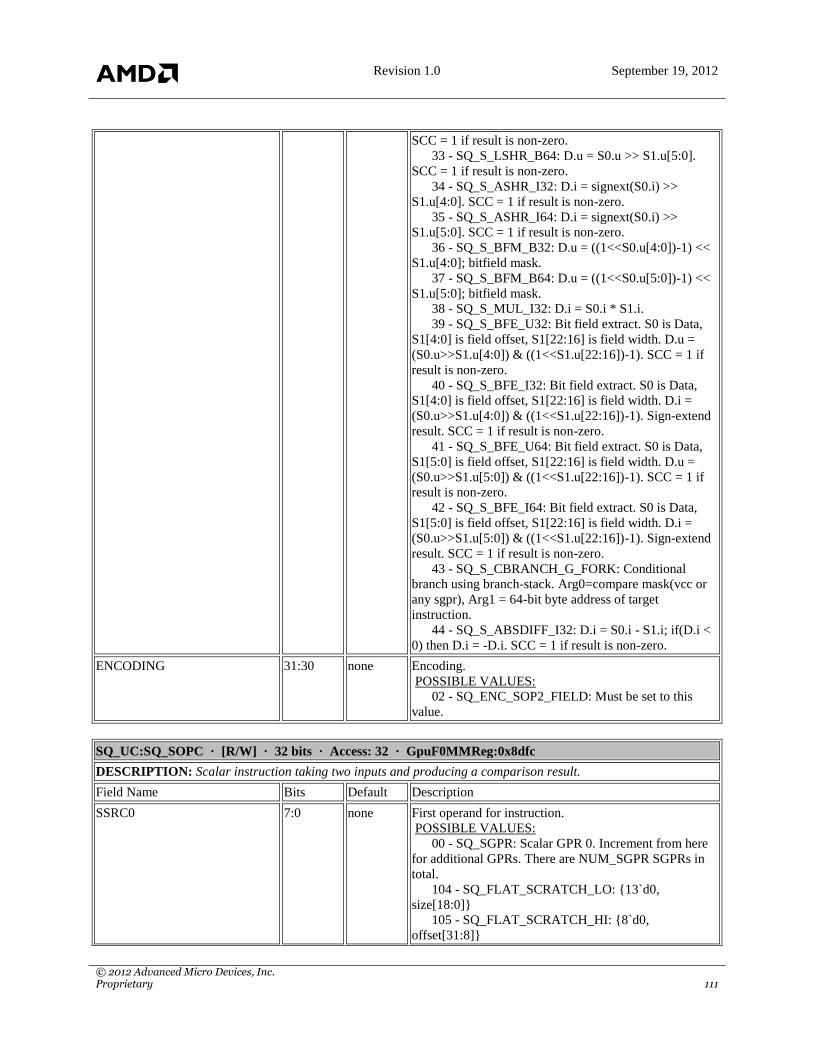
Revision 1.0 September 19, 2012
© 2012 Advanced Micro Devices, Inc. Proprietary 111
SCC = 1 if result is non-zero.
33 - SQ_S_LSHR_B64: D.u = S0.u >> S1.u[5:0].
SCC = 1 if result is non-zero.
34 - SQ_S_ASHR_I32: D.i = signext(S0.i) >>
S1.u[4:0]. SCC = 1 if result is non-zero.
35 - SQ_S_ASHR_I64: D.i = signext(S0.i) >>
S1.u[5:0]. SCC = 1 if result is non-zero.
36 - SQ_S_BFM_B32: D.u = ((1<<S0.u[4:0])-1) <<
S1.u[4:0]; bitfield mask.
37 - SQ_S_BFM_B64: D.u = ((1<<S0.u[5:0])-1) <<
S1.u[5:0]; bitfield mask.
38 - SQ_S_MUL_I32: D.i = S0.i * S1.i.
39 - SQ_S_BFE_U32: Bit field extract. S0 is Data,
S1[4:0] is field offset, S1[22:16] is field width. D.u =
(S0.u>>S1.u[4:0]) & ((1<<S1.u[22:16])-1). SCC = 1 if
result is non-zero.
40 - SQ_S_BFE_I32: Bit field extract. S0 is Data,
S1[4:0] is field offset, S1[22:16] is field width. D.i =
(S0.u>>S1.u[4:0]) & ((1<<S1.u[22:16])-1). Sign-extend
result. SCC = 1 if result is non-zero.
41 - SQ_S_BFE_U64: Bit field extract. S0 is Data,
S1[5:0] is field offset, S1[22:16] is field width. D.u =
(S0.u>>S1.u[5:0]) & ((1<<S1.u[22:16])-1). SCC = 1 if
result is non-zero.
42 - SQ_S_BFE_I64: Bit field extract. S0 is Data,
S1[5:0] is field offset, S1[22:16] is field width. D.i =
(S0.u>>S1.u[5:0]) & ((1<<S1.u[22:16])-1). Sign-extend
result. SCC = 1 if result is non-zero.
43 - SQ_S_CBRANCH_G_FORK: Conditional
branch using branch-stack. Arg0=compare mask(vcc or
any sgpr), Arg1 = 64-bit byte address of target
instruction.
44 - SQ_S_ABSDIFF_I32: D.i = S0.i - S1.i; if(D.i <
0) then D.i = -D.i. SCC = 1 if result is non-zero.
ENCODING 31:30 none Encoding.
POSSIBLE VALUES:
02 - SQ_ENC_SOP2_FIELD: Must be set to this
value.
SQ_UC:SQ_SOPC · [R/W] · 32 bits · Access: 32 · GpuF0MMReg:0x8dfc
DESCRIPTION: Scalar instruction taking two inputs and producing a comparison result.
Field Name Bits Default Description
SSRC0 7:0 none First operand for instruction.
POSSIBLE VALUES:
00 - SQ_SGPR: Scalar GPR 0. Increment from here
for additional GPRs. There are NUM_SGPR SGPRs in
total.
104 - SQ_FLAT_SCRATCH_LO: {13`d0,
size[18:0]}
105 - SQ_FLAT_SCRATCH_HI: {8`d0,
offset[31:8]}
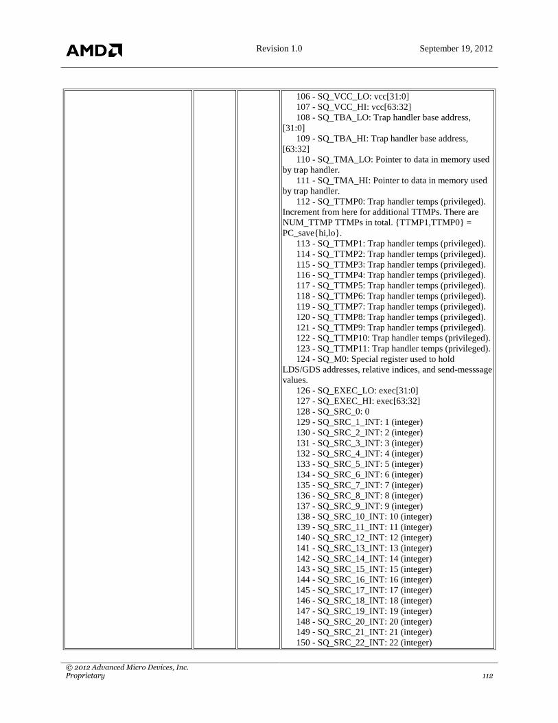
Revision 1.0 September 19, 2012
© 2012 Advanced Micro Devices, Inc. Proprietary 112
106 - SQ_VCC_LO: vcc[31:0]
107 - SQ_VCC_HI: vcc[63:32]
108 - SQ_TBA_LO: Trap handler base address,
[31:0]
109 - SQ_TBA_HI: Trap handler base address,
[63:32]
110 - SQ_TMA_LO: Pointer to data in memory used
by trap handler.
111 - SQ_TMA_HI: Pointer to data in memory used
by trap handler.
112 - SQ_TTMP0: Trap handler temps (privileged).
Increment from here for additional TTMPs. There are
NUM_TTMP TTMPs in total. {TTMP1,TTMP0} =
PC_save{hi,lo}.
113 - SQ_TTMP1: Trap handler temps (privileged).
114 - SQ_TTMP2: Trap handler temps (privileged).
115 - SQ_TTMP3: Trap handler temps (privileged).
116 - SQ_TTMP4: Trap handler temps (privileged).
117 - SQ_TTMP5: Trap handler temps (privileged).
118 - SQ_TTMP6: Trap handler temps (privileged).
119 - SQ_TTMP7: Trap handler temps (privileged).
120 - SQ_TTMP8: Trap handler temps (privileged).
121 - SQ_TTMP9: Trap handler temps (privileged).
122 - SQ_TTMP10: Trap handler temps (privileged).
123 - SQ_TTMP11: Trap handler temps (privileged).
124 - SQ_M0: Special register used to hold
LDS/GDS addresses, relative indices, and send-messsage
values.
126 - SQ_EXEC_LO: exec[31:0]
127 - SQ_EXEC_HI: exec[63:32]
128 - SQ_SRC_0: 0
129 - SQ_SRC_1_INT: 1 (integer)
130 - SQ_SRC_2_INT: 2 (integer)
131 - SQ_SRC_3_INT: 3 (integer)
132 - SQ_SRC_4_INT: 4 (integer)
133 - SQ_SRC_5_INT: 5 (integer)
134 - SQ_SRC_6_INT: 6 (integer)
135 - SQ_SRC_7_INT: 7 (integer)
136 - SQ_SRC_8_INT: 8 (integer)
137 - SQ_SRC_9_INT: 9 (integer)
138 - SQ_SRC_10_INT: 10 (integer)
139 - SQ_SRC_11_INT: 11 (integer)
140 - SQ_SRC_12_INT: 12 (integer)
141 - SQ_SRC_13_INT: 13 (integer)
142 - SQ_SRC_14_INT: 14 (integer)
143 - SQ_SRC_15_INT: 15 (integer)
144 - SQ_SRC_16_INT: 16 (integer)
145 - SQ_SRC_17_INT: 17 (integer)
146 - SQ_SRC_18_INT: 18 (integer)
147 - SQ_SRC_19_INT: 19 (integer)
148 - SQ_SRC_20_INT: 20 (integer)
149 - SQ_SRC_21_INT: 21 (integer)
150 - SQ_SRC_22_INT: 22 (integer)

Revision 1.0 September 19, 2012
© 2012 Advanced Micro Devices, Inc. Proprietary 113
151 - SQ_SRC_23_INT: 23 (integer)
152 - SQ_SRC_24_INT: 24 (integer)
153 - SQ_SRC_25_INT: 25 (integer)
154 - SQ_SRC_26_INT: 26 (integer)
155 - SQ_SRC_27_INT: 27 (integer)
156 - SQ_SRC_28_INT: 28 (integer)
157 - SQ_SRC_29_INT: 29 (integer)
158 - SQ_SRC_30_INT: 30 (integer)
159 - SQ_SRC_31_INT: 31 (integer)
160 - SQ_SRC_32_INT: 32 (integer)
161 - SQ_SRC_33_INT: 33 (integer)
162 - SQ_SRC_34_INT: 34 (integer)
163 - SQ_SRC_35_INT: 35 (integer)
164 - SQ_SRC_36_INT: 36 (integer)
165 - SQ_SRC_37_INT: 37 (integer)
166 - SQ_SRC_38_INT: 38 (integer)
167 - SQ_SRC_39_INT: 39 (integer)
168 - SQ_SRC_40_INT: 40 (integer)
169 - SQ_SRC_41_INT: 41 (integer)
170 - SQ_SRC_42_INT: 42 (integer)
171 - SQ_SRC_43_INT: 43 (integer)
172 - SQ_SRC_44_INT: 44 (integer)
173 - SQ_SRC_45_INT: 45 (integer)
174 - SQ_SRC_46_INT: 46 (integer)
175 - SQ_SRC_47_INT: 47 (integer)
176 - SQ_SRC_48_INT: 48 (integer)
177 - SQ_SRC_49_INT: 49 (integer)
178 - SQ_SRC_50_INT: 50 (integer)
179 - SQ_SRC_51_INT: 51 (integer)
180 - SQ_SRC_52_INT: 52 (integer)
181 - SQ_SRC_53_INT: 53 (integer)
182 - SQ_SRC_54_INT: 54 (integer)
183 - SQ_SRC_55_INT: 55 (integer)
184 - SQ_SRC_56_INT: 56 (integer)
185 - SQ_SRC_57_INT: 57 (integer)
186 - SQ_SRC_58_INT: 58 (integer)
187 - SQ_SRC_59_INT: 59 (integer)
188 - SQ_SRC_60_INT: 60 (integer)
189 - SQ_SRC_61_INT: 61 (integer)
190 - SQ_SRC_62_INT: 62 (integer)
191 - SQ_SRC_63_INT: 63 (integer)
192 - SQ_SRC_64_INT: 64 (integer)
193 - SQ_SRC_M_1_INT: -1 (integer)
194 - SQ_SRC_M_2_INT: -2 (integer)
195 - SQ_SRC_M_3_INT: -3 (integer)
196 - SQ_SRC_M_4_INT: -4 (integer)
197 - SQ_SRC_M_5_INT: -5 (integer)
198 - SQ_SRC_M_6_INT: -6 (integer)
199 - SQ_SRC_M_7_INT: -7 (integer)
200 - SQ_SRC_M_8_INT: -8 (integer)
201 - SQ_SRC_M_9_INT: -9 (integer)
202 - SQ_SRC_M_10_INT: -10 (integer)
203 - SQ_SRC_M_11_INT: -11 (integer)
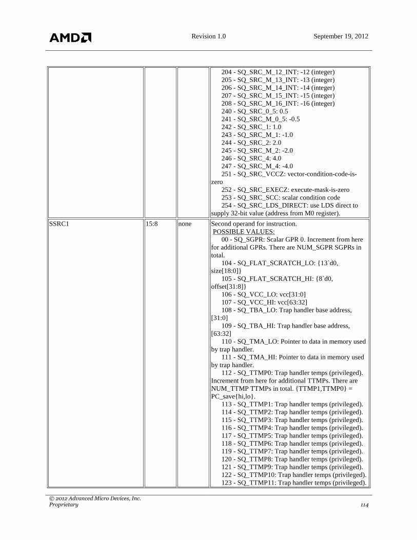
Revision 1.0 September 19, 2012
© 2012 Advanced Micro Devices, Inc. Proprietary 114
204 - SQ_SRC_M_12_INT: -12 (integer)
205 - SQ_SRC_M_13_INT: -13 (integer)
206 - SQ_SRC_M_14_INT: -14 (integer)
207 - SQ_SRC_M_15_INT: -15 (integer)
208 - SQ_SRC_M_16_INT: -16 (integer)
240 - SQ_SRC_0_5: 0.5
241 - SQ_SRC_M_0_5: -0.5
242 - SQ_SRC_1: 1.0
243 - SQ_SRC_M_1: -1.0
244 - SQ_SRC_2: 2.0
245 - SQ_SRC_M_2: -2.0
246 - SQ_SRC_4: 4.0
247 - SQ_SRC_M_4: -4.0
251 - SQ_SRC_VCCZ: vector-condition-code-is-
zero
252 - SQ_SRC_EXECZ: execute-mask-is-zero
253 - SQ_SRC_SCC: scalar condition code
254 - SQ_SRC_LDS_DIRECT: use LDS direct to
supply 32-bit value (address from M0 register).
SSRC1 15:8 none Second operand for instruction.
POSSIBLE VALUES:
00 - SQ_SGPR: Scalar GPR 0. Increment from here
for additional GPRs. There are NUM_SGPR SGPRs in
total.
104 - SQ_FLAT_SCRATCH_LO: {13`d0,
size[18:0]}
105 - SQ_FLAT_SCRATCH_HI: {8`d0,
offset[31:8]}
106 - SQ_VCC_LO: vcc[31:0]
107 - SQ_VCC_HI: vcc[63:32]
108 - SQ_TBA_LO: Trap handler base address,
[31:0]
109 - SQ_TBA_HI: Trap handler base address,
[63:32]
110 - SQ_TMA_LO: Pointer to data in memory used
by trap handler.
111 - SQ_TMA_HI: Pointer to data in memory used
by trap handler.
112 - SQ_TTMP0: Trap handler temps (privileged).
Increment from here for additional TTMPs. There are
NUM_TTMP TTMPs in total. {TTMP1,TTMP0} =
PC_save{hi,lo}.
113 - SQ_TTMP1: Trap handler temps (privileged).
114 - SQ_TTMP2: Trap handler temps (privileged).
115 - SQ_TTMP3: Trap handler temps (privileged).
116 - SQ_TTMP4: Trap handler temps (privileged).
117 - SQ_TTMP5: Trap handler temps (privileged).
118 - SQ_TTMP6: Trap handler temps (privileged).
119 - SQ_TTMP7: Trap handler temps (privileged).
120 - SQ_TTMP8: Trap handler temps (privileged).
121 - SQ_TTMP9: Trap handler temps (privileged).
122 - SQ_TTMP10: Trap handler temps (privileged).
123 - SQ_TTMP11: Trap handler temps (privileged).

Revision 1.0 September 19, 2012
© 2012 Advanced Micro Devices, Inc. Proprietary 115
124 - SQ_M0: Special register used to hold
LDS/GDS addresses, relative indices, and send-messsage
values.
126 - SQ_EXEC_LO: exec[31:0]
127 - SQ_EXEC_HI: exec[63:32]
128 - SQ_SRC_0: 0
129 - SQ_SRC_1_INT: 1 (integer)
130 - SQ_SRC_2_INT: 2 (integer)
131 - SQ_SRC_3_INT: 3 (integer)
132 - SQ_SRC_4_INT: 4 (integer)
133 - SQ_SRC_5_INT: 5 (integer)
134 - SQ_SRC_6_INT: 6 (integer)
135 - SQ_SRC_7_INT: 7 (integer)
136 - SQ_SRC_8_INT: 8 (integer)
137 - SQ_SRC_9_INT: 9 (integer)
138 - SQ_SRC_10_INT: 10 (integer)
139 - SQ_SRC_11_INT: 11 (integer)
140 - SQ_SRC_12_INT: 12 (integer)
141 - SQ_SRC_13_INT: 13 (integer)
142 - SQ_SRC_14_INT: 14 (integer)
143 - SQ_SRC_15_INT: 15 (integer)
144 - SQ_SRC_16_INT: 16 (integer)
145 - SQ_SRC_17_INT: 17 (integer)
146 - SQ_SRC_18_INT: 18 (integer)
147 - SQ_SRC_19_INT: 19 (integer)
148 - SQ_SRC_20_INT: 20 (integer)
149 - SQ_SRC_21_INT: 21 (integer)
150 - SQ_SRC_22_INT: 22 (integer)
151 - SQ_SRC_23_INT: 23 (integer)
152 - SQ_SRC_24_INT: 24 (integer)
153 - SQ_SRC_25_INT: 25 (integer)
154 - SQ_SRC_26_INT: 26 (integer)
155 - SQ_SRC_27_INT: 27 (integer)
156 - SQ_SRC_28_INT: 28 (integer)
157 - SQ_SRC_29_INT: 29 (integer)
158 - SQ_SRC_30_INT: 30 (integer)
159 - SQ_SRC_31_INT: 31 (integer)
160 - SQ_SRC_32_INT: 32 (integer)
161 - SQ_SRC_33_INT: 33 (integer)
162 - SQ_SRC_34_INT: 34 (integer)
163 - SQ_SRC_35_INT: 35 (integer)
164 - SQ_SRC_36_INT: 36 (integer)
165 - SQ_SRC_37_INT: 37 (integer)
166 - SQ_SRC_38_INT: 38 (integer)
167 - SQ_SRC_39_INT: 39 (integer)
168 - SQ_SRC_40_INT: 40 (integer)
169 - SQ_SRC_41_INT: 41 (integer)
170 - SQ_SRC_42_INT: 42 (integer)
171 - SQ_SRC_43_INT: 43 (integer)
172 - SQ_SRC_44_INT: 44 (integer)
173 - SQ_SRC_45_INT: 45 (integer)
174 - SQ_SRC_46_INT: 46 (integer)
175 - SQ_SRC_47_INT: 47 (integer)

Revision 1.0 September 19, 2012
© 2012 Advanced Micro Devices, Inc. Proprietary 116
176 - SQ_SRC_48_INT: 48 (integer)
177 - SQ_SRC_49_INT: 49 (integer)
178 - SQ_SRC_50_INT: 50 (integer)
179 - SQ_SRC_51_INT: 51 (integer)
180 - SQ_SRC_52_INT: 52 (integer)
181 - SQ_SRC_53_INT: 53 (integer)
182 - SQ_SRC_54_INT: 54 (integer)
183 - SQ_SRC_55_INT: 55 (integer)
184 - SQ_SRC_56_INT: 56 (integer)
185 - SQ_SRC_57_INT: 57 (integer)
186 - SQ_SRC_58_INT: 58 (integer)
187 - SQ_SRC_59_INT: 59 (integer)
188 - SQ_SRC_60_INT: 60 (integer)
189 - SQ_SRC_61_INT: 61 (integer)
190 - SQ_SRC_62_INT: 62 (integer)
191 - SQ_SRC_63_INT: 63 (integer)
192 - SQ_SRC_64_INT: 64 (integer)
193 - SQ_SRC_M_1_INT: -1 (integer)
194 - SQ_SRC_M_2_INT: -2 (integer)
195 - SQ_SRC_M_3_INT: -3 (integer)
196 - SQ_SRC_M_4_INT: -4 (integer)
197 - SQ_SRC_M_5_INT: -5 (integer)
198 - SQ_SRC_M_6_INT: -6 (integer)
199 - SQ_SRC_M_7_INT: -7 (integer)
200 - SQ_SRC_M_8_INT: -8 (integer)
201 - SQ_SRC_M_9_INT: -9 (integer)
202 - SQ_SRC_M_10_INT: -10 (integer)
203 - SQ_SRC_M_11_INT: -11 (integer)
204 - SQ_SRC_M_12_INT: -12 (integer)
205 - SQ_SRC_M_13_INT: -13 (integer)
206 - SQ_SRC_M_14_INT: -14 (integer)
207 - SQ_SRC_M_15_INT: -15 (integer)
208 - SQ_SRC_M_16_INT: -16 (integer)
240 - SQ_SRC_0_5: 0.5
241 - SQ_SRC_M_0_5: -0.5
242 - SQ_SRC_1: 1.0
243 - SQ_SRC_M_1: -1.0
244 - SQ_SRC_2: 2.0
245 - SQ_SRC_M_2: -2.0
246 - SQ_SRC_4: 4.0
247 - SQ_SRC_M_4: -4.0
251 - SQ_SRC_VCCZ: vector-condition-code-is-
zero
252 - SQ_SRC_EXECZ: execute-mask-is-zero
253 - SQ_SRC_SCC: scalar condition code
254 - SQ_SRC_LDS_DIRECT: use LDS direct to
supply 32-bit value (address from M0 register).
OP 22:16 none Opcode.
POSSIBLE VALUES:
00 - SQ_S_CMP_EQ_I32: SCC = (S0.i == S1.i).
01 - SQ_S_CMP_LG_I32: SCC = (S0.i != S1.i).
02 - SQ_S_CMP_GT_I32: SCC = (S0.i > S1.i).
03 - SQ_S_CMP_GE_I32: SCC = (S0.i >= S1.i).

Revision 1.0 September 19, 2012
© 2012 Advanced Micro Devices, Inc. Proprietary 117
04 - SQ_S_CMP_LT_I32: SCC = (S0.i < S1.i).
05 - SQ_S_CMP_LE_I32: SCC = (S0.i <= S1.i).
06 - SQ_S_CMP_EQ_U32: SCC = (S0.u == S1.u).
07 - SQ_S_CMP_LG_U32: SCC = (S0.u != S1.u).
08 - SQ_S_CMP_GT_U32: SCC = (S0.u > S1.u).
09 - SQ_S_CMP_GE_U32: SCC = (S0.u >= S1.u).
10 - SQ_S_CMP_LT_U32: SCC = (S0.u < S1.u).
11 - SQ_S_CMP_LE_U32: SCC = (S0.u <= S1.u).
12 - SQ_S_BITCMP0_B32: SCC = (S0.u[S1.u[4:0]]
== 0).
13 - SQ_S_BITCMP1_B32: SCC = (S0.u[S1.u[4:0]]
== 1).
14 - SQ_S_BITCMP0_B64: SCC = (S0.u[S1.u[5:0]]
== 0).
15 - SQ_S_BITCMP1_B64: SCC = (S0.u[S1.u[5:0]]
== 1).
16 - SQ_S_SETVSKIP: VSKIP = S0.u[S1.u[4:0]].
Enables and disables VSKIP mode. Requires one
waitstate after executing.
ENCODING 31:23 none Encoding.
POSSIBLE VALUES:
382 - SQ_ENC_SOPC_FIELD: Must be set to this
value.
SQ_UC:SQ_SOPK · [R/W] · 32 bits · Access: 32 · GpuF0MMReg:0x8dfc
DESCRIPTION: Scalar instruction taking one inline constant input and producing one output.
Field Name Bits Default Description
SIMM16 15:0 none 16-bit integer input for opcode. Signedness is determined
by opcode.
SDST 22:16 none Destination for instruction.
POSSIBLE VALUES:
00 - SQ_SGPR: Scalar GPR 0. Increment from here
for additional GPRs. There are NUM_SGPR SGPRs in
total.
104 - SQ_FLAT_SCRATCH_LO: {13`d0,
size[18:0]}
105 - SQ_FLAT_SCRATCH_HI: {8`d0,
offset[31:8]}
106 - SQ_VCC_LO: vcc[31:0]
107 - SQ_VCC_HI: vcc[63:32]
108 - SQ_TBA_LO: Trap handler base address,
[31:0]
109 - SQ_TBA_HI: Trap handler base address,
[63:32]
110 - SQ_TMA_LO: Pointer to data in memory used
by trap handler.
111 - SQ_TMA_HI: Pointer to data in memory used
by trap handler.
112 - SQ_TTMP0: Trap handler temps (privileged).
Increment from here for additional TTMPs. There are
NUM_TTMP TTMPs in total. {TTMP1,TTMP0} =
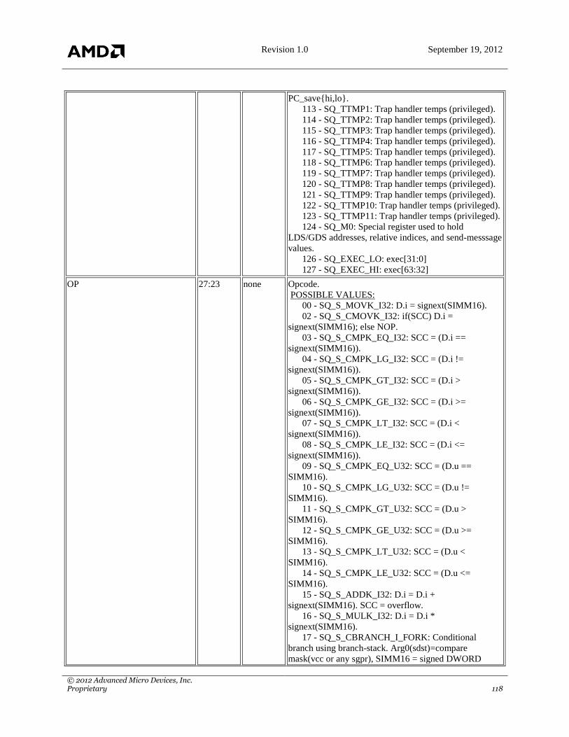
Revision 1.0 September 19, 2012
© 2012 Advanced Micro Devices, Inc. Proprietary 118
PC_save{hi,lo}.
113 - SQ_TTMP1: Trap handler temps (privileged).
114 - SQ_TTMP2: Trap handler temps (privileged).
115 - SQ_TTMP3: Trap handler temps (privileged).
116 - SQ_TTMP4: Trap handler temps (privileged).
117 - SQ_TTMP5: Trap handler temps (privileged).
118 - SQ_TTMP6: Trap handler temps (privileged).
119 - SQ_TTMP7: Trap handler temps (privileged).
120 - SQ_TTMP8: Trap handler temps (privileged).
121 - SQ_TTMP9: Trap handler temps (privileged).
122 - SQ_TTMP10: Trap handler temps (privileged).
123 - SQ_TTMP11: Trap handler temps (privileged).
124 - SQ_M0: Special register used to hold
LDS/GDS addresses, relative indices, and send-messsage
values.
126 - SQ_EXEC_LO: exec[31:0]
127 - SQ_EXEC_HI: exec[63:32]
OP 27:23 none Opcode.
POSSIBLE VALUES:
00 - SQ_S_MOVK_I32: D.i = signext(SIMM16).
02 - SQ_S_CMOVK_I32: if(SCC) D.i =
signext(SIMM16); else NOP.
03 - SQ_S_CMPK_EQ_I32: SCC = (D.i ==
signext(SIMM16)).
04 - SQ_S_CMPK_LG_I32: SCC = (D.i !=
signext(SIMM16)).
05 - SQ_S_CMPK_GT_I32: SCC = (D.i >
signext(SIMM16)).
06 - SQ_S_CMPK_GE_I32: SCC = (D.i >=
signext(SIMM16)).
07 - SQ_S_CMPK_LT_I32: SCC = (D.i <
signext(SIMM16)).
08 - SQ_S_CMPK_LE_I32: SCC = (D.i <=
signext(SIMM16)).
09 - SQ_S_CMPK_EQ_U32: SCC = (D.u ==
SIMM16).
10 - SQ_S_CMPK_LG_U32: SCC = (D.u !=
SIMM16).
11 - SQ_S_CMPK_GT_U32: SCC = (D.u >
SIMM16).
12 - SQ_S_CMPK_GE_U32: SCC = (D.u >=
SIMM16).
13 - SQ_S_CMPK_LT_U32: SCC = (D.u <
SIMM16).
14 - SQ_S_CMPK_LE_U32: SCC = (D.u <=
SIMM16).
15 - SQ_S_ADDK_I32: D.i = D.i +
signext(SIMM16). SCC = overflow.
16 - SQ_S_MULK_I32: D.i = D.i *
signext(SIMM16).
17 - SQ_S_CBRANCH_I_FORK: Conditional
branch using branch-stack. Arg0(sdst)=compare
mask(vcc or any sgpr), SIMM16 = signed DWORD
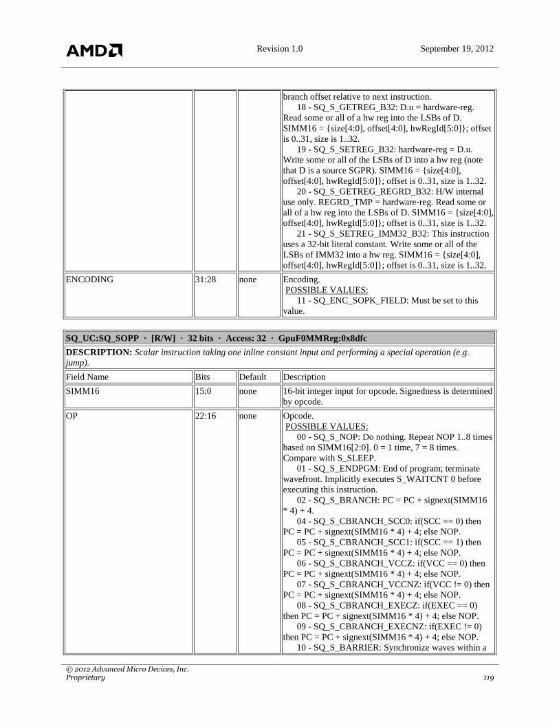
Revision 1.0 September 19, 2012
© 2012 Advanced Micro Devices, Inc. Proprietary 119
branch offset relative to next instruction.
18 - SQ_S_GETREG_B32: D.u = hardware-reg.
Read some or all of a hw reg into the LSBs of D.
SIMM16 = {size[4:0], offset[4:0], hwRegId[5:0]}; offset
is 0..31, size is 1..32.
19 - SQ_S_SETREG_B32: hardware-reg = D.u.
Write some or all of the LSBs of D into a hw reg (note
that D is a source SGPR). SIMM16 = {size[4:0],
offset[4:0], hwRegId[5:0]}; offset is 0..31, size is 1..32.
20 - SQ_S_GETREG_REGRD_B32: H/W internal
use only. REGRD_TMP = hardware-reg. Read some or
all of a hw reg into the LSBs of D. SIMM16 = {size[4:0],
offset[4:0], hwRegId[5:0]}; offset is 0..31, size is 1..32.
21 - SQ_S_SETREG_IMM32_B32: This instruction
uses a 32-bit literal constant. Write some or all of the
LSBs of IMM32 into a hw reg. SIMM16 = {size[4:0],
offset[4:0], hwRegId[5:0]}; offset is 0..31, size is 1..32.
ENCODING 31:28 none Encoding.
POSSIBLE VALUES:
11 - SQ_ENC_SOPK_FIELD: Must be set to this
value.
SQ_UC:SQ_SOPP · [R/W] · 32 bits · Access: 32 · GpuF0MMReg:0x8dfc
DESCRIPTION: Scalar instruction taking one inline constant input and performing a special operation (e.g.
jump).
Field Name Bits Default Description
SIMM16 15:0 none 16-bit integer input for opcode. Signedness is determined
by opcode.
OP 22:16 none Opcode.
POSSIBLE VALUES:
00 - SQ_S_NOP: Do nothing. Repeat NOP 1..8 times
based on SIMM16[2:0]. 0 = 1 time, 7 = 8 times.
Compare with S_SLEEP.
01 - SQ_S_ENDPGM: End of program; terminate
wavefront. Implicitly executes S_WAITCNT 0 before
executing this instruction.
02 - SQ_S_BRANCH: PC = PC + signext(SIMM16
* 4) + 4.
04 - SQ_S_CBRANCH_SCC0: if(SCC == 0) then
PC = PC + signext(SIMM16 * 4) + 4; else NOP.
05 - SQ_S_CBRANCH_SCC1: if(SCC == 1) then
PC = PC + signext(SIMM16 * 4) + 4; else NOP.
06 - SQ_S_CBRANCH_VCCZ: if(VCC == 0) then
PC = PC + signext(SIMM16 * 4) + 4; else NOP.
07 - SQ_S_CBRANCH_VCCNZ: if(VCC != 0) then
PC = PC + signext(SIMM16 * 4) + 4; else NOP.
08 - SQ_S_CBRANCH_EXECZ: if(EXEC == 0)
then PC = PC + signext(SIMM16 * 4) + 4; else NOP.
09 - SQ_S_CBRANCH_EXECNZ: if(EXEC != 0)
then PC = PC + signext(SIMM16 * 4) + 4; else NOP.
10 - SQ_S_BARRIER: Synchronize waves within a

Revision 1.0 September 19, 2012
© 2012 Advanced Micro Devices, Inc. Proprietary 120
threadgroup. If not all waves of the threadgroup have
been created yet, waits for entire group before
proceeding.
11 - SQ_S_SETKILL: set KILL bit to value of
SIMM16[0]. Used primarily for debugging kill wave
cmd behavior.
12 - SQ_S_WAITCNT: Wait for count of
outstanding lds, vector-memory and export/vmem-write-
data to be at or below the specified levels. SIMM16[3:0]
= vmcount, SIMM16[6:4] = export/mem-write-data
count, SIMM16[12:8] = LGKM_cnt (scalar-
mem/GDS/LDS count).
13 - SQ_S_SETHALT: set HALT bit to value of
SIMM16[0]. 1 = halt, 0 = resume. The halt flag is
ignored while PRIV == 1.
14 - SQ_S_SLEEP: Cause a wave to sleep for (64 *
SIMM16[2:0] + 1..64) clocks; the exact amount of delay
is approximate. Compare with S_NOP.
15 - SQ_S_SETPRIO: User settable wave priority is
set to SIMM16[1:0]. 0 = lowest, 3 = highest. The overall
wave priority is {SPIPrio[1:0] + UserPrio[1:0],
WaveAge[3:0]}.
16 - SQ_S_SENDMSG: Send a message upstream to
VGT or the interrupt handler. SIMM16[9:0] contains the
message type and is documented in the shader
programming guide.
17 - SQ_S_SENDMSGHALT: Send a message and
then HALT the wavefront; see S_SENDMSG for details.
18 - SQ_S_TRAP: Enter the trap handler. TrapID =
SIMM16[7:0]. Wait for all instructions to complete; set
{TTMP1, TTMP0} = {3`h0, PCRewind[3:0], HT[0],
TrapID[7:0], PC[47:0]}; into {TTMP0,TTMP1}; PC =
TBA (trap base address); PRIV = 1. This instruction may
be generated internally as well in response to a host trap
(HT = 1) or an exception. TrapID 0 is reserved for
hardware use.
19 - SQ_S_ICACHE_INV: Invalidate entire L1
instruction cache. You must have 12 NOPs or a
jump/branch instruction after this instruction to ensure
the SQ instruction buffer gets purged.
20 - SQ_S_INCPERFLEVEL: Increment
performance counter specified in SIMM16[3:0] by 1.
21 - SQ_S_DECPERFLEVEL: Decrement
performance counter specified in SIMM16[3:0] by 1.
22 - SQ_S_TTRACEDATA: Send M0 as user data to
the thread trace stream.
23 - SQ_S_CBRANCH_CDBGSYS:
if(conditional_debug_system != 0) then PC = PC +
signext(SIMM16 * 4) + 4; else NOP.
24 - SQ_S_CBRANCH_CDBGUSER:
if(conditional_debug_user != 0) then PC = PC +
signext(SIMM16 * 4) + 4; else NOP.
25 - SQ_S_CBRANCH_CDBGSYS_OR_USER:

Revision 1.0 September 19, 2012
© 2012 Advanced Micro Devices, Inc. Proprietary 121
if(conditional_debug_system || conditional_debug_user)
then PC = PC + signext(SIMM16 * 4) + 4; else NOP.
26 - SQ_S_CBRANCH_CDBGSYS_AND_USER:
if(conditional_debug_system &&
conditional_debug_user) then PC = PC +
signext(SIMM16 * 4) + 4; else NOP.
ENCODING 31:23 none Encoding.
POSSIBLE VALUES:
383 - SQ_ENC_SOPP_FIELD: Must be set to this
value.
SQ_UC:SQ_VINTRP · [R/W] · 32 bits · Access: 32 · GpuF0MMReg:0x8dfc
DESCRIPTION: Interpolate data for the pixel shader.
Field Name Bits Default Description
VSRC 7:0 none VGPR containing the i/j coordinate to multiply one of
the parameter components by.
POSSIBLE VALUES:
00 - SQ_VGPR: Vector GPR 0. Increment from here
for additional GPRs. There are NUM_VGPR VGPRs in
total.
ATTRCHAN 9:8 none Attribute component to interpolate.
POSSIBLE VALUES:
00 - SQ_CHAN_X: Process X channel
01 - SQ_CHAN_Y: Process Y channel
02 - SQ_CHAN_Z: Process Z channel
03 - SQ_CHAN_W: Process W channel
ATTR 15:10 none Attribute to interpolate.
POSSIBLE VALUES:
00 - SQ_ATTR: First interpolation attribute.
Increment from here for additional attributes. There are
SQ_NUM_ATTR attributes in total.
OP 17:16 none Opcode.
POSSIBLE VALUES:
00 - SQ_V_INTERP_P1_F32: D.f = P10 * S.f + P0;
parameter interpolation (SQ translates to V_MAD_F32
for SP). CAUTION: when in HALF_LDS mode, D must
not be the same GPR as S; if D == S then data corruption
will occur.
01 - SQ_V_INTERP_P2_F32: D.f = P20 * S.f + D.f;
parameter interpolation (SQ translates to V_MAD_F32
for SP).
02 - SQ_V_INTERP_MOV_F32: D.f =
{P10,P20,P0}[S.u]; parameter load.
VDST 25:18 none VGPR to write results to, and optionally to read from
when accumulating results.
POSSIBLE VALUES:
00 - SQ_VGPR: Vector GPR 0. Increment from here
for additional GPRs. There are NUM_VGPR VGPRs in
total.

Revision 1.0 September 19, 2012
© 2012 Advanced Micro Devices, Inc. Proprietary 122
ENCODING 31:26 none Encoding.
POSSIBLE VALUES:
50 - SQ_ENC_VINTRP_FIELD: Must be set to this
value.
SQ_UC:SQ_VOP1 · [R/W] · 32 bits · Access: 32 · GpuF0MMReg:0x8dfc
DESCRIPTION: Vector instruction taking one input and producing one output.
Field Name Bits Default Description
SRC0 8:0 none First operand for instruction.
POSSIBLE VALUES:
00 - SQ_SGPR: Scalar GPR 0. Increment from here
for additional GPRs. There are NUM_SGPR SGPRs in
total.
104 - SQ_FLAT_SCRATCH_LO: {13`d0,
size[18:0]}
105 - SQ_FLAT_SCRATCH_HI: {8`d0,
offset[31:8]}
106 - SQ_VCC_LO: vcc[31:0]
107 - SQ_VCC_HI: vcc[63:32]
108 - SQ_TBA_LO: Trap handler base address,
[31:0]
109 - SQ_TBA_HI: Trap handler base address,
[63:32]
110 - SQ_TMA_LO: Pointer to data in memory used
by trap handler.
111 - SQ_TMA_HI: Pointer to data in memory used
by trap handler.
112 - SQ_TTMP0: Trap handler temps (privileged).
Increment from here for additional TTMPs. There are
NUM_TTMP TTMPs in total. {TTMP1,TTMP0} =
PC_save{hi,lo}.
113 - SQ_TTMP1: Trap handler temps (privileged).
114 - SQ_TTMP2: Trap handler temps (privileged).
115 - SQ_TTMP3: Trap handler temps (privileged).
116 - SQ_TTMP4: Trap handler temps (privileged).
117 - SQ_TTMP5: Trap handler temps (privileged).
118 - SQ_TTMP6: Trap handler temps (privileged).
119 - SQ_TTMP7: Trap handler temps (privileged).
120 - SQ_TTMP8: Trap handler temps (privileged).
121 - SQ_TTMP9: Trap handler temps (privileged).
122 - SQ_TTMP10: Trap handler temps (privileged).
123 - SQ_TTMP11: Trap handler temps (privileged).
124 - SQ_M0: Special register used to hold
LDS/GDS addresses, relative indices, and send-messsage
values.
126 - SQ_EXEC_LO: exec[31:0]
127 - SQ_EXEC_HI: exec[63:32]
128 - SQ_SRC_0: 0
129 - SQ_SRC_1_INT: 1 (integer)
130 - SQ_SRC_2_INT: 2 (integer)
131 - SQ_SRC_3_INT: 3 (integer)
132 - SQ_SRC_4_INT: 4 (integer)

Revision 1.0 September 19, 2012
© 2012 Advanced Micro Devices, Inc. Proprietary 123
133 - SQ_SRC_5_INT: 5 (integer)
134 - SQ_SRC_6_INT: 6 (integer)
135 - SQ_SRC_7_INT: 7 (integer)
136 - SQ_SRC_8_INT: 8 (integer)
137 - SQ_SRC_9_INT: 9 (integer)
138 - SQ_SRC_10_INT: 10 (integer)
139 - SQ_SRC_11_INT: 11 (integer)
140 - SQ_SRC_12_INT: 12 (integer)
141 - SQ_SRC_13_INT: 13 (integer)
142 - SQ_SRC_14_INT: 14 (integer)
143 - SQ_SRC_15_INT: 15 (integer)
144 - SQ_SRC_16_INT: 16 (integer)
145 - SQ_SRC_17_INT: 17 (integer)
146 - SQ_SRC_18_INT: 18 (integer)
147 - SQ_SRC_19_INT: 19 (integer)
148 - SQ_SRC_20_INT: 20 (integer)
149 - SQ_SRC_21_INT: 21 (integer)
150 - SQ_SRC_22_INT: 22 (integer)
151 - SQ_SRC_23_INT: 23 (integer)
152 - SQ_SRC_24_INT: 24 (integer)
153 - SQ_SRC_25_INT: 25 (integer)
154 - SQ_SRC_26_INT: 26 (integer)
155 - SQ_SRC_27_INT: 27 (integer)
156 - SQ_SRC_28_INT: 28 (integer)
157 - SQ_SRC_29_INT: 29 (integer)
158 - SQ_SRC_30_INT: 30 (integer)
159 - SQ_SRC_31_INT: 31 (integer)
160 - SQ_SRC_32_INT: 32 (integer)
161 - SQ_SRC_33_INT: 33 (integer)
162 - SQ_SRC_34_INT: 34 (integer)
163 - SQ_SRC_35_INT: 35 (integer)
164 - SQ_SRC_36_INT: 36 (integer)
165 - SQ_SRC_37_INT: 37 (integer)
166 - SQ_SRC_38_INT: 38 (integer)
167 - SQ_SRC_39_INT: 39 (integer)
168 - SQ_SRC_40_INT: 40 (integer)
169 - SQ_SRC_41_INT: 41 (integer)
170 - SQ_SRC_42_INT: 42 (integer)
171 - SQ_SRC_43_INT: 43 (integer)
172 - SQ_SRC_44_INT: 44 (integer)
173 - SQ_SRC_45_INT: 45 (integer)
174 - SQ_SRC_46_INT: 46 (integer)
175 - SQ_SRC_47_INT: 47 (integer)
176 - SQ_SRC_48_INT: 48 (integer)
177 - SQ_SRC_49_INT: 49 (integer)
178 - SQ_SRC_50_INT: 50 (integer)
179 - SQ_SRC_51_INT: 51 (integer)
180 - SQ_SRC_52_INT: 52 (integer)
181 - SQ_SRC_53_INT: 53 (integer)
182 - SQ_SRC_54_INT: 54 (integer)
183 - SQ_SRC_55_INT: 55 (integer)
184 - SQ_SRC_56_INT: 56 (integer)
185 - SQ_SRC_57_INT: 57 (integer)

Revision 1.0 September 19, 2012
© 2012 Advanced Micro Devices, Inc. Proprietary 124
186 - SQ_SRC_58_INT: 58 (integer)
187 - SQ_SRC_59_INT: 59 (integer)
188 - SQ_SRC_60_INT: 60 (integer)
189 - SQ_SRC_61_INT: 61 (integer)
190 - SQ_SRC_62_INT: 62 (integer)
191 - SQ_SRC_63_INT: 63 (integer)
192 - SQ_SRC_64_INT: 64 (integer)
193 - SQ_SRC_M_1_INT: -1 (integer)
194 - SQ_SRC_M_2_INT: -2 (integer)
195 - SQ_SRC_M_3_INT: -3 (integer)
196 - SQ_SRC_M_4_INT: -4 (integer)
197 - SQ_SRC_M_5_INT: -5 (integer)
198 - SQ_SRC_M_6_INT: -6 (integer)
199 - SQ_SRC_M_7_INT: -7 (integer)
200 - SQ_SRC_M_8_INT: -8 (integer)
201 - SQ_SRC_M_9_INT: -9 (integer)
202 - SQ_SRC_M_10_INT: -10 (integer)
203 - SQ_SRC_M_11_INT: -11 (integer)
204 - SQ_SRC_M_12_INT: -12 (integer)
205 - SQ_SRC_M_13_INT: -13 (integer)
206 - SQ_SRC_M_14_INT: -14 (integer)
207 - SQ_SRC_M_15_INT: -15 (integer)
208 - SQ_SRC_M_16_INT: -16 (integer)
240 - SQ_SRC_0_5: 0.5
241 - SQ_SRC_M_0_5: -0.5
242 - SQ_SRC_1: 1.0
243 - SQ_SRC_M_1: -1.0
244 - SQ_SRC_2: 2.0
245 - SQ_SRC_M_2: -2.0
246 - SQ_SRC_4: 4.0
247 - SQ_SRC_M_4: -4.0
251 - SQ_SRC_VCCZ: vector-condition-code-is-
zero
252 - SQ_SRC_EXECZ: execute-mask-is-zero
253 - SQ_SRC_SCC: scalar condition code
254 - SQ_SRC_LDS_DIRECT: use LDS direct to
supply 32-bit value (address from M0 register).
256 - SQ_SRC_VGPR: Vector GPR 0. Increment
from here for additional GPRs. There are NUM_VGPR
VGPRs in total. You may use the constant
SQ_SRC_VGPR_BIT to set or clear the high order bit
for vector GPRs in this operand.
OP 16:9 none Opcode.
POSSIBLE VALUES:
00 - SQ_V_NOP: Do nothing.
01 - SQ_V_MOV_B32: D.u = S0.u.
02 - SQ_V_READFIRSTLANE_B32: Copy one
VGPR value to one SGPR. Dst = SGPR destination, Src0
= source data (VGPR# or M0 for lds direct access),
Lane# = FindFirst1fromLSB(exec) (Lane# = 0 if exec is
zero). Ignores exec mask for the access. SQ translates to
V_READLANE_B32.
03 - SQ_V_CVT_I32_F64: D.i = (int)S0.d.

Revision 1.0 September 19, 2012
© 2012 Advanced Micro Devices, Inc. Proprietary 125
04 - SQ_V_CVT_F64_I32: D.d = (double)S0.i.
05 - SQ_V_CVT_F32_I32: D.f = (float)S0.i.
06 - SQ_V_CVT_F32_U32: D.f = (float)S0.u.
07 - SQ_V_CVT_U32_F32: D.u = (unsigned)S0.f.
08 - SQ_V_CVT_I32_F32: D.i = (int)S0.f.
09 - SQ_V_MOV_FED_B32: D.u = S0.u, introduce
EDC double error upon write to dest vgpr without
causing an exception.
10 - SQ_V_CVT_F16_F32: D.f16 =
flt32_to_flt16(S0.f).
11 - SQ_V_CVT_F32_F16: D.f =
flt16_to_flt32(S0.f16).
12 - SQ_V_CVT_RPI_I32_F32: D.i = (int)floor(S0.f
+ 0.5).
13 - SQ_V_CVT_FLR_I32_F32: D.i =
(int)floor(S0.f).
14 - SQ_V_CVT_OFF_F32_I4: 4-bit signed int to
32-bit float. For interpolation in shader.
15 - SQ_V_CVT_F32_F64: D.f = (float)S0.d.
16 - SQ_V_CVT_F64_F32: D.d = (double)S0.f.
17 - SQ_V_CVT_F32_UBYTE0: D.f =
UINT2FLT(S0.u[7:0]).
18 - SQ_V_CVT_F32_UBYTE1: D.f =
UINT2FLT(S0.u[15:8]).
19 - SQ_V_CVT_F32_UBYTE2: D.f =
UINT2FLT(S0.u[23:16]).
20 - SQ_V_CVT_F32_UBYTE3: D.f =
UINT2FLT(S0.u[31:24]).
21 - SQ_V_CVT_U32_F64: D.u = (unsigned)S0.d.
22 - SQ_V_CVT_F64_U32: D.d = (double)S0.u.
23 - SQ_V_TRUNC_F64: D.d = trunc(S0.d), return
integer part of S0.d.
24 - SQ_V_CEIL_F64: D.d = trunc(S0.d); if (S0.d >
0.0 && S0.d != D.d), D.d += 1.0.
25 - SQ_V_RNDNE_F64: D.d =
round_nearest_even(S0.d).
26 - SQ_V_FLOOR_F64: D.d = trunc(S0.d); if (S0.d
< 0.0 && S0.d != D.d), D.d += -1.0.
32 - SQ_V_FRACT_F32: D.f = S0.f - floor(S0.f).
33 - SQ_V_TRUNC_F32: D.f = trunc(S0.f), return
integer part of S0.f.
34 - SQ_V_CEIL_F32: D.f = trunc(S0.f); if (S0.f >
0.0 && S0.f != D.f), D.f += 1.0.
35 - SQ_V_RNDNE_F32: D.f =
round_nearest_even(S0.f).
36 - SQ_V_FLOOR_F32: D.f = trunc(S0.f); if (S0.f
< 0.0 && S0.f != D.f), D.f += -1.0.
37 - SQ_V_EXP_F32: D.f = pow(2.0, S0.f).
38 - SQ_V_LOG_CLAMP_F32: D.f = log2(S0.f).
Base 2 logarithm, result clamped to -MAX_FLOAT.
39 - SQ_V_LOG_F32: D.f = log2(S0.f). Base 2
logarithm.
40 - SQ_V_RCP_CLAMP_F32: D.f = 1.0 / S0.f.

Revision 1.0 September 19, 2012
© 2012 Advanced Micro Devices, Inc. Proprietary 126
Reciprocal, result clamped to +-MAX_FLOAT.
41 - SQ_V_RCP_LEGACY_F32: D.f = 1.0 / S0.f.
Reciprocal, result of +-INF clamped to +-0.0.
42 - SQ_V_RCP_F32: D.f = 1.0 / S0.f. Reciprocal
with IEEE rules and < 1ulp error.
43 - SQ_V_RCP_IFLAG_F32: D.f = 1.0 / S0.f.
Reciprocal intended for integer division, can raise integer
DIV_BY_ZERO exception but cannot raise floating-
point exceptions.
44 - SQ_V_RSQ_CLAMP_F32: D.f = 1.0 /
sqrt(S0.f). Reciprocal square root, result clamped to +-
MAX_FLOAT.
45 - SQ_V_RSQ_LEGACY_F32: D.f = 1.0 /
sqrt(S0.f). Reciprocal square root, if S0.f is +-0.0 then
the result is +0.0.
46 - SQ_V_RSQ_F32: D.f = 1.0 / sqrt(S0.f).
Reciprocal square root with IEEE rules.
47 - SQ_V_RCP_F64: D.d = 1.0 / S0.d.
48 - SQ_V_RCP_CLAMP_F64: D.d = 1.0 / (S0.d).
See V_RCP_CLAMP_F32.
49 - SQ_V_RSQ_F64: D.d = 1.0 / sqrt(S0.d). See
V_RSQ_F32.
50 - SQ_V_RSQ_CLAMP_F64: D.d = 1.0 /
sqrt(S0.d). See V_RSQ_CLAMP_F32.
51 - SQ_V_SQRT_F32: D.f = sqrt(S0.f).
52 - SQ_V_SQRT_F64: D.d = sqrt(S0.d).
53 - SQ_V_SIN_F32: D.f = sin(S0.f * 2 * PI). Valid
range of S0.f is [-256.0, +256.0]. Out of range input
results in float 0.0.
54 - SQ_V_COS_F32: D.f = cos(S0.f * 2 * PI). Valid
range of S0.f is [-256.0, +256.0]. Out of range input
results in float 1.0.
55 - SQ_V_NOT_B32: D.u = ~S0.u.
56 - SQ_V_BFREV_B32: D.u[31:0] = S0.u[0:31],
bitfield reverse.
57 - SQ_V_FFBH_U32: D.u = position of first 1 in
S0.u from MSB; D.u = 0xffffffff if S0.u == 0.
58 - SQ_V_FFBL_B32: D.u = position of first 1 in
S0.u from LSB; D.u = 0xffffffff if S0.u == 0.
59 - SQ_V_FFBH_I32: D.u = position of first bit
different from sign bit in S0.i from MSB; D.u = 0xffffffff
if S0.i == 0 or S0.i == 0xffffffff.
60 - SQ_V_FREXP_EXP_I32_F64: See
V_FREXP_EXP_I32_F32.
61 - SQ_V_FREXP_MANT_F64: See
V_FREXP_MANT_F32.
62 - SQ_V_FRACT_F64: See V_FRACT_F32.
63 - SQ_V_FREXP_EXP_I32_F32: if(S0.f == INF ||
S0.f == NAN) then D.i = 0; else D.i =
TwosComplement(Exponent(S0.f) - 127 + 1). Returns
exponent of single precision float input, such that S0.f =
significand * (2 ** exponent). See also
FREXP_MANT_F32, which returns the significand.

Revision 1.0 September 19, 2012
© 2012 Advanced Micro Devices, Inc. Proprietary 127
64 - SQ_V_FREXP_MANT_F32: if(S0.f == INF ||
S0.f == NAN) then D.f = S0.f; else D.f = Mantissa(S0.f).
Result range is in (-1.0,-0.5][0.5,1.0) in normal cases.
Returns binary significand of single precision float input,
such that S0.f = significand * (2 ** exponent). See also
FREXP_EXP_I32_F32, which returns integer exponent.
65 - SQ_V_CLREXCP: Clear wave`s exception state
in SIMD (SP).
66 - SQ_V_MOVRELD_B32: VGPR[D.u + M0.u] =
VGPR[S0.u]. SQ translates to V_MOV_B32.
67 - SQ_V_MOVRELS_B32: VGPR[D.u] =
VGPR[S0.u + M0.u]. SQ translates to V_MOV_B32.
68 - SQ_V_MOVRELSD_B32: VGPR[D.u + M0.u]
= VGPR[S0.u + M0.u]. SQ translates to V_MOV_B32.
69 - SQ_V_LOG_LEGACY_F32: D.f = log2(S0.f).
Base 2 logarithm, same as SI
70 - SQ_V_EXP_LEGACY_F32: D.f = pow(2.0,
S0.f). same as SI
VDST 24:17 none Destination for instruction.
POSSIBLE VALUES:
00 - SQ_VGPR: Vector GPR 0. Increment from here
for additional GPRs. There are NUM_VGPR VGPRs in
total.
ENCODING 31:25 none Encoding.
POSSIBLE VALUES:
63 - SQ_ENC_VOP1_FIELD: Must be set to this
value.
SQ_UC:SQ_VOP2 · [R/W] · 32 bits · Access: 32 · GpuF0MMReg:0x8dfc
DESCRIPTION: Vector instruction taking two inputs and producing one output.
Field Name Bits Default Description
SRC0 8:0 none First operand for instruction.
POSSIBLE VALUES:
00 - SQ_SGPR: Scalar GPR 0. Increment from here
for additional GPRs. There are NUM_SGPR SGPRs in
total.
104 - SQ_FLAT_SCRATCH_LO: {13`d0,
size[18:0]}
105 - SQ_FLAT_SCRATCH_HI: {8`d0,
offset[31:8]}
106 - SQ_VCC_LO: vcc[31:0]
107 - SQ_VCC_HI: vcc[63:32]
108 - SQ_TBA_LO: Trap handler base address,
[31:0]
109 - SQ_TBA_HI: Trap handler base address,
[63:32]
110 - SQ_TMA_LO: Pointer to data in memory used
by trap handler.
111 - SQ_TMA_HI: Pointer to data in memory used
by trap handler.
112 - SQ_TTMP0: Trap handler temps (privileged).
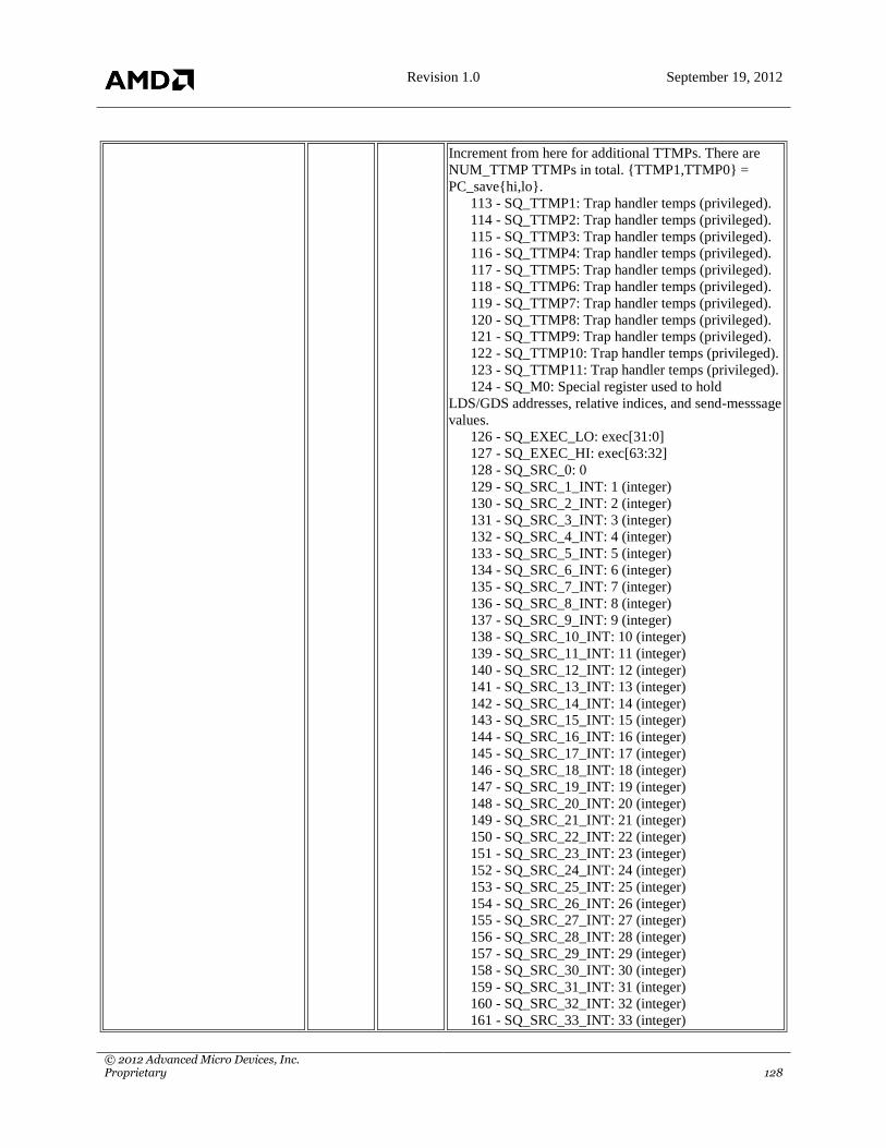
Revision 1.0 September 19, 2012
© 2012 Advanced Micro Devices, Inc. Proprietary 128
Increment from here for additional TTMPs. There are
NUM_TTMP TTMPs in total. {TTMP1,TTMP0} =
PC_save{hi,lo}.
113 - SQ_TTMP1: Trap handler temps (privileged).
114 - SQ_TTMP2: Trap handler temps (privileged).
115 - SQ_TTMP3: Trap handler temps (privileged).
116 - SQ_TTMP4: Trap handler temps (privileged).
117 - SQ_TTMP5: Trap handler temps (privileged).
118 - SQ_TTMP6: Trap handler temps (privileged).
119 - SQ_TTMP7: Trap handler temps (privileged).
120 - SQ_TTMP8: Trap handler temps (privileged).
121 - SQ_TTMP9: Trap handler temps (privileged).
122 - SQ_TTMP10: Trap handler temps (privileged).
123 - SQ_TTMP11: Trap handler temps (privileged).
124 - SQ_M0: Special register used to hold
LDS/GDS addresses, relative indices, and send-messsage
values.
126 - SQ_EXEC_LO: exec[31:0]
127 - SQ_EXEC_HI: exec[63:32]
128 - SQ_SRC_0: 0
129 - SQ_SRC_1_INT: 1 (integer)
130 - SQ_SRC_2_INT: 2 (integer)
131 - SQ_SRC_3_INT: 3 (integer)
132 - SQ_SRC_4_INT: 4 (integer)
133 - SQ_SRC_5_INT: 5 (integer)
134 - SQ_SRC_6_INT: 6 (integer)
135 - SQ_SRC_7_INT: 7 (integer)
136 - SQ_SRC_8_INT: 8 (integer)
137 - SQ_SRC_9_INT: 9 (integer)
138 - SQ_SRC_10_INT: 10 (integer)
139 - SQ_SRC_11_INT: 11 (integer)
140 - SQ_SRC_12_INT: 12 (integer)
141 - SQ_SRC_13_INT: 13 (integer)
142 - SQ_SRC_14_INT: 14 (integer)
143 - SQ_SRC_15_INT: 15 (integer)
144 - SQ_SRC_16_INT: 16 (integer)
145 - SQ_SRC_17_INT: 17 (integer)
146 - SQ_SRC_18_INT: 18 (integer)
147 - SQ_SRC_19_INT: 19 (integer)
148 - SQ_SRC_20_INT: 20 (integer)
149 - SQ_SRC_21_INT: 21 (integer)
150 - SQ_SRC_22_INT: 22 (integer)
151 - SQ_SRC_23_INT: 23 (integer)
152 - SQ_SRC_24_INT: 24 (integer)
153 - SQ_SRC_25_INT: 25 (integer)
154 - SQ_SRC_26_INT: 26 (integer)
155 - SQ_SRC_27_INT: 27 (integer)
156 - SQ_SRC_28_INT: 28 (integer)
157 - SQ_SRC_29_INT: 29 (integer)
158 - SQ_SRC_30_INT: 30 (integer)
159 - SQ_SRC_31_INT: 31 (integer)
160 - SQ_SRC_32_INT: 32 (integer)
161 - SQ_SRC_33_INT: 33 (integer)

Revision 1.0 September 19, 2012
© 2012 Advanced Micro Devices, Inc. Proprietary 129
162 - SQ_SRC_34_INT: 34 (integer)
163 - SQ_SRC_35_INT: 35 (integer)
164 - SQ_SRC_36_INT: 36 (integer)
165 - SQ_SRC_37_INT: 37 (integer)
166 - SQ_SRC_38_INT: 38 (integer)
167 - SQ_SRC_39_INT: 39 (integer)
168 - SQ_SRC_40_INT: 40 (integer)
169 - SQ_SRC_41_INT: 41 (integer)
170 - SQ_SRC_42_INT: 42 (integer)
171 - SQ_SRC_43_INT: 43 (integer)
172 - SQ_SRC_44_INT: 44 (integer)
173 - SQ_SRC_45_INT: 45 (integer)
174 - SQ_SRC_46_INT: 46 (integer)
175 - SQ_SRC_47_INT: 47 (integer)
176 - SQ_SRC_48_INT: 48 (integer)
177 - SQ_SRC_49_INT: 49 (integer)
178 - SQ_SRC_50_INT: 50 (integer)
179 - SQ_SRC_51_INT: 51 (integer)
180 - SQ_SRC_52_INT: 52 (integer)
181 - SQ_SRC_53_INT: 53 (integer)
182 - SQ_SRC_54_INT: 54 (integer)
183 - SQ_SRC_55_INT: 55 (integer)
184 - SQ_SRC_56_INT: 56 (integer)
185 - SQ_SRC_57_INT: 57 (integer)
186 - SQ_SRC_58_INT: 58 (integer)
187 - SQ_SRC_59_INT: 59 (integer)
188 - SQ_SRC_60_INT: 60 (integer)
189 - SQ_SRC_61_INT: 61 (integer)
190 - SQ_SRC_62_INT: 62 (integer)
191 - SQ_SRC_63_INT: 63 (integer)
192 - SQ_SRC_64_INT: 64 (integer)
193 - SQ_SRC_M_1_INT: -1 (integer)
194 - SQ_SRC_M_2_INT: -2 (integer)
195 - SQ_SRC_M_3_INT: -3 (integer)
196 - SQ_SRC_M_4_INT: -4 (integer)
197 - SQ_SRC_M_5_INT: -5 (integer)
198 - SQ_SRC_M_6_INT: -6 (integer)
199 - SQ_SRC_M_7_INT: -7 (integer)
200 - SQ_SRC_M_8_INT: -8 (integer)
201 - SQ_SRC_M_9_INT: -9 (integer)
202 - SQ_SRC_M_10_INT: -10 (integer)
203 - SQ_SRC_M_11_INT: -11 (integer)
204 - SQ_SRC_M_12_INT: -12 (integer)
205 - SQ_SRC_M_13_INT: -13 (integer)
206 - SQ_SRC_M_14_INT: -14 (integer)
207 - SQ_SRC_M_15_INT: -15 (integer)
208 - SQ_SRC_M_16_INT: -16 (integer)
240 - SQ_SRC_0_5: 0.5
241 - SQ_SRC_M_0_5: -0.5
242 - SQ_SRC_1: 1.0
243 - SQ_SRC_M_1: -1.0
244 - SQ_SRC_2: 2.0
245 - SQ_SRC_M_2: -2.0

Revision 1.0 September 19, 2012
© 2012 Advanced Micro Devices, Inc. Proprietary 130
246 - SQ_SRC_4: 4.0
247 - SQ_SRC_M_4: -4.0
251 - SQ_SRC_VCCZ: vector-condition-code-is-
zero
252 - SQ_SRC_EXECZ: execute-mask-is-zero
253 - SQ_SRC_SCC: scalar condition code
254 - SQ_SRC_LDS_DIRECT: use LDS direct to
supply 32-bit value (address from M0 register).
256 - SQ_SRC_VGPR: Vector GPR 0. Increment
from here for additional GPRs. There are NUM_VGPR
VGPRs in total. You may use the constant
SQ_SRC_VGPR_BIT to set or clear the high order bit
for vector GPRs in this operand.
VSRC1 16:9 none Second operand for instruction.
POSSIBLE VALUES:
00 - SQ_VGPR: Vector GPR 0. Increment from here
for additional GPRs. There are NUM_VGPR VGPRs in
total.
VDST 24:17 none Destination for instruction.
POSSIBLE VALUES:
00 - SQ_VGPR: Vector GPR 0. Increment from here
for additional GPRs. There are NUM_VGPR VGPRs in
total.
OP 30:25 none Opcode.
POSSIBLE VALUES:
00 - SQ_V_CNDMASK_B32: D.u = VCC[i] ? S1.u :
S0.u (i = threadID in wave); VOP3: specify VCC as a
scalar GPR in S2
01 - SQ_V_READLANE_B32: copy one VGPR
value to one SGPR. Dst = SGPR-dest, Src0 = Source
Data (VGPR# or M0(lds-direct)), Src1 = Lane Select
(SGPR or M0). Ignores exec mask.
02 - SQ_V_WRITELANE_B32: Write value into
one VGPR one one lane. Dst = VGPR-dest, Src0 =
Source Data (sgpr, m0, exec or constants), Src1 = Lane
Select (SGPR or M0). Ignores exec mask. SQ translates
to V_MOV_B32
03 - SQ_V_ADD_F32: D.f = S0.f + S1.f.
04 - SQ_V_SUB_F32: D.f = S0.f - S1.f. SQ
translates to V_ADD_F32.
05 - SQ_V_SUBREV_F32: D.f = S1.f - S0.f. SQ
translates to V_ADD_F32.
06 - SQ_V_MAC_LEGACY_F32: D.f = S0.F * S1.f
+ D.f. SQ translates to V_MAD_LEGACY_F32
07 - SQ_V_MUL_LEGACY_F32: D.f = S0.f * S1.f
(DX9 rules, 0.0*x = 0.0)
08 - SQ_V_MUL_F32: D.f = S0.f * S1.f
09 - SQ_V_MUL_I32_I24: D.i = S0.i[23:0] *
S1.i[23:0]
10 - SQ_V_MUL_HI_I32_I24: D.i = (S0.i[23:0] *
S1.i[23:0])>>32
11 - SQ_V_MUL_U32_U24: D.u = S0.u[23:0] *

Revision 1.0 September 19, 2012
© 2012 Advanced Micro Devices, Inc. Proprietary 131
S1.u[23:0]
12 - SQ_V_MUL_HI_U32_U24: D.i = (S0.u[23:0] *
S1.u[23:0])>>32
13 - SQ_V_MIN_LEGACY_F32: D.f = min(S0.f,
S1.f) (DX9 rules for NaN)
14 - SQ_V_MAX_LEGACY_F32: D.f = max(S0.f,
S1.f) (DX9 rules for NaN)
15 - SQ_V_MIN_F32: D.f = min(S0.f, S1.f)
16 - SQ_V_MAX_F32: D.f = max(S0.f, S1.f)
17 - SQ_V_MIN_I32: D.i = min(S0.i, S1.i)
18 - SQ_V_MAX_I32: D.i = max(S0.i, S1.i)
19 - SQ_V_MIN_U32: D.u = min(S0.u, S1.u)
20 - SQ_V_MAX_U32: D.u = max(S0.u, S1.u)
21 - SQ_V_LSHR_B32: D.u = S0.u >> S1.u[4:0]
22 - SQ_V_LSHRREV_B32: D.u = S1.u >>
S0.u[4:0]. SQ translates to V_LSHR_B32
23 - SQ_V_ASHR_I32: D.i = S0.i >> S1.i[4:0]
24 - SQ_V_ASHRREV_I32: D.i = S1.i >> S0.i[4:0].
SQ translates to V_ASHR_I32
25 - SQ_V_LSHL_B32: D.u = S0.u << S1.u[4:0]
26 - SQ_V_LSHLREV_B32: D.u = S1.u <<
S0.u[4:0]. SQ translates to V_LSHL_B32
27 - SQ_V_AND_B32: D.u = S0.u & S1.u
28 - SQ_V_OR_B32: D.u = S0.u | S1.u
29 - SQ_V_XOR_B32: D.u = S0.u ^ S1.u
30 - SQ_V_BFM_B32: D.u = ((1<<S0.u[4:0])-1) <<
S1.u[4:0]; S0=bitfield_width, S1=bitfield_offset
31 - SQ_V_MAC_F32: D.f = S0.f * S1.f + D.f. SQ
translates to V_MAD_F32
32 - SQ_V_MADMK_F32: D.f = S0.f * K + S1.f; K
is a 32-bit inline constant. SQ translates to V_MAD_F32
33 - SQ_V_MADAK_F32: D.f = S0.f * S1.f + K; K
is a 32-bit inline constant. SQ translates to V_MAD_F32
34 - SQ_V_BCNT_U32_B32: D.u =
CountOneBits(S0.u) + S1.u. Bit count.
35 - SQ_V_MBCNT_LO_U32_B32: ThreadMask =
(1 << ThreadPosition) - 1; D.u = CountOneBits(S0.u &
ThreadMask[31:0]) + S1.u. Masked bit count,
ThreadPosition is the position of this thread in the
wavefront (in 0..63).
36 - SQ_V_MBCNT_HI_U32_B32: ThreadMask =
(1 << ThreadPosition) - 1; D.u = CountOneBits(S0.u &
ThreadMask[63:32]) + S1.u. Masked bit count,
ThreadPosition is the position of this thread in the
wavefront (in 0..63).
37 - SQ_V_ADD_I32: D.u = S0.u + S1.u. VCC =
(S0.u + S1.u >= 0x800000000ULL ? 1 : 0) is an
UNSIGNED overflow or carry-out for V_ADDC_U32,
in VOP3 it may be an arbitrary SGPR-pair. CAUTION:
The condition code behaviour for this opcode is
inconsistent with S_ADD_I32; the carry-out behaviour
for this opcode treats the inputs as UNSIGNED values,
which is not normal for *_I32 opcodes. See S_ADD_I32
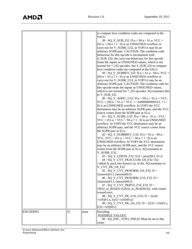
Revision 1.0 September 19, 2012
© 2012 Advanced Micro Devices, Inc. Proprietary 132
to compare how condition codes are computed in the
SALU.
38 - SQ_V_SUB_I32: D.u = S0.u - S1.u. VCC =
(S1.u > S0.u ? 1 : 0) is an UNSIGNED overflow or
carry-out for V_SUBB_U32, in VOP3 it may be an
arbitrary SGPR-pair. CAUTION: The condition code
behaviour for this opcode is inconsistent with
S_SUB_I32; the carry-out behaviour for this opcode
treats the inputs as UNSIGNED values, which is not
normal for *_I32 opcodes. See S_SUB_I32 to compare
how condition codes are computed in the SALU.
39 - SQ_V_SUBREV_I32: D.u = S1.u - S0.u. VCC =
(S0.u > S1.u ? 1 : 0) is an UNSIGNED overflow or
carry-out for V_SUBB_U32, in VOP3 it may be an
arbitrary SGPR-pair. CAUTION: The condition code for
this opcode treats the inputs as UNSIGNED values,
which is not normal for *_I32 opcodes. SQ translates this
to V_SUB_I32.
40 - SQ_V_ADDC_U32: D.u = S0.u + S1.u + VCC.
VCC = (S0.u + S1.u + VCC >= 0x800000000ULL ? 1 :
0) is an UNSIGNED overflow. In VOP3 the VCC
destination may be an arbitrary SGPR-pair, and the VCC
source comes from the SGPR-pair at S2.u.
41 - SQ_V_SUBB_U32: D.u = S0.u - S1.u - VCC.
VCC = (S1.u + VCC > S0.u ? 1 : 0) is an UNSIGNED
overflow. In VOP3 the VCC destination may be an
arbitrary SGPR-pair, and the VCC source comes from
the SGPR-pair at S2.u.
42 - SQ_V_SUBBREV_U32: D.u = S1.u - S0.u -
VCC. VCC = (S1.u + VCC > S0.u ? 1 : 0) is an
UNSIGNED overflow. In VOP3 the VCC destination
may be an arbitrary SGPR-pair, and the VCC source
comes from the SGPR-pair at S2.u. SQ translates to
V_SUBB_U32.
43 - SQ_V_LDEXP_F32: D.d = pow(S0.f, S1.i)
44 - SQ_V_CVT_PKACCUM_U8_F32: f32-
>u8(s0.f), pack into byte(s1.u), of dst. SQ translates to
V_CVT_PK_U8_F32
45 - SQ_V_CVT_PKNORM_I16_F32: D =
{(snorm)S1.f, (snorm)S0.f}
46 - SQ_V_CVT_PKNORM_U16_F32: D =
{(unorm)S1.f, (unorm)S0.f}
47 - SQ_V_CVT_PKRTZ_F16_F32: D =
{flt32_to_flt16(S1.f),flt32_to_flt16(S0.f)}, with round-
toward-zero.
48 - SQ_V_CVT_PK_U16_U32: D = {(u32-
>u16)S1.u, (u32->u16)S0.u}
49 - SQ_V_CVT_PK_I16_I32: D = {(i32->i16)S1.i,
(i32->i16)S0.i}
ENCODING 31 none Encoding.
POSSIBLE VALUES:
00 - SQ_ENC_VOP2_FIELD: Must be set to this
value.

Revision 1.0 September 19, 2012
© 2012 Advanced Micro Devices, Inc. Proprietary 133
SQ_UC:SQ_VOP3_0 · [R/W] · 32 bits · Access: 32 · GpuF0MMReg:0x8dfc
DESCRIPTION: Vector instruction taking three inputs and producing one output - first word, non-VCC case.
Field Name Bits Default Description
VDST 7:0 none Destination for instruction.
POSSIBLE VALUES:
00 - SQ_VGPR: Vector GPR 0. Increment from here
for additional GPRs. There are NUM_VGPR VGPRs in
total.
ABS 10:8 none If ABS[N] set, take the floating-point absolute value of
the N`th input operand. This is applied before negation.
CLAMP 11 none If set, clamp output to [0.0, 1.0]. Applied after output
modifier.
OP 25:17 none Opcode.
POSSIBLE VALUES:
00 - SQ_V_OPC_OFFSET: Offset to add to any
VOPC opcodes when they need to use the VOP3
encoding. For example, SQ_V_OP1_OFFSET +
SQ_V_CMP_EQ generates the VOP3 version of
CMP_EQ.
256 - SQ_V_OP2_OFFSET: Offset to add to any
VOP2 opcodes when they need to use the VOP3
encoding. For example, SQ_V_OP1_OFFSET +
SQ_V_ADD_F32 generates the VOP3 version of ADD.
320 - SQ_V_MAD_LEGACY_F32: D.f = S0.f * S1.f
+ S2.f (DX9 rules, 0.0 * x = 0.0).
321 - SQ_V_MAD_F32: D.f = S0.f * S1.f + S2.f.
322 - SQ_V_MAD_I32_I24: D.i = S0.i[23:0] *
S1.i[23:0] + S2.i.
323 - SQ_V_MAD_U32_U24: D.u = S0.u[23:0] *
S1.u[23:0] + S2.u.
324 - SQ_V_CUBEID_F32: D.f = cubemap face ID
({0.0, 1.0, ..., 5.0}). XYZ coordinate is given in (S0.f,
S1.f, S2.f).
325 - SQ_V_CUBESC_F32: D.f = cubemap S
coordinate. XYZ coordinate is given in (S0.f, S1.f, S2.f).
326 - SQ_V_CUBETC_F32: D.f = cubemap T
coordinate. XYZ coordinate is given in (S0.f, S1.f, S2.f).
327 - SQ_V_CUBEMA_F32: D.f = 2.0 * cubemap
major axis. XYZ coordinate is given in (S0.f, S1.f, S2.f).
328 - SQ_V_BFE_U32: D.u = (S0.u>>S1.u[4:0]) &
((1<<S2.u[4:0])-1); bitfield extract, S0=data,
S1=field_offset, S2=field_width.
329 - SQ_V_BFE_I32: D.i = (S0.i>>S1.u[4:0]) &
((1<<S2.u[4:0])-1); bitfield extract, S0=data,
S1=field_offset, S2=field_width.
330 - SQ_V_BFI_B32: D.u = (S0.u & S1.u) | (~S0.u
& S2.u); bitfield insert.
331 - SQ_V_FMA_F32: D.f = S0.f * S1.f + S2.f.
332 - SQ_V_FMA_F64: D.d = S0.d * S1.d + S2.d.
333 - SQ_V_LERP_U8: D.u = ((S0.u[31:24] +
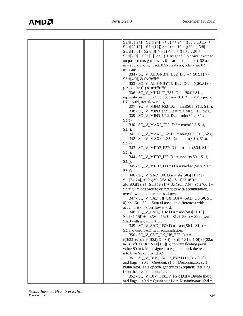
Revision 1.0 September 19, 2012
© 2012 Advanced Micro Devices, Inc. Proprietary 134
S1.u[31:24] + S2.u[24]) >> 1) << 24 + ((S0.u[23:16] +
S1.u[23:16] + S2.u[16]) >> 1) << 16 + ((S0.u[15:8] +
S1.u[15:8] + S2.u[8]) >> 1) << 8 + ((S0.u[7:0] +
S1.u[7:0] + S2.u[0]) >> 1). Unsigned 8-bit pixel average
on packed unsigned bytes (linear interpolation). S2 acts
as a round mode; if set, 0.5 rounds up, otherwise 0.5
truncates.
334 - SQ_V_ALIGNBIT_B32: D.u = ({S0,S1} >>
S2.u[4:0]) & 0xffffffff.
335 - SQ_V_ALIGNBYTE_B32: D.u = ({S0,S1} >>
(8*S2.u[4:0])) & 0xffffffff.
336 - SQ_V_MULLIT_F32: D.f = S0.f * S1.f,
replicate result into 4 components (0.0 * x = 0.0; special
INF, NaN, overflow rules).
337 - SQ_V_MIN3_F32: D.f = min(S0.f, S1.f, S2.f).
338 - SQ_V_MIN3_I32: D.i = min(S0.i, S1.i, S2.i).
339 - SQ_V_MIN3_U32: D.u = min(S0.u, S1.u,
S2.u).
340 - SQ_V_MAX3_F32: D.f = max(S0.f, S1.f,
S2.f).
341 - SQ_V_MAX3_I32: D.i = max(S0.i, S1.i, S2.i).
342 - SQ_V_MAX3_U32: D.u = max(S0.u, S1.u,
S2.u).
343 - SQ_V_MED3_F32: D.f = median(S0.f, S1.f,
S2.f).
344 - SQ_V_MED3_I32: D.i = median(S0.i, S1.i,
S2.i).
345 - SQ_V_MED3_U32: D.u = median(S0.u, S1.u,
S2.u).
346 - SQ_V_SAD_U8: D.u = abs(S0.i[31:24] -
S1.i[31:24]) + abs(S0.i[23:16] - S1.i[23:16]) +
abs(S0.i[15:8] - S1.i[15:8]) + abs(S0.i[7:0] - S1.i[7:0]) +
S2.u; Sum of absolute differences with accumulation,
overflow into upper bits is allowed.
347 - SQ_V_SAD_HI_U8: D.u = (SAD_U8(S0, S1,
0) << 16) + S2.u; Sum of absolute differences with
accumulation, overflow is lost.
348 - SQ_V_SAD_U16: D.u = abs(S0.i[31:16] -
S1.i[31:16]) + abs(S0.i[15:0] - S1.i[15:0]) + S2.u; word
SAD with accumulation.
349 - SQ_V_SAD_U32: D.u = abs(S0.i - S1.i) +
S2.u; dword SAD with accumulation.
350 - SQ_V_CVT_PK_U8_F32: D.u =
((flt32_to_uint8(S0.f) & 0xff) << (8 * S1.u[1:0])) | (S2.u
& ~(0xff << (8 * S1.u[1:0]))); convert floating point
value S0 to 8-bit unsigned integer and pack the result
into byte S1 of dword S2.
351 - SQ_V_DIV_FIXUP_F32: D.f = Divide fixup
and flags -- s0.f = Quotient, s1.f = Denominator, s2.f =
Numerator. This opcode generates exceptions resulting
from the division operation.
352 - SQ_V_DIV_FIXUP_F64: D.d = Divide fixup
and flags -- s0.d = Quotient, s1.d = Denominator, s2.d =

Revision 1.0 September 19, 2012
© 2012 Advanced Micro Devices, Inc. Proprietary 135
Numerator. This opcode generates exceptions resulting
from the division operation.
353 - SQ_V_LSHL_B64: D.u64 = S0.u64 <<
S1.u[5:0].
354 - SQ_V_LSHR_B64: D.u64 = S0.u64 >>
S1.u[5:0].
355 - SQ_V_ASHR_I64: D.u64 = S0.u64 >>
S1.u[5:0].
356 - SQ_V_ADD_F64: D.d = S0.d + S1.d.
357 - SQ_V_MUL_F64: D.d = S0.d * S1.d.
358 - SQ_V_MIN_F64: D.d = min(S0.d, S1.d).
359 - SQ_V_MAX_F64: D.d = max(S0.d, S1.d).
360 - SQ_V_LDEXP_F64: D.d = pow(S0.d,
S1.i[31:0]).
361 - SQ_V_MUL_LO_U32: D.u = S0.u * S1.u.
362 - SQ_V_MUL_HI_U32: D.u = (S0.u * S1.u) >>
32.
363 - SQ_V_MUL_LO_I32: D.i = S0.i * S1.i.
364 - SQ_V_MUL_HI_I32: D.i = (S0.i * S1.i) >> 32.
365 - SQ_V_DIV_SCALE_F32: {vcc,D.f} = Divide
preop and flags -- s0.f = Quotient, s1.f = Denominator,
s2.f = Numerator -- s0 must equal s1 or s2. Given a
numerator and denominator, this opcode will
appropriately scale inputs for division to avoid
subnormal terms during Newton-Raphson correction
algorithm. This opcode producses a VCC flag for post-
scale of quotient.
366 - SQ_V_DIV_SCALE_F64: {vcc,D.d} = Divide
preop and flags -- s0.d = Quotient, s1.d = Denominator,
s2.d = Numerator -- s0 must equal s1 or s2. Given a
numerator and denominator, this opcode will
appropriately scale inputs for division to avoid
subnormal terms during Newton-Raphson correction
algorithm. This opcode producses a VCC flag for post-
scale of quotient.
367 - SQ_V_DIV_FMAS_F32: D.f = Special case
divide FMA with scale and flags(s0.f = Quotient, s1.f =
Denominator, s2.f = Numerator)
368 - SQ_V_DIV_FMAS_F64: D.d = Special case
divide FMA with scale and flags(s0.d = Quotient, s1.d =
Denominator, s2.d = Numerator)
369 - SQ_V_MSAD_U8: D.u = Masked Byte SAD
with accum_lo(S0.u, S1.u, S2.u)
370 - SQ_V_QSAD_PK_U16_U8: D.u = Quad-Byte
SAD with 16-bit packed accum_lo/hi(S0.u[63:0],
S1.u[31:0], S2.u[63:0])
371 - SQ_V_MQSAD_PK_U16_U8: D.u = Masked
Quad-Byte SAD with 16-bit packed
accum_lo/hi(S0.u[63:0], S1.u[31:0], S2.u[63:0])
372 - SQ_V_TRIG_PREOP_F64: D.d = Look Up
2/PI (S0.d) with segment select S1.u[4:0]. This operation
returns an aligned, double precision segment of 2/PI
needed to do range reduction on S0.d (double-precision

Revision 1.0 September 19, 2012
© 2012 Advanced Micro Devices, Inc. Proprietary 136
value). Multiple segments can be specified through
S1.u[4:0]. Rounding is always round-to-zero. Large
inputs (exp > 1968) are scaled to avoid loss of precision
through denormalization.
373 - SQ_V_MQSAD_U32_U8: D.u128 = Masked
Quad-Byte SAD with 32-bit accum_lo/hi(S0.u[63:0],
S1.u[31:0], S2.u[127:0])
374 - SQ_V_MAD_U64_U32: {vcc_out,D.u64} =
S0.u32 * S1.u32 + S2.u64.
375 - SQ_V_MAD_I64_I32: {vcc_out,D.i64} =
S0.i32 * S1.i32 + S2.i64.
384 - SQ_V_OP1_OFFSET: Offset to add to any
VOP1 opcodes when they need to use the VOP3
encoding. For example, SQ_V_OP1_OFFSET +
SQ_V_MOV_B32 generates the VOP3 version of MOV.
ENCODING 31:26 none Encoding.
POSSIBLE VALUES:
52 - SQ_ENC_VOP3_FIELD: Must be set to this
value.
SQ_UC:SQ_VOP3_0_SDST_ENC · [R/W] · 32 bits · Access: 32 · GpuF0MMReg:0x8dfc
DESCRIPTION: Vector instruction taking three inputs and producing one output - first word, VCC case.
Field Name Bits Default Description
VDST 7:0 none Destination for instruction.
POSSIBLE VALUES:
00 - SQ_VGPR: Vector GPR 0. Increment from here
for additional GPRs. There are NUM_VGPR VGPRs in
total.
SDST 14:8 none Destination for compare result.
POSSIBLE VALUES:
00 - SQ_SGPR: Scalar GPR 0. Increment from here
for additional GPRs. There are NUM_SGPR SGPRs in
total.
104 - SQ_FLAT_SCRATCH_LO: {13`d0,
size[18:0]}
105 - SQ_FLAT_SCRATCH_HI: {8`d0,
offset[31:8]}
106 - SQ_VCC_LO: vcc[31:0]
107 - SQ_VCC_HI: vcc[63:32]
108 - SQ_TBA_LO: Trap handler base address,
[31:0]
109 - SQ_TBA_HI: Trap handler base address,
[63:32]
110 - SQ_TMA_LO: Pointer to data in memory used
by trap handler.
111 - SQ_TMA_HI: Pointer to data in memory used
by trap handler.
112 - SQ_TTMP0: Trap handler temps (privileged).
Increment from here for additional TTMPs. There are
NUM_TTMP TTMPs in total. {TTMP1,TTMP0} =
PC_save{hi,lo}.

Revision 1.0 September 19, 2012
© 2012 Advanced Micro Devices, Inc. Proprietary 137
113 - SQ_TTMP1: Trap handler temps (privileged).
114 - SQ_TTMP2: Trap handler temps (privileged).
115 - SQ_TTMP3: Trap handler temps (privileged).
116 - SQ_TTMP4: Trap handler temps (privileged).
117 - SQ_TTMP5: Trap handler temps (privileged).
118 - SQ_TTMP6: Trap handler temps (privileged).
119 - SQ_TTMP7: Trap handler temps (privileged).
120 - SQ_TTMP8: Trap handler temps (privileged).
121 - SQ_TTMP9: Trap handler temps (privileged).
122 - SQ_TTMP10: Trap handler temps (privileged).
123 - SQ_TTMP11: Trap handler temps (privileged).
OP 25:17 none Opcode.
POSSIBLE VALUES:
00 - SQ_V_OPC_OFFSET: Offset to add to any
VOPC opcodes when they need to use the VOP3
encoding. For example, SQ_V_OP1_OFFSET +
SQ_V_CMP_EQ generates the VOP3 version of
CMP_EQ.
256 - SQ_V_OP2_OFFSET: Offset to add to any
VOP2 opcodes when they need to use the VOP3
encoding. For example, SQ_V_OP1_OFFSET +
SQ_V_ADD_F32 generates the VOP3 version of ADD.
320 - SQ_V_MAD_LEGACY_F32: D.f = S0.f * S1.f
+ S2.f (DX9 rules, 0.0 * x = 0.0).
321 - SQ_V_MAD_F32: D.f = S0.f * S1.f + S2.f.
322 - SQ_V_MAD_I32_I24: D.i = S0.i[23:0] *
S1.i[23:0] + S2.i.
323 - SQ_V_MAD_U32_U24: D.u = S0.u[23:0] *
S1.u[23:0] + S2.u.
324 - SQ_V_CUBEID_F32: D.f = cubemap face ID
({0.0, 1.0, ..., 5.0}). XYZ coordinate is given in (S0.f,
S1.f, S2.f).
325 - SQ_V_CUBESC_F32: D.f = cubemap S
coordinate. XYZ coordinate is given in (S0.f, S1.f, S2.f).
326 - SQ_V_CUBETC_F32: D.f = cubemap T
coordinate. XYZ coordinate is given in (S0.f, S1.f, S2.f).
327 - SQ_V_CUBEMA_F32: D.f = 2.0 * cubemap
major axis. XYZ coordinate is given in (S0.f, S1.f, S2.f).
328 - SQ_V_BFE_U32: D.u = (S0.u>>S1.u[4:0]) &
((1<<S2.u[4:0])-1); bitfield extract, S0=data,
S1=field_offset, S2=field_width.
329 - SQ_V_BFE_I32: D.i = (S0.i>>S1.u[4:0]) &
((1<<S2.u[4:0])-1); bitfield extract, S0=data,
S1=field_offset, S2=field_width.
330 - SQ_V_BFI_B32: D.u = (S0.u & S1.u) | (~S0.u
& S2.u); bitfield insert.
331 - SQ_V_FMA_F32: D.f = S0.f * S1.f + S2.f.
332 - SQ_V_FMA_F64: D.d = S0.d * S1.d + S2.d.
333 - SQ_V_LERP_U8: D.u = ((S0.u[31:24] +
S1.u[31:24] + S2.u[24]) >> 1) << 24 + ((S0.u[23:16] +
S1.u[23:16] + S2.u[16]) >> 1) << 16 + ((S0.u[15:8] +
S1.u[15:8] + S2.u[8]) >> 1) << 8 + ((S0.u[7:0] +
S1.u[7:0] + S2.u[0]) >> 1). Unsigned 8-bit pixel average

Revision 1.0 September 19, 2012
© 2012 Advanced Micro Devices, Inc. Proprietary 138
on packed unsigned bytes (linear interpolation). S2 acts
as a round mode; if set, 0.5 rounds up, otherwise 0.5
truncates.
334 - SQ_V_ALIGNBIT_B32: D.u = ({S0,S1} >>
S2.u[4:0]) & 0xffffffff.
335 - SQ_V_ALIGNBYTE_B32: D.u = ({S0,S1} >>
(8*S2.u[4:0])) & 0xffffffff.
336 - SQ_V_MULLIT_F32: D.f = S0.f * S1.f,
replicate result into 4 components (0.0 * x = 0.0; special
INF, NaN, overflow rules).
337 - SQ_V_MIN3_F32: D.f = min(S0.f, S1.f, S2.f).
338 - SQ_V_MIN3_I32: D.i = min(S0.i, S1.i, S2.i).
339 - SQ_V_MIN3_U32: D.u = min(S0.u, S1.u,
S2.u).
340 - SQ_V_MAX3_F32: D.f = max(S0.f, S1.f,
S2.f).
341 - SQ_V_MAX3_I32: D.i = max(S0.i, S1.i, S2.i).
342 - SQ_V_MAX3_U32: D.u = max(S0.u, S1.u,
S2.u).
343 - SQ_V_MED3_F32: D.f = median(S0.f, S1.f,
S2.f).
344 - SQ_V_MED3_I32: D.i = median(S0.i, S1.i,
S2.i).
345 - SQ_V_MED3_U32: D.u = median(S0.u, S1.u,
S2.u).
346 - SQ_V_SAD_U8: D.u = abs(S0.i[31:24] -
S1.i[31:24]) + abs(S0.i[23:16] - S1.i[23:16]) +
abs(S0.i[15:8] - S1.i[15:8]) + abs(S0.i[7:0] - S1.i[7:0]) +
S2.u; Sum of absolute differences with accumulation,
overflow into upper bits is allowed.
347 - SQ_V_SAD_HI_U8: D.u = (SAD_U8(S0, S1,
0) << 16) + S2.u; Sum of absolute differences with
accumulation, overflow is lost.
348 - SQ_V_SAD_U16: D.u = abs(S0.i[31:16] -
S1.i[31:16]) + abs(S0.i[15:0] - S1.i[15:0]) + S2.u; word
SAD with accumulation.
349 - SQ_V_SAD_U32: D.u = abs(S0.i - S1.i) +
S2.u; dword SAD with accumulation.
350 - SQ_V_CVT_PK_U8_F32: D.u =
((flt32_to_uint8(S0.f) & 0xff) << (8 * S1.u[1:0])) | (S2.u
& ~(0xff << (8 * S1.u[1:0]))); convert floating point
value S0 to 8-bit unsigned integer and pack the result
into byte S1 of dword S2.
351 - SQ_V_DIV_FIXUP_F32: D.f = Divide fixup
and flags -- s0.f = Quotient, s1.f = Denominator, s2.f =
Numerator. This opcode generates exceptions resulting
from the division operation.
352 - SQ_V_DIV_FIXUP_F64: D.d = Divide fixup
and flags -- s0.d = Quotient, s1.d = Denominator, s2.d =
Numerator. This opcode generates exceptions resulting
from the division operation.
353 - SQ_V_LSHL_B64: D.u64 = S0.u64 <<
S1.u[5:0].

Revision 1.0 September 19, 2012
© 2012 Advanced Micro Devices, Inc. Proprietary 139
354 - SQ_V_LSHR_B64: D.u64 = S0.u64 >>
S1.u[5:0].
355 - SQ_V_ASHR_I64: D.u64 = S0.u64 >>
S1.u[5:0].
356 - SQ_V_ADD_F64: D.d = S0.d + S1.d.
357 - SQ_V_MUL_F64: D.d = S0.d * S1.d.
358 - SQ_V_MIN_F64: D.d = min(S0.d, S1.d).
359 - SQ_V_MAX_F64: D.d = max(S0.d, S1.d).
360 - SQ_V_LDEXP_F64: D.d = pow(S0.d,
S1.i[31:0]).
361 - SQ_V_MUL_LO_U32: D.u = S0.u * S1.u.
362 - SQ_V_MUL_HI_U32: D.u = (S0.u * S1.u) >>
32.
363 - SQ_V_MUL_LO_I32: D.i = S0.i * S1.i.
364 - SQ_V_MUL_HI_I32: D.i = (S0.i * S1.i) >> 32.
365 - SQ_V_DIV_SCALE_F32: {vcc,D.f} = Divide
preop and flags -- s0.f = Quotient, s1.f = Denominator,
s2.f = Numerator -- s0 must equal s1 or s2. Given a
numerator and denominator, this opcode will
appropriately scale inputs for division to avoid
subnormal terms during Newton-Raphson correction
algorithm. This opcode producses a VCC flag for post-
scale of quotient.
366 - SQ_V_DIV_SCALE_F64: {vcc,D.d} = Divide
preop and flags -- s0.d = Quotient, s1.d = Denominator,
s2.d = Numerator -- s0 must equal s1 or s2. Given a
numerator and denominator, this opcode will
appropriately scale inputs for division to avoid
subnormal terms during Newton-Raphson correction
algorithm. This opcode producses a VCC flag for post-
scale of quotient.
367 - SQ_V_DIV_FMAS_F32: D.f = Special case
divide FMA with scale and flags(s0.f = Quotient, s1.f =
Denominator, s2.f = Numerator)
368 - SQ_V_DIV_FMAS_F64: D.d = Special case
divide FMA with scale and flags(s0.d = Quotient, s1.d =
Denominator, s2.d = Numerator)
369 - SQ_V_MSAD_U8: D.u = Masked Byte SAD
with accum_lo(S0.u, S1.u, S2.u)
370 - SQ_V_QSAD_PK_U16_U8: D.u = Quad-Byte
SAD with 16-bit packed accum_lo/hi(S0.u[63:0],
S1.u[31:0], S2.u[63:0])
371 - SQ_V_MQSAD_PK_U16_U8: D.u = Masked
Quad-Byte SAD with 16-bit packed
accum_lo/hi(S0.u[63:0], S1.u[31:0], S2.u[63:0])
372 - SQ_V_TRIG_PREOP_F64: D.d = Look Up
2/PI (S0.d) with segment select S1.u[4:0]. This operation
returns an aligned, double precision segment of 2/PI
needed to do range reduction on S0.d (double-precision
value). Multiple segments can be specified through
S1.u[4:0]. Rounding is always round-to-zero. Large
inputs (exp > 1968) are scaled to avoid loss of precision
through denormalization.
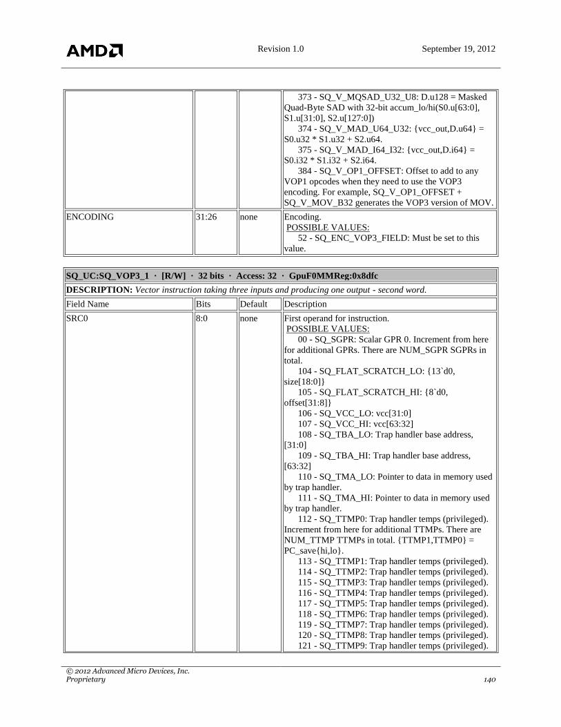
Revision 1.0 September 19, 2012
© 2012 Advanced Micro Devices, Inc. Proprietary 140
373 - SQ_V_MQSAD_U32_U8: D.u128 = Masked
Quad-Byte SAD with 32-bit accum_lo/hi(S0.u[63:0],
S1.u[31:0], S2.u[127:0])
374 - SQ_V_MAD_U64_U32: {vcc_out,D.u64} =
S0.u32 * S1.u32 + S2.u64.
375 - SQ_V_MAD_I64_I32: {vcc_out,D.i64} =
S0.i32 * S1.i32 + S2.i64.
384 - SQ_V_OP1_OFFSET: Offset to add to any
VOP1 opcodes when they need to use the VOP3
encoding. For example, SQ_V_OP1_OFFSET +
SQ_V_MOV_B32 generates the VOP3 version of MOV.
ENCODING 31:26 none Encoding.
POSSIBLE VALUES:
52 - SQ_ENC_VOP3_FIELD: Must be set to this
value.
SQ_UC:SQ_VOP3_1 · [R/W] · 32 bits · Access: 32 · GpuF0MMReg:0x8dfc
DESCRIPTION: Vector instruction taking three inputs and producing one output - second word.
Field Name Bits Default Description
SRC0 8:0 none First operand for instruction.
POSSIBLE VALUES:
00 - SQ_SGPR: Scalar GPR 0. Increment from here
for additional GPRs. There are NUM_SGPR SGPRs in
total.
104 - SQ_FLAT_SCRATCH_LO: {13`d0,
size[18:0]}
105 - SQ_FLAT_SCRATCH_HI: {8`d0,
offset[31:8]}
106 - SQ_VCC_LO: vcc[31:0]
107 - SQ_VCC_HI: vcc[63:32]
108 - SQ_TBA_LO: Trap handler base address,
[31:0]
109 - SQ_TBA_HI: Trap handler base address,
[63:32]
110 - SQ_TMA_LO: Pointer to data in memory used
by trap handler.
111 - SQ_TMA_HI: Pointer to data in memory used
by trap handler.
112 - SQ_TTMP0: Trap handler temps (privileged).
Increment from here for additional TTMPs. There are
NUM_TTMP TTMPs in total. {TTMP1,TTMP0} =
PC_save{hi,lo}.
113 - SQ_TTMP1: Trap handler temps (privileged).
114 - SQ_TTMP2: Trap handler temps (privileged).
115 - SQ_TTMP3: Trap handler temps (privileged).
116 - SQ_TTMP4: Trap handler temps (privileged).
117 - SQ_TTMP5: Trap handler temps (privileged).
118 - SQ_TTMP6: Trap handler temps (privileged).
119 - SQ_TTMP7: Trap handler temps (privileged).
120 - SQ_TTMP8: Trap handler temps (privileged).
121 - SQ_TTMP9: Trap handler temps (privileged).
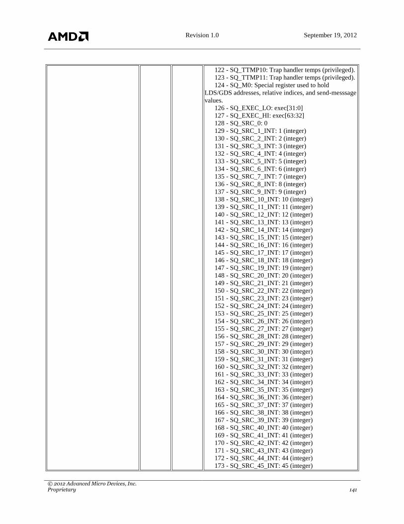
Revision 1.0 September 19, 2012
© 2012 Advanced Micro Devices, Inc. Proprietary 141
122 - SQ_TTMP10: Trap handler temps (privileged).
123 - SQ_TTMP11: Trap handler temps (privileged).
124 - SQ_M0: Special register used to hold
LDS/GDS addresses, relative indices, and send-messsage
values.
126 - SQ_EXEC_LO: exec[31:0]
127 - SQ_EXEC_HI: exec[63:32]
128 - SQ_SRC_0: 0
129 - SQ_SRC_1_INT: 1 (integer)
130 - SQ_SRC_2_INT: 2 (integer)
131 - SQ_SRC_3_INT: 3 (integer)
132 - SQ_SRC_4_INT: 4 (integer)
133 - SQ_SRC_5_INT: 5 (integer)
134 - SQ_SRC_6_INT: 6 (integer)
135 - SQ_SRC_7_INT: 7 (integer)
136 - SQ_SRC_8_INT: 8 (integer)
137 - SQ_SRC_9_INT: 9 (integer)
138 - SQ_SRC_10_INT: 10 (integer)
139 - SQ_SRC_11_INT: 11 (integer)
140 - SQ_SRC_12_INT: 12 (integer)
141 - SQ_SRC_13_INT: 13 (integer)
142 - SQ_SRC_14_INT: 14 (integer)
143 - SQ_SRC_15_INT: 15 (integer)
144 - SQ_SRC_16_INT: 16 (integer)
145 - SQ_SRC_17_INT: 17 (integer)
146 - SQ_SRC_18_INT: 18 (integer)
147 - SQ_SRC_19_INT: 19 (integer)
148 - SQ_SRC_20_INT: 20 (integer)
149 - SQ_SRC_21_INT: 21 (integer)
150 - SQ_SRC_22_INT: 22 (integer)
151 - SQ_SRC_23_INT: 23 (integer)
152 - SQ_SRC_24_INT: 24 (integer)
153 - SQ_SRC_25_INT: 25 (integer)
154 - SQ_SRC_26_INT: 26 (integer)
155 - SQ_SRC_27_INT: 27 (integer)
156 - SQ_SRC_28_INT: 28 (integer)
157 - SQ_SRC_29_INT: 29 (integer)
158 - SQ_SRC_30_INT: 30 (integer)
159 - SQ_SRC_31_INT: 31 (integer)
160 - SQ_SRC_32_INT: 32 (integer)
161 - SQ_SRC_33_INT: 33 (integer)
162 - SQ_SRC_34_INT: 34 (integer)
163 - SQ_SRC_35_INT: 35 (integer)
164 - SQ_SRC_36_INT: 36 (integer)
165 - SQ_SRC_37_INT: 37 (integer)
166 - SQ_SRC_38_INT: 38 (integer)
167 - SQ_SRC_39_INT: 39 (integer)
168 - SQ_SRC_40_INT: 40 (integer)
169 - SQ_SRC_41_INT: 41 (integer)
170 - SQ_SRC_42_INT: 42 (integer)
171 - SQ_SRC_43_INT: 43 (integer)
172 - SQ_SRC_44_INT: 44 (integer)
173 - SQ_SRC_45_INT: 45 (integer)

Revision 1.0 September 19, 2012
© 2012 Advanced Micro Devices, Inc. Proprietary 142
174 - SQ_SRC_46_INT: 46 (integer)
175 - SQ_SRC_47_INT: 47 (integer)
176 - SQ_SRC_48_INT: 48 (integer)
177 - SQ_SRC_49_INT: 49 (integer)
178 - SQ_SRC_50_INT: 50 (integer)
179 - SQ_SRC_51_INT: 51 (integer)
180 - SQ_SRC_52_INT: 52 (integer)
181 - SQ_SRC_53_INT: 53 (integer)
182 - SQ_SRC_54_INT: 54 (integer)
183 - SQ_SRC_55_INT: 55 (integer)
184 - SQ_SRC_56_INT: 56 (integer)
185 - SQ_SRC_57_INT: 57 (integer)
186 - SQ_SRC_58_INT: 58 (integer)
187 - SQ_SRC_59_INT: 59 (integer)
188 - SQ_SRC_60_INT: 60 (integer)
189 - SQ_SRC_61_INT: 61 (integer)
190 - SQ_SRC_62_INT: 62 (integer)
191 - SQ_SRC_63_INT: 63 (integer)
192 - SQ_SRC_64_INT: 64 (integer)
193 - SQ_SRC_M_1_INT: -1 (integer)
194 - SQ_SRC_M_2_INT: -2 (integer)
195 - SQ_SRC_M_3_INT: -3 (integer)
196 - SQ_SRC_M_4_INT: -4 (integer)
197 - SQ_SRC_M_5_INT: -5 (integer)
198 - SQ_SRC_M_6_INT: -6 (integer)
199 - SQ_SRC_M_7_INT: -7 (integer)
200 - SQ_SRC_M_8_INT: -8 (integer)
201 - SQ_SRC_M_9_INT: -9 (integer)
202 - SQ_SRC_M_10_INT: -10 (integer)
203 - SQ_SRC_M_11_INT: -11 (integer)
204 - SQ_SRC_M_12_INT: -12 (integer)
205 - SQ_SRC_M_13_INT: -13 (integer)
206 - SQ_SRC_M_14_INT: -14 (integer)
207 - SQ_SRC_M_15_INT: -15 (integer)
208 - SQ_SRC_M_16_INT: -16 (integer)
240 - SQ_SRC_0_5: 0.5
241 - SQ_SRC_M_0_5: -0.5
242 - SQ_SRC_1: 1.0
243 - SQ_SRC_M_1: -1.0
244 - SQ_SRC_2: 2.0
245 - SQ_SRC_M_2: -2.0
246 - SQ_SRC_4: 4.0
247 - SQ_SRC_M_4: -4.0
251 - SQ_SRC_VCCZ: vector-condition-code-is-
zero
252 - SQ_SRC_EXECZ: execute-mask-is-zero
253 - SQ_SRC_SCC: scalar condition code
254 - SQ_SRC_LDS_DIRECT: use LDS direct to
supply 32-bit value (address from M0 register).
256 - SQ_SRC_VGPR: Vector GPR 0. Increment
from here for additional GPRs. There are NUM_VGPR
VGPRs in total. You may use the constant
SQ_SRC_VGPR_BIT to set or clear the high order bit

Revision 1.0 September 19, 2012
© 2012 Advanced Micro Devices, Inc. Proprietary 143
for vector GPRs in this operand.
SRC1 17:9 none Second operand for instruction.
POSSIBLE VALUES:
00 - SQ_SGPR: Scalar GPR 0. Increment from here
for additional GPRs. There are NUM_SGPR SGPRs in
total.
104 - SQ_FLAT_SCRATCH_LO: {13`d0,
size[18:0]}
105 - SQ_FLAT_SCRATCH_HI: {8`d0,
offset[31:8]}
106 - SQ_VCC_LO: vcc[31:0]
107 - SQ_VCC_HI: vcc[63:32]
108 - SQ_TBA_LO: Trap handler base address,
[31:0]
109 - SQ_TBA_HI: Trap handler base address,
[63:32]
110 - SQ_TMA_LO: Pointer to data in memory used
by trap handler.
111 - SQ_TMA_HI: Pointer to data in memory used
by trap handler.
112 - SQ_TTMP0: Trap handler temps (privileged).
Increment from here for additional TTMPs. There are
NUM_TTMP TTMPs in total. {TTMP1,TTMP0} =
PC_save{hi,lo}.
113 - SQ_TTMP1: Trap handler temps (privileged).
114 - SQ_TTMP2: Trap handler temps (privileged).
115 - SQ_TTMP3: Trap handler temps (privileged).
116 - SQ_TTMP4: Trap handler temps (privileged).
117 - SQ_TTMP5: Trap handler temps (privileged).
118 - SQ_TTMP6: Trap handler temps (privileged).
119 - SQ_TTMP7: Trap handler temps (privileged).
120 - SQ_TTMP8: Trap handler temps (privileged).
121 - SQ_TTMP9: Trap handler temps (privileged).
122 - SQ_TTMP10: Trap handler temps (privileged).
123 - SQ_TTMP11: Trap handler temps (privileged).
124 - SQ_M0: Special register used to hold
LDS/GDS addresses, relative indices, and send-messsage
values.
126 - SQ_EXEC_LO: exec[31:0]
127 - SQ_EXEC_HI: exec[63:32]
128 - SQ_SRC_0: 0
129 - SQ_SRC_1_INT: 1 (integer)
130 - SQ_SRC_2_INT: 2 (integer)
131 - SQ_SRC_3_INT: 3 (integer)
132 - SQ_SRC_4_INT: 4 (integer)
133 - SQ_SRC_5_INT: 5 (integer)
134 - SQ_SRC_6_INT: 6 (integer)
135 - SQ_SRC_7_INT: 7 (integer)
136 - SQ_SRC_8_INT: 8 (integer)
137 - SQ_SRC_9_INT: 9 (integer)
138 - SQ_SRC_10_INT: 10 (integer)
139 - SQ_SRC_11_INT: 11 (integer)
140 - SQ_SRC_12_INT: 12 (integer)

Revision 1.0 September 19, 2012
© 2012 Advanced Micro Devices, Inc. Proprietary 144
141 - SQ_SRC_13_INT: 13 (integer)
142 - SQ_SRC_14_INT: 14 (integer)
143 - SQ_SRC_15_INT: 15 (integer)
144 - SQ_SRC_16_INT: 16 (integer)
145 - SQ_SRC_17_INT: 17 (integer)
146 - SQ_SRC_18_INT: 18 (integer)
147 - SQ_SRC_19_INT: 19 (integer)
148 - SQ_SRC_20_INT: 20 (integer)
149 - SQ_SRC_21_INT: 21 (integer)
150 - SQ_SRC_22_INT: 22 (integer)
151 - SQ_SRC_23_INT: 23 (integer)
152 - SQ_SRC_24_INT: 24 (integer)
153 - SQ_SRC_25_INT: 25 (integer)
154 - SQ_SRC_26_INT: 26 (integer)
155 - SQ_SRC_27_INT: 27 (integer)
156 - SQ_SRC_28_INT: 28 (integer)
157 - SQ_SRC_29_INT: 29 (integer)
158 - SQ_SRC_30_INT: 30 (integer)
159 - SQ_SRC_31_INT: 31 (integer)
160 - SQ_SRC_32_INT: 32 (integer)
161 - SQ_SRC_33_INT: 33 (integer)
162 - SQ_SRC_34_INT: 34 (integer)
163 - SQ_SRC_35_INT: 35 (integer)
164 - SQ_SRC_36_INT: 36 (integer)
165 - SQ_SRC_37_INT: 37 (integer)
166 - SQ_SRC_38_INT: 38 (integer)
167 - SQ_SRC_39_INT: 39 (integer)
168 - SQ_SRC_40_INT: 40 (integer)
169 - SQ_SRC_41_INT: 41 (integer)
170 - SQ_SRC_42_INT: 42 (integer)
171 - SQ_SRC_43_INT: 43 (integer)
172 - SQ_SRC_44_INT: 44 (integer)
173 - SQ_SRC_45_INT: 45 (integer)
174 - SQ_SRC_46_INT: 46 (integer)
175 - SQ_SRC_47_INT: 47 (integer)
176 - SQ_SRC_48_INT: 48 (integer)
177 - SQ_SRC_49_INT: 49 (integer)
178 - SQ_SRC_50_INT: 50 (integer)
179 - SQ_SRC_51_INT: 51 (integer)
180 - SQ_SRC_52_INT: 52 (integer)
181 - SQ_SRC_53_INT: 53 (integer)
182 - SQ_SRC_54_INT: 54 (integer)
183 - SQ_SRC_55_INT: 55 (integer)
184 - SQ_SRC_56_INT: 56 (integer)
185 - SQ_SRC_57_INT: 57 (integer)
186 - SQ_SRC_58_INT: 58 (integer)
187 - SQ_SRC_59_INT: 59 (integer)
188 - SQ_SRC_60_INT: 60 (integer)
189 - SQ_SRC_61_INT: 61 (integer)
190 - SQ_SRC_62_INT: 62 (integer)
191 - SQ_SRC_63_INT: 63 (integer)
192 - SQ_SRC_64_INT: 64 (integer)
193 - SQ_SRC_M_1_INT: -1 (integer)

Revision 1.0 September 19, 2012
© 2012 Advanced Micro Devices, Inc. Proprietary 145
194 - SQ_SRC_M_2_INT: -2 (integer)
195 - SQ_SRC_M_3_INT: -3 (integer)
196 - SQ_SRC_M_4_INT: -4 (integer)
197 - SQ_SRC_M_5_INT: -5 (integer)
198 - SQ_SRC_M_6_INT: -6 (integer)
199 - SQ_SRC_M_7_INT: -7 (integer)
200 - SQ_SRC_M_8_INT: -8 (integer)
201 - SQ_SRC_M_9_INT: -9 (integer)
202 - SQ_SRC_M_10_INT: -10 (integer)
203 - SQ_SRC_M_11_INT: -11 (integer)
204 - SQ_SRC_M_12_INT: -12 (integer)
205 - SQ_SRC_M_13_INT: -13 (integer)
206 - SQ_SRC_M_14_INT: -14 (integer)
207 - SQ_SRC_M_15_INT: -15 (integer)
208 - SQ_SRC_M_16_INT: -16 (integer)
240 - SQ_SRC_0_5: 0.5
241 - SQ_SRC_M_0_5: -0.5
242 - SQ_SRC_1: 1.0
243 - SQ_SRC_M_1: -1.0
244 - SQ_SRC_2: 2.0
245 - SQ_SRC_M_2: -2.0
246 - SQ_SRC_4: 4.0
247 - SQ_SRC_M_4: -4.0
251 - SQ_SRC_VCCZ: vector-condition-code-is-
zero
252 - SQ_SRC_EXECZ: execute-mask-is-zero
253 - SQ_SRC_SCC: scalar condition code
254 - SQ_SRC_LDS_DIRECT: use LDS direct to
supply 32-bit value (address from M0 register).
256 - SQ_SRC_VGPR: Vector GPR 0. Increment
from here for additional GPRs. There are NUM_VGPR
VGPRs in total. You may use the constant
SQ_SRC_VGPR_BIT to set or clear the high order bit
for vector GPRs in this operand.
SRC2 26:18 none Third operand for instruction.
POSSIBLE VALUES:
00 - SQ_SGPR: Scalar GPR 0. Increment from here
for additional GPRs. There are NUM_SGPR SGPRs in
total.
104 - SQ_FLAT_SCRATCH_LO: {13`d0,
size[18:0]}
105 - SQ_FLAT_SCRATCH_HI: {8`d0,
offset[31:8]}
106 - SQ_VCC_LO: vcc[31:0]
107 - SQ_VCC_HI: vcc[63:32]
108 - SQ_TBA_LO: Trap handler base address,
[31:0]
109 - SQ_TBA_HI: Trap handler base address,
[63:32]
110 - SQ_TMA_LO: Pointer to data in memory used
by trap handler.
111 - SQ_TMA_HI: Pointer to data in memory used
by trap handler.

Revision 1.0 September 19, 2012
© 2012 Advanced Micro Devices, Inc. Proprietary 146
112 - SQ_TTMP0: Trap handler temps (privileged).
Increment from here for additional TTMPs. There are
NUM_TTMP TTMPs in total. {TTMP1,TTMP0} =
PC_save{hi,lo}.
113 - SQ_TTMP1: Trap handler temps (privileged).
114 - SQ_TTMP2: Trap handler temps (privileged).
115 - SQ_TTMP3: Trap handler temps (privileged).
116 - SQ_TTMP4: Trap handler temps (privileged).
117 - SQ_TTMP5: Trap handler temps (privileged).
118 - SQ_TTMP6: Trap handler temps (privileged).
119 - SQ_TTMP7: Trap handler temps (privileged).
120 - SQ_TTMP8: Trap handler temps (privileged).
121 - SQ_TTMP9: Trap handler temps (privileged).
122 - SQ_TTMP10: Trap handler temps (privileged).
123 - SQ_TTMP11: Trap handler temps (privileged).
124 - SQ_M0: Special register used to hold
LDS/GDS addresses, relative indices, and send-messsage
values.
126 - SQ_EXEC_LO: exec[31:0]
127 - SQ_EXEC_HI: exec[63:32]
128 - SQ_SRC_0: 0
129 - SQ_SRC_1_INT: 1 (integer)
130 - SQ_SRC_2_INT: 2 (integer)
131 - SQ_SRC_3_INT: 3 (integer)
132 - SQ_SRC_4_INT: 4 (integer)
133 - SQ_SRC_5_INT: 5 (integer)
134 - SQ_SRC_6_INT: 6 (integer)
135 - SQ_SRC_7_INT: 7 (integer)
136 - SQ_SRC_8_INT: 8 (integer)
137 - SQ_SRC_9_INT: 9 (integer)
138 - SQ_SRC_10_INT: 10 (integer)
139 - SQ_SRC_11_INT: 11 (integer)
140 - SQ_SRC_12_INT: 12 (integer)
141 - SQ_SRC_13_INT: 13 (integer)
142 - SQ_SRC_14_INT: 14 (integer)
143 - SQ_SRC_15_INT: 15 (integer)
144 - SQ_SRC_16_INT: 16 (integer)
145 - SQ_SRC_17_INT: 17 (integer)
146 - SQ_SRC_18_INT: 18 (integer)
147 - SQ_SRC_19_INT: 19 (integer)
148 - SQ_SRC_20_INT: 20 (integer)
149 - SQ_SRC_21_INT: 21 (integer)
150 - SQ_SRC_22_INT: 22 (integer)
151 - SQ_SRC_23_INT: 23 (integer)
152 - SQ_SRC_24_INT: 24 (integer)
153 - SQ_SRC_25_INT: 25 (integer)
154 - SQ_SRC_26_INT: 26 (integer)
155 - SQ_SRC_27_INT: 27 (integer)
156 - SQ_SRC_28_INT: 28 (integer)
157 - SQ_SRC_29_INT: 29 (integer)
158 - SQ_SRC_30_INT: 30 (integer)
159 - SQ_SRC_31_INT: 31 (integer)
160 - SQ_SRC_32_INT: 32 (integer)

Revision 1.0 September 19, 2012
© 2012 Advanced Micro Devices, Inc. Proprietary 147
161 - SQ_SRC_33_INT: 33 (integer)
162 - SQ_SRC_34_INT: 34 (integer)
163 - SQ_SRC_35_INT: 35 (integer)
164 - SQ_SRC_36_INT: 36 (integer)
165 - SQ_SRC_37_INT: 37 (integer)
166 - SQ_SRC_38_INT: 38 (integer)
167 - SQ_SRC_39_INT: 39 (integer)
168 - SQ_SRC_40_INT: 40 (integer)
169 - SQ_SRC_41_INT: 41 (integer)
170 - SQ_SRC_42_INT: 42 (integer)
171 - SQ_SRC_43_INT: 43 (integer)
172 - SQ_SRC_44_INT: 44 (integer)
173 - SQ_SRC_45_INT: 45 (integer)
174 - SQ_SRC_46_INT: 46 (integer)
175 - SQ_SRC_47_INT: 47 (integer)
176 - SQ_SRC_48_INT: 48 (integer)
177 - SQ_SRC_49_INT: 49 (integer)
178 - SQ_SRC_50_INT: 50 (integer)
179 - SQ_SRC_51_INT: 51 (integer)
180 - SQ_SRC_52_INT: 52 (integer)
181 - SQ_SRC_53_INT: 53 (integer)
182 - SQ_SRC_54_INT: 54 (integer)
183 - SQ_SRC_55_INT: 55 (integer)
184 - SQ_SRC_56_INT: 56 (integer)
185 - SQ_SRC_57_INT: 57 (integer)
186 - SQ_SRC_58_INT: 58 (integer)
187 - SQ_SRC_59_INT: 59 (integer)
188 - SQ_SRC_60_INT: 60 (integer)
189 - SQ_SRC_61_INT: 61 (integer)
190 - SQ_SRC_62_INT: 62 (integer)
191 - SQ_SRC_63_INT: 63 (integer)
192 - SQ_SRC_64_INT: 64 (integer)
193 - SQ_SRC_M_1_INT: -1 (integer)
194 - SQ_SRC_M_2_INT: -2 (integer)
195 - SQ_SRC_M_3_INT: -3 (integer)
196 - SQ_SRC_M_4_INT: -4 (integer)
197 - SQ_SRC_M_5_INT: -5 (integer)
198 - SQ_SRC_M_6_INT: -6 (integer)
199 - SQ_SRC_M_7_INT: -7 (integer)
200 - SQ_SRC_M_8_INT: -8 (integer)
201 - SQ_SRC_M_9_INT: -9 (integer)
202 - SQ_SRC_M_10_INT: -10 (integer)
203 - SQ_SRC_M_11_INT: -11 (integer)
204 - SQ_SRC_M_12_INT: -12 (integer)
205 - SQ_SRC_M_13_INT: -13 (integer)
206 - SQ_SRC_M_14_INT: -14 (integer)
207 - SQ_SRC_M_15_INT: -15 (integer)
208 - SQ_SRC_M_16_INT: -16 (integer)
240 - SQ_SRC_0_5: 0.5
241 - SQ_SRC_M_0_5: -0.5
242 - SQ_SRC_1: 1.0
243 - SQ_SRC_M_1: -1.0
244 - SQ_SRC_2: 2.0

Revision 1.0 September 19, 2012
© 2012 Advanced Micro Devices, Inc. Proprietary 148
245 - SQ_SRC_M_2: -2.0
246 - SQ_SRC_4: 4.0
247 - SQ_SRC_M_4: -4.0
251 - SQ_SRC_VCCZ: vector-condition-code-is-
zero
252 - SQ_SRC_EXECZ: execute-mask-is-zero
253 - SQ_SRC_SCC: scalar condition code
254 - SQ_SRC_LDS_DIRECT: use LDS direct to
supply 32-bit value (address from M0 register).
256 - SQ_SRC_VGPR: Vector GPR 0. Increment
from here for additional GPRs. There are NUM_VGPR
VGPRs in total. You may use the constant
SQ_SRC_VGPR_BIT to set or clear the high order bit
for vector GPRs in this operand.
OMOD 28:27 none Output modifier for instruction. Applied before
clamping.
POSSIBLE VALUES:
00 - SQ_OMOD_OFF: No output modification.
01 - SQ_OMOD_M2: Multiply output by 2.0.
02 - SQ_OMOD_M4: Multiply output by 4.0.
03 - SQ_OMOD_D2: Divide output by 2.0.
NEG 31:29 none If NEG[N] set, take the floating-point negation of the
N`th input operand. This is applied after absolute value.
SQ_UC:SQ_VOPC · [R/W] · 32 bits · Access: 32 · GpuF0MMReg:0x8dfc
DESCRIPTION: Vector instruction taking two inputs and producing a comparison result.
Field Name Bits Default Description
SRC0 8:0 none First operand for instruction.
POSSIBLE VALUES:
00 - SQ_SGPR: Scalar GPR 0. Increment from here
for additional GPRs. There are NUM_SGPR SGPRs in
total.
104 - SQ_FLAT_SCRATCH_LO: {13`d0,
size[18:0]}
105 - SQ_FLAT_SCRATCH_HI: {8`d0,
offset[31:8]}
106 - SQ_VCC_LO: vcc[31:0]
107 - SQ_VCC_HI: vcc[63:32]
108 - SQ_TBA_LO: Trap handler base address,
[31:0]
109 - SQ_TBA_HI: Trap handler base address,
[63:32]
110 - SQ_TMA_LO: Pointer to data in memory used
by trap handler.
111 - SQ_TMA_HI: Pointer to data in memory used
by trap handler.
112 - SQ_TTMP0: Trap handler temps (privileged).
Increment from here for additional TTMPs. There are
NUM_TTMP TTMPs in total. {TTMP1,TTMP0} =
PC_save{hi,lo}.
113 - SQ_TTMP1: Trap handler temps (privileged).

Revision 1.0 September 19, 2012
© 2012 Advanced Micro Devices, Inc. Proprietary 149
114 - SQ_TTMP2: Trap handler temps (privileged).
115 - SQ_TTMP3: Trap handler temps (privileged).
116 - SQ_TTMP4: Trap handler temps (privileged).
117 - SQ_TTMP5: Trap handler temps (privileged).
118 - SQ_TTMP6: Trap handler temps (privileged).
119 - SQ_TTMP7: Trap handler temps (privileged).
120 - SQ_TTMP8: Trap handler temps (privileged).
121 - SQ_TTMP9: Trap handler temps (privileged).
122 - SQ_TTMP10: Trap handler temps (privileged).
123 - SQ_TTMP11: Trap handler temps (privileged).
124 - SQ_M0: Special register used to hold
LDS/GDS addresses, relative indices, and send-messsage
values.
126 - SQ_EXEC_LO: exec[31:0]
127 - SQ_EXEC_HI: exec[63:32]
128 - SQ_SRC_0: 0
129 - SQ_SRC_1_INT: 1 (integer)
130 - SQ_SRC_2_INT: 2 (integer)
131 - SQ_SRC_3_INT: 3 (integer)
132 - SQ_SRC_4_INT: 4 (integer)
133 - SQ_SRC_5_INT: 5 (integer)
134 - SQ_SRC_6_INT: 6 (integer)
135 - SQ_SRC_7_INT: 7 (integer)
136 - SQ_SRC_8_INT: 8 (integer)
137 - SQ_SRC_9_INT: 9 (integer)
138 - SQ_SRC_10_INT: 10 (integer)
139 - SQ_SRC_11_INT: 11 (integer)
140 - SQ_SRC_12_INT: 12 (integer)
141 - SQ_SRC_13_INT: 13 (integer)
142 - SQ_SRC_14_INT: 14 (integer)
143 - SQ_SRC_15_INT: 15 (integer)
144 - SQ_SRC_16_INT: 16 (integer)
145 - SQ_SRC_17_INT: 17 (integer)
146 - SQ_SRC_18_INT: 18 (integer)
147 - SQ_SRC_19_INT: 19 (integer)
148 - SQ_SRC_20_INT: 20 (integer)
149 - SQ_SRC_21_INT: 21 (integer)
150 - SQ_SRC_22_INT: 22 (integer)
151 - SQ_SRC_23_INT: 23 (integer)
152 - SQ_SRC_24_INT: 24 (integer)
153 - SQ_SRC_25_INT: 25 (integer)
154 - SQ_SRC_26_INT: 26 (integer)
155 - SQ_SRC_27_INT: 27 (integer)
156 - SQ_SRC_28_INT: 28 (integer)
157 - SQ_SRC_29_INT: 29 (integer)
158 - SQ_SRC_30_INT: 30 (integer)
159 - SQ_SRC_31_INT: 31 (integer)
160 - SQ_SRC_32_INT: 32 (integer)
161 - SQ_SRC_33_INT: 33 (integer)
162 - SQ_SRC_34_INT: 34 (integer)
163 - SQ_SRC_35_INT: 35 (integer)
164 - SQ_SRC_36_INT: 36 (integer)
165 - SQ_SRC_37_INT: 37 (integer)

Revision 1.0 September 19, 2012
© 2012 Advanced Micro Devices, Inc. Proprietary 150
166 - SQ_SRC_38_INT: 38 (integer)
167 - SQ_SRC_39_INT: 39 (integer)
168 - SQ_SRC_40_INT: 40 (integer)
169 - SQ_SRC_41_INT: 41 (integer)
170 - SQ_SRC_42_INT: 42 (integer)
171 - SQ_SRC_43_INT: 43 (integer)
172 - SQ_SRC_44_INT: 44 (integer)
173 - SQ_SRC_45_INT: 45 (integer)
174 - SQ_SRC_46_INT: 46 (integer)
175 - SQ_SRC_47_INT: 47 (integer)
176 - SQ_SRC_48_INT: 48 (integer)
177 - SQ_SRC_49_INT: 49 (integer)
178 - SQ_SRC_50_INT: 50 (integer)
179 - SQ_SRC_51_INT: 51 (integer)
180 - SQ_SRC_52_INT: 52 (integer)
181 - SQ_SRC_53_INT: 53 (integer)
182 - SQ_SRC_54_INT: 54 (integer)
183 - SQ_SRC_55_INT: 55 (integer)
184 - SQ_SRC_56_INT: 56 (integer)
185 - SQ_SRC_57_INT: 57 (integer)
186 - SQ_SRC_58_INT: 58 (integer)
187 - SQ_SRC_59_INT: 59 (integer)
188 - SQ_SRC_60_INT: 60 (integer)
189 - SQ_SRC_61_INT: 61 (integer)
190 - SQ_SRC_62_INT: 62 (integer)
191 - SQ_SRC_63_INT: 63 (integer)
192 - SQ_SRC_64_INT: 64 (integer)
193 - SQ_SRC_M_1_INT: -1 (integer)
194 - SQ_SRC_M_2_INT: -2 (integer)
195 - SQ_SRC_M_3_INT: -3 (integer)
196 - SQ_SRC_M_4_INT: -4 (integer)
197 - SQ_SRC_M_5_INT: -5 (integer)
198 - SQ_SRC_M_6_INT: -6 (integer)
199 - SQ_SRC_M_7_INT: -7 (integer)
200 - SQ_SRC_M_8_INT: -8 (integer)
201 - SQ_SRC_M_9_INT: -9 (integer)
202 - SQ_SRC_M_10_INT: -10 (integer)
203 - SQ_SRC_M_11_INT: -11 (integer)
204 - SQ_SRC_M_12_INT: -12 (integer)
205 - SQ_SRC_M_13_INT: -13 (integer)
206 - SQ_SRC_M_14_INT: -14 (integer)
207 - SQ_SRC_M_15_INT: -15 (integer)
208 - SQ_SRC_M_16_INT: -16 (integer)
240 - SQ_SRC_0_5: 0.5
241 - SQ_SRC_M_0_5: -0.5
242 - SQ_SRC_1: 1.0
243 - SQ_SRC_M_1: -1.0
244 - SQ_SRC_2: 2.0
245 - SQ_SRC_M_2: -2.0
246 - SQ_SRC_4: 4.0
247 - SQ_SRC_M_4: -4.0
251 - SQ_SRC_VCCZ: vector-condition-code-is-
zero

Revision 1.0 September 19, 2012
© 2012 Advanced Micro Devices, Inc. Proprietary 151
252 - SQ_SRC_EXECZ: execute-mask-is-zero
253 - SQ_SRC_SCC: scalar condition code
254 - SQ_SRC_LDS_DIRECT: use LDS direct to
supply 32-bit value (address from M0 register).
256 - SQ_SRC_VGPR: Vector GPR 0. Increment
from here for additional GPRs. There are NUM_VGPR
VGPRs in total. You may use the constant
SQ_SRC_VGPR_BIT to set or clear the high order bit
for vector GPRs in this operand.
VSRC1 16:9 none Second operand for instruction.
POSSIBLE VALUES:
00 - SQ_VGPR: Vector GPR 0. Increment from here
for additional GPRs. There are NUM_VGPR VGPRs in
total.
OP 24:17 none Opcode.
POSSIBLE VALUES:
00 - SQ_V_CMP_F_F32: D(sgpr).u = 0, signal on
sNaN input only; D = VCC in VOPC
01 - SQ_V_CMP_LT_F32: D(sgpr).u = (S0 < S1),
signal on sNaN input only; D = VCC in VOPC
02 - SQ_V_CMP_EQ_F32: D(sgpr).u = (S0 == S1),
signal on sNaN input only; D = VCC in VOPC
03 - SQ_V_CMP_LE_F32: D(sgpr).u = (S0 <= S1),
signal on sNaN input only; D = VCC in VOPC
04 - SQ_V_CMP_GT_F32: D(sgpr).u = (S0 > S1),
signal on sNaN input only; D = VCC in VOPC
05 - SQ_V_CMP_LG_F32: D(sgpr).u = (S0 <> S1),
signal on sNaN input only; D = VCC in VOPC
06 - SQ_V_CMP_GE_F32: D(sgpr).u = (S0 >= S1),
signal on sNaN input only; D = VCC in VOPC
07 - SQ_V_CMP_O_F32: D(sgpr).u = (!isNan(S0)
&& !isNan(S1)), signal on sNaN input only; D = VCC in
VOPC
08 - SQ_V_CMP_U_F32: D(sgpr).u = (isNan(S0) ||
isNan(S1)), signal on sNaN input only; D = VCC in
VOPC
09 - SQ_V_CMP_NGE_F32: D(sgpr).u = !(S0 >=
S1), signal on sNaN input only; D = VCC in VOPC
10 - SQ_V_CMP_NLG_F32: D(sgpr).u = !(S0 <>
S1), signal on sNaN input only; D = VCC in VOPC
11 - SQ_V_CMP_NGT_F32: D(sgpr).u = !(S0 > S1),
signal on sNaN input only; D = VCC in VOPC
12 - SQ_V_CMP_NLE_F32: D(sgpr).u = !(S0 <=
S1), signal on sNaN input only; D = VCC in VOPC
13 - SQ_V_CMP_NEQ_F32: D(sgpr).u = !(S0 ==
S1), signal on sNaN input only; D = VCC in VOPC
14 - SQ_V_CMP_NLT_F32: D(sgpr).u = !(S0 < S1),
signal on sNaN input only; D = VCC in VOPC
15 - SQ_V_CMP_TRU_F32: D(sgpr).u = 1, signal
on sNaN input only; D = VCC in VOPC
16 - SQ_V_CMPX_F_F32: EXEC,D(sgpr).u = 0,
signal on sNaN input only; D = VCC in VOPC
17 - SQ_V_CMPX_LT_F32: EXEC,D(sgpr).u = (S0

Revision 1.0 September 19, 2012
© 2012 Advanced Micro Devices, Inc. Proprietary 152
< S1), signal on sNaN input only; D = VCC in VOPC
18 - SQ_V_CMPX_EQ_F32: EXEC,D(sgpr).u = (S0
== S1), signal on sNaN input only; D = VCC in VOPC
19 - SQ_V_CMPX_LE_F32: EXEC,D(sgpr).u = (S0
<= S1), signal on sNaN input only; D = VCC in VOPC
20 - SQ_V_CMPX_GT_F32: EXEC,D(sgpr).u = (S0
> S1), signal on sNaN input only; D = VCC in VOPC
21 - SQ_V_CMPX_LG_F32: EXEC,D(sgpr).u = (S0
<> S1), signal on sNaN input only; D = VCC in VOPC
22 - SQ_V_CMPX_GE_F32: EXEC,D(sgpr).u = (S0
>= S1), signal on sNaN input only; D = VCC in VOPC
23 - SQ_V_CMPX_O_F32: EXEC,D(sgpr).u =
(!isNan(S0) && !isNan(S1)), signal on sNaN input only;
D = VCC in VOPC
24 - SQ_V_CMPX_U_F32: EXEC,D(sgpr).u =
(isNan(S0) || isNan(S1)), signal on sNaN input only; D =
VCC in VOPC
25 - SQ_V_CMPX_NGE_F32: EXEC,D(sgpr).u =
!(S0 >= S1), signal on sNaN input only; D = VCC in
VOPC
26 - SQ_V_CMPX_NLG_F32: EXEC,D(sgpr).u =
!(S0 <> S1), signal on sNaN input only; D = VCC in
VOPC
27 - SQ_V_CMPX_NGT_F32: EXEC,D(sgpr).u =
!(S0 > S1), signal on sNaN input only; D = VCC in
VOPC
28 - SQ_V_CMPX_NLE_F32: EXEC,D(sgpr).u =
!(S0 <= S1), signal on sNaN input only; D = VCC in
VOPC
29 - SQ_V_CMPX_NEQ_F32: EXEC,D(sgpr).u =
!(S0 == S1), signal on sNaN input only; D = VCC in
VOPC
30 - SQ_V_CMPX_NLT_F32: EXEC,D(sgpr).u =
!(S0 < S1), signal on sNaN input only; D = VCC in
VOPC
31 - SQ_V_CMPX_TRU_F32: EXEC,D(sgpr).u = 1,
signal on sNaN input only; D = VCC in VOPC
32 - SQ_V_CMP_F_F64: D(sgpr).u = 0, signal on
sNaN input only; D = VCC in VOPC
33 - SQ_V_CMP_LT_F64: D(sgpr).u = (S0 < S1),
signal on sNaN input only; D = VCC in VOPC
34 - SQ_V_CMP_EQ_F64: D(sgpr).u = (S0 == S1),
signal on sNaN input only; D = VCC in VOPC
35 - SQ_V_CMP_LE_F64: D(sgpr).u = (S0 <= S1),
signal on sNaN input only; D = VCC in VOPC
36 - SQ_V_CMP_GT_F64: D(sgpr).u = (S0 > S1),
signal on sNaN input only; D = VCC in VOPC
37 - SQ_V_CMP_LG_F64: D(sgpr).u = (S0 <> S1),
signal on sNaN input only; D = VCC in VOPC
38 - SQ_V_CMP_GE_F64: D(sgpr).u = (S0 >= S1),
signal on sNaN input only; D = VCC in VOPC
39 - SQ_V_CMP_O_F64: D(sgpr).u = (!isNan(S0)
&& !isNan(S1)), signal on sNaN input only; D = VCC in

Revision 1.0 September 19, 2012
© 2012 Advanced Micro Devices, Inc. Proprietary 153
VOPC
40 - SQ_V_CMP_U_F64: D(sgpr).u = (isNan(S0) ||
isNan(S1)), signal on sNaN input only; D = VCC in
VOPC
41 - SQ_V_CMP_NGE_F64: D(sgpr).u = !(S0 >=
S1), signal on sNaN input only; D = VCC in VOPC
42 - SQ_V_CMP_NLG_F64: D(sgpr).u = !(S0 <>
S1), signal on sNaN input only; D = VCC in VOPC
43 - SQ_V_CMP_NGT_F64: D(sgpr).u = !(S0 > S1),
signal on sNaN input only; D = VCC in VOPC
44 - SQ_V_CMP_NLE_F64: D(sgpr).u = !(S0 <=
S1), signal on sNaN input only; D = VCC in VOPC
45 - SQ_V_CMP_NEQ_F64: D(sgpr).u = !(S0 ==
S1), signal on sNaN input only; D = VCC in VOPC
46 - SQ_V_CMP_NLT_F64: D(sgpr).u = !(S0 < S1),
signal on sNaN input only; D = VCC in VOPC
47 - SQ_V_CMP_TRU_F64: D(sgpr).u = 1, signal
on sNaN input only; D = VCC in VOPC
48 - SQ_V_CMPX_F_F64: EXEC,D(sgpr).u = 0,
signal on sNaN input only; D = VCC in VOPC
49 - SQ_V_CMPX_LT_F64: EXEC,D(sgpr).u = (S0
< S1), signal on sNaN input only; D = VCC in VOPC
50 - SQ_V_CMPX_EQ_F64: EXEC,D(sgpr).u = (S0
== S1), signal on sNaN input only; D = VCC in VOPC
51 - SQ_V_CMPX_LE_F64: EXEC,D(sgpr).u = (S0
<= S1), signal on sNaN input only; D = VCC in VOPC
52 - SQ_V_CMPX_GT_F64: EXEC,D(sgpr).u = (S0
> S1), signal on sNaN input only; D = VCC in VOPC
53 - SQ_V_CMPX_LG_F64: EXEC,D(sgpr).u = (S0
<> S1), signal on sNaN input only; D = VCC in VOPC
54 - SQ_V_CMPX_GE_F64: EXEC,D(sgpr).u = (S0
>= S1), signal on sNaN input only; D = VCC in VOPC
55 - SQ_V_CMPX_O_F64: EXEC,D(sgpr).u =
(!isNan(S0) && !isNan(S1)), signal on sNaN input only;
D = VCC in VOPC
56 - SQ_V_CMPX_U_F64: EXEC,D(sgpr).u =
(isNan(S0) || isNan(S1)), signal on sNaN input only; D =
VCC in VOPC
57 - SQ_V_CMPX_NGE_F64: EXEC,D(sgpr).u =
!(S0 >= S1), signal on sNaN input only; D = VCC in
VOPC
58 - SQ_V_CMPX_NLG_F64: EXEC,D(sgpr).u =
!(S0 <> S1), signal on sNaN input only; D = VCC in
VOPC
59 - SQ_V_CMPX_NGT_F64: EXEC,D(sgpr).u =
!(S0 > S1), signal on sNaN input only; D = VCC in
VOPC
60 - SQ_V_CMPX_NLE_F64: EXEC,D(sgpr).u =
!(S0 <= S1), signal on sNaN input only; D = VCC in
VOPC
61 - SQ_V_CMPX_NEQ_F64: EXEC,D(sgpr).u =
!(S0 == S1), signal on sNaN input only; D = VCC in
VOPC

Revision 1.0 September 19, 2012
© 2012 Advanced Micro Devices, Inc. Proprietary 154
62 - SQ_V_CMPX_NLT_F64: EXEC,D(sgpr).u =
!(S0 < S1), signal on sNaN input only; D = VCC in
VOPC
63 - SQ_V_CMPX_TRU_F64: EXEC,D(sgpr).u = 1,
signal on sNaN input only; D = VCC in VOPC
64 - SQ_V_CMPS_F_F32: D(sgpr).u = 0, signal any
NaN; D = VCC in VOPC
65 - SQ_V_CMPS_LT_F32: D(sgpr).u = (S0 < S1),
signal any NaN; D = VCC in VOPC
66 - SQ_V_CMPS_EQ_F32: D(sgpr).u = (S0 == S1),
signal any NaN; D = VCC in VOPC
67 - SQ_V_CMPS_LE_F32: D(sgpr).u = (S0 <= S1),
signal any NaN; D = VCC in VOPC
68 - SQ_V_CMPS_GT_F32: D(sgpr).u = (S0 > S1),
signal any NaN; D = VCC in VOPC
69 - SQ_V_CMPS_LG_F32: D(sgpr).u = (S0 <> S1),
signal any NaN; D = VCC in VOPC
70 - SQ_V_CMPS_GE_F32: D(sgpr).u = (S0 >= S1),
signal any NaN; D = VCC in VOPC
71 - SQ_V_CMPS_O_F32: D(sgpr).u = (!isNan(S0)
&& !isNan(S1)), signal any NaN; D = VCC in VOPC
72 - SQ_V_CMPS_U_F32: D(sgpr).u = (isNan(S0) ||
isNan(S1)), signal any NaN; D = VCC in VOPC
73 - SQ_V_CMPS_NGE_F32: D(sgpr).u = !(S0 >=
S1), signal any NaN; D = VCC in VOPC
74 - SQ_V_CMPS_NLG_F32: D(sgpr).u = !(S0 <>
S1), signal any NaN; D = VCC in VOPC
75 - SQ_V_CMPS_NGT_F32: D(sgpr).u = !(S0 >
S1), signal any NaN; D = VCC in VOPC
76 - SQ_V_CMPS_NLE_F32: D(sgpr).u = !(S0 <=
S1), signal any NaN; D = VCC in VOPC
77 - SQ_V_CMPS_NEQ_F32: D(sgpr).u = !(S0 ==
S1), signal any NaN; D = VCC in VOPC
78 - SQ_V_CMPS_NLT_F32: D(sgpr).u = !(S0 <
S1), signal any NaN; D = VCC in VOPC
79 - SQ_V_CMPS_TRU_F32: D(sgpr).u = 1, signal
any NaN; D = VCC in VOPC
80 - SQ_V_CMPSX_F_F32: EXEC,D(sgpr).u = 0,
signal on any NaN; D = VCC in VOPC
81 - SQ_V_CMPSX_LT_F32: EXEC,D(sgpr).u =
(S0 < S1), signal on any NaN; D = VCC in VOPC
82 - SQ_V_CMPSX_EQ_F32: EXEC,D(sgpr).u =
(S0 == S1), signal on any NaN; D = VCC in VOPC
83 - SQ_V_CMPSX_LE_F32: EXEC,D(sgpr).u =
(S0 <= S1), signal on any NaN; D = VCC in VOPC
84 - SQ_V_CMPSX_GT_F32: EXEC,D(sgpr).u =
(S0 > S1), signal on any NaN; D = VCC in VOPC
85 - SQ_V_CMPSX_LG_F32: EXEC,D(sgpr).u =
(S0 <> S1), signal on any NaN; D = VCC in VOPC
86 - SQ_V_CMPSX_GE_F32: EXEC,D(sgpr).u =
(S0 >= S1), signal on any NaN; D = VCC in VOPC
87 - SQ_V_CMPSX_O_F32: EXEC,D(sgpr).u =
(!isNan(S0) && !isNan(S1)), signal on any NaN; D =

Revision 1.0 September 19, 2012
© 2012 Advanced Micro Devices, Inc. Proprietary 155
VCC in VOPC
88 - SQ_V_CMPSX_U_F32: EXEC,D(sgpr).u =
(isNan(S0) || isNan(S1)), signal on any NaN; D = VCC in
VOPC
89 - SQ_V_CMPSX_NGE_F32: EXEC,D(sgpr).u =
!(S0 >= S1), signal on any NaN; D = VCC in VOPC
90 - SQ_V_CMPSX_NLG_F32: EXEC,D(sgpr).u =
!(S0 <> S1), signal on any NaN; D = VCC in VOPC
91 - SQ_V_CMPSX_NGT_F32: EXEC,D(sgpr).u =
!(S0 > S1), signal on any NaN; D = VCC in VOPC
92 - SQ_V_CMPSX_NLE_F32: EXEC,D(sgpr).u =
!(S0 <= S1), signal on any NaN; D = VCC in VOPC
93 - SQ_V_CMPSX_NEQ_F32: EXEC,D(sgpr).u =
!(S0 == S1), signal on any NaN; D = VCC in VOPC
94 - SQ_V_CMPSX_NLT_F32: EXEC,D(sgpr).u =
!(S0 < S1), signal on any NaN; D = VCC in VOPC
95 - SQ_V_CMPSX_TRU_F32: EXEC,D(sgpr).u =
1, signal on any NaN; D = VCC in VOPC
96 - SQ_V_CMPS_F_F64: D(sgpr).u = 0, signal on
any NaN; D = VCC in VOPC
97 - SQ_V_CMPS_LT_F64: D(sgpr).u = (S0 < S1),
signal on any NaN; D = VCC in VOPC
98 - SQ_V_CMPS_EQ_F64: D(sgpr).u = (S0 == S1),
signal on any NaN; D = VCC in VOPC
99 - SQ_V_CMPS_LE_F64: D(sgpr).u = (S0 <= S1),
signal on any NaN; D = VCC in VOPC
100 - SQ_V_CMPS_GT_F64: D(sgpr).u = (S0 > S1),
signal on any NaN; D = VCC in VOPC
101 - SQ_V_CMPS_LG_F64: D(sgpr).u = (S0 <>
S1), signal on any NaN; D = VCC in VOPC
102 - SQ_V_CMPS_GE_F64: D(sgpr).u = (S0 >=
S1), signal on any NaN; D = VCC in VOPC
103 - SQ_V_CMPS_O_F64: D(sgpr).u = (!isNan(S0)
&& !isNan(S1)), signal on any NaN; D = VCC in VOPC
104 - SQ_V_CMPS_U_F64: D(sgpr).u = (isNan(S0)
|| isNan(S1)), signal on any NaN; D = VCC in VOPC
105 - SQ_V_CMPS_NGE_F64: D(sgpr).u = !(S0 >=
S1), signal on any NaN; D = VCC in VOPC
106 - SQ_V_CMPS_NLG_F64: D(sgpr).u = !(S0 <>
S1), signal on any NaN; D = VCC in VOPC
107 - SQ_V_CMPS_NGT_F64: D(sgpr).u = !(S0 >
S1), signal on any NaN; D = VCC in VOPC
108 - SQ_V_CMPS_NLE_F64: D(sgpr).u = !(S0 <=
S1), signal on any NaN; D = VCC in VOPC
109 - SQ_V_CMPS_NEQ_F64: D(sgpr).u = !(S0 ==
S1), signal on any NaN; D = VCC in VOPC
110 - SQ_V_CMPS_NLT_F64: D(sgpr).u = !(S0 <
S1), signal on any NaN; D = VCC in VOPC
111 - SQ_V_CMPS_TRU_F64: D(sgpr).u = 1, signal
on any NaN; D = VCC in VOPC
112 - SQ_V_CMPSX_F_F64: EXEC,D(sgpr).u = 0,
signal on any NaN; D = VCC in VOPC
113 - SQ_V_CMPSX_LT_F64: EXEC,D(sgpr).u =

Revision 1.0 September 19, 2012
© 2012 Advanced Micro Devices, Inc. Proprietary 156
(S0 < S1), signal on any NaN; D = VCC in VOPC
114 - SQ_V_CMPSX_EQ_F64: EXEC,D(sgpr).u =
(S0 == S1), signal on any NaN; D = VCC in VOPC
115 - SQ_V_CMPSX_LE_F64: EXEC,D(sgpr).u =
(S0 <= S1), signal on any NaN; D = VCC in VOPC
116 - SQ_V_CMPSX_GT_F64: EXEC,D(sgpr).u =
(S0 > S1), signal on any NaN; D = VCC in VOPC
117 - SQ_V_CMPSX_LG_F64: EXEC,D(sgpr).u =
(S0 <> S1), signal on any NaN; D = VCC in VOPC
118 - SQ_V_CMPSX_GE_F64: EXEC,D(sgpr).u =
(S0 >= S1), signal on any NaN; D = VCC in VOPC
119 - SQ_V_CMPSX_O_F64: EXEC,D(sgpr).u =
(!isNan(S0) && !isNan(S1)), signal on any NaN; D =
VCC in VOPC
120 - SQ_V_CMPSX_U_F64: EXEC,D(sgpr).u =
(isNan(S0) || isNan(S1)), signal on any NaN; D = VCC in
VOPC
121 - SQ_V_CMPSX_NGE_F64: EXEC,D(sgpr).u =
!(S0 >= S1), signal on any NaN; D = VCC in VOPC
122 - SQ_V_CMPSX_NLG_F64: EXEC,D(sgpr).u =
!(S0 <> S1), signal on any NaN; D = VCC in VOPC
123 - SQ_V_CMPSX_NGT_F64: EXEC,D(sgpr).u =
!(S0 > S1), signal on any NaN; D = VCC in VOPC
124 - SQ_V_CMPSX_NLE_F64: EXEC,D(sgpr).u =
!(S0 <= S1), signal on any NaN; D = VCC in VOPC
125 - SQ_V_CMPSX_NEQ_F64: EXEC,D(sgpr).u =
!(S0 == S1), signal on any NaN; D = VCC in VOPC
126 - SQ_V_CMPSX_NLT_F64: EXEC,D(sgpr).u =
!(S0 < S1), signal on any NaN; D = VCC in VOPC
127 - SQ_V_CMPSX_TRU_F64: EXEC,D(sgpr).u =
1, signal on any NaN; D = VCC in VOPC
128 - SQ_V_CMP_F_I32: D(sgpr).u = 0; D = VCC
in VOPC
129 - SQ_V_CMP_LT_I32: D(sgpr).u = (S0 < S1); D
= VCC in VOPC
130 - SQ_V_CMP_EQ_I32: D(sgpr).u = (S0 == S1);
D = VCC in VOPC
131 - SQ_V_CMP_LE_I32: D(sgpr).u = (S0 <= S1);
D = VCC in VOPC
132 - SQ_V_CMP_GT_I32: D(sgpr).u = (S0 > S1);
D = VCC in VOPC
133 - SQ_V_CMP_NE_I32: D(sgpr).u = (S0 <> S1);
D = VCC in VOPC
134 - SQ_V_CMP_GE_I32: D(sgpr).u = (S0 >= S1);
D = VCC in VOPC
135 - SQ_V_CMP_T_I32: D(sgpr).u = 1; D = VCC
in VOPC
136 - SQ_V_CMP_CLASS_F32: VCC = IEEE
numeric class function specified in S1.u, performed on
S0.f
144 - SQ_V_CMPX_F_I32: EXEC,D(sgpr).u = 0; D
= VCC in VOPC
145 - SQ_V_CMPX_LT_I32: EXEC,D(sgpr).u = (S0

Revision 1.0 September 19, 2012
© 2012 Advanced Micro Devices, Inc. Proprietary 157
< S1); D = VCC in VOPC
146 - SQ_V_CMPX_EQ_I32: EXEC,D(sgpr).u = (S0
== S1); D = VCC in VOPC
147 - SQ_V_CMPX_LE_I32: EXEC,D(sgpr).u = (S0
<= S1); D = VCC in VOPC
148 - SQ_V_CMPX_GT_I32: EXEC,D(sgpr).u = (S0
> S1); D = VCC in VOPC
149 - SQ_V_CMPX_NE_I32: EXEC,D(sgpr).u = (S0
<> S1); D = VCC in VOPC
150 - SQ_V_CMPX_GE_I32: EXEC,D(sgpr).u = (S0
>= S1); D = VCC in VOPC
151 - SQ_V_CMPX_T_I32: EXEC,D(sgpr).u = 1; D
= VCC in VOPC
152 - SQ_V_CMPX_CLASS_F32: EXEC, VCC =
IEEE numeric class function specified in S1.u,
performed on S0.f
160 - SQ_V_CMP_F_I64: D(sgpr).u = 0; D = VCC
in VOPC
161 - SQ_V_CMP_LT_I64: D(sgpr).u = (S0 < S1); D
= VCC in VOPC
162 - SQ_V_CMP_EQ_I64: D(sgpr).u = (S0 == S1);
D = VCC in VOPC
163 - SQ_V_CMP_LE_I64: D(sgpr).u = (S0 <= S1);
D = VCC in VOPC
164 - SQ_V_CMP_GT_I64: D(sgpr).u = (S0 > S1);
D = VCC in VOPC
165 - SQ_V_CMP_NE_I64: D(sgpr).u = (S0 <> S1);
D = VCC in VOPC
166 - SQ_V_CMP_GE_I64: D(sgpr).u = (S0 >= S1);
D = VCC in VOPC
167 - SQ_V_CMP_T_I64: D(sgpr).u = 1; D = VCC
in VOPC
168 - SQ_V_CMP_CLASS_F64: VCC = IEEE
numeric class function specified in S1.u, performed on
S0.d
176 - SQ_V_CMPX_F_I64: EXEC,D(sgpr).u = 0; D
= VCC in VOPC
177 - SQ_V_CMPX_LT_I64: EXEC,D(sgpr).u = (S0
< S1); D = VCC in VOPC
178 - SQ_V_CMPX_EQ_I64: EXEC,D(sgpr).u = (S0
== S1); D = VCC in VOPC
179 - SQ_V_CMPX_LE_I64: EXEC,D(sgpr).u = (S0
<= S1); D = VCC in VOPC
180 - SQ_V_CMPX_GT_I64: EXEC,D(sgpr).u = (S0
> S1); D = VCC in VOPC
181 - SQ_V_CMPX_NE_I64: EXEC,D(sgpr).u = (S0
<> S1); D = VCC in VOPC
182 - SQ_V_CMPX_GE_I64: EXEC,D(sgpr).u = (S0
>= S1); D = VCC in VOPC
183 - SQ_V_CMPX_T_I64: EXEC,D(sgpr).u = 1; D
= VCC in VOPC
184 - SQ_V_CMPX_CLASS_F64: EXEC, VCC =
IEEE numeric class function specified in S1.u,

Revision 1.0 September 19, 2012
© 2012 Advanced Micro Devices, Inc. Proprietary 158
performed on S0.d
192 - SQ_V_CMP_F_U32: D(sgpr).u = 0; D = VCC
in VOPC
193 - SQ_V_CMP_LT_U32: D(sgpr).u = (S0 < S1);
D = VCC in VOPC
194 - SQ_V_CMP_EQ_U32: D(sgpr).u = (S0 ==
S1); D = VCC in VOPC
195 - SQ_V_CMP_LE_U32: D(sgpr).u = (S0 <= S1);
D = VCC in VOPC
196 - SQ_V_CMP_GT_U32: D(sgpr).u = (S0 > S1);
D = VCC in VOPC
197 - SQ_V_CMP_NE_U32: D(sgpr).u = (S0 <>
S1); D = VCC in VOPC
198 - SQ_V_CMP_GE_U32: D(sgpr).u = (S0 >=
S1); D = VCC in VOPC
199 - SQ_V_CMP_T_U32: D(sgpr).u = 1; D = VCC
in VOPC
208 - SQ_V_CMPX_F_U32: EXEC,D(sgpr).u = 0; D
= VCC in VOPC
209 - SQ_V_CMPX_LT_U32: EXEC,D(sgpr).u =
(S0 < S1); D = VCC in VOPC
210 - SQ_V_CMPX_EQ_U32: EXEC,D(sgpr).u =
(S0 == S1); D = VCC in VOPC
211 - SQ_V_CMPX_LE_U32: EXEC,D(sgpr).u =
(S0 <= S1); D = VCC in VOPC
212 - SQ_V_CMPX_GT_U32: EXEC,D(sgpr).u =
(S0 > S1); D = VCC in VOPC
213 - SQ_V_CMPX_NE_U32: EXEC,D(sgpr).u =
(S0 <> S1); D = VCC in VOPC
214 - SQ_V_CMPX_GE_U32: EXEC,D(sgpr).u =
(S0 >= S1); D = VCC in VOPC
215 - SQ_V_CMPX_T_U32: EXEC,D(sgpr).u = 1;
D = VCC in VOPC
224 - SQ_V_CMP_F_U64: D(sgpr).u = 0; D = VCC
in VOPC
225 - SQ_V_CMP_LT_U64: D(sgpr).u = (S0 < S1);
D = VCC in VOPC
226 - SQ_V_CMP_EQ_U64: D(sgpr).u = (S0 ==
S1); D = VCC in VOPC
227 - SQ_V_CMP_LE_U64: D(sgpr).u = (S0 <= S1);
D = VCC in VOPC
228 - SQ_V_CMP_GT_U64: D(sgpr).u = (S0 > S1);
D = VCC in VOPC
229 - SQ_V_CMP_NE_U64: D(sgpr).u = (S0 <>
S1); D = VCC in VOPC
230 - SQ_V_CMP_GE_U64: D(sgpr).u = (S0 >=
S1); D = VCC in VOPC
231 - SQ_V_CMP_T_U64: D(sgpr).u = 1; D = VCC
in VOPC
240 - SQ_V_CMPX_F_U64: EXEC,D(sgpr).u = 0; D
= VCC in VOPC
241 - SQ_V_CMPX_LT_U64: EXEC,D(sgpr).u =
(S0 < S1); D = VCC in VOPC

Revision 1.0 September 19, 2012
© 2012 Advanced Micro Devices, Inc. Proprietary 159
242 - SQ_V_CMPX_EQ_U64: EXEC,D(sgpr).u =
(S0 == S1); D = VCC in VOPC
243 - SQ_V_CMPX_LE_U64: EXEC,D(sgpr).u =
(S0 <= S1); D = VCC in VOPC
244 - SQ_V_CMPX_GT_U64: EXEC,D(sgpr).u =
(S0 > S1); D = VCC in VOPC
245 - SQ_V_CMPX_NE_U64: EXEC,D(sgpr).u =
(S0 <> S1); D = VCC in VOPC
246 - SQ_V_CMPX_GE_U64: EXEC,D(sgpr).u =
(S0 >= S1); D = VCC in VOPC
247 - SQ_V_CMPX_T_U64: EXEC,D(sgpr).u = 1;
D = VCC in VOPC
ENCODING 31:25 none Encoding.
POSSIBLE VALUES:
62 - SQ_ENC_VOPC_FIELD: Must be set to this
value.

Revision 1.0 September 19, 2012
© 2012 Advanced Micro Devices, Inc. Proprietary 160
5. Shader Buffer Resource Descriptor
SQ:SQ_BUF_RSRC_WORD0 · [R/W] · 32 bits · Access: 32 · GpuF0MMReg:0x8f00
DESCRIPTION: Buffer Resource Word 0. This is not a real register, just a field description for constant data in
memory.
Field Name Bits Default Description
BASE_ADDRESS 31:0 0x0 Byte Base Address, bits 31-0
SQ:SQ_BUF_RSRC_WORD1 · [R/W] · 32 bits · Access: 32 · GpuF0MMReg:0x8f04
DESCRIPTION: Buffer Resource Word 1. This is not a real register, just a field description for constant data in
memory.
Field Name Bits Default Description
BASE_ADDRESS_HI 15:0 0x0 Byte Base Address, bits 47-32
STRIDE 29:16 0x0 Stride, in bytes. [0..2048]
CACHE_SWIZZLE 30 0x0 buffer access. optionally swizzle TC L1 cache banks
SWIZZLE_ENABLE 31 0x0 Cache Swizzle Array-Of-Structures according to stride,
index_stride and element_size; else linear.
SQ:SQ_BUF_RSRC_WORD2 · [R/W] · 32 bits · Access: 32 · GpuF0MMReg:0x8f08
DESCRIPTION: Buffer Resource Word 2. This is not a real register, just a field description for constant data in
memory.
Field Name Bits Default Description
NUM_RECORDS 31:0 0x0 Number of records in buffer. Each record is STRIDE
bytes.
SQ:SQ_BUF_RSRC_WORD3 · [R/W] · 32 bits · Access: 32 · GpuF0MMReg:0x8f0c
DESCRIPTION: Buffer Resource Word 3. This is not a real register, just a field description for constant data in
memory.
Field Name Bits Default Description
DST_SEL_X 2:0 0x0 Destination data swizzle - X: x,y,z,w,0,1
POSSIBLE VALUES:
00 - SQ_SEL_0: use constant 0.0
01 - SQ_SEL_1: use constant 1.0
04 - SQ_SEL_X: use X component
05 - SQ_SEL_Y: use Y component
06 - SQ_SEL_Z: use Z component
07 - SQ_SEL_W: use W component
DST_SEL_Y 5:3 0x0 Destination data swizzle - Y: x,y,z,w,0,1
POSSIBLE VALUES:
00 - SQ_SEL_0: use constant 0.0
01 - SQ_SEL_1: use constant 1.0
04 - SQ_SEL_X: use X component
05 - SQ_SEL_Y: use Y component
06 - SQ_SEL_Z: use Z component
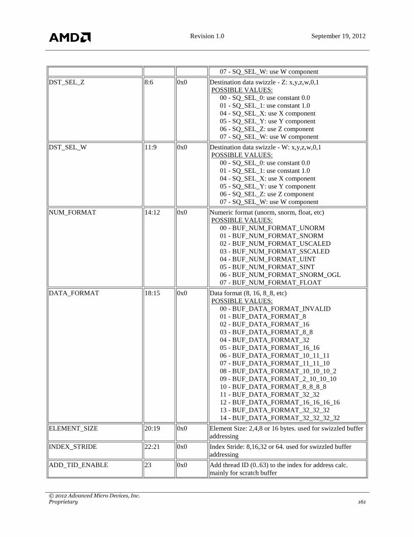
Revision 1.0 September 19, 2012
© 2012 Advanced Micro Devices, Inc. Proprietary 161
07 - SQ_SEL_W: use W component
DST_SEL_Z 8:6 0x0 Destination data swizzle - Z: x,y,z,w,0,1
POSSIBLE VALUES:
00 - SQ_SEL_0: use constant 0.0
01 - SQ_SEL_1: use constant 1.0
04 - SQ_SEL_X: use X component
05 - SQ_SEL_Y: use Y component
06 - SQ_SEL_Z: use Z component
07 - SQ_SEL_W: use W component
DST_SEL_W 11:9 0x0 Destination data swizzle - W: x,y,z,w,0,1
POSSIBLE VALUES:
00 - SQ_SEL_0: use constant 0.0
01 - SQ_SEL_1: use constant 1.0
04 - SQ_SEL_X: use X component
05 - SQ_SEL_Y: use Y component
06 - SQ_SEL_Z: use Z component
07 - SQ_SEL_W: use W component
NUM_FORMAT 14:12 0x0 Numeric format (unorm, snorm, float, etc)
POSSIBLE VALUES:
00 - BUF_NUM_FORMAT_UNORM
01 - BUF_NUM_FORMAT_SNORM
02 - BUF_NUM_FORMAT_USCALED
03 - BUF_NUM_FORMAT_SSCALED
04 - BUF_NUM_FORMAT_UINT
05 - BUF_NUM_FORMAT_SINT
06 - BUF_NUM_FORMAT_SNORM_OGL
07 - BUF_NUM_FORMAT_FLOAT
DATA_FORMAT 18:15 0x0 Data format (8, 16, 8_8, etc)
POSSIBLE VALUES:
00 - BUF_DATA_FORMAT_INVALID
01 - BUF_DATA_FORMAT_8
02 - BUF_DATA_FORMAT_16
03 - BUF_DATA_FORMAT_8_8
04 - BUF_DATA_FORMAT_32
05 - BUF_DATA_FORMAT_16_16
06 - BUF_DATA_FORMAT_10_11_11
07 - BUF_DATA_FORMAT_11_11_10
08 - BUF_DATA_FORMAT_10_10_10_2
09 - BUF_DATA_FORMAT_2_10_10_10
10 - BUF_DATA_FORMAT_8_8_8_8
11 - BUF_DATA_FORMAT_32_32
12 - BUF_DATA_FORMAT_16_16_16_16
13 - BUF_DATA_FORMAT_32_32_32
14 - BUF_DATA_FORMAT_32_32_32_32
ELEMENT_SIZE 20:19 0x0 Element Size: 2,4,8 or 16 bytes. used for swizzled buffer
addressing
INDEX_STRIDE 22:21 0x0 Index Stride: 8,16,32 or 64. used for swizzled buffer
addressing
ADD_TID_ENABLE 23 0x0 Add thread ID (0..63) to the index for address calc.
mainly for scratch buffer
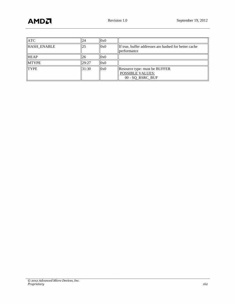
Revision 1.0 September 19, 2012
© 2012 Advanced Micro Devices, Inc. Proprietary 162
ATC 24 0x0
HASH_ENABLE 25 0x0 If true, buffer addresses are hashed for better cache
performance
HEAP 26 0x0
MTYPE 29:27 0x0
TYPE 31:30 0x0 Resource type: must be BUFFER
POSSIBLE VALUES:
00 - SQ_RSRC_BUF

Revision 1.0 September 19, 2012
© 2012 Advanced Micro Devices, Inc. Proprietary 163
6. Shader Image Resource Descriptor
SQ:SQ_IMG_RSRC_WORD0 · [R/W] · 32 bits · Access: 32 · GpuF0MMReg:0x8f10
DESCRIPTION: Image resource, word 0. This is not a real register, just a field description for constant data in
memory.
Field Name Bits Default Description
BASE_ADDRESS 31:0 0x0 Image base byte address, bits 39-8 (bits 7-0 are zero)
SQ:SQ_IMG_RSRC_WORD1 · [R/W] · 32 bits · Access: 32 · GpuF0MMReg:0x8f14
DESCRIPTION: Image resource, word 1. This is not a real register, just a field description for constant data in
memory.
Field Name Bits Default Description
BASE_ADDRESS_HI 7:0 0x0 Image base address, bits 47-40
MIN_LOD 19:8 0x0 Minimum LOD, 4.8 format
DATA_FORMAT 25:20 0x0 Data format (8, 8_8, 16, etc)
POSSIBLE VALUES:
00 - IMG_DATA_FORMAT_INVALID
01 - IMG_DATA_FORMAT_8
02 - IMG_DATA_FORMAT_16
03 - IMG_DATA_FORMAT_8_8
04 - IMG_DATA_FORMAT_32
05 - IMG_DATA_FORMAT_16_16
06 - IMG_DATA_FORMAT_10_11_11
07 - IMG_DATA_FORMAT_11_11_10
08 - IMG_DATA_FORMAT_10_10_10_2
09 - IMG_DATA_FORMAT_2_10_10_10
10 - IMG_DATA_FORMAT_8_8_8_8
11 - IMG_DATA_FORMAT_32_32
12 - IMG_DATA_FORMAT_16_16_16_16
13 - IMG_DATA_FORMAT_32_32_32
14 - IMG_DATA_FORMAT_32_32_32_32
16 - IMG_DATA_FORMAT_5_6_5
17 - IMG_DATA_FORMAT_1_5_5_5
18 - IMG_DATA_FORMAT_5_5_5_1
19 - IMG_DATA_FORMAT_4_4_4_4
20 - IMG_DATA_FORMAT_8_24
21 - IMG_DATA_FORMAT_24_8
22 - IMG_DATA_FORMAT_X24_8_32
32 - IMG_DATA_FORMAT_GB_GR
33 - IMG_DATA_FORMAT_BG_RG
34 - IMG_DATA_FORMAT_5_9_9_9
35 - Reserved
36 - Reserved
37 - Reserved
38 - Reserved
39 - Reserved
40 - Reserved
41 - Reserved

Revision 1.0 September 19, 2012
© 2012 Advanced Micro Devices, Inc. Proprietary 164
44 - IMG_DATA_FORMAT_FMASK8_S2_F1
45 - IMG_DATA_FORMAT_FMASK8_S4_F1
46 - IMG_DATA_FORMAT_FMASK8_S8_F1
47 - IMG_DATA_FORMAT_FMASK8_S2_F2
48 - IMG_DATA_FORMAT_FMASK8_S4_F2
49 - IMG_DATA_FORMAT_FMASK8_S4_F4
50 - IMG_DATA_FORMAT_FMASK16_S16_F1
51 - IMG_DATA_FORMAT_FMASK16_S8_F2
52 - IMG_DATA_FORMAT_FMASK32_S16_F2
53 - IMG_DATA_FORMAT_FMASK32_S8_F4
54 - IMG_DATA_FORMAT_FMASK32_S8_F8
55 - IMG_DATA_FORMAT_FMASK64_S16_F4
56 - IMG_DATA_FORMAT_FMASK64_S16_F8
57 - IMG_DATA_FORMAT_4_4
58 - IMG_DATA_FORMAT_6_5_5
59 - IMG_DATA_FORMAT_1
60 - IMG_DATA_FORMAT_1_REVERSED
61 - IMG_DATA_FORMAT_32_AS_8
62 - IMG_DATA_FORMAT_32_AS_8_8
63 - IMG_DATA_FORMAT_32_AS_32_32_32_32
NUM_FORMAT 29:26 0x0 Numeric format (unorm, snorm, float, etc)
POSSIBLE VALUES:
00 - IMG_NUM_FORMAT_UNORM
01 - IMG_NUM_FORMAT_SNORM
02 - IMG_NUM_FORMAT_USCALED
03 - IMG_NUM_FORMAT_SSCALED
04 - IMG_NUM_FORMAT_UINT
05 - IMG_NUM_FORMAT_SINT
06 - IMG_NUM_FORMAT_SNORM_OGL
07 - IMG_NUM_FORMAT_FLOAT
09 - IMG_NUM_FORMAT_SRGB
10 - IMG_NUM_FORMAT_UBNORM
11 - IMG_NUM_FORMAT_UBNORM_OGL
12 - IMG_NUM_FORMAT_UBINT
13 - IMG_NUM_FORMAT_UBSCALED
MTYPE 31:30 0x0
SQ:SQ_IMG_RSRC_WORD2 · [R/W] · 32 bits · Access: 32 · GpuF0MMReg:0x8f18
DESCRIPTION: Image resource, word 2. This is not a real register, just a field description for constant data in
memory.
Field Name Bits Default Description
WIDTH 13:0 0x0 Image width. Expressed as `width-1`, so 0 = width of 1.
HEIGHT 27:14 0x0 Image Height. Expressed as `height-1`, so 0 = height of
1.
PERF_MOD 30:28 0x0 Performance modulation
INTERLACED 31 0x0 Interlaced or not
SQ:SQ_IMG_RSRC_WORD3 · [R/W] · 32 bits · Access: 32 · GpuF0MMReg:0x8f1c
DESCRIPTION: Image resource, word 3. This is not a real register, just a field description for constant data in

Revision 1.0 September 19, 2012
© 2012 Advanced Micro Devices, Inc. Proprietary 165
memory.
Field Name Bits Default Description
DST_SEL_X 2:0 0x0 Destination data swizzle - X : x,y,z,w,0,1
POSSIBLE VALUES:
00 - SQ_SEL_0: use constant 0.0
01 - SQ_SEL_1: use constant 1.0
04 - SQ_SEL_X: use X component
05 - SQ_SEL_Y: use Y component
06 - SQ_SEL_Z: use Z component
07 - SQ_SEL_W: use W component
DST_SEL_Y 5:3 0x0 Destination data swizzle - X : x,y,z,w,0,1
POSSIBLE VALUES:
00 - SQ_SEL_0: use constant 0.0
01 - SQ_SEL_1: use constant 1.0
04 - SQ_SEL_X: use X component
05 - SQ_SEL_Y: use Y component
06 - SQ_SEL_Z: use Z component
07 - SQ_SEL_W: use W component
DST_SEL_Z 8:6 0x0 Destination data swizzle - X : x,y,z,w,0,1
POSSIBLE VALUES:
00 - SQ_SEL_0: use constant 0.0
01 - SQ_SEL_1: use constant 1.0
04 - SQ_SEL_X: use X component
05 - SQ_SEL_Y: use Y component
06 - SQ_SEL_Z: use Z component
07 - SQ_SEL_W: use W component
DST_SEL_W 11:9 0x0 Destination data swizzle - X : x,y,z,w,0,1
POSSIBLE VALUES:
00 - SQ_SEL_0: use constant 0.0
01 - SQ_SEL_1: use constant 1.0
04 - SQ_SEL_X: use X component
05 - SQ_SEL_Y: use Y component
06 - SQ_SEL_Z: use Z component
07 - SQ_SEL_W: use W component
BASE_LEVEL 15:12 0x0 Base level
LAST_LEVEL 19:16 0x0 Last level
TILING_INDEX 24:20 0x0 Tiling Index. Index into table of memory tiling options
(bank_width, bank_height, num_banks, tile_split,
macro_tile_aspect, micro_tile_aspect, array_mode).
POW2_PAD 25 0x0 memory footprint is padded to pwer-of-2 dimensions
MTYPE 26 0x0
ATC 27 0x0
TYPE 31:28 0x0 Resource type: 1d, 2d, 3d, cube, 1d_array, 2d_array,
2d_msaa, 2d_msaa_array.
POSSIBLE VALUES:
08 - SQ_RSRC_IMG_1D
09 - SQ_RSRC_IMG_2D
10 - SQ_RSRC_IMG_3D
11 - SQ_RSRC_IMG_CUBE

Revision 1.0 September 19, 2012
© 2012 Advanced Micro Devices, Inc. Proprietary 166
12 - SQ_RSRC_IMG_1D_ARRAY
13 - SQ_RSRC_IMG_2D_ARRAY
14 - SQ_RSRC_IMG_2D_MSAA
15 - SQ_RSRC_IMG_2D_MSAA_ARRAY
SQ:SQ_IMG_RSRC_WORD4 · [R/W] · 32 bits · Access: 32 · GpuF0MMReg:0x8f20
DESCRIPTION: Image resource, word 4. This is not a real register, just a field description for constant data in
memory.
Field Name Bits Default Description
DEPTH 12:0 0x0 Depth of 3d texture map. Units are `depth-1`, so 0 = 1
slice, 1=2slices.
PITCH 26:13 0x0 Pitch, in units of texels
SQ:SQ_IMG_RSRC_WORD5 · [R/W] · 32 bits · Access: 32 · GpuF0MMReg:0x8f24
DESCRIPTION: Image resource, word 5. This is not a real register, just a field description for constant data in
memory.
Field Name Bits Default Description
BASE_ARRAY 12:0 0x0 Absolute index of first valid array slice to use.
LAST_ARRAY 25:13 0x0 Absolute index of last valid array slice to use. For
cubemaps and cubemap arrays, LAST_ARRAY must be
programmed with BASE_ARRAY + (N*6) - 1, where N
is the number of cubemaps in the array, or N=1 for a
single cubemap.
SQ:SQ_IMG_RSRC_WORD6 · [R/W] · 32 bits · Access: 32 · GpuF0MMReg:0x8f28
DESCRIPTION: Image resource, word 6. This is not a real register, just a field description for constant data in
memory.
Field Name Bits Default Description
MIN_LOD_WARN 11:0 0x0 feedback trigger for LOD
COUNTER_BANK_ID 19:12 0x0
LOD_HDW_CNT_EN 20 0x0
SQ:SQ_IMG_RSRC_WORD7 · [R/W] · 32 bits · Access: 32 · GpuF0MMReg:0x8f2c
DESCRIPTION: Image resource, word 7. This is not a real register, just a field description for constant data in
memory.
Field Name Bits Default Description
UNUSED 31:0 0x0 unused. write zeros.

Revision 1.0 September 19, 2012
© 2012 Advanced Micro Devices, Inc. Proprietary 167
7. Shader Image Resource Sampler Descriptor
SQ:SQ_IMG_SAMP_WORD0 · [R/W] · 32 bits · Access: 32 · GpuF0MMReg:0x8f30
DESCRIPTION: Sampler word 0. This is not a real register, just a field description for constant data in memory.
Field Name Bits Default Description
CLAMP_X 2:0 0x0 clamp/wrap mode
POSSIBLE VALUES:
00 - SQ_TEX_WRAP
01 - SQ_TEX_MIRROR
02 - SQ_TEX_CLAMP_LAST_TEXEL: [0,1]
normalized, [0,dimen] unnormalized
03 - SQ_TEX_MIRROR_ONCE_LAST_TEXEL: [-
1,1]
04 - SQ_TEX_CLAMP_HALF_BORDER: [0,1]
normalized, [0,dimen] unnormalized
05 - SQ_TEX_MIRROR_ONCE_HALF_BORDER:
[-1,1]
06 - SQ_TEX_CLAMP_BORDER: [0,1] normalized,
[0,dimen] unnormalized
07 - SQ_TEX_MIRROR_ONCE_BORDER: [-1,1]
CLAMP_Y 5:3 0x0 clamp/wrap mode
POSSIBLE VALUES:
00 - SQ_TEX_WRAP
01 - SQ_TEX_MIRROR
02 - SQ_TEX_CLAMP_LAST_TEXEL: [0,1]
normalized, [0,dimen] unnormalized
03 - SQ_TEX_MIRROR_ONCE_LAST_TEXEL: [-
1,1]
04 - SQ_TEX_CLAMP_HALF_BORDER: [0,1]
normalized, [0,dimen] unnormalized
05 - SQ_TEX_MIRROR_ONCE_HALF_BORDER:
[-1,1]
06 - SQ_TEX_CLAMP_BORDER: [0,1] normalized,
[0,dimen] unnormalized
07 - SQ_TEX_MIRROR_ONCE_BORDER: [-1,1]
CLAMP_Z 8:6 0x0 clamp/wrap mode
POSSIBLE VALUES:
00 - SQ_TEX_WRAP
01 - SQ_TEX_MIRROR
02 - SQ_TEX_CLAMP_LAST_TEXEL: [0,1]
normalized, [0,dimen] unnormalized
03 - SQ_TEX_MIRROR_ONCE_LAST_TEXEL: [-
1,1]
04 - SQ_TEX_CLAMP_HALF_BORDER: [0,1]
normalized, [0,dimen] unnormalized
05 - SQ_TEX_MIRROR_ONCE_HALF_BORDER:
[-1,1]
06 - SQ_TEX_CLAMP_BORDER: [0,1] normalized,
[0,dimen] unnormalized

Revision 1.0 September 19, 2012
© 2012 Advanced Micro Devices, Inc. Proprietary 168
07 - SQ_TEX_MIRROR_ONCE_BORDER: [-1,1]
Reserved 11:9 0x0
DEPTH_COMPARE_FUNC 14:12 0x0 depth compare function
POSSIBLE VALUES:
00 - SQ_TEX_DEPTH_COMPARE_NEVER:
always 0
01 - SQ_TEX_DEPTH_COMPARE_LESS: 1 if
incoming Z < fetched data
02 - SQ_TEX_DEPTH_COMPARE_EQUAL: 1 if
incoming Z == fetched data
03 - SQ_TEX_DEPTH_COMPARE_LESSEQUAL:
1 if incoming Z <= fetched data
04 - SQ_TEX_DEPTH_COMPARE_GREATER: 1
if incoming Z > fetched data
05 - SQ_TEX_DEPTH_COMPARE_NOTEQUAL:
1 if incoming Z != fetched data
06 -
SQ_TEX_DEPTH_COMPARE_GREATEREQUAL: 1
if incoming Z >= fetched data
07 - SQ_TEX_DEPTH_COMPARE_ALWAYS:
always 1
FORCE_UNNORMALIZED 15 0x0 force address coords to be un-normalized
Reserved 18:16 0x0
MC_COORD_TRUNC 19 0x0
FORCE_DEGAMMA 20 0x0 force degamma on
Reserved 26:21 0x0
TRUNC_COORD 27 0x0 truncate coordinates
DISABLE_CUBE_WRAP 28 0x0 disable cubemap wrap
FILTER_MODE 30:29 0x0 filter mode; normal lerp, min or max filter
SQ:SQ_IMG_SAMP_WORD1 · [R/W] · 32 bits · Access: 32 · GpuF0MMReg:0x8f34
DESCRIPTION: Sampler word 1. This is not a real register, just a field description for constant data in memory.
Field Name Bits Default Description
MIN_LOD 11:0 0x0 minimum LOD: u4.8
MAX_LOD 23:12 0x0 maximum LOD: u4.8
PERF_MIP 27:24 0x0 perf mip
PERF_Z 31:28 0x0 perf z
SQ:SQ_IMG_SAMP_WORD2 · [R/W] · 32 bits · Access: 32 · GpuF0MMReg:0x8f38
DESCRIPTION: Sampler word 2. This is not a real register, just a field description for constant data in memory.
Field Name Bits Default Description
LOD_BIAS 13:0 0x0 LOD bias: S5.8
LOD_BIAS_SEC 19:14 0x0 LOD bias secondary: S1.4
XY_MAG_FILTER 21:20 0x0 magnification filter
POSSIBLE VALUES:

Revision 1.0 September 19, 2012
© 2012 Advanced Micro Devices, Inc. Proprietary 169
00 - SQ_TEX_XY_FILTER_POINT
01 - SQ_TEX_XY_FILTER_BILINEAR
02 - Reserved
03 - Reserved
XY_MIN_FILTER 23:22 0x0 minification filter
POSSIBLE VALUES:
00 - SQ_TEX_XY_FILTER_POINT
01 - SQ_TEX_XY_FILTER_BILINEAR
02 - Reserved
03 - Reserved
Z_FILTER 25:24 0x0 depth filter
POSSIBLE VALUES:
00 - SQ_TEX_Z_FILTER_NONE
01 - SQ_TEX_Z_FILTER_POINT
02 - SQ_TEX_Z_FILTER_LINEAR
MIP_FILTER 27:26 0x0 mip-level filter
POSSIBLE VALUES:
00 - SQ_TEX_Z_FILTER_NONE
01 - SQ_TEX_Z_FILTER_POINT
02 - SQ_TEX_Z_FILTER_LINEAR
MIP_POINT_PRECLAMP 28 0x0
DISABLE_LSB_CEIL 29 0x0
FILTER_PREC_FIX 30 0x0
SQ:SQ_IMG_SAMP_WORD3 · [R/W] · 32 bits · Access: 32 · GpuF0MMReg:0x8f3c
DESCRIPTION: Sampler word 3. This is not a real register, just a field description for constant data in memory.
Field Name Bits Default Description
BORDER_COLOR_PTR 11:0 0x0 pointer into a table of border colors
BORDER_COLOR_TYPE 31:30 0x0 Opaque-black, transparent-black, white or use border
color pointer.
POSSIBLE VALUES:
00 -
SQ_TEX_BORDER_COLOR_TRANS_BLACK: (0.0,
0.0, 0.0, 0.0)
01 -
SQ_TEX_BORDER_COLOR_OPAQUE_BLACK: (0.0,
0.0, 0.0, 1.0)
02 -
SQ_TEX_BORDER_COLOR_OPAQUE_WHITE: (1.0,
1.0, 1.0, 1.0)
03 - SQ_TEX_BORDER_COLOR_REGISTER: use
BORDER_COLOR_[XYZW]

Revision 1.0 September 19, 2012
© 2012 Advanced Micro Devices, Inc. Proprietary 170
8. Flat Scratch Descriptor
SQ:SQ_FLAT_SCRATCH_WORD0 · [R/W] · 32 bits · Access: 32 · GpuF0MMReg:0x8f40
Field Name Bits Default Description
SIZE 18:0 0x0
SQ:SQ_FLAT_SCRATCH_WORD1 · [R/W] · 32 bits · Access: 32 · GpuF0MMReg:0x8f44
Field Name Bits Default Description
OFFSET 23:0 0x0
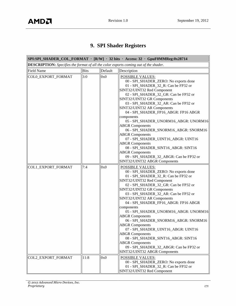
Revision 1.0 September 19, 2012
© 2012 Advanced Micro Devices, Inc. Proprietary 171
9. SPI Shader Registers
SPI:SPI_SHADER_COL_FORMAT · [R/W] · 32 bits · Access: 32 · GpuF0MMReg:0x28714
DESCRIPTION: Specifies the format of all the color exports coming out of the shader.
Field Name Bits Default Description
COL0_EXPORT_FORMAT 3:0 0x0 POSSIBLE VALUES:
00 - SPI_SHADER_ZERO: No exports done
01 - SPI_SHADER_32_R: Can be FP32 or
SINT32/UINT32 Red Component
02 - SPI_SHADER_32_GR: Can be FP32 or
SINT32/UINT32 GR Components
03 - SPI_SHADER_32_AR: Can be FP32 or
SINT32/UINT32 AR Components
04 - SPI_SHADER_FP16_ABGR: FP16 ABGR
components
05 - SPI_SHADER_UNORM16_ABGR: UNORM16
ABGR Components
06 - SPI_SHADER_SNORM16_ABGR: SNORM16
ABGR Components
07 - SPI_SHADER_UINT16_ABGR: UINT16
ABGR Components
08 - SPI_SHADER_SINT16_ABGR: SINT16
ABGR Components
09 - SPI_SHADER_32_ABGR: Can be FP32 or
SINT32/UINT32 ABGR Components
COL1_EXPORT_FORMAT 7:4 0x0 POSSIBLE VALUES:
00 - SPI_SHADER_ZERO: No exports done
01 - SPI_SHADER_32_R: Can be FP32 or
SINT32/UINT32 Red Component
02 - SPI_SHADER_32_GR: Can be FP32 or
SINT32/UINT32 GR Components
03 - SPI_SHADER_32_AR: Can be FP32 or
SINT32/UINT32 AR Components
04 - SPI_SHADER_FP16_ABGR: FP16 ABGR
components
05 - SPI_SHADER_UNORM16_ABGR: UNORM16
ABGR Components
06 - SPI_SHADER_SNORM16_ABGR: SNORM16
ABGR Components
07 - SPI_SHADER_UINT16_ABGR: UINT16
ABGR Components
08 - SPI_SHADER_SINT16_ABGR: SINT16
ABGR Components
09 - SPI_SHADER_32_ABGR: Can be FP32 or
SINT32/UINT32 ABGR Components
COL2_EXPORT_FORMAT 11:8 0x0 POSSIBLE VALUES:
00 - SPI_SHADER_ZERO: No exports done
01 - SPI_SHADER_32_R: Can be FP32 or
SINT32/UINT32 Red Component
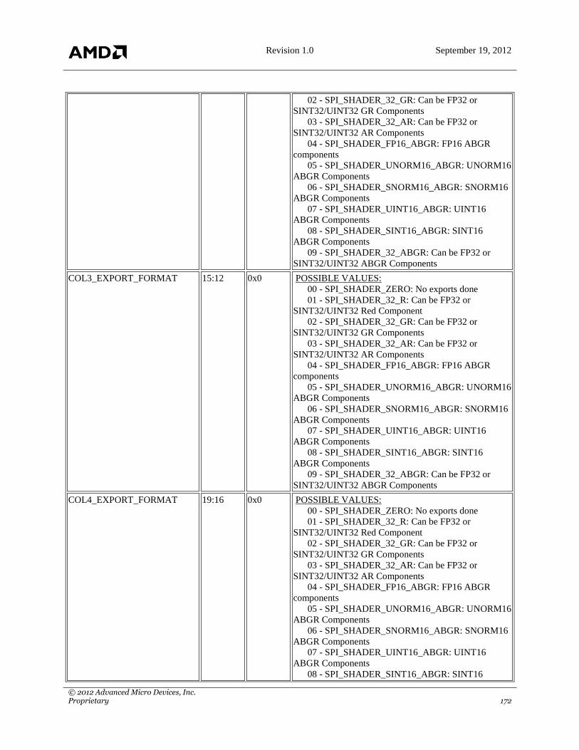
Revision 1.0 September 19, 2012
© 2012 Advanced Micro Devices, Inc. Proprietary 172
02 - SPI_SHADER_32_GR: Can be FP32 or
SINT32/UINT32 GR Components
03 - SPI_SHADER_32_AR: Can be FP32 or
SINT32/UINT32 AR Components
04 - SPI_SHADER_FP16_ABGR: FP16 ABGR
components
05 - SPI_SHADER_UNORM16_ABGR: UNORM16
ABGR Components
06 - SPI_SHADER_SNORM16_ABGR: SNORM16
ABGR Components
07 - SPI_SHADER_UINT16_ABGR: UINT16
ABGR Components
08 - SPI_SHADER_SINT16_ABGR: SINT16
ABGR Components
09 - SPI_SHADER_32_ABGR: Can be FP32 or
SINT32/UINT32 ABGR Components
COL3_EXPORT_FORMAT 15:12 0x0 POSSIBLE VALUES:
00 - SPI_SHADER_ZERO: No exports done
01 - SPI_SHADER_32_R: Can be FP32 or
SINT32/UINT32 Red Component
02 - SPI_SHADER_32_GR: Can be FP32 or
SINT32/UINT32 GR Components
03 - SPI_SHADER_32_AR: Can be FP32 or
SINT32/UINT32 AR Components
04 - SPI_SHADER_FP16_ABGR: FP16 ABGR
components
05 - SPI_SHADER_UNORM16_ABGR: UNORM16
ABGR Components
06 - SPI_SHADER_SNORM16_ABGR: SNORM16
ABGR Components
07 - SPI_SHADER_UINT16_ABGR: UINT16
ABGR Components
08 - SPI_SHADER_SINT16_ABGR: SINT16
ABGR Components
09 - SPI_SHADER_32_ABGR: Can be FP32 or
SINT32/UINT32 ABGR Components
COL4_EXPORT_FORMAT 19:16 0x0 POSSIBLE VALUES:
00 - SPI_SHADER_ZERO: No exports done
01 - SPI_SHADER_32_R: Can be FP32 or
SINT32/UINT32 Red Component
02 - SPI_SHADER_32_GR: Can be FP32 or
SINT32/UINT32 GR Components
03 - SPI_SHADER_32_AR: Can be FP32 or
SINT32/UINT32 AR Components
04 - SPI_SHADER_FP16_ABGR: FP16 ABGR
components
05 - SPI_SHADER_UNORM16_ABGR: UNORM16
ABGR Components
06 - SPI_SHADER_SNORM16_ABGR: SNORM16
ABGR Components
07 - SPI_SHADER_UINT16_ABGR: UINT16
ABGR Components
08 - SPI_SHADER_SINT16_ABGR: SINT16

Revision 1.0 September 19, 2012
© 2012 Advanced Micro Devices, Inc. Proprietary 173
ABGR Components
09 - SPI_SHADER_32_ABGR: Can be FP32 or
SINT32/UINT32 ABGR Components
COL5_EXPORT_FORMAT 23:20 0x0 POSSIBLE VALUES:
00 - SPI_SHADER_ZERO: No exports done
01 - SPI_SHADER_32_R: Can be FP32 or
SINT32/UINT32 Red Component
02 - SPI_SHADER_32_GR: Can be FP32 or
SINT32/UINT32 GR Components
03 - SPI_SHADER_32_AR: Can be FP32 or
SINT32/UINT32 AR Components
04 - SPI_SHADER_FP16_ABGR: FP16 ABGR
components
05 - SPI_SHADER_UNORM16_ABGR: UNORM16
ABGR Components
06 - SPI_SHADER_SNORM16_ABGR: SNORM16
ABGR Components
07 - SPI_SHADER_UINT16_ABGR: UINT16
ABGR Components
08 - SPI_SHADER_SINT16_ABGR: SINT16
ABGR Components
09 - SPI_SHADER_32_ABGR: Can be FP32 or
SINT32/UINT32 ABGR Components
COL6_EXPORT_FORMAT 27:24 0x0 POSSIBLE VALUES:
00 - SPI_SHADER_ZERO: No exports done
01 - SPI_SHADER_32_R: Can be FP32 or
SINT32/UINT32 Red Component
02 - SPI_SHADER_32_GR: Can be FP32 or
SINT32/UINT32 GR Components
03 - SPI_SHADER_32_AR: Can be FP32 or
SINT32/UINT32 AR Components
04 - SPI_SHADER_FP16_ABGR: FP16 ABGR
components
05 - SPI_SHADER_UNORM16_ABGR: UNORM16
ABGR Components
06 - SPI_SHADER_SNORM16_ABGR: SNORM16
ABGR Components
07 - SPI_SHADER_UINT16_ABGR: UINT16
ABGR Components
08 - SPI_SHADER_SINT16_ABGR: SINT16
ABGR Components
09 - SPI_SHADER_32_ABGR: Can be FP32 or
SINT32/UINT32 ABGR Components
COL7_EXPORT_FORMAT 31:28 0x0 POSSIBLE VALUES:
00 - SPI_SHADER_ZERO: No exports done
01 - SPI_SHADER_32_R: Can be FP32 or
SINT32/UINT32 Red Component
02 - SPI_SHADER_32_GR: Can be FP32 or
SINT32/UINT32 GR Components
03 - SPI_SHADER_32_AR: Can be FP32 or
SINT32/UINT32 AR Components
04 - SPI_SHADER_FP16_ABGR: FP16 ABGR

Revision 1.0 September 19, 2012
© 2012 Advanced Micro Devices, Inc. Proprietary 174
components
05 - SPI_SHADER_UNORM16_ABGR: UNORM16
ABGR Components
06 - SPI_SHADER_SNORM16_ABGR: SNORM16
ABGR Components
07 - SPI_SHADER_UINT16_ABGR: UINT16
ABGR Components
08 - SPI_SHADER_SINT16_ABGR: SINT16
ABGR Components
09 - SPI_SHADER_32_ABGR: Can be FP32 or
SINT32/UINT32 ABGR Components
SPI:SPI_SHADER_LATE_ALLOC_VS · [R/W] · 32 bits · Access: 32 · GpuF0MMReg:0xb11c
DESCRIPTION: Limits the number of VS that can be in flight without having param cache and position buffer
space
Field Name Bits Default Description
LIMIT 5:0 0x0 Max setting of 63, set to 1 to mimic VS pre-alloc
SPI:SPI_SHADER_PGM_HI_ES · [R/W] · 8 bits · Access: 8 · GpuF0MMReg:0xb324
DESCRIPTION: Shader base address
Field Name Bits Default Description
MEM_BASE 7:0 0x0
SPI:SPI_SHADER_PGM_HI_GS · [R/W] · 8 bits · Access: 8 · GpuF0MMReg:0xb224
DESCRIPTION: Shader base address
Field Name Bits Default Description
MEM_BASE 7:0 0x0
SPI:SPI_SHADER_PGM_HI_HS · [R/W] · 8 bits · Access: 8 · GpuF0MMReg:0xb424
DESCRIPTION: Shader base address
Field Name Bits Default Description
MEM_BASE 7:0 0x0
SPI:SPI_SHADER_PGM_HI_LS · [R/W] · 8 bits · Access: 8 · GpuF0MMReg:0xb524
DESCRIPTION: Shader base address
Field Name Bits Default Description
MEM_BASE 7:0 0x0
SPI:SPI_SHADER_PGM_HI_PS · [R/W] · 8 bits · Access: 8 · GpuF0MMReg:0xb024
DESCRIPTION: Shader base address
Field Name Bits Default Description
MEM_BASE 7:0 0x0

Revision 1.0 September 19, 2012
© 2012 Advanced Micro Devices, Inc. Proprietary 175
SPI:SPI_SHADER_PGM_HI_VS · [R/W] · 8 bits · Access: 8 · GpuF0MMReg:0xb124
DESCRIPTION: Shader base address
Field Name Bits Default Description
MEM_BASE 7:0 0x0
SPI:SPI_SHADER_PGM_LO_ES · [R/W] · 32 bits · Access: 32 · GpuF0MMReg:0xb320
DESCRIPTION: Shader base address
Field Name Bits Default Description
MEM_BASE 31:0 0x0
SPI:SPI_SHADER_PGM_LO_GS · [R/W] · 32 bits · Access: 32 · GpuF0MMReg:0xb220
DESCRIPTION: Shader base address
Field Name Bits Default Description
MEM_BASE 31:0 0x0
SPI:SPI_SHADER_PGM_LO_HS · [R/W] · 32 bits · Access: 32 · GpuF0MMReg:0xb420
DESCRIPTION: Shader base address
Field Name Bits Default Description
MEM_BASE 31:0 0x0
SPI:SPI_SHADER_PGM_LO_LS · [R/W] · 32 bits · Access: 32 · GpuF0MMReg:0xb520
DESCRIPTION: Shader base address
Field Name Bits Default Description
MEM_BASE 31:0 0x0
SPI:SPI_SHADER_PGM_LO_PS · [R/W] · 32 bits · Access: 32 · GpuF0MMReg:0xb020
DESCRIPTION: Shader base address
Field Name Bits Default Description
MEM_BASE 31:0 0x0
SPI:SPI_SHADER_PGM_LO_VS · [R/W] · 32 bits · Access: 32 · GpuF0MMReg:0xb120
DESCRIPTION: Shader base address
Field Name Bits Default Description
MEM_BASE 31:0 0x0
SPI:SPI_SHADER_PGM_RSRC1_ES · [R/W] · 32 bits · Access: 32 · GpuF0MMReg:0xb328
DESCRIPTION: Shader program settings for ES
Field Name Bits Default Description
VGPRS 5:0 0x0 Number of VGPRS, granularity 4. Range is from 0-63
allocating 4,8,12 ... 256

Revision 1.0 September 19, 2012
© 2012 Advanced Micro Devices, Inc. Proprietary 176
SGPRS 9:6 0x0 Number of SGPRS, granularity 8. Range is from 0-15
allocating 8,16,24 ... 128
PRIORITY 11:10 0x0 Drives spi_priority in spi_sq newWave cmd
FLOAT_MODE 19:12 0x0 Drives float_mode in spi_sq newWave cmd
PRIV 20 0x0 Drives priv in spi_sq newWave cmd
DX10_CLAMP 21 0x0 Drives dx10_clamp in spi_sq newWave cmd
DEBUG_MODE 22 0x0 Drives debug in spi_sq newWave cmd
IEEE_MODE 23 0x0 Drives ieee in spi_sq newWave cmd
VGPR_COMP_CNT 25:24 0x0 Tells SPI how many VGPR components to load
CU_GROUP_ENABLE 26 0x0 Set this bit to have ES prefer to send a wave to each
SIMD in a CU before moving to the next enabled CU.
When 0, ES prefers to send only one wave to each CU
before moving to the next enabled CU.
CACHE_CTL 29:27 0x0 Passed to SQ with each newwave
CDBG_USER 30 0x0 Passed to SQ with each newwave
SPI:SPI_SHADER_PGM_RSRC1_GS · [R/W] · 32 bits · Access: 32 · GpuF0MMReg:0xb228
DESCRIPTION: Shader program settings for GS
Field Name Bits Default Description
VGPRS 5:0 0x0 Number of VGPRS, granularity 4. Range is from 0-63
allocating 4,8,12 ... 256
SGPRS 9:6 0x0 Number of SGPRS, granularity 8. Range is from 0-15
allocating 8,16,24 ... 128
PRIORITY 11:10 0x0 Drives spi_priority in spi_sq newWave cmd
FLOAT_MODE 19:12 0x0 Drives float_mode in spi_sq newWave cmd
PRIV 20 0x0 Drives priv in spi_sq newWave cmd
DX10_CLAMP 21 0x0 Drives dx10_clamp in spi_sq newWave cmd
DEBUG_MODE 22 0x0 Drives debug in spi_sq newWave cmd
IEEE_MODE 23 0x0 Drives ieee in spi_sq newWave cmd
CU_GROUP_ENABLE 24 0x0 Set this bit to have GS prefer to send a wave to each
SIMD in a CU before moving to the next enabled CU.
When 0, GS prefers to send only one wave to each CU
before moving to the next enabled CU.
CACHE_CTL 27:25 0x0 Passed to SQ with each newwave
CDBG_USER 28 0x0 Passed to SQ with each newwave
SPI:SPI_SHADER_PGM_RSRC1_HS · [R/W] · 32 bits · Access: 32 · GpuF0MMReg:0xb428
DESCRIPTION: Shader program settings for HS
Field Name Bits Default Description
VGPRS 5:0 0x0 Number of VGPRS, granularity 4. Range is from 0-63
allocating 4,8,12 ... 256
SGPRS 9:6 0x0 Number of SGPRS, granularity 8. Range is from 0-15
allocating 8,16,24 ... 128

Revision 1.0 September 19, 2012
© 2012 Advanced Micro Devices, Inc. Proprietary 177
PRIORITY 11:10 0x0 Drives spi_priority in spi_sq newWave cmd
FLOAT_MODE 19:12 0x0 Drives float_mode in spi_sq newWave cmd
PRIV 20 0x0 Drives priv in spi_sq newWave cmd
DX10_CLAMP 21 0x0 Drives dx10_clamp in spi_sq newWave cmd
DEBUG_MODE 22 0x0 Drives debug in spi_sq newWave cmd
IEEE_MODE 23 0x0 Drives ieee in spi_sq newWave cmd
CACHE_CTL 26:24 0x0 Passed to SQ with each newwave
CDBG_USER 27 0x0 Passed to SQ with each newwave
SPI:SPI_SHADER_PGM_RSRC1_LS · [R/W] · 32 bits · Access: 32 · GpuF0MMReg:0xb528
DESCRIPTION: Shader program settings for LS
Field Name Bits Default Description
VGPRS 5:0 0x0 Number of VGPRS, granularity 4. Range is from 0-63
allocating 4,8,12 ... 256
SGPRS 9:6 0x0 Number of SGPRS, granularity 8. Range is from 0-15
allocating 8,16,24 ... 128
PRIORITY 11:10 0x0 Drives spi_priority in spi_sq newWave cmd
FLOAT_MODE 19:12 0x0 Drives float_mode in spi_sq newWave cmd
PRIV 20 0x0 Drives priv in spi_sq newWave cmd
DX10_CLAMP 21 0x0 Drives dx10_clamp in spi_sq newWave cmd
DEBUG_MODE 22 0x0 Drives debug in spi_sq newWave cmd
IEEE_MODE 23 0x0 Drives ieee in spi_sq newWave cmd
VGPR_COMP_CNT 25:24 0x0 Tells SPI how many VGPR components to load
CACHE_CTL 28:26 0x0 Passed to SQ with each newwave
CDBG_USER 29 0x0 Passed to SQ with each newwave
SPI:SPI_SHADER_PGM_RSRC1_PS · [R/W] · 32 bits · Access: 32 · GpuF0MMReg:0xb028
DESCRIPTION: Shader program settings for PS
Field Name Bits Default Description
VGPRS 5:0 0x0 Number of VGPRS, granularity 4. Range is from 0-63
allocating 4,8,12 ... 256
SGPRS 9:6 0x0 Number of SGPRS, granularity 8. Range is from 0-15
allocating 8,16,24 ... 128
PRIORITY 11:10 0x0 Drives spi_priority in spi_sq newWave cmd
FLOAT_MODE 19:12 0x0 Drives float_mode in spi_sq newWave cmd
PRIV 20 0x0 Drives priv in spi_sq newWave cmd
DX10_CLAMP 21 0x0 Drives dx10_clamp in spi_sq newWave cmd
DEBUG_MODE 22 0x0 Drives debug in spi_sq newWave cmd
IEEE_MODE 23 0x0 Drives ieee in spi_sq newWave cmd
CU_GROUP_DISABLE 24 0x0 Set this bit to have PS prefer to send only one wave to
each CU before moving to the next enabled CU. When 0,

Revision 1.0 September 19, 2012
© 2012 Advanced Micro Devices, Inc. Proprietary 178
PS prefers to send a wave to each SIMD in a CU before
moving to the next enabled CU.
CACHE_CTL 27:25 0x0 Passed to SQ with each newwave
CDBG_USER 28 0x0 Passed to SQ with each newwave
SPI:SPI_SHADER_PGM_RSRC1_VS · [R/W] · 32 bits · Access: 32 · GpuF0MMReg:0xb128
DESCRIPTION: Shader program settings for VS
Field Name Bits Default Description
VGPRS 5:0 0x0 Number of VGPRS, granularity 4. Range is from 0-63
allocating 4,8,12 ... 256
SGPRS 9:6 0x0 Number of SGPRS, granularity 8. Range is from 0-15
allocating 8,16,24 ... 128
PRIORITY 11:10 0x0 Drives spi_priority in spi_sq newWave cmd
FLOAT_MODE 19:12 0x0 Drives float_mode in spi_sq newWave cmd
PRIV 20 0x0 Drives priv in spi_sq newWave cmd
DX10_CLAMP 21 0x0 Drives dx10_clamp in spi_sq newWave cmd
DEBUG_MODE 22 0x0 Drives debug in spi_sq newWave cmd
IEEE_MODE 23 0x0 Drives ieee in spi_sq newWave cmd
VGPR_COMP_CNT 25:24 0x0 Tells SPI how many VGPR components to load
CU_GROUP_ENABLE 26 0x0 Set this bit to have VS prefer to send a wave to each
SIMD in a CU before moving to the next enabled CU.
When 0, VS prefers to send only one wave to each CU
before moving to the next enabled CU.
CACHE_CTL 29:27 0x0 Passed to SQ with each newwave
CDBG_USER 30 0x0 Passed to SQ with each newwave
SPI:SPI_SHADER_PGM_RSRC2_ES · [R/W] · 32 bits · Access: 32 · GpuF0MMReg:0xb32c
DESCRIPTION: Shader program settings for ES
Field Name Bits Default Description
SCRATCH_EN 0 0x0 This wave uses scratch space for register spilling
USER_SGPR 5:1 0x0 Number of USER_DATA terms that should be initialized
by SPI. Range is 0-16.
TRAP_PRESENT 6 0x0 Enables trap processing. Sets trap_en bit to SQ and
causes SPI to alloc 16 extra SGPR and write TBA/TMA
values to SGPR.
OC_LDS_EN 7 0x0 Enables loading of offchip related info to SGPR. See
shader pgm guide for details
EXCP_EN 16:8 0x0 Drives excp bits in spi_sq newWave cmd
LDS_SIZE 28:20 0x0 Amount of LDS space to alloc for each onchip-GS
subgroup, and should only be >0 if doing onchip-GS.
Granularity 128, range is 0 to 128 which allocates 0 to
16K dwords.

Revision 1.0 September 19, 2012
© 2012 Advanced Micro Devices, Inc. Proprietary 179
SPI:SPI_SHADER_PGM_RSRC2_GS · [R/W] · 32 bits · Access: 32 · GpuF0MMReg:0xb22c
DESCRIPTION: Shader program settings for GS
Field Name Bits Default Description
SCRATCH_EN 0 0x0 This wave uses scratch space for register spilling
USER_SGPR 5:1 0x0 Number of USER_DATA terms that should be initialized
by SPI. Range is 0-16.
TRAP_PRESENT 6 0x0 Enables trap processing. Sets trap_en bit to SQ and
causes SPI to alloc 16 extra SGPR and write TBA/TMA
values to SGPR.
EXCP_EN 15:7 0x0 Drives excp bits in spi_sq newWave cmd
SPI:SPI_SHADER_PGM_RSRC2_HS · [R/W] · 32 bits · Access: 32 · GpuF0MMReg:0xb42c
DESCRIPTION: Shader program settings for HS
Field Name Bits Default Description
SCRATCH_EN 0 0x0 This wave uses scratch space for register spilling
USER_SGPR 5:1 0x0 Number of USER_DATA terms that should be initialized
by SPI. Range is 0-16.
TRAP_PRESENT 6 0x0 Enables trap processing. Sets trap_en bit to SQ and
causes SPI to alloc 16 extra SGPR and write TBA/TMA
values to SGPR.
OC_LDS_EN 7 0x0 Enables loading of offchip related info to SGPR. See
shader pgm guide for details
TG_SIZE_EN 8 0x0 Enables loading of threadgroup related info to SGPR.
See shader pgm guide for details
EXCP_EN 17:9 0x0 Drives excp bits in spi_sq newWave cmd
SPI:SPI_SHADER_PGM_RSRC2_LS · [R/W] · 32 bits · Access: 32 · GpuF0MMReg:0xb52c
DESCRIPTION: Shader program settings for LS
Field Name Bits Default Description
SCRATCH_EN 0 0x0 This wave uses scratch space for register spilling
USER_SGPR 5:1 0x0 Number of USER_DATA terms that should be initialized
by SPI. Range is 0-16.
TRAP_PRESENT 6 0x0 Enables trap processing. Sets trap_en bit to SQ and
causes SPI to alloc 16 extra SGPR and write TBA/TMA
values to SGPR.
LDS_SIZE 15:7 0x0 Amount of LDS space to alloc for each threadgroup.
Granularity 128, range is 0 to 128 which allocates 0 to
16K dwords.
EXCP_EN 24:16 0x0 Drives excp bits in spi_sq newWave cmd
SPI:SPI_SHADER_PGM_RSRC2_PS · [R/W] · 32 bits · Access: 32 · GpuF0MMReg:0xb02c
DESCRIPTION: Shader program settings for PS
Field Name Bits Default Description
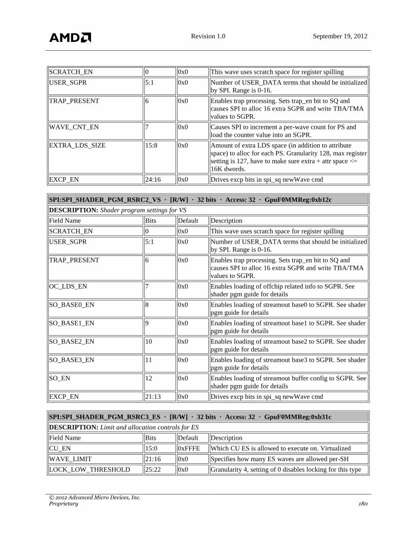
Revision 1.0 September 19, 2012
© 2012 Advanced Micro Devices, Inc. Proprietary 180
SCRATCH_EN 0 0x0 This wave uses scratch space for register spilling
USER_SGPR 5:1 0x0 Number of USER_DATA terms that should be initialized
by SPI. Range is 0-16.
TRAP_PRESENT 6 0x0 Enables trap processing. Sets trap_en bit to SQ and
causes SPI to alloc 16 extra SGPR and write TBA/TMA
values to SGPR.
WAVE_CNT_EN 7 0x0 Causes SPI to increment a per-wave count for PS and
load the counter value into an SGPR.
EXTRA_LDS_SIZE 15:8 0x0 Amount of extra LDS space (in addition to attribute
space) to alloc for each PS. Granularity 128, max register
setting is 127, have to make sure extra + attr space <=
16K dwords.
EXCP_EN 24:16 0x0 Drives excp bits in spi_sq newWave cmd
SPI:SPI_SHADER_PGM_RSRC2_VS · [R/W] · 32 bits · Access: 32 · GpuF0MMReg:0xb12c
DESCRIPTION: Shader program settings for VS
Field Name Bits Default Description
SCRATCH_EN 0 0x0 This wave uses scratch space for register spilling
USER_SGPR 5:1 0x0 Number of USER_DATA terms that should be initialized
by SPI. Range is 0-16.
TRAP_PRESENT 6 0x0 Enables trap processing. Sets trap_en bit to SQ and
causes SPI to alloc 16 extra SGPR and write TBA/TMA
values to SGPR.
OC_LDS_EN 7 0x0 Enables loading of offchip related info to SGPR. See
shader pgm guide for details
SO_BASE0_EN 8 0x0 Enables loading of streamout base0 to SGPR. See shader
pgm guide for details
SO_BASE1_EN 9 0x0 Enables loading of streamout base1 to SGPR. See shader
pgm guide for details
SO_BASE2_EN 10 0x0 Enables loading of streamout base2 to SGPR. See shader
pgm guide for details
SO_BASE3_EN 11 0x0 Enables loading of streamout base3 to SGPR. See shader
pgm guide for details
SO_EN 12 0x0 Enables loading of streamout buffer config to SGPR. See
shader pgm guide for details
EXCP_EN 21:13 0x0 Drives excp bits in spi_sq newWave cmd
SPI:SPI_SHADER_PGM_RSRC3_ES · [R/W] · 32 bits · Access: 32 · GpuF0MMReg:0xb31c
DESCRIPTION: Limit and allocation controls for ES
Field Name Bits Default Description
CU_EN 15:0 0xFFFE Which CU ES is allowed to execute on. Virtualized
WAVE_LIMIT 21:16 0x0 Specifies how many ES waves are allowed per-SH
LOCK_LOW_THRESHOLD 25:22 0x0 Granularity 4, setting of 0 disables locking for this type

Revision 1.0 September 19, 2012
© 2012 Advanced Micro Devices, Inc. Proprietary 181
SPI:SPI_SHADER_PGM_RSRC3_GS · [R/W] · 32 bits · Access: 32 · GpuF0MMReg:0xb21c
DESCRIPTION: Limit and allocation controls for GS
Field Name Bits Default Description
CU_EN 15:0 0xFFFF Which CU GS is allowed to execute on. Virtualized
WAVE_LIMIT 21:16 0x0 Specifies how many GS waves are allowed per-SH
LOCK_LOW_THRESHOLD 25:22 0x0 Granularity 4, setting of 0 disables locking for this type
SPI:SPI_SHADER_PGM_RSRC3_HS · [R/W] · 32 bits · Access: 32 · GpuF0MMReg:0xb41c
DESCRIPTION: Limit and allocation controls for HS
Field Name Bits Default Description
WAVE_LIMIT 5:0 0x0 Specifies how many HS waves are allowed per-SH
LOCK_LOW_THRESHOLD 9:6 0x0 Granularity 4, setting of 0 disables locking for this type
SPI:SPI_SHADER_PGM_RSRC3_LS · [R/W] · 32 bits · Access: 32 · GpuF0MMReg:0xb51c
DESCRIPTION: Limit and allocation controls for LS
Field Name Bits Default Description
CU_EN 15:0 0xFFFC Which CU LS is allowed to execute on. Virtualized
WAVE_LIMIT 21:16 0x0 Specifies how many LS waves are allowed per-SH
LOCK_LOW_THRESHOLD 25:22 0x0 Granularity 4, setting of 0 disables locking for this type
SPI:SPI_SHADER_PGM_RSRC3_PS · [R/W] · 32 bits · Access: 32 · GpuF0MMReg:0xb01c
DESCRIPTION: Limit and allocation controls for PS
Field Name Bits Default Description
CU_EN 15:0 0xFFFF Which CU PS is allowed to execute on. Virtualized
WAVE_LIMIT 21:16 0x0 Specifies how many PS waves are allowed per-SH
LOCK_LOW_THRESHOLD 25:22 0x0 Granularity 4, setting of 0 disables locking for this type
SPI:SPI_SHADER_PGM_RSRC3_VS · [R/W] · 32 bits · Access: 32 · GpuF0MMReg:0xb118
DESCRIPTION: Limit and allocation controls for VS
Field Name Bits Default Description
CU_EN 15:0 0xFFFF Which CU VS is allowed to execute on. Virtualized
WAVE_LIMIT 21:16 0x0 Specifies how many VS waves are allowed per-SH
LOCK_LOW_THRESHOLD 25:22 0x0 Granularity 4, setting of 0 disables locking for this type
SPI:SPI_SHADER_POS_FORMAT · [R/W] · 32 bits · Access: 32 · GpuF0MMReg:0x2870c
DESCRIPTION: Specifies the format of the position exports coming out of the shader.
Field Name Bits Default Description
POS0_EXPORT_FORMAT 3:0 0x0 POSSIBLE VALUES:
00 - SPI_SHADER_NONE: SPI_SHADER_NONE
01 - SPI_SHADER_1COMP:
SPI_SHADER_1COMP
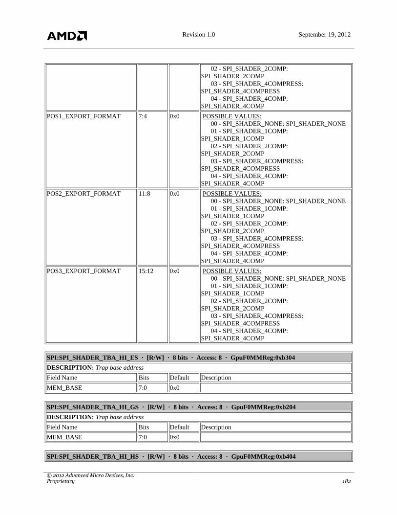
Revision 1.0 September 19, 2012
© 2012 Advanced Micro Devices, Inc. Proprietary 182
02 - SPI_SHADER_2COMP:
SPI_SHADER_2COMP
03 - SPI_SHADER_4COMPRESS:
SPI_SHADER_4COMPRESS
04 - SPI_SHADER_4COMP:
SPI_SHADER_4COMP
POS1_EXPORT_FORMAT 7:4 0x0 POSSIBLE VALUES:
00 - SPI_SHADER_NONE: SPI_SHADER_NONE
01 - SPI_SHADER_1COMP:
SPI_SHADER_1COMP
02 - SPI_SHADER_2COMP:
SPI_SHADER_2COMP
03 - SPI_SHADER_4COMPRESS:
SPI_SHADER_4COMPRESS
04 - SPI_SHADER_4COMP:
SPI_SHADER_4COMP
POS2_EXPORT_FORMAT 11:8 0x0 POSSIBLE VALUES:
00 - SPI_SHADER_NONE: SPI_SHADER_NONE
01 - SPI_SHADER_1COMP:
SPI_SHADER_1COMP
02 - SPI_SHADER_2COMP:
SPI_SHADER_2COMP
03 - SPI_SHADER_4COMPRESS:
SPI_SHADER_4COMPRESS
04 - SPI_SHADER_4COMP:
SPI_SHADER_4COMP
POS3_EXPORT_FORMAT 15:12 0x0 POSSIBLE VALUES:
00 - SPI_SHADER_NONE: SPI_SHADER_NONE
01 - SPI_SHADER_1COMP:
SPI_SHADER_1COMP
02 - SPI_SHADER_2COMP:
SPI_SHADER_2COMP
03 - SPI_SHADER_4COMPRESS:
SPI_SHADER_4COMPRESS
04 - SPI_SHADER_4COMP:
SPI_SHADER_4COMP
SPI:SPI_SHADER_TBA_HI_ES · [R/W] · 8 bits · Access: 8 · GpuF0MMReg:0xb304
DESCRIPTION: Trap base address
Field Name Bits Default Description
MEM_BASE 7:0 0x0
SPI:SPI_SHADER_TBA_HI_GS · [R/W] · 8 bits · Access: 8 · GpuF0MMReg:0xb204
DESCRIPTION: Trap base address
Field Name Bits Default Description
MEM_BASE 7:0 0x0
SPI:SPI_SHADER_TBA_HI_HS · [R/W] · 8 bits · Access: 8 · GpuF0MMReg:0xb404
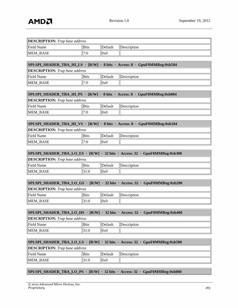
Revision 1.0 September 19, 2012
© 2012 Advanced Micro Devices, Inc. Proprietary 183
DESCRIPTION: Trap base address
Field Name Bits Default Description
MEM_BASE 7:0 0x0
SPI:SPI_SHADER_TBA_HI_LS · [R/W] · 8 bits · Access: 8 · GpuF0MMReg:0xb504
DESCRIPTION: Trap base address
Field Name Bits Default Description
MEM_BASE 7:0 0x0
SPI:SPI_SHADER_TBA_HI_PS · [R/W] · 8 bits · Access: 8 · GpuF0MMReg:0xb004
DESCRIPTION: Trap base address
Field Name Bits Default Description
MEM_BASE 7:0 0x0
SPI:SPI_SHADER_TBA_HI_VS · [R/W] · 8 bits · Access: 8 · GpuF0MMReg:0xb104
DESCRIPTION: Trap base address
Field Name Bits Default Description
MEM_BASE 7:0 0x0
SPI:SPI_SHADER_TBA_LO_ES · [R/W] · 32 bits · Access: 32 · GpuF0MMReg:0xb300
DESCRIPTION: Trap base address
Field Name Bits Default Description
MEM_BASE 31:0 0x0
SPI:SPI_SHADER_TBA_LO_GS · [R/W] · 32 bits · Access: 32 · GpuF0MMReg:0xb200
DESCRIPTION: Trap base address
Field Name Bits Default Description
MEM_BASE 31:0 0x0
SPI:SPI_SHADER_TBA_LO_HS · [R/W] · 32 bits · Access: 32 · GpuF0MMReg:0xb400
DESCRIPTION: Trap base address
Field Name Bits Default Description
MEM_BASE 31:0 0x0
SPI:SPI_SHADER_TBA_LO_LS · [R/W] · 32 bits · Access: 32 · GpuF0MMReg:0xb500
DESCRIPTION: Trap base address
Field Name Bits Default Description
MEM_BASE 31:0 0x0
SPI:SPI_SHADER_TBA_LO_PS · [R/W] · 32 bits · Access: 32 · GpuF0MMReg:0xb000

Revision 1.0 September 19, 2012
© 2012 Advanced Micro Devices, Inc. Proprietary 184
DESCRIPTION: Trap base address
Field Name Bits Default Description
MEM_BASE 31:0 0x0
SPI:SPI_SHADER_TBA_LO_VS · [R/W] · 32 bits · Access: 32 · GpuF0MMReg:0xb100
DESCRIPTION: Trap base address
Field Name Bits Default Description
MEM_BASE 31:0 0x0
SPI:SPI_SHADER_TMA_HI_ES · [R/W] · 8 bits · Access: 8 · GpuF0MMReg:0xb30c
DESCRIPTION: Trap mem address
Field Name Bits Default Description
MEM_BASE 7:0 0x0
SPI:SPI_SHADER_TMA_HI_GS · [R/W] · 8 bits · Access: 8 · GpuF0MMReg:0xb20c
DESCRIPTION: Trap mem address
Field Name Bits Default Description
MEM_BASE 7:0 0x0
SPI:SPI_SHADER_TMA_HI_HS · [R/W] · 8 bits · Access: 8 · GpuF0MMReg:0xb40c
DESCRIPTION: Trap mem address
Field Name Bits Default Description
MEM_BASE 7:0 0x0
SPI:SPI_SHADER_TMA_HI_LS · [R/W] · 8 bits · Access: 8 · GpuF0MMReg:0xb50c
DESCRIPTION: Trap mem address
Field Name Bits Default Description
MEM_BASE 7:0 0x0
SPI:SPI_SHADER_TMA_HI_PS · [R/W] · 8 bits · Access: 8 · GpuF0MMReg:0xb00c
DESCRIPTION: Trap mem address
Field Name Bits Default Description
MEM_BASE 7:0 0x0
SPI:SPI_SHADER_TMA_HI_VS · [R/W] · 8 bits · Access: 8 · GpuF0MMReg:0xb10c
DESCRIPTION: Trap mem address
Field Name Bits Default Description
MEM_BASE 7:0 0x0
SPI:SPI_SHADER_TMA_LO_ES · [R/W] · 32 bits · Access: 32 · GpuF0MMReg:0xb308

Revision 1.0 September 19, 2012
© 2012 Advanced Micro Devices, Inc. Proprietary 185
DESCRIPTION: Trap mem address
Field Name Bits Default Description
MEM_BASE 31:0 0x0
SPI:SPI_SHADER_TMA_LO_GS · [R/W] · 32 bits · Access: 32 · GpuF0MMReg:0xb208
DESCRIPTION: Trap mem address
Field Name Bits Default Description
MEM_BASE 31:0 0x0
SPI:SPI_SHADER_TMA_LO_HS · [R/W] · 32 bits · Access: 32 · GpuF0MMReg:0xb408
DESCRIPTION: Trap mem address
Field Name Bits Default Description
MEM_BASE 31:0 0x0
SPI:SPI_SHADER_TMA_LO_LS · [R/W] · 32 bits · Access: 32 · GpuF0MMReg:0xb508
DESCRIPTION: Trap mem address
Field Name Bits Default Description
MEM_BASE 31:0 0x0
SPI:SPI_SHADER_TMA_LO_PS · [R/W] · 32 bits · Access: 32 · GpuF0MMReg:0xb008
DESCRIPTION: Trap mem address
Field Name Bits Default Description
MEM_BASE 31:0 0x0
SPI:SPI_SHADER_TMA_LO_VS · [R/W] · 32 bits · Access: 32 · GpuF0MMReg:0xb108
DESCRIPTION: Trap mem address
Field Name Bits Default Description
MEM_BASE 31:0 0x0
SPI:SPI_SHADER_USER_DATA_ES_[0-15] · [R/W] · 32 bits · Access: 32 · GpuF0MMReg:0xb330-
0xb36c
DESCRIPTION: Persistent USER_DATA terms that can be written to SGPR with each ES wave.
Field Name Bits Default Description
DATA 31:0 0x0
SPI:SPI_SHADER_USER_DATA_GS_[0-15] · [R/W] · 32 bits · Access: 32 · GpuF0MMReg:0xb230-
0xb26c
DESCRIPTION: Persistent USER_DATA terms that can be written to SGPR with each GS wave.
Field Name Bits Default Description
DATA 31:0 0x0

Revision 1.0 September 19, 2012
© 2012 Advanced Micro Devices, Inc. Proprietary 186
SPI:SPI_SHADER_USER_DATA_HS_[0-15] · [R/W] · 32 bits · Access: 32 · GpuF0MMReg:0xb430-
0xb46c
DESCRIPTION: Persistent USER_DATA terms that can be written to SGPR with each HS wave.
Field Name Bits Default Description
DATA 31:0 0x0
SPI:SPI_SHADER_USER_DATA_LS_[0-15] · [R/W] · 32 bits · Access: 32 · GpuF0MMReg:0xb530-
0xb56c
DESCRIPTION: Persistent USER_DATA terms that can be written to SGPR with each LS wave.
Field Name Bits Default Description
DATA 31:0 0x0
SPI:SPI_SHADER_USER_DATA_PS_[0-15] · [R/W] · 32 bits · Access: 32 · GpuF0MMReg:0xb030-
0xb06c
DESCRIPTION: Persistent USER_DATA terms that can be written to SGPR with each PS wave.
Field Name Bits Default Description
DATA 31:0 0x0
SPI:SPI_SHADER_USER_DATA_VS_[0-15] · [R/W] · 32 bits · Access: 32 · GpuF0MMReg:0xb130-
0xb16c
DESCRIPTION: Persistent USER_DATA terms that can be written to SGPR with each VS wave.
Field Name Bits Default Description
DATA 31:0 0x0
SPI:SPI_SHADER_Z_FORMAT · [R/W] · 32 bits · Access: 32 · GpuF0MMReg:0x28710
DESCRIPTION: Specifies the format of the Z export coming out of the shader.
Field Name Bits Default Description
Z_EXPORT_FORMAT 3:0 0x0 POSSIBLE VALUES:
00 - SPI_SHADER_ZERO: No exports done
01 - SPI_SHADER_32_R: Can be FP32 or
SINT32/UINT32 Red Component
02 - SPI_SHADER_32_GR: Can be FP32 or
SINT32/UINT32 GR Components
03 - SPI_SHADER_32_AR: Can be FP32 or
SINT32/UINT32 AR Components
04 - SPI_SHADER_FP16_ABGR: FP16 ABGR
components
05 - SPI_SHADER_UNORM16_ABGR: UNORM16
ABGR Components
06 - SPI_SHADER_SNORM16_ABGR: SNORM16
ABGR Components
07 - SPI_SHADER_UINT16_ABGR: UINT16
ABGR Components
08 - SPI_SHADER_SINT16_ABGR: SINT16
ABGR Components
09 - SPI_SHADER_32_ABGR: Can be FP32 or

Revision 1.0 September 19, 2012
© 2012 Advanced Micro Devices, Inc. Proprietary 187
SINT32/UINT32 ABGR Components

Revision 1.0 September 19, 2012
© 2012 Advanced Micro Devices, Inc. Proprietary 188
10. SPI Registers
SPI:SPI_ARB_CYCLES_0 · [R/W] · 32 bits · Access: 32 · GpuF0MMReg:0xc704
DESCRIPTION: Granularity is 16 clocks. Allows 16ns to 1ms at 1GHZ clock. Should be written broadcast, stored
per SE.
Field Name Bits Default Description
TS0_DURATION 15:0 0x0 Duration for Timeslice 0.
TS1_DURATION 31:16 0x0 Duration for Timeslice 1.
SPI:SPI_ARB_CYCLES_1 · [R/W] · 32 bits · Access: 32 · GpuF0MMReg:0xc708
DESCRIPTION: Granularity is 16 clocks. Allows 16ns to 1ms at 1GHZ clock. Should be written broadcast, stored
per SE.
Field Name Bits Default Description
TS2_DURATION 15:0 0x0 Duration for Timeslice 2.
TS3_DURATION 31:16 0x0 Duration for Timeslice 3.
SPI:SPI_ARB_PRIORITY · [R/W] · 32 bits · Access: 32 · GpuF0MMReg:0xc700
DESCRIPTION: Pipe prioirty during each timeslice duration. Should be written broadcast, stored per SE.
Field Name Bits Default Description
PIPE_ORDER_TS0 2:0 0x0 Pipe priority order setting during timeslice0
POSSIBLE VALUES:
00 - CS_H, HP3D, CS_M, GFX, CS_L
01 - HP3D, CS_H, CS_M, GFX, CS_L
02 - HP3D, CS_H, GFX, CS_M, CS_L
03 - HP3D, GFX, CS_H, CS_M, CS_L
04 - CS_H, CS_M, CS_L, HP3D, GFX
05 - CS_M, CS_L, HP3D, GFX, CS_H
06 - CS_L, HP3D, GFX, CS_H, CS_M
PIPE_ORDER_TS1 5:3 0x0 Pipe priority order setting during timeslice1
PIPE_ORDER_TS2 8:6 0x0 Pipe priority order setting during timeslice2
PIPE_ORDER_TS3 11:9 0x0 Pipe priority order setting during timeslice3
TS0_DUR_MULT 13:12 0x0 Number of sclks used to increment duration count: 0-16,
1-64, 2-128, 3-256
TS1_DUR_MULT 15:14 0x0 Number of sclks used to increment duration count: 0-16,
1-64, 2-128, 3-256
TS2_DUR_MULT 17:16 0x0 Number of sclks used to increment duration count: 0-16,
1-64, 2-128, 3-256
TS3_DUR_MULT 19:18 0x0 Number of sclks used to increment duration count: 0-16,
1-64, 2-128, 3-256
SPI:SPI_BARYC_CNTL · [R/W] · 32 bits · Access: 32 · GpuF0MMReg:0x286e0
DESCRIPTION: Barycentric interpolation control in BCI
Field Name Bits Default Description

Revision 1.0 September 19, 2012
© 2012 Advanced Micro Devices, Inc. Proprietary 189
PERSP_CENTER_CNTL 0 0x0 POSSIBLE VALUES:
00 - On at center
01 - On at centroid
PERSP_CENTROID_CNTL 4 0x0 POSSIBLE VALUES:
00 - On at centroid
01 - On at center
LINEAR_CENTER_CNTL 8 0x0 POSSIBLE VALUES:
00 - On at center
01 - On at centroid
LINEAR_CENTROID_CNTL 12 0x0 POSSIBLE VALUES:
00 - On at centroid
01 - On at center
POS_FLOAT_LOCATION 17:16 0x0 POSSIBLE VALUES:
00 - Calculate per-pixel floating point position at
pixel center
01 - Calculate per-pixel floating point position at
pixel centroid
02 - Calculate per-pixel floating point position at
iterated sample number
03 - Undefined
POS_FLOAT_ULC 20 0x0 Force floating point position to upper left corner of pixel
(X.0, Y.0)
FRONT_FACE_ALL_BITS 24 0x0 POSSIBLE VALUES:
00 - Sign bit represents isFF (dx9, -1.0f == backFace,
+1.0f == frontFace)
01 - Replace whole 32b val with isFF (WGF, 1 ==
frontFace, 0 == backFace)
SPI:SPI_CONFIG_CNTL · [R/W] · 32 bits · Access: 32 · GpuF0MMReg:0x9100
DESCRIPTION: Should be written broadcast, stored per SE.
Field Name Bits Default Description
GPR_WRITE_PRIORITY 20:0 0x2C688 3 bits for each type to set relative priority. PS=[2:0],
VS=[5:3], GS=[8:6], ES=[11:9], HS=[14:12],
LS=[17:15], CS0=[20:18]
EXP_PRIORITY_ORDER 23:21 0x3 Fixed export priority ordering by export type: 0-
GDS/COL/POS/PAR : 1-COL/GDS/POS/PAR : 2-
POS/PAR/GDS/COL : 3-POS/PAR/COL/GDS : 4-
COL/POS/PAR/GDS : 5-7 Reserved
ENABLE_SQG_TOP_EVENTS 24 0x0 Enables passing of events from SPI top-of-pipe (in order
with newWaves) to SQG from each shader stage.
ENABLE_SQG_BOP_EVENTS 25 0x0 Enables passing of events from SPI bottom-of-pipe (after
wave completion) to SQG from each shader stage.
RSRC_MGMT_RESET 26 0x0
TTRACE_STALL_ALL 27 0x0 If 1, SPI stalls all wavefronts when SQG asserts stall to
SPIM if
(SQ_THREAD_TRACE_MODE.CAPTURE_MODE !=
SQ_THREAD_TRACE_CAPTURE_MODE_SELECT).
Otherwise SPI only stalls wave types with thread_trace

Revision 1.0 September 19, 2012
© 2012 Advanced Micro Devices, Inc. Proprietary 190
enabled.
SPI:SPI_GDBG_TBA_HI · [R/W] · 8 bits · Access: 8 · GpuF0MMReg:0xc754
DESCRIPTION: Global Debug Trap base address
Field Name Bits Default Description
MEM_BASE 7:0 0x0
SPI:SPI_GDBG_TBA_LO · [R/W] · 32 bits · Access: 32 · GpuF0MMReg:0xc750
DESCRIPTION: Global Debug Trap base address
Field Name Bits Default Description
MEM_BASE 31:0 0x0
SPI:SPI_GDBG_TMA_HI · [R/W] · 8 bits · Access: 8 · GpuF0MMReg:0xc75c
DESCRIPTION: Global Debug Trap mem address
Field Name Bits Default Description
MEM_BASE 7:0 0x0
SPI:SPI_GDBG_TMA_LO · [R/W] · 32 bits · Access: 32 · GpuF0MMReg:0xc758
DESCRIPTION: Global Debug Trap mem address
Field Name Bits Default Description
MEM_BASE 31:0 0x0
SPI:SPI_GDBG_TRAP_CONFIG · [R/W] · 32 bits · Access: 32 · GpuF0MMReg:0xc748
DESCRIPTION: Controls for enabling Global-Debug Traps
Field Name Bits Default Description
ME_SEL 1:0 0x0 Select which ME for Global Debug Traps
PIPE_SEL 3:2 0x0 Select which pipe for Global Debug Traps
QUEUE_SEL 6:4 0x0 Select which queue for Global Debug Traps
ME_MATCH 7 0x0 If 0, ignore ME_SEL and enable Global Debug Traps for
all ME
PIPE_MATCH 8 0x0 0 - Ignore PIPE_SEL and enable Global Debug Traps for
all pipes
1 - Requires work to have originated in the Pipe defined
by PIPE_SEL
QUEUE_MATCH 9 0x0 0 - Ignore QUEUE_SEL and enable Global Debug Traps
for all queues
1 - Requires work to have originated in the Queue
defined by QUEUE_SEL
TRAP_EN 15 0x0 Enable the Global trap exception process
VMID_SEL 31:16 0x0 One bit select for each VMID
SPI:SPI_GDBG_TRAP_DATA0 · [R/W] · 32 bits · Access: 32 · GpuF0MMReg:0xc760

Revision 1.0 September 19, 2012
© 2012 Advanced Micro Devices, Inc. Proprietary 191
DESCRIPTION: Global Debug Trap data loaded to ttmp sgpr
Field Name Bits Default Description
DATA 31:0 0x0
SPI:SPI_GDBG_TRAP_DATA1 · [R/W] · 32 bits · Access: 32 · GpuF0MMReg:0xc764
DESCRIPTION: Global Debug Trap data loaded to ttmp sgpr
Field Name Bits Default Description
DATA 31:0 0x0
SPI:SPI_GDBG_TRAP_MASK · [R/W] · 16 bits · Access: 16 · GpuF0MMReg:0xc74c
DESCRIPTION: Global Debug trap excp_en settings and mode
Field Name Bits Default Description
EXCP_EN 8:0 0x0 Exception enables for global debug traps
REPLACE 9 0x0 0= or with shader debug excp_en, 1= replace shader
debug excp_en
SPI:SPI_GDBG_WAVE_CNTL · [R/W] · 8 bits · Access: 8 · GpuF0MMReg:0xc744
DESCRIPTION: Global Debug Control
Field Name Bits Default Description
STALL_RA 0 0x0 Set this bit to stop SPI from allocating/launching any
more wavefronts
SPI:SPI_INTERP_CONTROL_0 · [R/W] · 32 bits · Access: 32 · GpuF0MMReg:0x286d4
DESCRIPTION: Interpolator control settings
Field Name Bits Default Description
FLAT_SHADE_ENA 0 0x0 Global flat shade enable used in conjunction with per-
parameter flat shade control
PNT_SPRITE_ENA 1 0x0 Enable PT_SPRITE_TEX override for point primitives
PNT_SPRITE_OVRD_X 4:2 0x0 POSSIBLE VALUES:
00 - SPI_PNT_SPRITE_SEL_0: Override
component with 0.0f
01 - SPI_PNT_SPRITE_SEL_1: Override
component with 1.0f
02 - SPI_PNT_SPRITE_SEL_S: Override
component with S value
03 - SPI_PNT_SPRITE_SEL_T: Override
component with T value
04 - SPI_PNT_SPRITE_SEL_NONE: Keep
interpolated result
PNT_SPRITE_OVRD_Y 7:5 0x0 POSSIBLE VALUES:
00 - SPI_PNT_SPRITE_SEL_0: Override
component with 0.0f
01 - SPI_PNT_SPRITE_SEL_1: Override
component with 1.0f
02 - SPI_PNT_SPRITE_SEL_S: Override
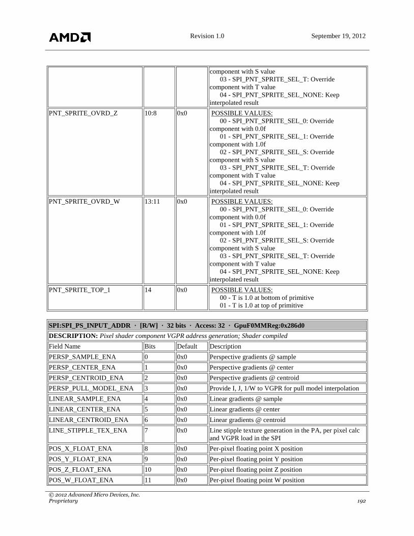
Revision 1.0 September 19, 2012
© 2012 Advanced Micro Devices, Inc. Proprietary 192
component with S value
03 - SPI_PNT_SPRITE_SEL_T: Override
component with T value
04 - SPI_PNT_SPRITE_SEL_NONE: Keep
interpolated result
PNT_SPRITE_OVRD_Z 10:8 0x0 POSSIBLE VALUES:
00 - SPI_PNT_SPRITE_SEL_0: Override
component with 0.0f
01 - SPI_PNT_SPRITE_SEL_1: Override
component with 1.0f
02 - SPI_PNT_SPRITE_SEL_S: Override
component with S value
03 - SPI_PNT_SPRITE_SEL_T: Override
component with T value
04 - SPI_PNT_SPRITE_SEL_NONE: Keep
interpolated result
PNT_SPRITE_OVRD_W 13:11 0x0 POSSIBLE VALUES:
00 - SPI_PNT_SPRITE_SEL_0: Override
component with 0.0f
01 - SPI_PNT_SPRITE_SEL_1: Override
component with 1.0f
02 - SPI_PNT_SPRITE_SEL_S: Override
component with S value
03 - SPI_PNT_SPRITE_SEL_T: Override
component with T value
04 - SPI_PNT_SPRITE_SEL_NONE: Keep
interpolated result
PNT_SPRITE_TOP_1 14 0x0 POSSIBLE VALUES:
00 - T is 1.0 at bottom of primitive
01 - T is 1.0 at top of primitive
SPI:SPI_PS_INPUT_ADDR · [R/W] · 32 bits · Access: 32 · GpuF0MMReg:0x286d0
DESCRIPTION: Pixel shader component VGPR address generation; Shader compiled
Field Name Bits Default Description
PERSP_SAMPLE_ENA 0 0x0 Perspective gradients @ sample
PERSP_CENTER_ENA 1 0x0 Perspective gradients @ center
PERSP_CENTROID_ENA 2 0x0 Perspective gradients @ centroid
PERSP_PULL_MODEL_ENA 3 0x0 Provide I, J, 1/W to VGPR for pull model interpolation
LINEAR_SAMPLE_ENA 4 0x0 Linear gradients @ sample
LINEAR_CENTER_ENA 5 0x0 Linear gradients @ center
LINEAR_CENTROID_ENA 6 0x0 Linear gradients @ centroid
LINE_STIPPLE_TEX_ENA 7 0x0 Line stipple texture generation in the PA, per pixel calc
and VGPR load in the SPI
POS_X_FLOAT_ENA 8 0x0 Per-pixel floating point X position
POS_Y_FLOAT_ENA 9 0x0 Per-pixel floating point Y position
POS_Z_FLOAT_ENA 10 0x0 Per-pixel floating point Z position
POS_W_FLOAT_ENA 11 0x0 Per-pixel floating point W position

Revision 1.0 September 19, 2012
© 2012 Advanced Micro Devices, Inc. Proprietary 193
FRONT_FACE_ENA 12 0x0 Front face
ANCILLARY_ENA 13 0x0 Render target array index[26:16], Iterated sample
number[11:8], Primitive type[1:0]
SAMPLE_COVERAGE_ENA 14 0x0 Sample coverage
POS_FIXED_PT_ENA 15 0x0 Per-pixel fixed point position Y[31:16], X[15:0]
SPI:SPI_PS_INPUT_CNTL_[0-31] · [R/W] · 32 bits · Access: 32 · GpuF0MMReg:0x28644-0x286c0
DESCRIPTION: PS interpolator setttings for parameter 0
Field Name Bits Default Description
OFFSET 5:0 0x0 PS input offset. [4:0] specifies attribute src location in
param cache (VS output number), [5] is used to specify
there was no VS match and tells SPI to use
DEFAULT_VAL for the attribute. If OFFSET[5] and
flat_shade are both set then param cache data is read in
passthrough mode, loading P0,P1,P2 as-is into the LDS.
DEFAULT_VAL 9:8 0x0 Selects value to force into GPR if no semantic match
found
POSSIBLE VALUES:
00 - 0.0f, 0.0f, 0.0f, 0.0f
01 - 0.0f, 0.0f, 0.0f, 1.0f
02 - 1.0f, 1.0f, 1.0f, 0.0f
03 - 1,0f, 1.0f, 1.0f, 1.0f
FLAT_SHADE 10 0x0 Flat shade select. If OFFSET[5] and flat_shade are both
set then param cache data is read in passthrough mode,
loading P0,P1,P2 as-is into the LDS.
CYL_WRAP 16:13 0x0 4-bit cylindrical wrap control (1 bit per component)
PT_SPRITE_TEX 17 0x0 Override this parameter with texture coordinates if global
enable set and prim is a point
DUP 18 0x0 The vtx shader wrote this attribute to both halves of the
param cache and it can be read on either phase
SPI:SPI_PS_INPUT_ENA · [R/W] · 32 bits · Access: 32 · GpuF0MMReg:0x286cc
DESCRIPTION: Pixel shader interpolation control and VGPR load control; Driver generated
Field Name Bits Default Description
PERSP_SAMPLE_ENA 0 0x0 Perspective gradients @ sample
PERSP_CENTER_ENA 1 0x0 Perspective gradients @ center
PERSP_CENTROID_ENA 2 0x0 Perspective gradients @ centroid
PERSP_PULL_MODEL_ENA 3 0x0 Provide I, J, 1/W to VGPR for pull model interpolation
LINEAR_SAMPLE_ENA 4 0x0 Linear gradients @ sample
LINEAR_CENTER_ENA 5 0x0 Linear gradients @ center
LINEAR_CENTROID_ENA 6 0x0 Linear gradients @ centroid
LINE_STIPPLE_TEX_ENA 7 0x0 Line stipple texture generation in the PA, per pixel calc
and VGPR load in the SPI
POS_X_FLOAT_ENA 8 0x0 Per-pixel floating point X position
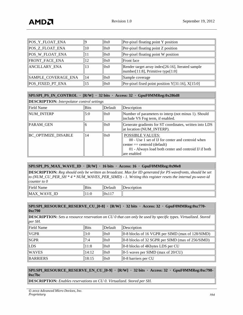
Revision 1.0 September 19, 2012
© 2012 Advanced Micro Devices, Inc. Proprietary 194
POS_Y_FLOAT_ENA 9 0x0 Per-pixel floating point Y position
POS_Z_FLOAT_ENA 10 0x0 Per-pixel floating point Z position
POS_W_FLOAT_ENA 11 0x0 Per-pixel floating point W position
FRONT_FACE_ENA 12 0x0 Front face
ANCILLARY_ENA 13 0x0 Render target array index[26:16], Iterated sample
number[11:8], Primitive type[1:0]
SAMPLE_COVERAGE_ENA 14 0x0 Sample coverage
POS_FIXED_PT_ENA 15 0x0 Per-pixel fixed point position Y[31:16], X[15:0]
SPI:SPI_PS_IN_CONTROL · [R/W] · 32 bits · Access: 32 · GpuF0MMReg:0x286d8
DESCRIPTION: Interpolator control settings
Field Name Bits Default Description
NUM_INTERP 5:0 0x0 Number of parameters to interp (not minus 1). Should
include VS Fog term, if enabled.
PARAM_GEN 6 0x0 Generate gradients for ST coordinates, written into LDS
at location (NUM_INTERP).
BC_OPTIMIZE_DISABLE 14 0x0 POSSIBLE VALUES:
00 - Use 1 set of IJ for center and centroid when
center == centroid (default)
01 - Always load both center and centroid IJ if both
are enabled
SPI:SPI_PS_MAX_WAVE_ID · [R/W] · 16 bits · Access: 16 · GpuF0MMReg:0x90e8
DESCRIPTION: Reg should only be written as broadcast. Max for ID generated for PS wavefronts, should be set
to (NUM_CU_PER_SH * 4 * NUM_WAVES_PER_SIMD) - 1. Writing this register resets the internal ps-wave-id
counter to 0
Field Name Bits Default Description
MAX_WAVE_ID 11:0 0x117
SPI:SPI_RESOURCE_RESERVE_CU_[0-8] · [R/W] · 32 bits · Access: 32 · GpuF0MMReg:0xc770-
0xc790
DESCRIPTION: Sets a resource reservation on CU 0 that can only be used by specific types. Virtualized. Stored
per SH.
Field Name Bits Default Description
VGPR 3:0 0x0 0-8 blocks of 16 VGPR per SIMD (max of 128/SIMD)
SGPR 7:4 0x0 0-8 blocks of 32 SGPR per SIMD (max of 256/SIMD)
LDS 11:8 0x0 0-8 blocks of 4Kbytes LDS per CU
WAVES 14:12 0x0 0-5 waves per SIMD (max of 20/CU)
BARRIERS 18:15 0x0 0-8 barriers per CU
SPI:SPI_RESOURCE_RESERVE_EN_CU_[0-9] · [R/W] · 32 bits · Access: 32 · GpuF0MMReg:0xc798-
0xc7bc
DESCRIPTION: Enables reservations on CU 0. Virtualized. Stored per SH.

Revision 1.0 September 19, 2012
© 2012 Advanced Micro Devices, Inc. Proprietary 195
Field Name Bits Default Description
EN 0 0x0 Enable reservation on this CU
TYPE_MASK 15:1 0x0 Types that are allowed to use reserved space. 0->6 =
GFX_PS->CS, 7->14 = CS0->CS7
QUEUE_MASK 23:16 0x0 Queues that are allowed to use reserved space. 0->7 =
QueueSlot0-7 for all enabled compute pipes in the type
mask
RESERVE_SPACE_ONLY 24 0x0 Mode bit for matching source use of reservation space.
The RESERVE_SPACE_ONLY feature is only honored
for compute only reservations. If the TYPE_MASK
includes any GFX_* Task in the reservation this bit will
be forced to 0 and prevent the use of
RESERVE_SPACE_ONLY feature.
POSSIBLE VALUES:
00 - Use both the available reserved and non-reserved
space
01 - Use only the available reserved space (must be
used in conjunction with CU enable mask for the given
task type)
SPI:SPI_TMPRING_SIZE · [R/W] · 32 bits · Access: 32 · GpuF0MMReg:0x286e8
DESCRIPTION: Temp Ring Size for GFX - PS, VS, GS, ES, HS, LS
Field Name Bits Default Description
WAVES 11:0 0x0 Total size of allocated region in number of waves. Max
is 32 per CU. Scratch wave_slots are not tied directly to
CU, but the max number of waves we want in flight is a
function of the number of CU in the system.
WAVESIZE 24:12 0x0 Amount of space used by each wave in dwords, format is
[20:8] since each wave is 64 threads (6 bits). The API
specs temp space in terms of 4 dword (component)
vectors per thread up to a max of 4K 4-component
vectors (16K * 64 threads = 1M dwords per wave), plus
the driver needs some additional space. The current
register size supports a range of 0->(2M-1) dwords.
SPI:SPI_VS_OUT_CONFIG · [R/W] · 32 bits · Access: 32 · GpuF0MMReg:0x286c4
DESCRIPTION: VS output configuration
Field Name Bits Default Description
VS_EXPORT_COUNT 5:1 0x0 Number of vectors exported by the VS (value is minus 1)
VS_HALF_PACK 6 0x0 Setting this bit causes the VGT to only load VS
wavefronts half full of verts and the SPI to alloc/dealloc
half the param cache space for each wave. Required for
configs with > 1 quad pipe when
(((VS_EXPORT_COUNT + 1) *
GPU__GC__QP_PER_SIMD * 2 ) >
GPU__SX__PARAMETER_CACHE_DEPTH)

Revision 1.0 September 19, 2012
© 2012 Advanced Micro Devices, Inc. Proprietary 196
11. Compute Registers
COMP:COMPUTE_DIM_X · [W] · 32 bits · Access: 32 · GpuF0MMReg:0xb804
DESCRIPTION: Ring-specific: Used to specify number of threadgroups in the X dim
Field Name Bits Default Description
SIZE 31:0 none X dimension of number of threadgroups, if set to 0, or
less than or equal to START_X, no work is dispatched
COMP:COMPUTE_DIM_Y · [W] · 32 bits · Access: 32 · GpuF0MMReg:0xb808
DESCRIPTION: Ring-specific: Used to specify number of threadgroups in the Y dim
Field Name Bits Default Description
SIZE 31:0 none Y dimension of number of threadgroups, if set to 0, or
less than or equal to START_Y, no work is dispatched
COMP:COMPUTE_DIM_Z · [W] · 32 bits · Access: 32 · GpuF0MMReg:0xb80c
DESCRIPTION: Ring-specific: Used to specify number of threadgroups in the Z dim
Field Name Bits Default Description
SIZE 31:0 none Z dimension of number of threadgroups, if set to 0, or
less than or equal to START_Z, no work is dispatched
COMP:COMPUTE_DISPATCH_INITIATOR · [W] · 32 bits · Access: 32 · GpuF0MMReg:0xb800
DESCRIPTION: Processes one Dispatch Command based on current Compute state.
Field Name Bits Default Description
COMPUTE_SHADER_EN 0 none If 1, process this dispatch initiator. If 0, discard it
PARTIAL_TG_EN 1 none If 1, respect partial threadgroup settings, if 0, ignore
them
FORCE_START_AT_000 2 none If 1, override each of COMPUTE_START_X/Y/Z to 0
ORDERED_APPEND_ENBL 3 none If 1, support ordered append, (IA will generate a wave_id
base value for each threadgroup, SPI will subsequently
use this value to generate a unique value for each wave
generated for the threadgroup. This value is loaded to an
SGPR )
ORDERED_APPEND_MODE 4 none 0: Unique wave-id per wave. 1: Unique wave-id per
Threadgroup
USE_THREAD_DIMENSIONS 5 none If 1, the ADC will receive the total number of
threads(x/y/z) in a dispatch and the
NUM_THREADS_FULL(x/y/z) and the ADC will have
to calculate the DIM_X/Y/Z values, and calculate the
NUM_THREADS_PARTIAL
ORDER_MODE 6 none 0: All CS waves in the SPI need to be launched in order.
1: CS Waves can be launched out of order in the SPI
DISPATCH_CACHE_CNTL 9:7 none Bit[2] Enable(0) or Disable(1) Scalar L1; Bit[1]
Enable(0) or Disable(1) L2; Bit[0] Enable(0) or

Revision 1.0 September 19, 2012
© 2012 Advanced Micro Devices, Inc. Proprietary 197
Disable(1) Vector L1
SCALAR_L1_INV_VOL 10 none If 1, Invalidate all volatile tagged lines from
scalar(constant) L1 cache(s) used by the dispatch. Once
per scalar L1 invalidation op for the dispatch.
VECTOR_L1_INV_VOL 11 none If 1, Invalidate all volatile tagged lines from vector L1
cache(s) used by the dispatch. Once per CU invalidation
op on vector L1 for the dispatch.
DATA_ATC 12 none
RESTORE 14 none Signals that a context switch restore is occurring and
restart x/y/z values should be used for this dispatch. This
is not a user programmed field, this bit is set by internal
logic when a context switch occurs.
COMP:COMPUTE_NUM_THREAD_X · [W] · 32 bits · Access: 32 · GpuF0MMReg:0xb81c
DESCRIPTION: Compute shader thread group X dimension. 1 means 1 thread, 0 is an invalid setting. Max is 2k
and X*Y*Z max is 2k.
Field Name Bits Default Description
NUM_THREAD_FULL 15:0 none Dimension used when threadgroup is full in X dimension
(PARTIAL_TG_EN == 0 or tgid.X <
COMPUTE_DIM_X).
NUM_THREAD_PARTIAL 31:16 none Dimension used when threadgroup is partial in X
dimension (PARTIAL_TG_EN == 1 and tgid.X ==
COMPUTE_DIM_X).
COMP:COMPUTE_NUM_THREAD_Y · [W] · 32 bits · Access: 32 · GpuF0MMReg:0xb820
DESCRIPTION: Compute shader thread group Y dimension. 1 means 1 thread, 0 is an invalid setting. Max is 2k
and X*Y*Z max is 2k.
Field Name Bits Default Description
NUM_THREAD_FULL 15:0 none Dimension used when threadgroup is full in Y dimension
(PARTIAL_TG_EN == 0 or tgid.Y <
COMPUTE_DIM_Y).
NUM_THREAD_PARTIAL 31:16 none Dimension used when threadgroup is partial in Y
dimension (PARTIAL_TG_EN == 1 and tgid.Y ==
COMPUTE_DIM_Y).
COMP:COMPUTE_NUM_THREAD_Z · [W] · 32 bits · Access: 32 · GpuF0MMReg:0xb824
DESCRIPTION: Compute shader thread group Z dimension. 1 means 1 thread, 0 is an invalid setting. Max is 2k
and X*Y*Z max is 2k.
Field Name Bits Default Description
NUM_THREAD_FULL 15:0 none Dimension used when threadgroup is full in Z dimension
(PARTIAL_TG_EN == 0 or tgid.Z <
COMPUTE_DIM_Z).
NUM_THREAD_PARTIAL 31:16 none Dimension used when threadgroup is partial in Z
dimension (PARTIAL_TG_EN == 1 and tgid.Z ==
COMPUTE_DIM_Z).

Revision 1.0 September 19, 2012
© 2012 Advanced Micro Devices, Inc. Proprietary 198
COMP:COMPUTE_PGM_HI · [W] · 32 bits · Access: 32 · GpuF0MMReg:0xb834
Field Name Bits Default Description
DATA 7:0 none
INST_ATC 8 none
COMP:COMPUTE_PGM_LO · [W] · 32 bits · Access: 32 · GpuF0MMReg:0xb830
Field Name Bits Default Description
DATA 31:0 none
COMP:COMPUTE_PGM_RSRC1 · [W] · 32 bits · Access: 32 · GpuF0MMReg:0xb848
DESCRIPTION: Shader program settings for CS
Field Name Bits Default Description
VGPRS 5:0 none Number of VGPRS, granularity 4. Range is from 0-63
allocating 4,8,12 ... 256
SGPRS 9:6 none Number of SGPRS, granularity 8. Range is from 0-15
allocating 8,16,24 ... 128
PRIORITY 11:10 none Drives spi_priority in spi_sq newWave cmd
FLOAT_MODE 19:12 none Drives float_mode in spi_sq newWave cmd
PRIV 20 none Drives priv in spi_sq newWave cmd
DX10_CLAMP 21 none Drives dx10_clamp in spi_sq newWave cmd
DEBUG_MODE 22 none Drives debug in spi_sq newWave cmd
IEEE_MODE 23 none Drives ieee in spi_sq newWave cmd
BULKY 24 none Only one such threadgroup is allowed to be active on any
given Compute Unit
CDBG_USER 25 none
COMP:COMPUTE_PGM_RSRC2 · [W] · 32 bits · Access: 32 · GpuF0MMReg:0xb84c
DESCRIPTION: Shader program settings for CS
Field Name Bits Default Description
SCRATCH_EN 0 none This wave uses scratch space for register spilling
USER_SGPR 5:1 none Number of USER_DATA terms that should be initialized
by SPI. Range is 0-16.
TRAP_PRESENT 6 none Enables trap processing. Sets trap_en bit to SQ and
causes SPI to alloc 16 extra SGPR and write TBA/TMA
values to SGPR.
TGID_X_EN 7 none Enables loading of TGID.X into SGPR
TGID_Y_EN 8 none Enables loading of TGID.Y into SGPR
TGID_Z_EN 9 none Enables loading of TGID.Z into SGPR
TG_SIZE_EN 10 none Enables loading of threadgroup related info to SGPR.
See shader pgm guide for details
TIDIG_COMP_CNT 12:11 none Specifies how many thread_id_in_group terms to write
to VGPR. 0=X, 1=XY, 2=XYZ, 3=Undefined

Revision 1.0 September 19, 2012
© 2012 Advanced Micro Devices, Inc. Proprietary 199
EXCP_EN_MSB 14:13 none
LDS_SIZE 23:15 none Amount of LDS space to alloc for each threadgroup.
Granularity 128, range is 0 to 128 which allocates 0 to
16K dwords.
EXCP_EN 30:24 none Drives excp bits in spi_sq newWave cmd
COMP:COMPUTE_RESOURCE_LIMITS · [W] · 32 bits · Access: 32 · GpuF0MMReg:0xb854
DESCRIPTION: Resource limit and lock threshold setting for CS
Field Name Bits Default Description
WAVES_PER_SH 9:0 none CS wave limit per SH, format is [9:4]. A setting of 1
means 16 waves, 63 means 1008, and 0 disables the
limit.
TG_PER_CU 15:12 none CS threadgroup limit per CU. Range is 1 to 15, 0
disables the limit.
LOCK_THRESHOLD 21:16 none Sets per-SH low threshold for locking. Granularity 4, 0
disables locking. If CS has less waves active than its
setting and its allocation does not fit then it can lock a
CU and block other stages from allocating to that CU.
SIMD_DEST_CNTL 22 none 0 = adjust preferred SIMD if there`s a conflict with
previous start for target CU, 1 = don`t adjust and always
prefer DEST SIMD.
FORCE_SIMD_DIST 23 none Force equal SIMD distribution within a CU, ignoring
input bandwidth concerns.
POSSIBLE VALUES:
00 - Try to balance input bandwidth as threadgroups
walk CU (default)
01 - Send to the next SIMD for the chosen CU no
matter what, regardless of where the previous
threadgroup left off.
CU_GROUP_COUNT 26:24 none Number of threadgroups to attempt to send to a CU
before moving on to the next CU. 0= 1 threadgroup, 7= 8
threadgroups.
COMP:COMPUTE_START_X · [W] · 32 bits · Access: 32 · GpuF0MMReg:0xb810
DESCRIPTION: Ring-specific: Used to specify start in X dim for compute threadgroups
Field Name Bits Default Description
START 31:0 none X-dimension of start of threadgroups; normally set to
zero. This is used as the start index, in the X dimension,
for Threadgroup creation.
COMP:COMPUTE_START_Y · [W] · 32 bits · Access: 32 · GpuF0MMReg:0xb814
DESCRIPTION: Ring-specific: Used to specify start in Y dim for compute threadgroups
Field Name Bits Default Description
START 31:0 none Y-dimension of start of threadgroups; normally set to
zero.

Revision 1.0 September 19, 2012
© 2012 Advanced Micro Devices, Inc. Proprietary 200
COMP:COMPUTE_START_Z · [W] · 32 bits · Access: 32 · GpuF0MMReg:0xb818
DESCRIPTION: Ring-specific: Used to specify start in Z dim for compute threadgroups
Field Name Bits Default Description
START 31:0 none Z-dimension of start of threadgroups; normally set to
zero.
COMP:COMPUTE_TBA_HI · [W] · 32 bits · Access: 32 · GpuF0MMReg:0xb83c
Field Name Bits Default Description
DATA 7:0 none
COMP:COMPUTE_TBA_LO · [W] · 32 bits · Access: 32 · GpuF0MMReg:0xb838
Field Name Bits Default Description
DATA 31:0 none
COMP:COMPUTE_TMA_HI · [W] · 32 bits · Access: 32 · GpuF0MMReg:0xb844
Field Name Bits Default Description
DATA 7:0 none
COMP:COMPUTE_TMA_LO · [W] · 32 bits · Access: 32 · GpuF0MMReg:0xb840
Field Name Bits Default Description
DATA 31:0 none
COMP:COMPUTE_TMPRING_SIZE · [W] · 32 bits · Access: 32 · GpuF0MMReg:0xb860
DESCRIPTION: Temp Ring Size for CS
Field Name Bits Default Description
WAVES 11:0 none Total size of allocated region in number of waves. Max
is 32 per total CU in the chip.
WAVESIZE 24:12 none Amount of space used by each wave in dwords. It is in
units of 256 dwords. The field size supports a range of 0-
>(2M-256) dwords per wave.
COMP:COMPUTE_USER_DATA_[0-15] · [W] · 32 bits · Access: 32 · GpuF0MMReg:0xb900-0xb93c
Field Name Bits Default Description
DATA 31:0 none
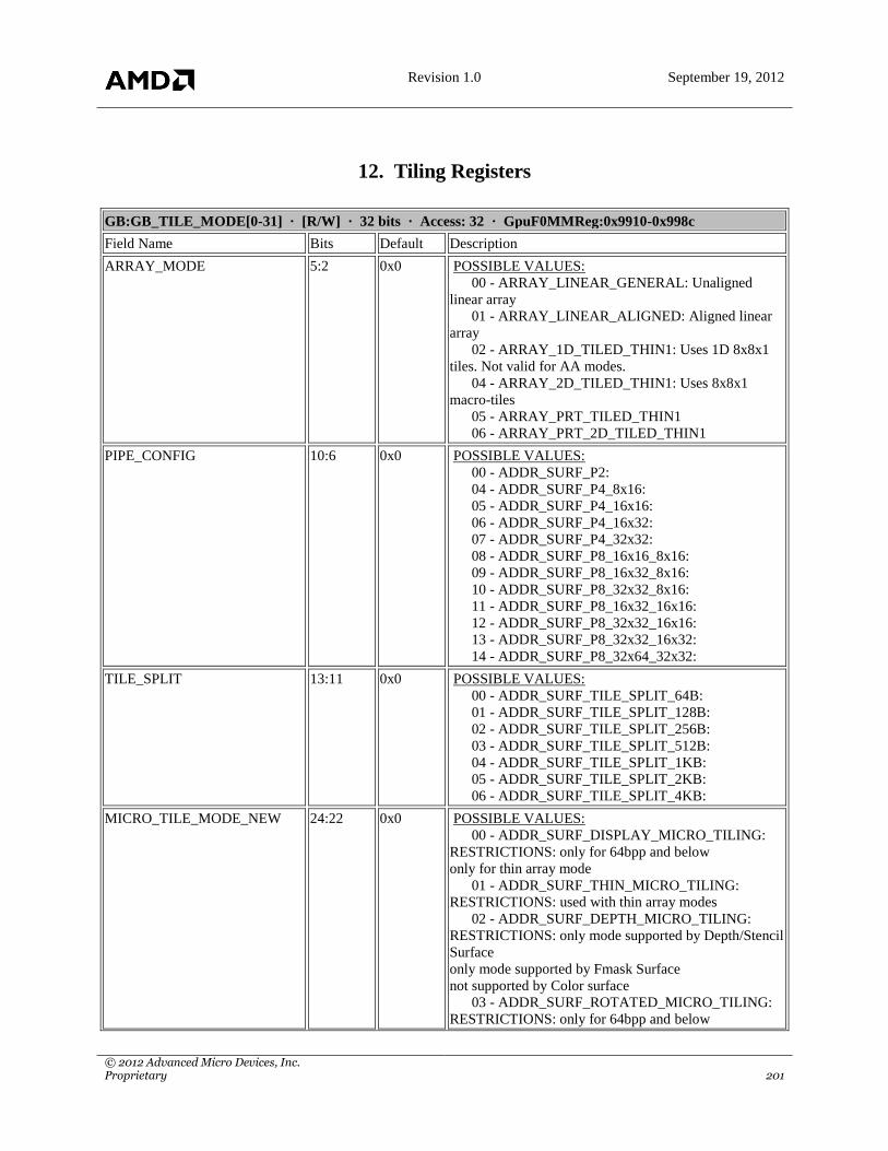
Revision 1.0 September 19, 2012
© 2012 Advanced Micro Devices, Inc. Proprietary 201
12. Tiling Registers
GB:GB_TILE_MODE[0-31] · [R/W] · 32 bits · Access: 32 · GpuF0MMReg:0x9910-0x998c
Field Name Bits Default Description
ARRAY_MODE 5:2 0x0 POSSIBLE VALUES:
00 - ARRAY_LINEAR_GENERAL: Unaligned
linear array
01 - ARRAY_LINEAR_ALIGNED: Aligned linear
array
02 - ARRAY_1D_TILED_THIN1: Uses 1D 8x8x1
tiles. Not valid for AA modes.
04 - ARRAY_2D_TILED_THIN1: Uses 8x8x1
macro-tiles
05 - ARRAY_PRT_TILED_THIN1
06 - ARRAY_PRT_2D_TILED_THIN1
PIPE_CONFIG 10:6 0x0 POSSIBLE VALUES:
00 - ADDR_SURF_P2:
04 - ADDR_SURF_P4_8x16:
05 - ADDR_SURF_P4_16x16:
06 - ADDR_SURF_P4_16x32:
07 - ADDR_SURF_P4_32x32:
08 - ADDR_SURF_P8_16x16_8x16:
09 - ADDR_SURF_P8_16x32_8x16:
10 - ADDR_SURF_P8_32x32_8x16:
11 - ADDR_SURF_P8_16x32_16x16:
12 - ADDR_SURF_P8_32x32_16x16:
13 - ADDR_SURF_P8_32x32_16x32:
14 - ADDR_SURF_P8_32x64_32x32:
TILE_SPLIT 13:11 0x0 POSSIBLE VALUES:
00 - ADDR_SURF_TILE_SPLIT_64B:
01 - ADDR_SURF_TILE_SPLIT_128B:
02 - ADDR_SURF_TILE_SPLIT_256B:
03 - ADDR_SURF_TILE_SPLIT_512B:
04 - ADDR_SURF_TILE_SPLIT_1KB:
05 - ADDR_SURF_TILE_SPLIT_2KB:
06 - ADDR_SURF_TILE_SPLIT_4KB:
MICRO_TILE_MODE_NEW 24:22 0x0 POSSIBLE VALUES:
00 - ADDR_SURF_DISPLAY_MICRO_TILING:
RESTRICTIONS: only for 64bpp and below
only for thin array mode
01 - ADDR_SURF_THIN_MICRO_TILING:
RESTRICTIONS: used with thin array modes
02 - ADDR_SURF_DEPTH_MICRO_TILING:
RESTRICTIONS: only mode supported by Depth/Stencil
Surface
only mode supported by Fmask Surface
not supported by Color surface
03 - ADDR_SURF_ROTATED_MICRO_TILING:
RESTRICTIONS: only for 64bpp and below

Revision 1.0 September 19, 2012
© 2012 Advanced Micro Devices, Inc. Proprietary 202
only for thin array mode
SAMPLE_SPLIT 26:25 0x0 POSSIBLE VALUES:
00 - ADDR_SURF_SAMPLE_SPLIT_1: Tile split
on every 1 sample
01 - ADDR_SURF_SAMPLE_SPLIT_2: Tile split
on every 2 samples
02 - ADDR_SURF_SAMPLE_SPLIT_4: Tile split
on every 4 samples
03 - ADDR_SURF_SAMPLE_SPLIT_8: Tile split
on every 8 samples
GB:GB_MACROTILE_MODE[0-15] · [R/W] · 32 bits · Access: 32 · GpuF0MMReg:0x9990-0x99cc
Field Name Bits Default Description
BANK_WIDTH 1:0 0x0 POSSIBLE VALUES:
00 - ADDR_SURF_BANK_WIDTH_1:
01 - ADDR_SURF_BANK_WIDTH_2:
02 - ADDR_SURF_BANK_WIDTH_4:
03 - ADDR_SURF_BANK_WIDTH_8:
BANK_HEIGHT 3:2 0x0 POSSIBLE VALUES:
00 - ADDR_SURF_BANK_HEIGHT_1:
01 - ADDR_SURF_BANK_HEIGHT_2:
02 - ADDR_SURF_BANK_HEIGHT_4:
03 - ADDR_SURF_BANK_HEIGHT_8:
MACRO_TILE_ASPECT 5:4 0x0 POSSIBLE VALUES:
00 - ADDR_SURF_MACRO_ASPECT_1:
01 - ADDR_SURF_MACRO_ASPECT_2:
02 - ADDR_SURF_MACRO_ASPECT_4:
03 - ADDR_SURF_MACRO_ASPECT_8:
NUM_BANKS 7:6 0x0 POSSIBLE VALUES:
00 - ADDR_SURF_2_BANK:
01 - ADDR_SURF_4_BANK:
02 - ADDR_SURF_8_BANK:
03 - ADDR_SURF_16_BANK:
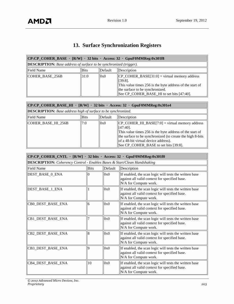
Revision 1.0 September 19, 2012
© 2012 Advanced Micro Devices, Inc. Proprietary 203
13. Surface Synchronization Registers
CP:CP_COHER_BASE · [R/W] · 32 bits · Access: 32 · GpuF0MMReg:0x301f8
DESCRIPTION: Base address of surface to be synchronized (trigger).
Field Name Bits Default Description
COHER_BASE_256B 31:0 0x0 CP_COHER_BASE[31:0] = virtual memory address
[39:8].
This value times 256 is the byte address of the start of
the surface to be synchronized.
See CP_COHER_BASE_HI to set bits [47:40].
CP:CP_COHER_BASE_HI · [R/W] · 32 bits · Access: 32 · GpuF0MMReg:0x301e4
DESCRIPTION: Base address high of surface to be synchronized.
Field Name Bits Default Description
COHER_BASE_HI_256B 7:0 0x0 CP_COHER_HI_BASE[7:0] = virtual memory address
[47:40].
This value times 256 is the byte address of the start of
the surface to be synchronized (to create the high 8-bits
of a 48-bit virtual device address).
See CP_COHER_BASE to set bits [39:8].
CP:CP_COHER_CNTL · [R/W] · 32 bits · Access: 32 · GpuF0MMReg:0x301f0
DESCRIPTION: Coherency Control - Enables Bases & Start/Clean Handshaking
Field Name Bits Default Description
DEST_BASE_0_ENA 0 0x0 If enabled, the scan logic will tests the written base
against all valid context for specified base.
N/A for Compute work.
DEST_BASE_1_ENA 1 0x0 If enabled, the scan logic will tests the written base
against all valid context for specified base.
N/A for Compute work.
CB0_DEST_BASE_ENA 6 0x0 If enabled, the scan logic will tests the written base
against all valid context for specified base.
N/A for Compute work.
CB1_DEST_BASE_ENA 7 0x0 If enabled, the scan logic will tests the written base
against all valid context for specified base.
N/A for Compute work.
CB2_DEST_BASE_ENA 8 0x0 If enabled, the scan logic will tests the written base
against all valid context for specified base.
N/A for Compute work.
CB3_DEST_BASE_ENA 9 0x0 If enabled, the scan logic will tests the written base
against all valid context for specified base.
N/A for Compute work.
CB4_DEST_BASE_ENA 10 0x0 If enabled, the scan logic will tests the written base
against all valid context for specified base.
N/A for Compute work.

Revision 1.0 September 19, 2012
© 2012 Advanced Micro Devices, Inc. Proprietary 204
CB5_DEST_BASE_ENA 11 0x0 If enabled, the scan logic will tests the written base
against all valid context for specified base.
N/A for Compute work.
CB6_DEST_BASE_ENA 12 0x0 If enabled, the scan logic will tests the written base
against all valid context for specified base.
N/A for Compute work.
CB7_DEST_BASE_ENA 13 0x0 If enabled, the scan logic will tests the written base
against all valid context for specified base.
N/A for Compute work.
DB_DEST_BASE_ENA 14 0x0 If enabled, the scan logic will tests the written base
against all valid context for specified base.
N/A for Compute work.
TCL1_VOL_ACTION_ENA 15 0x0
TC_VOL_ACTION_ENA 16 0x0
TC_WB_ACTION_ENA 18 0x0 If enabled, indicates that a write back action is
requested.
DEST_BASE_2_ENA 19 0x0 If enabled, the scan logic will tests the written base
against all valid context for specified base.
N/A for Compute work.
DEST_BASE_3_ENA 21 0x0 If enabled, the scan logic will tests the written base
against all valid context for specified base.
N/A for Compute work.
TCL1_ACTION_ENA 22 0x0 If enabled, the L1 cache will get invalidated when the
Coher_Base is written (CP sends write to TC with
OP=WBINVL1).
TC_ACTION_ENA 23 0x0 If enabled, the L2 cache will get invalidated when the
Coher_Base is written (CP sends write to TC with
OP=WBINVL2).
CB_ACTION_ENA 25 0x0 If enabled, this cache will get a Start signal when the
Coher_Base is written.
DB_ACTION_ENA 26 0x0 If enabled, this cache will get a Start signal when the
Coher_Base is written.
SH_KCACHE_ACTION_ENA 27 0x0 If enabled, this cache will get a Start signal when the
Coher_Base is written.
If the SH_KCACHE_VOL_ACTION_ENA bit is also
set, then action will only be taken on the volatile
contents of the cache - otherwise, action will be take on
the entire cache.
SH_KCACHE_VOL_ACTION_ENA 28 0x0 If enabled, this cache will get a Start signal when the
Coher_Base is written. Action will only be taken on the
Volatile contents of the cache. This volatile action
enable is qualified by the
SH_KCACHE_ACTION_ENA bit being set. If the
SH_KCACHE_ACTION_EN bit is not set, then the
SH_KCACHE_VOL_ACTION_ENA bit has no
meaning and no action will be taken.
SH_ICACHE_ACTION_ENA 29 0x0 If enabled, this cache will get a Start signal when the
Coher_Base is written.

Revision 1.0 September 19, 2012
© 2012 Advanced Micro Devices, Inc. Proprietary 205
CP:CP_COHER_SIZE · [R/W] · 32 bits · Access: 32 · GpuF0MMReg:0x301f4
DESCRIPTION: The size of the surface to be synchronized in 256 byte blocks. For example, a 4KB surface would
be programmed to 0x10.
Field Name Bits Default Description
COHER_SIZE_256B 31:0 0x0 CP_COHER_SIZE[31:0] ; Surface Size has a granularity
of 256 Bytes.
See CP_COHER_SIZE_HI to set bits [47:40]
CP:CP_COHER_SIZE_HI · [R/W] · 32 bits · Access: 32 · GpuF0MMReg:0x30230
DESCRIPTION: The size high of the surface to be synchronized in 256 byte blocks. For example, a 4KB surface
would be programmed to 0x10.
Field Name Bits Default Description
COHER_SIZE_HI_256B 7:0 0x0 CP_COHER_SIZE_HI[7:0]

Revision 1.0 September 19, 2012
© 2012 Advanced Micro Devices, Inc. Proprietary 206
14. Texture Pipe Registers
TP:TA_BC_BASE_ADDR · [R/W] · 32 bits · Access: 32 · GpuF0MMReg:0x28080
DESCRIPTION: Base Address of buffer used to store border color values. (Instanced per graphics state context).
Field Name Bits Default Description
ADDRESS 31:0 none bits [39:8] of base address (256-byte aligned)
TP:TA_BC_BASE_ADDR_HI · [R/W] · 32 bits · Access: 32 · GpuF0MMReg:0x28084
DESCRIPTION: Base Address of buffer used to store border color values. (Instanced per graphics state context).
Field Name Bits Default Description
ADDRESS 7:0 none bits [47:40] of base address (256-byte aligned)
TP:TA_CS_BC_BASE_ADDR · [R/W] · 32 bits · Access: 32 · GpuF0MMReg:0x30e00
DESCRIPTION: Base Address of buffer used to store border color values for compute shaders. (Instanced per-
microengine).
Field Name Bits Default Description
ADDRESS 31:0 none bits [39:8] of base address (256-byte aligned)
TP:TA_CS_BC_BASE_ADDR_HI · [R/W] · 32 bits · Access: 32 · GpuF0MMReg:0x30e04
DESCRIPTION: Base Address of buffer used to store border color values for compute shaders. (Instanced per-
microengine).
Field Name Bits Default Description
ADDRESS 7:0 none bits [47:40] of base address (256-byte aligned)

Revision 1.0 September 19, 2012
© 2012 Advanced Micro Devices, Inc. Proprietary 207
15. Depth Buffer Registers
DB:DB_ALPHA_TO_MASK · [R/W] · 32 bits · Access: 32 · GpuF0MMReg:0x28b70
Field Name Bits Default Description
ALPHA_TO_MASK_ENABLE 0 none If enabled, the sample mask is ANDed with a mask produced
from the alpha value. This field can be overriden by setting
DB_SHADER_CONTROL.ALPHA_TO_MASK_DISABLE.
SPI_SHADER_COL_FORMAT.COL0_EXPORT_FORMAT
must have a non-integer alpha channel (32_AR,
FP16_ABGR, UNORM16_ABGR, SNORM_ABGR or
32_ABGR).
ALPHA_TO_MASK_OFFSET0 9:8 none Dither threshold for pixel (0,0) in each quad if alpha to mask
is enabled. Set to 2 for non-dithered, or a unique 0-3 value for
dithered.
ALPHA_TO_MASK_OFFSET1 11:10 none Dither threshold for pixel (0,1) in each quad if alpha to mask
is enabled. Set to 2 for non-dithered, or a unique 0-3 value for
dithered.
ALPHA_TO_MASK_OFFSET2 13:12 none Dither threshold for pixel (1,0) in each quad if alpha to mask
is enabled. Set to 2 for non-dithered, or a unique 0-3 value for
dithered.
ALPHA_TO_MASK_OFFSET3 15:14 none Dither threshold for pixel (1,1) in each quad if alpha to mask
is enabled. Set to 2 for non-dithered, or a unique 0-3 value for
dithered.
OFFSET_ROUND 16 none Round dither threshold. Set to 0 for a non-dithered look, or 1
for a dithered look.
DB:DB_COUNT_CONTROL · [R/W] · 32 bits · Access: 32 · GpuF0MMReg:0x28004
Field Name Bits Default Description
PERFECT_ZPASS_COUNTS 1 none Forces zpass counts to be accurate by turning off no-op
culling optimizations where skipping rasterization may
lead to incorrect zpass counts (partially covered tiles).
SAMPLE_RATE 6:4 0x0 Sets how many samples per pixel are counted. Area is
accurate no matter how many samples per pixel there
really are.
ZPASS_ENABLE 11:8 0x0 Indicates if samples passing z are counted. Each bit
corresponds to one of the (up to) 4 counters
ZFAIL_ENABLE 15:12 0x0 Indicates if samples failing z are counted. Each bit
corresponds to one of the (up to) 4 counters
SFAIL_ENABLE 19:16 0x0 Indicates if samples failing stencil are counted. Each bit
corresponds to one of the (up to) 4 counters
DBFAIL_ENABLE 23:20 0x0 Indicates if samples failing depth bounds are counted.
Each bit corresponds to one of the (up to) 4 counters
SLICE_EVEN_ENABLE 27:24 0x0 Indicates if the counter counts on even slices. Each bit
corresponds to one of the (up to) 4 counters
SLICE_ODD_ENABLE 31:28 0x0 Indicates if the counter counts on odd slices. Each bit

Revision 1.0 September 19, 2012
© 2012 Advanced Micro Devices, Inc. Proprietary 208
corresponds to one of the (up to) 4 counters
DB:DB_DEPTH_BOUNDS_MAX · [R/W] · 32 bits · Access: 32 · GpuF0MMReg:0x28024
Field Name Bits Default Description
MAX 31:0 none Maximum z value for the depth bounds test.
DB:DB_DEPTH_BOUNDS_MIN · [R/W] · 32 bits · Access: 32 · GpuF0MMReg:0x28020
Field Name Bits Default Description
MIN 31:0 none Minimum z value for the depth bounds test.
DB:DB_DEPTH_CLEAR · [R/W] · 32 bits · Access: 32 · GpuF0MMReg:0x2802c
Field Name Bits Default Description
DEPTH_CLEAR 31:0 none Depth value when ZMASK==0, which indicates that the
tile has been cleared to the background depth. This
register holds a 32bit float value. This value must be in
the range of 0.0 to 1.0
DB:DB_DEPTH_CONTROL · [R/W] · 32 bits · Access: 32 · GpuF0MMReg:0x28800
DESCRIPTION: This register controls depth and stencil tests.
Field Name Bits Default Description
STENCIL_ENABLE 0 none Enables stencil testing. If disabled, all pixels
pass the stencil test. If there is no stencil buffer
this is treated as disabled.
Z_ENABLE 1 none Enables depth testing. If disabled, all pixels pass
the depth test. If there is no depth buffer this is
treated as disabled.
Z_WRITE_ENABLE 2 none Enables writing to the depth buffer if the depth
test passes.
DEPTH_BOUNDS_ENABLE 3 none Enables depth bounds test. If disabled all
samples pass the depth bounds test. If there is
no depth buffer this is treated as disabled.
ZFUNC 6:4 none Specifies the function that compares the depth
at each sample in the fragment to the destination
depth at the corresponding sample point.
POSSIBLE VALUES:
00 - FRAG_NEVER: never pass
01 - FRAG_LESS: pass if fragment < dest
02 - FRAG_EQUAL: pass if fragment =
dest
03 - FRAG_LEQUAL: pass if fragment <=
dest
04 - FRAG_GREATER: pass if fragment >
dest
05 - FRAG_NOTEQUAL: pass if fragment
!= dest

Revision 1.0 September 19, 2012
© 2012 Advanced Micro Devices, Inc. Proprietary 209
06 - FRAG_GEQUAL: pass if fragment >=
dest
07 - FRAG_ALWAYS: always pass
BACKFACE_ENABLE 7 none If false, forces all quads to be stencil tested as
frontface quads.
STENCILFUNC 10:8 none Specifies the function that compares
STENCILREF to the destination stencil value
for frontface quads. The stencil test passes if ref
OP dest is true.
POSSIBLE VALUES:
00 - REF_NEVER: never pass
01 - REF_LESS: pass if left < right
02 - REF_EQUAL: pass if left = right
03 - REF_LEQUAL: pass if left <= right
04 - REF_GREATER: pass if left > right
05 - REF_NOTEQUAL: pass if left != right
06 - REF_GEQUAL: pass if left >= right
07 - REF_ALWAYS: always pass
STENCILFUNC_BF 22:20 none Specifies the function that compares
STENCILREF_BF to the destination stencil for
backface quads. The stencil test passes if ref OP
dest is true.
POSSIBLE VALUES:
00 - REF_NEVER: never pass
01 - REF_LESS: pass if left < right
02 - REF_EQUAL: pass if left = right
03 - REF_LEQUAL: pass if left <= right
04 - REF_GREATER: pass if left > right
05 - REF_NOTEQUAL: pass if left != right
06 - REF_GEQUAL: pass if left >= right
07 - REF_ALWAYS: always pass
ENABLE_COLOR_WRITES_ON_DEPTH_FAIL 30 none Enables writes to the color buffer if z or stencil
fail.
DISABLE_COLOR_WRITES_ON_DEPTH_PASS 31 none Disables writes to the color buffer if z and
stencil pass.
DB:DB_DEPTH_INFO · [R/W] · 32 bits · Access: 32 · GpuF0MMReg:0x2803c
Field Name Bits Default Description
ADDR5_SWIZZLE_MASK 3:0 none For 32B tiles, indicates whether the data should be stored
in the upper or lower half of a 64B word. if the XOR
reduce of ADDR5_SWIZZLE_MASK & {TILE_Y[1:0],
TILE_X[1:0]} is set, use the upper half, otherwise, use
the lower half. Most likely best value is 0x1.
ARRAY_MODE 7:4 none Specifies the tiling format of this MRT.
POSSIBLE VALUES:
00 - ARRAY_LINEAR_GENERAL: Unaligned
linear array
01 - ARRAY_LINEAR_ALIGNED: Aligned linear
array
02 - ARRAY_1D_TILED_THIN1: Uses 1D 8x8x1

Revision 1.0 September 19, 2012
© 2012 Advanced Micro Devices, Inc. Proprietary 210
tiles. Not valid for AA modes.
04 - ARRAY_2D_TILED_THIN1: Uses 8x8x1
macro-tiles
05 - ARRAY_PRT_TILED_THIN1:
06 - ARRAY_PRT_2D_TILED_THIN1:
PIPE_CONFIG 12:8 none Specifies both the number of pipes and how pipes are
interleaved on the surface.
POSSIBLE VALUES:
00 - ADDR_SURF_P2:
04 - ADDR_SURF_P4_8x16:
05 - ADDR_SURF_P4_16x16:
06 - ADDR_SURF_P4_16x32:
07 - ADDR_SURF_P4_32x32:
08 - ADDR_SURF_P8_16x16_8x16:
09 - ADDR_SURF_P8_16x32_8x16:
10 - ADDR_SURF_P8_32x32_8x16:
11 - ADDR_SURF_P8_16x32_16x16:
12 - ADDR_SURF_P8_32x32_16x16:
13 - ADDR_SURF_P8_32x32_16x32:
14 - ADDR_SURF_P8_32x64_32x32:
BANK_WIDTH 14:13 none Specifies the number of tiles in the x direction to be
incorporated into the same bank. Only applies to 2D
tiling modes.
POSSIBLE VALUES:
00 - ADDR_SURF_BANK_WIDTH_1:
01 - ADDR_SURF_BANK_WIDTH_2:
02 - ADDR_SURF_BANK_WIDTH_4:
03 - ADDR_SURF_BANK_WIDTH_8:
BANK_HEIGHT 16:15 none Specifies the number of tiles in the y direction to be
incorporated into the same bank. Only applies to 2D
tiling modes. (Note: Fmask uses a different register field
for bank height.)
POSSIBLE VALUES:
00 - ADDR_SURF_BANK_HEIGHT_1:
01 - ADDR_SURF_BANK_HEIGHT_2:
02 - ADDR_SURF_BANK_HEIGHT_4:
03 - ADDR_SURF_BANK_HEIGHT_8:
MACRO_TILE_ASPECT 18:17 none Specifies the macro tile aspect ratio. Only applies to 2D
tiling modes.
POSSIBLE VALUES:
00 - ADDR_SURF_MACRO_ASPECT_1:
01 - ADDR_SURF_MACRO_ASPECT_2:
02 - ADDR_SURF_MACRO_ASPECT_4:
03 - ADDR_SURF_MACRO_ASPECT_8:
NUM_BANKS 20:19 none Specifies the number of memory banks for tiling
purposes.
POSSIBLE VALUES:
00 - ADDR_SURF_2_BANK:
01 - ADDR_SURF_4_BANK:
02 - ADDR_SURF_8_BANK:
03 - ADDR_SURF_16_BANK:
Revision 1.0 September 19, 2012
© 2012 Advanced Micro Devices, Inc. Proprietary 211
DB:DB_DEPTH_SIZE · [R/W] · 32 bits · Access: 32 · GpuF0MMReg:0x28058
Field Name Bits Default Description
PITCH_TILE_MAX 10:0 none Width in 8x8 pixel tiles. (Pitch/8 - 1)
HEIGHT_TILE_MAX 21:11 none Height of the depth buffer in 8x8 pixels (height/8 - 1)
DB:DB_DEPTH_SLICE · [R/W] · 32 bits · Access: 32 · GpuF0MMReg:0x2805c
Field Name Bits Default Description
SLICE_TILE_MAX 21:0 none Number of 8x8 pixel tiles until the next slice plus some
small number to be able to rotate the tile pattern.
(pitch*height/64 - 1)
DB:DB_DEPTH_VIEW · [R/W] · 32 bits · Access: 32 · GpuF0MMReg:0x28008
DESCRIPTION: Selects slice index range for render target 0.
Field Name Bits Default Description
SLICE_START 10:0 none Specifies the starting slice number for this view. This
field is added to the RenderTargetArrayIndex to compute
the slice to render. SLICE_START must less than or
equal to SLICE_MAX
SLICE_MAX 23:13 none Specifies the maximum allowed Z slice index for this
resource, which is one less than the total number of
slices.
Z_READ_ONLY 24 none read only Z buffer. i.e. Force off writes to Z buffer
STENCIL_READ_ONLY 25 none read only Stencil buffer.i.e. Force off writes to Stencil
buffer
DB:DB_EQAA · [R/W] · 32 bits · Access: 32 · GpuF0MMReg:0x28804
DESCRIPTION: This register controls EQAA in the DB.
Field Name Bits Default Description
MAX_ANCHOR_SAMPLES 2:0 none Sets the most number of anchor samples that the CB
is allowed to use. Set this to the minimum allocated
sample amount of the DB surfaces to limit the
potential of needing the CB to toss non-anchored
fragments after they are created.
PS_ITER_SAMPLES 6:4 none Specifies how many samples to iterate across when
PS_ITER_SAMPLE is set thus setting the amount of
super-sampling.
Typically this is the number of app exposed
samples. Values greater than the depth surface
samples is not supported.
MASK_EXPORT_NUM_SAMPLES 10:8 none Specifies how many samples to use for shader mask
exports.
ALPHA_TO_MASK_NUM_SAMPLES 14:12 none How many samples of quality are generated for
A2M. Set this in between the number of app
exposed samples and higher EQAA samples for
speed/quality tradeoff. If

Revision 1.0 September 19, 2012
© 2012 Advanced Micro Devices, Inc. Proprietary 212
ALPHA_TO_MASK_EQAA_DISABLE=1, it must
be set to the number of app exposed samples.
HIGH_QUALITY_INTERSECTIONS 16 none
INCOHERENT_EQAA_READS 17 none
INTERPOLATE_COMP_Z 18 none
INTERPOLATE_SRC_Z 19 none
STATIC_ANCHOR_ASSOCIATIONS 20 none
ALPHA_TO_MASK_EQAA_DISABLE 21 none Makes Alpha to Mask set samples exactly like the
previous GPUs. Should only be set if previous
generation behavior is desired, otherwise the new
behavior is optimized for EQAA which improves
the quality when mixing AA modes and even when
not.
OVERRASTERIZATION_AMOUNT 26:24 none Log2 of the number of times to or reduce the sample
mask for over rasterization
ENABLE_POSTZ_OVERRASTERIZATION 27 none Enables overrasterization in postz (ie, after the
shader)
DB:DB_HTILE_DATA_BASE · [R/W] · 32 bits · Access: 32 · GpuF0MMReg:0x28014
Field Name Bits Default Description
BASE_256B 31:0 none Location of the first byte of the HTileData surface in
Device Address Space, which must be 256 byte aligned.
High 32-bits of 40-bit address. This surface contains the
HiZ data.
DB:DB_HTILE_SURFACE · [R/W] · 32 bits · Access: 32 · GpuF0MMReg:0x28abc
Field Name Bits Default Description
LINEAR 0 none Surface is stored linearly in swaths of 8 htiles high until
the surface is complete.
FULL_CACHE 1 none This htile buffer uses the entire htile cache.
if set to 0 and the htile surface will not fit in half the
cache, then the SC`s partial vector deadlock timer must
also be enabled
HTILE_USES_PRELOAD_WIN 2 none If set, the htile surface dimensions will be that of the
preload window; otherwise, it will be that of the depth
buffer
PRELOAD 3 none Preload all data that fits as soon as room is available
once the VGT_DRAW_INITIATOR is seen on a
context.
PREFETCH_WIDTH 9:4 none The Prefetch window width (in 64 pixel increments).
Prefetcher tries to keep this window around the last
rasterized htile in cache at all times.
PREFETCH_HEIGHT 15:10 none The Prefetch window height (in 64 pixel increments).
Prefetcher tries to keep this window around the last
rasterized htile in cache at all times.
DST_OUTSIDE_ZERO_TO_ONE 16 none Tells the hiZ logic not to assume the depth bounds min

Revision 1.0 September 19, 2012
© 2012 Advanced Micro Devices, Inc. Proprietary 213
value is exactly 0.0 or that the depth bounds max value
is exactly 1.0.
DB:DB_PRELOAD_CONTROL · [R/W] · 32 bits · Access: 32 · GpuF0MMReg:0x28ac8
Field Name Bits Default Description
START_X 7:0 none Starting X position of the preload window, in 64 pixel
increments
START_Y 15:8 none Starting Y position of the preload window, in 64 pixel
increments
MAX_X 23:16 none Ending X position of the preload window, in 64 pixel
increments
MAX_Y 31:24 none Ending Y position of the preload window, in 64 pixel
increments
DB:DB_RENDER_CONTROL · [R/W] · 32 bits · Access: 32 · GpuF0MMReg:0x28000
Field Name Bits Default Description
DEPTH_CLEAR_ENABLE 0 none Clears Z to the Clear Value.
STENCIL_CLEAR_ENABLE 1 none Clears Stencil to the Clear Value
DEPTH_COPY 2 none Enables Z expansion to color render target 0. CB must be
programmed to the desired destination format.
STENCIL_COPY 3 none Enables Stencil expansion to color render target 0. CB must be
programmed to the desired destination format.
RESUMMARIZE_ENABLE 4 none If set, all tiles touched will update the HTILE surface info.
STENCIL_COMPRESS_DISABLE 5 none Forces stencil to decompress on any rendered tile not
hierarchically culled
DEPTH_COMPRESS_DISABLE 6 none Forces z to decompress on any rendered tile not hierarchically
culled
COPY_CENTROID 7 none If set, copy the 1st lit sample in the pixel starting at the
COPY_SAMPLE`th sample (wraps back to lower samples). If
COPY_CENTROID==0 and z or stencil writes are on (which
doesn`t happen in production drivers),
DB_RENDER_OVERRIDE.FORCE_QC_SMASK_CONFLICT
must be set. Also, COPY_CENTROID must be set to 1 when
doing z or stencil copies and ps_iter is on.
COPY_SAMPLE 11:8 none If COPY_CENTROID, copy 1st lit starting at this sample
number. Else copy this sample whether lit or not.
DB:DB_RENDER_OVERRIDE · [R/W] · 32 bits · Access: 32 · GpuF0MMReg:0x2800c
Field Name Bits Default Description
FORCE_HIZ_ENABLE 1:0 none Forces hierarchical depth culling to be enabled ignoring
what is in DB_SHADER_CONTROL and all other
render states.
POSSIBLE VALUES:
00 - FORCE_OFF
01 - FORCE_ENABLE
02 - FORCE_DISABLE
Revision 1.0 September 19, 2012
© 2012 Advanced Micro Devices, Inc. Proprietary 214
FORCE_HIS_ENABLE0 3:2 none Forces hierarchical stencil culling to be enabled for
compare state 0, ignoring what is in
DB_SHADER_CONTROL and all other render states.
POSSIBLE VALUES:
00 - FORCE_OFF
01 - FORCE_ENABLE
02 - FORCE_DISABLE
FORCE_HIS_ENABLE1 5:4 none Forces hierarchical stencil culling to be enabled for
compare state 1, ignoring what is in
DB_SHADER_CONTROL and all other render states.
POSSIBLE VALUES:
00 - FORCE_OFF
01 - FORCE_ENABLE
02 - FORCE_DISABLE
FORCE_SHADER_Z_ORDER 6 none Forces the setting specified in
DB_SHADER_CONTROL.Z_ORDER to be used for
early/late/re Z+S test. If not set the shader preference is
used unless precluded by other render states.
FAST_Z_DISABLE 7 none Do not accelerate Z clears or write operations. Prevents
killing quads before detail rasterization if depth
operations are needed.
FAST_STENCIL_DISABLE 8 none Do not accelerate stencil clears or write operations.
Prevents killing quads before detail rasterization if
stencil operations are needed.
NOOP_CULL_DISABLE 9 none Prevents hierarchically killing quads that will pass Z and
Stencil, but do not write Z, Stencil or Color.
FORCE_COLOR_KILL 10 none DB does any possible depth optimizations assuming the
shader results are not needed and kills all samples before
the color operation.
FORCE_Z_READ 11 none Read all Z data for a tile even if it is not needed. Used
for resummarization blts.
FORCE_STENCIL_READ 12 none Read all stencil data for a tile even if it is not needed.
Used for resummarization blts.
FORCE_FULL_Z_RANGE 14:13 none Forces hierarchical depth to treat each primitive as if its
range is 0.0 -> 1.0f or not. If disabled, it is implicitly
derived from
DB_SHADER_CONTROL.Z_EXPORT_ENABLE and
other enabling registers. Can be used to reset the Z range
to 0-1 as well.
May be set to FORCE_DISABLE only if
DB_SHADER_CONTROL.Z_EXPORT_ENABLE is
set to 0. Production drivers are expected to set this field
to FORCE_OFF
POSSIBLE VALUES:
00 - FORCE_OFF
01 - FORCE_ENABLE
02 - FORCE_DISABLE
FORCE_QC_SMASK_CONFLICT 15 none
DISABLE_VIEWPORT_CLAMP 16 none Disables the viewport clamp, which allows Z data to go

Revision 1.0 September 19, 2012
© 2012 Advanced Micro Devices, Inc. Proprietary 215
through untouched.
IGNORE_SC_ZRANGE 17 none Ignore the SC`s vertex bounds on the minZ/maxZ for a
tile during HiZ.
DISABLE_FULLY_COVERED 18 none Disable the fully covered tile bit coming into the DB,
which turns off all fully covered optimizations.
FORCE_Z_LIMIT_SUMM 20:19 none Forces summarization of minz or maxz or both.
POSSIBLE VALUES:
00 - FORCE_SUMM_OFF
01 - FORCE_SUMM_MINZ
02 - FORCE_SUMM_MAXZ
03 - FORCE_SUMM_BOTH
MAX_TILES_IN_DTT 25:21 0x0
DISABLE_TILE_RATE_TILES 26 0x0 Disable the optimization which allows some fully
covered 8x8s to run at tile rate.
FORCE_Z_DIRTY 27 none Forces Z data to be written even if it has not changed.
Can be used to copy Z data to an alternate surface.
FORCE_STENCIL_DIRTY 28 none Forces Stencil data to be written even if it has not
changed. Can be used to copy Stencil data to an alternate
surface.
FORCE_Z_VALID 29 none Forces the Z data to be read unless it is being
overwritten. Can be used to copy Z data to an alternate
surface.
FORCE_STENCIL_VALID 30 none Forces the Stencil data to be read unless it is being
overwritten. Can be used to copy Stencil data to an
alternate surface.
PRESERVE_COMPRESSION 31 none Can be used when decompressing to an alternate surface
so that the htile`s compression state is not inadvertently
marked as expanded.
DB:DB_RENDER_OVERRIDE2 · [R/W] · 32 bits · Access: 32 · GpuF0MMReg:0x28010
Field Name Bit
s
Defaul
t Description
PARTIAL_SQUAD_LAUNCH_CONTROL 1:0 none Sets how partial squads are launched.
POSSIBLE VALUES:
00 - PSLC_AUTO: Let DB automatically
control partial squad launches.
01 - PSLC_ON_HANG_ONLY: Partial
squad only launched on hang detect.
02 - PSLC_ASAP: Enable countdown to
partial launch.
PARTIAL_SQUAD_LAUNCH_COUNTDOW
N value of 7 means launch immedicately.
03 - PSLC_COUNTDOWN: Enable
countdown to partial launch.
PARTIAL_SQUAD_LAUNCH_COUNTDOW
N value of 7 indicates to never launch partials.
PARTIAL_SQUAD_LAUNCH_COUNTDOWN 4:2 none Sets countdown after which partial squads are
launched as (1 << N). 7 Means disable

Revision 1.0 September 19, 2012
© 2012 Advanced Micro Devices, Inc. Proprietary 216
countdown.
DISABLE_ZMASK_EXPCLEAR_OPTIMIZATIO
N
5 none Only matters with
DB_Z_INFO.ALLOW_EXPCLEAR=1. To be
used on first clear on uninitialized surfaces when
the zmask can not be trusted.
DISABLE_SMEM_EXPCLEAR_OPTIMIZATION 6 none Only matters with
DB_STENCIL_INFO.ALLOW_EXPCLEAR=1.
To be used on first clear on uninitialized
surfaces when the stencil memory format can not
be trusted.
DISABLE_COLOR_ON_VALIDATION 7 none Disables DB from looking at
CB_COLOR_INFO, CB_SHADER_MASK,
and CB_TARGET_MASK to determine if the
color is on.
DECOMPRESS_Z_ON_FLUSH 8 none 0: Z Decompresses are performed within the
pipeline by allocating cache space and
decompressing in the pipe. Has cache pressure in
higher AA modes.
1: Z Decmpresses are performed while flushing
out to memory without allocating cache space
but incurs a startup latency per tile`s flush.
Should be set to 0 for 1xAA and 2xAA and 1 for
4xAA and 8xAA.
DISABLE_REG_SNOOP 9 none Disables the DB from snooping non-DB
registers. Should only be set in very special
circumstances and should be cleared before
initiating a draw or copying the context.
DEPTH_BOUNDS_HIER_DEPTH_DISABLE 10 none Disables the hiZ depth bounds test. hiZ will not
be able to determine if the depth bounds test
passes or fails.
PRESERVE_ZRANGE 21 none Preserves Z range values from any rendering
PRESERVE_SRESULTS 22 none Preserves Stencil results from any rendering
DISABLE_FAST_PASS 23 none Disables all HiZ optimizations except for tile
kills
DB:DB_SHADER_CONTROL · [R/W] · 32 bits · Access: 32 · GpuF0MMReg:0x2880c
Field Name Bits Defaul
t Description
Z_EXPORT_ENABLE 0 none Use DB Shader Export`s Red channel as Z instead of the
intepolated Z value.
SPI_SHADER_Z_FORMAT.Z_EXPORT_FORMAT
must have a float32 red channel (32_ABGR, 32_R,
32_GR, or 32_AR).
STENCIL_TEST_VAL_EXPORT_ENAB
LE
1 none Use DB Shader Export`s Green[7:0] as the Stencil Test
Value. Z_EXPORT_FORMAT must have a green
channel (not ZERO, 32_R or 32_AR).
STENCIL_OP_VAL_EXPORT_ENABLE 2 none Use DB Shader Export`s Green[15:8] as the Stencil
Operation Value. Z_EXPORT_FORMAT must have a

Revision 1.0 September 19, 2012
© 2012 Advanced Micro Devices, Inc. Proprietary 217
green channel (not ZERO, 32_R or 32_AR).
Z_ORDER 5:4 none Indicates Shader`s preference for which type of Z
testing. The _THEN_ for early Z allows the shader to
indicate a preference when EARLY_Z can`t be used. If
RE_Z can`t be used then LATE_Z is.
POSSIBLE VALUES:
00 - LATE_Z
01 - EARLY_Z_THEN_LATE_Z
02 - RE_Z
03 - EARLY_Z_THEN_RE_Z
KILL_ENABLE 6 none Shader can kill pixels through texkill.
COVERAGE_TO_MASK_ENABLE 7 none Use DB Shader Export`s Alpha Channel as an
independent Alpha to Mask operation.
Z_EXPORT_FORMAT must have a non-integer alpha
channel (32_AR, FP16_ABGR, UNORM16_ABGR,
SNORM_ABGR or 32_ABGR).
MASK_EXPORT_ENABLE 8 none Use DB Shader Export`s Blue Channel as sample mask
for pixel. The lowest NUM_SAMPLES bits are used.
Z_EXPORT_FORMAT must contain a blue channel
which is always interpreted as a sample mask
(*_ABGR).
EXEC_ON_HIER_FAIL 9 none Will execute the shader even if Hierarchical Z or Stencil
would kill the quad. Enable if the pixel shader has a
desired side effect not covered by the above flags for
any failing or passing samples (when
DEPTH_BEFORE_SHADER=0). Note that EarlyZ and
ReZ kills will still stop the shader from running.
EXEC_ON_NOOP 10 none Will execute the shader even if nothing uses the shader`s
color or depth exports. Enable if the pixel shader has a
desired side effect not caused by the above flags only for
passing pixels.
ALPHA_TO_MASK_DISABLE 11 none If set, disables alpha to mask, overriding
DB_ALPHA_TO_MASK.ALPHA_TO_MASK_ENAB
LE
DEPTH_BEFORE_SHADER 12 none The shader is declared to run AFTER depth by
definition, which will prevent shader killing of samples
and/or pixels (alpha test, alpha to coverage, coverage to
mask, mask export, z/stencil exports) from affecting the
depth operation and therefore does not allow these to
disallow EarlyZ. Also ZPass counts are defined to be
counted after the Z test, so this mode makes shader and
alpha based culling no longer reduce the ZPass counts.
CONSERVATIVE_Z_EXPORT 14:1
3
none Forces z exports to be either less than or greater than the
source z value.
POSSIBLE VALUES:
00 - EXPORT_ANY_Z: Exported Z can be any
value
01 - EXPORT_LESS_THAN_Z: Exported Z will be
assumed to be less than the source z value
02 - EXPORT_GREATER_THAN_Z: Exported Z

Revision 1.0 September 19, 2012
© 2012 Advanced Micro Devices, Inc. Proprietary 218
will be assumed to be greater than the source z value
DB:DB_SRESULTS_COMPARE_STATE0 · [R/W] · 32 bits · Access: 32 · GpuF0MMReg:0x28ac0
Field Name Bits Default Description
COMPAREFUNC0 2:0 none Used to determine the meaning of the MayPass and
MayFail smask bits during hierarchical stencil testing.
NEVER or ALWAYS invalidates the SResults in the
HTile Buffer
POSSIBLE VALUES:
00 - REF_NEVER: never pass
01 - REF_LESS: pass if left < right
02 - REF_EQUAL: pass if left = right
03 - REF_LEQUAL: pass if left <= right
04 - REF_GREATER: pass if left > right
05 - REF_NOTEQUAL: pass if left != right
06 - REF_GEQUAL: pass if left >= right
07 - REF_ALWAYS: always pass
COMPAREVALUE0 11:4 none Stencil value compared against the stencil reference
value during hierarchical stencil testing.
COMPAREMASK0 19:12 none This value is ANDed with the SResults compare value.
A mask of 0 invalidates the SResults in the HTile Buffer
ENABLE0 24 none If set, use SResults in HiS test. Set when compare state is
known and clear when doing a resummarize.
DB:DB_SRESULTS_COMPARE_STATE1 · [R/W] · 32 bits · Access: 32 · GpuF0MMReg:0x28ac4
Field Name Bits Default Description
COMPAREFUNC1 2:0 none Used to determine the meaning of the MayPass and
MayFail smask bits during hierarchical stencil testing.
NEVER or ALWAYS invalidates the SResults in the
HTile Buffer
POSSIBLE VALUES:
00 - REF_NEVER: never pass
01 - REF_LESS: pass if left < right
02 - REF_EQUAL: pass if left = right
03 - REF_LEQUAL: pass if left <= right
04 - REF_GREATER: pass if left > right
05 - REF_NOTEQUAL: pass if left != right
06 - REF_GEQUAL: pass if left >= right
07 - REF_ALWAYS: always pass
COMPAREVALUE1 11:4 none Stencil value compared against the stencil reference
value during hierarchical stencil testing.
COMPAREMASK1 19:12 none This value is ANDed with the SResults compare value.
A mask of 0 invalidates the SResults in the HTile Buffer
ENABLE1 24 none If set, use SResults in HiS test. Set when compare state is
known and clear when doing a resummarize.
DB:DB_STENCILREFMASK · [R/W] · 32 bits · Access: 32 · GpuF0MMReg:0x28430
Field Name Bits Default Description

Revision 1.0 September 19, 2012
© 2012 Advanced Micro Devices, Inc. Proprietary 219
STENCILTESTVAL 7:0 none Specifies the stencil test value for front facing primitives.
STENCILMASK 15:8 none This value is ANDed with both the reference and the
current stencil value prior to the stencil test for front
facing primitives.
STENCILWRITEMASK 23:16 none Specifies the write mask for the stencil planes for front
facing primitives.
STENCILOPVAL 31:24 none Specifies the stencil operation value for front facing
primitives.
DB:DB_STENCILREFMASK_BF · [R/W] · 32 bits · Access: 32 · GpuF0MMReg:0x28434
Field Name Bits Default Description
STENCILTESTVAL_BF 7:0 none Specifies the stencil test value for back facing primitives.
STENCILMASK_BF 15:8 none This value is ANDed with both the reference and the
current stencil value prior to the stencil test for back
facing primitives.
STENCILWRITEMASK_BF 23:16 none Specifies the write mask for the stencil planes for back
facing primitives.
STENCILOPVAL_BF 31:24 none Specifies the stencil operation value for backfacing
primitives.
DB:DB_STENCIL_CLEAR · [R/W] · 32 bits · Access: 32 · GpuF0MMReg:0x28028
Field Name Bits Default Description
CLEAR 7:0 none Stencil value when SMEM==0, which specifies that the
tile is cleared to background stencil values. Cannot be
changed without clearing or previously expanding the
stencil buffer.
DB:DB_STENCIL_CONTROL · [R/W] · 32 bits · Access: 32 · GpuF0MMReg:0x2842c
DESCRIPTION: This register controls the operations of the stencil test
Field Name Bits Default Description
STENCILFAIL 3:0 none Specifies the stencil operation for frontface quads if the
stencil function fails.
POSSIBLE VALUES:
00 - STENCIL_KEEP: New value = Old Value
01 - STENCIL_ZERO: New value = 0
02 - STENCIL_ONES: New value = 8`hff
03 - STENCIL_REPLACE_TEST: New value =
STENCIL_TEST_VAL
04 - STENCIL_REPLACE_OP: New value =
STENCIL_OP_VAL
05 - STENCIL_ADD_CLAMP: New value = Old
Value + STENCIL_OP_VAL (clamp)
06 - STENCIL_SUB_CLAMP: New value = Old
Value - STENCIL_OP_VAL (clamp)
07 - STENCIL_INVERT: New value = ~Old value
08 - STENCIL_ADD_WRAP: New value = Old
Value + STENCIL_OP_VAL (wrap)
Revision 1.0 September 19, 2012
© 2012 Advanced Micro Devices, Inc. Proprietary 220
09 - STENCIL_SUB_WRAP: New value = Old
Value - STENCIL_OP_VAL (wrap)
10 - STENCIL_AND: New value = Old Value &
STENCIL_OP_VAL
11 - STENCIL_OR: New value = Old Value |
STENCIL_OP_VAL
12 - STENCIL_XOR: New value = Old Value ^
STENCIL_OP_VAL
13 - STENCIL_NAND: New value = ~(Old Value &
STENCIL_OP_VAL)
14 - STENCIL_NOR: New value = ~(Old Value |
STENCIL_OP_VAL)
15 - STENCIL_XNOR: New value = ~(Old Value ^
STENCIL_OP_VAL)
STENCILZPASS 7:4 none Specifies the stencil operation for frontface quads if the
stencil and depth functions both pass.
POSSIBLE VALUES:
00 - STENCIL_KEEP: New value = Old Value
01 - STENCIL_ZERO: New value = 0
02 - STENCIL_ONES: New value = 8`hff
03 - STENCIL_REPLACE_TEST: New value =
STENCIL_TEST_VAL
04 - STENCIL_REPLACE_OP: New value =
STENCIL_OP_VAL
05 - STENCIL_ADD_CLAMP: New value = Old
Value + STENCIL_OP_VAL (clamp)
06 - STENCIL_SUB_CLAMP: New value = Old
Value - STENCIL_OP_VAL (clamp)
07 - STENCIL_INVERT: New value = ~Old value
08 - STENCIL_ADD_WRAP: New value = Old
Value + STENCIL_OP_VAL (wrap)
09 - STENCIL_SUB_WRAP: New value = Old
Value - STENCIL_OP_VAL (wrap)
10 - STENCIL_AND: New value = Old Value &
STENCIL_OP_VAL
11 - STENCIL_OR: New value = Old Value |
STENCIL_OP_VAL
12 - STENCIL_XOR: New value = Old Value ^
STENCIL_OP_VAL
13 - STENCIL_NAND: New value = ~(Old Value &
STENCIL_OP_VAL)
14 - STENCIL_NOR: New value = ~(Old Value |
STENCIL_OP_VAL)
15 - STENCIL_XNOR: New value = ~(Old Value ^
STENCIL_OP_VAL)
STENCILZFAIL 11:8 none Specifies the stencil operation for frontface quads if the
stencil function passes and the depth function fails.
POSSIBLE VALUES:
00 - STENCIL_KEEP: New value = Old Value
01 - STENCIL_ZERO: New value = 0
02 - STENCIL_ONES: New value = 8`hff
03 - STENCIL_REPLACE_TEST: New value =
STENCIL_TEST_VAL
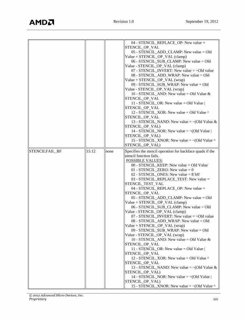
Revision 1.0 September 19, 2012
© 2012 Advanced Micro Devices, Inc. Proprietary 221
04 - STENCIL_REPLACE_OP: New value =
STENCIL_OP_VAL
05 - STENCIL_ADD_CLAMP: New value = Old
Value + STENCIL_OP_VAL (clamp)
06 - STENCIL_SUB_CLAMP: New value = Old
Value - STENCIL_OP_VAL (clamp)
07 - STENCIL_INVERT: New value = ~Old value
08 - STENCIL_ADD_WRAP: New value = Old
Value + STENCIL_OP_VAL (wrap)
09 - STENCIL_SUB_WRAP: New value = Old
Value - STENCIL_OP_VAL (wrap)
10 - STENCIL_AND: New value = Old Value &
STENCIL_OP_VAL
11 - STENCIL_OR: New value = Old Value |
STENCIL_OP_VAL
12 - STENCIL_XOR: New value = Old Value ^
STENCIL_OP_VAL
13 - STENCIL_NAND: New value = ~(Old Value &
STENCIL_OP_VAL)
14 - STENCIL_NOR: New value = ~(Old Value |
STENCIL_OP_VAL)
15 - STENCIL_XNOR: New value = ~(Old Value ^
STENCIL_OP_VAL)
STENCILFAIL_BF 15:12 none Specifies the stencil operation for backface quads if the
stencil function fails.
POSSIBLE VALUES:
00 - STENCIL_KEEP: New value = Old Value
01 - STENCIL_ZERO: New value = 0
02 - STENCIL_ONES: New value = 8`hff
03 - STENCIL_REPLACE_TEST: New value =
STENCIL_TEST_VAL
04 - STENCIL_REPLACE_OP: New value =
STENCIL_OP_VAL
05 - STENCIL_ADD_CLAMP: New value = Old
Value + STENCIL_OP_VAL (clamp)
06 - STENCIL_SUB_CLAMP: New value = Old
Value - STENCIL_OP_VAL (clamp)
07 - STENCIL_INVERT: New value = ~Old value
08 - STENCIL_ADD_WRAP: New value = Old
Value + STENCIL_OP_VAL (wrap)
09 - STENCIL_SUB_WRAP: New value = Old
Value - STENCIL_OP_VAL (wrap)
10 - STENCIL_AND: New value = Old Value &
STENCIL_OP_VAL
11 - STENCIL_OR: New value = Old Value |
STENCIL_OP_VAL
12 - STENCIL_XOR: New value = Old Value ^
STENCIL_OP_VAL
13 - STENCIL_NAND: New value = ~(Old Value &
STENCIL_OP_VAL)
14 - STENCIL_NOR: New value = ~(Old Value |
STENCIL_OP_VAL)
15 - STENCIL_XNOR: New value = ~(Old Value ^

Revision 1.0 September 19, 2012
© 2012 Advanced Micro Devices, Inc. Proprietary 222
STENCIL_OP_VAL)
STENCILZPASS_BF 19:16 none Specifies the stencil operation for backface quads if the
stencil and depth functions both pass.
POSSIBLE VALUES:
00 - STENCIL_KEEP: New value = Old Value
01 - STENCIL_ZERO: New value = 0
02 - STENCIL_ONES: New value = 8`hff
03 - STENCIL_REPLACE_TEST: New value =
STENCIL_TEST_VAL
04 - STENCIL_REPLACE_OP: New value =
STENCIL_OP_VAL
05 - STENCIL_ADD_CLAMP: New value = Old
Value + STENCIL_OP_VAL (clamp)
06 - STENCIL_SUB_CLAMP: New value = Old
Value - STENCIL_OP_VAL (clamp)
07 - STENCIL_INVERT: New value = ~Old value
08 - STENCIL_ADD_WRAP: New value = Old
Value + STENCIL_OP_VAL (wrap)
09 - STENCIL_SUB_WRAP: New value = Old
Value - STENCIL_OP_VAL (wrap)
10 - STENCIL_AND: New value = Old Value &
STENCIL_OP_VAL
11 - STENCIL_OR: New value = Old Value |
STENCIL_OP_VAL
12 - STENCIL_XOR: New value = Old Value ^
STENCIL_OP_VAL
13 - STENCIL_NAND: New value = ~(Old Value &
STENCIL_OP_VAL)
14 - STENCIL_NOR: New value = ~(Old Value |
STENCIL_OP_VAL)
15 - STENCIL_XNOR: New value = ~(Old Value ^
STENCIL_OP_VAL)
STENCILZFAIL_BF 23:20 none Specifies the stencil operation for backface quads if the
stencil function passes and the depth function fails.
POSSIBLE VALUES:
00 - STENCIL_KEEP: New value = Old Value
01 - STENCIL_ZERO: New value = 0
02 - STENCIL_ONES: New value = 8`hff
03 - STENCIL_REPLACE_TEST: New value =
STENCIL_TEST_VAL
04 - STENCIL_REPLACE_OP: New value =
STENCIL_OP_VAL
05 - STENCIL_ADD_CLAMP: New value = Old
Value + STENCIL_OP_VAL (clamp)
06 - STENCIL_SUB_CLAMP: New value = Old
Value - STENCIL_OP_VAL (clamp)
07 - STENCIL_INVERT: New value = ~Old value
08 - STENCIL_ADD_WRAP: New value = Old
Value + STENCIL_OP_VAL (wrap)
09 - STENCIL_SUB_WRAP: New value = Old
Value - STENCIL_OP_VAL (wrap)
10 - STENCIL_AND: New value = Old Value &

Revision 1.0 September 19, 2012
© 2012 Advanced Micro Devices, Inc. Proprietary 223
STENCIL_OP_VAL
11 - STENCIL_OR: New value = Old Value |
STENCIL_OP_VAL
12 - STENCIL_XOR: New value = Old Value ^
STENCIL_OP_VAL
13 - STENCIL_NAND: New value = ~(Old Value &
STENCIL_OP_VAL)
14 - STENCIL_NOR: New value = ~(Old Value |
STENCIL_OP_VAL)
15 - STENCIL_XNOR: New value = ~(Old Value ^
STENCIL_OP_VAL)
DB:DB_STENCIL_INFO · [R/W] · 32 bits · Access: 32 · GpuF0MMReg:0x28044
Field Name Bits Default Description
FORMAT 0 none Specifies the size of the Stencil component.
POSSIBLE VALUES:
00 - STENCIL_INVALID: Invalid stencil surface.
01 - STENCIL_8: 8-bit INT stencil surface.
TILE_SPLIT 15:13 none Specifies the number of bytes that will be stored
contiguously for each tile. If the tile data requires more
storage than this amount, it is split into multiple slices.
This field must not be larger than
GB_ADDR_CONFIG.DRAM_ROW_SIZE. Only applies
to 2D tiling modes.
POSSIBLE VALUES:
00 - ADDR_SURF_TILE_SPLIT_64B:
01 - ADDR_SURF_TILE_SPLIT_128B:
02 - ADDR_SURF_TILE_SPLIT_256B:
03 - ADDR_SURF_TILE_SPLIT_512B:
04 - ADDR_SURF_TILE_SPLIT_1KB:
05 - ADDR_SURF_TILE_SPLIT_2KB:
06 - ADDR_SURF_TILE_SPLIT_4KB:
ALLOW_EXPCLEAR 27 none Allow Stencil Memory Format to keep track of expanded
and clear.
TILE_STENCIL_DISABLE 29 none Indicates that htile buffer has no stencil metadata. This
improves hiz precision at the cost of having no stencil
compression or HiStencil optimizations.
DB:DB_STENCIL_READ_BASE · [R/W] · 32 bits · Access: 32 · GpuF0MMReg:0x2804c
Field Name Bits Default Description
BASE_256B 31:0 none Location of the first byte of the Stencil surface for READ
in Device Address Space, which must be 256 byte
aligned. High 32-bits of 40-bit address.
DB:DB_STENCIL_WRITE_BASE · [R/W] · 32 bits · Access: 32 · GpuF0MMReg:0x28054
Field Name Bits Default Description
BASE_256B 31:0 none Location of the first byte of the Stencil surface for
WRITE in Device Address Space, which must be 256

Revision 1.0 September 19, 2012
© 2012 Advanced Micro Devices, Inc. Proprietary 224
byte aligned. High 32-bits of 40-bit address.
DB:DB_SUBTILE_CONTROL · [R/W] · 32 bits · Access: 32 · GpuF0MMReg:0x9858
DESCRIPTION: Controls subtile X and Y size for each MSAA level, for a squad`s size to a full tile
Field Name Bits Default Description
MSAA1_X 1:0 0x0 1xMSAA squad is 4x4 : auto, 4, 4, 8 (2 not allowed since
< a squad in X)
MSAA1_Y 3:2 0x0 1xMSAA squad is 4x4 : auto, 4, 4, 8 (2 not allowed since
< a squad in Y)
MSAA2_X 5:4 0x0 2xMSAA squad is 4x2 : auto, 4, 4, 8 (2 not allowed since
< a squad in X)
MSAA2_Y 7:6 0x0 2xMSAA squad is 4x2 : auto, 2, 4, 8
MSAA4_X 9:8 0x0 4xMSAA squad is 2x2 : auto, 2, 4, 8
MSAA4_Y 11:10 0x0 4xMSAA squad is 2x2 : auto, 2, 4, 8
MSAA8_X 13:12 0x0 8xMSAA squad is 2x1 : auto, 2, 4, 8
MSAA8_Y 15:14 0x0 8xMSAA squad is 2x1 : auto, 2, 4, 8 (1 not allowed since
want a mininum of a full quad)
MSAA16_X 17:16 0x0
MSAA16_Y 19:18 0x0
DB:DB_Z_INFO · [R/W] · 32 bits · Access: 32 · GpuF0MMReg:0x28040
Field Name Bits Default Description
FORMAT 1:0 none Specifies the size of the depth component and whether
depth is floating point.
POSSIBLE VALUES:
00 - Z_INVALID: Invalid depth surface.
01 - Z_16: 16-bit UNORM depth surface.
03 - Z_32_FLOAT: 32-bit FLOAT depth surface.
NUM_SAMPLES 3:2 none Specifies the MSAA surface footprint of the Z surface.
TILE_SPLIT 15:13 none Specifies the number of bytes that will be stored
contiguously for each tile. If the tile data requires more
storage than this amount, it is split into multiple slices.
This field must not be larger than
GB_ADDR_CONFIG.DRAM_ROW_SIZE. Only applies
to 2D tiling modes.
POSSIBLE VALUES:
00 - ADDR_SURF_TILE_SPLIT_64B:
01 - ADDR_SURF_TILE_SPLIT_128B:
02 - ADDR_SURF_TILE_SPLIT_256B:
03 - ADDR_SURF_TILE_SPLIT_512B:
04 - ADDR_SURF_TILE_SPLIT_1KB:
05 - ADDR_SURF_TILE_SPLIT_2KB:
06 - ADDR_SURF_TILE_SPLIT_4KB:
ALLOW_EXPCLEAR 27 none Allow ZMask to keep track of expanded and clear.
READ_SIZE 28 none Sets the minimum size for reads to be 512 bits. Set if the
surface is in a memory pool that has granularity penalty

Revision 1.0 September 19, 2012
© 2012 Advanced Micro Devices, Inc. Proprietary 225
with < 512 bit accesses.
POSSIBLE VALUES:
00 - READ_256_BITS
01 - READ_512_BITS
TILE_SURFACE_ENABLE 29 none Enables reading and writing of the htile data. If off
HiZ+S is off.
ZRANGE_PRECISION 31 none 0 = ZMin is the base, generally set when doing a Z > test,
1 = ZMax is the base, set when generally using a Z < test.
The value used as base has full 14 bit precision. By
setting the base to Max culling has less error in a < test.
Can only be changed after a full surface clear. This field
is only meaningful if TILE_Z_ONLY == 0
DB:DB_Z_READ_BASE · [R/W] · 32 bits · Access: 32 · GpuF0MMReg:0x28048
Field Name Bits Default Description
BASE_256B 31:0 none Location of the first byte of the Z surface for READ in
Device Address Space, which must be 256 byte aligned.
High 32-bits of 40-bit address.
DB:DB_Z_WRITE_BASE · [R/W] · 32 bits · Access: 32 · GpuF0MMReg:0x28050
Field Name Bits Default Description
BASE_256B 31:0 none Location of the first byte of the Z surface for WRITE in
Device Address Space, which must be 256 byte aligned.
High 32-bits of 40-bit address.
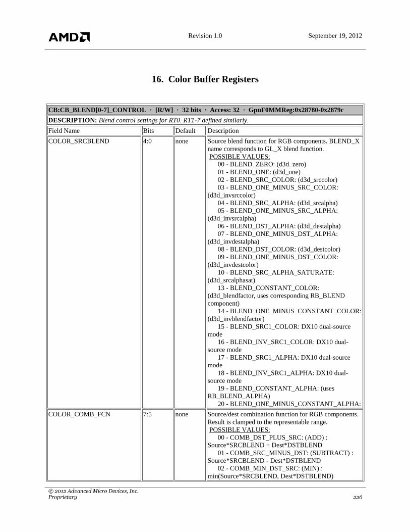
Revision 1.0 September 19, 2012
© 2012 Advanced Micro Devices, Inc. Proprietary 226
16. Color Buffer Registers
CB:CB_BLEND[0-7]_CONTROL · [R/W] · 32 bits · Access: 32 · GpuF0MMReg:0x28780-0x2879c
DESCRIPTION: Blend control settings for RT0. RT1-7 defined similarly.
Field Name Bits Default Description
COLOR_SRCBLEND 4:0 none Source blend function for RGB components. BLEND_X
name corresponds to GL_X blend function.
POSSIBLE VALUES:
00 - BLEND_ZERO: (d3d_zero)
01 - BLEND_ONE: (d3d_one)
02 - BLEND_SRC_COLOR: (d3d_srccolor)
03 - BLEND_ONE_MINUS_SRC_COLOR:
(d3d_invsrccolor)
04 - BLEND_SRC_ALPHA: (d3d_srcalpha)
05 - BLEND_ONE_MINUS_SRC_ALPHA:
(d3d_invsrcalpha)
06 - BLEND_DST_ALPHA: (d3d_destalpha)
07 - BLEND_ONE_MINUS_DST_ALPHA:
(d3d_invdestalpha)
08 - BLEND_DST_COLOR: (d3d_destcolor)
09 - BLEND_ONE_MINUS_DST_COLOR:
(d3d_invdestcolor)
10 - BLEND_SRC_ALPHA_SATURATE:
(d3d_srcalphasat)
13 - BLEND_CONSTANT_COLOR:
(d3d_blendfactor, uses corresponding RB_BLEND
component)
14 - BLEND_ONE_MINUS_CONSTANT_COLOR:
(d3d_invblendfactor)
15 - BLEND_SRC1_COLOR: DX10 dual-source
mode
16 - BLEND_INV_SRC1_COLOR: DX10 dual-
source mode
17 - BLEND_SRC1_ALPHA: DX10 dual-source
mode
18 - BLEND_INV_SRC1_ALPHA: DX10 dual-
source mode
19 - BLEND_CONSTANT_ALPHA: (uses
RB_BLEND_ALPHA)
20 - BLEND_ONE_MINUS_CONSTANT_ALPHA:
COLOR_COMB_FCN 7:5 none Source/dest combination function for RGB components.
Result is clamped to the representable range.
POSSIBLE VALUES:
00 - COMB_DST_PLUS_SRC: (ADD) :
Source*SRCBLEND + Dest*DSTBLEND
01 - COMB_SRC_MINUS_DST: (SUBTRACT) :
Source*SRCBLEND - Dest*DSTBLEND
02 - COMB_MIN_DST_SRC: (MIN) :
min(Source*SRCBLEND, Dest*DSTBLEND)

Revision 1.0 September 19, 2012
© 2012 Advanced Micro Devices, Inc. Proprietary 227
03 - COMB_MAX_DST_SRC: (MAX) :
max(Source*SRCBLEND, Dest*DSTBLEND)
04 - COMB_DST_MINUS_SRC:
(REVSUBTRACT): Dest*DSTBLEND -
Source*SRCBLEND
COLOR_DESTBLEND 12:8 none Destination blend function for RGB components.
BLEND_X name corresponds to GL_X blend function.
POSSIBLE VALUES:
00 - BLEND_ZERO: (d3d_zero)
01 - BLEND_ONE: (d3d_one)
02 - BLEND_SRC_COLOR: (d3d_srccolor)
03 - BLEND_ONE_MINUS_SRC_COLOR:
(d3d_invsrccolor)
04 - BLEND_SRC_ALPHA: (d3d_srcalpha)
05 - BLEND_ONE_MINUS_SRC_ALPHA:
(d3d_invsrcalpha)
06 - BLEND_DST_ALPHA: (d3d_destalpha)
07 - BLEND_ONE_MINUS_DST_ALPHA:
(d3d_invdestalpha)
08 - BLEND_DST_COLOR: (d3d_destcolor)
09 - BLEND_ONE_MINUS_DST_COLOR:
(d3d_invdestcolor)
10 - BLEND_SRC_ALPHA_SATURATE:
(d3d_srcalphasat)
13 - BLEND_CONSTANT_COLOR:
(d3d_blendfactor, uses corresponding RB_BLEND
component)
14 - BLEND_ONE_MINUS_CONSTANT_COLOR:
(d3d_invblendfactor)
15 - BLEND_SRC1_COLOR: DX10 dual-source
mode
16 - BLEND_INV_SRC1_COLOR: DX10 dual-
source mode
17 - BLEND_SRC1_ALPHA: DX10 dual-source
mode
18 - BLEND_INV_SRC1_ALPHA: DX10 dual-
source mode
19 - BLEND_CONSTANT_ALPHA: (uses
RB_BLEND_ALPHA)
20 - BLEND_ONE_MINUS_CONSTANT_ALPHA:
ALPHA_SRCBLEND 20:16 none Source blend function for alpha component. BLEND_X
name corresponds to GL_X blend function.
POSSIBLE VALUES:
00 - BLEND_ZERO: (d3d_zero)
01 - BLEND_ONE: (d3d_one)
02 - BLEND_SRC_COLOR: (d3d_srccolor)
03 - BLEND_ONE_MINUS_SRC_COLOR:
(d3d_invsrccolor)
04 - BLEND_SRC_ALPHA: (d3d_srcalpha)
05 - BLEND_ONE_MINUS_SRC_ALPHA:
(d3d_invsrcalpha)
06 - BLEND_DST_ALPHA: (d3d_destalpha)
07 - BLEND_ONE_MINUS_DST_ALPHA:
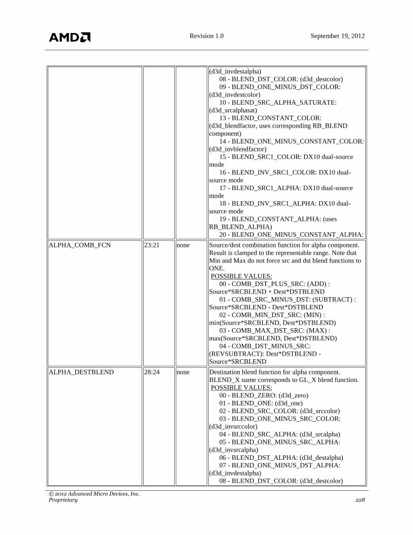
Revision 1.0 September 19, 2012
© 2012 Advanced Micro Devices, Inc. Proprietary 228
(d3d_invdestalpha)
08 - BLEND_DST_COLOR: (d3d_destcolor)
09 - BLEND_ONE_MINUS_DST_COLOR:
(d3d_invdestcolor)
10 - BLEND_SRC_ALPHA_SATURATE:
(d3d_srcalphasat)
13 - BLEND_CONSTANT_COLOR:
(d3d_blendfactor, uses corresponding RB_BLEND
component)
14 - BLEND_ONE_MINUS_CONSTANT_COLOR:
(d3d_invblendfactor)
15 - BLEND_SRC1_COLOR: DX10 dual-source
mode
16 - BLEND_INV_SRC1_COLOR: DX10 dual-
source mode
17 - BLEND_SRC1_ALPHA: DX10 dual-source
mode
18 - BLEND_INV_SRC1_ALPHA: DX10 dual-
source mode
19 - BLEND_CONSTANT_ALPHA: (uses
RB_BLEND_ALPHA)
20 - BLEND_ONE_MINUS_CONSTANT_ALPHA:
ALPHA_COMB_FCN 23:21 none Source/dest combination function for alpha component.
Result is clamped to the representable range. Note that
Min and Max do not force src and dst blend functions to
ONE.
POSSIBLE VALUES:
00 - COMB_DST_PLUS_SRC: (ADD) :
Source*SRCBLEND + Dest*DSTBLEND
01 - COMB_SRC_MINUS_DST: (SUBTRACT) :
Source*SRCBLEND - Dest*DSTBLEND
02 - COMB_MIN_DST_SRC: (MIN) :
min(Source*SRCBLEND, Dest*DSTBLEND)
03 - COMB_MAX_DST_SRC: (MAX) :
max(Source*SRCBLEND, Dest*DSTBLEND)
04 - COMB_DST_MINUS_SRC:
(REVSUBTRACT): Dest*DSTBLEND -
Source*SRCBLEND
ALPHA_DESTBLEND 28:24 none Destination blend function for alpha component.
BLEND_X name corresponds to GL_X blend function.
POSSIBLE VALUES:
00 - BLEND_ZERO: (d3d_zero)
01 - BLEND_ONE: (d3d_one)
02 - BLEND_SRC_COLOR: (d3d_srccolor)
03 - BLEND_ONE_MINUS_SRC_COLOR:
(d3d_invsrccolor)
04 - BLEND_SRC_ALPHA: (d3d_srcalpha)
05 - BLEND_ONE_MINUS_SRC_ALPHA:
(d3d_invsrcalpha)
06 - BLEND_DST_ALPHA: (d3d_destalpha)
07 - BLEND_ONE_MINUS_DST_ALPHA:
(d3d_invdestalpha)
08 - BLEND_DST_COLOR: (d3d_destcolor)

Revision 1.0 September 19, 2012
© 2012 Advanced Micro Devices, Inc. Proprietary 229
09 - BLEND_ONE_MINUS_DST_COLOR:
(d3d_invdestcolor)
10 - BLEND_SRC_ALPHA_SATURATE:
(d3d_srcalphasat)
13 - BLEND_CONSTANT_COLOR:
(d3d_blendfactor, uses corresponding RB_BLEND
component)
14 - BLEND_ONE_MINUS_CONSTANT_COLOR:
(d3d_invblendfactor)
15 - BLEND_SRC1_COLOR: DX10 dual-source
mode
16 - BLEND_INV_SRC1_COLOR: DX10 dual-
source mode
17 - BLEND_SRC1_ALPHA: DX10 dual-source
mode
18 - BLEND_INV_SRC1_ALPHA: DX10 dual-
source mode
19 - BLEND_CONSTANT_ALPHA: (uses
RB_BLEND_ALPHA)
20 - BLEND_ONE_MINUS_CONSTANT_ALPHA:
SEPARATE_ALPHA_BLEND 29 none If false, use color blend modes for blending the alpha
channel. If true, use the ALPHA_ fields to control
blending to the alpha channel.
ENABLE 30 none 1=Enables blending for this MRT, 0=Disables blending
for this MRT. if Blending is enabled then it overrides and
disables ROP3.
DISABLE_ROP3 31 0x0 (DEFAULT) 0=Enables ROP3 for this MRT, 1=Disable
ROP3 for this MRT. If enabled,
CB_COLOR_CONTROL.ROP3 is used to perform ROP
operation. If Blending is enabled then ROP3 is
overridden and disabled
CB:CB_BLEND_ALPHA · [R/W] · 32 bits · Access: 32 · GpuF0MMReg:0x28420
DESCRIPTION: Blend color constant.
Field Name Bits Default Description
BLEND_ALPHA 31:0 none FP32 alpha component of constant blend color.
CB:CB_BLEND_BLUE · [R/W] · 32 bits · Access: 32 · GpuF0MMReg:0x2841c
DESCRIPTION: Blend color constant.
Field Name Bits Default Description
BLEND_BLUE 31:0 none FP32 blue component of constant blend color.
CB:CB_BLEND_GREEN · [R/W] · 32 bits · Access: 32 · GpuF0MMReg:0x28418
DESCRIPTION: Blend color constant.
Field Name Bits Default Description
BLEND_GREEN 31:0 none FP32 green component of constant blend color.

Revision 1.0 September 19, 2012
© 2012 Advanced Micro Devices, Inc. Proprietary 230
CB:CB_BLEND_RED · [R/W] · 32 bits · Access: 32 · GpuF0MMReg:0x28414
DESCRIPTION: Blend color constant.
Field Name Bits Default Description
BLEND_RED 31:0 none FP32 red component of constant blend color.
CB:CB_COLOR[0-7]_ATTRIB · [R/W] · 32 bits · Access: 32 · GpuF0MMReg:0x28c74-0x28e18
DESCRIPTION: Surface address information for RT0. RT1-7 defined similarly.
Field Name Bits Default Description
TILE_MODE_INDEX 4:0 none Index used to lookup GB_TILE_MODEn register for
COLOR and CMASK surface tiling settings.
FMASK_TILE_MODE_INDEX 9:5 none Index used to lookup GB_TILE_MODEn register for
FMASK surface tiling settings.
NUM_SAMPLES 14:12 none Specifies log2 of the number of samples. This cannot be
greater than 4 (i.e 16 samples )
NUM_FRAGMENTS 16:15 none Specifies log2 of the number of fragments. This cannot be
greater than MIN(NUM_SAMPLES, 3) since log2(3) ==
8 fragments
FORCE_DST_ALPHA_1 17 none If set, forces DST_ALPHA=1.0f .
Mainly used with COLOR_8_8_8_8 format but can be
used with any format/comp_swap combination that has
an alpha component.
The main usage of this bit is for applications that only
request color components but gets a format with alpha as
well. Usually for format/comp_swap combinations that
don`t have alpha then alpha is assumed to be 1.0f.
Similarly, if an application gets a format/comp_swap
combo with alpha but didn`t request it then setting this bit
forces DST ALPHA=1.0f.
CB:CB_COLOR[0-7]_BASE · [R/W] · 32 bits · Access: 32 · GpuF0MMReg:0x28c60-0x28e04
DESCRIPTION: Base address for COLOR surface for RT0. RT1-7 defined similarly.
Field Name Bits Default Description
BASE_256B 31:0 none This specifies bits [39:8] of the byte address of the start
of the resource in device address space.
LINEAR GENERAL surface: bits [7:0] of the byte
address are specified in
CB_COLOR0_VIEW.SLICE_START.
NON-LINEAR GENERAL surfaces: bits [7:0] of the
byte address are always zero.
CB:CB_COLOR[0-7]_CLEAR_WORD0 · [R/W] · 32 bits · Access: 32 · GpuF0MMReg:0x28c8c-0x28e30
DESCRIPTION: Bits [31:0] of the per-MRT formatted fast clear color. Pixel size Clear color 8bpp WORD0[7:0]
16bpp WORD0[15:0] 32bpp WORD0[31:0] 64bpp {WORD1[31:0], WORD0[31:0]} 128bpp Unsupported
Field Name Bits Default Description
CLEAR_WORD0 31:0 none

Revision 1.0 September 19, 2012
© 2012 Advanced Micro Devices, Inc. Proprietary 231
CB:CB_COLOR[0-7]_CLEAR_WORD1 · [R/W] · 32 bits · Access: 32 · GpuF0MMReg:0x28c90-
0x28e34
DESCRIPTION: Bits [63:32] of the per-MRT formatted fast clear color. Pixel size Clear color 8bpp WORD0[7:0]
16bpp WORD0[15:0] 32bpp WORD0[31:0] 64bpp {WORD1[31:0], WORD0[31:0]} 128bpp Unsupported
Field Name Bits Default Description
CLEAR_WORD1 31:0 none
CB:CB_COLOR[0-7]_CMASK · [R/W] · 32 bits · Access: 32 · GpuF0MMReg:0x28c7c-0x28e20
DESCRIPTION: Base address for CMASK surface for RT0. RT1-7 defined similarly.
Field Name Bits Default Description
BASE_256B 31:0 none This specifies bits [39:8] of the byte address of the start
of the per-tile CMASK data, if any, in device address
space.
CB:CB_COLOR[0-7]_CMASK_SLICE · [R/W] · 32 bits · Access: 32 · GpuF0MMReg:0x28c80-0x28e24
DESCRIPTION: Size of CMASK surface slice for RT0. RT1-7 defined similarly
Field Name Bits Default Description
TILE_MAX 13:0 none Encodes the size of a slice. This field equals one less
than the number of 128x128 blocks (16x16 tiles) of
CMASK data per slice.
CB:CB_COLOR[0-7]_FMASK · [R/W] · 32 bits · Access: 32 · GpuF0MMReg:0x28c84-0x28e28
DESCRIPTION: Base address for FMASK surface for RT0. RT1-7 defined similarly.
Field Name Bits Default Description
BASE_256B 31:0 none This specifies bits [39:8] of the byte address of the start
of the resource in device address space.
CB:CB_COLOR[0-7]_FMASK_SLICE · [R/W] · 32 bits · Access: 32 · GpuF0MMReg:0x28c88-0x28e2c
DESCRIPTION: Size of FMASK surface slice for RT0. RT1-7 defined similarly.
Field Name Bits Default Description
TILE_MAX 21:0 none Encodes the size of a slice. This field equals one less
than the number of 8x8 tiles of FMASK data per slice.
CB:CB_COLOR[0-7]_INFO · [R/W] · 32 bits · Access: 32 · GpuF0MMReg:0x28c70-0x28e14
DESCRIPTION: COLOR Surface format information for RT0. RT1-7 defined similarly.
Field Name Bits Defa
ult Description
ENDIAN 1:0 none Specifies what kind of byte swapping to perform, if any, for different
endian modes. The byte swap is equivalent to computing dest[A] = src[A
XOR N] for byte address A and the XOR values listed below. See the
COMP_SWAP field for component swapping options.
POSSIBLE VALUES:
00 - ENDIAN_NONE: No endian swapping (XOR by 0)
01 - ENDIAN_8IN16: 8 bit swap within 16 bit word
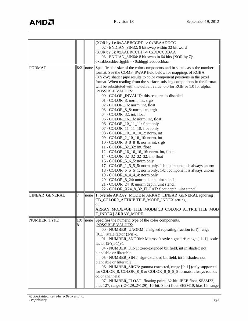
Revision 1.0 September 19, 2012
© 2012 Advanced Micro Devices, Inc. Proprietary 232
(XOR by 1): 0xAABBCCDD -> 0xBBAADDCC
02 - ENDIAN_8IN32: 8 bit swap within 32 bit word
(XOR by 3): 0xAABBCCDD -> 0xDDCCBBAA
03 - ENDIAN_8IN64: 8 bit swap in 64 bits (XOR by 7):
0xaabbccddeeffgghh -> 0xhhggffeeddccbbaa
FORMAT 6:2 none Specifies the size of the color components and in some cases the number
format. See the COMP_SWAP field below for mappings of RGBA
(XYZW) shader pipe results to color component positions in the pixel
format. When reading from the surface, missing components in the format
will be substituted with the default value: 0.0 for RGB or 1.0 for alpha.
POSSIBLE VALUES:
00 - COLOR_INVALID: this resource is disabled
01 - COLOR_8: norm, int, srgb
02 - COLOR_16: norm, int, float
03 - COLOR_8_8: norm, int, srgb
04 - COLOR_32: int, float
05 - COLOR_16_16: norm, int, float
06 - COLOR_10_11_11: float only
07 - COLOR_11_11_10: float only
08 - COLOR_10_10_10_2: norm, int
09 - COLOR_2_10_10_10: norm, int
10 - COLOR_8_8_8_8: norm, int, srgb
11 - COLOR_32_32: int, float
12 - COLOR_16_16_16_16: norm, int, float
14 - COLOR_32_32_32_32: int, float
16 - COLOR_5_6_5: norm only
17 - COLOR_1_5_5_5: norm only, 1-bit component is always unorm
18 - COLOR_5_5_5_1: norm only, 1-bit component is always unorm
19 - COLOR_4_4_4_4: norm only
20 - COLOR_8_24: unorm depth, uint stencil
21 - COLOR_24_8: unorm depth, uint stencil
22 - COLOR_X24_8_32_FLOAT: float depth, uint stencil
LINEAR_GENERAL 7 none 1: overide ARRAY_MODE to ARRAY_LINEAR_GENERAL ignoring
CB_COLOR0_ATTRIB.TILE_MODE_INDEX setting.
0:
ARRAY_MODE=GB_TILE_MODE[CB_COLOR0_ATTRIB.TILE_MOD
E_INDEX].ARRAY_MODE
NUMBER_TYPE 10:
8
none Specifies the numeric type of the color components.
POSSIBLE VALUES:
00 - NUMBER_UNORM: unsigned repeating fraction (urf): range
[0..1], scale factor (2^n)-1
01 - NUMBER_SNORM: Microsoft-style signed rf: range [-1..1], scale
factor (2^(n-1))-1
04 - NUMBER_UINT: zero-extended bit field, int in shader: not
blendable or filterable
05 - NUMBER_SINT: sign-extended bit field, int in shader: not
blendable or filterable
06 - NUMBER_SRGB: gamma corrected, range [0..1] (only supported
for COLOR_8, COLOR_8_8 or COLOR_8_8_8_8 formats; always rounds
color channels)
07 - NUMBER_FLOAT: floating point: 32-bit: IEEE float, SE8M23,
bias 127, range (-2^129..2^129); 16-bit: Short float SE5M10, bias 15, range

Revision 1.0 September 19, 2012
© 2012 Advanced Micro Devices, Inc. Proprietary 233
(-2^17..2^17); 11-bit: Packed float, E5M6 bias 15, range [0..2^17); 10-bit:
Packed float, E5M5 bias 15, range [0..2^17)
COMP_SWAP 12:
11
none Specifies how to map the red, green, blue, and alpha components from the
shader to the components in the render target pixel format (components 0,
1, 2, 3 with 0 begin least significant, 3 begin most). With one component,
this selects which colour channel to map to the single render target
component (STD: R=>0; ALT: G=>0; STD_REV: B=>0; ALT_REV:
A=>0). With 2-4 components, SWAP_STD always maps shader
components starting with R=>0 up to the number of components available
(component R=>0, G=>1, B=>2, A=>3). With 2-3 components,
SWAP_ALT mimics SWAP_STD except alpha from the shader is always
sent to the last render target component (2 components: R=>0, A=>1; 3
components: R=>0, G=>1, A=>2). With 4 components, SWAP_ALT
selects an alternate order (B=>0, G=>1, R=>2, A=>3). With 2-4
components, SWAP_STD_REV and SWAP_ALT_REV reverse the
component order.
POSSIBLE VALUES:
00 - SWAP_STD: standard little-endian comp order
01 - SWAP_ALT: alternate components or order
02 - SWAP_STD_REV: reverses SWAP_STD order
03 - SWAP_ALT_REV: reverses SWAP_ALT order
FAST_CLEAR 13 none Enables fast clear. If set, CB recognizes the fast clear encoding in cmask
and treats the corresponding tile region as being fast cleared.
COMPRESSION 14 none Enables color compression.
BLEND_CLAMP 15 none Specifies whether to clamp source data to the format range prior to
blending, in addition to the post-blend clamp. This bit must be cleared if
BLEND_BYPASS is set. Otherwise, it must be set iff any component is
SNORM, UNORM, SRGB.
BLEND_BYPASS 16 none If false, the blender for this MRT is enabled/disabled as specified in
CB_BLENDn_CONTROL.ENABLE. If true, blending is disabled. This bit
should be set iff any component is SINT/UINT (NUMBER_TYPE = SINT,
UINT, or FORMAT = COLOR_8_24, COLOR_24_8,
COLOR_X24_8_32_FLOAT).
SIMPLE_FLOAT 17 0x0 If set, simplifies floating point processing by ignoring special values like
NaN, +/-Inf and -0.0f such that DESTBLEND*DST=0.0f if
DESTBLEND==0.0f as well as SRCBLEND*SRC=0.0f if
SRCBLEND==0.0f .
If false, floating point processing follows full IEEE rules for special values
like NaN, +/-Inf and -0.0f.
For floating point surfaces, setting this field can help enable the following
blend optimizations:
- BLEND_OPT_DONT_RD_DST
- BLEND_OPT_BYPASS
- BLEND_OPT_DISCARD_PIXEL
This bit is ignored for other component formats.
ROUND_MODE 18 none This field specifies the type of rounding used on pixel component values
when converting to the final frame buffer pixel component values. This
field setting is ignored for number types UINT and SINT with
ROUND_TRUNCATE always being selected. For pixel formats with
mixed component number types, this setting is also ignored for the minority
number type component (ROUND_BY_HALF is always used) but

Revision 1.0 September 19, 2012
© 2012 Advanced Micro Devices, Inc. Proprietary 234
applicable to the other components. Program Guidelines: set to
ROUND_BY_HALF if number type is any of (UNORM, SNORM or
SRGB) or color format is either COLOR_8_24 or COLOR_24_8;
otherwise set to ROUND_TRUNCATE.
POSSIBLE VALUES:
00 - ROUND_BY_HALF: add 1/2 lsb and then truncate
01 - ROUND_TRUNCATE: truncate only. toward zero for float,
toward negative for non-float
CMASK_IS_LINEAR 19 none If set, Cmask surface is stored linearly. This can reduce padding restrictions
on the cmask surface.
BLEND_OPT_DONT_RD
_DST
22:
20
0x0 Blend Optimization of not reading DST:
If blend function evaluates to SRCBLEND*SRC +/- 0*DST and
SRBBLEND does not need DST as well then don`t read DST.
POSSIBLE VALUES:
00 - FORCE_OPT_AUTO: (default) HW automatically detects and
enables this optimization
01 - FORCE_OPT_DISABLE: Disable optimization for this RT.
02 - FORCE_OPT_ENABLE_IF_SRC_A_0: Enable optimization only
if Src Alpha is 0.0f
03 - FORCE_OPT_ENABLE_IF_SRC_RGB_0: Enable optimization
only if Src Color components (RGB) are all 0.0f
04 - FORCE_OPT_ENABLE_IF_SRC_ARGB_0: Enable optimization
only if Src Color components (RGB) and Alpha are all 0.0f
05 - FORCE_OPT_ENABLE_IF_SRC_A_1: Enable optimization only
if Src Alpha is 1.0f
06 - FORCE_OPT_ENABLE_IF_SRC_RGB_1: Enable optimization
only if Src Color components (RGB) are all 1.0f
07 - FORCE_OPT_ENABLE_IF_SRC_ARGB_1: Enable optimization
only if Src Color components (RGB) and Alpha are all 1.0f
BLEND_OPT_DISCARD_
PIXEL
25:
23
0x0 Blend Optimization of discarding the pixel:
If blend function evaluates to 0*SRC +/- 1*DST then this becomes a NOP.
POSSIBLE VALUES:
00 - FORCE_OPT_AUTO: (default) HW automatically detects and
enables this optimization
01 - FORCE_OPT_DISABLE: Disable optimization for this RT.
02 - FORCE_OPT_ENABLE_IF_SRC_A_0: Enable optimization only
if Src Alpha is 0.0f
03 - FORCE_OPT_ENABLE_IF_SRC_RGB_0: Enable optimization
only if Src Color components (RGB) are all 0.0f
04 - FORCE_OPT_ENABLE_IF_SRC_ARGB_0: Enable optimization
only if Src Color components (RGB) and Alpha are all 0.0f
05 - FORCE_OPT_ENABLE_IF_SRC_A_1: Enable optimization only
if Src Alpha is 1.0f
06 - FORCE_OPT_ENABLE_IF_SRC_RGB_1: Enable optimization
only if Src Color components (RGB) are all 1.0f
07 - FORCE_OPT_ENABLE_IF_SRC_ARGB_1: Enable optimization
only if Src Color components (RGB) and Alpha are all 1.0f
FMASK_COMPRESSION
_DISABLE
26 none 0=fmask compression is enabled
1=fmask compression is disabled such that fmask is always in
expanded/decompressed/resolved/non-bitplane mode.
This also means that any tile that is rendered will have its fast clear state
eliminiated.

Revision 1.0 September 19, 2012
© 2012 Advanced Micro Devices, Inc. Proprietary 235
This can be used if the MSAA buffer is to be used as a texture and it is
desired to not go through a separate FMASK_DECOMPRESS pass. This
does mean that fmask will have more memory bandwidth because it will be
always decompressed
CB:CB_COLOR[0-7]_PITCH · [R/W] · 32 bits · Access: 32 · GpuF0MMReg:0x28c64-0x28e08
DESCRIPTION: Pitch of Color and Fmask surface for RT0. RT1-7 defined similarly.
Field Name Bits Default Description
TILE_MAX 10:0 none Encodes the pitch of a scanline for Color surface; if Pitch
is the number of data elements per scanline, this field is
(Pitch / 8) - 1 and is equal to the maximum 8x8 tile
number allowed in the X dimension.
FMASK_TILE_MAX 30:20 none Encodes the pitch of a scanline for Fmask surface; if
Pitch is the number of data elements per scanline, this
field is (Pitch / 8) - 1 and is equal to the maximum 8x8
tile number allowed in the X dimension.
CB:CB_COLOR[0-7]_SLICE · [R/W] · 32 bits · Access: 32 · GpuF0MMReg:0x28c68-0x28e0c
DESCRIPTION: Size of COLOR surface slice for RT0. RT1-7 defined similarly
Field Name Bits Default Description
TILE_MAX 21:0 none Encodes the size of a slice. If SliceTiles is the maximum
number of tiles in a slice (equal to Pitch * Height / 64),
this field is SliceTiles - 1 and is equal to the maximum
tile number tile number allowed in a slice.
CB:CB_COLOR[0-7]_VIEW · [R/W] · 32 bits · Access: 32 · GpuF0MMReg:0x28c6c-0x28e10
DESCRIPTION: Selects slice index range for RT0. RT1-7 defined similarly.
Field Name Bits Default Description
SLICE_START 10:0 none For ARRAY_LINEAR_GENERAL: bits [7:0] of this
field specify bits [7:0] of the byte address of the
resource. This together with
CB_COLOR*_BASE.BASE_256B specify the 40-bit
start address. The address must be element-aligned.
When using ARRAY_LINEAR_GENERAL, since there
is no actual value for SLICE_START, the
SLICE_START value is assumed to be zero when doing
rtindex (slice) clamping.
For all other surfaces, this specifies the starting slice
number for this view: this field is added to rtindex to
compute the slice to render.
SLICE_MAX 23:13 none Specifies the maximum allowed render target slice index
(rtindex) for this resource, which is one less than the total
number of slices. rtindex is clamped to SLICE_START
if this value is exceeded.
CB:CB_COLOR_CONTROL · [R/W] · 32 bits · Access: 32 · GpuF0MMReg:0x28808
DESCRIPTION: Controls general CB behaviour across all MRTs.

Revision 1.0 September 19, 2012
© 2012 Advanced Micro Devices, Inc. Proprietary 236
Field Name Bits Default Description
DEGAMMA_ENABLE 3 none If true, then each UNORM format COLOR_8_8_8_8,
COLOR_8_8 or COLOR_8 in every MRT is treated as
an SRGB format instead. This affects both normal draw
and resolve. This bit exists for compatibility with older
architectures that did not have an SRGB number type.
MODE 6:4 none This field selects standard color processing or one of
several major operation modes.
POSSIBLE VALUES:
00 - CB_DISABLE: Disables drawing to color
buffer. Causes DB to not send tiles/quads to CB. CB
itself ignores this field.
01 - CB_NORMAL: Normal rendering mode. DB
should send tiles and quads for pixel exports.
02 - CB_ELIMINATE_FAST_CLEAR: Fill fast
cleared color surface locations with clear color. DB
should send only tiles.
03 - CB_RESOLVE: Read from MRT0, average all
samples, and write to MRT1, which is one-sample. DB
should send only tiles.
05 - CB_FMASK_DECOMPRESS: Decompress the
FMASK buffer into a texture readable format. A
CB_ELIMINATE_FAST_CLEAR pass before this is
unnecessary. DB should send only tiles.
ROP3 23:16 none This field supports the 28 boolean ops that combine
either source and dest or brush and dest, with brush
provided by the shader in place of source. The code
0xCC (11001100) copies the source to the destination,
which disables the ROP function. ROP must be disabled
if any MRT enables blending.
POSSIBLE VALUES:
00 - 0x00: BLACKNESS
05 - 0x05
10 - 0x0A
15 - 0x0F
17 - 0x11: NOTSRCERASE
34 - 0x22
51 - 0x33: NOTSRCCOPY
68 - 0x44: SRCERASE
80 - 0x50
85 - 0x55: DSTINVERT
90 - 0x5A: PATINVERT
95 - 0x5F
102 - 0x66: SRCINVERT
119 - 0x77
136 - 0x88: SRCAND
153 - 0x99
160 - 0xA0
165 - 0xA5
170 - 0xAA
175 - 0xAF
187 - 0xBB: MERGEPAINT

Revision 1.0 September 19, 2012
© 2012 Advanced Micro Devices, Inc. Proprietary 237
204 - 0xCC: SRCCOPY
221 - 0xDD
238 - 0xEE: SRCPAINT
240 - 0xF0: PATCOPY
245 - 0xF5
250 - 0xFA
255 - 0xFF: WHITENESS
CB:CB_HW_CONTROL · [R/W] · 32 bits · Access: 32 · GpuF0MMReg:0x9a10
DESCRIPTION: Controls to tune the performance of this CB design and to activate functional workarounds for
various features.
Field Name Bits Default Description
CM_CACHE_EVICT_POINT 3:0 0x8
FC_CACHE_EVICT_POINT 9:6 0x8
CC_CACHE_EVICT_POINT 15:12 0x8
ALLOW_MRT_WITH_DUAL_SOURCE 16 0x0 1=Allow MRTs in
MRT#2-7 with dual-
source blending using
MRT#0-1. 0=Disable
MRT#2-7 when dual-
source blending using
MRT#0-1
DISABLE_INTNORM_LE11BPC_CLAMPING 18 0x1
FORCE_NEEDS_DST 19 0x0
FORCE_ALWAYS_TOGGLE 20 0x0
DISABLE_BLEND_OPT_RESULT_EQ_DEST 21 0x0
DISABLE_FULL_WRITE_MASK 22 0x0
DISABLE_RESOLVE_OPT_FOR_SINGLE_FRAG 23 0x0
DISABLE_BLEND_OPT_DONT_RD_DST 24 0x0
DISABLE_BLEND_OPT_BYPASS 25 0x0
DISABLE_BLEND_OPT_DISCARD_PIXEL 26 0x0
DISABLE_BLEND_OPT_WHEN_DISABLED_SRCALPHA_IS_USED 27 0x0
PRIORITIZE_FC_WR_OVER_FC_RD_ON_CMASK_CONFLICT 28 0x0
PRIORITIZE_FC_EVICT_OVER_FOP_RD_ON_BANK_CONFLICT 29 0x0
DISABLE_CC_IB_SERIALIZER_STATE_OPT 30 0x0
DISABLE_PIXEL_IN_QUAD_FIX_FOR_LINEAR_SURFACE 31 0x0
CB:CB_SHADER_MASK · [R/W] · 32 bits · Access: 32 · GpuF0MMReg:0x2823c
DESCRIPTION: Contains color component mask fields for the colors output by the shader. The bits in
OUTPUT*_ENABLE are in the same order as for TARGET*_ENABLE. Outputs 1-7 are defined equivalently to
output 0.
Field Name Bits Default Description
OUTPUT0_ENABLE 3:0 none If zero, this field disables RT 0, else it specifies which
components are enabled in the shader. The low order bit
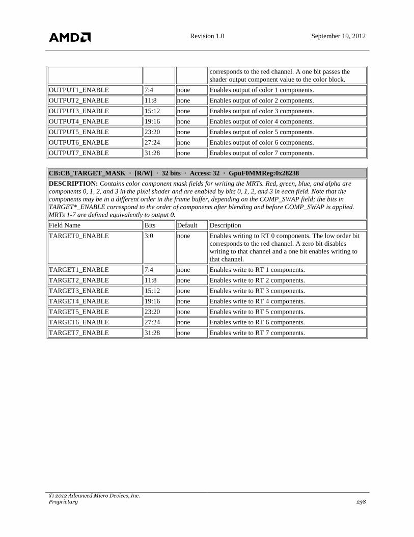
Revision 1.0 September 19, 2012
© 2012 Advanced Micro Devices, Inc. Proprietary 238
corresponds to the red channel. A one bit passes the
shader output component value to the color block.
OUTPUT1_ENABLE 7:4 none Enables output of color 1 components.
OUTPUT2_ENABLE 11:8 none Enables output of color 2 components.
OUTPUT3_ENABLE 15:12 none Enables output of color 3 components.
OUTPUT4_ENABLE 19:16 none Enables output of color 4 components.
OUTPUT5_ENABLE 23:20 none Enables output of color 5 components.
OUTPUT6_ENABLE 27:24 none Enables output of color 6 components.
OUTPUT7_ENABLE 31:28 none Enables output of color 7 components.
CB:CB_TARGET_MASK · [R/W] · 32 bits · Access: 32 · GpuF0MMReg:0x28238
DESCRIPTION: Contains color component mask fields for writing the MRTs. Red, green, blue, and alpha are
components 0, 1, 2, and 3 in the pixel shader and are enabled by bits 0, 1, 2, and 3 in each field. Note that the
components may be in a different order in the frame buffer, depending on the COMP_SWAP field; the bits in
TARGET*_ENABLE correspond to the order of components after blending and before COMP_SWAP is applied.
MRTs 1-7 are defined equivalently to output 0.
Field Name Bits Default Description
TARGET0_ENABLE 3:0 none Enables writing to RT 0 components. The low order bit
corresponds to the red channel. A zero bit disables
writing to that channel and a one bit enables writing to
that channel.
TARGET1_ENABLE 7:4 none Enables write to RT 1 components.
TARGET2_ENABLE 11:8 none Enables write to RT 2 components.
TARGET3_ENABLE 15:12 none Enables write to RT 3 components.
TARGET4_ENABLE 19:16 none Enables write to RT 4 components.
TARGET5_ENABLE 23:20 none Enables write to RT 5 components.
TARGET6_ENABLE 27:24 none Enables write to RT 6 components.
TARGET7_ENABLE 31:28 none Enables write to RT 7 components.