radeon r6xx/r7xx 3d register reference guide contents of this document are provided in connection...
TRANSCRIPT

Revision 1.0 January 26, 2009
© 2009 Advanced Micro Devices, Inc. Proprietary 1
Radeon R6xx/R7xx 3D Register
Reference Guide
Revision 1.0 January 26, 2009
© 2009 Advanced Micro Devices, Inc. Proprietary 2
Trademarks AMD, the AMD Arrow logo, Athlon, and combinations thereof, ATI, ATI logo, Radeon, and Crossfire are trademarks of Advanced Micro Devices, Inc. Microsoft and Windows are registered trademarks of Microsoft Corporation. Other product names used in this publication are for identification purposes only and may be trademarks of their respective companies. Disclaimer The contents of this document are provided in connection with Advanced Micro Devices, Inc. ("AMD") products. AMD makes no representations or warranties with respect to the accuracy or completeness of the contents of this publication and reserves the right to make changes to specifications and product descriptions at any time without notice. No license, whether express, implied, arising by estoppel, or otherwise, to any intellectual property rights are granted by this publication. Except as set forth in AMD's Standard Terms and Conditions of Sale, AMD assumes no liability whatsoever, and disclaims any express or implied warranty, relating to its products including, but not limited to, the implied warranty of merchantability, fitness for a particular purpose, or infringement of any intellectual property right. AMD's products are not designed, intended, authorized or warranted for use as components in systems intended for surgical implant into the body, or in other applications intended to support or sustain life, or in any other application in which the failure of AMD's product could create a situation where personal injury, death, or severe property or environmental damage may occur. AMD reserves the right to discontinue or make changes to its products at any time without notice. © 2009 Advanced Micro Devices, Inc. All rights reserved.
Revision 1.0 January 26, 2009
© 2009 Advanced Micro Devices, Inc. Proprietary 3
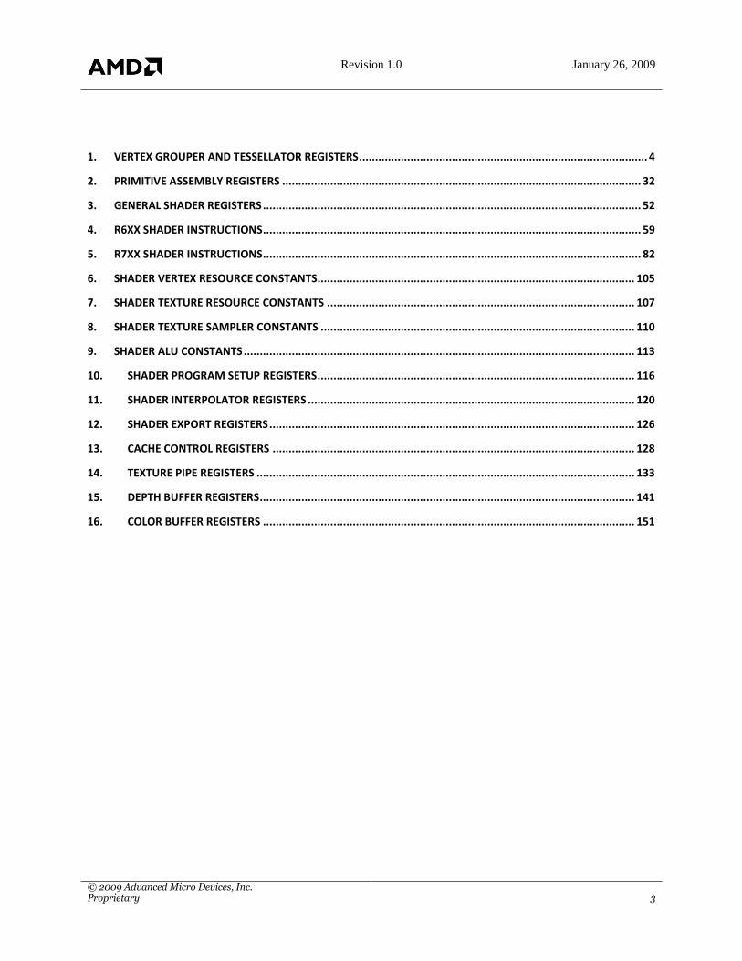
1. VERTEX GROUPER AND TESSELLATOR REGISTERS .......................................................................................... 4
2. PRIMITIVE ASSEMBLY REGISTERS ................................................................................................................ 32
3. GENERAL SHADER REGISTERS ...................................................................................................................... 52
4. R6XX SHADER INSTRUCTIONS ...................................................................................................................... 59
5. R7XX SHADER INSTRUCTIONS ...................................................................................................................... 82
6. SHADER VERTEX RESOURCE CONSTANTS................................................................................................... 105
7. SHADER TEXTURE RESOURCE CONSTANTS ................................................................................................ 107
8. SHADER TEXTURE SAMPLER CONSTANTS .................................................................................................. 110
9. SHADER ALU CONSTANTS .......................................................................................................................... 113
10. SHADER PROGRAM SETUP REGISTERS ................................................................................................... 116
11. SHADER INTERPOLATOR REGISTERS ...................................................................................................... 120
12. SHADER EXPORT REGISTERS .................................................................................................................. 126
13. CACHE CONTROL REGISTERS ................................................................................................................. 128
14. TEXTURE PIPE REGISTERS ...................................................................................................................... 133
15. DEPTH BUFFER REGISTERS ..................................................................................................................... 141
16. COLOR BUFFER REGISTERS .................................................................................................................... 151

Revision 1.0 January 26, 2009
© 2009 Advanced Micro Devices, Inc. Proprietary 4
1. Vertex Grouper and Tessellator Registers
VGT:VGT_CACHE_INVALIDATION · [R/W] · 32 bits · Access: 32 · GpuF0MMReg:0x88c4
DESCRIPTION: VGT cache invalidation
Field Name Bits Default Description
CACHE_INVALIDATION 1:0 none Indicates whether VC or TC is used for cache
invalidation
POSSIBLE VALUES:
00 - VC_ONLY: VC_ONLY
01 - TC_ONLY: TC_ONLY
02 - VC_AND_TC: VC_AND_TC
VS_NO_EXTRA_BUFFER 5 none
VGT:VGT_CNTL_STATUS · [R] · 32 bits · Access: 32 · GpuF0MMReg:0x88f0
DESCRIPTION: Status Bits
Field Name Bits Default Description
VGT_OUT_INDX_BUSY 0 none If set, the Output Index block within the VGT is busy
VGT_OUT_BUSY 1 none If set, the Output block within the VGT is busy
VGT_PT_BUSY 2 none If set, the Pass-thru block within the VGT is busy
VGT_TE_BUSY 3 none If set, the Tessellation Engine block within the VGT is
busy
VGT_VR_BUSY 4 none If set, the Vertex Reuse Block within the VGT is busy
VGT_GRP_BUSY 5 none If set, the Grouper Block within the VGT is busy
VGT_DMA_REQ_BUSY 6 none If set, the VGT DMA is busy requesting
VGT_DMA_BUSY 7 none If set, the VGT DMA is busy
VGT_GS_BUSY 8 none If set, VGT GS is actively processing
VGT_BUSY 9 none If set, VGT is Busy
VGT:VGT_DMA_BASE · [W] · 32 bits · Access: 32 · GpuF0MMReg:0x287e8
DESCRIPTION: VGT DMA Base Address
Field Name Bits Default Description
BASE_ADDR 31:0 none VGT DMA Base Address
This address must be naturally aligned to a 16-bit word.
Therefore, bit 0 of this register must be 0
VGT:VGT_DMA_BASE_HI · [W] · 32 bits · Access: 32 · GpuF0MMReg:0x287e4
DESCRIPTION: VGT DMA Base Address : upper 8-bits of 40 bit address
Field Name Bits Default Description
BASE_ADDR 7:0 none This specfies upper 8-bits of 40-bits of DMA address

Revision 1.0 January 26, 2009
© 2009 Advanced Micro Devices, Inc. Proprietary 5
VGT:VGT_DMA_INDEX_TYPE · [W] · 32 bits · Access: 32 · GpuF0MMReg:0x28a7c
DESCRIPTION: VGT DMA Index Type and Mode
Field Name Bits Default Description
INDEX_TYPE 1:0 none VGT DMA Index Type
POSSIBLE VALUES:
00 - VGT_INDEX_16: VGT_INDEX_16 16-bit
index
01 - VGT_INDEX_32: VGT_INDEX_32 32-bit
index
SWAP_MODE 3:2 none DMA Swap mode
POSSIBLE VALUES:
00 - VGT_DMA_SWAP_NONE:
VGT_DMA_SWAP_NONE No swap
01 - VGT_DMA_SWAP_16_BIT:
VGT_DMA_SWAP_16_BIT 16-bit swap
0xAABBCCDD -> 0xBBAADDCC
02 - VGT_DMA_SWAP_32_BIT:
VGT_DMA_SWAP_32_BIT 32-bit swap
0xAABBCCDD -> 0xDDCCBBAA
03 - VGT_DMA_SWAP_WORD:
VGT_DMA_SWAP_WORD word swap
0xAABBCCDD -> 0xCCDDAABB
VGT:VGT_DMA_NUM_INSTANCES · [W] · 32 bits · Access: 32 · GpuF0MMReg:0x28a88
DESCRIPTION: VGT DMA Number of Instances
Field Name Bits Default Description
NUM_INSTANCES 31:0 none VGT DMA Number of Instances, minimum value is 1
VGT:VGT_DMA_SIZE · [W] · 32 bits · Access: 32 · GpuF0MMReg:0x28a74
DESCRIPTION: VGT DMA Size
Field Name Bits Default Description
NUM_INDICES 31:0 none VGT DMA Number of indices
VGT:VGT_DRAW_INITIATOR · [W] · 32 bits · Access: 32 · GpuF0MMReg:0x287f0
DESCRIPTION: Draw Inititiator
Field Name Bits Default Description
SOURCE_SELECT 1:0 none Input Source Select.
If the Source Select field is set to `Auto-increment Index`
mode and the Primitive Type is set to `Tri List w/Flags`,

Revision 1.0 January 26, 2009
© 2009 Advanced Micro Devices, Inc. Proprietary 6
then the draw initiator is processed as just a regular `Tri
List`.
POSSIBLE VALUES:
00 - DI_SRC_SEL_DMA: VGT DMA Data
01 - DI_SRC_SEL_IMMEDIATE: Immediate Data
02 - DI_SRC_SEL_AUTO_INDEX: Auto-increment
Index
03 - DI_SRC_SEL_RESERVED: Reserved - unused
MAJOR_MODE 3:2 none Major Mode
POSSIBLE VALUES:
00 - DI_MAJOR_MODE_0: DI_MAJOR_MODE_0
Normal (Implicit) Mode -- applies only to prim types 0-
21. Some VGT state registers are ignored (their values
implied) in this mode.
01 - DI_MAJOR_MODE_1: DI_MAJOR_MODE_1
Explicit Mode -- Configuration completely specified by
state registers.
SPRITE_EN 4 none sprite enable
POSSIBLE VALUES:
00 - disable sprite
01 - enable sprite
NOT_EOP 5 none This bit indicates that this draw initiator should not
generate an end-of-packet signal because it will be
followed by one or more chained draw initiators. Care
must be taken so that this draw initiator is immediately
followed, at the hardware interface, by a chained draw
initiator. (In other words, chained draw initiators cannot
be separated over driver buffer boundaries that can be
interrupted. This bit is primarily intended to be set by the
CP to improve the processing parallelism of small 2D
blits.)
POSSIBLE VALUES:
00 - normal eop
01 - suppress eop
USE_OPAQUE 6 none This bit indicates that this draw call is a opaque draw call
POSSIBLE VALUES:
00 - non-opaque draw
01 - opaque draw
VGT:VGT_ENHANCE · [R/W] · 32 bits · Access: 32 · GpuF0MMReg:0x28a50
DESCRIPTION: Used for Late Additions of Control Bits
Field Name Bits Default Description
MI_TIMESTAMP_RES 1:0 0x0 POSSIBLE VALUES:

Revision 1.0 January 26, 2009
© 2009 Advanced Micro Devices, Inc. Proprietary 7
00 - 0 -> 992 Clocks latency range in steps of 32
01 - 0 -> 496 Clocks latency range in steps of 16
02 - 0 -> 248 Clocks latency range in steps of 8
03 - 0 -> 124 Clocks latency range in steps of 4
MISC 31:2 none Misc bit
VGT:VGT_ES_PER_GS · [R/W] · 32 bits · Access: 32 · GpuF0MMReg:0x88cc
DESCRIPTION: Maximum ES vertices per GS thread
Field Name Bits Default Description
ES_PER_GS 31:0 none Maximum number of ES vertices per GS thread
VGT:VGT_EVENT_ADDRESS_REG · [W] · 32 bits · Access: 32 · GpuF0MMReg:0x287f8
DESCRIPTION: Event address
Field Name Bits Default Description
ADDRESS_LOW 27:0 none address bit 31:4 for zpass event
VGT:VGT_EVENT_INITIATOR · [W] · 32 bits · Access: 32 · GpuF0MMReg:0x28a90
DESCRIPTION: Event Initiator
Field Name Bits Default Description
EVENT_TYPE 5:0 none Event Type (also called Event ID) -- Currently, the
hardware interface between the VGT and the PA
supports only 6-bit event type.
POSSIBLE VALUES:
00 - Reserved
01 - Reserved
02 - Reserved
03 - Reserved
04 - CACHE_FLUSH_TS: Destination Cache Flush
with Timestamp -- Inserted by the driver to request the
CBs, DBs, and SMX to signal the CP when all prior
rendering is flushed to memory.
05 - CONTEXT_DONE: GFXDEC Context Done --
Inserted by the CP on the first GFXDEC state update
after a draw.
06 - CACHE_FLUSH: Destination Caches Flushed --
Inserted by the driver to request the CBs, DBs, and SMX
to flushed their caches to memory (No Timestamp is
Generated).
07 - VIZQUERY_START: No longer supported
08 - VIZQUERY_END: No longer supported
09 - SC_WAIT_WC: SC Wait for WC from CP --
Inserted by the CP to inform the SC to wait for the write
confirm signal (wire) from the CP before submitting
future pixel vectors. This is used to synchronize 2D

Revision 1.0 January 26, 2009
© 2009 Advanced Micro Devices, Inc. Proprietary 8
source surface (brush, a.ka. texture) with user of that
surface.
10 - MPASS_PS_CP_REFETCH: Multi-Pass Pixel
Shader CP Refetch -- Inserted by the driver to inform the
SC it needs to report to CP to refetch buffer for multi-
pass pixel shader or continue.
11 - MPASS_PS_RST_START: Multi-Pass Pixel
Shader Reset Start -- Inserted by the driver just before an
INDIRECT_BUFFER_MP packet to instruct the SC to
reset the multi-pass start pixel vector.
12 - MPASS_PS_INCR_START: Multi-Pass Pixel
Shader Increment Start -- Inserted by the driver to
instruct the SC to increment the multi-pass start vector
by vectors_per_pass.
13 - RST_PIX_CNT: Reset SQ`s auto Pixel Counter
AND reset SC`s multi-pass pixel vector count -- Inserted
by the driver.
14 - RST_VTX_CNT: Reset SQ`s auto Vertex
Counter -- Inserted by the driver.
15 - VS_PARTIAL_FLUSH: Used to flush all work
between the CP and the ES, GS, VS shaders including
the VGT.
16 - PS_PARTIAL_FLUSH: Used to flush all work
between the CP and the ES, GS, VS, PS shaders
including scan conversion, primitive assembly, and
VGT.
17 - Reserved
18 - Reserved
19 - Reserved
20 - CACHE_FLUSH_AND_INV_TS_EVENT:
Same as CACHE_FLUSH_TS with an invalidate --
Inserted by the driver.
21 - ZPASS_DONE: Write ZPASS counts to
memory -- Inserted by the driver to instruct the DBs to
write out the ZPASS counters to memory. Used to
support DX10 occlusion queries.
22 - CACHE_FLUSH_AND_INV_EVENT: Same as
CACHE_FLUSH with an invalidate -- Inserted by the
driver.
23 - PERFCOUNTER_START: Start enabled event
based Performance counters -- Inserted by the driver.
24 - PERFCOUNTER_STOP: Stop enabled event
based Performance counters that are event-enabled --
Inserted by the driver.
25 - PIPELINESTAT_START: Start
pipeline/strmout stat -- Inserted by the driver.
26 - PIPELINESTAT_STOP: Stop pipeline/strmout
stat -- Inserted by the driver.
27 - PERFCOUNTER_SAMPLE: Sample the
performance counters of all blocks -- Inserted by the
driver to read the performance counters.
28 - FLUSH_ES_OUTPUT: Flush Export Shader
Output -- Inserted by the VGT to instruct the SMX to
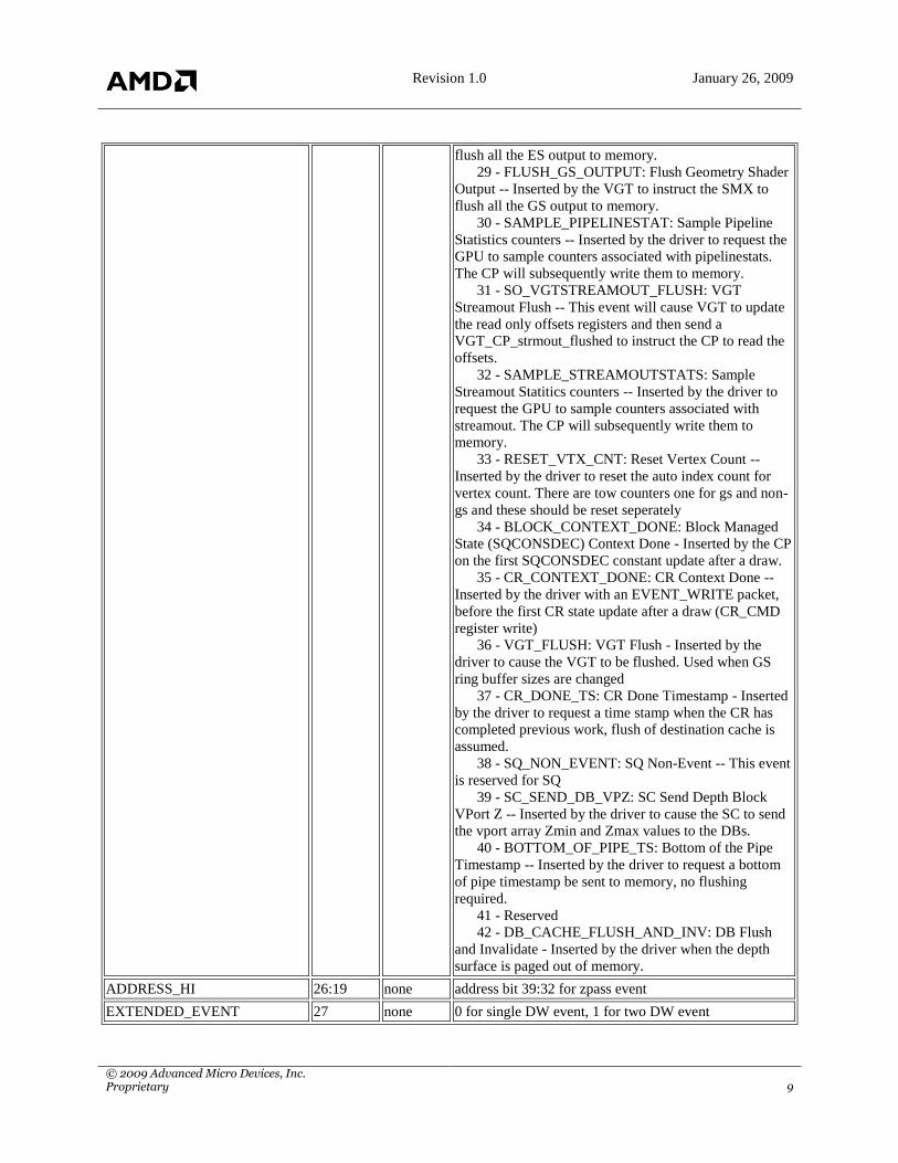
Revision 1.0 January 26, 2009
© 2009 Advanced Micro Devices, Inc. Proprietary 9
flush all the ES output to memory.
29 - FLUSH_GS_OUTPUT: Flush Geometry Shader
Output -- Inserted by the VGT to instruct the SMX to
flush all the GS output to memory.
30 - SAMPLE_PIPELINESTAT: Sample Pipeline
Statistics counters -- Inserted by the driver to request the
GPU to sample counters associated with pipelinestats.
The CP will subsequently write them to memory.
31 - SO_VGTSTREAMOUT_FLUSH: VGT
Streamout Flush -- This event will cause VGT to update
the read only offsets registers and then send a
VGT_CP_strmout_flushed to instruct the CP to read the
offsets.
32 - SAMPLE_STREAMOUTSTATS: Sample
Streamout Statitics counters -- Inserted by the driver to
request the GPU to sample counters associated with
streamout. The CP will subsequently write them to
memory.
33 - RESET_VTX_CNT: Reset Vertex Count --
Inserted by the driver to reset the auto index count for
vertex count. There are tow counters one for gs and non-
gs and these should be reset seperately
34 - BLOCK_CONTEXT_DONE: Block Managed
State (SQCONSDEC) Context Done - Inserted by the CP
on the first SQCONSDEC constant update after a draw.
35 - CR_CONTEXT_DONE: CR Context Done --
Inserted by the driver with an EVENT_WRITE packet,
before the first CR state update after a draw (CR_CMD
register write)
36 - VGT_FLUSH: VGT Flush - Inserted by the
driver to cause the VGT to be flushed. Used when GS
ring buffer sizes are changed
37 - CR_DONE_TS: CR Done Timestamp - Inserted
by the driver to request a time stamp when the CR has
completed previous work, flush of destination cache is
assumed.
38 - SQ_NON_EVENT: SQ Non-Event -- This event
is reserved for SQ
39 - SC_SEND_DB_VPZ: SC Send Depth Block
VPort Z -- Inserted by the driver to cause the SC to send
the vport array Zmin and Zmax values to the DBs.
40 - BOTTOM_OF_PIPE_TS: Bottom of the Pipe
Timestamp -- Inserted by the driver to request a bottom
of pipe timestamp be sent to memory, no flushing
required.
41 - Reserved
42 - DB_CACHE_FLUSH_AND_INV: DB Flush
and Invalidate - Inserted by the driver when the depth
surface is paged out of memory.
ADDRESS_HI 26:19 none address bit 39:32 for zpass event
EXTENDED_EVENT 27 none 0 for single DW event, 1 for two DW event

Revision 1.0 January 26, 2009
© 2009 Advanced Micro Devices, Inc. Proprietary 10
VGT:VGT_GROUP_DECR · [R/W] · 32 bits · Access: 32 · GpuF0MMReg:0x28a2c
DESCRIPTION: THIS REGISTER IS IGNORED IN MAJOR MODE 0 FOR PRIM TYPES 0 THRU 21 !! This
register contains the amount by which the draw initiator index count is decremented for all groups taken from the
input stream except for the first group.
Field Name Bits Default Description
DECR 3:0 none Decrement amount for groups except the first
VGT:VGT_GROUP_FIRST_DECR · [R/W] · 32 bits · Access: 32 · GpuF0MMReg:0x28a28
DESCRIPTION: THIS REGISTER IS IGNORED IN MAJOR MODE 0 FOR PRIM TYPES 0 THRU 21 !! This
register contains the amount by which the draw initiator index count is decremented for the first group taken from
the input stream.
Field Name Bits Default Description
FIRST_DECR 3:0 none Decrement amount for the first group
VGT:VGT_GROUP_PRIM_TYPE · [R/W] · 32 bits · Access: 32 · GpuF0MMReg:0x28a24
DESCRIPTION: THIS REGISTER IS IGNORED IN MAJOR MODE 0 FOR PRIM TYPES 0 THRU 21 !! This
register contains the prim type output by the grouper stage of the VGT
Field Name Bits Default Description
PRIM_TYPE 4:0 none Prim type output by grouper stage of the VGT.
POSSIBLE VALUES:
00 - VGT_GRP_3D_POINT:
VGT_GRP_3D_POINT
01 - VGT_GRP_3D_LINE: VGT_GRP_3D_LINE
02 - VGT_GRP_3D_TRI: VGT_GRP_3D_TRI
03 - VGT_GRP_3D_RECT: VGT_GRP_3D_RECT
04 - VGT_GRP_3D_QUAD:
VGT_GRP_3D_QUAD
05 - VGT_GRP_2D_COPY_RECT_V0:
VGT_GRP_2D_COPY_RECT_V0
06 - VGT_GRP_2D_COPY_RECT_V1:
VGT_GRP_2D_COPY_RECT_V1
07 - VGT_GRP_2D_COPY_RECT_V2:
VGT_GRP_2D_COPY_RECT_V2
08 - VGT_GRP_2D_COPY_RECT_V3:
VGT_GRP_2D_COPY_RECT_V3
09 - VGT_GRP_2D_FILL_RECT:
VGT_GRP_2D_FILL_RECT
10 - VGT_GRP_2D_LINE: VGT_GRP_2D_LINE
11 - VGT_GRP_2D_TRI: VGT_GRP_2D_TRI
12 - VGT_GRP_PRIM_INDEX_LINE:
VGT_GRP_PRIM_INDEX_LINE
13 - VGT_GRP_PRIM_INDEX_TRI:
VGT_GRP_PRIM_INDEX_TRI
14 - VGT_GRP_PRIM_INDEX_QUAD:
VGT_GRP_PRIM_INDEX_QUAD
15 - VGT_GRP_3D_LINE_ADJ:
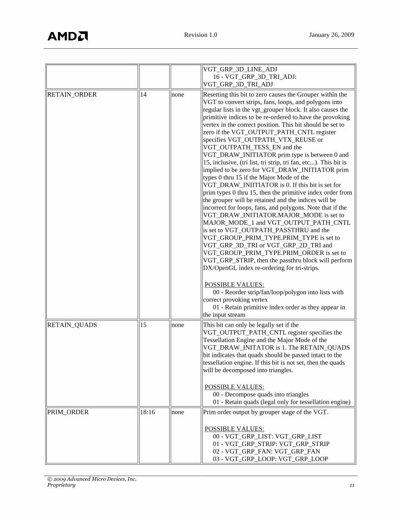
Revision 1.0 January 26, 2009
© 2009 Advanced Micro Devices, Inc. Proprietary 11
VGT_GRP_3D_LINE_ADJ
16 - VGT_GRP_3D_TRI_ADJ:
VGT_GRP_3D_TRI_ADJ
RETAIN_ORDER 14 none Resetting this bit to zero causes the Grouper within the
VGT to convert strips, fans, loops, and polygons into
regular lists in the vgt_grouper block. It also causes the
primitive indices to be re-ordered to have the provoking
vertex in the correct position. This bit should be set to
zero if the VGT_OUTPUT_PATH_CNTL register
specifies VGT_OUTPATH_VTX_REUSE or
VGT_OUTPATH_TESS_EN and the
VGT_DRAW_INITIATOR prim type is between 0 and
15, inclusive, (tri list, tri strip, tri fan, etc...). This bit is
implied to be zero for VGT_DRAW_INITIATOR prim
types 0 thru 15 if the Major Mode of the
VGT_DRAW_INIITIATOR is 0. If this bit is set for
prim types 0 thru 15, then the primitive index order from
the grouper will be retained and the indices will be
incorrect for loops, fans, and polygons. Note that if the
VGT_DRAW_INITIATOR.MAJOR_MODE is set to
MAJOR_MODE_1 and VGT_OUTPUT_PATH_CNTL
is set to VGT_OUTPATH_PASSTHRU and the
VGT_GROUP_PRIM_TYPE.PRIM_TYPE is set to
VGT_GRP_3D_TRI or VGT_GRP_2D_TRI and
VGT_GROUP_PRIM_TYPE.PRIM_ORDER is set to
VGT_GRP_STRIP, then the passthru block will perform
DX/OpenGL index re-ordering for tri-strips.
POSSIBLE VALUES:
00 - Reorder strip/fan/loop/polygon into lists with
correct provoking vertex
01 - Retain primitive index order as they appear in
the input stream
RETAIN_QUADS 15 none This bit can only be legally set if the
VGT_OUTPUT_PATH_CNTL register specifies the
Tessellation Engine and the Major Mode of the
VGT_DRAW_INITATOR is 1. The RETAIN_QUADS
bit indicates that quads should be passed intact to the
tessellation engine. If this bit is not set, then the quads
will be decomposed into triangles.
POSSIBLE VALUES:
00 - Decompose quads into triangles
01 - Retain quads (legal only for tessellation engine)
PRIM_ORDER 18:16 none Prim order output by grouper stage of the VGT.
POSSIBLE VALUES:
00 - VGT_GRP_LIST: VGT_GRP_LIST
01 - VGT_GRP_STRIP: VGT_GRP_STRIP
02 - VGT_GRP_FAN: VGT_GRP_FAN
03 - VGT_GRP_LOOP: VGT_GRP_LOOP

Revision 1.0 January 26, 2009
© 2009 Advanced Micro Devices, Inc. Proprietary 12
04 - VGT_GRP_POLYGON:
VGT_GRP_POLYGON
VGT:VGT_GROUP_VECT_0_CNTL · [R/W] · 32 bits · Access: 32 · GpuF0MMReg:0x28a30
DESCRIPTION: THIS REGISTER IS IGNORED IN MAJOR MODE 0 FOR PRIM TYPES 0 THRU 21 !! This
register indicates, with bits flags, which components are relevant for vector 0 of a group. At least one component of
vector 0 must be indicated. This register also contains the stride of vector 0 (in 16-bit words) in the input stream and
the amount to shift the input stream (in 16-bit words) after extracting the vector.
Field Name Bits Default Description
COMP_X_EN 0 none Indicates that component X will be output from the
grouper for vector 0
POSSIBLE VALUES:
00 - disable
01 - enable
COMP_Y_EN 1 none Indicates that component Y will be output from the
grouper for vector 0
POSSIBLE VALUES:
00 - disable
01 - enable
COMP_Z_EN 2 none Indicates that component Z will be output from the
grouper for vector 0
POSSIBLE VALUES:
00 - disable
01 - enable
COMP_W_EN 3 none Indicates that component W will be output from the
grouper for vector 0
POSSIBLE VALUES:
00 - disable
01 - enable
STRIDE 15:8 none The stride of vector 0 data in the input stream (in 16-bit
words). Zero is NOT a legal value for an active vector.
See the programming guidelines for the situation in
which a vector uses no data from the shifter.
SHIFT 23:16 none The amount to shift the input stream after extracting
vector 0 (in 16-bit words). This field must be less than or
equal to the STRIDE field for proper shifter operation.
VGT:VGT_GROUP_VECT_0_FMT_CNTL · [R/W] · 32 bits · Access: 32 · GpuF0MMReg:0x28a38
DESCRIPTION: THIS REGISTER IS IGNORED IN MAJOR MODE 0 FOR PRIM TYPES 0 THRU 21 !! This
register indicates how the value each component of vector 0 will be determined. If the
VGT_GROUP_VECT_0_CNTL register indicates that a particular component is not selected for output from the
grouper, then that component`s format control fields are ignored.

Revision 1.0 January 26, 2009
© 2009 Advanced Micro Devices, Inc. Proprietary 13
Field Name Bits Default Description
X_CONV 3:0 none X Component Determination.
POSSIBLE VALUES:
00 - VGT_GRP_INDEX_16:
VGT_GRP_INDEX_16 16 bits from stream with index
offset and clamp
01 - VGT_GRP_INDEX_32:
VGT_GRP_INDEX_32 32 bits from stream with index
offset and clamp
02 - VGT_GRP_UINT_16: VGT_GRP_UINT_16 16
bits from stream as unsigned int
03 - VGT_GRP_UINT_32: VGT_GRP_UINT_32 32
bits from stream as unsigned int
04 - VGT_GRP_SINT_16: VGT_GRP_SINT_16 16
bits from stream as signed int
05 - VGT_GRP_SINT_32: VGT_GRP_SINT_32 32
bits from stream as signed int
06 - VGT_GRP_FLOAT_32:
VGT_GRP_FLOAT_32 32 bits from stream as float
07 - VGT_GRP_AUTO_PRIM:
VGT_GRP_AUTO_PRIM 24 bits from auto primitive
counter
08 - VGT_GRP_FIX_1_23_TO_FLOAT:
VGT_GRP_FIX_1_23_TO_FLOAT 24 bit barycentric
value from tessellation engine
X_OFFSET 7:4 none X Component Offset. This field is the offset, in 16-bit
words, of the X component in the input cycle.
Y_CONV 11:8 none Y Component Determination. See the X component
determination field for description.
POSSIBLE VALUES:
00 - VGT_GRP_INDEX_16:
VGT_GRP_INDEX_16 16 bits from stream with index
offset and clamp
01 - VGT_GRP_INDEX_32:
VGT_GRP_INDEX_32 32 bits from stream with index
offset and clamp
02 - VGT_GRP_UINT_16: VGT_GRP_UINT_16 16
bits from stream as unsigned int
03 - VGT_GRP_UINT_32: VGT_GRP_UINT_32 32
bits from stream as unsigned int
04 - VGT_GRP_SINT_16: VGT_GRP_SINT_16 16
bits from stream as signed int
05 - VGT_GRP_SINT_32: VGT_GRP_SINT_32 32
bits from stream as signed int
06 - VGT_GRP_FLOAT_32:
VGT_GRP_FLOAT_32 32 bits from stream as float
07 - VGT_GRP_AUTO_PRIM:
VGT_GRP_AUTO_PRIM 24 bits from auto primitive
counter
08 - VGT_GRP_FIX_1_23_TO_FLOAT:

Revision 1.0 January 26, 2009
© 2009 Advanced Micro Devices, Inc. Proprietary 14
VGT_GRP_FIX_1_23_TO_FLOAT 24 bit barycentric
value from tessellation engine
Y_OFFSET 15:12 none Y Component Offset. This field is the offset, in 16-bit
words, of the Y component in the input cycle.
Z_CONV 19:16 none Z Component Determination. See the X component
determination field for description.
POSSIBLE VALUES:
00 - VGT_GRP_INDEX_16:
VGT_GRP_INDEX_16 16 bits from stream with index
offset and clamp
01 - VGT_GRP_INDEX_32:
VGT_GRP_INDEX_32 32 bits from stream with index
offset and clamp
02 - VGT_GRP_UINT_16: VGT_GRP_UINT_16 16
bits from stream as unsigned int
03 - VGT_GRP_UINT_32: VGT_GRP_UINT_32 32
bits from stream as unsigned int
04 - VGT_GRP_SINT_16: VGT_GRP_SINT_16 16
bits from stream as signed int
05 - VGT_GRP_SINT_32: VGT_GRP_SINT_32 32
bits from stream as signed int
06 - VGT_GRP_FLOAT_32:
VGT_GRP_FLOAT_32 32 bits from stream as float
07 - VGT_GRP_AUTO_PRIM:
VGT_GRP_AUTO_PRIM 24 bits from auto primitive
counter
08 - VGT_GRP_FIX_1_23_TO_FLOAT:
VGT_GRP_FIX_1_23_TO_FLOAT 24 bit barycentric
value from tessellation engine
Z_OFFSET 23:20 none Z Component Offset. This field is the offset, in 16-bit
words, of the Z component in the input cycle.
W_CONV 27:24 none W Component Determination. See the X component
determination field for description.
POSSIBLE VALUES:
00 - VGT_GRP_INDEX_16:
VGT_GRP_INDEX_16 16 bits from stream with index
offset and clamp
01 - VGT_GRP_INDEX_32:
VGT_GRP_INDEX_32 32 bits from stream with index
offset and clamp
02 - VGT_GRP_UINT_16: VGT_GRP_UINT_16 16
bits from stream as unsigned int
03 - VGT_GRP_UINT_32: VGT_GRP_UINT_32 32
bits from stream as unsigned int
04 - VGT_GRP_SINT_16: VGT_GRP_SINT_16 16
bits from stream as signed int
05 - VGT_GRP_SINT_32: VGT_GRP_SINT_32 32
bits from stream as signed int
06 - VGT_GRP_FLOAT_32:

Revision 1.0 January 26, 2009
© 2009 Advanced Micro Devices, Inc. Proprietary 15
VGT_GRP_FLOAT_32 32 bits from stream as float
07 - VGT_GRP_AUTO_PRIM:
VGT_GRP_AUTO_PRIM 24 bits from auto primitive
counter
08 - VGT_GRP_FIX_1_23_TO_FLOAT:
VGT_GRP_FIX_1_23_TO_FLOAT 24 bit barycentric
value from tessellation engine
W_OFFSET 31:28 none W Component Offset. This field is the offset, in 16-bit
words, of the Z component in the input cycle.
VGT:VGT_GROUP_VECT_1_CNTL · [R/W] · 32 bits · Access: 32 · GpuF0MMReg:0x28a34
DESCRIPTION: THIS REGISTER IS IGNORED IN MAJOR MODE 0 FOR PRIM TYPES 0 THRU 21 !! This
register is identical to VGT_GROUP_VECT_0_CNTL except that it applies to vector 1 of the group instead of
vector 0. Also, vector 0 is required to have at least one component set; however, vector 1 may have none set.
Field Name Bits Default Description
COMP_X_EN 0 none POSSIBLE VALUES:
00 - disable
01 - enable
COMP_Y_EN 1 none POSSIBLE VALUES:
00 - disable
01 - enable
COMP_Z_EN 2 none POSSIBLE VALUES:
00 - disable
01 - enable
COMP_W_EN 3 none POSSIBLE VALUES:
00 - disable
01 - enable
STRIDE 15:8 none
SHIFT 23:16 none
VGT:VGT_GROUP_VECT_1_FMT_CNTL · [R/W] · 32 bits · Access: 32 · GpuF0MMReg:0x28a3c
DESCRIPTION: THIS REGISTER IS IGNORED IN MAJOR MODE 0 FOR PRIM TYPES 0 THRU 21 !! This
register is identical to VGT_GROUP_VECT_0_FMT_CNTL except that it controls the formatting of output vector 1
instead of output vector 0.
Field Name Bits Default Description
X_CONV 3:0 none POSSIBLE VALUES:
00 - VGT_GRP_INDEX_16:
VGT_GRP_INDEX_16 16 bits from stream with index
offset and clamp
01 - VGT_GRP_INDEX_32:
VGT_GRP_INDEX_32 32 bits from stream with index
offset and clamp
02 - VGT_GRP_UINT_16: VGT_GRP_UINT_16 16
bits from stream as unsigned int
03 - VGT_GRP_UINT_32: VGT_GRP_UINT_32 32
bits from stream as unsigned int

Revision 1.0 January 26, 2009
© 2009 Advanced Micro Devices, Inc. Proprietary 16
04 - VGT_GRP_SINT_16: VGT_GRP_SINT_16 16
bits from stream as signed int
05 - VGT_GRP_SINT_32: VGT_GRP_SINT_32 32
bits from stream as signed int
06 - VGT_GRP_FLOAT_32:
VGT_GRP_FLOAT_32 32 bits from stream as float
07 - VGT_GRP_AUTO_PRIM:
VGT_GRP_AUTO_PRIM 24 bits from auto primitive
counter
08 - VGT_GRP_FIX_1_23_TO_FLOAT:
VGT_GRP_FIX_1_23_TO_FLOAT 24 bit barycentric
value from tessellation engine
X_OFFSET 7:4 none
Y_CONV 11:8 none POSSIBLE VALUES:
00 - VGT_GRP_INDEX_16:
VGT_GRP_INDEX_16 16 bits from stream with index
offset and clamp
01 - VGT_GRP_INDEX_32:
VGT_GRP_INDEX_32 32 bits from stream with index
offset and clamp
02 - VGT_GRP_UINT_16: VGT_GRP_UINT_16 16
bits from stream as unsigned int
03 - VGT_GRP_UINT_32: VGT_GRP_UINT_32 32
bits from stream as unsigned int
04 - VGT_GRP_SINT_16: VGT_GRP_SINT_16 16
bits from stream as signed int
05 - VGT_GRP_SINT_32: VGT_GRP_SINT_32 32
bits from stream as signed int
06 - VGT_GRP_FLOAT_32:
VGT_GRP_FLOAT_32 32 bits from stream as float
07 - VGT_GRP_AUTO_PRIM:
VGT_GRP_AUTO_PRIM 24 bits from auto primitive
counter
08 - VGT_GRP_FIX_1_23_TO_FLOAT:
VGT_GRP_FIX_1_23_TO_FLOAT 24 bit barycentric
value from tessellation engine
Y_OFFSET 15:12 none
Z_CONV 19:16 none POSSIBLE VALUES:
00 - VGT_GRP_INDEX_16:
VGT_GRP_INDEX_16 16 bits from stream with index
offset and clamp
01 - VGT_GRP_INDEX_32:
VGT_GRP_INDEX_32 32 bits from stream with index
offset and clamp
02 - VGT_GRP_UINT_16: VGT_GRP_UINT_16 16
bits from stream as unsigned int
03 - VGT_GRP_UINT_32: VGT_GRP_UINT_32 32
bits from stream as unsigned int
04 - VGT_GRP_SINT_16: VGT_GRP_SINT_16 16
bits from stream as signed int
05 - VGT_GRP_SINT_32: VGT_GRP_SINT_32 32
bits from stream as signed int

Revision 1.0 January 26, 2009
© 2009 Advanced Micro Devices, Inc. Proprietary 17
06 - VGT_GRP_FLOAT_32:
VGT_GRP_FLOAT_32 32 bits from stream as float
07 - VGT_GRP_AUTO_PRIM:
VGT_GRP_AUTO_PRIM 24 bits from auto primitive
counter
08 - VGT_GRP_FIX_1_23_TO_FLOAT:
VGT_GRP_FIX_1_23_TO_FLOAT 24 bit barycentric
value from tessellation engine
Z_OFFSET 23:20 none
W_CONV 27:24 none POSSIBLE VALUES:
00 - VGT_GRP_INDEX_16:
VGT_GRP_INDEX_16 16 bits from stream with index
offset and clamp
01 - VGT_GRP_INDEX_32:
VGT_GRP_INDEX_32 32 bits from stream with index
offset and clamp
02 - VGT_GRP_UINT_16: VGT_GRP_UINT_16 16
bits from stream as unsigned int
03 - VGT_GRP_UINT_32: VGT_GRP_UINT_32 32
bits from stream as unsigned int
04 - VGT_GRP_SINT_16: VGT_GRP_SINT_16 16
bits from stream as signed int
05 - VGT_GRP_SINT_32: VGT_GRP_SINT_32 32
bits from stream as signed int
06 - VGT_GRP_FLOAT_32:
VGT_GRP_FLOAT_32 32 bits from stream as float
07 - VGT_GRP_AUTO_PRIM:
VGT_GRP_AUTO_PRIM 24 bits from auto primitive
counter
08 - VGT_GRP_FIX_1_23_TO_FLOAT:
VGT_GRP_FIX_1_23_TO_FLOAT 24 bit barycentric
value from tessellation engine
W_OFFSET 31:28 none
VGT:VGT_GS_MODE · [R/W] · 32 bits · Access: 32 · GpuF0MMReg:0x28a40
DESCRIPTION: VGT GS Enable Mode
Field Name Bits Default Description
MODE 1:0 none Indicates which of GS scenerio is enabled
POSSIBLE VALUES:
00 - GS_OFF: GS_OFF
01 - GS_SCENARIO_A: GS_SCENARIO_A
02 - GS_SCENARIO_B: GS_SCENARIO_B
03 - GS_SCENARIO_G: GS_SCENARIO_G
ES_PASSTHRU 2 none sets to one if VS shader is passthru when GS scenario G
is used
POSSIBLE VALUES:
00 - passthru_dis
Revision 1.0 January 26, 2009
© 2009 Advanced Micro Devices, Inc. Proprietary 18
01 - passthru_en
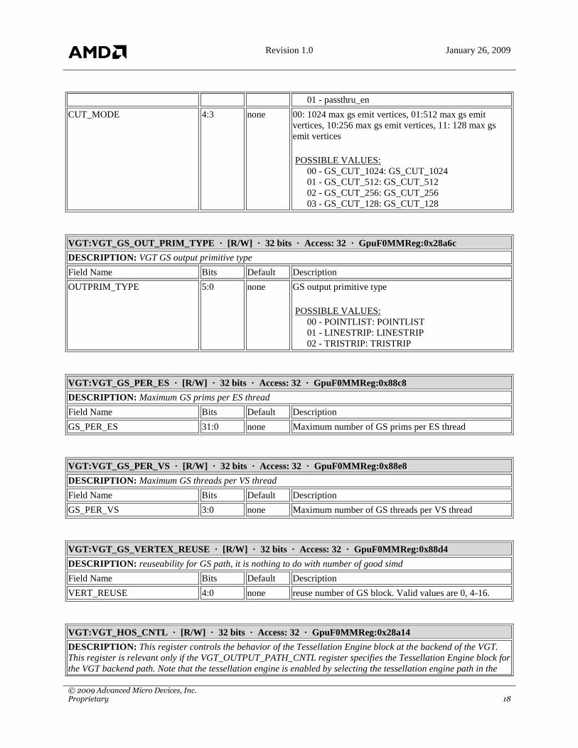
CUT_MODE 4:3 none 00: 1024 max gs emit vertices, 01:512 max gs emit
vertices, 10:256 max gs emit vertices, 11: 128 max gs
emit vertices
POSSIBLE VALUES:
00 - GS_CUT_1024: GS_CUT_1024
01 - GS_CUT_512: GS_CUT_512
02 - GS_CUT_256: GS_CUT_256
03 - GS_CUT_128: GS_CUT_128
VGT:VGT_GS_OUT_PRIM_TYPE · [R/W] · 32 bits · Access: 32 · GpuF0MMReg:0x28a6c
DESCRIPTION: VGT GS output primitive type
Field Name Bits Default Description
OUTPRIM_TYPE 5:0 none GS output primitive type
POSSIBLE VALUES:
00 - POINTLIST: POINTLIST
01 - LINESTRIP: LINESTRIP
02 - TRISTRIP: TRISTRIP
VGT:VGT_GS_PER_ES · [R/W] · 32 bits · Access: 32 · GpuF0MMReg:0x88c8
DESCRIPTION: Maximum GS prims per ES thread
Field Name Bits Default Description
GS_PER_ES 31:0 none Maximum number of GS prims per ES thread
VGT:VGT_GS_PER_VS · [R/W] · 32 bits · Access: 32 · GpuF0MMReg:0x88e8
DESCRIPTION: Maximum GS threads per VS thread
Field Name Bits Default Description
GS_PER_VS 3:0 none Maximum number of GS threads per VS thread
VGT:VGT_GS_VERTEX_REUSE · [R/W] · 32 bits · Access: 32 · GpuF0MMReg:0x88d4
DESCRIPTION: reuseability for GS path, it is nothing to do with number of good simd
Field Name Bits Default Description
VERT_REUSE 4:0 none reuse number of GS block. Valid values are 0, 4-16.
VGT:VGT_HOS_CNTL · [R/W] · 32 bits · Access: 32 · GpuF0MMReg:0x28a14
DESCRIPTION: This register controls the behavior of the Tessellation Engine block at the backend of the VGT.
This register is relevant only if the VGT_OUTPUT_PATH_CNTL register specifies the Tessellation Engine block for
the VGT backend path. Note that the tessellation engine is enabled by selecting the tessellation engine path in the

Revision 1.0 January 26, 2009
© 2009 Advanced Micro Devices, Inc. Proprietary 19
VGT_OUTPUT_PATH_CNTL register as opposed to the single enable bit that was used in previous architectures.
Field Name Bits Default Description
TESS_MODE 1:0 none Tessellation Mode
0 : Discrete
1 : Continuous
2 : Adaptive
VGT:VGT_HOS_MAX_TESS_LEVEL · [R/W] · 32 bits · Access: 32 · GpuF0MMReg:0x28a18
DESCRIPTION: For continuous and discrete tessellation modes, this register contains the tessellation level. For
adaptive tessellation, this register contains the maximum tessellation level. The adaptive tessellation levels will be
clamped less-than or equal to this level by the tessellation engine. In all cases, the format of this register is 32-bit
IEEE floating point. This register is relevant only when the VGT_OUT_CNTL register specifies `Tessellation
Engine` in the Path Select field.
Field Name Bits Default Description
MAX_TESS 31:0 none For adaptive tessellation mode, this is the maximum
tessellation clamp value.
For continuous and discrete tessellation modes, this is the
tessellation level.
For discrete modes, values in the range (1.0, 14.0) are
legal.
For non-discrete modes, values in the range (1.0, 15.0)
are legal.
MAX_TESS must be greater than or equal to
MIN_TESS.
VGT:VGT_HOS_MIN_TESS_LEVEL · [R/W] · 32 bits · Access: 32 · GpuF0MMReg:0x28a1c
DESCRIPTION: For continuous and discrete tessellation modes, this register is not applicable. For adaptive
tessellation, this register contains the minimum tessellation level. The adaptive tessellation levels will be clamped
greater-than or equal to this level by the tessellation engine. The format of this register is 32-bit IEEE floating
point. This register is relevant only when the VGT_OUT_CNTL register specifies `Tessellation Engine` in the Path
Select field and the VGT_HOS_CNTL register specifies adaptive tessellation mode.
Field Name Bits Default Description
MIN_TESS 31:0 none For adpative tessellation mode, this is the minimum
tessellation clamp value.
For continuous and discrete tessellartion modes, this
register is not applicable.
For discrete modes values in the range (1.0, 14.0) are
legal.
For non-discrete modes, values in the range (1.0, 15.0)
are legal.
MIN_TESS must be less than or equal to MAX_TESS.
VGT:VGT_HOS_REUSE_DEPTH · [R/W] · 32 bits · Access: 32 · GpuF0MMReg:0x28a20
Field Name Bits Default Description
REUSE_DEPTH 7:0 none

Revision 1.0 January 26, 2009
© 2009 Advanced Micro Devices, Inc. Proprietary 20
VGT:VGT_IMMED_DATA · [W] · 32 bits · Access: 32 · GpuF0MMReg:0x287f4
DESCRIPTION: VGT Immediate Data
Field Name Bits Default Description
DATA 31:0 none Data written to this address is written into the VGT
Immediate Data FIFO.
VGT:VGT_INDEX_TYPE · [W] · 32 bits · Access: 32 · GpuF0MMReg:0x895c
DESCRIPTION: VGT Index Type
Field Name Bits Default Description
INDEX_TYPE 1:0 none Index Type (applicable to prim types 0-28 only).
If the Source Select field is set to `Auto-increment Index`
mode, then this field is ignored and the index type is 32-
bits per index
POSSIBLE VALUES:
00 - DI_INDEX_SIZE_16_BIT:
DI_INDEX_SIZE_16_BIT 16 bits per index
01 - DI_INDEX_SIZE_32_BIT:
DI_INDEX_SIZE_32_BIT 32 bits per index
VGT:VGT_INDX_OFFSET · [R/W] · 32 bits · Access: 32 · GpuF0MMReg:0x28408
DESCRIPTION: For components that are that are specified to be indices (see the
VGT_GROUP_VECT_0_FMT_CNTL register), this register is the offset value. Offsetting occurs prior to clamping
and fix->flt conversion.
Field Name Bits Default Description
INDX_OFFSET 31:0 none Index offset value (32-bit adder), extend it to 32-bits
VGT:VGT_INSTANCE_STEP_RATE_0 · [R/W] · 32 bits · Access: 32 · GpuF0MMReg:0x28aa0
DESCRIPTION: This register defines the first instance step rate
Field Name Bits Default Description
STEP_RATE 31:0 none Instance step rate
VGT:VGT_INSTANCE_STEP_RATE_1 · [R/W] · 32 bits · Access: 32 · GpuF0MMReg:0x28aa4
DESCRIPTION: This register defines the second instance step rate
Field Name Bits Default Description
STEP_RATE 31:0 none Instance step rate
VGT:VGT_LAST_COPY_STATE · [R] · 32 bits · Access: 32 · GpuF0MMReg:0x88c0

Revision 1.0 January 26, 2009
© 2009 Advanced Micro Devices, Inc. Proprietary 21
DESCRIPTION: This register retains the data from the last GFX_COPY_STATE command.
Field Name Bits Default Description
SRC_STATE_ID 2:0 none Source context from last GFX_COPY_STATE
command.
DST_STATE_ID 18:16 none Destination context from last GFX_COPY_STATE
command.
VGT:VGT_MAX_VTX_INDX · [R/W] · 32 bits · Access: 32 · GpuF0MMReg:0x28400
DESCRIPTION: For components that are that are specified to be indices (see the
VGT_GROUP_VECT_0_FMT_CNTL register), this register is the maximum clamp value. Clamping occurs after
offsetting and prior to fix->flt conversion.
Field Name Bits Default Description
MAX_INDX 31:0 none maximum clamp value for index clamp, exten it to 32-bit
VGT:VGT_MC_LAT_CNTL · [R/W] · 32 bits · Access: 32 · GpuF0MMReg:0x88d8
DESCRIPTION: Time Stamp Counter Resolution Select
Field Name Bits Default Description
MC_TIME_STAMP_RES 1:0 0x0 Select the counter resolution for tracking memory
controller latency
POSSIBLE VALUES:
00 - 0 -> 992 max latency, step of 32
01 - 0 -> 496 max latency, step of 16
02 - 0 -> 248 max latency, step of 8
03 - 0 -> 124 max latency, step of 4
VGT:VGT_MIN_VTX_INDX · [R/W] · 32 bits · Access: 32 · GpuF0MMReg:0x28404
DESCRIPTION: For components that are that are specified to be indices (see the
VGT_GROUP_VECT_0_FMT_CNTL register), this register is the minimum clamp value. Clamping occurs after
offsetting and prior to fix->flt conversion.
Field Name Bits Default Description
MIN_INDX 31:0 none minimum clamp value for index clamp, extend it to 32-
bits
VGT:VGT_MULTI_PRIM_IB_RESET_EN · [R/W] · 32 bits · Access: 32 · GpuF0MMReg:0x28a94
DESCRIPTION: This register enabling reseting of prim based on reset index
Field Name Bits Default Description
RESET_EN 0 none IF SET, THEN RESET INDEX IS USED FOR
RESETING A PRIM
POSSIBLE VALUES:

Revision 1.0 January 26, 2009
© 2009 Advanced Micro Devices, Inc. Proprietary 22
00 - multi_prim reset off
01 - multi_prim reset on
VGT:VGT_MULTI_PRIM_IB_RESET_INDX · [R/W] · 32 bits · Access: 32 · GpuF0MMReg:0x2840c
DESCRIPTION: This register defines the index which resets primitive sets when MULTI_PRIM_IB is enabled.
Field Name Bits Default Description
RESET_INDX 31:0 none If this value matches an index in the IB, a new primitive
set is started.
VGT:VGT_NUM_INDICES · [W] · 32 bits · Access: 32 · GpuF0MMReg:0x8970
DESCRIPTION: VGT Number of Indices
Field Name Bits Default Description
NUM_INDICES 31:0 none This field indicates the number of indices to process for
this draw initiator. Note this count is not necessarily the
count of the primitives. It is also not the index buffer size
in memory.
VGT:VGT_NUM_INSTANCES · [W] · 32 bits · Access: 32 · GpuF0MMReg:0x8974
DESCRIPTION: VGT Number of Instances
Field Name Bits Default Description
NUM_INSTANCES 31:0 none VGT Number of Instances
VGT:VGT_OUTPUT_PATH_CNTL · [R/W] · 32 bits · Access: 32 · GpuF0MMReg:0x28a10
DESCRIPTION: THIS REGISTER IS IGNORED IN MAJOR MODE 0 FOR PRIM TYPES 0 THRU 21 !! This
register selects which backend path will be used by the VGT block.
Field Name Bits Default Description
PATH_SELECT 1:0 none This field indicates the VGT back-end path to be used.
POSSIBLE VALUES:
00 - VGT_OUTPATH_VTX_REUSE:
VGT_OUTPATH_VTX_REUSE
01 - VGT_OUTPATH_TESS_EN:
VGT_OUTPATH_TESS_EN
02 - VGT_OUTPATH_PASSTHRU:
VGT_OUTPATH_PASSTHRU
03 - VGT_OUTPATH_GS_BLOCK:
VGT_OUTPATH_GS_BLOCK
VGT:VGT_OUT_DEALLOC_CNTL · [R/W] · 32 bits · Access: 32 · GpuF0MMReg:0x28c5c
DESCRIPTION: This register controls, within a process vector, when the previous process vector is de-allocated.
Revision 1.0 January 26, 2009
© 2009 Advanced Micro Devices, Inc. Proprietary 23
Field Name Bits Default Description
DEALLOC_DIST 6:0 none Distance (in indices) which the vertex vector slot
assignment leads the deallocation. This field should
typically be set to (num_enabled_pipes * 4).
VGT:VGT_PRIMITIVEID_EN · [R/W] · 32 bits · Access: 32 · GpuF0MMReg:0x28a84
DESCRIPTION: VGT Primitive ID enable
Field Name Bits Default Description
PRIMITIVEID_EN 0 none PrimitiveID generation is enabled
POSSIBLE VALUES:
00 - suppress PrimitiveID output
01 - output primitiveID
VGT:VGT_PRIMITIVE_TYPE · [W] · 32 bits · Access: 32 · GpuF0MMReg:0x8958
DESCRIPTION: VGT Primitive Type
Field Name Bits Default Description
PRIM_TYPE 5:0 none Primitive Type
POSSIBLE VALUES:
00 - DI_PT_NONE: DI_PT_NONE None (does not
create draw trigger)
01 - DI_PT_POINTLIST: DI_PT_POINTLIST Point
List
02 - DI_PT_LINELIST: DI_PT_LINELIST Line List
03 - DI_PT_LINESTRIP: DI_PT_LINESTRIP Line
Strip
04 - DI_PT_TRILIST: DI_PT_TRILIST Tri List
05 - DI_PT_TRIFAN: DI_PT_TRIFAN Tri Fan
06 - DI_PT_TRISTRIP: DI_PT_TRISTRIP Tri Strip
07 - DI_PT_UNUSED_0: DI_PT_UNUSED_0
Reserved 1
08 - DI_PT_UNUSED_1: DI_PT_UNUSED_1
Reserved 2
09 - DI_PT_UNUSED_2: DI_PT_UNUSED_2
Reserved 3
10 - DI_PT_LINELIST_ADJ:
DI_PT_LINELIST_ADJ Adjacent Line List
11 - DI_PT_LINESTRIP_ADJ:
DI_PT_LINESTRIP_ADJ Adjacent Line Strip
12 - DI_PT_TRILIST_ADJ: DI_PT_TRILIST_ADJ
Adjacent Tri List
13 - DI_PT_TRISTRIP_ADJ:
DI_PT_TRISTRIP_ADJ Adjacent Tri Strip
14 - DI_PT_UNUSED_3: DI_PT_UNUSED_3
Reserved 3
15 - DI_PT_UNUSED_4: DI_PT_UNUSED_4

Revision 1.0 January 26, 2009
© 2009 Advanced Micro Devices, Inc. Proprietary 24
Reserved 4
16 - DI_PT_TRI_WITH_WFLAGS:
DI_PT_TRI_WITH_WFLAGS Tri List w/Flags (legacy
R128)
17 - DI_PT_RECTLIST: DI_PT_RECTLIST Rect
List
18 - DI_PT_LINELOOP: DI_PT_LINELOOP Line
LOOP
19 - DI_PT_QUADLIST: DI_PT_QUADLIST Quad
List
20 - DI_PT_QUADSTRIP: DI_PT_QUADSTRIP
Quad Strip
21 - DI_PT_POLYGON: DI_PT_POLYGON
Polygon
22 - DI_PT_2D_COPY_RECT_LIST_V0:
DI_PT_2D_COPY_RECT_LIST_V0 2D Copy Rect List
V0
23 - DI_PT_2D_COPY_RECT_LIST_V1:
DI_PT_2D_COPY_RECT_LIST_V1 2D Copy Rect List
V1
24 - DI_PT_2D_COPY_RECT_LIST_V2:
DI_PT_2D_COPY_RECT_LIST_V2 2D Copy Rect List
V2
25 - DI_PT_2D_COPY_RECT_LIST_V3:
DI_PT_2D_COPY_RECT_LIST_V3 2D Copy Rect List
V3
26 - DI_PT_2D_FILL_RECT_LIST:
DI_PT_2D_FILL_RECT_LIST 2D Fill Rect List
27 - DI_PT_2D_LINE_STRIP:
DI_PT_2D_LINE_STRIP 2D Line Strip
28 - DI_PT_2D_TRI_STRIP:
DI_PT_2D_TRI_STRIP 2D Triangle Strip
VGT:VGT_REUSE_OFF · [R/W] · 32 bits · Access: 32 · GpuF0MMReg:0x28ab4
DESCRIPTION: VGT reuse is off. This will expand strip primitives to list primitives
Field Name Bits Default Description
REUSE_OFF 0 none reuse is off (set to 1)
POSSIBLE VALUES:
00 - Reuse on
01 - Reuse off
VGT:VGT_STRMOUT_BASE_OFFSET_0 · [R/W] · 32 bits · Access: 32 · GpuF0MMReg:0x28b10
DESCRIPTION: Stream out base_0 + offset_0. This register is snooped by SQ.
Field Name Bits Default Description
BASE_OFFSET 31:0 none DWORD base+offset for given stream out buffer. Set by
CP or driver.
Revision 1.0 January 26, 2009
© 2009 Advanced Micro Devices, Inc. Proprietary 25
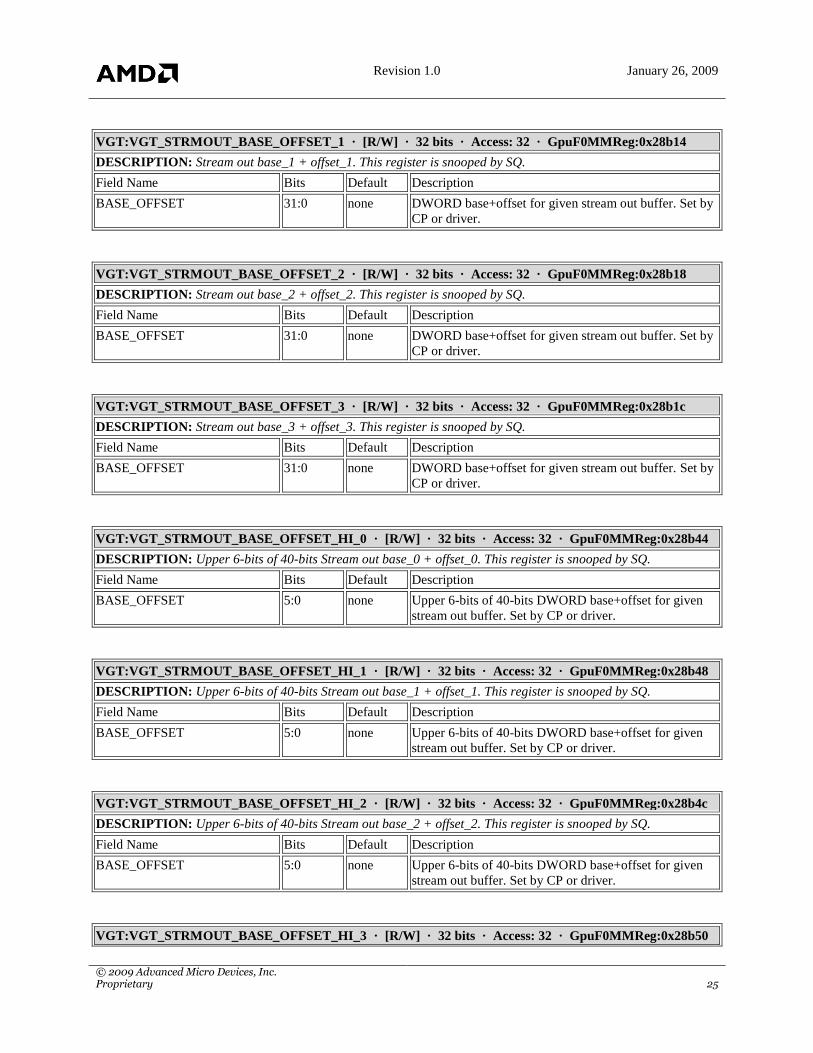
VGT:VGT_STRMOUT_BASE_OFFSET_1 · [R/W] · 32 bits · Access: 32 · GpuF0MMReg:0x28b14
DESCRIPTION: Stream out base_1 + offset_1. This register is snooped by SQ.
Field Name Bits Default Description
BASE_OFFSET 31:0 none DWORD base+offset for given stream out buffer. Set by
CP or driver.
VGT:VGT_STRMOUT_BASE_OFFSET_2 · [R/W] · 32 bits · Access: 32 · GpuF0MMReg:0x28b18
DESCRIPTION: Stream out base_2 + offset_2. This register is snooped by SQ.
Field Name Bits Default Description
BASE_OFFSET 31:0 none DWORD base+offset for given stream out buffer. Set by
CP or driver.
VGT:VGT_STRMOUT_BASE_OFFSET_3 · [R/W] · 32 bits · Access: 32 · GpuF0MMReg:0x28b1c
DESCRIPTION: Stream out base_3 + offset_3. This register is snooped by SQ.
Field Name Bits Default Description
BASE_OFFSET 31:0 none DWORD base+offset for given stream out buffer. Set by
CP or driver.
VGT:VGT_STRMOUT_BASE_OFFSET_HI_0 · [R/W] · 32 bits · Access: 32 · GpuF0MMReg:0x28b44
DESCRIPTION: Upper 6-bits of 40-bits Stream out base_0 + offset_0. This register is snooped by SQ.
Field Name Bits Default Description
BASE_OFFSET 5:0 none Upper 6-bits of 40-bits DWORD base+offset for given
stream out buffer. Set by CP or driver.
VGT:VGT_STRMOUT_BASE_OFFSET_HI_1 · [R/W] · 32 bits · Access: 32 · GpuF0MMReg:0x28b48
DESCRIPTION: Upper 6-bits of 40-bits Stream out base_1 + offset_1. This register is snooped by SQ.
Field Name Bits Default Description
BASE_OFFSET 5:0 none Upper 6-bits of 40-bits DWORD base+offset for given
stream out buffer. Set by CP or driver.
VGT:VGT_STRMOUT_BASE_OFFSET_HI_2 · [R/W] · 32 bits · Access: 32 · GpuF0MMReg:0x28b4c
DESCRIPTION: Upper 6-bits of 40-bits Stream out base_2 + offset_2. This register is snooped by SQ.
Field Name Bits Default Description
BASE_OFFSET 5:0 none Upper 6-bits of 40-bits DWORD base+offset for given
stream out buffer. Set by CP or driver.
VGT:VGT_STRMOUT_BASE_OFFSET_HI_3 · [R/W] · 32 bits · Access: 32 · GpuF0MMReg:0x28b50

Revision 1.0 January 26, 2009
© 2009 Advanced Micro Devices, Inc. Proprietary 26
DESCRIPTION: Upper 6-bits of 40-bits Stream out base_3 + offset_3. This register is snooped by SQ.
Field Name Bits Default Description
BASE_OFFSET 5:0 none Upper 6-bits of 40-bits DWORD base+offset for given
stream out buffer. Set by CP or driver.
VGT:VGT_STRMOUT_BUFFER_BASE_0 · [R/W] · 32 bits · Access: 32 · GpuF0MMReg:0x28ad8
DESCRIPTION: Stream-out base.
Field Name Bits Default Description
BASE 31:0 none DWORD Buffer base for given stream out buffer. Bits
31:0 corresponds to 39:8 of memory address. This data
can be stored in the coherency registers. This register is
snooped by CP.
VGT:VGT_STRMOUT_BUFFER_BASE_1 · [R/W] · 32 bits · Access: 32 · GpuF0MMReg:0x28ae8
DESCRIPTION: Stream-out base.
Field Name Bits Default Description
BASE 31:0 none DWORD Buffer base for given stream out buffer. Bits
31:0 corresponds to 39:8 of memory address. This data
can be stored in the coherency registers. This register is
snooped by CP.
VGT:VGT_STRMOUT_BUFFER_BASE_2 · [R/W] · 32 bits · Access: 32 · GpuF0MMReg:0x28af8
DESCRIPTION: Stream-out base.
Field Name Bits Default Description
BASE 31:0 none DWORD Buffer base for given stream out buffer. Bits
31:0 corresponds to 39:8 of memory address. This data
can be stored in the coherency registers. This register is
snooped by CP.
VGT:VGT_STRMOUT_BUFFER_BASE_3 · [R/W] · 32 bits · Access: 32 · GpuF0MMReg:0x28b08
DESCRIPTION: Stream-out base.
Field Name Bits Default Description
BASE 31:0 none DWORD Buffer base for given stream out buffer. Bits
31:0 corresponds to 39:8 of memory address. This data
can be stored in the coherency registers. This register is
snooped by CP.
VGT:VGT_STRMOUT_BUFFER_EN · [R/W] · 32 bits · Access: 32 · GpuF0MMReg:0x28b20
DESCRIPTION: Stream out enable bits. CP will use for SO coherency register validness.
Field Name Bits Default Description

Revision 1.0 January 26, 2009
© 2009 Advanced Micro Devices, Inc. Proprietary 27
BUFFER_0_EN 0 none Enable buffer 0 stream out.
BUFFER_1_EN 1 none Enable buffer 1 stream out.
BUFFER_2_EN 2 none Enable buffer 2 stream out.
BUFFER_3_EN 3 none Enable buffer 3 stream out.
VGT:VGT_STRMOUT_BUFFER_FILLED_SIZE_0 · [R/W] · 32 bits · Access: 32 ·
GpuF0MMReg:0x8960
DESCRIPTION: Stream-out adjusted size.
Field Name Bits Default Description
SIZE 31:0 none DWORD Sum of (SO_BufferOffset +
BufDwordWritten) for given buffer. Read Only. To read
this register the VGT needs to be flushed to the point
BufDwordWritten counts are maintained.
VGT:VGT_STRMOUT_BUFFER_FILLED_SIZE_1 · [R/W] · 32 bits · Access: 32 ·
GpuF0MMReg:0x8964
DESCRIPTION: Stream-out adjusted size.
Field Name Bits Default Description
SIZE 31:0 none DWORD Sum of (SO_BufferOffset +
BufDwordWritten) for given buffer. Read Only. To read
this register the VGT needs to be flushed to the point
BufDwordWritten counts are maintained.
VGT:VGT_STRMOUT_BUFFER_FILLED_SIZE_2 · [R/W] · 32 bits · Access: 32 ·
GpuF0MMReg:0x8968
DESCRIPTION: Stream-out adjusted size.
Field Name Bits Default Description
SIZE 31:0 none DWORD Sum of (SO_BufferOffset +
BufDwordWritten) for given buffer. Read Only. To read
this register the VGT needs to be flushed to the point
BufDwordWritten counts are maintained.
VGT:VGT_STRMOUT_BUFFER_FILLED_SIZE_3 · [R/W] · 32 bits · Access: 32 ·
GpuF0MMReg:0x896c
DESCRIPTION: Stream-out adjusted size.
Field Name Bits Default Description
SIZE 31:0 none DWORD Sum of (SO_BufferOffset +
BufDwordWritten) for given buffer. Read Only. To read
this register the VGT needs to be flushed to the point
BufDwordWritten counts are maintained.

Revision 1.0 January 26, 2009
© 2009 Advanced Micro Devices, Inc. Proprietary 28
VGT:VGT_STRMOUT_BUFFER_OFFSET_0 · [R/W] · 32 bits · Access: 32 · GpuF0MMReg:0x28adc
DESCRIPTION: Stream out offset.
Field Name Bits Default Description
OFFSET 31:0 none DWORD offset for given stream out buffer. Writing this
register will cause the VGT to load a Zero into
BufDwordWritten[4] and SO_CurVertIndex.
VGT:VGT_STRMOUT_BUFFER_OFFSET_1 · [R/W] · 32 bits · Access: 32 · GpuF0MMReg:0x28aec
DESCRIPTION: Stream out offset.
Field Name Bits Default Description
OFFSET 31:0 none DWORD offset for given stream out buffer. Writing this
register will cause the VGT to load a Zero into
BufDwordWritten[4] and SO_CurVertIndex.
VGT:VGT_STRMOUT_BUFFER_OFFSET_2 · [R/W] · 32 bits · Access: 32 · GpuF0MMReg:0x28afc
DESCRIPTION: Stream out offset.
Field Name Bits Default Description
OFFSET 31:0 none DWORD offset for given stream out buffer. Writing this
register will cause the VGT to load a Zero into
BufDwordWritten[4] and SO_CurVertIndex.
VGT:VGT_STRMOUT_BUFFER_OFFSET_3 · [R/W] · 32 bits · Access: 32 · GpuF0MMReg:0x28b0c
DESCRIPTION: Stream out offset.
Field Name Bits Default Description
OFFSET 31:0 none DWORD offset for given stream out buffer. Writing this
register will cause the VGT to load a Zero into
BufDwordWritten[4] and SO_CurVertIndex.
VGT:VGT_STRMOUT_BUFFER_SIZE_0 · [R/W] · 32 bits · Access: 32 · GpuF0MMReg:0x28ad0
DESCRIPTION: Stream-out size.
Field Name Bits Default Description
SIZE 31:0 none DWORD Buffer size for given stream out buffer.
VGT:VGT_STRMOUT_BUFFER_SIZE_1 · [R/W] · 32 bits · Access: 32 · GpuF0MMReg:0x28ae0
DESCRIPTION: Stream-out size.
Field Name Bits Default Description
SIZE 31:0 none DWORD Buffer size for given stream out buffer.

Revision 1.0 January 26, 2009
© 2009 Advanced Micro Devices, Inc. Proprietary 29
VGT:VGT_STRMOUT_BUFFER_SIZE_2 · [R/W] · 32 bits · Access: 32 · GpuF0MMReg:0x28af0
DESCRIPTION: Stream-out size.
Field Name Bits Default Description
SIZE 31:0 none DWORD Buffer size for given stream out buffer.
VGT:VGT_STRMOUT_BUFFER_SIZE_3 · [R/W] · 32 bits · Access: 32 · GpuF0MMReg:0x28b00
DESCRIPTION: Stream-out size.
Field Name Bits Default Description
SIZE 31:0 none DWORD Buffer size for given stream out buffer.
VGT:VGT_STRMOUT_DRAW_OPAQUE_BUFFER_FILLED_SIZE · [R/W] · 32 bits · Access: 32 ·
GpuF0MMReg:0x28b2c
DESCRIPTION: Draw opaque size.
Field Name Bits Default Description
SIZE 31:0 none This will be loaded by the CP for a DrawOpaque call by
fetching a memory address containing last
bufferfilledsize associated with the previous stream out
buffer bound to the IA.
VGT:VGT_STRMOUT_DRAW_OPAQUE_OFFSET · [R/W] · 32 bits · Access: 32 ·
GpuF0MMReg:0x28b28
DESCRIPTION: Draw opaque offset.
Field Name Bits Default Description
OFFSET 31:0 none pOffsets from the IASetVertexBuffers binding of a
stream out buffer that is to be used as src data. The
retrived BufferFilledSize minus this poffset if positive,
will determine the amount of data from which primitives
can be created.
VGT:VGT_STRMOUT_DRAW_OPAQUE_VERTEX_STRIDE · [R/W] · 32 bits · Access: 32 ·
GpuF0MMReg:0x28b30
DESCRIPTION: Draw opaque vertex stride.
Field Name Bits Default Description
VERTEX_STRIDE 31:0 none vertex stride used for draw opaque call
VGT:VGT_STRMOUT_EN · [R/W] · 32 bits · Access: 32 · GpuF0MMReg:0x28ab0
DESCRIPTION: This register enables streaming out
Field Name Bits Default Description
STREAMOUT 0 none If set, streaming output is enabled

Revision 1.0 January 26, 2009
© 2009 Advanced Micro Devices, Inc. Proprietary 30
POSSIBLE VALUES:
00 - STREAMOUT OFF
01 - STREAMOUT ON
VGT:VGT_STRMOUT_VTX_STRIDE_0 · [R/W] · 32 bits · Access: 32 · GpuF0MMReg:0x28ad4
DESCRIPTION: Stream out stride.
Field Name Bits Default Description
STRIDE 9:0 none DWORD stride between vertices in given stream-out
buffer. From stream output declarations details of dx10
spec, the max stride 2048 bytes or 512 words defined to
be the spacing between the beginning of each vertex.
VGT:VGT_STRMOUT_VTX_STRIDE_1 · [R/W] · 32 bits · Access: 32 · GpuF0MMReg:0x28ae4
DESCRIPTION: Stream out stride.
Field Name Bits Default Description
STRIDE 9:0 none DWORD stride between vertices in given stream-out
buffer. From stream output declarations details of dx10
spec, the max stride 2048 bytes or 512 words defined to
be the spacing between the beginning of each vertex.
VGT:VGT_STRMOUT_VTX_STRIDE_2 · [R/W] · 32 bits · Access: 32 · GpuF0MMReg:0x28af4
DESCRIPTION: Stream out stride.
Field Name Bits Default Description
STRIDE 9:0 none DWORD stride between vertices in given stream-out
buffer. From stream output declarations details of dx10
spec, the max stride 2048 bytes or 512 words defined to
be the spacing between the beginning of each vertex.
VGT:VGT_STRMOUT_VTX_STRIDE_3 · [R/W] · 32 bits · Access: 32 · GpuF0MMReg:0x28b04
DESCRIPTION: Stream out stride.
Field Name Bits Default Description
STRIDE 9:0 none DWORD stride between vertices in given stream-out
buffer. From stream output declarations details of dx10
spec, the max stride 2048 bytes or 512 words defined to
be the spacing between the beginning of each vertex.
VGT:VGT_VERTEX_REUSE_BLOCK_CNTL · [R/W] · 32 bits · Access: 32 · GpuF0MMReg:0x28c58
DESCRIPTION: This register controls the behavior of the Vertex Reuse block at the backend of the VGT. This
register is relevant only if the VGT_OUTPUT_PATH_CNTL register (or the prim type in Major Mode 0) specifies

Revision 1.0 January 26, 2009
© 2009 Advanced Micro Devices, Inc. Proprietary 31
the Vertex Reuse Block for the VGT backend path.
Field Name Bits Default Description
VTX_REUSE_DEPTH 7:0 none In general, for processing triangles, the vertex reuse
depth should be programmed to ((num_enabled_pipes *
4) - 2)
VGT:VGT_VTX_CNT_EN · [R/W] · 32 bits · Access: 32 · GpuF0MMReg:0x28ab8
DESCRIPTION: Auto -index generation is on.
Field Name Bits Default Description
VTX_CNT_EN 0 none Set to one if auto index generation is enabled
POSSIBLE VALUES:
00 - Auto off
01 - Auto on
VGT:VGT_VTX_VECT_EJECT_REG · [R/W] · 32 bits · Access: 32 · GpuF0MMReg:0x88b0
DESCRIPTION: This register defines the number of primitives that are allowed to pass during the assembly of a
single vertex vector. After this number of primitives have passed, the vertex vector is submitted to the shaders for
processing even if it is not full.
Field Name Bits Default Description
PRIM_COUNT 9:0 0x7F This is the count of primitives allowed to pass during the
assembly of a single vertex vector.

Revision 1.0 January 26, 2009
© 2009 Advanced Micro Devices, Inc. Proprietary 32
2. Primitive Assembly Registers
PA:PA_CL_CLIP_CNTL · [R/W] · 32 bits · Access: 32 · GpuF0MMReg:0x28810
DESCRIPTION: Clipper Control Bits
Field Name Bits Default Description
UCP_ENA_0 0 none Enable User-Clip Plane 0
UCP_ENA_1 1 none Enable User-Clip Plane 1
UCP_ENA_2 2 none Enable User-Clip Plane 2
UCP_ENA_3 3 none Enable User-Clip Plane 3
UCP_ENA_4 4 none Enable User-Clip Plane 4
UCP_ENA_5 5 none Enable User-Clip Plane 5
PS_UCP_Y_SCALE_NEG 13 none
PS_UCP_MODE 15:14 none 0 = Cull using distance from center of point
1 = Cull using radius-based distance from center of
point
2 = Cull using radius-based distance from center of
point, Expand and Clip on intersection
3 = Always expand and clip as trifan
CLIP_DISABLE 16 none Disables clip code generation and clipping process for
TCL
UCP_CULL_ONLY_ENA 17 none Cull Primitives against UCPS, but don`t clip
BOUNDARY_EDGE_FLAG_ENA 18 none Currently unused: Pending Delete. Left as placeholder
for now.
DX_CLIP_SPACE_DEF 19 none Clip space is defined as:
0: -W < X < W, -W < Y < W, -W < Z < W (OpenGL
Definition)
1: -W < X < W, -W < Y < W, 0 < Z < W (DirectX
Definition)
DIS_CLIP_ERR_DETECT 20 none Disables culling of primitives for which the clipped
detects an error. Default is 0
VTX_KILL_OR 21 none Used if Vertex Kill flags are exported from Vertex
Shader. If clear, ALL vertices for current primitive
must be set to kill the primitive (�AND� MODE). If
set, if ANY vertices for current primitive are set, the
the primitive will be killed (�OR� MODE).
DX_LINEAR_ATTR_CLIP_ENA 24 none
VTE_VPORT_PROVOKE_DISABLE 25 none
ZCLIP_NEAR_DISABLE 26 none
ZCLIP_FAR_DISABLE 27 none
PA:PA_CL_CNTL_STATUS · [R] · 32 bits · Access: 32 · GpuF0MMReg:0x8a10
DESCRIPTION: Status Bits
Field Name Bits Default Description

Revision 1.0 January 26, 2009
© 2009 Advanced Micro Devices, Inc. Proprietary 33
CL_BUSY 31 none Busy Status Bit
PA:PA_CL_ENHANCE · [R/W] · 32 bits · Access: 32 · GpuF0MMReg:0x8a14
DESCRIPTION: Used for Late Additions of Control Bits
Field Name Bits Default Description
CLIP_VTX_REORDER_ENA 0 none Enables vertex-order-independent clipping
NUM_CLIP_SEQ 2:1 none Number of Clip Sequences Active (+1). Should be set to
3 (4 sequences) for best performance
CLIPPED_PRIM_SEQ_STALL 3 none Forces a faster clip path if NUM_CLIP_SEQ is set to 0
(which should only be if 3 does not work)
VE_NAN_PROC_DISABLE 4 none
PA:PA_CL_GB_HORZ_CLIP_ADJ · [R/W] · 32 bits · Access: 32 · GpuF0MMReg:0x28c14
DESCRIPTION: Horizontal Guard Band Clip Adjust Register
Field Name Bits Default Description
DATA_REGISTER 31:0 none 32-bit floating point value. Should be set to 1.0 for no
guard band.
PA:PA_CL_GB_HORZ_DISC_ADJ · [R/W] · 32 bits · Access: 32 · GpuF0MMReg:0x28c18
DESCRIPTION: Horizontal Guard Band Discard Adjust Register
Field Name Bits Default Description
DATA_REGISTER 31:0 none 32-bit floating point value. Should be set to 1.0 for no
guard band.
PA:PA_CL_GB_VERT_CLIP_ADJ · [R/W] · 32 bits · Access: 32 · GpuF0MMReg:0x28c0c
DESCRIPTION: Vertical Guard Band Clip Adjust Register
Field Name Bits Default Description
DATA_REGISTER 31:0 none 32-bit floating point value. Should be set to 1.0 for no
guard band.
PA:PA_CL_GB_VERT_DISC_ADJ · [R/W] · 32 bits · Access: 32 · GpuF0MMReg:0x28c10
DESCRIPTION: Vertical Guard Band Discard Adjust Register
Field Name Bits Default Description
DATA_REGISTER 31:0 none 32-bit floating point value. Should be set to 1.0 for no
guard band.
PA:PA_CL_NANINF_CNTL · [R/W] · 32 bits · Access: 32 · GpuF0MMReg:0x28820

Revision 1.0 January 26, 2009
© 2009 Advanced Micro Devices, Inc. Proprietary 34
Field Name Bits Default Description
VTE_XY_INF_DISCARD 0 none
VTE_Z_INF_DISCARD 1 none
VTE_W_INF_DISCARD 2 none
VTE_0XNANINF_IS_0 3 none
VTE_XY_NAN_RETAIN 4 none
VTE_Z_NAN_RETAIN 5 none
VTE_W_NAN_RETAIN 6 none
VTE_W_RECIP_NAN_IS_0 7 none
VS_XY_NAN_TO_INF 8 none
VS_XY_INF_RETAIN 9 none
VS_Z_NAN_TO_INF 10 none
VS_Z_INF_RETAIN 11 none
VS_W_NAN_TO_INF 12 none
VS_W_INF_RETAIN 13 none
VS_CLIP_DIST_INF_DISCARD 14 none
VTE_NO_OUTPUT_NEG_0 20 none
PA:PA_CL_POINT_CULL_RAD · [R/W] · 32 bits · Access: 32 · GpuF0MMReg:0x28e1c
DESCRIPTION: Point Sprite Culling Radius Expansion SQRT(XRadExp^2 + YRadExp^2)
Field Name Bits Default Description
DATA_REGISTER 31:0 none
PA:PA_CL_POINT_SIZE · [R/W] · 32 bits · Access: 32 · GpuF0MMReg:0x28e18
DESCRIPTION: Point Sprite Constant Size
Field Name Bits Default Description
DATA_REGISTER 31:0 none
PA:PA_CL_POINT_X_RAD · [R/W] · 32 bits · Access: 32 · GpuF0MMReg:0x28e10
DESCRIPTION: Point Sprite X Radius Expansion
Field Name Bits Default Description
DATA_REGISTER 31:0 none
PA:PA_CL_POINT_Y_RAD · [R/W] · 32 bits · Access: 32 · GpuF0MMReg:0x28e14
DESCRIPTION: Point Sprite Y Radius Expansion
Field Name Bits Default Description
DATA_REGISTER 31:0 none
Revision 1.0 January 26, 2009
© 2009 Advanced Micro Devices, Inc. Proprietary 35
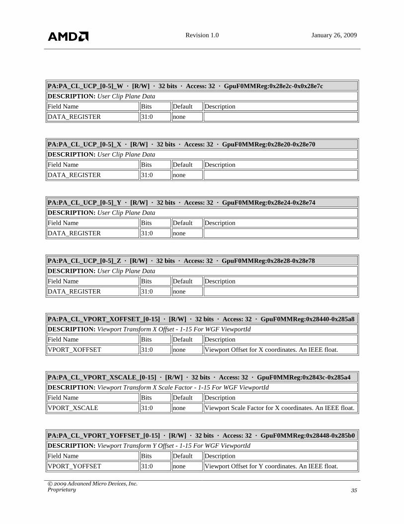
PA:PA_CL_UCP_[0-5]_W · [R/W] · 32 bits · Access: 32 · GpuF0MMReg:0x28e2c-0x0x28e7c
DESCRIPTION: User Clip Plane Data
Field Name Bits Default Description
DATA_REGISTER 31:0 none
PA:PA_CL_UCP_[0-5]_X · [R/W] · 32 bits · Access: 32 · GpuF0MMReg:0x28e20-0x28e70
DESCRIPTION: User Clip Plane Data
Field Name Bits Default Description
DATA_REGISTER 31:0 none
PA:PA_CL_UCP_[0-5]_Y · [R/W] · 32 bits · Access: 32 · GpuF0MMReg:0x28e24-0x28e74
DESCRIPTION: User Clip Plane Data
Field Name Bits Default Description
DATA_REGISTER 31:0 none
PA:PA_CL_UCP_[0-5]_Z · [R/W] · 32 bits · Access: 32 · GpuF0MMReg:0x28e28-0x28e78
DESCRIPTION: User Clip Plane Data
Field Name Bits Default Description
DATA_REGISTER 31:0 none
PA:PA_CL_VPORT_XOFFSET_[0-15] · [R/W] · 32 bits · Access: 32 · GpuF0MMReg:0x28440-0x285a8
DESCRIPTION: Viewport Transform X Offset - 1-15 For WGF ViewportId
Field Name Bits Default Description
VPORT_XOFFSET 31:0 none Viewport Offset for X coordinates. An IEEE float.
PA:PA_CL_VPORT_XSCALE_[0-15] · [R/W] · 32 bits · Access: 32 · GpuF0MMReg:0x2843c-0x285a4
DESCRIPTION: Viewport Transform X Scale Factor - 1-15 For WGF ViewportId
Field Name Bits Default Description
VPORT_XSCALE 31:0 none Viewport Scale Factor for X coordinates. An IEEE float.
PA:PA_CL_VPORT_YOFFSET_[0-15] · [R/W] · 32 bits · Access: 32 · GpuF0MMReg:0x28448-0x285b0
DESCRIPTION: Viewport Transform Y Offset - 1-15 For WGF ViewportId
Field Name Bits Default Description
VPORT_YOFFSET 31:0 none Viewport Offset for Y coordinates. An IEEE float.

Revision 1.0 January 26, 2009
© 2009 Advanced Micro Devices, Inc. Proprietary 36
PA:PA_CL_VPORT_YSCALE_[0-15] · [R/W] · 32 bits · Access: 32 · GpuF0MMReg:0x28444-0x285ac
DESCRIPTION: Viewport Transform Y Scale Factor - 1-15 For WGF ViewportId
Field Name Bits Default Description
VPORT_YSCALE 31:0 none Viewport Scale Factor for Y coordinates. An IEEE float.
PA:PA_CL_VPORT_ZOFFSET_[0-15] · [R/W] · 32 bits · Access: 32 · GpuF0MMReg:0x28450-0x285b8
DESCRIPTION: Viewport Transform Z Offset - 1-15 For WGF ViewportId
Field Name Bits Default Description
VPORT_ZOFFSET 31:0 none Viewport Offset for Z coordinates. An IEEE float.
PA:PA_CL_VPORT_ZSCALE_[0-15] · [R/W] · 32 bits · Access: 32 · GpuF0MMReg:0x2844c-0x285b4
DESCRIPTION: Viewport Transform Z Scale Factor - 1-15 For WGF ViewportId
Field Name Bits Default Description
VPORT_ZSCALE 31:0 none Viewport Scale Factor for Z coordinates. An IEEE float.
PA:PA_CL_VS_OUT_CNTL · [R/W] · 32 bits · Access: 32 · GpuF0MMReg:0x2881c
DESCRIPTION: Vertex Shader Output Control
Field Name Bits Default Description
CLIP_DIST_ENA_0 0 none Enable ClipDistance# to be used for user-defined
clipping. Requires VS_OUT_CCDIST#_ENA to be
set.
CLIP_DIST_ENA_1 1 none Enable ClipDistance# to be used for user-defined
clipping. Requires VS_OUT_CCDIST#_ENA to be
set.
CLIP_DIST_ENA_2 2 none Enable ClipDistance# to be used for user-defined
clipping. Requires VS_OUT_CCDIST#_ENA to be
set.
CLIP_DIST_ENA_3 3 none Enable ClipDistance# to be used for user-defined
clipping. Requires VS_OUT_CCDIST#_ENA to be
set.
CLIP_DIST_ENA_4 4 none Enable ClipDistance# to be used for user-defined
clipping. Requires VS_OUT_CCDIST#_ENA to be
set.
CLIP_DIST_ENA_5 5 none Enable ClipDistance# to be used for user-defined
clipping. Requires VS_OUT_CCDIST#_ENA to be
set.
CLIP_DIST_ENA_6 6 none Enable ClipDistance# to be used for user-defined
clipping. Requires VS_OUT_CCDIST#_ENA to be
set.
CLIP_DIST_ENA_7 7 none Enable ClipDistance# to be used for user-defined
Revision 1.0 January 26, 2009
© 2009 Advanced Micro Devices, Inc. Proprietary 37
clipping. Requires VS_OUT_CCDIST#_ENA to be
set.
CULL_DIST_ENA_0 8 none Enable CullDistance# to be used for user-defined clip
discard. Requires VS_OUT_CCDIST#_ENA to be set.
If all verts of a primitive are outside (culldist<0), then
primitive is discarded, else just let through (i.e. NOT
clipped).
CULL_DIST_ENA_1 9 none Enable CullDistance# to be used for user-defined clip
discard. Requires VS_OUT_CCDIST#_ENA to be set.
If all verts of a primitive are outside (culldist<0), then
primitive is discarded, else just let through (i.e. NOT
clipped).
CULL_DIST_ENA_2 10 none Enable CullDistance# to be used for user-defined clip
discard. Requires VS_OUT_CCDIST#_ENA to be set.
If all verts of a primitive are outside (culldist<0), then
primitive is discarded, else just let through (i.e. NOT
clipped).
CULL_DIST_ENA_3 11 none Enable CullDistance# to be used for user-defined clip
discard. Requires VS_OUT_CCDIST#_ENA to be set.
If all verts of a primitive are outside (culldist<0), then
primitive is discarded, else just let through (i.e. NOT
clipped).
CULL_DIST_ENA_4 12 none Enable CullDistance# to be used for user-defined clip
discard. Requires VS_OUT_CCDIST#_ENA to be set.
If all verts of a primitive are outside (culldist<0), then
primitive is discarded, else just let through (i.e. NOT
clipped).
CULL_DIST_ENA_5 13 none Enable CullDistance# to be used for user-defined clip
discard. Requires VS_OUT_CCDIST#_ENA to be set.
If all verts of a primitive are outside (culldist<0), then
primitive is discarded, else just let through (i.e. NOT
clipped).
CULL_DIST_ENA_6 14 none Enable CullDistance# to be used for user-defined clip
discard. Requires VS_OUT_CCDIST#_ENA to be set.
If all verts of a primitive are outside (culldist<0), then
primitive is discarded, else just let through (i.e. NOT
clipped).
CULL_DIST_ENA_7 15 none Enable CullDistance# to be used for user-defined clip
discard. Requires VS_OUT_CCDIST#_ENA to be set.
If all verts of a primitive are outside (culldist<0), then
primitive is discarded, else just let through (i.e. NOT
clipped).
USE_VTX_POINT_SIZE 16 none Use the PointSize output from the VS (in the x channel
of VS_OUT_MISC_VEC).
USE_VTX_EDGE_FLAG 17 none Use the EdgeFlag output from the VS (in the y channel
of VS_OUT_MISC_VEC).
USE_VTX_RENDER_TARGET_INDX 18 none Use the RenderTargetArrayIndx output from the VS
(in the z channel of VS_OUT_MISC_VEC). Only
valid for WGF Geometry Shader

Revision 1.0 January 26, 2009
© 2009 Advanced Micro Devices, Inc. Proprietary 38
USE_VTX_VIEWPORT_INDX 19 none Use the ViewportArrayIndx output from the VS (in the
w channel of VS_OUT_MISC_VEC). Only valid for
WGF Geometry Shader
USE_VTX_KILL_FLAG 20 none Use the KillFlag output from the VS (in the z channel
of VS_OUT_MISC_VEC). Mutually exclusive from
RTarrayindx
VS_OUT_MISC_VEC_ENA 21 none Output the VS output misc vector from the VS (SX) to
the PA (primitive assembler). Should be set if any of
the fields are to be used
VS_OUT_CCDIST0_VEC_ENA 22 none Output the VS output ccdist0 vector from the VS (SX)
to the PA (primitive assembler). Should be set if any of
the fields are to be used
VS_OUT_CCDIST1_VEC_ENA 23 none Output the VS output ccdist1 vector from the VS (SX)
to the PA (primitive assembler). Should be set if any of
the fields are to be used
PA:PA_CL_VTE_CNTL · [R/W] · 32 bits · Access: 32 · GpuF0MMReg:0x28818
DESCRIPTION: Viewport Transform Engine Control
Field Name Bits Default Description
VPORT_X_SCALE_ENA 0 none Viewport Transform Scale Enable for X component
VPORT_X_OFFSET_ENA 1 none Viewport Transform Offset Enable for X component
VPORT_Y_SCALE_ENA 2 none Viewport Transform Scale Enable for Y component
VPORT_Y_OFFSET_ENA 3 none Viewport Transform Offset Enable for Y component
VPORT_Z_SCALE_ENA 4 none Viewport Transform Scale Enable for Z component
VPORT_Z_OFFSET_ENA 5 none Viewport Transform Offset Enable for Z component
VTX_XY_FMT 8 none Indicates that the incoming X, Y have already been
multiplied by 1/W0.
If OFF, the Setup Engine will multiply the X, Y
coordinates by 1/W0.,
VTX_Z_FMT 9 none Indicates that the incoming Z has already been multiplied
by 1/W0.
If OFF, the Setup Engine will multiply the Z coordinate
by 1/W0.
VTX_W0_FMT 10 none Indicates that the incoming W0 is not 1/W0.
If ON, the Setup Engine will perform the reciprocal to
get 1/W0.
PERFCOUNTER_REF 11 none Indicates perf counters should increment for this context.
PA:PA_SC_AA_CONFIG · [R/W] · 32 bits · Access: 32 · GpuF0MMReg:0x28c04
DESCRIPTION: Multisample Antialiasing Control
Field Name Bits Default Description
MSAA_NUM_SAMPLES 1:0 none Specifies the number of samples to use for MSAA.
Representative of size of surface allocated for Color and
Revision 1.0 January 26, 2009
© 2009 Advanced Micro Devices, Inc. Proprietary 39
Depth. 0 = 1-sample, 1 = 2-sample, 2 = 4-sample, 3 = 8-
sample.
AA_MASK_CENTROID_DTMN 4 none Specifies whether to apply the MSAA Mask before or
after the centroid determination. 0 = before; 1 = after.
MAX_SAMPLE_DIST 16:13 none Specifies the maximum distance (in subpixels) between
the pixel center and the outermost subpixel sample. This
value is used to optimize coarse walk and quad identity.
Should be set to 0 when not anti-aliasing. Max value for
R600 should be 8(16ths).
PA:PA_SC_AA_MASK · [R/W] · 32 bits · Access: 32 · GpuF0MMReg:0x28c48
DESCRIPTION: Multisample AA Mask
Field Name Bits Default Description
AA_MASK 31:0 none This mask is used for Multisample AA. It contains 4 8-
bit masks. The 4 masks are applied to each 2x2 screen-
aligned pixels as follows: ULC 7:0, URC 15:8, LLC
23:16, LRC 31:24, LSB is Sample0, MSB is Sample7.
PA:PA_SC_AA_SAMPLE_LOCS_2S · [R/W] · 32 bits · Access: 32 · GpuF0MMReg:0x8b40
DESCRIPTION: Multi-Sample Programmable Sample Locations for 2-Sample - Used by SC & CB`s
Field Name Bits Default Description
S0_X 3:0 none 4b signed offset from pixel center. Range -8/16 to 7/16.
S0_Y 7:4 none 4b signed offset from pixel center. Range -8/16 to 7/16.
S1_X 11:8 none 4b signed offset from pixel center. Range -8/16 to 7/16.
S1_Y 15:12 none 4b signed offset from pixel center. Range -8/16 to 7/16.
PA:PA_SC_AA_SAMPLE_LOCS_4S · [R/W] · 32 bits · Access: 32 · GpuF0MMReg:0x8b44
DESCRIPTION: Multi-Sample Programmable Sample Locations for 4-Sample - Used by SC & CB`s
Field Name Bits Default Description
S0_X 3:0 none 4b signed offset from pixel center. Range -8/16 to 7/16.
S0_Y 7:4 none 4b signed offset from pixel center. Range -8/16 to 7/16.
S1_X 11:8 none 4b signed offset from pixel center. Range -8/16 to 7/16.
S1_Y 15:12 none 4b signed offset from pixel center. Range -8/16 to 7/16.
S2_X 19:16 none 4b signed offset from pixel center. Range -8/16 to 7/16.
S2_Y 23:20 none 4b signed offset from pixel center. Range -8/16 to 7/16.
S3_X 27:24 none 4b signed offset from pixel center. Range -8/16 to 7/16.
S3_Y 31:28 none 4b signed offset from pixel center. Range -8/16 to 7/16.
PA:PA_SC_AA_SAMPLE_LOCS_8S_WD0 · [R/W] · 32 bits · Access: 32 · GpuF0MMReg:0x8b48

Revision 1.0 January 26, 2009
© 2009 Advanced Micro Devices, Inc. Proprietary 40
DESCRIPTION: Multi-Sample Programmable Sample Locations for 8-Sample First Word - Used by SC & CB`s
Field Name Bits Default Description
S0_X 3:0 none 4b signed offset from pixel center. Range -8/16 to 7/16.
S0_Y 7:4 none 4b signed offset from pixel center. Range -8/16 to 7/16.
S1_X 11:8 none 4b signed offset from pixel center. Range -8/16 to 7/16.
S1_Y 15:12 none 4b signed offset from pixel center. Range -8/16 to 7/16.
S2_X 19:16 none 4b signed offset from pixel center. Range -8/16 to 7/16.
S2_Y 23:20 none 4b signed offset from pixel center. Range -8/16 to 7/16.
S3_X 27:24 none 4b signed offset from pixel center. Range -8/16 to 7/16.
S3_Y 31:28 none 4b signed offset from pixel center. Range -8/16 to 7/16.
PA:PA_SC_AA_SAMPLE_LOCS_8S_WD1 · [R/W] · 32 bits · Access: 32 · GpuF0MMReg:0x8b4c
DESCRIPTION: Multi-Sample Programmable Sample Locations for 8-Sample Second Word - Used by SC & CB`s
Field Name Bits Default Description
S4_X 3:0 none 4b signed offset from pixel center. Range -8/16 to 7/16.
S4_Y 7:4 none 4b signed offset from pixel center. Range -8/16 to 7/16.
S5_X 11:8 none 4b signed offset from pixel center. Range -8/16 to 7/16.
S5_Y 15:12 none 4b signed offset from pixel center. Range -8/16 to 7/16.
S6_X 19:16 none 4b signed offset from pixel center. Range -8/16 to 7/16.
S6_Y 23:20 none 4b signed offset from pixel center. Range -8/16 to 7/16.
S7_X 27:24 none 4b signed offset from pixel center. Range -8/16 to 7/16.
S7_Y 31:28 none 4b signed offset from pixel center. Range -8/16 to 7/16.
PA:PA_SC_AA_SAMPLE_LOCS_8S_WD1_MCTX · [R/W] · 32 bits · Access: 32 ·
GpuF0MMReg:0x28c20
DESCRIPTION: Multi-Sample Programmable Sample Locations for 8-Sample Second Word - Used by SC, SPI &
CB`s
Field Name Bits Default Description
S4_X 3:0 none 4b signed offset from pixel center. Range -8/16 to 7/16.
S4_Y 7:4 none 4b signed offset from pixel center. Range -8/16 to 7/16.
S5_X 11:8 none 4b signed offset from pixel center. Range -8/16 to 7/16.
S5_Y 15:12 none 4b signed offset from pixel center. Range -8/16 to 7/16.
S6_X 19:16 none 4b signed offset from pixel center. Range -8/16 to 7/16.
S6_Y 23:20 none 4b signed offset from pixel center. Range -8/16 to 7/16.
S7_X 27:24 none 4b signed offset from pixel center. Range -8/16 to 7/16.
S7_Y 31:28 none 4b signed offset from pixel center. Range -8/16 to 7/16.
PA:PA_SC_AA_SAMPLE_LOCS_MCTX · [R/W] · 32 bits · Access: 32 · GpuF0MMReg:0x28c1c

Revision 1.0 January 26, 2009
© 2009 Advanced Micro Devices, Inc. Proprietary 41
DESCRIPTION: Multi-Sample Programmable Sample Locations for 2-Sample, 4-Sample, 8-Sample First Word -
Used by SC, SPI & CB`s
Field Name Bits Default Description
S0_X 3:0 none 4b signed offset from pixel center. Range -8/16 to 7/16.
S0_Y 7:4 none 4b signed offset from pixel center. Range -8/16 to 7/16.
S1_X 11:8 none 4b signed offset from pixel center. Range -8/16 to 7/16.
S1_Y 15:12 none 4b signed offset from pixel center. Range -8/16 to 7/16.
S2_X 19:16 none 4b signed offset from pixel center. Range -8/16 to 7/16.
S2_Y 23:20 none 4b signed offset from pixel center. Range -8/16 to 7/16.
S3_X 27:24 none 4b signed offset from pixel center. Range -8/16 to 7/16.
S3_Y 31:28 none 4b signed offset from pixel center. Range -8/16 to 7/16.
PA:PA_SC_CLIPRECT_[0-3]_BR · [R/W] · 32 bits · Access: 32 · GpuF0MMReg:0x28214-0x2822c
DESCRIPTION: Clip Rectangle Bottom-Right Specification
Field Name Bits Default Description
BR_X 13:0 none Right x value of clip rectangle. 14 bits unsigned. Valid
range 0-8192. Exclusive for BOTTOM_RIGHT
BR_Y 29:16 none Bottom y value of clip rectangle. 14 bits unsigned. Valid
range 0-8192. Exclusive for BOTTOM_RIGHT
PA:PA_SC_CLIPRECT_[0-3]_TL · [R/W] · 32 bits · Access: 32 · GpuF0MMReg:0x28210-0x28228
DESCRIPTION: Clip Rectangle Top-Left Specification
Field Name Bits Default Description
TL_X 13:0 none Left x value of clip rectangle. 14 bits unsigned. Valid
range 0-8191. Inclusive for UPPER_LEFT
TL_Y 29:16 none Top y value of clip rectangle. 14 bits unsigned. Valid
range 0-8191. Inclusive for UPPER_LEFT
PA:PA_SC_CLIPRECT_RULE · [R/W] · 32 bits · Access: 32 · GpuF0MMReg:0x2820c
DESCRIPTION: OpenGL Clip boolean function
Field Name Bits Default Description
CLIP_RULE 15:0 none OpenGL Clip boolean function. The `inside` flags for
each of the four clip rectangles form a 4-bit binary
number. The corresponding bit in this 16-bit number
specifies whether the pixel is visible.
PA:PA_SC_CNTL_STATUS · [R] · 32 bits · Access: 32 · GpuF0MMReg:0x8be0
DESCRIPTION: Status Bits
Field Name Bits Default Description

Revision 1.0 January 26, 2009
© 2009 Advanced Micro Devices, Inc. Proprietary 42
MPASS_OVERFLOW 30 none If set, the Multipass Pixel Shader SC 32-bit PV counter
overflowed. This bit is reset when register is read
PA:PA_SC_ENHANCE · [R/W] · 32 bits · Access: 32 · GpuF0MMReg:0x8bf0
DESCRIPTION: Used for Late Additions of Control Bits
Field Name Bits Default Description
FORCE_EOV_MAX_CLK_CNT 11:0 none Cycle count used to determine when to force out a pixel
vector prematurely
FORCE_EOV_MAX_TILE_CNT 23:12 none Tile count used to determine when to force out a pixel
vector prematurely
PA:PA_SC_GENERIC_SCISSOR_BR · [R/W] · 32 bits · Access: 32 · GpuF0MMReg:0x28244
DESCRIPTION: Generic Scissor rectangle specification. Scissor is conditionally (See
WINDOW_OFFSET_ENABLE) offset by WINDOW_OFFSET.
Field Name Bits Default Description
BR_X 13:0 none Right hand edge of scissor rectangle. 14 bits unsigned.
Valid range 0-8192. Exclusive for BOTTOM_RIGHT.
BR_Y 29:16 none Lower edge of scissor rectangle. 14 bits unsigned. Valid
range 0-8192. Exclusive for BOTTOM_RIGHT.
PA:PA_SC_GENERIC_SCISSOR_TL · [R/W] · 32 bits · Access: 32 · GpuF0MMReg:0x28240
DESCRIPTION: Generic Scissor rectangle specification. Scissor is conditionally (See
WINDOW_OFFSET_ENABLE) offset by WINDOW_OFFSET.
Field Name Bits Default Description
TL_X 13:0 none Left hand edge of scissor rectangle. 14-bits unsigned.
Valid range 0-8191. Inclusive for UPPER_LEFT.
TL_Y 29:16 none Upper edge of scissor rectangle. 14-bits unsigned. Valid
range 0-8191. Inclusive for UPPER_LEFT.
WINDOW_OFFSET_DISABLE 31 none If set, generic scissor is not offset by the
WINDOW_OFFSET register values.
PA:PA_SC_LINE_CNTL · [R/W] · 32 bits · Access: 32 · GpuF0MMReg:0x28c00
DESCRIPTION: Line Drawing Control
Field Name Bits Default Description
BRES_CNTL 7:0 none This field indicates what the hardware should do on the
minor axis of the line, when the line is exactly half way
between two pixels (bresenham error = 0). This field is a
LUT (BRES_CNTL[7:0] w/ 1-bit per entry, where if the
bit BRES_CNTL[index] = `1` then that means to step the
minor axis. The 3-bit index is calculated from the
attributes of the line ((abs(Xend - Xstart) >= abs(Yend -

Revision 1.0 January 26, 2009
© 2009 Advanced Micro Devices, Inc. Proprietary 43
Ystart)) << 2) | ((Xstart <= Xend) << 1) | (Ystart <=
Yend)
USE_BRES_CNTL 8 none If set, use the bresenham control field. Should be set for
2D lines, clear for 3D lines.
EXPAND_LINE_WIDTH 9 none If set, the line width will be expanded by the 1/cos(a)
where a the minimum angle from horz or vertical. This
bit most likely should be set whenever MSAA_ENABLE
is set or Line Antialiasing is being done in pixel shader.
LAST_PIXEL 10 none If set the last pixel of a line will not be killed by the
diamond exit rule.
PA:PA_SC_LINE_STIPPLE · [R/W] · 32 bits · Access: 32 · GpuF0MMReg:0x28a0c
DESCRIPTION: Line Stipple Control
Field Name Bits Default Description
LINE_PATTERN 15:0 none 16-bit pattern
REPEAT_COUNT 23:16 none Pattern bit repeat count (minus 1). Field has a valid range
of 0-255 which maps to OGL api values of 1-256.
PATTERN_BIT_ORDER 28 none Bit Ordering of Pattern Bits:
0 = Little Bit Order,
1 = Big Bit Order
AUTO_RESET_CNTL 30:29 none Auto reset control of current pattern count/pointer.
0 = Never reset current pattern count/pointer.
1 = Reset current pattern count/pointer at each primitive
(line list).
2 = Reset current pattern count/pointer at each packet
(line strip).
PA:PA_SC_LINE_STIPPLE_STATE · [R/W] · 32 bits · Access: 32 · GpuF0MMReg:0x8b10
DESCRIPTION: Current values for Line Stipple
Field Name Bits Default Description
CURRENT_PTR 3:0 none Indicates current state of pattern pointer (can be set w/ a
register write).
CURRENT_COUNT 15:8 none Current state of the repeat counter (can be set w/a
register write).
PA:PA_SC_MODE_CNTL · [R/W] · 32 bits · Access: 32 · GpuF0MMReg:0x28a4c
DESCRIPTION: SC Mode Control Register for Various Enables
Field Name Bit
s
Defaul
t Description
MSAA_ENABLE 0 none Enable MultiSample AA. If set, the
MSAA_NUM_SAMPLES+1 used for MSAA will have
unique subpixel locations as described below and
MSAA_NUM_SAMPLES must not equal 0. If clear, all

Revision 1.0 January 26, 2009
© 2009 Advanced Micro Devices, Inc. Proprietary 44
MSAA_NUM_SAMPLES+1 will be sampled using the
pixel center
All sample locations are specified as an offset from pixel
cetner.
2 SAMPLE Sample 0: -4, 4
Sample 1: 4, -4
4 SAMPLE Sample 0: -2, -2
Sample 1: 2, 2
Sample 2: -6, 6
Sample 3: 6, -6
8 SAMPLE Sample 0: -2, -5
Sample 1: 4, -4
Sample 2: 1, 6
Sample 3: -6, -2
Sample 4: 6, 1
Sample 5: 0, 0
Sample 6: -5, 4
Sample 7: 7, -8
CLIPRECT_ENABLE 1 none Enables 4 cliprects (same as setting CLIPRECT_RULE to
0xffff)
LINE_STIPPLE_ENABLE 2 none Enable line stipple processing
MULTI_CHIP_PRIM_DISCARD_ENAB
LE
3 none Enables primitives to be discarded based on
PA_SC_MULTI_CHIP_CNTL. Should be disabled for
stippled lines even when in Multi-Chip mode
WALK_ORDER_ENABLE 4 none Enables fixed pattern for quad walk order. Must be
disabled for overlapping blit rendering.
HALVE_DETAIL_SAMPLE_PERF 5 none Enables the ability to halve the performance of the detail
samplers in all MSAA modes.
WALK_SIZE 6 none Defines the size of the SC walk stamp. 0 : walk by
supertiles (32 bits); 1 : walk by tiles (8 bits).
WALK_ALIGNMENT 7 none Defines the alignment value of the SC walker. 0 : align by
supertiles (32 bits); 1 : align by tiles (8 bits).
WALK_ALIGN8_PRIM_FITS_ST 8 none When alignment value is set to supertiles (32 bits), enables
the walker to align by tiles (8 bits) if primitive fits within
one supertile.
TILE_COVER_NO_SCISSOR 9 none Disables the use of scissors when determining tile covered.
KILL_PIX_POST_HI_Z 10 none If set, all pixels are killed in the SC after the HI-Z test.
Typically set for VizQuery geometry
KILL_PIX_POST_DETAIL_MASK 11 none If set, all pixels are killed in the SC after the detail mask.
Can be used for performance info
MULTI_CHIP_SUPERTILE_ENABLE 12 none Enables Multi-Chip supertile mode with the configuration
defined in PA_SC_MULTI_CHIP_CNTL.
TILE_COVER_DISABLE 13 none Disables tile covered (Hi-Z optimization) that is sent to the
DBs.
FORCE_EOV_CNTDWN_ENABLE 14 none Enables forcing out pixel vectors prematurely based on the
cycle count programmed in
PA_SC_ENHANCE::FORCE_EOV_MAX_CLK_CNT[11
:0]

Revision 1.0 January 26, 2009
© 2009 Advanced Micro Devices, Inc. Proprietary 45
FORCE_EOV_TILE_ENABLE 15 none Enables forcing out pixel vectors prematurely based on the
tile count programmed in
PA_SC_ENHANCE::FORCE_EOV_MAX_TILE_CNT[1
1:0]
FORCE_EOV_REZ_ENABLE 16 none Enables forcing out pixel vectors prematurely based on the
ReZ hang condition(ie. cache locked) detected in the DB
PS_ITER_SAMPLE 17 none Enables per-sample (i.e. unique shader-computed value per
sample) pixel shader execution.
PA:PA_SC_MPASS_PS_CNTL · [R/W] · 32 bits · Access: 32 · GpuF0MMReg:0x28a48
DESCRIPTION: Multi-Pass Pixel Shader Control Register
Field Name Bits Default Description
MPASS_PIX_VEC_PER_PASS 19:0 none Specifies the number of pixel vectors to process for each
pass. Should be based on the amount of memory
available for pixel shader export to memory and size of
each pixels output data. Note there are 64 pixels per pixel
vector in R600. There will likely be 32 pixels /pixel
vector and 16 in derivative parts
MPASS_PS_ENA 31 none If set, enables multipass pixel shader operation.
PA:PA_SC_MULTI_CHIP_CNTL · [R/W] · 32 bits · Access: 32 · GpuF0MMReg:0x8b20
DESCRIPTION: Controls the Screen Divisioning for Multi-Chip Configurations
Field Name Bits Default Description
LOG2_NUM_CHIPS 2:0 none Log2 of the number of chips in the multi-chip
configuration.
MULTI_CHIP_TILE_SIZE 4:3 none Size of the tile per chip within each super-tile.
POSSIBLE VALUES:
00 - 16 x 16 pixel tile per chip.
01 - 32 x 32 pixel tile per chip.
02 - 64 x 64 pixel tile per chip.
03 - 128x128 pixel tile per chip.
CHIP_TILE_X_LOC 7:5 none X Location of the chip within the super-tile.
CHIP_TILE_Y_LOC 10:8 none Y Location of the chip within the super-tile.
CHIP_SUPER_TILE_B 11 none Must be 0 for even LOG2_NUM_CHIPS. For odd
LOG2_NUM_CHIPS, this field specifies the second
super tile.
PA:PA_SC_SCREEN_SCISSOR_BR · [R/W] · 32 bits · Access: 32 · GpuF0MMReg:0x28034
DESCRIPTION: Screen Scissor rectangle specification. This scissor is NOT affected by WINDOW_OFFSET.
Negative numbers clamped to 0, so reads will mismatch on negative values.
Field Name Bits Default Description
BR_X 14:0 none Right hand edge of scissor rectangle. 15 bits signed.

Revision 1.0 January 26, 2009
© 2009 Advanced Micro Devices, Inc. Proprietary 46
Valid range -16K to 8192. Exclusive for
BOTTOM_RIGHT.
BR_Y 30:16 none Lower edge of scissor rectangle. 15 bits signed. Valid
range -16K to 8192. Exclusive for BOTTOM_RIGHT.
PA:PA_SC_SCREEN_SCISSOR_TL · [R/W] · 32 bits · Access: 32 · GpuF0MMReg:0x28030
DESCRIPTION: Screen Scissor rectangle specification. This scissor is NOT affected by WINDOW_OFFSET.
Negative numbers clamped to 0, so reads will mismatch on negative values.
Field Name Bits Default Description
TL_X 14:0 none Left hand edge of scissor rectangle. 15 bits signed. Valid
range -16K to 8191. Inclusive for UPPER_LEFT.
TL_Y 30:16 none Upper edge of scissor rectangle. 15 bits signed. Valid
range -16K to 8191. Inclusive for UPPER_LEFT.
PA:PA_SC_VPORT_SCISSOR_[0-15]_BR · [R/W] · 32 bits · Access: 32 · GpuF0MMReg:0x28254-
0x282cc
DESCRIPTION: WGF ViewportID Scissor rectangle specification(0-15). Scissor is conditionally (See
WINDOW_OFFSET_ENABLE) offset by WINDOW_OFFSET.
Field Name Bits Default Description
BR_X 13:0 none Right hand edge of scissor rectangle. 14 bits unsigned.
Valid range 0-8192. Exclusive for BOTTOM_RIGHT.
BR_Y 29:16 none Lower edge of scissor rectangle. 14 bits unsigned. Valid
range 0-8192. Exclusive for BOTTOM_RIGHT.
PA:PA_SC_VPORT_SCISSOR_[0-15]_TL · [R/W] · 32 bits · Access: 32 · GpuF0MMReg:0x28250-
0x282c8
DESCRIPTION: WGF ViewportId Scissor rectangle specification(0-15). Scissor is conditionally (See
WINDOW_OFFSET_ENABLE) offset by WINDOW_OFFSET.
Field Name Bits Default Description
TL_X 13:0 none Left hand edge of scissor rectangle. 14-bits unsigned.
Valid range 0-8191. Inclusive for UPPER_LEFT.
TL_Y 29:16 none Upper edge of scissor rectangle. 14-bits unsigned. Valid
range 0-8191. Inclusive for UPPER_LEFT.
WINDOW_OFFSET_DISABLE 31 none If set, viewportId scissor is not offset by the
WINDOW_OFFSET register values.
PA:PA_SC_VPORT_ZMAX_[0-15] · [R/W] · 32 bits · Access: 32 · GpuF0MMReg:0x282d4-0x2834c
DESCRIPTION: Viewport Transform Z Max Clamp - 0-15 For WGF ViewportId
Field Name Bits Default Description
VPORT_ZMAX 31:0 none Maximum Z Value from Viewport Transform. Z values
will be clamped by the DB to this value.

Revision 1.0 January 26, 2009
© 2009 Advanced Micro Devices, Inc. Proprietary 47
PA:PA_SC_VPORT_ZMIN_[0-15] · [R/W] · 32 bits · Access: 32 · GpuF0MMReg:0x282d0-0x28348
DESCRIPTION: Viewport Transform Z Min Clamp - 0-15 For WGF ViewportId
Field Name Bits Default Description
VPORT_ZMIN 31:0 none Minimum Z Value from Viewport Transform. Z values
will be clamped by the DB to this value.
PA:PA_SC_WINDOW_OFFSET · [R/W] · 32 bits · Access: 32 · GpuF0MMReg:0x28200
DESCRIPTION: Offset from screen coords to window coords. Vertices will be offset by these values if
PA_SU_SC_MODE_CNTL.VTX_WINDOW_OFFSET_ENABLE is et. The WINDOW_SCISSOR will be offset by
these values if the WINDOW_SCISSOR_TL.WINDOW_OFFSET_DISABLE is clear. If this value allows the window
to extend beyond the Front Buffer (Surface) dimensions, it is expected that the SCREEN_SCISSOR is used to limit to
FB surface.
Field Name Bits Default Description
WINDOW_X_OFFSET 14:0 none Offset in x-direction from screen to window coords. 16-
bit 2`s comp signed value. Valid Range +/- 16K.
WINDOW_Y_OFFSET 30:16 none Offset in y-direction from screen to window coords. 16-
bit 2`s comp signed value. Valid Range +/- 16K.
PA:PA_SC_WINDOW_SCISSOR_BR · [R/W] · 32 bits · Access: 32 · GpuF0MMReg:0x28208
DESCRIPTION: Window Scissor rectangle specification. Scissor is conditionally (See
WINDOW_OFFSET_ENABLE) offset by WINDOW_OFFSET.
Field Name Bits Default Description
BR_X 13:0 none Right hand edge of scissor rectangle. 14 bits unsigned.
Valid range 0-8192. Exclusive for BOTTOM_RIGHT.
BR_Y 29:16 none Lower edge of scissor rectangle. 14 bits unsigned. Valid
range 0-8192. Exclusive for BOTTOM_RIGHT.
PA:PA_SC_WINDOW_SCISSOR_TL · [R/W] · 32 bits · Access: 32 · GpuF0MMReg:0x28204
DESCRIPTION: Window Scissor rectangle specification. Scissor is conditionally (See
WINDOW_OFFSET_ENABLE) offset by WINDOW_OFFSET.
Field Name Bits Default Description
TL_X 13:0 none Left hand edge of scissor rectangle. 14-bits unsigned.
Valid range 0-8191. Inclusive for UPPER_LEFT.
TL_Y 29:16 none Upper edge of scissor rectangle. 14-bits unsigned. Valid
range 0-8191. Inclusive for UPPER_LEFT.
WINDOW_OFFSET_DISABLE 31 none If set, window scissor is not offset by the
WINDOW_OFFSET register values.
PA:PA_SU_CNTL_STATUS · [R] · 32 bits · Access: 32 · GpuF0MMReg:0x8a50

Revision 1.0 January 26, 2009
© 2009 Advanced Micro Devices, Inc. Proprietary 48
DESCRIPTION: Status Bits
Field Name Bits Default Description
SU_BUSY 31 none Busy Status Bit
PA:PA_SU_LINE_CNTL · [R/W] · 32 bits · Access: 32 · GpuF0MMReg:0x28a08
DESCRIPTION: Line control
Field Name Bits Default Description
WIDTH 15:0 none 1/2 width of line, in subpixels; (16.0) fixed format.
PA:PA_SU_POINT_MINMAX · [R/W] · 32 bits · Access: 32 · GpuF0MMReg:0x28a04
DESCRIPTION: Specifies maximum and minimum point & sprite sizes for per vertex size specification.
Field Name Bits Default Description
MIN_SIZE 15:0 none Minimum point & sprite radius size to allow. fixed point
(12.4), 12 bits integer, 4 bits fractional pixels
MAX_SIZE 31:16 none Maximum point & sprite radius size to allow. fixed point
(12.4), 12 bits integer, 4 bits fractional pixels
PA:PA_SU_POINT_SIZE · [R/W] · 32 bits · Access: 32 · GpuF0MMReg:0x28a00
DESCRIPTION: Dimensions for Points
Field Name Bits Default Description
HEIGHT 15:0 none 1/2 Height (Vertical Radius) of point; fixed (12.4), 12
bits integer, 4 bits fractional pixels.
WIDTH 31:16 none 1/2 Width (Horizontal Radius)of point; fixed (12.4), 12
bits integer, 4 bits fractional pixels.
PA:PA_SU_POLY_OFFSET_BACK_OFFSET · [R/W] · 32 bits · Access: 32 · GpuF0MMReg:0x28e0c
DESCRIPTION: Back-Facing Polygon Offset Offset
Field Name Bits Default Description
OFFSET 31:0 none Specifies polygon offset offset for back-facing polygons;
32b IEEE fixed format.
PA:PA_SU_POLY_OFFSET_BACK_SCALE · [R/W] · 32 bits · Access: 32 · GpuF0MMReg:0x28e08
DESCRIPTION: Back-Facing Polygon Offset Scale
Field Name Bits Default Description
SCALE 31:0 none Specifies polygon offset scale for back-facing polygons;
32-bit IEEE float format.

Revision 1.0 January 26, 2009
© 2009 Advanced Micro Devices, Inc. Proprietary 49
PA:PA_SU_POLY_OFFSET_CLAMP · [R/W] · 32 bits · Access: 32 · GpuF0MMReg:0x28dfc
DESCRIPTION: Clamp Value for Polygon Offset
Field Name Bits Default Description
CLAMP 31:0 none Specifies the maximum (if clamp is positive) or
minimum (if clamp is negative) value clamp for the
polygon offset result.
PA:PA_SU_POLY_OFFSET_DB_FMT_CNTL · [R/W] · 32 bits · Access: 32 · GpuF0MMReg:0x28df8
DESCRIPTION: Polygon Offset Depth Buffer Format Control
Field Name Bits Default Description
POLY_OFFSET_NEG_NUM_DB_BITS 7:0 none Specifies the number of bits in the depth buffer format.
Specified as a negative value typically. For fixed point
formats, should be number of bits (i.e. -16, -24), for
float formats should be number of mantissa bits (i.e. -
23). This is a signed 8b value, range -128,127
POLY_OFFSET_DB_IS_FLOAT_FMT 8 none Specifies whether the depth buffer format is fixed or
float. The NEG_NUM_DB_BITS is used differently
(i.e. different POLY_OFFSET equation for fixed vs.
float buffer formats.
PA:PA_SU_POLY_OFFSET_FRONT_OFFSET · [R/W] · 32 bits · Access: 32 · GpuF0MMReg:0x28e04
DESCRIPTION: Front-Facing Polygon Offset Offset
Field Name Bits Default Description
OFFSET 31:0 none Specifies polygon offset offset for front-facing polygons;
32b IEEE fixed format.
PA:PA_SU_POLY_OFFSET_FRONT_SCALE · [R/W] · 32 bits · Access: 32 · GpuF0MMReg:0x28e00
DESCRIPTION: Front-Facing Polygon Offset Scale
Field Name Bits Default Description
SCALE 31:0 none Specifies polygon offset scale for front-facing polygons;
32-bit IEEE float format.
PA:PA_SU_SC_MODE_CNTL · [R/W] · 32 bits · Access: 32 · GpuF0MMReg:0x28814
DESCRIPTION: SU/SC Controls for Facedness Culling, Polymode, Polygon Offset, and various Enables
Field Name Bits Default Description
CULL_FRONT 0 none Enable for front-face culling.
POSSIBLE VALUES:
00 - Do not cull front-facing triangles.
01 - Cull front-facing triangles.
CULL_BACK 1 none Enable for back-face culling.

Revision 1.0 January 26, 2009
© 2009 Advanced Micro Devices, Inc. Proprietary 50
POSSIBLE VALUES:
00 - Do not cull back-facing triangles.
01 - Cull back-facing triangles.
FACE 2 none X-Ored with cross product sign to determine positive
facing
POSSIBLE VALUES:
00 - Positive cross product is front (CCW).
01 - Negative cross product is front (CW).
POLY_MODE 4:3 none Polygon mode enable.
POSSIBLE VALUES:
00 - Disable poly mode (render triangles).
01 - Dual mode (send 2 sets of 3 polys with
specified poly type).
02 - Reserved
POLYMODE_FRONT_PTYPE 7:5 none Specifies how to render front-facing polygons.
POSSIBLE VALUES:
00 - Draw points.
01 - Draw lines.
02 - Draw triangles.
03 - Reserved 3 - 7.
POLYMODE_BACK_PTYPE 10:8 none Specifies how to render back-facing polygons.
POSSIBLE VALUES:
00 - Draw points.
01 - Draw lines.
02 - Draw triangles.
03 - Reserved 3 - 7.
POLY_OFFSET_FRONT_ENABLE 11 none Enables front facing polygon`s offset.
POSSIBLE VALUES:
00 - Disable front offset.
01 - Enable front offset.
POLY_OFFSET_BACK_ENABLE 12 none Enables back facing polygon`s offset.
POSSIBLE VALUES:
00 - Disable back offset.
01 - Enable back offset.
POLY_OFFSET_PARA_ENABLE 13 none Enables polygon offset for non-triangle primitives.
POSSIBLE VALUES:
00 - Disable front offset for parallelograms.
01 - Enable front offset for parallelograms.
VTX_WINDOW_OFFSET_ENABLE 16 none Enables addition of PA_SC_WINDOW_OFFSET
values to vertex data.

Revision 1.0 January 26, 2009
© 2009 Advanced Micro Devices, Inc. Proprietary 51
PROVOKING_VTX_LAST 19 none Defines which vertex of a primitive is used for attribute
components when flat shading is enabled
POSSIBLE VALUES:
00 - 0 = First Vtx (D3D)
01 - 1 = Last Vtx (OGL)
PERSP_CORR_DIS 20 none Disables perspective correction for all attributes
MULTI_PRIM_IB_ENA 21 none Enables multiple primitive sets to be placed in a single
index buffer, separated by RESET_INDX indices
PA:PA_SU_VTX_CNTL · [R/W] · 32 bits · Access: 32 · GpuF0MMReg:0x28c08
DESCRIPTION: Miscellaneous SU Control
Field Name Bits Default Description
PIX_CENTER 0 none Specifies where the pixel center of the incoming vertex
is. The drawing engine itself has pixel centers @ 0.5, so
if this bit is `0`, 0.5 will be added to the X,Y coordinates
to move the incoming vertex onto our internal grid.
POSSIBLE VALUES:
00 - 0 = Pixel Center @ 0.0 (D3D)
01 - 1 = Pixel Center @ 0.5 (OGL)
ROUND_MODE 2:1 none Controls conversion of X,Y coordinates from IEEE to
fixed-point
POSSIBLE VALUES:
00 - 0 = Truncate (OGL)
01 - 1 = Round
02 - 2 = Round to Even (D3D)
03 - 3 = Round to Odd
QUANT_MODE 5:3 none Controls conversion of X,Y coordinates from IEEE to
fixed-point
POSSIBLE VALUES:
00 - 0 = 1/16th
01 - 1 = 1/8th
02 - 2 = 1/4th
03 - 3 = 1/2
04 - 4 = 1
05 - 5 = 1/256th

Revision 1.0 January 26, 2009
© 2009 Advanced Micro Devices, Inc. Proprietary 52
3. General Shader Registers
SQ:SQ_CONFIG · [W] · 32 bits · Access: 32 · GpuF0MMReg:0x8c00
DESCRIPTION: (1-state) SQ config options. The graphics pipe must be idle to change these.
Field Name Bits Default Description
VC_ENABLE 0 0x0 Vertex Cache (VC) is present; set to zero to disable VC.
When VC is disabled, all vertex fetches go through the
TC rather than VC regardless of the instruction bit
which selects TC/VC.
EXPORT_SRC_C 1 0x0
DX9_CONSTS 2 0x0 DX9 constant file mode. (0 = dx10 constant cache
mode, 1 = dx9 constant file mode). This applies to all
shaders.
ALU_INST_PREFER_VECTOR 3 0x0 ALU clause instruction assignment. When a group of 4
or less instructions, there may be ambiguity whether to
assign the last instruction to the vector pipe (according
to the instruction`s dest-chan), or to the scalar pipe
(trans). This bit controls that decision: 0 = send the last
instruction word to the scalar (trans) pipe if possible, 1
= prefer to send it to the vector pipe. This bit is only
used when the decision is ambiguous (not ambiguous if:
a vector-only or trans-only opcode, or the last
instruction writes to the same dest-chan as another
instruction in the group. The shader-compiler must be
aware of this bit setting and compile accordingly.
Default is: 0 (prefer-scalar).
DX10_CLAMP 4 0x0 R600: DX10 clamp mode. (1 = dx10 mode, 0 = dx9
mode). This applies to all shaders. This affects how the
SP output clamp treats NaN. NOT USED IN R6XX
DERIVATIVES (see sq_pgm_resources_*)
ALU_PREFER_ONE_WATERFALL 5 0x0
ALU_MAX_ONE_WATERFALL 6 0x0
CLAUSE_SEQ_PRIO 9:8 0x0
PS_PRIO 25:24 0x0
VS_PRIO 27:26 0x0
GS_PRIO 29:28 0x0
ES_PRIO 31:30 0x0
SQ:SQ_ESGS_RING_BASE · [R/W] · 32 bits · Access: 32 · GpuF0MMReg:0x8c40
DESCRIPTION: (1-state) Memory base address of the ES->GS ring buffer (256-byte aligned)
Field Name Bits Default Description
MEM_BASE 31:0 0x0 Format is [39:8]
SQ:SQ_ESGS_RING_ITEMSIZE · [R/W] · 32 bits · Access: 32 · GpuF0MMReg:0x288a8

Revision 1.0 January 26, 2009
© 2009 Advanced Micro Devices, Inc. Proprietary 53
DESCRIPTION: (8-state) Space allocated to a single pixel/vertex in the ES->GS ring buffer (in DWORDs).
Itemsize is the true count, not count-1 and represents [0..32767] dwords.
Field Name Bits Default Description
ITEMSIZE 14:0 0x0 Format is [16:2]
SQ:SQ_ESGS_RING_SIZE · [R/W] · 32 bits · Access: 32 · GpuF0MMReg:0x8c44
DESCRIPTION: (1-state) Memory region size address of the ES->GS ring buffer (in units of 256-bytes). True size,
not size -1. Setting to zero disables.
Field Name Bits Default Description
MEM_SIZE 31:0 0x0 Format is [39:8]
SQ:SQ_ESTMP_RING_BASE · [R/W] · 32 bits · Access: 32 · GpuF0MMReg:0x8c50
DESCRIPTION: (1-state) Memory base address of the ES Temp buffer (256-byte aligned)
Field Name Bits Default Description
MEM_BASE 31:0 0x0 Format is [39:8]
SQ:SQ_ESTMP_RING_ITEMSIZE · [R/W] · 32 bits · Access: 32 · GpuF0MMReg:0x288b0
DESCRIPTION: (8-state) Space allocated to a single pixel/vertex in the ES Temp buffer (in DWORDs).
Field Name Bits Default Description
ITEMSIZE 14:0 0x0 Format is [16:2]
SQ:SQ_ESTMP_RING_SIZE · [R/W] · 32 bits · Access: 32 · GpuF0MMReg:0x8c54
DESCRIPTION: (1-state) Memory region size address of the ES Temp buffer (in units of 256-bytes). True size, not
size -1. Setting to zero disables.
Field Name Bits Default Description
MEM_SIZE 31:0 0x0 Format is [39:8]
SQ:SQ_FBUF_RING_BASE · [R/W] · 32 bits · Access: 32 · GpuF0MMReg:0x8c70
DESCRIPTION: (1-state) Memory base address of the FBUFFER (PS only) (256-byte aligned)
Field Name Bits Default Description
MEM_BASE 31:0 0x0 Format is [39:8]
SQ:SQ_FBUF_RING_ITEMSIZE · [R/W] · 32 bits · Access: 32 · GpuF0MMReg:0x288c0
DESCRIPTION: (8-state) Space allocated to a single pixel/vertex in the FBUFFER
Field Name Bits Default Description
ITEMSIZE 14:0 0x0 Format is [16:2]

Revision 1.0 January 26, 2009
© 2009 Advanced Micro Devices, Inc. Proprietary 54
SQ:SQ_FBUF_RING_SIZE · [R/W] · 32 bits · Access: 32 · GpuF0MMReg:0x8c74
DESCRIPTION: (1-state) Memory region size address of the FBUFFER. True size, not size -1. Setting to zero
disables.
Field Name Bits Default Description
MEM_SIZE 31:0 0x0 Format is [39:8]
SQ:SQ_GPR_RESOURCE_MGMT_1 · [R/W] · 32 bits · Access: 32 · GpuF0MMReg:0x8c04
DESCRIPTION: (1-state) Defines how GPR space is divided among the 4 thread types. All ES, VS, and GS work
(and PS work for R600) must be flushed before writing this register. PS work must also be flushed prior to changing
NUM_PS_GPRS or NUM_CLAUSE_TEMP_GPRS.
Field Name Bits Default Description
NUM_PS_GPRS 7:0 0x0 Number of GPRs (per SIMD) assigned to the PS
programs [0..255].
NUM_VS_GPRS 23:16 0x0 Number of GPRs (per SIMD) assigned to the VS
programs [0..255].
NUM_CLAUSE_TEMP_GPRS 31:28 0x0 Number of GPRs reserved for clause temporaries [0-7].
This is the number of GPRs available to a single thread,
so the hardware will reserve twice this many physical
registers (for even & odd clauses).
SQ:SQ_GPR_RESOURCE_MGMT_2 · [R/W] · 32 bits · Access: 32 · GpuF0MMReg:0x8c08
DESCRIPTION: (1-state) Defines how GPR space is divided among the 4 thread types. All ES, VS, and GS work
(and PS work for R600) must be flushed before writing this register.
Field Name Bits Default Description
NUM_GS_GPRS 7:0 0x0 Number of GPRs (per SIMD) assigned to the GS
programs [0..255].
NUM_ES_GPRS 23:16 0x0 Number of GPRs (per SIMD) assigned to the ES
programs [0..255].
SQ:SQ_GSTMP_RING_BASE · [R/W] · 32 bits · Access: 32 · GpuF0MMReg:0x8c58
DESCRIPTION: (1-state) Memory base address of the GS Temp buffer (256-byte aligned)
Field Name Bits Default Description
MEM_BASE 31:0 0x0 Format is [39:8]
SQ:SQ_GSTMP_RING_ITEMSIZE · [R/W] · 32 bits · Access: 32 · GpuF0MMReg:0x288b4
DESCRIPTION: (8-state) Space allocated to a single pixel/vertex in the GS Temp buffer (in DWORDs).
Field Name Bits Default Description
ITEMSIZE 14:0 0x0 Format is [16:2]
Revision 1.0 January 26, 2009
© 2009 Advanced Micro Devices, Inc. Proprietary 55
SQ:SQ_GSTMP_RING_SIZE · [R/W] · 32 bits · Access: 32 · GpuF0MMReg:0x8c5c
DESCRIPTION: (1-state) Memory region size address of the GS Temp buffer (in units of 256-bytes). True size, not
size -1. Setting to zero disables.
Field Name Bits Default Description
MEM_SIZE 31:0 0x0 Format is [39:8]
SQ:SQ_GSVS_RING_BASE · [R/W] · 32 bits · Access: 32 · GpuF0MMReg:0x8c48
DESCRIPTION: (1-state) Memory base address of the GS->ES ring buffer (256-byte aligned)
Field Name Bits Default Description
MEM_BASE 31:0 0x0 Format is [39:8]
SQ:SQ_GSVS_RING_ITEMSIZE · [R/W] · 32 bits · Access: 32 · GpuF0MMReg:0x288ac
DESCRIPTION: (8-state) Space allocated to a single pixel/vertex in the GS->ES ring buffer (in DWORDs). This
defines the max number of dwords a single invocation of the GS can output to the ring buffer.
Field Name Bits Default Description
ITEMSIZE 14:0 0x0 Format is [16:2]
SQ:SQ_GSVS_RING_SIZE · [R/W] · 32 bits · Access: 32 · GpuF0MMReg:0x8c4c
DESCRIPTION: (1-state) Memory region size address of the GS->ES ring buffer (in units of 256-bytes). True size,
not size -1. Setting to zero disables.
Field Name Bits Default Description
MEM_SIZE 31:0 0x0 Format is [39:8]
SQ:SQ_GS_VERT_ITEMSIZE · [R/W] · 32 bits · Access: 32 · GpuF0MMReg:0x288c8
DESCRIPTION: (8-state) Space allocated to a single GS output vertex in GS Temp Buffer. This defines the size of
a single vertex output by the GS. Multiple vertices can be output so long as the total output size does not exceed
SQ_GSVS_RING_ITEMSIZE.
Field Name Bits Default Description
ITEMSIZE 14:0 0x0 Format is [16:2]
SQ:SQ_PSTMP_RING_BASE · [R/W] · 32 bits · Access: 32 · GpuF0MMReg:0x8c68
DESCRIPTION: (1-state) Memory base address of the PS Temp buffer (256-byte aligned)
Field Name Bits Default Description
MEM_BASE 31:0 0x0 Format is [39:8]
SQ:SQ_PSTMP_RING_ITEMSIZE · [R/W] · 32 bits · Access: 32 · GpuF0MMReg:0x288bc
DESCRIPTION: (8-state) Space allocated to a single pixel/vertex in the PS Temp buffer (in DWORDs)

Revision 1.0 January 26, 2009
© 2009 Advanced Micro Devices, Inc. Proprietary 56
Field Name Bits Default Description
ITEMSIZE 14:0 0x0 Format is [16:2]
SQ:SQ_PSTMP_RING_SIZE · [R/W] · 32 bits · Access: 32 · GpuF0MMReg:0x8c6c
DESCRIPTION: (1-state) Memory region size address of the PS Temp buffer (in units of 256-bytes). True size, not
size -1. Setting to zero disables.
Field Name Bits Default Description
MEM_SIZE 31:0 0x0 Format is [39:8]
SQ:SQ_REDUC_RING_BASE · [R/W] · 32 bits · Access: 32 · GpuF0MMReg:0x8c78
DESCRIPTION: (1-state) Memory base address of the Reduction Buffer
Field Name Bits Default Description
MEM_BASE 31:0 0x0 Format is [39:8]
SQ:SQ_REDUC_RING_ITEMSIZE · [R/W] · 32 bits · Access: 32 · GpuF0MMReg:0x288c4
DESCRIPTION: (8-state) Space allocated to a single pixel/vertex in the Reduction Buffer
Field Name Bits Default Description
ITEMSIZE 14:0 0x0 Format is [16:2]
SQ:SQ_REDUC_RING_SIZE · [R/W] · 32 bits · Access: 32 · GpuF0MMReg:0x8c7c
DESCRIPTION: (1-state) Memory region size address of the Reduction Buffer. True size, not size -1. Setting to
zero disables.
Field Name Bits Default Description
MEM_SIZE 31:0 0x0 Format is [39:8]
SQ:SQ_STACK_RESOURCE_MGMT_1 · [R/W] · 32 bits · Access: 32 · GpuF0MMReg:0x8c10
DESCRIPTION: (1-state) Defines how thread stack space is divided among the thread types. All ES, VS, and GS
work (and PS work for R600) must be flushed before writing this register. PS work must also be flushed prior to
changing NUM_PS_STACK_ENTRIES.
Field Name Bits Default Description
NUM_PS_STACK_ENTRIES 11:0 0x0 Number of stack entries allocated to PS programs
[0..4095].
NUM_VS_STACK_ENTRIES 27:16 0x0 Number of stack entries allocated to VS programs
[0..4095].
SQ:SQ_STACK_RESOURCE_MGMT_2 · [R/W] · 32 bits · Access: 32 · GpuF0MMReg:0x8c14
DESCRIPTION: (1-state) Defines how thread stack space is divided among the thread types. All ES, VS, and GS

Revision 1.0 January 26, 2009
© 2009 Advanced Micro Devices, Inc. Proprietary 57
work (and PS work for R600) must be flushed before writing this register.
Field Name Bits Default Description
NUM_GS_STACK_ENTRIES 11:0 0x0 Number of stack entries allocated to GS programs
[0..4095].
NUM_ES_STACK_ENTRIES 27:16 0x0 Number of stack entries allocated to ES programs
[0..4095].
SQ:SQ_THREAD_RESOURCE_MGMT · [R/W] · 32 bits · Access: 32 · GpuF0MMReg:0x8c0c
DESCRIPTION: (1-state) Defines how thread space is divided among the thread types. In hardware, PS threads
are [0, NUM_PS_THREADS-1], then VS, then GS and ES in the higest #s. All ES, VS, and GS work (and PS work
for R600) must be flushed before writing this register. PS work must also be flushed prior to changing
NUM_PS_THREADS.
Field Name Bits Default Description
NUM_PS_THREADS 7:0 0x0 Number of threads assigned to PS programs [1..127].
NUM_VS_THREADS 15:8 0x0 Number of threads assigned to VS programs [1..127].
NUM_GS_THREADS 23:16 0x0 Number of threads assigned to GS programs [1..127].
NUM_ES_THREADS 31:24 0x0 Number of threads assigned to ES programs [1..127].
SQ:SQ_VSTMP_RING_BASE · [R/W] · 32 bits · Access: 32 · GpuF0MMReg:0x8c60
DESCRIPTION: (1-state) Memory base address of the VS Temp buffer (256-byte aligned)
Field Name Bits Default Description
MEM_BASE 31:0 0x0 Format is [39:8]
SQ:SQ_VSTMP_RING_ITEMSIZE · [R/W] · 32 bits · Access: 32 · GpuF0MMReg:0x288b8
DESCRIPTION: (8-state) Space allocated to a single pixel/vertex in the VS Temp buffer (in DWORDs)
Field Name Bits Default Description
ITEMSIZE 14:0 0x0 Format is [16:2]
SQ:SQ_VSTMP_RING_SIZE · [R/W] · 32 bits · Access: 32 · GpuF0MMReg:0x8c64
DESCRIPTION: (1-state) Memory region size address of the VS Temp buffer (in units of 256-bytes). True size, not
size -1. Setting to zero disables.
Field Name Bits Default Description
MEM_SIZE 31:0 0x0 Format is [39:8]
SQ:SQ_VTX_BASE_VTX_LOC · [R/W] · 32 bits · Access: 32 · GpuF0MMReg:0x3cff0
DESCRIPTION: (64-state) Vertex fetch base location. can be used as an index offset for vertex fetch. one entry per
state (up to 64 states).
Field Name Bits Default Description
Revision 1.0 January 26, 2009
© 2009 Advanced Micro Devices, Inc. Proprietary 58
OFFSET 31:0 0x0 Vertex Base location for vertex fetching
SQ:SQ_VTX_SEMANTIC_[0-31] · [W] · 32 bits · Access: 32 · GpuF0MMReg:0x28380-0x283fc
DESCRIPTION: (8-state) Vertex Fetch Semantic Name. Used for semantic-based vertex fetches. 32 entries
provided (8 states). The address in which the semantic occurs dictates which GPR the named element goes to in the
vertex shader. Note that the hardware does not interpret this value, other than simply compare these 8 bits versus
the 8-bit semantic in the vertex fetch instruction. These registers are write-only (not readable).
Field Name Bits Default Description
SEMANTIC_ID 7:0 0x0 8-bit semantic id
SQ:SQ_VTX_SEMANTIC_CLEAR · [W] · 32 bits · Access: 32 · GpuF0MMReg:0x288e0
DESCRIPTION: (8-state) This register is used to clear the contents of the vertex semantic table. Entries can be
cleared independently -- each has one bit in this register to clear or leave alone. This register is write-only (not
readable).
Field Name Bits Default Description
CLEAR 31:0 0x0 clear or preserve table entry
SQ:SQ_VTX_START_INST_LOC · [R/W] · 32 bits · Access: 32 · GpuF0MMReg:0x3cff4
DESCRIPTION: (64-state) Vertex fetch instance offset. can be used as an index offset for vertex fetch. one entry
per state (up to 64 states, but probably less than base_vtx_loc).
Field Name Bits Default Description
OFFSET 31:0 0x0 Instance start location for vertex fetching
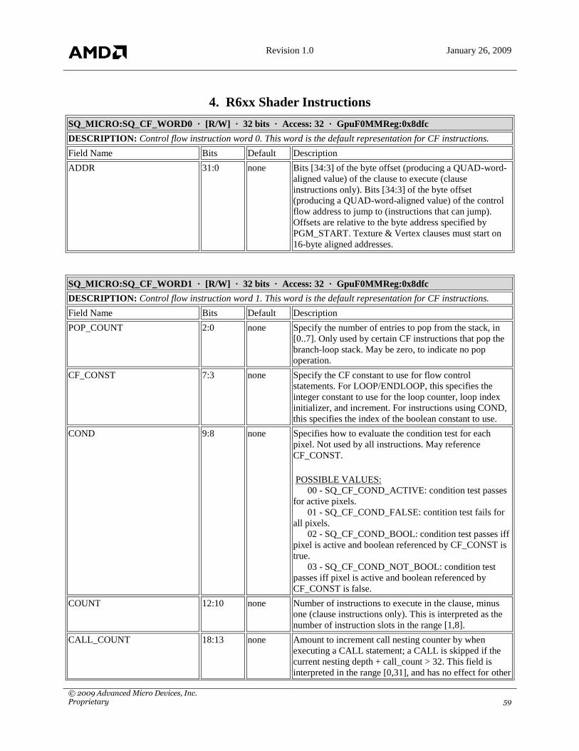
Revision 1.0 January 26, 2009
© 2009 Advanced Micro Devices, Inc. Proprietary 59
4. R6xx Shader Instructions
SQ_MICRO:SQ_CF_WORD0 · [R/W] · 32 bits · Access: 32 · GpuF0MMReg:0x8dfc
DESCRIPTION: Control flow instruction word 0. This word is the default representation for CF instructions.
Field Name Bits Default Description
ADDR 31:0 none Bits [34:3] of the byte offset (producing a QUAD-word-
aligned value) of the clause to execute (clause
instructions only). Bits [34:3] of the byte offset
(producing a QUAD-word-aligned value) of the control
flow address to jump to (instructions that can jump).
Offsets are relative to the byte address specified by
PGM_START. Texture & Vertex clauses must start on
16-byte aligned addresses.
SQ_MICRO:SQ_CF_WORD1 · [R/W] · 32 bits · Access: 32 · GpuF0MMReg:0x8dfc
DESCRIPTION: Control flow instruction word 1. This word is the default representation for CF instructions.
Field Name Bits Default Description
POP_COUNT 2:0 none Specify the number of entries to pop from the stack, in
[0..7]. Only used by certain CF instructions that pop the
branch-loop stack. May be zero, to indicate no pop
operation.
CF_CONST 7:3 none Specify the CF constant to use for flow control
statements. For LOOP/ENDLOOP, this specifies the
integer constant to use for the loop counter, loop index
initializer, and increment. For instructions using COND,
this specifies the index of the boolean constant to use.
COND 9:8 none Specifies how to evaluate the condition test for each
pixel. Not used by all instructions. May reference
CF_CONST.
POSSIBLE VALUES:
00 - SQ_CF_COND_ACTIVE: condition test passes
for active pixels.
01 - SQ_CF_COND_FALSE: contition test fails for
all pixels.
02 - SQ_CF_COND_BOOL: condition test passes iff
pixel is active and boolean referenced by CF_CONST is
true.
03 - SQ_CF_COND_NOT_BOOL: condition test
passes iff pixel is active and boolean referenced by
CF_CONST is false.
COUNT 12:10 none Number of instructions to execute in the clause, minus
one (clause instructions only). This is interpreted as the
number of instruction slots in the range [1,8].
CALL_COUNT 18:13 none Amount to increment call nesting counter by when
executing a CALL statement; a CALL is skipped if the
current nesting depth + call_count > 32. This field is
interpreted in the range [0,31], and has no effect for other

Revision 1.0 January 26, 2009
© 2009 Advanced Micro Devices, Inc. Proprietary 60
instruction types.
END_OF_PROGRAM 21 none If set, then this instruction is the last instruction of the
CF program. Execution ends after this instruction is
issued.
VALID_PIXEL_MODE 22 none If set, execute this instruction/clause as if invalid pixels
are inactive. Antonym of WHOLE_QUAD_MODE.
Caution: VALID_PIXEL_MODE is not the `default`
mode; this bit should be set to 0 by default.
CF_INST 29:23 none Type of instruction to evaluate in CF. For this encoding,
CF_INST must be set to one of the following values.
POSSIBLE VALUES:
00 - SQ_CF_INST_NOP: perform no operation.
01 - SQ_CF_INST_TEX: execute texture fetch or
constant fetch clause. CF_COND=ACTIVE is required.
02 - SQ_CF_INST_VTX: execute vertex fetch
clause. CF_COND=ACTIVE is required.
03 - SQ_CF_INST_VTX_TC: execute vertex fetch
clause through the texture cache (for systems lacking
VC). CF_COND=ACTIVE is required.
04 - SQ_CF_INST_LOOP_START: execute DX9
loop start instruction (push onto loop stack if loop body
executes).
05 - SQ_CF_INST_LOOP_END: execute DX9 loop
end instruction (pop loop stack if loop is finished).
06 - SQ_CF_INST_LOOP_START_DX10: execute
DX10 loop start instruction (push onto loop stack if loop
body executes).
07 - SQ_CF_INST_LOOP_START_NO_AL: same
as LOOP_START but don`t push AL onto stack or
update AL.
08 - SQ_CF_INST_LOOP_CONTINUE: execute
continue statement (jump to end of loop if all pixels
ready to continue).
09 - SQ_CF_INST_LOOP_BREAK: execute a break
statement (pop loop stack if all pixels ready to break).
10 - SQ_CF_INST_JUMP: execute jump statement
(may be conditional).
11 - SQ_CF_INST_PUSH: push current per-pixel
active state onto stack OR jump and pop if no items
would be active.
12 - SQ_CF_INST_PUSH_ELSE: push current per-
pixel active state onto stack ND jump if no items would
be active.
13 - SQ_CF_INST_ELSE: execute else statement
(may be conditional) OR jump if no items would be
active.
14 - SQ_CF_INST_POP: pop current per-pixel state
from the stack. jump if no pixels were enabled prior to
pop.
15 - SQ_CF_INST_POP_JUMP: pop current per-
pixel state from the stack. then execute CF_INST_JUMP

Revision 1.0 January 26, 2009
© 2009 Advanced Micro Devices, Inc. Proprietary 61
with pop count = 0.
16 - SQ_CF_INST_POP_PUSH: pop current per-
pixel state from the stack. then execute CF_INST_PUSH
with pop count = 0.
17 - SQ_CF_INST_POP_PUSH_ELSE: pop current
per-pixel state from the stack. then execute
CF_INST_PUSH_ELSE.
18 - SQ_CF_INST_CALL: execute subroutine call
instruction (push onto address stack).
19 - SQ_CF_INST_CALL_FS: call fetch shader. The
address to call is stored in a state register in SQ.
20 - SQ_CF_INST_RETURN: execute subroutine
return instruction (pop address stack). Pair with
CF_INST_CALL only.
21 - SQ_CF_INST_EMIT_VERTEX: signal that GS
has finished exporting a vertex to memory.
CF_COND=ACTIVE is required.
22 - SQ_CF_INST_EMIT_CUT_VERTEX: emit a
vertex and an end of primitive strip marker. The next
emitted vertex will start a new primitive strip.
CF_COND=ACTIVE is required.
23 - SQ_CF_INST_CUT_VERTEX: emit an end of
primitive strip marker. The next emitted vertex will start
a new primitive strip. CF_COND=ACTIVE is required.
24 - SQ_CF_INST_KILL: kill pixels that pass the
condition test (may be conditional). jump if all pixels are
killed. CF_COND=ACTIVE is required.
WHOLE_QUAD_MODE 30 none If set, execute this instruction/clause as if all pixels are
active and valid. Antonym of VALID_PIXEL_MODE.
Set at most one of these bits.
BARRIER 31 none If set, all prior CF instructions/clauses must complete
before this instruction/clause executes. If not set, this
instruction/clause may run in parallel with prior
instructions.
SQ_MICRO:SQ_CF_ALU_WORD0 · [R/W] · 32 bits · Access: 32 · GpuF0MMReg:0x8dfc
DESCRIPTION: Control flow instruction word 0. This word is used by ALU clause instructions.
Field Name Bits Default Description
ADDR 21:0 none Bits [24:3] of the byte offset (producing a QUAD-word-
aligned value) of the clause to execute. The offset is
relative to the byte address specified by PGM_START.
KCACHE_BANK0 25:22 none Bank (constant buffer number) for first set of locked
cache lines.
KCACHE_BANK1 29:26 none Bank (constant buffer number) for second set of locked
cache lines.
KCACHE_MODE0 31:30 none Mode for first set of locked cache lines.
POSSIBLE VALUES:
00 - SQ_CF_KCACHE_NOP: do not lock any cache

Revision 1.0 January 26, 2009
© 2009 Advanced Micro Devices, Inc. Proprietary 62
lines.
01 - SQ_CF_KCACHE_LOCK_1: lock cache line
[bank][addr].
02 - SQ_CF_KCACHE_LOCK_2: lock cache lines
[bank][addr] and [bank][addr+1].
03 - SQ_CF_KCACHE_LOCK_LOOP_INDEX:
lock cache lines [bank][loop/16+addr] and
[bank][loop/16+addr+1], where loop is current loop
index.
SQ_MICRO:SQ_CF_ALU_WORD1 · [R/W] · 32 bits · Access: 32 · GpuF0MMReg:0x8dfc
DESCRIPTION: Control flow instruction word 1. This word is used by ALU clause instructions.
Field Name Bits Default Description
KCACHE_MODE1 1:0 none Mode for second set of locked cache lines.
POSSIBLE VALUES:
00 - SQ_CF_KCACHE_NOP: do not lock any cache
lines.
01 - SQ_CF_KCACHE_LOCK_1: lock cache line
[bank][addr].
02 - SQ_CF_KCACHE_LOCK_2: lock cache lines
[bank][addr] and [bank][addr+1].
03 - SQ_CF_KCACHE_LOCK_LOOP_INDEX:
lock cache lines [bank][loop/16+addr] and
[bank][loop/16+addr+1], where loop is current loop
index.
KCACHE_ADDR0 9:2 none Constant buffer address for first set of locked cache lines.
In units of cache lines where a line holds 16 128-bit
constants (byte addr[15:8]).
KCACHE_ADDR1 17:10 none Constant buffer address for second set of locked cache
lines.
COUNT 24:18 none Number of instructions to execute in the clause, minus
one. This is interpreted as the number of instruction slots
(64-bit slots) in the range [1,128].
USES_WATERFALL 25 none If set, then this ALU clause uses waterfall constants
(GPR-based indexing).
CF_INST 29:26 none Type of ALU instruction to evaluate in CF. For this
encoding, CF_INST must be set to one of the following
values.
POSSIBLE VALUES:
08 - SQ_CF_INST_ALU: each PRED_SET updates
the active state but does not update the stack.
09 - SQ_CF_INST_ALU_PUSH_BEFORE: do
CF_PUSH; then CF_INST_ALU
10 - SQ_CF_INST_ALU_POP_AFTER: do
CF_INST_ALU; then do CF_INST_POP.
11 - SQ_CF_INST_ALU_POP2_AFTER: do

Revision 1.0 January 26, 2009
© 2009 Advanced Micro Devices, Inc. Proprietary 63
CF_INST_ALU; then do CF_INST_POP twice.
13 - SQ_CF_INST_ALU_CONTINUE: each
PRED_SET causes a continue operation on the masked
pixels. Equivalent to CF_INST_PUSH; CF_INST_ALU;
CF_INST_ELSE; CF_INST_CONTINUE; CF_POP.
14 - SQ_CF_INST_ALU_BREAK: each PRED_SET
causes a break operation on the masked pixels.
Equivalent to CF_INST_PUSH; CF_INST_ALU;
CF_INST_ELSE; CF_INST_CONTINUE; CF_POP.
15 - SQ_CF_INST_ALU_ELSE_AFTER: do
CF_INST_ALU; then do CF_INST_ELSE.
WHOLE_QUAD_MODE 30 none If set, execute this instruction/clause as if all pixels are
active and valid. Antonym of VALID_PIXEL_MODE.
Set at most one of these bits.
BARRIER 31 none If set, all prior CF instructions/clauses must complete
before this instruction/clause executes. If not set, this
instruction/clause may run in parallel with prior
instructions.
SQ_MICRO:SQ_CF_ALLOC_EXPORT_WORD0 · [R/W] · 32 bits · Access: 32 · GpuF0MMReg:0x8dfc
DESCRIPTION: Word 0 of the control flow instruction for alloc/export.
Field Name Bits Default Description
ARRAY_BASE 12:0 none For scratch/reduction input/output, this is the base
address of the array in multiples of 4 dwords [0,32764].
For stream/ring output, this is the base addess of the
array in multiples of 1 dword [0,8191].
For pixel/z output, this is the index of the first export
(framebuffer, no fog: 0..7; framebuffer, with fog: 16..23;
computed Z: 61).
For parameter output, this is the parameter index of the
first export [0,31].
For position output, this is the position index of the first
export [60,63].
TYPE 14:13 none Type of allocation/export. In the table below, the first
enumeration value listed (PIXEL, POS, PARAM) is used
with CF_INST_EXPORT*. The second enumeration
value listed (WRITE, WRITE_IND, READ, and
READ_IND) is used with CF_INST_MEM*.
POSSIBLE VALUES:
00 - SQ_EXPORT_PIXEL: write pixel.
SQ_EXPORT_WRITE: write to memory buffer.
01 - SQ_EXPORT_POS: write position.
SQ_EXPORT_WRITE_IND: write to memory buffer,
use offset in INDEX_GPR.

Revision 1.0 January 26, 2009
© 2009 Advanced Micro Devices, Inc. Proprietary 64
02 - SQ_EXPORT_PARAM: write parameter cache.
SQ_EXPORT_READ: read from memory buffer (scratch
and reduction only).
03 - Unused for SX exports.
SQ_EXPORT_READ_IND: read from memory buffer,
use offset in INDEX_GPR (scratch and reduction only).
RW_GPR 21:15 none GPR register to read data from or write data to.
RW_REL 22 none Indicates whether GPR is an absolute address, or relative
to the loop index.
POSSIBLE VALUES:
00 - SQ_ABSOLUTE: no relative addressing.
01 - SQ_RELATIVE: add current loop index value to
this address.
INDEX_GPR 29:23 none For any indexed export, this GPR contains an index that
will be used in the computation for determining the
address of the first export. The index is multipled by
(ELEM_SIZE + 1). Only the X component is used (other
components ignored, no swizzle allowed).
ELEM_SIZE 31:30 none Number of DWORDs per element, minus one. This field
is interpreted as a value in [1,4]. The value from
INDEX_GPR and the loop counter are multiplied by this
factor, if applicable. Also, BURST_COUNT is
multiplied by this factor for CF_INST_MEM*. This field
is ignored for CF_INST_EXPORT*. Normally,
ELEMSIZE = 4 DWORDs for scratch & reduction, one
DWORD for other types.
SQ_MICRO:SQ_CF_ALLOC_EXPORT_WORD1 · [R/W] · 32 bits · Access: 32 · GpuF0MMReg:0x8dfc
DESCRIPTION: Word 1 of the control flow instruction for alloc/export is the bitwise OR of WORD1 |
WORD1_{BUF,SWIZ}. This part contains fields that are always defined.
Field Name Bits Default Description
BURST_COUNT 20:17 none Number of MRTs, positions, parameters, or logical
export values to allocate and/or export, minus one. This
field is interpreted as a value in [1,16].
END_OF_PROGRAM 21 none If set, then this instruction is the last instruction of the
CF program. Execution ends after this instruction is
issued.
VALID_PIXEL_MODE 22 none If set, execute this instruction/clause as if invalid pixels
are inactive. Antonym of WHOLE_QUAD_MODE.
Caution: VALID_PIXEL_MODE is not the `default`
mode; this bit should be set to 0 by default.
CF_INST 29:23 none Type of instruction to evaluate in CF. This value MUST
be one of the alloc/export instructions listed below.
POSSIBLE VALUES:
32 - SQ_CF_INST_MEM_STREAM0: perform a
memory operation on the stream buffer 0 (write-only).

Revision 1.0 January 26, 2009
© 2009 Advanced Micro Devices, Inc. Proprietary 65
33 - SQ_CF_INST_MEM_STREAM1: perform a
memory operation on the stream buffer 1 (write-only).
34 - SQ_CF_INST_MEM_STREAM2: perform a
memory operation on the stream buffer 2 (write-only).
35 - SQ_CF_INST_MEM_STREAM3: perform a
memory operation on the stream buffer 3 (write-only).
36 - SQ_CF_INST_MEM_SCRATCH: perform a
memory operation on the scratch buffer (read-write).
37 - SQ_CF_INST_MEM_REDUCTION: perform a
memory operation on the reduction buffer (read-write).
38 - SQ_CF_INST_MEM_RING: perform a memory
operation on the ring buffer (write-only).
39 - SQ_CF_INST_EXPORT: export only (not last).
Used for PIXEL, POS, PARAM exports.
40 - SQ_CF_INST_EXPORT_DONE: export only
(last export). Used for PIXEL, POS, PARAM exports.
WHOLE_QUAD_MODE 30 none If set, execute this instruction/clause as if all pixels were
active and valid.
BARRIER 31 none If set, all prior CF instructions/clauses must complete
before this instruction/clause executes. If not set, this
instruction/clause may run in parallel with prior
instructions.
SQ_MICRO:SQ_CF_ALLOC_EXPORT_WORD1_BUF · [R/W] · 32 bits · Access: 32 ·
GpuF0MMReg:0x8dfc
DESCRIPTION: Word 1 of the control flow instruction. This subencoding is used by alloc/exports for all
input/outputs to scratch/ring/stream/reduction buffers.
Field Name Bits Default Description
ARRAY_SIZE 11:0 none Array size (elem-size units). Represents values [1,4096]
when ELEMSIZE=0, [4,16384] when ELEMSIZE=3.
COMP_MASK 15:12 none XYZW component mask (X is the LSB). Write the
component iff the corresponding bit is 1. Applies only to
writes, not reads.
SQ_MICRO:SQ_CF_ALLOC_EXPORT_WORD1_SWIZ · [R/W] · 32 bits · Access: 32 ·
GpuF0MMReg:0x8dfc
DESCRIPTION: Word 1 of the control flow instruction. This subencoding is used by alloc/exports for PIXEL,
POS, and PARAM.
Field Name Bits Default Description
SEL_X 2:0 none Specify source for each component of the export.
POSSIBLE VALUES:
00 - SQ_SEL_X: use X component
01 - SQ_SEL_Y: use Y component
02 - SQ_SEL_Z: use Z component
03 - SQ_SEL_W: use W component
04 - SQ_SEL_0: use constant 0.0
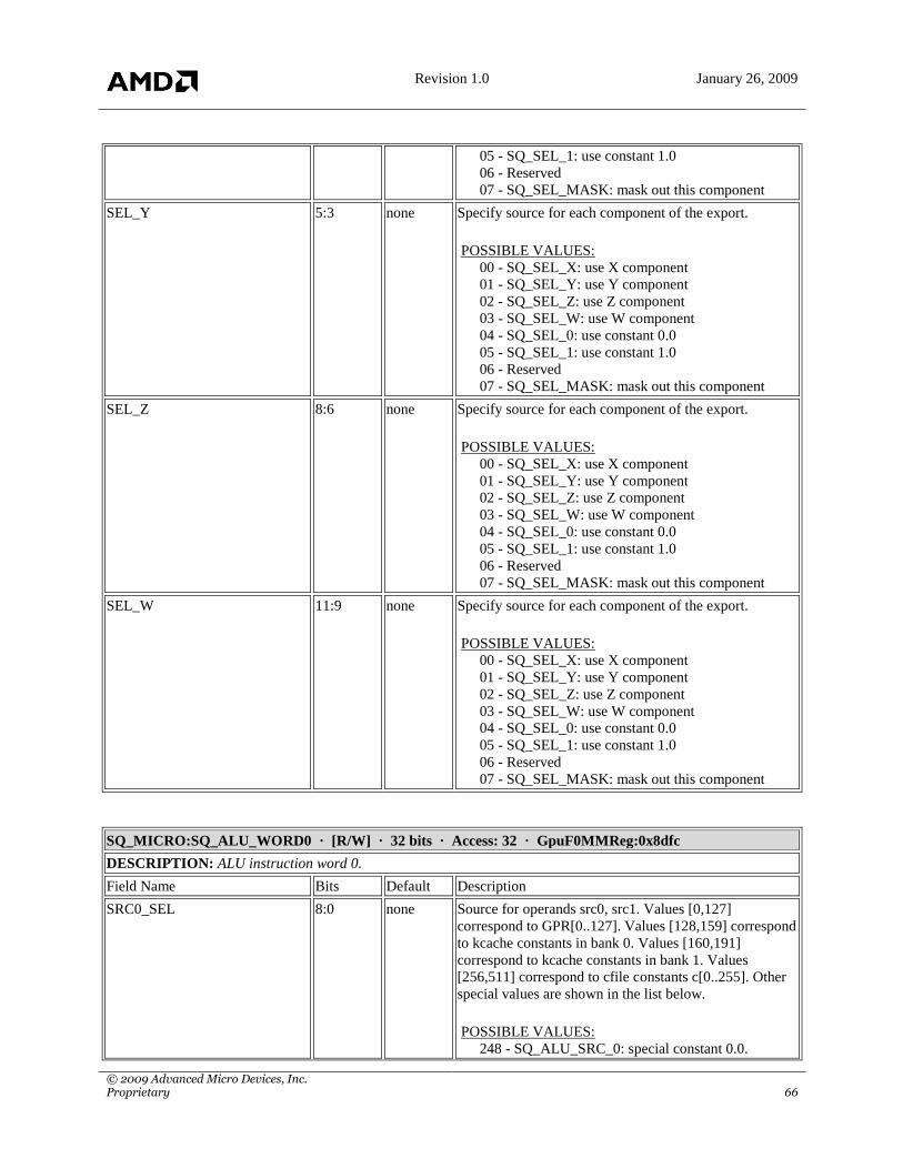
Revision 1.0 January 26, 2009
© 2009 Advanced Micro Devices, Inc. Proprietary 66
05 - SQ_SEL_1: use constant 1.0
06 - Reserved
07 - SQ_SEL_MASK: mask out this component
SEL_Y 5:3 none Specify source for each component of the export.
POSSIBLE VALUES:
00 - SQ_SEL_X: use X component
01 - SQ_SEL_Y: use Y component
02 - SQ_SEL_Z: use Z component
03 - SQ_SEL_W: use W component
04 - SQ_SEL_0: use constant 0.0
05 - SQ_SEL_1: use constant 1.0
06 - Reserved
07 - SQ_SEL_MASK: mask out this component
SEL_Z 8:6 none Specify source for each component of the export.
POSSIBLE VALUES:
00 - SQ_SEL_X: use X component
01 - SQ_SEL_Y: use Y component
02 - SQ_SEL_Z: use Z component
03 - SQ_SEL_W: use W component
04 - SQ_SEL_0: use constant 0.0
05 - SQ_SEL_1: use constant 1.0
06 - Reserved
07 - SQ_SEL_MASK: mask out this component
SEL_W 11:9 none Specify source for each component of the export.
POSSIBLE VALUES:
00 - SQ_SEL_X: use X component
01 - SQ_SEL_Y: use Y component
02 - SQ_SEL_Z: use Z component
03 - SQ_SEL_W: use W component
04 - SQ_SEL_0: use constant 0.0
05 - SQ_SEL_1: use constant 1.0
06 - Reserved
07 - SQ_SEL_MASK: mask out this component
SQ_MICRO:SQ_ALU_WORD0 · [R/W] · 32 bits · Access: 32 · GpuF0MMReg:0x8dfc
DESCRIPTION: ALU instruction word 0.
Field Name Bits Default Description
SRC0_SEL 8:0 none Source for operands src0, src1. Values [0,127]
correspond to GPR[0..127]. Values [128,159] correspond
to kcache constants in bank 0. Values [160,191]
correspond to kcache constants in bank 1. Values
[256,511] correspond to cfile constants c[0..255]. Other
special values are shown in the list below.
POSSIBLE VALUES:
248 - SQ_ALU_SRC_0: special constant 0.0.
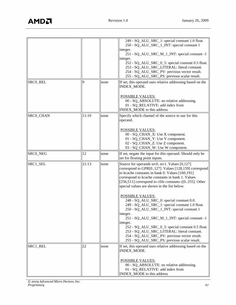
Revision 1.0 January 26, 2009
© 2009 Advanced Micro Devices, Inc. Proprietary 67
249 - SQ_ALU_SRC_1: special constant 1.0 float.
250 - SQ_ALU_SRC_1_INT: special constant 1
integer.
251 - SQ_ALU_SRC_M_1_INT: special constant -1
integer.
252 - SQ_ALU_SRC_0_5: special constant 0.5 float.
253 - SQ_ALU_SRC_LITERAL: literal constant.
254 - SQ_ALU_SRC_PV: previous vector result.
255 - SQ_ALU_SRC_PS: previous scalar result.
SRC0_REL 9 none If set, this operand uses relative addressing based on the
INDEX_MODE.
POSSIBLE VALUES:
00 - SQ_ABSOLUTE: no relative addressing.
01 - SQ_RELATIVE: add index from
INDEX_MODE to this address
SRC0_CHAN 11:10 none Specify which channel of the source to use for this
operand.
POSSIBLE VALUES:
00 - SQ_CHAN_X: Use X component.
01 - SQ_CHAN_Y: Use Y component.
02 - SQ_CHAN_Z: Use Z component.
03 - SQ_CHAN_W: Use W component.
SRC0_NEG 12 none If set, negate the input for this operand. Should only be
set for floating point inputs.
SRC1_SEL 21:13 none Source for operands src0, src1. Values [0,127]
correspond to GPR[0..127]. Values [128,159] correspond
to kcache constants in bank 0. Values [160,191]
correspond to kcache constants in bank 1. Values
[256,511] correspond to cfile constants c[0..255]. Other
special values are shown in the list below.
POSSIBLE VALUES:
248 - SQ_ALU_SRC_0: special constant 0.0.
249 - SQ_ALU_SRC_1: special constant 1.0 float.
250 - SQ_ALU_SRC_1_INT: special constant 1
integer.
251 - SQ_ALU_SRC_M_1_INT: special constant -1
integer.
252 - SQ_ALU_SRC_0_5: special constant 0.5 float.
253 - SQ_ALU_SRC_LITERAL: literal constant.
254 - SQ_ALU_SRC_PV: previous vector result.
255 - SQ_ALU_SRC_PS: previous scalar result.
SRC1_REL 22 none If set, this operand uses relative addressing based on the
INDEX_MODE.
POSSIBLE VALUES:
00 - SQ_ABSOLUTE: no relative addressing.
01 - SQ_RELATIVE: add index from
INDEX_MODE to this address

Revision 1.0 January 26, 2009
© 2009 Advanced Micro Devices, Inc. Proprietary 68
SRC1_CHAN 24:23 none Specify which channel of the source to use for this
operand.
POSSIBLE VALUES:
00 - SQ_CHAN_X: Use X component.
01 - SQ_CHAN_Y: Use Y component.
02 - SQ_CHAN_Z: Use Z component.
03 - SQ_CHAN_W: Use W component.
SRC1_NEG 25 none If set, negate the input for this operand. Should only be
set for floating point inputs.
INDEX_MODE 28:26 none Specify what relative addressing mode to use for
operands that have the REL bit set.
POSSIBLE VALUES:
00 - SQ_INDEX_AR_X: constants: add AR.X.
registers: add GPR index.
01 - SQ_INDEX_AR_Y: constants: add AR.Y.
registers: add GPR index.
02 - SQ_INDEX_AR_Z: constants: add AR.Z.
registers: add GPR index.
03 - SQ_INDEX_AR_W: constants: add AR.W.
registers: add GPR index.
04 - SQ_INDEX_LOOP: add current loop index
value.
PRED_SEL 30:29 none Predicate to apply to this instruction.
POSSIBLE VALUES:
00 - SQ_PRED_SEL_OFF: execute all pixels.
01 - Reserved
02 - SQ_PRED_SEL_ZERO: execute when pred = 0.
03 - SQ_PRED_SEL_ONE: execute when pred = 1.
LAST 31 none If set, this is the last 64-bit word for this instruction.
SQ_MICRO:SQ_ALU_WORD1 · [R/W] · 32 bits · Access: 32 · GpuF0MMReg:0x8dfc
DESCRIPTION: ALU instruction word 1 is the bitwise OR of SQ_ALU_WORD1 | SQ_ALU_WORD1_OP[2,3].
SQ_ALU_WORD1 contains fields used by all encodings.
Field Name Bits Default Description
ENCODING 17:15 none A read-only field used to determine whether OP2 or OP3
encoding is being used. If this field`s value is 0, the
instruction is using OP2. Otherwise, the instruction is
using OP3. Do not write to this field directly.
BANK_SWIZZLE 20:18 none Specify how to load operands into the SP.
POSSIBLE VALUES:
00 - SQ_ALU_VEC_012, SQ_ALU_SCL_210
01 - SQ_ALU_VEC_021, SQ_ALU_SCL_122
02 - SQ_ALU_VEC_120, SQ_ALU_SCL_212
03 - SQ_ALU_VEC_102, SQ_ALU_SCL_221
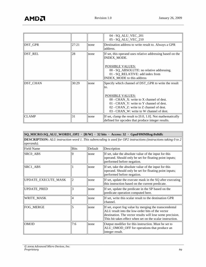
Revision 1.0 January 26, 2009
© 2009 Advanced Micro Devices, Inc. Proprietary 69
04 - SQ_ALU_VEC_201
05 - SQ_ALU_VEC_210
DST_GPR 27:21 none Destination address to write result to. Always a GPR
address.
DST_REL 28 none If set, this operand uses relative addressing based on the
INDEX_MODE.
POSSIBLE VALUES:
00 - SQ_ABSOLUTE: no relative addressing.
01 - SQ_RELATIVE: add index from
INDEX_MODE to this address
DST_CHAN 30:29 none Specify which channel of DST_GPR to write the result
to.
POSSIBLE VALUES:
00 - CHAN_X: write to X channel of dest.
01 - CHAN_Y: write to Y channel of dest.
02 - CHAN_Z: write to Z channel of dest.
03 - CHAN_W: write to W channel of dest.
CLAMP 31 none If set, clamp the result to [0.0, 1.0]. Not mathematically
defined for opcodes that produce integer results.
SQ_MICRO:SQ_ALU_WORD1_OP2 · [R/W] · 32 bits · Access: 32 · GpuF0MMReg:0x8dfc
DESCRIPTION: ALU instruction word 1. This subencoding is used for OP2 instructions (instructions taking 0 to 2
operands).
Field Name Bits Default Description
SRC0_ABS 0 none If set, take the absolute value of the input for this
operand. Should only be set for floating point inputs;
performed before negation.
SRC1_ABS 1 none If set, take the absolute value of the input for this
operand. Should only be set for floating point inputs;
performed before negation.
UPDATE_EXECUTE_MASK 2 none If set, update the execute mask in the SQ after executing
this instruction based on the current predicate.
UPDATE_PRED 3 none If set, update the predicate in the SP based on the
predicate operation computed here.
WRITE_MASK 4 none If set, write this scalar result to the destination GPR
channel.
FOG_MERGE 5 none If set, export fog value by merging the transcendental
ALU result into the low-order bits of the vector
destination. The vector results will lose some precision.
This bit takes effect when set on the scalar instruction.
OMOD 7:6 none Output modifier for this instruction. Must be set to
ALU_OMOD_OFF for operations that produce an
integer result.

Revision 1.0 January 26, 2009
© 2009 Advanced Micro Devices, Inc. Proprietary 70
POSSIBLE VALUES:
00 - SQ_ALU_OMOD_OFF: identity.
01 - SQ_ALU_OMOD_M2: multiply by 2.0.
02 - SQ_ALU_OMOD_M4: multiply by 4.0.
03 - SQ_ALU_OMOD_D2: divide by 2.0.
ALU_INST 17:8 none Instruction opcode. The top 3 bits of this must be zero.
Caution: gaps in opcode values are not marked in the
table below.
POSSIBLE VALUES:
00 - SQ_OP2_INST_ADD
01 - SQ_OP2_INST_MUL
02 - SQ_OP2_INST_MUL_IEEE
03 - SQ_OP2_INST_MAX
04 - SQ_OP2_INST_MIN
05 - SQ_OP2_INST_MAX_DX10
06 - SQ_OP2_INST_MIN_DX10
08 - SQ_OP2_INST_SETE
09 - SQ_OP2_INST_SETGT
10 - SQ_OP2_INST_SETGE
11 - SQ_OP2_INST_SETNE
12 - SQ_OP2_INST_SETE_DX10
13 - SQ_OP2_INST_SETGT_DX10
14 - SQ_OP2_INST_SETGE_DX10
15 - SQ_OP2_INST_SETNE_DX10
16 - SQ_OP2_INST_FRACT
17 - SQ_OP2_INST_TRUNC
18 - SQ_OP2_INST_CEIL
19 - SQ_OP2_INST_RNDNE
20 - SQ_OP2_INST_FLOOR
21 - SQ_OP2_INST_MOVA
22 - SQ_OP2_INST_MOVA_FLOOR
24 - SQ_OP2_INST_MOVA_INT
25 - SQ_OP2_INST_MOV
26 - SQ_OP2_INST_NOP
30 - SQ_OP2_INST_PRED_SETGT_UINT
31 - SQ_OP2_INST_PRED_SETGE_UINT
32 - SQ_OP2_INST_PRED_SETE
33 - SQ_OP2_INST_PRED_SETGT
34 - SQ_OP2_INST_PRED_SETGE
35 - SQ_OP2_INST_PRED_SETNE
36 - SQ_OP2_INST_PRED_SET_INV
37 - SQ_OP2_INST_PRED_SET_POP
38 - SQ_OP2_INST_PRED_SET_CLR
39 - SQ_OP2_INST_PRED_SET_RESTORE
40 - SQ_OP2_INST_PRED_SETE_PUSH
41 - SQ_OP2_INST_PRED_SETGT_PUSH
42 - SQ_OP2_INST_PRED_SETGE_PUSH
43 - SQ_OP2_INST_PRED_SETNE_PUSH
44 - SQ_OP2_INST_KILLE
45 - SQ_OP2_INST_KILLGT

Revision 1.0 January 26, 2009
© 2009 Advanced Micro Devices, Inc. Proprietary 71
46 - SQ_OP2_INST_KILLGE
47 - SQ_OP2_INST_KILLNE
48 - SQ_OP2_INST_AND_INT
49 - SQ_OP2_INST_OR_INT
50 - SQ_OP2_INST_XOR_INT
51 - SQ_OP2_INST_NOT_INT
52 - SQ_OP2_INST_ADD_INT
53 - SQ_OP2_INST_SUB_INT
54 - SQ_OP2_INST_MAX_INT
55 - SQ_OP2_INST_MIN_INT
56 - SQ_OP2_INST_MAX_UINT
57 - SQ_OP2_INST_MIN_UINT
58 - SQ_OP2_INST_SETE_INT
59 - SQ_OP2_INST_SETGT_INT
60 - SQ_OP2_INST_SETGE_INT
61 - SQ_OP2_INST_SETNE_INT
62 - SQ_OP2_INST_SETGT_UINT
63 - SQ_OP2_INST_SETGE_UINT
64 - SQ_OP2_INST_KILLGT_UINT
65 - SQ_OP2_INST_KILLGE_UINT
66 - SQ_OP2_INST_PRED_SETE_INT
67 - SQ_OP2_INST_PRED_SETGT_INT
68 - SQ_OP2_INST_PRED_SETGE_INT
69 - SQ_OP2_INST_PRED_SETNE_INT
70 - SQ_OP2_INST_KILLE_INT
71 - SQ_OP2_INST_KILLGT_INT
72 - SQ_OP2_INST_KILLGE_INT
73 - SQ_OP2_INST_KILLNE_INT
74 - SQ_OP2_INST_PRED_SETE_PUSH_INT
75 - SQ_OP2_INST_PRED_SETGT_PUSH_INT
76 - SQ_OP2_INST_PRED_SETGE_PUSH_INT
77 - SQ_OP2_INST_PRED_SETNE_PUSH_INT
78 - SQ_OP2_INST_PRED_SETLT_PUSH_INT
79 - SQ_OP2_INST_PRED_SETLE_PUSH_INT
80 - SQ_OP2_INST_DOT4
81 - SQ_OP2_INST_DOT4_IEEE
82 - SQ_OP2_INST_CUBE
83 - SQ_OP2_INST_MAX4
96 - SQ_OP2_INST_MOVA_GPR_INT
97 - SQ_OP2_INST_EXP_IEEE
98 - SQ_OP2_INST_LOG_CLAMPED
99 - SQ_OP2_INST_LOG_IEEE
100 - SQ_OP2_INST_RECIP_CLAMPED
101 - SQ_OP2_INST_RECIP_FF
102 - SQ_OP2_INST_RECIP_IEEE
103 - SQ_OP2_INST_RECIPSQRT_CLAMPED
104 - SQ_OP2_INST_RECIPSQRT_FF
105 - SQ_OP2_INST_RECIPSQRT_IEEE
106 - SQ_OP2_INST_SQRT_IEEE
107 - SQ_OP2_INST_FLT_TO_INT
108 - SQ_OP2_INST_INT_TO_FLT
109 - SQ_OP2_INST_UINT_TO_FLT
110 - SQ_OP2_INST_SIN

Revision 1.0 January 26, 2009
© 2009 Advanced Micro Devices, Inc. Proprietary 72
111 - SQ_OP2_INST_COS
112 - SQ_OP2_INST_ASHR_INT
113 - SQ_OP2_INST_LSHR_INT
114 - SQ_OP2_INST_LSHL_INT
115 - SQ_OP2_INST_MULLO_INT
116 - SQ_OP2_INST_MULHI_INT
117 - SQ_OP2_INST_MULLO_UINT
118 - SQ_OP2_INST_MULHI_UINT
119 - SQ_OP2_INST_RECIP_INT
120 - SQ_OP2_INST_RECIP_UINT
121 - SQ_OP2_INST_FLT_TO_UINT
SQ_MICRO:SQ_ALU_WORD1_OP3 · [R/W] · 32 bits · Access: 32 · GpuF0MMReg:0x8dfc
DESCRIPTION: ALU instruction word 1. This subencoding is used for OP3 instructions (instructions taking 3
operands).
Field Name Bits Default Description
SRC2_SEL 8:0 none Source for operands src2. Values [0,127] correspond to
GPR[0..127]. Values [128,159] correspond to kcache
constants in bank 0. Values [160,191] correspond to
kcache constants in bank 1. Values [256,511] correspond
to cfile constants c[0..255]. Other special values are
shown in the list below.
POSSIBLE VALUES:
248 - SQ_ALU_SRC_0: special constant 0.0.
249 - SQ_ALU_SRC_1: special constant 1.0 float.
250 - SQ_ALU_SRC_1_INT: special constant 1
integer.
251 - SQ_ALU_SRC_M_1_INT: special constant -1
integer.
252 - SQ_ALU_SRC_0_5: special constant 0.5 float.
253 - SQ_ALU_SRC_LITERAL: literal constant.
254 - SQ_ALU_SRC_PV: previous vector result.
255 - SQ_ALU_SRC_PS: previous scalar result.
SRC2_REL 9 none If set, this operand uses relative addressing based on the
INDEX_MODE.
POSSIBLE VALUES:
00 - SQ_ABSOLUTE: no relative addressing.
01 - SQ_RELATIVE: add index from
INDEX_MODE to this address
SRC2_CHAN 11:10 none Specify which channel of the source to use for this
operand.
POSSIBLE VALUES:
00 - SQ_CHAN_X: Use X component.
01 - SQ_CHAN_Y: Use Y component.
02 - SQ_CHAN_Z: Use Z component.
03 - SQ_CHAN_W: Use W component.

Revision 1.0 January 26, 2009
© 2009 Advanced Micro Devices, Inc. Proprietary 73
SRC2_NEG 12 none If set, negate the input for this operand. Should only be
set for floating point inputs.
ALU_INST 17:13 none Instruction opcode. Caution: opcode values do not begin
at zero.
POSSIBLE VALUES:
12 - SQ_OP3_INST_MUL_LIT
13 - SQ_OP3_INST_MUL_LIT_M2
14 - SQ_OP3_INST_MUL_LIT_M4
15 - SQ_OP3_INST_MUL_LIT_D2
16 - SQ_OP3_INST_MULADD
17 - SQ_OP3_INST_MULADD_M2
18 - SQ_OP3_INST_MULADD_M4
19 - SQ_OP3_INST_MULADD_D2
20 - SQ_OP3_INST_MULADD_IEEE
21 - SQ_OP3_INST_MULADD_IEEE_M2
22 - SQ_OP3_INST_MULADD_IEEE_M4
23 - SQ_OP3_INST_MULADD_IEEE_D2
24 - SQ_OP3_INST_CNDE
25 - SQ_OP3_INST_CNDGT
26 - SQ_OP3_INST_CNDGE
27 - Reserved
28 - SQ_OP3_INST_CNDE_INT
29 - SQ_OP3_INST_CNDGT_INT
30 - SQ_OP3_INST_CNDGE_INT
31 - Reserved
SQ_MICRO:SQ_VTX_WORD0 · [R/W] · 32 bits · Access: 32 · GpuF0MMReg:0x8dfc
DESCRIPTION: Vertex fetch clause instruction word 0.
Field Name Bits Default Description
VTX_INST 4:0 none Opcode for this vertex fetch instruction.
POSSIBLE VALUES:
00 - SQ_VTX_INST_FETCH: vertex fetch (X =
uint32 index)
01 - SQ_VTX_INST_SEMANTIC: semantic vertex
fetch
FETCH_TYPE 6:5 none Specify which index offset to send to VC.
POSSIBLE VALUES:
00 - SQ_VTX_FETCH_VERTEX_DATA
01 - SQ_VTX_FETCH_INSTANCE_DATA
02 - SQ_VTX_FETCH_NO_INDEX_OFFSET
FETCH_WHOLE_QUAD 7 none If set, texture instruction must fetch data for all pixels
(result may be used as source coordinate of a dependent
read). If cleared, texture instruction can ignore invalid
pixels.
BUFFER_ID 15:8 none Constant ID to use for this vertex fetch (indicates the
buffer address, size, and format).

Revision 1.0 January 26, 2009
© 2009 Advanced Micro Devices, Inc. Proprietary 74
SRC_GPR 22:16 none Source GPR address to get fetch address from.
SRC_REL 23 none Indicate whether source address is absolute or relative to
an index.
POSSIBLE VALUES:
00 - SQ_ABSOLUTE: no relative addressing.
01 - SQ_RELATIVE: add current loop index value to
this address.
SRC_SEL_X 25:24 none Indicate which component of src to use for the fetch
address.
POSSIBLE VALUES:
00 - SQ_SEL_X: use X component
01 - SQ_SEL_Y: use Y component
02 - SQ_SEL_Z: use Z component
03 - SQ_SEL_W: use W component
MEGA_FETCH_COUNT 31:26 none For a mega-fetch, number of bytes to fetch at once. For
mini-fetch, number of bytes to fetch if SQ converts this
instruction into a mega-fetch. This value`s range is
[1,64].
SQ_MICRO:SQ_VTX_WORD1 · [R/W] · 32 bits · Access: 32 · GpuF0MMReg:0x8dfc
DESCRIPTION: Vertex fetch clause instruction word 1 is the bitwise OR of WORD1 | WORD1_{GPR,SEM}. This
part contains fields shared by both subencodings.
Field Name Bits Default Description
DST_SEL_X 11:9 none Indicate which component of the result to write to
dst.XYZW. Can be used to mask out components when
writing to destination GPR.
POSSIBLE VALUES:
00 - SQ_SEL_X: use X component
01 - SQ_SEL_Y: use Y component
02 - SQ_SEL_Z: use Z component
03 - SQ_SEL_W: use W component
04 - SQ_SEL_0: use constant 0.0
05 - SQ_SEL_1: use constant 1.0
06 - Reserved
07 - SQ_SEL_MASK: mask out this component
DST_SEL_Y 14:12 none Indicate which component of the result to write to
dst.XYZW. Can be used to mask out components when
writing to destination GPR.
POSSIBLE VALUES:
00 - SQ_SEL_X: use X component
01 - SQ_SEL_Y: use Y component
02 - SQ_SEL_Z: use Z component
03 - SQ_SEL_W: use W component
04 - SQ_SEL_0: use constant 0.0

Revision 1.0 January 26, 2009
© 2009 Advanced Micro Devices, Inc. Proprietary 75
05 - SQ_SEL_1: use constant 1.0
06 - Reserved
07 - SQ_SEL_MASK: mask out this component
DST_SEL_Z 17:15 none Indicate which component of the result to write to
dst.XYZW. Can be used to mask out components when
writing to destination GPR.
POSSIBLE VALUES:
00 - SQ_SEL_X: use X component
01 - SQ_SEL_Y: use Y component
02 - SQ_SEL_Z: use Z component
03 - SQ_SEL_W: use W component
04 - SQ_SEL_0: use constant 0.0
05 - SQ_SEL_1: use constant 1.0
06 - Reserved
07 - SQ_SEL_MASK: mask out this component
DST_SEL_W 20:18 none Indicate which component of the result to write to
dst.XYZW. Can be used to mask out components when
writing to destination GPR.
POSSIBLE VALUES:
00 - SQ_SEL_X: use X component
01 - SQ_SEL_Y: use Y component
02 - SQ_SEL_Z: use Z component
03 - SQ_SEL_W: use W component
04 - SQ_SEL_0: use constant 0.0
05 - SQ_SEL_1: use constant 1.0
06 - Reserved
07 - SQ_SEL_MASK: mask out this component
USE_CONST_FIELDS 21 none If set, use format given in the fetch constant instead of in
this instruction.
DATA_FORMAT 27:22 none Indicate vertex data format (ignored if
USE_CONST_FIELDS = 1).
NUM_FORMAT_ALL 29:28 none Format of returning data (N is the number of bits derived
from DATA_FORMAT and gamma) (ignored if
USE_CONST_FIELDS = 1).
POSSIBLE VALUES:
00 - SQ_NUM_FORMAT_NORM: repeating
fraction number (0.N) with range [0, 1] if unsigned, or [-
1, 1] if signed.
01 - SQ_NUM_FORMAT_INT: integer number
(N.0) with range [0, 2^N] if unsigned, or [-2^M, 2^M] if
signed (M = N - 1).
02 - SQ_NUM_FORMAT_SCALED: integer
number stored as a S23E8 floating-point representation
(1 == 0x3f800000).
FORMAT_COMP_ALL 30 none Indicate sign of source components (ignored if
USE_CONST_FIELDS = 1).
Revision 1.0 January 26, 2009
© 2009 Advanced Micro Devices, Inc. Proprietary 76
POSSIBLE VALUES:
00 - SQ_FORMAT_COMP_UNSIGNED
01 - SQ_FORMAT_COMP_SIGNED
SRF_MODE_ALL 31 none Mapping to use when converting from signed RF to float
(ignored if USE_CONST_FIELDS = 1).
POSSIBLE VALUES:
00 -
SQ_SRF_MODE_ZERO_CLAMP_MINUS_ONE:
representation with two -1 representations (one is slightly
past -1 but clamped).
01 - SQ_SRF_MODE_NO_ZERO: OpenGL format
lacking representation for 0.
SQ_MICRO:SQ_VTX_WORD1_GPR · [R/W] · 32 bits · Access: 32 · GpuF0MMReg:0x8dfc
DESCRIPTION: Vertex fetch clause instruction word 1. This subencoding is used by fetch instructions that specify
a destination GPR directly.
Field Name Bits Default Description
DST_GPR 6:0 none Destination GPR address to write result to.
DST_REL 7 none Indicate whether destination address is absolute or
relative to an index.
POSSIBLE VALUES:
00 - SQ_ABSOLUTE: no relative addressing.
01 - SQ_RELATIVE: add current loop index value to
this address.
SQ_MICRO:SQ_VTX_WORD1_SEM · [R/W] · 32 bits · Access: 32 · GpuF0MMReg:0x8dfc
DESCRIPTION: Vertex fetch clause instruction word 1. This subencoding is used by semantic fetch instructions
that specify the destination using a semantic table.
Field Name Bits Default Description
SEMANTIC_ID 7:0 none Specify the 8-bit semantic ID used to lookup the
destination GPR from the semantic table.
SQ_MICRO:SQ_VTX_WORD2 · [R/W] · 32 bits · Access: 32 · GpuF0MMReg:0x8dfc
DESCRIPTION: Vertex fetch clause instruction word 2.
Field Name Bits Default Description
OFFSET 15:0 none Offset to begin reading from. Byte-aligned.
ENDIAN_SWAP 17:16 none Endian control (ignored if USE_CONST_FIELDS = 1).
POSSIBLE VALUES:
00 - SQ_ENDIAN_NONE: no endian swap (XOR by

Revision 1.0 January 26, 2009
© 2009 Advanced Micro Devices, Inc. Proprietary 77
0)
01 - SQ_ENDIAN_8IN16: 8 bit swap in 16 bit word
(XOR by 1): AABBCCDD -> BBAADDCC
02 - SQ_ENDIAN_8IN32: 8 bit swap in 32 bit word
(XOR by 3): AABBCCDD -> DDCCBBAA
CONST_BUF_NO_STRIDE 18 none If set, force stride to zero for constant buffer fetches that
use absolute addresses.
MEGA_FETCH 19 none If set, this instruction is a mega-fetch. Otherwise it is a
mini-fetch.
SQ_MICRO:SQ_TEX_WORD0 · [R/W] · 32 bits · Access: 32 · GpuF0MMReg:0x8dfc
DESCRIPTION: Texture fetch clause instruction word 0.
Field Name Bits Default Description
TEX_INST 4:0 none Opcode for this texture instruction.
POSSIBLE VALUES:
00 - SQ_TEX_INST_VTX_FETCH: vertex fetch (X
= uint32 index)
01 - SQ_TEX_INST_VTX_SEMANTIC: semantic
vertex fetch
02 - Reserved
03 - SQ_TEX_INST_LD: fetch texel, XYZL are
uint32
04 - SQ_TEX_INST_GET_TEXTURE_RESINFO:
retrieve width, height, depth, number of mipmap levels
05 -
SQ_TEX_INST_GET_NUMBER_OF_SAMPLES:
retrieve width, height, depth, number of samples of an
MSAA surface
06 - SQ_TEX_INST_GET_LOD: X = computed
LOD for all pixels in quad
07 - SQ_TEX_INST_GET_GRADIENTS_H: slopes
relative to horizontal: X = dx/dh, Y = dy/dh, Z = dz/dh,
W = dw/dh
08 - SQ_TEX_INST_GET_GRADIENTS_V: slopes
relative to vertical: X = dx/dv, Y = dy/dv, Z = dz/dv, W
= dw/dv
09 - SQ_TEX_INST_GET_LERP: retrieve weights
used for bilinear fetch, X = horizontal lerp, Y = vertical
lerp, Z = volume slice lerp, W = mipmap lerp
10 - SQ_TEX_INST_RESERVED_10: Reserved
(was GetWeight: retrieve weights used for bilinear fetch,
X = TL weight, Y = TR weight, Z = BL weight, W = BR
weight)
11 - SQ_TEX_INST_SET_GRADIENTS_H: XYZ
set horizontal gradients
12 - SQ_TEX_INST_SET_GRADIENTS_V: XYZ
set vertical gradients
13 - SQ_TEX_INST_PASS: returns the address read
in memory

Revision 1.0 January 26, 2009
© 2009 Advanced Micro Devices, Inc. Proprietary 78
14 - Z set index for array of cubemaps
15 - Reserved
16 - SQ_TEX_INST_SAMPLE
17 - SQ_TEX_INST_SAMPLE_L
18 - SQ_TEX_INST_SAMPLE_LB
19 - SQ_TEX_INST_SAMPLE_LZ
20 - SQ_TEX_INST_SAMPLE_G
21 - SQ_TEX_INST_SAMPLE_G_L
22 - SQ_TEX_INST_SAMPLE_G_LB
23 - SQ_TEX_INST_SAMPLE_G_LZ
24 - SQ_TEX_INST_SAMPLE_C
25 - SQ_TEX_INST_SAMPLE_C_L
26 - SQ_TEX_INST_SAMPLE_C_LB
27 - SQ_TEX_INST_SAMPLE_C_LZ
28 - SQ_TEX_INST_SAMPLE_C_G
29 - SQ_TEX_INST_SAMPLE_C_G_L
30 - SQ_TEX_INST_SAMPLE_C_G_LB
31 - SQ_TEX_INST_SAMPLE_C_G_LZ
BC_FRAC_MODE 5 none If set, force black texture data and white border to
retrieve fraction of pixel that hits the border.
FETCH_WHOLE_QUAD 7 none If set, texture instruction must fetch data for all pixels
(result may be used as source coordinate of a dependent
read). If cleared, texture instruction can ignore invalid
pixels.
RESOURCE_ID 15:8 none Surface ID to read from (specifies the buffer address,
size, and format). 160 available for GS and PS; 176
shared across FS and VS.
SRC_GPR 22:16 none Source GPR address to get the texture lookup address
from.
SRC_REL 23 none Indicate whether source address is absolute or relative to
an index.
POSSIBLE VALUES:
00 - SQ_ABSOLUTE: no relative addressing.
01 - SQ_RELATIVE: add current loop index value to
this address.
SQ_MICRO:SQ_TEX_WORD1 · [R/W] · 32 bits · Access: 32 · GpuF0MMReg:0x8dfc
DESCRIPTION: Texture fetch clause instruction word 1.
Field Name Bits Default Description
DST_GPR 6:0 none Destination GPR address to write result to.
DST_REL 7 none Indicate whether destination address is absolute or
relative to an index.
POSSIBLE VALUES:
00 - SQ_ABSOLUTE: no relative addressing.
01 - SQ_RELATIVE: add current loop index value to
this address.
Revision 1.0 January 26, 2009
© 2009 Advanced Micro Devices, Inc. Proprietary 79
DST_SEL_X 11:9 none Indicate which component of the result to write to
dst.XYZW. Can be used to mask out components when
writing to destination GPR.
POSSIBLE VALUES:
00 - SQ_SEL_X: use X component
01 - SQ_SEL_Y: use Y component
02 - SQ_SEL_Z: use Z component
03 - SQ_SEL_W: use W component
04 - SQ_SEL_0: use constant 0.0
05 - SQ_SEL_1: use constant 1.0
06 - Reserved
07 - SQ_SEL_MASK: mask out this component
DST_SEL_Y 14:12 none Indicate which component of the result to write to
dst.XYZW. Can be used to mask out components when
writing to destination GPR.
POSSIBLE VALUES:
00 - SQ_SEL_X: use X component
01 - SQ_SEL_Y: use Y component
02 - SQ_SEL_Z: use Z component
03 - SQ_SEL_W: use W component
04 - SQ_SEL_0: use constant 0.0
05 - SQ_SEL_1: use constant 1.0
06 - Reserved
07 - SQ_SEL_MASK: mask out this component
DST_SEL_Z 17:15 none Indicate which component of the result to write to
dst.XYZW. Can be used to mask out components when
writing to destination GPR.
POSSIBLE VALUES:
00 - SQ_SEL_X: use X component
01 - SQ_SEL_Y: use Y component
02 - SQ_SEL_Z: use Z component
03 - SQ_SEL_W: use W component
04 - SQ_SEL_0: use constant 0.0
05 - SQ_SEL_1: use constant 1.0
06 - Reserved
07 - SQ_SEL_MASK: mask out this component
DST_SEL_W 20:18 none Indicate which component of the result to write to
dst.XYZW. Can be used to mask out components when
writing to destination GPR.
POSSIBLE VALUES:
00 - SQ_SEL_X: use X component
01 - SQ_SEL_Y: use Y component
02 - SQ_SEL_Z: use Z component
03 - SQ_SEL_W: use W component
04 - SQ_SEL_0: use constant 0.0
05 - SQ_SEL_1: use constant 1.0
06 - Reserved
Revision 1.0 January 26, 2009
© 2009 Advanced Micro Devices, Inc. Proprietary 80
07 - SQ_SEL_MASK: mask out this component
LOD_BIAS 27:21 none Constant LOD bias to add to the computed bias for this
lookup. Twos-complement S3.4 fixpoint value with
range [-4, 4).
COORD_TYPE_X 28 none Indicate the type of the src.XYZW component.
POSSIBLE VALUES:
00 - SQ_TEX_UNNORMALIZED: Component is in
[0, dim); repeat and mirror modes unavailable.
01 - SQ_TEX_NORMALIZED: Component is in [0,
1]; repeat and mirror modes available.
COORD_TYPE_Y 29 none Indicate the type of the src.XYZW component.
POSSIBLE VALUES:
00 - SQ_TEX_UNNORMALIZED: Component is in
[0, dim); repeat and mirror modes unavailable.
01 - SQ_TEX_NORMALIZED: Component is in [0,
1]; repeat and mirror modes available.
COORD_TYPE_Z 30 none Indicate the type of the src.XYZW component.
POSSIBLE VALUES:
00 - SQ_TEX_UNNORMALIZED: Component is in
[0, dim); repeat and mirror modes unavailable.
01 - SQ_TEX_NORMALIZED: Component is in [0,
1]; repeat and mirror modes available.
COORD_TYPE_W 31 none Indicate the type of the src.XYZW component.
POSSIBLE VALUES:
00 - SQ_TEX_UNNORMALIZED: Component is in
[0, dim); repeat and mirror modes unavailable.
01 - SQ_TEX_NORMALIZED: Component is in [0,
1]; repeat and mirror modes available.
SQ_MICRO:SQ_TEX_WORD2 · [R/W] · 32 bits · Access: 32 · GpuF0MMReg:0x8dfc
DESCRIPTION: Texture fetch clause instruction word 2.
Field Name Bits Default Description
OFFSET_X 4:0 none Value added to X component of texel address before
sampling (in texel space). S3.1 fixpoint value ranging
from [-8, 8).
OFFSET_Y 9:5 none Value added to Y component of texel address before
sampling (in texel space). S3.1 fixpoint value ranging
from [-8, 8).
OFFSET_Z 14:10 none Value added to Z component of texel address before
sampling (in texel space). S3.1 fixpoint value ranging
from [-8, 8).
SAMPLER_ID 19:15 none Sampler ID to use (specifies filter options, etc.). Value in
the range [0, 17].

Revision 1.0 January 26, 2009
© 2009 Advanced Micro Devices, Inc. Proprietary 81
SRC_SEL_X 22:20 none Indicate component source for src.XYZW.
POSSIBLE VALUES:
00 - SQ_SEL_X: use X component
01 - SQ_SEL_Y: use Y component
02 - SQ_SEL_Z: use Z component
03 - SQ_SEL_W: use W component
04 - SQ_SEL_0: use constant 0.0
05 - SQ_SEL_1: use constant 1.0
SRC_SEL_Y 25:23 none Indicate component source for src.XYZW.
POSSIBLE VALUES:
00 - SQ_SEL_X: use X component
01 - SQ_SEL_Y: use Y component
02 - SQ_SEL_Z: use Z component
03 - SQ_SEL_W: use W component
04 - SQ_SEL_0: use constant 0.0
05 - SQ_SEL_1: use constant 1.0
SRC_SEL_Z 28:26 none Indicate component source for src.XYZW.
POSSIBLE VALUES:
00 - SQ_SEL_X: use X component
01 - SQ_SEL_Y: use Y component
02 - SQ_SEL_Z: use Z component
03 - SQ_SEL_W: use W component
04 - SQ_SEL_0: use constant 0.0
05 - SQ_SEL_1: use constant 1.0
SRC_SEL_W 31:29 none Indicate component source for src.XYZW.
POSSIBLE VALUES:
00 - SQ_SEL_X: use X component
01 - SQ_SEL_Y: use Y component
02 - SQ_SEL_Z: use Z component
03 - SQ_SEL_W: use W component
04 - SQ_SEL_0: use constant 0.0
05 - SQ_SEL_1: use constant 1.0

Revision 1.0 January 26, 2009
© 2009 Advanced Micro Devices, Inc. Proprietary 82
5. R7xx Shader Instructions
SQ_MICRO:SQ_CF_WORD0 · [R/W] · 32 bits · Access: 32 · GpuF0MMReg:0x8dfc
DESCRIPTION: Control flow instruction word 0. This word is the default representation for CF instructions.
Field Name Bits Default Description
ADDR 31:0 none Bits [34:3] of the byte offset (producing a QUAD-word-
aligned value) of the clause to execute (clause
instructions only). Bits [34:3] of the byte offset
(producing a QUAD-word-aligned value) of the control
flow address to jump to (instructions that can jump).
Offsets are relative to the byte address specified by
PGM_START. Texture & Vertex clauses must start on
16-byte aligned addresses.
SQ_MICRO:SQ_CF_WORD1 · [R/W] · 32 bits · Access: 32 · GpuF0MMReg:0x8dfc
DESCRIPTION: Control flow instruction word 1. This word is the default representation for CF instructions.
Field Name Bits Default Description
POP_COUNT 2:0 none Specify the number of entries to pop from the stack, in
[0..7]. Only used by certain CF instructions that pop the
branch-loop stack. May be zero, to indicate no pop
operation.
CF_CONST 7:3 none Specify the CF constant to use for flow control
statements. For LOOP/ENDLOOP, this specifies the
integer constant to use for the loop counter, loop index
initializer, and increment. For instructions using COND,
this specifies the index of the boolean constant to use.
COND 9:8 none Specifies how to evaluate the condition test for each
pixel. Not used by all instructions. May reference
CF_CONST.
POSSIBLE VALUES:
00 - SQ_CF_COND_ACTIVE: condition test passes
for active pixels.
01 - SQ_CF_COND_FALSE: contition test fails for
all pixels.
02 - SQ_CF_COND_BOOL: condition test passes iff
pixel is active and boolean referenced by CF_CONST is
true.
03 - SQ_CF_COND_NOT_BOOL: condition test
passes iff pixel is active and boolean referenced by
CF_CONST is false.
COUNT 12:10 none Number of instructions to execute in the clause, minus
one (clause instructions only). This is interpreted as the
number of instruction slots in the range [1,16]. MSB of
count is COUNT_3 field.
CALL_COUNT 18:13 none Amount to increment call nesting counter by when
executing a CALL statement; a CALL is skipped if the
current nesting depth + call_count > 32. This field is

Revision 1.0 January 26, 2009
© 2009 Advanced Micro Devices, Inc. Proprietary 83
interpreted in the range [0,31], and has no effect for other
instruction types.
COUNT_3 19 none MSB of COUNT field.
END_OF_PROGRAM 21 none If set, then this instruction is the last instruction of the
CF program. Execution ends after this instruction is
issued.
VALID_PIXEL_MODE 22 none If set, execute this instruction/clause as if invalid pixels
are inactive. Antonym of WHOLE_QUAD_MODE.
Caution: VALID_PIXEL_MODE is not the `default`
mode; this bit should be set to 0 by default.
CF_INST 29:23 none Type of instruction to evaluate in CF. For this encoding,
CF_INST must be set to one of the following values.
POSSIBLE VALUES:
00 - SQ_CF_INST_NOP: perform no operation.
01 - SQ_CF_INST_TEX: execute texture fetch
clause, through the texture cache. CF_COND=ACTIVE
is required.
02 - SQ_CF_INST_VTX: execute vertex fetch
clause, through the vertex-cache (if exists).
CF_COND=ACTIVE is required.
03 - SQ_CF_INST_VTX_TC: execute vertex fetch
clause through the texture cache. CF_COND=ACTIVE
is required.
04 - SQ_CF_INST_LOOP_START: execute DX9
loop start instruction (push onto loop stack if loop body
executes).
05 - SQ_CF_INST_LOOP_END: execute DX9 loop
end instruction (pop loop stack if loop is finished).
06 - SQ_CF_INST_LOOP_START_DX10: execute
DX10 loop start instruction (push onto loop stack if loop
body executes).
07 - SQ_CF_INST_LOOP_START_NO_AL: same
as LOOP_START but don`t push AL onto stack or
update AL.
08 - SQ_CF_INST_LOOP_CONTINUE: execute
continue statement (jump to end of loop if all pixels
ready to continue).
09 - SQ_CF_INST_LOOP_BREAK: execute a break
statement (pop loop stack if all pixels ready to break).
10 - SQ_CF_INST_JUMP: execute jump statement
(may be conditional).
11 - SQ_CF_INST_PUSH: push current per-pixel
active state onto stack OR jump and pop if no items
would be active.
12 - SQ_CF_INST_PUSH_ELSE: push current per-
pixel active state onto stack ND jump if no items would
be active.
13 - SQ_CF_INST_ELSE: execute else statement
(may be conditional) OR jump if no items would be
active.
14 - SQ_CF_INST_POP: pop current per-pixel state

Revision 1.0 January 26, 2009
© 2009 Advanced Micro Devices, Inc. Proprietary 84
from the stack. jump if no pixels were enabled prior to
pop.
15 - SQ_CF_INST_POP_JUMP: pop current per-
pixel state from the stack. then execute CF_INST_JUMP
with pop count = 0.
16 - SQ_CF_INST_POP_PUSH: pop current per-
pixel state from the stack. then execute CF_INST_PUSH
with pop count = 0.
17 - SQ_CF_INST_POP_PUSH_ELSE: pop current
per-pixel state from the stack. then execute
CF_INST_PUSH_ELSE.
18 - SQ_CF_INST_CALL: execute subroutine call
instruction (push onto address stack).
19 - SQ_CF_INST_CALL_FS: call fetch shader. The
address to call is stored in a state register in SQ.
20 - SQ_CF_INST_RETURN: execute subroutine
return instruction (pop address stack). Pair with
CF_INST_CALL only.
21 - SQ_CF_INST_EMIT_VERTEX: signal that GS
has finished exporting a vertex to memory.
CF_COND=ACTIVE is required.
22 - SQ_CF_INST_EMIT_CUT_VERTEX: emit a
vertex and an end of primitive strip marker. The next
emitted vertex will start a new primitive strip.
CF_COND=ACTIVE is required.
23 - SQ_CF_INST_CUT_VERTEX: emit an end of
primitive strip marker. The next emitted vertex will start
a new primitive strip. CF_COND=ACTIVE is required.
24 - SQ_CF_INST_KILL: kill pixels that pass the
condition test (may be conditional). jump if all pixels are
killed. CF_COND=ACTIVE is required.
WHOLE_QUAD_MODE 30 none If set, execute this instruction/clause as if all pixels are
active and valid. Antonym of VALID_PIXEL_MODE.
Set at most one of these bits.
BARRIER 31 none If set, all prior CF instructions/clauses must complete
before this instruction/clause executes. If not set, this
instruction/clause may run in parallel with prior
instructions.
SQ_MICRO:SQ_CF_ALU_WORD0 · [R/W] · 32 bits · Access: 32 · GpuF0MMReg:0x8dfc
DESCRIPTION: Control flow instruction word 0. This word is used by ALU clause instructions.
Field Name Bits Default Description
ADDR 21:0 none Bits [24:3] of the byte offset (producing a QUAD-word-
aligned value) of the clause to execute. The offset is
relative to the byte address specified by PGM_START.
KCACHE_BANK0 25:22 none Bank (constant buffer number) for first set of locked
cache lines.
KCACHE_BANK1 29:26 none Bank (constant buffer number) for second set of locked
cache lines.
Revision 1.0 January 26, 2009
© 2009 Advanced Micro Devices, Inc. Proprietary 85
KCACHE_MODE0 31:30 none Mode for first set of locked cache lines.
POSSIBLE VALUES:
00 - SQ_CF_KCACHE_NOP: do not lock any cache
lines.
01 - SQ_CF_KCACHE_LOCK_1: lock cache line
[bank][addr].
02 - SQ_CF_KCACHE_LOCK_2: lock cache lines
[bank][addr] and [bank][addr+1].
03 - SQ_CF_KCACHE_LOCK_LOOP_INDEX:
lock cache lines [bank][loop/16+addr] and
[bank][loop/16+addr+1], where loop is current loop
index.
SQ_MICRO:SQ_CF_ALU_WORD1 · [R/W] · 32 bits · Access: 32 · GpuF0MMReg:0x8dfc
DESCRIPTION: Control flow instruction word 1. This word is used by ALU clause instructions.
Field Name Bits Default Description
KCACHE_MODE1 1:0 none Mode for second set of locked cache lines.
POSSIBLE VALUES:
00 - SQ_CF_KCACHE_NOP: do not lock any cache
lines.
01 - SQ_CF_KCACHE_LOCK_1: lock cache line
[bank][addr].
02 - SQ_CF_KCACHE_LOCK_2: lock cache lines
[bank][addr] and [bank][addr+1].
03 - SQ_CF_KCACHE_LOCK_LOOP_INDEX:
lock cache lines [bank][loop/16+addr] and
[bank][loop/16+addr+1], where loop is current loop
index.
KCACHE_ADDR0 9:2 none Constant buffer address for first set of locked cache lines.
In units of cache lines where a line holds 16 128-bit
constants (byte addr[15:8]).
KCACHE_ADDR1 17:10 none Constant buffer address for second set of locked cache
lines.
COUNT 24:18 none Number of instructions to execute in the clause, minus
one. This is interpreted as the number of instruction slots
(64-bit slots) in the range [1,128].
ALT_CONST 25 none if set, uses constants from alternate thread type: ps->vs,
vs->gs, gs->vs, es->gs (note that es and vs share
constants).
CF_INST 29:26 none Type of ALU instruction to evaluate in CF. For this
encoding, CF_INST must be set to one of the following
values.
POSSIBLE VALUES:
08 - SQ_CF_INST_ALU: each PRED_SET updates
the active state but does not update the stack.

Revision 1.0 January 26, 2009
© 2009 Advanced Micro Devices, Inc. Proprietary 86
09 - SQ_CF_INST_ALU_PUSH_BEFORE: do
CF_PUSH; then CF_INST_ALU
10 - SQ_CF_INST_ALU_POP_AFTER: do
CF_INST_ALU; then do CF_INST_POP.
11 - SQ_CF_INST_ALU_POP2_AFTER: do
CF_INST_ALU; then do CF_INST_POP twice.
13 - SQ_CF_INST_ALU_CONTINUE: each
PRED_SET causes a continue operation on the masked
pixels. Equivalent to CF_INST_PUSH; CF_INST_ALU;
CF_INST_ELSE; CF_INST_CONTINUE; CF_POP.
14 - SQ_CF_INST_ALU_BREAK: each PRED_SET
causes a break operation on the masked pixels.
Equivalent to CF_INST_PUSH; CF_INST_ALU;
CF_INST_ELSE; CF_INST_CONTINUE; CF_POP.
15 - SQ_CF_INST_ALU_ELSE_AFTER: do
CF_INST_ALU; then do CF_INST_ELSE.
WHOLE_QUAD_MODE 30 none If set, execute this instruction/clause as if all pixels are
active and valid. Antonym of VALID_PIXEL_MODE.
Set at most one of these bits.
BARRIER 31 none If set, all prior CF instructions/clauses must complete
before this instruction/clause executes. If not set, this
instruction/clause may run in parallel with prior
instructions.
SQ_MICRO:SQ_CF_ALLOC_EXPORT_WORD0 · [R/W] · 32 bits · Access: 32 · GpuF0MMReg:0x8dfc
DESCRIPTION: Word 0 of the control flow instruction for alloc/export.
Field Name Bits Default Description
ARRAY_BASE 12:0 none For scratch/reduction input/output, this is the base
address of the array in multiples of 4 dwords [0,32764].
For stream/ring output, this is the base addess of the
array in multiples of 1 dword [0,8191].
For pixel/z output, this is the index of the first export
(framebuffer 0..7; computed Z: 61).
For parameter output, this is the parameter index of the
first export [0,31].
For position output, this is the position index of the first
export [60,63].
TYPE 14:13 none Type of allocation/export. In the table below, the first
enumeration value listed (PIXEL, POS, PARAM) is used
with CF_INST_EXPORT*. The second enumeration
value listed (WRITE, WRITE_IND, WRITE_ACK,
WRITE_IND_ACK) is used with CF_INST_MEM*.
POSSIBLE VALUES:
00 - SQ_EXPORT_PIXEL: write pixel.

Revision 1.0 January 26, 2009
© 2009 Advanced Micro Devices, Inc. Proprietary 87
SQ_EXPORT_WRITE: write to memory buffer.
01 - SQ_EXPORT_POS: write position.
SQ_EXPORT_WRITE_IND: write to memory buffer,
use offset in INDEX_GPR.
02 - SQ_EXPORT_PARAM: write parameter cache.
SQ_EXPORT_WRITE_ACK: write to memory buffer,
request an ACK when write is committed to memory.
03 - Unused for SX exports.
SQ_EXPORT_WRITE_IND_ACK: write to memory
buffer with offset in INDEX_GPR, get an ACK when
done.
RW_GPR 21:15 none GPR register to write data to.
RW_REL 22 none Indicates whether GPR is an absolute address, or relative
to the loop index.
POSSIBLE VALUES:
00 - SQ_ABSOLUTE: no relative addressing.
01 - SQ_RELATIVE: add current loop index value to
this address.
INDEX_GPR 29:23 none For any indexed export, this GPR contains an index that
will be used in the computation for determining the
address of the first export. The index is multipled by
(ELEM_SIZE + 1). Only the X component is used (other
components ignored, no swizzle allowed).
ELEM_SIZE 31:30 none Number of DWORDs per element, minus one. This field
is interpreted as a value in [1,2,4] (3 not supported). The
value from INDEX_GPR and the loop counter are
multiplied by this factor, if applicable. Also,
BURST_COUNT is multiplied by this factor for
CF_INST_MEM*. This field is ignored for
CF_INST_EXPORT*. Normally, ELEMSIZE = 4
DWORDs for scratch & reduction, one DWORD for
other types.
SQ_MICRO:SQ_CF_ALLOC_EXPORT_WORD1 · [R/W] · 32 bits · Access: 32 · GpuF0MMReg:0x8dfc
DESCRIPTION: Word 1 of the control flow instruction for alloc/export is the bitwise OR of WORD1 |
WORD1_{BUF,SWIZ}. This part contains fields that are always defined.
Field Name Bits Default Description
BURST_COUNT 20:17 none Number of MRTs, positions, parameters, or logical
export values to allocate and/or export, minus one. This
field is interpreted as a value in [1,16].
END_OF_PROGRAM 21 none If set, then this instruction is the last instruction of the
CF program. Execution ends after this instruction is
issued.
VALID_PIXEL_MODE 22 none If set, execute this instruction/clause as if invalid pixels
are inactive. Antonym of WHOLE_QUAD_MODE.
Caution: VALID_PIXEL_MODE is not the `default`
mode; this bit should be set to 0 by default.

Revision 1.0 January 26, 2009
© 2009 Advanced Micro Devices, Inc. Proprietary 88
CF_INST 29:23 none Type of instruction to evaluate in CF. This value MUST
be one of the alloc/export instructions listed below.
POSSIBLE VALUES:
32 - SQ_CF_INST_MEM_STREAM0: perform a
memory operation on the stream buffer 0 (write-only).
33 - SQ_CF_INST_MEM_STREAM1: perform a
memory operation on the stream buffer 1 (write-only).
34 - SQ_CF_INST_MEM_STREAM2: perform a
memory operation on the stream buffer 2 (write-only).
35 - SQ_CF_INST_MEM_STREAM3: perform a
memory operation on the stream buffer 3 (write-only).
36 - SQ_CF_INST_MEM_SCRATCH: perform a
memory operation on the scratch buffer (read-write).
37 - SQ_CF_INST_MEM_REDUCTION: perform a
memory operation on the reduction buffer (read-write).
38 - SQ_CF_INST_MEM_RING: perform a memory
operation on the ring buffer (write-only).
39 - SQ_CF_INST_EXPORT: export only (not last).
Used for PIXEL, POS, PARAM exports.
40 - SQ_CF_INST_EXPORT_DONE: export only
(last export). Used for PIXEL, POS, PARAM exports.
WHOLE_QUAD_MODE 30 none If set, execute this instruction/clause as if all pixels were
active and valid.
BARRIER 31 none If set, all prior CF instructions/clauses must complete
before this instruction/clause executes. If not set, this
instruction/clause may run in parallel with prior
instructions.
SQ_MICRO:SQ_CF_ALLOC_EXPORT_WORD1_BUF · [R/W] · 32 bits · Access: 32 ·
GpuF0MMReg:0x8dfc
DESCRIPTION: Word 1 of the control flow instruction. This subencoding is used by alloc/exports for all
input/outputs to scratch/ring/stream/reduction buffers.
Field Name Bits Default Description
ARRAY_SIZE 11:0 none Array size (elem-size units). Represents values [1,4096]
when ELEMSIZE=0, [4,16384] when ELEMSIZE=3.
COMP_MASK 15:12 none XYZW component mask (X is the LSB). Write the
component iff the corresponding bit is 1.
SQ_MICRO:SQ_CF_ALLOC_EXPORT_WORD1_SWIZ · [R/W] · 32 bits · Access: 32 ·
GpuF0MMReg:0x8dfc
DESCRIPTION: Word 1 of the control flow instruction. This subencoding is used by alloc/exports for PIXEL,
POS, and PARAM.
Field Name Bits Default Description
SEL_X 2:0 none Specify source for each component of the export.

Revision 1.0 January 26, 2009
© 2009 Advanced Micro Devices, Inc. Proprietary 89
POSSIBLE VALUES:
00 - SQ_SEL_X: use X component
01 - SQ_SEL_Y: use Y component
02 - SQ_SEL_Z: use Z component
03 - SQ_SEL_W: use W component
04 - SQ_SEL_0: use constant 0.0
05 - SQ_SEL_1: use constant 1.0
06 - Reserved
07 - SQ_SEL_MASK: mask out this component
SEL_Y 5:3 none Specify source for each component of the export.
POSSIBLE VALUES:
00 - SQ_SEL_X: use X component
01 - SQ_SEL_Y: use Y component
02 - SQ_SEL_Z: use Z component
03 - SQ_SEL_W: use W component
04 - SQ_SEL_0: use constant 0.0
05 - SQ_SEL_1: use constant 1.0
06 - Reserved
07 - SQ_SEL_MASK: mask out this component
SEL_Z 8:6 none Specify source for each component of the export.
POSSIBLE VALUES:
00 - SQ_SEL_X: use X component
01 - SQ_SEL_Y: use Y component
02 - SQ_SEL_Z: use Z component
03 - SQ_SEL_W: use W component
04 - SQ_SEL_0: use constant 0.0
05 - SQ_SEL_1: use constant 1.0
06 - Reserved
07 - SQ_SEL_MASK: mask out this component
SEL_W 11:9 none Specify source for each component of the export.
POSSIBLE VALUES:
00 - SQ_SEL_X: use X component
01 - SQ_SEL_Y: use Y component
02 - SQ_SEL_Z: use Z component
03 - SQ_SEL_W: use W component
04 - SQ_SEL_0: use constant 0.0
05 - SQ_SEL_1: use constant 1.0
06 - Reserved
07 - SQ_SEL_MASK: mask out this component
SQ_MICRO:SQ_ALU_WORD0 · [R/W] · 32 bits · Access: 32 · GpuF0MMReg:0x8dfc
DESCRIPTION: ALU instruction word 0.
Field Name Bits Default Description
SRC0_SEL 8:0 none Source for operands src0, src1. Values [0,127]
correspond to GPR[0..127]. Values [128,159] correspond

Revision 1.0 January 26, 2009
© 2009 Advanced Micro Devices, Inc. Proprietary 90
to kcache constants in bank 0. Values [160,191]
correspond to kcache constants in bank 1. Values
[256,511] correspond to cfile constants c[0..255]. Other
special values are shown in the list below.
POSSIBLE VALUES:
248 - SQ_ALU_SRC_0: special constant 0.0.
249 - SQ_ALU_SRC_1: special constant 1.0 float.
250 - SQ_ALU_SRC_1_INT: special constant 1
integer.
251 - SQ_ALU_SRC_M_1_INT: special constant -1
integer.
252 - SQ_ALU_SRC_0_5: special constant 0.5 float.
253 - SQ_ALU_SRC_LITERAL: literal constant.
254 - SQ_ALU_SRC_PV: previous vector result.
255 - SQ_ALU_SRC_PS: previous scalar result.
SRC0_REL 9 none If set, this operand uses relative addressing based on the
INDEX_MODE.
POSSIBLE VALUES:
00 - SQ_ABSOLUTE: no relative addressing.
01 - SQ_RELATIVE: add index from
INDEX_MODE to this address
SRC0_CHAN 11:10 none Specify which channel of the source to use for this
operand.
POSSIBLE VALUES:
00 - SQ_CHAN_X: Use X component.
01 - SQ_CHAN_Y: Use Y component.
02 - SQ_CHAN_Z: Use Z component.
03 - SQ_CHAN_W: Use W component.
SRC0_NEG 12 none If set, negate the input for this operand. Should only be
set for floating point inputs.
SRC1_SEL 21:13 none Source for operands src0, src1. Values [0,127]
correspond to GPR[0..127]. Values [128,159] correspond
to kcache constants in bank 0. Values [160,191]
correspond to kcache constants in bank 1. Values
[256,511] correspond to cfile constants c[0..255]. Other
special values are shown in the list below.
POSSIBLE VALUES:
248 - SQ_ALU_SRC_0: special constant 0.0.
249 - SQ_ALU_SRC_1: special constant 1.0 float.
250 - SQ_ALU_SRC_1_INT: special constant 1
integer.
251 - SQ_ALU_SRC_M_1_INT: special constant -1
integer.
252 - SQ_ALU_SRC_0_5: special constant 0.5 float.
253 - SQ_ALU_SRC_LITERAL: literal constant.
254 - SQ_ALU_SRC_PV: previous vector result.
255 - SQ_ALU_SRC_PS: previous scalar result.

Revision 1.0 January 26, 2009
© 2009 Advanced Micro Devices, Inc. Proprietary 91
SRC1_REL 22 none If set, this operand uses relative addressing based on the
INDEX_MODE.
POSSIBLE VALUES:
00 - SQ_ABSOLUTE: no relative addressing.
01 - SQ_RELATIVE: add index from
INDEX_MODE to this address
SRC1_CHAN 24:23 none Specify which channel of the source to use for this
operand.
POSSIBLE VALUES:
00 - SQ_CHAN_X: Use X component.
01 - SQ_CHAN_Y: Use Y component.
02 - SQ_CHAN_Z: Use Z component.
03 - SQ_CHAN_W: Use W component.
SRC1_NEG 25 none If set, negate the input for this operand. Should only be
set for floating point inputs.
INDEX_MODE 28:26 none Specify what relative addressing mode to use for
operands that have the REL bit set.
POSSIBLE VALUES:
00 - SQ_INDEX_AR_X: constants: add AR.X.
registers: add GPR index.
01 - SQ_INDEX_AR_Y: constants: add AR.Y.
registers: add GPR index.
02 - SQ_INDEX_AR_Z: constants: add AR.Z.
registers: add GPR index.
03 - SQ_INDEX_AR_W: constants: add AR.W.
registers: add GPR index.
04 - SQ_INDEX_LOOP: add current loop index
value.
PRED_SEL 30:29 none Predicate to apply to this instruction.
POSSIBLE VALUES:
00 - SQ_PRED_SEL_OFF: execute all pixels.
01 - Reserved
02 - SQ_PRED_SEL_ZERO: execute when pred = 0.
03 - SQ_PRED_SEL_ONE: execute when pred = 1.
LAST 31 none If set, this is the last 64-bit word for this instruction.
SQ_MICRO:SQ_ALU_WORD1 · [R/W] · 32 bits · Access: 32 · GpuF0MMReg:0x8dfc
DESCRIPTION: ALU instruction word 1 is the bitwise OR of SQ_ALU_WORD1 | SQ_ALU_WORD1_OP[2,3].
SQ_ALU_WORD1 contains fields used by all encodings.
Field Name Bits Default Description
ENCODING 17:15 none A read-only field used to determine whether OP2 or OP3
encoding is being used. If this field`s value is 0, the
instruction is using OP2. Otherwise, the instruction is
using OP3. Do not write to this field directly.

Revision 1.0 January 26, 2009
© 2009 Advanced Micro Devices, Inc. Proprietary 92
BANK_SWIZZLE 20:18 none Specify how to load operands into the SP.
POSSIBLE VALUES:
00 - SQ_ALU_VEC_012, SQ_ALU_SCL_210
01 - SQ_ALU_VEC_021, SQ_ALU_SCL_122
02 - SQ_ALU_VEC_120, SQ_ALU_SCL_212
03 - SQ_ALU_VEC_102, SQ_ALU_SCL_221
04 - SQ_ALU_VEC_201
05 - SQ_ALU_VEC_210
DST_GPR 27:21 none Destination address to write result to. Always a GPR
address.
DST_REL 28 none If set, this operand uses relative addressing based on the
INDEX_MODE.
POSSIBLE VALUES:
00 - SQ_ABSOLUTE: no relative addressing.
01 - SQ_RELATIVE: add index from
INDEX_MODE to this address
DST_CHAN 30:29 none Specify which channel of DST_GPR to write the result
to.
POSSIBLE VALUES:
00 - CHAN_X: write to X channel of dest.
01 - CHAN_Y: write to Y channel of dest.
02 - CHAN_Z: write to Z channel of dest.
03 - CHAN_W: write to W channel of dest.
CLAMP 31 none If set, clamp the result to [0.0, 1.0]. Not mathematically
defined for opcodes that produce integer results.
SQ_MICRO:SQ_ALU_WORD1_OP2_V2 · [R/W] · 32 bits · Access: 32 · GpuF0MMReg:0x8dfc
DESCRIPTION: ALU instruction word 1. This subencoding is used for OP2 instructions (instructions taking 0 to 2
operands).
Field Name Bits Default Description
SRC0_ABS 0 none If set, take the absolute value of the input for this
operand. Should only be set for floating point inputs;
performed before negation.
SRC1_ABS 1 none If set, take the absolute value of the input for this
operand. Should only be set for floating point inputs;
performed before negation.
UPDATE_EXECUTE_MASK 2 none If set, update the execute mask in the SQ after executing
this instruction based on the current predicate.
UPDATE_PRED 3 none If set, update the predicate in the SP based on the
predicate operation computed here.
WRITE_MASK 4 none If set, write this scalar result to the destination GPR
channel.
OMOD 6:5 none Output modifier for this instruction. Must be set to
ALU_OMOD_OFF for operations that produce an
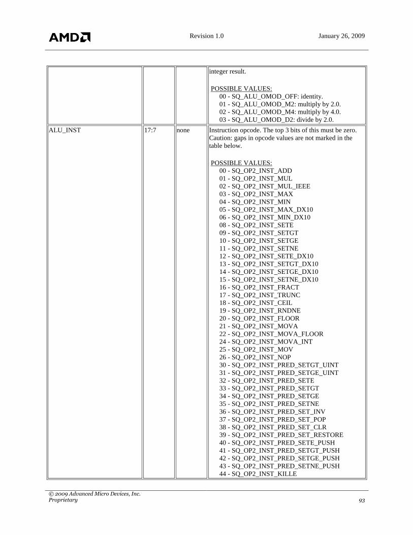
Revision 1.0 January 26, 2009
© 2009 Advanced Micro Devices, Inc. Proprietary 93
integer result.
POSSIBLE VALUES:
00 - SQ_ALU_OMOD_OFF: identity.
01 - SQ_ALU_OMOD_M2: multiply by 2.0.
02 - SQ_ALU_OMOD_M4: multiply by 4.0.
03 - SQ_ALU_OMOD_D2: divide by 2.0.
ALU_INST 17:7 none Instruction opcode. The top 3 bits of this must be zero.
Caution: gaps in opcode values are not marked in the
table below.
POSSIBLE VALUES:
00 - SQ_OP2_INST_ADD
01 - SQ_OP2_INST_MUL
02 - SQ_OP2_INST_MUL_IEEE
03 - SQ_OP2_INST_MAX
04 - SQ_OP2_INST_MIN
05 - SQ_OP2_INST_MAX_DX10
06 - SQ_OP2_INST_MIN_DX10
08 - SQ_OP2_INST_SETE
09 - SQ_OP2_INST_SETGT
10 - SQ_OP2_INST_SETGE
11 - SQ_OP2_INST_SETNE
12 - SQ_OP2_INST_SETE_DX10
13 - SQ_OP2_INST_SETGT_DX10
14 - SQ_OP2_INST_SETGE_DX10
15 - SQ_OP2_INST_SETNE_DX10
16 - SQ_OP2_INST_FRACT
17 - SQ_OP2_INST_TRUNC
18 - SQ_OP2_INST_CEIL
19 - SQ_OP2_INST_RNDNE
20 - SQ_OP2_INST_FLOOR
21 - SQ_OP2_INST_MOVA
22 - SQ_OP2_INST_MOVA_FLOOR
24 - SQ_OP2_INST_MOVA_INT
25 - SQ_OP2_INST_MOV
26 - SQ_OP2_INST_NOP
30 - SQ_OP2_INST_PRED_SETGT_UINT
31 - SQ_OP2_INST_PRED_SETGE_UINT
32 - SQ_OP2_INST_PRED_SETE
33 - SQ_OP2_INST_PRED_SETGT
34 - SQ_OP2_INST_PRED_SETGE
35 - SQ_OP2_INST_PRED_SETNE
36 - SQ_OP2_INST_PRED_SET_INV
37 - SQ_OP2_INST_PRED_SET_POP
38 - SQ_OP2_INST_PRED_SET_CLR
39 - SQ_OP2_INST_PRED_SET_RESTORE
40 - SQ_OP2_INST_PRED_SETE_PUSH
41 - SQ_OP2_INST_PRED_SETGT_PUSH
42 - SQ_OP2_INST_PRED_SETGE_PUSH
43 - SQ_OP2_INST_PRED_SETNE_PUSH
44 - SQ_OP2_INST_KILLE

Revision 1.0 January 26, 2009
© 2009 Advanced Micro Devices, Inc. Proprietary 94
45 - SQ_OP2_INST_KILLGT
46 - SQ_OP2_INST_KILLGE
47 - SQ_OP2_INST_KILLNE
48 - SQ_OP2_INST_AND_INT
49 - SQ_OP2_INST_OR_INT
50 - SQ_OP2_INST_XOR_INT
51 - SQ_OP2_INST_NOT_INT
52 - SQ_OP2_INST_ADD_INT
53 - SQ_OP2_INST_SUB_INT
54 - SQ_OP2_INST_MAX_INT
55 - SQ_OP2_INST_MIN_INT
56 - SQ_OP2_INST_MAX_UINT
57 - SQ_OP2_INST_MIN_UINT
58 - SQ_OP2_INST_SETE_INT
59 - SQ_OP2_INST_SETGT_INT
60 - SQ_OP2_INST_SETGE_INT
61 - SQ_OP2_INST_SETNE_INT
62 - SQ_OP2_INST_SETGT_UINT
63 - SQ_OP2_INST_SETGE_UINT
64 - SQ_OP2_INST_KILLGT_UINT
65 - SQ_OP2_INST_KILLGE_UINT
66 - SQ_OP2_INST_PRED_SETE_INT
67 - SQ_OP2_INST_PRED_SETGT_INT
68 - SQ_OP2_INST_PRED_SETGE_INT
69 - SQ_OP2_INST_PRED_SETNE_INT
70 - SQ_OP2_INST_KILLE_INT
71 - SQ_OP2_INST_KILLGT_INT
72 - SQ_OP2_INST_KILLGE_INT
73 - SQ_OP2_INST_KILLNE_INT
74 - SQ_OP2_INST_PRED_SETE_PUSH_INT
75 - SQ_OP2_INST_PRED_SETGT_PUSH_INT
76 - SQ_OP2_INST_PRED_SETGE_PUSH_INT
77 - SQ_OP2_INST_PRED_SETNE_PUSH_INT
78 - SQ_OP2_INST_PRED_SETLT_PUSH_INT
79 - SQ_OP2_INST_PRED_SETLE_PUSH_INT
80 - SQ_OP2_INST_DOT4
81 - SQ_OP2_INST_DOT4_IEEE
82 - SQ_OP2_INST_CUBE
83 - SQ_OP2_INST_MAX4
96 - SQ_OP2_INST_MOVA_GPR_INT
97 - SQ_OP2_INST_EXP_IEEE
98 - SQ_OP2_INST_LOG_CLAMPED
99 - SQ_OP2_INST_LOG_IEEE
100 - SQ_OP2_INST_RECIP_CLAMPED
101 - SQ_OP2_INST_RECIP_FF
102 - SQ_OP2_INST_RECIP_IEEE
103 - SQ_OP2_INST_RECIPSQRT_CLAMPED
104 - SQ_OP2_INST_RECIPSQRT_FF
105 - SQ_OP2_INST_RECIPSQRT_IEEE
106 - SQ_OP2_INST_SQRT_IEEE
107 - SQ_OP2_INST_FLT_TO_INT
108 - SQ_OP2_INST_INT_TO_FLT
109 - SQ_OP2_INST_UINT_TO_FLT

Revision 1.0 January 26, 2009
© 2009 Advanced Micro Devices, Inc. Proprietary 95
110 - SQ_OP2_INST_SIN
111 - SQ_OP2_INST_COS
112 - SQ_OP2_INST_ASHR_INT
113 - SQ_OP2_INST_LSHR_INT
114 - SQ_OP2_INST_LSHL_INT
115 - SQ_OP2_INST_MULLO_INT
116 - SQ_OP2_INST_MULHI_INT
117 - SQ_OP2_INST_MULLO_UINT
118 - SQ_OP2_INST_MULHI_UINT
119 - SQ_OP2_INST_RECIP_INT
120 - SQ_OP2_INST_RECIP_UINT
121 - SQ_OP2_INST_FLT_TO_UINT
SQ_MICRO:SQ_ALU_WORD1_OP3 · [R/W] · 32 bits · Access: 32 · GpuF0MMReg:0x8dfc
DESCRIPTION: ALU instruction word 1. This subencoding is used for OP3 instructions (instructions taking 3
operands).
Field Name Bits Default Description
SRC2_SEL 8:0 none Source for operands src2. Values [0,127] correspond to
GPR[0..127]. Values [128,159] correspond to kcache
constants in bank 0. Values [160,191] correspond to
kcache constants in bank 1. Values [256,511] correspond
to cfile constants c[0..255]. Other special values are
shown in the list below.
POSSIBLE VALUES:
248 - SQ_ALU_SRC_0: special constant 0.0.
249 - SQ_ALU_SRC_1: special constant 1.0 float.
250 - SQ_ALU_SRC_1_INT: special constant 1
integer.
251 - SQ_ALU_SRC_M_1_INT: special constant -1
integer.
252 - SQ_ALU_SRC_0_5: special constant 0.5 float.
253 - SQ_ALU_SRC_LITERAL: literal constant.
254 - SQ_ALU_SRC_PV: previous vector result.
255 - SQ_ALU_SRC_PS: previous scalar result.
SRC2_REL 9 none If set, this operand uses relative addressing based on the
INDEX_MODE.
POSSIBLE VALUES:
00 - SQ_ABSOLUTE: no relative addressing.
01 - SQ_RELATIVE: add index from
INDEX_MODE to this address
SRC2_CHAN 11:10 none Specify which channel of the source to use for this
operand.
POSSIBLE VALUES:
00 - SQ_CHAN_X: Use X component.
01 - SQ_CHAN_Y: Use Y component.
02 - SQ_CHAN_Z: Use Z component.

Revision 1.0 January 26, 2009
© 2009 Advanced Micro Devices, Inc. Proprietary 96
03 - SQ_CHAN_W: Use W component.
SRC2_NEG 12 none If set, negate the input for this operand. Should only be
set for floating point inputs.
ALU_INST 17:13 none Instruction opcode. Caution: opcode values do not begin
at zero.
POSSIBLE VALUES:
12 - SQ_OP3_INST_MUL_LIT
13 - SQ_OP3_INST_MUL_LIT_M2
14 - SQ_OP3_INST_MUL_LIT_M4
15 - SQ_OP3_INST_MUL_LIT_D2
16 - SQ_OP3_INST_MULADD
17 - SQ_OP3_INST_MULADD_M2
18 - SQ_OP3_INST_MULADD_M4
19 - SQ_OP3_INST_MULADD_D2
20 - SQ_OP3_INST_MULADD_IEEE
21 - SQ_OP3_INST_MULADD_IEEE_M2
22 - SQ_OP3_INST_MULADD_IEEE_M4
23 - SQ_OP3_INST_MULADD_IEEE_D2
24 - SQ_OP3_INST_CNDE
25 - SQ_OP3_INST_CNDGT
26 - SQ_OP3_INST_CNDGE
27 - Reserved
28 - SQ_OP3_INST_CNDE_INT
29 - SQ_OP3_INST_CNDGT_INT
30 - SQ_OP3_INST_CNDGE_INT
31 - Reserved
SQ_MICRO:SQ_VTX_WORD0 · [R/W] · 32 bits · Access: 32 · GpuF0MMReg:0x8dfc
DESCRIPTION: Vertex fetch clause instruction word 0.
Field Name Bits Default Description
VTX_INST 4:0 none Opcode for this vertex fetch instruction.
POSSIBLE VALUES:
00 - SQ_VTX_INST_FETCH: vertex fetch (X =
uint32 index)
01 - SQ_VTX_INST_SEMANTIC: semantic vertex
fetch
FETCH_TYPE 6:5 none Specify which index offset to send to VC.
POSSIBLE VALUES:
00 - SQ_VTX_FETCH_VERTEX_DATA
01 - SQ_VTX_FETCH_INSTANCE_DATA
02 - SQ_VTX_FETCH_NO_INDEX_OFFSET
FETCH_WHOLE_QUAD 7 none If set, texture instruction must fetch data for all pixels
(result may be used as source coordinate of a dependent
read). If cleared, texture instruction can ignore invalid
pixels.

Revision 1.0 January 26, 2009
© 2009 Advanced Micro Devices, Inc. Proprietary 97
BUFFER_ID 15:8 none Constant ID to use for this vertex fetch (indicates the
buffer address, size, and format).
SRC_GPR 22:16 none Source GPR address to get fetch address from.
SRC_REL 23 none Indicate whether source address is absolute or relative to
an index.
POSSIBLE VALUES:
00 - SQ_ABSOLUTE: no relative addressing.
01 - SQ_RELATIVE: add current loop index value to
this address.
SRC_SEL_X 25:24 none Indicate which component of src to use for the fetch
address.
POSSIBLE VALUES:
00 - SQ_SEL_X: use X component
01 - SQ_SEL_Y: use Y component
02 - SQ_SEL_Z: use Z component
03 - SQ_SEL_W: use W component
MEGA_FETCH_COUNT 31:26 none For a mega-fetch, number of bytes to fetch at once. For
mini-fetch, number of bytes to fetch if SQ converts this
instruction into a mega-fetch. This value`s range is
[1,64].
SQ_MICRO:SQ_VTX_WORD1 · [R/W] · 32 bits · Access: 32 · GpuF0MMReg:0x8dfc
DESCRIPTION: Vertex fetch clause instruction word 1 is the bitwise OR of WORD1 | WORD1_{GPR,SEM}. This
part contains fields shared by both subencodings.
Field Name Bits Default Description
DST_SEL_X 11:9 none Indicate which component of the result to write to
dst.XYZW. Can be used to mask out components when
writing to destination GPR.
POSSIBLE VALUES:
00 - SQ_SEL_X: use X component
01 - SQ_SEL_Y: use Y component
02 - SQ_SEL_Z: use Z component
03 - SQ_SEL_W: use W component
04 - SQ_SEL_0: use constant 0.0
05 - SQ_SEL_1: use constant 1.0
06 - Reserved
07 - SQ_SEL_MASK: mask out this component
DST_SEL_Y 14:12 none Indicate which component of the result to write to
dst.XYZW. Can be used to mask out components when
writing to destination GPR.
POSSIBLE VALUES:
00 - SQ_SEL_X: use X component
01 - SQ_SEL_Y: use Y component
02 - SQ_SEL_Z: use Z component

Revision 1.0 January 26, 2009
© 2009 Advanced Micro Devices, Inc. Proprietary 98
03 - SQ_SEL_W: use W component
04 - SQ_SEL_0: use constant 0.0
05 - SQ_SEL_1: use constant 1.0
06 - Reserved
07 - SQ_SEL_MASK: mask out this component
DST_SEL_Z 17:15 none Indicate which component of the result to write to
dst.XYZW. Can be used to mask out components when
writing to destination GPR.
POSSIBLE VALUES:
00 - SQ_SEL_X: use X component
01 - SQ_SEL_Y: use Y component
02 - SQ_SEL_Z: use Z component
03 - SQ_SEL_W: use W component
04 - SQ_SEL_0: use constant 0.0
05 - SQ_SEL_1: use constant 1.0
06 - Reserved
07 - SQ_SEL_MASK: mask out this component
DST_SEL_W 20:18 none Indicate which component of the result to write to
dst.XYZW. Can be used to mask out components when
writing to destination GPR.
POSSIBLE VALUES:
00 - SQ_SEL_X: use X component
01 - SQ_SEL_Y: use Y component
02 - SQ_SEL_Z: use Z component
03 - SQ_SEL_W: use W component
04 - SQ_SEL_0: use constant 0.0
05 - SQ_SEL_1: use constant 1.0
06 - Reserved
07 - SQ_SEL_MASK: mask out this component
USE_CONST_FIELDS 21 none If set, use format given in the fetch constant instead of in
this instruction.
DATA_FORMAT 27:22 none Indicate vertex data format (ignored if
USE_CONST_FIELDS = 1).
NUM_FORMAT_ALL 29:28 none Format of returning data (N is the number of bits derived
from DATA_FORMAT and gamma) (ignored if
USE_CONST_FIELDS = 1).
POSSIBLE VALUES:
00 - SQ_NUM_FORMAT_NORM: repeating
fraction number (0.N) with range [0, 1] if unsigned, or [-
1, 1] if signed.
01 - SQ_NUM_FORMAT_INT: integer number
(N.0) with range [0, 2^N] if unsigned, or [-2^M, 2^M] if
signed (M = N - 1).
02 - SQ_NUM_FORMAT_SCALED: integer
number stored as a S23E8 floating-point representation
(1 == 0x3f800000).
FORMAT_COMP_ALL 30 none Indicate sign of source components (ignored if

Revision 1.0 January 26, 2009
© 2009 Advanced Micro Devices, Inc. Proprietary 99
USE_CONST_FIELDS = 1).
POSSIBLE VALUES:
00 - SQ_FORMAT_COMP_UNSIGNED
01 - SQ_FORMAT_COMP_SIGNED
SRF_MODE_ALL 31 none Mapping to use when converting from signed RF to float
(ignored if USE_CONST_FIELDS = 1).
POSSIBLE VALUES:
00 -
SQ_SRF_MODE_ZERO_CLAMP_MINUS_ONE:
representation with two -1 representations (one is slightly
past -1 but clamped).
01 - SQ_SRF_MODE_NO_ZERO: OpenGL format
lacking representation for 0.
SQ_MICRO:SQ_VTX_WORD1_GPR · [R/W] · 32 bits · Access: 32 · GpuF0MMReg:0x8dfc
DESCRIPTION: Vertex fetch clause instruction word 1. This subencoding is used by fetch instructions that specify
a destination GPR directly.
Field Name Bits Default Description
DST_GPR 6:0 none Destination GPR address to write result to.
DST_REL 7 none Indicate whether destination address is absolute or
relative to an index.
POSSIBLE VALUES:
00 - SQ_ABSOLUTE: no relative addressing.
01 - SQ_RELATIVE: add current loop index value to
this address.
SQ_MICRO:SQ_VTX_WORD1_SEM · [R/W] · 32 bits · Access: 32 · GpuF0MMReg:0x8dfc
DESCRIPTION: Vertex fetch clause instruction word 1. This subencoding is used by semantic fetch instructions
that specify the destination using a semantic table.
Field Name Bits Default Description
SEMANTIC_ID 7:0 none Specify the 8-bit semantic ID used to lookup the
destination GPR from the semantic table.
SQ_MICRO:SQ_VTX_WORD2 · [R/W] · 32 bits · Access: 32 · GpuF0MMReg:0x8dfc
DESCRIPTION: Vertex fetch clause instruction word 2.
Field Name Bits Default Description
OFFSET 15:0 none Offset to begin reading from. Byte-aligned.
ENDIAN_SWAP 17:16 none Endian control (ignored if USE_CONST_FIELDS = 1).
POSSIBLE VALUES:

Revision 1.0 January 26, 2009
© 2009 Advanced Micro Devices, Inc. Proprietary 100
00 - SQ_ENDIAN_NONE: no endian swap (XOR by
0)
01 - SQ_ENDIAN_8IN16: 8 bit swap in 16 bit word
(XOR by 1): AABBCCDD -> BBAADDCC
02 - SQ_ENDIAN_8IN32: 8 bit swap in 32 bit word
(XOR by 3): AABBCCDD -> DDCCBBAA
CONST_BUF_NO_STRIDE 18 none If set, force stride to zero for constant buffer fetches that
use absolute addresses.
MEGA_FETCH 19 none If set, this instruction is a mega-fetch. Otherwise it is a
mini-fetch.
ALT_CONST 20 none if set, uses constants from alternate thread type: ps->vs,
vs->gs, gs->vs, es->gs (note that es and vs share
constants).
SQ_MICRO:SQ_TEX_WORD0 · [R/W] · 32 bits · Access: 32 · GpuF0MMReg:0x8dfc
DESCRIPTION: Texture fetch clause instruction word 0.
Field Name Bits Default Description
TEX_INST 4:0 none Opcode for this texture instruction.
POSSIBLE VALUES:
00 - SQ_TEX_INST_VTX_FETCH: vertex fetch (X
= uint32 index)
01 - SQ_TEX_INST_VTX_SEMANTIC: semantic
vertex fetch
03 - SQ_TEX_INST_LD: fetch texel, XYZL are
uint32
04 - SQ_TEX_INST_GET_TEXTURE_RESINFO:
retrieve width, height, depth, number of mipmap levels
05 -
SQ_TEX_INST_GET_NUMBER_OF_SAMPLES:
retrieve width, height, depth, number of samples of an
MSAA surface
06 - SQ_TEX_INST_GET_LOD: X = computed
LOD for all pixels in quad
07 - SQ_TEX_INST_GET_GRADIENTS_H: slopes
relative to horizontal: X = dx/dh, Y = dy/dh, Z = dz/dh,
W = dw/dh
08 - SQ_TEX_INST_GET_GRADIENTS_V: slopes
relative to vertical: X = dx/dv, Y = dy/dv, Z = dz/dv, W
= dw/dv
09 - SQ_TEX_INST_GET_LERP: retrieve weights
used for bilinear fetch, X = horizontal lerp, Y = vertical
lerp, Z = volume slice lerp, W = mipmap lerp
11 - SQ_TEX_INST_SET_GRADIENTS_H: XYZ
set horizontal gradients
12 - SQ_TEX_INST_SET_GRADIENTS_V: XYZ
set vertical gradients
13 - SQ_TEX_INST_PASS: returns the address read
in memory
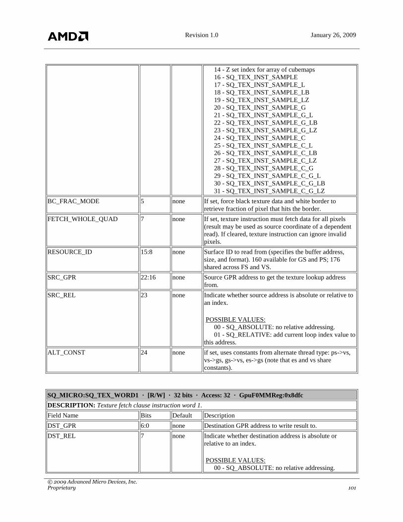
Revision 1.0 January 26, 2009
© 2009 Advanced Micro Devices, Inc. Proprietary 101
14 - Z set index for array of cubemaps
16 - SQ_TEX_INST_SAMPLE
17 - SQ_TEX_INST_SAMPLE_L
18 - SQ_TEX_INST_SAMPLE_LB
19 - SQ_TEX_INST_SAMPLE_LZ
20 - SQ_TEX_INST_SAMPLE_G
21 - SQ_TEX_INST_SAMPLE_G_L
22 - SQ_TEX_INST_SAMPLE_G_LB
23 - SQ_TEX_INST_SAMPLE_G_LZ
24 - SQ_TEX_INST_SAMPLE_C
25 - SQ_TEX_INST_SAMPLE_C_L
26 - SQ_TEX_INST_SAMPLE_C_LB
27 - SQ_TEX_INST_SAMPLE_C_LZ
28 - SQ_TEX_INST_SAMPLE_C_G
29 - SQ_TEX_INST_SAMPLE_C_G_L
30 - SQ_TEX_INST_SAMPLE_C_G_LB
31 - SQ_TEX_INST_SAMPLE_C_G_LZ
BC_FRAC_MODE 5 none If set, force black texture data and white border to
retrieve fraction of pixel that hits the border.
FETCH_WHOLE_QUAD 7 none If set, texture instruction must fetch data for all pixels
(result may be used as source coordinate of a dependent
read). If cleared, texture instruction can ignore invalid
pixels.
RESOURCE_ID 15:8 none Surface ID to read from (specifies the buffer address,
size, and format). 160 available for GS and PS; 176
shared across FS and VS.
SRC_GPR 22:16 none Source GPR address to get the texture lookup address
from.
SRC_REL 23 none Indicate whether source address is absolute or relative to
an index.
POSSIBLE VALUES:
00 - SQ_ABSOLUTE: no relative addressing.
01 - SQ_RELATIVE: add current loop index value to
this address.
ALT_CONST 24 none if set, uses constants from alternate thread type: ps->vs,
vs->gs, gs->vs, es->gs (note that es and vs share
constants).
SQ_MICRO:SQ_TEX_WORD1 · [R/W] · 32 bits · Access: 32 · GpuF0MMReg:0x8dfc
DESCRIPTION: Texture fetch clause instruction word 1.
Field Name Bits Default Description
DST_GPR 6:0 none Destination GPR address to write result to.
DST_REL 7 none Indicate whether destination address is absolute or
relative to an index.
POSSIBLE VALUES:
00 - SQ_ABSOLUTE: no relative addressing.
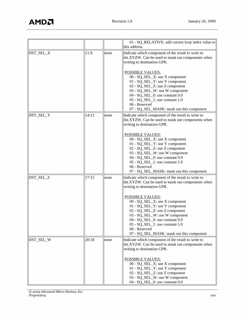
Revision 1.0 January 26, 2009
© 2009 Advanced Micro Devices, Inc. Proprietary 102
01 - SQ_RELATIVE: add current loop index value to
this address.
DST_SEL_X 11:9 none Indicate which component of the result to write to
dst.XYZW. Can be used to mask out components when
writing to destination GPR.
POSSIBLE VALUES:
00 - SQ_SEL_X: use X component
01 - SQ_SEL_Y: use Y component
02 - SQ_SEL_Z: use Z component
03 - SQ_SEL_W: use W component
04 - SQ_SEL_0: use constant 0.0
05 - SQ_SEL_1: use constant 1.0
06 - Reserved
07 - SQ_SEL_MASK: mask out this component
DST_SEL_Y 14:12 none Indicate which component of the result to write to
dst.XYZW. Can be used to mask out components when
writing to destination GPR.
POSSIBLE VALUES:
00 - SQ_SEL_X: use X component
01 - SQ_SEL_Y: use Y component
02 - SQ_SEL_Z: use Z component
03 - SQ_SEL_W: use W component
04 - SQ_SEL_0: use constant 0.0
05 - SQ_SEL_1: use constant 1.0
06 - Reserved
07 - SQ_SEL_MASK: mask out this component
DST_SEL_Z 17:15 none Indicate which component of the result to write to
dst.XYZW. Can be used to mask out components when
writing to destination GPR.
POSSIBLE VALUES:
00 - SQ_SEL_X: use X component
01 - SQ_SEL_Y: use Y component
02 - SQ_SEL_Z: use Z component
03 - SQ_SEL_W: use W component
04 - SQ_SEL_0: use constant 0.0
05 - SQ_SEL_1: use constant 1.0
06 - Reserved
07 - SQ_SEL_MASK: mask out this component
DST_SEL_W 20:18 none Indicate which component of the result to write to
dst.XYZW. Can be used to mask out components when
writing to destination GPR.
POSSIBLE VALUES:
00 - SQ_SEL_X: use X component
01 - SQ_SEL_Y: use Y component
02 - SQ_SEL_Z: use Z component
03 - SQ_SEL_W: use W component
04 - SQ_SEL_0: use constant 0.0
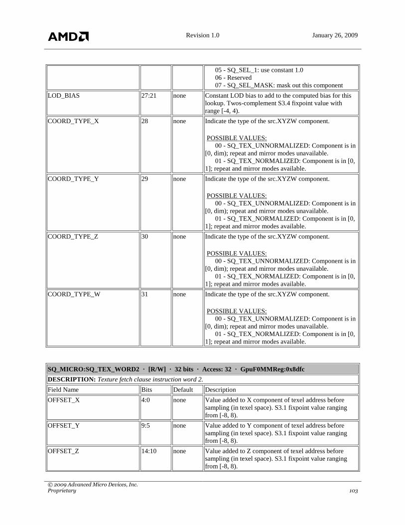
Revision 1.0 January 26, 2009
© 2009 Advanced Micro Devices, Inc. Proprietary 103
05 - SQ_SEL_1: use constant 1.0
06 - Reserved
07 - SQ_SEL_MASK: mask out this component
LOD_BIAS 27:21 none Constant LOD bias to add to the computed bias for this
lookup. Twos-complement S3.4 fixpoint value with
range [-4, 4).
COORD_TYPE_X 28 none Indicate the type of the src.XYZW component.
POSSIBLE VALUES:
00 - SQ_TEX_UNNORMALIZED: Component is in
[0, dim); repeat and mirror modes unavailable.
01 - SQ_TEX_NORMALIZED: Component is in [0,
1]; repeat and mirror modes available.
COORD_TYPE_Y 29 none Indicate the type of the src.XYZW component.
POSSIBLE VALUES:
00 - SQ_TEX_UNNORMALIZED: Component is in
[0, dim); repeat and mirror modes unavailable.
01 - SQ_TEX_NORMALIZED: Component is in [0,
1]; repeat and mirror modes available.
COORD_TYPE_Z 30 none Indicate the type of the src.XYZW component.
POSSIBLE VALUES:
00 - SQ_TEX_UNNORMALIZED: Component is in
[0, dim); repeat and mirror modes unavailable.
01 - SQ_TEX_NORMALIZED: Component is in [0,
1]; repeat and mirror modes available.
COORD_TYPE_W 31 none Indicate the type of the src.XYZW component.
POSSIBLE VALUES:
00 - SQ_TEX_UNNORMALIZED: Component is in
[0, dim); repeat and mirror modes unavailable.
01 - SQ_TEX_NORMALIZED: Component is in [0,
1]; repeat and mirror modes available.
SQ_MICRO:SQ_TEX_WORD2 · [R/W] · 32 bits · Access: 32 · GpuF0MMReg:0x8dfc
DESCRIPTION: Texture fetch clause instruction word 2.
Field Name Bits Default Description
OFFSET_X 4:0 none Value added to X component of texel address before
sampling (in texel space). S3.1 fixpoint value ranging
from [-8, 8).
OFFSET_Y 9:5 none Value added to Y component of texel address before
sampling (in texel space). S3.1 fixpoint value ranging
from [-8, 8).
OFFSET_Z 14:10 none Value added to Z component of texel address before
sampling (in texel space). S3.1 fixpoint value ranging
from [-8, 8).

Revision 1.0 January 26, 2009
© 2009 Advanced Micro Devices, Inc. Proprietary 104
SAMPLER_ID 19:15 none Sampler ID to use (specifies filter options, etc.). Value in
the range [0, 17].
SRC_SEL_X 22:20 none Indicate component source for src.XYZW.
POSSIBLE VALUES:
00 - SQ_SEL_X: use X component
01 - SQ_SEL_Y: use Y component
02 - SQ_SEL_Z: use Z component
03 - SQ_SEL_W: use W component
04 - SQ_SEL_0: use constant 0.0
05 - SQ_SEL_1: use constant 1.0
SRC_SEL_Y 25:23 none Indicate component source for src.XYZW.
POSSIBLE VALUES:
00 - SQ_SEL_X: use X component
01 - SQ_SEL_Y: use Y component
02 - SQ_SEL_Z: use Z component
03 - SQ_SEL_W: use W component
04 - SQ_SEL_0: use constant 0.0
05 - SQ_SEL_1: use constant 1.0
SRC_SEL_Z 28:26 none Indicate component source for src.XYZW.
POSSIBLE VALUES:
00 - SQ_SEL_X: use X component
01 - SQ_SEL_Y: use Y component
02 - SQ_SEL_Z: use Z component
03 - SQ_SEL_W: use W component
04 - SQ_SEL_0: use constant 0.0
05 - SQ_SEL_1: use constant 1.0
SRC_SEL_W 31:29 none Indicate component source for src.XYZW.
POSSIBLE VALUES:
00 - SQ_SEL_X: use X component
01 - SQ_SEL_Y: use Y component
02 - SQ_SEL_Z: use Z component
03 - SQ_SEL_W: use W component
04 - SQ_SEL_0: use constant 0.0
05 - SQ_SEL_1: use constant 1.0

Revision 1.0 January 26, 2009
© 2009 Advanced Micro Devices, Inc. Proprietary 105
6. Shader Vertex Resource Constants
SQ:SQ_VTX_CONSTANT_WORD0_0 · [R/W] · 32 bits · Access: 32 · GpuF0MMReg:0x38000
Field Name Bits Default Description
BASE_ADDRESS 31:0 0x0
SQ:SQ_VTX_CONSTANT_WORD1_0 · [R/W] · 32 bits · Access: 32 · GpuF0MMReg:0x38004
Field Name Bits Default Description
SIZE 31:0 0x0
SQ:SQ_VTX_CONSTANT_WORD2_0 · [R/W] · 32 bits · Access: 32 · GpuF0MMReg:0x38008
Field Name Bits Default Description
BASE_ADDRESS_HI 7:0 0x0
STRIDE 18:8 0x0
CLAMP_X 19 0x0 POSSIBLE VALUES:
00 - SQ_VTX_CLAMP_ZERO: clamp to zero
(0x00000000).
01 - SQ_VTX_CLAMP_NAN: clamp to NaN
(0xffc00000).
DATA_FORMAT 25:20 0x0
NUM_FORMAT_ALL 27:26 0x0 POSSIBLE VALUES:
00 - SQ_NUM_FORMAT_NORM: repeating
fraction number (0.N) with range [0, 1] if unsigned, or [-
1, 1] if signed.
01 - SQ_NUM_FORMAT_INT: integer number
(N.0) with range [0, 2^N] if unsigned, or [-2^M, 2^M] if
signed (M = N - 1).
02 - SQ_NUM_FORMAT_SCALED: integer
number stored as a S23E8 floating-point representation
(1 == 0x3f800000).
FORMAT_COMP_ALL 28 0x0 POSSIBLE VALUES:
00 - SQ_FORMAT_COMP_UNSIGNED
01 - SQ_FORMAT_COMP_SIGNED
SRF_MODE_ALL 29 0x0 POSSIBLE VALUES:
00 -
SQ_SRF_MODE_ZERO_CLAMP_MINUS_ONE:
representation with two -1 representations (one is slightly
past -1 but clamped).
01 - SQ_SRF_MODE_NO_ZERO: OpenGL format
lacking representation for 0.
ENDIAN_SWAP 31:30 0x0 POSSIBLE VALUES:
00 - SQ_ENDIAN_NONE: no endian swap (XOR by
0)
01 - SQ_ENDIAN_8IN16: 8 bit swap in 16 bit word
(XOR by 1): AABBCCDD -> BBAADDCC

Revision 1.0 January 26, 2009
© 2009 Advanced Micro Devices, Inc. Proprietary 106
02 - SQ_ENDIAN_8IN32: 8 bit swap in 32 bit word
(XOR by 3): AABBCCDD -> DDCCBBAA
SQ:SQ_VTX_CONSTANT_WORD3_0 · [R/W] · 32 bits · Access: 32 · GpuF0MMReg:0x3800c
Field Name Bits Default Description
MEM_REQUEST_SIZE 1:0 0x0
SQ:SQ_VTX_CONSTANT_WORD6_0 · [R/W] · 32 bits · Access: 32 · GpuF0MMReg:0x38018
Field Name Bits Default Description
TYPE 31:30 0x0 POSSIBLE VALUES:
00 - SQ_TEX_VTX_INVALID_TEXTURE
01 - SQ_TEX_VTX_INVALID_BUFFER
02 - SQ_TEX_VTX_VALID_TEXTURE
03 - SQ_TEX_VTX_VALID_BUFFER

Revision 1.0 January 26, 2009
© 2009 Advanced Micro Devices, Inc. Proprietary 107
7. Shader Texture Resource Constants
SQ:SQ_TEX_RESOURCE_WORD0_0 · [R/W] · 32 bits · Access: 32 · GpuF0MMReg:0x38000
Field Name Bits Default Description
DIM 2:0 0x0 POSSIBLE VALUES:
00 - SQ_TEX_DIM_1D
01 - SQ_TEX_DIM_2D
02 - SQ_TEX_DIM_3D
03 - SQ_TEX_DIM_CUBEMAP
04 - SQ_TEX_DIM_1D_ARRAY
05 - SQ_TEX_DIM_2D_ARRAY
06 - SQ_TEX_DIM_2D_MSAA
07 - SQ_TEX_DIM_2D_ARRAY_MSAA
TILE_MODE 6:3 0x0
TILE_TYPE 7 0x0
PITCH 18:8 0x0
TEX_WIDTH 31:19 0x0
SQ:SQ_TEX_RESOURCE_WORD1_0 · [R/W] · 32 bits · Access: 32 · GpuF0MMReg:0x38004
Field Name Bits Default Description
TEX_HEIGHT 12:0 0x0
TEX_DEPTH 25:13 0x0
DATA_FORMAT 31:26 0x0
SQ:SQ_TEX_RESOURCE_WORD2_0 · [R/W] · 32 bits · Access: 32 · GpuF0MMReg:0x38008
Field Name Bits Default Description
BASE_ADDRESS 31:0 0x0
SQ:SQ_TEX_RESOURCE_WORD3_0 · [R/W] · 32 bits · Access: 32 · GpuF0MMReg:0x3800c
Field Name Bits Default Description
MIP_ADDRESS 31:0 0x0
SQ:SQ_TEX_RESOURCE_WORD4_0 · [R/W] · 32 bits · Access: 32 · GpuF0MMReg:0x38010
Field Name Bits Default Description
FORMAT_COMP_X 1:0 0x0 POSSIBLE VALUES:
00 - SQ_FORMAT_COMP_UNSIGNED
01 - SQ_FORMAT_COMP_SIGNED
02 - SQ_FORMAT_COMP_UNSIGNED_BIASED
FORMAT_COMP_Y 3:2 0x0 POSSIBLE VALUES:
00 - SQ_FORMAT_COMP_UNSIGNED
01 - SQ_FORMAT_COMP_SIGNED

Revision 1.0 January 26, 2009
© 2009 Advanced Micro Devices, Inc. Proprietary 108
02 - SQ_FORMAT_COMP_UNSIGNED_BIASED
FORMAT_COMP_Z 5:4 0x0 POSSIBLE VALUES:
00 - SQ_FORMAT_COMP_UNSIGNED
01 - SQ_FORMAT_COMP_SIGNED
02 - SQ_FORMAT_COMP_UNSIGNED_BIASED
FORMAT_COMP_W 7:6 0x0 POSSIBLE VALUES:
00 - SQ_FORMAT_COMP_UNSIGNED
01 - SQ_FORMAT_COMP_SIGNED
02 - SQ_FORMAT_COMP_UNSIGNED_BIASED
NUM_FORMAT_ALL 9:8 0x0 POSSIBLE VALUES:
00 - SQ_NUM_FORMAT_NORM: repeating
fraction number (0.N) with range [0, 1] if unsigned, or [-
1, 1] if signed.
01 - SQ_NUM_FORMAT_INT: integer number
(N.0) with range [0, 2^N] if unsigned, or [-2^M, 2^M] if
signed (M = N - 1).
02 - SQ_NUM_FORMAT_SCALED: integer
number stored as a S23E8 floating-point representation
(1 == 0x3f800000).
SRF_MODE_ALL 10 0x0 POSSIBLE VALUES:
00 -
SQ_SRF_MODE_ZERO_CLAMP_MINUS_ONE:
representation with two -1 representations (one is slightly
past -1 but clamped).
01 - SQ_SRF_MODE_NO_ZERO: OpenGL format
lacking representation for 0.
FORCE_DEGAMMA 11 0x0
ENDIAN_SWAP 13:12 0x0 POSSIBLE VALUES:
00 - SQ_ENDIAN_NONE: no endian swap (XOR by
0)
01 - SQ_ENDIAN_8IN16: 8 bit swap in 16 bit word
(XOR by 1): AABBCCDD -> BBAADDCC
02 - SQ_ENDIAN_8IN32: 8 bit swap in 32 bit word
(XOR by 3): AABBCCDD -> DDCCBBAA
REQUEST_SIZE 15:14 0x0
DST_SEL_X 18:16 0x0 POSSIBLE VALUES:
00 - SQ_SEL_X: use X component
01 - SQ_SEL_Y: use Y component
02 - SQ_SEL_Z: use Z component
03 - SQ_SEL_W: use W component
04 - SQ_SEL_0: use constant 0.0
05 - SQ_SEL_1: use constant 1.0
DST_SEL_Y 21:19 0x0 POSSIBLE VALUES:
00 - SQ_SEL_X: use X component
01 - SQ_SEL_Y: use Y component
02 - SQ_SEL_Z: use Z component
03 - SQ_SEL_W: use W component
04 - SQ_SEL_0: use constant 0.0
05 - SQ_SEL_1: use constant 1.0
DST_SEL_Z 24:22 0x0 POSSIBLE VALUES:
Revision 1.0 January 26, 2009
© 2009 Advanced Micro Devices, Inc. Proprietary 109
00 - SQ_SEL_X: use X component
01 - SQ_SEL_Y: use Y component
02 - SQ_SEL_Z: use Z component
03 - SQ_SEL_W: use W component
04 - SQ_SEL_0: use constant 0.0
05 - SQ_SEL_1: use constant 1.0
DST_SEL_W 27:25 0x0 POSSIBLE VALUES:
00 - SQ_SEL_X: use X component
01 - SQ_SEL_Y: use Y component
02 - SQ_SEL_Z: use Z component
03 - SQ_SEL_W: use W component
04 - SQ_SEL_0: use constant 0.0
05 - SQ_SEL_1: use constant 1.0
BASE_LEVEL 31:28 0x0
SQ:SQ_TEX_RESOURCE_WORD5_0 · [R/W] · 32 bits · Access: 32 · GpuF0MMReg:0x38014
Field Name Bits Default Description
LAST_LEVEL 3:0 0x0
BASE_ARRAY 16:4 0x0
LAST_ARRAY 29:17 0x0
Reserved 31:30 0x0 Set to 0
SQ:SQ_TEX_RESOURCE_WORD6_0 · [R/W] · 32 bits · Access: 32 · GpuF0MMReg:0x38018
Field Name Bits Default Description
MPEG_CLAMP 1:0 0x0 POSSIBLE VALUES:
00 - SQ_TEX_MPEG_CLAMP_OFF: no clamping
(FMT_16 is plain 16b fixed/normalized number).
01 - SQ_TEX_MPEG_9: consider FMT_16 as s9 in
LSBs, clamp range to [-256, 255).
02 - SQ_TEX_MPEG_10: mask bottom 6b of
FMT_16.
Reserved 4:2 0x0
PERF_MODULATION 7:5 0x0
INTERLACED 8 0x0
TYPE 31:30 0x0 POSSIBLE VALUES:
00 - SQ_TEX_VTX_INVALID_TEXTURE
01 - SQ_TEX_VTX_INVALID_BUFFER
02 - SQ_TEX_VTX_VALID_TEXTURE
03 - SQ_TEX_VTX_VALID_BUFFER
Revision 1.0 January 26, 2009
© 2009 Advanced Micro Devices, Inc. Proprietary 110
8. Shader Texture Sampler Constants
SQ:SQ_TEX_SAMPLER_WORD0_0 · [R/W] · 32 bits · Access: 32 · GpuF0MMReg:0x3c000
Field Name Bits Default Description
CLAMP_X 2:0 0x0 POSSIBLE VALUES:
00 - SQ_TEX_WRAP
01 - SQ_TEX_MIRROR
02 - SQ_TEX_CLAMP_LAST_TEXEL: [0,1]
normalized, [0,dimen] unnormalized
03 - SQ_TEX_MIRROR_ONCE_LAST_TEXEL: [-
1,1]
04 - SQ_TEX_CLAMP_HALF_BORDER: [0,1]
normalized, [0,dimen] unnormalized
05 - SQ_TEX_MIRROR_ONCE_HALF_BORDER:
[-1,1]
06 - SQ_TEX_CLAMP_BORDER: [0,1]
normalized, [0,dimen] unnormalized
07 - SQ_TEX_MIRROR_ONCE_BORDER: [-1,1]
CLAMP_Y 5:3 0x0 POSSIBLE VALUES:
00 - SQ_TEX_WRAP
01 - SQ_TEX_MIRROR
02 - SQ_TEX_CLAMP_LAST_TEXEL: [0,1]
normalized, [0,dimen] unnormalized
03 - SQ_TEX_MIRROR_ONCE_LAST_TEXEL: [-
1,1]
04 - SQ_TEX_CLAMP_HALF_BORDER: [0,1]
normalized, [0,dimen] unnormalized
05 - SQ_TEX_MIRROR_ONCE_HALF_BORDER:
[-1,1]
06 - SQ_TEX_CLAMP_BORDER: [0,1]
normalized, [0,dimen] unnormalized
07 - SQ_TEX_MIRROR_ONCE_BORDER: [-1,1]
CLAMP_Z 8:6 0x0 POSSIBLE VALUES:
00 - SQ_TEX_WRAP
01 - SQ_TEX_MIRROR
02 - SQ_TEX_CLAMP_LAST_TEXEL: [0,1]
normalized, [0,dimen] unnormalized
03 - SQ_TEX_MIRROR_ONCE_LAST_TEXEL: [-
1,1]
04 - SQ_TEX_CLAMP_HALF_BORDER: [0,1]
normalized, [0,dimen] unnormalized
05 - SQ_TEX_MIRROR_ONCE_HALF_BORDER:
[-1,1]
06 - SQ_TEX_CLAMP_BORDER: [0,1]
normalized, [0,dimen] unnormalized
07 - SQ_TEX_MIRROR_ONCE_BORDER: [-1,1]
XY_MAG_FILTER 11:9 0x0 POSSIBLE VALUES:
00 - SQ_TEX_XY_FILTER_POINT
01 - SQ_TEX_XY_FILTER_BILINEAR
02 - SQ_TEX_XY_FILTER_BICUBIC

Revision 1.0 January 26, 2009
© 2009 Advanced Micro Devices, Inc. Proprietary 111
XY_MIN_FILTER 14:12 0x0 POSSIBLE VALUES:
00 - SQ_TEX_XY_FILTER_POINT
01 - SQ_TEX_XY_FILTER_BILINEAR
02 - SQ_TEX_XY_FILTER_BICUBIC
Z_FILTER 16:15 0x0 POSSIBLE VALUES:
00 - SQ_TEX_Z_FILTER_NONE
01 - SQ_TEX_Z_FILTER_POINT
02 - SQ_TEX_Z_FILTER_LINEAR
MIP_FILTER 18:17 0x0 POSSIBLE VALUES:
00 - SQ_TEX_Z_FILTER_NONE
01 - SQ_TEX_Z_FILTER_POINT
02 - SQ_TEX_Z_FILTER_LINEAR
Reserved 21:19 0x0
BORDER_COLOR_TYPE 23:22 0x0 POSSIBLE VALUES:
00 -
SQ_TEX_BORDER_COLOR_TRANS_BLACK: (0.0,
0.0, 0.0, 0.0)
01 -
SQ_TEX_BORDER_COLOR_OPAQUE_BLACK:
(0.0, 0.0, 0.0, 1.0)
02 -
SQ_TEX_BORDER_COLOR_OPAQUE_WHITE: (1.0,
1.0, 1.0, 1.0)
03 - SQ_TEX_BORDER_COLOR_REGISTER: use
BORDER_COLOR_[XYZW]
POINT_SAMPLING_CLAMP 24 0x0
TEX_ARRAY_OVERRIDE 25 0x0
DEPTH_COMPARE_FUNCTION 28:26 0x0 POSSIBLE VALUES:
00 - SQ_TEX_DEPTH_COMPARE_NEVER:
always 0
01 - SQ_TEX_DEPTH_COMPARE_LESS: 1 if
incoming Z < fetched data
02 - SQ_TEX_DEPTH_COMPARE_EQUAL: 1 if
incoming Z == fetched data
03 - SQ_TEX_DEPTH_COMPARE_LESSEQUAL:
1 if incoming Z <= fetched data
04 - SQ_TEX_DEPTH_COMPARE_GREATER: 1
if incoming Z > fetched data
05 - SQ_TEX_DEPTH_COMPARE_NOTEQUAL:
1 if incoming Z != fetched data
06 -
SQ_TEX_DEPTH_COMPARE_GREATEREQUAL: 1
if incoming Z >= fetched data
07 - SQ_TEX_DEPTH_COMPARE_ALWAYS:
always 1
CHROMA_KEY 30:29 0x0 POSSIBLE VALUES:
00 - SQ_TEX_CHROMA_KEY_DISABLED: no
chroma keying
01 - SQ_TEX_CHROMA_KEY_KILL: returns

Revision 1.0 January 26, 2009
© 2009 Advanced Micro Devices, Inc. Proprietary 112
negative value if any texel matches chroma key
02 - SQ_TEX_CHROMA_KEY_BLEND: sets
matching texels to 0 before blending
LOD_USES_MINOR_AXIS 31 0x0
SQ:SQ_TEX_SAMPLER_WORD1_0 · [R/W] · 32 bits · Access: 32 · GpuF0MMReg:0x3c004
Field Name Bits Default Description
MIN_LOD 9:0 0x0
MAX_LOD 19:10 0x0
LOD_BIAS 31:20 0x0
SQ:SQ_TEX_SAMPLER_WORD2_0 · [R/W] · 32 bits · Access: 32 · GpuF0MMReg:0x3c008
Field Name Bits Default Description
LOD_BIAS_SEC 11:0 0x0
MC_COORD_TRUNCATE 12 0x0
FORCE_DEGAMMA 13 0x0
HIGH_PRECISION_FILTER 14 0x0
PERF_MIP 17:15 0x0
PERF_Z 19:18 0x0
Reserved 25:20 0x0
FETCH_4 26 0x0
SAMPLE_IS_PCF 27 0x0
TYPE 31 0x0

Revision 1.0 January 26, 2009
© 2009 Advanced Micro Devices, Inc. Proprietary 113
9. Shader ALU Constants
SQ:SQ_ALU_CONSTANT0_0 · [R/W] · 32 bits · Access: 32 · GpuF0MMReg:0x30000
DESCRIPTION: (64-state) ALU Constant store data for use in DX9 mode (DX10 mode uses the constant-cache
instead and this constant-file is not available). All four components of a constant must be written for that constant to
be updated - the physical write to the constant store only occurs after the fourth component has been written. The
first set of 256 constants (0-255) are reserved for the pixel shader (PS). The second set of 256 constants (256-511)
are reserved for the vertex shader (VS). None are available to the GS or ES.
Field Name Bits Default Description
X 31:0 0x0 Format is IEEE float
SQ:SQ_ALU_CONSTANT1_0 · [R/W] · 32 bits · Access: 32 · GpuF0MMReg:0x30004
Field Name Bits Default Description
Y 31:0 0x0 Format is IEEE float
SQ:SQ_ALU_CONSTANT2_0 · [R/W] · 32 bits · Access: 32 · GpuF0MMReg:0x30008
Field Name Bits Default Description
Z 31:0 0x0 Format is IEEE float
SQ:SQ_ALU_CONSTANT3_0 · [R/W] · 32 bits · Access: 32 · GpuF0MMReg:0x3000c
Field Name Bits Default Description
W 31:0 0x0 Format is IEEE float
SQ:SQ_BOOL_CONST_[0-2] · [R/W] · 32 bits · Access: 32 · GpuF0MMReg:0x3e380-0x3e388
DESCRIPTION: (64-state) DX9 Boolean constants - these are available as input to flow control instructions such
as `IF`.There are 96 boolean constants available - 32 bits for each of the PS, VS, and GS. First for PS, next for VS,
last for GS. The booleans are usable in both dx9 and dx10 modes.
Field Name Bits Default Description
BOOLEANS 31:0 0x0 32 one-bit booleans for static branching
SQ:SQ_LOOP_CONST_0 · [R/W] · 32 bits · Access: 32 · GpuF0MMReg:0x3e200
DESCRIPTION: (64-state) DX9 loop counter constants - these are used to define the behaviour of a programmed
loop. There are 96 loop counter constants available - 32 each for the PS, VS, and GS. First 32 for PS, next 32 for
VS, last 32 for GS. The loop counter is usable in both DX9 and DX10 modes. This version is used for
SQ_CF_INST_LOOP and SQ_CF_INST_LOOP_NO_AL statements.
Field Name Bits Default Description
COUNT 11:0 0x0 Total number of loop iterations (unsigned)
INIT 23:12 0x0 Initial value of loop counter AL (unsigned)
INC 31:24 0x0 Amount loop counter increments after each loop iteration
Revision 1.0 January 26, 2009
© 2009 Advanced Micro Devices, Inc. Proprietary 114
(signed)
SQ:SQ_LOOP_CONST_DX10_0 · [R/W] · 32 bits · Access: 32 · GpuF0MMReg:0x3e200
DESCRIPTION: (64-state) DX9 loop counter constants - these are used to define the behaviour of a programmed
loop. There are 96 loop counter constants available - 32 each for the PS, VS, and GS. First 32 for PS, next 32 for
VS, last 32 for GS. The loop counter is usable in both DX9 and DX10 modes. This version is used for
SQ_CF_INST_LOOP_DX10 statements.
Field Name Bits Default Description
COUNT 31:0 0x0 Total number of loop iterations (unsigned)
SQ:SQ_ALU_CONST_BUFFER_SIZE_GS_[0-15] · [R/W] · 32 bits · Access: 32 ·
GpuF0MMReg:0x281c0-0x281fc
DESCRIPTION: (8-state). Number of elements in this constant buffer [0..4096], in units of 16 constants (cache
lines). Associated with SQ_ALU_CONST_CACHE_GS_0. You must always write both CONST_BUFFER_SIZE and
CONST_CACHE, unless size=0 in which case you may write only size.
Field Name Bits Default Description
DATA 8:0 0x0 Number of constant buffer elements
SQ:SQ_ALU_CONST_BUFFER_SIZE_PS_[0-15] · [R/W] · 32 bits · Access: 32 ·
GpuF0MMReg:0x28140-0x2817c
DESCRIPTION: (8-state). Number of elements in this constant buffer [0..4096], in units of 16 constants (cache
lines). Associated with SQ_ALU_CONST_CACHE_PS_0. You must always write both CONST_BUFFER_SIZE and
CONST_CACHE, unless size=0 in which case you may write only size.
Field Name Bits Default Description
DATA 8:0 0x0 Number of constant buffer elements
SQ:SQ_ALU_CONST_BUFFER_SIZE_VS_[0-15] · [R/W] · 32 bits · Access: 32 ·
GpuF0MMReg:0x28180-0x281bc
DESCRIPTION: (8-state). Number of elements in this constant buffer [0..4096], in units of 16 constants (cache
lines). Associated with SQ_ALU_CONST_CACHE_VS_0. You must always write both CONST_BUFFER_SIZE and
CONST_CACHE, unless size=0 in which case you may write only size.
Field Name Bits Default Description
DATA 8:0 0x0 Number of constant buffer elements
SQ:SQ_ALU_CONST_CACHE_GS_[0-15] · [R/W] · 32 bits · Access: 32 · GpuF0MMReg:0x289c0-
0x289fc
DESCRIPTION: (8-state) Base address of constant-buffer #0 used by the constant cache, 256B aligned address
[39:8]. You must always write both CONST_BUFFER_SIZE and CONST_CACHE, unless size=0 in which case you
may write only size.
Field Name Bits Default Description

Revision 1.0 January 26, 2009
© 2009 Advanced Micro Devices, Inc. Proprietary 115
DATA 31:0 0x0 TBD
SQ:SQ_ALU_CONST_CACHE_PS_[0-15] · [R/W] · 32 bits · Access: 32 · GpuF0MMReg:0x28940-
0x2897c
DESCRIPTION: (8-state) Base address of constant-buffer #0 used by the constant cache, 256B aligned address
[39:8]. You must always write both CONST_BUFFER_SIZE and CONST_CACHE, unless size=0 in which case you
may write only size.
Field Name Bits Default Description
DATA 31:0 0x0 TBD
SQ:SQ_ALU_CONST_CACHE_VS_[0-15] · [R/W] · 32 bits · Access: 32 · GpuF0MMReg:0x28980-
0x289bc
DESCRIPTION: (8-state) Base address of constant-buffer #0 used by the constant cache, 256B aligned address
[39:8]. Used by both VS and ES shaders. You must always write both CONST_BUFFER_SIZE and
CONST_CACHE, unless size=0 in which case you may write only size.
Field Name Bits Default Description
DATA 31:0 0x0 TBD

Revision 1.0 January 26, 2009
© 2009 Advanced Micro Devices, Inc. Proprietary 116
10. Shader Program Setup Registers
SQ:SQ_PGM_CF_OFFSET_ES · [R/W] · 32 bits · Access: 32 · GpuF0MMReg:0x288d8
DESCRIPTION: (8-state) Memory offset from the program start (SQ_PGM_START_ES) of the (8-byte aligned)
entry point for the export shader (ES) program. This is the first CF instruction that each thread will execute.
Field Name Bits Default Description
PGM_CF_OFFSET 19:0 0x0 Format is [22:3]
SQ:SQ_PGM_CF_OFFSET_FS · [R/W] · 32 bits · Access: 32 · GpuF0MMReg:0x288dc
DESCRIPTION: (8-state) Memory offset from the program start (SQ_PGM_START_FS) of the (8-byte aligned)
entry point for the fetch shader (FS) program. This is the first CF instruction that each thread will execute.
Field Name Bits Default Description
PGM_CF_OFFSET 19:0 0x0 Format is [22:3]
SQ:SQ_PGM_CF_OFFSET_GS · [R/W] · 32 bits · Access: 32 · GpuF0MMReg:0x288d4
DESCRIPTION: (8-state) Memory offset from the program start (SQ_PGM_START_GS) of the (8-byte aligned)
entry point for the geometry shader (GS) program. This is the first CF instruction that each thread will execute.
Field Name Bits Default Description
PGM_CF_OFFSET 19:0 0x0 Format is [22:3]
SQ:SQ_PGM_CF_OFFSET_PS · [R/W] · 32 bits · Access: 32 · GpuF0MMReg:0x288cc
DESCRIPTION: (8-state) Memory offset from the program start (SQ_PGM_START_PS) of the (8-byte aligned)
entry point for the pixel shader (PS) program. This is the first CF instruction that each thread will execute.
Field Name Bits Default Description
PGM_CF_OFFSET 19:0 0x0 Format is [22:3]
SQ:SQ_PGM_CF_OFFSET_VS · [R/W] · 32 bits · Access: 32 · GpuF0MMReg:0x288d0
DESCRIPTION: (8-state) Memory offset from the program start (SQ_PGM_START_VS) of the (8-byte aligned)
entry point for the vertex shader (VS) program. This is the first CF instruction that each thread will execute.
Field Name Bits Default Description
PGM_CF_OFFSET 19:0 0x0 Format is [22:3]
SQ:SQ_PGM_EXPORTS_PS · [R/W] · 32 bits · Access: 32 · GpuF0MMReg:0x28854
DESCRIPTION: (8-state). Defines the exports from the Pixel Shader Program.
Field Name Bits Default Description
EXPORT_MODE 4:0 0x0 Pixel Shader export mode. bbbbz where bbbb is how
many color we export (0-8) and z is export z or not. It is
illegal to program this to all zeros.

Revision 1.0 January 26, 2009
© 2009 Advanced Micro Devices, Inc. Proprietary 117
SQ:SQ_PGM_RESOURCES_ES · [R/W] · 32 bits · Access: 32 · GpuF0MMReg:0x28890
DESCRIPTION: (8-state). Resource requirements to run the ES program. Can only read most recent version, not
all 8 states.
Field Name Bits Default Description
NUM_GPRS 7:0 0x0 number of GPRs required to run this program [0..127]
STACK_SIZE 15:8 0x0 number of stack entries needed [0..255]
DX10_CLAMP 21 0x0 DX10 clamp mode. (1 = dx10 mode, 0 = dx9 mode). This
applies to all shaders. This affects how the SP output
clamp treats NaN. See SP doc for details.
FETCH_CACHE_LINES 26:24 0x0 number of program cache lines to fetch on a cache miss,
up to the size of the program segment [1..8].
UNCACHED_FIRST_INST 28 0x0 Ensure that the first instruction is not read from the first
instruction cache. Should only be used for debugging if
there is a problem with the cache.
SQ:SQ_PGM_RESOURCES_FS · [R/W] · 32 bits · Access: 32 · GpuF0MMReg:0x288a4
DESCRIPTION: (8-state). Resource requirements to run the FS program. The FS shares with either the VS (gs-off)
or ES (gs-on) and performs a single allocation equal to the VS+FS or ES+FS resource requirements. The SPI
allocates stack space as (VS/ES + FS_stack_size) in the same manner as GPRs. Max_call_depth and
fetch_cache_lines will be inherited from the parent shader (VS or ES). Can only read most recent version, not all 8
states.
Field Name Bits Default Description
NUM_GPRS 7:0 0x0 number of GPRs required to run this program [0..127]
STACK_SIZE 15:8 0x0 number of stack entries needed [0..255]
DX10_CLAMP 21 0x0 DX10 clamp mode. (1 = dx10 mode, 0 = dx9 mode). This
applies to all shaders. This affects how the SP output
clamp treats NaN. See SP doc for details.
SQ:SQ_PGM_RESOURCES_GS · [R/W] · 32 bits · Access: 32 · GpuF0MMReg:0x2887c
DESCRIPTION: (8-state). Resource requirements to run the GS program. Can only read most recent version, not
all 8 states.
Field Name Bits Default Description
NUM_GPRS 7:0 0x0 number of GPRs required to run this program [0..127]
STACK_SIZE 15:8 0x0 number of stack entries needed [0..255]
DX10_CLAMP 21 0x0 DX10 clamp mode. (1 = dx10 mode, 0 = dx9 mode). This
applies to all shaders. This affects how the SP output
clamp treats NaN. See SP doc for details.
FETCH_CACHE_LINES 26:24 0x0 number of program cache lines to fetch on a cache miss,
up to the size of the program segment [1..8].
UNCACHED_FIRST_INST 28 0x0 Ensure that the first instruction is not read from the first
instruction cache. Should only be used for debugging if
there is a problem with the cache.

Revision 1.0 January 26, 2009
© 2009 Advanced Micro Devices, Inc. Proprietary 118
SQ:SQ_PGM_RESOURCES_PS · [R/W] · 32 bits · Access: 32 · GpuF0MMReg:0x28850
DESCRIPTION: (8-state). Resource requirements to run the PS program. Can only read most recent version, not
all 8 states.
Field Name Bits Default Description
NUM_GPRS 7:0 0x0 number of GPRs required to run this program [0..127]
STACK_SIZE 15:8 0x0 number of stack entries needed [0..255]
DX10_CLAMP 21 0x0 DX10 clamp mode. (1 = dx10 mode, 0 = dx9 mode). This
applies to all shaders. This affects how the SP output
clamp treats NaN. See SP doc for details.
FETCH_CACHE_LINES 26:24 0x0 number of program cache lines to fetch on a cache miss,
up to the size of the program segment [1..8].
UNCACHED_FIRST_INST 28 0x0 Ensure that the first instruction is not read from the first
instruction cache. Should only be used for debugging if
there is a problem with the cache. On R600 only: this bit
MUST be set due to a bug that is fixed in derivative parts.
CLAMP_CONSTS 31 0x0 Clamp ALU constants to [-1.0, 1.0]. Used for shader
versions below PS2.0. Applies only to Constant-file
constants (not literals) and only to const-file entries 0..7.
Other entries are never clamped.
SQ:SQ_PGM_RESOURCES_VS · [R/W] · 32 bits · Access: 32 · GpuF0MMReg:0x28868
DESCRIPTION: (8-state). Resource requirements to run the VS program. Can only read most recent version, not
all 8 states.
Field Name Bits Default Description
NUM_GPRS 7:0 0x0 number of GPRs required to run this program [0..127]
STACK_SIZE 15:8 0x0 number of stack entries needed [0..255]
DX10_CLAMP 21 0x0 DX10 clamp mode. (1 = dx10 mode, 0 = dx9 mode). This
applies to all shaders. This affects how the SP output
clamp treats NaN. See SP doc for details.
FETCH_CACHE_LINES 26:24 0x0 number of program cache lines to fetch on a cache miss,
up to the size of the program segment [1..8].
UNCACHED_FIRST_INST 28 0x0 Ensure that the first instruction is not read from the first
instruction cache. Should only be used for debugging if
there is a problem with the cache.
SQ:SQ_PGM_START_ES · [R/W] · 32 bits · Access: 32 · GpuF0MMReg:0x28880
DESCRIPTION: (8-state) Memory address of the (256-byte aligned) first CF instruction of the shader code for the
export shader (ES)
Field Name Bits Default Description
PGM_START 31:0 0x0 Format is [39:8]
SQ:SQ_PGM_START_FS · [R/W] · 32 bits · Access: 32 · GpuF0MMReg:0x28894
Revision 1.0 January 26, 2009
© 2009 Advanced Micro Devices, Inc. Proprietary 119
DESCRIPTION: (8-state) Memory address of the (256-byte aligned) first CF instruction of the shader code for the
fetch shader (FS)
Field Name Bits Default Description
PGM_START 31:0 0x0 Format is [39:8]
SQ:SQ_PGM_START_GS · [R/W] · 32 bits · Access: 32 · GpuF0MMReg:0x2886c
DESCRIPTION: (8-state) Memory address of the (256-byte aligned) first CF instruction of the shader code for the
geometry shader (GS)
Field Name Bits Default Description
PGM_START 31:0 0x0 Format is [39:8]
SQ:SQ_PGM_START_PS · [R/W] · 32 bits · Access: 32 · GpuF0MMReg:0x28840
DESCRIPTION: (8-state) Memory address of the (256-byte aligned) first CF instruction of the shader code for the
pixel shader (PS)
Field Name Bits Default Description
PGM_START 31:0 0x0 Format is [39:8]
SQ:SQ_PGM_START_VS · [R/W] · 32 bits · Access: 32 · GpuF0MMReg:0x28858
DESCRIPTION: (8-state) Memory address of the (256-byte aligned) first CF instruction of the shader code for the
vertex shader (VS)
Field Name Bits Default Description
PGM_START 31:0 0x0 Format is [39:8]

Revision 1.0 January 26, 2009
© 2009 Advanced Micro Devices, Inc. Proprietary 120
11. Shader Interpolator Registers
SPI:SPI_CONFIG_CNTL · [R/W] · 32 bits · Access: 32 · GpuF0MMReg:0x9100
Field Name Bits Default Description
GPR_WRITE_PRIORITY 4:0 0x0 POSSIBLE VALUES:
00 - Priority order (high to low) = VS, GS, ES, PS
01 - Priority order = VS, GS, PS, ES
02 - Priority order = VS, ES, GS, PS
03 - Priority order = VS, ES, PS, GS
04 - Priority order = VS, PS, GS, ES
05 - Priority order = VS, PS, ES, GS
06 - Priority order = GS, VS, ES, PS
07 - Priority order = GS, VS, PS, ES
08 - Priority order = GS, ES, VS, PS
09 - Priority order = GS, ES, PS, VS
10 - Priority order = GS, PS, VS, ES
11 - Priority order = GS, PS, ES, VS
12 - Priority order = ES, VS, GS, PS
13 - Priority order = ES, VS, PS, GS
14 - Priority order = ES, GS, VS, PS
15 - Priority order = ES, GS, PS, VS
16 - Priority order = ES, PS, VS, GS
17 - Priority order = ES, PS, GS, VS
18 - Priority order = PS, VS, GS, ES
19 - Priority order = PS, VS, ES, GS
20 - Priority order = PS, GS, VS, ES
21 - Priority order = PS, GS, ES, VS
22 - Priority order = PS, ES, VS, GS
23 - Priority order = PS, ES, GS, VS
DISABLE_INTERP_1 5 0x0 POSSIBLE VALUES:
00 - Use both interpolators and both of
SPI_SH_input0/1 (default)
01 - Disable interp1 and SPI_SH_input1
DEBUG_THREAD_TYPE_SEL 7:6 0x0 POSSIBLE VALUES:
00 - PS
01 - VS
02 - GS
03 - ES
DEBUG_GROUP_SEL 12:8 0x0
DEBUG_GRBM_OVERRIDE 13 0x0 POSSIBLE VALUES:
00 - Use dbg_common output to mux group_0
01 - Use DEBUG_GROUP_SEL setting to mux
group_0
SPI:SPI_CONFIG_CNTL_1 · [R/W] · 32 bits · Access: 32 · GpuF0MMReg:0x913c
Field Name Bits Default Description
VTX_DONE_DELAY 3:0 0x0 POSSIBLE VALUES:
00 - delay 10 clks (defalut, min value needed for
R600 config)
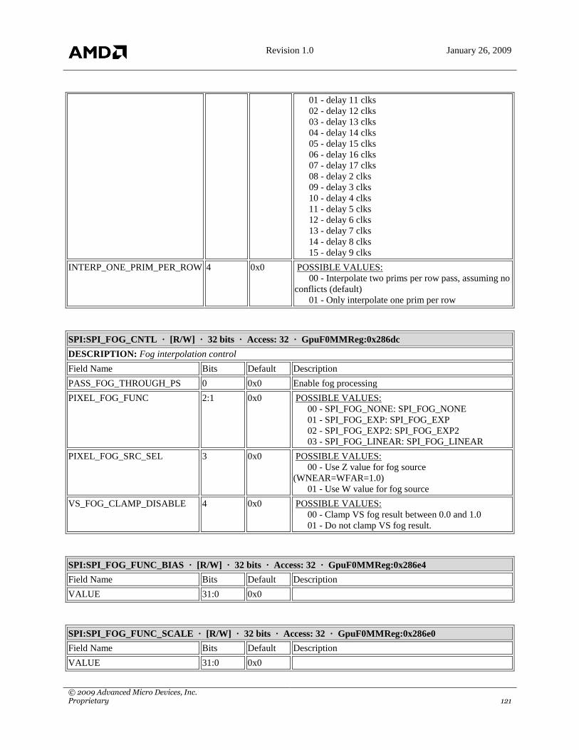
Revision 1.0 January 26, 2009
© 2009 Advanced Micro Devices, Inc. Proprietary 121
01 - delay 11 clks
02 - delay 12 clks
03 - delay 13 clks
04 - delay 14 clks
05 - delay 15 clks
06 - delay 16 clks
07 - delay 17 clks
08 - delay 2 clks
09 - delay 3 clks
10 - delay 4 clks
11 - delay 5 clks
12 - delay 6 clks
13 - delay 7 clks
14 - delay 8 clks
15 - delay 9 clks
INTERP_ONE_PRIM_PER_ROW 4 0x0 POSSIBLE VALUES:
00 - Interpolate two prims per row pass, assuming no
conflicts (default)
01 - Only interpolate one prim per row
SPI:SPI_FOG_CNTL · [R/W] · 32 bits · Access: 32 · GpuF0MMReg:0x286dc
DESCRIPTION: Fog interpolation control
Field Name Bits Default Description
PASS_FOG_THROUGH_PS 0 0x0 Enable fog processing
PIXEL_FOG_FUNC 2:1 0x0 POSSIBLE VALUES:
00 - SPI_FOG_NONE: SPI_FOG_NONE
01 - SPI_FOG_EXP: SPI_FOG_EXP
02 - SPI_FOG_EXP2: SPI_FOG_EXP2
03 - SPI_FOG_LINEAR: SPI_FOG_LINEAR
PIXEL_FOG_SRC_SEL 3 0x0 POSSIBLE VALUES:
00 - Use Z value for fog source
(WNEAR=WFAR=1.0)
01 - Use W value for fog source
VS_FOG_CLAMP_DISABLE 4 0x0 POSSIBLE VALUES:
00 - Clamp VS fog result between 0.0 and 1.0
01 - Do not clamp VS fog result.
SPI:SPI_FOG_FUNC_BIAS · [R/W] · 32 bits · Access: 32 · GpuF0MMReg:0x286e4
Field Name Bits Default Description
VALUE 31:0 0x0
SPI:SPI_FOG_FUNC_SCALE · [R/W] · 32 bits · Access: 32 · GpuF0MMReg:0x286e0
Field Name Bits Default Description
VALUE 31:0 0x0

Revision 1.0 January 26, 2009
© 2009 Advanced Micro Devices, Inc. Proprietary 122
SPI:SPI_INPUT_Z · [R/W] · 8 bits · Access: 8 · GpuF0MMReg:0x286d8
Field Name Bits Default Description
PROVIDE_Z_TO_SPI 0 0x0
SPI:SPI_INTERP_CONTROL_0 · [R/W] · 32 bits · Access: 32 · GpuF0MMReg:0x286d4
DESCRIPTION: Interpolator control settings
Field Name Bits Default Description
FLAT_SHADE_ENA 0 0x0 Global flat shade enable used in conjunction with per-
parameter flat shade control
PNT_SPRITE_ENA 1 0x0 Enable PT_SPRITE_TEX override for point primitives
PNT_SPRITE_OVRD_X 4:2 0x0 POSSIBLE VALUES:
00 - SPI_PNT_SPRITE_SEL_0: Override
component with 0.0f
01 - SPI_PNT_SPRITE_SEL_1: Override
component with 1.0f
02 - SPI_PNT_SPRITE_SEL_S: Override
component with S value
03 - SPI_PNT_SPRITE_SEL_T: Override
component with T value
04 - SPI_PNT_SPRITE_SEL_NONE: Keep
interpolated result
PNT_SPRITE_OVRD_Y 7:5 0x0 POSSIBLE VALUES:
00 - SPI_PNT_SPRITE_SEL_0: Override
component with 0.0f
01 - SPI_PNT_SPRITE_SEL_1: Override
component with 1.0f
02 - SPI_PNT_SPRITE_SEL_S: Override
component with S value
03 - SPI_PNT_SPRITE_SEL_T: Override
component with T value
04 - SPI_PNT_SPRITE_SEL_NONE: Keep
interpolated result
PNT_SPRITE_OVRD_Z 10:8 0x0 POSSIBLE VALUES:
00 - SPI_PNT_SPRITE_SEL_0: Override
component with 0.0f
01 - SPI_PNT_SPRITE_SEL_1: Override
component with 1.0f
02 - SPI_PNT_SPRITE_SEL_S: Override
component with S value
03 - SPI_PNT_SPRITE_SEL_T: Override
component with T value
04 - SPI_PNT_SPRITE_SEL_NONE: Keep
interpolated result
PNT_SPRITE_OVRD_W 13:11 0x0 POSSIBLE VALUES:
00 - SPI_PNT_SPRITE_SEL_0: Override
component with 0.0f

Revision 1.0 January 26, 2009
© 2009 Advanced Micro Devices, Inc. Proprietary 123
01 - SPI_PNT_SPRITE_SEL_1: Override
component with 1.0f
02 - SPI_PNT_SPRITE_SEL_S: Override
component with S value
03 - SPI_PNT_SPRITE_SEL_T: Override
component with T value
04 - SPI_PNT_SPRITE_SEL_NONE: Keep
interpolated result
PNT_SPRITE_TOP_1 14 0x0 POSSIBLE VALUES:
00 - T is 1.0 at bottom of primitive
01 - T is 1.0 at top of primitive
SPI:SPI_PS_INPUT_CNTL_[0-31] · [R/W] · 32 bits · Access: 32 · GpuF0MMReg:0x28644-0x286c0
DESCRIPTION: PS interpolator setttings for parameter 0
Field Name Bits Default Description
SEMANTIC 7:0 0x0 PS input semantic mapping
DEFAULT_VAL 9:8 0x0 Selects value to force into GPR if no semantic match
found
POSSIBLE VALUES:
00 - 0.0f, 0.0f, 0.0f, 0.0f
01 - 0.0f, 0.0f, 0.0f, 1.0f
02 - 1.0f, 1.0f, 1.0f, 0.0f
03 - 1,0f, 1.0f, 1.0f, 1.0f
FLAT_SHADE 10 0x0 Flat shade select
SEL_CENTROID 11 0x0 Use IJ data sampled at pixel centroid
SEL_LINEAR 12 0x0 Use IJ data from linear gradients
CYL_WRAP 16:13 0x0 4-bit cylindrical wrap control (1 bit per component)
PT_SPRITE_TEX 17 0x0 Override this parameter with texture coordinates if global
enable set and prim is a point
SEL_SAMPLE 18 0x0
SPI:SPI_PS_IN_CONTROL_0 · [R/W] · 32 bits · Access: 32 · GpuF0MMReg:0x286cc
DESCRIPTION: Interpolator control settings
Field Name Bits Default Description
NUM_INTERP 5:0 0x0 Number of parameters to interp (no minus 1). Does not
include fog, param_gen, or gen_indx, but should include
position and frontface
POSITION_ENA 8 0x0 Load per-pixel position into the PS
POSITION_CENTROID 9 0x0 Calculate per-pixel position at pixel centroid
POSITION_ADDR 14:10 0x0 Relative GPR address where position is loaded (0->31)
PARAM_GEN 18:15 0x0 Generate up to 4 sets of ST coordinates. Bit
0=persp/center, 1=persp/centroid, 2=linear/center,
3=linear/centroid
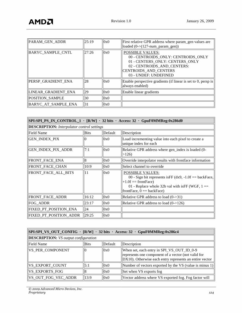
Revision 1.0 January 26, 2009
© 2009 Advanced Micro Devices, Inc. Proprietary 124
PARAM_GEN_ADDR 25:19 0x0 First relative GPR address where param_gen values are
loaded (0->(127-num_param_gen))
BARYC_SAMPLE_CNTL 27:26 0x0 POSSIBLE VALUES:
00 - CENTROIDS_ONLY: CENTROIDS_ONLY
01 - CENTERS_ONLY: CENTERS_ONLY
02 - CENTROIDS_AND_CENTERS:
CENTROIDS_AND_CENTERS
03 - UNDEF: UNDEFINED
PERSP_GRADIENT_ENA 28 0x0 Enable perspective gradients (if linear is set to 0, persp is
always enabled)
LINEAR_GRADIENT_ENA 29 0x0 Enable linear gradients
POSITION_SAMPLE 30 0x0
BARYC_AT_SAMPLE_ENA 31 0x0
SPI:SPI_PS_IN_CONTROL_1 · [R/W] · 32 bits · Access: 32 · GpuF0MMReg:0x286d0
DESCRIPTION: Interpolator control settings
Field Name Bits Default Description
GEN_INDEX_PIX 0 0x0 Load incrementing value into each pixel to create a
unique index for each
GEN_INDEX_PIX_ADDR 7:1 0x0 Relative GPR address where gen_index is loaded (0-
>126)
FRONT_FACE_ENA 8 0x0 Override interpolator results with frontface information
FRONT_FACE_CHAN 10:9 0x0 Select channel to override
FRONT_FACE_ALL_BITS 11 0x0 POSSIBLE VALUES:
00 - Sign bit represents isFF (dx9, -1.0f == backFace,
+1.0f == frontFace)
01 - Replace whole 32b val with isFF (WGF, 1 ==
frontFace, 0 == backFace)
FRONT_FACE_ADDR 16:12 0x0 Relative GPR address to load (0->31)
FOG_ADDR 23:17 0x0 Relative GPR address to load (0->126)
FIXED_PT_POSITION_ENA 24 0x0
FIXED_PT_POSITION_ADDR 29:25 0x0
SPI:SPI_VS_OUT_CONFIG · [R/W] · 32 bits · Access: 32 · GpuF0MMReg:0x286c4
DESCRIPTION: VS output configuration
Field Name Bits Default Description
VS_PER_COMPONENT 0 0x0 When set, each entry in SPI_VS_OUT_ID_0-9
represents one component of a vector (not valid for
DX10). Otherwise each entry represents an entire vector
VS_EXPORT_COUNT 5:1 0x0 Number of vectors exported by the VS (value is minus 1)
VS_EXPORTS_FOG 8 0x0 Set when VS exports fog
VS_OUT_FOG_VEC_ADDR 13:9 0x0 Vector address where VS exported fog. Fog factor will

Revision 1.0 January 26, 2009
© 2009 Advanced Micro Devices, Inc. Proprietary 125
always be in the X channel
SPI:SPI_VS_OUT_ID_[0-9] · [R/W] · 32 bits · Access: 32 · GpuF0MMReg:0x28614-0x28638
DESCRIPTION: VS output semantic mapping for 4 components/vectors
Field Name Bits Default Description
SEMANTIC_0 7:0 0x0
SEMANTIC_1 15:8 0x0
SEMANTIC_2 23:16 0x0
SEMANTIC_3 31:24 0x0

Revision 1.0 January 26, 2009
© 2009 Advanced Micro Devices, Inc. Proprietary 126
12. Shader Export Registers
SX:SX_ALPHA_REF · [R/W] · 32 bits · Access: 32 · GpuF0MMReg:0x28438
Field Name Bits Default Description
ALPHA_REF 31:0 none Reference value for alpha test, which is specified in
IEEE floating point.
SX:SX_ALPHA_TEST_CONTROL · [R/W] · 32 bits · Access: 32 · GpuF0MMReg:0x28410
Field Name Bits Default Description
ALPHA_FUNC 2:0 none Specifies the function used to compare the fragment
alpha value (produced by the shader pipe) to
ALPHA_REF, the reference alpha value. The alpha test
passes (keeping the pixel) if frag_alpha OP alpha_ref is
true.
POSSIBLE VALUES:
00 - REF_NEVER: never pass
01 - REF_LESS: pass if left < right
02 - REF_EQUAL: pass if left = right
03 - REF_LEQUAL: pass if left <= right
04 - REF_GREATER: pass if left > right
05 - REF_NOTEQUAL: pass if left != right
06 - REF_GEQUAL: pass if left >= right
07 - REF_ALWAYS: always pass
ALPHA_TEST_ENABLE 3 none If alpha test is enabled, then a failed ALPHA_FUNC
comparison causes the pixel to be killed.
POSSIBLE VALUES:
00 - DISABLE: force ALPHA_FUNC to ALWAYS
01 - ENABLE: discard pixels that do not pass the
alpha test.
ALPHA_TEST_BYPASS 8 none Driver can st this bit to bypass the alpha test for surface
types that don`t support alpha testing.
POSSIBLE VALUES:
00 - DISABLE: discard pixels that do not pass the
alpha test.
01 - ENABLE: force ALPHA_FUNC to ALWAYS.
SX:SX_EXPORT_BUFFER_SIZES · [R/W] · 32 bits · Access: 32 · GpuF0MMReg:0x900c
DESCRIPTION: Register that defines export buffer ring sizes
Field Name Bits Default Description
COLOR_BUFFER_SIZE 7:0 0x1F Number of 4 line buffers -1 in color buffer. Each
memory buffer corresponds to 4 lines of 16*128 bits
elements. Minimum acceptable value of register field is
0xA.

Revision 1.0 January 26, 2009
© 2009 Advanced Micro Devices, Inc. Proprietary 127
POSITION_BUFFER_SIZE 15:8 0x3 Number of 4 line buffers -1 in position buffer. Each
memory buffer corresponds to 4 lines of 16*128 bits
elements. Minimum acceptable value of register field is
0x12.
SMX_BUFFER_SIZE 23:16 0x1F Number of 4 line buffers -1 in smx buffer. Each memory
buffer corresponds to 4 lines of 16*128 bits elements
SX:SX_MEMORY_EXPORT_BASE · [R/W] · 32 bits · Access: 32 · GpuF0MMReg:0x9010
DESCRIPTION: Defines the base address of the memory export. Only available if chip supports
GPU__GC__MEM_EXPORT_PRESENT
Field Name Bits Default Description
ADDRESS 31:0 0x0 256 byte aligned base address, SX will add 8`h0 at the
bottom to get byte address
SX:SX_MEMORY_EXPORT_SIZE · [R/W] · 32 bits · Access: 32 · GpuF0MMReg:0x9014
DESCRIPTION: Defines the aperture of the memory export. Only available if chip supports
GPU__GC__MEM_EXPORT_PRESENT
Field Name Bits Default Description
SIZE 31:0 0x0 If computed address minus base address is greater than
size, SX will clamp to Size - 1 dword and disable the
write. Read will happen at size - 1 dword
SX:SX_MISC · [R/W] · 32 bits · Access: 32 · GpuF0MMReg:0x28350
Field Name Bits Default Description
MULTIPASS 0 none POSSIBLE VALUES:
00 - Do not kill all primitives
01 - Kill all primitives

Revision 1.0 January 26, 2009
© 2009 Advanced Micro Devices, Inc. Proprietary 128
13. Cache Control Registers
SMX:SMX_DC_CTL0 · [R/W] · 32 bits · Access: 32 · GpuF0MMReg:0xa020
DESCRIPTION: Control settings for all Data Caches. These settings should only be changed when the SMX is
idle.
Field Name Bits Default Description
WR_GATHER_STREAM0 0 0x1 For Stream0 traffic, use write gather on a write miss. To
be used in the case when there will be many writes to
memory. This allows SMX to send writes directly to the
memory without having to first fetch the cache line from
memory to the data caches.
WR_GATHER_STREAM1 1 0x1 For Stream1 traffic, use write gather on a write miss. To
be used in the case when there will be many writes to
memory. This allows SMX to send writes directly to the
memory without having to first fetch the cache line from
memory to the data caches.
WR_GATHER_STREAM2 2 0x1 For Stream2 traffic, use write gather on a write miss. To
be used in the case when there will be many writes to
memory. This allows SMX to send writes directly to the
memory without having to first fetch the cache line from
memory to the data caches.
WR_GATHER_STREAM3 3 0x1 For Stream3 traffic, use write gather on a write miss. To
be used in the case when there will be many writes to
memory. This allows SMX to send writes directly to the
memory without having to first fetch the cache line from
memory to the data caches.
WR_GATHER_SCRATCH 4 0x1 For Scratch traffic, use write gather on a write miss. To
be used in the case when there will be many writes to
memory. This allows SMX to send writes directly to the
memory without having to first fetch the cache line from
memory to the data caches.
WR_GATHER_REDUC_BUF 5 0x1 For Reduction Buffer traffic, use write gather on a write
miss. To be used in the case when there will be many
writes to memory. This allows SMX to send writes
directly to the memory without having to first fetch the
cache line from memory to the data caches.
WR_GATHER_RING_BUF 6 0x1 For Ring Buffer traffic, use write gather on a write miss.
To be used in the case when there will be many writes to
memory. This allows SMX to send writes directly to the
memory without having to first fetch the cache line from
memory to the data caches.
WR_GATHER_F_BUF 7 0x1 For F Buffer traffic, use write gather on a write miss. To
be used in the case when there will be many writes to
memory. This allows SMX to send writes directly to the
memory without having to first fetch the cache line from
memory to the data caches.
DISABLE_CACHES 8 0x0 Disables all Data Caches and turns on the bypass path.
WARNING: Only write requests can be handled while
caches are disabled. Read requests will still go to

Revision 1.0 January 26, 2009
© 2009 Advanced Micro Devices, Inc. Proprietary 129
memory but read returns will be dropped by the SMX.
AUTO_FLUSH_INVAL_EN 10 0x0 Valid only if AUTO_FLUSH_EN is set. Will cause auto-
invalidate as well as auto-flush
AUTO_FLUSH_EN 11 0x1 Turn on Auto Flush of caches. All caches will
automatically flush after AUTO_FLUSH_CNT idle
cycles.
AUTO_FLUSH_CNT 27:12 0x2710 Nr of idle cycles after which all caches will
automatically flush.
MC_RD_STALL_FACTOR 29:28 0x1 How easily SMX will assert MC`s read info stall bit.
2`d3 = only if cache_ctl_op_fifo_stalled, 2`d2 = as in 2
and if any VFA is full, 2`d1 = as in 1 and if IB full, 2`d0
= SMX will never assert read info stall bit.
MC_WR_STALL_FACTOR 31:30 0x1 How easily SMX will assert MC`s write info stall bit.
2`d3 = only if MU`s L2 victim cache or wr req fifo
stalled, 2`d2 = as in 2 and if any VFA is full, 2`d1 = as in
1 and if IB full, 2`d0 = SMX will never assert write info
stall bit.
SMX:SMX_DC_CTL1 · [R/W] · 32 bits · Access: 32 · GpuF0MMReg:0xa024
DESCRIPTION: Control settings for all Data Caches. These settings should only be changed when the SMX is
idle.
Field Name Bits Default Description
OP_FIFO_SKID 6:0 0x1 Skid for Cache Operation Fifo. Must
be at least 1.
CACHE_LINE_SIZE 8 0x0 Selects between 32-byte (CL32) or
64-byte (CL64) size cache lines.
Note that CL64 has double the cache
line width but half the number of
cache lines as CL32. Since the SMX
MC write and read interfaces are
only 32 bytes wide, a 64 byte cache
line transfer takes 2 consecutive
cycles over the MC interface, this
makes more efficient use of MC
bandwidth.
POSSIBLE VALUES:
00 - CL32: 32 byte (256 bit)
Cache Line size
01 - CL64: 64 byte (512 bit)
Cache Line size
MULTI_FLUSH_MODE 9 0x1 Allows multiple outstanding flushes
to be in flight without stalling the
pipeline. Only for ES/GS Flush and
Flush and/or invalidate all events.
Multi-Flush mode does not exist in
RV630.
MULTI_FLUSH_REQ_ABORT_IDX_FIFO_SKID 13:10 0x1 Skid for Multi-Flush Engine`s Flush

Revision 1.0 January 26, 2009
© 2009 Advanced Micro Devices, Inc. Proprietary 130
Request Abort Index Fifo. Must be at
least 1.
DISABLE_WR_GATHER_RD_HIT_FORCE_EVICT 16 0x0 A Read hit of a write-gathering
cacheline forces it to first evict to
memory then read back to ensure
coherency. Setting this bit allows
you to read the line without evicting
it first, but coherency (of cache vs
memory) is not guaranteed.
DISABLE_WR_GATHER_RD_HIT_COMP_VLDS_CHECK 17 0x0 In a write-gathering cacheline, a read
tag check also checks if the comp
valid bits allow a read to be serviced
from cache, else it is evicted and
read back. Setting this bit disables
the comp valid checking forcing any
read hit to a write gathering
cacheline to evict to memory and
read back.
DISABLE_FLUSH_ES_ALSO_INVALS 18 0x0 A Flush ES event also invalidates all
ES lines in the caches. Disabling this
will reduce cache`s ability to process
incoming requests while flushing,
reducing performance.
DISABLE_FLUSH_GS_ALSO_INVALS 19 0x0 A Flush GS event also invalidates all
GS lines in the caches. Disabling this
will reduce cache`s ability to process
incoming requests while flushing,
reducing performance.
SMX:SMX_DC_CTL2 · [R/W] · 32 bits · Access: 32 · GpuF0MMReg:0xa028
DESCRIPTION: Operations on all Data Caches. These operations should only be done when the SMX is idle. The
register fields can be polled to check for completion of the operation
Field Name Bits Default Description
INVALIDATE_CACHES 0 0x0 Invalidates all lines in all Data Caches. This field will
stay at 1 until the operation is complete, after which it
will revert to 0.
CACHES_INVALID 1 0x1 READ-ONLY. All lines in all Data Caches are invalid,
i.e., the caches are empty.
CACHES_DIRTY 2 0x0 READ-ONLY. There are some dirty lines in the Data
Caches.
FLUSH_ALL 4 0x0 Flush all lines from all caches. This field will stay at 1
until the operation is complete, after which it will revert
to 0.
FLUSH_GS_THREADS 8 0x0 Flush all lines from all caches which come from
Geometry Shader threads. This field will stay at 1 until
the operation is complete, after which it will revert to 0.
FLUSH_ES_THREADS 9 0x0 Flush all lines from all caches which come from Export

Revision 1.0 January 26, 2009
© 2009 Advanced Micro Devices, Inc. Proprietary 131
Shader threads. This field will stay at 1 until the
operation is complete, after which it will revert to 0.
TP:VC_CNTL_STATUS · [R] · 32 bits · Access: 32 · GpuF0MMReg:0x9704
DESCRIPTION: Vertex Cache Status
Field Name Bits Default Description
RP_BUSY 0 none Vertex Cache Request Processor is Busy
RG_BUSY 1 none Vertex Cache Request Generator is Busy
VC_BUSY 2 none Vertex Cache is Busy
CLAMP_DETECT 3 none
TP:TC_CNTL · [R/W] · 32 bits · Access: 32 · GpuF0MMReg:0x9608
DESCRIPTION: Texture Cache Control - When used, TC must be idle or rendering artifacts can occur
Field Name Bits Default Description
FORCE_HIT 0 0x0
FORCE_MISS 1 0x0
L2_SIZE 8:5 0x0 L2 cache size, can be used to disable L2 completely.
RV630 default=128K ; RV610 default=0
POSSIBLE VALUES:
00 - 256K
01 - 224K
02 - 192K
03 - 160K
04 - 128K
05 - 96K
06 - 64K
07 - 32K
08 - 0
L2_DISABLE_LATE_HIT 9 0x0
DISABLE_VERT_PERF 10 0x0
DISABLE_INVAL_BUSY 11 0x0
DISABLE_INVAL_SAME_SURFACE 12 0x0
PARTITION_MODE 14:13 0x0 Default is no partitioning
POSSIBLE VALUES:
00 - Vertex: Full Cache ; Texture: Full Cache
01 - Vertex: 1/2 Cache ; Texture: 1/2 Cache
02 - Vertex: 1/4 Cache ; Texture: 3/4 Cache
MISS_ARB_MODE 15 0x0
HIT_ARB_MODE 16 0x0
DISABLE_WRITE_DELAY 17 0x0
HIT_FIFO_DEPTH 18 0x0

Revision 1.0 January 26, 2009
© 2009 Advanced Micro Devices, Inc. Proprietary 132
TP:TC_INVALIDATE · [R/W] · 32 bits · Access: 32 · GpuF0MMReg:0x9604
DESCRIPTION: Texture Cache Invalidate - When used, TC must be idle or rendering artifacts can occur
Field Name Bits Default Description
START
(Access: W)
0 0x0 Invalidate L1 and L2 caches
TP:TC_STATUS · [R/W] · 32 bits · Access: 32 · GpuF0MMReg:0x9600
DESCRIPTION: Texture Cache Status
Field Name Bits Default Description
TC_BUSY
(Access: R)
0 none Texture Cache busy

Revision 1.0 January 26, 2009
© 2009 Advanced Micro Devices, Inc. Proprietary 133
14. Texture Pipe Registers
TP:TD[0-3]_CNTL · [R/W] · 32 bits · Access: 32 · GpuF0MMReg:0x9494-0x94a0
DESCRIPTION: Texture Data 0 Control
Field Name Bits Default Description
ID_OVERRIDE 29:28 none Texture Data 0 ID Override
TP:TD[0-3]_STATUS · [R/W] · 32 bits · Access: 32 · GpuF0MMReg:0x94a4-0x94b0
DESCRIPTION: Texture Data 0 Status
Field Name Bits Default Description
BUSY
(Access: R)
31 none
TP:TD_CNTL · [R/W] · 32 bits · Access: 32 · GpuF0MMReg:0x9490
DESCRIPTION: Texture Data Common Control
Field Name Bits Default Description
SYNC_PHASE_SH 1:0 0x0
SYNC_PHASE_VC_SMX 5:4 0x0
TP:TD_FILTER4 · [R/W] · 32 bits · Access: 32 · GpuF0MMReg:0x9400
DESCRIPTION: FILTER4 Write Weights
Field Name Bits Default Description
WEIGHT_1 10:0 none Right (or Bottom) weight of pair: format s2.9 (range [-2,
2), with 9b of fraction).
WEIGHT_0 21:11 none Left (or Top) weight of pair: format s2.9 (range [-2, 2),
with 9b of fraction).
WEIGHT_PAIR 22 none Indicates which pair of weights is loaded. 0: Left (or
Top) pair 1: Right (or Bottom) pair
PHASE 26:23 none Indicates which of 9 phases is loaded.
DIRECTION 27 none Indicates whether to load the horizontal (Left+Right) or
vertical (Top+Bottom) weight pair. 0: Horizontal 1:
Vertical
TP:TD_FILTER4_[1-35] · [R/W] · 32 bits · Access: 32 · GpuF0MMReg:0x9404-0x948c
Field Name Bits Default Description
WEIGHT_1 10:0 none
WEIGHT_0 21:11 none

Revision 1.0 January 26, 2009
© 2009 Advanced Micro Devices, Inc. Proprietary 134
TP:TD_GS_SAMPLER[0-17]_BORDER_ALPHA · [R/W] · 32 bits · Access: 32 ·
GpuF0MMReg:0xa80c-0xa91c
Field Name Bits Default Description
BORDER_ALPHA 31:0 none
TP:TD_GS_SAMPLER[0-17]_BORDER_BLUE · [R/W] · 32 bits · Access: 32 · GpuF0MMReg:0xa808-
0xa918
Field Name Bits Default Description
BORDER_BLUE 31:0 none
TP:TD_GS_SAMPLER[0-17]_BORDER_GREEN · [R/W] · 32 bits · Access: 32 ·
GpuF0MMReg:0xa804-0xa914
Field Name Bits Default Description
BORDER_GREEN 31:0 none
TP:TD_GS_SAMPLER[0-17]_BORDER_RED · [R/W] · 32 bits · Access: 32 · GpuF0MMReg:0xa800-
0xa910
Field Name Bits Default Description
BORDER_RED 31:0 none
TP:TD_PS_SAMPLER[0-17]_BORDER_ALPHA · [R/W] · 32 bits · Access: 32 · GpuF0MMReg:0xa40c-
0xa51c
Field Name Bits Default Description
BORDER_ALPHA 31:0 none
TP:TD_PS_SAMPLER[0-17]_BORDER_BLUE · [R/W] · 32 bits · Access: 32 · GpuF0MMReg:0xa408-
0xa518
Field Name Bits Default Description
BORDER_BLUE 31:0 none
TP:TD_PS_SAMPLER[0-17]_BORDER_GREEN · [R/W] · 32 bits · Access: 32 ·
GpuF0MMReg:0xa404-0xa514
Field Name Bits Default Description
BORDER_GREEN 31:0 none
TP:TD_PS_SAMPLER[0-17]_BORDER_RED · [R/W] · 32 bits · Access: 32 · GpuF0MMReg:0xa400-
0xa510

Revision 1.0 January 26, 2009
© 2009 Advanced Micro Devices, Inc. Proprietary 135
Field Name Bits Default Description
BORDER_RED 31:0 none
TP:TD_PS_SAMPLER[0-17]_CLEARTYPE_KERNEL · [R/W] · 32 bits · Access: 32 ·
GpuF0MMReg:0xaa00-0xaa44
Field Name Bits Default Description
WIDTH 2:0 none
HEIGHT 5:3 none
TP:TD_VS_SAMPLER[0-17]_BORDER_ALPHA · [R/W] · 32 bits · Access: 32 ·
GpuF0MMReg:0xa60c-0xa71c
Field Name Bits Default Description
BORDER_ALPHA 31:0 none
TP:TD_VS_SAMPLER[0-17]_BORDER_BLUE · [R/W] · 32 bits · Access: 32 · GpuF0MMReg:0xa608-
0xa718
Field Name Bits Default Description
BORDER_BLUE 31:0 none
TP:TD_VS_SAMPLER[0-17]_BORDER_GREEN · [R/W] · 32 bits · Access: 32 ·
GpuF0MMReg:0xa604-0xa714
Field Name Bits Default Description
BORDER_GREEN 31:0 none
TP:TD_VS_SAMPLER[0-17]_BORDER_RED · [R/W] · 32 bits · Access: 32 · GpuF0MMReg:0xa600-
0xa710
Field Name Bits Default Description
BORDER_RED 31:0 none
TP:TA0_CNTL · [R/W] · 32 bits · Access: 32 · GpuF0MMReg:0x9510
DESCRIPTION: Texture Addresser 0 Control
Field Name Bits Default Description
ID_OVERRIDE 29:28 none Texture Addresser 0 ID Override
TP:TA0_STATUS · [R/W] · 32 bits · Access: 32 · GpuF0MMReg:0x9520
DESCRIPTION: Texture Addresser 0 Status

Revision 1.0 January 26, 2009
© 2009 Advanced Micro Devices, Inc. Proprietary 136
Field Name Bits Default Description
FG_PFIFO_EMPTYB
(Access: R)
12 none Gradient FIFO state, pipeline fifo not empty
FG_LFIFO_EMPTYB
(Access: R)
13 none Gradient FIFO state, latency fifo not empty
FG_SFIFO_EMPTYB
(Access: R)
14 none Gradient FIFO state, state fifo not empty
FL_PFIFO_EMPTYB
(Access: R)
16 none LOD FIFO state, pipeline fifo not empty
FL_LFIFO_EMPTYB
(Access: R)
17 none LOD FIFO state, latency fifo not empty
FL_SFIFO_EMPTYB
(Access: R)
18 none LOD FIFO state, state fifo not empty
FA_PFIFO_EMPTYB
(Access: R)
20 none Addresser FIFO state, pipeline fifo not empty
FA_LFIFO_EMPTYB
(Access: R)
21 none Addresser FIFO state, latency fifo not empty
FA_SFIFO_EMPTYB
(Access: R)
22 none Addresser FIFO state, state fifo not empty
IN_BUSY
(Access: R)
24 none Input/LOD(Deriv) busy
FG_BUSY
(Access: R)
25 none Gradient FIFO busy
Reserved 26 none
FL_BUSY
(Access: R)
27 none LOD FIFO busy
TA_BUSY
(Access: R)
28 none Addresser busy
FA_BUSY
(Access: R)
29 none Addresser FIFO busy
AL_BUSY
(Access: R)
30 none Aligner busy
BUSY
(Access: R)
31 none Global TA0 busy
TP:TA1_CNTL · [R/W] · 32 bits · Access: 32 · GpuF0MMReg:0x9514
DESCRIPTION: Texture Addresser 1 Control
Field Name Bits Default Description
ID_OVERRIDE 29:28 none Texture Addresser 1 ID Override
TP:TA1_STATUS · [R/W] · 32 bits · Access: 32 · GpuF0MMReg:0x9524
DESCRIPTION: Texture Addresser 1 Status
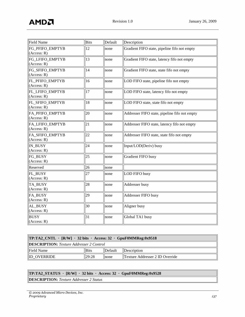
Revision 1.0 January 26, 2009
© 2009 Advanced Micro Devices, Inc. Proprietary 137
Field Name Bits Default Description
FG_PFIFO_EMPTYB
(Access: R)
12 none Gradient FIFO state, pipeline fifo not empty
FG_LFIFO_EMPTYB
(Access: R)
13 none Gradient FIFO state, latency fifo not empty
FG_SFIFO_EMPTYB
(Access: R)
14 none Gradient FIFO state, state fifo not empty
FL_PFIFO_EMPTYB
(Access: R)
16 none LOD FIFO state, pipeline fifo not empty
FL_LFIFO_EMPTYB
(Access: R)
17 none LOD FIFO state, latency fifo not empty
FL_SFIFO_EMPTYB
(Access: R)
18 none LOD FIFO state, state fifo not empty
FA_PFIFO_EMPTYB
(Access: R)
20 none Addresser FIFO state, pipeline fifo not empty
FA_LFIFO_EMPTYB
(Access: R)
21 none Addresser FIFO state, latency fifo not empty
FA_SFIFO_EMPTYB
(Access: R)
22 none Addresser FIFO state, state fifo not empty
IN_BUSY
(Access: R)
24 none Input/LOD(Deriv) busy
FG_BUSY
(Access: R)
25 none Gradient FIFO busy
Reserved 26 none
FL_BUSY
(Access: R)
27 none LOD FIFO busy
TA_BUSY
(Access: R)
28 none Addresser busy
FA_BUSY
(Access: R)
29 none Addresser FIFO busy
AL_BUSY
(Access: R)
30 none Aligner busy
BUSY
(Access: R)
31 none Global TA1 busy
TP:TA2_CNTL · [R/W] · 32 bits · Access: 32 · GpuF0MMReg:0x9518
DESCRIPTION: Texture Addresser 2 Control
Field Name Bits Default Description
ID_OVERRIDE 29:28 none Texture Addresser 2 ID Override
TP:TA2_STATUS · [R/W] · 32 bits · Access: 32 · GpuF0MMReg:0x9528
DESCRIPTION: Texture Addresser 2 Status
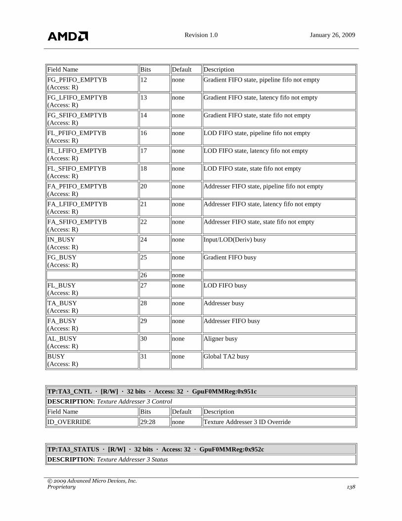
Revision 1.0 January 26, 2009
© 2009 Advanced Micro Devices, Inc. Proprietary 138
Field Name Bits Default Description
FG_PFIFO_EMPTYB
(Access: R)
12 none Gradient FIFO state, pipeline fifo not empty
FG_LFIFO_EMPTYB
(Access: R)
13 none Gradient FIFO state, latency fifo not empty
FG_SFIFO_EMPTYB
(Access: R)
14 none Gradient FIFO state, state fifo not empty
FL_PFIFO_EMPTYB
(Access: R)
16 none LOD FIFO state, pipeline fifo not empty
FL_LFIFO_EMPTYB
(Access: R)
17 none LOD FIFO state, latency fifo not empty
FL_SFIFO_EMPTYB
(Access: R)
18 none LOD FIFO state, state fifo not empty
FA_PFIFO_EMPTYB
(Access: R)
20 none Addresser FIFO state, pipeline fifo not empty
FA_LFIFO_EMPTYB
(Access: R)
21 none Addresser FIFO state, latency fifo not empty
FA_SFIFO_EMPTYB
(Access: R)
22 none Addresser FIFO state, state fifo not empty
IN_BUSY
(Access: R)
24 none Input/LOD(Deriv) busy
FG_BUSY
(Access: R)
25 none Gradient FIFO busy
26 none
FL_BUSY
(Access: R)
27 none LOD FIFO busy
TA_BUSY
(Access: R)
28 none Addresser busy
FA_BUSY
(Access: R)
29 none Addresser FIFO busy
AL_BUSY
(Access: R)
30 none Aligner busy
BUSY
(Access: R)
31 none Global TA2 busy
TP:TA3_CNTL · [R/W] · 32 bits · Access: 32 · GpuF0MMReg:0x951c
DESCRIPTION: Texture Addresser 3 Control
Field Name Bits Default Description
ID_OVERRIDE 29:28 none Texture Addresser 3 ID Override
TP:TA3_STATUS · [R/W] · 32 bits · Access: 32 · GpuF0MMReg:0x952c
DESCRIPTION: Texture Addresser 3 Status

Revision 1.0 January 26, 2009
© 2009 Advanced Micro Devices, Inc. Proprietary 139
Field Name Bits Default Description
FG_PFIFO_EMPTYB
(Access: R)
12 none Gradient FIFO state, pipeline fifo not empty
FG_LFIFO_EMPTYB
(Access: R)
13 none Gradient FIFO state, latency fifo not empty
FG_SFIFO_EMPTYB
(Access: R)
14 none Gradient FIFO state, state fifo not empty
FL_PFIFO_EMPTYB
(Access: R)
16 none LOD FIFO state, pipeline fifo not empty
FL_LFIFO_EMPTYB
(Access: R)
17 none LOD FIFO state, latency fifo not empty
FL_SFIFO_EMPTYB
(Access: R)
18 none LOD FIFO state, state fifo not empty
FA_PFIFO_EMPTYB
(Access: R)
20 none Addresser FIFO state, pipeline fifo not empty
FA_LFIFO_EMPTYB
(Access: R)
21 none Addresser FIFO state, latency fifo not empty
FA_SFIFO_EMPTYB
(Access: R)
22 none Addresser FIFO state, state fifo not empty
IN_BUSY
(Access: R)
24 none Input/LOD(Deriv) busy
FG_BUSY
(Access: R)
25 none Gradient FIFO busy
Reserved 26 none
FL_BUSY
(Access: R)
27 none LOD FIFO busy
TA_BUSY
(Access: R)
28 none Addresser busy
FA_BUSY
(Access: R)
29 none Addresser FIFO busy
AL_BUSY
(Access: R)
30 none Aligner busy
BUSY
(Access: R)
31 none Global TA3 busy
TP:TA_CNTL_AUX · [R/W] · 32 bits · Access: 32 · GpuF0MMReg:0x9508
DESCRIPTION: Texture Addresser Common Control
Field Name Bits Default Description
DISABLE_CUBE_WRAP 0 0x0 CubeMap Clamp Policy Override
POSSIBLE VALUES:
00 - Force Clamp X,Y policy to wrap for CubeMaps
01 - Allow other clamp modest
Reserved 1 0x0

Revision 1.0 January 26, 2009
© 2009 Advanced Micro Devices, Inc. Proprietary 140
SYNC_GRADIENT 24 0x1 Gradient synchronization mode
POSSIBLE VALUES:
00 - Gradient Sync on Instruction
01 - Gradient Sync on Phase
SYNC_WALKER 25 0x1 Walker synchronization mode
POSSIBLE VALUES:
00 - Walker Sync on Instruction
01 - Walker Sync on Phase
SYNC_ALIGNER 26 0x1 Aligner synchronization mode
POSSIBLE VALUES:
00 - Aligner Sync on Instruction
01 - Aligner Sync on Phase
BILINEAR_PRECISION 31 0x0 Bilinear precision setting
POSSIBLE VALUES:
00 - 6-bit bilinear weights always
01 - 8-bit bilinear weights if possible

Revision 1.0 January 26, 2009
© 2009 Advanced Micro Devices, Inc. Proprietary 141
15. Depth Buffer Registers
DB:DB_DEPTH_BASE · [R/W] · 32 bits · Access: 32 · GpuF0MMReg:0x2800c
Field Name Bits Default Description
BASE_256B 31:0 none Location of the first byte of the Depth surface in Device
Address Space, which must be 256 byte aligned. High
32-bits of 40-bit address.
DB:DB_DEPTH_CLEAR · [R/W] · 32 bits · Access: 32 · GpuF0MMReg:0x2802c
Field Name Bits Default Description
DEPTH_CLEAR 31:0 none Depth value when ZMASK==0, which indicates that the
tile has been cleared to the background depth. This
register holds a 32bit float value.
DB:DB_DEPTH_CONTROL · [R/W] · 32 bits · Access: 32 · GpuF0MMReg:0x28800
DESCRIPTION: This register controls depth and stencil tests.
Field Name Bits Default Description
STENCIL_ENABLE 0 none Enables stencil testing. If disabled, all pixels pass the
stencil test. If there is no stencil buffer this is treated as
disabled.
Z_ENABLE 1 none Enables depth testing. If disabled, all pixels pass the
depth test. If there is no depth buffer this is treated as
disabled.
Z_WRITE_ENABLE 2 none Enables writing to the depth buffer if the depth test
passes.
ZFUNC 6:4 none Specifies the function that compares the depth at each
sample in the fragment to the destination depth at the
corresponding sample point.
POSSIBLE VALUES:
00 - FRAG_NEVER: never pass
01 - FRAG_LESS: pass if fragment < dest
02 - FRAG_EQUAL: pass if fragment = dest
03 - FRAG_LEQUAL: pass if fragment <= dest
04 - FRAG_GREATER: pass if fragment > dest
05 - FRAG_NOTEQUAL: pass if fragment != dest
06 - FRAG_GEQUAL: pass if fragment >= dest
07 - FRAG_ALWAYS: always pass
BACKFACE_ENABLE 7 none If false, forces all quads to be stencil tested as frontface
quads.
STENCILFUNC 10:8 none Specifies the function that compares STENCILREF to
the destination stencil value for frontface quads. The
stencil test passes if ref OP dest is true.
POSSIBLE VALUES:

Revision 1.0 January 26, 2009
© 2009 Advanced Micro Devices, Inc. Proprietary 142
00 - REF_NEVER: never pass
01 - REF_LESS: pass if left < right
02 - REF_EQUAL: pass if left = right
03 - REF_LEQUAL: pass if left <= right
04 - REF_GREATER: pass if left > right
05 - REF_NOTEQUAL: pass if left != right
06 - REF_GEQUAL: pass if left >= right
07 - REF_ALWAYS: always pass
STENCILFAIL 13:11 none Specifies the stencil operation for frontface quads if the
stencil function fails.
POSSIBLE VALUES:
00 - STENCIL_KEEP: New value = Old Value
01 - STENCIL_ZERO: New value = 0
02 - STENCIL_REPLACE: New value =
STENCILREF
03 - STENCIL_INCR_CLAMP: New value++
(clamp)
04 - STENCIL_DECR_CLAMP: New value--
(clamp)
05 - STENCIL_INVERT: New value=~Old value
06 - STENCIL_INCR_WRAP: New value++ (wrap)
07 - STENCIL_DECR_WRAP: New value-- (wrap)
STENCILZPASS 16:14 none Specifies the stencil operation for frontface quads if the
stencil and depth functions both pass.
POSSIBLE VALUES:
00 - STENCIL_KEEP: New value = Old Value
01 - STENCIL_ZERO: New value = 0
02 - STENCIL_REPLACE: New value =
STENCILREF
03 - STENCIL_INCR_CLAMP: New value++
(clamp)
04 - STENCIL_DECR_CLAMP: New value--
(clamp)
05 - STENCIL_INVERT: New value=~Old value
06 - STENCIL_INCR_WRAP: New value++ (wrap)
07 - STENCIL_DECR_WRAP: New value-- (wrap)
STENCILZFAIL 19:17 none Specifies the stencil operation for frontface quads if the
stencil function passes and the depth function fails.
POSSIBLE VALUES:
00 - STENCIL_KEEP: New value = Old Value
01 - STENCIL_ZERO: New value = 0
02 - STENCIL_REPLACE: New value =
STENCILREF
03 - STENCIL_INCR_CLAMP: New value++
(clamp)
04 - STENCIL_DECR_CLAMP: New value--
(clamp)
05 - STENCIL_INVERT: New value=~Old value
06 - STENCIL_INCR_WRAP: New value++ (wrap)

Revision 1.0 January 26, 2009
© 2009 Advanced Micro Devices, Inc. Proprietary 143
07 - STENCIL_DECR_WRAP: New value-- (wrap)
STENCILFUNC_BF 22:20 none Specifies the function that compares STENCILREF_BF
to the destination stencil for backface quads. The stencil
test passes if ref OP dest is true.
POSSIBLE VALUES:
00 - REF_NEVER: never pass
01 - REF_LESS: pass if left < right
02 - REF_EQUAL: pass if left = right
03 - REF_LEQUAL: pass if left <= right
04 - REF_GREATER: pass if left > right
05 - REF_NOTEQUAL: pass if left != right
06 - REF_GEQUAL: pass if left >= right
07 - REF_ALWAYS: always pass
STENCILFAIL_BF 25:23 none Specifies the stencil operation for backface quads if the
stencil function fails.
POSSIBLE VALUES:
00 - STENCIL_KEEP: New value = Old Value
01 - STENCIL_ZERO: New value = 0
02 - STENCIL_REPLACE: New value =
STENCILREF
03 - STENCIL_INCR_CLAMP: New value++
(clamp)
04 - STENCIL_DECR_CLAMP: New value--
(clamp)
05 - STENCIL_INVERT: New value=~Old value
06 - STENCIL_INCR_WRAP: New value++ (wrap)
07 - STENCIL_DECR_WRAP: New value-- (wrap)
STENCILZPASS_BF 28:26 none Specifies the stencil operation for backface quads if the
stencil and depth functions both pass.
POSSIBLE VALUES:
00 - STENCIL_KEEP: New value = Old Value
01 - STENCIL_ZERO: New value = 0
02 - STENCIL_REPLACE: New value =
STENCILREF
03 - STENCIL_INCR_CLAMP: New value++
(clamp)
04 - STENCIL_DECR_CLAMP: New value--
(clamp)
05 - STENCIL_INVERT: New value=~Old value
06 - STENCIL_INCR_WRAP: New value++ (wrap)
07 - STENCIL_DECR_WRAP: New value-- (wrap)
STENCILZFAIL_BF 31:29 none Specifies the stencil operation for backface quads if the
stencil function passes and the depth function fails.
POSSIBLE VALUES:
00 - STENCIL_KEEP: New value = Old Value
01 - STENCIL_ZERO: New value = 0
02 - STENCIL_REPLACE: New value =

Revision 1.0 January 26, 2009
© 2009 Advanced Micro Devices, Inc. Proprietary 144
STENCILREF
03 - STENCIL_INCR_CLAMP: New value++
(clamp)
04 - STENCIL_DECR_CLAMP: New value--
(clamp)
05 - STENCIL_INVERT: New value=~Old value
06 - STENCIL_INCR_WRAP: New value++ (wrap)
07 - STENCIL_DECR_WRAP: New value-- (wrap)
DB:DB_DEPTH_INFO · [R/W] · 32 bits · Access: 32 · GpuF0MMReg:0x28010
Field Name Bits Default Description
FORMAT 2:0 none Specifies the size of the depth and stencil components
and whether depth is floating point.
POSSIBLE VALUES:
00 - DEPTH_INVALID: Depth and stencil surface
are not valid.
01 - DEPTH_16: UNORM 16-bit depth.
02 - DEPTH_X8_24: 24-bit UNORM depth and
invalid stencil surface.
03 - DEPTH_8_24: 24-bit UNORM depth and int
stencil.
04 - DEPTH_X8_24_FLOAT: 24-bit float depth and
invalid stencil surface.
05 - DEPTH_8_24_FLOAT: 24-bit float depth and
int stencil.
06 - DEPTH_32_FLOAT: 32-bit float depth.
07 - DEPTH_X24_8_32_FLOAT: 32-bit float depth
and int stencil.
READ_SIZE 3 none Specifies the read size: larger reads are more efficient for
AGP accesses, for example.
POSSIBLE VALUES:
00 - READ_256_BITS
01 - READ_512_BITS
ARRAY_MODE 18:15 none Specifies the tiling format for this array. DB does not
support values 0, 1, 3, 7, 11, 13, or 15.
POSSIBLE VALUES:
04 - ARRAY_2D_TILED_THIN1: Uses 8x8x1
macro-tiles
TILE_SURFACE_ENABLE 25 none Enables reading and writing of the htile data. If off
HiZ+S is off.
TILE_COMPACT 26 none If true, this surface is compacted to eliminate storage that
would be unused due to multi-chip supertiling. The
supertiling mode is specified in
PA_SC_MULTI_CHIP_CNTL. If this bit is set, then
MULTI_CHIP_SUPERTILE_ENABLE must be set in

Revision 1.0 January 26, 2009
© 2009 Advanced Micro Devices, Inc. Proprietary 145
PA_SC_MODE_CNTL.
ZRANGE_PRECISION 31 none 0 = ZMin is the base, generally set when doing a Z > test,
1 = ZMax is the base, set when generally using a Z <
test. The value used as base has full 14 bit precision. By
setting the base to Max culling has less error in a < test.
Can only be changed after a full surface clear.
DB:DB_DEPTH_SIZE · [R/W] · 32 bits · Access: 32 · GpuF0MMReg:0x28000
Field Name Bits Default Description
PITCH_TILE_MAX 9:0 none Width in 8x8 pixel tiles. (Pitch - 1)
SLICE_TILE_MAX 29:10 none Number of 8x8 pixel tiles until the next slice plus some
small number to be able to rotate the tile pattern. (Pitch -
1)
DB:DB_DEPTH_VIEW · [R/W] · 32 bits · Access: 32 · GpuF0MMReg:0x28004
DESCRIPTION: Selects slice index range for render target 0.
Field Name Bits Default Description
SLICE_START 10:0 none Specifies the starting slice number for this view. This
field is added to the RenderTargetArrayIndex to compute
the slice to render.
SLICE_MAX 23:13 none Specifies the maximum allowed Z slice index for this
resource, which is one less than the total number of
slices.
DB:DB_HTILE_DATA_BASE · [R/W] · 32 bits · Access: 32 · GpuF0MMReg:0x28014
Field Name Bits Default Description
BASE_256B 31:0 none Location of the first byte of the HTileData surface in
Device Address Space, which must be 256 byte aligned.
High 32-bits of 40-bit address. This surface contains the
HiZ data.
DB:DB_HTILE_SURFACE · [R/W] · 32 bits · Access: 32 · GpuF0MMReg:0x28d24
Field Name Bits Default Description
HTILE_WIDTH 0 none How many pixels wide each entry in the htile buffer
represents. 0 = 4, 1 = 8
HTILE_HEIGHT 1 none How many pixels high each entry in the htile buffer
represents. 0 = 4, 1 = 8
LINEAR 2 none Surface is stored linearly in swaths of 8 htiles high until
the surface is complete.
FULL_CACHE 3 none This htile buffer uses the entire htile cache.
HTILE_USES_PRELOAD_WIN 4 none If set, the htile surface dimensions will be that of the
Revision 1.0 January 26, 2009
© 2009 Advanced Micro Devices, Inc. Proprietary 146
preload window; otherwise, it will be that of the depth
buffer
PRELOAD 5 none Preload all data that fits as soon as room is available
once the VGT_DRAW_INITIATOR is seen on a
context.
PREFETCH_WIDTH 11:6 none The Prefetch window width. Prefetcher tries to keep this
window around the last rasterized htile in cache at all
times.
PREFETCH_HEIGHT 17:12 none The Prefetch window height. Prefetcher tries to keep this
window around the last rasterized htile in cache at all
times.
DB:DB_PREFETCH_LIMIT · [R/W] · 32 bits · Access: 32 · GpuF0MMReg:0x28d34
Field Name Bits Default Description
DEPTH_HEIGHT_TILE_MAX 9:0 none Height of the depth buffer in 8x8 pixels (height - 1)
DB:DB_PRELOAD_CONTROL · [R/W] · 32 bits · Access: 32 · GpuF0MMReg:0x28d30
Field Name Bits Default Description
START_X 7:0 none Starting X position of the preload window, in 32 pixel
increments
START_Y 15:8 none Starting Y position of the preload window, in 32 pixel
increments
MAX_X 23:16 none Ending X position of the preload window, in 32 pixel
increments
MAX_Y 31:24 none Ending Y position of the preload window, in 32 pixel
increments
DB:DB_RENDER_CONTROL · [R/W] · 32 bits · Access: 32 · GpuF0MMReg:0x28d0c
Field Name Bits Default Description
DEPTH_CLEAR_ENABLE 0 none Clears Z to the Clear Value.
STENCIL_CLEAR_ENABLE 1 none Clears Stencil to the Clear Value
DEPTH_COPY 2 none Enables Z expansion to color render target 0. CB must
be programmed to the desired destination format.
STENCIL_COPY 3 none Enables Stencil expansion to color render target 0. CB
must be programmed to the desired destination format.
RESUMMARIZE_ENABLE 4 none If set, all tiles touched will update the HTILE surface
info.
STENCIL_COMPRESS_DISABLE 5 none
DEPTH_COMPRESS_DISABLE 6 none
COPY_CENTROID 7 none If set, copy the 1st lit sample in the pixel after the
COPY_SAMPLE`th sample (wraps back to lower
samples).

Revision 1.0 January 26, 2009
© 2009 Advanced Micro Devices, Inc. Proprietary 147
COPY_SAMPLE 10:8 none If COPY_CENTROID, copy 1st lit after this sample
number. Else copy this sample whether lit or not.
ZPASS_INCREMENT_DISABLE 11 none Disable incrementing the ZPass count for this context.
DB:DB_RENDER_OVERRIDE · [R/W] · 32 bits · Access: 32 · GpuF0MMReg:0x28d10
Field Name Bits Default Description
FORCE_HIZ_ENABLE 1:0 none Forces hierarchical depth culling to be enabled ignoring
what is in DB_SHADER_CONTROL and all other
render states.
POSSIBLE VALUES:
00 - FORCE_OFF
01 - FORCE_ENABLE
02 - FORCE_DISABLE
03 - FORCE_RESERVED
FORCE_HIS_ENABLE0 3:2 none Forces hierarchical stencil culling to be enabled for
compare state 0, ignoring what is in
DB_SHADER_CONTROL and all other render states.
POSSIBLE VALUES:
00 - FORCE_OFF
01 - FORCE_ENABLE
02 - FORCE_DISABLE
03 - FORCE_RESERVED
FORCE_HIS_ENABLE1 5:4 none Forces hierarchical stencil culling to be enabled for
compare state 1, ignoring what is in
DB_SHADER_CONTROL and all other render states.
POSSIBLE VALUES:
00 - FORCE_OFF
01 - FORCE_ENABLE
02 - FORCE_DISABLE
03 - FORCE_RESERVED
FORCE_SHADER_Z_ORDER 6 none Forces the setting specified in
DB_SHADER_CONTROL.Z_ORDER to be used for
early/late/re Z+S test. If not set the shader preference is
used unless precluded by other render states.
FAST_Z_DISABLE 7 none Do not accelerate Z clears or write operations. Prevents
killing quads before detail rasterization if depth
operations are needed.
FAST_STENCIL_DISABLE 8 none Do not accelerate stencil clears or write operations.
Prevents killing quads before detail rasterization if
stencil operations are needed.
NOOP_CULL_DISABLE 9 none Prevents hierarchically killing quads that will pass Z and
Stencil, but do not write Z, Stencil or Color. This would
be used to make sure ZPass counts are perfect.
FORCE_COLOR_KILL 10 none DB does any possible depth optimizations assuming the

Revision 1.0 January 26, 2009
© 2009 Advanced Micro Devices, Inc. Proprietary 148
shader results are not needed and kills all samples before
the color operation.
FORCE_Z_READ 11 none Read all Z data for a tile even if it is not needed. Used
for resummarization blts.
FORCE_STENCIL_READ 12 none Read all stencil data for a tile even if it is not needed.
Used for resummarization blts.
FORCE_FULL_Z_RANGE 14:13 none Forces hierarchical depth to treat each primitive as if its
range is 0.0 -> 1.0f or not. If disabled, it is implicitly
derived from
DB_SHADER_CONTROL.Z_EXPORT_ENABLE and
other enabling registers. Can be used to reset the Z range
to 0-1 as well.
POSSIBLE VALUES:
00 - FORCE_OFF
01 - FORCE_ENABLE
02 - FORCE_DISABLE
03 - FORCE_RESERVED
FORCE_QC_SMASK_CONFLICT 15 none Forces Quad Coherency to mark a quad with a matching
dtileid, x, and y as a conflict and stall it even if the
sample mask doesn`t overrlap.
DISABLE_VIEWPORT_CLAMP 16 none Disables the viewport clamp, which allows Z data to go
through untouched.
IGNORE_SC_ZRANGE 17 none Ignore the SC`s vertex bounds on the minZ/maxZ for a
tile during HiZ.
DB:DB_SHADER_CONTROL · [R/W] · 32 bits · Access: 32 · GpuF0MMReg:0x2880c
Field Name Bits Default Description
Z_EXPORT_ENABLE 0 none A shader is bound that exports Z as a float into Red.
STENCIL_REF_EXPORT_ENABLE 1 none A shader is bound that exports a stencil ref value as an
integer onto Green.
Z_ORDER 5:4 none Indicates Shader`s preference for which type of Z
testing. The _THEN_ for early Z allows the shader to
indicate a preference when EARLY_Z can`t be used. If
RE_Z can`t be used then LATE_Z is.
POSSIBLE VALUES:
00 - LATE_Z
01 - EARLY_Z_THEN_LATE_Z
02 - RE_Z
03 - EARLY_Z_THEN_RE_Z
KILL_ENABLE 6 none Shader can kill pixels through texkill.
COVERAGE_TO_MASK_ENABLE 7 none Use Z (2nd) Export Alpha Channel to Generate Alpha
to Mask.
MASK_EXPORT_ENABLE 8 none Use Z (2nd) Export Blue Channel as sample mask for
pixel.
Revision 1.0 January 26, 2009
© 2009 Advanced Micro Devices, Inc. Proprietary 149
DUAL_EXPORT_ENABLE 9 none Allows the shader export block to pack two quads into
each export to the backend. This only occurs if there is
no depth export, the active render targets permit (see
CB_COLOR0_INFO SOURCE_FORMAT field) and
CB_COLOR_CONTROL FOG_ENABLE and
MULTIWRITE_ENABLE are both zero.
EXEC_ON_HIER_FAIL 10 none Will execute the shader even if Hierarchical Z or
Stencil would kill the quad. Enable if the pixel shader
has a desired side effect not covered by the above flags
for Z or Stencil failed pixels. EarlyZ and ReZ kills will
still stop the shader from running.
EXEC_ON_NOOP 11 none Will execute the shader even if nothing uses the
shader`s color or depth exports. Enable if the pixel
shader has a desired side effect not caused by the above
flags for passing pixels.
DB:DB_SRESULTS_COMPARE_STATE1 · [R/W] · 32 bits · Access: 32 · GpuF0MMReg:0x28d2c
Field Name Bits Default Description
COMPAREFUNC1 2:0 none Used to determine the meaning of the MayPass and
MayFail smask bits during hierarchical stencil testing.
NEVER or ALWAYS invalidates the SResults in the
HTile Buffer
POSSIBLE VALUES:
00 - REF_NEVER: never pass
01 - REF_LESS: pass if left < right
02 - REF_EQUAL: pass if left = right
03 - REF_LEQUAL: pass if left <= right
04 - REF_GREATER: pass if left > right
05 - REF_NOTEQUAL: pass if left != right
06 - REF_GEQUAL: pass if left >= right
07 - REF_ALWAYS: always pass
COMPAREVALUE1 11:4 none Stencil value compared against the stencil reference
value during hierarchical stencil testing.
COMPAREMASK1 19:12 none This value is ANDed with the SResults compare value.
A mask of 0 invalidates the SResults in the HTile Buffer
ENABLE1 24 none If set, use SResults in HiS test. Set when compare state is
known and clear when doing a resummarize.
DB:DB_STENCILREFMASK · [R/W] · 32 bits · Access: 32 · GpuF0MMReg:0x28430
Field Name Bits Default Description
STENCILREF 7:0 none Specifies the reference stencil value for front facing
primitives.
STENCILMASK 15:8 none This value is ANDed with both the reference and the
current stencil value prior to the stencil test for front
facing primitives.

Revision 1.0 January 26, 2009
© 2009 Advanced Micro Devices, Inc. Proprietary 150
STENCILWRITEMASK 23:16 none Specifies the write mask for the stencil planes for front
facing primitives.
DB:DB_STENCILREFMASK_BF · [R/W] · 32 bits · Access: 32 · GpuF0MMReg:0x28434
Field Name Bits Default Description
STENCILREF_BF 7:0 none Specifies the reference stencil value for back facing
primitives.
STENCILMASK_BF 15:8 none This value is ANDed with both the reference and the
current stencil value prior to the stencil test for back
facing primitives.
STENCILWRITEMASK_BF 23:16 none Specifies the write mask for the stencil planes for back
facing primitives.
DB:DB_STENCIL_CLEAR · [R/W] · 32 bits · Access: 32 · GpuF0MMReg:0x28028
Field Name Bits Default Description
CLEAR 7:0 none Stencil value when SMEM==0, which specifies that the
tile is cleared to background stencil values.
MIN 23:16 none Compressed stencils store values from STENCIL_MIN
to STENCIL_MIN+15. Cannot be changed without
clearing or previously expanding the stencil buffer.

Revision 1.0 January 26, 2009
© 2009 Advanced Micro Devices, Inc. Proprietary 151
16. Color Buffer Registers
CB:CB_BLEND[0-7]_CONTROL · [R/W] · 32 bits · Access: 32 · GpuF0MMReg:0x28780-0x2879c
DESCRIPTION: Per-MRT blend control for render target 0, used if PER_MRT_BLEND is true. See
CB_BLEND_CONTROL for field descriptions.
Field Name Bits Default Description
COLOR_SRCBLEND 4:0 none
COLOR_COMB_FCN 7:5 none
COLOR_DESTBLEND 12:8 none
OPACITY_WEIGHT 13 none
ALPHA_SRCBLEND 20:16 none
ALPHA_COMB_FCN 23:21 none
ALPHA_DESTBLEND 28:24 none
SEPARATE_ALPHA_BLEND 29 none
CB:CB_BLEND_CONTROL · [R/W] · 32 bits · Access: 32 · GpuF0MMReg:0x28804
DESCRIPTION: Blend function used for all render targets if PER_MRT_BLEND is false.
Field Name Bits Default Description
COLOR_SRCBLEND 4:0 none Source blend function for RGB components. BLEND_X
name corresponds to GL_X blend function.
POSSIBLE VALUES:
00 - BLEND_ZERO: (d3d_zero)
01 - BLEND_ONE: (d3d_one)
02 - BLEND_SRC_COLOR: (d3d_srccolor)
03 - BLEND_ONE_MINUS_SRC_COLOR:
(d3d_invsrccolor)
04 - BLEND_SRC_ALPHA: (d3d_srcalpha)
05 - BLEND_ONE_MINUS_SRC_ALPHA:
(d3d_invsrcalpha)
06 - BLEND_DST_ALPHA: (d3d_destalpha)
07 - BLEND_ONE_MINUS_DST_ALPHA:
(d3d_invdestalpha)
08 - BLEND_DST_COLOR: (d3d_destcolor)
09 - BLEND_ONE_MINUS_DST_COLOR:
(d3d_invdestcolor)
10 - BLEND_SRC_ALPHA_SATURATE:
(d3d_srcalphasat)
11 - BLEND_BOTH_SRC_ALPHA: dx9 mode
12 - BLEND_BOTH_INV_SRC_ALPHA: dx9 mode
13 - BLEND_CONSTANT_COLOR:
(d3d_blendfactor, uses corresponding RB_BLEND
component)
14 - BLEND_ONE_MINUS_CONSTANT_COLOR:
(d3d_invblendfactor)
15 - BLEND_SRC1_COLOR: wgf dual-source mode
16 - BLEND_INV_SRC1_COLOR: wgf dual-source

Revision 1.0 January 26, 2009
© 2009 Advanced Micro Devices, Inc. Proprietary 152
mode
17 - BLEND_SRC1_ALPHA: wgf dual-source mode
18 - BLEND_INV_SRC1_ALPHA: wgf dual-source
mode
19 - BLEND_CONSTANT_ALPHA: (uses
RB_BLEND_ALPHA)
20 - BLEND_ONE_MINUS_CONSTANT_ALPHA:
COLOR_COMB_FCN 7:5 none Source/dest combination function for RGB components.
Result is clamped to the representable range.
POSSIBLE VALUES:
00 - COMB_DST_PLUS_SRC: (ADD):
Source*SRCBLEND + Dest*DSTBLEND
01 - COMB_SRC_MINUS_DST: (SUBTRACT):
Source*SRCBLEND - Dest*DSTBLEND
02 - COMB_MIN_DST_SRC: (MIN): min(Source,
Dest)
03 - COMB_MAX_DST_SRC: (MAX): max(Source,
Dest)
04 - COMB_DST_MINUS_SRC:
(REVSUBTRACT):
Dest*DSTBLEND - Source*SRCBLEND
COLOR_DESTBLEND 12:8 none Destination blend function for RGB components.
BLEND_X name corresponds to GL_X blend function.
POSSIBLE VALUES:
00 - BLEND_ZERO: (d3d_zero)
01 - BLEND_ONE: (d3d_one)
02 - BLEND_SRC_COLOR: (d3d_srccolor)
03 - BLEND_ONE_MINUS_SRC_COLOR:
(d3d_invsrccolor)
04 - BLEND_SRC_ALPHA: (d3d_srcalpha)
05 - BLEND_ONE_MINUS_SRC_ALPHA:
(d3d_invsrcalpha)
06 - BLEND_DST_ALPHA: (d3d_destalpha)
07 - BLEND_ONE_MINUS_DST_ALPHA:
(d3d_invdestalpha)
08 - BLEND_DST_COLOR: (d3d_destcolor)
09 - BLEND_ONE_MINUS_DST_COLOR:
(d3d_invdestcolor)
10 - BLEND_SRC_ALPHA_SATURATE:
(d3d_srcalphasat)
11 - BLEND_BOTH_SRC_ALPHA: dx9 mode
12 - BLEND_BOTH_INV_SRC_ALPHA: dx9 mode
13 - BLEND_CONSTANT_COLOR:
(d3d_blendfactor, uses corresponding RB_BLEND
component)
14 - BLEND_ONE_MINUS_CONSTANT_COLOR:
(d3d_invblendfactor)
15 - BLEND_SRC1_COLOR: wgf dual-source mode
16 - BLEND_INV_SRC1_COLOR: wgf dual-source
mode

Revision 1.0 January 26, 2009
© 2009 Advanced Micro Devices, Inc. Proprietary 153
17 - BLEND_SRC1_ALPHA: wgf dual-source mode
18 - BLEND_INV_SRC1_ALPHA: wgf dual-source
mode
19 - BLEND_CONSTANT_ALPHA: (uses
RB_BLEND_ALPHA)
20 - BLEND_ONE_MINUS_CONSTANT_ALPHA:
OPACITY_WEIGHT 13 none If one, enables multiplying source alpha times source
RGB before blending. This field must be zero if
FOG_ENABLE is one.
ALPHA_SRCBLEND 20:16 none Source blend function for alpha component. BLEND_X
name corresponds to GL_X blend function.
POSSIBLE VALUES:
00 - BLEND_ZERO: (d3d_zero)
01 - BLEND_ONE: (d3d_one)
02 - BLEND_SRC_COLOR: (d3d_srccolor)
03 - BLEND_ONE_MINUS_SRC_COLOR:
(d3d_invsrccolor)
04 - BLEND_SRC_ALPHA: (d3d_srcalpha)
05 - BLEND_ONE_MINUS_SRC_ALPHA:
(d3d_invsrcalpha)
06 - BLEND_DST_ALPHA: (d3d_destalpha)
07 - BLEND_ONE_MINUS_DST_ALPHA:
(d3d_invdestalpha)
08 - BLEND_DST_COLOR: (d3d_destcolor)
09 - BLEND_ONE_MINUS_DST_COLOR:
(d3d_invdestcolor)
10 - BLEND_SRC_ALPHA_SATURATE:
(d3d_srcalphasat)
11 - BLEND_BOTH_SRC_ALPHA: dx9 mode
12 - BLEND_BOTH_INV_SRC_ALPHA: dx9 mode
13 - BLEND_CONSTANT_COLOR:
(d3d_blendfactor, uses corresponding RB_BLEND
component)
14 - BLEND_ONE_MINUS_CONSTANT_COLOR:
(d3d_invblendfactor)
15 - BLEND_SRC1_COLOR: wgf dual-source mode
16 - BLEND_INV_SRC1_COLOR: wgf dual-source
mode
17 - BLEND_SRC1_ALPHA: wgf dual-source mode
18 - BLEND_INV_SRC1_ALPHA: wgf dual-source
mode
19 - BLEND_CONSTANT_ALPHA: (uses
RB_BLEND_ALPHA)
20 - BLEND_ONE_MINUS_CONSTANT_ALPHA:
ALPHA_COMB_FCN 23:21 none Source/dest combination function for alpha component.
Result is clamped to the representable range. Note that
Min and Max do not force src and dst blend functions to
ONE.
POSSIBLE VALUES:
00 - COMB_DST_PLUS_SRC: (ADD):

Revision 1.0 January 26, 2009
© 2009 Advanced Micro Devices, Inc. Proprietary 154
Source*SRCBLEND + Dest*DSTBLEND
01 - COMB_SRC_MINUS_DST: (SUBTRACT):
Source*SRCBLEND - Dest*DSTBLEND
02 - COMB_MIN_DST_SRC: (MIN): min(Source,
Dest)
03 - COMB_MAX_DST_SRC: (MAX): max(Source,
Dest)
04 - COMB_DST_MINUS_SRC:
(REVSUBTRACT):
Dest*DSTBLEND - Source*SRCBLEND
ALPHA_DESTBLEND 28:24 none Destination blend function for alpha component.
BLEND_X name corresponds to GL_X blend function.
POSSIBLE VALUES:
00 - BLEND_ZERO: (d3d_zero)
01 - BLEND_ONE: (d3d_one)
02 - BLEND_SRC_COLOR: (d3d_srccolor)
03 - BLEND_ONE_MINUS_SRC_COLOR:
(d3d_invsrccolor)
04 - BLEND_SRC_ALPHA: (d3d_srcalpha)
05 - BLEND_ONE_MINUS_SRC_ALPHA:
(d3d_invsrcalpha)
06 - BLEND_DST_ALPHA: (d3d_destalpha)
07 - BLEND_ONE_MINUS_DST_ALPHA:
(d3d_invdestalpha)
08 - BLEND_DST_COLOR: (d3d_destcolor)
09 - BLEND_ONE_MINUS_DST_COLOR:
(d3d_invdestcolor)
10 - BLEND_SRC_ALPHA_SATURATE:
(d3d_srcalphasat)
11 - BLEND_BOTH_SRC_ALPHA: dx9 mode
12 - BLEND_BOTH_INV_SRC_ALPHA: dx9 mode
13 - BLEND_CONSTANT_COLOR:
(d3d_blendfactor, uses corresponding RB_BLEND
component)
14 - BLEND_ONE_MINUS_CONSTANT_COLOR:
(d3d_invblendfactor)
15 - BLEND_SRC1_COLOR: wgf dual-source mode
16 - BLEND_INV_SRC1_COLOR: wgf dual-source
mode
17 - BLEND_SRC1_ALPHA: wgf dual-source mode
18 - BLEND_INV_SRC1_ALPHA: wgf dual-source
mode
19 - BLEND_CONSTANT_ALPHA: (uses
RB_BLEND_ALPHA)
20 - BLEND_ONE_MINUS_CONSTANT_ALPHA:
SEPARATE_ALPHA_BLEND 29 none If false, use color blend modes for blending the alpha
channel. If true, use the ALPHA_ fields to control
blending to the alpha channel.
CB:CB_BLEND_ALPHA · [R/W] · 32 bits · Access: 32 · GpuF0MMReg:0x28420
Revision 1.0 January 26, 2009
© 2009 Advanced Micro Devices, Inc. Proprietary 155
Field Name Bits Default Description
BLEND_ALPHA 31:0 none FP32 alpha component of constant blend color.
CB:CB_BLEND_BLUE · [R/W] · 32 bits · Access: 32 · GpuF0MMReg:0x2841c
Field Name Bits Default Description
BLEND_BLUE 31:0 none FP32 blue component of constant blend color.
CB:CB_BLEND_GREEN · [R/W] · 32 bits · Access: 32 · GpuF0MMReg:0x28418
Field Name Bits Default Description
BLEND_GREEN 31:0 none FP32 green component of constant blend color.
CB:CB_BLEND_RED · [R/W] · 32 bits · Access: 32 · GpuF0MMReg:0x28414
Field Name Bits Default Description
BLEND_RED 31:0 none FP32 red component of constant blend color.
CB:CB_CLEAR_ALPHA · [R/W] · 32 bits · Access: 32 · GpuF0MMReg:0x2812c
Field Name Bits Default Description
CLEAR_ALPHA 31:0 none FP32 alpha component of background clear value.
CB:CB_CLEAR_BLUE · [R/W] · 32 bits · Access: 32 · GpuF0MMReg:0x28128
Field Name Bits Default Description
CLEAR_BLUE 31:0 none FP32 blue component of background clear value.
CB:CB_CLEAR_GREEN · [R/W] · 32 bits · Access: 32 · GpuF0MMReg:0x28124
Field Name Bits Default Description
CLEAR_GREEN 31:0 none FP32 green component of background clear value.
CB:CB_CLEAR_RED · [R/W] · 32 bits · Access: 32 · GpuF0MMReg:0x28120
Field Name Bits Default Description
CLEAR_RED 31:0 none FP32 red component of background clear value.
CB:CB_CLRCMP_CONTROL · [R/W] · 32 bits · Access: 32 · GpuF0MMReg:0x28c30
DESCRIPTION: This register controls color keying, which masks individual pixel writes based on comparing the
source (pre-ROP) color and/or the dest (frame buffer) color to comparison values, after masking both by
CLRCMP_MSK. Source color keying is a legacy operation that is not supported if any enabled render target has
Revision 1.0 January 26, 2009
© 2009 Advanced Micro Devices, Inc. Proprietary 156
>32-bit pixels or sets the BLEND_FLOAT32 bit.
Field Name Bits Default Description
CLRCMP_FCN_SRC 2:0 none Color Compare Source Function, Specifies the function
to perform on the source color compare.
POSSIBLE VALUES:
00 - CLRCMP_DRAW_ALWAYS: always draw
01 - CLRCMP_DRAW_NEVER: never draw
02 - reserved
03 - reserved
04 - CLRCMP_DRAW_ON_NEQ: draw if
xxx!=CLRCMP_XXX
05 - CLRCMP_DRAW_ON_EQ: draw if
xxx==CLRCMP_XXX
CLRCMP_FCN_DST 10:8 none Color Compare Destination Function, Specifies the
function to perform on the destination color compare.
POSSIBLE VALUES:
00 - CLRCMP_DRAW_ALWAYS: always draw
01 - CLRCMP_DRAW_NEVER: never draw
02 - reserved
03 - reserved
04 - CLRCMP_DRAW_ON_NEQ: draw if
xxx!=CLRCMP_XXX
05 - CLRCMP_DRAW_ON_EQ: draw if
xxx==CLRCMP_XXX
CLRCMP_FCN_SEL 25:24 none Color Compare Function Select, Selects which color
compare results to use in the final compare results.
POSSIBLE VALUES:
00 - CLRCMP_SEL_DST: use
CLRCMP_FCN_DST
01 - CLRCMP_SEL_SRC: use
CLRCMP_FCN_SRC
02 - CLRCMP_SEL_AND: draw if allowed by both
CLRCMP_FCN_SRC and CLRCMP_FCN_DST
CB:CB_CLRCMP_DST · [R/W] · 32 bits · Access: 32 · GpuF0MMReg:0x28c38
Field Name Bits Default Description
CLRCMP_DST 31:0 none Comparison color for destination, in frame buffer format.
Ignored for pixels larger than 32-bits. Zero-fill high bits
for pixels smaller than 32-bits.
CB:CB_CLRCMP_MSK · [R/W] · 32 bits · Access: 32 · GpuF0MMReg:0x28c3c
Field Name Bits Default Description
CLRCMP_MSK 31:0 none Compare mask, which is ANDed with source and

Revision 1.0 January 26, 2009
© 2009 Advanced Micro Devices, Inc. Proprietary 157
destination before the comparsion. Ignored for pixels
larger than 32-bits. Zero-fill high bits for pixels smaller
than 32-bits.
CB:CB_CLRCMP_SRC · [R/W] · 32 bits · Access: 32 · GpuF0MMReg:0x28c34
Field Name Bits Default Description
CLRCMP_SRC 31:0 none Comparison color for source, in frame buffer format.
Ignored for pixels larger than 32-bits. Zero-fill high bits
for pixels smaller than 32-bits.
CB:CB_COLOR[0-7]_BASE · [R/W] · 32 bits · Access: 32 · GpuF0MMReg:0x28040-0x2805c
Field Name Bits Default Description
BASE_256B 31:0 none For linear and 1D tiled surfaces, this value times 256 is
the byte address of the start of the resource in device
address space. In other words, this field is the high 32-
bits of an up to 40-bit virtual device address.
For 2D tiled surfaces, the bits corresponding to the bank
and pipe number in the address actually specify the
bank/pipe swizzle for the surface. 2D tiled surfaces are
always aligned to a multiple of the group size times the
number of banks times the number of pipes (memory
channels).
CB:CB_COLOR[0-7]_FRAG · [R/W] · 32 bits · Access: 32 · GpuF0MMReg:0x280e0-0x280fc
Field Name Bits Default Description
BASE_256B 31:0 none For linear and 1D tiled surfaces, this value times 256 is
the byte address of the start of the FMASK per-tile data,
if any, in device address space. In other words, this field
is the high 32-bits of an up to 40-bit virtual device
address. 2D tiled surfaces are the same except that the
bits corresponding to the bank and pipe number in the
address actually specify the bank/pipe swizzle for the
surface. 2D tiled surfaces are always aligned to a
multiple of the group size times the number of banks
times the number of pipes (memory channels).
CB:CB_COLOR[0-7]_INFO · [R/W] · 32 bits · Access: 32 · GpuF0MMReg:0x280a0-0x280bc
DESCRIPTION: Information needed for render target 0
Field Name Bits Default Description
ENDIAN 1:0 none Specifies what kind of byte swapping to perform, if any,
for different endian modes. The byte swap is equivalent
to computing dest[A] = src[A XOR N] for byte address
A and the XOR values listed below. See the
COMP_SWAP field for component swapping options.
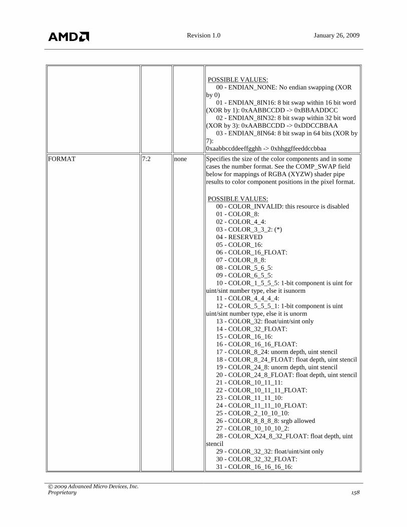
Revision 1.0 January 26, 2009
© 2009 Advanced Micro Devices, Inc. Proprietary 158
POSSIBLE VALUES:
00 - ENDIAN_NONE: No endian swapping (XOR
by 0)
01 - ENDIAN_8IN16: 8 bit swap within 16 bit word
(XOR by 1): 0xAABBCCDD -> 0xBBAADDCC
02 - ENDIAN_8IN32: 8 bit swap within 32 bit word
(XOR by 3): 0xAABBCCDD -> 0xDDCCBBAA
03 - ENDIAN_8IN64: 8 bit swap in 64 bits (XOR by
7):
0xaabbccddeeffgghh -> 0xhhggffeeddccbbaa
FORMAT 7:2 none Specifies the size of the color components and in some
cases the number format. See the COMP_SWAP field
below for mappings of RGBA (XYZW) shader pipe
results to color component positions in the pixel format.
POSSIBLE VALUES:
00 - COLOR_INVALID: this resource is disabled
01 - COLOR_8:
02 - COLOR_4_4:
03 - COLOR_3_3_2: (*)
04 - RESERVED
05 - COLOR_16:
06 - COLOR_16_FLOAT:
07 - COLOR_8_8:
08 - COLOR_5_6_5:
09 - COLOR_6_5_5:
10 - COLOR_1_5_5_5: 1-bit component is uint for
uint/sint number type, else it isunorm
11 - COLOR_4_4_4_4:
12 - COLOR_5_5_5_1: 1-bit component is uint
uint/sint number type, else it is unorm
13 - COLOR_32: float/uint/sint only
14 - COLOR_32_FLOAT:
15 - COLOR_16_16:
16 - COLOR_16_16_FLOAT:
17 - COLOR_8_24: unorm depth, uint stencil
18 - COLOR_8_24_FLOAT: float depth, uint stencil
19 - COLOR_24_8: unorm depth, uint stencil
20 - COLOR_24_8_FLOAT: float depth, uint stencil
21 - COLOR_10_11_11:
22 - COLOR_10_11_11_FLOAT:
23 - COLOR_11_11_10:
24 - COLOR_11_11_10_FLOAT:
25 - COLOR_2_10_10_10:
26 - COLOR_8_8_8_8: srgb allowed
27 - COLOR_10_10_10_2:
28 - COLOR_X24_8_32_FLOAT: float depth, uint
stencil
29 - COLOR_32_32: float/uint/sint only
30 - COLOR_32_32_FLOAT:
31 - COLOR_16_16_16_16:

Revision 1.0 January 26, 2009
© 2009 Advanced Micro Devices, Inc. Proprietary 159
32 - COLOR_16_16_16_16_FLOAT:
33 - RESERVED
34 - COLOR_32_32_32_32: float/uint/sint only
35 - COLOR_32_32_32_32_FLOAT:
ARRAY_MODE 11:8 none Specifies the tiling format of this render target array.
POSSIBLE VALUES:
00 - ARRAY_LINEAR_GENERAL: Unaligned
linear array
01 - ARRAY_LINEAR_ALIGNED: Aligned linear
array
04 - ARRAY_2D_TILED_THIN1: Uses 8x8x1
macro-tiles
NUMBER_TYPE 14:12 none Specifies the numeric type of the color components. This
field is ignored if FORMAT specifies a number type
(e.g. float or gamma).
POSSIBLE VALUES:
00 - NUMBER_UNORM: unsigned repeating
fraction (urf):
range [0..1], scale factor (2^n)-1
01 - NUMBER_SNORM: Microsoft-style signed rf:
range [-1..1], scale factor (2^(n-1))-1
02 - NUMBER_USCALED: unsigned integer,
converted to
float in shader: range [0..(2^n)-1]
03 - NUMBER_SSCALED: signed integer,
converted to
float in shader: range [-2^(n-1)..2^(n-1)-1]
04 - NUMBER_UINT: zero-extended bit field, int in
shader:
not blendable or filterable
05 - NUMBER_SINT: sign-extended bit field, int in
shader:
not blendable or filterable
06 - NUMBER_SRGB: gamma corrected, range
[0..1]
(only suported for 8-bit components
(always rounds color channels)
07 - NUMBER_FLOAT: floating point, depends on
component size:
32-bit: IEEE float, SE8M23, bias 127, range (-
2^129..2^129)
24-bit: Depth float, E4M20, bias 15, range [0..1]
16-bit: Short float SE5M10, bias 15, range (-2^17..2^17)
11-bit: Packed float, E5M6 bias 15, range [0..2^17)
10-bit: Packed float, E5M5 bias 15, range [0..2^17)
all other component sizes are treated as UINT
READ_SIZE 15 none Specifies the preferred read size: larger reads are more
efficient for PCIE accesses, for example.

Revision 1.0 January 26, 2009
© 2009 Advanced Micro Devices, Inc. Proprietary 160
POSSIBLE VALUES:
00 - READ_256_BITS
01 - READ_512_BITS
COMP_SWAP 17:16 none Specifies how to map the red, green, blue, and alpha
components from the shader to the components in the
frame buffer pixel format. There are four choices for
each number of components. With one component, the
four modes select any one component. With 2-4
components, SWAP_STD selects the low order shader
components in little-endian order; SWAP_ALT selects
an alternate order (for 4 compoents) or inclusion of alpha
(for 2 or 3 components); and the other two reverse the
component orders for use on big-endian machines. The
following table specifies the exact component mappings:
1 comp std alt std_rev alt_rev\
----------- ------- ------- ------- -------
comp 0: red green blue alpha
2 comps std alt std_rev alt_rev
----------- ------- ------- ------- -------
comp 0: red red green alpha
comp 1: green alpha red red
3 comps std alt std_rev alt_rev
----------- ------- ------- ------- -------
comp 0: red red blue alpha
comp 1: green green green green
comp 2: blue alpha red red
4 comps std alt std_rev alt_rev
----------- ------- ------- ------- -------
comp 0: red blue alpha alpha
comp 1: green green blue red
comp 2: blue red green green
comp 3: alpha alpha red blue
POSSIBLE VALUES:
00 - SWAP_STD: standard little-endian comp order
01 - SWAP_ALT: alternate components or order
02 - SWAP_STD_REV: reverses SWAP_STD order
03 - SWAP_ALT_REV: reverses SWAP_ALT order
TILE_MODE 19:18 none Selects how and whether to use per-tile CMASK and
FMASK per-tile data with this surface.
POSSIBLE VALUES:
00 - TILE_DISABLE: do not access any per-tile data
01 - TILE_CLEAR_ENABLE: allow background
clear only
02 - TILE_FRAG_ENABLE: allow background clear
and multi-sample fragment masks

Revision 1.0 January 26, 2009
© 2009 Advanced Micro Devices, Inc. Proprietary 161
BLEND_CLAMP 20 none Specifies whether to clamp source data to the render
target range prior to blending, in addition to the post-
blend clamp. This bit must be zero for uscaled, sscaled
and float number types and when blend_bypass is set.
CLEAR_COLOR 21 none If false, use RGB=0.0 and A=1.0 (0x3f800000) to
expand fast-cleared tiles. If true, use the CB_CLEAR
register values to expand fast-cleared tiles.
BLEND_BYPASS 22 none If false, blending occurs normaly as specified in
CB_BLEND#_CONTROL. If true, blending (but not
fog) is disabled. This must be set for the 24_8 and 8_24
formats and when the number type is uint or sint. It
should also be set for number types that are required to
ignore the blend state in a specific aplication interface.
BLEND_FLOAT32 23 none If true, use 32-bit float precision for source colors, else
truncate to 12-bit mantissa precision. This applies even if
blending is disabled so that a null blend and blend
disable produce the same result. This field is ignored for
NUMBER_UINT and NUMBER_SINT. It must be one
for floating point components larger than 16-bits or non-
floating components larger than 12-bits, otherwise it
must be 0.
SIMPLE_FLOAT 24 none If false, floating point processing follows full IEEE rules
for INF, NaN, and -0. If true, 0*anything produces 0 and
no operation produces -0.
ROUND_MODE 25 none This field selects between truncating (standard for floats)
and rounding (standard for most other cases) to convert
blender results to frame buffer components. The
ROUND_BY_HALF setting can be over-riden by the
DITHER_ENABLE field in CB_COLOR_CONTROL.
POSSIBLE VALUES:
00 - ROUND_BY_HALF: add 1/2 lsb and then
truncate
01 - ROUND_TRUNCATE: truncate toward zero for
float, else toward negative
TILE_COMPACT 26 none If true, this surface is compacted to eliminate storage that
would be unused due to multi-chip supertiling. The
supertiling mode is specified in
PA_SC_MULTI_CHIP_CNTL. If this bit is set, then
MULTI_CHIP_SUPERTILE_ENABLE must be set in
PA_SC_MODE_CNTL.
SOURCE_FORMAT 27 none This field indicates the allowed format for color data
being exported from the pixel shader into the output
merge block. This field may only be set to
EXPORT_NORM if BLEND_CLAMP is enabled,
BLEND_FLOAT32 is disabled, and the render target has
only 11-bit or smaller UNORM or SNORM components.
Selecting EXPORT_NORM flushes to zero values with
exponent less than 0x70 (values less than 2^-15).

Revision 1.0 January 26, 2009
© 2009 Advanced Micro Devices, Inc. Proprietary 162
POSSIBLE VALUES:
00 - EXPORT_FULL: PS exports must use the full
32-bits per component
01 - EXPORT_NORM: PS exports may use a 16-bit
per component format that supports 11-bit or smaller
UNORM, SNORM, and SRGB
CB:CB_COLOR[0-7]_MASK · [R/W] · 32 bits · Access: 32 · GpuF0MMReg:0x28100-0x2811c
Field Name Bits Default Description
CMASK_BLOCK_MAX 11:0 none This field equals one less than the number of 128x128
blocks of color mask data per 2D slice. For R600, 4-bit
CMASK values are stored in macro-tiles that have pixel
width and height determined by computing
sqrt(Pipes*16K and rounding up (for width) or down (for
height) to the nearest power of two. The pitch for the
Cmask array is derived from PITCH_TILE_MAX,
padding to the nearest multiple of the macro tile width.
FMASK_TILE_MAX 31:12 none This field equals one less than the number of 8x8 tiles of
fragment mask data per 2D slice. For R600, FMASK
values are stored in macro-tiles that have pixel width and
height determined ... TBD. The pitch for the Fmask array
is derived from PITCH_TILE_MAX, padding to the
nearest multiple of the macro tile width.
CB:CB_COLOR[0-7]_SIZE · [R/W] · 32 bits · Access: 32 · GpuF0MMReg:0x28060-0x2807c
Field Name Bits Default Description
PITCH_TILE_MAX 9:0 none Define Pitch as the number of data elements per scanline.
This field equals (Pitch/8) - 1, which equals the
maximum 8x8 tile number allowed in the X dimension
for the surface.
Allowed values for Pitch depend on ARRAY_MODE,
ElemBytes (the number of bytes per data element: 1 to
16), and Samples (the number of multi-samples per
pixel: 1, 2, 4, or 8). It also depends on two configuration
parameters that are the same for all resources:
GroupBytes (the bytes per memory interleave group: 256
or 512), and Banks (the number of DDRAM banks: 4 or
8).
Linear: Pitch*ElemBytes is a multiple of GroupBytes
and Pitch is a multiple of 64
1D tiled: Pitch*8*ElemBytes*Samples is a multiple of
GroupBytes and Pitch is a multiple of 8
2D/3D tiled: Pitch*8*ElemBytes*Samples/Banks is
multiple
of GroupBytes and Pitch is a multiple of 8*Banks/Factor

Revision 1.0 January 26, 2009
© 2009 Advanced Micro Devices, Inc. Proprietary 163
where Factor is 1, 2, or 4 for THIN1/THIN2/THIN4
2B/3B tiled: also padded to bank swap boundaries,
which are determined from GB_TILING_CONFIG fields
In addition to these constraints
SLICE_TILE_MAX 29:10 none Define SliceTiles as (Pitch*Height/64). This field equals
SliceTiles-1, and is the maximum allowed 8x8 or 64x1
tile number within an (x,y) slice of a 2D or 3D surface.
The following constraints apply to allowable heights and
z-depths for resources (see the ARRAY_MODE field):
All cases: Height is in the range [1..8192].
1D tiling: Height is a multiple of 8.
2D THIN1 tiling: Height is a multiple of 8*Pipes
2D THIN2 tiling: Height is a multiple of 16*Pipes
(and pitch is a multiple of 4*Banks)
2D THIN4 tiling: Height is a multiple of 32*Pipes
(and pitch is a multiple of 2*Banks)
2D THICK tiling: Height is a multiple of 8*Pipes
and z-depth is a multiple of 4
Note: Pitch, height and Z-depth must be powers of 2 for
mipmap chains (other than the base map).
CB:CB_COLOR[0-7]_TILE · [R/W] · 32 bits · Access: 32 · GpuF0MMReg:0x280c0-0x280dc
Field Name Bits Default Description
BASE_256B 31:0 none This value times 256 is the byte address of the start of
the CMASK per-tile data, if any, in device address space.
In other words, this field is the high 32-bits of an up to
40-bit virtual device address.
CB:CB_COLOR[0-7]_VIEW · [R/W] · 32 bits · Access: 32 · GpuF0MMReg:0x28080-0x2809c
DESCRIPTION: Selects slice index range for render target 0.
Field Name Bits Default Description
SLICE_START 10:0 none For ARRAY_LINEAR_GENERAL the low 8-bits
together with BASE_256B specify a 40-bit starting
addressess (must be element-aligned).
Else this specifies the starting slice number for this view:
this field is added to the RenderTargetArrayIndex to
compute the slice to render.
SLICE_MAX 23:13 none Specifies the maximum allowed Z slice index for this
resource, which is one less than the total number of
slices. Clamp Z slice to SLICE_START if this value is
exceeded (clamp to zero for
ARRAY_LINEAR_GENERAL).
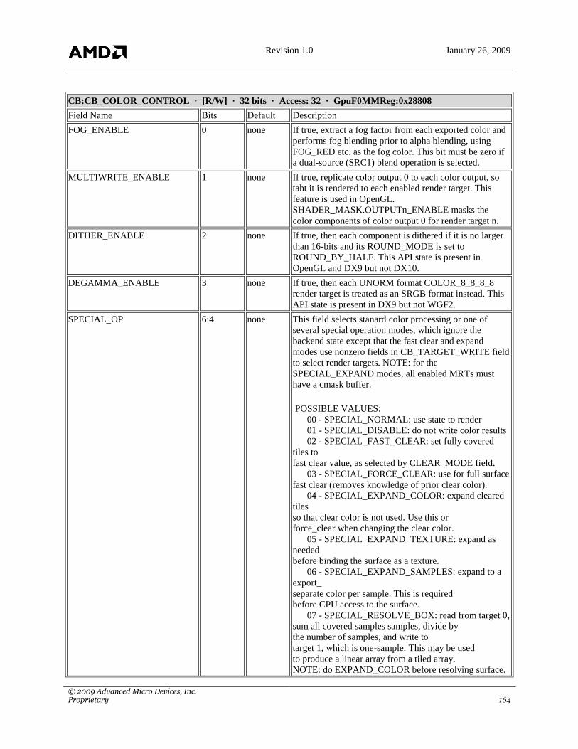
Revision 1.0 January 26, 2009
© 2009 Advanced Micro Devices, Inc. Proprietary 164
CB:CB_COLOR_CONTROL · [R/W] · 32 bits · Access: 32 · GpuF0MMReg:0x28808
Field Name Bits Default Description
FOG_ENABLE 0 none If true, extract a fog factor from each exported color and
performs fog blending prior to alpha blending, using
FOG_RED etc. as the fog color. This bit must be zero if
a dual-source (SRC1) blend operation is selected.
MULTIWRITE_ENABLE 1 none If true, replicate color output 0 to each color output, so
taht it is rendered to each enabled render target. This
feature is used in OpenGL.
SHADER_MASK.OUTPUTn_ENABLE masks the
color components of color output 0 for render target n.
DITHER_ENABLE 2 none If true, then each component is dithered if it is no larger
than 16-bits and its ROUND_MODE is set to
ROUND_BY_HALF. This API state is present in
OpenGL and DX9 but not DX10.
DEGAMMA_ENABLE 3 none If true, then each UNORM format COLOR_8_8_8_8
render target is treated as an SRGB format instead. This
API state is present in DX9 but not WGF2.
SPECIAL_OP 6:4 none This field selects stanard color processing or one of
several special operation modes, which ignore the
backend state except that the fast clear and expand
modes use nonzero fields in CB_TARGET_WRITE field
to select render targets. NOTE: for the
SPECIAL_EXPAND modes, all enabled MRTs must
have a cmask buffer.
POSSIBLE VALUES:
00 - SPECIAL_NORMAL: use state to render
01 - SPECIAL_DISABLE: do not write color results
02 - SPECIAL_FAST_CLEAR: set fully covered
tiles to
fast clear value, as selected by CLEAR_MODE field.
03 - SPECIAL_FORCE_CLEAR: use for full surface
fast clear (removes knowledge of prior clear color).
04 - SPECIAL_EXPAND_COLOR: expand cleared
tiles
so that clear color is not used. Use this or
force_clear when changing the clear color.
05 - SPECIAL_EXPAND_TEXTURE: expand as
needed
before binding the surface as a texture.
06 - SPECIAL_EXPAND_SAMPLES: expand to a
export_
separate color per sample. This is required
before CPU access to the surface.
07 - SPECIAL_RESOLVE_BOX: read from target 0,
sum all covered samples samples, divide by
the number of samples, and write to
target 1, which is one-sample. This may be used
to produce a linear array from a tiled array.
NOTE: do EXPAND_COLOR before resolving surface.

Revision 1.0 January 26, 2009
© 2009 Advanced Micro Devices, Inc. Proprietary 165
PER_MRT_BLEND 7 none If false, use CB_BLEND_CONTROL for all blend
functions. If true, use CB_BLEND#_CONTROL for the
blend function for render target # (if blending is
enabled).
TARGET_BLEND_ENABLE 15:8 none Each bit enables blending for the corresponding render
target if it is 1, else disables blending for that render
target if it is 0. This field must be 0xcc (source) if
BLEND_FLOAT32 is set for any enabled render target.
ROP3 23:16 none This field supports the 28 boolean ops that combine
either source and dest or brush and dest, with brush
provided by the shader in place of source. ROP3 codes
that use both src and brush are emulated in software.
Allowed ROP3 codes have either the form pqrspqrs (for
source/dest ops) or pqpqrsrs (for brush/dest ops). The
code 0xCC (11001100) copies the source to the
destination, which disables the ROP function.
CB:CB_FOG_BLUE · [R/W] · 32 bits · Access: 32 · GpuF0MMReg:0x2842c
Field Name Bits Default Description
FOG_BLUE 31:0 none Blue component of fog color, specified in IEEE floating
point.
CB:CB_FOG_GREEN · [R/W] · 32 bits · Access: 32 · GpuF0MMReg:0x28428
Field Name Bits Default Description
FOG_GREEN 31:0 none Green component of fog color, specified in IEEE floating
point.
CB:CB_FOG_RED · [R/W] · 32 bits · Access: 32 · GpuF0MMReg:0x28424
Field Name Bits Default Description
FOG_RED 31:0 none Red component of fog color, specified in IEEE floating
point.
CB:CB_SHADER_MASK · [R/W] · 32 bits · Access: 32 · GpuF0MMReg:0x2823c
DESCRIPTION: Contains color component mask fields for the colors output by the shader. Outputs 1-7 are
defined equivalently to output 0.
Field Name Bits Default Description
OUTPUT0_ENABLE 3:0 none If zero, this field disables writes to render target 0, else it
specifies which components are enabled in the shader.
The low order bit corresponds to the red channel. A one
bit bit passes the shader output component value to the
color block. A zero bit replaces the component with the
default value: 0.0 for RGB or 1.0 for alpha.
OUTPUT1_ENABLE 7:4 none
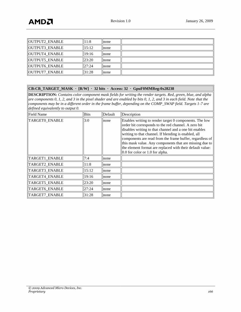
Revision 1.0 January 26, 2009
© 2009 Advanced Micro Devices, Inc. Proprietary 166
OUTPUT2_ENABLE 11:8 none
OUTPUT3_ENABLE 15:12 none
OUTPUT4_ENABLE 19:16 none
OUTPUT5_ENABLE 23:20 none
OUTPUT6_ENABLE 27:24 none
OUTPUT7_ENABLE 31:28 none
CB:CB_TARGET_MASK · [R/W] · 32 bits · Access: 32 · GpuF0MMReg:0x28238
DESCRIPTION: Contains color component mask fields for writing the render targets. Red, green, blue, and alpha
are components 0, 1, 2, and 3 in the pixel shader and are enabled by bits 0, 1, 2, and 3 in each field. Note that the
components may be in a different order in the frame buffer, depending on the COMP_SWAP field. Targets 1-7 are
defined equivalently to output 0.
Field Name Bits Default Description
TARGET0_ENABLE 3:0 none Enables writing to render target 0 components. The low
order bit corresponds to the red channel. A zero bit
disables writing to that channel and a one bit enables
writing to that channel. If blending is enabled, all
components are read from the frame buffer, regardless of
this mask value. Any components that are missing due to
the element format are replaced with their default value:
0.0 for color or 1.0 for alpha.
TARGET1_ENABLE 7:4 none
TARGET2_ENABLE 11:8 none
TARGET3_ENABLE 15:12 none
TARGET4_ENABLE 19:16 none
TARGET5_ENABLE 23:20 none
TARGET6_ENABLE 27:24 none
TARGET7_ENABLE 31:28 none