rad hard egan® 40v, 30a, 6mΩ surface mount (fsmd...
TRANSCRIPT

FBG04N30B Rev 1.0 1 www.freebirdsemi.com Mar 28 , 2017
FBG04N30B Rad Hard eGaN® 40V, 30A, 6mΩ Surface Mount (FSMD-B)
Features Low RDS(ON) Ultra-low QG For High Efficiency Logic Level Light Weight – 0.135 grams New Compact Hermetic Package Source Sense Pin Total Dose
- Rated to 300kRad Single Event
- SEE immunity for LET of 83.7 MeV/mg/cm2 With VDS up to 100% of rated Breakdown
Low Dose Rate at 100 mRad/sec - Maintains Pre-Rad specification
Neutron - Maintains Pre-Rad specification for
up to 1 x 10¹³ Neutrons/cm2
Description Freebird Semiconductor FSMD-B series of eGaN® power switching HEMTs have been specifically designed for critical applications in the high reliability or commercial satellite space environments. These devices have exceptionally high electron mobility and a low temperature coefficient resulting in very low RDS(ON)
values. The lateral structure of the die provides for very low gate charge (QG) and extremely fast switching times. These features enable faster power supply switching frequencies resulting in higher power densities, higher efficiencies and more compact packaging. Application
Commercial Satellite EPS & Avionics Deep Space Probes High Speed Rad Hard DC-DC Conversion Rad Hard Motor Controllers
Absolute Maximum Rating TC =25 oC unless otherwise noted
Symbol Parameter-Conditions Value Units VDS Drain to Source Voltage (Note 1) 40 V ID Continuous Drain Current ID @ VGS=4.5V, TC= 25 oC, RθJA<35 oC/W 30
A IDM Single-Pulse Drain Current tpulse ≤ 80µs 100 VGS Gate to Source Voltage (Note 2) +6 / -4 V TJ, TSTG Operating and Storage Junction Temperature Range -55 to +150 oC Tsol Package Mounting Surface Temperature 260 oC
ESD ESD class level 1A
Thermal Characteristics
Symbol Parameter-Conditions Value Units RθJA Thermal Resistance Junction to Ambient (Note 3) 35 oC/W RθJC Thermal Resistance Junction to Case 2.12
I/O Pin Assignment (Bottom View)
Pin Symbol Description Visual Outline Physical device 1 G Gate
2 D Drain 3 S Source 4 SS Source Sense
Electrical Characteristics TC =25 oC unless otherwise noted. Typical (TYP) values are for reference only.

FBG04N30B
©2017 Freebird Semiconductor Corporation Page 2 of 14 freebirdsemi.com
PARAMETER SYMBOL TEST CONDITIONS MIN TYP MAX UNITS
Maximum Drain to Source Voltage VDSMAX VGS= 0V - - 40 V
Drain to Source Leakage IDSS VDS = 40V VGS = 0V
Tc= 25 oC - 26 400 µA
Tc= 125 oC - 1000 Gate to Source Forward Leakage IGSS VGS = 5V Tc= 25 oC - 0.1 7 mA
Gate to Source Reverse Leakage IGSS VGS = -4V Tc= 25 oC -50 -400 µA Gate to Source Threshold Voltage VGS(th) VDS = VGS, ID = 9mA Tc= 25 oC 0.8 1.0 2.5 V
Gate to Source Threshold Voltage Temperature Coefficient ∆VGS(th) /∆T VDS = VGS, ID = 5mA -55 oC < TA < 150 oC - |1.5| - mV/ºC
Drain to Source Resistance (Note 4) RDS(ON) ID = 30A, VGS = 3.5V Tc= 25 oC - 4.0
mΩ ID = 30A, VGS = 5.0V Tc= 25 oC - 3.5 6
Source to Drain Forward Voltage (Note 5) VSD IS = 5A, VG = 0V Tc= 25 oC 1.70 V
Dynamic Characteristics TC =25 oC unless otherwise noted. Typical (TYP) values are for reference only.
PARAMETER SYMBOL TEST CONDITIONS MIN TYP MAX UNITS
Input Capacitance CISS f = 1MHz, VDS = 20V, VGS=0V (Note 6)
1100 1300 pF Output Capacitance COSS 650 800 pF Reverse transfer Capacitance CRSS 30 40 pF Gate Resistance RG f = 1MHz, VDS = VGS =0 V 1.1 Ω
Total Gate Charge (Note 7) QG ID =15 A, VGS = 5V, VDS =20V 8.9
nC ID =30 A, VGS = 5V, VDS =20V 8.9 11.4
Gate to Drain Charge (Note 7) QGD ID =15 A, VGS = 5V, VDS =20V 1.8
nC ID =30 A, VGS = 5V, VDS =20V 2.1 3.0
Gate to Source Charge (Note 7) QGS ID =15 A, VGS = 5V, VDS =20V 1.9
nC ID =30 A, VGS = 5V, VDS =20V 2.3 3.1
Output Charge (Note 8) QOSS VGS = 0V, VDS =20V 22 26 nC Source to Drain Recovery Charge QRR ID =30 A, VDS =20V <1 nC
FBG04N30B
©2017 Freebird Semiconductor Corporation Page 3 of 14 freebirdsemi.com
Radiation Characteristics
Freebird Semiconductor eGaN® HEMTs are tested according to MIL-STD-750 Method 1019 for total ionizing dose validation. Every manufacturing lot is tested for total ionizing dose of Gamma radiation with an in-situ bias for (i) VGS = 5V, (ii) VDS=VGS=0V and (iii) VDS=80% BVDSS.
Electrical Characteristics up to 300 kRads TC =25 oC unless otherwise noted. Typical (TYP) values are for reference only.
PARAMETER SYMBOL TEST CONDITIONS MIN TYP MAX UNITS
Maximum Drain to Source Voltage VDSMAX VGS= 0V - - 40 V Gate to Source Threshold Voltage VGS(th) VDS = VGS, ID = 9mA 0.8 1.0 2.5 V Drain to Source Leakage IDSS VDS = 40V , VGS = 0V - 26 400 µA Gate to Source Forward Leakage IGSS VGS = 5V - 0.1 7 mA Gate to Source Reverse Leakage IGSS VGS = -4V - -50 -400 µA Drain to Source Resistance (Note 4) RDS(ON) ID = 30A, VGS = 5.0V - 3.5 6.0 mΩ
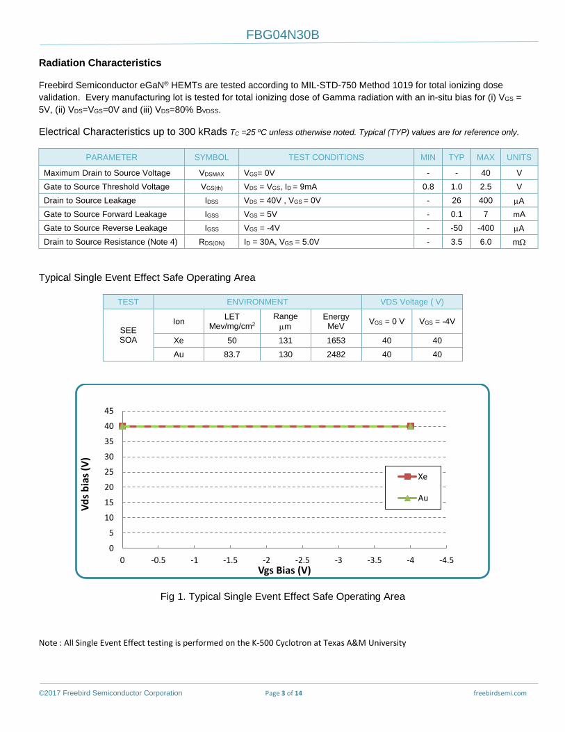
Typical Single Event Effect Safe Operating Area
TEST ENVIRONMENT VDS Voltage ( V)
SEE SOA
Ion LET Mev/mg/cm2
Range µm
Energy MeV VGS = 0 V VGS = -4V
Xe 50 131 1653 40 40 Au 83.7 130 2482 40 40
Fig 1. Typical Single Event Effect Safe Operating Area
Note : All Single Event Effect testing is performed on the K-500 Cyclotron at Texas A&M University
0
5
10
15
20
25
30
35
40
45
-4.5-4-3.5-3-2.5-2-1.5-1-0.50
Vds b
ias (
V)
Vgs Bias (V)
Xe
Au
FBG04N30B
©2017 Freebird Semiconductor Corporation Page 4 of 14 freebirdsemi.com
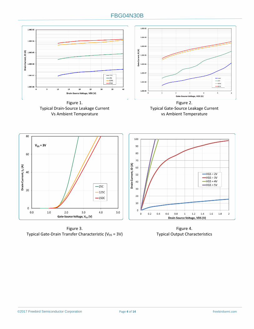
Figure 1. Figure 2. Typical Drain-Source Leakage Current Typical Gate-Source Leakage Current Vs Ambient Temperature vs Ambient Temperature
Figure 3. Figure 4. Typical Gate-Drain Transfer Characteristic (VDS = 3V) Typical Output Characteristics

FBG04N30B
©2017 Freebird Semiconductor Corporation Page 5 of 14 freebirdsemi.com
Figure 5. Figure 6. Typical Drain-Source ON Resistance Typical Drain-Source ON Resistance vs Gate-Source Voltage vs Ambient Temperature vs Gate-Source Voltage vs Drain Current
Figure 7. Figure 8. Typical Source-Drain Voltage vs Temperature Typical Normalized Drain-Source ON Resistance vs Ambient Temperature
ID = 15A

FBG04N30B
©2017 Freebird Semiconductor Corporation Page 6 of 14 freebirdsemi.com
Figure 9. Figure 10. Typical Inter-Electrode Capacitance Typical Gate Charge vs Drain Current vs Drain-Source Voltage
Figure 10. Safe Operating Area
FBG04N30B
©2017 Freebird Semiconductor Corporation Page 7 of 14 freebirdsemi.com
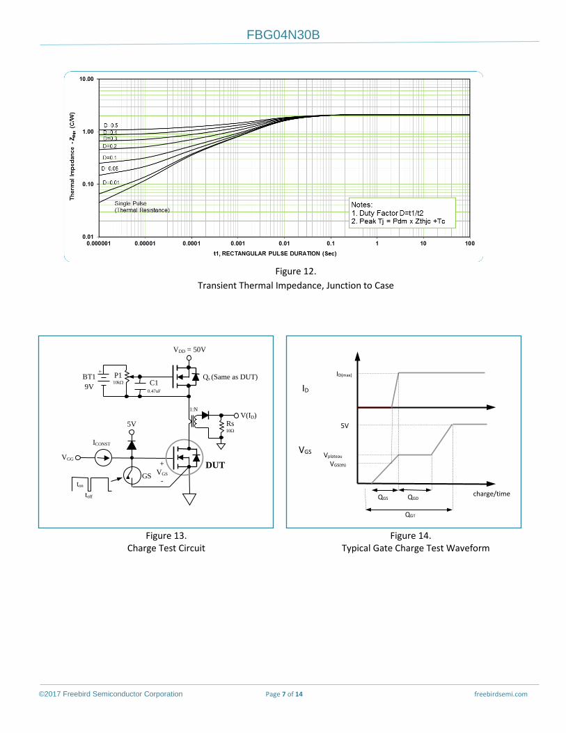
Figure 12.
Transient Thermal Impedance, Junction to Case
Figure 13. Figure 14. Charge Test Circuit Typical Gate Charge Test Waveform
VGG
5V
+ VGS
- ton toff
ICONST
VDD = 50V
DUT GS
BT1 9V C1
0.47uF
P1 10kΩ
+
1:N
Rs 10Ω
V(ID)
Qs (Same as DUT) ID
5V
Vplateau VGS(th)
VGS
QGS QGD charge/time
QGT
ID(max)

FBG04N30B
©2017 Freebird Semiconductor Corporation Page 8 of 14 freebirdsemi.com
PACKAGE OUTLINE AND DIMENSIONS
Symbol Inches Millimeters
Note Min Max Min Max
A 0.027 0.037 0.686 0.940 B 0.073 0.083 1.854 2.108 C 0.035 0.045 0.889 1.143 D 0.142 0.152 3.607 3.861 F 0.025 0.035 0.635 0.889 G 0.085 0.095 2.159 2.413 H 0.134 0.144 3.404 3.658 J 0.045 0.055 1.143 1.397 K 0.076 0.086 1.930 2.184 L 0.215 0.225 5.461 5.715 M 0.058 0.068 1.473 1.727 N 0.016 0.026 0.406 0.660 P 0.145 0.155 3.683 3.937
FSMD-B FOOTPRINT FOR PRINTED CIRCUIT BOARD DESIGN
Symbol Inches Millimeters
Note Min Max Min Max
A 0.063 0.073 1.600 1.854
B 0.010 0.020 0.254 0.508
C 0.063 0.073 1.600 1.854
D 0.037 0.047 0.940 1.194
E 0.025 0.035 0.635 0.889
F 0.144 0.154 3.658 3.912
G 0.055 0.065 1.397 1.651
H 0.025 0.035 0.635 0.889
J 0.055 0.065 1.397 1.651
FBG04N30B
©2017 Freebird Semiconductor Corporation Page 9 of 14 freebirdsemi.com
NOTE: Note 1. NEVER exceed the absolute maximum VDS of the device otherwise permanent damage/destruction may result. Note 2. NEVER exceed the absolute maximum VGS of the device otherwise permanent damage/destruction may result. We recommend use at no
greater than +5V as the HEMT is fully conducting at this point. Note 3. RθJA measured with FSMD-B package mounted to double-sided PCB, 0.063” thickness with 1.0 square inches of copper area on the top
(mounting side) and a flood etch (3 square inches) on the bottom side. Note 4. Measured using four wire (Kelvin) sensing and pulse measurement techniques. Measurement pulse width is 80µs and duty cycle is 1%,
maximum. Note 5. Operation of the device in the third quadrant region is not recommended. Note 6. Ciss = CGS + CGD with CDS shorted. Coss = CDS + CGD. Crss = CGD. Note 7. The gate charge parameters are measured using the circuit shown in Figure 11. Qs and associated components BT1, P1 and C1 form a high
speed current source that serves as the test load for the DUT. A constant gate current (Iconst) of 1.5-3mA is provided to the Gate of the DUT during the time that the ground switch (GS) is OFF (toff). The DUT is switched ON and OFF using ground-sensed switch GS. The gate current is adjusted to yield the desired charge per unit time (Iconst * time per division) on the measuring oscilloscope. The GS pulse drive ON time (ton)is adjusted for the desired observability of the gate-source voltage (VGS) waveform. The maximum duty cycle of the ground switch (toff/ton) should be set to 1% maximum. Please note that all gate-related signals are referenced to the “Source Sense” pin on the package. At all times during the measurement, the maximum gate-source voltage is clamped to 5Vdc.
Note 8. Guaranteed by design/device construction. Not tested.
FBG04N30B
©2017 Freebird Semiconductor Corporation Page 10 of 14 freebirdsemi.com
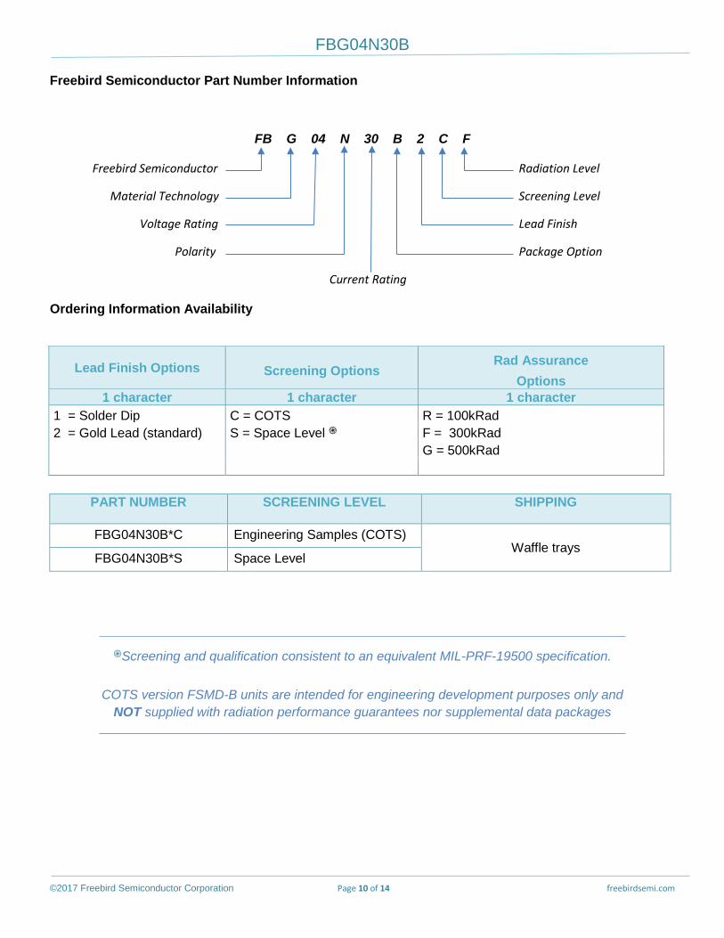
Freebird Semiconductor Part Number Information
FB G 04 N 30 B 2 C F
Freebird Semiconductor Radiation Level
Material Technology Screening Level
Voltage Rating Lead Finish
Polarity Package Option
Current Rating
Ordering Information Availability
Screening and qualification consistent to an equivalent MIL-PRF-19500 specification.
COTS version FSMD-B units are intended for engineering development purposes only and NOT supplied with radiation performance guarantees nor supplemental data packages
Lead Finish Options Screening OptionsRad Assurance
Options1 character 1 character 1 character
1 = Solder Dip C = COTS R = 100kRad 2 = Gold Lead (standard) S = Space Level F = 300kRad G = 500kRad
PART NUMBER SCREENING LEVEL SHIPPING
FBG04N30B*C Engineering Samples (COTS) Waffle trays
FBG04N30B*S Space Level

FBG04N30B
©2017 Freebird Semiconductor Corporation Page 11 of 14 freebirdsemi.com
Freebird Semiconductor Product Marking Information
XXXX – serialization number when required
Part number & package information plus:
L lead finish option S screening level H radiation level
Company Identifier (FBS), date code and CAGE code:
YY Last two digits of the current year WW Week number according to ISO 8601 7FW34 CAGE code
ESD rating of the device located directly over the Gate pin

FBG04N30B
©2017 Freebird Semiconductor Corporation Page 12 of 14 freebirdsemi.com
Data Package Order Detail Consistent to MIL-PRF-19500 general specification
“SPACE Screen”
1. FBG04N30B*S - STANDARD DATA PACKAGE
A. Certificate of Compliance
B. Serialization Records
C. Assembly Flow Chart
D. Preconditioning - Attributes Data Sheet - HTRB - Hi Temp Gate Stress Post Reverse Bias Data and Delta Data
- HTRB - Hi Temp Drain Stress Post Reverse Bias Delta Data
E. Group A - Attributes Data Sheet
F. Group B - Attributes Data Sheet
G. Group C - Attributes Data Sheet
H. Group D - Attributes Data Sheet
2. FBG04N30B*S - OPTIONAL DATA PACKAGE A. Certificate of Compliance
B. Serialization Records
C. Assembly Flow Chart
D. SEM Photos and Report
E. Preconditioning - Attributes Data Sheet - HTRB - Hi Temp Gate Stress Post Reverse Bias Data and Delta
Data - HTRB - Hi Temp Drain Stress Post Reverse Bias Delta Data
- X-Ray and X-Ray Report
F. Group A - Attributes Data Sheet - Subgroups A2, A3, A4 and A7 Data
G. Group B - Attributes Data Sheet - Subgroups B1, B2, B4, B5 and B6 Data
H. Group C - Attributes Data Sheet - Subgroups C1, C2, C3 and C6 Data
I. Group D - Attributes Data Sheet - Pre and Post Radiation Data

FBG04N30B Rev 1.0 1 www.freebirdsemi.com Mar 28 , 2017
FBG04N30B Rad Hard eGaN® 40V, 30A, 6mΩ Surface Mount (FSMD-B)
Disclaimers
ALL PRODUCT, PRODUCT SPECIFICATIONS AND DATA ARE SUBJECT TO CHANGE WITHOUT NOTICE TO IMPROVE RELIABILITY, FUNCTION OR DESIGN OR OTHERWISE. Freebird Semiconductor Corporation, its affiliates, agents, employees, and all persons acting on its or their behalf (collectively, “Freebird”), disclaim any and all liability for any errors, inaccuracies or incompleteness contained in any datasheet or in any other disclosure relating to any product. Freebird makes no warranty, representation or guarantee regarding the suitability of the products for any particular purpose. To the maximum extent permitted by applicable law, Freebird disclaims (i) any and all liability arising out of the application or use of any product, (ii) any and all liability, including without limitation special, consequential or incidental damages, and (iii) any and all implied warranties, including warranties of fitness for particular purpose, non-infringement and merchantability. Statements regarding the suitability of products for certain types of applications are based on Freebird market knowledge of typical requirements that are often placed on similar technologies in generic applications. Product specifications do not expand or otherwise modify Freebird terms and conditions of purchase, including but not limited to the warranty expressed therein. Except as expressly indicated in writing, Freebird products are not designed for use in medical, life-saving, or life-sustaining applications or for any other application in which the failure of the Freebird product could result in personal injury or death. Customers using Freebird products not expressly indicated for use in such applications do so at their own risk. Please contact authorized Freebird personnel to obtain written terms and conditions regarding products designed for such applications. No license, express or implied, by estoppel or otherwise, to any intellectual property rights is granted by this document or by any conduct of Freebird. Product names and markings noted herein may be trademarks of their respective owners.
Export Administration Regulations (EAR)
The products described in this datasheet could be subjected to the Export Administration Regulations (EAR). They may require an approved export license prior to export from the United States. An export includes release of product or disclosure of technology to a foreign national inside or outside the United States.
International Traffic in Arms Regulations (ITAR)
The products described in this datasheet could be subjected to the International in Arms Regulations (ITAR). They require an approved export license prior to export from the United States. An export includes release of product or disclosure of technology to a foreign national inside or outside the United States.
Patents
Freebird Semiconductor holds numerous U.S patent. Any that apply to the product(s) listed in this document are identified by markings on the product(s) or on internal components of the product(s) in accordance with U.S Patent laws eGaN is a registered trademark of Efficient Power Conversion Corporation, Inc. Data and specification subject to change without notice.
FBG04N30B
©2017 Freebird Semiconductor Corporation Page 14 of 14 freebirdsemi.com
Revision
Datasheet Revision Product Status REV P Proposal/development REV Q Characterization and Qualification REV # Production Released
Contact Freebird Semiconductor Corporation for further information and to order: Email : [email protected]
Phone: +1 978 208 1334 Website: www.freebirdsemi.com Address: 17 Parkridge Road
Unit # E Haverhill, MA 01835 USA
Freebird Semiconductor Corporation has been assessed and registered by Intertek as conforming to the requirements of AS9100C and ISO 9001:2008 quality management system which is applicable to the design and manufacture of high reliability semiconductors devices and circuits. The assessment was performed in accordance with the requirements of AS9104/1:2012-01. Intertek is accredited under the Aerospace Management Program and IAQG ICOP scheme.