r8c/22, r8c/23 group hardware manual - digi-key sheets/renesas/rej09b0251... · all information...
TRANSCRIPT

www.renesas.com
All information contained in these materials, including products and product specifications,represents information on the product at the time of publication and is subject to change byRenesas Technology Corp. without notice. Please review the latest information publishedby Renesas Technology Corp. through various means, including the Renesas TechnologyCorp. website (http://www.renesas.com).
REJ09B0251-0200
16 R8C/22 Group, R8C/23 GroupHardware Manual
RENESAS MCUR8C FAMILY / R8C/2x SERIES
Rev.2.00Revision Date: Aug 20, 2008

1. This document is provided for reference purposes only so that Renesas customers may select the appropriate Renesas products for their use. Renesas neither makes warranties or representations with respect to the accuracy or completeness of the information contained in this document nor grants any license to any intellectual property rights or any other rights of Renesas or any third party with respect to the information in this document. 2. Renesas shall have no liability for damages or infringement of any intellectual property or other rights arising out of the use of any information in this document, including, but not limited to, product data, diagrams, charts, programs, algorithms, and application circuit examples.3. You should not use the products or the technology described in this document for the purpose of military applications such as the development of weapons of mass destruction or for the purpose of any other military use. When exporting the products or technology described herein, you should follow the applicable export control laws and regulations, and procedures required by such laws and regulations.4. All information included in this document such as product data, diagrams, charts, programs, algorithms, and application circuit examples, is current as of the date this document is issued. Such information, however, is subject to change without any prior notice. Before purchasing or using any Renesas products listed in this document, please confirm the latest product information with a Renesas sales office. Also, please pay regular and careful attention to additional and different information to be disclosed by Renesas such as that disclosed through our website. (http://www.renesas.com )5. Renesas has used reasonable care in compiling the information included in this document, but Renesas assumes no liability whatsoever for any damages incurred as a result of errors or omissions in the information included in this document.6. When using or otherwise relying on the information in this document, you should evaluate the information in light of the total system before deciding about the applicability of such information to the intended application. Renesas makes no representations, warranties or guaranties regarding the suitability of its products for any particular application and specifically disclaims any liability arising out of the application and use of the information in this document or Renesas products. 7. With the exception of products specified by Renesas as suitable for automobile applications, Renesas products are not designed, manufactured or tested for applications or otherwise in systems the failure or malfunction of which may cause a direct threat to human life or create a risk of human injury or which require especially high quality and reliability such as safety systems, or equipment or systems for transportation and traffic, healthcare, combustion control, aerospace and aeronautics, nuclear power, or undersea communication transmission. If you are considering the use of our products for such purposes, please contact a Renesas sales office beforehand. Renesas shall have no liability for damages arising out of the uses set forth above.8. Notwithstanding the preceding paragraph, you should not use Renesas products for the purposes listed below: (1) artificial life support devices or systems (2) surgical implantations (3) healthcare intervention (e.g., excision, administration of medication, etc.) (4) any other purposes that pose a direct threat to human life Renesas shall have no liability for damages arising out of the uses set forth in the above and purchasers who elect to use Renesas products in any of the foregoing applications shall indemnify and hold harmless Renesas Technology Corp., its affiliated companies and their officers, directors, and employees against any and all damages arising out of such applications. 9. You should use the products described herein within the range specified by Renesas, especially with respect to the maximum rating, operating supply voltage range, movement power voltage range, heat radiation characteristics, installation and other product characteristics. Renesas shall have no liability for malfunctions or damages arising out of the use of Renesas products beyond such specified ranges.10. Although Renesas endeavors to improve the quality and reliability of its products, IC products have specific characteristics such as the occurrence of failure at a certain rate and malfunctions under certain use conditions. Please be sure to implement safety measures to guard against the possibility of physical injury, and injury or damage caused by fire in the event of the failure of a Renesas product, such as safety design for hardware and software including but not limited to redundancy, fire control and malfunction prevention, appropriate treatment for aging degradation or any other applicable measures. Among others, since the evaluation of microcomputer software alone is very difficult, please evaluate the safety of the final products or system manufactured by you. 11. In case Renesas products listed in this document are detached from the products to which the Renesas products are attached or affixed, the risk of accident such as swallowing by infants and small children is very high. You should implement safety measures so that Renesas products may not be easily detached from your products. Renesas shall have no liability for damages arising out of such detachment.12. This document may not be reproduced or duplicated, in any form, in whole or in part, without prior written approval from Renesas. 13. Please contact a Renesas sales office if you have any questions regarding the information contained in this document, Renesas semiconductor products, or if you have any other inquiries.
Notes regarding these materials

General Precautions in the Handling of MPU/MCU Products
The following usage notes are applicable to all MPU/MCU products from Renesas. For detailed usage notes on the products covered by this manual, refer to the relevant sections of the manual. If the descriptions under General Precautions in the Handling of MPU/MCU Products and in the body of the manual differ from each other, the description in the body of the manual takes precedence.
1. Handling of Unused Pins Handle unused pins in accord with the directions given under Handling of Unused Pins in the manual. The input pins of CMOS products are generally in the high-impedance state. In operation
with an unused pin in the open-circuit state, extra electromagnetic noise is induced in the vicinity of LSI, an associated shoot-through current flows internally, and malfunctions occur due to the false recognition of the pin state as an input signal become possible. Unused pins should be handled as described under Handling of Unused Pins in the manual.
2. Processing at Power-on The state of the product is undefined at the moment when power is supplied. The states of internal circuits in the LSI are indeterminate and the states of register
settings and pins are undefined at the moment when power is supplied. In a finished product where the reset signal is applied to the external reset pin, the states of pins are not guaranteed from the moment when power is supplied until the reset process is completed. In a similar way, the states of pins in a product that is reset by an on-chip power-on reset function are not guaranteed from the moment when power is supplied until the power reaches the level at which resetting has been specified.
3. Prohibition of Access to Reserved Addresses Access to reserved addresses is prohibited. The reserved addresses are provided for the possible future expansion of functions. Do
not access these addresses; the correct operation of LSI is not guaranteed if they are accessed.
4. Clock Signals After applying a reset, only release the reset line after the operating clock signal has become stable. When switching the clock signal during program execution, wait until the target clock signal has stabilized. When the clock signal is generated with an external resonator (or from an external
oscillator) during a reset, ensure that the reset line is only released after full stabilization of the clock signal. Moreover, when switching to a clock signal produced with an external resonator (or by an external oscillator) while program execution is in progress, wait until the target clock signal is stable.
5. Differences between Products Before changing from one product to another, i.e. to one with a different part number, confirm that the change will not lead to problems. The characteristics of MPU/MCU in the same group but having different part numbers may
differ because of the differences in internal memory capacity and layout pattern. When changing to products of different part numbers, implement a system-evaluation test for each of the products.

How to Use This Manual1. Purpose and Target Readers
This manual is designed to provide the user with an understanding of the hardware functions and electricalcharacteristics of the MCU. It is intended for users designing application systems incorporating the MCU. A basicknowledge of electric circuits, logical circuits, and MCUs is necessary in order to use this manual.The manual comprises an overview of the product; descriptions of the CPU, system control functions, peripheralfunctions, and electrical characteristics; and usage notes.
Particular attention should be paid to the precautionary notes when using the manual. These notes occurwithin the body of the text, at the end of each section, and in the Usage Notes section.
The revision history summarizes the locations of revisions and additions. It does not list all revisions. Referto the text of the manual for details.
The following documents apply to the R8C/22 Group and R8C/23 Group. Make sure to refer to the latest versions ofthese documents. The newest versions of the documents listed may be obtained from the Renesas Technology Website.
Document Type Description Document Title Document No.Datasheet Hardware overview and electrical characteristics R8C/22 Group,
R8C/23 Group Datasheet
REJ03B0097
Hardware manual Hardware specifications (pin assignments, memory maps, peripheral function specifications, electrical characteristics, timing charts) and operation descriptionNote: Refer to the application notes for details on using peripheral functions.
R8C/22 Group, R8C/23 Group Hardware Manual
This hardware manual
Software manual Description of CPU instruction set R8C/Tiny Series Software Manual
REJ09B0001
Application note Information on using peripheral functions and application examplesSample programsInformation on writing programs in assembly language and C
Available from Renesas Technology Web site.
Renesas technical update
Product specifications, updates on documents, etc.

2. Notation of Numbers and SymbolsThe notation conventions for register names, bit names, numbers, and symbols used in this manual are describedbelow.
(1) Register Names, Bit Names, and Pin NamesRegisters, bits, and pins are referred to in the text by symbols. The symbol is accompanied by the word“register,” “bit,” or “pin” to distinguish the three categories.Examples the PM03 bit in the PM0 register
P3_5 pin, VCC pin
(2) Notation of NumbersThe indication “b” is appended to numeric values given in binary format. However, nothing is appended to thevalues of single bits. The indication “h” is appended to numeric values given in hexadecimal format. Nothingis appended to numeric values given in decimal format.Examples Binary: 11b
Hexadecimal: EFA0hDecimal: 1234

3. Register NotationThe symbols and terms used in register diagrams are described below.
*1Blank: Set to 0 or 1 according to the application.0: Set to 0.1: Set to 1.X: Nothing is assigned.
*2RW: Read and write.RO: Read only.WO: Write only.−: Nothing is assigned.
*3• Reserved bit
Reserved bit. Set to specified value.
*4• Nothing is assigned
Nothing is assigned to the bit. As the bit may be used for future functions, if necessary, set to 0.• Do not set to a value
Operation is not guaranteed when a value is set.• Function varies according to the operating mode.
The function of the bit varies with the peripheral function mode. Refer to the register diagram for informationon the individual modes.
XXX Register
Symbol Address After Reset XXX XXX 00h
Bit NameBit Symbol RW
b7 b6 b5 b4 b3 b2 b1 b0
XXX bits 1 0: XXX0 1: XXX1 0: Do not set.1 1: XXX
b1 b0
XXX1
XXX0
XXX4
Reserved bits
XXX5
XXX7
XXX6
Function
Nothing is assigned. If necessary, set to 0.When read, the content is undefined.
XXX bit
Function varies according to the operatingmode.
Set to 0.
0
(b3)
(b2)
RW
RW
RW
RW
WO
RW
RO
XXX bits
0: XXX1: XXX
*1
*2
*3
*4
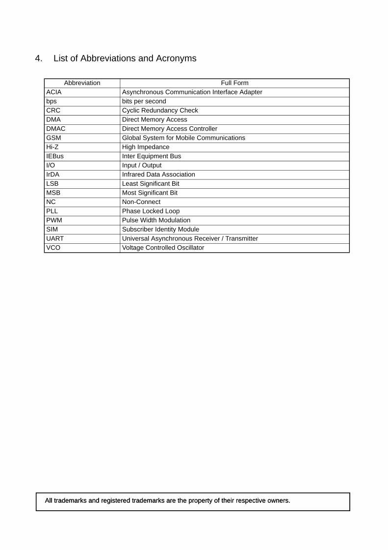
4. List of Abbreviations and Acronyms
Abbreviation Full FormACIA Asynchronous Communication Interface Adapterbps bits per secondCRC Cyclic Redundancy CheckDMA Direct Memory AccessDMAC Direct Memory Access ControllerGSM Global System for Mobile CommunicationsHi-Z High ImpedanceIEBus Inter Equipment BusI/O Input / OutputIrDA Infrared Data AssociationLSB Least Significant BitMSB Most Significant BitNC Non-ConnectPLL Phase Locked LoopPWM Pulse Width ModulationSIM Subscriber Identity ModuleUART Universal Asynchronous Receiver / TransmitterVCO Voltage Controlled Oscillator
All trademarks and registered trademarks are the property of their respective owners.All trademarks and registered trademarks are the property of their respective owners.

A - 1
Table of Contents
SFR Page Reference ........................................................................................................................... B - 1
1. Overview ......................................................................................................................................... 11.1 Applications ............................................................................................................................................... 11.2 Performance Overview .............................................................................................................................. 21.3 Block Diagram .......................................................................................................................................... 41.4 Product Information .................................................................................................................................. 51.5 Pin Assignments ........................................................................................................................................ 71.6 Pin Functions ............................................................................................................................................. 8
2. Central Processing Unit (CPU) ..................................................................................................... 102.1 Data Registers (R0, R1, R2 and R3) ....................................................................................................... 112.2 Address Registers (A0 and A1) ............................................................................................................... 112.3 Frame Base Register (FB) ....................................................................................................................... 112.4 Interrupt Table Register (INTB) .............................................................................................................. 112.5 Program Counter (PC) ............................................................................................................................. 112.6 User Stack Pointer (USP) and Interrupt Stack Pointer (ISP) .................................................................. 112.7 Static Base Register (SB) ........................................................................................................................ 112.8 Flag Register (FLG) ................................................................................................................................ 11
2.8.1 Carry Flag (C) ..................................................................................................................................... 112.8.2 Debug Flag (D) ................................................................................................................................... 112.8.3 Zero Flag (Z) ....................................................................................................................................... 112.8.4 Sign Flag (S) ....................................................................................................................................... 112.8.5 Register Bank Select Flag (B) ............................................................................................................ 112.8.6 Overflow Flag (O) .............................................................................................................................. 112.8.7 Interrupt Enable Flag (I) ..................................................................................................................... 122.8.8 Stack Pointer Select Flag (U) .............................................................................................................. 122.8.9 Processor Interrupt Priority Level (IPL) ............................................................................................. 122.8.10 Reserved Bit ........................................................................................................................................ 12
3. Memory ......................................................................................................................................... 133.1 R8C/22 Group ......................................................................................................................................... 133.2 R8C/23 Group ......................................................................................................................................... 14
4. Special Function Registers (SFRs) ............................................................................................... 15
5. Resets ........................................................................................................................................... 285.1 Hardware Reset ....................................................................................................................................... 31
5.1.1 When Power Supply is Stable ............................................................................................................. 315.1.2 Power On ............................................................................................................................................ 31
5.2 Power-On Reset Function ....................................................................................................................... 335.3 Voltage Monitor 1 Reset ......................................................................................................................... 345.4 Voltage Monitor 2 Reset ......................................................................................................................... 345.5 Watchdog Timer Reset ............................................................................................................................ 345.6 Software Reset ......................................................................................................................................... 34
6. Voltage Detection Circuit .............................................................................................................. 356.1 VCC Input Voltage .................................................................................................................................. 41
6.1.1 Monitoring Vdet1 ............................................................................................................................... 41

A - 2
6.1.2 Monitoring Vdet2 ............................................................................................................................... 416.2 Voltage Monitor 1 Reset ......................................................................................................................... 426.3 Voltage Monitor 2 Interrupt and Voltage Monitor 2 Reset ..................................................................... 43
7. Programmable I/O Ports ............................................................................................................... 457.1 Functions of Programmable I/O Ports ..................................................................................................... 457.2 Effect on Peripheral Functions ................................................................................................................ 467.3 Pins Other than Programmable I/O Ports ................................................................................................ 467.4 Port Settings ............................................................................................................................................ 577.5 Unassigned Pin Handling ........................................................................................................................ 68
8. Processor Mode ............................................................................................................................ 698.1 Processor Modes ...................................................................................................................................... 69
9. Bus ................................................................................................................................................ 70
10. Clock Generation Circuit ............................................................................................................... 7110.1 XIN Clock ............................................................................................................................................... 7910.2 On-Chip Oscillator Clocks ...................................................................................................................... 80
10.2.1 Low-Speed On-Chip Oscillator Clock ................................................................................................ 8010.2.2 High-Speed On-Chip Oscillator Clock ............................................................................................... 80
10.3 CPU Clock and Peripheral Function Clock ............................................................................................. 8110.3.1 System Clock ...................................................................................................................................... 8110.3.2 CPU Clock .......................................................................................................................................... 8110.3.3 Peripheral Function Clock (f1, f2, f4, f8, f32, and fCAN0) ............................................................... 8110.3.4 fOCO ................................................................................................................................................... 8110.3.5 fOCO40M ........................................................................................................................................... 8110.3.6 fOCO-F ............................................................................................................................................... 8110.3.7 fOCO-S ............................................................................................................................................... 8110.3.8 fOCO128 ............................................................................................................................................. 82
10.4 Power Control .......................................................................................................................................... 8310.4.1 Standard Operating Mode ................................................................................................................... 8310.4.2 Wait Mode .......................................................................................................................................... 8410.4.3 Stop Mode ........................................................................................................................................... 88
10.5 Oscillation Stop Detection Function ....................................................................................................... 9110.5.1 How to Use Oscillation Stop Detection Function ............................................................................... 91
10.6 Notes on Clock Generation Circuit ......................................................................................................... 9410.6.1 Stop Mode ........................................................................................................................................... 9410.6.2 Wait Mode .......................................................................................................................................... 9410.6.3 Oscillation Stop Detection Function ................................................................................................... 9410.6.4 Oscillation Circuit Constants .............................................................................................................. 94
11. Protection ...................................................................................................................................... 95
12. Interrupts ....................................................................................................................................... 9612.1 Interrupt Overview .................................................................................................................................. 96
12.1.1 Types of Interrupts .............................................................................................................................. 9612.1.2 Software Interrupts ............................................................................................................................. 9712.1.3 Special Interrupts ................................................................................................................................ 98

A - 3
12.1.4 Peripheral Function Interrupt .............................................................................................................. 9812.1.5 Interrupts and Interrupt Vector ........................................................................................................... 9912.1.6 Interrupt Control ............................................................................................................................... 101
12.2 INT Interrupt ......................................................................................................................................... 11012.2.1 INTi Interrupt (i = 0 to 3) .................................................................................................................. 11012.2.2 INTi Input Filter (i = 0 to 3) .............................................................................................................. 112
12.3 Key Input Interrupt ................................................................................................................................ 11312.4 CAN0 Wake-Up Interrupt ..................................................................................................................... 11512.5 Address Match Interrupt ........................................................................................................................ 11612.6 Timer RD Interrupt, Clock Synchronous Serial I/O with Chip Select Interrupts and I2C bus Interface
Interrupts (Interrupts with Multiple Interrupt Request Sources) ........................................................... 11812.7 Notes on Interrupts ................................................................................................................................ 120
12.7.1 Reading Address 00000h .................................................................................................................. 12012.7.2 SP Setting .......................................................................................................................................... 12012.7.3 External Interrupt and Key Input Interrupt ....................................................................................... 12012.7.4 Changing Interrupt Sources .............................................................................................................. 12112.7.5 Changing Interrupt Control Register Contents ................................................................................. 122
13. Watchdog Timer .......................................................................................................................... 12313.1 Count Source Protection Mode Disabled .............................................................................................. 12613.2 Count Source Protection Mode Enabled ............................................................................................... 127
14. Timers ......................................................................................................................................... 12814.1 Timer RA ............................................................................................................................................... 130
14.1.1 Timer Mode ...................................................................................................................................... 13414.1.2 Pulse Output Mode ........................................................................................................................... 13614.1.3 Event Counter Mode ......................................................................................................................... 13814.1.4 Pulse Width Measurement Mode ...................................................................................................... 14014.1.5 Pulse Period Measurement Mode ..................................................................................................... 14314.1.6 Notes on Timer RA ........................................................................................................................... 146
14.2 Timer RB ............................................................................................................................................... 14714.2.1 Timer Mode ...................................................................................................................................... 15114.2.2 Programmable Waveform Generation Mode .................................................................................... 15414.2.3 Programmable One-shot Generation Mode ...................................................................................... 15714.2.4 Programmable Wait One-shot Generation Mode ............................................................................. 16114.2.5 Notes on Timer RB ........................................................................................................................... 165
14.3 Timer RD ............................................................................................................................................... 16914.3.1 Count Source ..................................................................................................................................... 17414.3.2 Buffer Operation ............................................................................................................................... 17514.3.3 Synchronous Operation ..................................................................................................................... 17714.3.4 Pulse Output Forced Cutoff .............................................................................................................. 17814.3.5 Input Capture Function ..................................................................................................................... 18014.3.6 Output Compare Function ................................................................................................................ 19414.3.7 PWM Mode ....................................................................................................................................... 21014.3.8 Reset Synchronous PWM Mode ....................................................................................................... 22314.3.9 Complementary PWM Mode ............................................................................................................ 23314.3.10 PWM3 Mode ..................................................................................................................................... 24714.3.11 Timer RD Interrupt ........................................................................................................................... 25914.3.12 Notes on Timer RD ........................................................................................................................... 261

A - 4
14.4 Timer RE ............................................................................................................................................... 26714.4.1 Output Compare Mode ..................................................................................................................... 26814.4.2 Notes on Timer RE ........................................................................................................................... 274
15. Serial Interface ............................................................................................................................ 27515.1 Clock Synchronous Serial I/O Mode ..................................................................................................... 281
15.1.1 Polarity Select Function .................................................................................................................... 28415.1.2 LSB First/MSB First Select Function ............................................................................................... 28415.1.3 Continuous Receive Mode ................................................................................................................ 285
15.2 Clock Asynchronous Serial I/O (UART) Mode .................................................................................... 28615.2.1 Bit Rate ............................................................................................................................................. 290
15.3 Notes on Serial Interface ....................................................................................................................... 291
16. Clock Synchronous Serial Interface ............................................................................................ 29216.1 Mode Selection ...................................................................................................................................... 29216.2 Clock Synchronous Serial I/O with Chip Select (SSU) ........................................................................ 293
16.2.1 Transfer Clock .................................................................................................................................. 30216.2.2 SS Shift Register (SSTRSR) ............................................................................................................. 30416.2.3 Interrupt Requests ............................................................................................................................. 30516.2.4 Communication Modes and Pin Functions ....................................................................................... 30616.2.5 Clock Synchronous Communication Mode ...................................................................................... 30716.2.6 Operation in 4-Wire Bus Communication Mode .............................................................................. 31416.2.7 SCS Pin Control and Arbitration ...................................................................................................... 32016.2.8 Notes on Clock Synchronous Serial I/O with Chip Select ............................................................... 321
16.3 I2C Bus Interface ................................................................................................................................... 32216.3.1 Transfer Clock .................................................................................................................................. 33216.3.2 Interrupt Requests ............................................................................................................................. 33316.3.3 I2C Bus Interface Mode .................................................................................................................... 33416.3.4 Clock Synchronous Serial Mode ...................................................................................................... 34516.3.5 Noise Canceller ................................................................................................................................. 34816.3.6 Bit Synchronization Circuit .............................................................................................................. 34916.3.7 Examples of Register Setting ............................................................................................................ 35016.3.8 Notes on I2C Bus Interface ............................................................................................................... 354
17. Hardware LIN .............................................................................................................................. 35517.1 Features ................................................................................................................................................. 35517.2 Input/Output Pins .................................................................................................................................. 35617.3 Register Configuration .......................................................................................................................... 35717.4 Functional Description .......................................................................................................................... 359
17.4.1 Master Mode ..................................................................................................................................... 35917.4.2 Slave Mode ....................................................................................................................................... 36217.4.3 Bus Collision Detection Function ..................................................................................................... 36617.4.4 Hardware LIN End Processing ......................................................................................................... 367
17.5 Interrupt Requests .................................................................................................................................. 36817.6 Notes on Hardware LIN ........................................................................................................................ 369
18. CAN Module ............................................................................................................................... 37018.1 CAN Module-Related Registers ............................................................................................................ 37118.2 CAN0 Message Box .............................................................................................................................. 372

A - 5
18.3 Acceptance Mask Registers ................................................................................................................... 37418.4 CAN SFR Registers ............................................................................................................................... 375
18.4.1 C0MCTLi Register (i = 0 to 15) ....................................................................................................... 37518.4.2 C0CTLR Register ............................................................................................................................. 37618.4.3 C0STR Register ................................................................................................................................ 37718.4.4 C0SSTR Register .............................................................................................................................. 37818.4.5 C0ICR Register ................................................................................................................................. 37918.4.6 C0IDR Register ................................................................................................................................. 37918.4.7 C0CONR Register ............................................................................................................................ 38018.4.8 C0RECR Register ............................................................................................................................. 38118.4.9 C0TECR Register ............................................................................................................................. 38118.4.10 C0AFS Register ................................................................................................................................ 382
18.5 Operational Modes ................................................................................................................................ 38318.5.1 CAN Reset/Initialization Mode ........................................................................................................ 38318.5.2 CAN Operation Mode ....................................................................................................................... 38418.5.3 CAN Sleep Mode .............................................................................................................................. 38418.5.4 CAN Interface Sleep Mode ............................................................................................................... 38418.5.5 Bus-Off State .................................................................................................................................... 385
18.6 Configuration of the CAN Module System Clock ................................................................................ 38618.6.1 Bit Timing Configuration ................................................................................................................. 38618.6.2 Baud Rate .......................................................................................................................................... 387
18.7 Acceptance Filtering Function and Masking Function ......................................................................... 38818.8 Acceptance Filter Support Unit (ASU) ................................................................................................. 38918.9 Basic CAN Mode .................................................................................................................................. 39018.10 Return from Bus off Function ............................................................................................................... 39018.11 Listen-Only Mode ................................................................................................................................. 39018.12 Reception and Transmission ................................................................................................................. 391
18.12.1 Reception .......................................................................................................................................... 39218.12.2 Transmission ..................................................................................................................................... 393
18.13 CAN Interrupts ...................................................................................................................................... 39418.14 Notes on CAN Module .......................................................................................................................... 395
18.14.1 Reading C0STR Register .................................................................................................................. 39518.14.2 Performing CAN Configuration ....................................................................................................... 39718.14.3 Suggestions to Reduce Power Consumption .................................................................................... 398
19. A/D Converter ............................................................................................................................. 39919.1 One-Shot Mode ..................................................................................................................................... 40319.2 Repeat Mode .......................................................................................................................................... 40619.3 Sample and Hold ................................................................................................................................... 40919.4 A/D Conversion Cycles ......................................................................................................................... 41019.5 Internal Equivalent Circuit of Analog Input .......................................................................................... 41119.6 Output Impedance of Sensor Under A/D Conversion ........................................................................... 41219.7 Notes on A/D Converter ........................................................................................................................ 413
20. Flash Memory ............................................................................................................................. 41420.1 Overview ............................................................................................................................................... 41420.2 Memory Map ......................................................................................................................................... 41620.3 Functions to Prevent Rewriting of Flash Memory ................................................................................ 419
20.3.1 ID Code Check Function .................................................................................................................. 419

A - 6
20.3.2 ROM Code Protect Function ............................................................................................................ 42020.4 CPU Rewrite Mode ............................................................................................................................... 421
20.4.1 EW0 Mode ........................................................................................................................................ 42220.4.2 EW1 Mode ........................................................................................................................................ 42220.4.3 Software Commands ......................................................................................................................... 43120.4.4 Status Registers ................................................................................................................................. 43620.4.5 Full Status Check .............................................................................................................................. 437
20.5 Standard Serial I/O Mode ...................................................................................................................... 43920.5.1 ID Code Check Function .................................................................................................................. 439
20.6 Parallel I/O Mode .................................................................................................................................. 44320.6.1 ROM Code Protect Function ............................................................................................................ 443
20.7 Notes on Flash Memory ........................................................................................................................ 44420.7.1 CPU Rewrite Mode ........................................................................................................................... 444
21. Electrical Characteristics ............................................................................................................ 447
22. Usage Notes ............................................................................................................................... 46722.1 Notes on Clock Generation Circuit ....................................................................................................... 467
22.1.1 Stop Mode ......................................................................................................................................... 46722.1.2 Wait Mode ........................................................................................................................................ 46722.1.3 Oscillation Stop Detection Function ................................................................................................. 46722.1.4 Oscillation Circuit Constants ............................................................................................................ 467
22.2 Notes on Interrupts ................................................................................................................................ 46822.2.1 Reading Address 00000h .................................................................................................................. 46822.2.2 SP Setting .......................................................................................................................................... 46822.2.3 External Interrupt and Key Input Interrupt ....................................................................................... 46822.2.4 Changing Interrupt Sources .............................................................................................................. 46922.2.5 Changing Interrupt Control Register Contents ................................................................................. 470
22.3 Notes on Timers .................................................................................................................................... 47122.3.1 Notes on Timer RA ........................................................................................................................... 47122.3.2 Notes on Timer RB ........................................................................................................................... 47222.3.3 Notes on Timer RD ........................................................................................................................... 47622.3.4 Notes on Timer RE ........................................................................................................................... 482
22.4 Notes on Serial Interface ....................................................................................................................... 48322.5 Clock Synchronous Serial Interface ...................................................................................................... 484
22.5.1 Notes on Clock Synchronous Serial I/O with Chip Select ............................................................... 48422.5.2 Notes on I2C Bus Interface ............................................................................................................... 484
22.6 Notes on Hardware LIN ........................................................................................................................ 48522.7 Notes on CAN Module .......................................................................................................................... 486
22.7.1 Reading C0STR Register .................................................................................................................. 48622.7.2 Performing CAN Configuration ....................................................................................................... 48822.7.3 Suggestions to Reduce Power Consumption .................................................................................... 489
22.8 Notes on A/D Converter ....................................................................................................................... 49022.9 Notes on Flash Memory ........................................................................................................................ 491
22.9.1 CPU Rewrite Mode ........................................................................................................................... 49122.10 Notes on Noise ..................................................................................................................................... 494
22.10.1 Inserting a Bypass Capacitor between VCC and VSS Pins as a Countermeasure against Noise and Latch-up ............................................................................................................................................ 494
22.10.2 Countermeasures against Noise Error of Port Control Registers ..................................................... 494

A - 7
23. Notes on On-Chip Debugger ...................................................................................................... 495
24. Notes on Emulator Debugger ..................................................................................................... 496
Appendix 1. Package Dimensions ........................................................................................................ 497
Appendix 2. Connection Examples between Serial Writer and On-Chip Debugging Emulator ............ 498
Appendix 3. Example of Oscillation Evaluation Circuit ......................................................................... 499
Index ..................................................................................................................................................... 500

B - 1
SFR Page Reference
NOTE:1. Blank columns are all reserved space. No access is allowed.
Address Register Symbol Page0000h
0001h0002h
0003h
0004h Processor Mode Register 0 PM0 690005h Processor Mode Register 1 PM1 690006h System Clock Control Register 0 CM0 730007h System Clock Control Register 1 CM1 740008h
0009h
000Ah Protect Register PRCR 95000Bh
000Ch Oscillation Stop Detection Register OCD 75000Dh Watchdog Timer Reset Register WDTR 125000Eh Watchdog Timer Start Register WDTS 125000Fh Watchdog Timer Control Register WDC 1240010h Address Match Interrupt Register 0 RMAD0 1170011h
0012h
0013h Address Match Interrupt Enable Register AIER 1170014h Address Match Interrupt Register 1 RMAD1 1170015h
0016h0017h
0018h
0019h
001Ah001Bh
001Ch Count Source Protect Mode Register CSPR 125001Dh001Eh
001Fh
0020h0021h
0022h
0023h High-Speed On-Chip Oscillator Control Register 0 FRA0 760024h High-Speed On-Chip Oscillator Control Register 1 FRA1 760025h High-Speed On-Chip Oscillator Control Register 2 FRA2 770026h0027h
0028h
0029h002Ah
002Bh
002Ch002Dh
002Eh
002Fh0030h
0031h Voltage Detection Register 1 VCA1 380032h Voltage Detection Register 2 VCA2 38, 770033h
0034h
0035h0036h Voltage Monitor 1 Circuit Control Register VW1C 390037h Voltage Monitor 2 Circuit Control Register VW2C 400038h0039h
003Ah
003Bh003Ch
003Dh
003Eh003Fh
Address Register Symbol Page0040h
0041h0042h
0043h CAN0 Wake Up Interrupt Control Register C01WKIC 1010044h CAN0 Successful Reception Interrupt Control
RegisterC0RECIC 101
0045h CAN0 Successful Transmission Interrupt Control Register
C0TRMIC 101
0046h CAN0 State/Error Interrupt Control Register C01ERRIC 1010047h
0048h Timer RD0 Interrupt Control Register TRD0IC 1020049h Timer RD1 Interrupt Control Register TRD1IC 102004Ah Timer RE Interrupt Control Register TREIC 101004Bh
004Ch004Dh Key Input Interrupt Control Register KUPIC 101004Eh A/D Conversion Interrupt Control Register ADIC 101004Fh SSU Interrupt Control Register/IIC Bus
Interrupt Control RegisterSSUIC/IICIC 102
0050h0051h UART0 Transmit Interrupt Control Register S0TIC 1010052h UART0 Receive Interrupt Control Register S0RIC 1010053h UART1 Transmit Interrupt Control Register S1TIC 1010054h UART1 Receive Interrupt Control Register S1RIC 1010055h INT2 Interrupt Control Register INT2IC 1030056h Timer RA Interrupt Control Register TRAIC 1010057h
0058h Timer RB Interrupt Control Register TRBIC 1010059h INT1 Interrupt Control Register INT1IC 103005Ah INT3 Interrupt Control Register INT3IC 103005Bh
005Ch
005Dh INT0 Interrupt Control Register INT0IC 103005Eh
005Fh
0060h0061h
0062h
0063h0064h
0065h
0066h0067h
0068h
0069h006Ah
006Bh
006Ch006Dh
006Eh
006Fh0070h
0071h
0072h0073h
0074h
0075h0076h
0077h
0078h0079h
007Ah
007Bh007Ch
007Dh
007Eh007Fh

B - 2
NOTE:1. Blank columns are all reserved space. No access is allowed.
Address Register Symbol Page0080h
0081h
0082h0083h
0084h
0085h0086h
0087h
0088h0089h
008Ah
008Bh
008Ch008Dh
008Eh
008Fh0090h
0091h
0092h0093h
0094h
0095h0096h
0097h
0098h0099h
009Ah
009Bh009Ch
009Dh
009Eh009Fh
00A0h UART0 Transmit/Receive Mode Register U0MR 27800A1h UART0 Bit Rate Register U0BRG 27700A2h UART0 Transmit Buffer Register U0TB 27700A3h
00A4h UART0 Transmit/Receive Control Register 0 U0C0 27900A5h UART0 Transmit/Receive Control Register 1 U0C1 27900A6h UART0 Receive Buffer Register U0RB 27700A7h00A8h UART1 Transmit/Receive Mode Register U1MR 27800A9h UART1 Bit Rate Register U1BRG 27700AAh UART1 Transmit Buffer Register U1TB 27700ABh
00ACh UART1 Transmit/Receive Control Register 0 U1C0 27900ADh UART1 Transmit/Receive Control Register 1 U1C1 27900AEh UART1 Receive Buffer Register U1RB 27700AFh
00B0h00B1h
00B2h
00B3h00B4h
00B5h
00B6h00B7h
00B8h SS Control Register H/IIC Bus Control Register 1 SSCRH/ICCR1 295, 32500B9h SS Control Register L/IIC Bus Control Register 2 SSCRL/ICCR2 296, 32600BAh SS Mode Register/IIC Bus Mode Register 1 SSMR/ICMR 297, 32700BBh SS Enable Register/IIC Bus Interrupt Enable
RegisterSSER/ICIER 298, 328
00BCh SS Status Register/IIC Bus Status Register SSSR/ICSR 299, 32900BDh SS Mode Register 2/Slave Address Register SSMR2/SAR 300, 33000BEh SS Transmit Data Register/IIC Bus Transmit
Data RegisterSSTDR/ICDRT 301, 330
00BFh SS Receive Data Register/IIC Bus Receive Data Register
SSRDR/ICDRR
301, 331
Address Register Symbol Page00C0h A/D Register AD 40200C1h
00C2h00C3h
00C4h
00C5h00C6h
00C7h
00C8h00C9h
00CAh
00CBh
00CCh00CDh
00CEh
00CFh00D0h
00D1h
00D2h00D3h
00D4h A/D Control Register 2 ADCON2 40200D5h00D6h A/D Control Register 0 ADCON0 401, 404, 40700D7h A/D Control Register 1 ADCON1 402, 405, 40800D8h00D9h
00DAh
00DBh00DCh
00DDh
00DEh00DFh
00E0h Port P0 Register P0 5500E1h Port P1 Register P1 5500E2h Port P0 Direction Register PD0 5500E3h Port P1 Direction Register PD1 5500E4h Port P2 Register P2 5500E5h Port P3 Register P3 5500E6h Port P2 Direction Register PD2 5500E7h Port P3 Direction Register PD3 5500E8h Port P4 Register P4 5500E9h
00EAh Port P4 Direction Register PD4 5500EBh
00ECh Port P6 Register P6 5500EDh00EEh Port P6 Direction Register PD6 5500EFh
00F0h00F1h
00F2h
00F3h00F4h
00F5h UART1 Function Select Register U1SR 28000F6h00F7h
00F8h Port Mode Register PMR 56, 280, 301, 331
00F9h External Input Enable Register INTEN 11000FAh INT Input Filter Select Register INTF 11100FBh Key Input Enable Register KIEN 11400FCh Pull-Up Control Register 0 PUR0 5600FDh Pull-Up Control Register 1 PUR1 5600FEh
00FFh
B - 3
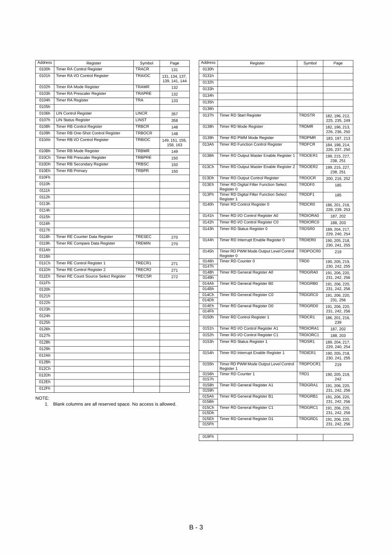
NOTE:1. Blank columns are all reserved space. No access is allowed.
Address Register Symbol Page0100h Timer RA Control Register TRACR 1310101h Timer RA I/O Control Register TRAIOC 131, 134, 137,
139, 141, 1440102h Timer RA Mode Register TRAMR 1320103h Timer RA Prescaler Register TRAPRE 1320104h Timer RA Register TRA 1330105h
0106h LIN Control Register LINCR 3570107h LIN Status Register LINST 3580108h Timer RB Control Register TRBCR 1480109h Timer RB One-Shot Control Register TRBOCR 148010Ah Timer RB I/O Control Register TRBIOC 149, 151, 155,
158, 163010Bh Timer RB Mode Register TRBMR 149010Ch Timer RB Prescaler Register TRBPRE 150010Dh Timer RB Secondary Register TRBSC 150010Eh Timer RB Primary TRBPR 150010Fh
0110h0111h
0112h
0113h0114h
0115h
0116h0117h
0118h Timer RE Counter Data Register TRESEC 2700119h Timer RE Compare Data Register TREMIN 270011Ah
011Bh
011Ch Timer RE Control Register 1 TRECR1 271011Dh Timer RE Control Register 2 TRECR2 271011Eh Timer RE Count Source Select Register TRECSR 272011Fh0120h
0121h
0122h0123h
0124h
0125h0126h
0127h
0128h0129h
012Ah
012Bh012Ch
012Dh
012Eh012Fh
Address Register Symbol Page0130h
0131h
0132h0133h
0134h
0135h0136h
0137h Timer RD Start Register TRDSTR 182, 196, 212, 225, 235, 249
0138h Timer RD Mode Register TRDMR 182, 196, 213, 226, 236, 250
0139h Timer RD PWM Mode Register TRDPMR 183, 197, 213013Ah Timer RD Function Control Register TRDFCR 184, 198, 214,
226, 237, 250013Bh Timer RD Output Master Enable Register 1 TRDOER1 199, 215, 227,
238, 251013Ch Timer RD Output Master Enable Register 2 TRDOER2 199, 215, 227,
238, 251013Dh Timer RD Output Control Register TRDOCR 200, 216, 252013Eh Timer RD Digital Filter Function Select
Register 0TRDDF0 185
013Fh Timer RD Digital Filter Function Select Register 1
TRDDF1 185
0140h Timer RD Control Register 0 TRDCR0 186, 201, 216, 228, 239, 253
0141h Timer RD I/O Control Register A0 TRDIORA0 187, 2020142h Timer RD I/O Control Register C0 TRDIORC0 188, 2030143h Timer RD Status Register 0 TRDSR0 189, 204, 217,
229, 240, 2540144h Timer RD Interrupt Enable Register 0 TRDIER0 190, 205, 218,
230, 241, 2550145h Timer RD PWM Mode Output Level Control
Register 0TRDPOCR0 219
0146h Timer RD Counter 0 TRD0 190, 205, 219, 230, 242, 2550147h
0148h Timer RD General Register A0 TRDGRA0 191, 206, 220, 231, 242, 2560149h
014Ah Timer RD General Register B0 TRDGRB0 191, 206, 220, 231, 242, 256014Bh
014Ch Timer RD General Register C0 TRDGRC0 191, 206, 220, 231, 256014Dh
014Eh Timer RD General Register D0 TRDGRD0 191, 206, 220, 231, 242, 256014Fh
0150h Timer RD Control Register 1 TRDCR1 186, 201, 216, 239
0151h Timer RD I/O Control Register A1 TRDIORA1 187, 2020152h Timer RD I/O Control Register C1 TRDIORC1 188, 2030153h Timer RD Status Register 1 TRDSR1 189, 204, 217,
229, 240, 2540154h Timer RD Interrupt Enable Register 1 TRDIER1 190, 205, 218,
230, 241, 2550155h Timer RD PWM Mode Output Level Control
Register 1TRDPOCR1 219
0156h Timer RD Counter 1 TRD1 190, 205, 219, 2420157h
0158h Timer RD General Register A1 TRDGRA1 191, 206, 220, 231, 242, 2560159h
015Ah Timer RD General Register B1 TRDGRB1 191, 206, 220, 231, 242, 256015Bh
015Ch Timer RD General Register C1 TRDGRC1 191, 206, 220, 231, 242, 256015Dh
015Eh Timer RD General Register D1 TRDGRD1 191, 206, 220, 231, 242, 256015Fh
019Fh

B - 4
NOTE:1. Blank columns are all reserved space. No access is allowed.
Address Register Symbol Page01A0h
01A1h
01A2h01A3h
01A4h
01A5h01A6h
01A7h
01A8h01A9h
01AAh
01ABh
01ACh01ADh
01AEh
01AFh01B0h
01B1h
01B2h01B3h Flash Memory Control Register 4 FMR4 42701B4h
01B5h Flash Memory Control Register 1 FMR1 42601B6h
01B7h Flash Memory Control Register 0 FMR0 42501B8h01B9h
01BAh
01BBh
01FFh
1300h CAN0 Message Control Register 0 C0MCTL0 3751301h CAN0 Message Control Register 1 C0MCTL1 3751302h CAN0 Message Control Register 2 C0MCTL2 3751303h CAN0 Message Control Register 3 C0MCTL3 3751304h CAN0 Message Control Register 4 C0MCTL4 3751305h CAN0 Message Control Register 5 C0MCTL5 3751306h CAN0 Message Control Register 6 C0MCTL6 3751307h CAN0 Message Control Register 7 C0MCTL7 3751308h CAN0 Message Control Register 8 C0MCTL8 3751309h CAN0 Message Control Register 9 C0MCTL9 375130Ah CAN0 Message Control Register 10 C0MCTL10 375130Bh CAN0 Message Control Register 11 C0MCTL11 375130Ch CAN0 Message Control Register 12 C0MCTL12 375130Dh CAN0 Message Control Register 13 C0MCTL13 375130Eh CAN0 Message Control Register 14 C0MCTL14 375130Fh CAN0 Message Control Register 15 C0MCTL15 3751310h CAN0 Control Register C0CTLR 3761311h1312h CAN0 Status Register C0STR 3771313h
1314h CAN0 Slot Status Register C0SSTR 3781315h
1316h CAN0 Interrupt Control Register C0ICR 3791317h1318h CAN0 Extended ID Register C0IDR 3791319h
131Ah CAN0 Configuration Register C0CONR 380131Bh
131Ch CAN0 Receive Error Count Register C0RECR 381131Dh CAN0 Transmit Error Count Register C0TECR 381131Eh131Fh
133Fh
Address Register Symbol Page1340h
1341h
1342h CAN0 Acceptance Filter Support Register C0AFS 3821343h
1344h
1345h1346h
1347h
1348h1349h
134Ah
134Bh
134Ch134Dh
134Eh
134Fh1350h
1351h
1352h1353h
1354h
1355h1356h
1357h
1358h1359h
135Ah
135Bh135Ch
135Dh
135Eh135Fh CAN0 Clock Select Register CCLKR 78
1360h CAN0 Slot 0: Identifier/DLC
372, 373
1361h
1362h
1363h1364h
1365h
1366h CAN0 Slot 0: Data Field1367h
1368h
1369h136Ah
136Bh
136Ch136Dh
136Eh CAN0 Slot 0: Time Stamp
136Fh1370h CAN0 Slot 1: Identifier/DLC
1371h
1372h1373h
1374h
1375h1376h CAN0 Slot 1: Data Field
1377h
1378h1379h
137Ah
137Bh
137Ch137Dh
137Eh CAN0 Slot 1: Time Stamp
137Fh

B - 5
NOTE:1. Blank columns are all reserved space. No access is allowed.
Address Register Symbol Page
1380h CAN0 Slot 2: Identifier/DLC
372, 373
1381h1382h
1383h
1384h1385h
1386h CAN0 Slot 2: Data Field
1387h1388h
1389h
138Ah
138Bh138Ch
138Dh
138Eh CAN0 Slot 2: Time Stamp138Fh
1390h CAN0 Slot 3: Identifier/DLC
1391h1392h
1393h
1394h1395h
1396h CAN0 Slot 3: Data Field
1397h1398h
1399h
139Ah139Bh
139Ch
139Dh139Eh CAN0 Slot 3: Time Stamp
139Fh
13A0h CAN0 Slot 4: Identifier/DLC13A1h
13A2h
13A3h13A4h
13A5h
13A6h CAN0 Slot 4: Data Field13A7h
13A8h
13A9h13AAh
13ABh
13ACh13ADh
13AEh CAN0 Slot 4: Time Stamp
13AFh13B0h CAN0 Slot 5: Identifier/DLC
13B1h
13B2h13B3h
13B4h
13B5h13B6h CAN0 Slot 5: Data Field
13B7h
13B8h13B9h
13BAh
13BBh
13BCh13BDh
13BEh CAN0 Slot 5: Time Stamp
13BFh
Address Register Symbol Page
13C0h CAN0 Slot 6: Identifier/DLC
372, 373
13C1h13C2h
13C3h
13C4h13C5h
13C6h CAN0 Slot 6: Data Field
13C7h13C8h
13C9h
13CAh
13CBh13CCh
13CDh
13CEh CAN0 Slot 6: Time Stamp13CFh
13D0h CAN0 Slot 7: Identifier/DLC
13D1h13D2h
13D3h
13D4h13D5h
13D6h CAN0 Slot 7: Data Field
13D7h13D8h
13D9h
13DAh13DBh
13DCh
13DDh13DEh CAN0 Slot 7: Time Stamp
13DFh
13E0h CAN0 Slot 8: Identifier/DLC13E1h
13E2h
13E3h13E4h
13E5h
13E6h CAN0 Slot 8: Data Field13E7h
13E8h
13E9h13EAh
13EBh
13ECh13EDh
13EEh CAN0 Slot 8: Time Stamp
13EFh13F0h CAN0 Slot 9: Identifier/DLC
13F1h
13F2h13F3h
13F4h
13F5h13F6h CAN0 Slot 9: Data Field
13F7h
13F8h13F9h
13FAh
13FBh
13FCh13FDh
13FEh CAN0 Slot 9: Time Stamp
13FFh

B - 6
NOTE:1. Blank columns are all reserved space. No access is allowed.
Address Register Symbol Page
1400h CAN0 Slot 10: Identifier/DLC
372, 373
1401h1402h
1403h
1404h1405h
1406h CAN0 Slot 10: Data Field
1407h1408h
1409h
140Ah
140Bh140Ch
140Dh
140Eh CAN0 Slot 10: Time Stamp140Fh
1410h CAN0 Slot 11: Identifier/DLC
1411h1412h
1413h
1414h1415h
1416h CAN0 Slot 11: Data Field
1417h1418h
1419h
141Ah141Bh
141Ch
141Dh141Eh CAN0 Slot 11: Time Stamp
141Fh
1420h CAN0 Slot 12: Identifier/DLC1421h
1422h
1423h1424h
1425h
1426h CAN0 Slot 12: Data Field1427h
1428h
1429h142Ah
142Bh
142Ch142Dh
142Eh CAN0 Slot 12: Time Stamp
142Fh1430h CAN0 Slot 13: Identifier/DLC
1431h
1432h1433h
1434h
1435h1436h CAN0 Slot 13: Data Field
1437h
1438h1439h
143Ah
143Bh
143Ch143Dh
143Eh CAN0 Slot 13: Time Stamp
143Fh
Address Register Symbol Page
1440h CAN0 Slot 14: Identifier/DLC
372, 373
1441h1442h
1443h
1444h1445h
1446h CAN0 Slot 14: Data Field
1447h1448h
1449h
144Ah
144Bh144Ch
144Dh
144Eh CAN0 Slot 14: Time Stamp144Fh
1450h CAN0 Slot 15: Identifier/DLC
1451h1452h
1453h
1454h1455h
1456h CAN0 Slot 15: Data Field
1457h1458h
1459h
145Ah145Bh
145Ch
145Dh145Eh CAN0 Slot 15: Time Stamp
145Fh
1460h CAN0 Global Mask Register C0GMR
374
1461h
1462h
1463h1464h
1465h
1466h CAN0 Local Mask A Register C0LMAR1467h
1468h
1469h146Ah
146Bh
146Ch CAN0 Local Mask B Register C0LMBR146Dh
146Eh
146Fh1470h
1471h1472h
1473h1474h
1475h
FFFFh Option Function Select Register OFS 30, 124, 420

Rev.2.00 Aug 20, 2008 Page 1 of 501REJ09B0251-0200
R8C/22 Group, R8C/23 GroupRENESAS MCU
1. OverviewThis MCU is built using the high-performance silicon gate CMOS process using the R8C CPU core and is packagedin a 48-pin plastic molded LQFP. This MCU operates using sophisticated instructions featuring a high level ofinstruction efficiency. With 1 Mbyte of address space, it is capable of executing instructions at high speed. This MCUis equipped with one CAN module and suited to in-vehicle or FA networking.Furthermore, the data flash (1 KB x 2 blocks) is embedded in the R8C/23 Group.The difference between R8C/22 and R8C/23 Groups is only the existence of the data flash. Their peripheral functionsare the same.
1.1 ApplicationsAutomotive, etc.
REJ09B0251-0200Rev.2.00
Aug 20, 2008

R8C/22 Group, R8C/23 Group 1. Overview
Rev.2.00 Aug 20, 2008 Page 2 of 501REJ09B0251-0200
1.2 Performance OverviewTable 1.1 outlines the Functions and Specifications for R8C/22 Group and Table 1.2 outlines the Functions andSpecifications for R8C/23 Group.
NOTES:1. When using options, be sure to inquire about the specification.2. I2C bus is a registered trademark of Koninklijke Philips Electronics N.V.
Table 1.1 Functions and Specifications for R8C/22 GroupItem Specification
CPU Number of fundamental instructions 89 instructionsMinimum instruction execution time 50 ns (f(XIN) = 20 MHz, VCC = 3.0 to 5.5 V)
100 ns (f(XIN) = 10 MHz, VCC = 2.7 to 5.5 V)Operating mode Single-chipAddress space 1 MbyteMemory capacity Refer to Table 1.3 Product Information for R8C/22 Group
Peripheral Function
Ports I/O ports: 41 pins, Input port: 3 pinsTimers Timer RA: 8 bits x 1 channel,
Timer RB: 8 bits x 1 channel(Each timer equipped with 8-bit prescaler)
Timer RD: 16 bits x 2 channel(Circuits of input capture and output compare)
Timer RE: With compare match functionSerial interface 1 channel (UART0)
Clock synchronous I/O, UART1 channel (UART1)
UARTClock synchronous serial interface 1 channel
I2C bus interface(2), Clock synchronous serial I/O with chip select
LIN module Hardware LIN: 1 channel(timer RA, UART0)
CAN module 1 channel with 2.0B specification: 16 slotsA/D converter 10-bit A/D converter: 1 circuit, 12 channelsWatchdog timer 15 bits x 1 channel (with prescaler)
Reset start selectableInterrupt Internal: 14 sources, External: 6 sources, Software: 4 sources,
Priority level: 7 levelsClock generation circuits 2 circuits
XIN clock generation circuit (with on-chip feedback resistor)On-chip oscillator (high speed, low speed)High-speed on-chip oscillator has frequency adjustmentfunction.
Oscillation stop detection function
Stop detection of XIN clock oscillation
Voltage detection circuit On-chipPower-on reset circuit include On-chip
Electric Characteristics
Supply voltage VCC = 3.0 to 5.5 V (f(XIN) = 20 MHz)(D, J version)VCC = 3.0 to 5.5 V (f(XIN) = 16 MHz)(K version)VCC = 2.7 to 5.5 V (f(XIN) = 10 MHz)
Current consumption Typ. 12.5 mA (VCC = 5 V, f(XIN) = 20 MHz, High-speed on-chip oscillator stopping)Typ. 6.0 mA (VCC = 5 V, f(XIN) = 10 MHz, High-speed on-chip oscillator stopping)
Flash Memory Programming and erasure voltage VCC = 2.7 to 5.5 VProgramming and erasure endurance
100 times
Operating Ambient Temperature -40 to 85°C-40 to 125°C (option(1))
Package 48-pin mold-plastic LQFP

R8C/22 Group, R8C/23 Group 1. Overview
Rev.2.00 Aug 20, 2008 Page 3 of 501REJ09B0251-0200
NOTES:1. When using options, be sure to inquire about the specification.2. I2C bus is a registered trademark of Koninklijke Philips Electronics N.V.
Table 1.2 Functions and Specifications for R8C/23 GroupItem Specification
CPU Number of fundamental instructions 89 instructionsMinimum instruction execution time 50 ns (f(XIN) = 20 MHz, VCC = 3.0 to 5.5 V)
100 ns (f(XIN) = 10 MHz, VCC = 2.7 to 5.5 V)Operating mode Single-chipAddress space 1 MbyteMemory capacity Refer to Table 1.4 Product Information for R8C/23 Group
Peripheral Function
Ports I/O ports: 41 pins, Input port: 3 pinsTimers Timer RA: 8 bits x 1 channel,
Timer RB: 8 bits x 1 channel (Each timer equipped with 8-bit prescaler)
Timer RD: 16 bits x 2 channel(Circuits of input capture and output compare)
Timer RE: With compare match functionSerial interface 1 channel (UART0)
Clock synchronous I/O, UART1 channel (UART1)
UARTClock synchronous serial interface 1 channel
I2C bus interface(2), Clock synchronous serial I/O with chip select
LIN module Hardware LIN: 1 channel(Timer RA, UART0)
CAN module 1 channel with 2.0B specification: 16 slotsA/D converter 10-bit A/D converter: 1 circuit, 12 channelsWatchdog timer 15 bits x 1 channel (with prescaler)
Reset start selectableInterrupts Internal: 14 sources, External: 6 sources, Software: 4 sources,
Priority level: 7 levelsClock generation circuits 2 circuits
XIN clock generation circuit (with on-chip feedback resistor)On-chip oscillator (high speed, low speed)High-speed on-chip oscillator has frequency adjustmentfunction.
Oscillation stop detection function
Stop detection of XIN clock oscillation
Voltage detection circuit On-chipPower-on reset circuit include On-chip
Electric Characteristics
Supply voltage VCC = 3.0 to 5.5 V (f(XIN) = 20 MHz)(D, J version)VCC = 3.0 to 5.5 V (f(XIN) = 16 MHz)(K version)VCC = 2.7 to 5.5 V (f(XIN) = 10 MHz)
Current consumption Typ. 12.5 mA (VCC = 5 V, f(XIN) = 20 MHz, High-speed on-chip oscillator stopping)Typ. 6.0 mA (VCC = 5 V, f(XIN) = 10 MHz, High-speed on-chip oscillator stopping)
Flash Memory Programming and erasure voltage VCC = 2.7 to 5.5 VProgramming and erasure endurance
10,000 times (data flash)1,000 times (program ROM)
Operating Ambient Temperature -40 to 85°C-40 to 125°C (option(1))
Package 48-pin mold-plastic LQFP

R8C/22 Group, R8C/23 Group 1. Overview
Rev.2.00 Aug 20, 2008 Page 4 of 501REJ09B0251-0200
1.3 Block DiagramFigure 1.1 shows a Block Diagram.
Figure 1.1 Block Diagram
R8C CPU core
Timer
Timer RA (8 bits)Timer RB (8 bits)
Timer RD (16 bits × 2 channels)Timer RE (8 bits)
A/D converter(10 bits × 12 channels)
System clockgeneration circuit
XIN-XOUTHigh-speed on-chip oscillatorLow-speed on-chip oscillator
UART orclock synchronous serial I/O
(8 bits × 1 channel)
MemoryWatchdog timer(15 bits)
ROM(1)
RAM(2)
Multiplier
R0H R0LR1H
R2R3
R1L
A0A1FB
SBUSPISP
INTBPC
FLG
I/O port
NOTES:1. ROM size depends on MCU type.2. RAM size depends on MCU type.
I2C bus interface orclock synchronous serial I/O
with chip select(8 bits × 1 channel)
8
Port P1
6
Port P3
3 3
Port P4
8
Port P0
8
Port P2
8
Port P6
CAN module(1 channel)
UART(8 bits × 1 channel)
LIN module(1 channel)

R8C/22 Group, R8C/23 Group 1. Overview
Rev.2.00 Aug 20, 2008 Page 5 of 501REJ09B0251-0200
1.4 Product InformationTable 1.3 lists Product Information for R8C/22 Group and Table 1.4 lists Product Information for R8C/23 Group.
NOTE:1. Do not use addresses 20000h to 23FFFh because these areas are used for the emulator debugger.
Refer to 24. Notes on Emulator Debugger.
Figure 1.2 Type Number, Memory Size, and Package of R8C/22 Group
Table 1.3 Product Information for R8C/22 Group Current of Aug. 2008 Type No. ROM Capacity RAM Capacity Package Type Remarks
R5F21226DFP 32 Kbytes 2 Kbytes PLQP0048KB-A D version Flash memory versionR5F21227DFP 48 Kbytes 2.5 Kbytes PLQP0048KB-A
R5F21228DFP 64 Kbytes 3 Kbytes PLQP0048KB-AR5F21226JFP 32 Kbytes 2 Kbytes PLQP0048KB-A J versionR5F21227JFP 48 Kbytes 2.5 Kbytes PLQP0048KB-AR5F21228JFP 64 Kbytes 3 Kbytes PLQP0048KB-AR5F2122AJFP 96 Kbytes 5 Kbytes PLQP0048KB-AR5F2122CJFP 128 Kbytes(1) 6 Kbytes PLQP0048KB-AR5F21226KFP 32 Kbytes 2 Kbytes PLQP0048KB-A K versionR5F21227KFP 48 Kbytes 2.5 Kbytes PLQP0048KB-AR5F21228KFP 64 Kbytes 3 Kbytes PLQP0048KB-AR5F2122AKFP 96 Kbytes 5 Kbytes PLQP0048KB-AR5F2122CKFP 128 Kbytes(1) 6 Kbytes PLQP0048KB-A
Part number R 5 F 21 22 6 J XXX FPPackage type:
FP: PLQP0048KB-A(0.5 mm pin-pitch, 7 mm square body)
ROM number
ClassificationD: Operating ambient temperature -40°C to 85°C (D version)J: Operating ambient temperature -40°C to 85°C (J version)K: Operating ambient temperature -40°C to 125°C (K version)
ROM capacity6: 32 KB7: 48 KB8: 64 KBA: 96 KBC: 128 KB
R8C/22 Group
R8C/2x Series
Memory typeF: Flash memory version
Renesas MCU
Renesas semiconductors

R8C/22 Group, R8C/23 Group 1. Overview
Rev.2.00 Aug 20, 2008 Page 6 of 501REJ09B0251-0200
NOTE:1. Do not use addresses 20000h to 23FFFh because these areas are used for the emulator debugger.
Refer to 24. Notes on Emulator Debugger.
Figure 1.3 Type Number, Memory Size, and Package of R8C/23 Group
Table 1.4 Product Information for R8C/23 Group Current of Aug. 2008
Type No.ROM Capacity
RAM Capacity Package Type RemarksProgram ROM Data Flash
R5F21236DFP 32 Kbytes 1 Kbyte X 2 2 Kbytes PLQP0048KB-A D version Flash memory version
R5F21237DFP 48 Kbytes 1 Kbyte X 2 2.5 Kbytes PLQP0048KB-AR5F21238DFP 64 Kbytes 1 Kbyte X 2 3 Kbytes PLQP0048KB-AR5F21236JFP 32 Kbytes 1 Kbyte X 2 2 Kbytes PLQP0048KB-A J versionR5F21237JFP 48 Kbytes 1 Kbyte X 2 2.5 Kbytes PLQP0048KB-AR5F21238JFP 64 Kbytes 1 Kbyte X 2 3 Kbytes PLQP0048KB-AR5F2123AJFP 96 Kbytes 1 Kbyte X 2 5 Kbytes PLQP0048KB-AR5F2123CJFP 128 Kbytes(1) 1 Kbyte X 2 6 Kbytes PLQP0048KB-AR5F21236KFP 32 Kbytes 1 Kbyte X 2 2 Kbytes PLQP0048KB-A K versionR5F21237KFP 48 Kbytes 1 Kbyte X 2 2.5 Kbytes PLQP0048KB-AR5F21238KFP 64 Kbytes 1 Kbyte X 2 3 Kbytes PLQP0048KB-AR5F2123AKFP 96 Kbytes 1 Kbyte X 2 5 Kbytes PLQP0048KB-AR5F2123CKFP 128 Kbytes(1) 1 Kbyte X 2 6 Kbytes PLQP0048KB-A
Part number R 5 F 21 23 6 J XXX FPPackage type:
FP: PLQP0048KB-A(0.5 mm pin-pitch, 7 mm square body)
ROM number
ClassificationD: Operating ambient temperature -40°C to 85°C (D version)J: Operating ambient temperature -40°C to 85°C (J version)K: Operating ambient temperature -40°C to 125°C (K version)
ROM capacity6: 32 KB7: 48 KB8: 64 KBA: 96 KBC: 128 KB
R8C/23 Group
R8C/2x Series
Memory typeF: Flash memory version
Renesas MCU
Renesas semiconductors

R8C/22 Group, R8C/23 Group 1. Overview
Rev.2.00 Aug 20, 2008 Page 7 of 501REJ09B0251-0200
1.5 Pin AssignmentsFigure 1.4 shows Pin Assignments (Top View).
Figure 1.4 Pin Assignments (Top View)
48P3_7/SSO
47P0_0/AN7
46P0_1/AN6
45P0_2/AN5
44P0_3/AN4
43P6_1/CTX0
42P6_2/CRX0
41P6_0/TREO
40P4_2/VREF
39P0_4/AN3
38P0_5/AN2
37P0_6/AN1
13
14
15
16
17
18
19
20
21
22
23
24
P2_6/TRDIOC1
P2_5/TRDIOB1
P2_4/TRDIOA1
P2_3/TRDIOD0
P2_2/TRDIOC0
P2_1/TRDIOB0
P2_0/TRDIOA0/TRDCLK
P1_7/TRAIO/INT1
P1_6/CLK0
P1_5/RXD0/(TRAIO)/(INT1)(2)
P1_4/TXD0
P1_3/KI3/AN11
12P
2_7/
TRD
IOD
1
11V
CC
/AV
CC
10P
4_6/
XIN
9V
SS
/AV
SS
8(1
) P4_
7/X
OU
T
7R
ES
ET
6P
4_4
5P
4_3
4M
OD
E
3P
3_4/
SD
A/S
CS
2P
3_3/
SS
I
1P
3_5/
SC
L/S
SC
K
252627282930313233343536
P4_
5/IN
T0
P6_
6/IN
T2/T
XD
1
P6_
7/IN
T3/R
XD
1
P1_
2/K
I2/A
N10
P1_
1/K
I1/A
N9
P1_
0/K
I0/A
N8
P3_
1/TR
BO
P3_
0/TR
AO
P6_
5
P6_
4
P6_
3
P0_
7/A
N0
Pin assignments (top view)
Package: PLQP0048KB-A0.5 mm pin pitch, 7 mm square body
R8C/22 Group,R8C/23 Group
NOTES:1. P4_7 is an input-only port.2. Can be assigned to the pin in parentheses by a program.3. Confirm the pin 1 position on the package by referring to the package dimensions.

R8C/22 Group, R8C/23 Group 1. Overview
Rev.2.00 Aug 20, 2008 Page 8 of 501REJ09B0251-0200
1.6 Pin FunctionsTable 1.5 lists the Pin Functions and Table 1.6 lists the Pin Name Information by Pin Number.
I: Input O: Output I/O: Input and output
Table 1.5 Pin Functions
Type Symbol I/O Type DescriptionPower Supply Input VCC
VSSI Apply 2.7 V to 5.5 V to the VCC pin. Apply 0 V to the
VSS pin.Analog Power Supply Input
AVCC, AVSS I Applies the power supply for the A/D converter. Connect a capacitor between AVCC and AVSS.
Reset Input RESET I Input “L” on this pin resets the MCU.MODE MODE I Connect this pin to VCC via a resistor.XIN Clock Input XIN I These pins are provided for the XIN clock generation
circuit I/O. Connect a ceramic resonator or a crystaloscillator between the XIN and XOUT pins. To use anexternally derived clock, input it to the XIN pin and leavethe XOUT pin open.
XIN Clock Output XOUT O
INT Interrupt Input INT0 to INT3 I INT interrupt input pins.INT0 Timer RD input pins. INT1 Timer RA input pins.
Key Input Interrupt KI0 to KI3 I Key input interrupt input pins.Timer RA TRAIO I/O Timer RA I/O pin.
TRAO O Timer RA output pin.Timer RB TRBO O Timer RB output pin.Timer RD TRDIOA0, TRDIOA1,
TRDIOB0, TRDIOB1, TRDIOC0, TRDIOC1, TRDIOD0, TRDIOD1
I/O Timer RD I/O ports.
TRDCLK I External clock input pin.Timer RE TREO O Divided clock output pin.Serial Interface CLK0 I/O Transfer clock I/O pin.
RXD0, RXD1 I Serial data input pins.TXD0, TXD1 O Serial data output pins.
I2C Bus Interface SCL I/O Clock I/O pin.SDA I/O Data I/O pin.
Clock Synchronous Serial I/O with Chip Select
SSI I/O Data I/O pin.SCS I/O Chip-select signal I/O pin.SSCK I/O Clock I/O pin.SSO I/O Data I/O pin.
CAN Module CRX0 I CAN data input pin.CTX0 O CAN data output pin.
Reference Voltage Input VREF I Reference voltage input pin to A/D converter.A/D Converter AN0 to AN11 I Analog input pins to A/D converter.I/O Port P0_0 to P0_7,
P1_0 to P1_7, P2_0 to P2_7, P3_0, P3_1, P3_3 to P3_5, P3_7, P4_3 to P4_5, P6_0 to P6_7
I/O CMOS I/O ports. Each port contains an input/outputselect direction register, allowing each pin in that port tobe directed for input or output individually.Any port set to input can select whether to use a pull-upresistor or not by a program.
Input Port P4_2, P4_6, P4_7 I Input only ports.

R8C/22 Group, R8C/23 Group 1. Overview
Rev.2.00 Aug 20, 2008 Page 9 of 501REJ09B0251-0200
NOTE:1. Can be assigned to the pin in parentheses by a program.
Table 1.6 Pin Name Information by Pin Number
Pin Number Control Pin Port
I/O Pin Functions for of Peripheral Modules
Interrupt Timer Serial Interface
Clock Synchronous Serial I/O with
Chip Select
I2C Bus Interface
CAN Module
A/D Converter
1 P3_5 SSCK SCL2 P3_3 SSI3 P3_4 SCS SDA4 MODE5 P4_36 P4_47 RESET8 XOUT P4_79 VSS/AVSS
10 XIN P4_611 VCC/AVCC12 P2_7 TRDIOD113 P2_6 TRDIOC114 P2_5 TRDIOB115 P2_4 TRDIOA116 P2_3 TRDIOD017 P2_2 TRDIOC018 P2_1 TRDIOB019 P2_0 TRDIOA0/TRDCLK20 P1_7 INT1 TRAIO21 P1_6 CLK022 P1_5 (INT1)(1) (TRAIO)(1) RXD023 P1_4 TXD024 P1_3 KI3 AN1125 P4_5 INT0 INT026 P6_6 INT2 TXD127 P6_7 INT3 RXD128 P1_2 KI2 AN1029 P1_1 KI1 AN930 P1_0 KI0 AN831 P3_1 TRBO32 P3_0 TRAO33 P6_534 P6_435 P6_336 P0_7 AN037 P0_6 AN138 P0_5 AN239 P0_4 AN340 VREF P4_241 P6_0 TREO42 P6_2 CRX043 P6_1 CTX044 P0_3 AN445 P0_2 AN546 P0_1 AN647 P0_0 AN748 P3_7 SSO

R8C/22 Group, R8C/23 Group 2. Central Processing Unit (CPU)
Rev.2.00 Aug 20, 2008 Page 10 of 501REJ09B0251-0200
2. Central Processing Unit (CPU)Figure 2.1 shows the CPU Registers. The CPU contains 13 registers. Of these, R0, R1, R2, R3, A0, A1, and FBcomprise a register bank. Two sets of register banks are provided.
Figure 2.1 CPU Registers
R2b31 b15 b8b7 b0
Data registers(1)
Address registers(1)
R3R0H (high-order of R0)
R2R3A0A1
INTBHb15b19 b0
INTBL
FB Frame base registers(1)
The 4-high order bits of INTB are INTBH andthe 16-low order bits of INTB are INTBL.
Interrupt table register
b19 b0
USP
Program counter
ISPSB
User stack pointer
Interrupt stack pointer
Static base register
PC
FLG Flag register
Carry flagDebug flagZero flagSign flagRegister bank select flagOverflow flagInterrupt enable flagStack pointer select flagReserved areaProcessor interrupt priority levelReserved area
CIPL DZSBOIU
b15 b0
b15 b0
b15 b0b8 b7
NOTE:1. A register bank comprises these registers. Two sets of register banks are provided.
R0L (low-order of R0)
R1H (high-order of R1) R1L (low-order of R1)

R8C/22 Group, R8C/23 Group 2. Central Processing Unit (CPU)
Rev.2.00 Aug 20, 2008 Page 11 of 501REJ09B0251-0200
2.1 Data Registers (R0, R1, R2 and R3)R0 is a 16-bit register for transfer, arithmetic, and logic operations. The same applies to R1 to R3.R0 can be split into high-order bit (R0H) and low-order bit (R0L) to be used separately as 8-bit data registers. Thesame applies to R1H and R1L as R0H and R0L. R2 can be combined with R0 to be used as a 32-bit data register(R2R0). The same applies R3R1 as R2R0.
2.2 Address Registers (A0 and A1)A0 is a 16-bit register for address register indirect addressing and address register relative addressing. They alsoare used for transfer, arithmetic and logic operations. The same applies to A1 as A0. A1 can be combined with A0 to be used a 32-bit address register (A1A0).
2.3 Frame Base Register (FB)FB is a 16-bit register for FB relative addressing.
2.4 Interrupt Table Register (INTB)INTB, a 20-bit register, indicates the start address of an interrupt vector table.
2.5 Program Counter (PC)PC, 20 bits wide, indicates the address of an instruction to be executed.
2.6 User Stack Pointer (USP) and Interrupt Stack Pointer (ISP)The stack pointer (SP), USP and ISP, are 16 bits wide each.The U flag of FLG is used to switch between USP and ISP.
2.7 Static Base Register (SB)SB is a 16-bit register for SB relative addressing.
2.8 Flag Register (FLG)FLG is a 11-bit register indicating the CPU status.
2.8.1 Carry Flag (C)The C flag retains a carry, borrow, or shift-out bit that has occurred in the arithmetic and logic unit.
2.8.2 Debug Flag (D)The D flag is for debug only. Set to 0.
2.8.3 Zero Flag (Z)The Z flag is set to 1 when an arithmetic operation resulted in 0; otherwise, 0.
2.8.4 Sign Flag (S)The S flag is set to 1 when an arithmetic operation resulted in a negative value; otherwise, 0.
2.8.5 Register Bank Select Flag (B)The register bank 0 is selected when the B flag is 0. The register bank 1 is selected when this flag is set to 1.
2.8.6 Overflow Flag (O)The O flag is set to 1 when the operation resulted in an overflow; otherwise, 0.

R8C/22 Group, R8C/23 Group 2. Central Processing Unit (CPU)
Rev.2.00 Aug 20, 2008 Page 12 of 501REJ09B0251-0200
2.8.7 Interrupt Enable Flag (I)The I flag enables a maskable interrupt.An interrupt is disabled when the I flag is set to 0, and are enabled when the I flag is set to 1. The I flag is set to0 when an interrupt request is acknowledged.
2.8.8 Stack Pointer Select Flag (U)ISP is selected when the U flag is set to 0; USP is selected when the U flag is set to 1.The U flag is set to 0 when a hardware interrupt request is acknowledged or the INT instruction of softwareinterrupt numbers. 0 to 31 is executed.
2.8.9 Processor Interrupt Priority Level (IPL)IPL, 3 bits wide, assigns processor interrupt priority levels from level 0 to level 7.If a requested interrupt has greater priority than IPL, the interrupt is enabled.
2.8.10 Reserved BitIf necessary, set to 0. When read, the content is undefined.

R8C/22 Group, R8C/23 Group 3. Memory
Rev.2.00 Aug 20, 2008 Page 13 of 501REJ09B0251-0200
3. Memory
3.1 R8C/22 GroupFigure 3.1 shows a Memory Map of R8C/22 Group. The R8C/22 Group has 1 Mbyte of address space fromaddress 00000h to FFFFFh.The internal ROM is allocated lower addresses, beginning with address 0FFFFh. For example, a 48-Kbyte internalROM is allocated addresses 04000h to 0FFFFh.The fixed interrupt vector table is allocated addresses 0FFDCh to 0FFFFh. They store the starting address of eachinterrupt routine. The internal RAM is allocated higher addresses, beginning with address 00400h. For example, a 2.5-Kbyteinternal RAM is allocated addresses 00400h to 00DFFh. The internal RAM is used not only for storing data butalso for calling subroutines and as stacks when interrupt requests are acknowledged.Special function registers (SFR) are allocated addresses 00000h to 002FFh and 01300h to 0147Fh (SFR area forCAN). The peripheral function control registers are allocated here. All addresses within the SFR, which havenothing allocated are reserved for future user and cannot be accessed by users.
Figure 3.1 Memory Map of R8C/22 Group
Undefined instructionOverflow
BRK instructionAddress match
Single stepWatchdog timer•oscillation stop detection•voltage detection
Address break(Reserved)
Reset
FFFFFh
0FFFFh
0YYYYh
0XXXXh
00400h
002FFh
00000h
Internal ROM(program ROM)
Internal RAM
SFR(Refer to 4. SpecialFunction Registers
(SFRs))
0FFFFh
0FFDCh
NOTES:1. SFR area for CAN is allocated addresses 01300h to 0147Fh.2. The blank regions are reserved. Do not access locations in these regions.3. Do not use addresses 20000h to 23FFFh because these areas are used for the emulator debugger. Refer to 24. Notes on
Emulator Debugger.
Reserved area(1)01300h02000h
Internal ROM(3)
(program ROM)
Part NumberInternal ROM
Size Address 0YYYYh Address ZZZZZhR5F21226DFP, R5F21226JFP, R5F21226KFPR5F21227DFP, R5F21227JFP, R5F21227KFPR5F21228DFP, R5F21228JFP, R5F21228KFPR5F2122AJFP, R5F2122AKFPR5F2122CJFP, R5F2122CKFP
32 Kbytes48 Kbytes64 Kbytes96 Kbytes128 Kbytes
08000h04000h04000h04000h04000h
--
13FFFh1BFFFh23FFFh
Internal RAM
Address 0XXXXh00BFFh00DFFh00FFFh00FFFh00FFFh
2 Kbytes2.5 Kbytes3 Kbytes5 Kbytes6 Kbytes
Size
ZZZZZh
Internal RAM03000h
0SSSSh
Address 0SSSSh---
037FFh03BFFh

R8C/22 Group, R8C/23 Group 3. Memory
Rev.2.00 Aug 20, 2008 Page 14 of 501REJ09B0251-0200
3.2 R8C/23 GroupFigure 3.2 shows a Memory Map of R8C/23 Group. The R8C/23 Group has 1 Mbyte of address space fromaddress 00000h to FFFFFh.The internal ROM (program ROM) is allocated lower addresses, beginning with address 0FFFFh. For example, a48-Kbyte internal ROM is allocated addresses 04000h to 0FFFFh.The fixed interrupt vector table is allocated addresses 0FFDCh to 0FFFFh. They store the starting address of eachinterrupt routine.The internal ROM (data flash) is allocated addresses 02400h to 02BFFh.The internal RAM is allocated higher addresses, beginning with address 00400h. For example, a 2.5-Kbyteinternal RAM is allocated addresses 00400h to 00DFFh. The internal RAM is used not only for storing data butalso for calling subroutines and as stacks when interrupt requests are acknowledged.Special function registers (SFR) are allocated addresses 00000h to 002FFh and 01300h to 0147Fh (SFR area forCAN). The peripheral function control registers are allocated them. All addresses within the SFR, which havenothing allocated are reserved for future use and cannot be accessed by users.
Figure 3.2 Memory Map of R8C/23 Group
Undefined instructionOverflow
BRK instructionAddress match
Single stepWatchdog timer•oscillation stop detection•voltage detection
Address break(Reserved)
Reset
FFFFFh
0FFFFh
0YYYYh
0XXXXh
00400h
002FFh
00000h
Internal ROM(program ROM)
Internal RAM
SFR(Refer to 4. SpecialFunction Registers
(SFRs))
0FFFFh
0FFDCh
02BFFh
02400hInternal ROM(data flash)(1)
Reserved area(2)01300h02000h
Internal ROM(4)
(program ROM)ZZZZZh
NOTES:1. Data flash block A (1 Kbyte) and B (1 Kbyte) are shown.2. SFR area for CAN is allocated addresses 01300h to 0147Fh.3. The blank regions are reserved. Do not access locations in these regions.4. Do not use addresses 20000h to 23FFFh because these areas are used for the emulator debugger. Refer to 24. Notes on
Emulator Debugger.
Part NumberInternal ROM
Size Address 0YYYYh Address ZZZZZhR5F21236DFP, R5F21236JFP, R5F21236KFPR5F21237DFP, R5F21237JFP, R5F21237KFPR5F21238DFP, R5F21238JFP, R5F21238KFPR5F2123AJFP, R5F2123AKFPR5F2123CJFP, R5F2123CKFP
32 Kbytes48 Kbytes64 Kbytes96 Kbytes
128 Kbytes
08000h04000h04000h04000h04000h
--
13FFFh1BFFFh23FFFh
Internal RAM
Address 0XXXXh00BFFh00DFFh00FFFh00FFFh00FFFh
2 Kbytes2.5 Kbytes3 Kbytes5 Kbytes6 Kbytes
Size Address 0SSSSh---
037FFh03BFFh
Internal RAM03000h0SSSSh

R8C/22 Group, R8C/23 Group 4. Special Function Registers (SFRs)
Rev.2.00 Aug 20, 2008 Page 15 of 501REJ09B0251-0200
4. Special Function Registers (SFRs)An SFR (special function register) is a control register for a peripheral function. Table 4.1 to Table 4.13 list the SFR Information.
Table 4.1 SFR Information (1)(1)
X: UndefinedNOTES:
1. The blank regions are reserved. Do not access locations in these regions.2. Software reset, watchdog timer reset, and voltage monitor 2 reset do not affect this register.3. The LVD0ON bit in the OFS register is set to 1.4. Power-on reset, voltage monitor 1 reset or the LVD0ON bit in the OFS register is set to 0.5. Software reset, watchdog timer reset, and voltage monitor 2 reset do not affect b2 and b3.6. Software reset, watchdog timer reset, and voltage monitor 2 reset do not affect b7.7. Software reset, the watchdog timer rest, and the voltage monitor 2 reset do not affect other than the b0 and b6.8. The CSPROINI bit in the OFS register is 0.
Address Register Symbol After reset0000h0001h0002h0003h0004h Processor Mode Register 0 PM0 00h0005h Processor Mode Register 1 PM1 00h0006h System Clock Control Register 0 CM0 01101000b0007h System Clock Control Register 1 CM1 00100000b0008h0009h000Ah Protect Register PRCR 00h000Bh000Ch Oscillation Stop Detection Register OCD 00000100b000Dh Watchdog Timer Reset Register WDTR XXh000Eh Watchdog Timer Start Register WDTS XXh000Fh Watchdog Timer Control Register WDC 00X11111b0010h Address Match Interrupt Register 0 RMAD0 00h0011h 00h0012h 00h0013h Address Match Interrupt Enable Register AIER 00h0014h Address Match Interrupt Register 1 RMAD1 00h0015h 00h0016h 00h0017h0018h0019h001Ah001Bh001Ch Count Source Protect Mode Register CSPR 00h
10000000b(8)
001Dh001Eh001Fh0020h0021h0022h0023h High-Speed On-Chip Oscillator Control Register 0 FRA0 00h0024h High-Speed On-Chip Oscillator Control Register 1 FRA1 When shipping0025h High-Speed On-Chip Oscillator Control Register 2 FRA2 00h0026h
0030h0031h Voltage Detection Register 1(2) VCA1 00001000b0032h Voltage Detection Register 2(6) VCA2 00h(3)
01000000b(4)
0033h0034h0035h0036h Voltage Monitor 1 Circuit Control Register(7) VW1C 0000X000b(3)
0100X001b(4)
0037h Voltage Monitor 2 Circuit Control Register(5) VW2C 00h0038h0039h
003Fh

R8C/22 Group, R8C/23 Group 4. Special Function Registers (SFRs)
Rev.2.00 Aug 20, 2008 Page 16 of 501REJ09B0251-0200
Table 4.2 SFR Information (2)(1)
X: UndefinedNOTES:
1. The blank regions are reserved. Do not access locations in these regions.2. Selected by the IICSEL bit in the PMR register.
Address Register Symbol After reset0040h0041h0042h0043h CAN0 Wake Up Interrupt Control Register C01WKIC XXXXX000b0044h CAN0 Successful Reception Interrupt Control Register C0RECIC XXXXX000b0045h CAN0 Successful Transmission Interrupt Control Register C0TRMIC XXXXX000b0046h CAN0 State/Error Interrupt Control Register C01ERRIC XXXXX000b0047h0048h Timer RD0 Interrupt Control Register TRD0IC XXXXX000b0049h Timer RD1 Interrupt Control Register TRD1IC XXXXX000b004Ah Timer RE Interrupt Control Register TREIC XXXXX000b004Bh004Ch004Dh Key Input Interrupt Control Register KUPIC XXXXX000b004Eh A/D Conversion Interrupt Control Register ADIC XXXXX000b004Fh SSU Interrupt Control Register/IIC Bus Interrupt Control Register(2) SSUIC/IICIC XXXXX000b0050h0051h UART0 Transmit Interrupt Control Register S0TIC XXXXX000b0052h UART0 Receive Interrupt Control Register S0RIC XXXXX000b0053h UART1 Transmit Interrupt Control Register S1TIC XXXXX000b0054h UART1 Receive Interrupt Control Register S1RIC XXXXX000b0055h INT2 Interrupt Control Register INT2IC XX00X000b0056h Timer RA Interrupt Control Register TRAIC XXXXX000b0057h0058h Timer RB Interrupt Control Register TRBIC XXXXX000b0059h INT1 Interrupt Control Register INT1IC XX00X000b005Ah INT3 Interrupt Control Register INT3IC XX00X000b005Bh005Ch005Dh INT0 Interrupt Control Register INT0IC XX00X000b005Eh005Fh0060h0061h0062h0063h0064h0065h0066h0067h0068h0069h006Ah006Bh006Ch006Dh006Eh006Fh0070h0071h0072h0073h0074h0075h0076h0077h0078h0079h007Ah007Bh007Ch007Dh007Eh007Fh

R8C/22 Group, R8C/23 Group 4. Special Function Registers (SFRs)
Rev.2.00 Aug 20, 2008 Page 17 of 501REJ09B0251-0200
Table 4.3 SFR Information (3)(1)
X: UndefinedNOTES:
1. The blank regions are reserved. Do not access locations in these regions.2. Selected by the IICSEL bit in the PMR register.
Address Register Symbol After reset0080h0081h0082h0083h0084h0085h0086h0087h0088h0089h008Ah008Bh008Ch008Dh008Eh008Fh0090h0091h0092h0093h0094h0095h0096h0097h0098h0099h009Ah009Bh009Ch009Dh009Eh009Fh00A0h UART0 Transmit/Receive Mode Register U0MR 00h00A1h UART0 Bit Rate Register U0BRG XXh00A2h UART0 Transmit Buffer Register U0TB XXh00A3h XXh00A4h UART0 Transmit/Receive Control Register 0 U0C0 00001000b00A5h UART0 Transmit/Receive Control Register 1 U0C1 00000010b00A6h UART0 Receive Buffer Register U0RB XXh00A7h XXh00A8h UART1 Transmit/Receive Mode Register U1MR 00h00A9h UART1 Bit Rate Register U1BRG XXh00AAh UART1 Transmit Buffer Register U1TB XXh00ABh XXh00ACh UART1 Transmit/Receive Control Register 0 U1C0 00001000b00ADh UART1 Transmit/Receive Control Register 1 U1C1 00000010b00AEh UART1 Receive Buffer Register U1RB XXh00AFh XXh00B0h00B1h00B2h00B3h00B4h00B5h00B6h00B7h00B8h SS Control Register H/IIC Bus Control Register 1(2) SSCRH/ICCR1 00h00B9h SS Control Register L/IIC Bus Control Register 2(2) SSCRL/ICCR2 01111101b00BAh SS Mode Register/IIC Bus Mode Register 1(2) SSMR/ICMR 00011000b00BBh SS Enable Register/IIC Bus Interrupt Enable Register(2) SSER/ICIER 00h00BCh SS Status Register/IIC Bus Status Register(2) SSSR/ICSR 00h/0000X000b00BDh SS Mode Register 2/Slave Address Register(2) SSMR2/SAR 00h00BEh SS Transmit Data Register/IIC Bus Transmit Data Register(2) SSTDR/ICDRT FFh00BFh SS Receive Data Register/IIC Bus Receive Data Register(2) SSRDR/ICDRR FFh

R8C/22 Group, R8C/23 Group 4. Special Function Registers (SFRs)
Rev.2.00 Aug 20, 2008 Page 18 of 501REJ09B0251-0200
Table 4.4 SFR Information (4)(1)
X: UndefinedNOTE:
1. The blank regions are reserved. Do not access locations in these regions.
Address Register Symbol After reset00C0h A/D Register AD XXh00C1h XXh00C2h00C3h00C4h00C5h00C6h00C7h00C8h00C9h00CAh00CBh00CCh00CDh00CEh00CFh00D0h00D1h00D2h00D3h00D4h A/D Control Register 2 ADCON2 00h00D5h00D6h A/D Control Register 0 ADCON0 00h00D7h A/D Control Register 1 ADCON1 00h00D8h00D9h00DAh00DBh00DCh00DDh00DEh00DFh00E0h Port P0 Register P0 XXh00E1h Port P1 Register P1 XXh00E2h Port P0 Direction Register PD0 00h00E3h Port P1 Direction Register PD1 00h00E4h Port P2 Register P2 XXh00E5h Port P3 Register P3 XXh00E6h Port P2 Direction Register PD2 00h00E7h Port P3 Direction Register PD3 00h00E8h Port P4 Register P4 XXh00E9h00EAh Port P4 Direction Register PD4 00h00EBh00ECh Port P6 Register P6 XXh00EDh00EEh Port P6 Direction Register PD6 00h00EFh00F0h00F1h00F2h00F3h00F4h00F5h UART1 Function Select Register U1SR XXh00F6h00F7h00F8h Port Mode Register PMR 00h00F9h External Input Enable Register INTEN 00h00FAh INT Input Filter Select Register INTF 00h00FBh Key Input Enable Register KIEN 00h00FCh Pull-Up Control Register 0 PUR0 00h00FDh Pull-Up Control Register 1 PUR1 XX00XX00b00FEh00FFh

R8C/22 Group, R8C/23 Group 4. Special Function Registers (SFRs)
Rev.2.00 Aug 20, 2008 Page 19 of 501REJ09B0251-0200
Table 4.5 SFR Information (5)(1)
X: UndefinedNOTE:
1. The blank regions are reserved. Do not access locations in these regions.
Address Register Symbol After reset0100h Timer RA Control Register TRACR 00h0101h Timer RA I/O Control Register TRAIOC 00h0102h Timer RA Mode Register TRAMR 00h0103h Timer RA Prescaler Register TRAPRE FFh0104h Timer RA Register TRA FFh0105h0106h LIN Control Register LINCR 00h0107h LIN Status Register LINST 00h0108h Timer RB Control Register TRBCR 00h0109h Timer RB One-Shot Control Register TRBOCR 00h010Ah Timer RB I/O Control Register TRBIOC 00h010Bh Timer RB Mode Register TRBMR 00h010Ch Timer RB Prescaler Register TRBPRE FFh010Dh Timer RB Secondary Register TRBSC FFh010Eh Timer RB Primary TRBPR FFh010Fh0110h0111h0112h0113h0114h0115h0116h0117h0118h Timer RE Counter Data Register TRESEC 00h0119h Timer RE Compare Data Register TREMIN 00h011Ah011Bh011Ch Timer RE Control Register 1 TRECR1 00h011Dh Timer RE Control Register 2 TRECR2 00h011Eh Timer RE Count Source Select Register TRECSR 00001000b011Fh0120h0121h0122h0123h0124h0125h0126h0127h0128h0129h012Ah012Bh012Ch012Dh012Eh012Fh0130h0131h0132h0133h0134h0135h0136h0137h Timer RD Start Register TRDSTR 11111100b0138h Timer RD Mode Register TRDMR 00001110b0139h Timer RD PWM Mode Register TRDPMR 10001000b013Ah Timer RD Function Control Register TRDFCR 10000000b013Bh Timer RD Output Master Enable Register 1 TRDOER1 FFh013Ch Timer RD Output Master Enable Register 2 TRDOER2 01111111b013Dh Timer RD Output Control Register TRDOCR 00h013Eh Timer RD Digital Filter Function Select Register 0 TRDDF0 00h013Fh Timer RD Digital Filter Function Select Register 1 TRDDF1 00h

R8C/22 Group, R8C/23 Group 4. Special Function Registers (SFRs)
Rev.2.00 Aug 20, 2008 Page 20 of 501REJ09B0251-0200
Table 4.6 SFR Information (6)(1)
X: UndefinedNOTE:
1. The blank regions are reserved. Do not access locations in these regions.
Address Register Symbol After reset0140h Timer RD Control Register 0 TRDCR0 00h0141h Timer RD I/O Control Register A0 TRDIORA0 10001000b0142h Timer RD I/O Control Register C0 TRDIORC0 10001000b0143h Timer RD Status Register 0 TRDSR0 11100000b0144h Timer RD Interrupt Enable Register 0 TRDIER0 11100000b0145h Timer RD PWM Mode Output Level Control Register 0 TRDPOCR0 11111000b0146h Timer RD Counter 0 TRD0 00h0147h 00h0148h Timer RD General Register A0 TRDGRA0 FFh0149h FFh014Ah Timer RD General Register B0 TRDGRB0 FFh014Bh FFh014Ch Timer RD General Register C0 TRDGRC0 FFh014Dh FFh014Eh Timer RD General Register D0 TRDGRD0 FFh014Fh FFh0150h Timer RD Control Register 1 TRDCR1 00h0151h Timer RD I/O Control Register A1 TRDIORA1 10001000b0152h Timer RD I/O Control Register C1 TRDIORC1 10001000b0153h Timer RD Status Register 1 TRDSR1 11000000b0154h Timer RD Interrupt Enable Register 1 TRDIER1 11100000b0155h Timer RD PWM Mode Output Level Control Register 1 TRDPOCR1 11111000b0156h Timer RD Counter 1 TRD1 00h0157h 00h0158h Timer RD General Register A1 TRDGRA1 FFh0159h FFh015Ah Timer RD General Register B1 TRDGRB1 FFh015Bh FFh015Ch Timer RD General Register C1 TRDGRC1 FFh015Dh FFh015Eh Timer RD General Register D1 TRDGRD1 FFh015Fh FFh0160h0161h0162h0163h0164h0165h0166h0167h0168h0169h016Ah016Bh016Ch016Dh016Eh016Fh0170h0171h0172h0173h0174h0175h0176h0177h0178h0179h017Ah017Bh017Ch017Dh017Eh017Fh

R8C/22 Group, R8C/23 Group 4. Special Function Registers (SFRs)
Rev.2.00 Aug 20, 2008 Page 21 of 501REJ09B0251-0200
Table 4.7 SFR Information (7)(1)
X: UndefinedNOTE:
1. The blank regions are reserved. Do not access locations in these regions.
Address Register Symbol After reset0180h0181h0182h0183h0184h0185h0186h0187h0188h0189h018Ah018Bh018Ch018Dh018Eh018Fh0190h0191h0192h0193h0194h0195h0196h0197h0198h0199h019Ah019Bh019Ch019Dh019Eh019Fh01A0h01A1h01A2h01A3h01A4h01A5h01A6h01A7h01A8h01A9h01AAh01ABh01ACh01ADh01AEh01AFh01B0h01B1h01B2h01B3h Flash Memory Control Register 4 FMR4 01000000b01B4h01B5h Flash Memory Control Register 1 FMR1 1000000Xb01B6h01B7h Flash Memory Control Register 0 FMR0 00000001b01B8h01B9h01BAh01BBh
01FDh01FEh01FFh

R8C/22 Group, R8C/23 Group 4. Special Function Registers (SFRs)
Rev.2.00 Aug 20, 2008 Page 22 of 501REJ09B0251-0200
Table 4.8 SFR Information (8)(1)
X: UndefinedNOTE:
1. The blank regions are reserved. Do not access locations in these regions.
Address Register Symbol After reset1300h CAN0 Message Control Register 0 C0MCTL0 00h1301h CAN0 Message Control Register 1 C0MCTL1 00h1302h CAN0 Message Control Register 2 C0MCTL2 00h1303h CAN0 Message Control Register 3 C0MCTL3 00h1304h CAN0 Message Control Register 4 C0MCTL4 00h1305h CAN0 Message Control Register 5 C0MCTL5 00h1306h CAN0 Message Control Register 6 C0MCTL6 00h1307h CAN0 Message Control Register 7 C0MCTL7 00h1308h CAN0 Message Control Register 8 C0MCTL8 00h1309h CAN0 Message Control Register 9 C0MCTL9 00h130Ah CAN0 Message Control Register 10 C0MCTL10 00h130Bh CAN0 Message Control Register 11 C0MCTL11 00h130Ch CAN0 Message Control Register 12 C0MCTL12 00h130Dh CAN0 Message Control Register 13 C0MCTL13 00h130Eh CAN0 Message Control Register 14 C0MCTL14 00h130Fh CAN0 Message Control Register 15 C0MCTL15 00h1310h CAN0 Control Register C0CTLR X0000001b1311h XX0X0000b1312h CAN0 Status Register C0STR 00h1313h X0000001b1314h CAN0 Slot Status Register C0SSTR 00h1315h 00h1316h CAN0 Interrupt Control Register C0ICR 00h1317h 00h1318h CAN0 Extended ID Register C0IDR 00h1319h 00h131Ah CAN0 Configuration Register C0CONR XXh131Bh XXh131Ch CAN0 Receive Error Count Register C0RECR 00h131Dh CAN0 Transmit Error Count Register C0TECR 00h131Eh131Fh1320h1321h1322h1323h1324h1325h1326h1327h1328h1329h132Ah132Bh132Ch132Dh132Eh132Fh1330h1331h1332h1333h1334h1335h1336h1337h1338h1339h133Ah133Bh133Ch133Dh133Eh133Fh

R8C/22 Group, R8C/23 Group 4. Special Function Registers (SFRs)
Rev.2.00 Aug 20, 2008 Page 23 of 501REJ09B0251-0200
Table 4.9 SFR Information (9)(1)
X: UndefinedNOTE:
1. The blank regions are reserved. Do not access locations in these regions.
Address Register Symbol After reset1340h1341h1342h CAN0 Acceptance Filter Support Register C0AFS XXh1343h XXh1344h1345h1346h1347h1348h1349h134Ah134Bh134Ch134Dh134Eh134Fh1350h1351h1352h1353h1354h1355h1356h1357h1358h1359h135Ah135Bh135Ch135Dh135Eh135Fh CAN0 Clock Select Register CCLKR 00h1360h CAN0 Slot 0: Identifier/DLC XXh1361h XXh1362h XXh1363h XXh1364h XXh1365h XXh1366h CAN0 Slot 0: Data Field XXh1367h XXh1368h XXh1369h XXh136Ah XXh136Bh XXh136Ch XXh136Dh XXh136Eh CAN0 Slot 0: Time Stamp XXh136Fh XXh1370h CAN0 Slot 1: Identifier/DLC XXh1371h XXh1372h XXh1373h XXh1374h XXh1375h XXh1376h CAN0 Slot 1: Data Field XXh1377h XXh1378h XXh1379h XXh137Ah XXh137Bh XXh137Ch XXh137Dh XXh137Eh CAN0 Slot 1: Time Stamp XXh137Fh XXh

R8C/22 Group, R8C/23 Group 4. Special Function Registers (SFRs)
Rev.2.00 Aug 20, 2008 Page 24 of 501REJ09B0251-0200
Table 4.10 SFR Information (10)(1)
X: UndefinedNOTE:
1. The blank regions are reserved. Do not access locations in these regions.
Address Register Symbol After reset1380h CAN0 Slot 2: Identifier/DLC XXh1381h XXh1382h XXh1383h XXh1384h XXh1385h XXh1386h CAN0 Slot 2: Data Field XXh1387h XXh1388h XXh1389h XXh138Ah XXh138Bh XXh138Ch XXh138Dh XXh138Eh CAN0 Slot 2: Time Stamp XXh138Fh XXh1390h CAN0 Slot 3: Identifier/DLC XXh1391h XXh1392h XXh1393h XXh1394h XXh1395h XXh1396h CAN0 Slot 3: Data Field XXh1397h XXh1398h XXh1399h XXh139Ah XXh139Bh XXh139Ch XXh139Dh XXh139Eh CAN0 Slot 3: Time Stamp XXh139Fh XXh13A0h CAN0 Slot 4: Identifier/DLC XXh13A1h XXh13A2h XXh13A3h XXh13A4h XXh13A5h XXh13A6h CAN0 Slot 4: Data Field XXh13A7h XXh13A8h XXh13A9h XXh13AAh XXh13ABh XXh13ACh XXh13ADh XXh13AEh CAN0 Slot 4: Time Stamp XXh13AFh XXh13B0h CAN0 Slot 5: Identifier/DLC XXh13B1h XXh13B2h XXh13B3h XXh13B4h XXh13B5h XXh13B6h CAN0 Slot 5: Data Field XXh13B7h XXh13B8h XXh13B9h XXh13BAh XXh13BBh XXh13BCh XXh13BDh XXh13BEh CAN0 Slot 5: Time Stamp XXh13BFh XXh

R8C/22 Group, R8C/23 Group 4. Special Function Registers (SFRs)
Rev.2.00 Aug 20, 2008 Page 25 of 501REJ09B0251-0200
Table 4.11 SFR Information (11)(1)
X: UndefinedNOTE:
1. The blank regions are reserved. Do not access locations in these regions.
Address Register Symbol After reset13C0h CAN0 Slot 6: Identifier/DLC XXh13C1h XXh13C2h XXh13C3h XXh13C4h XXh13C5h XXh13C6h CAN0 Slot 6: Data Field XXh13C7h XXh13C8h XXh13C9h XXh13CAh XXh13CBh XXh13CCh XXh13CDh XXh13CEh CAN0 Slot 6: Time Stamp XXh13CFh XXh13D0h CAN0 Slot 7: Identifier/DLC XXh13D1h XXh13D2h XXh13D3h XXh13D4h XXh13D5h XXh13D6h CAN0 Slot 7: Data Field XXh13D7h XXh13D8h XXh13D9h XXh13DAh XXh13DBh XXh13DCh XXh13DDh XXh13DEh CAN0 Slot 7: Time Stamp XXh13DFh XXh13E0h CAN0 Slot 8: Identifier/DLC XXh13E1h XXh13E2h XXh13E3h XXh13E4h XXh13E5h XXh13E6h CAN0 Slot 8: Data Field XXh13E7h XXh13E8h XXh13E9h XXh13EAh XXh13EBh XXh13ECh XXh13EDh XXh13EEh CAN0 Slot 8: Time Stamp XXh13EFh XXh13F0h CAN0 Slot 9: Identifier/DLC XXh13F1h XXh13F2h XXh13F3h XXh13F4h XXh13F5h XXh13F6h CAN0 Slot 9: Data Field XXh13F7h XXh13F8h XXh13F9h XXh13FAh XXh13FBh XXh13FCh XXh13FDh XXh13FEh CAN0 Slot 9: Time Stamp XXh13FFh XXh

R8C/22 Group, R8C/23 Group 4. Special Function Registers (SFRs)
Rev.2.00 Aug 20, 2008 Page 26 of 501REJ09B0251-0200
Table 4.12 SFR Information (12)(1)
X: UndefinedNOTE:
1. The blank regions are reserved. Do not access locations in these regions.
Address Register Symbol After reset1400h CAN0 Slot 10: Identifier/DLC XXh1401h XXh1402h XXh1403h XXh1404h XXh1405h XXh1406h CAN0 Slot 10: Data Field XXh1407h XXh1408h XXh1409h XXh140Ah XXh140Bh XXh140Ch XXh140Dh XXh140Eh CAN0 Slot 10: Time Stamp XXh140Fh XXh1410h CAN0 Slot 11: Identifier/DLC XXh1411h XXh1412h XXh1413h XXh1414h XXh1415h XXh1416h CAN0 Slot 11: Data Field XXh1417h XXh1418h XXh1419h XXh141Ah XXh141Bh XXh141Ch XXh141Dh XXh141Eh CAN0 Slot 11: Time Stamp XXh141Fh XXh1420h CAN0 Slot 12: Identifier/DLC XXh1421h XXh1422h XXh1423h XXh1424h XXh1425h XXh1426h CAN0 Slot 12: Data Field XXh1427h XXh1428h XXh1429h XXh142Ah XXh142Bh XXh142Ch XXh142Dh XXh142Eh CAN0 Slot 12: Time Stamp XXh142Fh XXh1430h CAN0 Slot 13: Identifier/DLC XXh1431h XXh1432h XXh1433h XXh1434h XXh1435h XXh1436h CAN0 Slot 13: Data Field XXh1437h XXh1438h XXh1439h XXh143Ah XXh143Bh XXh143Ch XXh143Dh XXh143Eh CAN0 Slot 13: Time Stamp XXh143Fh XXh

R8C/22 Group, R8C/23 Group 4. Special Function Registers (SFRs)
Rev.2.00 Aug 20, 2008 Page 27 of 501REJ09B0251-0200
Table 4.13 SFR Information (13)(1)
X: UndefinedNOTES:
1. The blank regions are reserved. Do not access locations in these regions.2. The OFS register cannot be changed by a program. Use a flash programmer to write to it.
Address Register Symbol After reset1440h CAN0 Slot 14: Identifier/DLC XXh1441h XXh1442h XXh1443h XXh1444h XXh1445h XXh1446h CAN0 Slot 14: Data Field XXh1447h XXh1448h XXh1449h XXh144Ah XXh144Bh XXh144Ch XXh144Dh XXh144Eh CAN0 Slot 14: Time Stamp XXh144Fh XXh1450h CAN0 Slot 15: Identifier/DLC XXh1451h XXh1452h XXh1453h XXh1454h XXh1455h XXh1456h CAN0 Slot 15: Data Field XXh1457h XXh1458h XXh1459h XXh145Ah XXh145Bh XXh145Ch XXh145Dh XXh145Eh CAN0 Slot 15: Time Stamp XXh145Fh XXh1460h CAN0 Global Mask Register C0GMR XXh1461h XXh1462h XXh1463h XXh1464h XXh1465h XXh1466h CAN0 Local Mask A Register C0LMAR XXh1467h XXh1468h XXh1469h XXh146Ah XXh146Bh XXh146Ch CAN0 Local Mask B Register C0LMBR XXh146Dh XXh146Eh XXh146Fh XXh1470h XXh1471h XXh1472h1473h1474h1475h
FFFFh Option Function Select Register OFS (Note 2)

R8C/22 Group, R8C/23 Group 5. Resets
Rev.2.00 Aug 20, 2008 Page 28 of 501REJ09B0251-0200
5. ResetsThere are resets: hardware reset, power-on reset, voltage monitor 1 reset, voltage monitor 2 reset, watchdog timerreset, and software reset.Table 5.1 lists the Reset Names and Sources.
NOTE:1. Because this product is under development, specifications may be changed.
Figure 5.1 Block Diagram of Reset Circuit
Table 5.1 Reset Names and Sources Reset Name Source
Hardware reset Input voltage of RESET pin is held “L”Power-on reset(1) VCC risesVoltage monitor 1 reset(1) VCC falls (monitor voltage: Vdet1)Voltage monitor 2 reset(1) VCC falls (monitor voltage: Vdet2)Watchdog timer reset Underflow of watchdog timerSoftware reset Write 1 to PM03 bit in PM0 register
RESET
Voltage monitor1 reset
SFRVCA26,VW1C0 andVW1C6 bits
SFRVCA13, VCA27,VW1C1,VW1F0, VW1F1, VW1C7,VW2C2 and VW2C3 bits
Pin, CPU andSFR bits other thanthose listed above
VCC
Hardware reset
Voltage monitor2 reset
Watchdog timerreset
Software reset
VCA13: Bit in VCA1 registerVCA26, VCA27: Bits in VCA2 registerVW1C0, VW1C1, VW1F0, VW1F1, VW1C6, VW1C7: Bits in VW1C registerVW2C2, VW2C3 bits: Bits in VW2C register
Voltagedetection
circuit
Watchdogtimer
CPU
Power-on resetcircuit
Power-on reset

R8C/22 Group, R8C/23 Group 5. Resets
Rev.2.00 Aug 20, 2008 Page 29 of 501REJ09B0251-0200
Table 5.2 lists the Pin Functions after Reset, Figure 5.2 shows CPU Register Status after Reset, Figure 5.3 showsReset Sequence, and Figure 5.4 shows the OFS Register.
Figure 5.2 CPU Register Status after Reset
Table 5.2 Pin Functions after ResetPin Name Pin Functions
P0, P1, P2 Input portP3_0, P3_1, P3_3 to P3_5, P3_7 Input portP4_2 to P4_7 Input portP6 Input port
b19 b0
Interrupt table register (INTB)Program counter (PC)
User stack pointer (USP)
Interrupt stack pointer (ISP)
Static base register (SB)
Content of addresses 0FFFEh to 0FFFCh
Flag register (FLG)
CIPL DZSBOIU
b15 b0
b15 b0
b15 b0b8 b7
b15 b0
0000h0000h0000h0000h0000h0000h0000h
Data register (R0)
Data register (R1)
Data register (R2)
Data register (R3)
Address register (A0)
Address register (A1)
Frame base register (FB)
00000h
0000h0000h0000h
0000h

R8C/22 Group, R8C/23 Group 5. Resets
Rev.2.00 Aug 20, 2008 Page 30 of 501REJ09B0251-0200
Figure 5.3 Reset Sequence
Figure 5.4 OFS Register
Start time of flash memory(CPU clock × 14 cycles)
0FFFCh 0FFFEh
0FFFDh Content of reset vector
CPU clock
Address(internal addresssignal)
NOTES:1. Hardware reset.2. When the “L” input width to the RESET pin is set to fOCO-S clock × 32 cycles or more, setting the RESET pin to “H” also sets the internal
reset signal to “H” at the same.
CPU clock × 28 cycles
fOCO-S clock × 32 cycles(2)
fOCO-S
Internal resetsignal
RESET pin
10 cycles or more are needed(1)
Option Function Select Register(1)
Symbol Address Before ShipmentOFS 0FFFFh FFh(3)
Bit Symbol Bit Name Function RW
Reserved bit
NOTES:1.
2.3.
b7 b6 b5 b4 b3 b2 b1 b0
1 1 1
—(b1)
Set to 1RW
WDTONWatchdog timer startselect bit
0 : Starts w atchdog timer automatically after reset1 : Watchdog timer is inactive after reset RW
ROMCRROM code protectdisabled bit
0 : ROM code protect disabled1 : ROMCP1 enabled RW
ROMCP1ROM code protect bit 0 : ROM code protect enabled
1 : ROM code protect disabled RW
RW
—(b5-b4)
Reserved bits Set to 1RW
If the block including the OFS register is erased, FFh is set to the OFS register.To use the pow er-on reset, set the LVD1ON bit to 0 (voltage monitor 1 reset enabled after reset).
LVD1ONVoltage detection circuitstart bit(2)
0 : Voltage monitor 1 reset enabled after reset1 : Voltage monitor 1 reset disabled after reset RW
The OFS register is on the f lash memory. Write to the OFS register w ith a program. After w riting is completed, do notw rite additions to the OFS register.
CSPROINICount source protectmode after reset selectbit
0 : Count source protect mode enabled after reset1 : Count source protect mode disabled after reset

R8C/22 Group, R8C/23 Group 5. Resets
Rev.2.00 Aug 20, 2008 Page 31 of 501REJ09B0251-0200
5.1 Hardware ResetA reset is applied using the RESET pin. When an “L” signal is applied to the RESET pin while the power supplyvoltage meets the recommended performance condition, the pins, CPU, and SFR are reset (refer to Table 5.2 PinFunctions after Reset). When the input level applied to the RESET pin changes “L” to “H”, the program isexecuted beginning with the address indicated by the reset vector. After reset, the low-speed on-chip oscillatorclock divided-by-8 is automatically selected for the CPU clock.Refer to 4. Special Function Registers (SFRs) for the status of the SFR after reset.The internal RAM is not reset. If the RESET pin is pulled “L” during writing to the internal RAM, the internalRAM will be in indeterminate state.Figure 5.5 shows the Example of Hardware Reset Circuit and Operation and Figure 5.6 shows the Example ofHardware Reset Circuit (Usage Example of External Supply Voltage Detection Circuit) and Operation.
5.1.1 When Power Supply is Stable(1) Apply “L” to the RESET pin.(2) Wait for 10µs or more.(3) Apply “H” to the RESET pin.
5.1.2 Power On(1) Apply “L” to the RESET pin.(2) Let the power supply voltage increase until it meets the recommended performance condition.(3) Wait for td(P-R) or more to allow the internal power supply to stabilize (refer to 21. Electrical
Characteristics).(4) Wait for 10µs or more.(5) Apply “H” to the RESET pin.

R8C/22 Group, R8C/23 Group 5. Resets
Rev.2.00 Aug 20, 2008 Page 32 of 501REJ09B0251-0200
Figure 5.5 Example of Hardware Reset Circuit and Operation
Figure 5.6 Example of Hardware Reset Circuit (Usage Example of External Supply Voltage Detection Circuit) and Operation
RESET
VCCVCC
RESET
2.7 V
0 V0.2 VCC or below
0 V
NOTE:
1. Refer to 21. Electrical Characteristics.
td(P-R) + 10 µs or more
RESET VCCVCC
RESET
2.7 V
0 V
0 V
5 V
5 V
Example whenVCC = 5 V
Power supplyvoltage detectioncircuit
NOTE:
1. Refer to 21. Electrical Characteristics.
td(P-R) + 10 µs or more

R8C/22 Group, R8C/23 Group 5. Resets
Rev.2.00 Aug 20, 2008 Page 33 of 501REJ09B0251-0200
5.2 Power-On Reset Function(1)
When the RESET pin is connected to the VCC pin via a pull-up resistor, and the VCC pin voltage level rises, thepower-on reset function is enabled and the MCU resets its pins, CPU, and SFR. When a capacitor is connected tothe RESET pin, too, always keep the voltage to the RESET pin 0.8VCC or more.When the input voltage to the VCC pin reaches to the Vdet0 level or above, the low-speed on-chip oscillator clockstarts counting. When the low-speed on-chip oscillator clock count reaches 32, the internal reset signal is held “H”and the MCU enters the reset sequence (refer to Figure 5.3). The low-speed on-chip oscillator clock divide-by-8 isautomatically selected for the CPU after reset.Refer to 4. Special Function Registers (SFRs) for the status of the SFR after power-on reset.The voltage monitor 0 reset is enabled after power-on reset.Figure 5.7 shows the Example of Power-On Reset Circuit and Operation.
NOTE:1. When using power-on reset function, set the LVD1ON bit to 0 (voltage monitor 1 reset enabled after reset).
Figure 5.7 Example of Power-On Reset Circuit and Operation
× 321fOCO-S
Vdet1(3)
Vpor1
tw(por1)
Vdet1(3)
Vpor2
2.0 Vtrthtrth
External power Vcc
NOTES:1. When using the voltage monitor 1 digital filter, ensure VCC is 2.0 V or higher during the sampling time.2. The sampling clock can be selected. Refer to 6. Voltage Detection Circuit for details.3. Vdet1 indicates the voltage detection level of the voltage detection 1 circuit. Refer to 6. Voltage Detection Circuit for details.4. Refer to 21. Electrical Characteristics.5. To use the power-on reset function, enable voltage monitor 1 reset by setting the LVD1ON bit in the OFS register to 0
(voltage monitor 1 reset enabled after reset), bits VW1C0 and VW1C6 in the VW1C register to 1 (enable) and the VCA26 bitin the VCA2 register to 1 (voltage detection 1 circuit enabled).
Internal reset signal(“L” valid)
Sampling time(1, 2)
td(Vdet1-A)
× 321fOCO-S
RESET
VCC
4.7 kΩ(reference)

R8C/22 Group, R8C/23 Group 5. Resets
Rev.2.00 Aug 20, 2008 Page 34 of 501REJ09B0251-0200
5.3 Voltage Monitor 1 ResetA reset is applied using the on-chip voltage detection 1 circuit. The voltage detection 1 circuit monitors the inputvoltage to the VCC pin. The voltage to monitor is Vdet1.When the input voltage to the VCC pin reaches to the Vdet1 level or below, the pins, CPU, and SFR are reset.And when the input voltage to the VCC pin reaches to the Vdet1 level or above, count operation of the low-speedon-chip oscillator clock starts. When the operation counts the low-speed on-chip oscillator clock for 32 times, theinternal reset signal is held “H” and the MCU enters the reset sequence (refer to Figure 5.3). The low-speed on-chip oscillator clock divide-by-8 is automatically selected for the CPU after reset.The LVD1ON bit in the OFS register can select to enable or disable voltage monitor 1 reset after a reset. To use the power-on reset function, enable voltage monitor 1 reset by setting the LVD1ON bit in the OFS registerto 0, bits VW1C0 and VW1C6 in the VW1C register to 1, the VCA bit in the VCA2 register to 1.The LVD1ON bit cannot be changed by a program. When setting the LVD1ON bit, write 0 (voltage monitor 1reset enabled after reset) or 1 (voltage monitor 1 reset disabled after reset) to the bit 6 of address 0FFFFh using aflash programmer. Refer to Figure 5.4 OFS Register for details of the OFS register.Refer to 4. Special Function Registers (SFRs) for the status of the SFR after voltage monitor 1 reset.The internal RAM is not reset. When the input voltage to the VCC pin reaches to the Vdet1 level or below duringwriting to the internal RAM, the internal RAM is in indeterminate state.Refer to 6. Voltage Detection Circuit for details of voltage monitor 1 reset.
5.4 Voltage Monitor 2 ResetA reset is applied using the on-chip voltage detection 2 circuit. The voltage detection 2 circuit monitors the inputvoltage to the VCC pin. The voltage to monitor is Vdet2.When the input voltage to the VCC pin drops to the Vdet2 level or below, the pins, CPU, and SFR are reset and theprogram is executed beginning with the address indicated by the reset vector. After reset, the low-speed on-chiposcillator clock divide-by-8 is automatically selected for the CPU clock. The voltage monitor 2 does not reset some SFRs. Refer to 4. Special Function Registers (SFRs) for details.The internal RAM is not reset. When the input voltage to the VCC pin reaches to the Vdet2 level or below duringwriting to the internal RAM, the internal RAM is in indeterminate state.Refer to 6. Voltage Detection Circuit for details of voltage monitor 2 reset.
5.5 Watchdog Timer ResetWhen the PM12 bit in the PM1 register is set to 1 (reset when watchdog timer underflows), the MCU resets itspins, CPU, and SFR if the watchdog timer underflows. Then the program is executed beginning with the addressindicated by the reset vector. After reset, the low-speed on-chip oscillator clock divide-by-8 is automaticallyselected for the CPU clock. The watchdog timer reset does not reset some SFRs. Refer to 4. Special Function Registers (SFRs) for details.The internal RAM is not reset. When the watchdog timer underflows, the internal RAM is in indeterminate state.Refer to 13. Watchdog Timer for watchdog timer.
5.6 Software ResetWhen the PM03 bit in the PM0 register is set to 1 (MCU reset), the MCU resets its pins, CPU, and SFR. Theprogram is executed beginning with the address indicated by the reset vector. After reset, the low-speed on-chiposcillator clock divide-by-8 is automatically selected for the CPU clock.The software reset does not reset some SFRs. Refer to 4. Special Function Registers (SFRs) for details.The internal RAM is not reset.

R8C/22 Group, R8C/23 Group 6. Voltage Detection Circuit
Rev.2.00 Aug 20, 2008 Page 35 of 501REJ09B0251-0200
6. Voltage Detection CircuitThe voltage detection circuit is a circuit to monitor the input voltage to the VCC pin. This circuit monitors the VCCinput voltage by the program. And the voltage monitor 1 reset, voltage monitor 2 interrupt and voltage monitor 2 resetcan be used.Table 6.1 lists the Specifications of Voltage Detection Circuit and Figures 6.1 to 6.3 show the Block Diagrams.Figures 6.4 to 6.6 show the Associated Registers.
Table 6.1 Specifications of Voltage Detection CircuitItem Voltage Detection 1 Voltage Detection 2
VCC Monitor Voltage to monitor Vdet1 Vdet2Detection target Whether passing
through Vdet1 by rising or falling
Whether passing through Vdet2 by rising or falling
Monitor None VCA13 bit in VCA1 registerWhether VCC is higher or lower than Vdet2
Process When Voltage Is Detected
Reset Voltage monitor 1 reset Voltage monitor 2 resetReset at Vdet1 > VCC;Restart CPU operation at VCC > Vdet1
Reset at Vdet2 > VCC Restart CPU operation after a specified time
Interrupt None Voltage monitor 2 interruptInterrupt request at Vdet2 > VCC and VCC > Vdet2 when digital filter is enabled;Interrupt request at Vdet2 > VCC or VCC > Vdet2 when digital filter is disabled
Digital Filter Switchenabled/disabled
Available Available
Sampling time (Divide-by-n of fOCO-S) x 4n: 1, 2, 4 and 8
(Divide-by-n of fOCO-S) x 4n: 1, 2, 4 and 8

R8C/22 Group, R8C/23 Group 6. Voltage Detection Circuit
Rev.2.00 Aug 20, 2008 Page 36 of 501REJ09B0251-0200
Figure 6.1 Block Diagram of Voltage Detection Circuit
Figure 6.2 Block Diagram of Voltage Monitor 1 Reset Generation Circuit
≥ Vdet2
VCA27
Noise filter+
-
VCA26
+
-
VCC
≥ Vdet1
b3
VCA13 bit
VCA1 register
Voltage detection 2signal
Voltage detection 1signal
Internalreferencevoltage
+
-
1/2 1/2 1/2
Voltage detection 1 circuit
VCA26
VCC
Internalreferencevoltage
Voltage detection 1signal is held “H” whenVCA26 bit is set to “0”(disabled)
Voltagedetection 1signal
fOCO-S
VW1F1 to VW1F0= 00b= 01b
= 10b
= 11b
VW1C7VW1C6
Voltage monitor 1 reset generation circuit
VW1C0 to VW1C1, VW1F0 to VW1F1, VW1C6, VW1C7: Bits in VW1C registerVCA26: Bit in VCA2 register
VW1C0
VW1C1
Voltagemonitor 1reset signal
VW1C1
Digitalfilter

R8C/22 Group, R8C/23 Group 6. Voltage Detection Circuit
Rev.2.00 Aug 20, 2008 Page 37 of 501REJ09B0251-0200
Figure 6.3 Block Diagram of Voltage Monitor 2 Interrupt/Reset Generation Circuit
+
-
1/2 1/2 1/2
Voltage detection 2 circuit
VCA27
VCC
Internalreferencevoltage
VCA13
Noise filter
(Filter width: 200ns)
Voltage detection 2 signalis held “H” when VCA27 bitis set to 0 (disabled)
Voltagedetection2 signal
fOCO-S
VW2F1 to VW2F0= 00b= 01b
= 10b
= 11b
VW2C1
VW2C2 bit is set to 0 (not detected) bywriting 0 by program.When VCA27 bit is set to 0 (voltagedetection 2 circuit disabled), VW2C2bit is set to 0
VW2C7VW2C3Watchdog timer block
Watchdog timer underflowsignal This bit is set to 0 (not detected) by writing
“0” by program.
Voltage monitor 2 interrupt/reset generation circuit
VW2C0 to VW2C3, VW2F2, VW2F1, VW2C6, VW2C7: Bits in VW2C registerVCA13: Bit in VCA1 registerVCA27: Bit in VCA2 register
VW2C2
VW2C0VW2C6 Voltage
monitor 2reset signal
Non-maskableinterrupt signal
Voltage monitor 2interrupt signal
Watchdog timerinterrupt signal
Oscillation stopdetection
interrupt signal
VW2C1
Digitalfilter

R8C/22 Group, R8C/23 Group 6. Voltage Detection Circuit
Rev.2.00 Aug 20, 2008 Page 38 of 501REJ09B0251-0200
Figure 6.4 Registers VCA1 and VCA2
Voltage Detection Register 1
Symbol Address After Reset(2)
VCA1 0031h 00001000bBit Symbol Bit Name Function RW
NOTES:1.
2.
The VCA13 bit is enabled w hen the VCA27 bit in the VCA2 register is set to 1 (voltage detection 2 circuit enabled).The VCA13 bit is set to 1 (VCC ≥ Vdet 2) w hen the VCA27 bit in the VCA2 register is set to 0 (voltage detection 2circuit disabled).
—(b7-b4)
Reserved bits Set to 0RW
Set to 0
0b7 b6 b5 b4 b3 b2 b1 b0
0 0 0 0
The softw are reset, w atchdog timer reset and voltage monitor 2 reset do not affect the VCA1 register.
VCA13Voltage detection 2 signal monitorf lag(1)
0 0
—(b2-b0) RW
0 : VCC < Vdet21 : VCC ≥ Vdet2 or voltage detection 2 circuit disabled
RO
Reserved bits
Voltage Detection Register 2(1)
Symbol AddressVCA2 0032h
Bit Symbol Bit Name Function RW
NOTES:1.2.
3.
4.5.
b2 b1 b0
0 0b7 b6 b5 b4 b3
When using the voltage monitor 1 reset, set the VCA26 bit to 1.After the VCA26 bit is set from 0 to 1, the voltage detection circuit elapses for td(E-A) before starting operation.
0 0 0
—(b5-b1)
Reserved bits
VCA27
After Reset(4)
Set the PRC3 bit in the PRCR register to 1 (enables w riting) before w riting to the VCA2 register.
RW
Set to 0RW
VCA26
Voltage detection 2 enable bit(3) 0 : Voltage detection 2 circuit disabled1 : Voltage detection 2 circuit enabled
RW
The LVD1ON bit in the OFS register is set to 1: 00hPower-on reset, v oltage monitor 1 reset or the LVD1ONbit in the OFS register is set to 0: 01000000b
Use the VCA20 bit only w hen entering to w ait mode. To set the VCA20 bit, follow the procedure show n in Figure10.11 Procedure for Enabling Reduced Internal Power Consumption Using VCA20 bit.
VCA20Internal pow er low consumptionenable bit(5)
0 : Disables low consumption1 : Enables low consumption RW
When using the voltage monitor 2 interrupt/reset or the VCA13 bit in the VCA1 register, set the VCA27 bit to 1.After the VCA27 bit is from 0 to 1, the voltage detection circuit elapses for td(E-A) before starting operation.The VCA27 bit remains unchanged after softw are reset, w atchdog timer reset, and voltage monitor 2 reset.
Voltage detection 1 enable bit(2) 0 : Voltage detection 1 circuit disabled1 : Voltage detection 1 circuit enabled

R8C/22 Group, R8C/23 Group 6. Voltage Detection Circuit
Rev.2.00 Aug 20, 2008 Page 39 of 501REJ09B0251-0200
Figure 6.5 VW1C Register
Voltage Monitor 1 Circuit Control Register (1)
Symbol AddressVW1C 0036h
Bit Symbol Bit Name Function RW
NOTES:1.2.
3.
4.
The LVD1ON bit in the OFS register is set to 1: 0000X000bPower-on reset, v oltage monitor 1 reset or the LVD1ON bitin the OFS register is set to 0: 0100X001b
After Reset(2)
b3 b2
0
VW1C0 RWVoltage monitor 1 reset enablebit(3)
0 : Disable1 : Enable
b1 b0b7 b6 b5 b4
0 : Digital f ilter enabled mode (digital f ilter circuit enabled)1 : Digital f ilter disabled mode (digital f ilter circuit disabled)
RW
VW1C2 Reserved bit
VW1C1
Voltage monitor 1 digital f ilterdisable mode select bit
Set to 0 RW—
(b3)Reserved bit
VW1F1 RW
Sampling clock select bits b5 b4
0 0 : fOCO-S divide-by-10 1 : fOCO-S divide-by-21 0 : fOCO-S divide-by-41 1 : fOCO-S divide-by-8
VW1F0 RW
When read, the content is undefined.RO
VW1C6Voltage monitor 1 circuit modeselect bit
When the VW1C0 bit is set to 1 (enablesvoltage monitor 1 reset), set to 1. RW
VW1C7Voltage monitor 1 reset generationcondition select bit(4)
When the VW1C1 bit is set to 1 (digital f ilterdisabled mode), set to 1. RW
The VW1C7 bit is enabled w hen the VW1C1 bit is set to 1 (digital f ilter disabled mode).
Set the PRC3 bit in the PRCR register to 1 (w rite enable) before w riting to the VW1C register.The value other than the VW1CO and VW1C6 bits remains unchanged after softw are reset, w atchdog timer reset,and voltage monitor 2 reset.The VW1C0 bit is enabled w hen the VCA26 bit in the VCA2 register is set to 1 (voltage detection 1 circuitenabled). Set the VW1C0 bit to 0 (disable), w hen the VCA26 bit is set to 0 (voltage detection 1 circuit disabled).

R8C/22 Group, R8C/23 Group 6. Voltage Detection Circuit
Rev.2.00 Aug 20, 2008 Page 40 of 501REJ09B0251-0200
Figure 6.6 VW2C Register
Voltage Monitor 2 Circuit Control Register (1)
Symbol Address After Reset(8)
VW2C 0037h 00hBit Symbol Bit Name Function RW
NOTES:1.
2.
3.4.5.6.
7.8.
9.
b3 b2
0 : Not detected1 : Vdet2 pass detected RW
b1 b0b7 b6 b5 b4
VW2C0 RWVoltage monitor 2 interrupt/resetenable bit(6)
0 : Disable1 : Enable0 : Digital f ilter enabled mode (digital f ilter circuit enabled)1 : Digital f ilter disabled mode (digital f ilter circuit disabled)
RW
VW2C2Voltage change detectionflag(3,4,8)
VW2C1
Voltage monitor 2 digital f ilterdisabled mode select bit(2)
VW2C3WDT detection f lag(4,8)
VW2F1 RW
Sampling clock select bits b5 b4
0 0 : fOCO-S divide-by-10 1 : fOCO-S divide-by-21 0 : fOCO-S divide-by-41 1 : fOCO-S divide-by-8
VW2F0 RW
0 : Not detected1 : Detected RW
VW2C6Voltage monitor 2 circuit modeselect bit(5)
0 : Voltage monitor 2 interrupt mode1 : Voltage monitor 2 reset mode RW
VW2C7Voltage monitor 2 interrupt/resetgeneration condition selectbit(7,9)
0 : When VCC reaches Vdet2 or above1 : When VCC reaches Vdet2 or below RW
When the VW2C6 bit is set to 1 (voltage monitor 2 reset mode), set the VW2C7 bit to 1 (w hen VCC reaches to Vdet2or below ) (do not set to 0).
Set the PRC3 bit in the PRCR register to 1 (enables w riting) before w riting to the VW2C register. When w riting theVW2C register, the VW2C2 bit may be set to 1. Set the VW2C2 bit to 0 after w riting the VW2C register.When the voltage monitor 2 interrupt is used to exit stop mode and to return again, w rite 0 to the VW2C1 bit beforew riting 1.This bit is enabled w hen the VCA27 bit in the VCA2 register is set to 1 (voltage detection 2 circuit enabled).Set this bit to 0 by a program. When w riting 0 by a program, it is set to 0 (it remains unchanged even if it is set to 1).This bit is enabled w hen the VW2C0 bit is set to 1 (voltage monitor 2 interrupt/enables reset).The VW2C0 bit is enabled w hen the VCA27 bit in the VCA2 register is set to 1 (voltage detection 2 circuit enabled).Set the VW2C0 bit to 0 (disable) w hen the VCA27 bit is set to 0 (voltage detection 2 circuit disabled).The VW2C7 bit is enabled w hen the VW2C1 bit is set to 1 (digital f ilter disabled mode).The VW2C2 and VW2C3 bits remain unchanged in the softw are reset, w atchdog timer reset and voltage monitor 2reset.

R8C/22 Group, R8C/23 Group 6. Voltage Detection Circuit
Rev.2.00 Aug 20, 2008 Page 41 of 501REJ09B0251-0200
6.1 VCC Input Voltage
6.1.1 Monitoring Vdet1Vdet1 cannot be monitored.
6.1.2 Monitoring Vdet2Set the VCA27 bit in the VCA2 register to 1 (voltage detection 2 circuit enabled). After td(E-A) has elapsed(refer to 21. Electrical Characteristics), Vdet2 can be monitored by the VCA13 bit in the VCA1 register.

R8C/22 Group, R8C/23 Group 6. Voltage Detection Circuit
Rev.2.00 Aug 20, 2008 Page 42 of 501REJ09B0251-0200
6.2 Voltage Monitor 1 ResetTable 6.2 lists the Procedure for Setting Bits Associated with Voltage Monitor 1 Reset and Figure 6.7 shows anExample of Voltage Monitor 1 Reset Operation. To use the voltage monitor 1 reset to exit stop mode, set theVW1C1 bit in the VW1C register to 1 (digital filter disabled).
NOTE:1. When the VW1C0 bit is set to 0, procedures 3, 4 and 5 can be executed simultaneously (with 1
instruction).
Figure 6.7 Example of Voltage Monitor 1 Reset Operation
Table 6.2 Procedure for Setting Bits Associated with Voltage Monitor 1 ResetStep When Using Digital Filter When Not Using Digital Filter
1 Set the VCA26 bit in the VCA2 register to 1 (voltage detection 1 circuit enabled)2 Wait for td(E-A)
3Select the sampling clock of the digital filter by the VW1F0 to VW1F1 bits in the VW1C register
Set the VW1C7 bit in the VW1C register to 1
4(1) Set the VW1C1 bit in the VW1C register to “0” (digital filter enabled)
Set the VW1C1 bit in the VW1C register to 1 (digital filter disabled)
5(1) Set the VW1C6 bit in the VW1C register to 1 (voltage monitor 1 reset mode)6 Set the VW1C2 bit in the VW1C register to 07 Set the CM14 bit in the CM1 register to 0
(low-speed on-chip oscillator on)−
8 Wait for the sampling clock of the digital filter x 4 cycles
− (no wait time)
9 Set the VW1C0 bit in the VW1C register to 1 (enables voltage monitor 1 reset)
Vdet1
Internal reset signal
VCC
The above applies to the following conditions.• VCA26 bit in VCA2 register = 1 (voltage detection 1 circuit enabled)• VW1C0 bit in VW1C register = 1 (enables voltage monitor 1 reset )• VW1C6 bit in VW1C register = 1 (voltage monitor 1 reset mode)
When the internal reset signal is held “L”, the pins, CPU and SFR are reset.The internal reset signal is changed from “L” to “H”, the program is executed beginning with the address indicated by thereset vector.Refer to 4. Special Function Registers (SFRs) for the SFR status after reset.
1fOCO-S x 32Sampling clock of
digital filter x 4 cycles
When the VW1C1 bit is setto 0 (digital filter enabled)
Internal reset signalWhen the VW1C1 bit is setto 1 (digital filter disabled)and the VW1C7 bit is setto 1
1fOCO-S x 32
VW1C1 and VW1C7: Bits in VW1C register

R8C/22 Group, R8C/23 Group 6. Voltage Detection Circuit
Rev.2.00 Aug 20, 2008 Page 43 of 501REJ09B0251-0200
6.3 Voltage Monitor 2 Interrupt and Voltage Monitor 2 ResetTable 6.3 lists the Procedure for Setting Bits Associated with Voltage Monitor 2 Interrupt and Reset. Figure 6.8shows an Example of Voltage Monitor 2 Interrupt and Voltage Monitor 2 Reset Operation. To use the voltagemonitor 2 interrupt or voltage monitor 2 reset to exit stop mode, set the VW2C1 bit in the VW2C register to 1(digital filter disabled).
NOTES:1. Set the VW2C7 bit to 1 (when VCC reaches Vdet2 or below) for the voltage monitor 2 reset.2. When the VW2C0 bit is set to 0, steps 3, 4, and 5 can be executed simultaneously (with 1
instruction).
Table 6.3 Procedure for Setting Bits Associated with Voltage Monitor 2 Interrupt and Reset
StepWhen Using Digital Filter When Not Using Digital Filter
Voltage Monitor 2 Interrupt
Voltage Monitor 2 Reset
Voltage Monitor 2 Interrupt
Voltage Monitor 2 Reset
1 Set the VCA27 bit in the VCA2 register to 1 (voltage detection 2 circuit enabled)2 Wait for td(E-A)
3Select the sampling clock of the digital filter by the VW2F0 to VW2F1 bits in the VW2C register
Select the timing of the interrupt and reset request by the VW2C7 bit in the VW2C register(1)
4(2) Set the VW2C1 bit in the VW2C register to 0 (digital filter enabled)
Set the VW2C1 bit in the VW2C register to 1 (digital filter disabled)
5(2) Set the VW2C6 bit in the VW2C register to 0 (voltage monitor 2 interrupt mode)
Set the VW2C6 bit in the VW2C register to 1 (voltage monitor 2 reset mode)
Set the VW2C6 bit in the VW2C register to 0 (voltage monitor 2 interrupt mode)
Set the VW2C6 bit in the VW2C register to 1 (voltage monitor 2 reset mode)
6 Set the VW2C2 bit in the VW2C register to 0 (passing of Vdet2 is not detected)7 Set the CM14 bit in the CM1 register to 0
(low-speed on-chip oscillator on)−
8 Wait for the sampling clock of the digital filter x 4 cycles
− (no wait time)
9 Set the VW2C0 bit in the VW2C register to 1 (enables voltage monitor 2 interrupt/reset)

R8C/22 Group, R8C/23 Group 6. Voltage Detection Circuit
Rev.2.00 Aug 20, 2008 Page 44 of 501REJ09B0251-0200
Figure 6.8 Example of Voltage Monitor 2 Interrupt and Voltage Monitor 2 Reset Operation
Vdet2
VCA13 bit
Internal reset signal(VW2C6 = 1)
VCC
The above applies to the following conditions. • VCA27 bit in VCA2 register = 1 (voltage detection 2 circuit enabled) • VW2C0 bit in VW2C register = 1 (enables voltage monitor 2 interrupt and voltage monitor 2 reset)
NOTE: 1. When the voltage monitor 1 reset is not used, set the power supply to VCC ≥ 2.7.
2.7 V(1)
0
1
Sampling clock of digital filterx 4 cycles
VW2C2 bit0
1
When the VW2C1 bit is setto 0 (digital filter enabled)
VW2C2 bit0
1When the VW2C1 bit isset to 1 (digital filterdisabled) and theVW2C7 bit is set to 0(Vdet2 or above)
VCA13 : Bit in VCA1 registerVW2C1, VW2C2, VW2C6, VW2C7 : Bit in VW2C register
Set to 0 by interrupt requestacknowledgement
Set to 0 by a program
Voltage monitor 2interrupt request(VW2C6 = 0)
Voltage monitor 2interrupt request(VW2C6 = 0)
VW2C2 bit0
1
When the VW2C1 bit isset to 1 (digital filterdisabled) and theVW2C7 bit is set to 1(Vdet2 or below)
Voltage monitor 2interrupt request(VW2C6 = 0)
Internal reset signal(VW2C6 = 1)
Sampling clock of digital filterx 4 cycles
Set to 0 by a program
Set to 0 by interruptrequestacknowledgement
Set to 0 by a program
Set to 0 by interruptrequest acknowledgement

R8C/22 Group, R8C/23 Group 7. Programmable I/O Ports
Rev.2.00 Aug 20, 2008 Page 45 of 501REJ09B0251-0200
7. Programmable I/O PortsThere are 41 programmable Input/Output ports (I/O ports) P0 to P2, P3_0, P3_1, P3_3 to P3_5, P3_7, P4_3 to P4_5,and P6. Also, P4_6 and P4_7 can be used as input-only ports if the XIN clock oscillation circuit is not used, and theP4_2 can be used as an input-only port if the A/D converter is not used.
NOTES:1. In input mode, whether the internal pull-up resistor is connected or not can be selected by the PUR0
and PUR1 registers.2. When the A/D converter is not used, these ports can be used as the input port only.3. When the XIN clock oscillation circuit is not used, these ports can be used as the input port only.
7.1 Functions of Programmable I/O PortsThe PDi_j (i = 0 to 4, 6, j = 0 to 7) bit in the PDi register controls I/O of the ports P0 to P2, P3_0, P3_1, P3_3 toP3_5, P3_7, P4_3 to P4_5, and P6. The Pi register consists of a port latch to hold output data and a circuit to readpin state.Figures 7.1 to 7.7 show the Configurations of Programmable I/O Ports. Table 7.2 lists the Functions ofProgrammable I/O Ports. Also, Figure 7.9 shows the PDi (i = 0 to 4 and 6) Registers. Figure 7.10 shows the Pi (i =0 to 4 and 6) Registers, Figure 7.11 shows the Registers PUR0 and PUR1 and Figure 7.12 shows the PMR Register.
i = 0 to 4, 6, j = 0 to 7NOTE:
1. Nothing is assigned to bits PD3_2, PD3_6, PD4_0 to PD4_2, PD4_6, and PD4_7.
Table 7.1 Overview of Programmable I/O PortsPorts I/O Type of Output I/O Setting Internal Pull-Up Resister
P0 to P2, P6 I/O CMOS3 state Set every bit Set every 4 bits(1)
P3_0, P3_1, P3_3 to P3_5, P3_7
I/O CMOS3 state Set every bit Set every 3 bits(1)
P4_3 I/O CMOS3 state Set every bit Set every bit(1)
P4_4, P4_5 I/O CMOS3 state Set every bit Set every 2 bits(1)
P4_2(2)
P4_6, P4_7(3)I (No output function) None None
Table 7.2 Functions of Programmable I/O PortsOperation When
Accessing Pi Register
Value of PDi_j Bit in PDi Register(1)
When PDi_j bit is set to 0 (input mode) When PDi_j bit is set to 1 (output mode)
Reading Read pin input level Read the port latchWriting Write to the port latch Write to the port latch. The value written in
the port latch, it is output from the pin.

R8C/22 Group, R8C/23 Group 7. Programmable I/O Ports
Rev.2.00 Aug 20, 2008 Page 46 of 501REJ09B0251-0200
7.2 Effect on Peripheral FunctionsProgrammable I/O ports function as I/O of peripheral functions (refer to Table 1.6 Pin Name Information by PinNumber).Table 7.3 lists the Setting of PDi_j Bit when Functioning as I/O Ports for Peripheral Functions (i = 0 to 4, 6 j = 0 to7). Refer to descriptions of each function for how to set peripheral functions.
7.3 Pins Other than Programmable I/O PortsFigure 7.8 shows the Configuration of I/O Pins.
Table 7.3 Setting of PDi_j Bit when Functioning as I/O Ports for Peripheral Functions (i = 0 to 4, 6 j = 0 to 7)I/O of Peripheral Functions PDi_j Bit Setting of Port shared with PinInput Set this bit to 0 (input mode).Output This bit can be set to both 0 or 1 (output regardless of the port setting)

R8C/22 Group, R8C/23 Group 7. Programmable I/O Ports
Rev.2.00 Aug 20, 2008 Page 47 of 501REJ09B0251-0200
Figure 7.1 Configuration of Programmable I/O Ports (1)
P1_0 to P1_3
1
Output from each peripheral function
Analog input
Port latchData bus
Pull-up selection
Input to each peripheral function
P1_4
1
Port latchData bus
Pull-up selection
Output from each peripheral function
P0
Port latch
Directionregister
Data bus
Pull-up selection
Analog input
Directionregister
Directionregister
(1)
NOTE:1. symbolizes a parasitic diode.
Ensure the input voltage on each port will not exceed VCC.
(1)
(1)
(1)
(1)
(1)

R8C/22 Group, R8C/23 Group 7. Programmable I/O Ports
Rev.2.00 Aug 20, 2008 Page 48 of 501REJ09B0251-0200
Figure 7.2 Configuration of Programmable I/O Ports (2)
1
Output from each peripheral function
INT1 input Digitalfilter
Input to each peripheral function
P1_5 and P1_7
Port latchData bus
Pull-up selection
Directionregister
P1_6 and P2
Port latchData bus
Pull-up selection
Input to each peripheral function
1
Output from each peripheral function
Directionregister
(1)
NOTE:1. symbolizes a parasitic diode.
Ensure the input voltage on each port will not exceed VCC.
(1)
(1)
(1)

R8C/22 Group, R8C/23 Group 7. Programmable I/O Ports
Rev.2.00 Aug 20, 2008 Page 49 of 501REJ09B0251-0200
Figure 7.3 Configuration of Programmable I/O Ports (3)
P3_3 to P3_5 and P3_7
1
Port latchData bus
Pull-up selection
Input to each peripheral function
Output from each peripheral function
Directionregister
P3_0 and P3_1
Port latchData bus
Pull-up selection
1
Output from each peripheral function
Directionregister
(1)
NOTE:1. symbolizes a parasitic diode.
Ensure the input voltage on each port will not exceed VCC.
(1)
(1)
(1)

R8C/22 Group, R8C/23 Group 7. Programmable I/O Ports
Rev.2.00 Aug 20, 2008 Page 50 of 501REJ09B0251-0200
Figure 7.4 Configuration of Programmable I/O Ports (4)
P4_3 and P4_4
Port latchData bus
Pull-up selection
P4_2/VREF
Data bus
Directionregister
(1)
NOTE:1. symbolizes a parasitic diode.
Ensure the input voltage on each port will not exceed VCC.
(1)
(1)
(1)

R8C/22 Group, R8C/23 Group 7. Programmable I/O Ports
Rev.2.00 Aug 20, 2008 Page 51 of 501REJ09B0251-0200
Figure 7.5 Configuration of Programmable I/O Ports (5)
P4_5
INT0 and input to each peripheral function
Port latchData bus
Pull-up selection
Digitalfilter
P4_6/XIN
Data bus
Clocked inverter(2)
P4_7/XOUT
Data bus
(3)
NOTES:1. symbolizes a parasitic diode.
Ensure the input voltage on each port will not exceed VCC.2. When CM05 = 1, CM10 = 1, or CM13 = 0, the clocked inverter is cutoff.3. When CM10 = 1 or CM13 = 0, the feedback resistor is unconnected.4. When CM05 = CM13 = 1 or CM10 = CM13 = 1, this pin is pulled up.
(4)
Directionregister
(1)
(1)
(1)
(1)
(1)
(1)

R8C/22 Group, R8C/23 Group 7. Programmable I/O Ports
Rev.2.00 Aug 20, 2008 Page 52 of 501REJ09B0251-0200
Figure 7.6 Configuration of Programmable I/O Ports (6)
P6_3 to P6_5
Port latchData bus
Pull-up selection
P6_0 and P6_1
1
Port latch
Directionregister
Data bus
Pull-up selection
Output from each peripheral function
P6_2
1
Port latchData bus
Pull-up selection
Input to each peripheral function
Output from each peripheral function
Directionregister
Directionregister
(1)
NOTE:1. symbolizes a parasitic diode.
Ensure the input voltage on each port will not exceed VCC.
(1)
(1)
(1)
(1)
(1)

R8C/22 Group, R8C/23 Group 7. Programmable I/O Ports
Rev.2.00 Aug 20, 2008 Page 53 of 501REJ09B0251-0200
Figure 7.7 Configuration of Programmable I/O Ports (7)
P6_7
P6_6
INT2 input
Port latchData bus
Pull-up selection
Digitalfilter
1
Output from each peripheral function
Directionregister
INT3 input
Port latchData bus
Pull-up selection
Digitalfilter
Directionregister
Input to each peripheral function
(1)
NOTE:1. symbolizes a parasitic diode.
Ensure the input voltage on each port will not exceed VCC.
(1)
(1)
(1)

R8C/22 Group, R8C/23 Group 7. Programmable I/O Ports
Rev.2.00 Aug 20, 2008 Page 54 of 501REJ09B0251-0200
Figure 7.8 Configuration of I/O Pins
MODE
MODE signal input
RESET
RESET signal input
(1)
NOTE:1. symbolizes a parasitic diode.
Ensure the input voltage on each port will not exceed VCC.
(1)

R8C/22 Group, R8C/23 Group 7. Programmable I/O Ports
Rev.2.00 Aug 20, 2008 Page 55 of 501REJ09B0251-0200
Figure 7.9 PDi (i = 0 to 4 and 6) Registers
Figure 7.10 Pi (i = 0 to 4 and 6) Registers
Port Pi Direction Register (i = 0 to 4, 6)(1,2)
Symbol Address After ResetPD0(3) 00E2h 00hPD1 00E3h 00hPD2 00E6h 00hPD3 00E7h 00hPD4 00EAh 00hPD6 00EEh 00h
Bit Symbol Bit Name Function RW
NOTES:1.
2.
3.
PDi_3 Port Pi_3 direction bit
PDi_5
Port Pi_0 direction bitPort Pi_1 direction bit
Port Pi_4 direction bit
Port Pi_2 direction bit
PDi_4
RWRW
Port Pi_5 direction bit
RW0 : Input mode (functions as an input port)1 : Output mode (functions as an output port)
RW
RWPort Pi_6 direction bit RW
b7 b6 b5 b4 b3 b2
PDi_2
b1 b0
PDi_1PDi_0
Write to the PD0 register w ith the next instruction after that used to set the PRC2 bit in the PRCR register to 1 (w riteenabled).
PDi_6
RW
Nothing is assigned to the PD4_0 to PD4_2, PD4_6 and PD4_7 bits in the PD4 register.When w riting to the PD4_0 to PD4_2, PD4_6 and PD4_7 bits in the PD4 register, w rite 0 (input mode). When read, itscontent is 0.
PDi_7 Port Pi_7 direction bit RW
Nothing is assigned to the PD3_2 and PD3_6 bits in the PD3 register.When w riting to the PD3_2 and PD3_6 bits , w rite 0 (input mode). When read, its content is 0.
Port Pi Register (i = 0 to 4, 6)(1,2)
Symbol Address After ResetP0 00E0h IndeterminateP1 00E1h IndeterminateP2 00E4h IndeterminateP3 00E5h IndeterminateP4 00E8h IndeterminateP6 00ECh Indeterminate
Bit Symbol Bit Name Function RW
NOTES:1.
2. Nothing is assigned to the P4_0 and P4_1 bits in the P4 register.When w rite to the P4_0 and P4_1 bits, w rite 0 (“L” level). When read, its content is 0.
Nothing is assigned to the P3_2 and P3_6 bits in the P3 register.When w riting to the P3_2 and P3_6 bits, w rite 0 (“L” level). When read, its content is 0.
Pi_7Pi_6
RW
b3 b2 b1 b0
Pi_1
Pi_5
Pi_0
Pi_2
Pi_4Pi_3
b7 b6 b5 b4
Port Pi_0 bitPort Pi_1 bit
Port Pi_7 bit
Port Pi_5 bitPort Pi_4 bitPort Pi_3 bit
RWPort Pi_6 bit RW
Port Pi_2 bit
RW
The pin level on any I/O port w hich is setfor input mode can be read by reading thecorresponding bit in this register. The pinlevel on any I/O port w hich is set foroutput mode can be controlled by w ritingto the corresponding bit in this register.0 : “L” level1 : “H” level
RWRWRW
RW

R8C/22 Group, R8C/23 Group 7. Programmable I/O Ports
Rev.2.00 Aug 20, 2008 Page 56 of 501REJ09B0251-0200
Figure 7.11 Registers PUR0 and PUR1
Figure 7.12 PMR Register
Pull-Up Control Register 0
Symbol Address After ResetPUR0 00FCh 00h
Bit Symbol Bit Name Function RW
NOTE:1. When this bit is set to 1 (pulled up), the pin w hose direct bit is set to 0 (input mode) is pulled up.
PU07
PU05
RWP3_4 to P3_5, and P3_7 pull-up(1)
P2_4 to P2_7 pull-up(1) RWPU06
b3 b2 b1 b0
PU00
b7 b6 b5 b4
RW
P0_4 to P0_7 pull-up(1)
P0_0 to P0_3 pull-up(1)
P1_0 to P1_3 pull-up(1)
PU01PU02
RWRWRW
0 : Not pulled up1 : Pulled up0 : Not pulled up1 : Pulled up0 : Not pulled up1 : Pulled up0 : Not pulled up1 : Pulled up
PU03 P1_4 to P1_7 pull-up(1)
P3_0, P3_1, and P3_3 pull-up(1) RW
P2_0 to P2_3 pull-up(1)PU04 RW
Pull-Up Control Register 1
Symbol Address After ResetPUR1 00FDh XX00XX00b
Bit Symbol Bit Name Function RW
NOTE:1.
RW
PU14 P6_0 to P6_3 pull-up(1) RW0 : Not pulled up1 : Pulled up
b0
—
When this bit is set to 1 (pulled up) and the pin w hose direct bit is set to 0 (input mode), the pin is pulled up.
b3 b2
0b1
0b7 b6 b5 b4
—(b7-b6)
Nothing is assigned. If necessary, set to 0.When read, the content is 0.
PU10P4_3 pull-up(1) 0 : Not pulled up
1 : Pulled up
Reserved bits
RW
PU15 P6_4 to P6_7 pull-up(1) RW
PU11P4_4 and P4_5 pull-up(1) 0 : Not pulled up
1 : Pulled up RW
—(b3-b2)
Set to 0
Port Mode Register
Symbol Address After ResetPMR 00F8h 00h
Bit Symbol Bit Name Function RW
IICSEL RW0 : SSU function selects1 : I2C bus function selects
Set to 0
0 : I/O port P6_6, P6_71 : TXD1, RXD1Set to 0
—Reserved bits
SSU/I2C bus sw itch bit
RW
b0
0
—Reserved bits
U1PINSELPort TXD1/RXD1 sw itch bit
—(b3-b0)
—(b6-b5)
b3 b2
0b1
00b7 b6 b5 b4
0 0

R8C/22 Group, R8C/23 Group 7. Programmable I/O Ports
Rev.2.00 Aug 20, 2008 Page 57 of 501REJ09B0251-0200
7.4 Port SettingsTable 7.4 to Table 7.47 list the port settings.
X: 0 or 1NOTE:
1. Pulled up by setting the PU00 bit in the PUR0 register to 1.
X: 0 or 1NOTE:
1. Pulled up by setting the PU00 bit in the PUR0 register to 1.
X: 0 or 1NOTE:
1. Pulled up by setting the PU00 bit in the PUR0 register to 1.
X: 0 or 1NOTE:
1. Pulled up by setting the PU00 bit in the PUR0 register to 1.
X: 0 or 1NOTE:
1. Pulled up by setting the PU01 bit in the PUR0 register to 1.
Table 7.4 Port P0_0/AN7Register PD0 ADCON0
FunctionBit PD0_0 CH2 CH1 CH0 ADGSEL0
Setting value
0 X X X X Input port(1)
1 X X X X Output port0 1 1 1 0 A/D converter input (AN7)
Table 7.5 Port P0_1/AN6Register PD0 ADCON0
FunctionBit PD0_1 CH2 CH1 CH0 ADGSEL0
Setting value
0 X X X X Input port(1)
1 X X X X Output port0 1 1 0 0 A/D converter input (AN6)
Table 7.6 Port P0_2/AN5Register PD0 ADCON0
FunctionBit PD0_2 CH2 CH1 CH0 ADGSEL0
Setting value
0 X X X X Input port(1)
1 X X X X Output port0 1 0 1 0 A/D converter input (AN5)
Table 7.7 Port P0_3/AN4Register PD0 ADCON0
FunctionBit PD0_3 CH2 CH1 CH0 ADGSEL0
Setting value
0 X X X X Input port(1)
1 X X X X Output port0 1 0 0 0 A/D converter input (AN4)
Table 7.8 Port P0_4/AN3Register PD0 ADCON0
FunctionBit PD0_4 CH2 CH1 CH0 ADGSEL0
Setting value
0 X X X X Input port(1)
1 X X X X Output port0 0 1 1 0 A/D converter input (AN3)

R8C/22 Group, R8C/23 Group 7. Programmable I/O Ports
Rev.2.00 Aug 20, 2008 Page 58 of 501REJ09B0251-0200
X: 0 or 1NOTE:
1. Pulled up by setting the PU01 bit in the PUR0 register to 1.
X: 0 or 1NOTE:
1. Pulled up by setting the PU01 bit in the PUR0 register to 1.
X: 0 or 1NOTE:
1. Pulled up by setting the PU01 bit in the PUR0 register to 1.
X: 0 or 1NOTE:
1. Pulled up by setting the PU02 bit in the PUR0 register to 1.
X: 0 or 1NOTE:
1. Pulled up by setting the PU02 bit in the PUR0 register to 1.
Table 7.9 Port P0_5/AN2Register PD0 ADCON0
FunctionBit PD0_5 CH2 CH1 CH0 ADGSEL0
Setting value
0 X X X X Input port(1)
1 X X X X Output port0 0 1 0 0 A/D converter input (AN2)
Table 7.10 Port P0_6/AN1Register PD0 ADCON0
FunctionBit PD0_6 CH2 CH1 CH0 ADGSEL0
Setting value
0 X X X X Input port(1)
1 X X X X Output port0 0 0 1 0 A/D converter input (AN1)
Table 7.11 Port P0_7/AN0Register PD0 ADCON0
FunctionBit PD0_7 CH2 CH1 CH0 ADGSEL0
Setting value
0 X X X X Input port(1)
1 X X X X Output port0 0 0 0 0 A/D converter input (AN0)
Table 7.12 Port P1_0/KI0/AN8Register PD1 KIEN ADCON0
FunctionBit PD1_0 KI0EN CH2 CH1 CH0 ADGSEL0
Setting value
0 X X X X X Input port(1)
1 X X X X X Output port0 1 X X X X KI0 input0 X 1 0 0 1 A/D converter input (AN8)
Table 7.13 Port P1_1/KI1/AN9Register PD1 KIEN ADCON0
FunctionBit PD1_1 KI1EN CH2 CH1 CH0 ADGSEL0
Setting value
0 X X X X X Input port(1)
1 X X X X X Output port0 1 X X X X KI1 input0 X 1 0 1 1 A/D converter input (AN9)

R8C/22 Group, R8C/23 Group 7. Programmable I/O Ports
Rev.2.00 Aug 20, 2008 Page 59 of 501REJ09B0251-0200
X: 0 or 1NOTE:
1. Pulled up by setting the PU02 bit in the PUR0 register to 1.
X: 0 or 1NOTE:
1. Pulled up by setting the PU02 bit in the PUR0 register to 1.
X: 0 or 1NOTES:
1. Pulled up by setting the PU03 bit in the PUR0 register to 1.2. N-channel open drain output by setting the NCH bit in the U0C0 register to 1.
X: 0 or 1NOTE:
1. Pulled up by setting the PU03 bit in the PUR0 register to 1.
Table 7.14 Port P1_2/KI2/AN10Register PD1 KIEN ADCON0
FunctionBit PD1_2 KI2EN CH2 CH1 CH0 ADGSEL0
Setting value
0 X X X X X Input port(1)
1 X X X X X Output port0 1 X X X X KI2 input0 X 1 1 0 1 A/D converter input (AN10)
Table 7.15 Port P1_3/KI3/AN11Register PD1 KIEN ADCON0
FunctionBit PD1_3 KI3EN CH2 CH1 CH0 ADGSEL0
Setting value
0 X X X X X Input port(1)
1 X X X X X Output port0 1 X X X X KI3 input0 X 1 1 1 1 A/D converter input (AN11)
Table 7.16 Port P1_4/TXD0Register PD1 U0MR
FunctionBit PD1_4 SMD2 SMD1 SMD0
Setting value
0 0 0 0 Input port(1)
1 0 0 0 Output port
X
0 0 1
TXD0 output(2)1 0 01 0 11 1 0
Table 7.17 Port P1_5/RXD0/(TRAIO)/(INT1)Register PD1 TRAIOC TRAMR INTEN
FunctionBit PD1_5 TIOSEL TOPCR TMOD2 TMOD1 TMOD0 INT1EN
Setting value
00 X X X X
X Input port(1)X 1 X X XX X Other than 001b
10 X X X X
X Output portX 1 X X XX X Other than 001b
0X X Other than 001b
X RXD0 input0 X 0 0 1
0 1 X Other than 001b X TRAIO input0 1 X Other than 001b 1 TRAIO/INT1 inputX 1 0 0 0 1 X TRAIO pulse output

R8C/22 Group, R8C/23 Group 7. Programmable I/O Ports
Rev.2.00 Aug 20, 2008 Page 60 of 501REJ09B0251-0200
X: 0 or 1NOTE:
1. Pulled up by setting the PU03 bit in the PUR0 register to 1.
X: 0 or 1NOTE:
1. Pulled up by setting the PU03 bit in the PUR0 register to 1.
X: 0 or 1NOTE:
1. Pulled up by setting the PU04 bit in the PUR0 register to 1.
X: 0 or 1NOTE:
1. Pulled up by setting the PU04 bit in the PUR0 register to 1.
Table 7.18 Port P1_6/CLK0Register PD1 U0MR
FunctionBit PD1_6 SMD2 SMD1 SMD0 CKDIR
Setting value
0Other than 001b X
Input port(1)X X X 1
1 Other than 001b X Output port0 X X X 1 CLK0 (external clock) inputX 0 0 1 0 CLK0 (internal clock) output
Table 7.19 Port P1_7/TRAIO/INT1Register PD1 TRAIOC TRAMR INTEN
FunctionBit PD1_7 TIOSEL TOPCR TMOD2 TMOD1 TMOD0 INT1EN
Setting value
00 X X X X
X Input port(1)X 1 X X XX X Other than 001b
11 X X X X
X Output portX 1 X X XX X Other than 001b
0 0 X Other than 001b X TRAIO input0 0 X Other than 001b 1 TRAIO/INT1 inputX 0 0 0 0 1 X TRAIO pulse output
Table 7.20 Port P2_0/TRDIOA0/TRDCLKRegister PD2 TRDOER1 TRDFCR TRDIORA0
FunctionBit PD2_0 EA0 CMD1 CMD0 STCLK PWM3 IOA2 IOA1 IOA0
Setting value
0 1 X X X X X X X Input port(1)
1 1 X X X X X X X Output port0 X 0 0 0 1 1 X X Timer mode (input capture function)0 X X X 1 1 0 0 0 External clock input (TRDCLK)X 0 0 0 0 0 X X X PWM3 mode waveform output
X 0 0 0 0 10 0 1 Timer mode waveform output
(output compare function)0 1 X
Table 7.21 Port P2_1/TRDIOB0Register PD2 TRDOER1 TRDFCR TRDPMR TRDIORA0
FunctionBit PD2_1 EB0 CMD1 CMD0 PWM3 PWMB0 IOB2 IOB1 IOB0
Setting value
0 1 X X X X X X X Input port(1)
1 1 X X X X X X X Output port0 X 0 0 1 0 1 X X Timer mode (input capture function)
X 01 0
X X X X X Complementary PWM mode waveform output1 1
X 0 0 1 X X X X X Reset synchronous PWM mode waveform outputX 0 0 0 0 X X X X PWM3 mode waveform outputX 0 0 0 1 1 X X X PWM mode waveform output
X 0 0 0 1 00 0 1 Timer mode waveform output (output compare
function)0 1 X

R8C/22 Group, R8C/23 Group 7. Programmable I/O Ports
Rev.2.00 Aug 20, 2008 Page 61 of 501REJ09B0251-0200
X: 0 or 1NOTE:
1. Pulled up by setting the PU04 bit in the PUR0 register to 1.
X: 0 or 1NOTE:
1. Pulled up by setting the PU04 bit in the PUR0 register to 1.
X: 0 or 1NOTE:
1. Pulled up by setting the PU05 bit in the PUR0 register to 1.
Table 7.22 Port P2_2/TRDIOC0Register PD2 TRDOER1 TRDFCR TRDPMR TRDIORC0
FunctionBit PD2_2 EC0 CMD1 CMD0 PWM3 PWMC0 IOC2 IOC1 IOC0
Setting value
0 1 X X X X X X X Input port(1)
1 1 X X X X X X X Output port0 X 0 0 1 0 1 X X Timer mode (input capture function)
X 01 0
X X X X X Complementary PWM mode waveform output1 1
X 0 0 1 X X X X X Reset synchronous PWM mode waveform output
X 0 0 0 1 1 X X X PWM mode waveform output
X 0 0 0 1 00 0 1 Timer mode waveform output (output
compare function)0 1 X
Table 7.23 Port P2_3/TRDIOD0Register PD2 TRDOER1 TRDFCR TRDPMR TRDIORC0
FunctionBit PD2_3 ED0 CMD1 CMD0 PWM3 PWMD0 IOD2 IOD1 IOD0
Setting value
0 1 X X X X X X X Input port(1)
1 1 X X X X X X X Output port0 X 0 0 1 0 1 X X Timer mode (input capture function)
X 01 0
X X X X X Complementary PWM mode waveform output1 1
X 0 0 1 X X X X X Reset synchronous PWM mode waveform output
X 0 0 0 1 1 X X X PWM mode waveform output
X 0 0 0 1 00 0 1 Timer mode waveform output (output
compare function)0 1 X
Table 7.24 Port P2_4/TRDIOA1Register PD2 TRDOER1 TRDFCR TRDIORA1
FunctionBit PD2_4 EA1 CMD1 CMD0 PWM3 IOA2 IOA1 IOA0
Setting value
0 1 X X X X X X Input port(1)
1 1 X X X X X X Output port0 X 0 0 1 1 X X Timer mode (input capture function)
X 01 0
X X X X Complementary PWM mode waveform output1 1
X 0 0 1 X X X X Reset synchronous PWM mode waveform output
X 0 0 0 10 0 1 Timer mode waveform output
(output compare function)0 1 X

R8C/22 Group, R8C/23 Group 7. Programmable I/O Ports
Rev.2.00 Aug 20, 2008 Page 62 of 501REJ09B0251-0200
X: 0 or 1NOTE:
1. Pulled up by setting the PU05 bit in the PUR0 register to 1.
X: 0 or 1NOTE:
1. Pulled up by setting the PU05 bit in the PUR0 register to 1.
X: 0 or 1NOTE:
1. Pulled up by setting the PU05 bit in the PUR0 register to 1.
Table 7.25 Port P2_5/TRDIOB1Register PD2 TRDOER1 TRDFCR TRDPMR TRDIORA1
FunctionBit PD2_5 EB1 CMD1 CMD0 PWM3 PWMB1 IOB2 IOB1 IOB0
Setting value
0 1 X X X X X X X Input port(1)
1 1 X X X X X X X Output port0 X 0 0 1 0 1 X X Timer mode (input capture function)
X 01 0
X X X X X Complementary PWM mode waveform output1 1
X 0 0 1 X X X X X Reset synchronous PWM mode waveform output
X 0 0 0 1 1 X X X PWM mode waveform output
X 0 0 0 1 00 0 1 Timer mode waveform output (output
compare function)0 1 X
Table 7.26 Port P2_6/TRDIOC1Register PD2 TRDOER1 TRDFCR TRDPMR TRDIORC1
FunctionBit PD2_6 EC1 CMD1 CMD0 PWM3 PWMC1 IOC2 IOC1 IOC0
Setting value
0 1 X X X X X X X Input port(1)
1 1 X X X X X X X Output port0 X 0 0 1 0 1 X X Timer mode (input capture function)
X 01 0
X X X X X Complementary PWM mode waveform output1 1
X 0 0 1 X X X X X Reset synchronous PWM mode waveform output
X 0 0 0 1 1 X X X PWM mode waveform output
X 0 0 0 1 00 0 1 Timer mode waveform output (output
compare function)0 1 X
Table 7.27 Port P2_7/TRDIOD1Register PD2 TRDOER1 TRDFCR TRDPMR TRDIORC1
FunctionBit PD2_7 ED1 CMD1 CMD0 PWM3 PWMD1 IOD2 IOD1 IOD0
Setting value
0 1 X X X X X X X Input port(1)
1 1 X X X X X X X Output port0 X 0 0 1 0 1 X X Timer mode (input capture function)
X 01 0
X X X X X Complementary PWM mode waveform output1 1
X 0 0 1 X X X X X Reset synchronous PWM mode waveform output
X 0 0 0 1 1 X X X PWM mode waveform output
X 0 0 0 1 00 0 1 Timer mode waveform output
(output compare function)0 1 X

R8C/22 Group, R8C/23 Group 7. Programmable I/O Ports
Rev.2.00 Aug 20, 2008 Page 63 of 501REJ09B0251-0200
X: 0 or 1NOTE:
1. Pulled up by setting the PU06 bit in the PUR0 register to 1.
X: 0 or 1NOTE:
1. Pulled up by setting the PU06 bit in the PUR0 register to 1.
X: 0 or 1NOTES:
1. Pulled up by setting the PU06 bit in the PUR0 register to 1.2. N-channel open drain output by setting the SOOS bit in the SSMR2 register to 1 when this pin functions as output.
X: 0 or 1NOTES:
1. Pulled up by setting the PU07 bit in the PUR0 register to 1.2. N-channel open drain output by setting the CSOS bit in the SSMR2 register to 1 when this pin functions as output.
Table 7.28 Port P3_0/TRAORegister PD3 TRAIOC
FunctionBit PD3_0 TOENA
Setting value
0 0 Input port(1)
1 0 Output portX 1 TRAO output
Table 7.29 Port P3_1/TRBORegister PD3 TRBMR TRBIOC
FunctionBit PD3_1 TMOD1 TMOD0 TOCNT
Setting value
0 0 0 X Input port(1)
1 0 0 XOutput port
X 01b 1X Other than 00b 0 TRBO output
Table 7.30 Port P3_3/SSI
Register PD3Clock Synchronous Serial I/O with Chip Select
(Refer to Table 16.4 Association between Communication Modes and I/O Pins.)
PMRFunction
Bit PD3_3 SSI output control SSI input control IICSEL
Setting value
0 0 0 0Input port(1)
0 X X 11 0 0 0
Output port(2)1 X X 1X 0 1 0 SSI inputX 1 0 0 SSI output(2)
Table 7.31 Port P3_4/SDA/SCSRegister PD3 SSMR2 PMR ICCR1
FunctionBit PD3_4 CSS1 CSS0 IICSEL ICE
Setting value
0 0 0 0 XInput port(1)
0 0 0 X 01 0 0 0 X
Output port(2)1 0 0 X 0X 0 1 0 X SCS input
X1 0
0 X SCS output(2)1 1
X X X 1 1 SDA input/output

R8C/22 Group, R8C/23 Group 7. Programmable I/O Ports
Rev.2.00 Aug 20, 2008 Page 64 of 501REJ09B0251-0200
X: 0 or 1NOTES:
1. Pulled up by setting the PU07 bit in the PUR0 register to 1.2. N-channel open drain output by setting the CSOS bit in the SSMR2 register to 1 when this pin functions as output.
X: 0 or 1NOTE:
1. Pulled up by setting the PU07 bit in the PUR0 register to 1.
NOTE:1. Pulled up by setting the PU10 bit in the PUR0 register to 1.
NOTE:1. Pulled up by setting the PU11 bit in the PUR0 register to 1.
Table 7.32 Port P3_5/SCL/SSCK
Register PD3Clock Synchronous Serial I/O with Chip Select
(Refer to Table 16.4 Association between Communication Modes and I/O Pins.)
PMR ICCR1Function
Bit PD3_5 SSCK output control SSCK input control IICSEL ICE
Setting value
0 0 0 0 XInput port(1)
0 0 0 X 01 0 0 0 X
Output port(2)1 0 0 X 0X 0 1 0 0 SSCK inputX 1 0 0 0 SSCK output(2)
X 1 0 1 1 SCL input/output
Table 7.33 Port P3_7/SSO
Register PD3Clock Synchronous Serial I/O with Chip Select
(Refer to Table 16.4 Association between Communication Modes and I/O Pins.)
SSMR2 PMRFunction
Bit PD3_7 SSO output control SSO input control SOOS IICSEL
Setting value
0 0 0 X 0Input port(1)
0 X X X 11 0 0 0 0
Output port1 X X 0 1X 0 1 0 0 SSO inputX 1 0 0 0 SSO output (CMOS output)
X 1 0 1 0 SSO output (N-channel open-drain output)
Table 7.34 Port P4_2/VREFRegister ADCON1
FunctionBit VCUT
Setting value
0 Input port1 Input port/VREF input
Table 7.35 Port P4_3Register PD4
FunctionBit PD4_3
Setting value
0 Input port(1)
1 Output port
Table 7.36 Port P4_4Register PD4
FunctionBit PD4_4
Setting value
0 Input port(1)
1 Output port

R8C/22 Group, R8C/23 Group 7. Programmable I/O Ports
Rev.2.00 Aug 20, 2008 Page 65 of 501REJ09B0251-0200
X: 0 or 1NOTE:
1. Pulled up by setting the PU11 bit in the PUR0 register to 1.
X: 0 or 1
X: 0 or 1
X: 0 or 1NOTE:
1. Pulled up by setting the PU14 bit in the PUR0 register to 1.
X: 0 or 1NOTE:
1. Pulled up by setting the PU14 bit in the PUR0 register to 1.
Table 7.37 Port P4_5/INT0Register PD4 INTEN
FunctionBit PD4_5 INT0EN
Setting value
0 X Input port(1)
1 X Output port0 1 INT0 input
Table 7.38 Port P4_6/XINRegister CM1 CM0 Circuit specifications
FunctionBit CM13 CM10 CM05 Oscillation
bufferFeedback
resistor
Setting value
0 X X OFF OFF Input port1 0 0 ON ON XIN-XOUT oscillation1 0 1 OFF ON External XIN input1 1 0 OFF OFF XIN-XOUT oscillation stop1 1 1 OFF OFF XIN-XOUT oscillation stop
Table 7.39 Port P4_7/XOUTRegister CM1 CM0 Circuit specifications
FunctionBit CM13 CM10 CM05 Oscillation
bufferFeedback
resistor
Setting value
0 X X OFF OFF Input port1 0 0 ON ON XIN-XOUT oscillation 1 0 1 OFF ON XOUT is “H” pull-up1 1 0 OFF OFF XIN-XOUT oscillation stop1 1 1 OFF OFF XIN-XOUT oscillation stop
Table 7.40 Port P6_0/TREORegister PD6 TRECR1
FunctionBit PD6_0 TOENA
Setting value
0 0 Input port(1)
1 0 Output portX 1 TREO output
Table 7.41 Port P6_1/CTX0Register PD6 C0CTLR
FunctionBit PD6_1 PortEn
Setting value
0 0 Input port(1)
1 0 Output portX 1 CTX0 output
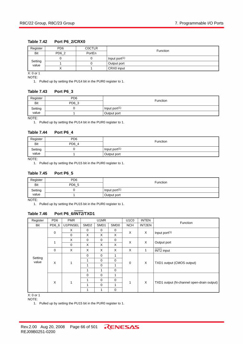
R8C/22 Group, R8C/23 Group 7. Programmable I/O Ports
Rev.2.00 Aug 20, 2008 Page 66 of 501REJ09B0251-0200
X: 0 or 1NOTE:
1. Pulled up by setting the PU14 bit in the PUR0 register to 1.
NOTE:1. Pulled up by setting the PU14 bit in the PUR0 register to 1.
NOTE:1. Pulled up by setting the PU15 bit in the PUR0 register to 1.
NOTE:1. Pulled up by setting the PU15 bit in the PUR0 register to 1.
X: 0 or 1NOTE:
1. Pulled up by setting the PU15 bit in the PUR0 register to 1.
Table 7.42 Port P6_2/CRX0Register PD6 C0CTLR
FunctionBit PD6_2 PortEn
Setting value
0 0 Input port(1)
1 0 Output portX 1 CRX0 input
Table 7.43 Port P6_3Register PD6
FunctionBit PD6_3
Setting value
0 Input port(1)
1 Output port
Table 7.44 Port P6_4Register PD6
FunctionBit PD6_4
Setting value
0 Input port(1)
1 Output port
Table 7.45 Port P6_5Register PD6
FunctionBit PD6_5
Setting value
0 Input port(1)
1 Output port
Table 7.46 Port P6_6/INT2/TXD1Register PD6 PMR U1MR U1C0 INTEN
FunctionBit PD6_6 U1PINSEL SMD2 SMD1 SMD0 NCH INT2EN
Setting value
0X 0 0 0
X X Input port(1)0 X X X
1X 0 0 0
X X Output port0 X X X
0 X X X X X 1 INT2 input
X 1
0 0 1
0 X TXD1 output (CMOS output)1 0 01 0 11 1 0
X 1
0 0 1
1 X TXD1 output (N-channel open-drain output)1 0 01 0 11 1 0

R8C/22 Group, R8C/23 Group 7. Programmable I/O Ports
Rev.2.00 Aug 20, 2008 Page 67 of 501REJ09B0251-0200
X: 0 or 1NOTE:
1. Pulled up by setting the PU15 bit in the PUR0 register to 1.
Table 7.47 Port P6_7/INT3/RXD1Register PD6 PMR INTEN
FunctionBit PD6_7 U1PINSEL INT3EN
Setting value
0 X X Input port(1)
1 X X Output port0 X 1 INT3 input0 1 X RXD1 input

R8C/22 Group, R8C/23 Group 7. Programmable I/O Ports
Rev.2.00 Aug 20, 2008 Page 68 of 501REJ09B0251-0200
7.5 Unassigned Pin HandlingTable 7.48 lists Unassigned Pin Handling.
NOTES:1. If these ports are set to output mode and left open, they remain input mode until they are switched to
output mode by a program. The voltage level of these pins may be undefined and the power current may increase while the ports remain input mode.The content of the direction registers may change due to noise or program runaway caused by noise. In order to enhance program reliability, the program should periodically repeat the setting of the direction registers.
2. Connect these unassigned pins to the MCU using the shortest wire length (2 cm or less) as possible.
3. When power-on reset function is in use.
Figure 7.13 Unassigned Pin Handling
Table 7.48 Unassigned Pin HandlingPin Name Connection
Ports P0 to P2, P3_0, P3_1, P3_3 to P3_7, P4_3 to P4_5, P6
• After setting to input mode, connect every pin to VSS via a resistor (pull-down) or connect every pin to VCC via a resistor (pull-up).(2)
• After setting to output mode, leave these pins open.(1,2)
Ports P4_6, P4_7 Connect to VCC via a resistor (pull-up)(2)
Port P4_2/VREF Connect to VCC
RESET(3) Connect to VCC via a resistor (pull-up)(2)
MCU
Port P0 to P2, P3_0,P3_1, P3_3 to P3_7,
P4_3 to P4_5, P6
(Input mode )::
(Input mode)
(Output mode)
Port P4_6, P4_7
RESET(1)
Port P4_2/VREF
::
Open
NOTE:1. When power-on reset function is in use.

R8C/22 Group, R8C/23 Group 8. Processor Mode
Rev.2.00 Aug 20, 2008 Page 69 of 501REJ09B0251-0200
8. Processor Mode
8.1 Processor ModesSingle-chip mode can be selected as processor mode.Table 8.1 lists Features of Processor Mode. Figure 8.1 shows the PM0 Register and Figure 8.2 shows the PM1Register.
Figure 8.1 PM0 Register
Figure 8.2 PM1 Register
Table 8.1 Features of Processor ModeProcessor Mode Accessible Areas Pins Assignable as I/O Port Pins
Single-chip mode SFR, internal RAM, internal ROM All pins are I/O ports or peripheralfunction I/O pins
Processor Mode Register 0(1)
Symbol Address After ResetPM0 0004h 00h
Bit Symbol Bit Name Function RW
NOTE:1.
RWReserved bits Set to 0
Set the PRC1 bit in the PRCR register to 1 (enables w riting) before rew riting to the PM0 register.
The MCU is reset w hen this bit is set to 1.When read, its content is 0. RW
—(b7-b4)
PM03Softw are reset bit
Nothing is assigned. If necessary, set to 0.When read, the content is 0.
b7 b6 b5 b4 b3 b2
—
b1 b0
0 00
—(b2-b0)
Processor Mode Register 1(1)
Symbol Address After ResetPM1 0005h 00h
Bit Symbol Bit Name Function RW
NOTES :1.2.
0
—(b1-b0) RW
Reserved bits Set to 0
b7 b6 b5 b4 b3 b2
—
b1 b0
0 0
0 : Watchdog timer interrupt1 : Watchdog timer reset(2) RW
—(b6-b3)
PM12WDT interrupt/reset sw itch bit
Nothing is assigned. If necessary, set to 0.When read, the content is 0.
The PM12 bit is set to 1 by a program (it remains unchanged even if it is set to 0).When the CSPRO bit in the CSPR register is set to 1 (selects count source protect mode), the PM12 bit isautomatically set to 1.
Reserved bit Set to 0
Set the PRC1 bit in the PRCR register to 1 (enables w riting) before rew riting to the PM1 register.
—(b7) RW

R8C/22 Group, R8C/23 Group 9. Bus
Rev.2.00 Aug 20, 2008 Page 70 of 501REJ09B0251-0200
9. BusThe bus cycles differ when accessing ROM/RAM, and when accessing SFR.Table 9.1 lists Bus Cycles by Access Space of the R8C/22 Group and Table 9.2 lists Bus Cycles by Access Space ofthe R8C/23 Group.The ROM/RAM and SFR are connected to the CPU through an 8-bit bus. When accessing in word-(16 bits) unit, thesearea are accessed twice in 8-bit unit.Table 9.3 lists Access Unit and Bus Operations.
Table 9.3 Access Unit and Bus Operations
However, only following SFRs are connected with the 16-bit bus:Timer RD: registers TRDi (i = 0, 1), TRDGRAi, TRDGRBi, TRDGRCi, and TRDGRDi Therefore, they are accessed once in 16-bit units. The bus operation is the same as “Area: SFR, data flash, even addressbyte access” in Table 9.3 Access Unit and Bus Operations, and 16-bit data is accessed at a time.
Table 9.1 Bus Cycles by Access Space of the R8C/22 GroupAccess Area Bus Cycle
SFR 2 cycles of CPU clockROM/RAM 1 cycle of CPU clock
Table 9.2 Bus Cycles by Access Space of the R8C/23 GroupAccess Area Bus Cycle
SFR/Data flash 2 cycles of CPU clockProgram ROM/RAM 1 cycle of CPU clock
Area SFR, data flash
Even addressbyte access
ROM (program ROM), RAM
Odd addressbyte access
Even addressword access
Odd addressword access
CPU clock
Data
Data
Data
Data
DataData
Data Data Data
Even Even
Odd Odd
Even + 1Even
Odd + 1Odd
Address
Even + 1
Odd + 1Odd
Data
Data
Even
Data
CPU clock
Data
Address
CPU clock
Data
Address
CPU clock
Data
Address
Data
CPU clock
Address
Data
CPU clock
Address
Data
CPU clock
Address
Data
CPU clock
Address
Data

R8C/22 Group, R8C/23 Group 10. Clock Generation Circuit
Rev.2.00 Aug 20, 2008 Page 71 of 501REJ09B0251-0200
10. Clock Generation CircuitThe clock generation circuit has:
• XIN clock oscillation circuit• Low-speed on-chip oscillator• High-speed on-chip oscillator
Table 10.1 lists Specifications of Clock Generation Circuit. Figure 10.1 shows a Clock Generation Circuit. Figures10.2 to 10.8 show clock-associated registers.
NOTES:1. These pins can be used as P4_6 and P4_7 when using the on-chip oscillator clock as the CPU
clock while the XIN clock oscillation circuit is not used.2. Set the CM05 bit in the CM0 register to 1 (main clock stops) and the CM13 bit in the CM1 register to
1 (XIN-XOUT pin) when the external clock is input.3. The clock frequency is automatically set to up to 20 MHz by a driver when using the high-speed on-
chip oscillator as the CPU clock source.
Table 10.1 Specifications of Clock Generation Circuit
Item XIN Clock Oscillation Circuit
On-Chip OscillatorHigh-Speed On-Chip Oscillator Low-Speed On-Chip Oscillator
Use of Clock • CPU clock source• Peripheral
function clock source
• CPU clock source• Peripheral function clock
source• CPU and peripheral function
clock sources when XIN clock stops oscillating
• CPU clock source• Peripheral function clock
source• CPU and peripheral function
clock sources when XIN clock stops oscillating
Clock Frequency 0 to 20 MHz Approx. 40 MHz(3) Approx. 125 kHzConnectable Oscillator
• Ceramic resonator
• Crystal oscillator
− −
Oscillator Connect Pins
XIN, XOUT(1) −(1) −(1)
Oscillation Stop, Restart Function
Usable Usable Usable
Oscillator Status After Reset
Stop Stop Oscillate
Others Externally generated clock can be input(2)
− −

R8C/22 Group, R8C/23 Group 10. Clock Generation Circuit
Rev.2.00 Aug 20, 2008 Page 72 of 501REJ09B0251-0200
Figure 10.1 Clock Generation Circuit
a
b
c
d
e
g
f1
f2
f4
f8
f32
h
k f16
S Q
R
1/2 1/2 1/2 1/2 1/2
S Q
R
FRA00
FRA01 = 1
FRA01 = 0
CM14Power-onreset
CPU clock
OCD2 = 0
OCD2 = 1
Divider
Oscillationstopdetection
XIN clock
XOUT
CM13CM05
XIN
CM02
WAITinstruction
CM10 = 1 (stop mode)
a
dc
h
b
CM06 = 0CM17 to CM16 = 11b
CM06 = 1
CM06 = 0CM17 to CM16 = 10b
CM06 = 0CM17 to CM16 = 01b
CM06 = 0CM17 to CM16 = 00b
Details of divider
Oscillation stop detection circuit
Pulse generationcircuit for clock edgedetection andcharge, dischargecontrol circuit
XIN clock
Forcible discharge when OCD0 = 0
Charge,dischargecircuit
Oscillation stop detectioninterrupt generationcircuit detection
Watchdogtimer interrupt
OCD1
OCD2 bit switch signal
CM14 bit switch signal
Oscillation stopdetection,watchdog timer, voltagemonitor 2 interrupt
CM02, CM05, CM06: Bits in CM0 registerCM10, CM13, CM14, CM16, CM17: Bits in CM1 registerOCD0, OCD1, OCD2: Bits in OCD registerFRA00, FRA01: Bits in FRA0 registerCCLK0, CCLK1, CCLK2: Bits in CCLKR register
e g
UART0A/D
converterTimer RDTimer RBTimer RA
FRA2 register
fOCO
fOCO-S
INT0
SSU/IIC
Voltage watch2 interrupt
Watchdogtimer
System clock
Low-speedon-chiposcillator
FRA1 registerFrequency adjustable
CM13
UART1
Divider
fOCO40M
On-chip oscillatorclock
fCAN0
By CCLK0,CCLK1, CCLK2
Timer RE
High-speedon-chiposcillator
fOCO-F
Divider(1/128)
fOCO128
k
Voltagedetectioncircuit
RESET
Power-on resetSoftware reset
Interrupt request

R8C/22 Group, R8C/23 Group 10. Clock Generation Circuit
Rev.2.00 Aug 20, 2008 Page 73 of 501REJ09B0251-0200
Figure 10.2 CM0 Register
System Clock Control Register 0(1)
Symbol Address After ResetCM0 0006h 01101000b
Bit Symbol Bit Name Function RW
NOTES:1.2.
3.4.
5.
b7 b6 b5 b4 b3 b2 b1 b0
0 0 1 0 0
—(b1-b0)
Reserved bits Set to 0RW
CM02
WAIT peripheral function clock stopbit
0 : Peripheral function clock does not stop in w ait mode1 : Peripheral function clock stops in w ait mode
RW
—(b3)
Reserved bit Set to 1RW
—(b4)
Reserved bit Set to 0RW
CM05XIN clock (XIN-XOUT) stop bit(2,4) 0 : XIN clock oscillates
1 : XIN clock stops(3) RW
CM06System clock division select bit 0(5) 0 : Enables CM16, CM17
1 : Divide-by-8 mode RW
—(b7)
Reserved bit Set to 0RW
When entering stop mode, the CM06 bit is set to 1 (divide-by-8 mode).
Set the PRC0 bit in the PRCR register to 1 (enables w riting) before rew riting to the CM0 register.The CM05 bit is to stop the XIN clock w hen the high-speed on-chip oscillator mode, low -speed on-chip oscillatormode is selected. Do not use this bit for w hether the XIN clock is stopped. To stop the XIN clock, set the bits in thefollow ing orders:(a) Set the OCD0 and OCD1 bits in the OCD register to 00b.(b) Set the OCD2 bit to 1 (selects on-chip oscillator clock).During external clock input, only the clock oscillation buffer is turned off and clock input is acknow ledged.P4_6 and P4_7 can be used as input ports w hen the CM05 bit is set to 1 (XIN clock stops) and the CM13 bit in theCM1 register is set to 0 (P4_6, P4_7).

R8C/22 Group, R8C/23 Group 10. Clock Generation Circuit
Rev.2.00 Aug 20, 2008 Page 74 of 501REJ09B0251-0200
Figure 10.3 CM1 Register
System Clock Control Register 1(1)
Symbol Address After ResetCM1 0007h 00100000b
Bit Symbol Bit Name Function RW
NOTES:1.2.3.4.5.
6.
7.
8.
9.
When the CM10 bit is set to 1 (stop mode) and the CM13 bit is set to 1 (XIN-XOUT pin), the XOUT(P4_7) pin becomes “H”. When the CM13 bit is set to 0 (input ports, P4_6, P4_7), the P4_7 (XOUT) entersinput mode.In count source protect mode (Refer to 13.2 Count Source Protection Mode Enabled), the value remainsunchanged even if the CM10 and CM14 bits are set.
When the CM06 bit is set to 0 (CM16, CM17 bits enabled), the CM16 to CM17 bits become enabled.If the CM10 bit is 1 (stop mode), the internal feedback resistor becomes disabled.When the OCD2 bit is set to 0 (selects XIN clock), the CM14 bit is set to 1 (stops low -speed on-chip oscillator). Whenthe OCD2 bit is set to 1 (selects on-chip oscillator clock), the CM14 bit is set to 0 (low -speed on-chip oscillator on). Itremains unchanged even if it is set to 1.When using the low voltage 2 detection interrupt (w hen using the digital f ilter), set the CM14 bit to 0 (low -speed on-chip oscillator on).
CM17 RW
b7 b6
0 0 : No division mode0 1 : Divide-by-2 mode1 0 : Divide-by-4 mode1 1 : Divide-by-16 mode
System clock division select bits 1(3)
CM16 RW
CM15XIN-XOUT drive capacity select bit(2) 0 : Low
1 : High RW
CM14Low -speed on-chip oscillation stopbit(5,6,8)
0 : Low -speed on-chip oscillator on1 : Low -speed on-chip oscillator off RW
CM13Port XIN-XOUT sw itch bit(7,9) 0 : Input ports P4_6, P4_7
1 : XIN-XOUT pin RW
—(b2-b1)
Reserved bits Set to 0RW
CM10All clock stop control bit(4,7,8) 0 : Oscillates clock
1 : Stops all clocks (stop mode) RW
b0
0 0
Once the CM13 bit is set to 1, it can not to 0 in a program.
When entering stop mode, the CM15 bit is set to 1 (drive capacity high).Set the PRC0 bit in the PRCR register to 1 (enables w riting) before rew riting to the CM1 register.
b7 b6 b5 b4 b3 b2 b1
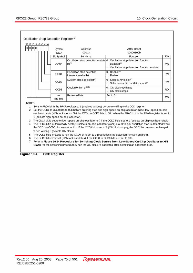
R8C/22 Group, R8C/23 Group 10. Clock Generation Circuit
Rev.2.00 Aug 20, 2008 Page 75 of 501REJ09B0251-0200
Figure 10.4 OCD Register
Oscillation Stop Detection Register(1)
Symbol Address After ResetOCD 000Ch 00000100b
Bit Symbol Bit Name Function RW
NOTES:1.2.
3.4.
5.6.7.
The OCD3 bit remains 0 (XIN clock oscillates) if the OCD1 to OCD0 bits are set to 00b.
The CM14 bit is set to 0 (low -speed on-chip oscillator on) if the OCD2 bit is set to 1 (selects on-chip oscillator clock).
Refer to Figure 10.14 Procedure for Switching Clock Source from Low-Speed On-Chip Oscillator to XINClock for the sw itching procedure w hen the XIN clock re-oscillates after detecting an oscillation stop.
Set the PRC0 bit in the PRCR register to 1 (enables w riting) before rew riting to the OCD register.
The OCD2 bit is automatically set to 1 (selects on-chip oscillator clock) if a XIN clock oscillation stop is detected w hilethe OCD1 to OCD0 bits are set to 11b. If the OCD3 bit is set to 1 (XIN clock stops), the OCD2 bit remains unchangedw hen w riting 0 (selects XIN clock).The OCD3 bit is enabled w hen the OCD0 bit is set to 1 (oscillation stop detection function enabled).
Set the OCD1 to OCD0 bits to 00b before entering stop and high-speed on-chip oscillator mode, low -speed on-chiposcillator mode (XIN clock stops). Set the OCD1 to OCD0 bits to 00b w hen the FRA01 bit in the FRA0 register is set to1 (selects high-speed on-chip oscillator).
—(b7-b4)
Reserved bits Set to 0RW
OCD3Clock monitor bit(5,6) 0 : XIN clock oscillates
1 : XIN clock stops RO
OCD2System clock select bit(4) 0 : Selects XIN clock(7)
1 : Selects on-chip oscillator clock(3) RW
OCD1 RW
OCD0 RWOscillation stop detection enablebit(7)
0 : Oscillation stop detection function disabled(2)
1 : Oscillation stop detection function enabled
0 : Disable(2)
1 : EnableOscillation stop detectioninterrupt enable bit
0 0 0 0b3 b2 b1 b0b7 b6 b5 b4

R8C/22 Group, R8C/23 Group 10. Clock Generation Circuit
Rev.2.00 Aug 20, 2008 Page 76 of 501REJ09B0251-0200
Figure 10.5 Registers FRA0 and FRA1
High-Speed On-Chip Oscillator Control Register 0(1)
Symbol Address After ResetFRA0 0023h 00h
Bit Symbol Bit Name Function RW
NOTES:1.2.
3.
Change the FRA01 bit under the follow ing conditions.• FRA00 = 1 (high-speed on-chip oscillation)• The CM14 bit in the CM1 register = 0 (low -speed on-chip oscillator on)• Bits FRA22 to FRA20 in the FRA2 register All divide ratio mode settings are supported w hen VCC = 3.0 V to 5.5 V (D, J version) 000b to 111b Divide ratio of 4 or more w hen VCC = 2.7 V to 5.5 V and K version 010b to 111bWhen setting the FRA01 bit to 0 (selects low -speed on-chip oscillator), do not set the FRA00 bit to 0 (40MHz on-chiposcillator off) at the same time.Set the FRA00 bit to 0 after setting the FRA01 bit to 0.
—(b7-b2)
Reserved bits Set to 0RW
Set the PRC0 bit in the PRCR register to 1 (enables w riting) before rew riting to the FRA0 register.
FRA00 RW
FRA01 RW
High-speed on-chip oscillator enablebit
0 : High-speed on-chip oscillator off1 : High-speed on-chip oscillator on
High-speed on-chip oscillator selectbit(2)
0 : Selects low -speed on-chip oscillator(3)
1 : Selects high-speed on-chip oscillator
0 00 0 0 0b3 b2 b1 b0b7 b6 b5 b4
High-Speed On-Chip Oscillator Control Register 1(1)
Symbol Address After ResetFRA1 0024h When Shipping
RW
NOTES:1.
2.
Set the PRC0 bit in the PRCR register to 1 (w rite enable) before rew riting to the FRA1 register.When adjusting the FRA1 register, set the value of the FRA1 register to 40 MHz and below .
RW
FunctionThe frequency of high-speed on-chip oscillator is adjusted w ith bits 0 to 7.High-speed on-chip oscillator frequency = 40 MHz (FRA1 register = value w hen shipping)Set the value of the FRA1 register to smaller, the frequency w ill be higherSet the value of the FRA1 register to larger, the frequency w ill be low er(2)
When changing the values of the FRA1 register, adjust the FRA1 register so that the frequency of the high-speedon-chip oscillator clock w ill be 40 MHz or less.
b7 b0

R8C/22 Group, R8C/23 Group 10. Clock Generation Circuit
Rev.2.00 Aug 20, 2008 Page 77 of 501REJ09B0251-0200
Figure 10.6 FRA2 Register
Figure 10.7 VCA2 Register
High-Speed On-Chip Oscillator Control Register 2(1)
Symbol Address After ResetFRA2 0025h 00h
Bit Symbol Bit Name Function RW
NOTES:1.2.3.
b7 b6 b5 b4 b3 b2 b1 b0
0 0 0 0
RW
The division of high-speed on-chiposcillator clock can be selected.b2 b1 b0
0 0 0 : Divide-by-2 mode(3)
0 0 1 : Divide-by-3 mode(3)
0 1 0 : Divide-by-4 mode0 1 1 : Divide-by-5 mode1 0 0 : Divide-by-6 mode1 0 1 : Divide-by-7 mode1 1 0 : Divide-by-8 mode1 1 1 : Divide-by-9 mode
0
FRA22 RW
High-speed on-chip oscillatorfrequency sw itching bits(2)
FRA20
Do not set on the K version products.
RW
FRA21
Set the PRC0 bit in the PRCR register to 1 (enables w riting) before rew riting to the FRA2 register.Since the value after reset is 000b, set 010b to 111b on the K version products.
—(b7-b3) RW
Reserved bits Set to 0
Voltage Detection Register 2(1)
Symbol AddressVCA2 0032h
Bit Symbol Bit Name Function RW
NOTES:1.2.
3.
4.5.
b2 b1 b0
0 0b7 b6 b5 b4 b3
When using the voltage monitor 1 reset, set the VCA26 bit to 1.After the VCA26 bit is set from 0 to 1, the voltage detection circuit elapses for td(E-A) before starting operation.
0 0 0
—(b5-b1)
Reserved bits
VCA27
After Reset(4)
Set the PRC3 bit in the PRCR register to 1 (enables w riting) before w riting to the VCA2 register.
RW
Set to 0RW
VCA26
Voltage detection 2 enable bit(3) 0 : Voltage detection 2 circuit disabled1 : Voltage detection 2 circuit enabled
RW
The LVD1ON bit in the OFS register is set to 1: 00hPower-on reset, v oltage monitor 1 reset or the LVD1ONbit in the OFS register is set to 0: 01000000b
Use the VCA20 bit only w hen entering to w ait mode. To set the VCA20 bit, follow the procedure show n in Figure10.11 Procedure for Enabling Reduced Internal Power Consumption Using VCA20 bit.
VCA20Internal pow er low consumptionenable bit(5)
0 : Disables low consumption1 : Enables low consumption RW
When using the voltage monitor 2 interrupt/reset or the VCA13 bit in the VCA1 register, set the VCA27 bit to 1.After the VCA27 bit is from 0 to 1, the voltage detection circuit elapses for td(E-A) before starting operation.The VCA27 bit remains unchanged after softw are reset, w atchdog timer reset, and voltage monitor 2 reset.
Voltage detection 1 enable bit(2) 0 : Voltage detection 1 circuit disabled1 : Voltage detection 1 circuit enabled
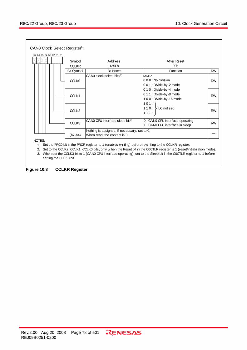
R8C/22 Group, R8C/23 Group 10. Clock Generation Circuit
Rev.2.00 Aug 20, 2008 Page 78 of 501REJ09B0251-0200
Figure 10.8 CCLKR Register
CAN0 Clock Select Register(1)
Symbol Address After ResetCCLKR 135Fh 00h
Bit Symbol Bit Name Function RW
NOTES:1.2.3.
Set to the CCLK2, CCLK1, CCLK0 bits, only w hen the Reset bit in the C0CTLR register is 1 (reset/initialization mode).When set the CCLK3 bit to 1 (CAN0 CPU interface operating), set to the Sleep bit in the C0CTLR register to 1 beforesetting the CCLK3 bit.
CCLK2 RW
—(b7-b4) —
CCLK3CAN0 CPU interface sleep bit(3) 0 : CAN0 CPU interface operating
1 : CAN0 CPU interface in sleep
CCLK0 RW
CCLK1 RW
CAN0 clock select bits(2) b2 b1 b0
0 0 0 : No division0 0 1 : Divide-by-2 mode0 1 0 : Divide-by-4 mode0 1 1 : Divide-by-8 mode1 0 0 : Divide-by-16 mode1 0 1 :1 1 0 : Do not set1 1 1 :
b0
Set the PRC0 bit in the PRCR register to 1 (enables w riting) before rew riting to the CCLKR register.
RW
Nothing is assigned. If necessary, set to 0.When read, the content is 0.
b7 b6 b5 b4 b3 b2 b1

R8C/22 Group, R8C/23 Group 10. Clock Generation Circuit
Rev.2.00 Aug 20, 2008 Page 79 of 501REJ09B0251-0200
The following describes the clocks generated by the clock generation circuit.
10.1 XIN ClockThis clock is supplied by a XIN clock oscillation circuit. This clock is used as the clock source for the CPU andperipheral function clocks. The XIN clock oscillation circuit is configured by connecting a resonator between theXIN and XOUT pins. The XIN clock oscillation circuit contains a feedback resistor, which is disconnected fromthe oscillation circuit in stop mode in order to reduce the amount of power consumed in the chip. The XIN clockoscillation circuit may also be configured by feeding an externally generated clock to the XIN pin.Figure 10.9 shows Examples of XIN Clock Connection Circuit. During or after reset, the XIN clock stops.The XIN clock starts oscillating when the CM05 bit in the CM0 register is set to 0 (XIN clock on) after setting theCM13 bit in the CM1 register to 1 (XIN- XOUT pin).To use the XIN clock for the CPU clock source, set the OCD2 bit in the OCD register to 0 (select XIN clock) afterthe XIN clock is oscillating stably.The power consumption can be reduced by setting the CM05 bit in the CM0 register to 1 (stop XIN clock) if theOCD2 bit is set to 1 (select on-chip oscillator clock).When the clocks externally generated to the XIN pin are input, a XIN clock does not stop if setting the CM05 bitto 1. If necessary, use an external circuit to stop the clock.In stop mode, all clocks including the XIN clock stop. Refer to 10.4 Power Control for details.
Figure 10.9 Examples of XIN Clock Connection Circuit
XIN XOUT
MCU(built-in feedback resistor)
Rd(1)
COUTCIN
XIN XOUT
MCU(built-in feedback resistor)
Externally derived clock
VCC
VSS
NOTE:1. Insert a damping resistor if required. The resistance will vary depending on the oscillator and the oscillation drive
capacity setting. Use the value recommended by the maker of the oscillator.Use high drive when oscillation starts and, if it is necessary to switch the oscillation drive capacity, do so afteroscillation stabilizes.When the oscillation drive capacity is set to low, check that oscillation is stable. Also, if the oscillator manufacturer'sdata sheet specifies that a feedback resistor be added external to the chip, insert a feedback resistor between XINand XOUT following the instruction.
Open
Ceramic resonator external circuit External clock input clock
Rf(1)

R8C/22 Group, R8C/23 Group 10. Clock Generation Circuit
Rev.2.00 Aug 20, 2008 Page 80 of 501REJ09B0251-0200
10.2 On-Chip Oscillator ClocksThis clock is supplied by an on-chip oscillator. The on-chip oscillator contains a high-speed on-chip oscillator anda low-speed on-chip oscillator. Either an on-chip oscillator clock is selected by the FRA01 bit in the FRA0 register.
10.2.1 Low-Speed On-Chip Oscillator ClockThe clock generated by the low-speed on-chip oscillator is used as the clock source for the CPU clock,peripheral function clock, fOCO, and fOCO-S.After reset, the on-chip oscillator clock generated by the low-speed on-chip oscillator by divide-by-8 isselected for the CPU clock.If the XIN clock stops oscillating when the OCD1 to OCD0 bits in the OCD register are set to 11b, the low-speed on-chip oscillator automatically starts operating, supplying the necessary clock for the MCU.The frequency of the low-speed on-chip oscillator varies depending on the supply voltage and the operatingambient temperature. The application products must be designed with sufficient margin to accommodate thefrequency range.
10.2.2 High-Speed On-Chip Oscillator ClockThe clock generated by the high-speed on-chip oscillator is used as the clock source for the CPU clock,peripheral function clock, fOCO, fOCO-F and fOCO40M.To use the high-speed on-chip oscillator clock as the clock source of the CPU clock, peripheral clock, fOCO,and fOCO-F, set bits FRA20 to FRA22 in the FRA2 register as follows;All divide ratio mode settings are supported when VCC = 3.0 V to 5.5 V (D, J version)000b to 111bDivide ratio of 4 or more when VCC = 2.7 V to 5.5 V and K version 010b to 111b After reset, the on-chip oscillator clock generated by the high-speed on-chip oscillator stops. The oscillationstarts by setting the FRA00 bit in the FRA0 register to 1 (high-speed on-chip oscillator on). The frequency canbe adjusted by the FRA1 and FRA2 registers.Since there are differences in the amount of frequency adjustment among the bits in the FRA1 register, makeadjustments by changing the settings of individual bits.Adjust the amount of high-speed on-chip oscillator frequency to 40 MHz and below by setting the FRA1register.

R8C/22 Group, R8C/23 Group 10. Clock Generation Circuit
Rev.2.00 Aug 20, 2008 Page 81 of 501REJ09B0251-0200
10.3 CPU Clock and Peripheral Function ClockThere are two type clocks: a CPU clock to operate the CPU and a peripheral function clock to operate theperipheral functions. Refer to Figure 10.1 Clock Generation Circuit.
10.3.1 System ClockThe system clock is a clock source for the CPU and peripheral function clocks. The XIN clock or on-chiposcillator clock can be selected.
10.3.2 CPU ClockThe CPU clock is an operating clock for the CPU and watchdog timer.The system clock can be the divide-by-1 (no division), 2, 4, 8 or 16 to produce the CPU clock. Use the CM06bit in the CM0 register and the CM16 to CM17 bits in the CM1 register to select the value of the division.After reset, the low-speed on-chip oscillator clock divided-by-8 provides the CPU clock.When entering stop mode, the CM06 bit is set to 1 (divide-by-8 mode).
10.3.3 Peripheral Function Clock (f1, f2, f4, f8, f32, and fCAN0)The peripheral function clock is operating clock for the peripheral functions.The clock fi (i = 1, 2, 4, 8, 32) is generated by the system clock divided-by-i. The clock fi is used for timersRA, RB, RD, RE, serial interface, A/D converter and CAN module.The clock fCAN0 is generated by the f1 clock divided-by-1(no-division), -2, -4, -8, or -16, and is used for CANmodule.When the WAIT instruction is executed after setting the CM02 bit in the CM0 register to 1 (peripheral functionclock stops in wait mode), the clock fi and fCAN0 stop.(1)
NOTE:1. fCAN0 clock stops at high level in CAN0 sleep mode.
10.3.4 fOCOfOCO is operating clocks for the peripheral functions.The fOCO run at the same frequency as the on-chip oscillator clock and can be used as the source for the timerRA.When the WAIT instruction is executed, the clocks fOCO does not stop.
10.3.5 fOCO40MfOCO40M is used as the count source for the timer RD. The fOCO40M is generated by the high-speed on-chiposcillator and provided by setting the FRA00 bit to 1.When the WAIT instruction is executed, the clock fOCO40M does not stop.fOCO40M can be used with supply voltage VCC = 3.0 to 5.5V.
10.3.6 fOCO-FfOCO-F is used as the count source for the AD converter. The fOCO-F is generated by the high-speed on-chiposcillator and provided by setting the FRA00 bit to 1.When the WAIT instruction is executed, the clock fOCO-F does not stop.
10.3.7 fOCO-SfOCO-S is an operating clock for the watchdog timer and voltage detection circuit. When setting the CM14 bitto 0 (low-speed on-chip oscillator on) using the clock generated by the low-speed on-chip oscillator, the fOCO-S can be provided. When the WAIT instruction is executed or in count source protect mode of the watchdogtimer, the clock fOCO-S does not stop.

R8C/22 Group, R8C/23 Group 10. Clock Generation Circuit
Rev.2.00 Aug 20, 2008 Page 82 of 501REJ09B0251-0200
10.3.8 fOCO128fOCO128 is generated by fOCO divided-by-128. The clock fOCO128 is used for capture signal of timer RD(channel 0).

R8C/22 Group, R8C/23 Group 10. Clock Generation Circuit
Rev.2.00 Aug 20, 2008 Page 83 of 501REJ09B0251-0200
10.4 Power ControlThere are three power control modes. All modes other than wait and stop modes are referred to as standardoperating mode.
10.4.1 Standard Operating ModeStandard operating mode is further separated into three modes.In standard operating mode, the CPU clock and the peripheral function clock are supplied to operate the CPUand the peripheral function clocks. Power consumption control is enabled by controlling the CPU clockfrequency. The higher the CPU clock frequency, the more processing power increases. The lower the CPUclock frequency, the more power consumption decreases. When unnecessary oscillator circuits stop, powerconsumption is further reduced.Before the clock sources for the CPU clock can be switched over, the new clock source after switching needs tobe stabilized and oscillated. If the new clock source is the XIN clock, allow sufficient wait time in a programuntil an oscillation is stabilized before exiting.
−: can be 0 or 1, no change in outcome.
10.4.1.1 High-Speed Clock ModeThe XIN clock divided-by-1 (no division), -2, -4, -8, or -16 provides the CPU clock. Set the CM06 bit to 1(divide-by-8 mode) when transiting to high-speed on-chip oscillator mode, low-speed on-chip oscillator mode.If the CM14 bit is set to 0 (low-speed on-chip oscillator on) or the FRA00 bit in the FRA0 register is set to 1(high-speed on-chip oscillator on), the fOCO can be used for timers RA.When the FRA00 bit is set to 1, fOCO40M can be used for timer RD.When the CM14 bit is set to 0 (low-speed on-chip oscillator on), fOCO-S can be used for the watchdog timerand voltage detection circuit.
10.4.1.2 High-Speed On-Chip Oscillator ModeThe high-speed on-chip oscillator is used as the on-chip oscillator clock when the FRA00 bit in the FRA0register is set to 1 (high-speed on-chip oscillator on) and the FRA01 bit in the FRA0 register is set to 1. The on-chip oscillator divided-by-1 (no division), -2, -4, -8 or -16 provides the CPU clock. Set the CM06 bit to 1(divide-by-8) when transiting to high-speed clock mode. If the FRA00 bit is set to 1, fOCO40M can be used for timer RD.When the CM14 bit is set to 0 (low-speed on-chip oscillator on), fOCO-S can be used for the watchdog timerand voltage detection circuit.
Table 10.2 Settings and Modes of Clock Associated Bits
ModesOCD Register CM1 Register CM0 Register FRA0 Register
OCD2 CM17, CM16 CM14 CM13 CM06 CM05 FRA01 FRA00High-speed clock mode
No division 0 00b − 1 0 0 − −Divide-by-2 0 01b − 1 0 0 − −Divide-by-4 0 10b − 1 0 0 − −Divide-by-8 0 − − 1 1 0 − −Divide-by-16 0 11b − 1 0 0 − −
High-speed on-chip oscillator mode
No division 1 00b − − 0 − 1 1Divide-by-2 1 01b − − 0 − 1 1Divide-by-4 1 10b − − 0 − 1 1Divide-by-8 1 − − − 1 − 1 1Divide-by-16 1 11b − − 0 − 1 1
Low-speed on-chip oscillator mode
No division 1 00b 0 − 0 − 0 −Divide-by-2 1 01b 0 − 0 − 0 −Divide-by-4 1 10b 0 − 0 − 0 −Divide-by-8 1 − 0 − 1 − 0 −Divide-by-16 1 11b 0 − 0 − 0 −

R8C/22 Group, R8C/23 Group 10. Clock Generation Circuit
Rev.2.00 Aug 20, 2008 Page 84 of 501REJ09B0251-0200
10.4.1.3 Low-Speed On-Chip Oscillator ModeIf the CM14 bit in the CM1 register is set to 0 (low-speed on-chip oscillator on) or the FRA01bit in the FRA0register is set to 0, the low-speed on-chip oscillator provides the on-chip oscillator clock.The on-chip oscillator clock divided-by-1 (no division), -2, -4, -8 or -16 provides the CPU clock. The on-chiposcillator clock is also the clock source for the peripheral function clocks. Set the CM06 bit to 1 (divide-by-8mode) when transiting to high-speed clock mode. When the FRA00 bit is set to 1, fOCO40M can be used fortimer RD. When the CM14 bit is set to 0 (low-speed on-chip oscillator on), fOCO-S can be used for thewatchdog timer and voltage detection circuit.In this mode, stopping the XIN clock and high-speed on-chip oscillator, and setting the FMR47 bit in theFMR4 register to 1 (flash memory low consumption current read mode enabled) enables low consumptionoperation. To enter wait mode from low-speed on-chip oscillator mode, setting the VCA20 bit in the VCA2 register to 1(internal power low consumption enabled) enables lower consumption current in wait mode.When enabling reduced internal power consumption using the VCA20 bit, follow Figure 10.11 Procedure forEnabling Reduced Internal Power Consumption Using VCA20 bit.
10.4.2 Wait ModeSince the CPU clock stops in wait mode, the CPU operated in the CPU clock and the watchdog timer whencount source protection mode is disabled stops. The XIN clock and on-chip oscillator clock do not stop and theperipheral functions using these clocks maintain operating.
10.4.2.1 Peripheral Function Clock Stop FunctionIf the CM02 bit is set to 1 (peripheral function clock stops in wait mode), the f1, f2, f4, f8, f32, and fCAN0clocks stop in wait mode. The power consumption can be reduced.
10.4.2.2 Entering Wait ModeThe MCU enters wait mode when the WAIT instruction is executed.When the OCD2 bit in the OCD register is set to 1 (on-chip oscillator selected as system clock), set theOCD1bit in the OCD register to 0 (oscillation stop detection interrupt disabled) before executing the WAITinstruction.If the MCU enters wait mode while the OCD1 bit is set to 1 (oscillation stop detection interrupt enabled),current consumption is not reduced because the CPU clock does not stop.
10.4.2.3 Pin Status in Wait ModeThe I/O port is the status before wait mode was entered is maintained.

R8C/22 Group, R8C/23 Group 10. Clock Generation Circuit
Rev.2.00 Aug 20, 2008 Page 85 of 501REJ09B0251-0200
10.4.2.4 Exiting Wait ModeThe MCU exits wait mode by a hardware reset or peripheral function interrupt. When using a hardware reset toexit wait mode, set the ILVL2 to ILVL0 bits for the peripheral function interrupts to 000b (interrupts disabled)before executing the WAIT instruction.The peripheral function interrupts are affected by the CM02 bit. When the CM02 bit is set to 0 (peripheralfunction clock does not stop in wait mode), all peripheral function interrupts can be used to exit wait mode.When the CM02 bit is set to 1 (peripheral function clock stops in wait mode), the peripheral functions using theperipheral function clock stop operating and the peripheral functions operated by external signals can be usedto exit wait mode.Table 10.3 lists Interrupts to Exit Wait Mode and Usage Conditions.
Figure 10.10 shows the Time from Wait Mode to Interrupt Routine Execution.When using a peripheral function interrupt to exit wait mode, set up the following before executing the WAITinstruction.
(1) Set the interrupt priority level to the ILVL2 to ILVL0 bits in the interrupt control register of theperipheral function interrupts to use for exiting wait mode. Set the ILVL2 to ILVL0 bits of theperipheral function interrupts not to use for exiting wait mode to 000b (disables interrupt).
(2) Set the I flag to 1.(3) Operate the peripheral function to use for exiting wait mode.
When exiting by a peripheral function interrupt, the time (number of cycles) between interrupt requestgeneration and interrupt routine execution is determined by the settings of the FMSTP bit in the FMR0 registeras described in Figure 10.10.The CPU clock, when exiting wait mode by a peripheral function interrupt, is the same clock as the CPU clockwhen the WAIT instruction is executed.
Table 10.3 Interrupts to Exit Wait Mode and Usage ConditionsInterrupt CM02 = 0 CM02 = 1
Serial Interface Interrupt Usable when operating with internal or external clock
Usable when operating with external clock
Clock Synchronous Serial I/O with Chip Select Interrupt / I2C Bus Interface Interrupt
Usable in all modes − (Do not use)
Key Input Interrupt Usable UsableA/D Conversion Interrupt Usable in one-shot mode − (Do not use)Timer RA Interrupt Usable in all modes Can be used if there is no filter in event
counter mode.Usable by selecting fOCO as count source.
Timer RB Interrupt Usable in all modes − (Do not use)Timer RD Interrupt Usable in all modes Usable by selecting fOCO40M as
count sourceTimer RE Interrupt Usable in all modes − (Do not use)INT Interrupt Usable Usable (INT0 to INT3 can be used if
there is no filter.)Voltage Monitor 2 Interrupt Usable UsableOscillation Stop Detection Interrupt
Usable − (Do not use)
CAN0 Wake-Up Interrupt Usable in CAN sleep mode Usable in CAN sleep mode

R8C/22 Group, R8C/23 Group 10. Clock Generation Circuit
Rev.2.00 Aug 20, 2008 Page 86 of 501REJ09B0251-0200
Figure 10.10 Time from Wait Mode to Interrupt Routine Execution
FMR0 RegisterFMSTP Bit
Time until Flash Memory isActivated (T1)
Time until CPU Clock isSupplied (T2)
Time for InterruptSequence (T3) Remarks
0(flash memory
operates)
Period of system clock× 12 cycles + 30 µs (max.)
Period of CPU clock× 6 cycles
Period of CPU clock× 20 cycles
Following totaltime is the timefrom wait modeuntil an interruptroutine isexecuted.
1(flash memory
stops)
Period of system clock× 12 cycles Same as above Same as above
Wait mode Flash memory activationsequence
CPU clock restartsequence Interrupt sequence
T1 T2 T3
Interrupt request generated

R8C/22 Group, R8C/23 Group 10. Clock Generation Circuit
Rev.2.00 Aug 20, 2008 Page 87 of 501REJ09B0251-0200
10.4.2.5 Reducing Internal Power ConsumptionInternal power consumption can be reduced by using low-speed on-chip oscillator mode.Figure 10.11 shows the Procedure for Enabling Reduced Internal Power Consumption Using VCA20 bit.When enabling reduced internal power consumption using the VCA20 bit, follow Figure 10.11 Procedure forEnabling Reduced Internal Power Consumption Using VCA20 bit.
Figure 10.11 Procedure for Enabling Reduced Internal Power Consumption Using VCA20 bit
NOTES:1. Execute this handling to all interrupt handlings generated around the WAIT instruction. If it is not necessary to start the high-speed
clock or the high-speed on-chip oscillator in the interrupt handling, it does not need to be started.2. Do not set the VCA20 bit to 0 with the instruction immediately after setting the VCA20 bit to 1. Also, do not do the opposite.3. When the VCA20 bit is set to 1, do not set the CM10 bit to 1 (stop mode).4. When entering wait mode, follow 10.6.2 Wait Mode.
Handling procedure of internal powerlow consumption enabled by VCA20 bit
Enter low-speed on-chip oscillator mode
Stop XIN clock and high-speed on-chiposcillator clock
VCA20 ← 1 (internal power low consumptionenabled)(2)
Enter wait mode(4)
VCA20 ← 0 (internal power low consumptiondisabled)(2)
Start XIN clock or high-speed on-chiposcillator clock
(Wait until XIN clock oscillation stabilizes)
Enter high-speed clock mode or high-speedon-chip oscillator mode
In interrupt handling routine
VCA20 ← 0 (internal power low consumptiondisabled)(2)
Start XIN clock or high-speed on-chiposcillator clock
Enter high-speed clock mode or high-speedon-chip oscillator mode
Enter low-speed on-chip oscillator mode
Exit wait mode byinterrupt
Stop XIN clock and high-speed on-chiposcillator clock
VCA20 ← 1 (internal power low consumptionenabled)(2,3)
Interrupt handling completed
Step (1)
Step (2)
Step (3)
Step (4)
Step (5)
Step (6)
Step (7)
Step (8)
Step (5)
Step (6)
Step (7)
Step (8)
(Wait until XIN clock oscillation stabilizes)
Step (1)
Step (2)
Step (3)
If it is necessary to startthe high-speed clock orthe high-speed on-chiposcillator in the interrupthandling routine, executesteps (5) to (7) in theinterrupt routine.
If the high-speed clock orhigh-speed on-chiposcillator is started in theinterrupt handling routine,execute steps (1) to (3) atthe last of the interruptroutine.
(Note 1)
Interrupt handling
VCA20: Bit in VCA2 register

R8C/22 Group, R8C/23 Group 10. Clock Generation Circuit
Rev.2.00 Aug 20, 2008 Page 88 of 501REJ09B0251-0200
10.4.3 Stop ModeSince the oscillator circuits stop in wait mode, the CPU clock and peripheral function clock stop and the CPUand peripheral functions clocked by these clocks stop operating. The least power required to operate the MCUis in stop mode. If the voltage applied to the VCC pin is VRAM or more, the internal RAM is maintained.The peripheral functions clocked by external signals maintain operating.Table 10.4 lists Interrupts to Exit Stop Mode and Usage Conditions.
10.4.3.1 Entering Stop ModeThe MCU enters stop mode by setting the CM10 bit in the CM1 register to 1 (all clocks stop). At the sametime, the CM06 bit in the CM0 register is set to 1 (divide-by-8 mode) and the CM15 bit in the CM10 register isset to 1 (drive capability HIGH of XIN clock oscillator circuit).When using stop mode, set the OCD1 to OCD0 bits to 00b before entering stop mode.
10.4.3.2 Pin Status in Stop ModeThe status before entering wait mode is maintained.However, when the CM13 bit in the CM1 register is set to 1 (XIN-XOUT pins), the XOUT(P4_7) pin is held“H”. When the CM13 bit is set to 0 (input port P4_6 and P4_7), the P4_7(XOUT) is held in input status.
10.4.3.3 Exiting Stop ModeThe MCU exits stop mode by a reset or peripheral function interrupt.When using a reset to exit stop mode, set the ILVL2 to ILVL0 bits for the peripheral function interrupts to 000b(disables interrupts) before setting the CM10 bit to 1.Figure 10.12 shows the Time from Stop Mode to Interrupt Routine Execution.When using a peripheral function interrupt to exit stop mode, set up the following before setting the CM10 bitto 1.
(1) Set the interrupt priority level to the ILVL2 to ILVL0 bits of the peripheral function interrupts to use forexiting stop mode. Set the ILVL2 to ILVL0 bits of the peripheral function interrupts not to use forexiting stop mode to 000b (disables interrupt).
(2) Set the I flag to 1.(3) Operates the peripheral function to use for exiting stop mode.
When exiting by a peripheral function interrupt, the interrupt sequence is executed when an interruptrequest is generated and the CPU clock supply is started.
If the clock used immediately before stop mode is a system clock and stop mode is exited by a peripheralfunction interrupt, the CPU clock becomes the previous system clock divided by 8.
Table 10.4 Interrupts to Exit Stop Mode and Usage ConditionsInterrupt Usage Conditions
Key Input Interrupt −
INT0 to INT3 Interrupt Can be used if there is no filterTimer RA Interrupt When there is no filter and external pulse is counted in event
counter modeSerial Interface Interrupt When external clock is selectedVoltage Monitor 2 Interrupt Usable in digital filter disabled mode (VW2C1 bit in VW2C register
is set to 1)CAN0 Wake-Up Interrupt Usable in CAN sleep mode

R8C/22 Group, R8C/23 Group 10. Clock Generation Circuit
Rev.2.00 Aug 20, 2008 Page 89 of 501REJ09B0251-0200
Figure 10.12 Time from Stop Mode to Interrupt Routine Execution
Time until Flash Memory isActivated (T2)
Time until CPU Clock isSupplied (T3)
Time for InterruptSequence (T4) Remarks
0(flash memory
operates)
Period of system clock× 12 cycles + 30 µs (max.)
Period of CPU clock× 6 cycles
Period of CPU clock× 20 cycles
Following totaltime of T0 to T4 isthe time from waitmode until aninterrupt routine isexecuted.
1(flash memory
stops)
Period of system clock× 12 cycles Same as above Same as above
Stopmode
Flash memory activationsequence
CPU clock restartsequence Interrupt sequence
T2 T3 T4
Interruptrequest
generated
Oscillation period of the CPUclock source used immediately
before stop mode
T1
Internalpower
stability time
150 µs(max.)
T0
FMR0 RegisterFMSTP Bit

R8C/22 Group, R8C/23 Group 10. Clock Generation Circuit
Rev.2.00 Aug 20, 2008 Page 90 of 501REJ09B0251-0200
Figure 10.13 shows the State Transitions in Power Control Mode.
Figure 10.13 State Transitions in Power Control Mode
CM10 = 1
CPU operation stops
Stop mode
Reset
Wait mode
Low-speed on-chip oscillator modeCM14 = 0OCD2 = 1FRA01 = 0
High-speed on-chip oscillator modeOCD2 = 1FRA00 = 1FRA01 = 1
High-speed clock modeCM05 = 0CM13 = 1OCD2 = 0
Standard operating mode
CM14 = 0OCD2 = 1FRA01 = 0
CM05 = 0CM13 = 1OCD2 = 0
CM05 = 0CM13 = 1OCD2 = 0
OCD2 = 1FRA00 = 1FRA01 = 1
FRA00 = 1FRA01 = 1
CM14 = 0FRA01 = 0
All oscillators stop
InterruptWAIT instructionInterrupt
CM05 : CM0 registerCM13, CM14 : CM1 registerOCD2 : OCD registerFRA00, FRA01 : FRA0 register
State Transition in Power Control Mode

R8C/22 Group, R8C/23 Group 10. Clock Generation Circuit
Rev.2.00 Aug 20, 2008 Page 91 of 501REJ09B0251-0200
10.5 Oscillation Stop Detection FunctionThe oscillation stop detection function is a function to detect the stop of the XIN clock oscillating circuit. Theoscillation stop detection function can be enabled and disabled by the OCD0 bit in the OCD register.Table 10.5 lists the Specifications of Oscillation Stop Detection Function.
When the XIN clock is the CPU clock source and the OCD1 to OCD0 bits are set to 11b, the system is placed inthe following state if the XIN clock stops.
• OCD2 bit in OCD register = 1 (on-chip oscillator clock selected)• OCD3 bit in OCD register = 1 (XIN clock stops)• CM14 bit in CM1 register = 0 (low-speed on-chip oscillator oscillates)• Oscillation stop detection interrupt request is generated
10.5.1 How to Use Oscillation Stop Detection Function• The oscillation stop detection interrupt shares the vector with the voltage monitor 2 interrupt and the
watchdog timer interrupt. When using the oscillation stop detection interrupt and watchdog timer interrupt,the interrupt cause needs to be determined.Table 10.6 lists the Determining Interrupt Source for Oscillation Stop Detection, Watchdog Timer, VoltageMonitor 1, and Voltage Monitor 2 Interrupts.Figure 10.15 shows an Example of Determining Interrupt Source for Oscillation Stop Detection, WatchdogTimer, Voltage Monitor 1, or Voltage Monitor 2 Interrupt.
• When the XIN clock is re-oscillated after oscillation stop, switch the XIN clock to the clock source of theCPU clock and peripheral functions by a program.Figure 10.14 shows the Procedure for Switching Clock Source from Low-Speed On-Chip Oscillator toXIN Clock.
• To enter wait mode while using the oscillation stop detection function, set the CM02 bit to 0 (peripheralfunction clock does not stop in wait mode).
• Since the oscillation stop detection function is a function preparing to stop the XIN clock by the externalcause, set the OCD1 to OCD0 bits to 00b when the XIN clock stops or oscillates in the program, that is stopmode is selected or the CM05 bit is changed.
• This function cannot be used when the XIN clock frequency is less than 2 MHz. Set the OCD1 to OCD0bits to 00b.
• When using the low-speed on-chip oscillator clock for the CPU clock and clock sources of peripheralfunctions after detecting the oscillation stop, set the FRA01 bit in the FRA0 register to 0 (low-speed on-chip oscillator selected) and the OCD1 to OCD0 bits to 11b. When using the high-speed on-chip oscillator clock for the CPU clock and clock sources of peripheralfunctions after detecting the oscillation stop, set the FRA00 bit to 1 (high-speed on-chip oscillator on) andthe FRA01 bit to 1 (high-speed on-chip oscillator selected) and the OCD1 to OCD0 bits to 11b.
Table 10.5 Specifications of Oscillation Stop Detection FunctionItem Specification
Oscillation Stop Detection Clock and Frequency Bandwidth
f(XIN) ≥ 2 MHz
Enabled Condition for Oscillation Stop Detection Function
Set OCD1 to OCD0 bits to 11b
Operation at Oscillation Stop Detection Oscillation stop detection interrupt is generated

R8C/22 Group, R8C/23 Group 10. Clock Generation Circuit
Rev.2.00 Aug 20, 2008 Page 92 of 501REJ09B0251-0200
Figure 10.14 Procedure for Switching Clock Source from Low-Speed On-Chip Oscillator to XIN Clock
Table 10.6 Determining Interrupt Source for Oscillation Stop Detection, Watchdog Timer, Voltage Monitor 1, and Voltage Monitor 2 Interrupts
Generated Interrupt Source Bit Showing Interrupt CauseOscillation Stop Detection((a) or (b))
(a) OCD3 bit in OCD register = 1(b) OCD1 to OCD0 bits in OCD register = 11b and the OCD2 bit = 1
Watchdog Timer VW2C3 bit in VW2C register = 1Voltage Monitor 2 VW2C2 bit in VW2C register = 1
Set OCD1 to OCD0 bits to 00b
Determine several timesthat the OCD bit is 0 (XIN clock
oscillates)
Yes
Set OCD2 bit to 0(select XIN Clock)
End
Switch to XIN clock
OCD3 to OCD0 bits: Bits in OCD register
No

R8C/22 Group, R8C/23 Group 10. Clock Generation Circuit
Rev.2.00 Aug 20, 2008 Page 93 of 501REJ09B0251-0200
Figure 10.15 Example of Determining Interrupt Source for Oscillation Stop Detection, Watchdog Timer, Voltage Monitor 1, or Voltage Monitor 2 Interrupt
NOTE:1. This disables multiple oscillation stop detection interrupts.
OCD1 to OCD3: Bits in OCD registerVW2C3: Bit in VW2C register
Interrupt sources judgment
OCD3 = 1?(XIN clock stops)
OCD1 = 1 (Oscillationstop detection interrupt enable), and
OCD2 = 1 (Selects on-chiposcillator clock)?
VW2C3 = 1?(Watchdog time underflows)
Jump to oscillation stop detectioninterrupt process routine.
Jump to voltage monitor 2 Interruptprocess routine.
Jump to watchdog timer interruptprocess routine.
NO
YES
NO
YES
NO
YES
OCD1 = 0 (Oscillation stop detectioninterrupt disable) (1)

R8C/22 Group, R8C/23 Group 10. Clock Generation Circuit
Rev.2.00 Aug 20, 2008 Page 94 of 501REJ09B0251-0200
10.6 Notes on Clock Generation Circuit
10.6.1 Stop ModeWhen entering stop mode, set the FMR01 bit to “0” (CPU rewrite mode disabled) and the CM10 bit to “1” (stopmode). An instruction queue pre-reads 4 bytes from the instruction which sets the CM10 bit in the CM1 registerto “1” (stop mode) and the program stops. Insert at least 4 NOP instructions following the JMP.B instructionafter the instruction which sets the CM10 bit to “1”.
• Example to enter stop modeBCLR 1,FMR0 ; CPU rewrite mode disabledBSET 0,PRCR ; Protect disabledFSET I ; Enable interruptBSET 0,CM1 ; Stop modeJMP.B LABEL_001
LABEL_001:NOPNOPNOPNOP
10.6.2 Wait ModeWhen entering wait mode, set the FMR01 bit to “0” (CPU rewrite mode disabled) and execute the WAITinstruction. An instruction queue pre-reads 4 bytes from the WAIT instruction and the program stops. Insert atleast 4 NOP instructions after the WAIT instruction.
• Example to execute the WAIT instructionBCLR 1,FMR0 ; CPU rewrite mode disabledFSET I ; Enable interruptWAIT ; Wait modeNOPNOPNOPNOP
10.6.3 Oscillation Stop Detection FunctionSince the oscillation stop detection function cannot be used if the XIN clock frequency is less than 2 MHz, setthe OCD1 to OCD0 bits to 00b.
10.6.4 Oscillation Circuit ConstantsAsk the maker of the oscillator to specify the beat oscillation circuit constants on your system.

R8C/22 Group, R8C/23 Group 11. Protection
Rev.2.00 Aug 20, 2008 Page 95 of 501REJ09B0251-0200
11. ProtectionProtection function protects important registers from being easily overwritten when a program runs out of control.Figure 11.1 shows the PRCR Register. The following lists the registers protected by the PRCR register.
• Registers protected by PRC0 bit: CM0, CM1, OCD, FRA0, FRA1, FRA2, and CCLKR registers• Registers protected by PRC1 bit: PM0 and PM1 registers• Registers protected by PRC2 bit: PD0 register• Registers protected by PRC3 bit: VCA2, VW1C and VW2C registers
Figure 11.1 PRCR Register
Protect Register
Symbol Address After ResetPRCR 000Ah 00h
Bit Symbol Bit Name Function RW
NOTE:1.
PRC2Protect bit 2 Writing to the PD0 register is enabled
0 : Disables w riting1 : Enables w riting(1)
RW
PRC0 RW
PRC1 RW
Protect bit 0 Writing to the CM0, CM, OCD, FRA0, FRA1, FRA2,and CCLKR registers is enabled0 : Disables w riting1 : Enables w riting
Protect bit 1 Writing to the PM0 and PM1 registers is enabled0 : Disables w riting1 : Enables w riting
0 0b3 b2 b1 b0b7 b6 b5 b4
RW
—(b5-b4)
Reserved bits Set to 0RW
PRC3
Protect bit 3 Writing to the VCA2, VW1C and VW2C registers isenabled0 : Disables w riting1 : Enables w riting
This bit is set to 0 after w riting 1 to the PRC2 bit and executing w riting to any address.Since the other bits are not set to 0, set to 0 by a program.
—(b7-b6)
Reserved bits When read, the content is 0.RO

R8C/22 Group, R8C/23 Group 12. Interrupts
Rev.2.00 Aug 20, 2008 Page 96 of 501REJ09B0251-0200
12. Interrupts
12.1 Interrupt Overview
12.1.1 Types of InterruptsFigure 12.1 shows the Interrupts.
Figure 12.1 Interrupts
• Maskable interrupt: The interrupt enable flag (I flag) enables or disables these interrupt. Theinterrupt priority order can be changed based on the interrupt priority level.
• Non-maskable interrupt: The interrupt enable flag (I flag) does not enable or disable an interrupt. Theinterrupt priority order based on interrupt priority level cannot be changed.
Interrupt
(non-maskable interrupt)
Hardware
Software
(non-maskable interrupt)
(maskable interrupt)
Special
Peripheral function(1)
Undefined instruction (UND instruction)Overflow (INTO instruction)BRK instructionINT instruction
Watchdog timerOscillation stop detectionVoltage monitor 2Single step(2)
Address break(2)
Address match
NOTES: 1. Peripheral function interrupts in the MCU are used to generate the peripheral interrupt. 2. Do not use this interrupt. This is for use with development tools only.

R8C/22 Group, R8C/23 Group 12. Interrupts
Rev.2.00 Aug 20, 2008 Page 97 of 501REJ09B0251-0200
12.1.2 Software InterruptsA software interrupt is generated when an instruction is executed. The software interrupts are non-maskableinterrupts.
12.1.2.1 Undefined Instruction InterruptThe undefined instruction interrupt is generated when the UND instruction is executed.
12.1.2.2 Overflow InterruptThe overflow interrupt is generated when the O flag is set to 1 (arithmetic operation overflow) and the INTOinstruction is executed. Instructions to set the O flag are:ABS, ADC, ADCF, ADD, CMP, DIV, DIVU, DIVX, NEG, RMPA, SBB, SHA, SUB
12.1.2.3 BRK InterruptA BRK interrupt is generated when the BRK instruction is executed.
12.1.2.4 INT Instruction InterruptAn INT instruction interrupt is generated when the INT instruction is executed. The INT instruction can selectsoftware interrupt numbers 0 to 63. Software interrupt numbers 3 to 31 are assigned to the peripheral functioninterrupt. Therefore, the MCU executes the same interrupt routine when the INT instruction is executed aswhen a peripheral function interrupt is generated. In software interrupt numbers 0 to 31, the U flag is saved tothe stack during instruction execution and set the U flag to 0 (ISP selected) before executing an interruptsequence. The U flag is restored from the stack when returning from the interrupt routine. In software interruptnumbers 32 to 63, the U flag does not change state during instruction execution, and the selected SP is used.

R8C/22 Group, R8C/23 Group 12. Interrupts
Rev.2.00 Aug 20, 2008 Page 98 of 501REJ09B0251-0200
12.1.3 Special InterruptsSpecial interrupts are non-maskable interrupts.
12.1.3.1 Watchdog Timer InterruptThe watchdog timer interrupt is generated by the watchdog timer. For details, refer to 13. Watchdog Timer.
12.1.3.2 Oscillation Stop Detection InterruptOscillation Stop Detection Interrupt is generated by the oscillation stop detection function. For details of theoscillation stop detection function, refer to 10. Clock Generation Circuit.
12.1.3.3 Voltage Monitor 2 InterruptThe voltage monitor 2 interrupt is generated by the voltage detection circuit. For details of the voltagedetection circuit, refer to 6. Voltage Detection Circuit.
12.1.3.4 Single-Step Interrupt, and Address Break InterruptDo not use the single-step interrupt. For development tools only.
12.1.3.5 Address Match InterruptThe address match interrupt is generated immediately before executing an instruction that is stored into anaddress indicated by the RMAD0 to RMAD1 registers when the AIER0 or AIER1 bit in the AIER registerwhich is set to 1 (address match interrupt enable).For details of the address match interrupt, refer to 12.5 Address Match Interrupt.
12.1.4 Peripheral Function InterruptThe peripheral function interrupt is generated by the internal peripheral function of the MCU and a maskableinterrupt. Refer to Table 12.2 Relocatable Vector Tables for sources of the peripheral function interrupt. Fordetails of the peripheral function, refer to the description of each peripheral function.

R8C/22 Group, R8C/23 Group 12. Interrupts
Rev.2.00 Aug 20, 2008 Page 99 of 501REJ09B0251-0200
12.1.5 Interrupts and Interrupt VectorThere are 4 bytes in one vector. Set the starting address of interrupt routine in each vector table. When aninterrupt request is acknowledged, the CPU branches to the address set in the corresponding interrupt vector.Figure 12.2 shows the Interrupt Vector.
Figure 12.2 Interrupt Vector
12.1.5.1 Fixed Vector TablesThe fixed vector tables are allocated addresses 0FFDCh to 0FFFFh.Table 12.1 lists the Fixed Vector Tables. The vector addresses (H) of fixed vectors are used by the ID codecheck function. For details, refer to 20.3 Functions to Prevent Rewriting of Flash Memory.
NOTE:1. Do not use the single-step interrupt. For development tools only.
Table 12.1 Fixed Vector Tables
Interrupt Source Vector Addresses Address (L) to (H) Remarks Reference
Undefined Instruction 0FFDCh to 0FFDFh Interrupt on UND instruction
R8C/Tiny Series software manual
Overflow 0FFE0h to 0FFE3h Interrupt on INTO instruction
BRK Instruction 0FFE4h to 0FFE7h If the content of address 0FFE7h is FFh, program execution starts from the address shown by the vector in the relocatable vector table.
Address Match 0FFE8h to 0FFEBh 12.5 Address Match Interrupt
Single Step(1) 0FFECh to 0FFEFhWatchdog TimerOscillation Stop DetectionVoltage Monitor 2
0FFF0h to 0FFF3h 13. Watchdog Timer10. Clock Generation Circuit6. Voltage Detection Circuit
Address Break(1) 0FFF4h to 0FFF7h(Reserved) 0FFF8h to 0FFFBhReset 0FFFCh to 0FFFFh 5. Resets
Vector address (L)
Vector address (H)
MSB LSB
Low address
Mid address
High address0 0 0 0
0 0 0 0 0 0 0 0

R8C/22 Group, R8C/23 Group 12. Interrupts
Rev.2.00 Aug 20, 2008 Page 100 of 501REJ09B0251-0200
12.1.5.2 Relocatable Vector TablesThe relocatable vector tables occupy 256 bytes from the starting address set in the INTB register.Table 12.2 lists the Relocatable Vector Tables.
NOTES:1. These addresses are relative to those in the INTB register.2. The IICSEL bit in the PMR register switches functions.3. The I flag does not disable these interrupts.
Table 12.2 Relocatable Vector Tables
Interrupt Source Vector Address(1)
Address (L) to Address (H)Software
Interrupt NumberInterrupt Control
Register Reference
BRK Instruction(3) +0 to +3 (0000h to 0003h) 0 − R8C/Tiny Series Software Manual
− (Reserved) 1 to 2 −CAN0 Wake-up +12 to +15 (000Ch to 000Fh) 3 C01WKIC 18. CAN ModuleCAN0 Successful receive
+16 to +19 (0010h to 0013h) 4 C0RECIC
CAN0 Successful transmit
+20 to +23 (0014h to 0017h) 5 C0TRMIC
CAN0 Error +24 to +27 (0018h to 001Bh) 6 C01ERRIC− (Reserved) 7 − −Timer RD(Channel 0)
+32 to +35 (0020h to 0023h) 8 TRD0IC 14.3 Timer RD
Timer RD(Channel 1)
+36 to +39 (0024h to 0027h) 9 TRD1IC
Timer RE +40 to +43 (0028h to 002Bh) 10 TREIC 14.4 Timer RE− (Reserved) 11 to 12 − −Key Input +52 to +55 (0034h to 0037h) 13 KUPIC 12.3 Key Input InterruptA/D +56 to +59 (0038h to 003Bh) 14 ADIC 19. A/D ConverterClock Synchronous Serial I/O with Chip Select/I2C bus Interface(2)
+60 to +63 (003Ch to 003Fh) 15 SSUIC/IICIC 16.2 Clock Synchronous Serial I/O with Chip Select (SSU),
16.3 I2C Bus Interface
− (Reserved) 16 − −UART0 Transmit +68 to +71 (0044h to 0047h) 17 S0TIC 15. Serial InterfaceUART0 Receive +72 to +75 (0048h to 004Bh) 18 S0RICUART1 Transmit +76 to +79 (004Ch to 004Fh) 19 S1TICUART1 Receive +80 to +83 (0050h to 0053h) 20 S1RICINT2 +84 to +87 (0054h to 0057h) 21 INT2IC 12.2 INT InterruptTimer RA +88 to +91 (0058h to 005Bh) 22 TRAIC 14.1 Timer RA− (Reserved) 23 − −Timer RB +96 to +99 (0060h to 0063h) 24 TRBIC 14.2 Timer RBINT1 +100 to +103 (0064h to 0067h) 25 INT1IC 12.2 INT InterruptINT3 +104 to +107 (0068h to 006Bh) 26 INT3IC− (Reserved) 27 − −− (Reserved) 28 − −
INT0 +116 to +119 (0074h to 0077h) 29 INT0IC 12.2 INT Interrupt− (Reserved) 30 − −− (Reserved) 31 − −Software Interrupt(3) +128 to +131 (0080h to 0083h) to
+252 to +255 (00FCh to 00FFh)32 to 63 − R8C/Tiny Series Software
Manual

R8C/22 Group, R8C/23 Group 12. Interrupts
Rev.2.00 Aug 20, 2008 Page 101 of 501REJ09B0251-0200
12.1.6 Interrupt ControlThe following describes enable/disable the maskable interrupts and set the priority order to acknowledge. Thecontents explained does not apply to the nonmaskable interrupts.Use the I flag in the FLG register, IPL and the ILVL2 to ILVL0 bits in each interrupt control register to enable/disable the maskable interrupts. Whether an interrupt is requested is indicated by the IR bit in each interruptcontrol register.Figure 12.3 shows the Interrupt Control Register, Figure 12.4 shows Registers TRD0IC, TRD1IC, SSUIC, andIICIC and Figure 12.5 shows the Registers INT0IC to INT3IC.
Figure 12.3 Interrupt Control Register
Interrupt Control Register(2)
Symbol Address After ResetC01WKIC 0043h XXXXX000bC0RECIC 0044h XXXXX000bC0TRMIC 0045h XXXXX000bC01ERRIC 0046h XXXXX000b
TREIC 004Ah XXXXX000bKUPIC 004Dh XXXXX000bADIC 004Eh XXXXX000bS0TIC 0051h XXXXX000bS0RIC 0052h XXXXX000bS1TIC 0053h XXXXX000bS1RIC 0054h XXXXX000bTRAIC 0056h XXXXX000bTRBIC 0058h XXXXX000b
Bit Symbol Bit Name Function RW
NOTES:1.2.
—(b7-b4) —
Nothing is assigned. If necessary, set to 0.When read, the content is indeterminate.
Only 0 can be w ritten to the IR bit. Do not w rite 1.
IRInterrupt request bit 0 : Requests no interrupt
1 : Requests interrupt RW(1)
RWInterrupt priority level select bits b2 b1 b0
0 0 0 : Level 0 (interrupt disable)0 0 1 : Level 10 1 0 : Level 20 1 1 : Level 31 0 0 : Level 41 0 1 : Level 51 1 0 : Level 61 1 1 : Level 7
ILVL1 RW
ILVL2 RW
ILVL0
Rew rite the interrupt control register, rew rite it w hen the interrupt request w hich is applicable for its register is notgenerated. Refer to 12.7.5 Changing Interrupt Control Register Contents .
b7 b6 b5 b4 b3 b2 b1 b0

R8C/22 Group, R8C/23 Group 12. Interrupts
Rev.2.00 Aug 20, 2008 Page 102 of 501REJ09B0251-0200
Figure 12.4 Registers TRD0IC, TRD1IC, SSUIC, and IICIC
Interrupt Control Register(1)
Symbol Address After ResetTRD0IC 0048h XXXXX000bTRD1IC 0049h XXXXX000b
SSUIC/IICIC(2) 004Fh XXXXX000bBit Symbol Bit Name Function RW
NOTES:1.
2. The IICSEL bit in the PMR register sw itches functions.
To rew rite the interrupt control register, rew rite it w hen the interrupt request w hich is applicable for its register is notgenerated. Refer to 12.7.5 Changing Interrupt Control Register Contents .
b7 b6 b5 b4 b3 b2 b1 b0
ILVL0 RWInterrupt priority level select bits b2 b1 b0
0 0 0 : Level 0 (interrupt disable)0 0 1 : Level 10 1 0 : Level 20 1 1 : Level 31 0 0 : Level 41 0 1 : Level 51 1 0 : Level 61 1 1 : Level 7
ILVL1 RW
ILVL2 RW
—(b7-b4) —
Nothing is assigned. If necessary, set to 0.When read, the content is undefined.
IRInterrupt request bit 0 : Requests no interrupt
1 : Requests interrupt RO

R8C/22 Group, R8C/23 Group 12. Interrupts
Rev.2.00 Aug 20, 2008 Page 103 of 501REJ09B0251-0200
Figure 12.5 Registers INT0IC to INT3IC
INTi Interrupt Control Register (i = 0 to 3)(2)
Symbol Address After ResetINT2IC 0055h XX00X000bINT1IC 0059h XX00X000bINT3IC 005Ah XX00X000bINT0IC 005Dh XX00X000b
Bit Symbol Bit Name Function RW
NOTES:1.2.
3.4.
—(b7-b6) —
Nothing is assigned. If necessary, set to 0.When read, the content is undefined.
Only 0 can be w ritten to the IR bit. (Do not w rite 1.)
—(b5)
Reserved bit Set to 0RW
POLPolarity sw itch bit(4) 0 : Selects falling edge
1 : Selects rising edge(3) RW
IRInterrupt request bit 0 : Requests no interrupt
1 : Requests interrupt RW(1)
ILVL0 RWInterrupt priority level select bits b2 b1 b0
0 0 0 : Level 0 (interrupt disable)0 0 1 : Level 10 1 0 : Level 20 1 1 : Level 31 0 0 : Level 41 0 1 : Level 51 1 0 : Level 61 1 1 : Level 7
ILVL1 RW
ILVL2 RW
b0
0
Rew rite the interrupt control register, rew rite it w hen the interrupt request w hich is applicable for its register is notgenerated. Refer to 12.7.5 Changing Interrupt Control Register Contents .If the INTiPL bit in the INTEN register is set to 1 (both edges), set the POL bit to 0 (selects falling edge).The IR bit may be set to 1 (requests interrupt) w hen the POL bit is rew ritten. Refer to 12.7.4 Changing InterruptSources.
b7 b6 b5 b4 b3 b2 b1

R8C/22 Group, R8C/23 Group 12. Interrupts
Rev.2.00 Aug 20, 2008 Page 104 of 501REJ09B0251-0200
12.1.6.1 I FlagThe I flag enables or disables the maskable interrupt. Setting the I flag to 1 (enabled) enables the maskableinterrupt. Setting the I flag to 0 (disabled) disables all maskable interrupts.
12.1.6.2 IR BitThe IR bit is set to 1 (interrupt requested) when an interrupt request is generated. Then, when the interruptrequest is acknowledged and the CPU branches to the corresponding interrupt vector, the IR bit is set to 0 (=interrupt not requested).The IR bit can be set to 0 by a program. Do not write 1 to this bit.Operations of the IR bit vary by Timer RD interrupt, clock synchronous serial I/O interrupt with chip select orI2C bus interface interrupt.For details, refer to 12.6 Timer RD Interrupt, Clock Synchronous Serial I/O with Chip Select Interruptsand I2C bus Interface Interrupts (Interrupts with Multiple Interrupt Request Sources).
12.1.6.3 Bits ILVL2 to ILVL0 and IPLInterrupt priority levels can be set using the ILVL2 to ILVL0 bits.Table 12.3 lists the Settings of Interrupt Priority Levels and Table 12.4 lists the Interrupt Priority LevelsEnabled by IPL.
The following are conditions under which an interrupt is acknowledged:• I flag = 1• IR bit = 1• Interrupt priority level > IPL
The I flag, IR bit, ILVL2 to ILVL0 bits and IPL are independent of each other. They do not affect one another.
Table 12.3 Settings of Interrupt Priority Levels
ILVL2 to ILVL0 Bits Interrupt Priority Level Priority Order000b Level 0 (interrupt disabled) −001b Level 1 Low010b Level 2011b Level 3100b Level 4101b Level 5110b Level 6111b Level 7 High
Table 12.4 Interrupt Priority Levels Enabled by IPL
IPL Enabled Interrupt Priority Levels000b Interrupt level 1 and above001b Interrupt level 2 and above010b Interrupt level 3 and above011b Interrupt level 4 and above100b Interrupt level 5 and above101b Interrupt level 6 and above110b Interrupt level 7 and above111b All maskable interrupts are disabled
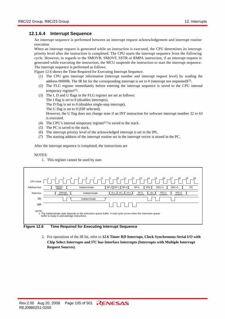
R8C/22 Group, R8C/23 Group 12. Interrupts
Rev.2.00 Aug 20, 2008 Page 105 of 501REJ09B0251-0200
12.1.6.4 Interrupt SequenceAn interrupt sequence is performed between an interrupt request acknowledgement and interrupt routineexecution. When an interrupt request is generated while an instruction is executed, the CPU determines its interruptpriority level after the instruction is completed. The CPU starts the interrupt sequence from the followingcycle. However, in regards to the SMOVB, SMOVF, SSTR or RMPA instruction, if an interrupt request isgenerated while executing the instruction, the MCU suspends the instruction to start the interrupt sequence.The interrupt sequence is performed as follows.Figure 12.6 shows the Time Required for Executing Interrupt Sequence.
(1) The CPU gets interrupt information (interrupt number and interrupt request level) by reading theaddress 00000h. The IR bit for the corresponding interrupt is set to 0 (interrupt not requested)(2).
(2) The FLG register immediately before entering the interrupt sequence is saved to the CPU internaltemporary register(1).
(3) The I, D and U flags in the FLG register are set as follows:The I flag is set to 0 (disables interrupts).The D flag is set to 0 (disables single-step interrupt).The U flag is set to 0 (ISP selected).However, the U flag does not change state if an INT instruction for software interrupt number 32 to 63is executed.
(4) The CPU’s internal temporary register(1) is saved to the stack.(5) The PC is saved to the stack.(6) The interrupt priority level of the acknowledged interrupt is set in the IPL.(7) The starting address of the interrupt routine set in the interrupt vector is stored in the PC.
After the interrupt sequence is completed, the instructions are
NOTES:1. This register cannot be used by user.
Figure 12.6 Time Required for Executing Interrupt Sequence
2. For operations of the IR bit, refer to 12.6 Timer RD Interrupt, Clock Synchronous Serial I/O with Chip Select Interrupts and I2C bus Interface Interrupts (Interrupts with Multiple Interrupt Request Sources).
1 2 3 4 5 6 7 8 9 10 11 12 13 14 15 16 17 18 19 20CPU clock
Address bus
Data bus
RD
WR
Address0000h Indeterminate
Indeterminate
Indeterminate
Interruptinformation
SP-2 SP-1 SP-4 SP-3 VEC VEC+1 VEC+2 PC
SP-2contents
SP-1contents
SP-4contents
SP-3 contents
VECcontents
VEC+1contents
VEC+2contents
NOTE:1. The indeterminate state depends on the instruction queue buffer. A read cycle occurs when the instruction queue
buffer is ready to acknowledge instructions.

R8C/22 Group, R8C/23 Group 12. Interrupts
Rev.2.00 Aug 20, 2008 Page 106 of 501REJ09B0251-0200
12.1.6.5 Interrupt Response TimeFigure 12.7 shows an Interrupt Response Time. The interrupt response time is the period between an interruptrequest generation and the execution of the first instruction in an interrupt routine. An interrupt response timeincludes the period between an interrupt request generation and the completed execution of an instruction(refer to (a) in Figure 12.7) and the period required to perform an interrupt sequence (20 cycles, refer to (b) inFigure 12.7).
Figure 12.7 Interrupt Response Time
12.1.6.6 IPL Change when Interrupt Request is AcknowledgedWhen an interrupt request of a maskable interrupt is acknowledged, the interrupt priority level of theacknowledged interrupt is set in the IPL.When a software interrupt and special interrupt request are acknowledged, the level listed in Table 12.5 is set tothe IPL.Table 12.5 lists the IPL Value When Software or Special Interrupt Is Acknowledged.
Table 12.5 IPL Value When Software or Special Interrupt Is AcknowledgedInterrupt Sources Value Set to IPL
Watchdog Timer, Oscillation Stop Detection, Voltage Monitor 2, Address Break 7Software, Address Match, Single-Step Not changed
Interrupt request is generated Interrupt request is acknowledged
Instruction Interrupt sequence Instruction ininterrupt routine
Time
(a) 20 Cycles (b)
Interrupt response time
(a) Period between an interrupt request generation and the completed execution of aninstruction. The length of this time varies depending on the instruction being executed.The DIVX instruction requires the longest time; 30 cycles (no wait and when the registeris set as the divisor)
(b) 21 cycles for address match and single-step interrupts.
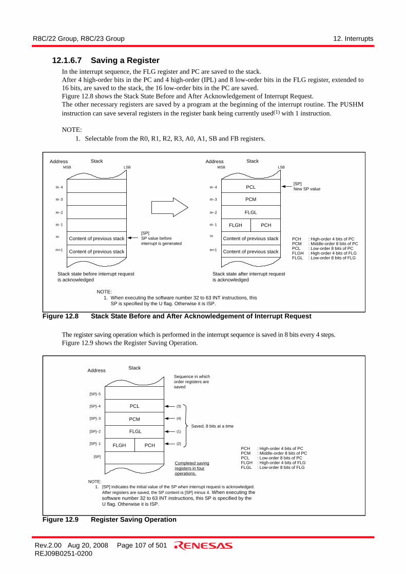
R8C/22 Group, R8C/23 Group 12. Interrupts
Rev.2.00 Aug 20, 2008 Page 107 of 501REJ09B0251-0200
12.1.6.7 Saving a RegisterIn the interrupt sequence, the FLG register and PC are saved to the stack.After 4 high-order bits in the PC and 4 high-order (IPL) and 8 low-order bits in the FLG register, extended to16 bits, are saved to the stack, the 16 low-order bits in the PC are saved.Figure 12.8 shows the Stack State Before and After Acknowledgement of Interrupt Request.The other necessary registers are saved by a program at the beginning of the interrupt routine. The PUSHMinstruction can save several registers in the register bank being currently used(1) with 1 instruction.
NOTE:1. Selectable from the R0, R1, R2, R3, A0, A1, SB and FB registers.
Figure 12.8 Stack State Before and After Acknowledgement of Interrupt Request
The register saving operation which is performed in the interrupt sequence is saved in 8 bits every 4 steps.Figure 12.9 shows the Register Saving Operation.
Figure 12.9 Register Saving Operation
Stack
[SP]SP value beforeinterrupt is generated
Content of previous stack
LSBMSBAddress
Content of previous stack
m−4
m−3
m−2
m−1
m
m+1
Stack state before interrupt requestis acknowledged
[SP]New SP value
Content of previous stack
LSBMSB
Content of previous stack
m
m+1
Stack state after interrupt requestis acknowledged
PCL
PCM
FLGL
FLGH PCH
m−4
m−3
m−2
m−1
StackAddress
PCH : High-order 4 bits of PCPCM : Middle-order 8 bits of PCPCL : Low-order 8 bits of PCFLGH : High-order 4 bits of FLGFLGL : Low-order 8 bits of FLG
NOTE:1. When executing the software number 32 to 63 INT instructions, this
SP is specified by the U flag. Otherwise it is ISP.
Stack
Completed savingregisters in fouroperations.
Address
[SP]−5
[SP]
PCL
PCM
FLGL
FLGH PCH
(3)
(4)
(1)
(2)
Saved, 8 bits at a time
Sequence in whichorder registers aresaved
NOTE:1. [SP] indicates the initial value of the SP when interrupt request is acknowledged.
After registers are saved, the SP content is [SP] minus 4. When executing the software number 32 to 63 INT instructions, this SP is specified by the
U flag. Otherwise it is ISP.
[SP]−4
[SP]−3
[SP]−2
[SP]−1PCH : High-order 4 bits of PCPCM : Middle-order 8 bits of PCPCL : Low-order 8 bits of PCFLGH : High-order 4 bits of FLGFLGL : Low-order 8 bits of FLG

R8C/22 Group, R8C/23 Group 12. Interrupts
Rev.2.00 Aug 20, 2008 Page 108 of 501REJ09B0251-0200
12.1.6.8 Returning from an Interrupt RoutineWhen the REIT instruction is executed at the end of an interrupt routine, the FLG register and PC, which havebeen saved to the stack, are automatically returned. The program, executed before the interrupt request hasbeen acknowledged, starts running again.Return the register saved by a program in an interrupt routine using the POPM instruction or others before theREIT instruction.
12.1.6.9 Interrupt PriorityIf two or more interrupt requests are generated while executing one instruction, the interrupt with the higherpriority is acknowledged. Set the ILVL2 to ILVL0 bits to select the desired priority level for maskable interrupts (peripheral functions).However, if two or more maskable interrupts have the same priority level, their interrupt priority is resolved byhardware, with the higher priority interrupt acknowledged in hardware.The priority levels of special interrupts such as reset (reset has the highest priority) and watchdog timer are setby hardware.Figure 12.10 shows the Priority Levels of Hardware Interrupts.The interrupt priority does not affect software interrupts. The MCU jumps to the interrupt routine when theinstruction is executed.
Figure 12.10 Priority Levels of Hardware Interrupts
Reset
Watchdog timerOscillation stop detection
Voltage monitor 2
Peripheral function
Single step
Address match
High
Low
Address break
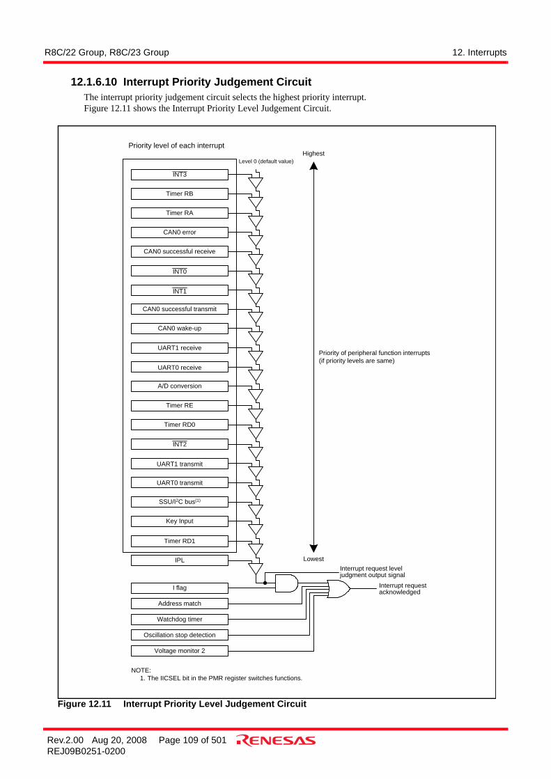
R8C/22 Group, R8C/23 Group 12. Interrupts
Rev.2.00 Aug 20, 2008 Page 109 of 501REJ09B0251-0200
12.1.6.10 Interrupt Priority Judgement CircuitThe interrupt priority judgement circuit selects the highest priority interrupt.Figure 12.11 shows the Interrupt Priority Level Judgement Circuit.
Figure 12.11 Interrupt Priority Level Judgement Circuit
INT3
Timer RB
Timer RA
INT0
CAN0 error
INT1
CAN0 successful receive
UART1 receive
UART0 receive
A/D conversion
SSU/I2C bus(1)
Key Input
IPL
Priority level of each interrupt
Level 0 (default value)
Lowest
Highest
Priority of peripheral function interrupts(if priority levels are same)
Interrupt request leveljudgment output signal
Interrupt requestacknowledgedI flag
Address match
Watchdog timer
Oscillation stop detection
Voltage monitor 2
NOTE: 1. The IICSEL bit in the PMR register switches functions.
UART0 transmit
CAN0 successful transmit
CAN0 wake-up
INT2
UART1 transmit
Timer RE
Timer RD0
Timer RD1

R8C/22 Group, R8C/23 Group 12. Interrupts
Rev.2.00 Aug 20, 2008 Page 110 of 501REJ09B0251-0200
12.2 INT Interrupt
12.2.1 INTi Interrupt (i = 0 to 3)The INTi interrupt is generated by an INTi input. When using the INTi interrupt, the INTiEN bit in the INTENregister is set to 1 (enable). The edge polarity is selected using the INTiPL bit in the INTEN register and thePOL bit in the INTiIC register.Inputs can be passed through a digital filter with three different sampling clocks. The INT0 pin is shared with the pulse output forced cutoff of timer RD and shared with the external triggerinput of timer RB.Figure 12.12 shows the INTEN Register. Figure 12.13 shows the INTF Register.
Figure 12.12 INTEN Register
External Input Enable Register
Symbol Address After ResetINTEN 00F9h 00h
Bit Symbol Bit Name Function RWINT0_____
input enable bit
INT0_____
input polarity select bit(1,2)
INT1_____
input enable bit
INT1_____
input polarity select bit(1,2)
INT2_____
input enable bit
INT2_____
input polarity select bit(1,2)
INT3_____
input enable bit
INT3_____
input polarity select bit(1,2)
NOTES:1.
2.
INT3PL
b3 b2 b1 b0b7 b6 b5 b4
RW
INT0EN
RW
INT1PL0 : One edge1 : Both edges RW
INT3EN
When setting the INTiPL bit (i = 0 to 3) to 1 (both edges), set the POL bit in the INTiIC register to 0 (selects fallingedge).The IR bit in the INTiIC register may be set to 1 (requests interrupt) w hen the INTiPL bit is rew ritten. Refer to 12.7.4Changing Interrupt Sources .
0 : Disable1 : Enable0 : One edge1 : Both edges
0 : One edge1 : Both edges
RW
INT0PL RW
INT1EN0 : Disable1 : Enable
0 : Disable1 : Enable RW
INT2EN0 : Disable1 : Enable RW
INT2PL0 : One edge1 : Both edges RW

R8C/22 Group, R8C/23 Group 12. Interrupts
Rev.2.00 Aug 20, 2008 Page 111 of 501REJ09B0251-0200
Figure 12.13 INTF Register
INT_____
Input Filter Select Register
Symbol Address After ResetINTF 00FAh 00h
Bit Symbol Bit Name Function RW
INT0_____
input f ilter select bits
INT1_____
input f ilter select bits
INT2_____
input f ilter select bits
INT3_____
input f ilter select bits
INT0F0 RW
INT0F1 RW
b7 b6 b5 b4 b3 b2 b1 b0
RW
b1 b0
0 0 : No f ilter0 1 : Filter w ith f1 sampling1 0 : Filter w ith f8 sampling1 1 : Filter w ith f32 sampling
RW
b7 b6
0 0 : No f ilter0 1 : Filter w ith f1 sampling1 0 : Filter w ith f8 sampling1 1 : Filter w ith f32 samplingINT3F1
INT3F0
INT1F0b3 b2
0 0 : No f ilter0 1 : Filter w ith f1 sampling1 0 : Filter w ith f8 sampling1 1 : Filter w ith f32 sampling
RW
INT1F1 RW
INT2F0b5 b4
0 0 : No f ilter0 1 : Filter w ith f1 sampling1 0 : Filter w ith f8 sampling1 1 : Filter w ith f32 sampling
RW
INT2F1 RW

R8C/22 Group, R8C/23 Group 12. Interrupts
Rev.2.00 Aug 20, 2008 Page 112 of 501REJ09B0251-0200
12.2.2 INTi Input Filter (i = 0 to 3)The INTi input contains a digital filter. The sampling clock is selected by the INTiF1 to INTiF0 bits in theINTF register. The IR bit in the INTiIC register is set to 1 (interrupt requested) when the INTi level is sampledfor every sampling clock and the sampled input level matches three times.Figure 12.14 shows the Configuration of INTi Input Filter. Figure 12.15 shows Operating Example of INTiInput Filter.
Figure 12.14 Configuration of INTi Input Filter
Figure 12.15 Operating Example of INTi Input Filter
i = 0 to 3INTiF0, INTiF1: Bits in INTF registerINTiEN, INTiPL: Bits in INTEN register
= 01b
INTi
Port directionregister(1)
Sampling clock
Digital filter(input level
matches 3x)
INTi interrupt
= 10b= 11bf32
f8f1
INTiF1 to INTiF0
INTiEN
Other thanINTiF1 to INTiF0= 00b
=00b INTiPL = 0
INTiPL = 1
NOTE:1. INT0: Port P4_5 direction register
INT1: Port P1_5 direction register when using P1_5 pinP1_7 direction register when using P1_7 pin
INT2: Port P6_6 direction registerINT3: Port P6_7 direction register
Both EdgesDetection
Circuit
INTi input
Samplingtiming
IR bit inINTiIC register
Set to 0 in program
NOTE:1. This is an operation example when the INTiF1 to INTiF0 bits in the
INTiF register is set to 01b, 10b, or 11b (passing digital filter).i = 0 to 3

R8C/22 Group, R8C/23 Group 12. Interrupts
Rev.2.00 Aug 20, 2008 Page 113 of 501REJ09B0251-0200
12.3 Key Input InterruptA key input interrupt request is generated by one of the input edges of the K10 to K13 pins. The key input interruptcan be used as a key-on wake-up function to exit wait or stop mode. The KIiEN (i = 0 to 3) bit in the KIEN register can select whether the pins are used as KIi input. The KIiPL bit inthe KIEN register can select the input polarity. When inputting “L” to the KIi pin which sets the KIiPL bit to 0 (falling edge), the input of the other K10 to K13pins are not detected as interrupts. Also, when inputting “H” to the KIi pin which sets the KIiPL bit to 1 (risingedge), the input of the other K10 to K13 pins are not detected as interrupts. Figure 12.16 shows a Block Diagram of Key Input Interrupt.
Figure 12.16 Block Diagram of Key Input Interrupt
KI3
Pull-uptransistor
KI2
Pull-uptransistor
KI3PL = 0
KI3PL = 1
PD1_3 bitKI3EN bit
PU02 bit in PUR0 register
PD1_3 bit in PD1 registerKUPIC register
Interrupt controlcircuit
Key input interruptrequest
KI2PL = 0
KI2PL = 1
PD1_2 bitKI2EN bit
KI1
Pull-uptransistor KI1PL = 0
KI1PL = 1
PD1_1 bitKI1EN bit
KI0
Pull-uptransistor KI0PL = 0
KI0PL = 1
PD1_0 bitKI0EN bit KI0EN, KI1EN, KI2EN, KI3EN,
KI0PL, KI1PL, KI2PL, KI3PL: Bits in KIEN registerPD1_0, PD1_1, PD1_2, PD1_3: Bits in PD1 register

R8C/22 Group, R8C/23 Group 12. Interrupts
Rev.2.00 Aug 20, 2008 Page 114 of 501REJ09B0251-0200
Figure 12.17 KIEN Register
Key Input Enable Register(1)
Symbol Address After ResetKIEN 00FBh 00h
Bit Symbol Bit Name Function RW
NOTE:1.
KI3 input polarity select bit 0 : Falling edge1 : Rising edge
KI0EN RW
KI0PL RW
KI0 input enable bit 0 : Disable1 : Enable
RW
0 : Disable1 : Enable
The IR bit in the KUPIC register may be set to 1 (requests interrupt) w hen the KIEN register is rew ritten.Refer to 12.7.4 Changing Interrupt Sources.
KI1EN RW
KI3ENKI3 input enable bit
KI3PL RW
KI2PLKI2 input polarity select bit 0 : Falling edge
1 : Rising edge
b1 b0b7 b6 b5 b4 b3 b2
RW
KI2EN RW
KI1PLKI1 input polarity select bit 0 : Falling edge
1 : Rising edgeKI2 input enable bit 0 : Disable
1 : Enable
RW
KI0 input polarity select bit 0 : Falling edge1 : Rising edge
KI1 input enable bit 0 : Disable1 : Enable

R8C/22 Group, R8C/23 Group 12. Interrupts
Rev.2.00 Aug 20, 2008 Page 115 of 501REJ09B0251-0200
12.4 CAN0 Wake-Up InterruptA CAN0 wake-up interrupt request is generated by a falling edge of the CRX pin. The CAN0 wake-up interrupt isenabled when the PortEn bit is 1 (CTX/CRX function) and Sleep bit is 1 (Sleep mode enabled) in the C0CTLRregister.Figure 12.18 shows the Block Diagram of CAN0 Wake-Up Interrupt.
Figure 12.18 Block Diagram of CAN0 Wake-Up Interrupt
CRXInterrupt control
circuit CAN0 wake-upinterrupt request
PortEn bit in C0CTLR register
Sleep bit in C0CTLR registerC01WKIC register

R8C/22 Group, R8C/23 Group 12. Interrupts
Rev.2.00 Aug 20, 2008 Page 116 of 501REJ09B0251-0200
12.5 Address Match InterruptAn address match interrupt request is generated immediately before executing the instruction at the addressindicated by the RMADi register (i = 0 or 1). This interrupt is used for a break function of the debugger. Whenusing the on-chip debugger, do not set an address match interrupt (the AIER, RMAD0 to RMAD1 registers, andrelocatable vector tables) in a user system.
Set the starting address of any instruction in the RMADi register. The AIER0 and AIER1 bits in the AIER0register can select to enable or disable the interrupt. The I flag and IPL do not affect the address match interrupt.The value of the PC (refer to 12.1.6.7 Saving a Register for the value of the PC) which is saved to the stack whenan address match interrupt is acknowledged varies depending on the instruction at the address indicated by theRMADi register (the appropriate return address is not pushed on the stack). When returning from the addressmatch interrupt, return by one of the following:
• Change the content of the stack and use the REIT instruction.• Use an instruction such as POP to restore the stack as it was before an interrupt request was acknowledged.
And then use a jump instruction.Table 12.6 lists the Value of PC Saved to Stack when Address Match Interrupt is Acknowledged. Figure 12.19shows the Registers AIER and RMAD0 to RMAD1.
NOTES:1. Refer to the 12.1.6.7 Saving a Register for the PC value saved.2. Operation code: Refer to the R8C/Tiny Series Software Manual (REJ09B0001).
Chapter 4. Instruction Code/Number of Cycles contains diagrams showing operation code below each syntax. Operation code is shown in the bold frame in the diagrams.
Table 12.6 Value of PC Saved to Stack when Address Match Interrupt is Acknowledged
Address Indicated by RMADi Register (i = 0 or 1) PC Value Saved(1)
• Instruction with 2-byte operation code(2)
• Instruction with 1-byte operation code(2)
ADD.B:S #IMM8,dest SUB.B:S #IMM8,dest AND.B:S #IMM8,destOR.B:S #IMM8,dest MOV.B:S #IMM8,dest STZ #IMM8,destSTNZ #IMM8,dest STZX #IMM81,#IMM82,destCMP.B:S #IMM8,dest PUSHM src POPM destJMPS #IMM8 JSRS #IMM8MOV.B:S #IMM,dest (However, dest = A0 or A1)
Address indicated by RMADi register + 2
Instructions other than the above Address indicated by RMADi register + 1
Table 12.7 Correspondence Between Address Match Interrupt Sources and Associated RegistersAddress Match Interrupt Source Address Match Interrupt Enable Bit Address Match Interrupt Register
Address Match Interrupt 0 AIER0 RMAD0Address Match Interrupt 1 AIER1 RMAD1

R8C/22 Group, R8C/23 Group 12. Interrupts
Rev.2.00 Aug 20, 2008 Page 117 of 501REJ09B0251-0200
Figure 12.19 Registers AIER and RMAD0 to RMAD1
Address Match Interrupt Enable Register
Symbol Address After ResetAIER 0013h 00h
Bit Symbol Bit Name Function RW
—(b7-b2) —
Nothing is assigned. If necessary, set to 0.When read, the content is 0.
b7 b6 b5 b4
0 : Disable1 : Enable RW
b3 b2 b1 b0
Address match interrupt 0 enable bit 0 : Disable1 : Enable RW
AIER1Address match interrupt 1 enable bit
AIER0
Address Match Interrupt Register i (i = 0 or 1)
b0
Symbol Address After ResetRMAD0 0012h-0010h 000000hRMAD1 0016h-0014h 000000h
Setting Range RW
(b16)b0
(b19)b3
(b23)b7
RW
——
(b7-b4)Nothing is assigned. If necessary, set to 0.When read, the content is 0.
Address setting register for address match interrupt
(b15)b7
(b8)b0 b7
00000h to FFFFFhFunction

R8C/22 Group, R8C/23 Group 12. Interrupts
Rev.2.00 Aug 20, 2008 Page 118 of 501REJ09B0251-0200
12.6 Timer RD Interrupt, Clock Synchronous Serial I/O with Chip Select Interruptsand I2C bus Interface Interrupts (Interrupts with Multiple Interrupt RequestSources)
Timer RD (channel 0), timer RD (channel 1), clock synchronous serial I/O with chip select and I2C bus interfacehave several interrupt request sources and an interrupt request is generated by the logical OR of several interruptrequest sources and the logical OR is reflected in the IR bit in the interrupt control register. Therefore, theseperipheral functions which have the status register of its own interrupt request sources (status register) and theenable register of the interrupt request sources (enable register) control the generations of the interrupt request(change of the IR bit in the interrupt control register). Table 12.8 lists the Registers Associated with Timer RDInterrupt, Clock Synchronous Serial I/O with Chip Select Interrupt, and I2C bus Interface Interrupt and Figure12.20 shows the Block Diagram of Timer RD Interrupt.
Figure 12.20 Block Diagram of Timer RD Interrupt
Table 12.8 Registers Associated with Timer RD Interrupt, Clock Synchronous Serial I/O with Chip Select Interrupt, and I2C bus Interface Interrupt
Status Register of Interrupt Request Source
Enable Register of Interrupt Request Source
Interrupt Control Register
Timer RD Channel 0 TRDSR0 TRDIER0 TRD0ICChannel 1 TRDSR1 TRDIER1 TRD1IC
Clock Synchronous Serial I/O with Chip Select
SSSR SSER SSUIC
I2C Bus Interface ICSR ICIER IICIC
Timer RD (channel i)Interrupt request(IR bit in TRDiIC register)
IMFA bitIMIEA bit
IMFB bitIMIEB bit
IMFC bitIMIEC bit
IMFD bitIMIED bit
UDF bitOVF bit
OVIE bit
i = 0 or 1IMFA, IMFB, IMFC, IMFD, OVF, UDF: Bits in TRDSRi registerIMIEA, IMIEB, IMIEC, IMIED, OVIE: Bits in TRDIER register
Channel i
R8C/22 Group, R8C/23 Group 12. Interrupts
Rev.2.00 Aug 20, 2008 Page 119 of 501REJ09B0251-0200
Controlling an interrupt with the I flag, IR bit, ILVL0 to ILVL2 bits and IPL by Timer RD (channel 0), Timer RD(channel 1), clock synchronous serial I/O with chip select and I2C bus interface is the same as that by othermaskable interrupts. However, since an interrupt source is generated based on multiple interrupt request sources,there are the following differences from other maskable interrupts:
• When bits in the enable register corresponding to set bits in the status register to 1 are set to 1 (enableinterrupt), the IR bit in the interrupt control register is set to 1 (interrupt requested).
• When either bits in the status register or bits in the enable register corresponding to bits in the status register, orboth of them are set to 0, the IR bit is set to 0 (interrupt not requested). Basically, even though the interrupt isnot acknowledged after the IR bit is set to 1, the interrupt request will not be maintained. Also, the IR bit is notset to 0 although 0 is written to the IR bit.
• Since each bit in the status register is not automatically set to 0 even if the interrupt is acknowledged.Therefore, the IR bit is not also automatically set to 0 when the interrupt is acknowledged. Set each bit in thestatus register to 0 in the interrupt routine. Refer to the status register figure how to set each bit in the statusregister to 0.
• When multiple bits in the enable register are set to 1 and other request sources are generated after the IR bit isset to 1, the IR bit remains 1.
• When multiple bits in the enable register are set to 1, determine by the status register which request sourcecauses an interrupt.
Refer to chapters of each peripheral function (14.3 Timer RD, 16.2 Clock Synchronous Serial I/O with ChipSelect (SSU) and 16.3 I2C Bus Interface) for the status register and enable register.Refer to 12.1.6 Interrupt Control for the interrupt control register.

R8C/22 Group, R8C/23 Group 12. Interrupts
Rev.2.00 Aug 20, 2008 Page 120 of 501REJ09B0251-0200
12.7 Notes on Interrupts
12.7.1 Reading Address 00000hDo not read the address 00000h by a program. When a maskable interrupt request is acknowledged, the CPUreads interrupt information (interrupt number and interrupt request level) from 00000h in the interruptsequence. At this time, the acknowledged interrupt IR bit is set to 0.If the address 00000h is read in a program, the IR bit for the interrupt which has the highest priority among theenabled interrupts is set to 0. This may cause a problem that the interrupt is canceled, or an unexpected interruptis generated.
12.7.2 SP SettingSet any value in the SP before an interrupt is acknowledged. The SP is set to 0000h after reset. Therefore, if aninterrupt is acknowledged before setting any value in the SP, the program may run out of control.
12.7.3 External Interrupt and Key Input InterruptEither an “L” level or an “H” level of width shown in the Electrical Characteristics is necessary for the signalinput to the INT0 to INT3 pins and KI0 to KI3 pins regardless of the CPU clocks. For details, refer to Table21.19 External Interrupt INTi (i = 0 to 3) Input, Table 21.25 External Interrupt INTi (i = 0 to 3) Input.

R8C/22 Group, R8C/23 Group 12. Interrupts
Rev.2.00 Aug 20, 2008 Page 121 of 501REJ09B0251-0200
12.7.4 Changing Interrupt SourcesThe IR bit in the interrupt control register may be set to 1 (interrupt requested) when the interrupt sourcechanges. When using an interrupt, set the IR bit to 0 (no interrupt requested) after changing the interrupt source.In addition, the changes of interrupt sources include all sources that change the interrupt sources assigned toindividual software interrupt numbers, polarities, and timing. Therefore, when a mode change of the peripheralfunctions involves interrupt sources, edge polarities, and timing, Set the IR bit to 0 (no interrupt requested) afterthe change. Refer to each peripheral function for the interrupts caused by the peripheral functions. Figure 12.21 shows an Example of Procedure for Changing Interrupt Sources.
Figure 12.21 Example of Procedure for Changing Interrupt Sources
NOTES:1. Execute the above settings individually. Do not execute two
or more settings at once (by one instruction).2. To prevent interrupt requests from being generated, disable
the peripheral function before changing the interruptsource. In this case, use the I flag if all maskable interruptscan be disabled. If all maskable interrupts cannot bedisabled, use bits ILVL0 to ILVL2 of the interrupt whosesource is changed.
3. Refer to 12.6.5 Changing Interrupt Control RegisterContents for the instructions to be used and usage notes.
Interrupt source change
Disable interrupts(2, 3)
Set the IR bit to 0 (interrupt not requested)using the MOV instruction(3)
Change interrupt source (including modeof peripheral function)
Enable interrupts(2, 3)
Change completed
IR bit: The interrupt control register bit of aninterrupt whose source is changed.

R8C/22 Group, R8C/23 Group 12. Interrupts
Rev.2.00 Aug 20, 2008 Page 122 of 501REJ09B0251-0200
12.7.5 Changing Interrupt Control Register Contents(a) Each interrupt control register can only be changed while interrupt requests corresponding to that
register are not generated. If interrupt requests may be generated, disable the interrupts before changingthe interrupt control register.
(b) When changing any interrupt control register after disabling interrupts, be careful with the instructionsto be used.When changing any bit other than IR bitIf an interrupt request corresponding to that register is generated while executing the instruction, the IRbit may not be set to 1 (interrupt requested), and the interrupt request may be ignored. If this causes aproblem, use the following instructions to change the register.Instructions to use: AND, OR, BCLR, BSETWhen changing IR bitIf the IR bit is set to 0 (interrupt not requested), it may not be set to 0 depending on the instruction to beused. Therefore, use the MOV instruction to set the IR bit to 0.
(c) When disabling interrupts using the I flag, set the I flag according to the following sample programs.Refer to (b) for the change of interrupt control registers in the sample programs.
Sample programs 1 to 3 are preventing the I flag from being set to 1 (interrupt enables) before changing theinterrupt control register for reasons of the internal bus or the instruction queue buffer.
Example 1: Use NOP instructions to prevent I flag being set to 1 before interrupt control register ischanged
INT_SWITCH1:FCLR I ; Disable interruptsAND.B #00H,0056H ; Set TRAIC register to 00hNOP ;NOPFSET I ; Enable interrupts
Example 2: Use dummy read to have FSET instruction waitINT_SWITCH2:
FCLR I ; Disable interruptsAND.B #00H,0056H ; Set TRAIC register to 00hMOV.W MEM,R0 ; Dummy readFSET I ; Enable interrupts
Example 3: Use POPC instruction to change I flagINT_SWITCH3:
PUSHC FLGFCLR I ; Disable interruptsAND.B #00H,0056H ; Set TRAIC register to 00hPOPC FLG ; Enable interrupts

R8C/22 Group, R8C/23 Group 13. Watchdog Timer
Rev.2.00 Aug 20, 2008 Page 123 of 501REJ09B0251-0200
13. Watchdog TimerThe watchdog timer is a function to detect when the program is out of control. To use the watchdog timer isrecommend for improving reliability of a system. The watchdog timer contains a 15-bit counter and can select countsource protection mode is enabled or disabled.Table 13.1 lists the Count Source Protection Mode Refer to 5.5 Watchdog Timer Reset for details of the watchdog timer reset.Figure 13.1 shows the Block Diagram of Watchdog Timer, Figure 13.2 shows Registers OFS and WDC and Figure13.3 shows Registers WDTR, WDTS, and CSPR.
Figure 13.1 Block Diagram of Watchdog Timer
Table 13.1 Count Source Protection Mode
Item Count Source ProtectionMode Disabled
Count Source ProtectionMode Enabled
Count Source CPU clock Low-speed on-chip oscillator clock
Count Operation DecrementCount Start Condition Either of following can be selected
• After reset, count starts automatically• Count starts by writing to WDTS register
Count Stop Condition Stop mode, wait mode NoneReset Condition of Watchdog Timer
• Reset• Write 00h to the WDTR register before writing FFh• Underflow
Operation at the Time of Underflow
Watchdog timer interrupt or watchdog timer reset
Watchdog timer reset
CPU clock
1/16
1/128 Watchdog timer
Internal reset signal(“L” active)
Write to WDTR register
WDC7 = 0
WDC7 = 1
Set to7FFFh(1)
PM12 = 1 Watchdog timer reset
PM12 = 0 Watchdog timer interrupt request
Prescaler
CSPRO = 0
fOCO-SCSPRO = 1
CSPRO: Bit in CSPR registerWDC7: Bit in WDC registerPM12: Bit in PM1 register
NOTE: 1. When the CSPRO bit is set to 1 (count source protection mode enabled), 0FFFh is set.

R8C/22 Group, R8C/23 Group 13. Watchdog Timer
Rev.2.00 Aug 20, 2008 Page 124 of 501REJ09B0251-0200
Figure 13.2 Registers OFS and WDC
Watchdog Timer Control Register
Symbol Address After ResetWDC 000Fh 00X11111b
Bit Symbol Bit Name Function RW
—(b5)
Reserved bits Set to 0.When read, the content is undefined. RW
RW
High-order bits of w atchdog timer
b3 b2 b1 b0
—(b4-b0) RO
b7 b6 b5 b4
0 0
RW
WDC7
—(b6)
Reserved bits Set to 0
Prescaler select bit 0 : Divide-by-161 : Divide-by-128
Option Function Select Register(1)
Symbol Address Before ShipmentOFS 0FFFFh FFh(3)
Bit Symbol Bit Name Function RW
Reserved bit
NOTES:1.
2.3.
b7 b6 b5 b4 b3 b2 b1 b0
1 1 1
—(b1)
Set to 1RW
WDTONWatchdog timer startselect bit
0 : Starts w atchdog timer automatically after reset1 : Watchdog timer is inactive after reset RW
ROMCRROM code protectdisabled bit
0 : ROM code protect disabled1 : ROMCP1 enabled RW
ROMCP1ROM code protect bit 0 : ROM code protect enabled
1 : ROM code protect disabled RW
RW
—(b5-b4)
Reserved bits Set to 1RW
If the block including the OFS register is erased, FFh is set to the OFS register.To use the pow er-on reset, set the LVD1ON bit to 0 (voltage monitor 1 reset enabled after reset).
LVD1ONVoltage detection circuitstart bit(2)
0 : Voltage monitor 1 reset enabled after reset1 : Voltage monitor 1 reset disabled after reset RW
The OFS register is on the f lash memory. Write to the OFS register w ith a program. After w riting is completed, do notw rite additions to the OFS register.
CSPROINICount source protectmode after reset selectbit
0 : Count source protect mode enabled after reset1 : Count source protect mode disabled after reset

R8C/22 Group, R8C/23 Group 13. Watchdog Timer
Rev.2.00 Aug 20, 2008 Page 125 of 501REJ09B0251-0200
Figure 13.3 Registers WDTR, WDTS, and CSPR
Watchdog Timer Reset Register
Symbol Address After ResetWDTR 000Dh Indeterminate
RW
NOTES:1.2.
FunctionWhen w riting 00h before w riting FFh, the w atchdog timer is reset.(1)
The default value of the w atchdog timer is set to 7FFFh w hen count source protectionmode is disabled and 0FFFh w hen count source protection mode is enabled.(2)
b7 b0
Do not generate an interrupt betw een 00h and the FFh w ritings.When the CSPRO bit in the CSPR register is set to 1 (count source protection mode enabled),0FFFh is set to the w atchdog timer.
WO
Watchdog Timer Start Register
Symbol Address After ResetWDTS 000Eh Indeterminate
RW
WO
FunctionThe w atchdog timer starts counting after a w rite instruction to this register.
b0b7
Count Source Protection Mode Register
Symbol Address After Reset(1)
CSPR 001Ch 00hBit Symbol Bit Name Function RW
NOTES:1.2.
—(b6-b0) RW
00
Write 0 before w riting 1 to set the CSPRO bit to 1.0 cannot be set by a program.
When w riting 0 to the CSPROINI bit in the OFS register, the value after reset is set to 10000000b.
0
Reserved bits Set to 0
b3 b2 b1 b0b7 b6 b5 b4
RW
0 0 0 0
CSPROCount source protection modeselect bit(2)
0 : Count source protection mode disabled1 : Count source protection mode enabled

R8C/22 Group, R8C/23 Group 13. Watchdog Timer
Rev.2.00 Aug 20, 2008 Page 126 of 501REJ09B0251-0200
13.1 Count Source Protection Mode DisabledThe count source of the watchdog timer is the CPU clock when count source protection mode is disabled.Table 13.2 lists the Watchdog Timer Specifications (with Count Source Protection Mode Disabled).
NOTES:1. The watchdog timer is reset when writing 00h to the WDTR register before writing FFh. The
prescaler is reset after the MCU is reset. Some errors occur by the prescaler for the period of the watchdog timer.
2. The WDTON bit cannot be changed by a program. When setting the WDTON bit, write 0 to the bit 0 of the address 0FFFFh using a flash programmer.
Table 13.2 Watchdog Timer Specifications (with Count Source Protection Mode Disabled)Item Specification
Count Source CPU clockCount Operation DecrementPeriod Division ratio of prescaler(n) x count value of watchdog timer(32768)(1)
CPU clockn: 16 or 128 (selected by WDC7 bit in WDC register)e.g.When the CPU clock is 16 MHz and prescaler is divided by 16, the
period is approximately 32.8 msCount Start Condition The WDTON bit(2) in the OFS register (0FFFFh) selects the operation
of watchdog timer after reset• When the WDTON bit is set to 1 (watchdog timer is in stop state after
reset)The watchdog timer and prescaler stop after reset and the count starts by writing to the WDTS register
• When the WDTON bit is set to 0 (watchdog timer starts automatically after exiting)The watchdog timer and prescaler start counting automatically after reset
Reset Condition of Watchdog Timer
• Reset• Write 00h to the WDTR register before writing FFh• Underflow
Count Stop Condition Stop and wait modes (inherit the count from the held value after exiting modes)
Operation at the Time of Underflow
• When the PM12 bit in the PM1 register is set to 0Watchdog timer interrupt
• When the PM12 bit in the PM1 register is set to 1Watchdog timer reset (refer to 5.5 Watchdog Timer Reset)

R8C/22 Group, R8C/23 Group 13. Watchdog Timer
Rev.2.00 Aug 20, 2008 Page 127 of 501REJ09B0251-0200
13.2 Count Source Protection Mode EnabledThe count source of the watchdog timer is the low-speed on-chip oscillator clock when count source protectionmode is enabled. If the CPU clock stops when the program is out of control, the clock can be supplied to thewatchdog timer.Table 13.3 lists the Watchdog Timer Specifications (with Count Source Protection Mode Enabled).
NOTES:1. The WDTON bit cannot be changed by a program. When setting the WDTON bit, write 0 to the bit 0
of the address 0FFFFh using a flash programmer.2. Even if writing 0 to the CSPROINI bit in the OFS register, the CSPRO bit is set to 1. The CSPROINI
bit cannot be changed by a program. When setting the CSPROINI bit, write 0 to the bit 7 of the address 0FFFFh using a flash programmer.
Table 13.3 Watchdog Timer Specifications (with Count Source Protection Mode Enabled)Item Specification
Count Source Low-speed on-chip oscillator clockCount Operation DecrementPeriod Count value of watchdog timer (4096)
Low-speed on-chip oscillator clocke.g. Period is approximately 32.8 ms when the low-speed on-chip
oscillator clock is 125 kHzCount Start Condition The WDTON bit(1) in the OFS register (0FFFFh) selects the operation
of the watchdog timer after reset.• When the WDTON bit is set to 1 (watchdog timer is in stop state
after reset)The watchdog timer and prescaler stop after reset and the count starts by writing to the WDTS register
• When the WDTON bit is set to 0 (watchdog timer starts automatically after reset)The watchdog timer and prescaler start counting automatically after reset
Reset Condition of Watchdog Timer
• Reset• Write 00h to the WDTR register before writing FFh• Underflow
Count Stop Condition None (the count does not stop in wait mode after the count starts. The MCU does not enter stop mode)
Operation at the Time of Underflow
Watchdog timer reset (refer to 5.5 Watchdog Timer Reset)
Register, Bit • When setting the CSPPRO bit in the CSPR register to 1 (count source protection mode is enabled)(2), the following are set automatically- Set 0FFFh to the watchdog timer- Set the CM14 bit in the CM1 register to 0 (low-speed on-chip
oscillator on)- Set the PM12 bit in the PM1 register to 1 (The watchdog timer is
reset when watchdog timer underflows)• The following states are held in count source protection mode
- Writing to the CM10 bit in the CM1 register disables (It remains unchanged even if it is set to 1. The MCU does not enter stop mode)- Writing to the CM14 bit in the CM1 register disables (It remains unchanged even if it is set to 1. The low-speed on-chip oscillator does not stop)

R8C/22 Group, R8C/23 Group 14. Timers
Rev.2.00 Aug 20, 2008 Page 128 of 501REJ09B0251-0200
14. TimersThe MCU contains two 8-bit timers with 8-bit prescaler, two 16-bit timers, and a timer with a 4-bit counter, and an 8-bit counter. The two 8-bit timers with the 8-bit prescaler contain timer RA and timer RB. These timers contain a reloadregister to memorize the default value of the counter. The 16-bit timer is timer RD which contains the input capture andoutput compare. The 4 and 8-bit counters are timer RE which contains the output compare. All these timers operateindependently. Table 14.1 lists Functional Comparison of Timers.

R8C/22 Group, R8C/23 Group 14. Timers
Rev.2.00 Aug 20, 2008 Page 129 of 501REJ09B0251-0200
NOTE:1. The underflow interrupt can be set to channel 1.
Table 14.1 Functional Comparison of TimersItem Timer RA Timer RB Timer RD Timer RE
Configuration 8-bit timer with 8-bit prescaler (with reload register)
8-bit timer with 8-bit prescaler (with reload register)
16-bit free-run timer X 2 (with input capture and output compare)
4-bit counter8-bit counter
Count Decrement Decrement Increment / Decrement IncrementCount Sources • f1
• f2• f8• fOCO
• f1• f2• f8• Timer RA
underflow
• f1• f2• f4• f8• f32• fOCO40M• TRDIOA0
• f4• f8• f32
Function Timer mode provided provided provided(input capture function, output compare function)
not provided
Pulse output mode provided not provided not provided not providedEvent counter mode provided not provided not provided not providedPulse width measurement mode
provided not provided not provided not provided
Pulse period measurement mode
provided not provided not provided not provided
Programmable waveform generation mode
not provided provided not provided not provided
Programmable one-shot generation mode
not provided provided not provided not provided
Programmable wait one-shot generation mode
not provided provided not provided not provided
Input capture mode not provided not provided provided not providedOutput compare mode
not provided not provided provided provided
PWM mode not provided not provided provided not providedReset synchronized PWM mode
not provided not provided provided not provided
Complementary PWM mode
not provided not provided provided not provided
PWM3 mode not provided not provided provided not providedInput Pin TRAIO INT0 INT0, TRDCLK
TRDIOA0, TRDIOA1,TRDIOB0, TRDIOB1,TRDIOC0, TRDIOC1,TRDIOD0, TRDIOD1
-
Output Pin TRAOTRAIO
TRBO TRDIOA0, TRDIOA1,TRDIOB0, TRDIOB1,TRDIOC0, TRDIOC1,TRDIOD0, TRDIOD1
TREO
Related Interrupt Timer RA intINT1 int
Timer RB intINT0 int
Compare match / input capture A0 to D0 intCompare match / input capture A1 to D1 intOverflow intUnderflow int(1)
INT0 int
Timer RE int
Timer Stop provided provided provided provided

R8C/22 Group, R8C/23 Group 14. Timers
Rev.2.00 Aug 20, 2008 Page 130 of 501REJ09B0251-0200
14.1 Timer RATimer RA is an 8-bit timer with an 8-bit prescaler.The prescaler and timer consist of the reload register and counter. The reload register and counter are allocated atthe same address. When accessing the TRAPRE and TRA registers, the reload register and counter can be accessed(refer to Table 14.2 to 14.6 the Specification of Each Modes).The count source for timer RA is the operating clock that regulates the timing of timer operations such as countingand reloading.Figure 14.1 shows the Block Diagram of Timer RA. Figures 14.2 to 14.4 show the registers associated with TimerRA.
Timer RA contains five operation modes listed as follows:• Timer mode: The timer counts an internal count source.• Pulse output mode: The timer counts an internal count source and outputs the pulses which
invert the polarity by underflow of the timer.• Event counter mode: The timer counts external pulses.• Pulse width measurement mode: The timer measures the pulse width of an external pulse.• Pulse period measurement mode: The timer measures the pulse period of an external pulse.
Figure 14.1 Block Diagram of Timer RA
TMOD2 to TMOD0= 010b
= 000b= 001b
= 011bf2
f8f1
= 010bfOCO
TCK2 to TCK0 bit
Counter
Reloadregister
TRAPRE register(Prescaler)
Peripheral data bus
Timer RA interrupt
Write to TRAMR registerWrite to TSTOP bit 1
TCSTF, TSTOP: TRACR registerTEDGSEL, TOPCR, TOENA, TIOSEL, TIPF1, TIPF0: TRAIOC registerTMOD2 to TMOD0, TCK2 to TCK0, TCKCUT: TRAMR register
Toggle flip-flopQ
Q CLR
CK
TOENA bit
TRAO pin
INT1/TRAIO (P1-5) pin
TCSTFbit
TMOD2 to TMOD0= 011b or 100b
Polarityswitching
Digitalfilter
Counter
Reloadregister
TRA register(Timer)
TIPF1 to TIPF0 bit= 00b= 10bf8
f1
= 11bf32
TIOSEL = 0
TIOSEL = 1
Count controlcircle
TMOD2 to TMOD0 = 001bTOPCR bit
Underflow signal
Measurement completion signal
TIPF1 toTIPF0 bit= Except 00b
= 00b
INT1/TRAIO (P1-7) pin
TEDGSEL = 1
TEDGSEL = 0
TMOD2 to TMOD0= Except 010b
TCKCUTbit

R8C/22 Group, R8C/23 Group 14. Timers
Rev.2.00 Aug 20, 2008 Page 131 of 501REJ09B0251-0200
Figure 14.2 Registers TRACR and TRAIOC
Timer RA Control Register(4)
Symbol Address After ResetTRACR 0100h 00h
Bit Symbol Bit Name Function RW
NOTES:1.2.
3.
4.
5.
In pulse w idth measurement mode and pulse period measurement mode, use the MOV instruction to set the TRACRregister. If it is necessary to avoid changing the values of bits TEDGF and TUNDF, w rite 1 to them.Set to 0 in timer mode, pulse output mode, and event counter mode.
Bits TEDGF and TUNDF can be set to 0 by w riting 0 to these bits by a program. How ever, their value remainsunchanged w hen 1 is w ritten.
0 : Stops counting1 : Starts counting
Timer RA count status f lag(1)
TSTOP RW
—
TEDGF0 : Active edge not received1 : Active edge received (end of measurement period)
RW
TUNDF
Timer RA count start bit(1)
Timer RA count forcible stopbit(2)
Active edge receptionflag(3,5)
TSTART
b7 b6 b5 b4
RWTimer RA underflow f lag(3,5) 0 : No underflow
1 : Underflow
b3 b2
When this bit is set to 1, the count is forciblystopped. When read, the content is 0.
—(b3)
b1 b0
RW
TCSTF
When the TSTOP bit is set to 1, bits TSTART and TCSTF and registers TRAPRE and TRA are set to the values after areset.
0 : Stops counting1 : Counting
Nothing is assigned. If necessary, set to 0.When read, the content is 0.
Nothing is assigned. If necessary, set to 0.When read, the content is 0.
RO
—(b7-b6) —
Refer to 14.1.6 Notes on Timer RA.
Timer RA I/O Control Register
Symbol Address After ResetTRAIOC 0101h 00h
Bit Symbol Bit Name Function RW
RWTIPF0
TOENA RW
TRAIO input f ilter select bitsTIPF1
RWRW
Function varies depending on operation mode
—
TEDGSEL RWTOPCR RW
TRAIO polarity sw itch bit
Nothing is assigned. If necessary, set to 0.When read, the content is 0.
—(b7-b6)
TRAIO output control bit
INT1_____
/TRAIO select bitTRAO output enable bit
b7 b6 b5 b4 b3 b2
TIOSEL
b1 b0

R8C/22 Group, R8C/23 Group 14. Timers
Rev.2.00 Aug 20, 2008 Page 132 of 501REJ09B0251-0200
Figure 14.3 Registers TRAMR and TRAPRE
Timer RA Mode Register(1)
Symbol Address After ResetTRAMR 0102h 00h
Bit Symbol Bit Name Function RW
NOTE:1.
RW
—
TCK0 RW
When both the TSTART and TCSTF bits in the TRACR register are set to 0 (count stops), rew rite this register.
RW
Timer RA count sourcecutoff bit
0 : Provides count source1 : Cuts off count source
TCK2
RW
TMOD1 RW
TMOD0Timer RA operation modeselect bits
b2 b1 b0
0 0 0 : Timer mode0 0 1 : Pulse output mode0 1 0 : Event counter mode0 1 1 : Pulse w idth measurement mode1 0 0 : Pulse period measurement mode1 0 1 :1 1 0 : Do not set1 1 1 :
b7 b6 b5 b4
RW
Timer RA count sourceselect bits
b6 b5 b4
0 0 0 : f10 0 1 : f80 1 0 : fOCO0 1 1 : f21 0 0 :1 0 1 : Do not set1 1 0 :1 1 1 :
Nothing is assigned. If necessary, set to 0.When read, the content is 0.
TMOD2
RW
TCKCUT
TCK1
b3 b2
—(b3)
b1 b0
Timer RA Prescaler Register
Symbol Address After ResetTRAPRE 0103h FFh(1)
Mode Function Setting Range RW
NOTE:1. When the TSTOP bit in the TRACR register is set to 1, the TRA register is set to FFh.
Event Counter Mode Counts an external count source 00h to FFh RWCounts an internal count source
00h to FFh RW
Pulse PeriodMeasurement Mode
Counts an internal count source
Pulse Output Mode RWCounts an internal count source 00h to FFhRWCounts an internal count source 00h to FFh
b7
00h to FFh RW
Pulse WidthMeasurement Mode
b0
Timer Mode

R8C/22 Group, R8C/23 Group 14. Timers
Rev.2.00 Aug 20, 2008 Page 133 of 501REJ09B0251-0200
Figure 14.4 TRA Register
Timer RA Register
Symbol Address After ResetTRA 0104h FFh(1)
Mode Function Setting Range RW
NOTE:1.
00h to FFh
b7
When the TSTOP bit in the TRACR register is set to 1, the TRA register is set to FFh.
b0
All ModesCounts of an underflow of the TRAPREregister RW

R8C/22 Group, R8C/23 Group 14. Timers
Rev.2.00 Aug 20, 2008 Page 134 of 501REJ09B0251-0200
14.1.1 Timer ModeIn this mode, the timer counts an internally generated count source (see Table 14.2 Timer ModeSpecifications).Figure 14.5 shows the TRAIOC Register in Timer Mode.
Figure 14.5 TRAIOC Register in Timer Mode
Table 14.2 Timer Mode SpecificationsItem Specification
Count Sources f1, f2, f8, fOCOCount Operations • Decrement
• When the timer underflows, the contents in the reload register is reloaded and the count is inherited
Divide Ratio 1/(n+1)(m+1)n: setting value of TRAPRE register, m: setting value of TRA register
Count Start Condition Write 1 (count starts) to the TSTART bit in the TRACR registerCount Stop Conditions • Write 0 (count stops) to the TSTART bit in the TRACR register
• Write 1 (count forcibly stops) to the TSTOP bit in the TRACR registerInterrupt Request Generation Timing
When Timer RA underflows [Timer RA interrupt]
INT1/TRAIO Pin Function
Programmable I/O port or INT1 interrupt input
TRAO Pin Function Programmable I/O portRead from Timer The count value can be read by reading the TRA and TRAPRE registersWrite to Timer • When registers TRAPRE and TRA are written while the count is stopped,
values are written to both the reload register and counter.• When registers TRAPRE and TRA are written during the count, values are
written to the reload register and counter (refer to 14.1.1.1 Timer Write Control during Count Operation).
Timer RA I/O Control Register
Symbol Address After ResetTRAIOC 0101h 00h
Bit Symbol Bit Name Function RW
INT1/_____
TRAIO select bit 0 : INT1_____
/TRAIO pin (P1_7)1 : INT1
_____/TRAIO pin (P1_5)
b3 b2
TIOSEL
b1 b0
00b7 b6 b5 b4
Nothing is assigned. If necessary, set to 0.When read, the content is 0.
0 0 0
—(b7-b6)
TEDGSEL
TRAO output enable bit
TRAIO input filter select bits
—
TOPCR RWTOENA RW
RW
TIPF0TIPF1
RWRW
Set to 0 in timer mode
RWTRAIO polarity sw itch bitTRAIO output control bit
Set to 0 in timer mode

R8C/22 Group, R8C/23 Group 14. Timers
Rev.2.00 Aug 20, 2008 Page 135 of 501REJ09B0251-0200
14.1.1.1 Timer Write Control during Count OperationTimer RA has a prescaler and a timer (which counts the prescaler underflows). The prescaler and timer eachconsist of a reload register and a counter. When writing to the prescaler or timer, values are written to both thereload register and counter.However, values are transferred from the reload register to the counter of the prescaler in synchronization withthe count source. In addition, values are transferred from the reload register to the counter of the timer insynchronization with prescaler underflows. Therefore, if the prescaler or timer is written to when countoperation is in progress, the counter value is not updated immediately after the WRITE instruction is executed.Figure 14.6 shows an Operating Example of Timer RA when Counter Value is Rewritten during CountOperation.
Figure 14.6 Operating Example of Timer RA when Counter Value is Rewritten during Count Operation
Count source
Reloads register oftimer RA prescaler
IR bit in TRAICregister 0
Counter oftimer RA prescaler
Reloads register oftimer RA
Counter of timer RA
Set 01h to the TRAPRE register and 25h tothe TRA register by a program.
After writing, the reload register iswritten to at the first count source.
Reload atsecond countsource
Reload atunderflow
After writing, the reload register iswritten to at the first underflow.
Reload at the second underflow
The IR bit remains unchanged until underflow isgenerated by a new value.
05h 04h 01h 00h 01h 00h 01h 00h 01h 00h06h
New value (01h)Previous value
New value (25h)Previous value
03h 24h02h 25h
The above applies under the following conditions.Both bits TSTART and TCSTF in the TRACR register are set to 1 (During count).

R8C/22 Group, R8C/23 Group 14. Timers
Rev.2.00 Aug 20, 2008 Page 136 of 501REJ09B0251-0200
14.1.2 Pulse Output ModePulse output mode is mode to count the count source internally generated and outputs the pulse which invertsthe polarity from the TRAIO pin each time the timer underflows (see Table 14.3 Pulse Output ModeSpecifications).Figure 14.7 shows the TRAIOC Register in Pulse Output Mode.
NOTE:1. The level of output pulse turn into the level when the pulse output starts by writing the TRAMR
register.
Table 14.3 Pulse Output Mode SpecificationsItem Specification
Count Sources f1, f2, f8, fOCOCount Operations • Decrement
• When the timer underflows, the contents in the reload register is reloaded and the count is inherited
Divide Ratio 1/(n+1)(m+1)n: setting value of TRAPRE register, m: setting value of TRA register
Count Start Condition Write 1 (count starts) to the TSTART bit in the TRACR registerCount Stop Conditions • Write 0 (count stops) to the TSTART bit in the TRACR register
• Write 1 (count forcibly stops) to the TSTOP bit in the TRACR registerInterrupt Request Generation Timing
When timer RA underflows [timer RA interrupt]
INT1/TRAIO Pin Function
Pulse output, programmable output port, or INT1 interrupt(1)
TRAO Pin Function Programmable I/O port or inverted output of TRAIO(1)
Read from Timer The count value can be read by reading the TRA and TRAPRE registersWrite to Timer • When registers TRAPRE and TRA are written while the count is stopped,
values are written to both the reload register and counter.• When registers TRAPRE and TRA are written during the count, values are
written to the reload register and counter (refer to 14.1.1.1 Timer Write Control during Count Operation).
Select Functions • TRAIO output polarity switch functionThe TEDGSEL bit in the TRAIOC register can select the polarity level when the pulse output starts(1)
• Inverted pulse output functionThe pulse which inverts the polarity of the TRAIO output can be output from the TRAO pin (selected by the TOENA bit in the TRAIOC register)
• Pulse output stop functionThe pulse output from the TRAIO pin can be stopped by the TOPCR bit.
• INT1/TRAIO pin select functionP1_7 or P1_5 is selected by the TIOSEL bit in the TRAIOC register.

R8C/22 Group, R8C/23 Group 14. Timers
Rev.2.00 Aug 20, 2008 Page 137 of 501REJ09B0251-0200
Figure 14.7 TRAIOC Register in Pulse Output Mode
Timer RA I/O Control Register
Symbol Address After ResetTRAIOC 0101h 00h
Bit Symbol Bit Name Function RW
INT1_____
/TRAIO select bit 0 : INT1_____
/TRAIO pin (P1_7)1 : INT1
_____/TRAIO pin (P1_5)
RWRW
0 : TRAIO output1 : Port P1_7 or P1_5
Nothing is assigned. If necessary, set to 0.When read, the content is 0.
TRAO output enable bit
TRAIO input filter select bits Set to 0 in pulse output mode
TEDGSEL RWTRAIO polarity sw itch bit
TIPF1—
(b7-b6) —
TOPCR RW
TOENA RW
RW
TIPF0
TRAIO output control bit
0 0b7 b6 b5 b4 b3 b2
0 : Port P3_01 : TRAO output (Inverted TRAIO output from P3_0)
TIOSEL
b1 b0
0 : TRAIO output starts at “H”1 : TRAIO output starts at “L”

R8C/22 Group, R8C/23 Group 14. Timers
Rev.2.00 Aug 20, 2008 Page 138 of 501REJ09B0251-0200
14.1.3 Event Counter ModeEvent counter mode is mode to count an external signal which inputs from the INT1/TRAIO pin (see Table14.4 Event Counter Mode Specifications).Figure 14.8 shows the TRAIOC Register in Event Counter Mode.
NOTE:1. The level of output pulse turn into the level when the pulse output starts by writing the TRAMR
register.
Table 14.4 Event Counter Mode SpecificationsItem Specification
Count Source External signal which is input to TRAIO pin (active edge is selectable by a program)
Count Operations • Decrement• When the timer underflows, the contents in the reload register is reloaded and
the count is inheritedDivide Ratio 1/(n+1)(m+1)
n: setting value of TRAPRE register, m: setting value of TRA registerCount Start Condition Write 1 (count starts) to the TSTART bit in the TRACR registerCount Stop Conditions
• Write 0 (count stops) to the TSTART bit in the TRACR register• Write 1 (count forcibly stops) to the TSTOP bit in the TRACR register
Interrupt Request Generation Timing
When timer RA underflows [timer RA interrupt]
INT1/TRAIO Pin Function
Count source input (INT1 interrupt input)
TRAO Pin Function Programmable I/O port(1)
Read from Timer The count value can be read by reading the TRA and TRAPRE registersWrite to Timer • When registers TRAPRE and TRA are written while the count is stopped, values
are written to both the reload register and counter.• When registers TRAPRE and TRA are written during the count, values are
written to the reload register and counter (refer to 14.1.1.1 Timer Write Control during Count Operation).
Select Functions • INT1 input polarity switch functionThe TEDGSEL bit in the TRAIOC register can select the active edge of the count source.
• Count source input pin select functionP1_7 or P1_5 is selected by the TIOSEL bit in the TRAIOC register.
• Pulse output functionThe pulse which inverts the polarity can be output from the TRAO pin each time the timer underflows. (selected by the TOENA bit in the TRAIOC register)(1)
• Digital filter functionBits TIPF0 and TIPF1 in the TRAIOC register enable or disable the digital filter and select the sampling frequency.

R8C/22 Group, R8C/23 Group 14. Timers
Rev.2.00 Aug 20, 2008 Page 139 of 501REJ09B0251-0200
Figure 14.8 TRAIOC Register in Event Counter Mode
Timer RA I/O Control Register
Symbol Address After ResetTRAIOC 0101h 00h
Bit Symbol Bit Name Function RW
INT1_____
/TRAIO select bit 0 : INT1_____
/TRAIO pin (P1_7)1 : INT1
_____/TRAIO pin (P1_5)
NOTE:1.
—
When the same value from the TRAIO pin is sampled three times continuously, the input is determined.
TRAIO output control bit Set to 0 in event counter mode
Nothing is assigned. If necessary, set to 0.When read, the content is 0.
TRAO output enable bit
TRAIO input f ilter selectbits(1)
b5 b4
0 0 : No f ilter0 1 : Filter w ith f1 sampling1 0 : Filter w ith f8 sampling1 1 : Filter w ith f32 samplingTIPF1
—(b7-b6)
RW
TEDGSEL RW
TRAIO polarity sw itch bit
RW
TIPF0
RW
TOPCR RW
b3 b2b7 b6 b5 b4
0 : Port P3_01 : TRAO output
TIOSEL
b1 b0
0 : Starts counting at rising edge of the TRAIO input or TRAIO starts output at “L”1 : Starts counting at falling edge of the TRAIO input or TRAIO starts output at “H”
0
TOENA

R8C/22 Group, R8C/23 Group 14. Timers
Rev.2.00 Aug 20, 2008 Page 140 of 501REJ09B0251-0200
14.1.4 Pulse Width Measurement ModePulse width measurement mode is mode to measure the pulse width of an external signal which inputs from theINT1/TRAIO pin (see Table 14.5 Pulse Width Measurement Mode Specifications).Figure 14.9 shows the TRAIOC Register in Pulse Width Measurement Mode and Figure 14.10 shows theOperating Example of Pulse Width Measurement Mode.
Table 14.5 Pulse Width Measurement Mode SpecificationsItem Specification
Count Sources f1, f2, f8, fOCOCount Operations • Decrement
• Continuously counts the selected signal only when measurement pulse is “H” level, or conversely only “L” level.
• When the timer underflows, the contents in the reload register is reloaded and the count is inherited
Count Start Condition Write 1 (count starts) to the TSTART bit in the TRACR registerCount Stop Conditions • Write 0 (count stops) to the TSTART bit in the TRACR register
• Write 1 (count forcibly stops) to the TSTOP bit in the TRACR registerInterrupt Request Generation Timing
• When timer RA underflows [timer RA interrupt]• Rising or falling of the TRAIO input (end of measurement period) [timer RA
interrupt]INT1/TRAIO Pin Function
Measurement pulse input (INT1 interrupt input)
TRAO Pin Function Programmable I/O portRead from Timer The count value can be read by reading the TRA and TRAPRE registers.Write to Timer • When registers TRAPRE and TRA are written while the count is stopped,
values are written to both the reload register and counter.• When registers TRAPRE and TRA are written during the count, values are
written to the reload register and counter (refer to 14.1.1.1 Timer Write Control during Count Operation).
Select Functions • Measurement level selectThe TEDGSEL bit in the TRAIOC register can select during “H” or “L” level
• Measurement pulse input pin select functionP1_7 or P1_5 is selected by the TIOSEL bit in the TRAIOC register.
• Digital filter functionBits TIPF0 and TIPF1 in the TRAIOC register enable or disable the digital filter and select the sampling frequency.

R8C/22 Group, R8C/23 Group 14. Timers
Rev.2.00 Aug 20, 2008 Page 141 of 501REJ09B0251-0200
Figure 14.9 TRAIOC Register in Pulse Width Measurement Mode
Timer RA I/O Control Register
Symbol Address After ResetTRAIOC 0101h 00h
Bit Symbol Bit Name Function RW
INT1_____
/TRAIO select bit 0 : INT1_____
/TRAIO pin (P1_7)1 : INT1
_____/TRAIO pin (P1_5)
NOTE:1.
RW
RW
When the same value from the TRAIO pin is sampled three times continuously, the input is determined.
b3 b2
TIOSEL
b1 b0
0 : TRAIO input starts at “L”1 : TRAIO input starts at “H”
0b7 b6 b5 b4
—
TOPCR RWTOENA RW
RW
TIPF0
TRAIO output control bit
0
TEDGSEL RWTRAIO polarity sw itch bit
TIPF1
—(b7-b6)
Nothing is assigned. If necessary, set to 0.When read, the content is 0.
TRAO output enable bit
TRAIO input f ilter selectbits(1)
b5 b4
0 0 : No f ilter0 1 : Filter w ith f1 sampling1 0 : Filter w ith f8 sampling1 1 : Filter w ith f32 sampling
Set to 0 in pulse w idth measurement mode

R8C/22 Group, R8C/23 Group 14. Timers
Rev.2.00 Aug 20, 2008 Page 142 of 501REJ09B0251-0200
Figure 14.10 Operating Example of Pulse Width Measurement Mode
FFFFh
n
0000h
Con
tent
of c
ount
er (h
ex)
n = high-level: the contents of TRA register, low-level: the contents of TRAPRE register
Count start
Count stop
Underflow
Period
TSTART bit inTRACR register
10
Measurement pulse(TRAIO pin input)
10
TEDGF bit inTRACR register
10
TUNDF bit inTRACR register
10
The above applies under the following conditions.• “H” level width of measured pulse is measured. (TEDGSEL = 1)• TRAPRE = FFh
Set to 1 by program
IR bit in TRAICregister
10
Set to 0 by program
Count stop
Count start
Set to 0 when interrupt request is acknowledged, or set by program
Count start
Set to 0 by program

R8C/22 Group, R8C/23 Group 14. Timers
Rev.2.00 Aug 20, 2008 Page 143 of 501REJ09B0251-0200
14.1.5 Pulse Period Measurement ModePulse period measurement mode is mode to measure the pulse period of an external signal which inputs fromthe INT1/TRAIO pin (see Table 14.6 Pulse Period Measurement Mode Specifications).Figure 14.11 shows the TRAIOC Register in Pulse Period Measurement Mode and Figure 14.12 shows theOperating Example of Pulse Period Measurement Mode.
NOTE:1. Input the pulse whose period is longer than twice of the timer RA prescaler period. Input the longer
pulse for “H” width and “L” width than the timer RA prescaler period. If the shorter pulse than the period is input to the TRAIO pin, the input may be disabled.
Table 14.6 Pulse Period Measurement Mode SpecificationsItem Specification
Count Sources f1, f2, f8, fOCOCount Operations • Decrement
• After an active edge of measurement pulse is input, contents for the read-out buffer are retained at the first underflow of timer RA prescaler. Then timer RA reloads contents in the reload register at the second underflow of timer RA prescaler and continues counting.
Count Start Condition Write 1 (count start) to the TSTART bit in the TRACR registerCount Stop Conditions • Write 0 (count stop) to TSTART bit in the TRACR register
• Write 1 (count forcibly stops) to the TSTOP bit in the TRACR registerInterrupt Request Generation Timing
• When timer RA underflows or reloads [timer RA interrupt]• Rising or falling of the TRAIO input (end of measurement period) [timer RA
interrupt]INT1/TRAIO Pin Function
Measurement pulse input(1) (INT1 interrupt input)
TRAO Pin Function Programmable I/O portRead from Timer The count value can be read by reading the TRA and TRAPRE registers.Write to Timer • When registers TRAPRE and TRA are written while the count is stopped,
values are written to both the reload register and counter.• When registers TRAPRE and TRA are written during the count, values are
written to the reload register and counter (refer to 14.1.1.1 Timer Write Control during Count Operation).
Select Functions • Measurement level selectThe TEDGSEL bit in the TRAIOC register can select the measurement period of input pulse.
• Measurement pulse input pin select functionP1_7 or P1_5 is selected by the TIOSEL bit in the TRAIOC register.
• Digital filter functionBits TIPF0 and TIPF1 in the TRAIOC register enable or disable the digital filter and select the sampling frequency.

R8C/22 Group, R8C/23 Group 14. Timers
Rev.2.00 Aug 20, 2008 Page 144 of 501REJ09B0251-0200
Figure 14.11 TRAIOC Register in Pulse Period Measurement Mode
Timer RA I/O Control Register
Symbol Address After ResetTRAIOC 0101h 00h
Bit Symbol Bit Name Function RW
INT1_____
/TRAIO select bit 0 : INT1_____
/TRAIO pin (P1_7)1 : INT1
_____/TRAIO pin (P1_5)
NOTE:1. When the same value from the TRAIO pin is sampled three times continuously, the input is determined.
b3 b2
TIOSEL
b1 b0
0 : Measures measurement pulse from one rising edge to next rising edge1 : Measures measurement pulse from one falling edge to next falling edge
00b7 b6 b5 b4
RW
TRAIO polarity sw itch bit
—
TOPCR RWTOENA RW
RW
TIPF0
TRAO output enable bit
TRAIO input f ilter selectbits(1)
b5 b4
0 0 : No f ilter0 1 : Filter w ith f1 sampling1 0 : Filter w ith f8 sampling1 1 : Filter w ith f32 sampling
TEDGSEL
TRAIO output control bit Set to 0 in pulse period measurement mode
RW
RWTIPF1
—(b7-b6)
Nothing is assigned. If necessary, set to 0.When read, the content is 0.

R8C/22 Group, R8C/23 Group 14. Timers
Rev.2.00 Aug 20, 2008 Page 145 of 501REJ09B0251-0200
Figure 14.12 Operating Example of Pulse Period Measurement Mode
Underflow signal of timerRA prescaler
NOTES:1. The contents of the read-out buffer can be read when the TRA register is read in pulse period measurement mode.2. After an active edge of measurement pulse is input, the TEDGF bit in the TRACR register is set to 1 (active edge found) when the timer RA
prescaler underflows for the second time.3. The TRA register should be read before the next active edge is input after the TEDGF bit is set to 1 (active edge found).
The content in the read-out buffer is retained until the TRA register is read. If the TRA register is not read before the next active edge isinput, the measured result of the previous period is retained.
4. When set to 0 by a program, use a MOV instruction to write 0 to the TEDGF bit in the TRACR register. At the same time, write 1 to theTUNDF bit in the TRACR register.
5. When set to 0 by a program, use a MOV instruction to write 0 to the TUNDF bit. At the same time, write 1 to the TEDGF bit.6. The TUNDF and TEDGF bits are both set to 1 if the timer RA underflows and reloads on an active edge simultaneously.
0Eh 0Dh 0Fh 0Eh 0Dh 0Ch 0Bh 0Ah 09h 0Fh 0Eh 0Dh 01h 00h 0Fh 0Eh0Fh
0Dh0Fh 0Bh 0Ah 0Dh 01h 00h 0Fh 0Eh09h
TSTART bit inTRACR register
1
0
1
0
1
0
TEDGF bit inTRACR register
1
0
Measurement pulse(TRAIO pin input)
Contents of TRA
1
0
Contents of read-outbuffer(1)
IR bit in TRAICregister
TUNDF bit inTRACR register
Set to 1 by program
Starts counting
TRA reloads
TRA read(3)
Retained
(4)
(2) (2)
Set to 0 by program (5)
(6)
Conditions: A period from one rising edge to the next rising edge of measurement pulse is measured (TEDGSEL = 0) withthe default value of the TRA register as 0Fh.
0Eh
TRA reloads
Retained
Set to 0 when interrupt request is acknowledged, or set by program
Set to 0 by program

R8C/22 Group, R8C/23 Group 14. Timers
Rev.2.00 Aug 20, 2008 Page 146 of 501REJ09B0251-0200
14.1.6 Notes on Timer RA• Timer RA stops counting after reset. Set the value to timer RA and timer RA prescaler before the count
starts.• Even if the prescaler and timer RA is read out in 16-bit units, these registers are read by 1 byte in the MCU.
Consequently, the timer value may be updated during the period these two registers are being read.• In pulse width measurement mode and pulse period measurement mode, the TEDGF and TUNDF bits in
the TRACR register can be set to 0 by writing 0 to these bits by a program. However, these bits remainunchanged when 1 is written. When using the READ-MODIFY-WRITE instruction for the TRACRregister, the TEDGF or TUNDF bit may be set to 0 although these bits are set to 1 while the instruction isexecuted. At the time, write 1 to the TEDGF or TUNDF bit which is not supposed to be set to 0 with theMOV instruction.
• When changing to pulse width measurement mode and pulse period measurement mode from other mode,the contents of the TEDGF and TUNDF bits are indeterminate. Write 0 to the TEDGF and TUNDF bitsbefore the count starts.
• The TEDGF bit may be set to 1 by timer RA prescaler underflow which is generated for the first time sincethe count starts.
• When using the pulse period measurement mode, leave two periods or more of timer RA prescalerimmediately after count starts, and set the TEDGF bit to 0.
• The TCSTF bit retains 0 (count stops) for 0 to 1 cycle of the count source after setting the TSTART bit to 1(count starts) while the count stops.During this time, do not access registers associated with timer RA(1) other than the TCSTF bit. Timer RAstarts counting at the first valid edge of the count source after The TCSTF bit is set to 1 (during count).The TCSTF bit retains 1 for 0 to 1 cycle of the count source after setting the TSTART bit to 0 (count stops)while the count is performing. Timer RA counting is stopped when the TCSTF bit is set to 0.During this time, do not access registers associated with timer RA(1) other than the TCSTF bit.
NOTE:1. Registers associated with timer RA: TRACR, TRAIOC, TRAMR, TRAPRE, TRA
• When the TRAPRE register is continuously written during count operation (TCSTF bit is set to 1), allowthree or more cycles of the count source clock for each write interval.
• When the TRA register is continuously written during count operation (TCSTF bit is set to 1), allow threeor more cycles of the prescaler underflow for each write interval.

R8C/22 Group, R8C/23 Group 14. Timers
Rev.2.00 Aug 20, 2008 Page 147 of 501REJ09B0251-0200
14.2 Timer RBTimer RB is an 8-bit timer with an 8-bit prescaler.The prescaler and timer consist of the reload register and counter. (Refer to Table 14.7 to 14.10 the Specificationof Each Modes).Timer RB contains the timer RB primary and timer RB secondary as the reload register. The count source for timer RB is the operating clock that regulates the timing of timer operations such as countingand reloading.Figure 14.13 shows the Block Diagram of Timer RB. Figures 14.14 and 14.16 show the registers associated withtimer RB.
Timer RB contains four operation modes listed as follows:• Timer mode: The timer counts an internal count source (peripheral function
clock or timer RA underflows).• Programmable waveform generation mode: The timer outputs pulses of a given width successively.• Programmable one-shot generation mode: The timer outputs one-shot pulse.• Programmable wait one-shot generation mode: The timer outputs delayed one-shot pulse.
Figure 14.13 Block Diagram of Timer RB
INT0PL bit
= 00b= 01b
= 11b
f8f1
= 10bTimer RA underflow
TCK1 to TCK0 bit
TSTART bit
TRBPRE register(Prescaler)
Timer RB interrupt
INT0 interrupt
TCSTF bit
Toggle flip-flopQ
Q CLR
CK
TOPL = 1
TOPL = 0TRBO pin
TOCNT = 0
TOCNT = 1P3_1 bit in P3 register
f2TMOD1 to TMOD0 bit= 10b or 11b
TOSSTF bit
Polarityselect
INOSEG bit
Input polarityselected to be oneedge or both edges
Digital filterINT0 pin
INT0EN bitTMOD1 to TMOD0 bit= 01b, 10b, 11b
TMOD1 to TMOD0 bit= 01b, 10b, 11b
Counter
Reloadregister
Counter (timer RB)
Reloadregister
TRBPRregister
Peripheral data busTRBSCregister
Reloadregister
TCKCUT bit
INOSTG bit
TSTART, TCSTF: TRBCR registerTOSST: TRBOCR registerTOPL, TOCNT, INOSTG, INOSEG: TRBIOC registerTMOD1 to TMOD0, TCK1 to TCK0, TCKCUT: TRBMR register
(Timer)

R8C/22 Group, R8C/23 Group 14. Timers
Rev.2.00 Aug 20, 2008 Page 148 of 501REJ09B0251-0200
Figure 14.14 Registers TRBCR and TRBOCR
Timer RB Control Register
Symbol Address After ResetTRBCR 0108h 00h
Bit Symbol Bit Name Function RW
NOTES:1.2.
3. Indicates that count operation is in progress in timer mode or programmable w aveform mode. In programmable one-shot generation mode or programmable w ait one-shot generation mode, indicates that a one-shot pulse trigger hasbeen acknow ledged.
When the TSTOP bit is set to 1, registers TRBPRE, TRBSC, TRBPR, and bits TSTART and TCSTF, and the TOSSTF bitin the TRBOCR register are set to values after a reset.
0 : Stops counting1 : Counting(3)
Nothing is assigned. If necessary, set to 0.When read, the content is 0.
RO
—(b7-b3) —
Timer RB count start bit(1)
Timer RB count forcible stopbit(1,2)
Refer to 14.2.5 Notes on Timer RB.
TSTART RW
TCSTFTimer RB count status f lag(1)
TSTOP RW
b3 b2
When this bit is set to 1, the count is forciblystopped. When read, the content is 0.
b1 b0
0 : Stops counting1 : Starts counting
b7 b6 b5 b4
Timer RB One-Shot Control Register(2)
Symbol Address After ResetTRBOCR 0109h 00h
Bit Symbol Bit Name Function RW
NOTES:1.2.
Nothing is assigned. If necessary, set to 0.When read, the content is 0.
Timer RB one-shot statusflag(1)
When 1 is set to the TSTOP bit in the TRBCR register, the TOSSTF bit is set to 0.This register is enabled w hen bits TMOD1 to TMOD0 in the TRBMR register is set to 10b (programmable one-shotgeneration mode) or 10b (programmable w ait one-shot generation mode).
RO
—(b7-b3) —
RW
RWTimer RB one-shot start bit When this bit is set to 1, the one-shot trigger
generated. When read, the content is 0.Timer RB one-shot stop bit When this bit is set to 1, the one-shot pulses
(including programmable w ait one-shot pulses)stops. When read, the content is 0.
b7 b6 b5 b4 b3 b2
0 : One-shot stopping1 : One-shot operating (including w ait period)
b1 b0
TOSSP
TOSSTF
TOSST

R8C/22 Group, R8C/23 Group 14. Timers
Rev.2.00 Aug 20, 2008 Page 149 of 501REJ09B0251-0200
Figure 14.15 Registers TRBIOC and TRBMR
Timer RB I/O Control Register
Symbol Address After ResetTRBIOC 010Ah 00h
Bit Symbol Bit Name Function RW
TOPLTimer RB output level selectbitTimer RB output sw itch bit
b7 b6 b5 b4 b3 b2
INOSEG
b1 b0
INOSTGTOCNT
Nothing is assigned. If necessary, set to 0.When read, the content is 0.
One-shot trigger polarityselect bit
—(b7-b4) —
Function varies depending on operating modeRW
RWRW
RW
One-shot trigger control bit
Timer RB Mode Register
Symbol Address After ResetTRBMR 010Bh 00h
Bit Symbol Bit Name Function RW
NOTES:1.
2.
—(b6) —
Timer RB count sourceselect bits(1)
b5 b4
0 0 : f10 1 : f81 0 : Timer RA underflow1 1 : f2TCK1
Nothing is assigned. If necessary, set to 0.When read, the content is 0.
The TWRC bit can be set to either 0 or 1 in timer mode. In programmable w aveform generation mode, programmableone-shot generation mode, or programmable w ait one-shot generation mode, the TWRC bit must be set to 1 (w rite toreload register only).
TCK0 RW
Change bits TMOD1 and TMOD0; TCK1 and TCK0; and TCKCUT w hen both the TSTART and TCSTF bits in the TRBCRregister set to 0 (count stops).
RW
Timer RB count sourcecutoff bit(1)
0 : Provides count source1 : Cuts off count source RWTCKCUT
RW
Nothing is assigned. If necessary, set to 0.When read, the content is 0.Timer RB w rite control bit(2) 0 : Write to reload register and counter
1 : Write to reload register only
—
b7 b6 b5 b4
RW
TMOD1 RW
Timer RB operating modeselect bits(1)
b1 b0
0 0 : Timer mode0 1 : Programmable w aveform generation mode1 0 : Programmable one-shot generation mode1 1 : Programmable w ait one-shot generation mode
b3 b2
TWRC
b1 b0
—(b2)
TMOD0

R8C/22 Group, R8C/23 Group 14. Timers
Rev.2.00 Aug 20, 2008 Page 150 of 501REJ09B0251-0200
Figure 14.16 Registers TRBPRE, TRBSC, and TRBPR
Timer RB Prescaler Register(1)
Symbol Address After ResetTRBPRE 010Ch FFhMode Function Setting Range RW
NOTE:1.
Timer mode
b0b7
RW00h to FFhCounts an internal count source or a timer RAunderflow
00h to FFh RW
When the TSTOP bit in the TRBCR register is set to 1, the TRBPRE register is set to FFh.
Programmable w aveformgeneration mode RW00h to FFh
Programmable one-shotgeneration mode 00h to FFh RW
Programmable w ait one-shotgeneration mode
Timer RB Secondary Register(3,4)
Symbol Address After ResetTRBSC 010Dh FFhMode Function Setting Range RW
NOTES:1.2.3.4.
Timer mode —Disable 00h to FFh
b0b7
WO(2)Counts a timer RB prescaler underf low (1)00h to FFh
Programmable one-shotgeneration mode
Disable00h to FFh —
Programmable w aveformgeneration mode
To w rite to the TRBSC register, perform the follow ing steps.(1) Write the value to the TRBSC register.(2) Write the value to the TRBPR register. (If the value does not change, w rite the same value second time.)
The count value can be read out by reading the TRBPR register even w hen the secondary period is being counted.
Programmable w ait one-shotgeneration mode
Counts a timer RB prescaler underf low(one-shot w idth is counted) 00h to FFh WO(2)
Each value in the TRBPR register and TRBSC register is reloaded to the counter alternately and counted.
When the TSTOP bit in the TRBCR register is set to 1, the TRBSC register is set to FFh.
Timer RB Primary Register(2)
Symbol Address After ResetTRBPR 010Eh FFhMode Function Setting Range RW
NOTES:1.2.
Programmable w ait one-shotgeneration mode
Counts a timer RB prescaler underf low(w ait period w idth is counted) 00h to FFh RW
b0b7
Timer mode RWCounts a timer RB prescaler underf low 00h to FFh
When the TSTOP bit in the TRBCR register is set to 1, the TRBPR register is set to FFh.
Programmable w aveformgeneration mode RW
Counts a timer RB prescaler underf low (1)00h to FFh
Programmable one-shotgeneration mode
Counts a timer RB prescaler underf low(one-shot w idth is counted) 00h to FFh RW
Each value in the TRBPR register and TRBSC register is reloaded to the counter alternately and counted.
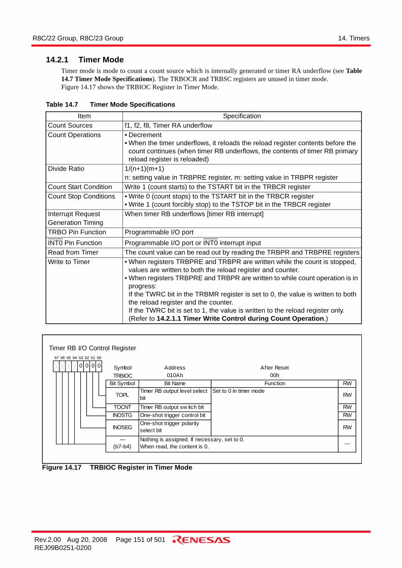
R8C/22 Group, R8C/23 Group 14. Timers
Rev.2.00 Aug 20, 2008 Page 151 of 501REJ09B0251-0200
14.2.1 Timer ModeTimer mode is mode to count a count source which is internally generated or timer RA underflow (see Table14.7 Timer Mode Specifications). The TRBOCR and TRBSC registers are unused in timer mode.Figure 14.17 shows the TRBIOC Register in Timer Mode.
Figure 14.17 TRBIOC Register in Timer Mode
Table 14.7 Timer Mode SpecificationsItem Specification
Count Sources f1, f2, f8, Timer RA underflowCount Operations • Decrement
• When the timer underflows, it reloads the reload register contents before the count continues (when timer RB underflows, the contents of timer RB primary reload register is reloaded)
Divide Ratio 1/(n+1)(m+1)n: setting value in TRBPRE register, m: setting value in TRBPR register
Count Start Condition Write 1 (count starts) to the TSTART bit in the TRBCR registerCount Stop Conditions • Write 0 (count stops) to the TSTART bit in the TRBCR register
• Write 1 (count forcibly stop) to the TSTOP bit in the TRBCR registerInterrupt Request Generation Timing
When timer RB underflows [timer RB interrupt]
TRBO Pin Function Programmable I/O portINT0 Pin Function Programmable I/O port or INT0 interrupt inputRead from Timer The count value can be read out by reading the TRBPR and TRBPRE registersWrite to Timer • When registers TRBPRE and TRBPR are written while the count is stopped,
values are written to both the reload register and counter.• When registers TRBPRE and TRBPR are written to while count operation is in
progress:If the TWRC bit in the TRBMR register is set to 0, the value is written to both the reload register and the counter.If the TWRC bit is set to 1, the value is written to the reload register only.(Refer to 14.2.1.1 Timer Write Control during Count Operation.)
Timer RB I/O Control Register
Symbol Address After ResetTRBIOC 010Ah 00h
Bit Symbol Bit Name Function RW
0
TOPLTimer RB output level selectbitTimer RB output sw itch bit
b7 b6 b5 b4 b3 b2
INOSEG
b1 b0
0 0
INOSTGTOCNT
0
Nothing is assigned. If necessary, set to 0.When read, the content is 0.
One-shot trigger polarityselect bit
—(b7-b4) —
Set to 0 in timer modeRW
RWRW
RW
One-shot trigger control bit

R8C/22 Group, R8C/23 Group 14. Timers
Rev.2.00 Aug 20, 2008 Page 152 of 501REJ09B0251-0200
14.2.1.1 Timer Write Control during Count OperationTimer RB has a prescaler and a timer (which counts the prescaler underflows). The prescaler and timer eachconsist of a reload register and a counter. In timer mode, the TWRC bit in the TRBMR register can be used toselect whether writing to the prescaler or timer during count operation is performed to both the reload registerand counter or only to the reload register.However, values are transferred from the reload register to the counter of the prescaler in synchronization withthe count source. In addition, values are transferred from the reload register to the counter of the timer insynchronization with prescaler underflows. Therefore, even if the TWRC bit is set for writing to both the reloadregister and counter, the counter value is not updated immediately after the WRITE instruction is executed. Inaddition, if the TWRC bit is set for writing to the reload register only, the synchronization of the writing will beshifted if the prescaler value changes.Figure 14.18 shows an Operating Example of Timer RB when Counter Value is Rewritten during CountOperation.

R8C/22 Group, R8C/23 Group 14. Timers
Rev.2.00 Aug 20, 2008 Page 153 of 501REJ09B0251-0200
Figure 14.18 Operating Example of Timer RB when Counter Value is Rewritten during Count Operation
Count source
Reloads register oftimer RB prescaler
IR bit in TRBICregister 0
Counter oftimer RB prescaler
Reloads register oftimer RB
Counter of timer RB
Set 01h to the TRBPRE register and 25h tothe TRBPR register by a program.
After writing, the reload register iswritten with the first count source.
Reload withthe secondcount source
Reload onunderflow
After writing, the reload register iswritten on the first underflow.
Reload on the secondunderflow
The IR bit remains unchanged until underflowis generated by a new value.
When the TWRC bit is set to 0 (write to reload register and counter)
Count source
Reloads register oftimer RB prescaler
IR bit in TRBICregister
Counter oftimer RB prescaler
Reloads register oftimer RB
Counter of timer RB
Set 01h to the TRBPRE register and 25h tothe TRBPR register by a program.
After writing, the reload register iswritten with the first count source.
Reload onunderflow
After writing, the reload register iswritten on the first underflow.
Reload onunderflow
Only the prescaler values are updated,extending the duration until timer RB underflow.
When the TWRC bit is set to 1 (write to reload register only)
05h 04h 03h 02h 01h 00h 01h 00h 01h 00h06h 01h 00h 01h
03h 00h02h 01h 25h
New value (25h)Previous value
New value (01h)Previous value
New value (01h)Previous value
05h 04h 01h 00h 01h 00h 01h 00h 01h 00h06h
New value (25h)Previous value
03h 24h02h 25h
The above applies under the following conditions.Both bits TSTART and TCSTF in the TRBCR register are set to 1 (During count).
0

R8C/22 Group, R8C/23 Group 14. Timers
Rev.2.00 Aug 20, 2008 Page 154 of 501REJ09B0251-0200
14.2.2 Programmable Waveform Generation ModeProgrammable waveform generation mode is mode to invert the signal output from the TRBO pin each time thecounter underflows, while the values in the TRBPR and TRBSC registers are counted alternately (see Table14.8 Programmable Waveform Generation Mode Specifications). A counting starts by counting the settingvalue in the TRBPR register. The TRBOCR register is unused in this mode.Figure 14.19 shows the TRBIOC Register in Programmable Waveform Generation Mode. Figure 14.20 showsthe Operation Example of Timer RB in Programmable Waveform Generation Mode.
NOTES:1. Even when counting the secondary period, read out the TRBPR register.2. The set values are reflected to the waveform output beginning with the following primary period after
writing to the TRBPR register.3. The value written to the TOCNT bit is enabled by the following.
• When count starts.• When the timer RB interrupt request is generated.
The contents after the TOCNT bit is changed are reflected from the output of the followingprimary period.
Table 14.8 Programmable Waveform Generation Mode SpecificationsItem Specification
Count Sources f1, f2, f8, timer RA underflowCount Operations • Decrement
• When the timer underflows, it reloads the contents of the primary reload and secondary reload registers alternately before the count continues.
Width and Period of Output Waveform
Primary period: (n+1)(m+1)/fiSecondary period: (n+1)(p+1)/fiPeriod: (n+1)(m+1)+(p+1)/fifi: Count source frequencyn: Setting value in TRBPRE registerm: Setting value in TRBPR registerp: Setting value in TRBSC register
Count Start Condition Write 1 (count start) to the TSTART bit in the TRBCR registerCount Stop Conditions
• Write 0 (count stop) to the TSTART bit in the TRBCR register• Write 1 (count forcibly stop) to the TSTOP bit in the TRBCR register
Interrupt Request Generation Timing
In half of count source, after timer RB underflows during secondary period (at the same time as the TRBO output change) [timer RB interrupt]
TRBO Pin Function Programmable output port or pulse outputINT0 Pin Function Programmable I/O port or INT0 interrupt inputRead from Timer The count value can be read out by reading the TRBPR and TRBPRE registers(1)
Write to Timer • When registers TRBPRE, TRBSC, and TRBPR are written while the count is stopped, values are written to both the reload register and counter.
• When registers TRBPRE, TRBSC, and TRBPR are written to during count operation, values are written to the reload registers only.(2)
Select Functions • Output level select functionThe TOPL bit can select the output level during primary and secondary periods.
• TRBO pin output switch functionTimer RB pulse output or P3_1 latch output is selected by the TOCNT bit in the TRBIOC register.(3)

R8C/22 Group, R8C/23 Group 14. Timers
Rev.2.00 Aug 20, 2008 Page 155 of 501REJ09B0251-0200
Figure 14.19 TRBIOC Register in Programmable Waveform Generation Mode
Timer RB I/O Control Register
Symbol Address After ResetTRBIOC 010Ah 00h
Bit Symbol Bit Name Function RW
b3 b2
INOSEG
b1 b0
INOSTG
b7 b6 b5 b4
RW
TOCNT RW
0 0
TOPL
Timer RB output level selectbit
0 : Outputs “H” for primary period Outputs “L” for secondary period Outputs “L” w hen the timer is stopped1 : Outputs “L” for primary period Outputs “H” for secondary period Outputs “H” w hen the timer is stopped
Timer RB output sw itch bit 0 : Outputs timer RB w aveform1 : Outputs value in P3_1 port latch
RW
RW
One-shot trigger control bit
Nothing is assigned. If necessary, set to 0.When read, the content is 0.
One-shot trigger polarityselect bit
—(b7-b4) —
Set to 0 in programmable w aveform generationmode
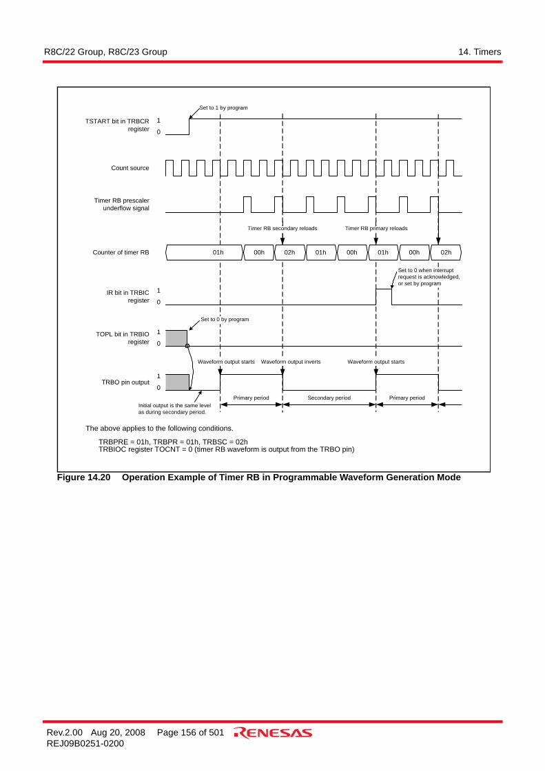
R8C/22 Group, R8C/23 Group 14. Timers
Rev.2.00 Aug 20, 2008 Page 156 of 501REJ09B0251-0200
Figure 14.20 Operation Example of Timer RB in Programmable Waveform Generation Mode
1
0
1
0
IR bit in TRBICregister
1
0
Count source
Timer RB prescalerunderflow signal
Counter of timer RB
TRBO pin output
TOPL bit in TRBIOregister
Set to 1 by program
Set to 0 when interruptrequest is acknowledged,or set by program
The above applies to the following conditions.
TSTART bit in TRBCRregister
1
0
01h 00h 02h
Timer RB secondary reloads Timer RB primary reloads
Set to 0 by program
TRBPRE = 01h, TRBPR = 01h, TRBSC = 02hTRBIOC register TOCNT = 0 (timer RB waveform is output from the TRBO pin)
02h 01h 00h 01h 00h
Primary period Primary periodSecondary period
Waveform output starts Waveform output inverts Waveform output starts
Initial output is the same levelas during secondary period.

R8C/22 Group, R8C/23 Group 14. Timers
Rev.2.00 Aug 20, 2008 Page 157 of 501REJ09B0251-0200
14.2.3 Programmable One-shot Generation ModeProgrammable one-shot generation mode is mode to output the one-shot pulse from the TRBO pin by aprogram or an external trigger input (input to the INT0 pin) (see Table 14.9 Programmable One-ShotGeneration Mode Specifications). When a trigger is generated, the timer starts operating from the point onlyonce for a given period equal to the set value in the TRBPR register. The TRBSC register is unused in thismode.Figure 14.21 shows the TRBIOC Register in Programmable One-Shot Generation Mode. Figure 14.22 showsthe Operation Example of Programmable One-Shot Generation Mode.
NOTES:1. The set value is reflected at the following one-shot pulse after writing to the TRBPR register.2. Do not set both the TRBPRE and TRBPR registers to 00h.
Table 14.9 Programmable One-Shot Generation Mode SpecificationsItem Specification
Count Sources f1, f2, f8, timer RA underflowCount Operations • Decrement the setting value in the TRBPR register
• When the timer underflows, it reloads the contents of the reload register before the count completes and the TOSSTF bit is set to 0 (one-shot stops).
• When a count stops, the timer reloads the contents of the reload register before it stops.
One-Shot Pulse Output Time
(n+1)(m+1)/fifi: Count source frequency,n: Setting value in TRBPRE register, m: Setting value in TRBPR register(2)
Count Start Conditions
• The TSTART bit in the TRBCR register is set to 1 (count starts) and the next trigger is generated.
• Set the TOSST bit in the TRBOCR register to 1 (one-shot starts)• Input trigger to the INT0 pin
Count Stop Conditions
• When reloading completes after Timer RB underflows during primary period.• When the TOSSP bit in the TRBOCR register is set to 1 (one-shot stops) • When the TSTART bit in the TRBCR register is set to 0 (stops counting)• When the TSTOP bit in the TRBCR register is set to 1 (forcibly stops counting)
Interrupt Request Generation Timing
In half cycles of count source, after the timer underflows (at the same time as the TRBO output ends) [timer RB interrupt]
TRBO Pin Function Pulse outputINT0 Pin Functions • When the INOSTG bit in the TRBIOC register is set to 0 (INT0 one-shot trigger
disabled), programmable I/O port or INT0 interrupt input• When the INOSTG bit in the TRBIOC register is set to 1 (INT0 one-shot trigger
enabled), external trigger (INT0 interrupt input)Read from Timer The count value can be read out by reading the TRBPR and TRBPRE registers.Write to Timer • When registers TRBPRE and TRBPR are written while the count is stopped,
values are written to both the reload register and counter. • When registers TRBPRE and TRBPR are written during the count, values are
written to the reload register only (the data is transferred to the counter at the following reload)(1).
Select Functions • Output level select functionThe TOPL bit in the TRBIOC register can select the output level of the one-shot pulse waveform.
• One-shot trigger select functionRefer to 14.2.3.1 One-Shot Trigger Selection.

R8C/22 Group, R8C/23 Group 14. Timers
Rev.2.00 Aug 20, 2008 Page 158 of 501REJ09B0251-0200
Figure 14.21 TRBIOC Register in Programmable One-Shot Generation Mode
Timer RB I/O Control Register
Symbol Address After ResetTRBIOC 010Ah 00h
Bit Symbol Bit Name Function RW
0 : INT0_____
pin one-shot trigger disabled1 : INT0
_____ pin one-shot trigger enabled
NOTE:1.
RW
RW
One-shot trigger control bit(1)
0 : Falling edge trigger1 : Rising edge trigger
RW
TOCNT RW
TOPL
Timer RB output level selectbit
0 : Outputs one-shot pulse “H” Outputs “L” w hen the timer is stopped1 : Outputs one-shot pulse “L” Outputs “H” w hen the timer is stopped
Timer RB output sw itch bit Set to 0 in programmable one-shot generationmode
b7 b6 b5 b4 b3 b2
INOSEG
b1 b0
0
INOSTG
Nothing is assigned. If necessary, set to 0.When read, the content is 0.
One-shot trigger polarityselect bit(1)
—(b7-b4) —
Refer to 14.2.3.1 One-shot Trigger Selection.
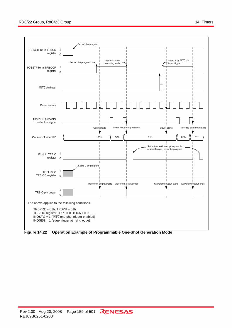
R8C/22 Group, R8C/23 Group 14. Timers
Rev.2.00 Aug 20, 2008 Page 159 of 501REJ09B0251-0200
Figure 14.22 Operation Example of Programmable One-Shot Generation Mode
TOSSTF bit in TRBOCRregister
INT0 pin input
1
0
1
0
IR bit in TRBICregister
1
0
Count source
Timer RB prescalerunderflow signal
Counter of timer RB
TRBIO pin output
TOPL bit inTRBIOC register
Set to 1 by program
Set to 1 by program
Set to 0 when interrupt request isacknowledged, or set by program
The above applies to the following conditions.
TSTART bit in TRBCRregister
1
0
1
0
01h 00h 01h 00h 01h
Count starts Timer RB primary reloads Count starts Timer RB primary reloads
Set to 0 by program
Waveform output starts Waveform output ends Waveform output starts Waveform output ends
Set to 0 whencounting ends
Set to 1 by INT0 pininput trigger
TRBPRE = 01h, TRBPR = 01hTRBIOC register TOPL = 0, TOCNT = 0INOSTG = 1 (INT0 one-shot trigger enabled)INOSEG = 1 (edge trigger at rising edge)

R8C/22 Group, R8C/23 Group 14. Timers
Rev.2.00 Aug 20, 2008 Page 160 of 501REJ09B0251-0200
14.2.3.1 One-Shot Trigger SelectionIn programmable one-shot generation mode and programmable wait one-shot generation mode, operation startswhen a one-shot trigger is generated while the TCSTF bit in the TRBCR register is set to 1 (count starts).A one-shot trigger can be generated by either of the following causes:
• 1 is written to the TOSST bit in the TRBOCR register by a program.• Trigger input from the INT0 pin.
When a one-shot trigger occurs, the TOSSTF bit in the TRBOCR register is set to 1 (one-shot operation inprogress) after one or two cycles of the count source have elapsed. Then, in programmable one-shot generationmode, count operation begins and one-shot waveform output starts. (In programmable wait one-shot generationmode, count operation starts for the wait period.) If a one-shot trigger occurs while the TOSSTF bit is set to 1,no retriggering occurs.
To use trigger input from the INT0 pin, input the trigger after making the following settings:• Set the PD4_5 bit in the PD4 register to 0 (input port).• Select the INT0 digital filter with bits INT0F1 and INT0F0 in the INTF register.• Select both edges or one edge with the INT0PL bit in INTEN register. If one edge is selected, further select
falling or rising edge with the INOSEG bit in TRBIOC register.• Set the INT0EN bit in the INTEN register to 0 (enabled).• After completing the above, set the INOSTG bit in the TRBIOC register to 1 (INT pin one-shot trigger
enabled).
Note the following points with regard to generating interrupt requests by trigger input from the INT0 pin.• Processing to handle the interrupts is required. Refer to 12. Interrupts for details.• If one edge is selected, use the POL bit in the INT0IC register to select falling or rising edge. (The
INOSEG bit in the TRBIOC register does not affect INT0 interrupts).• If a one-shot trigger occurs while the TOSSTF bit is set to 1, timer RB operation is not affected, but the
value of the IR bit in the INT0IC register changes.

R8C/22 Group, R8C/23 Group 14. Timers
Rev.2.00 Aug 20, 2008 Page 161 of 501REJ09B0251-0200
14.2.4 Programmable Wait One-shot Generation ModeProgrammable wait one-shot generation mode is mode to output the one-shot pulse from the TRBO pin by aprogram or an external trigger input (input to the INT0 pin) (see Table 14.10 Programmable Wait One-ShotGeneration Mode Specifications). When a trigger is generated from this point, the timer starts outputtingpulses only once for a given length of time equal to the setting value in the TRBSC register after waiting for agiven length of time equal to the setting value in the TRBPR register.Figure 14.23 shows the TRBIOC Register in Programmable Wait One-Shot Generation Mode. Figure 14.24shows the Operation Example of Programmable Wait One-Shot Generation Mode.

R8C/22 Group, R8C/23 Group 14. Timers
Rev.2.00 Aug 20, 2008 Page 162 of 501REJ09B0251-0200
NOTES:1. The set value is reflected at the following one-shot pulse after writing to registers TRBSC and
TRBPR.2. Do not set both the TRBPRE and TRBPR registers to 00h.
Table 14.10 Programmable Wait One-Shot Generation Mode SpecificationsItem Specification
Count Sources f1, f2, f8, timer RA underflowCount Operations • Decrement the setting value in timer RB primary
• When a count of timer RB primary underflows, the timer reloads the contents of the timer RB secondary before the count continues.
• When a count of timer RB secondary underflows, the timer reloads the contents of the timer RB primary before the count completes and the TOSSTF bit is set to 0 (one-shot stops).
• When a count stops, the timer reloads the contents of the reload register before it stops.
Wait Time (n+1)(m+1)/fifi: Count source frequencyn: Setting value in the TRBPRE register, m: Setting value in the TRBPR register(2)
One-Shot Pulse Output Time (n+1)(p+1)/fifi: Count source frequencyn: Setting value in the TRBPRE register, p: Setting value in the TRBSC register
Count Start Conditions • The TSTART bit in the TRBCR register is set to 1 (count starts) and the next trigger is generated.
• Set the TOSST bit in the TRBOCR register to 1 (one-shot starts)• Input trigger to the INT0 pin
Count Stop Conditions • When reloading completes after timer RB underflows during secondary period• When the TOSSP bit in the TRBOCR register is set to 1 (one-shot stops)• When the TSTART bit in the TRBCR register is set to 0 (starts counting)• When the TSTOP bit in the TRBCR register is set to 1 (forcibly stops
counting)Interrupt Request Generation Timing
In half cycles of the count source after timer RB underflows during secondary period (complete at the same time as waveform output from the TRBO pin) [timer RB interrupt]
TRBO Pin Function Pulse outputINT0 Pin Functions • When the INOSTG bit in the TRBIOC register is set to 0 (INT0 one-shot
trigger disabled), programmable I/O port or INT0 interrupt input• When the INOSTG bit in the TRBIOC register is set to 1 (INT0 one-shot
trigger enabled), external trigger (INT0 interrupt input)Read from Timer The count value can be read out by reading the TRBPR and TRBPRE
registers.Write to Timer • When registers TRBPRE, TRBSC, and TRBPR are written while the
count stops, values are written to both the reload register and counter.• When registers TRBPRE, TRBSC, and TRBPR are written to during
count operation, values are written to the reload registers only.(1)
Select Functions • Output level select functionThe TOPL bit in the TRBIO register can select the output level of the one-shot pulse waveform.
• One-shot trigger select functionRefer to 14.2.3.1 One-Shot Trigger Selection.

R8C/22 Group, R8C/23 Group 14. Timers
Rev.2.00 Aug 20, 2008 Page 163 of 501REJ09B0251-0200
Figure 14.23 TRBIOC Register in Programmable Wait One-Shot Generation Mode
Timer RB I/O Control Register
Symbol Address After ResetTRBIOC 010Ah 00h
Bit Symbol Bit Name Function RW
0 : INT0_____
pin one-shot trigger disabled1 : INT0
_____ pin one-shot trigger enabled
NOTE:1.
Nothing is assigned. If necessary, set to 0.When read, the content is 0.
One-shot trigger polarityselect bit(1)
—(b7-b4) —
Refer to 14.2.3.1 One-shot Trigger Selection.
b3 b2
INOSEG
b1 b0
0
INOSTG
b7 b6 b5 b4
RW
TOCNT RW
TOPL
Timer RB output level selectbit
0 : Outputs one-shot pulse “H” Outputs “L” w hen the timer is stopped or during w ait1 : Outputs one-shot pulse “L” Outputs “H” w hen the timer is stopped or during w ait
Timer RB output sw itch bit Set to 0 in programmable w ait one-shot generationmode
RW
RW
One-shot trigger control bit(1)
0 : Falling edge trigger1 : Rising edge trigger

R8C/22 Group, R8C/23 Group 14. Timers
Rev.2.00 Aug 20, 2008 Page 164 of 501REJ09B0251-0200
Figure 14.24 Operation Example of Programmable Wait One-Shot Generation Mode
TOSSTF bit in TRBOCRregister
INT0 pin input
1
0
1
0
IR bit in TRBICregister
1
0
Count source
Timer RB prescalerunderflow signal
Counter of timer RB
TRBIO pin output
TOPL bit inTRBIOC register
Set to 1 by program
Set to 1 by setting 1 to TOSST bit in TRBOCRregister, or INT0 pin input trigger
Set to 0 when interrupt request isacknowledged, or set by program
The above applies to the following conditions.
TSTART bit in TRBCRregister
1
0
1
0
01h 00h 00h 01h
Count starts Timer RB secondary reloads Timer RB primary reloads
Set to 0 by program
Wait starts Waveform output starts Waveform output ends
Set to 0 whencounting ends
TRBPRE = 01h, TRBPR = 01h, TRBSC = 04hINOSTG = 1 (INT0 one-shot trigger enabled)INOSEG = 1 (edge trigger at rising edge)
04h 03h 02h 01h
Wait(primary period)
One-shot pulse(secondary period)

R8C/22 Group, R8C/23 Group 14. Timers
Rev.2.00 Aug 20, 2008 Page 165 of 501REJ09B0251-0200
14.2.5 Notes on Timer RB• Timer RB stops counting after reset. Set the value to timer RB and timer RB prescaler before the count
starts.• Even if the prescaler and timer RB is read out in 16-bit units, these registers are read by 1 byte in the MCU.
Consequently, the timer value may be updated during the period these two registers are being read.• In programmable one-shot generation mode and programmable wait one-shot generation mode, when
setting the TSTART bit in the TRBCR register to 0, 0 (stops counting) or setting the TOSSP bit in theTRBOCR register to 1 (stops one-shot), the timer reloads the value of reload register and stops. Therefore,read the timer count value in programmable one-shot generation mode and programmable wait one-shotgeneration mode before the timer stops.
• The TCSTF bit retains 0 (count stops) for 1 to 2 cycles of the count source after setting the TSTART bit to1 (count starts) while the count stops.During this time, do not access registers associated with timer RB(1) other than the TCSTF bit.The TCSTF bit retains 1 for 1 to 2 cycles of the count source after setting the TSTART bit to 0 (countstops) while the count is performing. Timer RB counting is stopped when the TCSTF bit is set to 0.During this time, do not access registers associated with timer RB(1) other than the TCSTF bit.
NOTE:1. Registers associated with timer RB: TRBCR, TRBOCR, TRBIOC, TRBMR, TRBPRE, TRBSC, TRBPR
• If the TSTOP bit in the TRBCR register is set to 1 during timer operation, timer RB stops immediately.• If 1 is written to the TOSST or TOSSP bit in the TRBOCR register, the value of the TOSSTF bit changes
after one or two cycles of the count source have elapsed. If the TOSSP bit is written to 1 during the periodbetween when the TOSST bit is written to 1 and when the TOSSTF bit is set to 1, the TOSSTF bit may beset to either 0 or 1 depending on the content state. Likewise, if the TOSST bit is written to 1 during theperiod between when the TOSSP bit is written to 1 and when the TOSSTF bit is set to 0, the TOSSTF bitmay be set to either 0 or 1.
14.2.5.1 Timer modeThe following workaround should be performed in timer mode. To write to registers TRBPRE and TRBPR during count operation (TCSTF bit is set to 1), note the followingpoints:
• When the TRBPRE register is written continuously, allow three or more cycles of the count source for eachwrite interval.
• When the TRBPR register is written continuously, allow three or more cycles of the prescaler underflowfor each write interval.

R8C/22 Group, R8C/23 Group 14. Timers
Rev.2.00 Aug 20, 2008 Page 166 of 501REJ09B0251-0200
14.2.5.2 Programmable waveform generation modeThe following three workarounds should be performed in programmable waveform generation mode.
(1) To write to registers TRBPRE and TRBPR during count operation (TCSTF bit is set to 1), note thefollowing points:
• When the TRBPRE register is written continuously, allow three or more cycles of the count source for eachwrite interval.
• When the TRBPR register is written continuously, allow three or more cycles of the prescaler underflowfor each write interval.
(2) To change registers TRBPRE and TRBPR during count operation (TCSTF bit is set to 1), synchronizethe TRBO output cycle using a timer RB interrupt, etc. This operation should be preformed only once inthe same output cycle. Also, make sure that writing to the TRBPR register does not occur during periodA shown in Figures 14.25 and 14.26.
The following shows the detailed workaround examples.• Workaround example (a):
As shown in Figure 14.25, write to registers TRBSC and TRBPR in the timer RB interrupt routine. Thesewrite operations must be completed by the beginning of period A.
Figure 14.25 Workaround Example (a) When Timer RB Interrupt is Used
TRBO pin output
Count source/prescaler
underflow signal
Primary period
Period A
IR bit inTRBIC register
Secondary period
(b)
Interruptsequence
Instruction ininterrupt routine
Interrupt request isacknowledged
(a)
Interrupt requestis generated
Ensure sufficient time
Set the secondary and thenthe primary register immediately
(a) Period between interrupt request generation and the completion of execution of an instruction. The length of timevaries depending on the instruction being executed.The DIVX instruction requires the longest time, 30 cycles (assuming no wait states and that a register is set asthe divisor).
(b) 20 cycles. 21 cycles for address match and single-step interrupts.

R8C/22 Group, R8C/23 Group 14. Timers
Rev.2.00 Aug 20, 2008 Page 167 of 501REJ09B0251-0200
• Workaround example (b): As shown in Figure 14.26 detect the start of the primary period by the TRBO pin output level and write toregisters TRBSC and TRBPR. These write operations must be completed by the beginning of period A.If the port register’s bit value is read after the port direction register’s bit corresponding to the TRBO pin isset to 0 (input mode), the read value indicates the TRBO pin output value.
Figure 14.26 Workaround Example (b) When TRBO Pin Output Value is Read
(3) To stop the timer counting in the primary period, use the TSTOP bit in the TRBCR register. In this case,registers TRBPRE and TRBPR are initialized and their values are set to the values after reset.
14.2.5.3 Programmable one-shot generation modeThe following two workarounds should be performed in programmable one-shot generation mode.
(1) To write to registers TRBPRE and TRBPR during count operation (TCSTF bit is set to 1), note thefollowing points:
• When the TRBPRE register is written continuously during count operation (TCSTF bit is set to 1), allowthree or more cycles of the count source for each write interval.
• When the TRBPR register is written continuously during count operation (TCSTF bit is set to 1), allowthree or more cycles of the prescaler underflow for each write interval.
(2) Do not set both the TRBPRE and TRBPR registers to 00h.
TRBO pin output
Count source/prescaler
underflow signal
Primary period
Period A
Read value of the port register’sbit corresponding to the TRBO pin
(when the bit in the port directionregister is set to 0)
Secondary period
(i)
The TRBO output inversionis detected at the end of the
secondary period.
Ensure sufficient time
Upon detecting (i), set the secondary andthen the primary register immediately.
(ii) (iii)

R8C/22 Group, R8C/23 Group 14. Timers
Rev.2.00 Aug 20, 2008 Page 168 of 501REJ09B0251-0200
14.2.5.4 Programmable wait one-shot generation modeThe following three workarounds should be performed in programmable wait one-shot generation mode.
(1) To write to registers TRBPRE and TRBPR during count operation (TCSTF bit is set to 1), note thefollowing points:
• When the TRBPRE register is written continuously, allow three or more cycles of the count source for eachwrite interval.
• When the TRBPR register is written continuously, allow three or more cycles of the prescaler underflowfor each write interval.
(2) Do not set both the TRBPRE and TRBPR registers to 00h.
(3) Set registers TRBSC and TRBPR using the following procedure.(a) To use “INT0 pin one-shot trigger enabled” as the count start condition
Set the TRBSC register and then the TRBPR register. At this time, after writing to the TRBPRregister, allow an interval of 0.5 or more cycles of the count source before trigger input from theINT0 pin.
(b) To use “writing 1 to TOSST bit” as the start conditionSet the TRBSC register, the TRBPR register, and then TOSST bit. At this time, after writing to theTRBPR register, allow an interval of 0.5 or more cycles of the count source before writing to theTOSST bit.

R8C/22 Group, R8C/23 Group 14. Timers
Rev.2.00 Aug 20, 2008 Page 169 of 501REJ09B0251-0200
14.3 Timer RDTimer RD has 2 16-bit timers (channels 0 and 1). Each channel has 4 I/O pins.The operation clock of Timer RD is f1 or fOCO40M.Table 14.11 lists the Timer RD Operation Clocks.
Figure 14.27 shows the Block Diagram of Timer RD. Timer RD has 5 modes:• Timer mode
- Input capture function Transfer the counter value to a register as a trigger of the external signal- Output compare function Detect the register value match with a counter
(Pin output can be changed at detection)
The following 4 modes using the output compare function.• PWM mode Output any-wide pulse continuously• Reset synchronous PWM mode Output three-phase waveforms (6) without sawtooth
wave modulation and dead time• Complementary PWM mode Output three-phase waveforms (6) with triangular
wave modulation and dead time• PWM3 mode Output PWM waveform (2) with same period
In the input capture function, output compare function and PWM mode, Channels 0 and 1 have the equivalentfunctions, and functions or modes can be selected every pin. Also, a combination of these functions and modes canbe used in 1 channel.In reset synchronous PWM mode, complementary PWM mode and PWM3 mode, a waveform is output with acombination of counters and registers in Channels 0 and 1.
Tables 14.12 to 14.20 lists the Pin Functions of timer RD.
Table 14.11 Timer RD Operation ClocksCondition Operation Clock of Timer RD
The count source is f1, f2, f4, f8, f32 and TRDCLK input.(The TCK2 to TCK0 bits in the TRDCR0 and TRDCR1 registers are set to 000b to 101b.)
f1
The count source is fOCO40M. (The TCK2 to TCK0 bits in the TRDCR0 and TRDCR1 registers are set to 110b.)
fOCO40M

R8C/22 Group, R8C/23 Group 14. Timers
Rev.2.00 Aug 20, 2008 Page 170 of 501REJ09B0251-0200
X: can be 0 or 1, no change in outcomeNOTE:
1. Set the PD2_0 bit in the PD2 register to 0 (input mode) at timer mode trigger input (input capture function) and external clock input (TRDCLK).
X: can be 0 or 1, no change in outcomeNOTE:
1. Set the PD2_1 bit in the PD2 register to 0 (input mode) at timer mode trigger input (input capture function).
X: can be 0 or 1, no change in outcomeNOTE:
1. Set the PD2_2 bit in the PD2 register to 0 (input mode) at timer mode trigger input (input capture function).
Table 14.12 Pin Functions TRDIOA0/TRDCLK(P2_0)Register TRDOER1 TRDFCR TRDIORA0
FunctionBit EA0 PWM3 STCLK CMD1, CMD0 IOA3 IOA2_IOA0
Setting value
0 0 0 00b X XXXb PWM3 mode waveform output
0 1 0 00b 1 001b, 01Xb Timer mode waveform output (output compare function)
X1 0 00b X 1XXb Timer mode trigger input (input capture function)(1)
1 1 XXb X 000b External clock input (TRDCLK)(1)
Other than above I/O port
Table 14.13 Pin Functions TRDIOB0(P2_1)Register TRDOER1 TRDFCR TRDPMR TRDIORA0
FunctionBit EB0 PWM3 CMD1, CMD0 PWMB0 IOB2_IOB0
Setting value
0 X 1Xb X XXXb Complementary PWM mode waveform output
0 X 01b X XXXb Reset synchronous PWM mode waveform output
0 0 00b X XXXb PWM3 mode waveform output
0 1 00b 1 XXXb PWM mode waveform output
0 1 00b 0 001b, 01Xb Timer mode waveform output (output compare function)
X 1 00b 0 1XXb Timer mode trigger input (input capture function)(1)
Other than above I/O port
Table 14.14 Pin Functions TRDIOC0(P2_2)Register TRDOER1 TRDFCR TRDPMR TRDIORC0
FunctionBit EC0 PWM3 CMD1, CMD0 PWMC0 IOC2_IOC0
Setting value
0 X 1Xb X XXXb Complementary PWM mode waveform output
0 X 01b X XXXb Reset synchronous PWM mode waveform output
0 1 00b 1 XXXb PWM mode waveform output
0 1 00b 0 001b, 01Xb Timer mode waveform output (output compare function)
X 1 00b 0 1XXb Timer mode trigger input (input capture function)(1)
Other than above I/O port

R8C/22 Group, R8C/23 Group 14. Timers
Rev.2.00 Aug 20, 2008 Page 171 of 501REJ09B0251-0200
X: can be 0 or 1, no change in outcomeNOTE:
1. Set the PD2_3 bit in the PD2 register to 0 (input mode) at timer mode trigger input (input capture function).
X: can be 0 or 1, no change in outcomeNOTE:
1. Set the PD2_4 bit in the PD2 register to 0 (input mode) at timer mode trigger input (input capture function).
X: can be 0 or 1, no change in outcomeNOTE:
1. Set the PD2_5 bit in the PD2 register to 0 (input mode) at timer mode trigger input (input capture function).
Table 14.15 Pin Functions TRDIOD0(P2_3)Register TRDOER1 TRDFCR TRDPMR TRDIORC0
FunctionBit ED0 PWM3 CMD1, CMD0 PWMD0 IOD2_IOD0
Setting value
0 X 1Xb X XXXb Complementary PWM mode waveform output
0 X 01b X XXXb Reset synchronous PWM mode waveform output
0 1 00b 1 XXXb PWM mode waveform output
0 1 00b 0 001b, 01Xb Timer mode waveform output (output compare function)
X 1 00b 0 1XXb Timer mode trigger input (input capture function)(1)
Other than above I/O port
Table 14.16 Pin Functions TRDIOA1(P2_4)Register TRDOER1 TRDFCR TRDIORA1
FunctionBit EA1 PWM3 CMD1, CMD0 IOA2_IOA0
Setting value
0 X 1Xb XXXb Complementary PWM mode waveform output
0 X 01b XXXb Reset synchronous PWM mode waveform output
0 1 00b 001b, 01Xb Timer mode waveform output (output compare function)
X 1 00b 1XXb Timer mode trigger input (input capture function)(1)
Other than above I/O port
Table 14.17 Pin Functions TRDIOB1(P2_5)Register TRDOER1 TRDFCR TRDPMR TRDIORA1
FunctionBit EB1 PWM3 CMD1, CMD0 PWMB1 IOB2_IOB0
Setting value
0 X 1Xb X XXXb Complementary PWM mode waveform output
0 X 01b X XXXb Reset synchronous PWM mode waveform output
0 1 00b 1 XXXb PWM mode waveform output
0 1 00b 0 001b, 01Xb Timer mode waveform output (output compare function)
X 1 00b 0 1XXb Timer mode trigger input (input capture function)(1)
Other than above I/O port

R8C/22 Group, R8C/23 Group 14. Timers
Rev.2.00 Aug 20, 2008 Page 172 of 501REJ09B0251-0200
X: can be 0 or 1, no change in outcomeNOTE:
1. Set the PD2_6 bit in the PD2 register to 0 (input mode) at timer mode trigger input (input capture function).
X: can be 0 or 1, no change in outcomeNOTE:
1. Set the PD2_7 bit in the PD2 register to 0 (input mode) at timer mode trigger input (input capture function).
X: can be 0 or 1, no change in outcome
Table 14.18 Pin Functions TRDIOC1(P2_6)Register TRDOER1 TRDFCR TRDPMR TRDIORC1
FunctionBit EC1 PWM3 CMD1, CMD0 PWMC1 IOC2_IOC0
Setting value
0 X 1Xb X XXXb Complementary PWM mode waveform output
0 X 01b X XXXb Reset synchronous PWM mode waveform output
0 1 00b 1 XXXb PWM mode waveform output
0 1 00b 0 001b, 01Xb Timer mode waveform output (output compare function)
X 1 00b 0 1XXb Timer mode trigger input (input capture function)(1)
Other than above I/O port
Table 14.19 Pin Functions TRDIOD1(P2_7)Register TRDOER1 TRDFCR TRDPMR TRDIORC1
FunctionBit ED1 PWM3 CMD1, CMD0 PWMD1 IOD2_IOD0
Setting value
0 X 1Xb X XXXb Complementary PWM mode waveform output
0 X 01b X XXXb Reset synchronous PWM mode waveform output
0 1 00b 1 XXXb PWM mode waveform output
0 1 00b 0 001b, 01Xb Timer mode waveform output (output compare function)
X 1 00b 0 1XXb Timer mode trigger input (input capture function)(1)
Other than above I/O port
Table 14.20 Pin Functions INT0(P4_5)Register TRDOER2 INTEN PD4
FunctionBit PTO INT0PL INT0EN PD4_5
Setting value
1 0 1 0 Pulse output forced cutoff signal input
Other than above I/O port or INT0 interrupt input
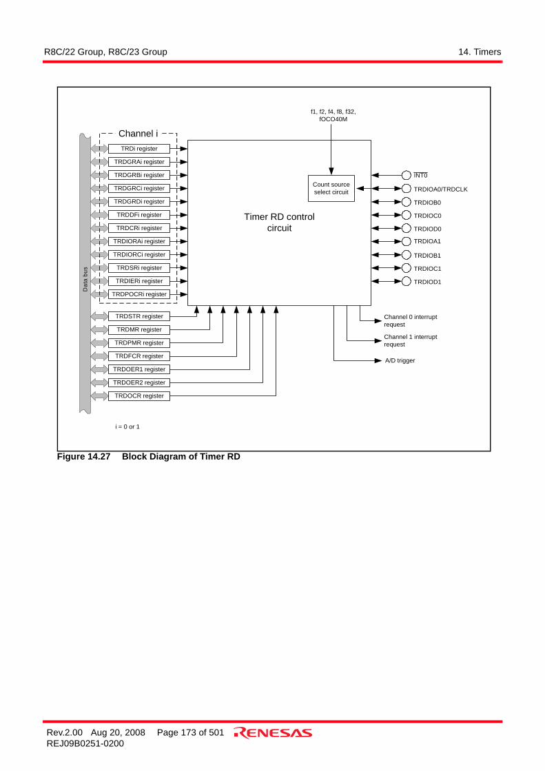
R8C/22 Group, R8C/23 Group 14. Timers
Rev.2.00 Aug 20, 2008 Page 173 of 501REJ09B0251-0200
Figure 14.27 Block Diagram of Timer RD
TRDi register
Dat
a bu
s
TRDGRAi register
TRDGRBi register
TRDGRCi register
TRDGRDi register
TRDCRi register
TRDIORAi register
TRDIORCi register
TRDSRi register
TRDIERi register
TRDPOCRi register
TRDSTR register
TRDMR register
TRDPMR register
TRDFCR register
TRDOER1 register
TRDOER2 register
TRDOCR register
Timer RD controlcircuit
INT0
TRDIOA0/TRDCLK
TRDIOB0
TRDIOC0
TRDIOD0
TRDIOB1
TRDIOC1
TRDIOD1
TRDIOA1
Count sourceselect circuit
f1, f2, f4, f8, f32,fOCO40M
Channel 0 interruptrequest
Channel 1 interruptrequest
A/D trigger
Channel i
i = 0 or 1
TRDDFi register

R8C/22 Group, R8C/23 Group 14. Timers
Rev.2.00 Aug 20, 2008 Page 174 of 501REJ09B0251-0200
14.3.1 Count SourceThe count source selection can be used in all modes. However, in PWM3 mode, the external clock cannot beselected.
i = 0 or 1NOTE:
1. The count source fOCO40M can be used with VCC = 3.0 to 5.5 V.
Figure 14.28 Block Diagram of Count Source
Set the pulse width of the external clock which inputs to the TRDCLK pin to 3 cycles or above of the operationclock of Timer RD (refer to Table 14.11 Timer RD Operation Clocks).When selecting fOCO40M for the count source, set the FRA00 bit in the FRA0 register to 1 (high-speed on-chip oscillator on) before setting the TCK2 to TCK0 bits in the TRDCRi register (i = 0 or 1) to 110b(fOCO40M).
Table 14.21 Count Source SelectionCount Source Selection
f1, f2, f4, f8, f32 The count source is selected by bits TCK2 to TCK0 in the TRDCRi register.fOCO40M(1) The FRA00 bit in the FRA0 register is set to 1 (high-speed on-chip oscillator
frequency).Bits TCK2 to TCK0 in the TRDCRi register is set to 110b (fOCO40M).
External Signal Input to TRDCLK Pin
The STCLK bit in the TRDFCR register is set to 1 (external clock input enabled).The TCK2 to TCK0 bits in the TRDCRi register are set to 101b (count source: external clock).The valid edge selected by the CKEG1 to CKEG0 bits in the TRDCRi register.The PD2_0 bit in the PD2 register is set to 0 (input mode).
TRDCLK/TRDIOA0
TCK2 to TCK0
TRDi register
i = 0 or 1
TCK2 to TCK0, CKEG1 to CKEG0: Bits in TRDCRi registerSTCLK: Bit in TRDFCR register
f1
f2
f4
f8
f32
= 001b
= 010b
= 011b
= 000b
= 101b
= 100b
Valid edgeselected
CKEG1 to CKEG0
TRDIOA0 I/O or programmable I/O port
Count source
STCLK = 1
STCLK = 0
fOCO40M = 110b

R8C/22 Group, R8C/23 Group 14. Timers
Rev.2.00 Aug 20, 2008 Page 175 of 501REJ09B0251-0200
14.3.2 Buffer OperationThe TRDGRCi register can be used as the buffer register of the TRDGRAi register, and the TRDGRDi registercan be used as the buffer register of the TRDGRBi register by the BFCi and BFDi bits in the TRDMR register.
• TRDGRAi buffer register: TRDGRCi register• TRDGRBi buffer register: TRDGRDi register
Buffer operation depends on modes. Table 14.22 lists the Buffer Operation in Each Mode.Figure 14.29 shows the Buffer Operation in Input Capture Function, and Figure 14.30 shows the BufferOperation in Output Compare Function.
i = 0 or 1
Figure 14.29 Buffer Operation in Input Capture Function
Table 14.22 Buffer Operation in Each ModeFunction and Mode Transfer Timing Transfer Register
Input Capture Function Input capture signal input Transfer content in TRDGRAi (TRDGRBi) register to buffer register
Output Compare Function Compare match with TRDi register and TRDGRAi (TRDGRBi) register
Transfer content in buffer register to TRDGRAi (TRDGRBi) registerPWM Mode
Reset Synchronous PWM Mode
Compare match withTRD0 register and TRDGRA0 register
Transfer content in buffer register to TRDGRAi (TRDGRBi) register
Complementary PWM Mode
• Compare match with TRD0 register and TRDGRA0 register
• TRD1 register underflow
Transfer content in buffer register to TRDGRB0, TRDGRA1 and TRDGRB1 registers
PWM3 Mode Compare match with TRD0 register and TRDGRA0 register
Transfer content in buffer register to TRDGRA0, TRDGRB0, TRDGRA1 and TRDGRB1 registers
m
Transfer
nTRDGRAi register
n-1 n+1
TRDIOAi input
TRDi register
i = 0 or 1
The above applies to the following conditions:• The BFCi bit in the TRDMR register is set to 1. (The TRDGRCi register is used as the buffer register of
the TRDGRAi register.)• The IOA2 to IOA0 bits in the TRDIORAi register are set to 100b (input capture at the falling edge).
m
TransferTRDGRCi register
(buffer)
n
TRDGRCiregister(buffer)
TRDGRAiregister TRDi
TRDIOAi input(input capture signal)

R8C/22 Group, R8C/23 Group 14. Timers
Rev.2.00 Aug 20, 2008 Page 176 of 501REJ09B0251-0200
Figure 14.30 Buffer Operation in Output Compare Function
Perform the following for the timer mode (input capture and output compare functions).When using the TRDGRCi (i = 0 or 1) register as the buffer register of the TRDGRAi register
• Set the IOC3 bit in the TRDIORCi register to 1 (general register or buffer register).• Set the IOC2 bit in the TRDIORCi register to the same as the IOA2 bit in the TRDIORAi register.
When using the TRDGRDi register as the buffer register of the TRDGRBi register• Set the IOD3 bit in the TRDIORDi register to 1 (general register or buffer register).• Set the IOD2 bit in the TRDIORCi register to the same value as the IOB2 bit in the TRDIORAi register.
Bits IMFC and IMFD in the TRDSRi register are set to 1 at the input edge of the TRDIOCi pin when also usingregisters TRDGRCi and TRDGRDi as the buffer register in the input capture function.
When using the TRDGRCi and TRDGRDi registers for the buffer register in output compare function, resetsynchronous PWM mode, complementary PWM mode and PWM3 mode, the IMFC and IMFD bits in theTRDSRi register are set to 1 by the compare match with the TRDi register.
m nTRDGRAi register
m-1 m+1TRDi register
i = 0 or 1
The above applies to the following conditions:• BFCi bit in the TRDMR register is set to 1. (The TRDGRCi register is used as the buffer register of
the TRDGRAi register.)• IOA2 to IOA0 bits in the TRDIORAi register are set to 001b (“L” output by the compare match).
n
TransferTRDGRCi register
(buffer)
m
TRDIOAi output
TRDGRCiregister(buffer)
TRDGRAiregister Comparator TRDi
Compare match signal

R8C/22 Group, R8C/23 Group 14. Timers
Rev.2.00 Aug 20, 2008 Page 177 of 501REJ09B0251-0200
14.3.3 Synchronous OperationThe TRD1 register is synchronized with the TRD0 register.
• Synchronous presetWhen the SYNC bit in the TRDMR register is set to 1 (synchronous operation), the data is written to boththe TRD0 and TRD1 registers after writing to the TRDi register.
• Synchronous clearWhen the SYNC bit in the TRDMR register is set to 1 and the CCLR2 to CCLR0 bits in the TRDCRiregister are set to 011b (synchronous clear), and the TRD0 register is set to 0000h at the same time as theTRD1 register is set to 0000h.Also, when the SYNC bit in the TRDMR register is set to 1 and the CCLR2 to CCLR0 bits in the TRDCRiregister are set to 011b (synchronous clear), and the TRD1 register is set to 0000h at the same time as theTRD0 register is set to 0000h.
Figure 14.31 Synchronous Operation
Value inTRD0 register
TRDIOA0 input
n n is set
n writing
Value inTRD1 register
n
Set to 0000h with TRD0 register
Set to 0000h by input capture
The above applies to the following conditions:
• The SYNC bit in the TRDMR register is set to 1 (synchronous operation).• The CCLR2 to CCLR0 bits in the TRDCR0 register are set to 001b (set the TRD0 register to 0000h in input capture). The CCLR2 to CCLR0 bits in the TRDCR1 register are set to 011b. (Set the TRD1 register to 0000h synchronizing with the TRD0 register.)
• The IOA2 to IOA0 bits in the TRDIORA0 register are set to 100b. • The CMD1 to CMD0 bits in the TRDFCR register are set to 00b. (Input capture at the rising edge of the TRDIOA0 input) The PWM 3 bit in the TRDFCR register is set to 1.
n is set

R8C/22 Group, R8C/23 Group 14. Timers
Rev.2.00 Aug 20, 2008 Page 178 of 501REJ09B0251-0200
14.3.4 Pulse Output Forced CutoffIn the output compare function, PWM mode, reset synchronous PWM mode, complementary PWM mode andPWM3 mode, the TRDIOji output pin can be forcibly set to the programmable I/O port by the INT0 pin input,and pulse output can be cut off.The used pins for the output in these functions or modes can function as the output pin of Timer RD whensetting the applicable bit in the TRDOER1 register to 0 (enable Timer RD output). When the PTO bit in theTRDOER2 register to 1 (INT0 of pulse output forced cutoff signal input enabled), all bits in the TRDOER1register are set to 1 (disable Timer RD output, the TRDIOji output pin is used as the programmable I/O port)after “L” is applied to the INT0 pin. The TRDIOji output pin is set to the programmable I/O port after “L” isapplied to the INT0 pin and waiting for 1 to 2 cycles of the Timer RD operation clock (refer to Table 14.11Timer RD Operation Clocks).
Set as below when using this function:• Set the pin status (high impedance, “L” or “H” output) with the pulse output forced cutoff by the P2 and
PD2 registers.• Set the INT0EN bit in the INTEN register to 1 (enable INT0 input) and the INT0PL bit to 0 (one edge).• Set the PD4_5 bit in the PD4 register to 0 (input mode).• Set the INT0 digital filter by the INT0F1 to INT0F0 bits in the INTF register.• Set the PTO bit in the TRDOER2 register to 1 (enable pulse output forced cutoff signal input INT0).
According to the selection of the POL bit in the INT0IC register and change of the INT0 pin input, the IR bit inthe INT0IC register is set to 1 (interrupt request). Refer to 12. Interrupts for details of interrupts.

R8C/22 Group, R8C/23 Group 14. Timers
Rev.2.00 Aug 20, 2008 Page 179 of 501REJ09B0251-0200
Figure 14.32 Pulse Output Forced Cutoff
INT0 input TRDIOA0
PTO bit
D
S
QEA0 bit
TRDIOB0
D
S
QEB0 bit
TRDIOC0
D
S
QEC0 bit
TRDIOD0
D
S
QED0 bit
TRDIOA1
D
S
QEA1 bit
TRDIOB1
D
S
QEB1 bit
TRDIOC1
D
S
QEC1 bit
TRDIOD1
D
S
QED1 bit
Port P2_0 output data
Port P2_0 input data
Port P2_1 output data
Port P2_1 input data
Port P2_2 output data
Port P2_2 input data
Port P2_3 output data
Port P2_3 input data
Port P2_4 output data
Port P2_4 input data
Port P2_5 output data
Port P2_5 input data
Port P2_6 output data
Port P2_6 input data
Port P2_7 output data
Port P2_7 input data
PTO: Bit in TRDOER2 registerEA0, EB0, EC0, ED0, EA1, EB1, EC1, ED1: Bits in TRDOER1 register
EA0 bit writingvalue
EB0 bit writingvalue
EC0 bit writingvalue
ED0 bit writingvalue
EA1 bit writingvalue
EB1 bit writingvalue
EC1 bit writingvalue
ED1 bit writingvalue
Timer RD output data
Timer RD output data
Timer RD output data
Timer RD output data
Timer RD output data
Timer RD output data
Timer RD output data
Timer RD output data

R8C/22 Group, R8C/23 Group 14. Timers
Rev.2.00 Aug 20, 2008 Page 180 of 501REJ09B0251-0200
14.3.5 Input Capture FunctionThe input capture function is to measure the external signal width and period. The content in the TRDi register(counter) is transferred to the TRDGRji register as a trigger of the TRDIOji (i = 0 or 1, j = either A, B, C or D)pin external signal (input capture). Since this function is enabled with a combination of the TRDIOji pin andTRDGRji register, any of the input capture function, other modes or functions can be selected every pin.The TRDGRA0 register can also select fOCO128 signal as input-capture trigger input.Figure 14.33 shows the Block Diagram of Input Capture Function, Table 14.23 lists the Input Capture FunctionSpecifications. Figures 14.34 to 14.44 show the Registers Associated with Input Capture Function and Figure14.45 shows the Operating Example of Input Capture Function.
Figure 14.33 Block Diagram of Input Capture Function
i = 0 or 1
NOTES:1. When the BFCi bit in the TRDMR register is set to 1 (the TRDGRCi register is used as the buffer register of the TRDGRAi
register).2. When the BFDi bit in the TRDMR register is set to 1 (the TRDGRDi register is used as the buffer register of the TRDGRBi
register).3. The trigger input of the TRDGRA0 register can select the TRDIOA0 pin input or fOCO128 signal.
TRDGRAi register TRDi register
Input capture signalTRDIOAi(3)
TRDGRCi register
TRDGRBi register
TRDGRDi register
TRDIOBi
(Note 1)
(Note 2)
TRDIOCi
TRDIODi
TRDIOA0
Dividedby 128
IOA3 = 0
IOA3 = 1
fOCOfOCO128
Input capturesignal
Input capture signal
Input capture signal
Input capture signal

R8C/22 Group, R8C/23 Group 14. Timers
Rev.2.00 Aug 20, 2008 Page 181 of 501REJ09B0251-0200
i = 0 or 1, j = either A, B, C or D
Table 14.23 Input Capture Function SpecificationsItem Specification
Count Sources f1, f2, f4, f8, f32, fOCO40MExternal signal input to the TRDCLK pin (valid edge selected by a program)
Count Operations IncrementCount Period When the CCLR2 to CCLR0 bits in the TRDCRi register are set to 000b
(free-running operation).1/fk × 65536 fk: Frequency of count source
Count Start Condition Write 1 (count starts) to the TSTARTi bit in the TRDSTR register.Count Stop Condition Write 0 (count stops) to the TSTARTi bit in the TRDSTR register when
the CSELi bit in the TRDSTR register is set to 1.Interrupt Request Generation Timing
• Input capture (valid edge of TRDIOji input or fOCO128 signal edge)• TRDi register overflows
TRDIOA0 Pin Function Programmable I/O port, input-capture input, or TRDCLK (external clock) input
TRDIOB0, TRDIOC0, TRDIOD0, TRDIOA1 to TRDIOD1 Pin Functions
Programmable I/O port, or input-capture input(Select every pin)
INT0 Pin Function Programmable I/O port or INT0 interrupt inputRead from Timer The count value can be read by reading the TRDi register.Write to Timer • When the SYNC bit in the TRDMR register is set to 0 (channels 0 and
1 operate independently).Data can be written to the TRDi register.
• When the SYNC bit in the TRDMR register is set to 1 (channels 0 and 1 operate synchronously.)Data can be written to both the TRD0 and TRD1 registers by writing to the TRDi register.
Selection Functions • Input-capture input pin selectedEither 1 pin or multiple pins of the TRDIOAi, TRDIOBi, TRDIOCi or TRDIODi pin.
• Input-capture input valid edge selectedThe rising edge, falling edge or both the rising and falling edges
• The timing when the TRDi register is set to 0000hAt overflow or input capture
• Buffer operation (refer to 14.3.2 Buffer Operation)• Synchronous operation (refer to 14.3.3 Synchronous Operation)• Digital filter
The TRDIOji input is sampled, and when the sampled input level match 3 times, its level is assumed as a determination.
• Input-capture trigger selectedfOCO128 can be selected for input-capture trigger input of the TRDGRA0 register.

R8C/22 Group, R8C/23 Group 14. Timers
Rev.2.00 Aug 20, 2008 Page 182 of 501REJ09B0251-0200
Figure 14.34 Registers TRDSTR and TRDMR in Input Capture Function
Timer RD Start Register(1)
Symbol Address After ResetTRDSTR 0137h 11111100b
Bit Symbol Bit Name Function RW
NOTE:1.
b3 b2
CSEL1
b1 b0
Set to 1 in the input capture function
TRD1 count operation select bit Set to 1 in the input capture function
Set the TRDSTR register using the MOV instruction (do not use the bit handling instruction). Refer to 14.3.12.1TRDSTR Register of Notes on Timer RD.
RW
RW
Nothing is assigned. If necessary, set to 0.When read, the content is 1. —
TRD0 count operation select bit
b7 b6 b5 b4
—(b7 - b4)
CSEL0
1 1
TSTART0 RW
TSTART1 RWTRD1 count start f lag 0 : Count stops
1 : Count starts
TRD0 count start f lag 0 : Count stops1 : Count starts
Timer RD Mode Register
Symbol Address After ResetTRDMR 0138h 00001110b
Bit Symbol Bit Name Function RW
b3 b2
BFD0
b1 b0
SYNC
b7 b6 b5 b4
RW
—(b3 - b1) —
Timer RD synchronous bit 0 : TRD0 and TRD1 registers operate independently1 : TRD0 and TRD1 registers operate synchronously
Nothing is assigned. If necessary, set to 0.When read, the content is 1.
RWTRDGRD0 register functionselection bit
0 : General register1 : Buffer register of TRDGRB0 register
TRDGRC1 register functionselection bit
0 : General register1 : Buffer register of TRDGRA1 register RW
TRDGRC0 register functionselection bit
0 : General register1 : Buffer register of TRDGRA0 registerBFC0 RW
RW
BFC1
BFD1TRDGRD1 register functionselection bit
0 : General register1 : Buffer register of TRDGRB1 register

R8C/22 Group, R8C/23 Group 14. Timers
Rev.2.00 Aug 20, 2008 Page 183 of 501REJ09B0251-0200
Figure 14.35 TRDPMR Register in Input Capture Function
Timer RD PWM Mode Register
Symbol Address After ResetTRDPMR 0139h 10001000b
Bit Symbol Bit Name Function RW
—(b7) —
PWMB1
PWMC1 RW
Nothing is assigned. If necessary, set to 0.When read, the content is 1.
PWM mode of TRDIOC1 selection bit Set to 0 (timer mode) in the input capturefunction.
PWMD1PWM mode of TRDIOD1 selection bit
—
PWM mode of TRDIOB1 selection bit Set to 0 (timer mode) in the input capturefunction.
RW
RW
Nothing is assigned. If necessary, set to 0.When read, the content is 1.
Set to 0 (timer mode) in the input capturefunction.
PWM mode of TRDIOD0 selection bit Set to 0 (timer mode) in the input capturefunction.PWMD0 RW
RW
PWMC0 RW
PWM mode of TRDIOB0 selection bit Set to 0 (timer mode) in the input capturefunction.
PWM mode of TRDIOC0 selection bit Set to 0 (timer mode) in the input capturefunction.
0 0 0b7 b6 b5 b4 b3 b2
—(b3)
b1 b0
0 00
PWMB0

R8C/22 Group, R8C/23 Group 14. Timers
Rev.2.00 Aug 20, 2008 Page 184 of 501REJ09B0251-0200
Figure 14.36 TRDFCR Register in Input Capture Function
Timer RD Function Control Register
Symbol Address After ResetTRDFCR 013Ah 10000000b
Bit Symbol Bit Name Function RW
NOTES:1.2. When bits CMD1 to CMD0 are set to 00b (timer mode, PWM mode, or PWM3 mode), the setting of the PWM3 bit is
enabled.
b3 b2
OLS1
b1 b0
0 01b7 b6 b5 b4
RW
CMD1 RW
Combination mode selection bit(1) Set to 00b (timer mode, PWM mode, orPWM3 mode) in the input capture function.CMD0
Normal-phase output level selectionbit (in reset synchronous PWM modeor complementary PWM mode)
This bit is disabled in the input capturefunction.
Set bits CMD1 to CMD0 w hen both the TSTART0 and TSTART1 bits in the TRDSTR register are set to 0 (count stops).
OLS0 RW
RWCounter-phase output level selectionbit (in reset synchronous PWM modeor complementary PWM mode)
This bit is disabled in the input capturefunction.
A/D trigger enable bit(in complementary PWM mode)
This bit is disabled in the input capturefunction. RW
PWM3 RW
ADTRG
ADEGA/D trigger edge selection bit(in complementary PWM mode)
This bit is disabled in the input capturefunction. RW
PWM3 mode selection bit(2) Set this bit to 1 (other than PWM3 mode) inthe input capture function.
STCLKExternal clock input selection bit 0 : External clock input disabled
1 : External clock input enabled RW

R8C/22 Group, R8C/23 Group 14. Timers
Rev.2.00 Aug 20, 2008 Page 185 of 501REJ09B0251-0200
Figure 14.37 Registers TRDDF0 to TRDDF1 in Input Capture Function
Timer RD Digital Filter Function Selection Register i (i = 0 or 1)
Symbol Address After ResetTRDDF0TRDDF1
013Eh013Fh
00h00h
Bit Symbol Bit Name Function RW
—(b5 - b4)
DFCK0 RW
—
b3 b2
DFD
b1 b0
DFC
b7 b6 b5 b4
RW
DFB RW
DFATRDIOA pin digital f ilter functionselection bit
0 : Function is not used1 : Function is used
TRDIOB pin digital f ilter functionselection bit
0 : Function is not used1 : Function is used
RW
RWTRDIOD pin digital f ilter functionselection bit
0 : Function is not used1 : Function is used
TRDIOC pin digital f ilter functionselection bit
0 : Function is not used1 : Function is used
Nothing is assigned. If necessary, set to 0.When read, the content is 0.Clock selection bit for digital f ilterfunction
DFCK1 RW
b7 b6
0 0 : f320 1 : f81 0 : f11 1 : Count source (clock selected by the TCK2 to TCK0 bits in the TRDCRi register)

R8C/22 Group, R8C/23 Group 14. Timers
Rev.2.00 Aug 20, 2008 Page 186 of 501REJ09B0251-0200
Figure 14.38 Registers TRDCR0 to TRDCR1 in Input Capture Function
Timer RD Control Register i (i = 0 or 1)
Symbol Address After ResetTRDCR0TRDCR1
0140h0150h
00h00h
Bit Symbol Bit Name Function RW
NOTES: 1.2.
3.
RW
TCK1 RW
TCK0
RW
RW
RW
CCLR2
CCLR1 RW
Count source selection bit b2 b1 b0
0 0 0 : f10 0 1 : f20 1 0 : f40 1 1 : f81 0 0 : f321 0 1 : TRDCLK input(1)
1 1 0 : fOCO40M1 1 1 : Do not set
External clock edge selectionbit(2)
b4 b3
0 0 : Count at the rising edge0 1 : Count at the falling edge1 0 : Count at both edges1 1 : Do not set
b7 b6 b5 b4 b3 b2
CKEG0
b1 b0
TCK2
This bit is enabled w hen the SYNC bit in the TRDMR register is set to 1 (TRD0 and TRD1 registers operatesynchronously).
This bit is enabled w hen the TCK2 to TCK0 bits are set to 101b (TRDCLK input) and the STCLK bit in the TRDFCRregister is set to 1 (external clock input enabled).
RW
CKEG1
CCLR0 RW
b7 b6 b5
0 0 0 : Disable clear (free-running operation)0 0 1 : Clear by the input capture in the TRDGRAi register0 1 0 : Clear by the input capture in the TRDGRBi register0 1 1 : Synchronous clear (clear simultaneously w ith other channel counter)(3)
1 0 0 : Do not set1 0 1 : Clear by the input capture in the TRDGRCi register1 1 0 : Clear by the input capture in the TRDGRDi register1 1 1 : Do not set
TRDi counter clear selection bit
This bit is enabled w hen the STCLK bit in the TRDFCR register is set to 1 (external clock input enabled).

R8C/22 Group, R8C/23 Group 14. Timers
Rev.2.00 Aug 20, 2008 Page 187 of 501REJ09B0251-0200
Figure 14.39 Registers TRDIORA0 to TRDIORA1 in Input Capture Function
Timer RD I/O Control Register Ai (i = 0 or 1)
Symbol Address After ResetTRDIORA0TRDIORA1
0141h0151h
10001000b10001000b
Bit Symbol Bit Name Function RW
NOTES: 1.
2.
3.4.
Nothing is assigned. If necessary, set to 0.When read, the content is 1. —
IOB0
TRDGRB mode selection bit(2)
b3 b2
IOA3
b1 b0
1
IOA2
1b7 b6 b5 b4
RW
IOA1
IOA0
TRDGRA control bit b1 b0
0 0 : Input capture to the TRDGRAi register at the rising edge0 1 : Input capture to the TRDGRAi register at the falling edge1 0 : Input capture to the TRDGRAi register at both edges1 1 : Do not set
RW
Set to 1 (input capture) in the input capturefunction
When selecting 1 (The TRDGRDi register is used as a buffer register of TRDGRBi register) for this bit by the BFDi bitin the TRDMR register, set the IOD2 bit in the TRDIORCi register to the same value as the IOB2 bit in the TRDIORAiregister.
RW
RW
—(b7)
IOB2 RW
TRDGRB control bit b5 b4
0 0 : Input capture to the TRDGRBi register at the rising edge0 1 : Input capture to the TRDGRBi register at the falling edge1 0 : Input capture to the TRDGRBi register at both edges1 1 : Do not set
The IOA3 bit in the only TRDIORA0 register is enabled. Set to the IOA3 bit in the TRDIORA1 to 1.The IOA3 bit is enabled w hen the IOA2 bit is set to 1 (input capture function).
TRDGRA mode selection bit(1) Set to 1 (input capture) in the input capturefunction RW
Input capture input sw itchbit(3,4)
0 : fOCO128 Signal1 : TRDIOA0 pin RW
When selecting 1 (The TRDGRCi register is used as a buffer register of the TRDGRAi register) for this bit by the BFCibit in the TRDMR register, set the IOC2 bit in the TRDIORCi register to the same value as the IOA2 bit in the TRDIORAiregister.
IOB1

R8C/22 Group, R8C/23 Group 14. Timers
Rev.2.00 Aug 20, 2008 Page 188 of 501REJ09B0251-0200
Figure 14.40 Registers TRDIORC0 to TRDIORC1 in Input Capture Function
Timer RD I/O Control Register Ci (i = 0 or 1)
Symbol Address After ResetTRDIORC0TRDIORC1
0142h0152h
10001000b10001000b
Bit Symbol Bit Name Function RW
NOTES: 1.
2. When selecting 1 (The TRDGRDi register is used as a buffer register of TRDGRBi register) for this bit by the BFDi bitin the TRDMR register, set the IOD2 bit in the TRDIORCi register to the same value as the IOB2 bit in the TRDIORAiregister.
RW
IOD0
IOD1 RW
Set to 1 (general register or buffer register) inthe input capture function
When selecting 1 (The TRDGRCi register is used as a buffer register of the TRDGRAi register) for this bit by the BFCibit in the TRDMR register, set the IOC2 bit in the TRDIORCi register to the same value as the IOA2 bit in the TRDIORAiregister.
TRDGRD mode selection bit(2) Set to 1 (input capture) in the input capturefunction
RW
IOD3
IOD2 RW
TRDGRD control bit b5 b4
0 0 : Input capture to the TRDGRDi register at the rising edge0 1 : Input capture to the TRDGRDi register at the falling edge1 0 : Input capture to the TRDGRDi register at both edges1 1 : Do not set
TRDGRD register functionselection bit
b3 b2
IOC3
b1 b0
1 1
IOC2
1 1b7 b6 b5 b4
RW
RW
IOC1
IOC0
TRDGRC control bit b1 b0
0 0 : Input capture to the TRDGRCi register at the rising edge0 1 : Input capture to the TRDGRCi register at the falling edge1 0 : Input capture to the TRDGRCi register at both edges1 1 : Do not set
TRDGRC mode selection bit(1) Set to 1 (input capture) in the input capturefunction RW
TRDGRC register functionselection bit
Set to 1 (general register or buffer register) inthe input capture function RW

R8C/22 Group, R8C/23 Group 14. Timers
Rev.2.00 Aug 20, 2008 Page 189 of 501REJ09B0251-0200
Figure 14.41 Registers TRDSR0 to TRDSR1 in Input Capture Function
Timer RD Status Register i (i = 0 or 1)
Symbol Address After ResetTRDSR0TRDSR1
0143h0153h
11100000b11000000b
Bit Symbol Bit Name Function RW
NOTES:1.2.
3.4. Edge selected by bits IOk1 to IOk0 (k = C or D) in the TRDIORCi register.
Including w hen the BFki bit in the TRDMR register is set to 1 (TRDGRki is used as the buffer register).
Edge selected by bits IOj1 to IOj0 (j = A or B) in the TRDIORAi register.
The w riting results are as follow s:• This bit is set to 0 w hen the read result is 1 and w riting 0 to the same bit.• This bit remains unchanged even if the read result is 0 and w riting 0 to the same bit. (This bit remains 1 even if this bit is set to 1 from 0 after reading, and w riting 0.)• This bit remains unchanged w hen w riting 1.
b3 b2
IMFD
b1 b0b7 b6 b5 b4
RW
IMFB RW
Input capture/compare match f lagA
[Source for setting this bit to 0]Write 0 after read.(2)
[Source for setting this bit to 1]TRDSR0 register:fOCO128 signal edge w hen the IOA3 bit in theTRDIORA0 register is set to 0 (fOCO128signal) TRDIOA0 pin input edge w hen theIOA3 bit in the TRDIORA0 register is set to 1(TRDIOA0 input)(3)
TRDSR1 register:Input edge of TRDIOA1 pin.(3)
Input capture/compare match f lagB
[Source for setting this bit to 0]Write 0 after read.(2)
[Source for setting this bit to 1]Input edge of TRDIOBi pin.(3)
IMFA
Input capture/compare match f lagC
[Source for setting this bit to 0]Write 0 after read.(2)
[Source for setting this bit to 1]Input edge of TRDIOCi pin.(4)
Nothing is assigned to the b5 in the TRDSR0 register. When w riting to the b5, w rite 0. When reading, its content is 1.
IMFC RW
RW
Input capture/compare match f lagD
[Source for setting this bit to 0]Write 0 after read.(2)
[Source for setting this bit to 1]Input edge of TRDIODi pin.(4)
Overflow f lag [Source for setting this bit to 0]Write 0 after read.(2)
[Source for setting this bit to 1]When the TRDi register overf low s
—(b7 - b6) —
Nothing is assigned. If necessary, set to 0.When read, the content is 1.
RWOVF
UDFUnderflow f lag(1) This bit is disabled in the input capture
function. RW

R8C/22 Group, R8C/23 Group 14. Timers
Rev.2.00 Aug 20, 2008 Page 190 of 501REJ09B0251-0200
Figure 14.42 Registers TRDIER0 to TRDIER1 in Input Capture Function
Figure 14.43 Registers TRD0 to TRD1 in Input Capture Function
Timer RD Interrupt Enable Register i (i = 0 or 1)
Symbol Address After ResetTRDIER0TRDIER1
0144h0154h
11100000b11100000b
Bit Symbol Bit Name Function RW
b3 b2
IMIED
b1 b0b7 b6 b5 b4
RW
IMIEB RW
Input capture/compare matchinterrupt enable bit A
0 : Disable an interrupt (IMIA) by the IMFA bit1 : Enable an interrupt (IMIA) by the IMFA bit
Input capture/compare matchinterrupt enable bit B
0 : Disable an interrupt (IMIB) by the IMFB bit1 : Enable an interrupt (IMIB) by the IMFB bit
IMIEA
Input capture/compare matchinterrupt enable bit C
0 : Disable an interrupt (IMIC) by the IMFC bit1 : Enable an interrupt (IMIC) by the IMFC bit
IMIEC RW
RW
Input capture/compare matchinterrupt enable bit D
0 : Disable an interrupt (IMID) by the IMFD bit1 : Enable an interrupt (IMID) by the IMFD bit
Overflow /underflow interruptenable bit
0 : Disable an interrupt (OVI) by the OVF bit1 : Enable an interrupt (OVI) by the OVF bit
RWOVIE
—(b7 - b5) —
Nothing is assigned. If necessary, set to 0.When read, the content is 1.
Timer RD Counter i (i = 0 or 1)(1)
Symbol Address After ResetTRD0TRD1
0147h-0146h0157h-0156h
0000h0000h
Setting Range RW
NOTE:1.
(b8)b0
(b15)b7
Access the TRDi register in 16-bit units. Do not access it in 8-bit units.
b0b7
FunctionCount a count source. Count operation is incremented.When an overflow occurs, the OVF bit in the TRDSRi register is set to 1. 0000h to FFFFh RW

R8C/22 Group, R8C/23 Group 14. Timers
Rev.2.00 Aug 20, 2008 Page 191 of 501REJ09B0251-0200
Figure 14.44 Registers TRDGRAi, TRDGRBi, TRDGRCi and TRDGRDi in Input Capture Function
The following registers are disabled in the input capture function:TRDOER1, TRDOER2, TRDOCR, TRDPOCR0 and TRDPOCR1
i = 0 or 1, j = either A, B, C or DBFCi, BFDi: Bits in TRDMR Register
Set the pulse width of the input capture signal applied to the TRDIOji pin to 3 cycles or more of the Timer RDoperation clock (refer to Table 14.11 Timer RD Operation Clocks) for “no digital filter” (the DFj bit in theTRDDFi register is set to 0).
Table 14.24 TRDGRji Register Functions in Input Capture FunctionRegister Setting Register Function Input-Capture Input Pin
TRDGRAi − General registerThe value in the TRDi register can be read at the input capture.
TRDIOAi
TRDGRBi TRDIOBi
TRDGRCi BFCi = 0 General registerThe value in the TRDi register can be read at the input capture.
TRDIOCi
TRDGRDi BFDi = 0 TRDIODi
TRDGRCi BFCi = 1 Buffer registerThe value in the TRDi register can be read at the input capture. (Refer to 14.3.2 Buffer Operation)
TRDIOAi
TRDGRDi BFDi = 1 TRDIOBi
Timer RD General Register Ai, Bi, Ci and Di (i = 0 or 1)(1)
Symbol Address After Reset
TRDGRA0TRDGRB0TRDGRC0TRDGRD0TRDGRA1TRDGRB1TRDGRC1TRDGRD1
0149h-0148h014Bh-014Ah014Dh-014Ch014Fh-014Eh0159h-0158h015Bh-015Ah015Dh-015Ch015Fh-015Eh
FFFFhFFFFhFFFFhFFFFhFFFFhFFFFhFFFFhFFFFh
RW
NOTE:1.
(b8)b0
(b15)b7 b0b7
RW
FunctionRefer to Table 14.24 TRDGRji Register Functions in Input Capture Function
Access the TRDGRAi to TRDGRDi registers in 16-bit units. Do not access them in 8-bit units.

R8C/22 Group, R8C/23 Group 14. Timers
Rev.2.00 Aug 20, 2008 Page 192 of 501REJ09B0251-0200
Figure 14.45 Operating Example of Input Capture Function
Set to 0 by a program
Transfer
i = 0 or 1
The above applies to the following conditions:The CCLR2 to CCLR0 bits in the TRDCRi register are set to 001b. (Set the TRDi register to 0000h by the TRDGRAi register input capture.)The TCK2 to TCK0 bits in the TRDCRi register are set to 101b (TRDCLK input for the count source).The CKEG1 to CKEG0 bits in the TRDCRi register are set to 01b (count at the falling edge for the count source).The IOA2 to IOA0 bits in the TRDIORAi register are set to 101b (input capture at the falling edge of the TRDIOAi input).The BFCi bit in the TRDMR register is set to 1. (The TRDGRCi register is used as the buffer register of the TRDGRAi register.)
Count valuein TRDi register
FFFFh
0009h
0006h
TSTARTi bit inTRDSTR register
65536
TRDGRAi register
0000h
1 0
TRDIOAi input
TRDGRCi register
IMFA bit inTRDSRi register
OVF bit inTRDSRi register
0009h0006h
0006h
1 0
1 0
TRDCLK inputcount source
Transfer
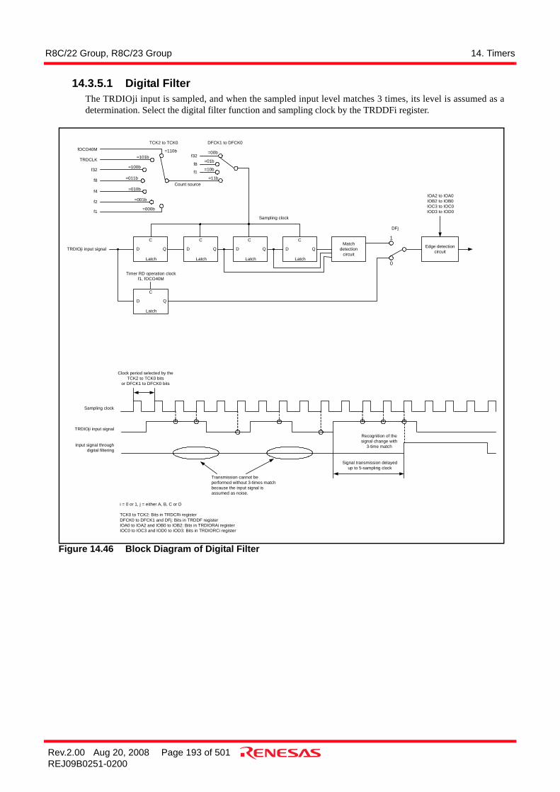
R8C/22 Group, R8C/23 Group 14. Timers
Rev.2.00 Aug 20, 2008 Page 193 of 501REJ09B0251-0200
14.3.5.1 Digital FilterThe TRDIOji input is sampled, and when the sampled input level matches 3 times, its level is assumed as adetermination. Select the digital filter function and sampling clock by the TRDDFi register.
Figure 14.46 Block Diagram of Digital Filter
C
D Q
Latch
C
D Q
Latch
C
D Q
Latch
Matchdetection
circuit
Edge detectioncircuit
DFj
Sampling clock
IOA2 to IOA0IOB2 to IOB0IOC3 to IOC0IOD3 to IOD0
DFCK1 to DFCK0
TRDIOji input signal
Clock period selected by theTCK2 to TCK0 bits
or DFCK1 to DFCK0 bits
Sampling clock
TRDIOji input signal
Input signal throughdigital filtering
Transmission cannot beperformed without 3-times matchbecause the input signal isassumed as noise.
Signal transmission delayedup to 5-sampling clock
Recognition of thesignal change with
3-time match
f32
f8
f1
i = 0 or 1, j = either A, B, C or D
TCK0 to TCK2: Bits in TRDCRi registerDFCK0 to DFCK1 and DFj: Bits in TRDDF registerIOA0 to IOA2 and IOB0 to IOB2: Bits in TRDIORAi registerIOC0 to IOC3 and IOD0 to IOD3: Bits in TRDIORCi register
C
D Q
Latch
C
D Q
Latch
Timer RD operation clockf1, fOCO40M
Count source
=101b
=100b
=011b
=110b
=010b
=001b
fOCO40M
f4
f2
f8
f32
TRDCLK
f1 =000b
=00b
=01b
=10b
=11b
TCK2 to TCK0
1
0

R8C/22 Group, R8C/23 Group 14. Timers
Rev.2.00 Aug 20, 2008 Page 194 of 501REJ09B0251-0200
14.3.6 Output Compare FunctionThis function is to detect the match (compare match) of the content in the TRDGRji (j = either A, B, C and D)register with the content in the TRDi (i = 0 or 1) register. When the content matches, any level is output fromthe TRDIOji pin. Since this function is enabled with a combination of the TRDIOji pin and TRDGRji register,any of the output compare function, other modes or functions can be selected every pin.Figure 14.47 shows the Block Diagram of Output Compare Function, Table 14.25 lists the Output CompareFunction Specifications. Figures 14.48 to 14.59 list the Registers Associated with Output Compare Functionand Figure 14.60 shows the Operating Example of Output Compare Function.
Figure 14.47 Block Diagram of Output Compare Function
TRDIOA0 Outputcontrol
Comparator TRDGRA0
TRD0
TRDIOC0 Outputcontrol
Comparator TRDGRC0
Compare match signal
TRDIOB0 Outputcontrol
Comparator TRDGRB0
TRDIOD0 Outputcontrol
Comparator TRDGRD0
Channel 0
TRDIOA1 Outputcontrol
Comparator TRDGRA1
TRD1
TRDIOC1 Outputcontrol
Comparator TRDGRC1
TRDIOB1 Outputcontrol
Comparator TRDGRB1
TRDIOD1 Outputcontrol
Comparator TRDGRD1
Channel 1
Compare match signal
Compare match signal
Compare match signal
Compare match signal
Compare match signal
Compare match signal
Compare match signal
IOC3 = 0 inTRDIORC0 register
IOC3 = 1
IOD3 = 0 inTRDIORD0 register
IOD3 = 1
IOC3 = 0 inTRDIORC1 register
IOC3 = 1
IOD3 = 0 inTRDIORD1 register
IOD3 = 1

R8C/22 Group, R8C/23 Group 14. Timers
Rev.2.00 Aug 20, 2008 Page 195 of 501REJ09B0251-0200
i = 0 or 1, j = either A, B, C or D
Table 14.25 Output Compare Function SpecificationsItem Specification
Count Sources f1, f2, f4, f8, f32, fOCO40MExternal signal input to the TRDCLK pin (valid edge selected by a program)
Count Operations IncrementCount Period • When the CCLR2 to CCLR0 bits in the TRDCRi register are set to 000b (free-
running operation)1/fk × 65536 fk: Frequency of count source
• The CCLR1 to CCLR0 bits in the TRDCRi register are set to 01b or 10b (set the TRDi register to 0000h at the compare match in the TRDGRji register.)Frequency of count source x (n + 1)n: Setting value in the TRDGRji register
Waveform Output Timing Compare matchCount Start Condition Write 1 (count starts) to the TSTARTi bit in the TRDSTR register.Count Stop Conditions • Write 0 (count stops) to the TSTARTi bit in the TRDSTR register when the CSELi
bit in the TRDSTR register is set to 1.The output compare output pin holds output level before the count stops.
• When the CSELi bit in the TRDSTR register is set to 0, the count stops at the compare match in the TRDGRAi register.The output compare output pin holds level after output change by the compare match.
Interrupt Request Generation Timing
• Compare match (the content in the TRDi register matches with the content in the TRDGRji register.)
• TRDi register overflowsTRDIOA0 Pin Function Programmable I/O port, output-compare output or TRDCLK (external clock) inputTRDIOB0, TRDIOC0, TRDIOD0, TRDIOA1 to TRDIOD1 Pin Functions
Programmable I/O port or output-compare output (select every pin)
INT0 Pin Function Programmable I/O port, pulse output forced cutoff signal input or INT0 interrupt input
Read from Timer The count value can be read by reading the TRDi register.Write to Timer • When the SYNC bit in the TRDMR register is set to 0 (channels 0 and 1 operate
independently)Data can be written to the TRDi register.
• When the SYNC bit in the TRDMR register is set to 1 (channels 0 and 1 operate synchronously).Data can be written to both the TRD0 and TRD1 registers by writing to the TRDi register.
Selection Functions • Output-compare output pin selectedEither 1 pin or multiple pins of the TRDIOAi, TRDIOBi, TRDIOCi or TRDIODi pin.
• Output level at the compare match selected“L” output, “H” output or output level inversed
• Initial output level selectedSet the level at period from the count start to the compare match.
• Timing to set the TRDi register to 0000hOverflow or compare match in the TRDGRAi register
• Buffer operation (refer to 14.3.2 Buffer Operation)• Synchronous operation (refer to 14.3.3 Synchronous Operation)• Output pin in the TRDGRCi and TRDGRDi registers changed
The TRDGRCi register can be used as output control of the TRDIOAi pin and the TRDGRDi register can be used as output control of the TRDIOBi pin.
• Pulse output forced cutoff signal input (refer to 14.3.4 Pulse Output Forced Cutoff)
• Timer RD can be used as the internal timer without output.

R8C/22 Group, R8C/23 Group 14. Timers
Rev.2.00 Aug 20, 2008 Page 196 of 501REJ09B0251-0200
Figure 14.48 Registers TRDSTR and TRDMR in Output Compare Function
Timer RD Start Register(1)
Symbol Address After ResetTRDSTR 0137h 11111100b
Bit Symbol Bit Name Function RW
NOTES:1.
2.3.4.5.
Set the TRDSTR register using the MOV instruction (do not use the bit handling instruction). Refer to 14.3.12.1TRDSTR Register of Notes on Timer RD.
TRD0 count operation selectbit
0 : Count stops at the compare match w ith the TRDGRA0 register after the count clear1 : Count continues at the compare match w ith the TRDGRA0 register after the count clear
CSEL0 RW
RW
TRD1 count operation selectbit
0 : Count stops at the compare match w ith the TRDGRA1 register after the count clear1 : Count continues at the compare match w ith the TRDGRA1 register after the count clear
——
(b7 - b4)
RW
TSTART1 RWTRD1 count start f lag(5) 0 : Count stops(3)
1 : Count starts
TRD0 count start f lag(4) 0 : Count stops(2)
1 : Count starts
Nothing is assigned. If necessary, set to 0.When read, the content is 1.
b7 b6 b5 b4 b3 b2
CSEL1
b1 b0
TSTART0
When the CSEL0 bit is set to 1, w rite 0 to the TSTART0 bit.When the CSEL1 bit is set to 1, w rite 0 to the TSTART1 bit.When the CSEL0 bit is set to 0 and generating the compare match signal (TRDIOA0), this bit is set to 0 (count stops).When the CSEL1 bit is set to 0 and generating the compare match signal (TRDIOA1), this bit is set to 0 (count stops).
Timer RD Mode Register
Symbol Address After ResetTRDMR 0138h 00001110b
Bit Symbol Bit Name Function RW
NOTE:1. When selecting 0 (change the TRDGRji register output pin) by the IOj3 (j = C or D) bit in the TRDIORCi (i = 0 or 1)
register, set the BFji bit in the TRDMR register to 0.
RWBFC1
BFD1TRDGRD1 register functionselection bit(1)
0 : General register1 : Buffer register of TRDGRB1 register RW
TRDGRC0 register functionselection bit(1)
0 : General register1 : Buffer register of TRDGRA0 registerBFC0 RW
RWTRDGRD0 register functionselection bit(1)
0 : General register1 : Buffer register of TRDGRB0 register
TRDGRC1 register functionselection bit(1)
0 : General register1 : Buffer register of TRDGRA1 register
RW
—(b3 - b1) —
Timer RD synchronous bit 0 : TRD0 and TRD1 registers operate independently1 : TRD0 and TRD1 registers operate synchronously
Nothing is assigned. If necessary, set to 0.When read, the content is 1.
b7 b6 b5 b4 b3 b2
BFD0
b1 b0
SYNC

R8C/22 Group, R8C/23 Group 14. Timers
Rev.2.00 Aug 20, 2008 Page 197 of 501REJ09B0251-0200
Figure 14.49 TRDPMR Register in Output Compare Function
Timer RD PWM Mode Register
Symbol Address After ResetTRDPMR 0139h 10001000b
Bit Symbol Bit Name Function RW
b3 b2
—(b3)
b1 b0
0 00
PWMB0
b7 b6 b5 b4
0 0 0
RW
PWMC0 RW
PWM mode of TRDIOB0 selection bit Set to 0 (timer mode) in the outputcompare function
PWM mode of TRDIOC0 selection bit Set to 0 (timer mode) in the outputcompare function
—
PWM mode of TRDIOB1 selection bit Set to 0 (timer mode) in the outputcompare function
RW
RW
Nothing is assigned. If necessary, set to 0.When read, the content is 1.
Set to 0 (timer mode) in the outputcompare function
PWM mode of TRDIOD0 selection bit Set to 0 (timer mode) in the outputcompare functionPWMD0 RW
—(b7) —
PWMB1
PWMC1 RW
Nothing is assigned. If necessary, set to 0.When read, the content is 1.
PWM mode of TRDIOC1 selection bit Set to 0 (timer mode) in the outputcompare function
PWMD1PWM mode of TRDIOD1 selection bit

R8C/22 Group, R8C/23 Group 14. Timers
Rev.2.00 Aug 20, 2008 Page 198 of 501REJ09B0251-0200
Figure 14.50 TRDFCR Register in Output Compare Function
Timer RD Function Control Register
Symbol Address After ResetTRDFCR 013Ah 10000000b
Bit Symbol Bit Name Function RW
NOTES:1.2. When bits CMD1 to CMD0 are set to 00b (timer mode, PWM mode, or PWM3 mode), the setting of the PWM3 bit is
enabled.
b3 b2
OLS1
b1 b0
0 01b7 b6 b5 b4
RW
CMD1 RW
Combination mode selection bit(1) Set to 00b (timer mode, PWM mode, orPWM3 mode) in the output comparefunction.
CMD0
Normal-phase output level selectionbit (in reset synchronous PWM modeor complementary PWM mode)
This bit is disabled in the output comparefunction.
Set bits CMD1 to CMD0 w hen both the TSTART0 and TSTART1 bits in the TRDSTR register are set to 0 (count stops).
OLS0 RW
RWCounter-phase output level selectionbit (in reset synchronous PWM modeor complementary PWM mode)
This bit is disabled in the output comparefunction.
A/D trigger enable bit(in complementary PWM mode)
This bit is disabled in the output comparefunction. RW
PWM3 RW
ADTRG
ADEGA/D trigger edge selection bit(in complementary PWM mode)
This bit is disabled in the output comparefunction. RW
PWM3 mode selection bit(2) Set this bit to 1 (other than PWM3 mode) inthe output compare function.
STCLKExternal clock input selection bit 0 : External clock input disabled
1 : External clock input enabled RW

R8C/22 Group, R8C/23 Group 14. Timers
Rev.2.00 Aug 20, 2008 Page 199 of 501REJ09B0251-0200
Figure 14.51 Registers TRDOER1 to TRDOER2 in Output Compare Function
Timer RD Output Master Enable Register 1
Symbol Address After ResetTRDOER1 013Bh FFhBit Symbol Bit Name Function RW
b3 b2
ED0
b1 b0
EA0
b7 b6 b5 b4
RW
EB0 RW
TRDIOA0 output disable bit 0 : Enable output1 : Disable output (The TRDIOA0 pin is used as a programmable I/O port.)
TRDIOB0 output disable bit 0 : Enable output1 : Disable output (The TRDIOB0 pin is used as a programmable I/O port.)
TRDIOC0 output disable bit 0 : Enable output1 : Disable output (The TRDIOC0 pin is used as a programmable I/O port.)
EC0 RW
RW
TRDIOA1 output disable bit 0 : Enable output1 : Disable output (The TRDIOA1 pin is used as a programmable I/O port.)
RW
RW
TRDIOD0 output disable bit 0 : Enable output1 : Disable output (The TRDIOD0 pin is used as a programmable I/O port.)
TRDIOC1 output disable bit 0 : Enable output1 : Disable output (The TRDIOC1 pin is used as a programmable I/O port.)
EC1 RW
EA1
EB1 RW
TRDIOD1 output disable bit 0 : Enable output1 : Disable output (The TRDIOD1 pin is used as a programmable I/O port.)
TRDIOB1 output disable bit 0 : Enable output1 : Disable output (The TRDIOB1 pin is used as a programmable I/O port.)
EC1
Timer RD Output Master Enable Register 2
Symbol Address After ResetTRDOER2 013Ch 01111111bBit Symbol Bit Name Function RW
INT0_____
of pulse output forced 0 : Pulse output forced cutoff input disabledcutoff signal input enabled 1 : Pulse output forced cutoff input enabledbit(1) (All bits in the TRDOER1 register
are set to 1 (disable output) w hen “L” is applied to the INT0
_____ pin)
NOTE:1.
b3 b2 b1 b0b7 b6 b5 b4
Refer to 14.3.4 Pulse Output Forced Cutoff.
——
(b6 - b0)Nothing is assigned. If necessary, set to 0.When read, the content is 1.
RWPTO

R8C/22 Group, R8C/23 Group 14. Timers
Rev.2.00 Aug 20, 2008 Page 200 of 501REJ09B0251-0200
Figure 14.52 TRDOCR Register in Output Compare Function
Timer RD Output Control Register(1,2)
Symbol Address After ResetTRDOCR 013Dh 00h
Bit Symbol Bit Name Function RW
NOTES:1.
2.
TOA1
TOB1 RW
TRDIOD1 initial output level selectionbit
0 : “L”1 : “H”
TRDIOB1 initial output level selectionbit
TOC1TRDIOC1 initial output level selectionbit
TRDIOC0 initial output level selectionbit
Write to the TRDOCR register w hen both the TSTART0 and TSTART1 bits in the TRDSTR register are set to 0 (countstops).
TOC0 RW
RW
TRDIOA1 initial output level selectionbit
RW
RW
TRDIOD0 initial output level selectionbit
TOD1 RW
RW
TOB0 RW
TRDIOA0 output level selection bit 0 : Initial output “L”1 : Initial output “H”
TRDIOB0 output level selection bit 0 : Initial output “L”1 : Initial output “H”
TOA0
b7 b6 b5 b4
When the pin functions are w aveform output (refer to Table 14.12 to 14.19) and the TRDOCR register is set, theinitial output level is output.
b3 b2
TOD0
b1 b0

R8C/22 Group, R8C/23 Group 14. Timers
Rev.2.00 Aug 20, 2008 Page 201 of 501REJ09B0251-0200
Figure 14.53 Registers TRDCR0 to TRDCR1 in Output Compare Function
Timer RD Control Register i (i = 0 or 1)
Symbol Address After ResetTRDCR0TRDCR1
0140h0150h
00h00h
Bit Symbol Bit Name Function RW
NOTES: 1.2.
3.
RW
TCK1 RW
TCK0
RW
RW
RW
CCLR2
CCLR1 RW
Count source selection bit b2 b1 b0
0 0 0 : f10 0 1 : f20 1 0 : f40 1 1 : f81 0 0 : f321 0 1 : TRDCLK input(1)
1 1 0 : fOCO40M1 1 1 : Do not set
External clock edgeselection bit(2)
b4 b3
0 0 : Count at the rising edge0 1 : Count at the falling edge1 0 : Count at both edges1 1 : Do not set
b7 b6 b5 b4 b3 b2
CKEG0
b1 b0
TCK2
This bit is enabled w hen the SYNC bit in the TRDMR register is set to 1 (TRD0 and TRD1 operate synchronously).
This bit is enabled w hen the TCK2 to TCK0 bits are set to 101b (TRDCLK input) and the STCLK bit in the TRDFCRregister is set to 1 (external clock input enabled).
RW
CKEG1
CCLR0 RW
b7 b6 b5
0 0 0 : Disable clear (free-running operation)0 0 1 : Clear by the compare match in the TRDGRAi register0 1 0 : Clear by the compare match in the TRDGRBi register0 1 1 : Synchronous clear (clear simultaneously w ith other channel counter)(3)
1 0 0 : Do not set1 0 1 : Clear by the compare match in the TRDGRCi register1 1 0 : Clear by the compare match in the TRDGRDi register1 1 1 : Do not set
TRDi counter clear selectionbit
This bit is enabled w hen the STCLK bit in the TRDFCR register is set to 1 (external clock input enabled).

R8C/22 Group, R8C/23 Group 14. Timers
Rev.2.00 Aug 20, 2008 Page 202 of 501REJ09B0251-0200
Figure 14.54 Registers TRDIORA0 to TRDIORA1 in Output Compare Function
Timer RD I/O Control Register Ai (i = 0 or 1)
Symbol Address After ResetTRDIORA0TRDIORA1
0141h0151h
10001000b10001000b
Bit Symbol Bit Name Function RW
NOTES: 1.
2.
TRDGRA mode selectionbit(1)
Set to 0 (output compare) in the output comparefunction RW
Input capture input sw itchbit
Set to 1RW
RW
RW
IOA1
IOA0
TRDGRA control bit b1 b0
0 0 : Disable pin output by the compare match (TRDIOAi pin functions as programmable I/O port)0 1 : “L” output by the compare match in the TRDGRAi register1 0 : “H” output by the compare match in the TRDGRAi register1 1 : Toggle output by the compare match in the TRDGRAi register
—(b7)
IOB2 RW
TRDGRB control bit b5 b4
0 0 : Disable pin output by the compare match (TRDIOBi pin functions as programmable I/O port)0 1 : “L” output by the compare match in the TRDGRBi register1 0 : “H” output by the compare match in the TRDGRBi1 1 : Toggle output by the compare match in the TRDGRBi register
Nothing is assigned. If necessary, set to 0.When read, the content is 1.
b7 b6 b5 b4
0b3 b2
IOA3
b1 b0
1 0
IOA2
When selecting 1 (The TRDGRDi register is used as a buffer register of TRDGRBi register) for this bit by the BFDi bitin the TRDMR register, set the IOD2 bit in the TRDIORCi register to the same as the IOB2 bit in the TRDIORAi register.
—
IOB0
IOB1 RW
When selecting 1 (The TRDGRCi register is used as a buffer register of the TRDGRAi register) for this bit by the BFCibit in the TRDMR register, set the IOC2 bit in the TRDIORCi register to the same as the IOA2 bit in the TRDIORAiregister.
TRDGRB mode selectionbit(2)
Set to 0 (output compare) in the output comparefunction
RW

R8C/22 Group, R8C/23 Group 14. Timers
Rev.2.00 Aug 20, 2008 Page 203 of 501REJ09B0251-0200
Figure 14.55 Registers TRDIORC0 to TRDIORC1 in Output Compare Function
Timer RD I/O Control Register Ci (i = 0 or 1)
Symbol Address After ResetTRDIORC0TRDIORC1
0142h0152h
10001000b10001000b
Bit Symbol Bit Name Function RW
NOTES: 1.
2. When selecting 1 (The TRDGRDi register is used as a buffer register of TRDGRBi register) for this bit by the BFDi bitin the TRDMR register, set the IOD2 bit in the TRDIORCi register to the same as the IOB2 bit in the TRDIORAi register.
TRDGRC mode selectionbit(1)
Set to 0 (output compare) in the output comparefunction RW
TRDGRC register functionselection bit(1)
0 : TRDIOA output register (Refer to 14.3.6.1 Changing Output Pins in Registers TRDGRCi (i = 0 or 1) and TRDGRDi)1 : General register or buffer register
RW
IOD0
IOD1
RW
RW
RW
IOC1
IOC0
TRDGRC control bit b1 b0
0 0 : Disable pin output by the compare match0 1 : “L” output by the compare match in the TRDGRCi register1 0 : “H” output by the compare match in the TRDGRCi register1 1 : Toggle output by the compare match in the TRDGRCi register
RW
TRDGRD control bit b5 b4
0 0 : Disable pin output by the compare match0 1 : “L” output by the compare match in the TRDGRDi register1 0 : “H” output by the compare match in the TRDGRDi register1 1 : Toggle output by the compare match in the TRDGRDi register
b7 b6 b5 b4
0b3 b2
IOC3
b1 b0
0
IOC2
When selecting 1 (The TRDGRCi register is used as a buffer register of the TRDGRAi register) for this bit by the BFCibit in the TRDMR register, set the IOC2 bit in the TRDIORCi register to the same as the IOA2 bit in the TRDIORAiregister.
TRDGRD mode selectionbit(2)
Set to 0 (output compare) in the output comparefunction
IOD3
IOD2 RW
TRDGRD register functionselection bit
0 : TRDIOB output register (Refer to 14.3.6.1 Changing Output Pins in Registers TRDGRCi (i = 0 or 1) and TRDGRDi)1 : General register or buffer register
RW

R8C/22 Group, R8C/23 Group 14. Timers
Rev.2.00 Aug 20, 2008 Page 204 of 501REJ09B0251-0200
Figure 14.56 Registers TRDSR0 to TRDSR1 in Output Compare Function
Timer RD Status Register i (i = 0 or 1)
Symbol Address After ResetTRDSR0TRDSR1
0143h0153h
11100000b11000000b
Bit Symbol Bit Name Function RW
NOTES:1.2.
3. Including w hen the BFji bit (j = C or D) in the TRDMR register is set to 1 (TRDGRji is used as the buffer register).
The w riting results are as follow s:• This bit is set to 0 w hen the read result is 1 and w riting 0 to the same bit.• This bit remains unchanged even if the read result is 0 and w riting 0 to the same bit. (This bit remains 1 even if this bit is set to 1 from 0 after reading, and w riting 0.)• This bit remains unchanged w hen w riting 1.
b3 b2
IMFD
b1 b0b7 b6 b5 b4
RW
IMFB RW
Input capture/compare matchflag A
[Source for setting this bit to 0]Write 0 after read.(2)
[Source for setting this bit to 1]When the value in the TRDi register matches w iththe value in the TRDGRAi register.
Input capture/compare matchflag B
[Source for setting this bit to 0]Write 0 after read.(2)
[Source for setting this bit to 1]When the value in the TRDi register matches w iththe value in the TRDGRBi register.
IMFA
Input capture/compare matchflag C
[Source for setting this bit to 0]Write 0 after read.(2)
[Source for setting this bit to 1]When the value in the TRDi register matches w iththe value in the TRDGRCi register.(3)
Nothing is assigned to the b5 in the TRDSR0 register. When w riting to the b5, w rite 0. When reading, its content is 1.
IMFC RW
RW
Input capture/compare matchflag D
[Source for setting this bit to 0]Write 0 after read.(2)
[Source for setting this bit to 1]When the value in the TRDi register matches w iththe value in the TRDGRDi register.(3)
Overflow f lag [Source for setting this bit to 0]Write 0 after read.(2)
[Source for setting this bit to 1]When the TRDi register overf low s.
—(b7 - b6) —
Nothing is assigned. If necessary, set to 0.When read, the content is 1.
RWOVF
UDFUnderflow f lag(1) This bit is disabled in the output compare function.
RW
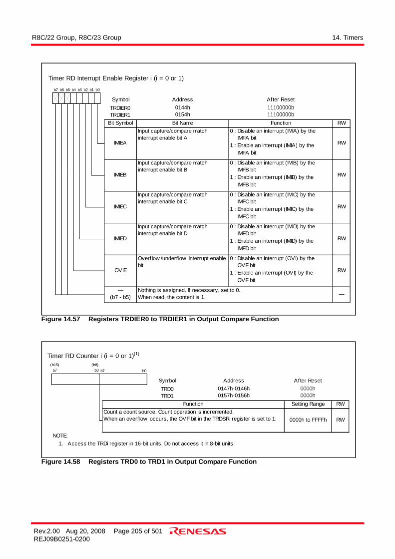
R8C/22 Group, R8C/23 Group 14. Timers
Rev.2.00 Aug 20, 2008 Page 205 of 501REJ09B0251-0200
Figure 14.57 Registers TRDIER0 to TRDIER1 in Output Compare Function
Figure 14.58 Registers TRD0 to TRD1 in Output Compare Function
Timer RD Interrupt Enable Register i (i = 0 or 1)
Symbol Address After ResetTRDIER0TRDIER1
0144h0154h
11100000b11100000b
Bit Symbol Bit Name Function RW
RWOVIE
—(b7 - b5) —
Nothing is assigned. If necessary, set to 0.When read, the content is 1.
Input capture/compare matchinterrupt enable bit C
0 : Disable an interrupt (IMIC) by the IMFC bit1 : Enable an interrupt (IMIC) by the IMFC bit
IMIEC RW
RW
Input capture/compare matchinterrupt enable bit D
0 : Disable an interrupt (IMID) by the IMFD bit1 : Enable an interrupt (IMID) by the IMFD bit
Overflow /underflow interrupt enablebit
0 : Disable an interrupt (OVI) by the OVF bit1 : Enable an interrupt (OVI) by the OVF bit
RW
IMIEB RW
Input capture/compare matchinterrupt enable bit A
0 : Disable an interrupt (IMIA) by the IMFA bit1 : Enable an interrupt (IMIA) by the IMFA bit
Input capture/compare matchinterrupt enable bit B
0 : Disable an interrupt (IMIB) by the IMFB bit1 : Enable an interrupt (IMIB) by the IMFB bit
IMIEA
b7 b6 b5 b4 b3 b2
IMIED
b1 b0
Timer RD Counter i (i = 0 or 1)(1)
Symbol Address After ResetTRD0TRD1
0147h-0146h0157h-0156h
0000h0000h
Setting Range RW
NOTE:1.
FunctionCount a count source. Count operation is incremented.When an overflow occurs, the OVF bit in the TRDSRi register is set to 1. 0000h to FFFFh RW
Access the TRDi register in 16-bit units. Do not access it in 8-bit units.
b0b7(b8)
b0(b15)
b7

R8C/22 Group, R8C/23 Group 14. Timers
Rev.2.00 Aug 20, 2008 Page 206 of 501REJ09B0251-0200
Figure 14.59 Registers TRDGRAi, TRDGRBi, TRDGRCi and TRDGRDi in Output Compare Function
The following registers are disabled in the output compare function:TRDDF0, TRDDF1, TRDPOCR0 and TRDPOCR1
i = 0 or 1, j = either A, B, C or DBFji: Bit in TRDMR register IOj3: Bit in TRDIORCi register
Table 14.26 TRDGRji Register Functions in Output Compare Function
RegisterSetting
Register Function Output-Compare Output PinBFji IOj3
TRDGRAi − − General register. Write the compare value. TRDIOAiTRDGRBi TRDIOBiTRDGRCi 0 1 General register. Write the compare value. TRDIOCiTRDGRDi TRDIODiTRDGRCi 1 1 Buffer register. Write the next compare value
(refer to 14.3.2 Buffer Operation.)TRDIOAi
TRDGRDi TRDIOBiTRDGRCi 0 0 TRDIOAi output control (refer to 14.3.6.1 Changing
Output Pins in Registers TRDGRCi (i = 0 or 1) and TRDGRDi.)
TRDIOAiTRDGRDi TRDIOBi
Timer RD General Register Ai, Bi, Ci and Di (i = 0 or 1)(1)
Symbol Address After Reset
TRDGRA0TRDGRB0TRDGRC0TRDGRD0TRDGRA1TRDGRB1TRDGRC1TRDGRD1
0149h-0148h014Bh-014Ah014Dh-014Ch014Fh-014Eh0159h-0158h015Bh-015Ah015Dh-015Ch015Fh-015Eh
FFFFhFFFFhFFFFhFFFFhFFFFhFFFFhFFFFhFFFFh
RW
NOTE:1.
RW
FunctionRefer to Table 14.26 TRDGRji Register Functions in Output Compare Function
Access the TRDGRAi to TRDGRDi registers in 16-bit units. Do not access them in 8-bit units.
b0b7(b8)
b0(b15)
b7

R8C/22 Group, R8C/23 Group 14. Timers
Rev.2.00 Aug 20, 2008 Page 207 of 501REJ09B0251-0200
Figure 14.60 Operating Example of Output Compare Function
m
n
p
Value in TRDi register
m + 1 m + 1
TSTARTi bit inTRDSTR register
1
0
TRDIOAi output
IMFA bit inTRDSRi register
1
0
n + 1
TRDIOBi output
IMFB bit inTRDSRi register
1
0
TRDIOCi output
IMFC bit inTRDSRi register
1
0
Initial output “H”
“L” output by compare match
Set to “0” by a program
Count source
i = 0 or 1 m: Setting value in TRDGRAi registern: Setting value in TRDGRBi registerp: Setting value in TRDGRCi register
The above applies to the following conditions:The CSELi bit in the TRDSTR register is set to 1. (The TRDi register is not stopped by the compare match.)The BFCi and BFDi bits in the TRDMR register are set to 0. (The TRDGRCi and TRDGRDi registers are not used as the buffer register.)The EAi, EBi and ECi bits in the TRDOER1 register are set to 0. (Enable the TRDIOAi, TRDIOBi and TRDIOCi pin outputs.)The CCLR2 to CCLR0 bits in the TRDCRi register are set to 001b. (Set the TRDi register to 000h by the compare match in the TRDGRAi register.)The TOAi and TOBi bits in the TRDOCR register is set to 0. (initial output “L” to the compare match), the TOCi bit is set to 1. (initial output “H” to the compare match.)The IOA2 to IOA0 bits in the TRDIORAi register are set to 011b. (TRDIOAi output inversed at the TRDGRAi register compare match.)The IOB2 to IOB0 bits in the TRDIORAi register are set to 010b. (TRDIOBi “H” output at the TRDGRBi register compare match.)The IOC3 to IOC0 bits in the TRDIORCi register are set to 1001b. (TRDIOCi “L” output at the TRDGRCi register compare match.)The IOD3 bit in the TRDIORCi register is set to 1. (TRDGRDi register does not control TRDIOBi pin output.)
m
n
p
n + 1
P + 1
Countstop
Countrestarts
Output levelheld
Output levelheld
Output levelheld
Set to 0 by a program
Set to 0 by a program
“H” output by compare match
Output inversed by compare match
Initial output “L”
Initial output “L”

R8C/22 Group, R8C/23 Group 14. Timers
Rev.2.00 Aug 20, 2008 Page 208 of 501REJ09B0251-0200
14.3.6.1 Changing Output Pins in Registers TRDGRCi (i = 0 or 1) and TRDGRDiThe TRDGRCi register can be used as output control of the TRDIOAi pin and the TRDGRDi register can beused as output control of the TRDIOBi pin. Therefore, each pin output can be controlled as follows:
• TRDIOAi output is controlled by the values in the TRDGRAi and TRDGRCi registers.• TRDIOBi output is controlled by the values in the TRDGRBi and TRDGRDi registers.
Figure 14.61 Changing Output Pins in Registers TRDGRCi and TRDGRDi
Change output pins in the TRDGRCi and TRDGRDi registers as below:• Select 0 (change TRDGRji register output pin) by the IOj3 (j = C or D) bit in the TRDIORCi register.• Set the BFji bit in the TRDMR register to 0 (general register).• Set the different value in the TRDGRCi register and the TRDGRAi register. Also, set the different value in
the TRDGRDi register and the TRDGRBi register.
TRDIOA0 Outputcontrol
Comparator TRDGRA0
TRD0
TRDIOC0 Outputcontrol
Comparator TRDGRC0
Compare match signal
TRDIOB0 Outputcontrol
Comparator TRDGRB0
TRDIOD0 Outputcontrol
Comparator TRDGRD0
Channel 0
TRDIOA1 OutputControl
Comparator TRDGRA1
TRD1
TRDIOC1 OutputControl
Comparator TRDGRC1
TRDIOB1 OutputControl
Comparator TRDGRB1
TRDIOD1 OutputControl
Comparator TRDGRD1
Channel 1
Compare match signal
Compare match signal
Compare match signal
Compare match signal
Compare match signal
Compare match signal
Compare match signal
IOC3 = 0 inTRDIORC0 register
IOC3 = 1
IOD3 = 0 inTRDIORD0 register
IOD3 = 1
IOC3 = 0 inTRDIORC1 register
IOC3 = 1
IOD3 = 0 inTRDIORD1 register
IOD3 = 1

R8C/22 Group, R8C/23 Group 14. Timers
Rev.2.00 Aug 20, 2008 Page 209 of 501REJ09B0251-0200
Figure 14.62 lists the Operating Example When TRDGRCi Register is Used for Output Control of TRDIOAiPin and TRDGRDi Register is Used for Output Control of TRDIOBi Pin.
Figure 14.62 Operating Example When TRDGRCi Register is Used for Output Control of TRDIOAi Pin and TRDGRDi Register is Used for Output Control of TRDIOBi Pin
Set to 0 by a programSet to 0 by a program
Value in TRDi register
Count source
TRDIOAi output
FFFFh
TRDIOBi output
m: Setting Value in TRDGRAi registern: Setting Value in TRDGRCi registerp: Setting Value in TRDGRBi registerq: Setting Value in TRDGRDi register
The above applies to the following conditions:The CSELi bit in the TRDSTR register is set to 1. (The TRDi register is not stopped by the compare match.)The BFCi and BFDi bits in the TRDMR register are set to 0. (The TRDGRCi and TRDGRDi registers are not used as the buffer register.)The EAi and EBi bits in the TRDOER1 register are set to 0. (Enable TRDIOAi and TRDIOBi pin outputs.)The CCLR2 to CCLR0 bits in the TRDCRi register are set to 001b. (Set the TRDi register to 0000h by the compare match in the TRDGRAi register.)The TOAi and TOBi bits in the TRDOCR register are set to 0. (initial output “L” to the compare match.)The IOA2 to IOA0 bits in the TRDIORAi register are set to 011b. (TRDIOAi output inversed at the TRDGRAi register compare match.)The IOB2 to IOB0 bits in the TRDIORAi register are set to 011b. (TRDIOBi output inversed at the TRDGRBi register compare match.)The IOC3 to IOC0 bits in the TRDIORCi register are set to 0011b. (TRDIOAi output inversed at the TRDGRCi register compare match.)The IOD3 to IOD0 bits in the TRDIORCi register are set to 0011b. (TRDIOBi output inversed at the TRDGRDi register compare match.)
i = 0 or 1
m
n
p
m + 1
n + 1
q
0000h
m - n
p + 1
p - qq + 1
IMFA bit inTRDSRi register
1
0
IMFC bit inTRDSRi register
1
0
Set to 0 by a program
Output inversed by compare match
Initial output “L”
IMFB bit inTRDSRi register
1
0
IMFD bit inTRDSRi register
1
0
Initial output “L”
Set to 0 by a program
Output inversed by compare match

R8C/22 Group, R8C/23 Group 14. Timers
Rev.2.00 Aug 20, 2008 Page 210 of 501REJ09B0251-0200
14.3.7 PWM ModePWM mode is to output a PWM waveform. Up to 3 PWM waveforms with the same period can be output by 1channel. Also, Up to 6 PWM waveforms with the same period can be output by synchronizing Channels 0 and1. Since this mode functions by a combination of the TRDIOji (i = 0 or 1, j = B, C or D) pin and TRDGRjiregister, any of PWM mode, other modes or functions can be selected every pin. (However, since theTRDGRAi register is used when using any pin for PWM mode, the TRDGRAi register cannot be used for othermodes.)Figure 14.63 shows the Block Diagram of PWM Mode, Table 14.27 lists the PWM Mode Specifications.Figures 14.64 to 14.73 show the Registers Associated with PWM Mode and Figures 14.74 to 14.75 show theOperations of PWM Mode.
Figure 14.63 Block Diagram of PWM Mode
TRDIOBi
Outputcontrol
TRDGRAi
TRDi
Compare match signal
TRDGRBiTRDIOCi
TRDGRCi
TRDGRDi
TRDIODi
(Note 1)
(Note 2)
i = 0 or 1
NOTES:1. When the BFCi bit in the TRDMR register is set to 1 (the TRDGRCi register is used as the
buffer register of the TRDGRAi register).2. When the BFDi bit in the TRDMR register is set to 1 (the TRDGRDi register is used as the
buffer register of the TRDGRBi register).
Compare match signal
Compare match signal
Compare match signal
Comparator
Comparator
Comparator
Comparator

R8C/22 Group, R8C/23 Group 14. Timers
Rev.2.00 Aug 20, 2008 Page 211 of 501REJ09B0251-0200
i = 0 or 1, j = either B, C or D, h = either A, B, C or D
Table 14.27 PWM Mode SpecificationsItem Specification
Count Sources f1, f2, f4, f8, f32, fOCO40MExternal signal input to the TRDCLK pin (valid edge selected by a program)
Count Operations IncrementPWM Waveform PWM period: 1/fk x (m+1)
Active level width: 1/fk x (m-n)Inactive level width: 1/fk x (n+1) fk: Frequency of count source m: Setting value in the TRDGRAi register n: Setting value in the TRDGRji register
Count Start Condition Write 1 (count starts) to the TSTARTi bit in the TRDSTR register.Count Stop Conditions • Write 0 (count stops) to the TSTARTi bit in the TRDSTR register
when the CSELi bit in the TRDSTR register is set to 1.The PWM output pin holds output level before the count stops.
• When the CSELi bit in the TRDSTR register is set to 0, the count stops at the compare match in the TRDGRAi register.The PWM output pin holds level after output change by the compare match.
Interrupt Request Generation Timing
• Compare match (the content in the TRDi register matches with the content in the TRDGRhi register.)
• TRDi register overflowsTRDIOA0 Pin Function Programmable I/O port or TRDCLK (external clock) inputTRDIOA1 Pin Function Programmable I/O portTRDIOB0, TRDIOC0, TRDIOD0, TRDIOB1, TRDIOC1, TRDIOD1 Pin Functions
Programmable I/O port or pulse output (select every pin)
INT0 Pin Function Programmable I/O port, pulse output forced cutoff signal input or INT0 interrupt input
Read from Timer The count value can be read by reading the TRDi register.Write to Timer The value can be written to the TRDi register.Selection Functions • 1 to 3 PWM output pins selected per 1 channel
Either 1 pin or multiple pins of the TRDIOBi, TRDIOCi or TRDIODi pin.
• The active level selected every pin.• Initial output level selected every pin.• Synchronous operation (refer to 14.3.3 Synchronous Operation.)• Buffer operation (refer to 14.3.2 Buffer Operation.)• Pulse output forced cutoff signal input (refer to 14.3.4 Pulse Output
Forced Cutoff.)
m + 1
n + 1 m - n (When “L” is selected for the active level)

R8C/22 Group, R8C/23 Group 14. Timers
Rev.2.00 Aug 20, 2008 Page 212 of 501REJ09B0251-0200
Figure 14.64 TRDSTR Register in PWM Mode
Timer RD Start Register(1)
Symbol Address After ResetTRDSTR 0137h 11111100b
Bit Symbol Bit Name Function RW
NOTES:1.
2.3.4.5.
When the CSEL0 bit is set to 1, w rite 0 to the TSTART0 bit.When the CSEL1 bit is set to 1, w rite 0 to the TSTART1 bit.When the CSEL0 bit is set to 0 and generating the compare match signal (TRDIOA0), this bit is set to 0 (count stops).When the CSEL1 bit is set to 0 and generating the compare match signal (TRDIOA1), this bit is set to 0 (count stops).
b3 b2
CSEL1
b1 b0
TSTART0
b7 b6 b5 b4
Nothing is assigned. When w rite, set to 0.When read, its content is 1.
RW
TSTART1 RWTRD1 count start f lag(5) 0 : Count stops(3)
1 : Count starts
TRD0 count start f lag(4) 0 : Count stops(2)
1 : Count starts
Set the TRDSTR register using the MOV instruction (do not use the bit handling instruction). Refer to 14.3.12.1TRDSTR Register of Notes on Timer RD.
TRD0 count operation select bit 0 : Count stops at the compare match w ith the TRDGRA0 register1 : Count continues at the compare match w ith the TRDGRA0 register
CSEL0 RW
RW
TRD1 count operation select bit 0 : Count stops at the compare match w ith the TRDGRA1 register1 : Count continues at the compare match w ith the TRDGRA1 register
——
(b7 - b4)

R8C/22 Group, R8C/23 Group 14. Timers
Rev.2.00 Aug 20, 2008 Page 213 of 501REJ09B0251-0200
Figure 14.65 Registers TRDMR and TRDPMR in PWM Mode
Timer RD Mode Register
Symbol Address After ResetTRDMR 0138h 00001110b
Bit Symbol Bit Name Function RW
RW
BFC1
BFD1TRDGRD1 register functionselection bit
0 : General register1 : Buffer register of TRDGRB1 register
RWTRDGRD0 register functionselection bit
0 : General register1 : Buffer register of TRDGRB0 register
TRDGRC1 register functionselection bit
0 : General register1 : Buffer register of TRDGRA1 register RW
TRDGRC0 register functionselection bit
0 : General register1 : Buffer register of TRDGRA0 registerBFC0 RW
RW
—(b3 - b1) —
Timer RD synchronous bit 0 : TRD0 and TRD1 registers operate independently1 : TRD0 and TRD1 registers operate synchronously
Nothing is assigned. If necessary, set to 0.When read, the content is 1.
b7 b6 b5 b4 b3 b2
BFD0
b1 b0
SYNC
Timer RD PWM Mode Register
Symbol Address After ResetTRDPMR 0139h 10001000b
Bit Symbol Bit Name Function RW
Nothing is assigned. If necessary, set to 0.When read, the content is 1.
PWM mode of TRDIOC1 selection bit 0 : Timer mode1 : PWM mode
PWMD1PWM mode of TRDIOD1 selection bit 0 : Timer mode
1 : PWM mode—
(b7) —
PWMB1
PWMC1 RW
Nothing is assigned. If necessary, set to 0.When read, the content is 1.
PWM mode of TRDIOD0 selection bit 0 : Timer mode1 : PWM modePWMD0 RW
—
PWM mode of TRDIOB1 selection bit 0 : Timer mode1 : PWM mode
RW
RW
RW
PWMC0 RW
PWM mode of TRDIOB0 selection bit 0 : Timer mode1 : PWM mode
PWM mode of TRDIOC0 selection bit 0 : Timer mode1 : PWM mode
b7 b6 b5 b4 b3 b2
—(b3)
b1 b0
PWMB0

R8C/22 Group, R8C/23 Group 14. Timers
Rev.2.00 Aug 20, 2008 Page 214 of 501REJ09B0251-0200
Figure 14.66 TRDFCR Register in PWM Mode
Timer RD Function Control Register
Symbol Address After ResetTRDFCR 013Ah 10000000b
Bit Symbol Bit Name Function RW
NOTES:1.2. When bits CMD1 to CMD0 are set to 00b (timer mode, PWM mode, or PWM3 mode), the setting of the PWM3 bit is
enabled.
b3 b2
OLS1
b1 b0
0 01b7 b6 b5 b4
RW
CMD1 RW
Combination mode selection bit(1) Set to 00b (timer mode, PWM mode, orPWM3 mode) in PWM mode.CMD0
Normal-phase output level selectionbit (in reset synchronous PWM modeor complementary PWM mode)
This bit is disabled in PWM mode.
Set bits CMD1 to CMD0 w hen both the TSTART0 and TSTART1 bits in the TRDSTR register are set to 0 (count stops).
OLS0 RW
RWCounter-phase output level selectionbit (in reset synchronous PWM modeor complementary PWM mode)
This bit is disabled in PWM mode.
A/D trigger enable bit(in complementary PWM mode)
This bit is disabled in PWM mode.RW
PWM3 RW
ADTRG
ADEGA/D trigger edge selection bit(in complementary PWM mode)
This bit is disabled in PWM mode.RW
PWM3 mode selection bit(2) Set this bit to 1 (other than PWM3 mode) inPWM mode.
STCLKExternal clock input selection bit 0 : External clock input disabled
1 : External clock input enabled RW

R8C/22 Group, R8C/23 Group 14. Timers
Rev.2.00 Aug 20, 2008 Page 215 of 501REJ09B0251-0200
Figure 14.67 Registers TRDOER1 to TRDOER2 in PWM Mode
Timer RD Output Master Enable Register 1
Symbol Address After ResetTRDOER1 013Bh FFhBit Symbol Bit Name Function RW
b3 b2
ED0
b1 b0
1
EA0
b7 b6 b5 b4
1
RW
EB0 RW
TRDIOA0 output disable bit Set this bit to 1 (The TRDIOA0 pin isused as a programmable I/O mode) inPWM mode.
TRDIOB0 output disable bit 0 : Enable output1 : Disable output (The TRDIOB0 pin is used as a programmable I/O mode.)
RW
TRDIOA1 output disable bit Set this bit to 1 (The TRDIOA0 pin isused as a programmable I/O mode) inPWM mode.
RW
RW
TRDIOD0 output disable bit 0 : Enable output1 : Disable output (The TRDIOD0 pin is used as a programmable I/O mode.)
TRDIOC1 output disable bit 0 : Enable output1 : Disable output (The TRDIOC1 pin is used as a programmable I/O mode.)
TRDIOC0 output disable bit 0 : Enable output1 : Disable output (The TRDIOC0 pin is used as a programmable I/O mode.)
EC0 RW
ED1 RW
EA1
EB1 RW
TRDIOD1 output disable bit 0 : Enable output1 : Disable output (The TRDIOD1 pin is used as a programmable I/O mode.)
TRDIOB1 output disable bit 0 : Enable output1 : Disable output (The TRDIOB1 pin is used as a programmable I/O mode.)
EC1
Timer RD Output Master Enable Register 2
Symbol Address After ResetTRDOER2 013Ch 01111111bBit Symbol Bit Name Function RW
INT0_____
of pulse output forced 0 : Pulse output forced cutoff input disabled1 : Pulse output forced cutoff input enabled (All bits in the TRDOER1 register are set to 1 (disable output) w hen “L” is applied to the INT0
_____ pin)
NOTE: 1.
b3 b2 b1 b0b7 b6 b5 b4
Refer to 14.3.4 Pulse Output Forced Cutoff.
——
(b6 - b0)Nothing is assigned. When w rite, set to 0.When read, its content is 1.
RWPTO
cutoff signal input enabled bit(1)

R8C/22 Group, R8C/23 Group 14. Timers
Rev.2.00 Aug 20, 2008 Page 216 of 501REJ09B0251-0200
Figure 14.68 Registers TRDOCR and TRDCR0 to TRDCR1 in PWM Mode
Timer RD Output Control Register(1)
Symbol Address After ResetTRDOCR 013Dh 00h
Bit Symbol Bit Name Function RW
NOTES:1.
2. When the pin functions are w aveform output (refer to Table 14.13 to 14.15; Table 14.17 to 14.19) and the TRDOCRregister is set, the initial output level is output.
b3 b2
TOD0
b1 b0
0
TOA0
b7 b6 b5 b4
0
TRDIOD0 initial output level selection bit(2)
TOD1 RW
RW
TOB0 RW
TRDIOA0 output level selection bit Set this bit to 0 (enableoutput) in PWM mode
TRDIOB0 output level selection bit(2)
TRDIOC0 initial output level selection bit(2)
0 : Initial output is inactive level1 : Initial output is active level
Set this bit to 0 (enableoutput) in PWM mode
Write to the TRDOCR register w hen both the TSTART0 and TSTART1 bits in the TRDSTR register are set to 0 (countstops).
TOC0 RWRW
TRDIOA1 initial output level selection bit
RW
RW
0 : Inactive level1 : Active level
TOA1
TOB1 RW
TRDIOD1 initial output level selection bit(2)
TRDIOB1 initial output level selection bit(2)
TOC1 TRDIOC1 initial output level selection bit(2)
Timer RD Control Register i (i = 0 or 1)
Symbol Address After ResetTRDCR0TRDCR1
0140h0150h
00h00h
Bit Symbol Bit Name Function RW
NOTES: 1.2. This bit is enabled w hen the TCK2 to TCK0 bits are set to 101b (TRDCLK input) and the STCLK bit in the TRDFCR
register is set to 1 (external clock input enabled).
RW
CKEG1
CCLR0 RWSet to 001b (the TRDi register clear at thecompare match w ith TRDGRAi register) in PWMmode.
TRDi counter clear selection bit
This bit is enabled w hen the STCLK bit in the TRDFCR register is set to 1 (external clock input enabled).
b3 b2
CKEG0
b1 b0
TCK2
0 0 1b7 b6 b5 b4
RW
RW
RW
CCLR2CCLR1 RW
Count source selection bit b2 b1 b0
0 0 0 : f10 0 1 : f20 1 0 : f40 1 1 : f81 0 0 : f321 0 1 : TRDCLK input(1)
1 1 0 : fOCO40M1 1 1 : Do not set
External clock edge selectionbit(2)
b4 b3
0 0 : Count at the rising edge0 1 : Count at the falling edge1 0 : Count at both edges1 1 : Do not set
RW
TCK1 RW
TCK0

R8C/22 Group, R8C/23 Group 14. Timers
Rev.2.00 Aug 20, 2008 Page 217 of 501REJ09B0251-0200
Figure 14.69 Registers TRDSR0 to TRDSR1 in PWM Mode
Timer RD Status Register i (i = 0 or 1)
Symbol Address After ResetTRDSR0TRDSR1
0143h0153h
11100000b11000000b
Bit Symbol Bit Name Function RW
NOTES:1.
2.
3.
—(b7 - b6) —
Nothing is assigned. If necessary, set to 0.When read, the content is 1.
RWOVF
UDFUnderflow f lag(1) This bit is disabled in PWM mode.
RW
Input capture/compare matchflag C
[Source for setting this bit to 0]Write 0 after read.(2)
[Source for setting this bit to 1]When the value in the TRDi register matches w iththe value in the TRDGRCi register.(3)
Nothing is assigned to the bit 5 in the TRDSR0 register. When w riting to the bit 5, w rite 0. When reading, its content is1.
IMFC RW
RW
Input capture/compare matchflag D
[Source for setting this bit to 0]Write 0 after read.(2)
[Source for setting this bit to 1]When the value in the TRDi register matches w iththe value in the TRDGRDi register.(3)
Overflow f lag [Source for setting this bit to 0]Write 0 after read.(2)
[Source for setting this bit to 1]When the TRDi register overf low s.
RW
IMFB RW
Input capture/compare matchflag A
[Source for setting this bit to 0]Write 0 after read.(2)
[Source for setting this bit to 1]When the value in the TRDi register matches w iththe value in the TRDGRAi register.
Input capture/compare matchflag B
[Source for setting this bit to 0]Write 0 after read.(2)
[Source for setting this bit to 1]When the value in the TRDi register matches w iththe value in the TRDGRBi register.
IMFA
b7 b6 b5 b4
Including w hen the BFji bit (j = C or D) in the TRDMR register is set to 1 (TRDGRji is used as the buffer register).
The w riting results are as follow s:• This bit is set to 0 w hen the read result is 1 and w riting 0 to the same bit.• This bit remains unchanged even if the read result is 0 and w riting 0 to the same bit. (This bit remains 1 even if this bit is set to 1 from 0 after reading, and w riting 0.)• This bit remains unchanged w hen w riting 1.
b3 b2
IMFD
b1 b0

R8C/22 Group, R8C/23 Group 14. Timers
Rev.2.00 Aug 20, 2008 Page 218 of 501REJ09B0251-0200
Figure 14.70 Registers TRDIER0 to TRDIER1 in PWM Mode
Timer RD Interrupt Enable Register i (i = 0 or 1)
Symbol Address After ResetTRDIER0TRDIER1
0144h0154h
11100000b11100000b
Bit Symbol Bit Name Function RW
RWOVIE
—(b7 - b5) —
Nothing is assigned. If necessary, set to 0.When read, the content is 1.
Input capture/compare matchinterrupt enable bit C
0 : Disable an interrupt (IMIC) by the IMFC bit1 : Enable an interrupt (IMIC) by the IMFC bit
IMIEC RW
RW
Input capture/compare matchinterrupt enable bit D
0 : Disable an interrupt (IMID) by the IMFD bit1 : Enable an interrupt (IMID) by the IMFD bit
Overflow /underflow interrupt enablebit
0 : Disable an interrupt (OVI) by the OVF bit1 : Enable an interrupt (OVI) by the OVF bit
RW
IMIEB RW
Input capture/compare matchinterrupt enable bit A
0 : Disable an interrupt (IMIA) by the IMFA bit1 : Enable an interrupt (IMIA) by the IMFA bit
Input capture/compare matchinterrupt enable bit B
0 : Disable an interrupt (IMIB) by the IMFB bit1 : Enable an interrupt (IMIB) by the IMFB bit
IMIEA
b7 b6 b5 b4 b3 b2
IMIED
b1 b0

R8C/22 Group, R8C/23 Group 14. Timers
Rev.2.00 Aug 20, 2008 Page 219 of 501REJ09B0251-0200
Figure 14.71 Registers TRDPOCR0 to TRDPOCR1 in PWM Mode
Figure 14.72 Registers TRD0 to TRD1 in PWM Mode
Timer RD PWM Mode Output Level Control Register i (i = 0 or 1)
Symbol Address After ResetTRDPOCR0TRDPOCR1
0145h0155h
11111000b11111000b
Bit Symbol Bit Name Function RW
b3 b2
—(b7 - b3)
b1 b0
POLD
b7 b6 b5 b4
RW
POLC RW
PWM mode output level control bitB
0 : “L” active of TRDIOBi output level is selected1 : “H” active of TRDIOBi output level is selected
PWM mode output level control bitC
0 : “L” active of TRDIOCi output level is selected1 : “H” active of TRDIOCi output level is selected
POLB
—Nothing is assigned. If necessary, set to 0.When read, the content is 1.
PWM mode output level control bitD
0 : “L” active of TRDIODi output level is selected1 : “H” active of TRDIODi output level is selected
RW
Timer RD Counter i (i = 0 or 1)(1)
Symbol Address After ResetTRD0TRD1
0147h-0146h0157h-0156h
0000h0000h
Setting Range RW
NOTE:1.
FunctionCount a count source. Count operation is incremented.When an overflow occurs, the OVF bit in the TRDSRi register is set to 1. 0000h to FFFFh RW
Access the TRDi register in 16-bit units. Do not access it in 8-bit units.
b0b7(b8)
b0(b15)
b7

R8C/22 Group, R8C/23 Group 14. Timers
Rev.2.00 Aug 20, 2008 Page 220 of 501REJ09B0251-0200
Figure 14.73 Registers TRDGRAi, TRDGRBi, TRDGRCi and TRDGRDi in PWM Mode
The following registers are disabled in the PWM mode:TRDDF0, TRDDF1, TRDIORA0, TRDIORC0, TRDIORA1 and TRDIORC1
i = 0 or 1BFCi, BFDi: Bits in TRDMR register
Table 14.28 TRDGRji Register Functions in PWM ModeRegister Setting Register Function PWM Output Pin
TRDGRAi − General register. Set the PWM period. −TRDGRBi − General register. Set the changing point of PWM output TRDIOBiTRDGRCi BFCi = 0 General register. Set the changing point of PWM output TRDIOCiTRDGRDi BFDi = 0 TRDIODiTRDGRCi BFCi = 1 Buffer register. Set the next PWM period
(refer to 14.3.2 Buffer Operation.)−
TRDGRDi BFDi = 1 Buffer register. Set the changing point of the next PWM output(refer to 14.3.2 Buffer Operation.)
TRDIOBi
Timer RD General Register Ai, Bi, Ci and Di (i = 0 or 1)(1)
Symbol Address After Reset
TRDGRA0TRDGRB0TRDGRC0TRDGRD0TRDGRA1TRDGRB1TRDGRC1TRDGRD1
0149h-0148h014Bh-014Ah014Dh-014Ch014Fh-014Eh0159h-0158h015Bh-015Ah015Dh-015Ch015Fh-015Eh
FFFFhFFFFhFFFFhFFFFhFFFFhFFFFhFFFFhFFFFh
RW
NOTE:1.
(b8)b0
(b15)b7 b0b7
RW
FunctionRefer to Table 14.28 TRDGRji Register Functions in PWM Mode
Access the TRDGRAi to TRDGRDi registers in 16-bit units. Do not access them in 8-bit units.

R8C/22 Group, R8C/23 Group 14. Timers
Rev.2.00 Aug 20, 2008 Page 221 of 501REJ09B0251-0200
Figure 14.74 Operating Example of PWM Mode
m
n
p
Value in TRDi register
Count source
m + 1
n + 1
TRDIOCi output
q
m - n
p + 1 m - p
m - qq + 1
TRDIODi output
m: Setting value in TRDGRAi registern: Setting value in TRDGRBi registerp: Setting value in TRDGRCi registerq: Setting value in TRDGRDi register
Inactive Level “L”Active level “H”
Inactive Level “H”
Active level “L”
Initial output “L” tocompare match
Initial output “H” tocompare match
Set to 0 by a program Set to 0 by a program
Set to 0 by a program
TRDIOBi output
IMFA bit inTRDSRi register
1
0
IMFB bit inTRDSRi register
1
0
IMFC bit inTRDSRi register
1
0
IMFD bit inTRDSRi register
1
0
i = 0 or 1
Set to 0 by a program
The above applies to the following conditions:The BFCi and BFDi bits in the TRDMR register are set to 0. (The TRDGRCi and TRDGRDi registers are not used as the buffer register.)The EBi, ECi and EDi bits in the TRDOER1 register are set to 0. (Enable TRDIOBi, TRDIOCi and TRDIODi pin outputs.)The TOBi and TOCi bits in the TRDOCR register are set to 0 (inactive level), the TODi bit is set to 1. (active level)The POLB bit in the TRDPOCRi register is set to 1 (active level “H”), the POLC and POLD bits are set to 0. (active level “L”)
Initial output “L” tocompare match

R8C/22 Group, R8C/23 Group 14. Timers
Rev.2.00 Aug 20, 2008 Page 222 of 501REJ09B0251-0200
Figure 14.75 Operating Example of PWM Mode (Duty 0%, Duty 100%)
m
p
q
Value in TRDi register
n
m: Setting value in TRDGRAi register
Set to 0 by a program
Rewrite by a program
0000h
q
Duty 0 %
TRDGRBi register
IMFA bit inTRDSRi register
1
0
IMFB bit inTRDSRi register
1
0
TSTARTi bit inTRDSTR register
TRDIOBi output
p (p > m)n
Since the compare match in the TRDGRBi register isnot generated, “L” is not applied to TRDIOBi output
1
0
m
p
Value in TRDi register
n
0000h
TRDGRBi register
IMFA bit inTRDSRi register
1
0
IMFB bit inTRDSRi register
1
0
TSTARTi bit inTRDSTR register
TRDIOBi output
pn
1
0
“L” is applied to TRDIOBi output by the comparematch in the TRDGRBi register with no change.
m
i = 0 or 1
The above applies to the following conditions:The EBi bit in the TRDOER1 register is set to 0. (Enable TRDIOBi output.)The POLB bit in the TRDPOCRi register is set to 0. (active level “L”)
Rewrite by a program
Set to 0 by a program
Set to 0 by a program
When the compare matches in the TRDGRAi and TRDGRBi registers are generatedsimultaneously, the compare match in the TRDGRBi register has a priority.“L” is applied to TRDIOBi output without any change.
Duty 100 %
Set to 0 by a program

R8C/22 Group, R8C/23 Group 14. Timers
Rev.2.00 Aug 20, 2008 Page 223 of 501REJ09B0251-0200
14.3.8 Reset Synchronous PWM ModeOutput 3 normal-phases and 3 counter-phases of the PWM waveform with the same period (no three-phase,sawtooth wave modulation and dead time).Figure 14.76 shows the Block Diagram of Reset Synchronous PWM Mode, Table 14.29 lists the ResetSynchronous PWM Mode Specifications. Figures 14.77 to 14.84 show the Registers Associated with ResetSynchronous PWM Mode and Figure 14.85 shows the Operating Example of Reset Synchronous PWM Mode.Refer to Figure 14.75 Operating Example of PWM Mode (Duty 0%, Duty 100%) for the operation examplein PWM Mode of duty 0% and duty 100%.
Figure 14.76 Block Diagram of Reset Synchronous PWM Mode
Period TRDIOC0
TRDIOB0
TRDIOD0
TRDIOA1
TRDIOC1
TRDIOB1
TRDIOD1
PWM1
PWM2
PWM3
Waveform control
TRDGRB0register
TRDGRA1register
TRDGRB1register
Normal-phase
Counter-phase
TRDGRA0register
TRDGRD0register
TRDGRC1register
TRDGRD1register
TRDGRC0register
Buffer(1)
Normal-phase
Counter-phase
Normal-phase
Counter-phase
NOTE:1. When the BFC0, BFD0, BFC1 and BFD1 bits in the TRDMR register are set to 1 (buffer register).

R8C/22 Group, R8C/23 Group 14. Timers
Rev.2.00 Aug 20, 2008 Page 224 of 501REJ09B0251-0200
j = either A, B, C or D
Table 14.29 Reset Synchronous PWM Mode SpecificationsItem Specification
Count Sources f1, f2, f4, f8, f32, fOCO40MExternal signal input to the TRDCLK pin (valid edge selected by a program)
Count Operations The TRD0 register is incremented (The TRD1 register is not used.)PWM Waveform PWM period: 1/fk × (m + 1)
Active level width of normal-phase: 1/fk × (m - n)Active level width of counter-phase:1/fk × (n + 1) fk: Frequency of count source m: Setting value in the TRDGRA0 register n: Setting value in the TRDGRB0 register (PWM output 1),
Setting value in the TRDGRA1 register (PWM output 2),Setting value in the TRDGRB1 register (PWM output 3)
Count Start Condition Write 1 (count starts) to the TSTART0 bit in the TRDSTR register.Count Stop Conditions • Write 0 (count stops) to the TSTART0 bit in the TRDSTR register
when the CSEL0 bit in the TRDSTR register is set to 1.The PWM output pin holds output level before the count stops
• When the CSEL0 bit in the TRDSTR register is set to 0, the count stops at the compare match in the TRDGRA0 register.The PWM output pin holds level after output change by the compare match.
Interrupt Request Generation Timing
• Compare match (the content in the TRD0 register matches with the content in the TRDGRj0, TRDGRA1 and TRDGRB1 registers.)
• The TRD0 register overflows TRDIOA0 Pin Function Programmable I/O port or TRDCLK (external clock) inputTRDIOB0 Pin Function PWM output 1 normal-phase outputTRDIOD0 Pin Function PWM output 1 counter-phase outputTRDIOA1 Pin Function PWM output 2 normal-phase outputTRDIOC1 Pin Function PWM output 2 counter-phase outputTRDIOB1 Pin Function PWM output 3 normal-phase outputTRDIOD1 Pin Function PWM output 3 counter-phase outputTRDIOC0 Pin Function Output inverted every period of PWMINT0 Pin Function Programmable I/O port, pulse output forced cutoff signal input or INT0
interrupt inputRead from Timer The count value can be read by reading the TRD0 register.Write to Timer The value can be written to the TRD0 register.Selection Functions • The active level of normal-phase and counter-phase and initial
output level selected individually.• Buffer operation (refer to 14.3.2 Buffer Operation.)• Pulse output forced cutoff signal input (refer to 14.3.4 Pulse Output
Forced Cutoff.)
m + 1
Normal-phase
n + 1 (When “L” is selected for the active level)
Counter-phase
m - n

R8C/22 Group, R8C/23 Group 14. Timers
Rev.2.00 Aug 20, 2008 Page 225 of 501REJ09B0251-0200
Figure 14.77 TRDSTR Register in Reset Synchronous PWM Mode
Timer RD Start Register(1)
Symbol Address After ResetTRDSTR 0137h 11111100b
Bit Symbol Bit Name Function RW
NOTES:1.
2.3.4.5.
—(b7 - b4)
Nothing is assigned. If necessary, set to 0.When read, the content is 1.
Set the TRDSTR register using the MOV instruction (do not use the bit handling instruction). Refer to 14.3.12.1TRDSTR Register of Notes on Timer RD.
RW
TRD1 count operation select bit 0 : Count stops at the compare match w ith the TRDGRA1 register1 : Count continues at the compare match w ith the TRDGRA1 register
—
TRD0 count operation select bit 0 : Count stops at the compare match w ith the TRDGRA0 register1 : Count continues at the compare match w ith the TRDGRA0 register
CSEL0 RW
RW
TSTART1 RWTRD1 count start f lag(5)
[This bit is not used in reset synchronous PWM mode]
0 : Count stops(3)
1 : Count starts
TRD0 count start f lag(4) 0 : Count stops(2)
1 : Count starts
b7 b6 b5 b4 b3 b2
CSEL1
b1 b0
TSTART0
When the CSEL0 bit is set to 1, w rite 0 to the TSTART0 bit.When the CSEL1 bit is set to 1, w rite 0 to the TSTART1 bit.When the CSEL0 bit is set to 0 and generating the compare match signal(TRDIOA0), this bit is set to 0 (count stops).When the CSEL1 bit is set to 0 and generating the compare match signal(TRDIOA1), this bit is set to 0 (count stops).

R8C/22 Group, R8C/23 Group 14. Timers
Rev.2.00 Aug 20, 2008 Page 226 of 501REJ09B0251-0200
Figure 14.78 Registers TRDMR and TRDFCR in Reset Synchronous PWM Mode
Timer RD Mode Register
Symbol Address After ResetTRDMR 0138h 00001110b
Bit Symbol Bit Name Function RW
b3 b2
BFD0
b1 b0
0
SYNC
b7 b6 b5 b4
RW
—(b3 - b1) —
Timer RD synchronous bit Set this bit to 0 (the TRD0 and TRD1 registersoperate independently.) in reset synchronousPWM mode.
Nothing is assigned. If necessary, set to 0.When read, the content is 1.
RWTRDGRD0 register functionselection bit
0 : General register1 : Buffer register of TRDGRB0 register
TRDGRC1 register functionselection bit
0 : General register1 : Buffer register of TRDGRA1 register RW
TRDGRC0 register functionselection bit
0 : General register1 : Buffer register of TRDGRA0 registerBFC0 RW
RW
BFC1
BFD1TRDGRD1 register functionselection bit
0 : General register1 : Buffer register of TRDGRB1 register
Timer RD Function Control Register
Symbol Address After ResetTRDFCR 013Ah 10000000b
Bit Symbol Bit Name Function RW
NOTES:1.
2.3. When bits CMD1 to CMD0 are set to 00b (timer mode, PWM mode, or PWM3 mode), the setting of the PWM3 bit is
enabled.
b3 b2
OLS1
b1 b0
0 1b7 b6 b5 b4
RWCMD1 RW
Combination mode selection bit(1,2) Set to 01b (reset synchronous PWMmode) in reset synchronous PWM mode.
CMD0
Normal-phase output level selectionbit (in reset synchronous PWM modeor complementary PWM mode)
0 : Initial output “H” Active level “L”1 : Initial output “L” Active level “H”
Set bits CMD1 to CMD0 w hen both the TSTART0 and TSTART1 bits in the TRDSTR register are set to 0 (count stops).
OLS0 RW
RW
Counter-phase output level selectionbit (in reset synchronous PWM modeor complementary PWM mode)
0 : Initial output “H” Active level “L”1 : Initial output “L” Active level “H”
A/D trigger enable bit(in complementary PWM mode)
This bit is disabled in reset synchronousPWM mode. RW
PWM3 RW
ADTRG
ADEGA/D trigger edge selection bit(in complementary PWM mode)
This bit is disabled in reset synchronousPWM mode. RW
PWM3 mode selection bit(3) This bit is disabled in reset synchronousPWM mode.
When bits CMD1 to CMD0 are set to 01b, 10b, or 11b, the MCU enters reset synchronous PWM mode orcomplementary PWM mode in spite of the setting of the TRDPMR register.
STCLKExternal clock input selection bit 0 : External clock input disabled
1 : External clock input enabled RW

R8C/22 Group, R8C/23 Group 14. Timers
Rev.2.00 Aug 20, 2008 Page 227 of 501REJ09B0251-0200
Figure 14.79 Registers TRDOER1 to TRDOER2 in Reset Synchronous PWM Mode
Timer RD Output Master Enable Register 1
Symbol Address After ResetTRDOER1 013Bh FFhBit Symbol Bit Name Function RW
ED1 RW
EA1
EB1 RW
TRDIOD1 output disable bit 0 : Enable output1 : Disable output (the TRDIOD1 pin is used as a programmable I/O port.)
TRDIOB1 output disable bit 0 : Enable output1 : Disable output (the TRDIOB1 pin is used as a programmable I/O port.)
EC1
RW
TRDIOA1 output disable bit 0 : Enable output1 : Disable output (the TRDIOA1 pin is used as a programmable I/O port.)
RW
RW
TRDIOD0 output disable bit 0 : Enable output1 : Disable output (the TRDIOD0 pin is used as a programmable I/O port.)
TRDIOC1 output disable bit 0 : Enable output1 : Disable output (the TRDIOC1 pin is used as a programmable I/O port.)
TRDIOC0 output disable bit 0 : Enable output1 : Disable output (the TRDIOC0 pin is used as a programmable I/O port.)
EC0 RW
RW
EB0 RW
TRDIOA0 output disable bit Set this bit to 1 (the TRDIOA0 pin isused as a programmable I/O port) in resetsynchronous PWM mode.
TRDIOB0 output disable bit 0 : Enable output1 : Disable output (the TRDIOB0 pin is used as a programmable I/O port.)
b7 b6 b5 b4 b3 b2
ED0
b1 b0
1
EA0
Timer RD Output Master Enable Register 2
Symbol Address After ResetTRDOER2 013Ch 01111111bBit Symbol Bit Name Function RW
INT0_____
of pulse output forced 0 : Pulse output forced cutoff input disabled1 : Pulse output forced cutoff input enabled (all bits in the TRDOER1 register are set to 1 (disable output) w hen “L” is applied to the INT0
_____ pin)
NOTE:1.
b3 b2 b1 b0b7 b6 b5 b4
Refer to 14.3.4 Pulse Output Forced Cutoff.
——
(b6 - b0)Nothing is assigned. If necessary, set to 0.When read, the content is 1.
RWPTO
cutoff signal input enabled bit(1)

R8C/22 Group, R8C/23 Group 14. Timers
Rev.2.00 Aug 20, 2008 Page 228 of 501REJ09B0251-0200
Figure 14.80 TRDCR0 Register in Reset Synchronous PWM Mode
Timer RD Control Register 0(3)
Symbol Address After ResetTRDCR0 0140h 00h
Bit Symbol Bit Name Function RW
NOTES: 1.2.
3.
RW
TCK1 RW
TCK0
RW
RW
RW
CCLR2CCLR1 RW
Count source selection bit b2 b1b0
0 0 0 : f10 0 1 : f20 1 0 : f40 1 1 : f81 0 0 : f321 0 1 : TRDCLK input(1)
1 1 0 : fOCO40M1 1 1 : Do not set
External clock edge selectionbit(2)
b4 b3
0 0 : Count at the rising edge0 1 : Count at the falling edge1 0 : Count at both edges1 1 : Do not set
b7 b6 b5 b4
0 0 1b3 b2
CKEG0
b1 b0
TCK2
The TRDCR1 register is not used in reset synchronous PWM mode.
This bit is enabled w hen the TCK2 to TCK0 bits are set to “101b” (TRDCLK input) and the STCLK bit in the TRDFCRregister is set to 1 (external clock input enabled).
RW
CKEG1
CCLR0 RWSet to 001b (TRD0 register clear at thecompare match w ith TRDGRA0 register) inreset synchronous PWM mode.
TRD0 counter clear selection bit
This bit is enabled w hen the STCLK bit in the TRDFCR register is set to 1 (external clock input enabled).

R8C/22 Group, R8C/23 Group 14. Timers
Rev.2.00 Aug 20, 2008 Page 229 of 501REJ09B0251-0200
Figure 14.81 Registers TRDSR0 to TRDSR1 in Reset Synchronous PWM Mode
Timer RD Status Register i (i = 0 or 1)
Symbol Address After ResetTRDSR0TRDSR1
0143h0153h
11100000b11000000b
Bit Symbol Bit Name Function RW
NOTES:1.2.
3.
—(b7 - b6) —
Nothing is assigned. If necessary, set to 0.When read, the content is 1.
RWOVF
UDFUnderflow f lag(1) This bit is disabled in reset synchronous PWM
mode. RW
Input capture/compare matchflag C
[Source for setting this bit to 0]Write 0 after read.(2)
[Source for setting this bit to 1]When the value in the TRDi register matches w iththe value in the TRDGRCi register.(3)
Nothing is assigned to the b5 in the TRDSR0 register. When w riting to the b5, w rite 0. When reading, its content is 1.
IMFC RW
RW
Input capture/compare matchflag D
[Source for setting this bit to 0]Write 0 after read.(2)
[Source for setting this bit to 1]When the value in the TRDi register matches w iththe value in the TRDGRDi register.(3)
Overflow f lag [Source for setting this bit to 0]Write 0 after read.(2)
[Source for setting this bit to 1]When the TRDi register overf low s.
RW
IMFB RW
Input capture/compare matchflag A
[Source for setting this bit to 0]Write 0 after read.(2)
[Source for setting this bit to 1]When the value in the TRDi register matchesw ith the value in the TRDGRAi register.
Input capture/compare matchflag B
[Source for setting this bit to 0]Write 0 after read.(2)
[Source for setting this bit to 1]When the value in the TRDi register matchesw ith the value in the TRDGRBi register.
IMFA
b7 b6 b5 b4
Including w hen the BFji bit in the TRDMR register is set to 1 (TRDGRji is used as the buffer register).
The w riting results are as follow s:• This bit is set to 0 w hen the read result is 1 and w riting 0 to the same bit.• This bit remains unchanged even if the read result is 0 and w riting 0 to the same bit. (This bit remains 1 even if this bit is set to 1 from 0 after reading, and w riting 0.)• This bit remains unchanged w hen w riting 1.
b3 b2
IMFD
b1 b0

R8C/22 Group, R8C/23 Group 14. Timers
Rev.2.00 Aug 20, 2008 Page 230 of 501REJ09B0251-0200
Figure 14.82 Registers TRDIER0 to TRDIER1 in Reset Synchronous PWM Mode
Figure 14.83 TRD0 Registrar in Reset Synchronous PWM Mode
Timer RD Interrupt Enable Register i (i = 0 or 1)
Symbol Address After ResetTRDIER0TRDIER1
0144h0154h
11100000b11100000b
Bit Symbol Bit Name Function RW
b3 b2
IMIED
b1 b0b7 b6 b5 b4
RW
IMIEB RW
Input capture/compare matchinterrupt enable bit A
0 : Disable an interrupt (IMIA) by the IMFA bit1 : Enable an interrupt (IMIA) by the IMFA bit
Input capture/compare matchinterrupt enable bit B
0 : Disable an interrupt (IMIB) by the IMFB bit1 : Enable an interrupt (IMIB) by the IMFB bit
IMIEA
Input capture/compare matchinterrupt enable bit C
0 : Disable an interrupt (IMIC) by the IMFC bit1 : Enable an interrupt (IMIC) by the IMFC bit
IMIEC RW
RW
Input capture/compare matchinterrupt enable bit D
0 : Disable an interrupt (IMID) by the IMFD bit1 : Enable an interrupt (IMID) by the IMFD bit
Overflow /underflow interrupt enablebit
0 : Disable an interrupt (OVI) by the OVF bit1 : Enable an interrupt (OVI) by the OVF bit
RWOVIE
—(b7 - b5) —
Nothing is assigned. If necessary, set to 0.When read, the content is 1.
Timer RD Counter 0(1,2)
Symbol Address After ResetTRD0 0147h-0146h 0000h
Setting Range RW
NOTES:1.2.
(b8)b0
(b15)b7 b0b7
The TRD1 register is not used in reset synchronous PWM mode.
FunctionCount a count source. Count operation is incremented.When an overflow occurs, the OVF bit in the TRDSR0 register is set to 1. 0000h to FFFFh RW
Access the TRD0 register in 16-bit units. Do not access it in 8-bit units.

R8C/22 Group, R8C/23 Group 14. Timers
Rev.2.00 Aug 20, 2008 Page 231 of 501REJ09B0251-0200
Figure 14.84 Registers TRDGRAi, TRDGRBi, TRDGRCi and TRDGRDi in Reset Synchronous PWM Mode
The following registers are disabled in the reset synchronous PWM mode:TRDPMR, TRDOCR, TRDDF0, TRDDF1, TRDIORA0, TRDIORC0, TRDPOCR0, TRDIORA1, TRDIORC1and TRDPOCR1
BFC0, BFD0, BFC1, BFD1: Bits in TRDMR Register
Table 14.30 TRDGRji Register Functions in Reset Synchronous PWM ModeRegister Setting Register Function PWM Output Pin
TRDGRA0 − General register. Set the PWM period. (Output inverted every period of TRDIOC0 and PWM pins)
TRDGRB0 − General register. Set the changing point of PWM1 output.
TRDIOB0TRDIOD0
TRDGRC0 BFC0 = 0 (These registers are not used in reset synchronous PWM mode.)
−TRDGRD0 BFD0 = 0TRDGRA1 − General register. Set the changing point of
PWM2 output.TRDIOA1TRDIOC1
TRDGRB1 − General register. Set the changing point of PWM3 output.
TRDIOB1TRDIOD1
TRDGRC1 BFC1 = 0 (These points are not used in reset synchronous PWM mode.)
−TRDGRD1 BFD1 = 0TRDGRC0 BFC0 = 1 Buffer register. Set the next PWM period.
(Refer to 14.3.2 Buffer Operation)(Output inverted every period of TRDIOC0 and PWM pins)
TRDGRD0 BFD0 = 1 Buffer register. Set the changing point of the next PWM1 output. (Refer to 14.3.2 Buffer Operation)
TRDIOB0TRDIOD0
TRDGRC1 BFC1 = 1 Buffer register. Set the changing point of the next PWM2 output. (Refer to 14.3.2 Buffer Operation)
TRDIOA1TRDIOC1
TRDGRD1 BFD1 = 1 Buffer register. Set the changing point of the next PWM3 output.(Refer to 14.3.2 Buffer Operation)
TRDIOB1TRDIOD1
Timer RD General Register Ai, Bi, Ci and Di (i = 0 or 1)(1)
Symbol Address After Reset
TRDGRA0TRDGRB0TRDGRC0TRDGRD0TRDGRA1TRDGRB1TRDGRC1TRDGRD1
0149h-0148h014Bh-014Ah014Dh-014Ch014Fh-014Eh0159h-0158h015Bh-015Ah015Dh-015Ch015Fh-015Eh
FFFFhFFFFhFFFFhFFFFhFFFFhFFFFhFFFFhFFFFh
RW
NOTE:1.
RW
FunctionRefer to Table 14.30 TRDGRji Register Functions in Reset Synchronous PWM Mode
Access the TRDGRAi to TRDGRDi registers in 16-bit units. Do not access them in 8-bit units.
b0b7(b8)
b0(b15)
b7

R8C/22 Group, R8C/23 Group 14. Timers
Rev.2.00 Aug 20, 2008 Page 232 of 501REJ09B0251-0200
Figure 14.85 Operating Example of Reset Synchronous PWM Mode
Initial output “H”
Active level “L”
m
n
p
Value in TRD0 register
Count source
m + 1
TRDIOD0 output
q
m - n
TRDIOD1 output
m: Setting value in TRDGRA0 registern: Setting value in TRDGRB0 registerp: Setting value in TRDGRA1 registerq: Setting value in TRDGRB1 register
Active level “L”
Set to 0 by a program
TRDIOB0 output
IMFA bit inTRDSR0 register
1
0
IMFB bit inTRDSR0 register
1
0
IMFA bit inTRDSR1 register
1
0
IMFB bit inTRDSR1 register
1
0
TSTARTi bit inTRDSTR register
1
0
n + 1
TRDIOC1 output
TRDIOA1 output
m - q
m - p
TRDIOB1 output
TRDIOC0 output
p + 1
Initial output “H”
i = 0 or 1
The above applies to the following conditions:The OLS1 and OLS0 bits in the TRDFCR register are set to 0. (initial output level “H”, active level “L”)
0000h
Set to 0 by a program
Set to 0 by a program Set to 0 by a program
Transfer from the buffer register to thegeneral register at the buffer operation
Transfer from the buffer register to thegeneral register at the buffer operation
q + 1

R8C/22 Group, R8C/23 Group 14. Timers
Rev.2.00 Aug 20, 2008 Page 233 of 501REJ09B0251-0200
14.3.9 Complementary PWM ModeOutput 3 normal-phases and 3 counter-phases of the PWM waveform with the same period (with three-phase,triangular wave modulation and dead time).Figure 14.86 shows the Block Diagram of Complementary PWM Mode, Table 14.31 lists the ComplementaryPWM Mode Specifications. Figures 14.87 to 14.95 show the Registers Associated with Complementary PWMMode, Figure 14.96 shows the Output Model of Complementary PWM Mode and Figure 14.97 shows theOperating Example of Complementary PWM Mode.
Figure 14.86 Block Diagram of Complementary PWM Mode
Period TRDIOC0
TRDIOB0
TRDIOD0
TRDIOA1
TRDIOC1
TRDIOB1
TRDIOD1
PWM1
PWM2
PWM3
Waveform control
TRDGRB0register
TRDGRA1register
TRDGRB1register
Normal-phase
Counter-phase
TRDGRA0register
TRDGRD0register
TRDGRC1register
TRDGRD1register
Buffer
Normal-phase
Counter-phase
Normal-phase
Counter-phase

R8C/22 Group, R8C/23 Group 14. Timers
Rev.2.00 Aug 20, 2008 Page 234 of 501REJ09B0251-0200
i = 0 or 1, j = either A, B, C or DNOTE:
1. After a count starts, the PWM period is stable.
Table 14.31 Complementary PWM Mode SpecificationsItem Specification
Count Sources f1, f2, f4, f8, f32, fOCO40MExternal signal input to the TRDCLK pin (valid edge selected by a program)Set the TCK2 to TCK0 bits in the TRDCR1 register to the same value (same count source) as the TCK2 to TCK0 bits in the TRDCR0 register.
Count Operations Increment or decrementThe TRD0 and TRD1 registers are decremented with the compare match in the TRD0 and TRDGRA0 registers during increment. The TRD1 register is set from 0000h to FFFFh during decrement, the TRD0 and TRD1 registers are incremented.
PWM Operations PWM period: 1/fk × (m + 2 - p) × 2(1)
Dead time: pActive level width of normal-phase: 1/fk × (m - n - p + 1) × 2Active level width of counter-phase: 1/fk × (n + 1 - p) × 2 fk: Frequency of count source m: Setting value in the TRDGRA0 register n: Setting value in the TRDGRB0 register (PWM output 1)
Setting value in the TRDGRA1 register (PWM output 2)Setting value in the TRDGRB1 register (PWM output 3)
p: Setting value in the TRD0 register
Count Start Condition Write 1 (count starts) to the TSTART0 and TSTART1 bits in the TRDSTR register.Count Stop Conditions Write 0 (count stops) to the TSTART0 and TSTART1 bits in the TRDSTR register
when the CSEL0 bit in the TRDSTR register is set to 1.(The PWM output pin holds output level before the count stops.)
Interrupt Request Generation Timing
• Compare match (the content in the TRDi register matches with the content in the TRDGRji register.)
• The TRD1 register undeflowsTRDIOA0 Pin Function Programmable I/O port or TRDCLK (external clock) inputTRDIOB0 Pin Function PWM output 1 normal-phase outputTRDIOD0 Pin Function PWM output 1 counter-phase outputTRDIOA1 PIn Function PWM output 2 normal-phase outputTRDIOC1 Pin Function PWM output 2 counter-phase outputTRDIOB1 Pin Function PWM output 3 normal-phase outputTRDIOD1 Pin Function PWM output 3 counter-phase outputTRDIOC0 Pin Function Output inversed every 1/2 period of PWMINT0 Pin Function Programmable I/O port, pulse output forced cutoff signal input or INT0 interrupt inputRead from Timer The count value can be read by reading the TRDi register.Write to Timer The value can be written to the TRDi register.Selection Functions • Pulse output forced cutoff signal input (refer to 14.3.4 Pulse Output Forced
Cutoff)• The active level of normal-phase and counter-phase and initial output level
selected individually.• Transfer timing from the buffer register selected• A/D trigger generated
n + 1
Normal-phase
(When “L” is selected for the active level)
Counter-phase
m + 2 - p
n + 1 - p p m - p - n + 1

R8C/22 Group, R8C/23 Group 14. Timers
Rev.2.00 Aug 20, 2008 Page 235 of 501REJ09B0251-0200
Figure 14.87 TRDSTR Register in Complementary PWM Mode
Timer RD Start Register(1)
Symbol Address After ResetTRDSTR 0137h 11111100b
Bit Symbol Bit Name Function RW
NOTES:1.
2.3.4.5.
When the CSEL0 bit is set to 1, w rite 0 to the TSTART0 bit.When the CSEL1 bit is set to 1, w rite 0 to the TSTART1 bit.When the CSEL0 bit is set to 0 and generating the compare match signal(TRDIOA0), this bit is set to 0 (count stops).When the CSEL1 bit is set to 0 and generating the compare match signal(TRDIOA1), this bit is set to 0 (count stops).
Set the TRDSTR register using the MOV instruction (do not use the bit handling instruction). Refer to 14.3.12.1TRDSTR Register of Notes on Timer RD.
TRD0 count operation select bit 0 : Count stops at the compare match w ith the TRDGRA0 register1 : Count continues at the compare match w ith the TRDGRA0 register
CSEL0 RW
RW
TRD1 count operation select bit 0 : Count stops at the compare match w ith the TRDGRA1 register1 : Count continues at the compare match w ith the TRDGRA1 register
——
(b7 - b4)
RW
TSTART1 RWTRD1 count start f lag(5) 0 : Count stops(3)
1 : Count starts
TRD0 count start f lag(4) 0 : Count stops(2)
1 : Count starts
Nothing is assigned. If necessary, set to 0.When read, the content is 1.
b7 b6 b5 b4 b3 b2
CSEL1
b1 b0
TSTART0

R8C/22 Group, R8C/23 Group 14. Timers
Rev.2.00 Aug 20, 2008 Page 236 of 501REJ09B0251-0200
Figure 14.88 TRDMR Register in Complementary PWM Mode
Timer RD Mode Register
Symbol Address After ResetTRDMR 0138h 00001110b
Bit Symbol Bit Name Function RW
RWBFC1
BFD1TRDGRD1 register function selectionbit
0 : General register1 : Buffer register of TRDGRB1 register RW
TRDGRC0 register function selectionbit
Set this bit to 0 (general register) incomplementary PWM mode.BFC0 RW
RWTRDGRD0 register function selectionbit
0 : General register1 : Buffer register of TRDGRB0 register
TRDGRC1 register function selectionbit
0 : General register1 : Buffer register of TRDGRA1 register
RW
—(b3 - b1) —
Timer RD synchronous bit Set this bit to 0 (The TRD0 and TRD1registers operate independently.) incomplementary PWM mode.
Nothing is assigned. If necessary, set to 0.When read, the content is 1.
0b7 b6 b5 b4 b3 b2
BFD0
b1 b0
0
SYNC

R8C/22 Group, R8C/23 Group 14. Timers
Rev.2.00 Aug 20, 2008 Page 237 of 501REJ09B0251-0200
Figure 14.89 TRDFCR Register in Complementary PWM Mode
Timer RD Function Control Register
Symbol Address After ResetTRDFCR 013Ah 10000000b
Bit Symbol Bit Name Function RW
NOTES:1.
2.3.4. When bits CMD1 to CMD0 are set to 00b (timer mode, PWM mode, or PWM3 mode), the setting of the PWM3 bit is
enabled.
b3 b2
OLS1
b1 b0b7 b6 b5 b4
RW
CMD1 RW
Combination mode selection bit(1,2) b1 b0
1 0 : Complementary PWM mode (transfer from the buffer register to the general register at the underflow in the TRD1 register.)1 1 : Complementary PWM mode (transfer from the buffer register to the general register at the compare match w ith the TRD0 and TRDGRA0 registers.)Other than above : Do not set
CMD0
Normal-phase output level selectionbit (in reset synchronous PWM modeor complementary PWM mode)
0 : Initial output “H” Active level “L”1 : Initial output “L” Active level “H”
Set bits CMD1 to CMD0 w hen both the TSTART0 and TSTART1 bits in the TRDSTR register are set to 0 (count stops).
OLS0 RW
RW
Counter-phase output level selectionbit (in reset synchronous PWM modeor complementary PWM mode)
0 : Initial output “H” Active level “L”1 : Initial output “L” Active level “H”
A/D trigger enable bit(in complementary PWM mode)
0 : Disable A/D trigger1 : Enable A/D trigger(3) RW
PWM3 RW
ADTRG
ADEG
A/D trigger edge selection bit(in complementary PWM mode)
0 : A/D trigger is generated at the compare match in the TRD0 and TRDGRA0 register1 : A/D trigger is generated at the underflow in the TRD1 register
RW
PWM3 mode selection bit(4) This bit is disabled in complementary PWMmode.
Set the ADCAP bit in the ADC0N0 register to 1 (starts by timer RD).
When setting bits CMD1 to CMD0 to 10b or 11b, the MCU enters complementary PWM mode in spite of the setting ofthe TRDPMR register.
STCLKExternal clock input selection bit 0 : External clock input disabled
1 : External clock input enabled RW

R8C/22 Group, R8C/23 Group 14. Timers
Rev.2.00 Aug 20, 2008 Page 238 of 501REJ09B0251-0200
Figure 14.90 Registers TRDOER1 to TRDOER2 in Complementary PWM Mode
Timer RD Output Master Enable Register 1
Symbol Address After ResetTRDOER1 013Bh FFhBit Symbol Bit Name Function RW
0 : Enable output1 : Disable output (The TRDIOB1 pin is used as a programmable I/O port.)
EC1TRDIOC1 output disable bit 0 : Enable output
1 : Disable output (The TRDIOC1 pin is used as a programmable I/O port.)
TRDIOD0 output disable bit 0 : Enable output1 : Disable output (The TRDIOD0 pin is used as a programmable I/O port.)
ED1 RW
EA1
EB1 RW
TRDIOD1 output disable bit 0 : Enable output1 : Disable output (The TRDIOD1 pin is used as a programmable I/O port.)
TRDIOB1 output disable bit
TRDIOC0 output disable bit 0 : Enable output1 : Disable output (The TRDIOC0 pin is used as a programmable I/O port.)
EC0 RW
RW
TRDIOA1 output disable bit 0 : Enable output1 : Disable output (The TRDIOA1 pin is used as a programmable I/O port.)
RW
RW
RW
EB0 RW
TRDIOA0 output disable bit Set this bit to 1 (The TRDIOA0 pin isused as a programmable I/O port) incomplementary PWM mode.
TRDIOB0 output disable bit 0 : Enable output1 : Disable output (The TRDIOB0 pin is used as a programmable I/O port.)
b7 b6 b5 b4 b3 b2
ED0
b1 b0
1
EA0
Timer RD Output Master Enable Register 2
Symbol Address After ResetTRDOER2 013Ch 01111111bBit Symbol Bit Name Function RW
INT0_____
of pulse output forced 0 : Pulse output forced cutoff input disabledcutoff signal input enabled bit(1) 1 : Pulse output forced cutoff input enabled
(All bits in the TRDOER1 register are set to 1 (disable output) w hen “L” is applied to the INT0
_____ pin)
NOTE:1.
—(b6 - b0)
Nothing is assigned. If necessary, set to 0.When read, the content is 1.
RWPTO
b7 b6 b5 b4
Refer to 14.3.4 Pulse Output Forced Cutoff.
b3 b2 b1 b0
—

R8C/22 Group, R8C/23 Group 14. Timers
Rev.2.00 Aug 20, 2008 Page 239 of 501REJ09B0251-0200
Figure 14.91 Registers TRDCR0 to TRDCR1 in Complementary PWM Mode
Timer RD Control Register i (i = 0 or 1)
Symbol Address After ResetTRDCR0TRDCR1
0140h0150h
00h00h
Bit Symbol Bit Name Function RW
NOTES: 1.2.3.
RW
TCK1 RW
TCK0
RW
RW
RW
CCLR2CCLR1 RW
Count source selection bit(2) b2 b1 b0
0 0 0 : f10 0 1 : f20 1 0 : f40 1 1 : f81 0 0 : f321 0 1 : TRDCLK input(1)
1 1 0 : fOCO40M1 1 1 : Do not set
External clock edge selection bit(2,3) b4 b3
0 0 : Count at the rising edge0 1 : Count at the falling edge1 0 : Count at both edges1 1 : Do not set
b7 b6 b5 b4
0 0 0b3 b2
CKEG0
b1 b0
TCK2
This bit is enabled w hen the TCK2 to TCK0 bits are set to 101b (TRDCLK input) and the STCLK bit in the TRDFCRregister is set to 1 (external clock input enabled).
RW
CKEG1
CCLR0 RWSet to 000b (disable clear (free-runningoperation)) in complementary PWM mode.
TRDi counter clear selection bit
This bit is enabled w hen the STCLK bit in the TRDFCR register is set to 1 (external clock input enabled).Set the TCK2 to TCK0 bits and CKEG1 to CKEG0 bits in the TRDCR0 and TRDCR1 registers to the same values.

R8C/22 Group, R8C/23 Group 14. Timers
Rev.2.00 Aug 20, 2008 Page 240 of 501REJ09B0251-0200
Figure 14.92 Registers TRDSR0 to TRDSR1 in Complementary PWM Mode
Timer RD Status Register i (i = 0 or 1)
Symbol Address After ResetTRDSR0TRDSR1
0143h0153h
11100000b11000000b
Bit Symbol Bit Name Function RW
NOTES:1.
2.
3.
b3 b2
IMFD
b1 b0b7 b6 b5 b4
RW
IMFB RW
Input capture/compare match f lag A [Source for setting this bit to 0]Write 0 after read.(2)
[Source for setting this bit to 1]When the value in the TRDi registermatches w ith the value in the TRDGRAiregister.
Input capture/compare match f lag B [Source for setting this bit to 0]Write 0 after read.(2)
[Source for setting this bit to 1]When the value in the TRDi registermatches w ith the value in the TRDGRBiregister.
IMFA
Input capture/compare match f lag C [Source for setting this bit to 0]Write 0 after read.(2)
[Source for setting this bit to 1]When the value in the TRDi registermatches w ith the value in the TRDGRCiregister.(3)
Nothing is assigned to the bit 5 in the TRDSR0 register. When w riting to the bit 5, w rite 0. When reading, its content is1.
IMFC RW
RW
Input capture/compare match f lag D [Source for setting this bit to 0]Write 0 after read.(2)
[Source for setting this bit to 1]When the value in the TRDi registermatches w ith the value in the TRDGRDiregister.(3)
Overflow f lag [Source for setting this bit to 0]Write 0 after read.(2)
[Source for setting this bit to 1]When the TRDi register overf low s.
RWOVF
UDF
Underflow f lag(1) [Source for setting this bit to 0]Write 0 after read.(2)
[Source for setting this bit to 1]When the TRD1 register underflow s.
RW
Including w hen the BFji (j = C or D) bit in the TRDMR register is set to 1 (TRDGRji is used as the buffer register).
—(b7 - b6) —
Nothing is assigned. If necessary, set to 0.When read, the content is 1.
The w riting results are as follow s:• This bit is set to 0 w hen the read result is 1 and w riting 0 to the same bit.• This bit remains unchanged even if the read result is 0 and w riting 0 to the same bit. (This bit remains 1 even if this bit is set to 1 from 0 after reading, and w riting 0.)• This bit remains unchanged w hen w riting 1.
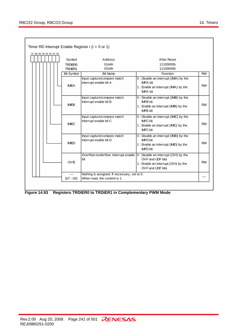
R8C/22 Group, R8C/23 Group 14. Timers
Rev.2.00 Aug 20, 2008 Page 241 of 501REJ09B0251-0200
Figure 14.93 Registers TRDIER0 to TRDIER1 in Complementary PWM Mode
Timer RD Interrupt Enable Register i (i = 0 or 1)
Symbol Address After ResetTRDIER0TRDIER1
0144h0154h
11100000b11100000b
Bit Symbol Bit Name Function RW
RWOVIE
—(b7 - b5) —
Nothing is assigned. If necessary, set to 0.When read, the content is 1.
Input capture/compare matchinterrupt enable bit C
0 : Disable an interrupt (IMIC) by the IMFC bit1 : Enable an interrupt (IMIC) by the IMFC bit
IMIEC RW
RW
Input capture/compare matchinterrupt enable bit D
0 : Disable an interrupt (IMID) by the IMFD bit1 : Enable an interrupt (IMID) by the IMFD bit
Overflow /underflow interrupt enablebit
0 : Disable an interrupt (OVI) by the OVF and UDF bits1 : Enable an interrupt (OVI) by the OVF and UDF bits
RW
IMIEB RW
Input capture/compare matchinterrupt enable bit A
0 : Disable an interrupt (IMIA) by the IMFA bit1 : Enable an interrupt (IMIA) by the IMFA bit
Input capture/compare matchinterrupt enable bit B
0 : Disable an interrupt (IMIB) by the IMFB bit1 : Enable an interrupt (IMIB) by the IMFB bit
IMIEA
b7 b6 b5 b4 b3 b2
IMIED
b1 b0

R8C/22 Group, R8C/23 Group 14. Timers
Rev.2.00 Aug 20, 2008 Page 242 of 501REJ09B0251-0200
Figure 14.94 Registers TRD0 to TRD1 in Complementary PWM Mode
Figure 14.95 Registers TRDGRAi, TRDGRBi, TRDGRC1 and TRDGRDi in Complementary PWM Mode
The following registers are disabled in the complementary PWM mode:TRDPMR, TRDOCR, TRDDF0, TRDDF1, TRDIORA0, TRDIORC0, TRDPOCR0, TRDIORA1, TRDIORC1and TRDPOCR1
Timer RD Counter 0(1)
Symbol Address After ResetTRD0 0147h-0146h 0000h
Setting Range RW
NOTE:1.
FunctionSet the dead time.Count a count source. Count operation is incremented or decremented.When an overf low occurs, the OVF bit in the TRDSR0 register is set to 1.
0000h to FFFFh RW
Access the TRD0 register in 16-bit units. Do not access it in 8-bit units.
b0b7(b8)
b0(b15)
b7
Timer RD Counter 1(1)
Symbol Address After ResetTRD1 0157h-0156h 0000h
Setting Range RW
NOTE:1.
(b8)b0
(b15)b7
Access the TRD1 register in 16-bit units. Do not access it in 8-bit units.
b0b7
FunctionSelect 0000h.Count a count source. Count operation is incremented or decremented.When an underf low occurs, the UDF bit in the TRDSR1 register is set to 1.
0000h to FFFFh RW
Timer RD General Register Ai, Bi, C1 and Di (i = 0 or 1)(1,2)
Symbol Address After ResetTRDGRA0TRDGRB0TRDGRD0TRDGRA1TRDGRB1TRDGRC1TRDGRD1
0149h-0148h014Bh-014Ah014Fh-014Eh0159h-0158h015Bh-015Ah015Dh-015Ch015Fh-015Eh
FFFFhFFFFhFFFFhFFFFhFFFFhFFFFhFFFFh
RW
NOTES:1.2. The TRDGRC0 register is not used in complementary PWM mode.
RW
FunctionRefer to Table 14.32 TRDGRji Register Functions in Complementary PWM Mode
Access the TRDGRAi to TRDGRDi registers in 16-bit units. Do not access them in 8-bit units.
b0b7(b8)
b0(b15)
b7

R8C/22 Group, R8C/23 Group 14. Timers
Rev.2.00 Aug 20, 2008 Page 243 of 501REJ09B0251-0200
BFC0, BFD0, BFC1, BFD1: Bits in TRDMR register
Since values cannot be written to the TRDGRB0, TRDGRA1, or TRDGRB1 register directly after countoperation starts (prohibited item), use the TRDGRD0, TRDGRC1, or TRDGRD1 register as a buffer register.However, to write data to the TRDGRD0, TRDGRC1, or TRDGRD1 register, set bits BFD0, BFC1, and BFD1to 0 (general register). After this, bits BFD0, BFC1, and BFD1 may be set to 1 (buffer register).
Table 14.32 TRDGRji Register Functions in Complementary PWM ModeRegister Setting Register Function PWM Output Pin
TRDGRA0 − General register. Set the PWM period at initialization.Setting range: Setting value or above in TRD0 register FFFFh - TRD0 register setting value or belowDo not write when the TSTART0 and TSTART1 bits in the TRDSTR register are set to 1 (count starts).
(Output inversed every half period of TRDIOC0 pin)
TRDGRB0 − General register. Set the changing point of PWM1 output at initialization.Setting range: Setting value or above in TRD0 register TRDGRA0 register - TRD0 register setting value or belowDo not write when the TSTART0 and TSTART1 bits in the TRDSTR register are set to 1 (count starts).
TRDIOB0TRDIOD0
TRDGRA1 − General register. Set the changing point of PWM2 output at initialization.Setting range: Setting value or above in TRD0 register TRDGRA0 register - TRD0 register setting value or belowDo not write when the TSTART0 and TSTART1 bits in the TRDSTR register are set to 1 (count starts).
TRDIOA1TRDIOC1
TRDGRB1 − General register. Set the changing point of PWM3 output at initialization.Setting range: Setting value or above in TRD0 register TRDGRA0 register - TRD0 register setting value or belowDo not write when the TSTART0 and TSTART1 bits in the TRDSTR register are set to 1 (count starts).
TRDIOB1TRDIOD1
TRDGRC0 − These registers not used in complementary PWM mode. −
TRDGRD0 BFD0 = 1 Buffer register. Set the changing point of next PWM1 output.(Refer to 14.3.2 Buffer Operation)Setting range: Setting value or above in TRD0 register TRDGRA0 register - TRD0 register setting value or belowSet this register to the same value as the TRDGRB0 register for the initialization.
TRDIOB0TRDIOD0
TRDGRC1 BFC1 = 1 Buffer register. Set the changing point of next PWM2 output.(Refer to 14.3.2 Buffer Operation)Setting range: Setting value or above in TRD0 register TRDGRA0 register - TRD0 register setting value or belowSet this register to the same value as the TRDGRA1 register for the initialization.
TRDIOA1TRDIOC1
TRDGRD1 BFD1 = 1 Buffer register. Set the changing point of next PWM3 output.(Refer to 14.3.2 Buffer Operation)Setting range: Setting value or above in TRD0 register TRDGRA0 register - TRD0 register setting value or belowSet this register to the same value as the TRDGRB1 register for the initialization.
TRDIOB1TRDIOD1

R8C/22 Group, R8C/23 Group 14. Timers
Rev.2.00 Aug 20, 2008 Page 244 of 501REJ09B0251-0200
Figure 14.96 Output Model of Complementary PWM Mode
Value in TRDi register
TRDIOD0 output
0000h
Value in TRDGRA0register
Value in TRDGRB0register
Value in TRDGRA1register
Value in TRDGRB1register
TRDIOB0 output
TRDIOC1 output
TRDIOA1 output
TRDIOD1 output
TRDIOB1 output
TRDIOC0 output
Value in TRD0 register
Value in TRD1 register
i = 0 or 1

R8C/22 Group, R8C/23 Group 14. Timers
Rev.2.00 Aug 20, 2008 Page 245 of 501REJ09B0251-0200
Figure 14.97 Operating Example of Complementary PWM Mode
m + 2 - p
p
n + 1
n + 1 - p p n + 1 - p
n
n
n
m - p - n + 1
m
n
Value in TRDi register
Count source
TRDIOD0 output
p
m: Setting Value in TRDGRA0 registern: Setting Value in TRDGRB0 registerp: Setting Value in TRD0 register
TRDIOB0 output
IMFA bit inTRDSR0 register
1
0
TRDGRB0 register
TSTART0 and TSTART1bits in TRDSTR register
1
0
TRDIOC0 output
0000h
m + 1
(m - p - n + 1) × 2Width of normal-
phase active level
Deadtime
(n + 1 - p) × 2Width of counter-phase active level
Set toFFFFh
1
0
UDF bit inTRDSR1 register
1
0
Following data
Modify with a program
TRDGRD0 register
Transfer (When the CMD1 to CMD0 bits are set to 11b) Transfer (When the CMD1 to CMD0 bits are set to 10b)
Value in TRD1 register
Value in TRD0 register
CMD0, CMD1: Bits in TRDFCR register
i = 0 or 1
The above applies to the following conditions:The OLS1 and OLS0 bits in the TRDFCR are set to 0 (initial output level “H”, active level “L” for normal-phase and counter-phase)
Set to 0 by a program
Active level “L”
Initial output “H”
Initial output “H”
Set to 0 by a program
Set to 0 by a programIMFB bit inTRDSR0 register

R8C/22 Group, R8C/23 Group 14. Timers
Rev.2.00 Aug 20, 2008 Page 246 of 501REJ09B0251-0200
14.3.9.1 Transfer Timing from Buffer Register• Transfer from the TRDGRD0, TRDGRC1 and TRDGRD1 registers to the TRDGRB0, TRDGRA1 and
TRDGRB1 registersWhen the CMD1 to CMD0 bits in the TRDFCR register are set to 10b, the content is transferred when theTRD1 register underflows.When the CMD1 to CMD0 bits are set to 11b, the content is transferred at the compare match in the TRD0and TRDGRA0 registers.
14.3.9.2 A/D Trigger GenerationThe compare match in the TRD0 and TRDGRA0 registers and the TRD1 underflow can be used as aconversion start trigger of the A/D converter. It can be selected by the ADEG and ADTRG bits in the TRDFCRregister.Also, set the ADCAP bit in the ADCON0 register to 1 (starts in Timer RD).

R8C/22 Group, R8C/23 Group 14. Timers
Rev.2.00 Aug 20, 2008 Page 247 of 501REJ09B0251-0200
14.3.10 PWM3 ModeOutput 2 PWM waveforms with the same period.Figure 14.98 shows the Block Diagram of PWM3 Mode, Table 14.33 lists the PWM3 Mode Specifications.Figures 14.99 to 14.107 show the Registers Associated with PWM3 Mode and Figure 14.108 shows theOperating Example of PWM3 Mode.
Figure 14.98 Block Diagram of PWM3 Mode
TRDIOA0 Outputcontrol
TRDGRC0
Compare match signal
TRDIOB0 Outputcontrol
Comparator TRDGRA0TRD0
TRDGRC1
Compare match signal
Comparator TRDGRA1
TRDGRD0Comparator TRDGRB0
TRDGRD1Comparator TRDGRB1
Compare match signal
Compare match signal
Buffer

R8C/22 Group, R8C/23 Group 14. Timers
Rev.2.00 Aug 20, 2008 Page 248 of 501REJ09B0251-0200
i = 0 or 1, j = either A, B, C or D
Table 14.33 PWM3 Mode SpecificationsItem Specification
Count Sources f1, f2, f4, f8, f32, fOCO40MCount Operations The TRD0 register is incremented. (The TRD1 is not used.)PWM Waveform PWM period: 1/fk × (m + 1)
Active level width of TRDIOA0 output: 1/fk × (m - n)Active level width of TRDIOB0 output: 1/fk × (p - q) fk: Frequency of count source m: Setting value in the TRDGRA0 register n: Setting value in the TRDGRA1 register p: Setting value in the TRDGRB0 register q: Setting value in the TRDGRB1 register
Count Start Condition Write 1 (count starts) to the TSTART0 bit in the TRDSTR register.Count Stop Conditions • Write 0 (count stops) to the TSTART0 bit in the TRDSTR register
when the CSEL0 bit in the TRDSTR register is set to 1.The PWM output pin holds output level before the count stops
• When the CSEL0 bit in the TRDSTR register is set to 0, the count stops at the compare match in the TRDGRA0 register.The PWM output pin holds level after output change by the compare match.
Interrupt Request Generation Timing
• Compare match (the content in the TRDi register matches with the content in the TRDGRji register.)
• The TRD0 register overflowsTRDIOA0, TRDIOB0 Pin Functions
PWM output
TRDIOC0, TRDIOD0, TRDIOA1 to TRDIOD1 Pin Functions
Programmable I/O port
INT0 Pin Function Programmable I/O port, pulse output forced cutoff signal input or INT0 interrupt input
Read from Timer The count value can be read by reading the TRD0 register.Write to Timer The value can be written to the TRD0 register.Selection Functions • Pulse output forced cutoff signal input (refer to 14.3.4 Pulse Output
Forced Cutoff)• Select the active level every pin.• Buffer operation (refer to 14.3.2 Buffer Operation)
m + 1
TRDIOA0 output
TRDIOB0 output
(When “H” is selected for the active level)
p - q
m - n
n + 1
p + 1
q + 1

R8C/22 Group, R8C/23 Group 14. Timers
Rev.2.00 Aug 20, 2008 Page 249 of 501REJ09B0251-0200
Figure 14.99 TRDSTR Register in PWM3 Mode
Timer RD Start Register(1)
Symbol Address After ResetTRDSTR 0137h 11111100b
Bit Symbol Bit Name Function RW
NOTES:1.
2.3.4.5.
When the CSEL0 bit is set to 1, w rite 0 to the TSTART0 bit.When the CSEL1 bit is set to 1, w rite 0 to the TSTART1 bit.When the CSEL0 bit is set to 0 and generating the compare match signal(TRDIOA0), this bit is set to 0 (count stops).When the CSEL1 bit is set to 0 and generating the compare match signal(TRDIOA1), this bit is set to 0 (count stops).
b3 b2
CSEL1
b1 b0
0
TSTART0
b7 b6 b5 b4
RW
TSTART1 RWTRD1 count start f lag(5) Set this bit to 0 (count stops) in PWM3
mode(3)
TRD0 count start f lag(4) 0 : Count stops(2)
1 : Count starts
TRD0 count operation select bit 0 : Count stops at the compare match w ith the TRDGRA0 register1 : Count continues at the compare match w ith the TRDGRA0 register
CSEL0 RW
—(b7 - b4)
Nothing is assigned. If necessary, set to 0.When read, the content is 1.
Set the TRDSTR register using the MOV instruction (do not use the bit handling instruction). Refer to 14.3.12.1TRDSTR Register of Notes on Timer RD.
RW
TRD1 count operation select bit 0 : Count stops at the compare match w ith the TRDGRA1 register1 : Count continues at the compare match w ith the TRDGRA1 register
—

R8C/22 Group, R8C/23 Group 14. Timers
Rev.2.00 Aug 20, 2008 Page 250 of 501REJ09B0251-0200
Figure 14.100 Registers TRDMR and TRDFCR in PWM3 Mode
Timer RD Mode Register
Symbol Address After ResetTRDMR 0138h 00001110b
Bit Symbol Bit Name Function RW
b3 b2
BFD0
b1 b0
SYNC
b7 b6 b5 b4
RW
—(b3 - b1) —
Timer RD synchronous bit This bit is disabled in PWM3 mode.
Nothing is assigned. If necessary, set to 0.When read, the content is 1.
RWTRDGRD0 register functionselection bit
0 : General register1 : Buffer register of TRDGRB0 register
TRDGRC1 register functionselection bit
0 : General register1 : Buffer register of TRDGRA1 register RW
TRDGRC0 register functionselection bit
0 : General register1 : Buffer register of TRDGRA0 registerBFC0 RW
RW
BFC1
BFD1TRDGRD1 register functionselection bit
0 : General register1 : Buffer register of TRDGRB1 register
Timer RD Function Control Register
Symbol Address After ResetTRDFCR 013Ah 10000000b
Bit Symbol Bit Name Function RW
NOTES:1.2.
STCLKExternal clock input selection bit Set this bit to 0 (external clock input
disabled) in PWM3 mode. RW
RW
PWM3 RW
ADTRG
ADEGA/D trigger edge selection bit(enabled in complementary PWM mode)
This bit is disabled in PWM3 mode.RW
PWM3 mode selection bit(2) Set this bit to 0 (PWM3 mode) in PWM3mode.
Normal-phase output level selection bit(enabled in reset synchronous PWMmode or complementary PWM mode)
This bit is disabled in PWM3 mode.
Set bits CMD1 to CMD0 w hen both the TSTART0 and TSTART1 bits in the TRDSTR register are set to 0 (count stops).
OLS0 RW
RWCounter-phase output level selection bit(enabled in reset synchronous PWMmode or complementary PWM mode)
This bit is disabled in PWM3 mode.
A/D trigger enable bit(enabled in complementary PWM mode)
This bit is disabled in PWM3 mode.
RW
CMD1 RW
Combination mode selection bit(1) Set to 00b (timer mode, PWM mode, orPWM3 mode) in PWM3 mode.CMD0
b7 b6 b5 b4
0 0
When bits CMD1 to CMD0 are set to 00b (timer mode, PWM mode, or PWM3 mode), the setting of the PWM3 bit isenabled.
b3 b2
OLS1
b1 b0
0 0

R8C/22 Group, R8C/23 Group 14. Timers
Rev.2.00 Aug 20, 2008 Page 251 of 501REJ09B0251-0200
Figure 14.101 Registers TRDOER1 to TRDOER2 in PWM3 Mode
Timer RD Output Master Enable Register 1
Symbol Address After ResetTRDOER1 013Bh FFhBit Symbol Bit Name Function RW
ED1 RW
EA1EB1 RW
TRDIOD1 output disable bit
TRDIOB1 output disable bitEC1 TRDIOC1 output disable bit
TRDIOD0 output disable bit RWTRDIOA1 output disable bit
RW
RW
Set these bits to 1 (programmable I/O port)in PWM3 mode.
TRDIOC0 output disable bitEC0 RW
RW
EB0 RW
TRDIOA0 output disable bit 0 : Enable output1 : Disable output (The TRDIOA0 pin is used as a programmable I/O port.)
TRDIOB0 output disable bit 0 : Enable output1 : Disable output (The TRDIOB0 pin is used as a programmable I/O port.)
1 1 1 1b7 b6 b5 b4 b3 b2
ED0
b1 b0
1 1
EA0
Timer RD Output Master Enable Register 2
Symbol Address After ResetTRDOER2 013Ch 01111111bBit Symbol Bit Name Function RW
INT0_____
of pulse output forced 0 : Pulse output forced cutoff input disabled1 : Pulse output forced cutoff input enabled (All bits in the TRDOER1 register are set to 1 (disable output) w hen “L” is applied to the INT0
_____ pin)
NOTE:1. Refer to 14.3.4 Pulse Output Forced Cutoff.
——
(b6 - b0)Nothing is assigned. If necessary, set to 0.When read, the content is 1.
RWPTO
cutoff signal input enabledbit(1)
b7 b6 b5 b4 b3 b2 b1 b0

R8C/22 Group, R8C/23 Group 14. Timers
Rev.2.00 Aug 20, 2008 Page 252 of 501REJ09B0251-0200
Figure 14.102 TRDOCR Register in PWM3 Mode
Timer RD Output Control Register(1)
Symbol Address After ResetTRDOCR 013Dh 00h
Bit Symbol Bit Name Function RW
NOTES:1.
2. When the pin functions are w aveform output (refer to Table 14.12 and 14.13) and the TRDOCR register is set, theinitial output level is output.
TOA1
TOB1 RW
TRDIOD1 initial output levelselection bit
TRDIOB1 initial output levelselection bit
TOC1TRDIOC1 initial output levelselection bit
This bit is disabled in PWM3 mode.TRDIOC0 initial output levelselection bit
Write to the TRDOCR register w hen both the TSTART0 and TSTART1 bits in the TRDSTR register are set to 0 (countstops).
TOC0 RW
RW
TRDIOA1 initial output levelselection bit
RW
RW
TRDIOD0 initial output levelselection bit
TOD1 RW
RW
TOB0 RW
TRDIOA0 output levelselection bit(2)
0 : Active level “H”, initial output “L”, output “H” by the compare match in the TRDGRA1register, output “L” by the compare match in the TRDGRA0 register1 : Active level “L”, initial output “H”, output “L” by the compare match in the TRDGRA1register, output “H” by the compare match in the TRDGRA0 register
TRDIOB0 output levelselection bit(2)
0 : Active level “H”, initial output “L”, output “H” by the compare match in the TRDGRB1register, output “L” by the compare match in the TRDGRB0 register1 : Active level “L”, initial output “H”, output “L” by the compare match in the TRDGRB1register, output “H” by the compare match in the TRDGRB0 register
b7 b6 b5 b4 b3 b2
TOD0
b1 b0
TOA0

R8C/22 Group, R8C/23 Group 14. Timers
Rev.2.00 Aug 20, 2008 Page 253 of 501REJ09B0251-0200
Figure 14.103 TRDCR0 Register in PWM3 Mode
Timer RD Control Register i (i = 0 or 1)(2)
Symbol Address After ResetTRDCR0 0140h 00h
Bit Symbol Bit Name Function RW
NOTES: 1.
2.
RW
TCK1 RW
TCK0
RW
RWRW
CCLR2CCLR1 RW
Count source selection bit b2 b1b0
0 0 0 : f10 0 1 : f20 1 0 : f40 1 1 : f81 0 0 : f321 0 1 : Do not set1 1 0 : fOCO40M1 1 1 : Do not set
External clock edge selectionbit(1)
This bit is disabled in PWM3 mode.
b7 b6 b5 b4
0 0 1b3 b2
CKEG0
b1 b0
TCK2
The TRDCR1 register is not used in PWM3 mode.
RW
CKEG1CCLR0 RWSet to 001b (the TRD0 register clear at the
compare match w ith TRDGRA0 register) inPWM3 mode.
TRD0 counter clear selection bit
This bit is enabled w hen the TCK2 to TCK0 bits are set to 101b (TRDCLK input) and the STCLK bit in the TRDFCRregister is set to 1 (external clock input enabled).

R8C/22 Group, R8C/23 Group 14. Timers
Rev.2.00 Aug 20, 2008 Page 254 of 501REJ09B0251-0200
Figure 14.104 Registers TRDSR0 and TRDSR1 in PWM3 Mode
Timer RD Status Register i (i = 0 or 1)
Symbol Address After ResetTRDSR0 0143h 11100000bTRDSR1 0153h 11000000b
Bit Symbol Bit Name Function RW
NOTES:1.
2.
b2
IMFD
b1 b0
RW
b7 b6 b5 b4 b3
RW
IMFB RW
Input capture/compare match f lag A [Source for setting this bit to 0]Write 0 after read.(1)
[Source for setting this bit to 1]When the value in the TRDi registermatches w ith the value in the TRDGRAiregister.
Input capture/compare match f lag B [Source for setting this bit to 0]Write 0 after read.(1)
[Source for setting this bit to 1]When the value in the TRDi registermatches w ith the value in the TRDGRBiregister.
IMFA
OVF
Input capture/compare match f lag C [Source for setting this bit to 0]Write 0 after read.(1)
[Source for setting this bit to 1]When the value in the TRDi registermatches w ith the value in the TRDGRCiregister.(2)
IMFC
Overflow f lag [Source for setting this bit to 0]Write 0 after read.(1)
[Source for setting this bit to 1]When the TRDi register overf low s.
RW
RW
Input capture/compare match f lag D [Source for setting this bit to 0]Write 0 after read.(1)
[Source for setting this bit to 1]When the value in the TRDi registermatches w ith the value in the TRDGRDiregister.(2)
Including w hen the BFji bit (j = C or D) in the TRDMR register is set to 1 (TRDGRji is used as the buffer register).
—(b7 - b6) —
Nothing is assigned. If necessary, set to 0.When read, the content is 1.
The w riting results are as follow s:• This bit is set to 0 w hen the read result is 1 and w riting 0 to the same bit.• This bit remains unchanged even if the read result is 0 and w riting 0 to the same bit. (This bit remains 1 even if this bit is set to 1 from 0 after reading, and w riting 0.)• This bit remains unchanged w hen w riting 1.
UDFUnderflow f lag(1) This bit is disabled in PWM3 mode.
RW

R8C/22 Group, R8C/23 Group 14. Timers
Rev.2.00 Aug 20, 2008 Page 255 of 501REJ09B0251-0200
Figure 14.105 Registers TRDIER0 and TRDIER1 in PWM3 Mode
Figure 14.106 TRD0 Register in PWM3 Mode
Timer RD Interrupt Enable Register i (i = 0 or 1)
Symbol Address After ResetTRDIER0 0144h 11100000bTRDIER1 0154h 11100000b
Bit Symbol Bit Name Function RW
b3 b2
IMIED
b1 b0b7 b6 b5 b4
RW
IMIEB RW
Input capture/compare matchinterrupt enable bit A
0 : Disable an interrupt (IMIA) by the IMFA bit1 : Enable an interrupt (IMIA) by the IMFA bit
Input capture/compare matchinterrupt enable bit B
0 : Disable an interrupt (IMIB) by the IMFB bit1 : Enable an interrupt (IMIB) by the IMFB bit
IMIEA
Input capture/compare matchinterrupt enable bit C
0 : Disable an interrupt (IMIC) by the IMFC bit1 : Enable an interrupt (IMIC) by the IMFC bit
IMIEC RW
RW
Input capture/compare matchinterrupt enable bit D
0 : Disable an interrupt (IMID) by the IMFD bit1 : Enable an interrupt (IMID) by the IMFD bit
Overflow /underflow interrupt enablebit
0 : Disable an interrupt (OVI) by the OVF bit1 : Enable an interrupt (OVI) by the OVF bit
RWOVIE
—(b7 - b5) —
Nothing is assigned. If necessary, set to 0.When read, the content is 1.
Timer RD Counter 0(1,2)
Symbol Address After ResetTRD0 0147h-0146h 0000h
Setting Range RW
NOTES:1.2.
FunctionCount a count source. Count operation is incremented.When an overf low occurs, the OVF bit in the TRDSR0 register is set to 1. 0000h to FFFFh RW
b7
The TRD1 register is not used in PWM3 mode.
(b8)b0
(b15)b7
Access the TRD0 register in 16-bit units. Do not access it in 8-bit units.
b0

R8C/22 Group, R8C/23 Group 14. Timers
Rev.2.00 Aug 20, 2008 Page 256 of 501REJ09B0251-0200
Figure 14.107 Registers TRDGRAi, TRDGRBi, TRDGRCi and TRDGRDi in PWM3 Mode
The following registers are disabled in PWM3 mode:TRDPMR, TRDDF0, TRDDF1, TRDIORA0, TRDIORC0, TRDPOCR0, TRDIORA1, TRDIORC1 andTRDPOCR1
Timer RD General Register Ai, Bi, Ci and Di (i = 0 or 1)(1)
Symbol Address After ResetTRDGRA0TRDGRB0TRDGRC0TRDGRD0TRDGRA1TRDGRB1TRDGRC1TRDGRD1
0149h-0148h014Bh-014Ah014Dh-014Ch014Fh-014Eh0159h-0158h015Bh-015Ah015Dh-015Ch015Fh-015Eh
FFFFhFFFFhFFFFhFFFFhFFFFhFFFFhFFFFhFFFFh
RW
NOTE:1.
RW
FunctionRefer to Table 14.34 TRDGRji Register Functions in PWM3 Mode
Access the TRDGRAi to TRDGRDi registers in 16-bit units. Do not access them in 8-bit units.
b0b7(b8)
b0(b15)
b7

R8C/22 Group, R8C/23 Group 14. Timers
Rev.2.00 Aug 20, 2008 Page 257 of 501REJ09B0251-0200
BFC0, BFD0, BFC1, BFD1: Bits in TRDMR Register
Registers TRDGRC0, TRDGRC1, TRDGRD0, and TRDGRD1 are not used in PWM3 mode. To use them asbuffer registers, set bits BFC0, BFC1, BFD0, and BFD1 to 0 (general register) and write a value to the TRDGRC0,TRDGRC1, TRDGRD0, or TRDGRD1 register. After this, bits BFC0, BFC1, BFD0, and BFD1 may be set to 1(buffer register).
Table 14.34 TRDGRji Register Functions in PWM3 ModeRegister Setting Register Function PWM Output Pin
TRDGRA0 − General register. Set the PWM period.Setting range: Value set in TRDGRA1 register or above
TRDIOA0
TRDGRA1 General register. Set the changing point (the active level timing) of PWM output.Setting range: Value set in TRDGRA0 register or below
TRDGRB0 General register. Set the changing point (the timing that returns to initial output level) of PWM output.Setting range: Value set in TRDGRB1 register or above
Value set in TRDGRA0 register or below
TRDIOB0
TRDGRB1 General register. Set the changing point (active level timing) of PWM output.Setting range: Value set in TRDGRB0 register or below
TRDGRC0 BFC0 = 0 (These registers are not used in PWM3 mode) −TRDGRC1 BFC1 = 0TRDGRD0 BFD0 = 0TRDGRD1 BFD1 = 0TRDGRC0 BFC0 = 1 Buffer register. Set the next PWM period.
(Refer to 14.3.2 Buffer Operation.)Setting range: Value set in TRDGRC1 register or above
TRDIOA0
TRDGRC1 BFC1 = 1 Buffer register. Set the changing point of next PWM output. (Refer to 14.3.2 Buffer Operation.)Setting range: Value set in TRDGRC0 register or below
TRDGRD0 BFD0 = 1 Buffer register. Set the changing point of next PWM output. (Refer to 14.3.2 Buffer Operation.)Setting range: Value set in TRDGRD1 register or above,
setting value or below in TRDGRC0 register.
TRDIOB0
TRDGRD1 BFD1 = 1 Buffer register. Set the changing point of next PWM output. (Refer to 14.3.2 Buffer Operation.)Setting range: Value set in TRDGRD0 register or below

R8C/22 Group, R8C/23 Group 14. Timers
Rev.2.00 Aug 20, 2008 Page 258 of 501REJ09B0251-0200
Figure 14.108 Operating Example of PWM3 Mode
Value in TRD0 register
Count source
TRDIOA0 output
0000h
FFFFh
TRDIOB0 output
m: Setting value in TRDGRA0 registern: Setting value in TRDGRA1 registerp: Setting value in TRDGRB0 registerq: Setting value in TRDGRB1 register
m
n
p
q
TSTART0 bit inTRDSTR register
1
0
Set to 0 by a program Set to 0 by a program
m + 1
n + 1 m - n
p + 1
q + 1 p - q
Count stop
Output “H” by thecompare match in the
TRDGRA1 register
Set to 0 by a programSet to 0 by a program
Set to 0 by a program
Transfer
m
m Following data
Transfer
m
Output “L” by the comparematch in the TRDGRA0 register
Transfer from the buffer registerto general register
Transfer from the buffer registerto general register
Initial output “L”
j = either A or B
The above applies to the following conditions:• Both the TOA0 and TOB0 bits in the TRDOCR register are set to 0 (initial output level “L”, output “H” by the compare match in the
TRDGRj1 register, output “L” by the compare match in the TRDGRj0 register)• The BFC0 bit in the TRDMR register is set to 1 (the TRDGRC0 register is used as the buffer register of the TRDGRA0 register).
CSEL0 bit inTRDSTR register
1
0
IMFA bit inTRDSR0 register
1
0
IMFB bit inTRDSR0 register
1
0
TRDGRA0 register
TRDGRC0 register

R8C/22 Group, R8C/23 Group 14. Timers
Rev.2.00 Aug 20, 2008 Page 259 of 501REJ09B0251-0200
14.3.11 Timer RD InterruptTimer RD generates the Timer RD interrupt request based on 6 sources every channel. The Timer RD interrupthas 1 TRDiIC register (IR bit, ILVL0 to ILVL2 bits) every channel, and 1 vector.Table 14.35 lists the Registers Associated with Timer RD Interrupt and Figure 14.109 shows the Block Diagramof Timer RD Interrupt.
Figure 14.109 Block Diagram of Timer RD Interrupt
As with other maskable interrupts, the timer RD interrupt is controlled by the combination of the I flag, IR bit,bits ILVL0 to ILVL2, and IPL. However, since the interrupt source (timer RD interrupt) is generated by acombination of multiple interrupt request sources, the following differences from other maskable interruptsapply:
• When bits in the TRDSRi register corresponding to bits set to 1 in the TRDIERi register are set to 1 (enableinterrupt), the IR bit in the TRDiIC register is set to 1 (interrupt requested).
• When either bits in the TRDSRi register or bits in the TRDIERi register corresponding to bits in theTRDSRi register, or both of them, are set to 0, the IR bit is set to 0 (interrupt not requested). Therefore,even though the interrupt is not acknowledged after the IR bit is set to 1, the interrupt request will not bemaintained.
• When the conditions of other request sources are met, the IR bit remains 1.• When multiple bits in the TRDIERi register are set to 1, which request source causes an interrupt is
determined by the TRDSRi register.• Since each bit in the TRDSRi register is not automatically set to 0 even if the interrupt is acknowledged, set
each bit to 0 in the interrupt routine. For information on how to set these bits to 0, refer to the descriptionsof the registers used in the different modes (Figures 14.41, 14.56, 14.69, 14.81, 14.92 and 14.104).
Table 14.35 Registers Associated with Timer RD InterruptTimer RD
Status RegisterTimer RD
Interrupt Enable RegisterTimer RD
Interrupt Control RegisterChannel 0 TRDSR0 TRDIER0 TRD0ICChannel 1 TRDSR1 TRDIER1 TRD1IC
Timer RD (channel i)Interrupt request(IR bit in TRDiIC register)
IMFA bitIMIEA bit
IMFB bitIMIEB bit
IMFC bitIMIEC bit
IMFD bitIMIED bit
UDF bitOVF bit
OVIE bit
i = 0 or 1IMFA, IMFB, IMFC, IMFD, OVF, UDF: Bits in TRDSRi registerIMIEA, IMIEB, IMIEC, IMIED, OVIE: Bits in TRDIER register
Channel i

R8C/22 Group, R8C/23 Group 14. Timers
Rev.2.00 Aug 20, 2008 Page 260 of 501REJ09B0251-0200
Refer to Registers TRDSR0 to TRDSR1 in each mode (Figures 14.41, 14.56, 14.69, 14.81, 14.92 and14.104) for the TRDSRi register. Refer to Registers TRDIER0 to TRDIER1 in each mode (Figures 14.42,14.57, 14.70, 14.82, 14.93 and 14.105) for the TRDIERi register.Refer to 12.1.6 Interrupt Control for the TRDiIC register and 12.1.5.2 Relocatable Vector Tables for theinterrupt vector.
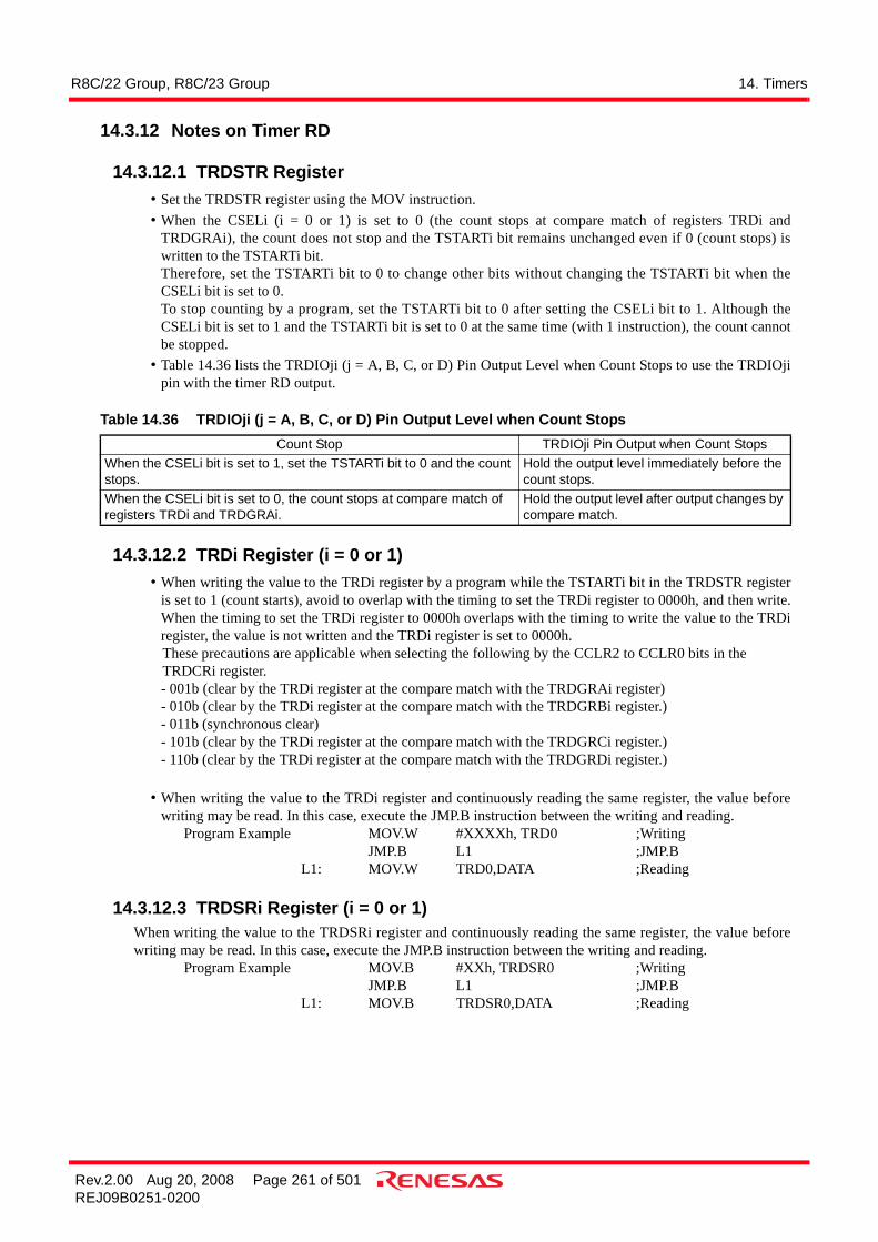
R8C/22 Group, R8C/23 Group 14. Timers
Rev.2.00 Aug 20, 2008 Page 261 of 501REJ09B0251-0200
14.3.12 Notes on Timer RD
14.3.12.1 TRDSTR Register• Set the TRDSTR register using the MOV instruction.• When the CSELi (i = 0 or 1) is set to 0 (the count stops at compare match of registers TRDi and
TRDGRAi), the count does not stop and the TSTARTi bit remains unchanged even if 0 (count stops) iswritten to the TSTARTi bit.Therefore, set the TSTARTi bit to 0 to change other bits without changing the TSTARTi bit when theCSELi bit is set to 0.To stop counting by a program, set the TSTARTi bit to 0 after setting the CSELi bit to 1. Although theCSELi bit is set to 1 and the TSTARTi bit is set to 0 at the same time (with 1 instruction), the count cannotbe stopped.
• Table 14.36 lists the TRDIOji (j = A, B, C, or D) Pin Output Level when Count Stops to use the TRDIOjipin with the timer RD output.
14.3.12.2 TRDi Register (i = 0 or 1)• When writing the value to the TRDi register by a program while the TSTARTi bit in the TRDSTR register
is set to 1 (count starts), avoid to overlap with the timing to set the TRDi register to 0000h, and then write.When the timing to set the TRDi register to 0000h overlaps with the timing to write the value to the TRDiregister, the value is not written and the TRDi register is set to 0000h.
These precautions are applicable when selecting the following by the CCLR2 to CCLR0 bits in the TRDCRi register.- 001b (clear by the TRDi register at the compare match with the TRDGRAi register)- 010b (clear by the TRDi register at the compare match with the TRDGRBi register.)- 011b (synchronous clear)- 101b (clear by the TRDi register at the compare match with the TRDGRCi register.)- 110b (clear by the TRDi register at the compare match with the TRDGRDi register.)
• When writing the value to the TRDi register and continuously reading the same register, the value beforewriting may be read. In this case, execute the JMP.B instruction between the writing and reading.
Program Example MOV.W #XXXXh, TRD0 ;WritingJMP.B L1 ;JMP.B
L1: MOV.W TRD0,DATA ;Reading
14.3.12.3 TRDSRi Register (i = 0 or 1)When writing the value to the TRDSRi register and continuously reading the same register, the value beforewriting may be read. In this case, execute the JMP.B instruction between the writing and reading.
Program Example MOV.B #XXh, TRDSR0 ;WritingJMP.B L1 ;JMP.B
L1: MOV.B TRDSR0,DATA ;Reading
Table 14.36 TRDIOji (j = A, B, C, or D) Pin Output Level when Count StopsCount Stop TRDIOji Pin Output when Count Stops
When the CSELi bit is set to 1, set the TSTARTi bit to 0 and the count stops.
Hold the output level immediately before the count stops.
When the CSELi bit is set to 0, the count stops at compare match of registers TRDi and TRDGRAi.
Hold the output level after output changes by compare match.

R8C/22 Group, R8C/23 Group 14. Timers
Rev.2.00 Aug 20, 2008 Page 262 of 501REJ09B0251-0200
14.3.12.4 Count Source Switch• When switching the count source, switch it after the count stops.
Change procedure(1) Set the TSTARTi (i = 0 or 1) bit in the TRDSTR register to 0 (count stops).(2) Change the TCK2 to TCK0 bits in the TRDCRi register.
• When changing the count source from fOCO40M to the other and stopping fOCO40M, wait 2 cycles ormore of f1 after setting the clock switch, and then stop fOCO40M.
Change procedure(1) Set the TSTARTi (i = 0 or 1) bit in the TRDSTR register to 0 (count stops).(2) Change the TCK2 to TCK0 bits in the TRDCRi register.(3) Wait 2 cycles or more of f1.(4) Set the FRA00 bit in the FRA0 register to 0 (high-speed on-chip oscillator stops).
14.3.12.5 Input Capture Function• Set the pulse width of input capture signal to 3 cycles or more of the Timer RD operation clock. (Refer to
Table 14.11 Timer RD Operation Clocks.)• The value in the TRDi register is transferred to the TRDGRji register after 2 to 3 cycles of the Timer RD
operation clock since the input capture signal is applied to the TRDIOji pin (i = 0 or 1, j = either A, B, C orD) (no digital filter).
14.3.12.6 Reset Synchronous PWM Mode • When reset synchronous PWM mode is used for motor control, use it with OLS0 = OLS1.• Set to reset synchronous PWM mode in the following procedure:
Change procedure(1) Set the TSTART0 bit in the TRDSTR register to 0 (count stops).(2) Set the CMD1 to CMD0 bits in the TRDFCR register to 00b (timer mode, PWM mode, and PWM3
mode).(3) Set the CMD1 to CMD0 bits to 01b (reset synchronous PWM mode).(4) Set the registers associated with other Timer RD again.
14.3.12.7 Complementary PWM Mode• When complementary PWM mode is used for motor control, use it with OLS0 = OLS1.• Change the CMD1 to CMD0 bits in the TRDFCR register in the following procedure.
Change procedure: When setting to complementary PWM mode (including re-set), or changing the transfer timing from the buffer register to the general register in complementary PWM mode.
(1) Set both the TSTART0 and TSTART1 bits in the TRDSTR register to 0 (count stops).(2) Set the CMD1 to CMD0 bits in the TRDFCR register to 00b (timer mode, PWM mode, and PWM3
mode)(3) Set the DMD1 to CMD0 bits to 10b or 11b (complementary PWM mode).(4) Set the registers associated with other Timer RD again.
Change procedure: When stopping complementary PWM mode(1) Set both the TSTART0 and CSEL1 bits in the TRDSTR register to 0 (count stops).(2) Set the CMD1 to CMD bits to 00b (other than reset synchronous PWM mode, complementary PWM
mode)
• Do not write to the TRDGRA0, TRDGRB0, TRDGRA1 and TRDGRB1 registers during operation.When changing the PWM waveform, transfer the value written to the TRDGRD0, TRDGRC1 andTRDGRD1 registers to the TRDGRB0, TRDGRA1 and TRDGRB1 registers using the buffer operation.However, to write data to the TRDGRD0, TRDGRC1, or TRDGRD1 register, set bits BFD0, BFC1, andBFD1 to 0 (general register). After this, bits BFD0, BFC1, and BFD1 may be set to 1 (buffer register).The PWM period cannot be changed.

R8C/22 Group, R8C/23 Group 14. Timers
Rev.2.00 Aug 20, 2008 Page 263 of 501REJ09B0251-0200
• When the value in the TRDGRA0 register is assumed as m, the TRD0 register counts order of m - 1, m, m+ 1, m, m - 1 when changing from increment to decrement. When changing from m to m + 1, the IMFA bit is set to 1. Also, the CMD1 to CMD0 bits in the TRDFCRregister are set to 11b (complementary PWM mode, buffer data transferred by the compare match in theTRD0 and TRDGRA0 registers), the content in the buffer register (TRDGRD0, TRDGRC1, TRDGRD1) istransferred to the general register (TRDGRB0, TRDGRA1, TRDGRB1). For the order of m + 1, m, m - 1 operation, the IMFA bit remains unchanged and data are not transferred tothe register such as the TRDGRA0 register.
Figure 14.110 Operation at Compare Match between Registers TRD0 and TRDGRA0 in Complementary PWM Mode
No changeIMFA bit in
TRDSR0 register
Transferred frombuffer register
TRDGRB0 registerTRDGRA1 registerTRDGRB1 register
Count value in TRD0register
Setting value inTRDGRA0
register m
m + 1
Set to 0 by a program
Not transferred from buffer register
When the CMD1 to CMD0 bits in theTRDFCR register are set to 11b.(Transfer from the buffer register to thegeneral register at the compare matchof the TRD0 register and TRDGRA0register)
1
0

R8C/22 Group, R8C/23 Group 14. Timers
Rev.2.00 Aug 20, 2008 Page 264 of 501REJ09B0251-0200
• The TRD1 register counts the order of 1, 0, FFFFh, 0, 1 when changing from decrement to increment.The UDF bit is set to 1 by the order of 1, 0, FFFFh operation. Also, when the CMD1 to CMD0 bits in theTRDFCR register are set to 10b (complementary PWM mode, buffer data transferred by the underflow inthe TRD1 register), the content in the buffer register (TRDGRD0, TRDGRC1, TRDGRD1) is transferredto the general register (TRDGRB0, TRDGRA1, TRDGRB1). For the order of FFFFh, 0, 1 operation, dataare not transferred to the register such as the TRDGRB0 register. Also, at this time, the OVF bit remainsunchanged.
Figure 14.111 Operation When TRD1 Register Underflows in Complementary PWM Mode
No change
UDF bit inTRDSR0 register
Transferred frombuffer register
TRDGRB0 registerTRDGRA1 registerTRDGRB1 register
Count value in TRD0register
Set to 0 by a program
Not transferred from buffer registerWhen the CMD1 to CMD0 bits in theTRDFCR register are set to 10b.(Transfer from the buffer register to thegeneral register when the TRD1 registerunderflows)
OVF bit inTRDSR0 register
FFFFh
10
1
0
0
1

R8C/22 Group, R8C/23 Group 14. Timers
Rev.2.00 Aug 20, 2008 Page 265 of 501REJ09B0251-0200
• Select with the CMD1 to CMD0 bits for the data transfer timing from the buffer register to the generalregister. However, transfer with the following timing in spite of the value of the CMD1 to CMD0 bits forthe following cases:
Value in buffer register ≥ Value in TRDGRA0 register:Transfer at the underflow in the TRD1 register.And then, when setting the buffer register to 0001h or above and the smaller value than the one in theTRDGRA0 register, and the TRD1 register underflows in the fist time after setting, the value is transferredto the general register. After that, transfer the value with the timing selected by the CMD1 to CMD0 bits.
Figure 14.112 Operation When Value in Buffer Register ≥ Value in TRDGRA0 Register in Complementary PWM Mode
0000h
TRDGRD0 register
TRDIOB0 output
n3n2
m + 1
n3
n2
n1
n2 n1
n3n2 n2 n1n1TRDGRB0 register
Transfer
Transfer byunderflow in TRD1register because ofn3 > m
Transfer byunderflow in TRD1register becauseof first setting ton2 < m
TRDIOD0 output
m: Setting Value in TRDGRA0 Register
The above applies to the following conditions:• The CMD1 to CMD0 bits in the TRDFCR register are set to 11b. (Data in the buffer register is transferred at the compare match in the TRD0 and TRDGRA0 registers in complementary
PWM mode.)• Both the OSL0 and OLS1 bits in the TRDFCR are set to 1. (active ‘H” for normal-phase and counter-phase)
Count value in TRD0register
Count value in TRD1register
Transfer with timing set byCMD1 to CMD0 bits
Transfer with timing set byCMD1 to CMD0 bits
Transfer Transfer Transfer

R8C/22 Group, R8C/23 Group 14. Timers
Rev.2.00 Aug 20, 2008 Page 266 of 501REJ09B0251-0200
When the value in the buffer register is set to 0000h:Transfer by the compare match in the TRD0 and TRDGRA0 registers.And then, when setting the buffer register to 0001h or above and the smaller value than the one in theTRDGRA0 register, and the compare match in the TRD0 and TRDGRA0 registers in the fist time aftersetting, the value is transferred to the general register. After that, transfer the value with the timing selectedby the CMD1 to CMD0 bits.
Figure 14.113 Operation When Value in Buffer Register Is Set to 0000h in Complementary PWM Mode
14.3.12.8 Count Source fOCO40MThe count source fOCO40M can be used with supply voltage VCC = 3.0 to 5.5 V. For supply voltage other thanthat, do not set bits TCK2 to TCK0 in registers TRDCR0 and TRDCR to 110b (select fOCO40M as the countsource).
0000h
TRDGRD0 register
TRDIOB0 output
n1
m + 1
n 2
n1
0000h n1
0000hn1 n1n2TRDGRB0 register
Transfer
Transfer bycompare match inTRD0 andTRDGRA0 registersbecause content inTRDGRD0 registeris set to 0000h.
Transfer bycompare match inTRD0 andTRDGRA0registers becauseof first setting to0001h ≤ n1 < m
Transfer with timingset by CMD1 toCMD0 bits
TRDIOD0 output
m: Setting Value in TRDGRA0 Register
The above applies to the following conditions:• The CMD1 to CMD0 bits in the TRDFCR register are set to 10b. (Data in the buffer register is transferred at the underflow in the TRD1 register in PWM mode.)• Both the OLS0 and OLS1 bits in the TRDFCR register are set to “1” (active “H” for normal-phase and counter-phase).
Count value in TRD0 register
Count value in TRD1 register
Transfer with timingset by CMD1 toCMD0 bits
Transfer Transfer Transfer

R8C/22 Group, R8C/23 Group 14. Timers
Rev.2.00 Aug 20, 2008 Page 267 of 501REJ09B0251-0200
14.4 Timer RETimer RE has the 4-bit counter and 8-bit counter. Timer RE has the following mode:
• Output compare mode Count a count source and detect the compare match
The count source for timer RE is the operating clock that regulates the timing of timer operations.

R8C/22 Group, R8C/23 Group 14. Timers
Rev.2.00 Aug 20, 2008 Page 268 of 501REJ09B0251-0200
14.4.1 Output Compare ModeThe output compare mode is to count the internal count source divided-by-2 using the 4-bit or 8-bit counter anddetect the compare value match with the 8-bit counter.Figure 14.114 shows the Block Diagram of Output Compare Mode and Table 14.37 lists the Output CompareMode Specifications. Figures 14.115 to 14.119 show the Registers Associated with Output Compare Mode andFigure 14.120 shows the Operation in Output Compare Mode.
Figure 14.114 Block Diagram of Output Compare Mode
TOENA
TREO pin
f32
f4f8
4-bitcounter 8-bit
counter
TRESEC
Comparisoncircuit
TREMIN
1/2RCS2 = 1
RCS2 = 0
COMIETimer RE interrupt
f2
Matchsignal
= 00b
= 01b
= 10b
RCS1 to RCS0
RCS6 to RCS5= 00b
= 01b
= 10b
= 11b
TOENA, TRERST: Bits in TRECR1 registerCOMIE: Bit in TRECR2 registerRCS0 to RCS2, RCS5 to RCS6: Bits in TRECSR register
T Q
RResetTRERST bit
Data bus

R8C/22 Group, R8C/23 Group 14. Timers
Rev.2.00 Aug 20, 2008 Page 269 of 501REJ09B0251-0200
Table 14.37 Output Compare Mode SpecificationsItem Specification
Count Source f4, f8, f32Count Operation • Increment
• When the 8-bit counter content matches with the TREMIN register content, the value returns to 00h and count continues.The count value is held while count stops.
Count Period • When RCS2 = 0 (4-bit counter is not used)1/fi x 2 x (n + 1)
• When RCS2 = 1 (4-bit counter is used)1/fi x 32 x (n + 1)
fi: Frequency of count sourcen: Setting value of TREMIN register
Count Start Condition Write 1 (count starts) to the TSTART bit in the TRECR1 registerCount Stop Condition Write 0 (count stops) to the TSTART bit in the TRECR1 registerInterrupt Request Generation Timing
When the 8-bit counter content matches with the TREMIN register content
TREO Pin Function Select any one of the followings:• Programmable I/O ports• Output any one of f2, f4 and f8• Compare output
Read from Timer When reading the TRESEC register, the 8-bit counter value can be read.When reading the TREMIN register, the compare value can be read.
Write to Timer Writing to the TRESEC register is disabled.When the TSTART and TCSTF bits in the TRECR1 register are set to 0 (timer stops), writing to the TREMIN register is enabled.
Select Functions • Select use of 4-bit counter• Compare output function
Every time the 8-bit counter value matches with the TREMIN register value, TREO output polarity is reversed. The TREO pin outputs “L” after reset is deasserted and the Timer RE reset by the TRERST bit in the TRECR1 register. Output level is held by setting the TSTART bit to 0 (count stops).

R8C/22 Group, R8C/23 Group 14. Timers
Rev.2.00 Aug 20, 2008 Page 270 of 501REJ09B0251-0200
Figure 14.115 TRESEC Register in Output Compare Mode
Figure 14.116 TREMIN Register in Output Compare Mode
Timer RE Counter Data Register
Symbol Address After ResetTRESEC 0118h 00h
RWFunction8-bit counter data can be read.Although Timer RE stops counting, the count value is held.The TRESEC register is set to 00h w ith the compare match.
b7 b0
RO
Timer RE Compare Data Register
Symbol Address After ResetTREMIN 0119h 00h
RWFunction8-bit compare data is stored.
b7 b0
RW

R8C/22 Group, R8C/23 Group 14. Timers
Rev.2.00 Aug 20, 2008 Page 271 of 501REJ09B0251-0200
Figure 14.117 TRECR1 Register in Output Compare Mode
Figure 14.118 TRECR2 Register in Output Compare Mode
Timer RE Control Register 1
Symbol Address After ResetTRECR1 011Ch 00h
Bit Symbol Bit Name Function RW
b3 b2
INT
b1 b0
0
—(b0)
b7 b6 b5 b4
0 0
—
TCSTF RO
Nothing is assigned. If necessary, set to 0.When read, the content is 0.Timer RE count status f lag 0 : During count stop
1 : In countTREO pin output enable bit 0 : Disable clock output
1 : Enable clock outputTOENA RW
RW
TSTARTTimer RE count start bit 0 : Count stops
1 : Count starts RW
—(b6-b5)
Reserved bit Set to 0
TRERST
Timer RE reset bit When setting this bit to 0 after setting it to1, the follow ings w ill occur.• The TRESEC, TREMIN, and TRECR2 registers are set to 00h.• The TCSTF, INT, and TSTART bits in the TRECR1 register are set to 0.• The 8-bit counter is set to 00h and the 4-bit counter is set to 0h.
RW
RW
Interrupt request timing bit Set to 0 in output compare mode
Timer RE Control Register 2
Symbol Address After ResetTRECR2 011Dh 00h
Bit Symbol Bit Name Function RW
b3 b2 b1 b0
0 00 0
0 : Disable compare match interrupt1 : Enable compare match interrupt
—(b4-b0)
b7 b6 b5 b4
0
RWReserved bit Set to 0
COMIECompare match interrupt enable bit
RW
—(b7-b6) —
Nothing is assigned. If necessary, set to 0.When read, the content is 0.

R8C/22 Group, R8C/23 Group 14. Timers
Rev.2.00 Aug 20, 2008 Page 272 of 501REJ09B0251-0200
Figure 14.119 TRECSR Register in Output Compare Mode
Timer RE Count Source Select Register
Symbol Address After ResetTRECSR 011Eh 08h
Bit Symbol Bit Name Function RW
NOTE:1.
b3 b2
—(b3)
b1 b0
0
RCS0
b7 b6 b5 b4
RW
RCS1 RW
Count source select bit b1 b0
0 0 : f40 1 : f81 0 : f321 1 : Do not set
4-bit counter select bit 0 : Not used1 : Used
Write to the RCS5 to RCS6 bits w hen the TOENA bit in the TRECR1 register is set to 0 (disable clock output).
RCS2 RW
RW
—(b7) —
Reserved bit Set to 0
Nothing is assigned. If necessary, set to 0.When read, the content is 0.
—
RW
RCS6 RW
RCS5
—(b4)
Nothing is assigned. If necessary, set to 0.When read, the content is 0.Clock output select bit(1) b6 b5
0 0 : f20 1 : f41 0 : f81 1 : Compare output

R8C/22 Group, R8C/23 Group 14. Timers
Rev.2.00 Aug 20, 2008 Page 273 of 501REJ09B0251-0200
Figure 14.120 Operation in Output Compare Mode
2 cycles of maximum count source
00h
8-bi
t cou
nter
con
tent
(hex
adec
imal
num
ber)
Count starts
Time
TSTART bit inTRECR1 register
10
IR bit inTREIC register
10
The above applies to the following conditions.TOENA bit in TRECR1 register = 1 (enable clock output)COMIE bit in TRECR2 register = 1 (enable compare match interrupt)RCS6 to RCS5 bits in TRECSR register = 11b (compare output)
Set to 1 by a program
Set to 0 by acknowledgement of interrupt requestor a program
TREMIN registersetting value
Matched
TREO output 10
TCSTF bit inTRECR1 register
10
Output polarity is reversedwhen the compare matches
Matched Matched
R8C/22 Group, R8C/23 Group 14. Timers
Rev.2.00 Aug 20, 2008 Page 274 of 501REJ09B0251-0200
14.4.2 Notes on Timer RE
14.4.2.1 Starting and Stopping CountTimer RE has the TSTART bit for instructing count start or stop, and the TCSTF bit which indicates count startor stop. The TSTART and TCSTF bits are in the TRECR1 register.Timer RE starts counting when setting the TSTART bit to 1 (count starts) and the TCSTF bit is set to 1 (countstarts). It takes the time for up to 2 cycles of the count source until the TCSTF bit is set to 1 after setting theTSTART bit to 1. During this time, do not access registers associated with Timer RE(1) other than the TCSTFbit. Also, timer RE stops counting when setting the TSTART bit to 0 (count stops) and the TCSTF bit is set to 0(count stops). It takes the time for up to 2 cycles of the count source until the TCSTF bit is set to 0 after settingthe TSTART bit to 0. During this time, do not access registers associated with timer RE other than the TCSTFbit.
NOTE:1. Registers associated with Timer RE: TRESEC, TREMIN, TRECR1, TRECR2, TRECSR
14.4.2.2 Register SettingWrite to the following registers or bits while timer RE stops.
• TRESEC and TRECR2 registers• The INT bit in TRECR1 register• RCS0 to RCS2 bits in TRECSR register
The state while Timer RE stops is indicated as the state where the TSTART and TCSTF bits in the TRECR1register are set to 0 (timer RE stops).
Also, set all above-mentioned registers and bits (immediately before timer RE count starts) before setting theTRECR2 register.

R8C/22 Group, R8C/23 Group 15. Serial Interface
Rev.2.00 Aug 20, 2008 Page 275 of 501REJ09B0251-0200
15. Serial InterfaceSerial Interface is configured with two channels: UART0 and UART1. Each UART0 and Uart1 has an exclusive timerto generate a transfer clock and they operate independently.Figure 15.1 shows the UARTi (i = 0 or 1) Block Diagram. Figure 15.2 shows the UARTi (i = 0 or 1) Transmit/ReceiveUnit.UART0 has two modes: clock synchronous serial I/O mode, and clock asynchronous serial I/O mode (UART mode).UART1 has only one mode: clock asynchronous serial interface mode (UART mode).Figures 15.3 to 15.6 show the Registers Associated with UARTi.
Figure 15.1 UARTi (i = 0 or 1) Block Diagram
= 01bf8f1
= 10b
CLK1 to CLK0
RXD0
f32
1/16
1/16
1/2
1/(n0 + 1)
UART reception
UART transmission
Clock synchronous type(when internal clock is selected)
Clock synchronous type
Reception controlcircuit
Transmissioncontrol circuit
CKDIR = 0
CKDIR = 1
Receiveclock
Transmitclock
Transmit/receive
unitU0BRG register
CKDIR = 0Internal
ExternalCKDIR = 1
(UART0)TXD0
CLKpolarity
reversingcircuit
CLK0
Clock synchronous type
Clock synchronous type(when external clock is selected)Clock synchronous type
(when internal clock is selected)
= 00b= 01bf8
f1
= 10b
CLK1 to CLK0
RXD1
f32
1/16
1/161/(n1 + 1)
Transmit/receive
unitU1BRG registerInternal
(UART1)
TXD1
U1PINSEL
Reception controlcircuit
Transmissioncontrol circuit
UART reception
UART transmission
Receiveclock
Transmitclock
= 00b

R8C/22 Group, R8C/23 Group 15. Serial Interface
Rev.2.00 Aug 20, 2008 Page 276 of 501REJ09B0251-0200
Figure 15.2 UARTi (i = 0 or 1) Transmit/Receive Unit
RXDi
1SP
2SP
SP SP PAR
PRYE = 0PARdisabled
PARenabledPRYE = 1
UART UART (9 bits)
D7 D6 D5 D4 D3 D2 D1 D0
UARTi receive register
UiRB register0 0 0 0 0 0 0 D8
MSB/LSB conversion circuit
Data bus high-order bits
Data bus low-order bits
D7 D6 D5 D4 D3 D2 D1 D0 UiTB registerD8
TXDi1SP
2SP
SP SP PAR
UARTi transmit register
0i = 0 or 1SP: Stop bitPAR: Parity bit
NOTE: 1. Clock synchronous type is provide in UART0 only.
UART (7 bits)UART (8 bits)
Clocksynchronoustype
Clocksynchronoustype UART (7 bits)
Clocksynchronoustype
UART (7 bits)
Clocksynchronoustype
UART (8 bits)UART (9 bits)
UART (7 bits)UART (8 bits)
Clocksynchronoustype
UART (9 bits)UART
PRYE = 1PARenabled
PARdisabledPRYE = 0
Clocksynchronoustype
MSB/LSB conversion circuit
UART (8 bits)UART (9 bits)

R8C/22 Group, R8C/23 Group 15. Serial Interface
Rev.2.00 Aug 20, 2008 Page 277 of 501REJ09B0251-0200
Figure 15.3 Registers UiTB, UiRB, and UiBRG (i = 0 or 1)
UARTi Transmit Buffer Register (i = 0 or 1)(1,2)
Symbol Address After ResetU0TB 00A3h-00A2h IndeterminateU1TB 00ABh-00AAh Indeterminate
RW
NOTES:1.2.
(b15)b7
(b8)b0 b0b7
Use the MOV instruction to w rite to this register.
WO
—Nothing is assigned. If necessary, set to 0.When read, the content is indeterminate.
—(b15-b9)
When the transfer data length is 9-bit long, w rite to high-byte data f irst then low -byte data.
FunctionBit Symbol—
(b8-b0)Transmit data
UARTi Receive Buffer Register (i = 0 or 1)(1)
Symbol After ResetU0RB IndeterminateU1RB Indeterminate
RW
NOTES:1.2.
—
—(b7-b0) —
FunctionReceive data (D7 to D0)
RO
Receive data (D8)RO
—(b8) —
b0b7(b15)
b7(b8)
b0
Bit Symbol Bit Name
Address00A7h-00A6h00AFh-00AEh
OEROverrun error f lag(2) 0 : No overrun error
1 : Overrun error RO
0 : No parity error1 : Parity error RO
FERFraming error f lag(2) 0 : No framing error
1 : Framing error RO
Nothing is assigned. If necessary, set to 0.When read, the content is indeterminate.
—(b11-b9)
Read out the UiRB register in 16-bit unit.The SUM, PER, FER and OER bits are set to 0 (no error) w hen the SMD2 to SMD0 bits in the UiMR register are set to000b (serial interface disabled) or the RE bit in the U0C1 register is set to 0 (receive disable). The SUM bit is set to 0(no error) w hen the PER, FER and OER bits are set to 0 (no error). Also, the PER and FER bits are set to 0 w hen thehigher byte of the UiRB register is read out.
ROSUMError sum flag(2) 0 : No error
1 : Error
PERParity error f lag(2)
UARTi Bit Rate Register (i = 0 or 1)(1,2,3)
Symbol Address After ResetU0BRG 00A1h IndeterminateU1BRG 00A9h Indeterminate
Setting Range RW
NOTES:1.2.3.
b7
Assuming that set value is n, UiBRG divides the count source byn+1
b0
After setting the CLK0 to CLK1 bits in the UiC0 register, w rite to the UiBRG register.Use the MOV instruction to w rite to this register.
WO
Write to this register w hile the serial interface is neither transmitting nor receiving.
00h to FFh
Function

R8C/22 Group, R8C/23 Group 15. Serial Interface
Rev.2.00 Aug 20, 2008 Page 278 of 501REJ09B0251-0200
Figure 15.4 UiMR Register (i = 0 or 1)
UARTi Transmit/Receive Mode Register (i = 0 or 1)
Symbol Address After ResetU0MR 00A0h 00hU1MR 00A8h 00h
Bit Symbol Bit Name Function RW
NOTES:1.2.3.4.
Do not set bits SMD2 to SMD0 in the U1MR register to any values other than 000b, 100b, 101b and 110b.Set the CKDIR bit to 0 (internal clock) in UART1.The SMD2 to SMD1 bits can not select clock synchronous serial I/O mode in UART1.
Internal/external clock selectbit(3)
0 : Internal clock1 : External clock(1)
Stop bit length select bit
—(b7)
Reserved bitRW
Odd/even parity select bit
PRYEParity enable bit 0 : Parity disabled
1 : Parity enabled
PRY
RW
Set to 0
Set the PD1_6 bit in the PD1 register to 0 (input).
SMD2 RW
RW
STPS RW0 : 1 stop bit1 : 2 stop bits
CKDIR
RW
RW
Serial I/O mode select bit(2,4) b2 b1 b0
0 0 0 : Serial interface disabled0 0 1 : Clock synchronous serial I/O mode1 0 0 : UART mode transfer data 7 bits long1 0 1 : UART mode transfer data 8 bits long1 1 0 : UART mode transfer data 9 bits longOther than above : Do not set
SMD1
Enables w hen PRYE = 10 : Odd parity1 : Even parity
b7 b6 b5 b4
0b3 b2 b1 b0
SMD0 RW

R8C/22 Group, R8C/23 Group 15. Serial Interface
Rev.2.00 Aug 20, 2008 Page 279 of 501REJ09B0251-0200
Figure 15.5 Registers UiC0 and UiC1 (i = 0 or 1)
UARTi Transmit/Receive Control Register 0 (i = 0 or 1)
Symbol Address After ResetU0C0 00A4h 00001000bU1C0 00ACh 00001000b
Bit Symbol Bit Name Function RW
NOTE:1.
b3 b2
TXEPT
b1 b0
0
CLK0
b7 b6 b5 b4
RW
RO
—(b4) —
Reserved bit
CLK1 RW
BRG count source selectbit(1)
b1 b0
0 0 : Selects f10 1 : Selects f81 0 : Selects f321 1 : Do not set
RW
NCH
CLK polarity select bit 0 : Transmit data is output at falling edge of transfer clock and receive data is input at rising edge1 : Transmit data is output at rising edge of transfer clock and receive data is input at falling edge
Set to 0
Transmit register emptyflag
0 : Data in transmit register (during transmit)1 : No data in transmit register (transmit completed)
Nothing is assigned. If necessary, set to 0.When read, the content is 0.
—(b2)
CKPOL RW
RW
If the BRG count source is sw itched, set the UiBRG register again.
RW
Data output select bit 0 : TXDi pin is a pin of CMOS output1 : TXDi pin is a pin of N-channel open drain output
UFORMTransfer format select bit 0 : LSB first
1 : MSB first
UARTi Transmit/Receive Control Register 1 (i = 0 or 1)
Symbol Address After ResetU0C1 00A5h 00000010bU1C1 00ADh 00000010b
Bit Symbol Bit Name Function RW
NOTES:1.2. Set the UiRRM bit to 0 (disables continuous receive mode) in UART mode.
RW
RW
UiRRMUARTi continuous receive modeenable bit(2)
RIReceive complete f lag(1) 0 : No data in UiRB register
1 : Data in UiRB register RO
UiIRS
The RI bit is set to 0 w hen the higher byte of the UiRB register is read out.
RW
TI RO0 : Data in UiTB register1 : No data in UiTB register
TE
RE
—(b7-b6) —
b7 b6 b5 b4
Nothing is assigned. If necessary, set to 0.When read, the content is 0.
Transmit enable bit 0 : Disables transmit1 : Enables transmit
Transmit buffer empty f lag
0 : Disables receive1 : Enables receive
0 : Disables continuous receive mode1 : Enables continuous receive mode
0 : Transmit buffer empty (TI = 1)1 : Transmit completed (TXEPT = 1)
Receive enable bit
RW
b3 b2 b1 b0
UARTi transmit interrupt causeselect bit

R8C/22 Group, R8C/23 Group 15. Serial Interface
Rev.2.00 Aug 20, 2008 Page 280 of 501REJ09B0251-0200
Figure 15.6 Registers U1SR and PMR
UART1 Function Select Register
Symbol Address After ResetU1SR 00F5h Indeterminate
RW
b0
WO
b7
FunctionSet to 03h w hen using UART1.As a result, UART1 can be used as the clock asynchronous serial I/O.Do not set values other than 03h.When read, its content is indeterminate.
Port Mode Register
Symbol Address After ResetPMR 00F8h 00h
Bit Symbol Bit Name Function RW
IICSEL RW0 : SSU function selects1 : I2C bus function selects
Set to 0
0 : I/O port P6_6, P6_71 : TXD1, RXD1Set to 0
—Reserved bits
SSU/I2C bus sw itch bit
RW
b0
0
—Reserved bits
U1PINSELPort TXD1/RXD1 sw itch bit
—(b3-b0)
—(b6-b5)
b3 b2
0b1
00b7 b6 b5 b4
0 0

R8C/22 Group, R8C/23 Group 15. Serial Interface
Rev.2.00 Aug 20, 2008 Page 281 of 501REJ09B0251-0200
15.1 Clock Synchronous Serial I/O ModeThe clock synchronous serial I/O mode is mode to transmit and receive data using a transfer clock. This mode isselected in UART0 only.Table 15.1 lists the Clock Synchronous Serial I/O Mode Specifications. Table 15.2 lists the Registers Used andSettings in Clock Synchronous Serial I/O Mode(1).
NOTES:1. When an external clock is selected, meet the conditions while the CKPOL bit in the U0C0 register is
set to 0 (transmit data output at the falling edge and the receive data input at the rising edge of the transfer clock), the external clock is held “H”; if the CKPOL bit in the U0C0 register is set to 1 (transmit data output at the rising edge and the receive data input at the falling edge of the transfer clock), the external clock is held “L”.
2. If an overrun error occurs, the receive data (b0 to b8) of the U0RB register will be undefined. The IR bit in the S0RIC register remains unchanged.
Table 15.1 Clock Synchronous Serial I/O Mode SpecificationsItem Specification
Transfer Data Format • Transfer data length: 8 bitsTransfer Clocks • CKDIR bit in U0MR register is set to 0 (internal clock): fi/(2(n + 1))
fi = f1, f8, f32 n = setting value in U0BRG register: 00h to FFh• The CKDIR bit is set to 1 (external clock): input from CLK0 pin
Transmit Start Conditions • Before transmit starts, the following requirements are required(1)
- The TE bit in the U0C1 register is set to 1 (transmit enabled)- The TI bit in the U0C1 register is set to 0 (data in the U0TB register)
Receive Start Conditions • Before receive starts, the following requirements are required(1)
- The RE bit in the U0C1 register is set to 1 (receive enabled)- The TE bit in the U0C1 register is set to 1 (transmit enabled)- The TI bit in the U0C1 register is set to 0 (data in the U0TB register)
Interrupt Request Generation Timing
• When transmit, one of the following conditions can be selected- The U0IRS bit is set to 0 (transmit buffer empty):
when transferring data from the U0TB register to UART0 transmit register (when transmit starts)
- The U0IRS bit is set to 1 (transmit completes): when completing transmit data from UARTi transmit register
• When receiveWhen transferring data from the UART0 receive register to the U0RB register (when receive completes)
Error Detection • Overrun error(2)
This error occurs if serial interface starts receiving the following data before reading the U0RB register and receives the 7th bit of the following data
Select Functions • CLK polarity selectionTransfer data input/output can be selected to occur synchronously with the rising or the falling edge of the transfer clock
• LSB first, MSB first selectionWhether transmitting or receiving data beginning with the bit 0 or beginning with the bit 7 can be selected
• Continuous receive mode selectionReceive is enabled immediately by reading the U0RB register

R8C/22 Group, R8C/23 Group 15. Serial Interface
Rev.2.00 Aug 20, 2008 Page 282 of 501REJ09B0251-0200
NOTE:1. Set bits which are not in this table to 0 when writing to the registers in clock synchronous serial I/O
mode.
Table 15.3 lists the I/O Pin Functions in Clock Synchronous Serial I/O Mode. The TXD0 pin outputs “H” levelbetween the operating mode selection of UART0 and transfer start, an “H” (If the NCH bit is set to 1 (the N-channel open-drain output), this pin is in a high-impedance state.)
Table 15.2 Registers Used and Settings in Clock Synchronous Serial I/O Mode(1)
Register Bit FunctionU0TB 0 to 7 Set transmit dataU0RB 0 to 7 Receive data can be read
OER Overrun error flagU0BRG 0 to 7 Set bit rateU0MR SMD2 to SMD0 Set to 001b
CKDIR Select the internal clock or external clockU0C0 CLK1 to CLK0 Select the count source in the U0BRG register
TXEPT Transmit register empty flagNCH Select TXD0 pin output modeCKPOL Select the transfer clock polarityUFORM Select the LSB first or MSB first
U0C1 TE Set this bit to 1 to enable transmit/receiveTI Transmit buffer empty flagRE Set this bit to 1 to enable receptionRI Reception complete flagU0IRS Select the UART0 transmit interrupt sourceU0RRM Set this bit to 1 to use continuous receive mode
Table 15.3 I/O Pin Functions in Clock Synchronous Serial I/O ModePin Name Function Selection Method
TXD0(P1_4) Output serial data (Outputs dummy data when performing receive only)RXD0(P1_5) Input serial data The PD1_5 bit in the PD1 register = 0
(P1_5 can be used as an input port when performing transmit only)
CLK0(P1_6) Output transfer clock The CKDIR bit in the U0MR register = 0Input transfer clock The CKDIR bit in the U0MR register = 1
PD1_6 bit in PD1 register = 0

R8C/22 Group, R8C/23 Group 15. Serial Interface
Rev.2.00 Aug 20, 2008 Page 283 of 501REJ09B0251-0200
Figure 15.7 Transmit and Receive Timing Example in Clock Synchronous Serial I/O Mode
Transfer clock
D0
TE bit in U0C1register
TXD0
• Example of transmit timing (when internal clock is selected)
Set data in U0TB register
Transfer from U0TB register to UART0 transmit register
TC
CLK0
TCLK Stop pulsing because the TE bit is set to 0
D1 D2 D3 D4 D5 D6 D7 D0 D1 D2 D3 D4 D5 D6 D7 D0 D1 D2 D3 D4 D5 D6 D7
TC = TCLK = 2(n+1)/fifi: Frequency of UiBRG count source (f1, f8, f32)n: Setting value to UiBRG registerThe above applies under the following settings:
• CKDIR bit in U0MR register = 0 (internal clock)• CKPOL bit in U0C0 register = 0 (output transmit data at the falling edge and input receive data at the rising edge of the transfer clock)• U0IRS bit in U0C1 register = 0 (an interrupt request is generated when the transmit buffer is empty)
D0
Set to 0 when interrupt request is acknowledged, or set by a program
Write dummy data to U0TB register
Transfer from U0TB register to UART0 transmit register1/fEXT
D1 D2 D3 D4 D5 D6 D7 D0 D1 D2 D3 D4 D5
Receive data is taken in
Read out from U0RB registerTransfer from UART0 receive register toU0RB register
TI bit in U0C1register
10
10
10
10
TXEPT bit inU0C0 register
IR bit in S0TICregister
Set to 0 when interrupt request is acknowledged, or set by a program
• Example of receive timing (when external clock is selected)
RE bit in U0C1register
TE bit in U0C1register
TI bit in U0C1register
10
1010
RI bit in U0C1register
IR bit in S0RICregister
10
10
CLK0
RXD0
The above applies under the following settings:• CKDIR bit in U0MR register = 1 (external clock)• CKPOL bit in U0C0 register = 0 (output transmit data at the falling edge and input receive data at the rising edge of the transfer clock)
The following conditions are met when “H” is applied to the CLK0 pin before receiving data:• TE bit in U0C1 register = 1 (enables transmit)• RE bit in U0C1 register = 1 (enables receive)• Write dummy data to the U0TB register
fEXT: Frequency of external clock

R8C/22 Group, R8C/23 Group 15. Serial Interface
Rev.2.00 Aug 20, 2008 Page 284 of 501REJ09B0251-0200
15.1.1 Polarity Select FunctionFigure 15.8 shows the Transfer Clock Polarity. Use the CKPOL bit in the U0C0 register to select the transferclock polarity.
Figure 15.8 Transfer Clock Polarity
15.1.2 LSB First/MSB First Select FunctionFigure 15.9 shows the Transfer Format. Use the UFORM bit in the U0C0 register to select the transfer format.
Figure 15.9 Transfer Format
CLK0(1)
D0TXD0
• When the CKPOL Bit in the U0C0 Register = 0 (output transmit data at the fallingedge and input the receive data at the rising edge of the transfer clock)
D1 D2
NOTES: 1. When not transferring, the CLK0 pin level is “H”. 2. When not transferring, the CLK0 pin level is “L”.
D3 D4 D5 D6 D7
D0RXD0 D1 D2 D3 D4 D5 D6 D7
CLK0(2)
D0TXD0 D1 D2 D3 D4 D5 D6 D7
D0RXD0 D1 D2 D3 D4 D5 D6 D7
• When the CKPOL Bit in the U0C0 Register = 1 (output transmit data at the risingedge and input the receive data at the falling edge of the transfer clock)
CLK0
D0TXD0
• When UFORM Bit in U0C0 Register = 0 (LSB first)(1)
D1 D2 D3 D4 D5 D6 D7
D0RXD0 D1 D2 D3 D4 D5 D6 D7
CLK0
D7TXD0 D6 D5 D4 D3 D2 D1 D0
RXD0
• When UFORM Bit in U0C0 Register = 1 (MSB first)(1)
NOTE:1. The above applies when the CKPOL bit in the U0C0 register is set to 0
(output transmit data at the falling edge and input receive data at therising edge of the transfer clock).
D7 D6 D5 D4 D3 D2 D1 D0

R8C/22 Group, R8C/23 Group 15. Serial Interface
Rev.2.00 Aug 20, 2008 Page 285 of 501REJ09B0251-0200
15.1.3 Continuous Receive ModeContinuous receive mode is held by setting the U0RRM bit in the U0C1 register to 1 (enables continuousreceive mode). In this mode, reading U0RB register sets the TI bit in the U0C1 register to 0 (data in the U0TBregister). When the U0RRM bit is set to 1, do not write dummy data to the U0TB register in a program.

R8C/22 Group, R8C/23 Group 15. Serial Interface
Rev.2.00 Aug 20, 2008 Page 286 of 501REJ09B0251-0200
15.2 Clock Asynchronous Serial I/O (UART) ModeThe UART mode allows transmit and receive data after setting the desired bit rate and transfer data format.Table 15.4 lists the UART Mode Specifications. Table 15.5 lists the Registers Used and Settings for UART Mode.
i = 0 or 1NOTE:
1. If an overrun error occurs, the receive data (b0 to b8) of the U0RB register will be undefined. The IR bit in the S0RIC register remains unchanged.
Table 15.4 UART Mode SpecificationsItem Specification
Transfer Data Formats • Character bit (transfer data): selectable from 7, 8 or 9 bits• Start bit: 1 bit• Parity bit: selectable from odd, even, or none• Stop bit: selectable from 1 or 2 bits
Transfer Clocks • CKDIR bit in UiMR register is set to 0 (internal clock): fj/(16(n + 1))fj = f1, f8, f32 n = setting value in U0BRG register: 00h to FFh
• CKDIR bit is set to 1 (external clock): fEXT/(16(n + 1))fEXT: Input from CLK0 pin n = setting value in UiBRG register: 00h to FFh
Transmit Start Conditions • Before transmit starts, the following are required- TE bit in UiC1 register is set to 1 (transmit enabled)- TI bit in UiC1 register is set to 0 (data in UiTB register)
Receive Start Conditions • Before receive starts, the following are required- RE bit in UiC1 register is set to 1 (receive enabled)- Detects start bit
Interrupt Request Generation Timing
• When transmitting, one of the following conditions can be selected- UiIRS bit is set to 0 (transmit buffer empty):
when transferring data from the UiTB register to UARTi transmit register (when transmit starts)
- UiIRS bit is set to 1 (transfer ends): when serial interface completes transmitting data from the UARTi transmit register
• When receivingWhen transferring data from the UARTi receive register to UiRB register (when receive ends)
Error Detection • Overrun error(1)
This error occurs if serial interface starts receiving the following data before reading the UiRB register and receiving the bit one before the last stop bit of the following data
• Framing errorThis error occurs when the number of stop bits set are not detected
• Parity errorThis error occurs when parity is enabled, the number of 1’s in parity and character bits do not match the number of 1’s set
• Error sum flagThis flag is set is set to 1 when any of the overrun, framing, and parity errors is generated

R8C/22 Group, R8C/23 Group 15. Serial Interface
Rev.2.00 Aug 20, 2008 Page 287 of 501REJ09B0251-0200
i = 0 or 1NOTES:
1. The bits used for transmit/receive data are as follows: Bits 0 to 6 when transfer data is 7-bit long; bits 0 to 7 when transfer data is 8-bit long; bits 0 to 8 when transfer data is 9-bit long.
2. The following bits are undefined: Bits 7 and 8 when transfer data is 7 bits long; bit 8 when transfer data is 8 bits long.
3. External clock can be selected in UART0 only.
Table 15.6 lists the I/O Pin Functions in UART Mode. After the UARTi (i = 0 or 1) operating mode is selected, theTXDi pin outputs “H” level (if the NCH bit is set to 1 (N-channel open-drain outputs), this pin is in a high-impedance state) until transfer starts.
Table 15.5 Registers Used and Settings for UART ModeRegister Bit Function
UiTB 0 to 8 Set transmit data(1)
UiRB 0 to 8 Receive data can be read(1, 2)
OER,FER,PER,SUM Error flagUiBRG 0 to 7 Set a bit rateUiMR SMD2 to SMD0 Set to 100b when transfer data is 7-bit long
Set to 101b when transfer data is 8-bit longSet to 110b when transfer data is 9-bit long
CKDIR Select the internal clock or external clock(3)
STPS Select the stop bitPRY, PRYE Select whether parity is included and odd or even
UiC0 CLK0, CLK1 Select the count source for the UiBRG registerTXEPT Transmit register empty flagNCH Select TXDi pin output modeCKPOL Set to 0UFORM LSB first or MSB first can be selected when transfer data is 8-bit
long. Set to 0 when transfer data is 7- or 9-bit long.UiC1 TE Set to 1 to enable transmit
TI Transmit buffer empty flagRE Set to 1 to enable receiveRI Receive complete flagUiIRS Select the UARTi transmit interrupt sourceUiRRM Set to 0
Table 15.6 I/O Pin Functions in UART ModePin name Function Selection Method
TXD0(P1_4) Output serial data (Cannot be used as a port when performing receive only)RXD0(P1_5) Input serial data The PD1_5 bit in the PD1 register = 0
(P1_5 can be used as an input port when performing transmit only)CLK0(P1_6) Programmable I/O port The CKDIR bit in the U0MR register = 0
Input transfer clock The CKDIR bit in the U0MR register = 1The PD1_6 bit in the PD1 register = 0
TXD1(P6_6) Output serial data U1PINSEL bit in PMR register = 1(Cannot be used as a port when performing receive only)
RXD1(P6_7) Input serial data U1PINSEL bit in PMR register = 1The PD6_7bit in the PD6 register = 0(P6_7 can be used as an input port when performing transmit only)

R8C/22 Group, R8C/23 Group 15. Serial Interface
Rev.2.00 Aug 20, 2008 Page 288 of 501REJ09B0251-0200
Figure 15.10 Transmit Timing in UART Mode
D0
TC
D1 D2 D3 D4 D5 D6 D7 P SPST D0 D1 D2 D3 D4 D5 D6 D7 P SPST D0 D1ST
D0
TC
D1 D2 D3 D4 D5 D6 D7 D8 SP SPST D0 D1 D2 D3 D4 D5 D6 D7 D8 SP SPST D0 D1ST
Transfer clock
TE bit in UiC1register
TXDi
Set to 0 when interrupt request is acknowledged, or set by a program
• Transmit timing when transfer data is 8 bits long (parity enabled, 1 stop bit)
Write data to UiTB register
TC=16 (n + 1) / fj or 16 (n + 1) / fEXTfj: Frequency of UiBRG count source (f1, f8, f32)fEXT: Frequency of UiBRG count source (external clock)n: Setting value to UiBRG registeri = 0 or 1
The above timing diagram applies under the following conditions: • PRYE bit in UiMR register = 1 (parity enabled) • STPS bit in UiMR register = 0 (1 stop bit) • UiIRS bit in UiC1 register = 1 (an interrupt request is generated when transmit completes)
Startbit
Paritybit
Stop pulsingbecause the TE bit is set to 0
TXDi
Write data to UiTB register
Transfer from UiTB register to UARTi transmit register
TI bit in UiC1register
10
10
10
10
TXEPT bit inUiC0 register
IR bit SiTICregister
Stopbit
• Transmit timing when transfer data is 9 bits long (parity disabled, 2 stop bits)
10
Stopbit
Stopbit
Startbit
Transfer clock
TE bit in UiC1register
TI bit in UiC1register
TXEPT bit inUiC0 register
IR bit in SiTICregister
10
10
10
Transfer from UiTB register to UARTi transmit register
TC=16 (n + 1) / fj or 16 (n + 1) / fEXTfj: Frequency of UiBRG count source (f1, f8, f32)fEXT: Frequency of UiBRG count source (external clock)n: Setting value to UiBRG registeri = 0 or 1
Set to 0 when interrupt request is acknowledged, or set by a program
The above timing diagram applies under the following conditions: • PRYE bit in UiMR register = 0 (parity disabled) • STPS bit in UiMR register = 1 (2 stop bits) • UiIRS bit in UiC1 register = 0 (an interrupt request is generated when transmit buffer is empty)

R8C/22 Group, R8C/23 Group 15. Serial Interface
Rev.2.00 Aug 20, 2008 Page 289 of 501REJ09B0251-0200
Figure 15.11 Receive Timing Example in UART Mode
UiBRG output
Set to 0 when interrupt request is accepted, or set by a program
• Example of Receive Timing when Transfer Data is 8 Bits Long (parity disabled, one stop bit)
The above timing diagram applies to the case where the register bits are set as follows:• UiMR register PRYE bit = 0 (parity disabled)• UiMR register STPS bit = 0 (1 stop bit)
i = 0 or 1
UiC1 registerRE bit
Start bitStop bit
D0 D1 D7RXDi
Transfer clock
Determined “L” Receive data taken in
Reception triggered when transfer clockis generated by falling edge of start bit Transferred from UARTi receive
register to UiRB registerUiC1 registerRI bit
SiRIC registerRI bit
10
10
10

R8C/22 Group, R8C/23 Group 15. Serial Interface
Rev.2.00 Aug 20, 2008 Page 290 of 501REJ09B0251-0200
15.2.1 Bit RateDivided-by-16 of frequency by the UiBRG (i = 0 or 1) register in UART mode is a bit rate.
Figure 15.12 Calculation Formula of UiBRG (i = 0 or 1) Register Setting Value
i = 0 or 1
Table 15.7 Bit Rate Setting Example in UART Mode (Internal Clock Selected)
Bit Rate(bps)
UiBRG Count Source
System Clock = 20 MHz System Clock = 8 MHzUiBRG
Setting ValueActual Time
(bps)Setting
Error(%)UiBRG
Setting ValueActual Time
(bps)Setting
Error(%)1200 f8 129 (81h) 1201.92 0.16 51 (33h) 1201.92 0.162400 f8 64 (40h) 2403.85 0.16 25 (19h) 2403.85 0.164800 f8 32 (20h) 4734.85 -1.36 12 (0Ch) 4807.69 0.169600 f1 129 (81h) 9615.38 0.16 51 (33h) 9615.38 0.16
14400 f1 86 (56h) 14367.82 -0.22 34 (22h) 14285.71 -0.7919200 f1 64 (40h) 19230.77 0.16 25 (19h) 19230.77 0.1628800 f1 42 (2Ah) 29069.77 0.94 16 (10h) 29411.76 2.1231250 f1 39 (27h) 31250.00 0.00 15 (0Fh) 31250.00 0.0038400 f1 32 (20h) 37878.79 -1.36 12 (0Ch) 38461.54 0.1651200 f1 23 (17h) 52083.33 1.73 9 (09h) 50000.00 -2.34
<UART Mode>
• When selecting internal clock
Setting value to the UiBRG register = fjBit Rate × 16 - 1
fj: Count source frequency of the UiBRG register (f1, f8 and f32)
• When selecting external clockfEXT
Bit Rate × 16 - 1
fEXT: Count source frequency of the UiBRG register (external clock)i = 0 or 1
Setting value to the UiBRG register =

R8C/22 Group, R8C/23 Group 15. Serial Interface
Rev.2.00 Aug 20, 2008 Page 291 of 501REJ09B0251-0200
15.3 Notes on Serial Interface• When reading data from the UiRB (i = 0 or 1) register even in the clock asynchronous serial I/O mode or in the
clock synchronous serial I/O mode. Ensure to read data in 16-bit unit. When the high-order byte of the UiRBregister is read, the PER and FER bits in the UiRB register and the RI bit in the UiC1 register are set to 0.To check receive errors, read the UiRB register and then use the read data.
Example (when reading receive buffer register):MOV.W 00A6H,R0 ; Read the U0RB register
• When writing data to the UiTB register in the clock asynchronous serial I/O mode with 9-bit transfer datalength, write data high-order byte first, then low-order byte in 8-bit units.
Example (when reading transmit buffer register):MOV.B #XXH,00A3H ; Write the high-order byte of U0TB registerMOV.B #XXH,00A2H ; Write the low-order byte of U0TB register

R8C/22 Group, R8C/23 Group 16. Clock Synchronous Serial Interface
Rev.2.00 Aug 20, 2008 Page 292 of 501REJ09B0251-0200
16. Clock Synchronous Serial InterfaceThe clock synchronous serial interface is configured as follows.
Clock Synchronous Serial Interface
The clock synchronous serial interface uses the registers of addresses 00B8h to 00BFh. Registers, bits, symbols andfunctions vary even in the same addresses depending on the modes. Refer to registers of each function for details. Also, the differences between clock synchronous communication mode and clock synchronous serial mode are theoptions of the transfer clock, clock output format and data output format.
16.1 Mode SelectionThe clock synchronous serial interface contains 4 modes.Table 16.1 lists the Mode Selections. Refer to 16.2 Clock Synchronous Serial I/O with Chip Select (SSU) or afterfor details of each mode.
Clock synchronous serial I/O with chip select (SSU) Clock synchronous communication mode
4-wire bus communication mode
I2C bus interface I2C bus interface mode
Clock synchronous serial mode
Table 16.1 Mode Selections
IICSEL Bit in PMR Register
Bit 7 in 00B8h(ICE Bit in ICCR1
Register)
Bit 0 in 00BDh(SSUMS Bit in SSMR2 Register, FS Bit in SAR
Register)
Function Mode
0 0 0 Clock synchronous serial I/O with chip select
Clock synchronous communication mode
0 0 1 4-wire bus communication mode
1 1 0 I2C bus interface I2C bus interface mode1 1 1 Clock synchronous serial
mode

R8C/22 Group, R8C/23 Group 16. Clock Synchronous Serial Interface
Rev.2.00 Aug 20, 2008 Page 293 of 501REJ09B0251-0200
16.2 Clock Synchronous Serial I/O with Chip Select (SSU)The serial data of the clock synchronous can communicate for the clock synchronous serial I/O with chip select.Table 16.2 lists the Clock Synchronous Serial I/O with Chip Select Specifications and Figure 16.1 shows a BlockDiagram of Clock Synchronous Serial I/O with Chip Select.Figures 16.2 to 16.9 show Clock Synchronous Serial I/O with Chip Select Associated Registers.
NOTE:1. The interrupt vector table is one of the clock synchronous serial I/O with chip select specification.
Table 16.2 Clock Synchronous Serial I/O with Chip Select SpecificationsItem Specification
Transfer Data Format • Transfer-data length 8 bitsContinuous transmit and receive of serial data are enabled since both transmitter and receiver have buffer structure.
Operating Mode • Clock synchronous communication mode• 4-wire bus communication mode (including bidirectional communication)
Master / Slave Device SelectableI/O Pin SSCK (I/O): Clock I/O pin
SSI (I/O): Data I/O pinSSO (I/O): Data I/O pinSCS (I/O): Chip-select I/O pin
Transfer Clock • When the MSS bit in the SSCRH register is set to 0 (operates as slave device), external clock can be selected.
• When the MSS bit in the SSCRH register is set to 1 (operates as master device), internal clock (selects from f1/256, f1/128, f1/64, f1/32, f1/16, f1/8 and f1/4 and outputs from SSCK pin) can be selected.
• Clock polarity and phase of SSCK can be selected.Receive Error Detection • Overrun error
Overrun error occurs during receive and completes by error. While the RDRF bit in the SSSR register is set to 1 (data in the SSRDR register) and completing the next serial data receive, the ORER bit is set to 1.
Multimaster Error Detection
• Conflict errorWhile the SSUMS bit in the SSMR2 register is set to 1 (4-wire bus communication mode) and the MSS bit in the SSCRH register is set to 1 (operates as master device) and when starting a serial communication, the CE bit in the SSSR register is set to 1 if “L” applies to the SCS pin input. When the SSUMS bit in the SSMR2 register is set to 1 (4-wire bus communication mode), the MSS bit in the SSCRH register is set to 0 (operates as slave device) and the SCS pin input changes state from “L” to “H”, the CE bit in the SSSR register is set to 1.
Interrupt Request 5 interrupt requests (transmit-end, transmit-data-empty, receive-data-full, overrun error and conflict error).(1)
Select Function • Data transfer directionSelects MSB-first or LSB-first
• SSCK clock polaritySelects “L” or “H” level when clock stops
• SSCK clock phaseSelects edge of data change and data download

R8C/22 Group, R8C/23 Group 16. Clock Synchronous Serial Interface
Rev.2.00 Aug 20, 2008 Page 294 of 501REJ09B0251-0200
Figure 16.1 Block Diagram of Clock Synchronous Serial I/O with Chip Select
SSMR register
Dat
a bu
s
Transmit/receivecontrol circuit
SSCRL register
SSCRH register
SSER register
SSSR register
SSMR2 register
SSTDR register
SSRDR register
Selector
Multiplexer
SSO
SSI
SCS
SSCK
Interrupt requests(TXI, TEI, RXI, OEI and CEI)
Internal clockgeneration
circuit
f1
Internal clock(f1/i)
i = 4, 8, 16, 32, 64, 128 and 256
SSTRSR register

R8C/22 Group, R8C/23 Group 16. Clock Synchronous Serial Interface
Rev.2.00 Aug 20, 2008 Page 295 of 501REJ09B0251-0200
Figure 16.2 SSCRH Register
SS Control Register H
Symbol Address After ResetSSCRH 00B8h 00h
Bit Symbol Bit Name Function RW
NOTES:1.2.
3.
The SSCK pin functions as the transfer clock output pin w hen the MSS bit is set to 1 (operates as master device).The MSS bit is set to 0 (operates as slave device) w hen the CE bit in the SSSR register is set to 1 (conflict erroroccurs).
RSSTP
Receive single stop bit(3) 0 : Maintains receive operation after receiving 1-byte data1 : Completes receive operation after receiving 1-byte data
RW
—(b7)
Nothing is assigned. If necessary, set to 0.When read, the content is 0.
The set clock is used w hen the internal clock is selected.
—
Master/slave device select bit(2) 0 : Operates as slave device1 : Operates as master device RWMSS
—(b4-b3) —
Nothing is assigned. If necessary, set to 0.When read, the content is 0.
CKS1
CKS2
Transfer clock rate select bit(1) b2 b1 b0
0 0 0 : f1/2560 0 1 : f1/1280 1 0 : f1/640 1 1 : f1/321 0 0 : f1/161 0 1 : f1/81 1 0 : f1/41 1 1 : Do not set
CKS0 RW
RW
RW
The RSSTP bit is disabled w hen the MSS bit is set to 0 (operates as slave device).
b7 b6 b5 b4 b3 b2 b1 b0

R8C/22 Group, R8C/23 Group 16. Clock Synchronous Serial Interface
Rev.2.00 Aug 20, 2008 Page 296 of 501REJ09B0251-0200
Figure 16.3 SSCRL Register
SS Control Register L
Symbol Address After ResetSSCRL 00B9h 01111101b
Bit Symbol Bit Name Function RW
NOTES:1.2.
3. Do not w rite to the SOL bit during the data transfer.
The data output after the serial data is output can be changed w hen w riting to the SOL bit before or after transfer.When w riting to the SOL bit, set the SOLP bit to 0 and then w rite to bits SOLP and SOL by the MOV instruction.
SSCRH, SSCRL, SSMR, SSER, SSSR, SSMR2, SSTDR and SSRDR registers.
SOL
Serial data output valuesetting bit
When read,0 : The last bit of the serial data output is set to “L”1 : The last bit of the serial data output is set to “H”When w rite,(2,3)
0 : The data outputs “L” after the serial data output1 : The data outputs “H” after the serial data output
RW
—(b6)
Nothing is assigned. If necessary, set to 0.When read, the content is 1. —
—(b7)
Nothing is assigned. If necessary, set to 0.When read, the content is 0. —
—(b3-b2)
Nothing is assigned. If necessary, set to 0.When read, the content is 1. —
SOLP
SOL w rite protect bit(2) The output level can be changed by the SOL bit w henthis bit is set to 0.The SOLP bit remains unchanged even if 1 is w ritten toit. When read, its content is 1.
RW
b7 b6 b5 b4 b3 b2 b1 b0
—(b0) —
Nothing is assigned. If necessary, set to 0.When read, the content is 1.
SRES
Clock synchronousserial I/O w ith chipselect control partreset bit
When this bit is set to 1, the clock synchronous serialI/O w ith chip select control part and SSTRSR registerare reset.The values of the registers(1) in the clock synchronousserial I/O w ith chip select register are maintained.
RW

R8C/22 Group, R8C/23 Group 16. Clock Synchronous Serial Interface
Rev.2.00 Aug 20, 2008 Page 297 of 501REJ09B0251-0200
Figure 16.4 SSMR Register
SS Mode Register
Symbol Address After ResetSSMR 00BAh 00011000b
Bit Symbol Bit Name Function RW
Reserved bit
NOTE:1.
1
MSB first/LSB first select bit
—(b3)—
(b4)
b3 b2 b1 b0b7 b6 b5 b4
0 : Change data at odd edge (dow nloads data at even edge)1 : Change data at even edge (dow nloads data at odd edge)
CPOSSSCK clock polarity select bit(1) 0 : “H” w hen clock stops
1 : “L” w hen clock stops
CPHS
SSCK clock phase select bit(1)
RO
BC1
BC2
Bit counter 2 to 0 b2 b1 b0
0 0 0 : 8-bit left0 0 1 : 1-bit left0 1 0 : 2-bit left0 1 1 : 3-bit left1 0 0 : 4-bit left1 0 1 : 5-bit left1 1 0 : 6-bit left1 1 1 : 7-bit left
BC0
RO
RO
Refer to 16.2.1.1 Association between Transfer Clock Polarity, Phase, and Data for the setting of the CPHSand CPOS bits.
Set to 1.When read, its content is 1.
RW
RW
RW
—
RW
0 : Transfers data at MSB first1 : Transfers data at LSB firstMLS
Nothing is assigned. If necessary, set to 0.When read, the content is 1.

R8C/22 Group, R8C/23 Group 16. Clock Synchronous Serial Interface
Rev.2.00 Aug 20, 2008 Page 298 of 501REJ09B0251-0200
Figure 16.5 SSER Register
SS Enable Register
Symbol Address After ResetSSER 00BBh 00h
Bit Symbol Bit Name Function RW
b0b3 b2 b1b7 b6 b5 b4
RW
RW
RW
—
Conflict error interrupt enable bit 0 : Disables conflict error interrupt request1 : Enables conflict error interrupt request
—(b2-b1)
Nothing is assigned. If necessary, set to 0.When read, the content is 0.
CEIE
RW
RE
TE
TEIETransmit end interrupt enable bit
RW
RIE
TIE
Transmit interrupt enable bit 0 : Disables transmit data empty interrupt request1 : Enables transmit data empty interrupt request
0 : Disables transmit end interrupt request1 : Enables transmit end interrupt request
RW
Receive enable bit 0 : Disables receive1 : Enables receive
Transmit enable bit 0 : Disables transmit1 : Enables transmit0 : Disables receive data full and overrun error interrupt request1 : Enables receive data full and overrun error interrupt request
Receive interrupt enable bit
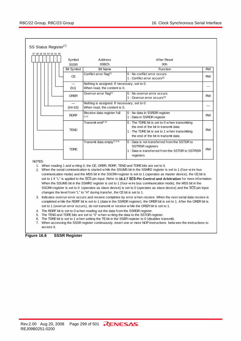
R8C/22 Group, R8C/23 Group 16. Clock Synchronous Serial Interface
Rev.2.00 Aug 20, 2008 Page 299 of 501REJ09B0251-0200
Figure 16.6 SSSR Register
SS Status Register(7)
Symbol Address After ResetSSSR 00BCh 00h
Bit Symbol Bit Name Function RW
NOTES:1.2.
3.
4.5.6.7.
Indicates overrun error occurs and receive completes by error w hen receive. When the next serial data receive iscompleted w hile the RDRF bit is set to 1 (data in the SSRDR register), the ORER bit is set to 1. After the ORER bit isset to 1 (overrun error occurs), do not transmit or receive w hile the ORER bit is set to 1.
When the serial communication is started w hile the SSUMS bit in the SSMR2 register is set to 1 (four-w ire buscommunication mode) and the MSS bit in the SSCRH register is set to 1 (operates as master device), the CE bit isset to 1 if “L” is applied to the SCS
_____ pin input. Refer to 16.2.7 SCS
_____Pin Control and Arbitration for more information.
changes the level from “L” to “H” during transfer, the CE bit is set to 1.SSCRH register is set to 0 (operates as slave device) is set to 0 (operates as slave device) and the SCS
_____ pin input
When the SSUMS bit in the SSMR2 register is set to 1 (four-w ire bus communication mode), the MSS bit in the
—
When accessing the SSSR register continuously, insert one or more NOP instructions betw een the instructions toaccess it.
The TEND and TDRE bits are set to “0” w hen w riting the data to the SSTDR register.
Overrun error f lag(1) 0 : No overrun error occurs1 : Overrun error occurs(3)
The TDRE bit is set to 1 w hen setting the TE bit in the SSER register to 0 (disables transmit).
TEND
Transmit end(1,5) 0 : The TDRE bit is set to 0 w hen transmitting the end of the bit in transmit data1 : The TDRE bit is set to 1 w hen transmitting the end of the bit in transmit data
RW
RW
ORER
—(b4-b3)
CE RW
RW
—
Conflict error f lag(1) 0 : No conflict error occurs1 : Conflict error occurs(2)
RDRFReceive data register full(1,4)
—(b1)
Nothing is assigned. If necessary, set to 0.When read, the content is 0.
0 : No data in SSRDR register1 : Data in SSRDR register
b3 b2 b1b7 b6 b5 b4 b0
When reading 1 and w riting 0, the CE, ORER, RDRF, TEND and TDRE bits are set to 0.
The RDRF bit is set to 0 w hen reading out the data from the SSRDR register.
Nothing is assigned. If necessary, set to 0.When read, the content is 0.
TDRE
Transmit data empty(1,5,6) 0 : Data is not transferred from the SSTDR to SSTRSR registers1 : Data is transferred from the SSTDR to SSTRSR registers
RW

R8C/22 Group, R8C/23 Group 16. Clock Synchronous Serial Interface
Rev.2.00 Aug 20, 2008 Page 300 of 501REJ09B0251-0200
Figure 16.7 SSMR2 Register
SS Mode Register 2
Symbol Address After ResetSSMR2 00BDh 00h
Bit Symbol Bit Name Function RW
SCS_____
pin open drain output select 0 : CMOS output1 : N-channel open drain output
SCS_____
pin select bit(2)b5 b4
0 0 : Functions as port0 1 : Function as SCS
_____ input pin
1 0 : Function as SCS_____
output pin(3)
1 1 : Functions as SCS_____
output pin(3)
NOTES:1.
2.
3.4.5.
The BIDE bit is disabled w hen the SSUMS bit is set to 0 (clock synchronous communication mode).
RWBIDE
Bidirectional mode enable bit(1,4) 0 : Standard mode (communicates using 2 pins of data input and data output)1 : Bidirectional mode (communicates using 1 pin of data input and data output)
This bit functions as the SCS_____
input pin before starting transfer.set to 0 (clock synchronous communication mode).
The SSI pin and SSO pin corresponding port direction bits are set to 0 (input mode) w hen the SOOS bit is set to 0(CMOS output).
RW
RW
RW
RW
RW
RW
0 : Clock synchronous communication mode1 : Four-w ire bus communication mode
SSCK pin open drain outputselect bit
0 : CMOS output1 : N-channel open drain output
CSS1
Clock synchronous serial I/O w ithchip select mode select bit(1)
SSO pin open drain output selectbit(1)
0 : CMOS output(5)
1 : N-channel open drain output
CSS0
SOOS
SCKOS
SSUMS
CSOS
b2 b1b7 b6 b5 b4 b0
Refer to 16.2.2.1 Association between Data I/O Pins and SS Shift Register for the combination of the data I/Opin.The SCS
______ pin functions as a port, regardless of the contents of the CSS0 and CSS1 bits w hen the SSUMS bit is
SCKSSSCK pin select bit 0 : Functions as port
1 : Functions as serial clock pin RW
b3

R8C/22 Group, R8C/23 Group 16. Clock Synchronous Serial Interface
Rev.2.00 Aug 20, 2008 Page 301 of 501REJ09B0251-0200
Figure 16.8 Registers SSTDR and SSRDR
Figure 16.9 PMR Register
SS Transmit Data Register
Symbol Address After ResetSSTDR 00BEh FFh
RW
RW
FunctionStore the transmit data.The stored transmit data is transferred to the SSTRSR register and the transmit is startedw hen detecting the SSTRSR register is empty.When the next transmit data is w ritten to the SSTDR register during the data transmit from theSSTRSR register, the data can be transmitted continuously.When the MLS bit in the SSMR register is set to 1 (transfer data w ith LSB-first), the data inw hich MSB and LSB are reversed can be read, after w riting to the SSTDR register.
b0b7
SS Receive Data Register
Symbol Address After ResetSSRDR 00BFh FFh
RW
NOTE:1. The SSRDR register maintains the receive data before the overrun error occurs w hen the ORER bit in the SSSR
register is set to 1 (overrun error occurs). When an overrun error occurs, the receive data may contain errors andtherefore, should be discarded.
Store the receive data.(1)
The receive data is transferred to the SSRDR register and the receive operation is completedw hen receiving 1-byte data to the SSTRSR register. At this time, the follow ing receive ispossible. The continuous receive is possible by the SSTRSR and SSRDR registers.
RO
Function
b0b7
Port Mode Register
Symbol Address After ResetPMR 00F8h 00h
Bit Symbol Bit Name Function RW
IICSEL RW0 : SSU function selects1 : I2C bus function selects
Set to 0
0 : I/O port P6_6, P6_71 : TXD1, RXD1Set to 0
—Reserved bits
SSU/I2C bus sw itch bit
RW
b0
0
—Reserved bits
U1PINSELPort TXD1/RXD1 sw itch bit
—(b3-b0)
—(b6-b5)
b3 b2
0b1
00b7 b6 b5 b4
0 0

R8C/22 Group, R8C/23 Group 16. Clock Synchronous Serial Interface
Rev.2.00 Aug 20, 2008 Page 302 of 501REJ09B0251-0200
16.2.1 Transfer ClockA transfer clock can be selected from 7 internal clocks (f1/256, f1/128, f1/64, f1/32, f1/16, f1/8 and f1/4) and anexternal clock. When using the clock synchronous serial I/O with chip select, set the SCKS bit in the SSMR2 register to 1 andselect the SSCK pin as the serial clock pin. When the MSS bit in the SSCRH register is set to 1 (operates as master device), an internal clock can beselected and the SSCK pin functions as output. When transfer is started, the SSCK pin outputs clocks of thetransfer rate selected in the CKS0 to CKS2 bits in the SSCRH register. When the MSS bit in the SSCRH register is set to 0 (operates as slave device), an external clock can be selectedand the SSCK pin functions as input.
16.2.1.1 Association between Transfer Clock Polarity, Phase, and DataAssociation between transfer clock polarity, phase and data changes according to a combination of the SSUMSbit in the SSMR2 register and the CPHS and CPOS bits in the SSMR register.Figure 16.10 shows the Association between Transfer Clock Polarity, Phase, and Transfer Data. Also, the MSB-first transfer or LSB-first transfer can be selected by setting the MLS bit in the SSMR register.When the MLS bit is set to 1, transfer is started from the LSB to MSB. When the MLS bit is set to 0, transfer isstarted from the MSB to LSB.

R8C/22 Group, R8C/23 Group 16. Clock Synchronous Serial Interface
Rev.2.00 Aug 20, 2008 Page 303 of 501REJ09B0251-0200
Figure 16.10 Association between Transfer Clock Polarity, Phase, and Transfer Data
SSCK
b0SSO, SSI
• When SSUMS bit = 0 (clock synchronous communication mode), CPHS bit = 0 (data change at oddedge) and CPOS bit = 0 (“H” when clock stops)
b1 b2 b3 b4 b5 b6 b7
SSCKCPOS = 0
(“H” when clock stops)
b0SSO, SSI
• When SSUMS bit = 1 (4-wire bus communication mode) and CPHS bit = 0 (data change at odd edge)
b1 b2 b3 b4 b5 b6 b7
SSCKCPOS = 1
(“L” when clock stops)
SCS
SSCKCPOS = 0
(“H” when clock stops)
SSO, SSI
• When SSUMS bit = 1 (4-wire bus communication mode), CPHS bit = 1 (data download at odd edge)
SSCKCPOS = 1
(“L” when clock stops)
SCS
b0 b1 b2 b3 b4 b5 b6 b7
CPHS and CPOS: bits in SSMR register, SSUMS: Bits in SSMR2 register

R8C/22 Group, R8C/23 Group 16. Clock Synchronous Serial Interface
Rev.2.00 Aug 20, 2008 Page 304 of 501REJ09B0251-0200
16.2.2 SS Shift Register (SSTRSR)The SSTRSR register is the shift register to transmit and receive the serial data. When the transmit data is transferred from the SSTDR register to the SSTRSR register and the MLS bit in theSSMR register is set to 0 (MSB-first), the bit 0 in the SSTDR register is transferred to the bit 0 in the SSTRSRregister. When the MLS bit is set to 1 (LSB-first), the bit 7 in the SSTDR register is transferred to the bit 0 in theSSTRSR register.
16.2.2.1 Association between Data I/O Pins and SS Shift RegisterConnecting association between the data I/O pin and SSTRSR register (SS shift register) changes according toa combination of the MSS bit in the SSCRH register and the SSUMS bit in the SSMR2 register. Also,connecting association changes according to the BIDE bit in the SSMR2 register.Figure 16.11 shows an Association between Data I/O Pins and SSTRSR Register.
Figure 16.11 Association between Data I/O Pins and SSTRSR Register
SSTRSR Register SSO
SSI
• When SSUMS bit = 0(clock synchronous communication mode)
SSTRSR Register SSO
SSI
• When SSUMS bit = 1 (4-wire bus communicationmode), BIDE bit = 0 (standard mode) and MSS bit = 0(operates as slave device)
SSTRSR Register SSO
SSI
• When SSUMS bit = 1 (4-wire bus communication mode),BIDE bit = 0 (standard mode) and MSS bit = 1 (operatesas master device)
SSTRSR Register SSO
SSI
• When SSUMS bit = 1 (4-wire bus communication mode),BIDE bit = 1 (bidirectional mode)
R8C/22 Group, R8C/23 Group 16. Clock Synchronous Serial Interface
Rev.2.00 Aug 20, 2008 Page 305 of 501REJ09B0251-0200
16.2.3 Interrupt RequestsClock synchronous serial I/O with chip select has five interrupt requests: transmit data empty, transmit end,receive data full, overrun error and conflict error. Since these interrupt requests are assigned to the clocksynchronous serial I/O with chip select interrupt vector table, determining interrupt sources by flags is required.Table 16.3 shows the Clock Synchronous Serial I/O with Chip Select Interrupt Requests.
CEIE, RIE, TEIE and TIE: Bits in SSER registerORER, RDRF, TEND and TDRE: Bits in SSSR register
Generation conditions of Table 16.3 are met, a clock synchronous serial I/O with chip select interrupt request isgenerated. Set the each interrupt source to 0 by a clock synchronous serial I/O with chip select interrupt routine.
However, the TDRE and TEND bits are automatically set to 0 by writing the transmit data to the SSTDRregister and the RDRF bit is automatically set to 0 by reading the SSRDR register. When writing the transmitdata to the SSTDR register, at the same time the TDRE bit is set to 1 (data is transmitted from the SSTDR toSSTRSR registers) again and when setting the TDRE bit to 0 (data is not transmitted from the SSTDR toSSTRSR registers), additional 1-byte data may be transmitted.
Table 16.3 Clock Synchronous Serial I/O with Chip Select Interrupt RequestsInterrupt Request Abbreviation Generation Condition
Transmit Data Empty TXI TIE = 1, TDRE = 1Transmit End TEI TEIE = 1, TEND = 1Receive Data Full RXI RIE = 1, RDRF = 1Overrun Error OEI RIE = 1, ORER = 1Conflict Error CEI CEIE = 1, CE = 1

R8C/22 Group, R8C/23 Group 16. Clock Synchronous Serial Interface
Rev.2.00 Aug 20, 2008 Page 306 of 501REJ09B0251-0200
16.2.4 Communication Modes and Pin FunctionsClock synchronous serial I/O with chip select switches functions of the I/O pin in each communication modeaccording to the setting of the MSS bit in the SSCRH register and the RE and TE bits in the SSER register.Table 16.4 shows the Association between Communication Modes and I/O Pins.
NOTES:1. This pin can be used as programmable I/O port.2. Do not set both the TE and RE bits to 1 in 4-wire bus (bidirectional) communication mode.
SSUMS and BIDE: Bits in SSMR2 registerMSS: Bit in SSCRH registerTE and RE: Bits in SSER register
Table 16.4 Association between Communication Modes and I/O Pins
Communication ModeBit Setting Pin State
SSUMS BIDE MSS TE RE SSI SSO SSCKClock Synchronous Communication Mode
0 Disabled 0 0 1 Input −(1) Input1 0 −(1) Output Input
1 Input Output Input1 0 1 Input −(1) Output
1 0 −(1) Output Output1 Input Output Output
4-Wire Bus Communication Mode
1 0 0 0 1 −(1) Input Input1 0 Output −(1) Input
1 Output Input Input1 0 1 Input −(1) Output
1 0 −(1) Output Output1 Input Output Output
4-Wire Bus (Bidirectional) Communication Mode(2)
1 1 0 0 1 −(1) Input Input1 0 −(1) Output Input
1 0 1 −(1) Input Output1 0 −(1) Output Output

R8C/22 Group, R8C/23 Group 16. Clock Synchronous Serial Interface
Rev.2.00 Aug 20, 2008 Page 307 of 501REJ09B0251-0200
16.2.5 Clock Synchronous Communication Mode
16.2.5.1 Initialization in Clock Synchronous Communication ModeFigure 16.12 shows an Initialization in Clock Synchronous Communication Mode. Set the TE bit in the SSERregister to 0 (disables transmit) and the RE bit to 0 (disables receive) before data transmit / receive as aninitialization.When communication mode and format are changed, set the TE bit to 0 and the RE bit to 0 before changing. Setting the RE bit to 0 does not change the contents of the RDRF and ORER flags, and the contents of theSSRDR register.
Figure 16.12 Initialization in Clock Synchronous Communication Mode
Start
SSMR2 register SSUMS bit ← 0
SSCRH register Set CKS0 to CKS2 bitsSet RSSTP bit
SSSR register ORER bit ← 0(1)
SSER register RE bit ← 1 (When receive)TE bit ← 1 (When transmit)Set RIE, TEIE and TIE bits
End
NOTE:1. Write 0 after reading 1 to set the ORER bit to 0.
SSER register RE bit ← 0TE bit ← 0
SSMR2 register SCKS bit ← 1Set SOOS bit
SSCRH register Set MSS bit
SSMR register CPHS bit ← 0CPOS bit ← 0Set MLS bit

R8C/22 Group, R8C/23 Group 16. Clock Synchronous Serial Interface
Rev.2.00 Aug 20, 2008 Page 308 of 501REJ09B0251-0200
16.2.5.2 Data TransmissionFigure 16.13 shows an Example of Clock Synchronous Serial I/O with Chip Select Operation for DataTransmission (Clock Synchronous Communication Mode). During the data transmit, the clock synchronousserial I/O with chip select operates as described below. When the clock synchronous serial I/O with chip select is set as a master device, it outputs a synchronous clockand data. When the clock synchronous serial I/O with chip select is set as a slave device, it outputs data synchronizedwith the input clock. When setting the TE bit to 1 (enables transmit) before writing the transmit data to theSSTDR register, the TDRE bit is automatically set to 0 (data is not transferred from the SSTDR to SSTRSRregisters) and the data is transferred from the SSTDR to SSTRSR registers.After the TDRE bit is set to 1 (data is transferred from the SSTDR to SSTRSR registers), a transmit is started.When the TIE bit in the SSER register is set to 1, the TXI interrupt request is generated. When one frame ofdata is transferred while the TDRE bit is set to 0, data is transferred from the SSTDR to SSTRSR registers anda transmit of the next frame is started. If the 8th bit is transmitted while the TDRE bit is set to 1, the TEND bitin the SSSR register is set to 1 (the TDRE bit is set to 1 when the last bit of the transmit data is transmitted) andthe state is retained. The TEI interrupt request is generated when the TEIE bit in the SSER register is set to 1(enables transmit-end interrupt request). The SSCK pin is retained “H” after transmit-end. Transmit can not be performed while the ORER bit in the SSSR register is set to 1 (overrun error occurs).Confirm that the ORER bit is set to 0 before transmit. Figure 16.14 shows a Sample Flowchart of Data Transmission (Clock Synchronous Communication Mode).
Figure 16.13 Example of Clock Synchronous Serial I/O with Chip Select Operation for Data Transmission (Clock Synchronous Communication Mode)
SSCK
b0SSO
• When SSUMS bit = 0 (clock synchronous communication mode), CPHS bit = 0 (data changeat odd numbers) and CPOS bit = 0 (“H” when clock stops)
b1 b7b0 b1b7
1 frame
TDRE bit inSSSR register 0
1
TEND bit inSSSR register 0
1
TEI interrupt requestgeneration
Write data to SSTDR registerProcess byprogram
1 frame
TXI interrupt request generation

R8C/22 Group, R8C/23 Group 16. Clock Synchronous Serial Interface
Rev.2.00 Aug 20, 2008 Page 309 of 501REJ09B0251-0200
Figure 16.14 Sample Flowchart of Data Transmission (Clock Synchronous Communication Mode)
Start
Initialization
Read TDRE bit in SSSR register
SSSR register TEND bit ← 0(1)
End
TDRE = 1 ?
Write transmit data to SSTDR register
Data transmitcontinued?
Read TEND bit in SSSR register
TEND = 1 ?
No
Yes
Yes
No
No
Yes
SSER register TE bit ← 0
(1)
(2)
(3)
(1) After reading the SSSR register and confirmingthat the TDRE bit is set to 1, write the transmitdata to the SSTDR register. When write thetransmit data to the SSTDR register, the TDRE bitis automatically set to 0.
(2) Determine whether data transmit is continued
(3) When the data transmit is completed, the TENDbit is set to 1. Set the TEND bit to 0 and the TE bitto 0 and complete transmit mode.
NOTE:1. Write 0 after reading 1 to set the TEND bit to 0.
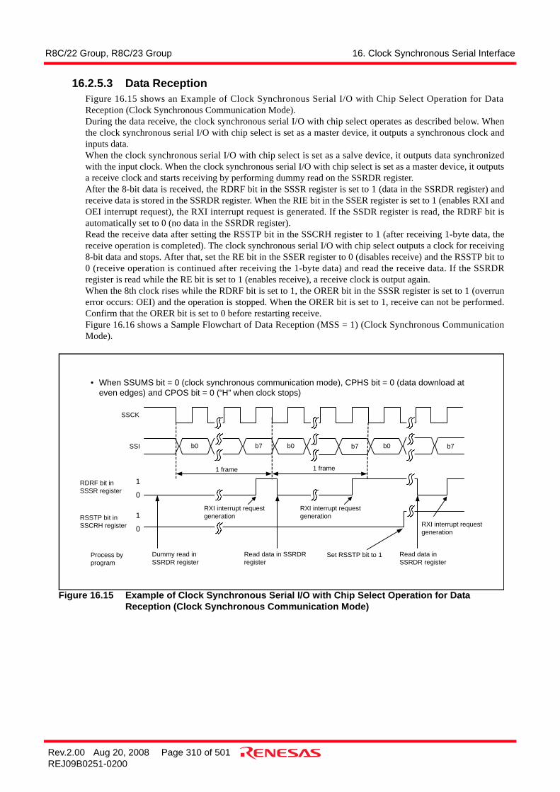
R8C/22 Group, R8C/23 Group 16. Clock Synchronous Serial Interface
Rev.2.00 Aug 20, 2008 Page 310 of 501REJ09B0251-0200
16.2.5.3 Data ReceptionFigure 16.15 shows an Example of Clock Synchronous Serial I/O with Chip Select Operation for DataReception (Clock Synchronous Communication Mode). During the data receive, the clock synchronous serial I/O with chip select operates as described below. Whenthe clock synchronous serial I/O with chip select is set as a master device, it outputs a synchronous clock andinputs data. When the clock synchronous serial I/O with chip select is set as a salve device, it outputs data synchronizedwith the input clock. When the clock synchronous serial I/O with chip select is set as a master device, it outputsa receive clock and starts receiving by performing dummy read on the SSRDR register. After the 8-bit data is received, the RDRF bit in the SSSR register is set to 1 (data in the SSRDR register) andreceive data is stored in the SSRDR register. When the RIE bit in the SSER register is set to 1 (enables RXI andOEI interrupt request), the RXI interrupt request is generated. If the SSDR register is read, the RDRF bit isautomatically set to 0 (no data in the SSRDR register).Read the receive data after setting the RSSTP bit in the SSCRH register to 1 (after receiving 1-byte data, thereceive operation is completed). The clock synchronous serial I/O with chip select outputs a clock for receiving8-bit data and stops. After that, set the RE bit in the SSER register to 0 (disables receive) and the RSSTP bit to0 (receive operation is continued after receiving the 1-byte data) and read the receive data. If the SSRDRregister is read while the RE bit is set to 1 (enables receive), a receive clock is output again. When the 8th clock rises while the RDRF bit is set to 1, the ORER bit in the SSSR register is set to 1 (overrunerror occurs: OEI) and the operation is stopped. When the ORER bit is set to 1, receive can not be performed.Confirm that the ORER bit is set to 0 before restarting receive. Figure 16.16 shows a Sample Flowchart of Data Reception (MSS = 1) (Clock Synchronous CommunicationMode).
Figure 16.15 Example of Clock Synchronous Serial I/O with Chip Select Operation for Data Reception (Clock Synchronous Communication Mode)
SSCK
b0SSI
• When SSUMS bit = 0 (clock synchronous communication mode), CPHS bit = 0 (data download ateven edges) and CPOS bit = 0 (“H” when clock stops)
b0b7
1 frame
RDRF bit inSSSR register 0
1
RSSTP bit inSSCRH register 0
1
Dummy read inSSRDR register
Process byprogram
RXI interrupt requestgeneration
b0b7 b7
1 frame
RXI interrupt requestgeneration
Read data in SSRDRregister
Read data inSSRDR register
Set RSSTP bit to 1
RXI interrupt requestgeneration

R8C/22 Group, R8C/23 Group 16. Clock Synchronous Serial Interface
Rev.2.00 Aug 20, 2008 Page 311 of 501REJ09B0251-0200
Figure 16.16 Sample Flowchart of Data Reception (MSS = 1) (Clock Synchronous Communication Mode)
Start
Initialization
Dummy read on SSRDR register
Read receive data in SSRDR register
Read ORER bit in SSSR register
Last datareceived?
Read RDRF bit in SSSR register
RDRF = 1 ?
No
Yes
Yes
No
No
Yes
(1)
(2)
(3)
(1) After setting each register in the clock synchronousserial I/O with chip select register, dummy read onthe SSRDR register is performed and receiveoperation is started.
(2) Determine whether the last 1-byte data is received.When the last 1-byte data is received, set to stopafter the data is received.
(3) When a receive error occurs, perform an error(6) process after reading the ORER bit. Then set the
ORER bit to 0. Transmit/receive can not berestarted while the ORER bit is set to 1.
(4) Confirm that the RDRF bit is set to 1. If the RDRFbit is set to 1, read the receive data in the SSRDRregister. If the SSRDR register is read, the RDRFbit is automatically set to 0.
ORER = 1 ?
End
Read receive data in SSRDR register
Read ORER bit in SSSR register
Read RDRF in SSSR register
RDRF = 1 ?No
YesORER = 1 ?
SSER register RE bit ← 0
SSCRH register RSSTP bit ← 0
SSCRH register RSSTP bit ← 1
Overrunerror
process
No
Yes
(4)
(5)
(6)
(7)
(7) Confirm that the RDRF bit is set to 1. When thereceive operation is completed, set the RSSTP bit to0 and the RE bit to 0 before reading the last 1-bytedata. If the SSRDR register is read before setting theRE bit to 0, the receive operation is restarted again.
(5)Before the last 1-byte data is received, set theRSSTP bit to 1 and stop after the data isreceived.

R8C/22 Group, R8C/23 Group 16. Clock Synchronous Serial Interface
Rev.2.00 Aug 20, 2008 Page 312 of 501REJ09B0251-0200
16.2.5.4 Data Transmission/ReceptionData transmit/receive is a combined operation of data transmit and receive which are described before.Transmit/receive is started by writing data in the SSTDR register. When the 8th clock rises or the ORER bit is set to 1 (overrun error occurs) while the TDRE bit is set to 1 (datais transferred from the SSTDR to SSTRSR registers), the transmit/receive operation is stopped. When switching from transmit mode (TE = 1) or receive mode (RE = 1) to transmit/receive mode (Te = RE =1),set the TE bit to 0 and RE bit to 0 before switching. After confirming that the TEND bit is set to 0 (the TDREbit is set to 0 when the last bit of the transmit data is transmitted), the RERF bit is set to 0 (no data in theSSRDR register) and the ORER bit is set to 0 (no overrun error), set the TE and RE bits to 1. Figure 16.17 shows a Sample Flowchart of Data Transmission/Reception (Clock Synchronous CommunicationMode).
When exiting transmit/receive mode after this mode is used (TE = RE = 1), a clock may be output if transmit/receive mode is exited after reading the SSRDR register. To avoid any clock outputs, perform either of thefollowing:• First set the RE bit to 0, and then set the TE bit to 0.• Set bits TE and RE at the same time.
When subsequently switching to receive mode (TE = 0 and RE = 1), first set the SRES bit to 1, and set this bitto 0 to reset the clock synchronous serial interface control unit and the SSTRSR register. Then, set the RE bit to1.

R8C/22 Group, R8C/23 Group 16. Clock Synchronous Serial Interface
Rev.2.00 Aug 20, 2008 Page 313 of 501REJ09B0251-0200
Figure 16.17 Sample Flowchart of Data Transmission/Reception (Clock Synchronous Communication Mode)
Start
Initialization
Read TDRE bit in SSSR register
SSSR register TEND bit ← 0(1)
End
TDRE=1 ?
Write transmit data to SSTDR register
Data transmitcontinued?
No
Yes
Yes
No
SSER register RE bit ← 0TE bit ← 0
(1)
(2)
(3)
(1) After reading the SSSR register and confirmingthat the TDRE bit is set to 1, write the transmitdata in the SSTDR register. When writing thetransmit data to the SSTDR register, the TDRE bitis automatically set to 0.
(5) Set the TEND bit to 0 and(6) the RE and TE bits in the SSER register to 0 before
ending transmit/receive mode.
Read receive data in SSRDR register
Read RDRF bit in SSSR register
RDRF=1 ?No
Yes
(4)
(2) Confirm that the RDRF bit is set to 1. If the RDRFbit is set to 1, read the receive data in the SSRDRregister. When reading the SSRDR register, theRDRF bit is automatically set to 0.
(3) Determine whether the transmit data is continued.
(5)
NOTE:1. Write 0 after reading 1 to set the TEND bit to 0.
Read TEND bit in SSSR register
TEND=1 ?
Yes
No
(6)
(4) When the data transmit is completed, the TENDbit in the SSSR register is set to 1.
R8C/22 Group, R8C/23 Group 16. Clock Synchronous Serial Interface
Rev.2.00 Aug 20, 2008 Page 314 of 501REJ09B0251-0200
16.2.6 Operation in 4-Wire Bus Communication Mode4-wire bus communication mode is a mode which communicates with the 4-wire bus; a clock line, data inputline, data output line and chip select line. This mode includes bidirectional mode in which the data input lineand data output line function as a single pin. The data input line and output line are changed according to the setting of the MSS bit in the SSCRH registerand the BIDE bit in the SSMR2 register. For details, refer to 16.2.2.1 Association between Data I/O Pins andSS Shift Register. In this mode, association between the clock polarity, phase and data can be set by the CPOSand CPHS bits in the SSMR register. For details, refer to 16.2.1.1 Association between Transfer ClockPolarity, Phase, and Data. When the clock synchronous serial I/O with chip select is set as a master device, the chip select line controlsoutput. When the clock synchronous serial I/O with chip select is set as a slave device, the chip select linecontrols input. When the clock synchronous serial I/O with chip select is set as master device, the chip selectline controls output of the SCS pin or controls output of a general port by setting the CSS1 bit in the SSMR2register. When the clock synchronous serial I/O with chip select is set as a slave device, the chip select line setthe SCS pin as an input pin by setting the CSS1 and CSS0 bits in the SSMR2 register to 01b. In 4-wire bus communication mode, the MLS bit in the SSMR register is set to 0 and communication isperformed using the MSB-first.
16.2.6.1 Initialization in 4-Wire Bus Communication ModeFigure 16.18 shows an Initialization in 4-Wire Bus Communication Mode. Before the data transit/receive, setthe TE bit in the SSER register to 0 (disables transmit) and the RE bit in the SSER register to 0 (disablesreceive) and initialize the clock synchronous serial I/O with chip select. When communication mode and format are changed, set the TE bit to 0 and the RE bit to 0 before changing. Setting the RE bit to 0 does not change the contents of the RDRF and ORER flags, and the contents of theSSRDR register.

R8C/22 Group, R8C/23 Group 16. Clock Synchronous Serial Interface
Rev.2.00 Aug 20, 2008 Page 315 of 501REJ09B0251-0200
Figure 16.18 Initialization in 4-Wire Bus Communication Mode
Start
SSMR2 register SSUMS bit ← 1
SSSR register ORER bit ← 0(1)
SSER register RE bit ← 1 (receive)TE bit ← 1 (transmit)Set bits RIE, TEIE, and TIE
End
SSER register RE bit ← 0TE bit ← 0
(2) Set the BIDE bit to 1 in bidirectional mode andset the I/O of the SCS pin by bits CSS0 andCSS1.
(1) (1) The MLS bit is set to 0 for MSB-first transfer.The clock polarity and phase are set by bitsCPHS and CPOS.
(2)
NOTE:1. Write 0 after reading 1 to set the ORER bit to 0.
SSMR2 register SCKS bit ← 1Set bits SOOS, CSS0 toCSS1, and BIDE
SSCRH register Set MSS bit
SSMR register Set bits CPHS and CPOSMLS bits ← 0
SSCRH register Set bits CKS0 to CKS2Set RSSTP bit

R8C/22 Group, R8C/23 Group 16. Clock Synchronous Serial Interface
Rev.2.00 Aug 20, 2008 Page 316 of 501REJ09B0251-0200
16.2.6.2 Data TransmissionFigure 16.19 shows an Example of Clock Synchronous Serial I/O with Chip Select Operation during DataTransmission (4-Wire Bus Communication Mode). During the data transmit, the clock synchronous serial I/Owith chip select operates as described below. When the clock synchronous serial I/O with chip select is set as a master device, it outputs a synchronous clockand data. When the UUSA is set as a slave device, it outputs data in synchronized with the input clock while“L” applies to the SCS pin. When writing the transmit data to the SSTDR register after setting the TE bit to 1 (enables transmit), the TDREbit is automatically set to 0 (data is not transferred from the SSTDR to SSTRSR registers) and the data istransferred from the SSTDR to SSTRSR registers. After the TDRE bit is set to 1 (data is transferred from theSSTDR to SSTRSR registers), a transmit is started. When the TIE bit in the SSER register is set to 1, the TXIinterrupt request is generated. When the 1-frame data is transferred while the TDRE bit is set to 0, the data is transferred from the SSTDR toSSTRSR registers and the next frame transmit is started. If the 8th bit is transmitted while the TDRE is set to 1,the TEND in the SSSR register is set to 1 (when the last bit of the transmit data is transmitted, the TDRE bit isset to 1) and the state is retained. If the TEIE bit in the SSER register is set to 1 (enables transmit-end interruptrequest), the TEI interrupt request is generated. The SSCK pin is retained “H” after transmit-end and the SCSpin is held “H”. When the SCS pin is transmitted When transmitting continuously while the SCS pin is held“L”, write the next transmit data to the SSTDR register before transmitting the 8th bit. Transmit can not be performed while the ORER bit in the SSSR register is set to 1 (overrun error occurs).Confirm that the ORER bit is set to 0 before transmit. The difference from the clock synchronous communication mode is that the SSO pin is placed in high-impedance state while the SCS pin is placed in high-impedance state when operating as a master device and theSSI pin is placed in high-impedance state while the SCS pin is placed in “H” input state when operating as aslave device. A sample flowchart is the same as the clock synchronous communication mode (refer to Figure 16.14 SampleFlowchart of Data Transmission (Clock Synchronous Communication Mode)).

R8C/22 Group, R8C/23 Group 16. Clock Synchronous Serial Interface
Rev.2.00 Aug 20, 2008 Page 317 of 501REJ09B0251-0200
Figure 16.19 Example of Clock Synchronous Serial I/O with Chip Select Operation during Data Transmission (4-Wire Bus Communication Mode)
TDRE bit inSSSR register 0
1
TEND bit inSSSR register 0
1
Data write to SSTDR registerProcess byprogram
SSCK
b0SSO
• When CPHS bit = 0 (data change at even edges), CPOS bit = 0 (“H” when clock stops)
b7
SCS(Output)
SSCK
• When CPHS bit = 1 (data change at even edges), CPOS bit = 0 (“H” when clock stops)
CPHS, CPOS: Bits in SSMR register
1 frame
TDRE bit inSSSR register 0
1
TEND bit inSSSR register 0
1
Data write to SSTDR registerProcess byprogram
1 frame
High-impedance
b0b7
High-impedanceSCS
(output)
TXI interrupt request isgenerated
b7 b0SSO
1 frame 1 frame
b6 b6
TXI interrupt request isgenerated
TEI interrupt request isgenerated
b6 b7 b0b6
TEI interrupt request isgenerated
TXI interrupt request isgenerated
TXI interrupt request isgenerated

R8C/22 Group, R8C/23 Group 16. Clock Synchronous Serial Interface
Rev.2.00 Aug 20, 2008 Page 318 of 501REJ09B0251-0200
16.2.6.3 Data ReceptionFigure 16.20 shows an Example of Clock Synchronous Serial I/O with Chip Select Operation during DataReception (4-Wire Bus Communication Mode). During the data receive, the clock synchronous serial I/O withchip select operates as described below. When the clock synchronous serial I/O with chip select is set as a master device, it outputs a synchronous clockand inputs data. When the clock synchronous serial I/O with chip select is set as a salve device, it outputs datasynchronized with the input clock while the SCS pin is held “L” input. When the clock synchronous serial I/Owith chip select is set as a master device, it outputs a receive clock and starts receiving by performing dummyread on the SSRDR register. After the 8-bit data is received, the RDRF bit in the SSSR register is set to 1 (data in the SSRDR register) andreceive data is stored in the SSRDR register. When the RIE bit in the SSER register is set to 1 (enables RXI andOEI interrupt request), the RXI interrupt request is generated. If the SSRDR register is read, the RDRF bit isautomatically set to 0 (no data in the SSRDR register).Read the receive data after setting the RSSTP bit in the SSCRH register to 1 (after receiving 1-byte data, thereceive operation is completed). The clock synchronous serial I/O with chip select outputs a clock for receiving8-bit data and stops. After that, set the RE bit in the SSER register to 0 (disables receive) and the RSSTP bit to0 (receive operation is continued after receiving 1-byte data) and read the receive data. If the SSRDR register isread while the RE bit is set to 1 (enables receive), a receive clock is output again. When the 8th clock rises while the RDRF bit is set to 1, the ORER bit in the SSSR register is set to 1 (overrunerror occurs: OEI) and the operation is stopped. When the ORER bit is set to 1, receive can not be performed.Confirm that the ORER bit is set to 0 before restarting receive. When the RDRF and ORER bits are set to 1, it varies depending on setting the CPHS bit in the SSMR register.Figure 16.20 shows when the RDRF and ORER bits are set to 1. When the CPHS bit is set to 1 (data download at the odd edges), the RDRF and ORER bits are set to 1 at onepoint of a frame.A sample flowchart is the same as the clock synchronous communication mode (refer to Figure 16.16 SampleFlowchart of Data Reception (MSS = 1) (Clock Synchronous Communication Mode)).

R8C/22 Group, R8C/23 Group 16. Clock Synchronous Serial Interface
Rev.2.00 Aug 20, 2008 Page 319 of 501REJ09B0251-0200
Figure 16.20 Example of Clock Synchronous Serial I/O with Chip Select Operation during Data Reception (4-Wire Bus Communication Mode)
SSCK
b0SSI
• When CPHS bit = 0 (data download at even edges) and CPOS bit = 0 (“H” when clock stops)
b7
SCS(Output)
SSCK
• When CPHS bit = 1 (data download at odd edges) and CPOS bit = 0 (“H” when clock stops)
CPHS and CPOS: Bit in SSMR register
1 frame
RDRF bit inSSSR register 0
1
RSSTP bit inSSCRH register 0
1
Dummy read inSSRDR register
Process byprogram
1 frame
High-impedance
b0b7
High-impedanceSCS
(Output)
b7 b0
Data read in SSRDRregister
RXI interrupt requestis generated
RXI interrupt requestis generated
Data read in SSRDRregister
RXI interrupt requestis generated
b0b7b0b7b7 b0SSI
1 frame
RDRF bit inSSSR register 0
1
RSSTP bit inSSCRH register 0
1
Dummy read inSSRDR register
Process byprogram
1 frame
Data read in SSRDRregister
RXI interrupt requestis generated
RXI interrupt requestis generated RXI interrupt request
is generated
Set RSSTPbit to 1
Data read in SSRDRregister
Set RSSTPbit to 1

R8C/22 Group, R8C/23 Group 16. Clock Synchronous Serial Interface
Rev.2.00 Aug 20, 2008 Page 320 of 501REJ09B0251-0200
16.2.7 SCS Pin Control and ArbitrationWhen setting the SSUMS bit in the SSMR2 register to 1 (4-wire bus communication mode), and the CSS1 bit inthe SSMR2 register to 1 (functions as SCS output pin), Set the MSS bit in the SSCRH register to 1 (operates asa master device) and check the arbitration of the SCS pin before starting serial transfer. If the clock synchronousserial I/O with chip select detects that the synchronized internal SCS signal is held “L” in this period, the CE bitin the SSSR register to 1 (a conflict error occurs) and the MSS bit is automatically set to 0 (operates as a slavedevice). Figure 16.21 shows an Arbitration Check Timing.
A future transmit operation is not performed while the CE bit is set to 1. Set the CE bit to 0 (a conflict error doesnot occur) before a transmit is started.
Figure 16.21 Arbitration Check Timing
Data write toSSTDR register
Maximum time of SCS internalsynchronization
During arbitration detection
High-impedance
SCS input
Internal SCS(synchronization)
MSS bit inSSCRH register
Transfer start
CE
SCS output
0
1

R8C/22 Group, R8C/23 Group 16. Clock Synchronous Serial Interface
Rev.2.00 Aug 20, 2008 Page 321 of 501REJ09B0251-0200
16.2.8 Notes on Clock Synchronous Serial I/O with Chip SelectSet the IICSEL bit in the PMR register to 0 (select clock synchronous serial I/O with chip select function) to usethe clock synchronous serial I/O with chip select.

R8C/22 Group, R8C/23 Group 16. Clock Synchronous Serial Interface
Rev.2.00 Aug 20, 2008 Page 322 of 501REJ09B0251-0200
16.3 I2C Bus InterfaceThe I2C bus interface is the circuit which is used for a serial communication based on the data transfer format of thePhilips I2C bus.Table 16.5 lists a I2C Bus Interface Specifications, Figure 16.22 shows a Block Diagram of I2C bus Interface andFigure 16.23 shows the External Circuit Connection Example of Pins SCL and SDA. Figures 16.24 to 16.31 showthe registers associated with the I2C bus interface.
* I2C bus is a trademark of Koninklijke Philips Electronics N. V.
NOTE:1. The interrupt sources can use the only I2C bus interface interrupt vector table.
Table 16.5 I2C Bus Interface SpecificationsItem Specification
Communication Formats
• I2C bus format- Selectable for master / slave device- Continuous transmit / receive (since the shift register, transmit data register
and receive data register are independent)- Start / stop conditions are automatically generated in master mode- Automatic loading of acknowledge bit when transmit- Bit synchronization / wait function (in master mode, the state of the SCL
signal is monitored per bit and the timing is synchronized automatically. If the transfer is not possible yet, stand by to set the SCL signal to “L”.
- Direct drive of the SCL and SDA pins (N-channel open drain output) is enabled
• Clock synchronous serial format- Continuous transmit / receive (since the shift register, transmit data register
and receive data register are independent)I/O Pins SCL (I/O): Serial clock I/O pin
SDA (I/O): Serial data I/O pinTransfer Clocks • When the MST bit in the ICCR1 register is set to 0
The external clock (input from the SCL pin) • When the MST bit in the ICCR1 register is set to 1
The internal clock selected by the CKS0 to CKS3 bits in the ICCR1 register (output from the SCL pin)
Receive Error Detection • Detects overrun error (clock synchronous serial format)An overrun error occurs during receive. When the last bit of the following data is received while the RDRF bit in the ICSR register is set to 1 (data in the ICDRR register), the AL bit is set to 1.
Interrupt Sources • I2C bus format .................................. 6 types(1)
Transmit data empty (including when slave address matches), transmit ends, receive data full (including when slave address matches), arbitration lost, NACK detection and stop condition detection.
• Clock synchronous serial format ...... 4 types(1)
Transmit data empty, transmit ends, receive data full and overrun errorSelect Functions • I2C bus format
- Selectable for the output level of the acknowledge signal when receive• Clock synchronous serial format
- Selectable for the MSB-first or LSB-first to the data transfer direction

R8C/22 Group, R8C/23 Group 16. Clock Synchronous Serial Interface
Rev.2.00 Aug 20, 2008 Page 323 of 501REJ09B0251-0200
Figure 16.22 Block Diagram of I2C Bus Interface
ICCR1 register
Dat
a bu
s
ICCR2 register
ICMR register
ICDRT register
SAR register
ICSR register
Address comparisoncircuit
OutputcontrolSCL
Interrupt request(TXI, TEI, RXI, STPI, NAKI)
Transfer clockgeneration
circuit
ICDRS register
ICDRR register
Bus state judgmentcircuit
Arbitration judgmentcircuit
ICIER register
Interrupt generationcircuit
Transmit / receivecontrol circuit
Noiserejection
circuit
SDA Outputcontrol
f1
Noiserejection
circuit
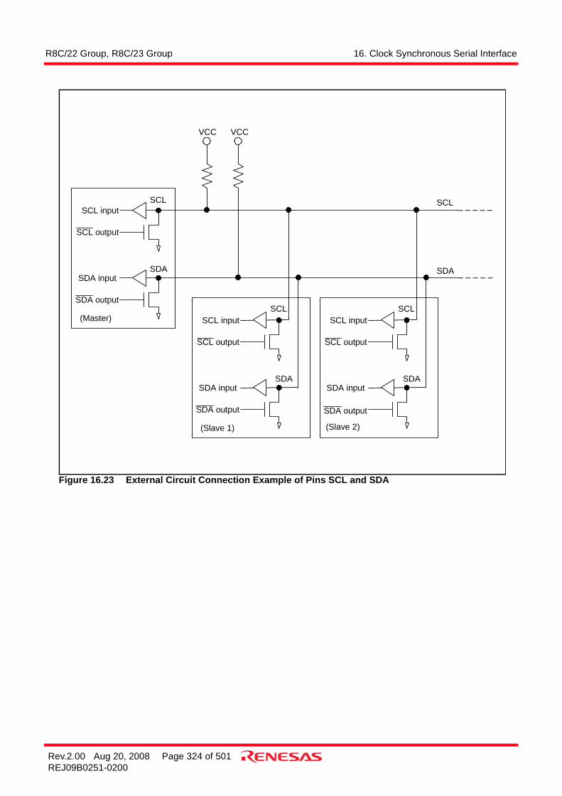
R8C/22 Group, R8C/23 Group 16. Clock Synchronous Serial Interface
Rev.2.00 Aug 20, 2008 Page 324 of 501REJ09B0251-0200
Figure 16.23 External Circuit Connection Example of Pins SCL and SDA
SCL
SDA
SCL input
SCL output
SDA input
SDA output
(Master)
VCC VCC
SCL
SDA
SCL input
SCL output
SDA input
SDA output
(Slave 1)
SCL
SDA
SCL input
SCL output
SDA input
SDA output
SCL
SDA
(Slave 2)

R8C/22 Group, R8C/23 Group 16. Clock Synchronous Serial Interface
Rev.2.00 Aug 20, 2008 Page 325 of 501REJ09B0251-0200
Figure 16.24 ICCR1 Register
IIC Bus Control Register 1
Symbol Address After ResetICCR1 00B8h 00h
Bit Symbol Bit Name Function RW
NOTES:1.
2.3.
4.
5.
6.
Master / slave select bit(5,6)
In master mode w ith the I2C bus format, w hen arbitration is lost, the MST and TRS bits are set to 0 and the IIC entersslave receive mode.When an overrun error occurs in master receive mode of the clock synchronous serial format, the MST bit is set to 0and the IIC enters slave receive mode.
b0
Rew rite the TRS bit betw een the transfer frame.
RCVD
Receive disable bit After reading the ICDRR register w hile the TRS bitis set to 00 : Maintains the follow ing receive operation1 : Disables the follow ing receive operation
RW
b3 b2
RW
RW
b1b7 b6 b5 b4
CKS2
CKS3
CKS0
CKS1
RW
TRS
Transmit clock select bit 3 to0(1)
b3 b2 b1 b0
0 0 0 0 : f1/280 0 0 1 : f1/400 0 1 0 : f1/480 0 1 1 : f1/640 1 0 0 : f1/800 1 0 1 : f1/1000 1 1 0 : f1/1120 1 1 1 : f1/1281 0 0 0 : f1/561 0 0 1 : f1/801 0 1 0 : f1/961 0 1 1 : f1/1281 1 0 0 : f1/1601 1 0 1 : f1/2001 1 1 0 : f1/2241 1 1 1 : f1/256
b5 b4
0 0 : Slave receive mode(4)
0 1 : Slave transmit mode1 0 : Master receive mode1 1 : Master transmit mode
RW
MST RW
RWTransfer / receive selectbit(2,3,6)
In multimaster operation use the MOV instruction to set bits TRS and MST.
When the f irst 7 bits, after the start condition in slave receive mode, match w ith the slave address set in the SARregister and the 8th bit is set to 1, the TRS bit is set to 1.
RWICE
I2C bus interface enable bit 0 : This module is halted (SCL and SDA pins are set to port function)1 : This module is enabled for transfer operations (SCL and SDA pins are bus drive state)
Set according to the necessary transfer rate in master mode. Refer to Table 16.6 Transfer Rate Examples for thetransfer rate. This bit is used for maintaining of the setup time in transmit mode. The time is 10Tcyc w hen the CKS3bit is set to 0 and 20Tcyc w hen the CKS3 bit is set to 1. (1Tcyc = 1/f1(s))

R8C/22 Group, R8C/23 Group 16. Clock Synchronous Serial Interface
Rev.2.00 Aug 20, 2008 Page 326 of 501REJ09B0251-0200
Figure 16.25 ICCR2 Register
IIC Bus Control Register 2
Symbol Address After ResetICCR2 00B9h 01111101b
Bit Symbol Bit Name Function RW
NOTES:1.2.3.
4.
—(b0)
Nothing is assigned. If necessary, set to 0.When read, the content is 1. —
IICRST RW
RO
RW
—
IIC control part reset bit
b0b3 b2 b1b7 b6 b5 b4
When hang-up occurs due to communication failureduring I2C bus interface operation and w rite 1, resetcontrol part of I2C bus interface w ithout setting portand initializing register.
—(b2)
Nothing is assigned. If necessary, set to 0.When read, the content is 1.
SCLOSCL monitor f lag 0 : SCL pin is set to “L”
1 : SCL pin is set to “H”
SDAOP
SDAO RW
When read0 : SDA pin output is held “L”1 : SDA pin output is held “H”When w rite(1,2)
0 : SDA pin output is changed to “L”1 : SDA pin output is changed to high-impedance (“H” output is external pull-up resistor)
SDA output value controlbit
SDAO w rite protect bit When rew rite to SDAO bit, w rite 0 simultaneously.(1)
When read, its content is 1.
When read0 : Bus is in released state (SDA signal changes from “L” to “H” w hile SCL signal is in “H” state)1 : Bus is in occupied state (SDA signal changes from “H” to “L” w hile SCL signal is in “H” state)When w rite(3)
0 : Generates stop condition1 : Generates start condition
RW
This bit is disabled w hen the clock synchronous serial format is used.
This bit is enabled in master mode. When w rite to the BBSY bit, w rite 0 to the SCP bit using the MOV instructionsimultaneously. Execute the same w ay w hen the start condition is regenerating.
When w riting to the SDAO bit, w rite 0 to the SDAOP bit using the MOV instruction simultaneously.Do not w rite during transfer operation.
BBSY
Bus busy bit(4)
SCPStart / stop conditiongeneration disable bit
When w rite to BBSY bit, w rite 0 simultaneously.(3)
When read, its content is 1.Writing 1 is disabled.
RW

R8C/22 Group, R8C/23 Group 16. Clock Synchronous Serial Interface
Rev.2.00 Aug 20, 2008 Page 327 of 501REJ09B0251-0200
Figure 16.26 ICMR Register
IIC Bus Mode Register
Symbol Address After ResetICMR 00BAh 00011000b
Bit Symbol Bit Name Function RW
MSB-first / LSB-first select
NOTES:1.2.3.
4.5.
6.
MLS RW
RW
BC1
BC2
Bit counter 2 to 0 I2C bus format (remaining transfer bit numbersw hen read out and data bit numbers of transfer tothe next w hen w rite)(1,2)
b2 b1 b0
0 0 0 : 9 bits(3)
0 0 1 : 2 bits0 1 0 : 3 bits0 1 1 : 4 bits1 0 0 : 5 bits1 0 1 : 6 bits1 1 0 : 7 bits1 1 1 : 8 bitsClock synchronous serial format (w hen read, readthe remaining transfer bit numbers and w hen w rite,w rite 000b.)b2 b1 b0
0 0 0 : 8 bits0 0 1 : 1 bit0 1 0 : 2 bits0 1 1 : 3 bits1 0 0 : 4 bits1 0 1 : 5 bits1 1 0 : 6 bits1 1 1 : 7 bits
BC0
RW
RW
0
Wait insertion bit(5)
BCWPBC w rite protect bit
b7 b6 b5 b4 b3 b2 b1 b0
When rew rite to the BC0 to BC2 bits, w rite 0simultaneously.(2,4)
When read, its content is 1.RW
The setting value is enabled in master mode of the I2C bus format. It is disabled in slave mode of the I2C bus format orw hen the clock synchronous serial format is used.
0 : No w ait (Transfer data and acknow ledge bit consecutively)1 : Wait (After the falling of the clock for the f inal data bit, “L” period is extended for tw o transfer clocks)
Set to 0RW
RW
0 : Data transfer by MSB-first(6)
1 : Data transfer by LSB-first
—(b5)
WAIT
Set to 0 w hen the I2C bus format is used.
When w rite to the BC0 to BC2 bits, w rite 0 to the BCWP bit using the MOV instruction.
—(b4)
Nothing is assigned. If necessary, set to 0.When read, the content is 1. —
Rew rite betw een transfer frames. When w rite values other than 000b, w rite w hen the SCL signal is “L”.
After data including the acknow ledge bit is transferred, bits b2 to b0 are automatically set to 000b. When the startcondition is detected, these bits are automatically set to 000b.Do not rew rite w hen the clock synchronous serial format is used.
Reserved bit

R8C/22 Group, R8C/23 Group 16. Clock Synchronous Serial Interface
Rev.2.00 Aug 20, 2008 Page 328 of 501REJ09B0251-0200
Figure 16.27 ICIER Register
IIC Bus Interrupt Enable Register
Symbol Address After ResetICIER 00BBh 00h
Bit Symbol Bit Name Function RW
NOTES:1.2.
Transmit acknow ledgeselect bit
0 : 0 is transmitted as acknow ledge bit in receive mode1 : 1 is transmitted as acknow ledge bit in receive mode
b0b3 b2 b1
NAKIE
b7 b6 b5 b4
ACKE
Transmit end interruptenable bit
STIE
ACKBT RW
RW
ROACKBR
RW
Receive acknow ledge bit 0 : Acknow ledge bit w hich is received from receive device in transmit mode is set to 01 : Acknow ledge bit w hich is received from receive device in transmit mode is set to 1
RW
An overrun error interrupt request is generated w hen the clock synchronous format is used.
RIE
Receive interrupt enablebit
0 : Disables receive data full and overrun error interrupt request1 : Enables receive data full and overrun error interrupt request(1)
RW
TIETransmit interrupt enablebit
0 : Disables transmit data empty interrupt request1 : Enables transmit data empty interrupt request
TEIE
Set the STIE bit to 1 (enable stop condition detection interrupt request) w hen the STOP bit in the ICSR register is setto 0.
0 : Disables transmit end interrupt request1 : Enables transmit end interrupt request
RW
Acknow ledge bit judgmentselect bit
0 : Value of receive acknow ledge bit is ignored and continuous transfer is performed1 : When receive acknow ledge bit is set to 1, continuous transfer is halted
RW
Stop condition detectioninterrupt enable bit
0 : Disables stop condition detection interrupt request1 : Enables stop condition detection interrupt request(2)
0 : Disables NACK receive interrupt request and arbitration lost / overrun error interrupt request1 : Enables NACK receive interrupt request and arbitration lost / overrun error interrupt request(1)
NACK receive interruptenable bit

R8C/22 Group, R8C/23 Group 16. Clock Synchronous Serial Interface
Rev.2.00 Aug 20, 2008 Page 329 of 501REJ09B0251-0200
Figure 16.28 ICSR Register
IIC Bus Status Register(7)
Symbol Address After ResetICSR 00BCh 0000X000b
Bit Symbol Bit Name Function RW
NOTES:1.2.3.
4.
5.6.7.
RW
STOPStop condition detectionflag(1)
When the stop condition is detected after the frameis transferred, this f lag is set to 1 RW
RDRFReceive data register full(1,5)
TEND
Transmit end(1,6)
The RDRF bit is set to 0 when reading data f rom the ICDRR register.The TEND and TDRE bits are set to 0 when writing data to the ICDRT register.
When two or more master dev ices attempt to occupy the bus at nearly the same time, if the I2C bus Interf ace monitors the SDA pinand the data which the IIC transmits is dif f erent, the AL f lag is set to 1 and the bus is occupied by the other masters.
This f lag is set to 1 w hen the first frame follow ingstart condition matches the SVA0 to SVA6 bits inthe SAR register in slave receive mode. (Detect theslave address and generate call address)
RW
No acknow ledge detectionflag(1,4)
This f lag is enabled in slav e receiv e mode of the I2C bus f ormat.Each bit is set to 0 when reading 1 bef ore writing 0.
NACKFWhen no acknow ledge is detected from receivedevice w hen transmit, this f lag is set to 1 RW
RW
When receive data is transferred from ICDRS toICDRR registers, this f lag is set to 1
AL
ADZ
When the 9th clock of the SCL signal w ith the I2Cbus format w hile the TDRE bit is set to 1, this f lag isset to 1This f lag is set to 1 w hen the final bit of thetransmit frame is transmitted w ith the clocksynchronous format
RW
RW
General call addressrecognition flag(1,2)
When detecting the general call address, this f lagis set to 1.
Arbitration lost f lag /overrun error f lag(1)
When the I2C bus format is used, this f lag indicatesthat arbitration is lost in master mode. In thefollow ing case, this f lag is set to 1.(3)
• When the internal SDA signal and SDA pin level do not match at the rise of the SCL signal in master transmit mode• When the start condition is detected and the SDA pin is held “H” in master transmit / receive mode
This f lag indicates that an overrun error occursw hen the clock synchronous format is usedIn the follow ing case, this f lag is set to 1.• When the last bit of the follow ing data is received w hile the RDRF bit is set to 1
Slave address recognitionflag(1)
AAS
b3 b2 b1b7 b6 b5 b4
When accessing the ICSR register continuously , insert one or more NOP instructions between the instructions to access it.
b0
The NACKF bit is enabled when the ACKE bit in the ICIER register is set to 1 (when the receiv e acknowledge bit is set to 1, transf er ishalted)
TDRE
Transmit data empty(1,6) In the follow ing cases, this f lag is set to 1• Data is transferred from ICDRT to ICDRS registers and ICDRT register is empty• When setting the TRS bit in the ICCR1 register to 1 (transmit mode)• When generating the start condition (including retransmit)• When changing from slave receive mode to slave transmit mode
RW

R8C/22 Group, R8C/23 Group 16. Clock Synchronous Serial Interface
Rev.2.00 Aug 20, 2008 Page 330 of 501REJ09B0251-0200
Figure 16.29 Registers SAR and ICDRT
Slave Address Register
Symbol Address After ResetSAR 00BDh 00h
Bit Symbol Bit Name Function RW
RWSVA3
SVA6SVA5SVA4
RW
RW
Slave address 6 to 0 Set the different address from the other slavedevices w hich are connected to the I2C bus.When the 7 high-order bits of the f irst frametransmitted after the starting condition matchthe SVA0 to SVA6 bits in slave mode of the I2Cbus format, the MCU operates as a slavedevice.
RW
RW
RW
RW
FSFormat select bit 0 : I2C bus format
1 : Clock synchronous serial format RW
SVA2
SVA0SVA1
b7 b6 b0b1b5 b3 b2b4
IIC Bus Transmit Data Register
Symbol Address After ResetICDRT 00BEh FFh
RW
RW
FunctionStore transmit dataWhen detecting that the ICDRS register is empty, the stored transmit data is transferred to theICDRS register and the starts transmit data.When the next transmit data is w ritten to the ICDRT register during transmitting the data of theICDRS register, continuous transmit is enabled. When the MLS bit in the ICMR register is set to1 (data transferred by LSB-first) and after the data is w ritten to the ICDRT register, the MSBand LSB inverted data is read.
b0b7

R8C/22 Group, R8C/23 Group 16. Clock Synchronous Serial Interface
Rev.2.00 Aug 20, 2008 Page 331 of 501REJ09B0251-0200
Figure 16.30 Registers ICDRR and ICDRS
Figure 16.31 PMR Register
IIC Bus Receive Data Register
Symbol Address After ResetICDRR 00BFh FFh
RW
b7 b0
Store receive dataWhen the ICDRS register receives 1-byte data, the receive data is transferred to the ICDRRregister and the next receive is enabled.
RO
Function
IIC Bus Shift Register
SymbolICDRS
RW
b7 b0
This register is a register that is used to transmit and receive data.The transmit data is transferred from the ICDRT to ICDRS registers and data is transmittedfrom the SDA pin w hen transmitting.When 1-byte data is received, data is transferred from the ICDRS to ICDRR registers w henreceiving.
—
Function
Port Mode Register
Symbol Address After ResetPMR 00F8h 00h
Bit Symbol Bit Name Function RW
IICSEL RW0 : SSU function selects1 : I2C bus function selects
Set to 0
0 : I/O port P6_6, P6_71 : TXD1, RXD1Set to 0
—Reserved bits
SSU/I2C bus sw itch bit
RW
b0
0
—Reserved bits
U1PINSELPort TXD1/RXD1 sw itch bit
—(b3-b0)
—(b6-b5)
b3 b2
0b1
00b7 b6 b5 b4
0 0
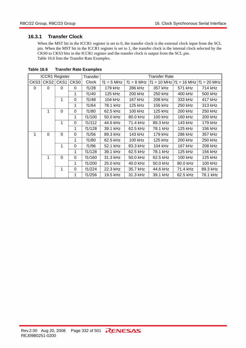
R8C/22 Group, R8C/23 Group 16. Clock Synchronous Serial Interface
Rev.2.00 Aug 20, 2008 Page 332 of 501REJ09B0251-0200
16.3.1 Transfer ClockWhen the MST bit in the ICCR1 register is set to 0, the transfer clock is the external clock input from the SCLpin. When the MST bit in the ICCR1 register is set to 1, the transfer clock is the internal clock selected by theCKS0 to CKS3 bits in the ICCR1 register and the transfer clock is output from the SCL pin.Table 16.6 lists the Transfer Rate Examples.
Table 16.6 Transfer Rate ExamplesICCR1 Register Transfer
ClockTransfer Rate
CKS3 CKS2 CKS1 CKS0 f1 = 5 MHz f1 = 8 MHz f1 = 10 MHz f1 = 16 MHz f1 = 20 MHz0 0 0 0 f1/28 179 kHz 286 kHz 357 kHz 571 kHz 714 kHz
1 f1/40 125 kHz 200 kHz 250 kHz 400 kHz 500 kHz1 0 f1/48 104 kHz 167 kHz 208 kHz 333 kHz 417 kHz
1 f1/64 78.1 kHz 125 kHz 156 kHz 250 kHz 313 kHz1 0 0 f1/80 62.5 kHz 100 kHz 125 kHz 200 kHz 250 kHz
1 f1/100 50.0 kHz 80.0 kHz 100 kHz 160 kHz 200 kHz1 0 f1/112 44.6 kHz 71.4 kHz 89.3 kHz 143 kHz 179 kHz
1 f1/128 39.1 kHz 62.5 kHz 78.1 kHz 125 kHz 156 kHz1 0 0 0 f1/56 89.3 kHz 143 kHz 179 kHz 286 kHz 357 kHz
1 f1/80 62.5 kHz 100 kHz 125 kHz 200 kHz 250 kHz1 0 f1/96 52.1 kHz 83.3 kHz 104 kHz 167 kHz 208 kHz
1 f1/128 39.1 kHz 62.5 kHz 78.1 kHz 125 kHz 156 kHz1 0 0 f1/160 31.3 kHz 50.0 kHz 62.5 kHz 100 kHz 125 kHz
1 f1/200 25.0 kHz 40.0 kHz 50.0 kHz 80.0 kHz 100 kHz1 0 f1/224 22.3 kHz 35.7 kHz 44.6 kHz 71.4 kHz 89.3 kHz
1 f1/256 19.5 kHz 31.3 kHz 39.1 kHz 62.5 kHz 78.1 kHz

R8C/22 Group, R8C/23 Group 16. Clock Synchronous Serial Interface
Rev.2.00 Aug 20, 2008 Page 333 of 501REJ09B0251-0200
16.3.2 Interrupt RequestsThe interrupt request of the I2C bus interface contains 6 types when the I2C bus format is used and 4 types whenthe clock synchronous serial format is used.Table 16.7 lists the Interrupt Requests of I2C Bus Interface.Since these interrupt requests are allocated at the I2C bus interface interrupt vector table, determining the sourceby each bit is necessary.
STIE, NAKIE, RIE, TEIE, TIE: Bits in ICIER registerAL, STOP, NACKF, RDRF, TEND, TDRE: Bits in ICSR register
When the generation conditions on the Table 16.7 are met, the I2C bus interface interrupt request is generated.Set the interrupt generation conditions to 0 by the I2C bus interface interrupt routine. However, the TDRE andTEND bits are automatically set to 0 by writing transmit data to the ICDRT register and the RDRF bit isautomatically set to 0 by reading the ICDRR register. When writing transmit data to the ICDRT register, theTDRE bit is set to 0. When data is transferred from the ICDRT to ICDRS registers, the TDRE bit is set to 1 andwhen further setting the TDRE bit to 0, extra 1 byte may be transmitted.Also, set the STIE bit to 1 (enable stop condition detection interrupt request) when the STOP bit is set to 0.
Table 16.7 Interrupt Requests of I2C Bus Interface
Interrupt Request Generation Condition
Format
I2C busClock
Synchronous Serial
Transmit Data Empty TXI TIE = 1 and TDRE = 1 Enabled EnabledTransmit Ends TEI TEIE = 1 and TEND = 1 Enabled EnabledReceive Data Full RXI RIE = 1 and RDRF = 1 Enabled EnabledStop Condition Detection STPI STIE = 1 and STOP = 1 Enabled DisabledNACK Detection NAKI NAKIE = 1 and AL = 1 (or
NAKIE = 1 and NACKF = 1)Enabled Disabled
Arbitration Lost / Overrun Error Enabled Enabled

R8C/22 Group, R8C/23 Group 16. Clock Synchronous Serial Interface
Rev.2.00 Aug 20, 2008 Page 334 of 501REJ09B0251-0200
16.3.3 I2C Bus Interface Mode
16.3.3.1 I2C Bus FormatSetting the FS bit in the SAR register to 0 communicates in I2C bus format.Figure 16.32 shows the I2C Bus Format and Bus Timing. The 1st frame following start condition consists of 8bits.
Figure 16.32 I2C Bus Format and Bus Timing
SDA
SCL
S SLA R/W A DATA A DATA A P
1 to 7 8 9 1 to 7 8 9 1 to 7 8 9
(2) I2C bus timing
Explanation of symbolsS : Start condition The master device changes the SDA signal from “H” to “L” while the SCL signal is held “H”.SLA : Slave addressR/W : Indicates the direction of data transmit/receive Data is transmitted from the slave device to the master device when R/W value is 1 and from the master device to the slave device when
R/W value is 0.A : Acknowledge The receive device sets the SDA signal to “L”.DATA : Transmit / receive dataP : Stop condition The master device changes the SDA signal from “L” to “H” while the SCL signal is held “H”.
S R/W A DATA A A/A P
1 7 1 1 n 1 1 1
1 m
(a) I2C bus format (FS = 0)
Transfer bit numbers (n = 1 to 8)
Transfer frame numbers (m = from 1)
S R/W A DATA A/A P
1 7 1 1 n1 1 1
1 m1
(b) I2C bus format (when start condition is retransmitted, FS = 0)
Upper: Transfer bit numbers (n1, n2 = 1 to 8)Lower: Transfer frame numbers (m1, m2 = from 1 )
SLA
SLA A/A
1
S
1
R/W A DATA
7 1 1 n2
SLA
1 m2
(1) I2C bus Format

R8C/22 Group, R8C/23 Group 16. Clock Synchronous Serial Interface
Rev.2.00 Aug 20, 2008 Page 335 of 501REJ09B0251-0200
16.3.3.2 Master Transmit OperationIn master transmit mode, the master device outputs the transmit clock and data, and the slave device returns anacknowledge signal.Figure 16.33 and Figure 16.34 show the Operation Timing in Master Transmit Mode (I2C Bus Interface Mode).
The transmit procedure and operation in master transmit mode are shown below.(1) Set the STOP bit in the ICSR register to 0 to reset it. And then set the ICE bit in the ICCR1 register to 1
(transfer operation enabled). Set the WAIT and MLS bits in the ICMR register and set the CKS0 toCKS3 bits in the ICCR1 register (initial setting).
(2) Read the BBSY bit in the ICCR2 register to confirm that the bus is free. Set the TRS and MST bits inthe ICCR1 register to master transmit mode. The start condition is generated by writing 1 to the BBSYbit and 0 to the SCP bit by the MOV instruction.
(3) After confirming that the TDRE bit in the ICSR register is set to 1 (data is transferred from the ICDRTto ICDRS registers), write transmit data to the ICDRT register (data in which a slave address and R/Ware shown at the 1st byte). At this time, the TDRE bit is automatically set to 0 and data is transferredfrom the ICDRT to ICDRS registers, the TDRE bit is set to 1 again.
(4) When the transmit of 1-byte data is completed while the TDRE bit is set to 1, the TEND bit in the ICSRregister is set to 1 at the rise of the 9th transmit clock pulse. Read the ACKBR bit in the ICIER register,and confirm that the slave is selected. Write the 2nd-byte data to the ICDRT register. Since the slavedevice is not acknowledged when the ACKBR bit is set to 1, generate the stop condition. The stopcondition is generated by the writing 0 to the BBSY bit and 0 to the SCP bit by the MOV instruction.The SCL signal is held “L” until data is available and the stop condition is generated.
(5) Write the transmit data after the 2nd byte to the ICDRT register every time the TDRE bit is set to 1.(6) When writing the number of bytes to be transmitted to the ICDRT register, wait until the TEND bit is
set to 1 while the TDRE bit is set to 1. Or wait for NACK (the NACKF bit in the ICSR register is set to1) from the receive device while the ACKE bit in the ICIER register is set to 1 (when the receiveacknowledge bit is set to 1, transfer is halted). And generate the stop condition before setting the TENDand NACKF bits to 0.
(7) When the STOP bit in the ICSR register is set to 1, return to slave receive mode.

R8C/22 Group, R8C/23 Group 16. Clock Synchronous Serial Interface
Rev.2.00 Aug 20, 2008 Page 336 of 501REJ09B0251-0200
Figure 16.33 Operating Timing in Master Transmit Mode (I2C Bus Interface Mode) (1)
Figure 16.34 Operating Timing in Master Transmit Mode (I2C Bus Interface Mode) (2)
SDA(master output)
SCL(master output) 1 2 8 96 74 53
b7 b6 b5 b4 b3 b2 b1 b0 b7 b6
1 2
SDA(slave output)
TDRE bit inICSR register
1
0
TEND bit inICSR register
1
0
ICDRT register
ICDRS register
R/WSlave address
Address + R/W
Processingby program
(2) Instruction ofstart conditiongeneration
(3) Data write to ICDRTregister (1st byte)
A
(4) Data write to ICDRTregister (2nd byte)
(5) Data write to ICDRTregister (3rd byte)
Data 2
Address + R/W
Data 1
Data 1
SDA(master output)
SCL(master output) 1 2 8 96 74 53
b7 b6 b5 b4 b3 b2 b1 b0
SDA(slave output)
TDRE bit inICSR register
1
0
TEND bit inICSR register
1
0
ICDRT register
ICDRS register
Data n
Processingby program
(6) Generate stop condition andset TEND bit to 0
(3) Data write to ICDRTregister
A/A
(7) Set to slave receive mode
9
A
Data n
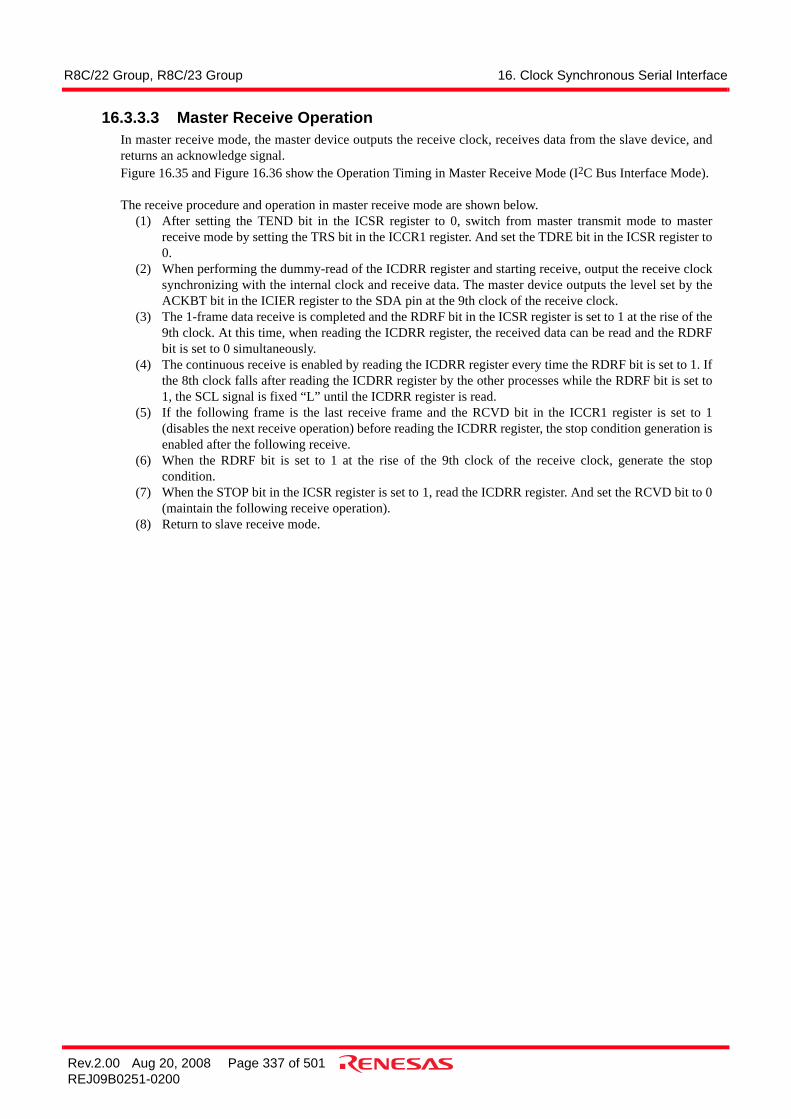
R8C/22 Group, R8C/23 Group 16. Clock Synchronous Serial Interface
Rev.2.00 Aug 20, 2008 Page 337 of 501REJ09B0251-0200
16.3.3.3 Master Receive OperationIn master receive mode, the master device outputs the receive clock, receives data from the slave device, andreturns an acknowledge signal.Figure 16.35 and Figure 16.36 show the Operation Timing in Master Receive Mode (I2C Bus Interface Mode). The receive procedure and operation in master receive mode are shown below.
(1) After setting the TEND bit in the ICSR register to 0, switch from master transmit mode to masterreceive mode by setting the TRS bit in the ICCR1 register. And set the TDRE bit in the ICSR register to0.
(2) When performing the dummy-read of the ICDRR register and starting receive, output the receive clocksynchronizing with the internal clock and receive data. The master device outputs the level set by theACKBT bit in the ICIER register to the SDA pin at the 9th clock of the receive clock.
(3) The 1-frame data receive is completed and the RDRF bit in the ICSR register is set to 1 at the rise of the9th clock. At this time, when reading the ICDRR register, the received data can be read and the RDRFbit is set to 0 simultaneously.
(4) The continuous receive is enabled by reading the ICDRR register every time the RDRF bit is set to 1. Ifthe 8th clock falls after reading the ICDRR register by the other processes while the RDRF bit is set to1, the SCL signal is fixed “L” until the ICDRR register is read.
(5) If the following frame is the last receive frame and the RCVD bit in the ICCR1 register is set to 1(disables the next receive operation) before reading the ICDRR register, the stop condition generation isenabled after the following receive.
(6) When the RDRF bit is set to 1 at the rise of the 9th clock of the receive clock, generate the stopcondition.
(7) When the STOP bit in the ICSR register is set to 1, read the ICDRR register. And set the RCVD bit to 0(maintain the following receive operation).
(8) Return to slave receive mode.

R8C/22 Group, R8C/23 Group 16. Clock Synchronous Serial Interface
Rev.2.00 Aug 20, 2008 Page 338 of 501REJ09B0251-0200
Figure 16.35 Operating Timing in Master Receive Mode (I2C Bus Interface Mode) (1)
SDA(master output)
SCL(master output) 189 6 74 53
b7 b6 b5 b4 b3 b2 b1 b0 b7
1 2
SDA(slave output)
TDRE bit inICSR register
1
0
TEND bit inICSR register
1
0
ICDRR register
ICDRS register Data 1
Processingby program
(1) Set TEND and TRS bits to 0 beforesetting TDRE bits to 0
A
(2) Read ICDRR register
Data 1
9
TRS bit inICCR1 register
1
0
RDRF bit inICSR register
1
0
A
(3) Read ICDRR register
Master transmit mode Master receive mode

R8C/22 Group, R8C/23 Group 16. Clock Synchronous Serial Interface
Rev.2.00 Aug 20, 2008 Page 339 of 501REJ09B0251-0200
Figure 16.36 Operating Timing in Master Receive Mode (I2C Bus Interface Mode) (2)
SDA(master output)
SCL(master output) 1 2 8 96 74 53
b7 b6 b5 b4 b3 b2 b1 b0SDA(slave output)
1
0
RCVD bit inICCR1 register
1
0
ICDRR register
ICDRS register Data n-1
Processingby program
(6) Stop conditiongeneration
A/A
(8) Set to slave receive mode
9
A
Data n
RDRF bit inICSR register
Data n
Data n-1
(5) Set RCVD bit to 1 beforereading ICDRR register
(7) Read ICDRR register beforesetting RCVD bit to 0

R8C/22 Group, R8C/23 Group 16. Clock Synchronous Serial Interface
Rev.2.00 Aug 20, 2008 Page 340 of 501REJ09B0251-0200
16.3.3.4 Slave Transmit OperationIn slave transmit mode, the slave device outputs the transmit data while the master device outputs the receiveclock and returns an acknowledge signal.Figure 16.37 and Figure 16.38 show the Operation Timing in Slave Transmit Mode (I2C Bus Interface Mode).
The transmit procedure and operation in slave transmit mode are shown below.
(1) Set the ICE bit in the ICCR1 register to 1 (transfer operation enabled). Set the WAIT and MLS bits inthe ICMR register and CKS0 to CKS3 bits in the ICCR1 register (initial setting). Set the TRS and MSTbits in the ICCR1 register to 0 and wait until the slave address matches in slave receive mode.
(2) When the slave address matches at the 1st frame after detecting the start condition, the slave deviceoutputs the level set by the ACKBT bit in the ICIER register to the SDA pin at the rise of the 9th clock.At this time, if the 8-bit data (R/W) is set to 1, the TRS and TDRE bit in the ICSR register are set to 1,the mode is switched to slave transmit mode automatically. When writing transmit data to the ICDRTregister every time the TDRE bit is set to 1, the continuous transmit is enabled.
(3) When the TDRE bit in the ICDRT register is set to 1 after writing the last transmit data to the ICDRTregister, wait until the TEND bit in the ICSR register is set to 1 while the TDRE bit is set to 1. When theTEND bit is set to 1, set the TEND bit to 0.
(4) The SCL signal is released by setting the TRS bit to 0 and performing the dummy-read of the ICDRRregister for the end process.
(5) Set the TDRE bit to 0.

R8C/22 Group, R8C/23 Group 16. Clock Synchronous Serial Interface
Rev.2.00 Aug 20, 2008 Page 341 of 501REJ09B0251-0200
Figure 16.37 Operating Timing in Slave Transmit Mode (I2C Bus Interface Mode) (1)
SDA(master output)
SCL(master output) 189 6 74 53
b7 b6 b5 b4 b3 b2 b1 b0 b7
1 2
SDA(slave output)
TDRE bit inICSR register
1
0
TEND bit inICSR register
1
0
ICDRR register
ICDRS register Data 1
Processby program
A
Data 2
9
TRS bit inICCR1 register
1
0
A
Slave transmit modeSlave receive mode
SCL(slave output)
ICDRT register Data 1
(1) Data write to ICDRTregister (data 1)
(2) Data write to ICDRTregister (data 2)
Data 2
(2) Data write to ICDRTregister (data 3)
Data 3

R8C/22 Group, R8C/23 Group 16. Clock Synchronous Serial Interface
Rev.2.00 Aug 20, 2008 Page 342 of 501REJ09B0251-0200
Figure 16.38 Operating Timing in Slave Transmit Mode (I2C Bus Interface Mode) (2)
SDA(slave output)
SCL(master output) 1 2 8 96 74 53
b7 b6 b5 b4 b3 b2 b1 b0
SDA(master output)
TDRE bit inICSR register
1
0
TEND bit inICSR register
1
0
ICDRT register
ICDRS register
Data n
Processby program
(3) Set the TEND bit to 0
A
9
A
Data n
Slave receive mode
Slave transmit mode
TRS bit inICCR1 register
1
0
ICDRR register
(4) Dummy-read of ICDRR registerafter setting TRS bit to 0 (5) Set TDRE bit to 0
SCL(slave output)

R8C/22 Group, R8C/23 Group 16. Clock Synchronous Serial Interface
Rev.2.00 Aug 20, 2008 Page 343 of 501REJ09B0251-0200
16.3.3.5 Slave Receive OperationIn slave receive mode, the master device outputs the transmit clock and data, and the slave device returns anacknowledge signal.Figure 16.39 and Figure 16.40 show the Operation Timing in Slave Receive Mode (I2C Bus Interface Mode).
The receive procedure and operation in slave receive mode are shown below.
(1) Set the ICE bit in the ICCR1 register to 1 (transfer operation enabled). Set the WAIT and MLS bits inthe ICMR register and CKS0 to CKS3 bits in the ICCR1 register (initial setting). Set the TRS and MSTbits in the ICCR1 register to 0 and wait until the slave address matches in slave receive mode.
(2) When the slave address matches at the 1st frame after detecting the start condition, the slave deviceoutputs the level set in the ACKBT bit in the ICIER register to the SDA pin at the rise of the 9th clock.Since the RDRF bit in the ICSR register is set to 1 simultaneously, perform the dummy-read (the readdata is unnecessary because of showing slave address and R/W).
(3) Read the ICDRR register every time the RDRF bit is set to 1. If the 8th clock falls while the RDRF bit isset to 1, the SCL signal is fixed “L” until the ICDRR register is read. The setting change of theacknowledge signal which returns to master device before reading the ICDRR register reflects thefollowing transfer frame.
(4) Reading the last byte is performed by reading the ICDRR register as well.

R8C/22 Group, R8C/23 Group 16. Clock Synchronous Serial Interface
Rev.2.00 Aug 20, 2008 Page 344 of 501REJ09B0251-0200
Figure 16.39 Operating Timing in Slave Receive Mode (I2C Bus Interface Mode) (1)
Figure 16.40 Operating Timing in Slave Receive Mode (I2C Bus Interface Mode) (2)
SDA(master output)
SCL(master output) 189 6 74 53
b7 b6 b5 b4 b3 b2 b1 b0 b7
1 2
SDA(slave output)
ICDRR register
ICDRS register Data 1
Processby program
A
(2) Dummy-read of ICDRR register
Data 1
9
RDRF bit inICSR register
1
0
A
(2) Read ICDRR register
SCL(slave output)
Data 2
SDA(master output)
SCL(master output) 89 6 74 53
b7 b6 b5 b4 b3 b2 b1 b0
1 2
SDA(slave output)
ICDRR register
ICDRS register Data 1
Processby program
A
(3) Read ICDRR register
Data 1
9
RDRF bit inICSR register
1
0
A
(4) Read ICDRR register
SCL(slave output)
Data 2
(3) Set ACKBT bit to 1

R8C/22 Group, R8C/23 Group 16. Clock Synchronous Serial Interface
Rev.2.00 Aug 20, 2008 Page 345 of 501REJ09B0251-0200
16.3.4 Clock Synchronous Serial Mode
16.3.4.1 Clock Synchronous Serial FormatWhen setting the FS bit in the SAR register to 1, the clock synchronous serial format is used to communicate.Figure 16.41 shows the Transfer Format of Clock Synchronous Serial Format. When the MST bit in the ICCR1 register is set to 1, the transfer clock is output from the SCL pin and when theMST bit is set to 0, the external clock is input. The transfer data is output between the fall and the following fall of the SCL clock, and data is determined bythe rise of the SCL clock. The MSB-first or LSB-first can be selected for the order of the data transfer by settingthe MLS bit in the ICMR register. The SDA output level can be changed by the SDAO bit in the ICCR2 registerduring the transfer standby.
Figure 16.41 Transfer Format of Clock Synchronous Serial Format
SCL
b0SDA b1 b2 b3 b4 b5 b6 b7

R8C/22 Group, R8C/23 Group 16. Clock Synchronous Serial Interface
Rev.2.00 Aug 20, 2008 Page 346 of 501REJ09B0251-0200
16.3.4.2 Transmit OperationIn transmit mode, transmit data is output from the SDA pin synchronizing with the fall of the transfer clock.The transfer clock is output when the MST bit in the ICCR1 register is set to 1 and input when the MST bit isset to 0.Figure 16.42 shows the Operating Timing in Transmit Mode (Clock Synchronous Serial Mode).
The transmit procedure and operation in transmit mode are shown below.(1) Set the ICE bit in the ICCR1 register to 1 (transfer operation enabled). Set the CKS0 to CKS3 bits in the
ICCR1 register and set the MST bit (initial setting).(2) The TDRE bit in the ICSR register is set to 1 by selecting transmit mode after setting the TRS bit in the
ICCR1 register to 1. (3) Data is transferred from the ICDRT to ICDRS registers and the TDRE bit is automatically set to 1 by
writing transmit data to the ICDRT register after confirming that the TDRE bit is set to 1. When writingdata to the ICDRT register every time the TDRE bit is set to 1, the continuous transmit is enabled. Whenswitching from transmit to receive modes, set the TRS bit to 0 while the TDRE bit is set to 1.
Figure 16.42 Operating Timing in Transmit Mode (Clock Synchronous Serial Mode)
SDA(output)
SCL 87
b7b1b0
1 2
ICDRT register
ICDRS register
Processby program
1 7 8 1
b6 b7 b0 b6 b0
TDRE bit inICSR register
1
0
TRS bit inICCR1 register
1
0
Data 1 Data 2 Data 3
Data 1 Data 2 Data 3
(2) Set TRS bit to 1
(3) Data write toICDRT register
(3) Data write toICDRT register
(3) Data write toICDRT register
(3) Data write toICDRT register

R8C/22 Group, R8C/23 Group 16. Clock Synchronous Serial Interface
Rev.2.00 Aug 20, 2008 Page 347 of 501REJ09B0251-0200
16.3.4.3 Receive OperationIn receive mode, data is latched at the rise of the transfer clock. The transfer clock is output when the MST bitin the ICCR1 register is set to 1 and input when the MST bit is set to 0.Figure 16.43 shows the Operating Timing in Receive Mode (Clock Synchronous Serial Mode). The receive procedure and operation in receive mode are shown below.
(1) Set the ICE bit in the ICCR1 register to 1 (transfer operation enabled). Set the CKS0 to CKS3 bits in theICCR1 register and set the MST bit (initial setting).
(2) The output of the receive clock stars by setting the MST bit to 1 when the transfer clock is output.(3) Data is transferred from the ICDRS to ICDRR registers and the RDRF bit in the ICSR register is set to
1, when the receive is completed. Since the following-byte data is enabled to receive when the MST bitis set to 1, the continuous clock is output. The continuous receive is enabled by reading the ICDRRregister every time the RDRF bit is set to 1. An overrun is detected at the rise of the 8th clock while theRDRF bit is set to 1, the AL bit in the ICSR register is set to 1. At this time, the former receive data isretained in the ICDRR register.
(4) When the MST bit is set to 1, set the RCVD bit in the ICCR1 register to 1 (disables the followingreceive operation) and read the ICDRR register. The SCL signal is fixed “H” after the receive of thefollowing-byte data is completed.
Figure 16.43 Operating Timing in Receive Mode (Clock Synchronous Serial Mode)
SDA(input)
SCL 87
b7b1b0
1 2
ICDRR register
ICDRS register
Processby program
1 7 8 1
b6 b7 b0 b6 b0
RDRF bit inICSR register
1
0
MST bit inICCR1
1
0
Data 1 Data 2
(2) Set MST bit to 1 (when transfer clock is output)
(3) Read ICDRR register
2
TRS bit inICCR1
1
0
Data 2 Data 3Data 1
(3) Read ICDRR register

R8C/22 Group, R8C/23 Group 16. Clock Synchronous Serial Interface
Rev.2.00 Aug 20, 2008 Page 348 of 501REJ09B0251-0200
16.3.5 Noise CancellerThe state of the SCL and SDA pins are routed through the noise rejection circuit before being latched internally.Figure 16.44 shows the Block Diagram of Noise Canceller.The noise rejection circuit consists of two cascaded latch and match detector circuits. When the SCL pin inputsignal (or SDA pin input signal) is sampled on f1 and 2 latch outputs match, the level is passed forward to thenext circuit. When they do not match, the former value is retained.
Figure 16.44 Block Diagram of Noise Canceller
C
D QLatch
C
D QLatch
Matchdetection
circuit
SCL or SDA input signal Internal SCL
or SDA signal
f1 (sampling clock)
Period of f1
f1 (sampling clock)

R8C/22 Group, R8C/23 Group 16. Clock Synchronous Serial Interface
Rev.2.00 Aug 20, 2008 Page 349 of 501REJ09B0251-0200
16.3.6 Bit Synchronization CircuitWhen setting the I2C bus interface in master mode.
• When the SCL signal is driven to “L” by the slave device.• Since the “H” period may become shorter while the SCL signal is driven to “L” by the slave device and the
rising speed of the SCL signal is lowered by the load (load capacity and pull-up resistor) of the SCL line,the SCL signal is monitored and the communication synchronizes per bit.
Figure 16.45 shows the Timing of Bit Synchronous Circuit and Table 16.8 lists the Time between ChangingSCL Signal from “L” Output to High-Impedance and Monitoring of SCL Signal.
Figure 16.45 Timing of Bit Synchronous Circuit
1 Tcyc = 1/f1(s)
Table 16.8 Time between Changing SCL Signal from “L” Output to High-Impedance and Monitoring of SCL Signal
ICCR1 RegisterTime for Monitoring SCL
CKS3 CKS20 0 7.5 Tcyc
1 19.5 Tcyc1 0 17.5 Tcyc
1 41.5 Tcyc
VIH
Basis clock of SCLmonitor timing
SCL
Internal SCL

R8C/22 Group, R8C/23 Group 16. Clock Synchronous Serial Interface
Rev.2.00 Aug 20, 2008 Page 350 of 501REJ09B0251-0200
16.3.7 Examples of Register SettingFigure 16.46 to Figure 16.49 show the Examples of Register Setting When Using I2C Bus Interface.
Figure 16.46 Example of Register Setting in Master Transmit Mode (I2C Bus Interface Mode)
Start
Initial setting
Read BBSY bit in ICCR2 register
End
BBSY = 0 ?
Write transmit data to ICDRT register
Transmitmode ?
Master receivemode
TEND = 1 ?
No
Yes
Yes
No
(1) Judge the state of the SCL and SDA lines
(2) Set to master transmit mode
(3) Generate the start condition
(4) Set the transmit data of the 1st byte (slave address + R/W)
(5) Wait for 1 byte to be transmitted
(6) Judge the ACKBR bit from the specified slave device
(7) Set the transmit data after 2nd byte (except the last byte)
(8) Wait the ICDRT register is empty
(9) Set the transmit data of the last byte
(10) Wait for the transmit end of the last byte
(11) Set the TEND bit to 0
(12) Set the STOP bit to 0
(13) Generate the stop condition
(14) Wait the stop condition is generated
(15) Set to slave receive mode Set the TDRE bit to 0
ICCR1 register TRS bit ← 1 MST bit ← 1
ICCR2 register SCP bit ← 0 BBSY bit ← 1
Read TEND bit in ICSR register
No
Read ACKBR bit in ICIER registerYes
ACKBR = 0 ?
Write transmit data to ICDRT register
TDRE = 1 ?
Read TDRE bit in ICSR register
Last byte ?
Write transmit data to ICDRT register
TEND = 1 ?
Read TEND bit in ICSR register
ICSR register TEND bit ← 0
ICSR register STOP bit ← 0
ICCR2 register SCP bit ← 0 BBSY bit ← 0
Read STOP bit in ICSR register
STOP = 1 ?
ICCR1 register TRS bit ← 0 MST bit ← 0
ICSR register TDRE bit ← 0
No
Yes
No
Yes
No
Yes
No
Yes
No
Yes
(1)
(2)
(3)
(4)
(5)
(6)
(7)
(8)
(12)
(10)
(13)
(14)
(11)
(9)
(15)
- Set the STOP bit in the ICSR register to 0.- Set the IICSEL bit in the PMR register to 1.
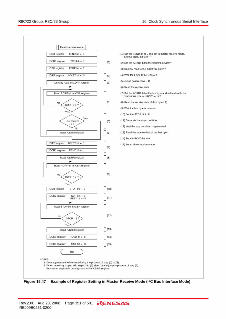
R8C/22 Group, R8C/23 Group 16. Clock Synchronous Serial Interface
Rev.2.00 Aug 20, 2008 Page 351 of 501REJ09B0251-0200
Figure 16.47 Example of Register Setting in Master Receive Mode (I2C Bus Interface Mode)
End
RDRF = 1 ?
Master receive mode
No
Yes
(1) Set the TEND bit to 0 and set to master receive mode. Set the TDRE bit to 0(1,2)
(2) Set the ACKBT bit to the transmit device(1)
(3) Dummy-read to the ICDRR register(1)
(4) Wait for 1 byte to be received
(5) Judge (last receive - 1)
(6) Read the receive data
(7) Set the ACKBT bit of the last byte and set to disable thecontinuous receive (RCVD = 1)(2)
(8) Read the receive data of (last byte - 1)
(9) Wait the last byte is received
(10) Set the STOP bit to 0
(11) Generate the stop condition
(12) Wait the stop condition is generated
(13) Read the receive data of the last byte
(14) Set the RCVD bit to 0
(15) Set to slave receive mode
ICCR1 register TRS bit ← 0
Dummy-read in ICDRR register
Read RDRF bit in ICSR register
Last receive - 1 ?
ICSR register TEND bit ← 0
ICSR register STOP bit ← 0
ICCR2 register SCP bit ← 0 BBSY bit ← 0
Read STOP bit in ICSR register
STOP = 1 ?
ICSR register TDRE bit ← 0
No
(1)
(2)
(3)
(4)
(5)
(6)
(7)
(8)
(12)
(10)
(13)
(14)
(11)
(9)
(15)
ICIER register ACKBT bit ← 0
No
Yes
Read ICDRR register
ICIER register ACKBT bit ← 1
ICCR1 register RCVD bit ← 1
Read ICDRR register
Read RDRF bit in ICSR register
RDRF = 1 ?
Read ICDRR register
ICCR1 register RCVD bit ← 0
ICCR1 register MST bit ← 0
No
Yes
Yes
NOTES:1. Do not generate the interrupt during the process of step (1) to (3).2. When receiving 1 byte, skip step (2) to (6) after (1) and jump to process of step (7). Process of step (8) is dummy-read in the ICDRR register.

R8C/22 Group, R8C/23 Group 16. Clock Synchronous Serial Interface
Rev.2.00 Aug 20, 2008 Page 352 of 501REJ09B0251-0200
Figure 16.48 Example of Register Setting in Slave Transmit Mode (I2C Bus Interface Mode)
End
Write transmit data to ICDRT register
Slave transmit mode
No
Yes
(1) Set the AAS bit to 0
(2) Set the transmit data (except the last byte)
(3) Wait the ICDRT register is empty
(4) Set the transmit data of the last byte
(5) Wait the last byte is transmitted
(6) Set the TEND bit to 0
(7) Set to slave receive mode
(8) Dummy-read in the ICDRR register to release theSCL signal
(9) Set the TDRE bit to 0
TDRE = 1 ?
Read TDRE bit in ICSR register
Last byte ?
Write transmit data to ICDRT register
TEND = 1 ?
Read TEND bit in ICSR register
ICSR register TEND bit ← 0
ICSR register AAS bit ← 0
ICCR1 register TRS bit ← 0
ICSR Register TDRE Bit ← 0
No
Yes
No
Yes
(1)
(2)
(3)
(4)
(5)
(6)
(7)
(8)
(9)
Dummy-read in ICDRR register

R8C/22 Group, R8C/23 Group 16. Clock Synchronous Serial Interface
Rev.2.00 Aug 20, 2008 Page 353 of 501REJ09B0251-0200
Figure 16.49 Example of Register Setting in Slave Receive Mode (I2C Bus Interface Mode)
End
RDRF = 1 ?
Slave receive mode
No
Yes
(1) Set the AAS bit to 0(1)
(2) Set the ACKBT bit to the transmit device
(3) Dummy-read to the ICDRR register
(4) Wait 1 byte is received
(5) Judge (last receive - 1)
(6) Read the receive data
(7) Set the ACKBT bit of the last byte(1)
(8) Read the receive data of (last byte - 1)
(9) Wait the last byte is received
(10) Read the receive data of the last byte
Dummy-read in ICDRR register
Read RDRF bit in ICSR register
Last receive - 1 ?
(1)
(2)
(3)
(4)
(5)
(6)
(7)
(8)
(10)
(9)
ICIER register ACKBT bit ← 0
No
Yes
Read ICDRR register
ICIER register ACKBT bit ← 1
Read ICDRR register
Read RDRF bit in ICSR register
RDRF = 1 ?
Read ICDRR register
No
Yes
NOTE: 1. When receiving 1 byte, skip steps (2) to (6) after (1) and jump to process of step (7). Process of step (8) is dummy-read in the ICDRR register.
ICSR register AAS bit ← 0

R8C/22 Group, R8C/23 Group 16. Clock Synchronous Serial Interface
Rev.2.00 Aug 20, 2008 Page 354 of 501REJ09B0251-0200
16.3.8 Notes on I2C Bus InterfaceSet the IICSEL bit in the PMR register to 1 (select I2C bus interface function) to use I2C bus interface.
16.3.8.1 Multimaster OperationThe following actions must be performed to use the I2C bus interface in multimaster operation.
• Transfer rateSet the transfer rate by 1/1.8 or faster than the fastest rate of the other masters. For example, if the fastesttransfer rate of the other masters is set to 400 kbps, the I2C-bus transfer rate in this MCU should be set to223 kbps (= 400/1.18) or more.
• Bits MST and TRS in the ICCR1 register setting(a) Use the MOV instruction to set bits MST and TRS.(b) When arbitration is lost, confirm the contents of bits MST and TRS. If the contents are other than the
MST bit set to 0 and the TRS bit set to 0 (slave receive mode), set the MST bit to 0 and the TRS bit to 0again.
16.3.8.2 Master Receive ModeEither of the following actions must be performed to use the I2C bus interface in master receive mode.
(a) In master receive mode while the RDRF bit in the ICSR register is set to 1, read the ICDRR registerbefore the rising edge of the 8th clock.
(b) In master receive mode, set the RCVD bit in the ICCR1 register to 1 (disables the next receiveoperation) to perform 1-byte communications.

R8C/22 Group, R8C/23 Group 17. Hardware LIN
Rev.2.00 Aug 20, 2008 Page 355 of 501REJ09B0251-0200
17. Hardware LINThe hardware LIN performs LIN communication in cooperation with timer RA and UART0.
17.1 FeaturesThe hardware LIN has the following features.Figure 17.1 shows a Block Diagram of Hardware LIN.
[Master mode]• Generates Synch Break• Detects bus collision
[Slave mode]• Detects Synch Break• Measures Synch Field• Controls Synch Break and Synch Field signal inputs to UART0• Detects bus collision
NOTE: 1. The WakeUp function is detected by INT1.
Figure 17.1 Block Diagram of Hardware LIN
Timer RA
UART0
InterruptcontrolcircuitBus collision
detectioncircuit
Synch Fieldcontrolcircuit
RXD0 pin
TXD0 pin
LSTART bitSBE bitLINE bit Timer RA
interrupt
TIOSEL = 0
Hardware LIN
TIOSEL = 1
RXD data
Timer RAunderflow signal
BCIE, SBIE,and SFIE bits
UART0 transfer clockUART0 TE bit
Timer RA output pulse
UART0 TXD data
MST bit
[Legend]LINE, MST, SBE, LSTART, BCIE, SBIE, SFIE: LINCR register bitsTIOSEL: TRAIOC register bitTE: U0C1 register bit
RXD0 inputcontrolcircuit

R8C/22 Group, R8C/23 Group 17. Hardware LIN
Rev.2.00 Aug 20, 2008 Page 356 of 501REJ09B0251-0200
17.2 Input/Output PinsTable 17.1 lists the Pin Configuration of the hardware LIN.
Table 17.1 Pin Configuration
Name Abbreviation Input/Output Function
Receive Data Input RXD0 Input Receive data input pin of the hardware LIN
Transmit Data Output TXD0 Output Transmit data output pin of the hardware LIN

R8C/22 Group, R8C/23 Group 17. Hardware LIN
Rev.2.00 Aug 20, 2008 Page 357 of 501REJ09B0251-0200
17.3 Register ConfigurationThe hardware LIN contains the following registers.
• LIN Control Register (LINCR)• LIN Status Register (LINST)
Figure 17.2 and Figure 17.3 show the LINCR and LINST Registers.
Figure 17.2 LINCR Register
LIN Control Register
Symbol Address After ResetLINCR 0106h 00h
Bit Symbol Bit Name Function RW
NOTES:1.2.3. Input to timer RA and UART0 are prohibited immediately after the LINE bit is set to 1(Causes LIN to start operating).
Refer to Figure 17.5 Example of Header Field Transmission Flowchart (1) and Figure 17.9 Example ofHeader Field Reception Flowchart (2).
After setting the LSTART bit, confirm that the RXDSF flag is set to 1 before Synch Break input starts.
SBIE
BCIE
RXDSF
LSTART
0 : Unmasked after Synch Break is detected1 : Unmasked after Synch Field measurement is completed
Synch Break detection interruptenable bit
0 : Disables bus collision detection interrupt1 : Enables bus collision detection interrupt0 : RXD0 input enabled1 : RXD0 input disabledWhen this bit is set to 1, Timer RA input isenabled and RXD0 input is disabled.When read, its content is 0.
RxD0 input status f lag
Synch Break detection start bit(1)
SFIE
0 : Disables Synch Break detection interrupt1 : Enables Synch Break detection interrupt
0 : Disables Synch Field measurement- completed interrupt1 : Enables Synch Field measurement- completed interrupt
RW
RW
RW
WO
RO
RW
RxD0 input unmasking timingselect bit(effective in only slave mode)
b3 b2 b1 b0
SBE
Bus collision detection interruptenable bit
b7 b6 b5 b4
Before changing LIN operation modes, temporarily stop the LIN operation (LINE bit = 0).
Synch Field measurement-completed interrupt enable bit
MST RW
LINELIN operation start bit 0 : Causes LIN to stop
1 : Causes LIN to start operating(3) RW
LIN operation mode setting bit(2) 0 : Slave mode (Synch Break detection circuit actuated)1 : Master mode (timer RA output OR’ed w ith TxD0)

R8C/22 Group, R8C/23 Group 17. Hardware LIN
Rev.2.00 Aug 20, 2008 Page 358 of 501REJ09B0251-0200
Figure 17.3 LINST Register
LIN Status Register
Symbol Address After ResetLINST 0107h 00h
Bit Symbol Bit Name Function RW
Nothing is assigned. If necessary, set to 0.When read, the content is 0.
B2CLR
SBDCT
BCDCT
B0CLR
B1CLR
When this bit is set to 1, BCDCT bit is set to0.When read, its content is 0.
Synch Break detection f lag
Bus collision detection f lagSFDCT flag clear bit
RO
SBDCT flag clear bit
BCDCT flag clear bit
1 show s Synch Break detected or SynchBreak generation completed1 show s Bus collision detectedWhen this bit is set to 1, SFDCT bit is set to 0.When read, its content is 0.When this bit is set to 1, SBDCT bit is set to 0.When read, its content is 0.
b7 b6 b5 b4 b3 b2 b1 b0
—(b7-b6) —
1 show s Synch Field measurement completed.SFDCT
Synch Field measurement-completed f lag RO
WO
WO
WO
RO

R8C/22 Group, R8C/23 Group 17. Hardware LIN
Rev.2.00 Aug 20, 2008 Page 359 of 501REJ09B0251-0200
17.4 Functional Description
17.4.1 Master ModeFigure 17.4 shows a Typical Operation when Sending a Header Field. Figure 17.5 and Figure 17.6 show anExample of Header Field Transmission Flowchart.When transmitting a header field, the hardware LIN operates as described below.
(1) When the TSTART bit in the TRACR register for timer RA is set by writing 1 in a program, thehardware LIN outputs a low-level signal from the TXD0 pin for the period that is set in the TRAPREand TRA registers for timer RA.
(2) When timer RA underflows upon reaching the terminal count, the hardware LIN reverses the output ofthe TXD0 pin and sets the SBDCT flag in the LINST register to 1. Furthermore, if the SBIE bit in theLINCR register is set to 1, it generates a timer RA interrupt.
(3) The hardware LIN transmits 55h via UART0.(4) The hardware LIN transmits an ID field via UART0 after it finished sending 55h.(5) The hardware LIN performs communication for a response field after it finished sending the ID field.
Figure 17.4 Typical Operation when Sending a Header Field
TXD0 pin
Synch Break
10
SBDCT flag in theLINST register
10
IR bit in the TRAICregister
10
Synch Field IDENTIFIER
(1) (2) (3) (4) (5)
Set by writing 1 to theB1CLR bit in the LINSTregister
Cleared to 0 uponacceptance of interruptrequest or by a program
• When LINE bit = 1 (Causes LIN to start operating), MST bit = 1 (Master mode), SBIE bit = 1(Enables Synch Break detection interrupt)

R8C/22 Group, R8C/23 Group 17. Hardware LIN
Rev.2.00 Aug 20, 2008 Page 360 of 501REJ09B0251-0200
Figure 17.5 Example of Header Field Transmission Flowchart (1)
Timer RA Set to timer modeTMOD0 to 2 bits in TRAMR register ← 000b
Timer RA Set the pulse output level from low to startTEDGSEL bit in TRAIOC register ← 1
Timer RA Set the INT1/TRAIO pin to P1_5TIOSEL bit in TRAIOC register ← 1
Timer RA Set the count source (f1, f2, f8, fOCO)TCK0 to 2 bits in TRAMR register
Timer RA Set the Synch Break widthTRAPRE registerTRA register
Hardware LIN Set to master modeMST bit in LINCR register ← 1
Hardware LIN Set the LIN operation to startLINE bit in LINCR register ← 1
Hardware LIN Set the register to enable interrupts(Bus collision detection, Synch Break detection,Synch Field measurement)BCIE, SBIE, SFIE bits in LINCR register
Hardware LIN Clear the status flags(Bus collision detection, Synch Break detection,Synch Field measurement)B2CLR, B1CLR, B0CLR bits in LINST register ← 1
Set the count source and theTRA and TRAPRE registersas suitable for the SynchBreak period.
During master mode, theSynch Field measurement-completed interrupt cannot beused.
A
Set the TIOSEL bit in theTRAIOC register to 1 in thehardware LIN function.
UART0 Set to transmit/receive mode(Transfer data length: 8 bits, Internal clock, 1 stop bit,Parity disabled)U0MR register
UART0 UART0 Set the BRG count source (f1, f8, f32)U0C0CLK0 to 1 bit
UART0 UART0 Set the bit rateU0BRG register
Hardware LIN Set the LIN operation to stopLINE bit in LINCR register ← 0
Set the BRG count sourceand U0BRG register asappropriate for the bit rate.

R8C/22 Group, R8C/23 Group 17. Hardware LIN
Rev.2.00 Aug 20, 2008 Page 361 of 501REJ09B0251-0200
Figure 17.6 Example of Header Field Transmission Flowchart (2)
Timer RA Set the timer to start countingTSTART bit in TRACR register ← 1
Timer RA Read the count status flagTCSTF flag in TRACR register
Hardware LIN Read the Synch Break detection flagSBDCT flag in LINST register
Timer RA Set the timer to stop countingSTART bit in TRACR register ← 0
Timer RA Read the count status flagTCSTF flag in TRACR register
UART0 Communication via UART0TE bit in U0C1 register ← 1U0TB register ← 0055h
The timer RA interrupt may be usedto terminate generation of SynchBreak.
Transmit the ID field.
A
TCSTF = 1?
SBDCT = 1?
YES
TCSTF = 0?
YES
UART0 Communication via UART0U0TB register ← ID field
NO
YES
NO
NO
If the TRAPRE and TRA registers fortimer RA do not need to be read orthe register settings do not need tobe changed after writing 0 to theTSTART bit, the procedure forreading TCSTF flag = 0 can beomitted.Zero to one cycle of the timer RAcount source is required after timerRA stops counting before the TCSTFflag is set to 0.
Transmit the Synch Field.
After timer RA Synch Break isgenerated, the timer should be madeto stop counting.
If the TRAPRE and TRA registers fortimer RA do not need to be read orthe register settings do not need tobe changed after writing 1 to theTSTART bit, the procedure forreading TCSTF flag = 1 can beomitted.
Timer RA generates Synch Break.
Zero to one cycle of the timer RAcount source is required after timerRA starts counting before the TCSTFflag is set to 1.
One to two cycles of the CPU clockare required after Synch Breakgeneration completes before theSBDCT flag is set to 1.

R8C/22 Group, R8C/23 Group 17. Hardware LIN
Rev.2.00 Aug 20, 2008 Page 362 of 501REJ09B0251-0200
17.4.2 Slave ModeFigure 17.7 shows a Typical Operation when Receiving a Header Field. Figure 17.8 through Figure 17.10 showan Example of Header Field Reception Flowchart.When receiving a header field, the hardware LIN operates as described below.
(1) Synch Break detection is enabled by writing 1 to the LSTART bit in the LINCR register of the hardwareLIN.
(2) When a low-level signal is input for a duration equal to or greater than the period set in timer RA, thehardware LIN detects it as Synch Break. At this time, the SBDCT flag in the LINST register is set to 1.Furthermore, if the SBIE bit in the LINCR register is set to 1, the hardware LIN generates a timer RAinterrupt. Then it goes to Synch Field measurement.
(3) The hardware LIN receives a Synch Field (55h). At this time, it measures the period of the start bit andbits 0 to 6 by using timer RA. In this case, it is possible to select whether to input the Synch Field signalto RxD0 of UART0 by setting the SBE bit in the LINCR register accordingly.
(4) The hardware LIN sets the SFDCT flag in the LINST register to 1 when it finished measuring the SynchField. Furthermore, if the SFIE bit in the LINCR register is set to 1, it generates a timer RA interrupt.
(5) After it finished measuring the Synch Field, the hardware LIN calculates a transfer rate from the countvalue of timer RA and sets the result in UART0 and sets the TRAPRE and TRA registers of the timerRA back again. Then it receives an ID field via UART0.
(6) The hardware LIN performs communication for a response field after it finished receiving the ID field.
Figure 17.7 Typical Operation when Receiving a Header Field
RXD0 pin
Synch Break
10
RXD0 input forUART0
10
RXDSF flag in theLINCR register
10
Synch Field IDENTIFIER
(2) (3) (5) (6)(4)(1)
SBDCT flag in theLINST register
10
SFDCT flag in theLINST register
10
IR bit in the TRAICregister
10
Set by writing 1 to theB0CLR bit in the LINSTregister
Cleared to 0 when SynchField measurementfinishes
Measure this period
Set by writing 1 tothe B1CLR bit inthe LINST register
Cleared to 0 uponacceptance ofinterrupt request orby a program
Set by writing 1 tothe LSTART bit inthe LINCR register
• When LINE bit = 1 (Causes LIN to start operating), MST bit = 0 (Slave mode), SBIE bit = 1(Enables Synch Break detection interrupt), SFIE bit = 1 (Enables Synch Field measurementcompleted interrupt)

R8C/22 Group, R8C/23 Group 17. Hardware LIN
Rev.2.00 Aug 20, 2008 Page 363 of 501REJ09B0251-0200
Figure 17.8 Example of Header Field Reception Flowchart (1)
Timer RA Set to pulse width measurement modeBits TMOD0 to TMOD2 in the TRAMR register ← 011b
Timer RA Set the pulse width measurement level lowTEDGSEL bit in the TRAIOC register ← 0
Timer RA Set the INT1/TRAIO pin to P1_5TIOSEL bit in the TRAIOC register ← 1
Timer RA Set the count source (f1, f2, f8, fOCO)TCK0 to 2 bits in the TRAMR register
Timer RA Set the Synch Break widthTRAPRE registerTRA register
Hardware LIN Set to slave modeMST bit in the LINCR register ← 0
Hardware LIN Set the LIN operation to startLINE bit in the LINCR register ← 1
Hardware LIN Set the RXD0 input unmasking timing(After Synch Break detection, or after SynchField measurement)SBE bit in the LINCR register
Hardware LIN Set the register to enable interrupts(Bus collision detection, Synch Breakdetection, Synch Field measurement)Bits BCIE, SBIE, SFIE in the LINCR register
Set the count source and the TRAand TRAPRE registers as suitablefor the Synch Break period.
Select the timing at which tounmask the RXD0 input for UART0.If the RXD0 input is chosen to beunmasked after detection of SynchBreak, the Synch Field signal too isinput to UART0.
A
Hardware LIN Set the LIN operation to stopLINE bit in the LINCR register ← 0

R8C/22 Group, R8C/23 Group 17. Hardware LIN
Rev.2.00 Aug 20, 2008 Page 364 of 501REJ09B0251-0200
Figure 17.9 Example of Header Field Reception Flowchart (2)
Timer RA Set to start a pulse width measurementTSTART bit in the TRACR register ← 1
Timer RA Read the count status flagTCSTF flag in the TRACR register
Hardware LIN Set to start Synch Break detectionLSTART bit in the LINCR register ← 1
Hardware LIN Read the RXD0 input status flagRXDSF flag in the LINCR register
A
TCSTF = 1?
YES
RXDSF = 1?
YES
NO
NO
Timer RA waits until the timerstarts counting.
Hardware LIN Clear the status flags(Bus collision detection, Synch Breakdetection, Synch Field measurement)Bits B2CLR, B1CLR, B0CLR in the LINSTregister ← 1
Hardware LIN Read the Synch Break detection flagSBDCT flag in the LINST register
SBDCT = 1?
YES
NO
B
Hard ware LIN detect a SynchBreak.The interrupt of timer RA may beused.When Synch Break is detected,timer RA is reloaded with theinitially set count value.Even if the duration of the input “L”level is shorter than the set period,timer RA is reloaded with theinitially set count value and waitsuntil the next “L” level is input.One to two cycles of the CPU clockare required after Synch Breakdetection before the SBDCT flag isset to 1.When the SBE bit in the LINCRregister is set to 0 (Unmasked afterSynch Break is detected), timer RAmay be used in timer mode afterthe SBDCT flag in the LINSTregister is set to 1 and the RXDSFflag in the LINCR register is set to0.
Hard ware LIN wait until the RXD0input for UART0 is masked.Do not apply “L” level to the RXD pinuntil the RXDSF flag reads 1 afterwriting 1 to the LSTART bit. This isbecause the signal applied duringthis time is input directly to UART0.One to two cycles of the CPU clockand zero to one cycle of the timerRA count source are required afterthe LSTART bit is set to 1 before theRXDSF flag is set to 1.After this, input to timer RA andUART0 is enabled.
Zero to one cycle of the timer RAcount source is required after timerRA starts counting before theTCSTF flag is set to 1.
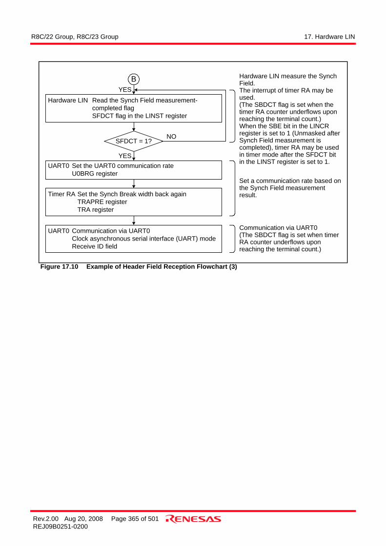
R8C/22 Group, R8C/23 Group 17. Hardware LIN
Rev.2.00 Aug 20, 2008 Page 365 of 501REJ09B0251-0200
Figure 17.10 Example of Header Field Reception Flowchart (3)
Hardware LIN Read the Synch Field measurement-completed flagSFDCT flag in the LINST register
UART0 Set the UART0 communication rateU0BRG register
Communication via UART0(The SBDCT flag is set when timerRA counter underflows uponreaching the terminal count.)
B
SFDCT = 1?
YES
UART0 Communication via UART0Clock asynchronous serial interface (UART) modeReceive ID field
NO
Hardware LIN measure the SynchField.The interrupt of timer RA may beused.(The SBDCT flag is set when thetimer RA counter underflows uponreaching the terminal count.)When the SBE bit in the LINCRregister is set to 1 (Unmasked afterSynch Field measurement iscompleted), timer RA may be usedin timer mode after the SFDCT bitin the LINST register is set to 1.
Set a communication rate based onthe Synch Field measurementresult.
YES
Timer RA Set the Synch Break width back againTRAPRE registerTRA register

R8C/22 Group, R8C/23 Group 17. Hardware LIN
Rev.2.00 Aug 20, 2008 Page 366 of 501REJ09B0251-0200
17.4.3 Bus Collision Detection FunctionThe bus collision detection function can be used when UART0 is enabled for transmission (TE bit in the U0C1register = 1). Figure 17.11 shows a Typical Operation when a Bus Collision is Detected.
Figure 17.11 Typical Operation when a Bus Collision is Detected
TXD0 pin 10
RXD0 pin 10
Transfer clock 10
LINE bit in theLINCR register
10
TE bit in the U0C1register
10
BCDCT flag in theLINST register
10
IR bit in the TRAICregister
10
Cleared to 0 uponacceptance of interruptrequest or by a program
Set by writing 1 tothe B2CLR bit in theLINST register
Set to 1 by a program
Set to 1 by a program

R8C/22 Group, R8C/23 Group 17. Hardware LIN
Rev.2.00 Aug 20, 2008 Page 367 of 501REJ09B0251-0200
17.4.4 Hardware LIN End ProcessingFigure 17.12 shows an Example of Hardware LIN Communication Completion Flowchart.Use the following timing for hardware LIN end processing:
• If the hardware bus collision detection function is usedPerform hardware LIN end processing after checksum transmission completes.
• If the bus collision detection function is not usedPerform hardware LIN end processing after header field transmission and reception complete.
Figure 17.12 Example of Hardware LIN Communication Completion Flowchart
Hardware LIN Clear the status flags(Bus collision detection, Synch Break detection, SynchField measurement)Bits B2CLR, B1CLR, B0CLR in the LINST register ← 1
Timer RA Read the count status flagTCSTF flag in TRACR register
UART0 Complete transmission via UART0When the bus collision detectionfunction is not used, endprocessing for the UART0transmission is not required.
TCSTF = 0 ?
YES
NO
Set the timer to stop counting.
Zero to one cycle of the timer RAcount source is required after timerRA starts counting before theTCSTF flag is set to 1.
After clearing hardware LINstatus flag, stop thehardware LIN operation.
Timer RA Set the timer to stop countingTSTART bit in TRACR register ← 0
Hardware LIN Set the LIN operation to stopLINE bit in the LINCR register ← 0

R8C/22 Group, R8C/23 Group 17. Hardware LIN
Rev.2.00 Aug 20, 2008 Page 368 of 501REJ09B0251-0200
17.5 Interrupt RequestsThere are four interrupt requests that are generated by the hardware LIN: Synch Break detection, Synch Breakgeneration completed, Synch Field measurement, and bus collision detection. These interrupts are shared with thetimer RA interrupt.Table 17.2 lists the Interrupt Requests of Hardware LIN.
Table 17.2 Interrupt Requests of Hardware LIN
Interrupt Request Status Flag Cause of Interrupt
Synch Break Detection SBDCT Generated when timer RA has underflowed after measuring the low level duration of RXD0 input, or when a low-level signal is input for a duration longer than the Synch Break period during communication.
Synch Break Generation Completed
Generated when timer RA has completed outputting a low-level signal to TXD0 for set period.
Synch Field Measurement SFDCT Generated when measurement for 8 bits of the Synch Field by timer RA is completed.
Bus Collision Detection BCDCT Generated when the RXD0 input and TXD0 output values differed at data latch timing while UART0 is enabled for transmission.

R8C/22 Group, R8C/23 Group 17. Hardware LIN
Rev.2.00 Aug 20, 2008 Page 369 of 501REJ09B0251-0200
17.6 Notes on Hardware LINFor the time-out processing of the header and response fields, use another timer to measure the duration of timewith respect to a Synch Break detection interrupt as the starting point.

R8C/22 Group, R8C/23 Group 18. CAN Module
Rev.2.00 Aug 20, 2008 Page 370 of 501REJ09B0251-0200
18. CAN ModuleThe CAN (Controller Area Network) module for the R8C/22 Group, R8C/23 Group of MCUs is a communicationcontroller implementing the CAN 2.0B protocol. The R8C/22 Group, R8C/23 Group contains one Full CAN modulewhich can transmit and receive messages in both standard (11-bit) ID and extended (29-bit) ID formats.Figure 18.1 shows a Block Diagram of CAN Module.External CAN bus driver and receiver are required.
Figure 18.1 Block Diagram of CAN Module
CTx/CRx : CAN I/O pins.Protocol controller : This controller handles the bus arbitration and the CAN protocol services, i.e. bit
timing, stuffing, error status etc.Message box : This memory block consists of 16 slots that can be configured either as transmitter or
receiver. Each slot contains an individual ID, data length code, a data field (8 bytes)and a time stamp.
Acceptance filter : This block performs filtering operation for received messages. For the filteringoperation, the C0GMR register, the C0LMAR register, or the C0LMBR register isused.
16 bit timer : Used for the time stamp function. When the received message is stored in the messagememory, the timer value is stored as a time stamp.
Wake up function : CAN0 wake up interrupt is generated by a message from the CAN bus.Interrupt generation function: The interrupt events are provided by the CAN module. CAN0 successful reception
interrupt, CAN0 successful transmission interrupt, CAN0 error interrupt, and CAN0wake up interrupt.
C0CONR register
C0MCTLj register
C0IDR register
Message boxslot 0 to 15
C0GMR register
C0LMAR register
C0LMBR register
Interruptcontrol logic
C0ICR registerC0STR register
Wakeuplogic
C0RECR register
C0TECR register
CTx
CRx
CAN0 receptionsuccessful interruptCAN0 transmissionsuccessful interruptCAN0 error interruptCAN0 wakeup interrupt
Protocol controller
Data bus
Data Bus
Message IDDLC
Message datatime stamp
Acceptance filterslot 0 to 15
16 bit timer
C0SSTR register
C0CTLR register
j = 0 to 15

R8C/22 Group, R8C/23 Group 18. CAN Module
Rev.2.00 Aug 20, 2008 Page 371 of 501REJ09B0251-0200
18.1 CAN Module-Related RegistersThe CAN0 module has the following registers.
(1) CAN Message BoxA CAN module is equipped with 16 slots (16 bytes or 8 words each). Slots 14 and 15 can be used as BasicCAN.
• Priority of the slots: The smaller the number of the slot, the higher the priority, in both transmission andreception.
• A program can define whether a slot is defined as transmitter or receiver.
(2) Acceptance Mask RegistersA CAN module is equipped with 3 masks for the acceptance filter.
• CAN0 global mask register (C0GMR register: 6 bytes)Configuration of the masking condition for acceptance filtering processing to slots 0 to 13
• CAN0 local mask A register (C0LMAR register: 6 bytes)Configuration of the masking condition for acceptance filtering processing to slot 14
• CAN0 local mask B register (C0LMBR register: 6 bytes)Configuration of the masking condition for acceptance filtering processing to slot 15
(3) CAN SFR Registers
• CAN0 message control register i (C0MCTLi register: 8 bits x 16) (i = 0 to 15)Control of transmission and reception of a corresponding slot
• CAN0 control register (C0CTLR register: 16 bits)Control of the CAN protocol
• CAN0 status register (C0STR register: 16 bits)Indication of the protocol status
• CAN0 slot status register (C0SSTR register: 16 bits)Indication of the status of contents of each slot
• CAN0 interrupt control register (C0ICR register: 16 bits)Selection of interrupt enabled or disabled for each slot
• CAN0 extended ID register (C0IDR register: 16 bits)Selection of ID format (standard or extended) for each slot
• CAN0 configuration register (C0CONR register: 16 bits)Configuration of the bus timing
• CAN0 receive error count register (C0RECR register: 8 bits)Indication of the error status of the CAN module in reception: the counter value is incremented ordecremented according to the error occurrence.
• CAN0 transmit error count register (C0TECR register: 8 bits)Indication of the error status of the CAN module in transmission: the counter value is incremented ordecremented according to the error occurrence.
• CAN0 acceptance filter support register (C0AFS register: 16 bits)Decoding the received ID for use by the acceptance filter support unit
Explanation of each register is given below.

R8C/22 Group, R8C/23 Group 18. CAN Module
Rev.2.00 Aug 20, 2008 Page 372 of 501REJ09B0251-0200
18.2 CAN0 Message BoxTable 18.1 shows the Memory Mapping of CAN0 Message Box.It is possible to access to the message box in byte or word.Mapping of the message contents differs from byte access to word access. Byte access or word access can beselected by the MsgOrder bit of the C0CTLR register.
n: Slot number, n = 0 to 15
Table 18.1 Memory Mapping of CAN0 Message Box
Address Message Content (Memory Mapping)
CAN0 Byte access (8 bits) Word access (16 bits)
1360h + n • 16 + 0 SID10 to SID6 SID5 to SID0
1360h + n • 16 + 1 SID5 to SID0 SID10 to SID6
1360h + n • 16 +2 EID17 to EID14 EID13 to EID6
1360h + n • 16 + 3 EID13 to EID6 EID17 to EID14
1360h + n • 16 + 4 EID5 to EID0 Data Length Code (DLC)
1360h + n • 16 + 5 Data Length Code (DLC) EID5 to EID0
1360h + n • 16 + 6 Data byte 0 Data byte 1
1360h + n • 16 + 7
1360h + n • 16 + 13
Data byte 1
Data byte 7
Data byte 0
Data byte 6
1360h + n • 16 + 14 Time stamp high-order byte Time stamp low-order byte
1360h + n • 16 + 15 Time stamp low-order byte Time stamp high-order byte
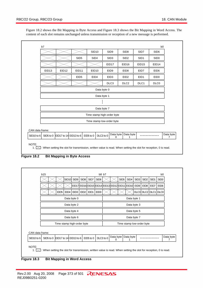
R8C/22 Group, R8C/23 Group 18. CAN Module
Rev.2.00 Aug 20, 2008 Page 373 of 501REJ09B0251-0200
Figure 18.2 shows the Bit Mapping in Byte Access and Figure 18.3 shows the Bit Mapping in Word Access. Thecontent of each slot remains unchanged unless transmission or reception of a new message is performed.
Figure 18.2 Bit Mapping in Byte Access
Figure 18.3 Bit Mapping in Word Access
SID10 to 6 SID5 to 0 EID17 to 14 EID13 to 6 EID5 to 0 DLC3 to 0 Data byte0
Data byte1
Data byte7
SID10 SID9 SID8 SID7 SID6
SID5 SID4 SID3 SID2 SID1 SID0
EID17 EID16 EID15 EID14
EID13 EID12 EID11 EID10 EID9 EID8 EID7 EID6
EID5 EID4 EID3 EID2 EID1 EID0
DLC3 DLC2 DLC1 DLC0
Data byte 0
Data byte 1
Data byte 7
Time stamp high-order byte
Time stamp low-order byte
b7 b0
CAN data frame:
NOTE:1. : When setting the slot for transmission, written value is read. When setting the slot for reception, 0 is read.
EID4 EID2 EID0 DLC2 DLC0
EID17 EID14 EID12 EID10 EID7 EID6
SID10 SID9 SID8 SID7 SID6
b15 b0
SID5 SID4 SID3 SID2 SID1 SID0
EID9 EID8EID11EID13EID15EID16
DLC1DLC3EID1EID3EID5
b8 b7
SID10 to 6 SID5 to 0 EID17 to 14 EID13 to 6 EID5 to 0 DLC3 to 0 Data byte0
Data byte1
Data byte7
Data byte 0
Data byte 2
Data byte 4
Data byte 6
Time stamp high-order byte
CAN data frame:
Data byte 1
Data byte 3
Data byte 5
Data byte 7
Time stamp low-order byte
NOTE:1. : When setting the slot for transmission, written value is read. When setting the slot for reception, 0 is read.

R8C/22 Group, R8C/23 Group 18. CAN Module
Rev.2.00 Aug 20, 2008 Page 374 of 501REJ09B0251-0200
18.3 Acceptance Mask RegistersFigure 18.4 and Figure 18.5 show the C0GMR register, the C0LMAR register, and the C0LMBR register, in whichbit mapping in byte access and word access are shown.
Figure 18.4 Bit Mapping of Mask Registers in Byte Access
Figure 18.5 Bit Mapping of Mask Registers in Word Access
NOTES:1. : Undefined2. Registers C0GMR, C0LMAR, and C0LMBR can be written in CAN reset/initialization mode of the CAN module.
SID10 SID9 SID8 SID7 SID6
SID5 SID4 SID3 SID2 SID1 SID0
EID17 EID16 EID15 EID14
EID13 EID12 EID11 EID10 EID9 EID8 EID7 EID6
EID5 EID4 EID3 EID2 EID1 EID0
146Ch
146Dh
146Eh
146Fh
1470h
C0LMBRregister
SID10 SID9 SID8 SID7 SID6
SID5 SID4 SID3 SID2 SID1 SID0
EID17 EID16 EID15 EID14
EID13 EID12 EID11 EID10 EID9 EID8 EID7 EID6
EID5 EID4 EID3 EID2 EID1 EID0
b7 b0
1460h
1461h
1462h
1463h
1464h
AddressesCAN0
C0GMRregister
SID10 SID9 SID8 SID7 SID6
SID5 SID4 SID3 SID2 SID1 SID0
EID17 EID16 EID15 EID14
EID13 EID12 EID11 EID10 EID9 EID8 EID7 EID6
EID5 EID4 EID3 EID2 EID1 EID0
1466h
1467h
1468h
1469h
146Ah
C0LMARregister
1460h
1462h
1464hEID4 EID2 EID0
EID17 EID14 EID12 EID10 EID7 EID6
SID10 SID9 SID8 SID7 SID6
b15 b0
SID5 SID4 SID3 SID2 SID1 SID0
EID9 EID8EID11EID13EID15EID16
EID1EID3EID5
b8 b7 AddressesCAN0
C0GMRregister
1466h
1468h
146AhEID4 EID2 EID0
EID17 EID14 EID12 EID10 EID7 EID6
SID10 SID9 SID8 SID7 SID6 SID5 SID4 SID3 SID2 SID1 SID0
EID9 EID8EID11EID13EID15EID16
EID1EID3EID5
C0LMARregister
146Ch
146Eh
1470hEID4 EID2 EID0
EID17 EID14 EID12 EID10 EID7 EID6
SID10 SID9 SID8 SID7 SID6 SID5 SID4 SID3 SID2 SID1 SID0
EID9 EID8EID11EID13EID15EID16
EID1EID3EID5
C0LMBRregister
NOTES:1. : Undefined2. Registers C0GMR, C0LMAR, and C0LMBR can be written in CAN reset/initialization mode of the CAN module.

R8C/22 Group, R8C/23 Group 18. CAN Module
Rev.2.00 Aug 20, 2008 Page 375 of 501REJ09B0251-0200
18.4 CAN SFR Registers
18.4.1 C0MCTLi Register (i = 0 to 15)Figure 18.6 shows the C0MCTLi Register.
Figure 18.6 C0MCTLi Register
CAN0 Message Control Register i (i = 0 to 15)(1)
Symbol Address After ResetC0MCTL0 to 1300h to 130Fh 00hC0MCTL15Bit Symbol Bit Name Function RW
New Data
Successful reception f lag When set to reception slot0 : The content of the slot is read or still under processing by the CPU1 : The CAN module has stored new data in the slot
RO(2)
SentData
Successful transmissionflag
When set to transmission slot0 : Transmission is not started or completed yet1 : Transmission is successfully completed RO(2)
InvalData
Under reception f lag When set to reception slot0 : The message is valid1 : The message is invalid (The message is being updated)
RO
TrmActive
Under transmission f lag When set to transmission slot0 : Waiting for bus idle or completion of arbitration1 : Transmitting RO
NOTES:1.2.3.
4.
When w rite, set to 0. Each bit is set w hen the CAN module enters the respective state.In Basic CAN mode, the RemActive bit serves as data format identif ication f lag. When receiving a date frame, theRemActive bit is set to 0 and w hen receiving a remote frame, the RemActive bit is set to 1.
RecReq RW
TrmReqTransmission slot requestbit(4)
0 : Not transmission slot1 : Transmission slot RW
RO
Remote framecorresponding slot select bit
0 : Data frame transmission/reception status1 : Remote frame transmission/reception status
b3 b2 b1 b0
MsgLostOverw rite f lag
RO(2)
0 : Not reception slot1 : Reception slot
When set to reception remote frame slot0 : After a remote frame is received, it w ill be answ ered automatically1 : After a remote frame is received, no transmission w ill be started as long as this bit is set to 1 (Not responding)
RW
RW
When set to reception slot0 : No message is overw ritten1 : New message is overw ritten
Reception slot request bit(4)
Auto response lock modeselect bit
b7 b6 b5 b4
One slot can not be defined as reception slot and transmission slot at the same time.
Remote
Set the C0MCTLi register only w hen the CAN module is in CAN operation mode.
RemActive
RspLock
0 : Slot not corresponding to remote frame1 : Slot corresponding to remote frame
Remote frametransmission/receptionstatus f lag(3)

R8C/22 Group, R8C/23 Group 18. CAN Module
Rev.2.00 Aug 20, 2008 Page 376 of 501REJ09B0251-0200
18.4.2 C0CTLR RegisterFigure 18.7 shows the C0CTLR Register.
Figure 18.7 C0CTLR Register
Symbol Address After ResetC0CTLR 1311h XX0X0000b
Bit Symbol Bit Name Function RW
NOTES:1.2.
3.
4.
Set bits TSPreScale and RXOnly only w hen the CAN module is in CAN operation mode.When set the TSReset bit to 1 (forcible reset of time stamp counter), TSReset bit is automatically set to 0 (normaloperation mode) after the C0TSR register is set to 0000h.When set the RetBusOff bit to 1 (Fforcible return from bus off), the RetBusOff bit is automatically set to 0 (normaloperation mode) after registers C0RECR and C0TECR are set to 0000h.
—(b7-b6) —
Nothing is assigned. If necessary, set to 0.When read, the content is indeterminate.
(b15) (b8)b3 b2 b1 b0b7 b6 b5 b4
Return from bus off commandbit(3)
RW
Listen-only mode select bit(1)
b1 b0
0 0 : 1 Period of 1 bit time0 1 : 1 Period of 1/2 bit time1 0 : 1 Period of 1/4 bit time1 1 : 1 Period of 1/8 bit time
0 : Nothing is occurred1 : Forcible reset of time stamp counter0 : Nothing is occurred1 : Forcible return from bus off
RW
—
RW
RW
When listen-only mode is selected, do not request a transmission.
Nothing is assigned. If necessary, set to 0.When read, the content is indeterminate.
RXOnly
TSPreScale
TSReset
RetBusOff
—(b4)
0 : Listen-only mode disabled1 : Listen-only mode enabled(4)
Time stamp prescaler(1)
Time stamp counter reset bit(2)
CAN0 Control Register
Symbol Address After ResetC0CTLR 1310h X0000001b
Bit Symbol Bit Name Function RW
NOTES:1.
2.
3.4. Irrespective of setting the PD6 register, P6_1 and P6_2 function as CAN I/O pins.
PortEn RW
—(b7)
0 : Operation mode1 : Reset/initialization modeReset
CAN module reset bit(1)
b3 b2 b1 b0b7 b6 b5 b4
RW
RW
RW
RW
RW
RW0 : Loop back mode disabled1 : Loop back mode enabled0 : Word access1 : Byte access0 : Basic CAN mode disabled1 : Basic CAN mode enabled0 : Bus error interrupt disabled1 : Bus error interrupt enabled
Loop back mode select bit(2)
Message order select bit(2)
Basic CAN mode select bit(2)
Bus error interrupt enable bit(2)
LoopBack
MsgOrder
BasicCAN
BusErrEn
Set bits LoopBack, MsgOrder, BasicCAN, BusErrEn, Sleep, and PortEn only w hen the CAN module is in CANreset/initialization mode.To use CAN0 w ake up interrupt, set bits Sleep and PorEn to 1.
Nothing is assigned. If necessary, set to 0.When read, the content is indeterminate.
Sleep
When set the Reset bit to 1 (CAN reset/initialization mode), check that the State_Reset bit in the C0STR register is setto 1 (reset mode).
0 : Sleep mode disabled1 : Sleep mode enabled; clock supply stopped
Sleep mode select bit(2,3)
—
CAN port enable bit(2,3) 0 : I/O port function1 : CTx/CRx function(4)

R8C/22 Group, R8C/23 Group 18. CAN Module
Rev.2.00 Aug 20, 2008 Page 377 of 501REJ09B0251-0200
18.4.3 C0STR RegisterFigure 18.8 shows the C0STR Register.
Figure 18.8 C0STR Register
CAN0 Status Register
Symbol Address After ResetC0STR 1312h 00h
Bit Symbol Bit Name Function RW
NOTE:1.
RecState RO
b3 b2 b1 b0b7 b6 b5 b4
Mbox
TrmSucc
RecSucc
RO
b3 b2 b1 b0
0 0 0 0 : Slot 00 0 0 1 : Slot 10 0 1 0 : Slot 2 • • • •1 1 1 0 : Slot 141 1 1 1 : Slot 15
0 : No [successful] transmission1 : Transmission successful0 : No [successful] reception1 : Reception successful RO
RO
Active slot bits(1)
Successful transmission f lag(1)
Successful reception f lag(1)
TrmStateTransmission f lag (Transmitter)
RO0 : Idle or receiving1 : During transmission
Reception f lag (Receiver) 0 : Idle or transmitting1 : During reception
Bits TrmSucc and RecSucc change w hen the slot enabled the interrupt in the COICR register completed transmittingor receiving.
Symbol Address After ResetC0STR 1313h X0000001b
Bit Symbol Bit Name Function RW
State_BusOff
(b15) (b8)
Nothing is assigned. If necessary, set to 0.When read, the content is indeterminate.
State_ErrPas
0 : No error passive state1 : Error passive state
Error passive state f lag
Bus error state f lag
0 : No loop back mode1 : Loop back mode0 : Word access1 : Byte access
State_LoopBack
State_MsgOrder
State_BasicCAN
State_BusError
RO
—
ROError bus off state f lag 0 : No bus off state
1 : Bus off state
Loop back state f lag
Message order state f lag
Basic CAN mode state f lag 0 : No Basic CAN mode1 : Basic CAN mode
b7 b6 b5 b4 b3 b2 b1 b0
RO
RO
RO
—(b7)
0 : Operation mode1 : Reset mode
State_Reset
Reset state f lag
0 : No error occurred1 : CAN bus error occurred
RO
RO

R8C/22 Group, R8C/23 Group 18. CAN Module
Rev.2.00 Aug 20, 2008 Page 378 of 501REJ09B0251-0200
18.4.4 C0SSTR RegisterFigure 18.9 shows the C0SSTR Register.
Figure 18.9 C0SSTR Register
CAN0 Slot Status Register
Symbol Address After ResetC0SSTR 1315h, 1314h 0000h
Setting values RW
(b8)b0
(b15)b7
0 : Reception slot The message is read Transmission slot Transmission is not completed1 : Reception slot The message is not read Transmission slot Transmission is completed
RO
b7
FunctionSlot status bitsEach bit corresponds to the slot w ith the same number.
b0

R8C/22 Group, R8C/23 Group 18. CAN Module
Rev.2.00 Aug 20, 2008 Page 379 of 501REJ09B0251-0200
18.4.5 C0ICR RegisterFigure 18.10 shows the C0ICR Register.
Figure 18.10 C0ICR Register
18.4.6 C0IDR RegisterFigure 18.11 shows the C0IDR Register.
Figure 18.11 C0IDR Register
CAN0 Interrupt Control Register(1)
Symbol Address After ResetC0ICR 1317h, 1316h 0000h
Setting values RW
NOTE:1.
(b15)b7
0 : Interrupt disabled1 : Interrupt enabled
RW
b7
Function
b0
Set the C0ICR register only w hen the CAN module is in CAN operation mode.
Interrupt enable bits:Each bit corresponds to the slot of the same number asthe bit number.Enabled/disabled successful transmission or receptioninterrupt can be selected.
(b8)b0
CAN0 Extended ID Register(1)
Symbol Address After ResetC0IDR 1319h, 1318h 0000h
Setting values RW
NOTE:1.
(b8)b0
(b15)b7
0 : Standard ID1 : Extended ID
Set the C0IDR register only w hen the CAN module is in CAN operation mode.
b0
RW
Extended ID bits:Each bit corresponds to the slot of the same number asthe bit number.ID format w hich each slot handles can be selected.
b7
Function

R8C/22 Group, R8C/23 Group 18. CAN Module
Rev.2.00 Aug 20, 2008 Page 380 of 501REJ09B0251-0200
18.4.7 C0CONR RegisterFigure 18.12 shows the C0CONR Register.
Figure 18.12 C0CONR Register
CAN0 Configuration Register(2)
Symbol Address After ResetC0CONR 131Ah Indeterminate
Bit Symbol Bit Name Function RW
NOTES:1.
2.
The clock fCAN is used for CAN module. The period is decided by setting the CCLKi bits (i = 0 to 2) in the CCLKRregister.
RW
RW
RW
b7 b6 b5 b4 b3 b2 b1 b0
Set the C0CONR register only w hen the CAN module is in CAN operation mode.
Prescaler division ratio select bits
Sampling control bit
Propagation time segment control bits
BRP
SAM
PTS
b3 b2 b1 b0
0 0 0 0 : fCAN divide-by-1(1)
0 0 0 1 : fCAN divide-by-20 0 1 0 : fCAN divide-by-3 • • • •1 1 1 0 : fCAN divide-by-151 1 1 1 : fCAN divide-by-16
0 : One time sampling1 : Three times sampling
b7 b6 b5
0 0 0 : 1Tq0 0 1 : 2Tq0 1 0 : 3Tq • • •1 1 0 : 7Tq1 1 1 : 8Tq
Symbol Address After ResetC0CONR 131Bh Indeterminate
Bit Symbol Bit Name Function RW
(b15) (b8)
b5 b4 b3
0 0 0 : Do not set0 0 1 : 2Tq0 1 0 : 3Tq • • •1 1 0 : 7Tq1 1 1 : 8Tq
b7 b6
0 0 : 1Tq0 1 : 2Tq1 0 : 3Tq1 1 : 4Tq
PBS2
SJW
Phase buffer segment 2control bits
Re synchronization jump w idthcontrol bits
RW
RW
b7 b6 b5 b4 b3 b2 b1 b0
b2 b1 b0
0 0 0 : Do not set0 0 1 : 2Tq0 1 0 : 3Tq • • •1 1 0 : 7Tq1 1 1 : 8Tq
PBS1
Phase buffer segment 1control bits
RW

R8C/22 Group, R8C/23 Group 18. CAN Module
Rev.2.00 Aug 20, 2008 Page 381 of 501REJ09B0251-0200
18.4.8 C0RECR RegisterFigure 18.13 shows the C0RECR Register.
Figure 18.13 C0RECR Register
18.4.9 C0TECR RegisterFigure 18.14 shows the C0TECR Register.
Figure 18.14 C0TECR Register
CAN0 Receive Error Count Register
Symbol Address After ResetC0RECR 131Ch 00h
Setting Range RW
NOTE:1.
b0
00h to FFh(1) RO
FunctionReception error counting functionThe value is incremented or decremented according tothe CAN module's error status.
The value is indeterminate in bus off state.
b7
CAN0 Transmit Error Count Register
Symbol Address After ResetC0TECR 131Dh 00h
Setting Range RW
NOTE:1.
00h to FFh(1) RO
FunctionTransmission error counting functionThe value is incremented or decremented according tothe CAN module's error status.
The value is indeterminate in bus off state.
b7 b0

R8C/22 Group, R8C/23 Group 18. CAN Module
Rev.2.00 Aug 20, 2008 Page 382 of 501REJ09B0251-0200
18.4.10 C0AFS RegisterFigure 18.15 shows the C0AFS Register.
Figure 18.15 C0AFS Register
CAN0 Acceptance Filter Support Register
Symbol Address After resetC0AFS 1343h, 1342h Indeterminate
Setting values RW
(b8)b0
(b15)b7
Standard ID
b0
RW
b7
FunctionWhen w rite, set the standard ID of received message.When read, its content is the converted value of thestandard ID.

R8C/22 Group, R8C/23 Group 18. CAN Module
Rev.2.00 Aug 20, 2008 Page 383 of 501REJ09B0251-0200
18.5 Operational ModesThe CAN module contains the following four operational modes.
• CAN Reset/Initialization Mode• CAN Sleep Mode• CAN Operation Mode• CAN Interface Sleep Mode
Figure 18.16 shows Transition between Operational Modes.
Figure 18.16 Transition between Operational Modes
18.5.1 CAN Reset/Initialization ModeThe CAN module can enter CAN reset/initialization mode by CPU reset or setting the Reset bit in the C0CTLRregister. When setting the Reset bit to 1, check that the State_Reset bit in the C0STR register is set to 1 duringCAN reset/initialization mode. The CAN module performs the following functions:
• CAN communication is impossible.• If the CAN module is set to CAN reset/initialization mode during transmitting a message, it is held CAN
operation mode until the transmission is completed, it loses in arbitration or an error in it is detected and itenters CAN reset/initialization mode after the State_Reset bit in the C0STR register is set to 0.
• The C0IDR, C0MCTLi (i = 0 to 15), C0ICR, C0STR, C0RECR and C0TECR registers are initialized. Allthese registers are locked to prevent CPU modification.
• The C0CTLR, C0CONR, C0GMR, C0LMAR and C0LMBR registers and the CAN0 message box retaintheir contents and are available for CPU access.
CAN Reset/initialization mode(State_Reset = 1)
CAN Sleep mode
CAN Operationmode
(State_Reset = 0)
Bus off state(State_BusOff = 1)
Sleep = 0 Sleep = 1
CPU Reset
Reset = 0
Reset = 1
TEC > 255
When 11 consecutiverecessive bits are
monitored128 times on the bus or
RetBusOff = 1
CCLK3: Bit in CCLKR registerReset, Sleep, RetBusOff: Bits in C0CTLR registerState_Reset, State_BusOff: Bits in C0STR register
Reset = 1CANInterface Sleep
mode
CCLK3 = 1
CCLK3 = 0

R8C/22 Group, R8C/23 Group 18. CAN Module
Rev.2.00 Aug 20, 2008 Page 384 of 501REJ09B0251-0200
18.5.2 CAN Operation ModeThe CAN module can enter CAN operation mode when the Reset bit in the C0CTLR register is set to 0. Whenset the Reset bit to 0, check that the State_Reset bit in the C0STR register is set to 0. The CAN moduleperforms the following functions after 11 consecutive bits are detected in CAN operation mode.
• The module can transmit and receive a message.• The module controls the error status by counting transmission and reception errors. CAN communication
depends on the error status.The module is placed in one of three sub modes in CAN operation mode.
• Idle mode: Every nodes do nothing. • Receive mode: The node can receive a message transmitted by another node. • Transmit mode: The node can transmit a message. The node can receive own transmitting message
simultaneously when the LoopBack bit in the C0CTLR register is set to 1 (Loop back mode).Figure 18.17 shows Sub Modes in CAN Operation Mode.
Figure 18.17 Sub Modes in CAN Operation Mode
18.5.3 CAN Sleep ModeThe CAN module can enter CAN sleep mode when the Sleep bit in the C0CTLR register is set to 1. Enter CANsleep mode via CAN reset/initialization mode.The power consumption can be reduced because the clock is not provided to the CAN module in CAN sleepmode.
18.5.4 CAN Interface Sleep ModeThe CAN module can enter CAN interface sleep mode when the CCLKR3 bit in the CCLKR register is set to1. Enter CAN interface sleep mode via CAN sleep mode.The power consumption can be reduced because the clock is not provided to CPU interface in the CAN modulewhen entering CAN interface sleep mode.
Lost in arbitration
Idle modeTrmState = 0RecState = 0
Transmit modeTrmState = 1RecState = 0
Receive modeTrmState = 0RecState = 1
TrmState, RecState: Bits in C0STR register
Transmissioncompleted
Transmissionstarts
Receptioncompleted
A SOFdetected

R8C/22 Group, R8C/23 Group 18. CAN Module
Rev.2.00 Aug 20, 2008 Page 385 of 501REJ09B0251-0200
18.5.5 Bus-Off StateWhen repeating communication error, the CAN module enters a bus-off state according to the faultconfinement rule of CAN specification and cannot perform CAN communication. The CAN module can returnto CAN operation mode from a bus-off state in the following conditions. At this time, the value of all CAN-associated registers except the C0STR, C0RECR and C0TECR registers are not changed.
(1) When 11 consecutive recessive bits are monitored 128 timesThe module enters instantly in an error-active state and performs CAN communication.
(2) When the RetBus Off bit in the C0CTLR register = 1 (forcible return form bus off)The module enters instantly in an error-active state and performs CAN communication again after 11consecutive recessive bits are detected.
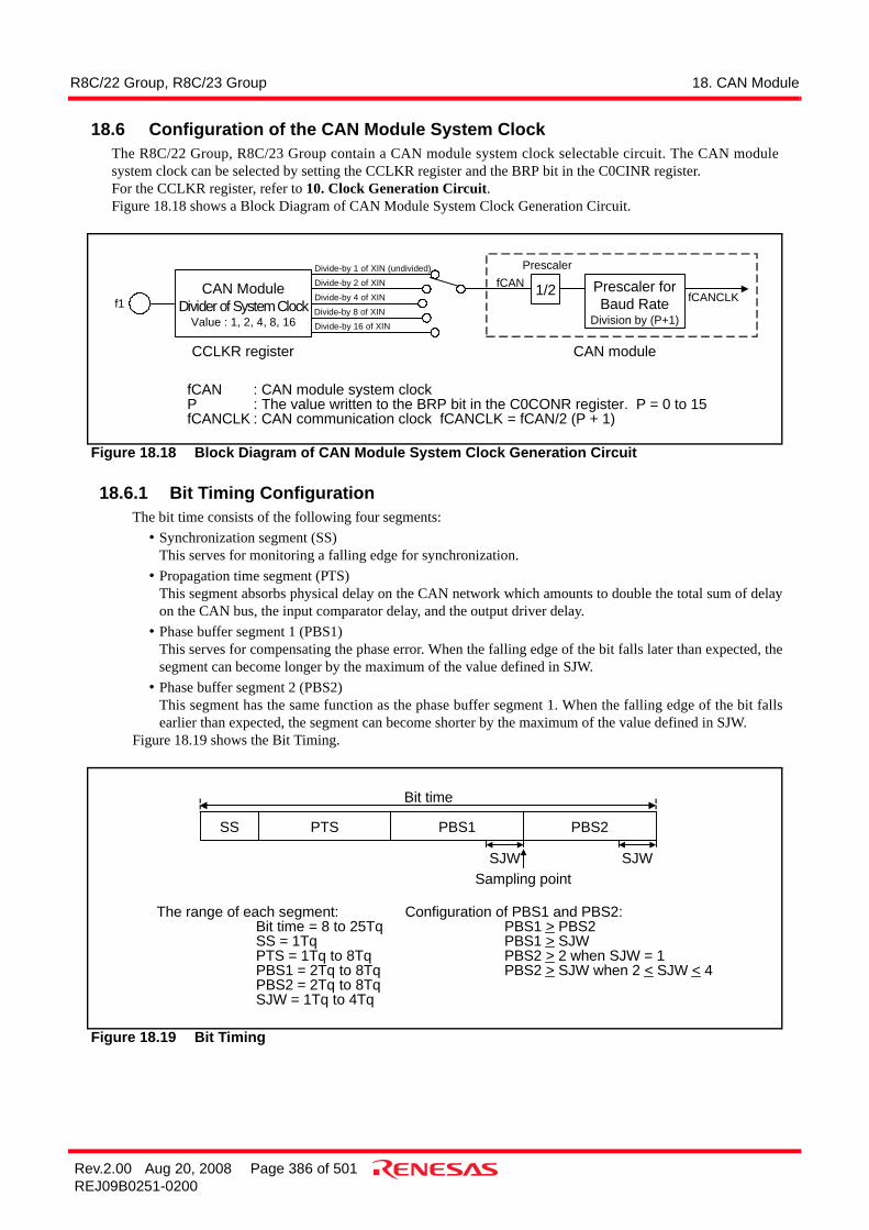
R8C/22 Group, R8C/23 Group 18. CAN Module
Rev.2.00 Aug 20, 2008 Page 386 of 501REJ09B0251-0200
18.6 Configuration of the CAN Module System ClockThe R8C/22 Group, R8C/23 Group contain a CAN module system clock selectable circuit. The CAN modulesystem clock can be selected by setting the CCLKR register and the BRP bit in the C0CINR register.For the CCLKR register, refer to 10. Clock Generation Circuit.Figure 18.18 shows a Block Diagram of CAN Module System Clock Generation Circuit.
Figure 18.18 Block Diagram of CAN Module System Clock Generation Circuit
18.6.1 Bit Timing ConfigurationThe bit time consists of the following four segments:
• Synchronization segment (SS)This serves for monitoring a falling edge for synchronization.
• Propagation time segment (PTS)This segment absorbs physical delay on the CAN network which amounts to double the total sum of delayon the CAN bus, the input comparator delay, and the output driver delay.
• Phase buffer segment 1 (PBS1)This serves for compensating the phase error. When the falling edge of the bit falls later than expected, thesegment can become longer by the maximum of the value defined in SJW.
• Phase buffer segment 2 (PBS2)This segment has the same function as the phase buffer segment 1. When the falling edge of the bit fallsearlier than expected, the segment can become shorter by the maximum of the value defined in SJW.
Figure 18.19 shows the Bit Timing.
Figure 18.19 Bit Timing
Divide-by 1 of XIN (undivided)
Divide-by 4 of XIN
Divide-by 2 of XIN
Divide-by 8 of XINDivide-by 16 of XIN
fCAN : CAN module system clockP : The value written to the BRP bit in the C0CONR register. P = 0 to 15fCANCLK : CAN communication clock fCANCLK = fCAN/2 (P + 1)
f1CAN Module
Divider of System ClockValue : 1, 2, 4, 8, 16
CCLKR register CAN module
fCAN Prescaler forBaud Rate
Division by (P+1)
fCANCLK1/2
Prescaler
The range of each segment:Bit time = 8 to 25TqSS = 1TqPTS = 1Tq to 8TqPBS1 = 2Tq to 8TqPBS2 = 2Tq to 8TqSJW = 1Tq to 4Tq
SS PTS PBS1 PBS2
Bit time
SJWSampling point
SJW
Configuration of PBS1 and PBS2:PBS1 > PBS2PBS1 > SJWPBS2 > 2 when SJW = 1PBS2 > SJW when 2 < SJW < 4

R8C/22 Group, R8C/23 Group 18. CAN Module
Rev.2.00 Aug 20, 2008 Page 387 of 501REJ09B0251-0200
18.6.2 Baud RateBaud rate depends on system clock, the division value of the CAN module system clock, the division value ofthe baud rate prescaler, and the number of Tq’s in one bit.Table 18.2 shows the Examples of Baud Rate.
NOTE:1. The number in ( ) indicates a value of fCAN division value multiplied by division value of the baud
rate prescaler.
Calculation of Baud Rate
XIN2 x fCAN division value(1) x division value of baud rate prescaler(2) x number of Tq’s in one bit
NOTES:1. fCAN division value = 1, 2, 4, 8, 16
fCAN division value: a value selected in the CCLKR register2. Division value of prescaler for baud rate = P + 1 (P: 0 to 15)
P: a value selected by the BRP bit in the C0CONR register
Table 18.2 Examples of Baud Rate
Baud Rate 20 MHz 16 MHz 10 MHz 8 MHz
1 Mbps 10Tq (1) 8Tq (1) --- ---
500 kbps 10Tq (2)20Tq (1)
8Tq (2)16Tq (1)
10Tq (1)---
8Tq (1)---
125 kbps
8Tq (10)10Tq (8)16Tq (5)20Tq (4)
8Tq (8)16Tq (4)
---
8Tq (5)10Tq (4)20Tq (2)
---
8Tq (4)16Tq (2)
---
83.3 kbps8Tq (15)
10Tq (12)20Tq (6)
8Tq (12)16Tq (6)
---
10Tq (6)20Tq (3)
---
8Tq (6)16Tq (3)
---
33.3 kbps
10Tq (30)20Tq (15)
---
8Tq (30)10Tq (24)16Tq (15)20Tq (12)
10Tq (15)---
8Tq (15)10Tq (12)20Tq (6)
---

R8C/22 Group, R8C/23 Group 18. CAN Module
Rev.2.00 Aug 20, 2008 Page 388 of 501REJ09B0251-0200
18.7 Acceptance Filtering Function and Masking FunctionThese functions serve the users to select and receive a facultative message. The C0GMR, C0LMAR, andC0LMBR registers can perform masking to the standard or extended ID. The C0GMR register corresponds to slots0 to 13, the C0LMAR register corresponds to slot 14, and the C0LMBR register corresponds to slot 15. Whenacceptance filtering, the masking function is valid to a received 11 or 29 bit ID by the value set to the slot in theC0IDR register. This function is used for receiving a certain range of IDs.Figure 18.20 shows Correspondence of Mask Registers to Slots and Figure 18.21 shows the Acceptance Function.
Figure 18.20 Correspondence of Mask Registers to Slots
Figure 18.21 Acceptance Function
When using the acceptance function, note the following points.(1) If two or more slots are set the same ID and received a same message, the smallest slot number is valid.(2) If slots 14 and 15 are set to receive all IDs in Basic mode, slots 14 and 15 can receive IDs which are not
received by slots 0 to 13.
Slot #0
Slot #2Slot #3Slot #4Slot #5Slot #6Slot #7Slot #8Slot #9
Slot #10Slot #11Slot #12Slot #13Slot #14Slot #15
Slot #1
C0GMR register
C0LMAR registerC0LMBR register
ID of the receivedmessage
ID stored inthe slot
The value of themask register
Mask Bit Values0 : ID (to which the received message
corresponds) match is handled as“Do not care”.
1 : ID (to which the received messagecorresponds) match is checked.
Acceptance judge signal0 : The CAN module ignores the current
incoming message.(Not stored in any slot)
1 : The CAN module stores the currentincoming message in a slot of which IDmatches.
AcceptanceSignal

R8C/22 Group, R8C/23 Group 18. CAN Module
Rev.2.00 Aug 20, 2008 Page 389 of 501REJ09B0251-0200
18.8 Acceptance Filter Support Unit (ASU)The ASU is a function to determine whether the receive ID is valid or not by means of a table search. To use thisfunction, first register the ID to receive in the data table. Next, store the received ID in the C0AFS register, readout the decoded received ID from the C0AFS register and check it by searching the table. The ASU can only beused for the IDs of standard frames.
The ASU will prove effective in the following cases.• When the IDs to receive cannot be masked by the acceptance filter.
(Example) IDs to receive: 078h, 087h, 111h• When there are too many IDs to receive and filtering in software requires an excessive amount of time.
Figure 18.22 shows the Content of C0AFS Register When Written to and Read out (For Word Access).
Figure 18.22 Content of C0AFS Register When Written to and Read out (For Word Access)
1343h,1342h
SID10 SID9 SID8 SID7 SID6
b15 b0
SID5 SID4 SID3 SID2 SID1 SID0
b8 b7AddressCAN0
When write
1343h,1342h
b15 b0
SID10 SID8 SID7 SID6 SID5 SID4 SID3SID9
b8 b7
When read
3/8 Decoder
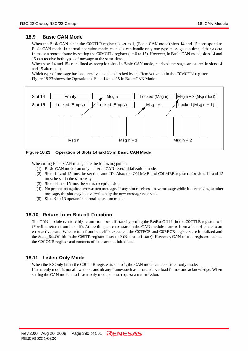
R8C/22 Group, R8C/23 Group 18. CAN Module
Rev.2.00 Aug 20, 2008 Page 390 of 501REJ09B0251-0200
18.9 Basic CAN ModeWhen the BasicCAN bit in the C0CTLR register is set to 1, (Basic CAN mode) slots 14 and 15 correspond toBasic CAN mode. In normal operation mode, each slot can handle only one type message at a time, either a dataframe or a remote frame by setting the C0MCTLi register (i = 0 to 15). However, in Basic CAN mode, slots 14 and15 can receive both types of message at the same time.When slots 14 and 15 are defined as reception slots in Basic CAN mode, received messages are stored in slots 14and 15 alternately.Which type of message has been received can be checked by the RemActive bit in the C0MCTLi register.Figure 18.23 shows the Operation of Slots 14 and 15 in Basic CAN Mode.
Figure 18.23 Operation of Slots 14 and 15 in Basic CAN Mode
When using Basic CAN mode, note the following points.(1) Basic CAN mode can only be set in CAN reset/initialization mode.(2) Slots 14 and 15 must be set the same ID. Also, the C0LMAR and C0LMBR registers for slots 14 and 15
must be set in the same way.(3) Slots 14 and 15 must be set as reception slot.(4) No protection against overwritten message. If any slot receives a new message while it is receiving another
message, the slot may be overwritten by the new message received.(5) Slots 0 to 13 operate in normal operation mode.
18.10 Return from Bus off FunctionThe CAN module can forcibly return from bus off state by setting the RetBusOff bit in the C0CTLR register to 1(Forcible return from bus off). At the time, an error state in the CAN module transits from a bus-off state to anerror-active state. When return from bus-off is executed, the C0TECR and C0RECR registers are initialized andthe State_BusOff bit in the C0STR register is set to 0 (No bus off state). However, CAN related registers such asthe C0CONR register and contents of slots are not initialized.
18.11 Listen-Only ModeWhen the RXOnly bit in the C0CTLR register is set to 1, the CAN module enters listen-only mode.Listen-only mode is not allowed to transmit any frames such as error and overload frames and acknowledge. Whensetting the CAN module to Listen-only mode, do not request a transmission.
EmptySlot 14 Msg n Locked (Msg n) Msg n + 2 (Msg n lost)
Locked (Empty)Slot 15 Locked (Empty) Msg n+1 Locked (Msg n + 1)
Msg n Msg n + 1 Msg n + 2

R8C/22 Group, R8C/23 Group 18. CAN Module
Rev.2.00 Aug 20, 2008 Page 391 of 501REJ09B0251-0200
18.12 Reception and TransmissionConfiguration of CAN Reception and Transmission ModeTable 18.3 shows Configuration of CAN Reception and Transmission Mode.
TrmReq, RecReq, Remote, RspLock, RemActive, RspLock: C0MCTLi register’s (i = 0 to 15) bit
When configuring a slot as a reception slot, note the following points.(1) Before configuring a slot as a reception slot, be sure to set the C0MCTLi registers (i = 0 to 15) to 00h.(2) A received message is stored in a slot that matches the condition first according to the result of reception
mode configuration and acceptance filtering operation. Upon deciding in which slot to store, the smaller thenumber of the slot is, the higher priority it has.
(3) In normal CAN operation mode, when a CAN module transmits a message of which ID matches, the CANmodule never receives the transmitted data. In loop back mode, however, the CAN module receives backthe transmitted data. In this case, the module does not return an ACK.
When configuring a slot as a transmission slot, note the following points.(1) Before configuring a slot as a transmission slot, be sure to set the C0MCTLi registers to 00h.(2) Set the TrmReq bit to 0 (not transmission slot) before rewriting a transmission slot.(3) A transmission slot should not be rewritten when the TrmActive bit is 1 (transmitting). If it is rewritten, an
indeterminate data will be transmitted.
Table 18.3 Configuration of CAN Reception and Transmission Mode
TrmReq RecReq Remote RspLock Communication Mode of the Slot
0 0 ----- ----- Communication environment configuration mode: configure the communication mode of the slot.
0 1 0 0 Configured as a reception slot for a data frame.
1 0 1 0 Configured as a transmission slot for a remote frame. (At this time the RemActive bit is 1.)After completion of transmission, this functions as a reception slot for a data frame. (At this time the RemActive bit is 0.)However, when an ID that matches on the CAN bus is detected before remote frame transmission, this immediately functions as a reception slot for a data frame.
1 0 0 0 Configured as a transmission slot for a data frame.
0 1 1 1/0 Configured as a reception slot for a remote frame. (At this time the RemActive bit is 1.)After completion of reception, this functions as a transmission slot for a data frame. (At this time the RemActive bit is 0.)However, transmission does not start as long as RspLock bit remains 1; thus no automatic remote frame response.Response (transmission) starts when RspLock bit is set to 0.

R8C/22 Group, R8C/23 Group 18. CAN Module
Rev.2.00 Aug 20, 2008 Page 392 of 501REJ09B0251-0200
18.12.1 ReceptionFigure 18.24 shows the Timing of Receive Data Frame Sequence. This is an operation example whenconsecutive messages are received.
Figure 18.24 Timing of Receive Data Frame Sequence
(1) If a SOF is detected on the CAN bus, the RecState bit in the C0STR register is set to 1 (During reception)immediately and the slot starts receiving a message.
(2) The message successfully is received and the NewData bit in the C0MCTLi register of the reception slot isset to 1 (stored new data in slot). The InvalData bit in the C0MCTLi register is set to 1 (the message isbeing updated) at the same time and set to 0 (the message is valid) after the message completely is stored tothe slot.
(3) If the interrupt enable bit in the C0ICR register of the slot is set to 1 (interrupt enabled), the CAN0successful reception interrupt request is generated and the MBOX and RecSucc bits in the C0STR registerchange.
(4) Set the NewData bit to 0 (the content of the slot is read out or still under processing by the CPU) by aprogram and read the message from the slot.
(5) When next CAN message is received before the NewData bit is set to 0 by a program or a receive request toa slot is canceled, the MsgLost bit in the C0MCTLj register is set to 1 (this slot already contained amessage) and new message is stored in a slot. CAN0 successful reception interrupt and the C0STR registerchange the same as (3).
CANbus
RecReq bit
InvalData bit
NewData bit
MsgLost bit
CAN0 successfulreceptioninterrupt
RecState bit
RecSucc bit
MBOX bit C0S
TR re
gist
erC
0MC
TLi r
egis
ter
Receive slot No.
(1)
(3) (5)
(5)
(5)
(4)(2)
(2)
EOF IFSACK SOF EOF IFSACKSOF
i = 0 to 15

R8C/22 Group, R8C/23 Group 18. CAN Module
Rev.2.00 Aug 20, 2008 Page 393 of 501REJ09B0251-0200
18.12.2 TransmissionFigure 18.25 shows the Timing of Transmit Sequence.
Figure 18.25 Timing of Transmit Sequence
(1) If the TrmReq bit in the C0MCTLi register (i = 0 to 15) is set to 1 (Transmission slot) in bus idle state,the TrmActive bit in the C0MCTLi register and the TrmState bit in the C0STR register are set to 1(During transmission), and the CAN module starts transmitting a message.
(2) If the arbitration is lost after starting transmitting, the TrmActive and TrmState bits are set to 0.(3) If the transmission is successful without lost arbitration, the SentData bit in the C0MCTLi register is set
to 1 (Transmission is successfully completed) and TrmActive bit in the C0MCTLi register is set to 0(Waiting for bus idle or completion of arbitration). When the interrupt enable bits in the C0ICR registerare set to 1 (Interrupt enabled), CAN0 successful transmission interrupt request is generated and theMBOX and TrmSucc bits in the C0STR register change.
(4) When next transmission is performed, set the SentData and TrmReq bits to 0 and check that they are setto 0. Then, set the TrmReq bit to 1 by a program.
(4)
CANbus
TrmReq bit
TrmActive bit
SentData bit
CAN0 successfultransmissioninterrupt
TrmState bit
TrmSucc bit
MBOX bit
C0S
TR re
gist
erC
0MC
TLi r
egis
ter
Transmission slotNo.
(3)(2)
EOF IFSACK SOFSOF
(1)
(2)(1)
(1)
(3)
(3)
i = 0 to 15

R8C/22 Group, R8C/23 Group 18. CAN Module
Rev.2.00 Aug 20, 2008 Page 394 of 501REJ09B0251-0200
18.13 CAN InterruptsThe CAN module provides the following CAN interrupts.
• CAN0 Successful Reception Interrupt• CAN0 Successful Transmission Interrupt• CAN0 Error Interrupt
Error Passive StateError BusOff StateBus Error (this feature can be disabled separately)
• CAN0 Wake Up InterruptWhen the CPU detects a successful reception/transmission interrupt, the C0STR register must be read to determinewhich slot has issued the interrupt.

R8C/22 Group, R8C/23 Group 18. CAN Module
Rev.2.00 Aug 20, 2008 Page 395 of 501REJ09B0251-0200
18.14 Notes on CAN Module
18.14.1 Reading C0STR RegisterThe CAN module updates the status of the C0STR register in a certain period. When the CPU and the CANmodule access to the C0STR register at the same time, the CPU has the access priority; the access from theCAN module is disabled. Consequently, when the updating period of the CAN module matches the accessperiod from the CPU, the status of the CAN module cannot be updated. (See Figure 18.26)Accordingly, be careful about the following points so that the access period from the CPU should not match theupdating period of the CAN module:
• There should be a wait time of 3fCAN or longer (see Table 18.4) before the CPU reads the C0STR register.(See Figure 18.27)
• When the CPU polls the C0STR register, the polling period must be 3fCAN or longer. (See Figure 18.28)
Table 18.4 CAN Module Status Updating Period3 fCAN Period = 3 x XIN (Original Oscillation Period) x Division Value of CAN Clock (CCLK)(Example 1) Condition XIN 16 MHz CCLK: Divided by 1 3 fCAN period = 3 x 62.5 ns x 1 = 187.5 ns(Example 2) Condition XIN 16 MHz CCLK: Divided by 2 3 fCAN period = 3 x 62.5 ns x 2 = 375 ns(Example 3) Condition XIN 16 MHz CCLK: Divided by 4 3 fCAN period = 3 x 62.5 ns x 4 = 750 ns(Example 4) Condition XIN 16 MHz CCLK: Divided by 8 3 fCAN period = 3 x 62.5 ns x 8 = 1.5 µs(Example 5) Condition XIN 16 MHz CCLK: Divided by 16 3 fCAN period = 3 x 62.5 ns x 16 = 3 µs

R8C/22 Group, R8C/23 Group 18. CAN Module
Rev.2.00 Aug 20, 2008 Page 396 of 501REJ09B0251-0200
Figure 18.26 When Updating Period of CAN Module Matches Access Period from CPU
Figure 18.27 With a Wait Time of 3fCAN Before CPU Read
Figure 18.28 When Polling Period of CPU is 3fCAN or Longer
fCAN
CPU read signal
CPU reset signal
Updating period ofCAN module
C0STR registerb8: State_Reset bit
0: CAN operation mode
1: CAN reset/initial-ization mode
: When the CAN module’s State_Reset bit updating period matches the CPU’s read period, it does not enter reset mode, for the CPU read has the higher priority.
: Updated without fail in period of 3fCAN
Wait time
CPU read signal
CPU reset signal
Updating period ofCAN module
C0STR registerb8: State_Reset bit
0: CAN operation mode
1: CAN reset/initiall-ization mode
4fCAN
CPU read signal
CPU reset signal
Updating period ofthe CAN module
C0STR registerb8: State_Reset bit
0: CAN operation mode
1: CAN reset/initiall-ization mode
: When the CAN module’s State_Reset bit updating period matches the CPU’s read period, it does not enter reset mode, for the CPU read has the higher priority.
: Updated without fail in period of 4fCAN

R8C/22 Group, R8C/23 Group 18. CAN Module
Rev.2.00 Aug 20, 2008 Page 397 of 501REJ09B0251-0200
18.14.2 Performing CAN ConfigurationIf the Reset bit in the C0CTLR register is changed from 0 (operation mode) to 1 (reset/initialization mode) inorder to place the CAN module from CAN operation mode into CAN reset/initialization mode, always be sureto check that the State_Reset bit in the C0STR register is set to 1 (reset mode).Similarly, if the Reset bit is changed from 1 to 0 in order to place the CAN module from CAN reset/initialization mode into CAN operation mode, always be sure to check that the State_Reset bit is set to 0(operation mode).The procedure is described below.To place CAN Module from CAN Operation Mode into CAN Reset/Initialization Mode
• Change the Reset bit from 0 to 1.• Check that the State_Reset bit is set to 1.
To place CAN Module from CAN Reset/Initialization Mode into CAN Operation Mode• Change the Reset bit from 1 to 0.• Check that the State_Reset bit is set to 0.

R8C/22 Group, R8C/23 Group 18. CAN Module
Rev.2.00 Aug 20, 2008 Page 398 of 501REJ09B0251-0200
18.14.3 Suggestions to Reduce Power ConsumptionWhen not performing CAN communication, the operation mode of CAN transceiver should be set to “standbymode” or “sleep mode”.When performing CAN communication, the power consumption in CAN transceiver in not performing CANcommunication can be substantially reduced by controlling the operation mode pins of CAN transceiver.Table 18.5 and Table 18.6 show Recommended Pin Connections.
NOTES:1. The pin which controls the operation mode of CAN transceiver.2. In case of Topr = 25°C3. Connect to enabled port to control CAN transceiver.
NOTES:1. The pin which controls the operation mode of CAN transceiver.2. In case of Topr = 25°C3. Connect to enabled port to control CAN transceiver.
Table 18.5 Recommended Pin Connections (In Case of PCA82C250: Philips Product)Standby Mode High-speed Mode
Rs Pin(1) “H” “L”Power Consumption in CAN Transceiver(2)
less than 170 µA less than 70 mA
CAN Communication impossible possibleConnection
Table 18.6 Recommended Pin Connections (In Case of PCA82C252: Philips Product)Sleep Mode Normal Operation Mode
STB Pin(1) “L” “H”
EN Pin(1) “L” “H”Power Consumption in CAN Transceiver(2)
less than 50 µA less than 35 mA
CAN Communication impossible possibleConnection
R8C/22, R8C/23PCA82C250
CTX0CRX0
Port(3)
TXDRXD
Rs
CANHCANL
“H”output
PCA82C250
CTX0CRX0
TXDRXD
Rs
CANHCANL
Port(3)
“L” output
R8C/22, R8C/23
PCA82C252
CTX0CRX0
TXDRXD
STB
CANHCANL
EN
Port(3)
Port(3)
R8C/22, R8C/23
“L” output
PCA82C252
CTX0CRX0
TXDRXD
STB
CANHCANL
EN
Port(3)
Port(3)
R8C/22, R8C/23
“H” output

R8C/22 Group, R8C/23 Group 19. A/D Converter
Rev.2.00 Aug 20, 2008 Page 399 of 501REJ09B0251-0200
19. A/D ConverterThe A/D converter consists of one 10-bit successive approximation A/D converter circuit with a capacitive couplingamplifier. The analog input shares the pins with P0_0 to P0_7, P1_0 to P1_3. Therefore, when using these pins, ensurethe corresponding port direction bits are set to 0 (input mode).When not using the A/D converter, set the VCUT bit in the ADCON1 register to 0 (Vref unconnected), so that nocurrent will flow from the VREF pin into the resistor ladder, helping to reduce the power consumption of the chip.The result of A/D conversion is stored in the AD register.Table 19.1 lists the Performance of A/D Converter. Figure 19.1 shows the Block Diagram of A/D Converter. Figure19.2 and Figure 19.3 show the A/D converter-related registers.
NOTES:1. Analog input voltage does not depend on use of sample and hold function.
When analog input voltage exceeds reference voltage, A/D conversion result is 3FFh in 10-bit mode, FFh in 8-bit mode.
2. The frequency of φAD must be 10 MHz or below.Without sample and hold function, the φAD frequency should be 250 kHz or above.With the sample and hold function, the φAD frequency should be 1 MHz or above.
3. In repeat mode, only 8-bit mode can be used.
Table 19.1 Performance of A/D ConverterItem Performance
A/D Conversion Method Successive approximation (with capacitive coupling amplifier)Analog Input Voltage(1) 0 V to AVCCOperating Clock φAD(2) 4.2 V ≤ AVCC ≤ 5.5 V f1, f2, f4, fOCO-F
2.7 V ≤ AVCC < 4.2 V f2, f4, fOCO-FResolution 8 bit or 10 bit is selectableAbsolute Accuracy AVCC = Vref = 5 V, φAD = 10MHz
• 8-bit resolution ±2 LSB• 10-bit resolution ±3 LSBAVCC = Vref = 3.3 V, φAD = 10MHz• 8-bit resolution ±2 LSB• 10-bit resolution ±5 LSB
Operating Mode One-shot and repeat modes(3)
Analog Input Pin 12 pins (AN0 to AN11)A/D Conversion Start Condition • Software trigger
Set the ADST bit in the ADCON0 register to 1 (A/D conversion starts)• Capture
Timer RD interrupt request is generated while the ADST bit is set to 1Conversion Rate Per Pin • Without sample and hold function
8-bit resolution: 49φAD cycles, 10-bit resolution: 59φAD cycles• With sample and hold function
8-bit resolution: 28φAD cycles, 10-bit resolution: 33φAD cycles

R8C/22 Group, R8C/23 Group 19. A/D Converter
Rev.2.00 Aug 20, 2008 Page 400 of 501REJ09B0251-0200
Figure 19.1 Block Diagram of A/D Converter
Comparator
AVSS
Data bus
øAD
Resistor ladder
VCUT = 0
VCUT = 1VREF
Successive conversion register
AD register
ADCON0
Vcom
VIN
P1_0/AN8 CH2 to CH0 = 100b
P1_1/AN9 CH2 to CH0 = 101b
P1_2/AN10 CH2 to CH0 = 110b
P1_3/AN11 CH2 to CH0 = 111b
ADGSEL0 = 1
CH0 to CH2, ADGSEL, CKS0: Bits in ADCON0 registerCKS1, VCUT: Bits in ADCON1 register
A/D conversion rate selection
ADGSEL0 = 0
ADCAP = 1
Software trigger
Timer RD interrupt request
ADCAP = 0
Trigger
P0_7/AN0 CH2 to CH0 = 000b
P0_6/AN1 CH2 to CH0 = 001b
P0_5/AN2 CH2 to CH0 = 010b
P0_4/AN3 CH2 to CH0 = 011b
P0_3/AN4 CH2 to CH0 = 100b
P0_2/AN5 CH2 to CH0 = 101b
P0_1/AN6 CH2 to CH0 = 110b
P0_0/AN7 CH2 to CH0 = 111b
Decoder
CKS0 = 1
CKS1 = 1
CKS1 = 0CKS0 = 0
f2
f4
CKS0 = 0
fOCO-F
f1
CKS0 = 1

R8C/22 Group, R8C/23 Group 19. A/D Converter
Rev.2.00 Aug 20, 2008 Page 401 of 501REJ09B0251-0200
Figure 19.2 ADCON0 Register
A/D Control Register 0(1)
Symbol Address After ResetADCON0 00D6h 00h
Bit Symbol Bit Name Function RW
NOTES:1.2.3.4.
ADGSEL0 = 0 ADGSEL0 = 1AN0AN1AN2AN3AN4 AN8AN5 AN9AN6 AN10AN7 AN11
100b101b110b111b
CH2 to CH0000b Do not set001b010b011b
Set øAD frequency to 10 MHz or below .The analog input pin can be select according to a combination of the CH0 to CH2 bits and the ADGSEL0 bit.
CKS0
Frequency select bit 0 [When CKS1 in ADCON1 register = 0]0 : Select f41 : Select f2[When CKS1 in ADCON1 register = 1]0 : Select f1(3)
1 : Select fOCO-F
RW
If the ADCON0 register is rew ritten during A/D conversion, the conversion result is indeterminate.When changing A/D operation mode, set the analog input pin again.
ADSTA/D conversion start f lag 0 : Disables A/D conversion
1 : Starts A/D conversion RW
ADCAPA/D conversion automaticstart bit
0 : Starts in softw are trigger (ADST bit)1 : Starts in timer RD (complementary PWM mode)
RW
0 : On-shot mode1 : Repeat mode RW
RW
ADGSEL0 RWA/D input group select bit(4) 0 : Selects port P0 group (AN0 to AN7)
1 : Selects port P1 group (AN8 to AN11)
CH1 RWCH0
CH2 RW
Analog input pin select bit Refer to (4)
MDA/D operation mode selectbit(2)
b7 b6 b5 b4 b3 b2 b1 b0

R8C/22 Group, R8C/23 Group 19. A/D Converter
Rev.2.00 Aug 20, 2008 Page 402 of 501REJ09B0251-0200
Figure 19.3 Registers ADCON1, ADCON2, and AD
A/D Control Register 1(1)
Symbol Address After ResetADCON1 00D7h 00h
Bit Symbol Bit Name Function RW
NOTES:1.2.3. When the VCUT bit is set to 1 (connected) from 0 (not connected), w ait for 1 µs or more before starting A/D
conversion.
b3 b2
VCUT
b1 b0
0 0
Refer to a description of the CKS0 bit in theADCON0 register function
b7 b6 b5 b4
—(b2-b0)
0 0 0
If the ADCON1 register is rew ritten during A/D conversion, the conversion result is indeterminate.
CKS1 RW
RW
RW—
(b7-b6)Reserved Bit
Vref connect bit(3) 0 : Vref not connected1 : Vref connected
Set the BITS bit to 0 (8-bit mode) in repeat mode.
Reserved bit Set to 0
8/10-bit mode select bit(2) 0 : 8-bit mode1 : 10-bit mode
RW
Set to 0
Frequency select bit 1
BITS RW
A/D Control Register 2(1)
Symbol Address After ResetADCON2 00D4h 00h
Bit Symbol Bit Name Function RW
NOTE:1.
b0
0 00b3 b2 b1
Reserved bit Set to 0
b7 b6 b5 b4
0 : Without sample and hold1 : With sample and hold RW
If the ADCON2 register is rew ritten during A/D conversion, the conversion result is indeterminate.
SMPA/D conversion method select bit
Nothing is assigned. If necessary, set to 0.When read, the content is 0.
—(b7-b4) —
—(b3-b1) RW
A/D Register
Symbol Address After ResetAD 00C1h-00C0h Indeterminate
RWFunction
RO
When BITS bit in ADCON1 register is set to 1(10-bit mode)
When BITS bit in ADCON1 register is set to 0(8-bit mode)
8 low -order bits in A/D conversion result A/D conversion result
RW
RONothing is assigned. If necessary, set to 0.When read, the content is 0. —
2 high-order bits in A/D conversion result When read, its content is indeterminate
b0b7(b8)
b0(b15)
b7

R8C/22 Group, R8C/23 Group 19. A/D Converter
Rev.2.00 Aug 20, 2008 Page 403 of 501REJ09B0251-0200
19.1 One-Shot ModeIn one-shot mode, the input voltage on one selected pin is A/D converted once.Table 19.2 lists the One-Shot Mode Specifications. Figure 19.4 shows the ADCON0 Register in One-Shot Modeand Figure 19.5 shows the ADCON1 Register in One-Shot Mode.
Table 19.2 One-Shot Mode SpecificationsItem Specification
Function The input voltage on one selected pin by bits CH2 to CH0 and ADGSEL0 is A/D converted once
Start Condition • When the ADCAP bit is set to 0 (software trigger),Set the ADST bit to 1 (A/D conversion starts)
• When the ADCAP bit is set to 1 (starts in timer RD (complementary PWM mode)),The compare match in the TRD0 and TRDGRA0 registers or the TRD1 underflow is generated while the ADST bit is set to 1
Stop Condition • A/D conversion completes (When the ADCAP bit is set to 0 (software trigger), the ADST bit is set to 0)
• Set the ADST bit to 0Interrupt Request Generation Timing
A/D conversion completes
Input Pin Select one of AN0 to AN11Reading of A/D Conversion Result
Read the AD register

R8C/22 Group, R8C/23 Group 19. A/D Converter
Rev.2.00 Aug 20, 2008 Page 404 of 501REJ09B0251-0200
Figure 19.4 ADCON0 Register in One-Shot Mode
A/D Control Register 0(1)
Symbol Address After ResetADCON0 00D6h 00h
Bit Symbol Bit Name Function RW
NOTES:1.2.3.4.
ADGSEL0 = 0 ADGSEL0 = 1AN0AN1AN2AN3AN4 AN8AN5 AN9AN6 AN10AN7 AN11
100b101b110b111b
CH2 to CH0000b Do not set001b010b011b
b0
0b3 b2 b1
MDA/D operation mode selectbit(2)
b7 b6 b5 b4
CH2 RW
Analog input pin select bit Refer to (4)
0 : One-shot modeRW
RW
ADGSEL0 RWA/D input group select bit(4) 0 : Selects port P0 group (AN0 to AN7)
1 : Selects port P1 group (AN8 to AN11)
CH1 RWCH0
ADCAPA/D conversion automaticstart bit
0 : Starts in softw are trigger (ADST bit)1 : Starts in timer RD (complementary PWM mode)
RW
ADSTA/D conversion start f lag 0 : Disables A/D conversion
1 : Starts A/D conversion RW
Set øAD frequency to 10 MHz or below .The analog input pin can be select according to a combination of the CH0 to CH2 bits and the ADGSEL0 bit.
CKS0
Frequency select bit 0 [When CKS1 in ADCON1 register = 0]0 : Select f41 : Select f2[When CKS1 in ADCON1 register = 1]0 : Select f1(3)
1 : Select fOCO-F
RW
If the ADCON0 register is rew ritten during A/D conversion, the conversion result is indeterminate.When changing A/D operation mode, set the analog input pin again.

R8C/22 Group, R8C/23 Group 19. A/D Converter
Rev.2.00 Aug 20, 2008 Page 405 of 501REJ09B0251-0200
Figure 19.5 ADCON1 Register in One-Shot Mode
A/D Control Register 1(1)
Symbol Address After ResetADCON1 00D7h 00h
Bit Symbol Bit Name Function RW
NOTES:1.2. When the VCUT bit is set to 1 (connected) from 0 (not connected), w ait for 1 µs or more before starting A/D
conversion.
b3 b2
VCUT
b1 b0
0 0
Refer to a description of the CKS0 bit in theADCON0 register function
b7 b6 b5 b4
—(b2-b0)
0 0 1 0
BITS RW
If the ADCON1 register is rew ritten during A/D conversion, the conversion result is indeterminate.
CKS1 RW
RW
RW—
(b7-b6)Reserved bitVref connect bit(2)
RW
Set to 0
Frequency select bit 1
1 : Vref connected
Reserved bit Set to 0
8/10-bit mode select bit 0 : 8-bit mode1 : 10-bit mode

R8C/22 Group, R8C/23 Group 19. A/D Converter
Rev.2.00 Aug 20, 2008 Page 406 of 501REJ09B0251-0200
19.2 Repeat ModeIn repeat mode, the input voltage on one selected pin is A/D converted repeatedly.Table 19.3 lists the Repeat Mode Specifications. Figure 19.6 shows the ADCON0 Register in Repeat Mode andFigure 19.7 shows the ADCON1 Register in Repeat Mode.
Table 19.3 Repeat Mode SpecificationsItem Specification
Function The Input voltage on one pin selected by CH2 to CH0 and ADGSEL0 bits is A/D converted repeatedly
Start Condition • When the ADCAP bit is set to 0 (software trigger)Set the ADST bit to 1 (A/D conversion starts)
• When the ADCAP bit is set to 1 (starts in timer RD (complementary PWM mode)),The compare match in the TRD0 and TRDGRA0 registers or the TRD1 underflow is generated while the ADST bit is set to 1
Stop Condition Set the ADST bit to 0Interrupt Request Generation Timing
Not generated
Input Pin Select one of AN0 to AN11Reading of Result of A/D Converter
Read the AD register

R8C/22 Group, R8C/23 Group 19. A/D Converter
Rev.2.00 Aug 20, 2008 Page 407 of 501REJ09B0251-0200
Figure 19.6 ADCON0 Register in Repeat Mode
A/D Control Register 0(1)
Symbol Address After ResetADCON0 00D6h 00h
Bit Symbol Bit Name Function RW
NOTES:1.2.3.4.
ADGSEL0 = 0 ADGSEL0 = 1AN0AN1AN2AN3AN4 AN8AN5 AN9AN6 AN10AN7 AN11
100b101b110b111b
CH2 to CH0000b Do not set001b010b011b
Set øAD frequency to 10 MHz or below .The analog input pin can be select according to a combination of the CH0 to CH2 bits and the ADGSEL0 bit.
CKS0
Frequency select bit 0 [When CKS1 in ADCON1 register = 0]0 : Select f41 : Select f2[When CKS1 in ADCON1 register = 1]0 : Select f1(3)
1 : Do not set
RW
If the ADCON0 register is rew ritten during A/D conversion, the conversion result is indeterminate.When changing A/D operation mode, set the analog input pin again.
ADSTA/D conversion start f lag 0 : Disables A/D conversion
1 : Starts A/D conversion RW
ADCAPA/D conversion automaticstart bit
0 : Starts in softw are trigger (ADST bit)1 : Starts in timer RD (complementary PWM mode)
RW
1 : Repeat modeRW
RW
ADGSEL0 RWA/D input group select bit(4) 0 : Selects port P0 group (AN0 to AN7)
1 : Selects port P1 group (AN8 to AN11)
CH1 RWCH0
CH2 RW
Analog input pin select bit Refer to (4)
MDA/D operating mode selectbit(2)
b7 b6 b5 b4
1b3 b2 b1 b0

R8C/22 Group, R8C/23 Group 19. A/D Converter
Rev.2.00 Aug 20, 2008 Page 408 of 501REJ09B0251-0200
Figure 19.7 ADCON1 Register in Repeat Mode
A/D Control Register 1(1)
Symbol Address After ResetADCON1 00D7h 00h
Bit Symbol Bit Name Function RW
NOTES:1.2.3. When the VCUT bit is set to 1 (connected) from 0 (not connected), w ait for 1 µs or more before starting A/D
conversion.
b3 b2
VCUT
b1 b0
00 0
Refer to a description of the CKS0 bit in theADCON0 register function
b7 b6 b5 b4
—(b2-b0)
0 0 1 0
BITS RW
If the ADCON1 register is rew ritten during A/D conversion, the conversion result is indeterminate.
CKS1 RW
RW
RW—
(b7-b6)Reserved bit
Set the BITS bit to 0 (8-bit mode) in repeat mode.
Vref connect bit(3) 1 : Vref connected
Reserved bit Set to 0
8/10-bit mode select bit(2) 0 : 8-bit mode
RW
Set to 0
Frequency select bit 1
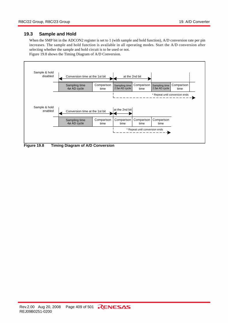
R8C/22 Group, R8C/23 Group 19. A/D Converter
Rev.2.00 Aug 20, 2008 Page 409 of 501REJ09B0251-0200
19.3 Sample and HoldWhen the SMP bit in the ADCON2 register is set to 1 (with sample and hold function), A/D conversion rate per pinincreases. The sample and hold function is available in all operating modes. Start the A/D conversion afterselecting whether the sample and hold circuit is to be used or not.Figure 19.8 shows the Timing Diagram of A/D Conversion.
Figure 19.8 Timing Diagram of A/D Conversion
Sampling time4ø AD cycle
Sample & holddisabled Conversion time at the 1st bit at the 2nd bit
Comparisontime
Sampling time2.5ø AD cycle
Comparisontime
Sampling time2.5ø AD cycle
Comparisontime
* Repeat until conversion ends
Sampling time4ø AD cycle
Sample & holdenabled Conversion time at the 1st bit at the 2nd bit
Comparisontime
Comparisontime
Comparisontime
* Repeat until conversion ends
Comparisontime

R8C/22 Group, R8C/23 Group 19. A/D Converter
Rev.2.00 Aug 20, 2008 Page 410 of 501REJ09B0251-0200
19.4 A/D Conversion CyclesFigure 19.9 shows the A/D Conversion Cycles.
Figure 19.9 A/D Conversion Cycles
A/D Conversion Mode
Without Sample & Hold
Without Sample & Hold
With Sample & Hold
With Sample & Hold
8 bits
10 bits
8 bits
10 bits
ConversionTime
ComparisonTime
ComparisonTime End processSampling
Time
End processConversion time at the 1st bit
SamplingTime
Conversion time at the 2ndbit and the follows
49φAD 4φAD 2.0φAD 2.5φAD 2.5φAD 8.0φAD
59φAD 4φAD 2.0φAD 2.5φAD 2.5φAD 8.0φAD
28φAD 4φAD 2.5φAD 0.0φAD 2.5φAD 4.0φAD
33φAD 4φAD 2.5φAD 0.0φAD 2.5φAD 4.0φAD

R8C/22 Group, R8C/23 Group 19. A/D Converter
Rev.2.00 Aug 20, 2008 Page 411 of 501REJ09B0251-0200
19.5 Internal Equivalent Circuit of Analog InputFigure 19.10 shows the Internal Equivalent Circuit of Analog Input.
Figure 19.10 Internal Equivalent Circuit of Analog Input
VCC
Parasitic Diode
Chopper-typeAmplifier
A/D SuccessiveConversion Register
Comparisonvoltage
b1b2 b0
VCC VSS
AN0
VSS
i = 12
AN11
VREF
AVSS
Vref
Comparison reference voltage(Vref) generator
SW1 SW2
AVCC
AMP
SW3
AVSS
VIN
SW4
SW5
SW1
Parasitic Diode ON ResistorApprox. 2kΩ Wiring Resistor
Approx. 0.2kΩ
ON ResistorApprox. 0.6kΩ
ON ResistorApprox. 2kΩ Wiring Resistor
Approx. 0.2kΩ
i Ladder-typeSwitches
A/D Control Register 0
ON ResistorApprox. 0.6k f
Analog InputVoltage
SamplingControl Signal
ON ResistorApprox. 5kΩ
C = Approx.1.5pF
A/D ConversionInterrupt Request
SW1 conducts only on the ports selected for analog input.
SW2 and SW3 are open when A/D conversion is not in progress;their status varies as shown by the waveforms in the diagrams on the left.
SW4 conducts only when A/D conversion is not in progress.
SW5 conducts when A/D conversion is Comparison.
Control signalfor SW2
Control signalfor SW3
Sampling Comparison
Connect to
Connect to
Connect to
Connect to
NOTE:1. Use only as a standard for designing this data.
Mass production may cause some changes in device characteristics.
i Ladder-typeWiring Resistors
Resistorladder
ReferenceControl Signal
b4

R8C/22 Group, R8C/23 Group 19. A/D Converter
Rev.2.00 Aug 20, 2008 Page 412 of 501REJ09B0251-0200
19.6 Output Impedance of Sensor Under A/D ConversionTo carry out A/D conversion properly, charging the internal capacitor C shown in Figure 19.11 has to be completedwithin a specified period of time. T (sampling time) as the specified time. Let output impedance of sensorequivalent circuit be R0, internal resistance of microcomputer be R, precision (error) of the A/D converter be X,and the resolution of A/D converter be Y (Y is 1024 in the 10-bit mode, and 256 in the 8-bit mode).
Figure 19.11 shows Analog Input Pin and External Sensor Equivalent Circuit. When the difference between VINand VC becomes 0.1LSB, we find impedance R0 when voltage between pins VC changes from 0 to VIN (0.1/1024)VIN in time T. (0.1/1024) means that A/D precision drop due to insufficient capacitor charge is held to 0.1LSB attime of A/D conversion in the 10-bit mode. Actual error however is the value of absolute precision added to0.1LSB.When f(XIN) = 10 MHz, T = 0.25 µs in the A/D conversion mode without sample & hold. Output impedance R0for sufficiently charging capacitor C within time T is determined as follows.
T = 0.25 µs, R = 2.8 kΩ, C = 6.0 pF, X = 0.1, and Y = 1024. Hence,
Thus, the allowable output impedance of the sensor equivalent circuit, making the precision (error) 0.1LSB or less,is approximately 1.7 kΩ maximum.
Figure 19.11 Analog Input Pin and External Sensor Equivalent Circuit
VC is generally VC = VIN 1 - e
And when t = T, VC = VIN - VIN = VIN 1 -
e =
= 1n
Hence, R0 = - -R
- t1C(R0 + R)
XY
XY
XY
XY
- T1C(R0 + R)
- T1C(R0 + R)
TC 1nX
Y
R0 = -6.0 × 10⁻¹² 1n
0.11024
0.25 × 10⁻⁶- 2.8 × 10³ 1.7 × 10³~~
MCU
Sensor equivalent circuit
R(2.8kΩ)
C(6.0pF)
R0
VIN
VC
NOTE:1. The capacity of the terminal is assumed to be 4.5 pF
R8C/22 Group, R8C/23 Group 19. A/D Converter
Rev.2.00 Aug 20, 2008 Page 413 of 501REJ09B0251-0200
19.7 Notes on A/D Converter• Write to each bit (other than bit 6) in the ADCON0 register, each bit in the ADCON1 register, or the SMP bit
in the ADCON2 register when the A/D conversion stops (before a trigger occurs).When the VCUT bit in the ADCON1 register is changed from 0 (VREF not connected) to 1 (VREFconnected), wait for at least 1 µs or longer before the A/D conversion starts.
• When changing A/D operating mode, select an analog input pin again.• When using in one-shot mode. Ensure that the A/D conversion is completed and read the AD register. The IR
bit in the ADIC register or the ADST bit in the ADCON0 register can determine whether the A/D conversionis completed.
• When using the repeat mode, select the frequency of the A/D converter operating clock φAD or more for theCPU clock during A/D conversion.Do not select the fOCO-F for the φAD.
• If setting the ADST bit in the ADCON0 register to 0 (A/D conversion stops) by a program and the A/Dconversion is forcibly terminated during the A/D conversion operation, the conversion result of the A/Dconverter will be indeterminate. If the ADST bit is set to 0 by a program, do not use the value of AD register.
• Connect 0.1 µF capacitor between the P4_2/VREF pin and AVSS pin.• Do not enter stop mode during A/D conversion.• Do not enter wait mode when the CM02 bit in the CM0 register is set to 1 (peripheral function clock stops in
wait mode) during A/D conversion.

R8C/22 Group, R8C/23 Group 20. Flash Memory
Rev.2.00 Aug 20, 2008 Page 414 of 501REJ09B0251-0200
20. Flash Memory
20.1 OverviewIn the flash memory version, rewrite operations to the flash memory can be performed in three modes; CPUrewrite, standard serial I/O, parallel I/O modes.Table 20.1 lists the Flash Memory Performance (see Table 1.1 and Table 1.2 Performance for the items not listedon Table 20.1).
NOTES:1. Definition of programming and erasure endurance
The programming and erasure endurance is defined on a per-block basis.If the programming and erasure endurance is n (n = 100 or 10,000), each block can be erased n times. For example, if 1,024 1-byte writes are performed to different addresses in block A, a 1-Kbyte block, and then the block is erased, the programming/erasure endurance still stands at one. When performing 100 or more rewrites, the actual erasure endurance can be reduced by executing programming operations in such a way that all blank areas are used before performing an erase operation. Avoid rewriting only particular blocks and try to average out the programming and erasure endurance of the blocks. It is also advisable to retain data on the erasure endurance of each block and limit the number of erase operations to a certain number.
2. Blocks A and B are embedded only in the R8C/23 Group.
Table 20.1 Flash Memory PerformanceItem Specification
Flash Memory Operating Mode 3 modes (CPU rewrite, standard serial I/O, and parallel I/O mode)Division of Erase Block See Figure 20.1 and Figure 20.2Program Method Byte unitErase Method Block eraseProgram, Erase Control Method Program and erase control by software commandRewrite Control Method Rewrite control for blocks 0 and 1 by FMR02 bit in FMR0 register
Rewrite control for block 0 by FMR16 bit and block 1 by FMR16 bitNumber of Commands 5 commandsProgramming and erase endurance(1)
Blocks 0 and 1 (Program ROM)
R8C/22 Group: 100 times; R8C/23 Group: 1,000 times
Blocks A and B (Data Flash)(2)
10,000 times
ID Code Check Function Standard serial I/O mode supportedROM Code Protect For parallel I/O mode supported

R8C/22 Group, R8C/23 Group 20. Flash Memory
Rev.2.00 Aug 20, 2008 Page 415 of 501REJ09B0251-0200
Table 20.2 Flash Memory Rewrite ModesFlash Memory Rewrite Mode CPU Rewrite Mode Standard Serial I/O Mode Parallel I/O Mode
Function User ROM area is rewritten by executing software commands from the CPU.EW0 mode: Rewritable in the
RAMEW1 mode: Rewritable in flash
memory
User ROM area is rewritten by using a dedicated serial programmer.
User ROM area is rewritten by using a dedicated parallel programmer.
Areas which can be rewritten
User ROM area User ROM area User ROM area
Operating mode Single chip mode Boot mode Parallel I/O modeROM programmer None Serial programmer Parallel programmer

R8C/22 Group, R8C/23 Group 20. Flash Memory
Rev.2.00 Aug 20, 2008 Page 416 of 501REJ09B0251-0200
20.2 Memory MapThe flash memory contains a user ROM area and a boot ROM area (reserved area).Figure 20.1 shows the Flash Memory Block Diagram for R8C/22 Group. Figure 20.2 shows the Flash MemoryBlock Diagram for R8C/23 Group.The user ROM area of R8C/23 Group contains an area which stores a MCU operating program (program ROM)and the 1-Kbyte block A and B (data flash).The user ROM area is divided into several blocks. The user ROM area can be rewritten in CPU rewrite andstandard serial I/O and parallel I/O modes.When rewriting the block 0 and block 1 in CPU rewrite mode, set the FMR02 bit in the FMR0 register to 1 (rewriteenables), and when setting the FMR15 bit in the FMR1 register to 0 (rewrite enables), block 0 is rewritable. Whensetting the FMR16 bit to 0 (rewrite enables), block 1 is rewritable.When rewriting the block 2 and block 3 in CPU rewrite mode, set the FMR02 bit in the FMR0 register to 1 (rewriteenables).The rewrite control program for standard serial I/O mode is stored in boot ROM area before shipment. The bootROM area and the user ROM area share the same address, but have an another memory.

R8C/22 Group, R8C/23 Group 20. Flash Memory
Rev.2.00 Aug 20, 2008 Page 417 of 501REJ09B0251-0200
Figure 20.1 Flash Memory Block Diagram for R8C/22 Group
User ROM area
Block 0: 32 Kbytes(1)
0C000h
13FFFh
64 Kbytes ROM product
0FFFFh10000h
0BFFFh
04000h
Block 1: 32 Kbytes(1)
User ROM area
Block 0: 32 Kbytes(1)
0C000h
13FFFh
96 Kbytes ROM product
0FFFFh10000h
0BFFFh
04000h
Block 1: 32 Kbytes(1)
Block 2: 32 Kbytes(2)
14000h
1BFFFh
User ROM area
Block 0: 32 Kbytes(1)
0C000h
13FFFh
128 Kbytes ROM product
0FFFFh10000h
0BFFFh
04000h
Block 1: 32 Kbytes(1)
Block 2: 32 Kbytes(2)
14000h
1BFFFh
Block 3: 32 Kbytes(2, 3)
1C000h
23FFFh
User ROM area
Block 0: 16 Kbytes(1)
0C000h
48 Kbytes ROM product
0FFFFh
0BFFFh
04000h
Block 1: 32 Kbytes(1)
User ROM area
Block 0: 16 Kbytes(1)
0C000h
32 Kbytes ROM product
0FFFFh
0BFFFh
08000h
Block 1: 16 Kbytes(1)
Program ROM
Boot ROM area (reserved area)(4)
8 Kbytes0E000h0FFFFh
NOTES:1. When setting the FMR02 bit in the FMR0 register to 1 (enables to rewrite) and the FMR15 bit in the FMR1 register to 0 (enable to rewrite),
Block 0 is rewritable. When setting the FMR16 bit to 0 (enables to rewrite), Block 1 is rewritable (only for CPU rewrite mode).2. When setting the FMR02 bit in the FMR0 register to 1 (enables to rewrite), Block 2 and Block 3 are rewritable (only for CPU rewrite mode).3. Do not use addresses 20000h to 23FFFh because these areas are used for the emulator debugger. Refer to 24. Notes on Emulator
Debugger.4. This area is to store the boot program provided by Renesas Technology.
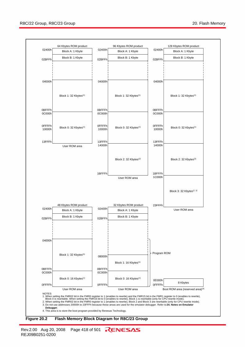
R8C/22 Group, R8C/23 Group 20. Flash Memory
Rev.2.00 Aug 20, 2008 Page 418 of 501REJ09B0251-0200
Figure 20.2 Flash Memory Block Diagram for R8C/23 Group
User ROM area
Block 0: 32 Kbytes(1)
0C000h
13FFFh
64 Kbytes ROM product
0FFFFh10000h
0BFFFh
04000h
Block 1: 32 Kbytes(1)
User ROM area
Block 0: 32 Kbytes(1)
0C000h
13FFFh
96 Kbytes ROM product
0FFFFh10000h
0BFFFh
04000h
Block 1: 32 Kbytes(1)
Block 2: 32 Kbytes(2)
14000h
1BFFFh
User ROM area
Block 0: 32 Kbytes(1)
0C000h
13FFFh
128 Kbytes ROM product
0FFFFh10000h
0BFFFh
04000h
Block 1: 32 Kbytes(1)
Block 2: 32 Kbytes(2)
14000h
1BFFFh
Block 3: 32 Kbytes(2, 3)
1C000h
23FFFh
User ROM area
Block 0: 16 Kbytes(1)
0C000h
48 Kbytes ROM product
0FFFFh
0BFFFh
04000h
Block 1: 32 Kbytes(1)
User ROM area
Block 0: 16 Kbytes(1)
0C000h
32 Kbytes ROM product
0FFFFh
0BFFFh
08000h
Block 1: 16 Kbytes(1)
Program ROM
Boot ROM area (reserved area)(4)
8 Kbytes0E000h0FFFFh
Block B: 1 Kbyte
Block A: 1 Kbyte02400h
02BFFh
Block B: 1 Kbyte
Block A: 1 Kbyte02400h
02BFFh Block B: 1 Kbyte
Block A: 1 Kbyte02400h
02BFFh
Block B: 1 Kbyte
Block A: 1 Kbyte02400h
02BFFh Block B: 1 Kbyte
Block A: 1 Kbyte02400h
02BFFh
NOTES:1. When setting the FMR02 bit in the FMR0 register to 1 (enables to rewrite) and the FMR15 bit in the FMR1 register to 0 (enables to rewrite),
Block 0 is rewritable. When setting the FMR16 bit to 0 (enables to rewrite), Block 1 is rewritable (only for CPU rewrite mode).2. When setting the FMR02 bit in the FMR0 register to 1 (enables to rewrite), Block 2 and Block 3 are rewritable (only for CPU rewrite mode).3. Do not use addresses 20000h to 23FFFh because these areas are used for the emulator debugger. Refer to 24. Notes on Emulator
Debugger.4. This area is to store the boot program provided by Renesas Technology.

R8C/22 Group, R8C/23 Group 20. Flash Memory
Rev.2.00 Aug 20, 2008 Page 419 of 501REJ09B0251-0200
20.3 Functions to Prevent Rewriting of Flash MemoryStandard serial I/O mode contains an ID code check function, and the parallel I/O mode contains a ROM codeprotect function to prevent the flash memory from reading or rewriting easily.
20.3.1 ID Code Check FunctionUse this function in standard serial I/O mode. Unless the flash memory is blank, the ID codes sent from theprogrammer and the ID codes written in the flash memory are determined whether they match. If the ID codesdo not match, the commands sent from the programmer are not acknowledged. The ID code consists of 8-bitdata, the areas of which, beginning with the first byte, are 00FFDFh, 00FFE3h, 00FFEBh, 00FFEFh, 00FFF3h,00FFF7h, and 00FFFBh. Write a program in which the ID codes are set at these addresses and write them in theflash memory.
Figure 20.3 Address for Stored ID Code
4 bytes
Address00FFDFh to 00FFDCh Undefined instruction vector
NOTE:1. The OFS register is assigned to 00FFFFh. Refer to
Figure 20.4 OFS Register for the OFS registerdetails.
Overflow vector00FFE3h to 00FFE0h
00FFE7h to 00FFE4h BRK instruction vectorAddress match vector00FFEBh to 00FFE8h
00FFEFh to 00FFEChOscillation stop detection/watchdogtimer/voltage monitor 2 vector00FFF3h to 00FFF0h
00FFF7h to 00FFF4h Address break00FFFBh to 00FFF8h
Reset vector00FFFFh to 00FFFCh
(Reserved)
ID1ID2
ID3ID4ID5ID6ID7(1)
Single step vector

R8C/22 Group, R8C/23 Group 20. Flash Memory
Rev.2.00 Aug 20, 2008 Page 420 of 501REJ09B0251-0200
20.3.2 ROM Code Protect FunctionThe ROM code protect function disables to read and change the internal flash memory by the OFS register inparallel I/O mode.Figure 20.4 shows the OFS Register.The ROM code protect function is enabled by writing 0 to the ROMCP1 bit and 1 to the ROMCR bit anddisables to read and change the internal flash memory. Once the ROM code protect is enabled, the content in the internal flash memory cannot be rewritten in parallelI/O mode. When the ROM code protect is disabled, erase the block including the OFS register with CPUrewrite mode or standard serial I/O mode.
Figure 20.4 OFS Register
Option Function Select Register(1)
Symbol Address Before ShipmentOFS 0FFFFh FFh(3)
Bit Symbol Bit Name Function RW
Reserved bit
NOTES:1.
2.3.
b7 b6 b5 b4 b3 b2 b1 b0
1 1 1
—(b1)
Set to 1RW
WDTONWatchdog timer startselect bit
0 : Starts w atchdog timer automatically after reset1 : Watchdog timer is inactive after reset RW
ROMCRROM code protectdisabled bit
0 : ROM code protect disabled1 : ROMCP1 enabled RW
ROMCP1ROM code protect bit 0 : ROM code protect enabled
1 : ROM code protect disabled RW
RW
—(b5-b4)
Reserved bits Set to 1RW
If the block including the OFS register is erased, FFh is set to the OFS register.To use the pow er-on reset, set the LVD1ON bit to 0 (voltage monitor 1 reset enabled after reset).
LVD1ONVoltage detection circuitstart bit(2)
0 : Voltage monitor 1 reset enabled after reset1 : Voltage monitor 1 reset disabled after reset RW
The OFS register is on the f lash memory. Write to the OFS register w ith a program. After w riting is completed, do notw rite additions to the OFS register.
CSPROINICount source protectmode after reset selectbit
0 : Count source protect mode enabled after reset1 : Count source protect mode disabled after reset

R8C/22 Group, R8C/23 Group 20. Flash Memory
Rev.2.00 Aug 20, 2008 Page 421 of 501REJ09B0251-0200
20.4 CPU Rewrite ModeIn CPU rewrite mode, user ROM area can be rewritten by executing software commands from the CPU. Therefore,the user ROM area can be rewritten directly while the MCU is mounted on a board without using such as a ROMprogrammer. Execute the program and block erase commands only to each block in user ROM area.When an interrupt request is generated during an erase operation in CPU rewrite mode, the flash module containsan erase-suspend function which performs the interrupt process after the erase operation is halted temporarily.During the erase-suspend, user ROM area can be read by a program.When an interrupt request is generated during the auto-program operation in CPU rewrite mode, the flash modulecontains a program-suspend function which performs the interrupt process after the auto-program operationsuspends. During the program-suspend, user ROM area can be read by a program.CPU rewrite mode contains erase write 0 mode (EW0 mode) and erase write 1 mode (EW1 mode).Table 20.3 lists the Differences between EW0 Mode and EW1 Mode.
NOTE:1. When setting the FMR02 bit in the FMR0 register to 1 (rewrite enables) and rewriting block 0 is enabled by
setting the FMR15 bit in the FMR1 register to 0 (rewrite enables). Rewriting block 1 is enabled by setting the FMR16 bit to 0 (rewrite enables).
Table 20.3 Differences between EW0 Mode and EW1 ModeItem EW0 Mode EW1 Mode
Operating Mode Single chip mode Single chip modeAreas in which a Rewrite Control Program Can be Located
User ROM area User ROM area
Areas in which a Rewrite Control Program can be Executed
Necessary to transfer to any areas other than the flash memory (e.g., RAM) before executing
Executing directly in user ROM or RAM area possible
Areas which can be Rewritten
User ROM area User ROM areaHowever, other than the blocks which contain a rewrite control program(1)
Software Command Restriction
None • Program and block erase commandsCannot be run on any block which contains a rewrite control program
• Read status register commandCannot be executed
Modes After Program or Erase
Read status register mode Read array mode
Modes After Read Status Register
Read status register mode Do not execute this command
CPU Status During Auto- write and Auto-erase
Operating Hold state (I/O ports hold state before the command is executed)
Flash Memory Status Detection
• Read the FMR00, FMR06, and FMR07 bits in the FMR0 register by a program
• Execute the read status register command and read the SR7, SR5, and SR4 bits in the status register.
Read the FMR00, FMR06, and FMR07 bits in the FMR0 register by a program
Conditions for Transition to Erase-suspend
Set the FMR40 and FMR41 bits in the FMR4 register to 1 by a program.
The FMR40 bit in the FMR4 register is set to 1 and the interrupt request of the enabled maskable interrupt is generated
Conditions for Transitions to Program-suspend
Set the FMR40 and FMR42 bits in the FMR4 register to 1 by a program.
The FMR40 bit in the FMR4 register is set to 1 and the interrupt request of the enabled maskable interrupt is generated
CPU Clock 5 MHz or below No restriction to the following (clock frequency to be used)

R8C/22 Group, R8C/23 Group 20. Flash Memory
Rev.2.00 Aug 20, 2008 Page 422 of 501REJ09B0251-0200
20.4.1 EW0 ModeThe MCU enters CPU rewrite mode and software commands can be acknowledged by setting the FMR01 bit inthe FMR0 register to 1 (CPU rewrite mode enabled). In this case, since the FMR11 bit in the FMR1 register isset to 0, EW0 mode is selected.Use software commands to control a program and erase operations. The FMR0 register or the status register candetermine status when program and erase operation complete. When entering an erase-suspend, set the FMR40 bit to 1 (enables suspend) and the FMR41 bit to 1 (requestserase-suspend). Wait for td(SR-SUS) and ensure that the FMR46 bit is set to 1 (enables reading) beforeaccessing the user ROM area. The auto-erase operation restarts by setting the FMR41 bit to 0 (erase restarts).When entering a program-suspend during the auto-program, set the FMR40 bit to 1 (enables suspend) and theFMR42 bit to 1 (requests program-suspend). Wait for td(SR-SUS) and ensure that the FMR46 bit is set to 1(enables reading) before accessing the user ROM area. The auto-program operation restarts by setting theFMR42 bit to 0 (program restarts).
20.4.2 EW1 ModeThe MCU enters EW1 mode by setting the FMR11 bit to 1 (EW1 mode) after setting the FMR01 bit to 1 (CPUrewrite mode enabled).The FMR0 register can determine status when program and erase operation complete. Do not executecommands of the read status register in EW1 mode.To enable the erase-suspend function during the auto-erase, execute the block erase command after setting theFMR40 bit to 1 (enables suspend). The interrupt to enter an erase-suspend should be in interrupt enabled status.After passing td(SR-SUS) since the block erase command is executed, an interrupt request is acknowledged.When an interrupt request is generated, the FMR41 bit is automatically set to 1 (requests erase-suspend) and theauto-erase operation is halted. If the auto-erase operation does not complete (FMR00 bit is 0) when the interruptprocess completes, the auto-erase operation restarts by setting the FMR41 bit to 0 (erase restarts)To enable the program-suspend function during the auto-program, execute the program command after settingthe FMR40 bit to 1 (enables suspend). The interrupt to enter a program-suspend should be in interrupt enabledstatus. After waiting for td(SR-SUS) since the program command is executed, an interrupt request isacknowledged.When an interrupt request is generated, the FMR42 bit is automatically set to 1 (requests program-suspend) andthe auto-program operation suspends. When the auto-program operation does not complete (FMR00 bit is 0)after the interrupt process completes, the auto-program operation restarts by setting the FMR42 bit to 0(program restarts).

R8C/22 Group, R8C/23 Group 20. Flash Memory
Rev.2.00 Aug 20, 2008 Page 423 of 501REJ09B0251-0200
Figure 20.5 shows the FMR0 Register, Figure 20.6 shows the FMR1 Register and Figure 20.7 shows the FMR4Register.
20.4.2.1 FMR00 BitThis bit indicates the operating status of the flash memory. The bit is 0 during programming, erasing (includingsuspend periods), or erase-suspend mode; otherwise, the bit is 1.
20.4.2.2 FMR01 BitThe MCU is made ready to accept commands by setting the FMR01 bit to 1 (CPU rewrite mode).
20.4.2.3 FMR02 BitThe block0, block1, block2 and block3 do not accept the program and block erase commands if the FMR02 bitis set to 0 (rewrite disabled).The block0 and block1 are controlled rewriting in the FMR15 and FMR16 bits if the FMR02 bit is set to 1(rewrite enabled).
20.4.2.4 FMSTP BitThis bit is provided for initializing the flash memory control circuits, as well as for reducing the amount ofcurrent consumed in the flash memory. The flash memory is disabled against access by setting the FMSTP bit to1. Therefore, the FMSTP bit must be written to by a program transferred to the RAM.In the following cases, set the FMSTP bit to 1:
• When flash memory access resulted in an error while erasing or programming in EW0 mode (FMR00 bitnot reset to 1 (ready))
• When entering high-speed on-chip oscillator mode, low-speed on-chip oscillator mode (XIN clock stop) Figure 20.11 shows a Process to Reduce Power Consumption in High-Speed On-Chip Oscillator Mode, Low-Speed On-Chip Oscillator Mode (XIN Clock Stops) and Low-Speed Clock Mode (XIN Clock Stops). Note thatwhen going to stop or wait mode while the CPU rewrite mode is disabled, the FMR0 register does not need tobe set because the power for the flash memory is automatically turned off and is turned back on again afterreturning from stop or wait mode.
20.4.2.5 FMR06 BitThis is a read-only bit indicating the status of auto program operation. The bit is set to 1 when a program erroroccurs; otherwise, it is cleared to 0. For details, refer to the description of the 20.4.5 Full Status Check.
20.4.2.6 FMR07 BitThis is a read-only bit indicating the status of auto erase operation. The bit is set to 1 when an erase error occurs;otherwise, it is set to 0. Refer to 20.4.5 Full Status Check for the details.
20.4.2.7 FMR11 BitSetting this bit to 1 (EW1 mode) places the MCU in EW1 mode.
20.4.2.8 FMR15 BitWhen the FMR02 bit is set to 1 (rewrite enabled) and the FMR15 bit is set to 0 (rewrite enabled), the block0accepts the program command and block erase command.
20.4.2.9 FMR16 BitWhen the FMR02 bit is set to 1 (rewrite enabled) and the FMR16 bit is set to 0 (rewrite enabled), the block1accepts the program command and block erase command.
20.4.2.10 FMR40 BitThe suspend function is enabled by setting the FMR40 bit to 1 (enable).

R8C/22 Group, R8C/23 Group 20. Flash Memory
Rev.2.00 Aug 20, 2008 Page 424 of 501REJ09B0251-0200
20.4.2.11 FMR41 BitIn EW0 mode, the MCU enters erase-suspend mode when setting the FMR41 bit to 1 by a program. TheFMR41 bit is automatically set to 1 (requests erase-suspend) when an interrupt request of an enabled interrupt isgenerated in EW1 mode, and then the MCU enters erase-suspend mode.Set the FMR41 bit to 0 (erase restart) when the auto-erase operation restarts.
20.4.2.12 FMR42 BitIn EW0 mode, the MCU enters program-suspend mode when setting the FMR42 bit to 1 by a program. TheFMR42 bit is automatically set to 1 (requests program-suspend) when an interrupt request of an enabledinterrupt is generated in EW1 mode, and then the MCU enters program-suspend mode. Set the FMR42 bit to 0 (program restarts) when the auto-program operation restarts.
20.4.2.13 FMR43 BitWhen the auto-erase operation starts, the FMR43 bit is set to 1 (during erase execution). The FMR43 bitremains 1 (during erase execution) during erase-suspend operation.When the auto-erase operation ends, the FMR43 bit is set to 0 (erase not executed).
20.4.2.14 FMR44 BitWhen the auto-program starts, the FMR44 bit is set to 1 (during program execution). The FMR44 bit remains 1(during program execution) during program-suspend operation.When the auto-program operation ends, the FMR44 bit is set to 0 (program not executed).
20.4.2.15 FMR46 BitThe FMR46 bit is set to 0 (reading disabled) during auto-program or auto-erase execution and set to 1 (readingenabled) in suspend mode. Do not access the flash memory while this bit is set to 0.
20.4.2.16 FMR47 BitPower consumption when reading the flash memory can be reduced by setting the FMR47 bit to 1 (enabled) inlow-speed on-chip oscillator mode (XIN clock stops).

R8C/22 Group, R8C/23 Group 20. Flash Memory
Rev.2.00 Aug 20, 2008 Page 425 of 501REJ09B0251-0200
Figure 20.5 FMR0 Register
Flash Memory Control Register 0
Symbol Address After ResetFMR0 01B7h 00000001b
Bit Symbol Bit Name Function RWRY/BY
____ status f lag
NOTES:1.
2.
3.4.5.
6.
FMR07
b3 b2 b1 b0
—(b5-b4)
FMR00
FMSTP
FMR020 : Disables rew rite1 : Enables rew rite
Flash memory stop bit(3,5) 0 : Enables f lash memory operation1 : Stops f lash memory (Enters low -pow er consumption state and f lash memory is reset)
FMR01
Block 0, 1, 2, 3 rew rite enablebit(2,6)
0 : Busy (During w riting or erasing)1 : Ready
CPU rew rite mode select bit(1)
b7 b6 b5 b4
RO
0 0
Reserved bit Set to 0
RW
0 : Completed successfully1 : Terminated by error
RW
RO
RO
RW
RW
0 : CPU rew rite mode disabled1 : CPU rew rite mode enabled
When setting the FMR01 bit to 0 (CPU rew rite mode disabled), the FMR02 bit is set to 0 (disables rew rite).
This bit is set to 0 by executing the clear status command.This bit is enabled w hen the FMR01 bit is set to 1 (CPU rew rite mode enabled). When the FMR01 bit is set to 0 andw riting 1 to the FMSTP bit, the FMSTP bit is set to 1. The f lash memory does not enter low -pow er consumption stat
FMR06
When setting this bit to 1, set to 1 immediately after setting it f irst to 0. Do not generate an interrupt betw een settingthe bit to 0 and setting it to 1. Enter read array mode and set this bit to 0.Set this bit to 1 immediately after setting this bit f irst to 0 w hile the FMR01 bit is set to 1.Do not generate an interrupt betw een setting the bit to 0 and setting it to 1.Set this bit by a program transferred to the RAM.
Program status f lag(4) 0 : Completed successfully1 : Terminated by error
Erase status f lag(4)

R8C/22 Group, R8C/23 Group 20. Flash Memory
Rev.2.00 Aug 20, 2008 Page 426 of 501REJ09B0251-0200
Figure 20.6 FMR1 Register
Flash Memory Control Register 1
Symbol Address After ResetFMR1 01B5h 1000000Xb
Bit Symbol Bit Name Function RW
NOTES:1.
2.3.
b3 b2
Set to 0
0b1 b0
FMR11
—(b4-b2)
1 0b7 b6 b5 b4
RW
FMR15
—(b0)
Reserved bit
When read, its content is indeterminate.
EW1 mode select bit(1,2) 0 : EW0 mode1 : EW1 mode
Block 0 rew rite disable bit(2,3) 0 : Enables rew rite1 : Disables rew rite
When the FMR01 bit is set to 1 (CPU rew rite mode enabled), the FMR15 and FMR16 bits can be w ritten.When setting this bit to 0, set to 0 immediately after setting it f irst to 1.When setting this bit to 1, set it to 1.
—(b7)
0
RW
RW
RW
RO
RW
Reserved bit
0 : Enables rew rite1 : Disables rew riteFMR16
Block 1 rew rite disable bit(2,3)
When setting this bit to 1, set to 1 immediately after setting it f irst to 0 w hile the FMR01 bit is set to 1 (CPU rew ritemode enable) . Do not generate an interrupt betw een setting the bit to 0 and setting it to 1.This bit is set to 0 by setting the FMR01 bit to 0 (CPU rew rite mode disabled).
Reserved bit Set to 1

R8C/22 Group, R8C/23 Group 20. Flash Memory
Rev.2.00 Aug 20, 2008 Page 427 of 501REJ09B0251-0200
Figure 20.7 FMR4 Register
Flash Memory Control Register 4
Symbol Address After ResetFMR4 01B3h 01000000b
Bit Symbol Bit Name Function RW
NOTES:1.
2.
3.
4.5.
When setting this bit to 1, set to 1 immediately after setting it f irst to 0. Do not generate an interrupt betw een settingthe bit to 0 and setting it to 1.This bit is enabled w hen the FMR40 bit is set to 1 (enable) and this bit can be w ritten during the period betw eenissuing an erase command and completing an erase (This bit is set to 0 during the periods other than above.)In EW0 mode, this can be set to 0 or 1 by a program.In EW1 mode, this bit is automatically set to 1 if a maskable interrupt is generated during an erase operation w hile theFMR40 bit is set to 1. Do not set this bit to 1 by a program (0 can be w ritten).
b3 b2
Set to 0
b1 b0
FMR41
—(b5-b2)
0
FMR40
FMR42
FMR44
b7 b6 b5 b4
RW
RW
Erase-suspend functionenable bit(1)
0 : Disables reading1 : Enables reading
Reserved bit
0 : Disable1 : Enable
Erase-suspend request bit(2) 0 : Erase restart1 : Erase-suspend request
RO
RO
RW
FMR43Erase command f lag 0 : Erase not executed
1 : During erase execution RO
0 : Disable1 : Enable
FMR46
Program-suspend request bit(3) 0 : Program restart1 : Program-suspend request
Set the FMR01 bit in the FMR0 register to 0 (CPU rew rite mode disabled) in low -pow er-consumption read mode.In high-speed clock mode and high-speed on-chip oscillator mode, set the FMR47 bit to 0 (disabled).
Program command f lag 0 : Program not executed1 : During program execution RO
The FMR42 bit is enabled only w hen the FMR40 bit is set to 1 (enable) and programming to the FMR42 bit is enableduntil the auto-program ends since the program command is generated. (This bit is set to 0 during periods other thanabove.)In EW0 mode, 0 or 1 can be programmed to the FMR42 bit by a program.In EW1 mode, the FMR42 bit is automatically set to 1 by generating a maskable interrupt during the auto-programw hen the FMR40 bit is set to 1. 1 cannot be programmed to the FMR42 bit by a program.
FMR47
Read status f lag
RWLow -pow er consumption readmode enable bit (1,4)

R8C/22 Group, R8C/23 Group 20. Flash Memory
Rev.2.00 Aug 20, 2008 Page 428 of 501REJ09B0251-0200
Figure 20.8 shows the Timing of Suspend Operation.
Figure 20.8 Timing of Suspend Operation
Erasestarts
Erasesuspends
FMR00 bit inFMR0 register
Programstarts
Programsuspends
Programrestarts
Programends
During erase During program During program
Eraserestarts
Eraseends
During erase
FMR46 bit inFMR4 register
FMR44 bit inFMR4 register
FMR43 bit inFMR4 register
1
0
1
0
1
0
1
0
Check that theFMR43 bit is set to 1(during eraseexecution), and thatthe erase operationhas not ended.
Check that theFMR44 bit is set to 1(during programexecution), and thatthe program has notended.
Check the status,and that theprogram endsnormally.
Check the status,and that the eraseoperation endsnormally.
Remains 0 during suspend
Remains 1 during suspend
The above figure shows an example of the use of program-suspend during programming following erase-suspend.
NOTE:1. If program-suspend is entered during erase-suspend, always restart programming.
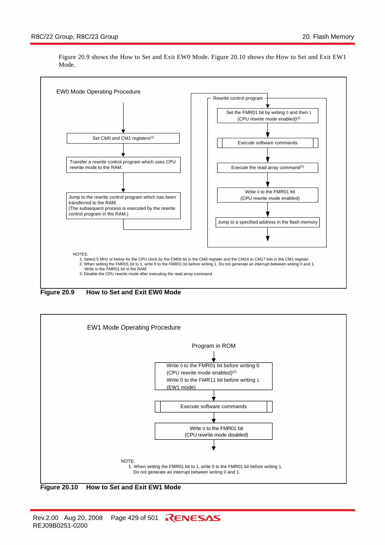
R8C/22 Group, R8C/23 Group 20. Flash Memory
Rev.2.00 Aug 20, 2008 Page 429 of 501REJ09B0251-0200
Figure 20.9 shows the How to Set and Exit EW0 Mode. Figure 20.10 shows the How to Set and Exit EW1Mode.
Figure 20.9 How to Set and Exit EW0 Mode
Figure 20.10 How to Set and Exit EW1 Mode
Set CM0 and CM1 registers(1)
Set the FMR01 bit by writing 0 and then 1(CPU rewrite mode enabled)(2)
Execute the read array command(3)
Execute software commands
Write 0 to the FMR01 bit(CPU rewrite mode enabled)
Jump to a specified address in the flash memory
Rewrite control program
NOTES:1. Select 5 MHz or below for the CPU clock by the CM06 bit in the CM0 register and the CM16 to CM17 bits in the CM1 register.2. When setting the FMR01 bit to 1, write 0 to the FMR01 bit before writing 1. Do not generate an interrupt between writing 0 and 1.
Write to the FMR01 bit in the RAM.3. Disable the CPU rewrite mode after executing the read array command.
EW0 Mode Operating Procedure
Transfer a rewrite control program which uses CPUrewrite mode to the RAM.
Jump to the rewrite control program which has beentransferred to the RAM.(The subsequent process is executed by the rewritecontrol program in the RAM.)
Write 0 to the FMR01 bit before writing 0(CPU rewrite mode enabled)(1)
Write 0 to the FMR11 bit before writing 1(EW1 mode)
Execute software commands
Write 0 to the FMR01 bit(CPU rewrite mode disabled)
NOTE:1. When setting the FMR01 bit to 1, write 0 to the FMR01 bit before writing 1. Do not generate an interrupt between writing 0 and 1.
EW1 Mode Operating Procedure
Program in ROM

R8C/22 Group, R8C/23 Group 20. Flash Memory
Rev.2.00 Aug 20, 2008 Page 430 of 501REJ09B0251-0200
Figure 20.11 Process to Reduce Power Consumption in High-Speed On-Chip Oscillator Mode, Low-Speed On-Chip Oscillator Mode (XIN Clock Stops) and Low-Speed Clock Mode (XIN Clock Stops)
Transfer a high-speed on-chip oscillator mode, low-speed on-chip oscillator mode (XIN clock stops)program to the RAM
Jump to the high-speed on-chip oscillator mode, low-speed on-chip oscillator mode (XIN clock stops) programwhich has been transferred to the RAM.(The subsequent processing is executed by a program inthe RAM.)
Write 0 to the FMR01 bit before writing 1 (CPU rewrite mode enabled)
Switch the clock source for the CPU clock.Turn XIN off
Process in high-speed on-chip oscillatormode, low-speed on-chip oscillator mode(XIN clock stops)
Write 0 to the FMR01 bit(CPU rewrite mode disabled)
Jump to a specified address in the flash memory
High-speed on-chip oscillatormode, low-speed on-chiposcillator mode (XIN clock stops)program
NOTES:1. Set the FMR01 bit to 1 (CPU rewrite mode enabled) before setting the FMSTP bit to 1 .2. Before the clock source for CPU clock can be changed, the clock to which to be changed must be stable.3. Insert a 30 µs wait time in a program. Do not access to the flash memory during this wait time.
Write 1 to the FMSTP bit (Flash memory stops.Low power consumption state)(1)
Wait until the flash memory circuit stabilizes(30 µs)(3)
Write 0 to the FMSTP bit(flash memory operation)
Turn XIN clock on→wait unti l oscil lationstabilizes→switch the clock source for CPUclock(2)

R8C/22 Group, R8C/23 Group 20. Flash Memory
Rev.2.00 Aug 20, 2008 Page 431 of 501REJ09B0251-0200
20.4.3 Software CommandsSoftware commands are described below. Read or write commands and data from or to in 8-bit units.
SRD: Status register data (D7 to D0)WA: Write address (Ensure the address specified in the first bus cycle is the same address as the write
address specified in the second bus cycle.)WD: Write data (8 bits)BA: Given block address×: Any specified address in the user ROM area
20.4.3.1 Read Array CommandThe read array command reads the flash memory.The MCU enters read array mode by writing FFh in the first bus cycle. If entering the read address after thefollowing bus cycles, the content of the specified address can be read in 8-bit units.Since the MCU remains in read array mode until another command is written, the contents of multipleaddresses can be read continuously.In addition, the MCU enters read array mode after a reset.
20.4.3.2 Read Status Register CommandThe read status register command reads the status register.If writing 70h in the first bus cycle, the status register can be read in the second bus cycle. (Refer to 20.4.4Status Registers) When reading the status register, specify an address in the user ROM area.Do not execute this command in EW1 mode.The MCU remains in read status register mode until the next read array command is written.
20.4.3.3 Clear Status Register CommandThe clear status register command sets the status register to 0.If writing 50h in the first bus cycle, the FMR06 to FMR07 bits in the FMR0 register and SR4 to SR5 in thestatus register will be set to 0.
Table 20.4 Software Commands
CommandFirst Bus Cycle Second Bus Cycle
Mode Address Data(D7 to D0) Mode Address Data
(D7 to D0)Read Array Write × FFhRead Status Register Write × 70h Read × SRDClear Status Register Write × 50hProgram Write WA 40h Write WA WDBlock Erase Write × 20h Write BA D0h

R8C/22 Group, R8C/23 Group 20. Flash Memory
Rev.2.00 Aug 20, 2008 Page 432 of 501REJ09B0251-0200
20.4.3.4 Program CommandThe program command writes data to the flash memory in 1-byte units.By writing 40h in the first bus cycle and data in the second bus cycle to the write address, and an auto programoperation (data program and verify) will start. Make sure the address value specified in the first bus cycle is thesame address as the write address specified in the second bus cycle.The FMR00 bit in the FMR0 register can determine whether auto programming has completed.When suspend function disabled, the FMR00 bit is set to 0 during auto-programming and set to 1 when auto-programming completes.When suspend function enabled, the FMR44 bit is set to 1 during auto-programming and set to 0 when auto-programming completes.The FMR06 bit in the FMR0 register can determine the result of auto programming after it has been finished.(Refer to 20.4.5 Full Status Check)When the FMR02 bit in the FMR0 register is set to 0 (disable rewriting), program commands targeting block 0to 3 are not acknowledged. When the FMR02 bit is set to 1 (rewrite enables) and the FMR15 bit in the FMR1register is set to 1 (disable rewriting), program commands targeting block 0 are not acknowledged. When theFMR16 bit is set to 1 (disable rewriting), program commands targeting block 1 are not acknowledged.Figure 20.12 shows the Program Command (When Suspend Function Disabled). Figure 20.13 shows theProgram Command (When Suspend Function Enabled).In EW1 mode, do not execute this command on any address at which the rewrite control program is allocated.In EW0 mode, the MCU enters read status register mode at the same time auto programming starts and thestatus register can be read. The status register bit 7 (SR7) is set to 0 at the same time auto programming startsand set back to 1 when auto programming completes. In this case, the MCU remains in read status registermode until a read array command is written next. Reading the status register can determine the result of autoprogramming after auto programming has completed.
Figure 20.12 Program Command (When Suspend Function Disabled)
Start
Write the command code 40h tothe write address
Write data to the write address
FMR00 = 1?
Full status check
Program completed
No
Yes

R8C/22 Group, R8C/23 Group 20. Flash Memory
Rev.2.00 Aug 20, 2008 Page 433 of 501REJ09B0251-0200
Figure 20.13 Program Command (When Suspend Function Enabled)
Start
Write the command code 40hto the write address
Write data to the write address
FMR44 = 0 ?
Full status check
Program completed
No
Yes
EW0 Mode
FMR40 = 1
Start
Write the command code 40h
Write data to the write address
FMR44 = 0 ?
Full status check
Program completed
No
Yes
EW1 Mode
FMR40 = 1
Maskable interrupt (2)
REIT
Access flash memory
FMR42 = 0
NOTES:1. In EW0 mode, the interrupt vector table and interrupt routine for interrupts to be used should be allocated to the RAM area.2. td(SR-SUS) is needed until the interrupt request is acknowledged after it is generated. The interrupt to enter suspend
should be in interrupt enabled status.3. When no interrupt is used, the instruction to enable interrupts is not needed.4. td(SR-SUS) is needed until program is suspended after the FMR42 bit in the FMR4 register is set to 1.
Maskable interrupt(1)
FMR46 = 1 ?
REIT
Yes
FMR42 = 1(4)
FMR42 = 0
Access flash memory
FMR44 = 1 ?
Yes
No
Access flash memory
No
I = 1 (enable interrupt)
I = 1 (enable interrupt)(3)

R8C/22 Group, R8C/23 Group 20. Flash Memory
Rev.2.00 Aug 20, 2008 Page 434 of 501REJ09B0251-0200
20.4.3.5 Block EraseIf writing 20h in the first bus cycle and D0h to the given address of a block in the second bus cycle, and an autoerase operation (erase and verify) will start.The FMR00 bit in the FMR0 register can determine whether auto erasing has completed.The FMR00 bit is set to 0 during auto erasing and set to 1 when auto erasing completes.The FMR07 bit in the FMR0 register can determine the result of auto erasing after auto erasing has completed.(Refer to 20.4.5 Full Status Check)When the FMR02 bit in the FMR0 register is set to 0 (disable rewriting) or the FMR02 bit is set to 1 (rewriteenables) and the FMR15 bit in the FMR1 register is set to 1 (disable rewriting), the block erase command onblock 0 is not acknowledged. When the FMR16 bit is set to 1 (disable rewriting), the block erase command onblock 1 is not acknowledged.Do not use the block erase command during program-suspend.Figure 20.14 shows the Block Erase Command (When Erase-Suspend Function Disabled). Figure 20.15 showsthe Block Erase Command (When Erase-Suspend Function Enabled).In EW1 mode, do not execute this command on any address at which the rewrite control program is allocated.In EW0 mode, the MCU enters read status register mode at the same time auto erasing starts and the statusregister can be read. The status register bit 7 (SR7) is set to 0 at the same time auto erasing starts and set back to1 when auto erasing completes. In this case, the MCU remains in read status register mode until the read arraycommand is written next.
Figure 20.14 Block Erase Command (When Erase-Suspend Function Disabled)
Start
Write the command code 20h
Write ‘D0h’ to the given blockaddress
FMR00 = 1?
Full status check
Block erase completed
No
Yes

R8C/22 Group, R8C/23 Group 20. Flash Memory
Rev.2.00 Aug 20, 2008 Page 435 of 501REJ09B0251-0200
Figure 20.15 Block Erase Command (When Erase-Suspend Function Enabled)
Start
Write the command code 20h
Write D0h to any blockaddress
FMR00 = 1 ?
Full status check
Block erase completed
No
Yes
EW0 Mode
FMR40 = 1
Start
Write the command code 20h
Write D0h to any blockaddress
FMR00 = 1 ?
Full status check
Block erase completed
No
Yes
EW1 Mode
I = 1 (enable interrupt)
Maskable interrupt (2)
REIT
Access flash memory
FMR41 = 0
NOTES:1. In EW0 mode, the interrupt vector table and interrupt routine for interrupts to be used should be allocated to the RAM area.2. td(SR-SUS) is needed until the interrupt request is acknowledged after it is generated. The interrupt to enter suspend
should be in interrupt enabled status.3. When no interrupt is used, the instruction to enable interrupts is not needed.4. td(SR-SUS) is needed until erase is suspended after the FMR41 bit in the FMR4 register is set to 1.
Maskable interrupt(1)
FMR46 = 1 ?
REIT
Yes
FMR41 = 1(4)
FMR41 = 0
Access flash memory
FMR43 = 1 ?
Yes
No
Access flash memory
No
I = 1 (enable interrupt)(3)
FMR40 = 1

R8C/22 Group, R8C/23 Group 20. Flash Memory
Rev.2.00 Aug 20, 2008 Page 436 of 501REJ09B0251-0200
20.4.4 Status RegistersThe status register indicates the operating status of the flash memory and whether an erasing or programmingoperation completes normally or in error. Status of the status register can be read by the FMR00, FMR06, andFMR07 bits in the FMR0 register.Table 20.5 lists the Status Register Bits.In EW0 mode, the status register can be read in the following cases:
• When a given address in the user ROM area is read after writing the read status register command• When a given address in the user ROM area is read after executing the program or block erase command
but before executing the read array command.
20.4.4.1 Sequencer Status (Bits SR7 and FMR00)The sequencer status indicates operating status of the flash memory. SR7 = 0 (busy) during auto programmingand auto erasing, and is set to 1 (ready) at the same time the operation completes.
20.4.4.2 Erase Status (Bits SR5 and FMR07)Refer to 20.4.5 Full Status Check.
20.4.4.3 Program Status (Bits SR4 and FMR06)Refer to 20.4.5 Full Status Check.
• D0 to D7: Indicates the data bus which is read when the read status register command is executed.• The FMR07 (SR5) to FMR06 bits (SR4) are set to 0 by executing the clear status register command.• When the FMR07 bit (SR5) or FMR06 bit (SR4) is set to 1, the program and block erase command
cannot be accepted.
Table 20.5 Status Register BitsStatus
RegisterBit
FMR0Register
BitStatus Name
Description Valueafter
Reset0 1
SR0 (D0) − Reserved − − −SR1 (D1) − Reserved − − −SR2 (D2) − Reserved − − −SR3 (D3) − Reserved − − −SR4 (D4) FMR06 Program status Completed
normallyError 0
SR5 (D5) FMR07 Erase status Completed normally
Error 0
SR6 (D6) − Reserved − − −SR7 (D7) FMR00 Sequencer
statusBusy Ready 1

R8C/22 Group, R8C/23 Group 20. Flash Memory
Rev.2.00 Aug 20, 2008 Page 437 of 501REJ09B0251-0200
20.4.5 Full Status CheckWhen an error occurs, the FMR06 to FMR07 bits in the FMR0 register are set to 1, indicating occurrence ofeach specific error. Therefore, checking these status bits (full status check) can determine the executed result. Table 20.6 lists the Errors and FMR0 Register Status. Figure 20.16 shows the Full Status Check and HandlingProcedure for Individual Errors.
NOTE:1. The MCU enters read array mode by writing FFh in the second bus cycle of these commands, at the
same time the command code written in the first bus cycle will disabled.
Table 20.6 Errors and FMR0 Register StatusFMR0 Register (Status
Register) Status Error Error Occurrence ConditionFMR07(SR5) FMR06(SR4)
1 1 Command sequenceerror
• When any command is not written correctly• When invalid data other than those that can be written
in the second bus cycle of the block erase command is written (i.e., other than D0h or FFh)(1)
• When executing the program command or block erase command while rewriting is disabled using the FMR02 bit in the FMR0 register, the FMR15 or FMR16 bit in the FMR1 register.
• When inputting and erasing the address in which the Flash memory is not allocated during the erase command input
• When executing to erase the block which disables rewriting during the erase command input.
• When inputting and writing the address in which the Flash memory is not allocated during the write command input.
• When executing to write the block which disables rewriting during the write command input.
1 0 Erase error • When the block erase command is executed but not automatically erased correctly
0 1 Program error • When the program command is executed but not automatically programmed correctly.

R8C/22 Group, R8C/23 Group 20. Flash Memory
Rev.2.00 Aug 20, 2008 Page 438 of 501REJ09B0251-0200
Figure 20.16 Full Status Check and Handling Procedure for Individual Errors
NOTE: 1. To rewrite to the address where the program error occurs, check if the full
status check is complete normally and write to the address after the blockerase command is executed.
Full status check
FMR06 = 1and
FMR07 = 1?
FMR07 = 1?
FMR06 = 1?
Full status check completed
No
Yes
Yes
No
Yes
No
Command sequence error
Erase error
Program error
Command sequence error
Execute the clear status register command (set these status flags to 0)
Check if command is properly input
Re-execute the command
Erase error
Execute the clear status register command(set these status flags to 0)
Erase commandre-execution times ≤ 3 times?
Re-execute block erase command
Program error
Execute the clear status registercommand
(set these status flags to 0)
Specify the other address besides thewrite address where the error occurs for
the program address(1)
Re-execute program command
Block targeting for erasurecannot be used
No
Yes

R8C/22 Group, R8C/23 Group 20. Flash Memory
Rev.2.00 Aug 20, 2008 Page 439 of 501REJ09B0251-0200
20.5 Standard Serial I/O ModeIn standard serial I/O mode, the user ROM area can be rewritten while the MCU is mounted on-board by using aserial programmer which is applicable for the MCU.
There are three types of Standard serial I/O modes:• Standard serial I/O mode 1 . . . . Clock synchronous serial I/O used to connect with a serial programmer• Standard serial I/O mode 2 . . . . Clock asynchronous serial I/O used to connect with a serial programmer• Standard serial I/O mode 3 . . . . Special clock asynchronous serial I/O used to connect with a serial programmer
This MCU uses Standard serial I/O mode 2 and Standard serial I/O mode 3.
Refer to Appendix 2. Connection Examples between Serial Writer and On-Chip Debugging Emulator.Contact the manufacturer of your serial programmer for serial programmer. Refer to the user’s manual of yourserial programmer for details on how to use it.
Table 20.7 lists the Pin Functions (Flash Memory Standard Serial I/O Mode 2), Table 20.8 lists the Pin Functions(Flash Memory Standard Serial I/O Mode 3), Figure 20.17 shows Pin Connections for Standard Serial I/O Mode 3.After processing the pins shown in Table 20.8 and rewriting a flash memory using a writer, apply “H” to the MODEpin and reset a hardware if a program is operated on the flash memory in single-chip mode.
20.5.1 ID Code Check FunctionThe ID code check function determines whether the ID codes sent from the serial programmer and those writtenin the flash memory match (refer to 20.3 Functions to Prevent Rewriting of Flash Memory).
Table 20.7 Pin Functions (Flash Memory Standard Serial I/O Mode 2)Pin Name I/O Description
VCC,VSS Power input Apply the voltage guaranteed for programming and erasure to the VCC pin and 0 V to the VSS pin.
RESET Reset input I Reset input pin. P4_6/XIN P4_6 input/clock input I Connect a ceramic resonator or crystal oscillator
between the XIN and XOUT pins.P4_7/XOUT P4_7 input/clock output I/O
P0_0 to P0_7 Input port P0 I Input “H” or “L” level signal or leave the pin open.P1_0 to P1_7 Input port P1 I Input “H” or “L” level signal or leave the pin open.P2_0 to P2_7 Input port P2 I Input “H” or “L” level signal or leave the pin open.P3_0, P3_1, P3_3 to P3_5, P3_7
Input port P3 I Input “H” or “L” level signal or leave the pin open.
P4_2, P4_5 Input port P4 I Input “H” or “L” level signal or leave the pin open.P6_0 to P6_5 Input port P6 I Input “H” or “L” level signal or leave the pin open.MODE MODE I Input “L”. P6_6 TXD output O Serial data input pin.P6_7 RXD input I Serial data output pin.

R8C/22 Group, R8C/23 Group 20. Flash Memory
Rev.2.00 Aug 20, 2008 Page 440 of 501REJ09B0251-0200
Table 20.8 Pin Functions (Flash Memory Standard Serial I/O Mode 3)Pin Name I/O Description
VCC,VSS Power input Apply the voltage guaranteed for programming and erasure to the VCC pin and 0 V to the VSS pin.
RESET Reset input I Reset input pin.P4_6/XIN P4_6 input/clock input I Connect ceramic resonator or crystal oscillator
between XIN and XOUT pins when connecting external oscillator. Apply “H” and “L” or leave the pin open when using as input port
P4_7/XOUT P4_7 input/clock output I/O
P0_0 to P0_7 Input port P0 I Input “H” or “L” level signal or leave the pin open.P1_0 to P1_7 Input port P1 I Input “H” or “L” level signal or leave the pin open.P2_0 to P2_7 Input port P2 I Input “H” or “L” level signal or leave the pin open.P3_0, P3_1, P3_3 to P3_5, P3_7
Input port P3 I Input “H” or “L” level signal or leave the pin open.
P4_2 to P4_5 Input port P4 I Input “H” or “L” level signal or leave the pin open.P6_0 to P6_7 Input port P6 I Input “H” or “L” level signal or leave the pin open.MODE MODE I/O Serial data I/O pin. connect to the flash programmer.

R8C/22 Group, R8C/23 Group 20. Flash Memory
Rev.2.00 Aug 20, 2008 Page 441 of 501REJ09B0251-0200
Figure 20.17 Pin Connections for Standard Serial I/O Mode 3
NOTE:1. No need to connect an oscillating circuit when
operating with on-chip oscillator clock.
VSSMODE
Connectoscillatorcircuit(1)
Package: PLQP0048KB-A
VCC
48
R8C/22 Group,R8C/23 Group
47
46
45
44
43
42
41
40
39
38
37
13
14
15
16
17
18
19
20
21
22
23
24
121110987654321
252627282930313233343536
Mode settingSignal Value
MODE
RESET
Voltage from programmer
VSS → VCC

R8C/22 Group, R8C/23 Group 20. Flash Memory
Rev.2.00 Aug 20, 2008 Page 442 of 501REJ09B0251-0200
20.5.1.1 Example of Circuit Application in the Standard Serial I/O ModeFigure 20.18 shows an example of Pin Processing in Standard Serial I/O Mode 2 and Figure 20.19 shows anexample of Pin Processing in Standard Serial I/O Mode 3. Since the controlled pins vary depending on theprogrammer, refer to the manual of your serial programmer.
Figure 20.18 Pin Processing in Standard Serial I/O Mode 2
Figure 20.19 Pin Processing in Standard Serial I/O Mode 3
NOTES:1. In this example, modes are switched between single-chip mode and
standard serial I/O mode by controlling the MODE input with a switch.2. Connecting the oscillation is necessary. Set the main clock frequency 1
MHz to 20 MHz. Refer to Appendix Figure 2.1 Connection Examplewith M16C Flash Starter (M3A-0806).
MCU
TXD
RXD
Data output
Data input
MODE
NOTES:1. Controlled pins and external circuits vary depending on the
programmer. Refer to the programmer manual for details.2. In this example, modes are switched between single-chip mode and
standard serial I/O mode by connecting a programmer.3. When operating with on-chip oscillator clock, connecting the oscillating
circuit is not necessary.
MCU
MODE
RESET
User reset signal
MODE I/O
Reset input

R8C/22 Group, R8C/23 Group 20. Flash Memory
Rev.2.00 Aug 20, 2008 Page 443 of 501REJ09B0251-0200
20.6 Parallel I/O ModeParallel I/O mode is used to input and output the required software command, address and data parallel to controls(read, program and erase) for internal flash memory. Use a parallel programmer which supports this MCU. Contactthe manufacturer of your parallel programmer about the parallel programmer and refer to the user’s manual of yourparallel programmer for details on how to use it.
User ROM area can be rewritten shown in Figure 20.1 and Figure 20.2 in parallel I/O mode.
20.6.1 ROM Code Protect FunctionThe ROM code protect function disables to read and rewrite the flash memory. (Refer to 20.3 Functions toPrevent Rewriting of Flash Memory.)

R8C/22 Group, R8C/23 Group 20. Flash Memory
Rev.2.00 Aug 20, 2008 Page 444 of 501REJ09B0251-0200
20.7 Notes on Flash Memory
20.7.1 CPU Rewrite Mode
20.7.1.1 Operating SpeedBefore entering CPU rewrite mode (EW0 mode), select 5 MHz or below for the CPU clock using the CM06 bitin the CM0 register and the CM16 to CM17 bits in the CM1 register. This usage note is not needed for EW1mode.
20.7.1.2 Prohibited InstructionsThe following instructions cannot be used in EW0 mode because the flash memory internal data is referenced:UND, INTO, and BRK instructions.
20.7.1.3 Interrupts Table 20.9 lists the EW0 Mode Interrupts and Table 20.10 lists the EW1 Mode Interrupts.
NOTES:1. Do not use the address match interrupt while the command is executed because the vector of the
address match interrupt is allocated on ROM.2. Do not use the non-maskable interrupt while block 0 is automatically erased because the fixed
vector is allocated block 0.
Table 20.9 EW0 Mode Interrupts
Mode StatusWhen Maskable Interrupt
Request is Acknowledged
When Watchdog Timer, Oscillation Stop Detection and Voltage Monitor 2 Interrupt
Request are AcknowledgedEW0 During automatic erasing Any interrupt can be used
by allocating a vector to RAM
Once an interrupt request is acknowledged, the auto-programming or auto-erasing is forcibly stopped immediately and resets the flash memory. An interrupt process starts after the fixed period and the flash memory restarts. Since the block during the auto-erasing or the address during the auto-programming is forcibly stopped, the normal value may not be read. Execute the auto-erasing again and ensure the auto-erasing is completed normally.Since the watchdog timer does not stop during the command operation, the interrupt request may be generated. Reset the watchdog timer regularly.
Automatic writing

R8C/22 Group, R8C/23 Group 20. Flash Memory
Rev.2.00 Aug 20, 2008 Page 445 of 501REJ09B0251-0200
NOTES:1. Do not use the address match interrupt while the command is executed because the vector of the
address match interrupt is allocated on ROM.2. Do not use the non-maskable interrupt while block 0 is automatically erased because the fixed
vector is allocated block 0.
20.7.1.4 How to AccessWrite 0 to the corresponding bits before writing 1 when setting the FMR01, FMR02, or FMR11 bit to 1. Do notgenerate an interrupt between writing 0 and 1.
20.7.1.5 Rewriting User ROM AreaIn EW0 mode, if the power supply voltage drops while rewriting any block in which the rewrite controlprogram is stored, the flash memory may not be able to be rewritten because the rewrite control program cannotbe rewritten correctly. In this case, use standard serial I/O mode.
20.7.1.6 Program Do not write additions to the already programmed address.
Table 20.10 EW1 Mode Interrupts
Mode Status When Maskable Interrupt Request is Acknowledged
When Watchdog Timer, Oscillation Stop Detection and Voltage Monitor 2 Interrupt Request are Acknowledged
EW1 During automatic erasing (erase-suspend function is enabled)
The auto-erasing is suspended after td(SR-SUS) and the interrupt process is executed. The auto-erasing can be restarted by setting the FMR41 bit in the FMR4 register to 0 (erase restart) after the interrupt process completes.
Once an interrupt request is acknowledged, the auto-programming or auto-erasing is forcibly stopped immediately and resets the flash memory. An interrupt process starts after the fixed period and the flash memory restarts. Since the block during the auto-erasing or the address during the auto-programming is forcibly stopped, the normal value may not be read. Execute the auto-erasing again and ensure the auto-erasing is completed normally.Since the watchdog timer does not stop during the command operation, the interrupt request may be generated. Reset the watchdog timer regularly using the erase-suspend function.
During automatic erasing (erase-suspend function is disabled)
The auto-erasing has a priority and the interrupt request acknowledgement is waited. The interrupt process is executed after the auto-erasing completes.
During automatic programming(program suspend function enabled)
The auto-programming is suspended after td(SR-SUS) and the interrupt process is executed. The auto-programming can be restarted by setting the FMR42 bit in the FMR4 register to 0 (program restart) after the interrupt process completes.
Auto programming(program suspend function disabled)
The auto-programming has a priority and the interrupt request acknowledgement is waited. The interrupt process is executed after the auto-programming completes.

R8C/22 Group, R8C/23 Group 20. Flash Memory
Rev.2.00 Aug 20, 2008 Page 446 of 501REJ09B0251-0200
20.7.1.7 Entering Stop Mode or Wait ModeDo not enter stop mode or wait mode during erase-suspend.

R8C/22 Group, R8C/23 Group 21. Electrical Characteristics
Rev.2.00 Aug 20, 2008 Page 447 of 501REJ09B0251-0200
21. Electrical Characteristics
NOTES:1. VCC = 2.7 to 5.5 V at Topr = -40 to 85°C (D, J version) / -40 to 125°C (K version), unless otherwise specified.2. The average output current indicates the average value of current measured during 100 ms.
Table 21.1 Absolute Maximum RatingsSymbol Parameter Condition Rated value Unit
VCC/AVCC Supply voltage -0.3 to 6.5 VVI Input voltage -0.3 to VCC+0.3 VVO Output voltage -0.3 to VCC+0.3 VPd Power dissipation -40°C ≤ Topr ≤ 85°C 300 mW
85°C < Topr ≤ 125°C 125 mWTopr Operating ambient temperature -40 to 85 (D, J version) /
-40 to 125 (K version)°C
Tstg Storage temperature -65 to 150 °C
Table 21.2 Recommended Operating Conditions
Symbol Parameter ConditionsStandard
UnitMin. Typ. Max.
VCC/AVCC Supply voltage 2.7 − 5.5 VVSS/AVCC Supply voltage − 0 − VVIH Input “H” voltage 0.8VCC − VCC VVIL Input “L” voltage 0 − 0.2VCC VIOH(sum) Peak sum output “H”
currentSum of all Pins IOH (peak)
− − -60 mA
IOH(peak) Peak output “H” current − − -10 mAIOH(avg) Average output “H” current − − -5 mAIOL(sum) Peak sum output “L”
currentsSum of all Pins IOL (peak)
− − 60 mA
IOL(peak) Peak output “L” currents − − 10 mAIOL(avg) Average output “L” current − − 5 mAf(XIN) XIN clock input oscillation frequency 3.0 V ≤ VCC ≤ 5.5 V
-40°C ≤ Topr ≤ 85°C0 − 20 MHz
3.0 V ≤ VCC ≤ 5.5 V-40°C ≤ Topr ≤ 125°C
0 − 16 MHz
2.7 V ≤ VCC < 3.0 V 0 − 10 MHz− System clock OCD2 = 0
When XIN clock is selected.
3.0 V ≤ VCC ≤ 5.5 V-40°C ≤ Topr ≤ 85°C
0 − 20 MHz
3.0 V ≤ VCC ≤ 5.5 V-40°C ≤ Topr ≤ 125°C
0 − 16 MHz
2.7 V ≤ VCC < 3.0 V 0 − 10 MHzOCD2 = 1When on-chip oscillator clock is selected.
FRA01 = 0When low-speed on-chip oscillator clock is selected.
− 125 − kHz
FRA01 = 1When high-speed on-chip oscillator clock is selected.3.0 V ≤ VCC ≤ 5.5 V-40°C ≤ Topr ≤ 85°C
− − 20 MHz
FRA01 = 1When high-speed on-chip oscillator clock is selected.
− − 10 MHz

R8C/22 Group, R8C/23 Group 21. Electrical Characteristics
Rev.2.00 Aug 20, 2008 Page 448 of 501REJ09B0251-0200
NOTES:1. VCC = AVCC = 2.7 to 5.5 V at Topr = -40 to 85°C (D, J version) / -40 to 125°C (K version), unless otherwise specified.2. When analog input voltage exceeds reference voltage, A/D conversion result is 3FFh in 10-bit mode, FFh in 8-bit mode.
Figure 21.1 Ports P0 to P4, P6 Timing Measurement Circuit
Table 21.3 A/D Converter Characteristics
Symbol Parameter ConditionsStandard
UnitMin. Typ. Max.
− Resolution Vref = AVCC − − 10 Bits− Absolute
Accuracy10-bit mode φAD = 10 MHz, Vref = AVCC = 5.0 V − − ±3 LSB8-bit mode φAD = 10 MHz, Vref = AVCC = 5.0 V − − ±2 LSB10-bit mode φAD = 10 MHz, Vref = AVCC = 3.3 V − − ±5 LSB8-bit mode φAD = 10 MHz, Vref = AVCC = 3.3 V − − ±2 LSB
Rladder Resistor ladder Vref = AVCC 10 − 40 kΩtconv Conversion time 10-bit mode φAD = 10 MHz, Vref = AVCC = 5.0 V 3.3 − − µs
8-bit mode φAD = 10 MHz, Vref = AVCC = 5.0 V 2.8 − − µsVref Reference voltage 2.7 − AVCC VVIA Analog input voltage(2) 0 − AVCC V− A/D operating
clock frequencyWithout sample & hold 0.25 − 10 MHzWith sample & hold 1 − 10 MHz
P0
P3
P2
P1
P6
P4
30pF

R8C/22 Group, R8C/23 Group 21. Electrical Characteristics
Rev.2.00 Aug 20, 2008 Page 449 of 501REJ09B0251-0200
NOTES:1. VCC = 2.7 to 5.5 V at Topr = -40 to 85°C (D, J version) / -40 to 125°C (K version), unless otherwise specified.2. Definition of programming/erasure endurance
The programming and erasure endurance is defined on a per-block basis.If the programming and erasure endurance is n (n = 100 or 1,000), each block can be erased n times.For example, if 1,024 1-byte writes are performed to different addresses in block A, a 1 Kbyte block, and then the block is erased, the programming/erasure endurance still stands at one. However, the same address must not be programmed more than once per erase operation (overwriting prohibited).
3. Endurance to guarantee all electrical characteristics after program and erase (1 to Min. value can be guaranteed).4. In a system that executes multiple programming operations, the actual erasure endurance can be reduced by writing to
sequential addresses in turn so that as much of the block as possible is used up before performing an erase operation. For example, when programming groups of 16 bytes, the effective number of rewrites can be minimized by programming up to 128 groups before erasing them all in one operation. It is also advisable to retain data on the erasure endurance of each block and limit the number of erase operations to a certain number.
5. If error occurs during block erase, attempt to execute the clear status register command, then the block erase command at least three times until the erase error does not occur.
6. Customers desiring program/erase failure rate information should contact their Renesas technical support representative.7. The data hold time includes time that the power supply is off or the clock is not supplied.
Table 21.4 Flash Memory (Program ROM) Electrical Characteristics
Symbol Parameter ConditionsStandard
UnitMin. Typ. Max.
− Program/erase endurance(2) R8C/22 Group 100(3) − − timesR8C/23 Group 1,000(3) − − times
− Byte program time − 50 400 µs− Block erase time − 0.4 9 std(SR-SUS) Time delay from suspend request until
erase suspend− − 97 + CPU clock
× 6 cycleµs
− Interval from erase start/restart until following suspend request
650 − − µs
− Interval from program start/restart until following suspend request
0 − − ns
− Time from suspend until program/erase restart
− − 3 + CPU clock × 4 cycle
µs
− Program, erase voltage 2.7 − 5.5 V− Read voltage 2.7 − 5.5 V− Program, erase temperature 0 − 60 °C− Data hold time(7) Ambient temperature = 55°C 20 − − year

R8C/22 Group, R8C/23 Group 21. Electrical Characteristics
Rev.2.00 Aug 20, 2008 Page 450 of 501REJ09B0251-0200
NOTES:1. VCC = 2.7 to 5.5 V at Topr = -40 to 85°C (D, J version) / -40 to 125°C (K version), unless otherwise specified.2. Definition of programming/erasure endurance
The programming and erasure endurance is defined on a per-block basis.If the programming and erasure endurance is n (n = 10,000), each block can be erased n times.For example, if 1,024 1-byte writes are performed to different addresses in block A, a 1 Kbyte block, and then the block is erased, the programming/erasure endurance still stands at one. However, the same address must not be programmed more than once per erase operation (overwriting prohibited).
3. Minimum endurance to guarantee all electrical characteristics after program and erase (1 to Min. value can be guaranteed).4. Standard of block A and block B when program and erase endurance exceeds 1,000 times. Byte program time to 1,000 times
are the same as that in program ROM.5. In a system that executes multiple programming operations, the actual erasure endurance can be reduced by writing to
sequential addresses in turn so that as much of the block as possible is used up before performing an erase operation. For example, when programming groups of 16 bytes, the effective number of rewrites can be minimized by programming up to 128 groups before erasing them all in one operation. In addition, averaging the erasure endurance between blocks A and B can further reduce the actual erasure endurance. It is also advisable to retain data on the erasure endurance of each block and limit the number of erase operations to a certain number.
6. If error occurs during block erase, attempt to execute the clear status register command, then the block erase command at least three times until the erase error does not occur.
7. Customers desiring program/erase failure rate information should contact their Renesas technical support representative.8. 125°C for K version.9. The data hold time includes time that the power supply is off or the clock is not supplied.
Table 21.5 Flash Memory (Data Flash Block A, Block B) Electrical Characteristics(4)
Symbol Parameter ConditionsStandard
UnitMin. Typ. Max.
− Program/erase endurance(2) 10,000(3) − − times− Byte program time
(Program/erase endurance ≤ 1,000 times)− 50 400 µs
− Byte program time(Program/erase endurance > 1,000 times)
− 65 − µs
− Block erase time(Program/erase endurance ≤ 1,000 times)
− 0.2 9 s
− Block erase time(Program/erase endurance > 1,000 times)
− 0.3 − s
td(SR-SUS) Time delay from suspend request until erase suspend
− − 97 + CPU clock × 6 cycle
µs
− Interval from erase start/restart until following suspend request
650 − − µs
− Interval from program start/restart until following suspend request
0 − − ns
− Time from suspend until program/erase restart
− − 3 + CPU clock × 4 cycle
µs
− Program, erase voltage 2.7 − 5.5 V− Read voltage 2.7 − 5.5 V− Program, erase temperature -40 − 85(8) °C− Data hold time(9) Ambient temperature = 55°C 20 − − year

R8C/22 Group, R8C/23 Group 21. Electrical Characteristics
Rev.2.00 Aug 20, 2008 Page 451 of 501REJ09B0251-0200
Figure 21.2 Time delay until Suspend
NOTES:1. The measurement condition is VCC = 2.7 V to 5.5 V and Topr = -40°C to 85°C (D, J version) / -40°C to 125°C (K version).2. Necessary time until the voltage detection circuit operates when setting to 1 again after setting the VCA26 bit in the VCA2
register to 0.3. Hold Vdet2 > Vdet1.4. This parameter shows the voltage detection level when the power supply drops. The voltage detection level when the power
supply rises is higher than the voltage detection level when the power supply drops by approximately 0.1 V.5. Time until the voltage monitor 1 reset is generated after the voltage passes Vdet1 when VCC falls. When using the digital filter,
its sampling time is added to td(Vdet1-A). When using the voltage monitor 1 reset, maintain this time until VCC = 2.0 V after the voltage passes Vdet1 when the power supply falls.
NOTES:1. The measurement condition is VCC = 2.7 V to 5.5 V and Topr = -40°C to 85°C (D, J version) / -40°C to 125°C (K version).2. Time until the voltage monitor 2 reset/interrupt request is generated since the voltage passes Vdet2.3. Necessary time until the voltage detection circuit operates when setting to 1 again after setting the VCA27 bit in the VCA2
register to 0.4. Hold Vdet2 > Vdet1.5. When using the digital filter, its sampling time is added to td(Vdet2-A). When using the voltage monitor 2 reset, maintain this time
until VCC = 2.0 V after the voltage passes Vdet2 when the power supply falls.
Table 21.6 Voltage Detection 1 Circuit Electrical Characteristics
Symbol Parameter ConditionStandard
UnitMin. Typ. Max.
Vdet1 Voltage detection level(3, 4) 2.70 2.85 3.00 Vtd(Vdet1-A) Voltage monitor 1 reset generation time(5) − 40 200 µs− Voltage detection circuit self power consumption VCA26 = 1, VCC = 5.0 V − 0.6 − µAtd(E-A) Waiting time until voltage detection circuit operation
starts(2)− − 100 µs
Vccmin MCU operating voltage minimum value 2.70 − − V
Table 21.7 Voltage Detection 2 Circuit Electrical Characteristics
Symbol Parameter ConditionStandard
UnitMin. Typ. Max.
Vdet2 Voltage detection level(4) 3.3 3.6 3.9 Vtd(Vdet2-A) Voltage monitor 2 reset/interrupt request generation
time(2, 5)− 40 200 µs
− Voltage detection circuit self power consumption VCA27 = 1, VCC = 5.0V − 0.6 − µAtd(E-A) Waiting time until voltage detection circuit operation
starts(3)− − 100 µs
FMR46
Suspend request
(Maskable interrupt request)
Fixed time
td(SR-SUS)
Clock-dependent timeAccess restart

R8C/22 Group, R8C/23 Group 21. Electrical Characteristics
Rev.2.00 Aug 20, 2008 Page 452 of 501REJ09B0251-0200
NOTES:1. Topr = -40°C to 85°C (D, J version) / -40°C to 125°C (K version), unless otherwise specified.2. This condition (the minimum value of external power VCC rise gradient) does not apply if Vpor2 ≥ 1.0 V.3. To use the power-on reset function, enable voltage monitor 1 reset by setting the LVD1ON bit in the OFS register to 0, the
VW1C0 and VW1C6 bits in the VW1C register to 1 respectively, and the VCA26 bit in the VCA2 register to 1.4. tw(por1) indicates the duration the external power VCC must be held below the effective voltage (Vpor1) to enable a power on
reset. When turning on the power for the first time, maintain tw(por1) for 30s or more if -20°C ≤ Topr ≤ 125°C, maintain tw(por1) for 3,000s or more if -40°C ≤ Topr < -20°C.
Figure 21.3 Power-on Reset Circuit Electrical Characteristics
Table 21.8 Power-on Reset Circuit, Voltage Monitor 1 Reset Circuit Electrical Characteristics(3)
Symbol Parameter Condition Standard UnitMin. Typ. Max.
Vpor1 Power-on reset valid voltage(4) − − 0.1 VVpor2 Power-on reset or voltage monitor 1 valid voltage 0 − Vdet1 Vtrth External power VCC rise gradient VCC ≤ 3.6 V 20(2) − − mV/msec
VCC > 3.6 V 20(2) − 2,000 mV/msec
× 321fOCO-S
Vdet1(3)
Vpor1
tw(por1)
Vdet1(3)
Vpor2
2.0 Vtrthtrth
External power Vcc
Internal reset signal(“L” valid)
Sampling time(1, 2)
td(Vdet1-A)
× 321fOCO-S
NOTES:1. When using the voltage monitor 1 digital filter, ensure VCC is 2.0 V or higher during the sampling time.2. The sampling clock can be selected. Refer to 6. Voltage Detection Circuit for details.3. Vdet1 indicates the voltage detection level of the voltage detection 1 circuit. Refer to 6. Voltage Detection Circuit for details.

R8C/22 Group, R8C/23 Group 21. Electrical Characteristics
Rev.2.00 Aug 20, 2008 Page 453 of 501REJ09B0251-0200
NOTES:1. VCC = 2.7 V to 5.5 V, Topr = -40°C to 85°C (D, J version) / -40°C to 125°C (K version), unless otherwise specified.2. The standard value shows when the reset is deasserted for the FRA1 register.
NOTE:1. VCC = 2.7 V to 5.5 V, Topr = -40°C to 85°C (D, J version) / -40°C to 125°C (K version), unless otherwise specified.
NOTES:1. The measurement condition is VCC = 2.7 to 5.5 V and Topr = -40 to 85°C (D, J version) / -40 to 125°C (K version), unless
otherwise specified.2. Waiting time until the internal power supply generation circuit stabilizes during power-on.3. Time until CPU clock supply starts since the interrupt is acknowledged to exit stop mode.
Table 21.9 High-Speed On-Chip Oscillator Circuit Electrical Characteristics
Symbol Parameter ConditionStandard
UnitMin. Typ. Max.
fOCO40M High-speed on-chip oscillator frequency temperature • supply voltage dependence
VCC = 4.75 V to 5.25 V,0°C ≤ Topr ≤ 60°C(2)
39.2 40 40.8 MHz
VCC = 3.0 V to 5.25 V,-20°C ≤ Topr ≤ 85°C(2)
38.8 40 41.2 MHz
VCC = 3.0 V to 5.5 V,-40°C ≤ Topr ≤ 85°C(2)
38.4 40 41.6 MHz
VCC = 3.0 V to 5.5 V,-40°C ≤ Topr ≤ 125°C(2)
38.0 40 42.0 MHz
VCC = 2.7 V to 5.5 V,-40°C ≤ Topr ≤ 125°C(2)
37.6 40 42.4 MHz
− The value of the FRA1 register when the reset is deasserted
08h 40 F7h −
− High-speed on-chip oscillator adjustment range Adjust the FRA1 register to -1 bit (the value when the reset is deasserted)
− + 0.3 − MHz
− Oscillation stability time − 10 100 µs− Self power consumption when high-speed on-chip
oscillator oscillatingVCC = 5.0 V, Topr = 25°C − 600 − µA
Table 21.10 Low-Speed On-Chip Oscillator Circuit Electrical Characteristics
Symbol Parameter ConditionStandard
UnitMin. Typ. Max.
fOCO-S Low-speed on-chip oscillator frequency 40 125 250 kHz− Oscillation stability time − 10 100 µs− Self power consumption when low-speed on-chip
oscillator oscillatingVCC = 5.0 V, Topr = 25°C − 15 − µA
Table 21.11 Power Supply Circuit Timing Characteristics
Symbol Parameter ConditionStandard
UnitMin. Typ. Max.
td(P-R) Time for internal power supply stabilization during power-on(2)
1 − 2000 µs
td(R-S) STOP exit time(3) − − 150 µs

R8C/22 Group, R8C/23 Group 21. Electrical Characteristics
Rev.2.00 Aug 20, 2008 Page 454 of 501REJ09B0251-0200
NOTES:1. VCC = 2.7 to 5.5 V, VSS = 0 V at Topr = -40 to 85°C (D, J version) / -40 to 125°C (K version), unless otherwise specified.2. 1tCYC = 1/f1(s)
Table 21.12 Timing Requirements of Clock Synchronous Serial I/O with Chip Select(1)
Symbol Parameter ConditionsStandard
UnitMin. Typ. Max.
tSUCYC SSCK clock cycle time 4 − − tCYC(2)
tHI SSCK clock “H” width 0.4 − 0.6 tSUCYC
tLO SSCK clock “L” width 0.4 − 0.6 tSUCYC
tRISE SSCK clock rising time Master − − 1 tCYC(2)
Slave − − 1 µstFALL SSCK clock falling time Master − − 1 tCYC(2)
Slave − − 1 µstSU SSO, SSI data input setup time 100 − − nstH SSO, SSI data input hold time 1 − − tCYC(2)
tLEAD SCS setup time Slave 1tCYC + 50 − − ns
tLAG SCS hold time Slave 1tCYC + 50 − − ns
tOD SSO, SSI data output delay time − − 1 tCYC(2)
tSA SSI slave access time − − 1tCYC + 100 nstOR SSI slave out open time − − 1tCYC + 100 ns

R8C/22 Group, R8C/23 Group 21. Electrical Characteristics
Rev.2.00 Aug 20, 2008 Page 455 of 501REJ09B0251-0200
Figure 21.4 I/O Timing of Clock Synchronous Serial I/O with Chip Select (Master)
VIH or VOH
VIH or VOH
tHI
tLO
tHI
tFALL tRISE
tLO tSUCYC
tOD
tHtSU
SCS (output)
SSCK (output)(CPOS = 1)
SSCK (output)(CPOS = 0)
SSO (output)
SSI (input)
4-wire bus communication mode, Master, CPHS = 1
VIH or VOH
VIH or VOH
tHI
tLO
tHI
tFALL tRISE
tLO tSUCYC
tOD
tHtSU
SCS (output)
SSCK (output)(CPOS = 1)
SSCK (output)(CPOS = 0)
SSO (output)
SSI (input)
4-wire bus communication mode, Master, CPHS = 0
CPHS, CPOS: Bits in SSMR register
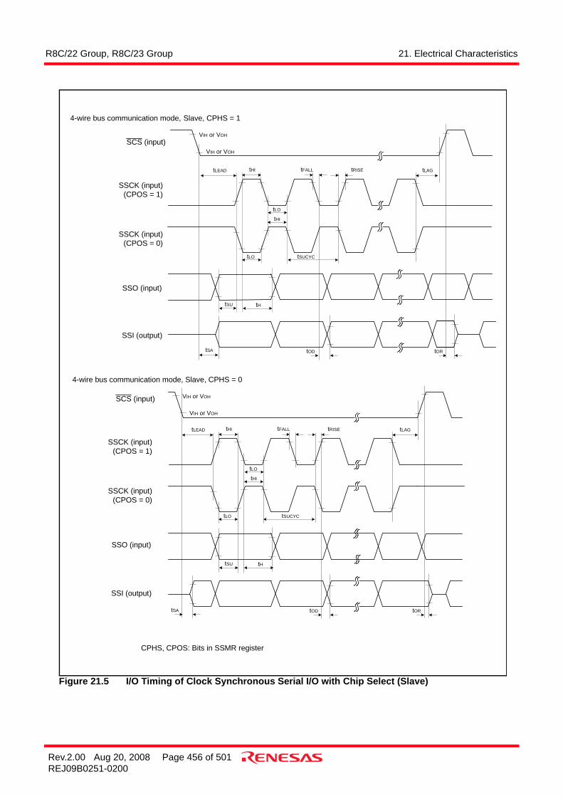
R8C/22 Group, R8C/23 Group 21. Electrical Characteristics
Rev.2.00 Aug 20, 2008 Page 456 of 501REJ09B0251-0200
Figure 21.5 I/O Timing of Clock Synchronous Serial I/O with Chip Select (Slave)
VIH or VOH
VIH or VOH
SCS (input)
SSCK (input)(CPOS = 1)
SSCK (input)(CPOS = 0)
SSO (input)
SSI (output)
4-wire bus communication mode, Slave, CPHS = 1
VIH or VOH
VIH or VOH
tHI
tLO
tHI
tFALL tRISE
tLO tSUCYC
tHtSU
SCS (input)
SSCK (input)(CPOS = 1)
SSCK (input)(CPOS = 0)
SSO (input)
SSI (output)
4-wire bus communication mode, Slave, CPHS = 0
tOD
tLEAD
tSA
tLAG
tOR
tHI
tLO
tHI
tFALL tRISE
tLO tSUCYC
tHtSU
tOD
tLEAD
tSA
tLAG
tOR
CPHS, CPOS: Bits in SSMR register

R8C/22 Group, R8C/23 Group 21. Electrical Characteristics
Rev.2.00 Aug 20, 2008 Page 457 of 501REJ09B0251-0200
Figure 21.6 I/O Timing of Clock Synchronous Serial I/O with Chip Select(Clock Synchronous Communication Mode)
VIH or VOH
tHI
tLO tSUCYC
tOD
tHtSU
SSCK
SSO (output)
SSI (input)
VIH or VOH

R8C/22 Group, R8C/23 Group 21. Electrical Characteristics
Rev.2.00 Aug 20, 2008 Page 458 of 501REJ09B0251-0200
NOTES:1. VCC = 2.7 to 5.5 V, VSS = 0V at Topr = -40 to 85°C (D, J version) / -40 to 125°C (K version), unless otherwise specified.2. 1tCYC = 1/f1(s)
Figure 21.7 I/O Timing of I2C Bus Interface
Table 21.13 Timing Requirements of I2C Bus Interface(1)
Symbol Parameter ConditionsStandard
UnitMin. Typ. Max.
tSCL SCL input cycle time 12tCYC +600(2)
− − ns
tSCLH SCL input “H” width 3tCYC +300(2)
− − ns
tSCLL SCL input “L” width 5tCYC +500(2)
− − ns
tsf SCL, SDA input falling time − − 300 nstSP SCL, SDA input spike pulse rejection time − − 1tCYC(2) nstBUF SDA input bus-free time 5tCYC(2) − − nstSTAH Start condition input hole time 3tCYC(2) − − nstSTAS Retransmit start condition input setup time 3tCYC(2) − − ns
tSTOP Stop condition input setup time 3tCYC(2) − − ns
tSOAS Data input setup time 1tCYC + 20(2)
− − ns
tSDAH Data input hold time 0 − − ns
SDA
SCL
tBUF
VIH
VIL
P(2) S(1)
tSTAH tSCLH
tSCLLtSf tSr
tSCL tSDAH
Sr(3) P(2)
tSDAS
tSTAStSP tSTOP
NOTES:1. Start condition2. Stop condition3. Retransmit “Start” condition

R8C/22 Group, R8C/23 Group 21. Electrical Characteristics
Rev.2.00 Aug 20, 2008 Page 459 of 501REJ09B0251-0200
NOTE:1. VCC = 4.2 to 5.5 V at Topr = -40 to 85°C (D, J version) / -40 to 125°C (K version), f(XIN) = 20 MHz, unless otherwise specified.
Table 21.14 Electrical Characteristics (1) [VCC = 5 V]
Symbol Parameter ConditionStandard
UnitMin. Typ. Max.
VOH Output “H” Voltage Except XOUT IOH = -5 mA VCC − 2.0 − VCC VIOH = -200 µA VCC − 0.3 − VCC V
XOUT Drive capacity HIGH
IOH = -1 mA VCC − 2.0 − VCC V
Drive capacity LOW
IOH = -500 µA VCC − 2.0 − VCC V
VOL Output “L” Voltage Except XOUT IOL = 5 mA − − 2.0 VIOL = 200 µA − − 0.45 V
XOUT Drive capacity HIGH
IOL = 1 mA − − 2.0 V
Drive capacity LOW
IOL = 500 µA − − 2.0 V
VT+-VT- Hysteresis INT0, INT1, INT2, INT3, KI0, KI1, KI2, KI3, TRAIO, RXD0, RXD1, CLK0, SSI, SCL, SDA, SSO
0.1 0.5 − V
RESET 0.1 1.0 − V
IIH Input “H” current VI = 5 V, Vcc = 5 V − − 5.0 µAIIL Input “L” current VI = 0 V, Vcc = 5 V − − -5.0 µARPULLUP Pull-Up Resistance VI = 0 V, Vcc = 5 V 30 50 167 kΩRfXIN Feedback
ResistanceXIN − 1.0 − MΩ
VRAM RAM Hold Voltage During stop mode 2.0 − − V

R8C/22 Group, R8C/23 Group 21. Electrical Characteristics
Rev.2.00 Aug 20, 2008 Page 460 of 501REJ09B0251-0200
Table 21.15 Electrical Characteristics (2) [VCC = 5 V](Topr = -40 to 85°C (D, J version) / -40 to 125°C (K version), Unless Otherwise Specified.)
Symbol Parameter ConditionStandard
UnitMin. Typ. Max.
ICC Power supply current (VCC = 3.3 to 5.5 V)In single-chip mode, the output pins are open and other pins are VSS
High-clock mode
XIN = 20 MHz (square wave)High-speed on-chip oscillator offLow-speed on-chip oscillator on = 125 kHzNo division
− 12.5 25.0 mA
XIN = 16 MHz (square wave)High-speed on-chip oscillator offLow-speed on-chip oscillator on = 125 kHzNo division
− 10.0 20.0 mA
XIN = 10 MHz (square wave)High-speed on-chip oscillator offLow-speed on-chip oscillator on = 125 kHzNo division
− 6.5 − mA
XIN = 20 MHz (square wave)High-speed on-chip oscillator offLow-speed on-chip oscillator on = 125 kHzDivide-by-8
− 6.5 − mA
XIN = 16MHz (square wave)High-speed on-chip oscillator offLow-speed on-chip oscillator on = 125 kHzDivide-by-8
− 5.0 − mA
XIN = 10 MHz (square wave)High-speed on-chip oscillator offLow-speed on-chip oscillator on = 125 kHzDivide-by-8
− 3.5 − mA
High-speed on-chip oscillator mode
XIN clock offHigh-speed on-chip oscillator on fOCO = 10 MHzLow-speed on-chip oscillator on = 125 kHzNo division
− 6.5 13.0 mA
XIN clock offHigh-speed on-chip oscillator on fOCO= 10 MHzLow-speed on-chip oscillator on = 125 kHzDivide-by-8
− 3.2 − mA
Low-speed on-chip oscillator mode
XIN clock offHigh-speed on-chip oscillator offLow-speed on-chip oscillator on = 125 kHzDivide-by-8FMR47 = 1
− 150 300 µA
Wait mode XIN clock offHigh-speed on-chip oscillator offLow-speed on-chip oscillator on = 125 kHzWhile a WAIT instruction is executedPeripheral clock operationVCA20 = 0VCA26 = VCA27 = 0
− 60 120 µA
XIN clock offHigh-speed on-chip oscillator offLow-speed on-chip oscillator on = 125 kHzWhile a WAIT instruction is executedPeripheral clock offVCA20 = 0VCA26 = VCA27 = 0
− 38 76 µA
Stop modeTopr = 25°C
XIN clock offHigh-speed on-chip oscillator offLow-speed on-chip oscillator offCM10 = 1Peripheral clock offVCA26 = VCA27 = 0
− 0.8 3.0 µA
Stop modeTopr = 85°C
XIN clock offHigh-speed on-chip oscillator offLow-speed on-chip oscillator offCM10 = 1Peripheral clock offVCA26 = VCA27 = 0
− 1.2 − µA
Stop modeTopr = 125°C
XIN clock offHigh-speed on-chip oscillator offLow-speed on-chip oscillator offCM10 = 1Peripheral clock offVCA26 = VCA27 = 0
− 4.0 − µA

R8C/22 Group, R8C/23 Group 21. Electrical Characteristics
Rev.2.00 Aug 20, 2008 Page 461 of 501REJ09B0251-0200
Timing Requirements (Unless Otherwise Specified: VCC = 5 V, VSS = 0 V at Topr = 25°C) [VCC = 5 V]
Figure 21.8 XIN Input Timing Diagram when VCC = 5 V
Figure 21.9 TRAIO Input Timing Diagram when VCC = 5 V
Table 21.16 XIN Input
Symbol ParameterStandard
UnitMin. Max.
tc(XIN) XIN input cycle time 50 − nstWH(XIN) XIN input “H” width 25 − nstWL(XIN) XIN input “L” width 25 − ns
Table 21.17 TRAIO Input
Symbol ParameterStandard
UnitMin. Max.
tc(TRAIO) TRAIO input cycle time 100 − nstWH(TRAIO) TRAIO input “H” width 40 − nstWL(TRAIO) TRAIO input “L” width 40 − ns
Vcc = 5V
XIN input
tWH(XIN)
tc(XIN)
tWL(XIN)
Vcc = 5V
TRAIO input
tWH(TRAIO)
tc(TRAIO)
tWL(TRAIO)
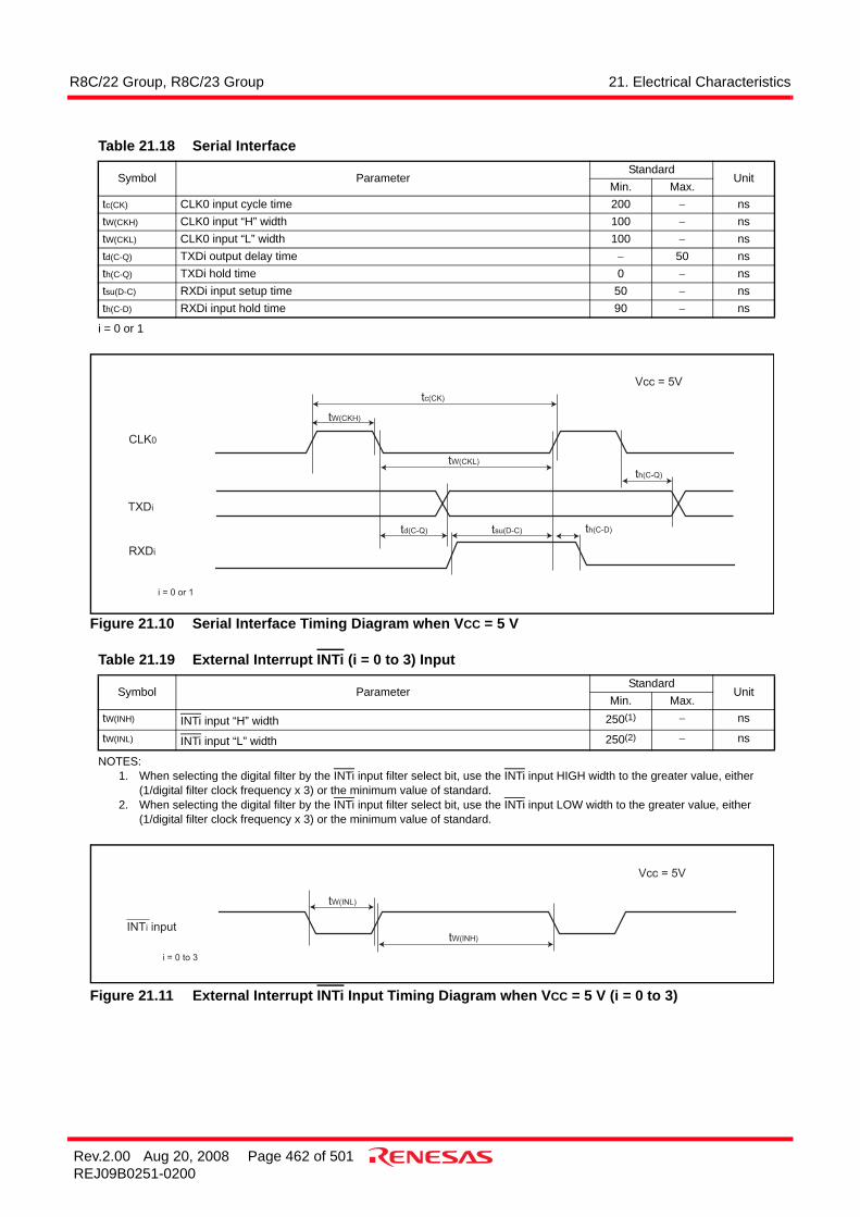
R8C/22 Group, R8C/23 Group 21. Electrical Characteristics
Rev.2.00 Aug 20, 2008 Page 462 of 501REJ09B0251-0200
i = 0 or 1
Figure 21.10 Serial Interface Timing Diagram when VCC = 5 V
NOTES:1. When selecting the digital filter by the INTi input filter select bit, use the INTi input HIGH width to the greater value, either
(1/digital filter clock frequency x 3) or the minimum value of standard.2. When selecting the digital filter by the INTi input filter select bit, use the INTi input LOW width to the greater value, either
(1/digital filter clock frequency x 3) or the minimum value of standard.
Figure 21.11 External Interrupt INTi Input Timing Diagram when VCC = 5 V (i = 0 to 3)
Table 21.18 Serial Interface
Symbol ParameterStandard
UnitMin. Max.
tc(CK) CLK0 input cycle time 200 − nstW(CKH) CLK0 input “H” width 100 − nstW(CKL) CLK0 input “L” width 100 − nstd(C-Q) TXDi output delay time − 50 nsth(C-Q) TXDi hold time 0 − nstsu(D-C) RXDi input setup time 50 − nsth(C-D) RXDi input hold time 90 − ns
Table 21.19 External Interrupt INTi (i = 0 to 3) Input
Symbol ParameterStandard
UnitMin. Max.
tW(INH) INTi input “H” width 250(1) − ns
tW(INL) INTi input “L” width 250(2) − ns
i = 0 or 1
Vcc = 5V
CLK0
TXDi
RXDi
tW(CKH)
tc(CK)
tW(CKL)
th(C-Q)
th(C-D)tsu(D-C)td(C-Q)
i = 0 to 3
Vcc = 5V
INTi input
tW(INL)
tW(INH)

R8C/22 Group, R8C/23 Group 21. Electrical Characteristics
Rev.2.00 Aug 20, 2008 Page 463 of 501REJ09B0251-0200
NOTE:1. VCC = 2.7 to 3.3 V at Topr = -40 to 85°C (D, J version) / -40 to 125°C (K version), f(XIN) = 10 MHz, unless otherwise specified.
Table 21.20 Electrical Characteristics (3) [VCC = 3 V]
Symbol Parameter ConditionStandard
UnitMin. Typ. Max.
VOH Output “H” voltage Except XOUT IOH = -1 mA VCC − 0.5 − VCC VXOUT Drive capacity
HIGHIOH = -0.1 mA VCC − 0.5 − VCC V
Drive capacity LOW
IOH = -50 µA VCC − 0.5 − VCC V
VOL Output “L” voltage Except XOUT IOL = 1 mA − − 0.5 VXOUT Drive capacity
HIGHIOL = 0.1 mA − − 0.5 V
Drive capacity LOW
IOL = 50 µA − − 0.5 V
VT+-VT- Hysteresis INT0, INT1, INT2, INT3, KI0, KI1, KI2, KI3, TRAIO, RXD0, RXD1, CLK0, SSI, SCL, SDA, SSO
0.1 0.3 − V
RESET 0.1 0.4 − V
IIH Input “H” current VI = 3 V, Vcc = 3 V − − 4.0 µAIIL Input “L” current VI = 0 V, Vcc = 3 V − − -4.0 µARPULLUP Pull-up resistance VI = 0 V, Vcc = 3 V 66 160 500 kΩRfXIN Feedback resistance XIN − 3.0 − MΩVRAM RAM hold voltage During stop mode 2.0 − − V

R8C/22 Group, R8C/23 Group 21. Electrical Characteristics
Rev.2.00 Aug 20, 2008 Page 464 of 501REJ09B0251-0200
Table 21.21 Electrical Characteristics (4) [VCC = 3 V](Topr = -40 to 85°C (D, J version) / -40 to 125°C (K version), Unless Otherwise Specified.)
Symbol Parameter ConditionStandard
UnitMin. Typ. Max.
ICC Power supply current (VCC = 2.7 to 3.3 V)In single-chip mode, the output pins are open and other pins are VSS
High-clock mode
XIN = 20 MHz (square wave)High-speed on-chip oscillator offLow-speed on-chip oscillator on = 125 kHzNo division
− 11.5 23.0 mA
XIN = 16 MHz (square wave)High-speed on-chip oscillator offLow-speed on-chip oscillator on = 125 kHzNo division
− 9.5 19.0 mA
XIN = 10 MHz (square wave)High-speed on-chip oscillator offLow-speed on-chip oscillator on = 125 kHzNo division
− 6.0 12.0 mA
XIN = 20 MHz (square wave)High-speed on-chip oscillator offLow-speed on-chip oscillator on = 125 kHzDivide-by-8
− 5.5 − mA
XIN = 16 MHz (square wave)High-speed on-chip oscillator offLow-speed on-chip oscillator on = 125 kHzDivide-by-8
− 4.5 − mA
XIN = 10 MHz (square wave)High-speed on-chip oscillator offLow-speed on-chip oscillator on = 125 kHzDivide-by-8
− 3.0 − mA
High-speed on-chip oscillator mode
XIN clock offHigh-speed on-chip oscillator on fOCO = 10 MHzLow-speed on-chip oscillator on = 125 kHzNo division
− 6.3 12.6 mA
XIN clock offHigh-speed on-chip oscillator on fOCO = 10 MHzLow-speed on-chip oscillator on = 125 kHzDivide-by-8
− 3.1 − mA
Low-speed on-chip oscillator mode
XIN clock offHigh-speed on-chip oscillator offLow-speed on-chip oscillator on = 125 kHzDivide-by-8FMR47 = 1
− 145 290 µA
Wait mode XIN clock offHigh-speed on-chip oscillator offLow-speed on-chip oscillator on = 125 kHzWhile a WAIT instruction is executedPeripheral clock operationVCA20 = 0VCA26 = VCA27 = 0
− 56 112 µA
XIN clock offHigh-speed on-chip oscillator offLow-speed on-chip oscillator on = 125 kHzWhile a WAIT instruction is executedPeripheral clock offVCA20 = 0VCA26 = VCA27 = 0
− 35 70 µA
Stop modeTopr = 25°C
XIN clock offHigh-speed on-chip oscillator offLow-speed on-chip oscillator offCM10 = 1Peripheral clock offVCA26 = VCA27 = 0
− 0.7 3.0 µA
Stop modeTopr = 85°C
XIN clock offHigh-speed on-chip oscillator offLow-speed on-chip oscillator offCM10 = 1Peripheral clock offVCA26 = VCA27 = 0
− 1.1 − µA
Stop modeTopr = 125°C
XIN clock offHigh-speed on-chip oscillator offLow-speed on-chip oscillator offCM10 = 1Peripheral clock offVCA26 = VCA27 = 0
− 3.8 − µA
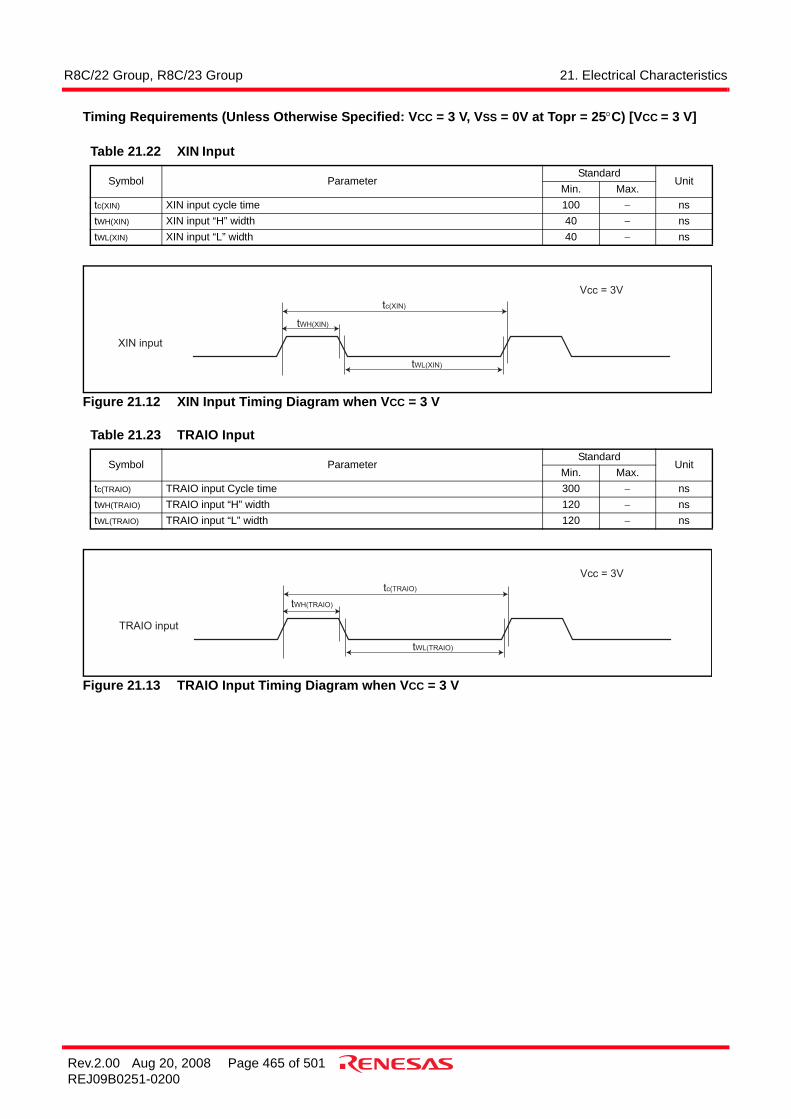
R8C/22 Group, R8C/23 Group 21. Electrical Characteristics
Rev.2.00 Aug 20, 2008 Page 465 of 501REJ09B0251-0200
Timing Requirements (Unless Otherwise Specified: VCC = 3 V, VSS = 0V at Topr = 25°C) [VCC = 3 V]
Figure 21.12 XIN Input Timing Diagram when VCC = 3 V
Figure 21.13 TRAIO Input Timing Diagram when VCC = 3 V
Table 21.22 XIN Input
Symbol ParameterStandard
UnitMin. Max.
tc(XIN) XIN input cycle time 100 − nstWH(XIN) XIN input “H” width 40 − nstWL(XIN) XIN input “L” width 40 − ns
Table 21.23 TRAIO Input
Symbol ParameterStandard
UnitMin. Max.
tc(TRAIO) TRAIO input Cycle time 300 − nstWH(TRAIO) TRAIO input “H” width 120 − nstWL(TRAIO) TRAIO input “L” width 120 − ns
Vcc = 3V
XIN input
tWH(XIN)
tc(XIN)
tWL(XIN)
Vcc = 3V
TRAIO input
tWH(TRAIO)
tc(TRAIO)
tWL(TRAIO)

R8C/22 Group, R8C/23 Group 21. Electrical Characteristics
Rev.2.00 Aug 20, 2008 Page 466 of 501REJ09B0251-0200
i = 0 or 1
Figure 21.14 Serial Interface Timing Diagram when VCC = 3 V
NOTES:1. When selecting the digital filter by the INTi input filter select bit, use the INTi input HIGH width to the greater value, either
(1/digital filter clock frequency x 3) or the minimum value of standard.2. When selecting the digital filter by the INTi input filter select bit, use the INTi input LOW width to the greater value, either
(1/digital filter clock frequency x 3) or the minimum value of standard.
Figure 21.15 External Interrupt INTi Input Timing Diagram when VCC = 3 V (i = 0 to 3)
Table 21.24 Serial Interface
Symbol ParameterStandard
UnitMin. Max.
tc(CK) CLK0 input cycle time 300 − nstW(CKH) CLK0 input “H” width 150 − nstW(CKL) CLK0 input “L” width 150 − nstd(C-Q) TXDi output delay time − 80 nsth(C-Q) TXDi hold time 0 − nstsu(D-C) RXDi input setup time 70 − nsth(C-D) RXDi input hold time 90 − ns
Table 21.25 External Interrupt INTi (i = 0 to 3) Input
Symbol ParameterStandard
UnitMin. Max.
tW(INH) INTi input “H” width 380(1) − ns
tW(INL) INTi input “L” width 380(2) − ns
i = 0 or 1
Vcc = 3V
CLK0
TXDi
RXDi
tW(CKH)
tc(CK)
tW(CKL)
th(C-Q)
th(C-D)tsu(D-C)td(C-Q)
i = 0 to 3
Vcc = 3V
INTi input
tW(INL)
tW(INH)

R8C/22 Group, R8C/23 Group 22. Usage Notes
Rev.2.00 Aug 20, 2008 Page 467 of 501REJ09B0251-0200
22. Usage Notes
22.1 Notes on Clock Generation Circuit
22.1.1 Stop ModeWhen entering stop mode, set the FMR01 bit to “0” (CPU rewrite mode disabled) and the CM10 bit to “1” (stopmode). An instruction queue pre-reads 4 bytes from the instruction which sets the CM10 bit in the CM1 registerto “1” (stop mode) and the program stops. Insert at least 4 NOP instructions following the JMP.B instructionafter the instruction which sets the CM10 bit to “1”.
• Example to enter stop modeBCLR 1,FMR0 ; CPU rewrite mode disabledBSET 0,PRCR ; Protect disabledFSET I ; Enable interruptBSET 0,CM1 ; Stop modeJMP.B LABEL_001
LABEL_001:NOPNOPNOPNOP
22.1.2 Wait ModeWhen entering wait mode, set the FMR01 bit to “0” (CPU rewrite mode disabled) and execute the WAITinstruction. An instruction queue pre-reads 4 bytes from the WAIT instruction and the program stops. Insert atleast 4 NOP instructions after the WAIT instruction.
• Example to execute the WAIT instructionBCLR 1,FMR0 ; CPU rewrite mode disabledFSET I ; Enable interruptWAIT ; Wait modeNOPNOPNOPNOP
22.1.3 Oscillation Stop Detection FunctionSince the oscillation stop detection function cannot be used if the XIN clock frequency is less than 2 MHz, setthe OCD1 to OCD0 bits to 00b.
22.1.4 Oscillation Circuit ConstantsAsk the maker of the oscillator to specify the beat oscillation circuit constants on your system.

R8C/22 Group, R8C/23 Group 22. Usage Notes
Rev.2.00 Aug 20, 2008 Page 468 of 501REJ09B0251-0200
22.2 Notes on Interrupts
22.2.1 Reading Address 00000hDo not read the address 00000h by a program. When a maskable interrupt request is acknowledged, the CPUreads interrupt information (interrupt number and interrupt request level) from 00000h in the interruptsequence. At this time, the acknowledged interrupt IR bit is set to 0.If the address 00000h is read in a program, the IR bit for the interrupt which has the highest priority among theenabled interrupts is set to 0. This may cause a problem that the interrupt is canceled, or an unexpected interruptis generated.
22.2.2 SP SettingSet any value in the SP before an interrupt is acknowledged. The SP is set to 0000h after reset. Therefore, if aninterrupt is acknowledged before setting any value in the SP, the program may run out of control.
22.2.3 External Interrupt and Key Input InterruptEither an “L” level or an “H” level of width shown in the Electrical Characteristics is necessary for the signalinput to the INT0 to INT3 pins and KI0 to KI3 pins regardless of the CPU clocks. For details, refer to Table21.19 External Interrupt INTi (i = 0 to 3) Input, Table 21.25 External Interrupt INTi (i = 0 to 3) Input.
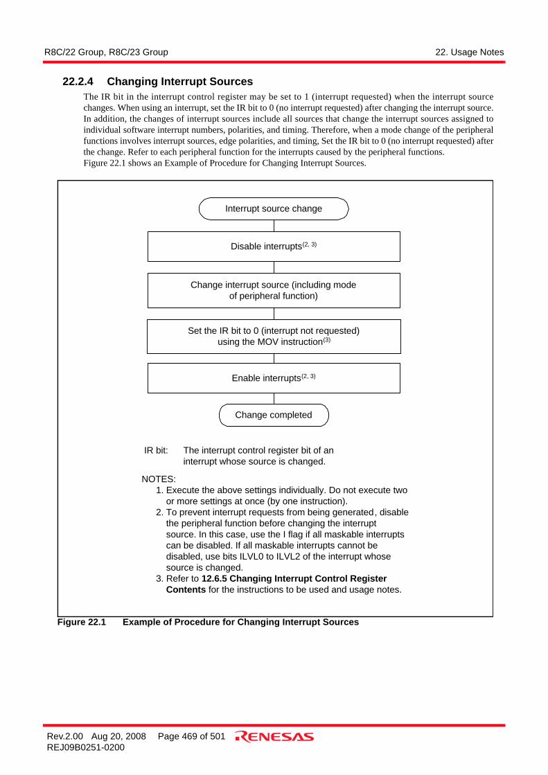
R8C/22 Group, R8C/23 Group 22. Usage Notes
Rev.2.00 Aug 20, 2008 Page 469 of 501REJ09B0251-0200
22.2.4 Changing Interrupt SourcesThe IR bit in the interrupt control register may be set to 1 (interrupt requested) when the interrupt sourcechanges. When using an interrupt, set the IR bit to 0 (no interrupt requested) after changing the interrupt source.In addition, the changes of interrupt sources include all sources that change the interrupt sources assigned toindividual software interrupt numbers, polarities, and timing. Therefore, when a mode change of the peripheralfunctions involves interrupt sources, edge polarities, and timing, Set the IR bit to 0 (no interrupt requested) afterthe change. Refer to each peripheral function for the interrupts caused by the peripheral functions. Figure 22.1 shows an Example of Procedure for Changing Interrupt Sources.
Figure 22.1 Example of Procedure for Changing Interrupt Sources
NOTES:1. Execute the above settings individually. Do not execute two
or more settings at once (by one instruction).2. To prevent interrupt requests from being generated, disable
the peripheral function before changing the interruptsource. In this case, use the I flag if all maskable interruptscan be disabled. If all maskable interrupts cannot bedisabled, use bits ILVL0 to ILVL2 of the interrupt whosesource is changed.
3. Refer to 12.6.5 Changing Interrupt Control RegisterContents for the instructions to be used and usage notes.
Interrupt source change
Disable interrupts(2, 3)
Set the IR bit to 0 (interrupt not requested)using the MOV instruction(3)
Change interrupt source (including modeof peripheral function)
Enable interrupts(2, 3)
Change completed
IR bit: The interrupt control register bit of aninterrupt whose source is changed.

R8C/22 Group, R8C/23 Group 22. Usage Notes
Rev.2.00 Aug 20, 2008 Page 470 of 501REJ09B0251-0200
22.2.5 Changing Interrupt Control Register Contents(a) Each interrupt control register can only be changed while interrupt requests corresponding to that
register are not generated. If interrupt requests may be generated, disable the interrupts before changingthe interrupt control register.
(b) When changing any interrupt control register after disabling interrupts, be careful with the instructionsto be used.When changing any bit other than IR bitIf an interrupt request corresponding to that register is generated while executing the instruction, the IRbit may not be set to 1 (interrupt requested), and the interrupt request may be ignored. If this causes aproblem, use the following instructions to change the register.Instructions to use: AND, OR, BCLR, BSETWhen changing IR bitIf the IR bit is set to 0 (interrupt not requested), it may not be set to 0 depending on the instruction to beused. Therefore, use the MOV instruction to set the IR bit to 0.
(c) When disabling interrupts using the I flag, set the I flag according to the following sample programs.Refer to (b) for the change of interrupt control registers in the sample programs.
Sample programs 1 to 3 are preventing the I flag from being set to 1 (interrupt enables) before changing theinterrupt control register for reasons of the internal bus or the instruction queue buffer.
Example 1: Use NOP instructions to prevent I flag being set to 1 before interrupt control register ischanged
INT_SWITCH1:FCLR I ; Disable interruptsAND.B #00H,0056H ; Set TRAIC register to 00hNOP ;NOPFSET I ; Enable interrupts
Example 2: Use dummy read to have FSET instruction waitINT_SWITCH2:
FCLR I ; Disable interruptsAND.B #00H,0056H ; Set TRAIC register to 00hMOV.W MEM,R0 ; Dummy readFSET I ; Enable interrupts
Example 3: Use POPC instruction to change I flagINT_SWITCH3:
PUSHC FLGFCLR I ; Disable interruptsAND.B #00H,0056H ; Set TRAIC register to 00hPOPC FLG ; Enable interrupts

R8C/22 Group, R8C/23 Group 22. Usage Notes
Rev.2.00 Aug 20, 2008 Page 471 of 501REJ09B0251-0200
22.3 Notes on Timers
22.3.1 Notes on Timer RA• Timer RA stops counting after reset. Set the value to timer RA and timer RA prescaler before the count
starts.• Even if the prescaler and timer RA is read out in 16-bit units, these registers are read by 1 byte in the MCU.
Consequently, the timer value may be updated during the period these two registers are being read.• In pulse width measurement mode and pulse period measurement mode, the TEDGF and TUNDF bits in
the TRACR register can be set to 0 by writing 0 to these bits by a program. However, these bits remainunchanged when 1 is written. When using the READ-MODIFY-WRITE instruction for the TRACRregister, the TEDGF or TUNDF bit may be set to 0 although these bits are set to 1 while the instruction isexecuted. At the time, write 1 to the TEDGF or TUNDF bit which is not supposed to be set to 0 with theMOV instruction.
• When changing to pulse width measurement mode and pulse period measurement mode from other mode,the contents of the TEDGF and TUNDF bits are indeterminate. Write 0 to the TEDGF and TUNDF bitsbefore the count starts.
• The TEDGF bit may be set to 1 by timer RA prescaler underflow which is generated for the first time sincethe count starts.
• When using the pulse period measurement mode, leave two periods or more of timer RA prescalerimmediately after count starts, and set the TEDGF bit to 0.
• The TCSTF bit retains 0 (count stops) for 0 to 1 cycle of the count source after setting the TSTART bit to 1(count starts) while the count stops.During this time, do not access registers associated with timer RA(1) other than the TCSTF bit. Timer RAstarts counting at the first valid edge of the count source after The TCSTF bit is set to 1 (during count).The TCSTF bit retains 1 for 0 to 1 cycle of the count source after setting the TSTART bit to 0 (count stops)while the count is performing. Timer RA counting is stopped when the TCSTF bit is set to 0.During this time, do not access registers associated with timer RA(1) other than the TCSTF bit.
NOTE:1. Registers associated with timer RA: TRACR, TRAIOC, TRAMR, TRAPRE, TRA
• When the TRAPRE register is continuously written during count operation (TCSTF bit is set to 1), allowthree or more cycles of the count source clock for each write interval.
• When the TRA register is continuously written during count operation (TCSTF bit is set to 1), allow threeor more cycles of the prescaler underflow for each write interval.

R8C/22 Group, R8C/23 Group 22. Usage Notes
Rev.2.00 Aug 20, 2008 Page 472 of 501REJ09B0251-0200
22.3.2 Notes on Timer RB• Timer RB stops counting after reset. Set the value to timer RB and timer RB prescaler before the count
starts.• Even if the prescaler and timer RB is read out in 16-bit units, these registers are read by 1 byte in the MCU.
Consequently, the timer value may be updated during the period these two registers are being read.• In programmable one-shot generation mode and programmable wait one-shot generation mode, when
setting the TSTART bit in the TRBCR register to 0, 0 (stops counting) or setting the TOSSP bit in theTRBOCR register to 1 (stops one-shot), the timer reloads the value of reload register and stops. Therefore,read the timer count value in programmable one-shot generation mode and programmable wait one-shotgeneration mode before the timer stops.
• The TCSTF bit retains 0 (count stops) for 1 to 2 cycles of the count source after setting the TSTART bit to1 (count starts) while the count stops.During this time, do not access registers associated with timer RB(1) other than the TCSTF bit.The TCSTF bit retains 1 for 1 to 2 cycles of the count source after setting the TSTART bit to 0 (countstops) while the count is performing. Timer RB counting is stopped when the TCSTF bit is set to 0.During this time, do not access registers associated with timer RB(1) other than the TCSTF bit.
NOTE:1. Registers associated with timer RB: TRBCR, TRBOCR, TRBIOC, TRBMR, TRBPRE, TRBSC, TRBPR
• If the TSTOP bit in the TRBCR register is set to 1 during timer operation, timer RB stops immediately.• If 1 is written to the TOSST or TOSSP bit in the TRBOCR register, the value of the TOSSTF bit changes
after one or two cycles of the count source have elapsed. If the TOSSP bit is written to 1 during the periodbetween when the TOSST bit is written to 1 and when the TOSSTF bit is set to 1, the TOSSTF bit may beset to either 0 or 1 depending on the content state. Likewise, if the TOSST bit is written to 1 during theperiod between when the TOSSP bit is written to 1 and when the TOSSTF bit is set to 0, the TOSSTF bitmay be set to either 0 or 1.
22.3.2.1 Timer modeThe following workaround should be performed in timer mode. To write to registers TRBPRE and TRBPR during count operation (TCSTF bit is set to 1), note the followingpoints:
• When the TRBPRE register is written continuously, allow three or more cycles of the count source for eachwrite interval.
• When the TRBPR register is written continuously, allow three or more cycles of the prescaler underflowfor each write interval.

R8C/22 Group, R8C/23 Group 22. Usage Notes
Rev.2.00 Aug 20, 2008 Page 473 of 501REJ09B0251-0200
22.3.2.2 Programmable waveform generation modeThe following three workarounds should be performed in programmable waveform generation mode.
(1) To write to registers TRBPRE and TRBPR during count operation (TCSTF bit is set to 1), note thefollowing points:
• When the TRBPRE register is written continuously, allow three or more cycles of the count source for eachwrite interval.
• When the TRBPR register is written continuously, allow three or more cycles of the prescaler underflowfor each write interval.
(2) To change registers TRBPRE and TRBPR during count operation (TCSTF bit is set to 1), synchronizethe TRBO output cycle using a timer RB interrupt, etc. This operation should be preformed only once inthe same output cycle. Also, make sure that writing to the TRBPR register does not occur during periodA shown in Figures 22.2 and 22.3.
The following shows the detailed workaround examples.• Workaround example (a):
As shown in Figure 22.2, write to registers TRBSC and TRBPR in the timer RB interrupt routine. Thesewrite operations must be completed by the beginning of period A.
Figure 22.2 Workaround Example (a) When Timer RB Interrupt is Used
TRBO pin output
Count source/prescaler
underflow signal
Primary period
Period A
IR bit inTRBIC register
Secondary period
(b)
Interruptsequence
Instruction ininterrupt routine
Interrupt request isacknowledged
(a)
Interrupt requestis generated
Ensure sufficient time
Set the secondary and thenthe primary register immediately
(a) Period between interrupt request generation and the completion of execution of an instruction. The length of timevaries depending on the instruction being executed.The DIVX instruction requires the longest time, 30 cycles (assuming no wait states and that a register is set asthe divisor).
(b) 20 cycles. 21 cycles for address match and single-step interrupts.

R8C/22 Group, R8C/23 Group 22. Usage Notes
Rev.2.00 Aug 20, 2008 Page 474 of 501REJ09B0251-0200
• Workaround example (b): As shown in Figure 22.3 detect the start of the primary period by the TRBO pin output level and write toregisters TRBSC and TRBPR. These write operations must be completed by the beginning of period A.If the port register’s bit value is read after the port direction register’s bit corresponding to the TRBO pin isset to 0 (input mode), the read value indicates the TRBO pin output value.
Figure 22.3 Workaround Example (b) When TRBO Pin Output Value is Read
(3) To stop the timer counting in the primary period, use the TSTOP bit in the TRBCR register. In this case,registers TRBPRE and TRBPR are initialized and their values are set to the values after reset.
22.3.2.3 Programmable one-shot generation modeThe following two workarounds should be performed in programmable one-shot generation mode.
(1) To write to registers TRBPRE and TRBPR during count operation (TCSTF bit is set to 1), note thefollowing points:
• When the TRBPRE register is written continuously during count operation (TCSTF bit is set to 1), allowthree or more cycles of the count source for each write interval.
• When the TRBPR register is written continuously during count operation (TCSTF bit is set to 1), allowthree or more cycles of the prescaler underflow for each write interval.
(2) Do not set both the TRBPRE and TRBPR registers to 00h.
TRBO pin output
Count source/prescaler
underflow signal
Primary period
Period A
Read value of the port register’sbit corresponding to the TRBO pin
(when the bit in the port directionregister is set to 0)
Secondary period
(i)
The TRBO output inversionis detected at the end of the
secondary period.
Ensure sufficient time
Upon detecting (i), set the secondary andthen the primary register immediately.
(ii) (iii)

R8C/22 Group, R8C/23 Group 22. Usage Notes
Rev.2.00 Aug 20, 2008 Page 475 of 501REJ09B0251-0200
22.3.2.4 Programmable wait one-shot generation modeThe following three workarounds should be performed in programmable wait one-shot generation mode.
(1) To write to registers TRBPRE and TRBPR during count operation (TCSTF bit is set to 1), note thefollowing points:
• When the TRBPRE register is written continuously, allow three or more cycles of the count source for eachwrite interval.
• When the TRBPR register is written continuously, allow three or more cycles of the prescaler underflowfor each write interval.
(2) Do not set both the TRBPRE and TRBPR registers to 00h.
(3) Set registers TRBSC and TRBPR using the following procedure.(a) To use “INT0 pin one-shot trigger enabled” as the count start condition
Set the TRBSC register and then the TRBPR register. At this time, after writing to the TRBPRregister, allow an interval of 0.5 or more cycles of the count source before trigger input from theINT0 pin.
(b) To use “writing 1 to TOSST bit” as the start conditionSet the TRBSC register, the TRBPR register, and then TOSST bit. At this time, after writing to theTRBPR register, allow an interval of 0.5 or more cycles of the count source before writing to theTOSST bit.

R8C/22 Group, R8C/23 Group 22. Usage Notes
Rev.2.00 Aug 20, 2008 Page 476 of 501REJ09B0251-0200
22.3.3 Notes on Timer RD
22.3.3.1 TRDSTR Register• Set the TRDSTR register using the MOV instruction.• When the CSELi (i = 0 or 1) is set to 0 (the count stops at compare match of registers TRDi and
TRDGRAi), the count does not stop and the TSTARTi bit remains unchanged even if 0 (count stops) iswritten to the TSTARTi bit.Therefore, set the TSTARTi bit to 0 to change other bits without changing the TSTARTi bit when theCSELi bit is set to 0.To stop counting by a program, set the TSTARTi bit to 0 after setting the CSELi bit to 1. Although theCSELi bit is set to 1 and the TSTARTi bit is set to 0 at the same time (with 1 instruction), the count cannotbe stopped.
• Table 22.1 lists the TRDIOji (j = A, B, C, or D) Pin Output Level when Count Stops to use the TRDIOji pinwith the timer RD output.
22.3.3.2 TRDi Register (i = 0 or 1)• When writing the value to the TRDi register by a program while the TSTARTi bit in the TRDSTR register
is set to 1 (count starts), avoid to overlap with the timing to set the TRDi register to 0000h, and then write.When the timing to set the TRDi register to 0000h overlaps with the timing to write the value to the TRDiregister, the value is not written and the TRDi register is set to 0000h.
These precautions are applicable when selecting the following by the CCLR2 to CCLR0 bits in the TRDCRi register.- 001b (clear by the TRDi register at the compare match with the TRDGRAi register)- 010b (clear by the TRDi register at the compare match with the TRDGRBi register.)- 011b (synchronous clear)- 101b (clear by the TRDi register at the compare match with the TRDGRCi register.)- 110b (clear by the TRDi register at the compare match with the TRDGRDi register.)
• When writing the value to the TRDi register and continuously reading the same register, the value beforewriting may be read. In this case, execute the JMP.B instruction between the writing and reading.
Program Example MOV.W #XXXXh, TRD0 ;WritingJMP.B L1 ;JMP.B
L1: MOV.W TRD0,DATA ;Reading
22.3.3.3 TRDSRi Register (i = 0 or 1)When writing the value to the TRDSRi register and continuously reading the same register, the value beforewriting may be read. In this case, execute the JMP.B instruction between the writing and reading.
Program Example MOV.B #XXh, TRDSR0 ;WritingJMP.B L1 ;JMP.B
L1: MOV.B TRDSR0,DATA ;Reading
Table 22.1 TRDIOji (j = A, B, C, or D) Pin Output Level when Count StopsCount Stop TRDIOji Pin Output when Count Stops
When the CSELi bit is set to 1, set the TSTARTi bit to 0 and the count stops.
Hold the output level immediately before the count stops.
When the CSELi bit is set to 0, the count stops at compare match of registers TRDi and TRDGRAi.
Hold the output level after output changes by compare match.

R8C/22 Group, R8C/23 Group 22. Usage Notes
Rev.2.00 Aug 20, 2008 Page 477 of 501REJ09B0251-0200
22.3.3.4 Count Source Switch• When switching the count source, switch it after the count stops.
Change procedure(1) Set the TSTARTi (i = 0 or 1) bit in the TRDSTR register to 0 (count stops).(2) Change the TCK2 to TCK0 bits in the TRDCRi register.
• When changing the count source from fOCO40M to the other and stopping fOCO40M, wait 2 cycles ormore of f1 after setting the clock switch, and then stop fOCO40M.
Change procedure(1) Set the TSTARTi (i = 0 or 1) bit in the TRDSTR register to 0 (count stops).(2) Change the TCK2 to TCK0 bits in the TRDCRi register.(3) Wait 2 cycles or more of f1.(4) Set the FRA00 bit in the FRA0 register to 0 (high-speed on-chip oscillator stops).
22.3.3.5 Input Capture Function• Set the pulse width of input capture signal to 3 cycles or more of the Timer RD operation clock. (Refer to
Table 14.11 Timer RD Operation Clocks.)• The value in the TRDi register is transferred to the TRDGRji register after 2 to 3 cycles of the Timer RD
operation clock since the input capture signal is applied to the TRDIOji pin (i = 0 or 1, j = either A, B, C orD) (no digital filter).
22.3.3.6 Reset Synchronous PWM Mode • When reset synchronous PWM mode is used for motor control, use it with OLS0 = OLS1.• Set to reset synchronous PWM mode in the following procedure:
Change procedure(1) Set the TSTART0 bit in the TRDSTR register to 0 (count stops).(2) Set the CMD1 to CMD0 bits in the TRDFCR register to 00b (timer mode, PWM mode, and PWM3
mode).(3) Set the CMD1 to CMD0 bits to 01b (reset synchronous PWM mode).(4) Set the registers associated with other Timer RD again.
22.3.3.7 Complementary PWM Mode• When complementary PWM mode is used for motor control, use it with OLS0 = OLS1.• Change the CMD1 to CMD0 bits in the TRDFCR register in the following procedure.
Change procedure: When setting to complementary PWM mode (including re-set), or changing the transfer timing from the buffer register to the general register in complementary PWM mode.
(1) Set both the TSTART0 and TSTART1 bits in the TRDSTR register to 0 (count stops).(2) Set the CMD1 to CMD0 bits in the TRDFCR register to 00b (timer mode, PWM mode, and PWM3
mode)(3) Set the DMD1 to CMD0 bits to 10b or 11b (complementary PWM mode).(4) Set the registers associated with other Timer RD again.
Change procedure: When stopping complementary PWM mode(1) Set both the TSTART0 and CSEL1 bits in the TRDSTR register to 0 (count stops).(2) Set the CMD1 to CMD bits to 00b (other than reset synchronous PWM mode, complementary PWM
mode)
• Do not write to the TRDGRA0, TRDGRB0, TRDGRA1 and TRDGRB1 registers during operation.When changing the PWM waveform, transfer the value written to the TRDGRD0, TRDGRC1 andTRDGRD1 registers to the TRDGRB0, TRDGRA1 and TRDGRB1 registers using the buffer operation.However, to write data to the TRDGRD0, TRDGRC1, or TRDGRD1 register, set bits BFD0, BFC1, andBFD1 to 0 (general register). After this, bits BFD0, BFC1, and BFD1 may be set to 1 (buffer register).The PWM period cannot be changed.

R8C/22 Group, R8C/23 Group 22. Usage Notes
Rev.2.00 Aug 20, 2008 Page 478 of 501REJ09B0251-0200
• When the value in the TRDGRA0 register is assumed as m, the TRD0 register counts order of m - 1, m, m+ 1, m, m - 1 when changing from increment to decrement. When changing from m to m + 1, the IMFA bit is set to 1. Also, the CMD1 to CMD0 bits in the TRDFCRregister are set to 11b (complementary PWM mode, buffer data transferred by the compare match in theTRD0 and TRDGRA0 registers), the content in the buffer register (TRDGRD0, TRDGRC1, TRDGRD1) istransferred to the general register (TRDGRB0, TRDGRA1, TRDGRB1). For the order of m + 1, m, m - 1 operation, the IMFA bit remains unchanged and data are not transferred tothe register such as the TRDGRA0 register.
Figure 22.4 Operation at Compare Match between Registers TRD0 and TRDGRA0 in Complementary PWM Mode
No changeIMFA bit in
TRDSR0 register
Transferred frombuffer register
TRDGRB0 registerTRDGRA1 registerTRDGRB1 register
Count value in TRD0register
Setting value inTRDGRA0
register m
m + 1
Set to 0 by a program
Not transferred from buffer register
When the CMD1 to CMD0 bits in theTRDFCR register are set to 11b.(Transfer from the buffer register to thegeneral register at the compare matchof the TRD0 register and TRDGRA0register)
1
0
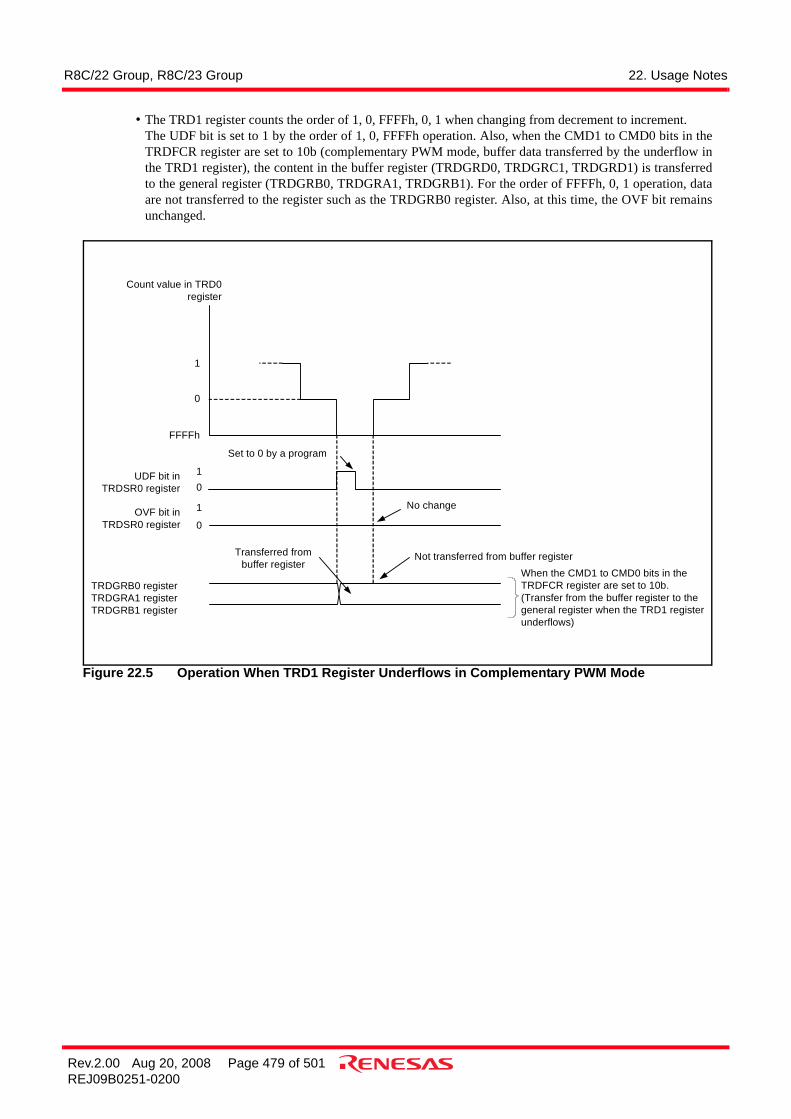
R8C/22 Group, R8C/23 Group 22. Usage Notes
Rev.2.00 Aug 20, 2008 Page 479 of 501REJ09B0251-0200
• The TRD1 register counts the order of 1, 0, FFFFh, 0, 1 when changing from decrement to increment.The UDF bit is set to 1 by the order of 1, 0, FFFFh operation. Also, when the CMD1 to CMD0 bits in theTRDFCR register are set to 10b (complementary PWM mode, buffer data transferred by the underflow inthe TRD1 register), the content in the buffer register (TRDGRD0, TRDGRC1, TRDGRD1) is transferredto the general register (TRDGRB0, TRDGRA1, TRDGRB1). For the order of FFFFh, 0, 1 operation, dataare not transferred to the register such as the TRDGRB0 register. Also, at this time, the OVF bit remainsunchanged.
Figure 22.5 Operation When TRD1 Register Underflows in Complementary PWM Mode
No change
UDF bit inTRDSR0 register
Transferred frombuffer register
TRDGRB0 registerTRDGRA1 registerTRDGRB1 register
Count value in TRD0register
Set to 0 by a program
Not transferred from buffer registerWhen the CMD1 to CMD0 bits in theTRDFCR register are set to 10b.(Transfer from the buffer register to thegeneral register when the TRD1 registerunderflows)
OVF bit inTRDSR0 register
FFFFh
10
1
0
0
1

R8C/22 Group, R8C/23 Group 22. Usage Notes
Rev.2.00 Aug 20, 2008 Page 480 of 501REJ09B0251-0200
• Select with the CMD1 to CMD0 bits for the data transfer timing from the buffer register to the generalregister. However, transfer with the following timing in spite of the value of the CMD1 to CMD0 bits forthe following cases:
Value in buffer register ≥ Value in TRDGRA0 register:Transfer at the underflow in the TRD1 register.And then, when setting the buffer register to 0001h or above and the smaller value than the one in theTRDGRA0 register, and the TRD1 register underflows in the fist time after setting, the value is transferredto the general register. After that, transfer the value with the timing selected by the CMD1 to CMD0 bits.
Figure 22.6 Operation When Value in Buffer Register ≥ Value in TRDGRA0 Register in Complementary PWM Mode
0000h
TRDGRD0 register
TRDIOB0 output
n3n2
m + 1
n3
n2
n1
n2 n1
n3n2 n2 n1n1TRDGRB0 register
Transfer
Transfer byunderflow in TRD1register because ofn3 > m
Transfer byunderflow in TRD1register becauseof first setting ton2 < m
TRDIOD0 output
m: Setting Value in TRDGRA0 Register
The above applies to the following conditions:• The CMD1 to CMD0 bits in the TRDFCR register are set to 11b. (Data in the buffer register is transferred at the compare match in the TRD0 and TRDGRA0 registers in complementary
PWM mode.)• Both the OSL0 and OLS1 bits in the TRDFCR are set to 1. (active ‘H” for normal-phase and counter-phase)
Count value in TRD0register
Count value in TRD1register
Transfer with timing set byCMD1 to CMD0 bits
Transfer with timing set byCMD1 to CMD0 bits
Transfer Transfer Transfer

R8C/22 Group, R8C/23 Group 22. Usage Notes
Rev.2.00 Aug 20, 2008 Page 481 of 501REJ09B0251-0200
When the value in the buffer register is set to 0000h:Transfer by the compare match in the TRD0 and TRDGRA0 registers.And then, when setting the buffer register to 0001h or above and the smaller value than the one in theTRDGRA0 register, and the compare match in the TRD0 and TRDGRA0 registers in the fist time aftersetting, the value is transferred to the general register. After that, transfer the value with the timing selectedby the CMD1 to CMD0 bits.
Figure 22.7 Operation When Value in Buffer Register Is Set to 0000h in Complementary PWM Mode
22.3.3.8 Count Source fOCO40MThe count source fOCO40M can be used with supply voltage VCC = 3.0 to 5.5 V. For supply voltage other thanthat, do not set bits TCK2 to TCK0 in registers TRDCR0 and TRDCR to 110b (select fOCO40M as the countsource).
0000h
TRDGRD0 register
TRDIOB0 output
n1
m + 1
n 2
n1
0000h n1
0000hn1 n1n2TRDGRB0 register
Transfer
Transfer bycompare match inTRD0 andTRDGRA0 registersbecause content inTRDGRD0 registeris set to 0000h.
Transfer bycompare match inTRD0 andTRDGRA0registers becauseof first setting to0001h ≤ n1 < m
Transfer with timingset by CMD1 toCMD0 bits
TRDIOD0 output
m: Setting Value in TRDGRA0 Register
The above applies to the following conditions:• The CMD1 to CMD0 bits in the TRDFCR register are set to 10b. (Data in the buffer register is transferred at the underflow in the TRD1 register in PWM mode.)• Both the OLS0 and OLS1 bits in the TRDFCR register are set to “1” (active “H” for normal-phase and counter-phase).
Count value in TRD0 register
Count value in TRD1 register
Transfer with timingset by CMD1 toCMD0 bits
Transfer Transfer Transfer

R8C/22 Group, R8C/23 Group 22. Usage Notes
Rev.2.00 Aug 20, 2008 Page 482 of 501REJ09B0251-0200
22.3.4 Notes on Timer RE
22.3.4.1 Starting and Stopping CountTimer RE has the TSTART bit for instructing count start or stop, and the TCSTF bit which indicates count startor stop. The TSTART and TCSTF bits are in the TRECR1 register.Timer RE starts counting when setting the TSTART bit to 1 (count starts) and the TCSTF bit is set to 1 (countstarts). It takes the time for up to 2 cycles of the count source until the TCSTF bit is set to 1 after setting theTSTART bit to 1. During this time, do not access registers associated with Timer RE(1) other than the TCSTFbit. Also, timer RE stops counting when setting the TSTART bit to 0 (count stops) and the TCSTF bit is set to 0(count stops). It takes the time for up to 2 cycles of the count source until the TCSTF bit is set to 0 after settingthe TSTART bit to 0. During this time, do not access registers associated with timer RE other than the TCSTFbit.
NOTE:1. Registers associated with Timer RE: TRESEC, TREMIN, TRECR1, TRECR2, TRECSR
22.3.4.2 Register SettingWrite to the following registers or bits while timer RE stops.
• TRESEC and TRECR2 registers• The INT bit in TRECR1 register• RCS0 to RCS2 bits in TRECSR register
The state while Timer RE stops is indicated as the state where the TSTART and TCSTF bits in the TRECR1register are set to 0 (timer RE stops).
Also, set all above-mentioned registers and bits (immediately before timer RE count starts) before setting theTRECR2 register.

R8C/22 Group, R8C/23 Group 22. Usage Notes
Rev.2.00 Aug 20, 2008 Page 483 of 501REJ09B0251-0200
22.4 Notes on Serial Interface• When reading data from the UiRB (i = 0 or 1) register even in the clock asynchronous serial I/O mode or in the
clock synchronous serial I/O mode. Ensure to read data in 16-bit unit. When the high-order byte of the UiRBregister is read, the PER and FER bits in the UiRB register and the RI bit in the UiC1 register are set to 0.To check receive errors, read the UiRB register and then use the read data.
Example (when reading receive buffer register):MOV.W 00A6H,R0 ; Read the U0RB register
• When writing data to the UiTB register in the clock asynchronous serial I/O mode with 9-bit transfer datalength, write data high-order byte first, then low-order byte in 8-bit units.
Example (when reading transmit buffer register):MOV.B #XXH,00A3H ; Write the high-order byte of U0TB registerMOV.B #XXH,00A2H ; Write the low-order byte of U0TB register

R8C/22 Group, R8C/23 Group 22. Usage Notes
Rev.2.00 Aug 20, 2008 Page 484 of 501REJ09B0251-0200
22.5 Clock Synchronous Serial Interface
22.5.1 Notes on Clock Synchronous Serial I/O with Chip SelectSet the IICSEL bit in the PMR register to 0 (select clock synchronous serial I/O with chip select function) to usethe clock synchronous serial I/O with chip select.
22.5.2 Notes on I2C Bus InterfaceSet the IICSEL bit in the PMR register to 1 (select I2C bus interface function) to use I2C bus interface.
22.5.2.1 Multimaster OperationThe following actions must be performed to use the I2C bus interface in multimaster operation.
• Transfer rateSet the transfer rate by 1/1.8 or faster than the fastest rate of the other masters. For example, if the fastesttransfer rate of the other masters is set to 400 kbps, the I2C-bus transfer rate in this MCU should be set to223 kbps (= 400/1.18) or more.
• Bits MST and TRS in the ICCR1 register setting(a) Use the MOV instruction to set bits MST and TRS.(b) When arbitration is lost, confirm the contents of bits MST and TRS. If the contents are other than the
MST bit set to 0 and the TRS bit set to 0 (slave receive mode), set the MST bit to 0 and the TRS bit to 0again.
22.5.2.2 Master Receive ModeEither of the following actions must be performed to use the I2C bus interface in master receive mode.
(a) In master receive mode while the RDRF bit in the ICSR register is set to 1, read the ICDRR registerbefore the rising edge of the 8th clock.
(b) In master receive mode, set the RCVD bit in the ICCR1 register to 1 (disables the next receiveoperation) to perform 1-byte communications.

R8C/22 Group, R8C/23 Group 22. Usage Notes
Rev.2.00 Aug 20, 2008 Page 485 of 501REJ09B0251-0200
22.6 Notes on Hardware LINFor the time-out processing of the header and response fields, use another timer to measure the duration of timewith respect to a Synch Break detection interrupt as the starting point.

R8C/22 Group, R8C/23 Group 22. Usage Notes
Rev.2.00 Aug 20, 2008 Page 486 of 501REJ09B0251-0200
22.7 Notes on CAN Module
22.7.1 Reading C0STR RegisterThe CAN module updates the status of the C0STR register in a certain period. When the CPU and the CANmodule access to the C0STR register at the same time, the CPU has the access priority; the access from theCAN module is disabled. Consequently, when the updating period of the CAN module matches the accessperiod from the CPU, the status of the CAN module cannot be updated. (See Figure 22.8)Accordingly, be careful about the following points so that the access period from the CPU should not match theupdating period of the CAN module:
• There should be a wait time of 3fCAN or longer (see Table 22.2) before the CPU reads the C0STR register.(See Figure 22.9)
• When the CPU polls the C0STR register, the polling period must be 3fCAN or longer. (See Figure 22.10)
Table 22.2 CAN Module Status Updating Period3 fCAN Period = 3 x XIN (Original Oscillation Period) x Division Value of CAN Clock (CCLK)(Example 1) Condition XIN 16 MHz CCLK: Divided by 1 3 fCAN period = 3 x 62.5 ns x 1 = 187.5 ns(Example 2) Condition XIN 16 MHz CCLK: Divided by 2 3 fCAN period = 3 x 62.5 ns x 2 = 375 ns(Example 3) Condition XIN 16 MHz CCLK: Divided by 4 3 fCAN period = 3 x 62.5 ns x 4 = 750 ns(Example 4) Condition XIN 16 MHz CCLK: Divided by 8 3 fCAN period = 3 x 62.5 ns x 8 = 1.5 µs(Example 5) Condition XIN 16 MHz CCLK: Divided by 16 3 fCAN period = 3 x 62.5 ns x 16 = 3 µs

R8C/22 Group, R8C/23 Group 22. Usage Notes
Rev.2.00 Aug 20, 2008 Page 487 of 501REJ09B0251-0200
Figure 22.8 When Updating Period of CAN Module Matches Access Period from CPU
Figure 22.9 With a Wait Time of 3fCAN Before CPU Read
Figure 22.10 When Polling Period of CPU is 3fCAN or Longer
fCAN
CPU read signal
CPU reset signal
Updating period ofCAN module
C0STR registerb8: State_Reset bit
0: CAN operation mode
1: CAN reset/initial-ization mode
: When the CAN module’s State_Reset bit updating period matches the CPU’s read period, it does not enter reset mode, for the CPU read has the higher priority.
: Updated without fail in period of 3fCAN
Wait time
CPU read signal
CPU reset signal
Updating period ofCAN module
C0STR registerb8: State_Reset bit
0: CAN operation mode
1: CAN reset/initiall-ization mode
4fCAN
CPU read signal
CPU reset signal
Updating period ofthe CAN module
C0STR registerb8: State_Reset bit
0: CAN operation mode
1: CAN reset/initiall-ization mode
: When the CAN module’s State_Reset bit updating period matches the CPU’s read period, it does not enter reset mode, for the CPU read has the higher priority.
: Updated without fail in period of 4fCAN

R8C/22 Group, R8C/23 Group 22. Usage Notes
Rev.2.00 Aug 20, 2008 Page 488 of 501REJ09B0251-0200
22.7.2 Performing CAN ConfigurationIf the Reset bit in the C0CTLR register is changed from 0 (operation mode) to 1 (reset/initialization mode) inorder to place the CAN module from CAN operation mode into CAN reset/initialization mode, always be sureto check that the State_Reset bit in the C0STR register is set to 1 (reset mode).Similarly, if the Reset bit is changed from 1 to 0 in order to place the CAN module from CAN reset/initialization mode into CAN operation mode, always be sure to check that the State_Reset bit is set to 0(operation mode).The procedure is described below.To place CAN Module from CAN Operation Mode into CAN Reset/Initialization Mode
• Change the Reset bit from 0 to 1.• Check that the State_Reset bit is set to 1.
To place CAN Module from CAN Reset/Initialization Mode into CAN Operation Mode• Change the Reset bit from 1 to 0.• Check that the State_Reset bit is set to 0.

R8C/22 Group, R8C/23 Group 22. Usage Notes
Rev.2.00 Aug 20, 2008 Page 489 of 501REJ09B0251-0200
22.7.3 Suggestions to Reduce Power ConsumptionWhen not performing CAN communication, the operation mode of CAN transceiver should be set to “standbymode” or “sleep mode”.When performing CAN communication, the power consumption in CAN transceiver in not performing CANcommunication can be substantially reduced by controlling the operation mode pins of CAN transceiver.Table 22.3 and Table 22.4 show Recommended Pin Connections.
NOTES:1. The pin which controls the operation mode of CAN transceiver.2. In case of Topr = 25°C3. Connect to enabled port to control CAN transceiver.
NOTES:1. The pin which controls the operation mode of CAN transceiver.2. In case of Topr = 25°C3. Connect to enabled port to control CAN transceiver.
Table 22.3 Recommended Pin Connections (In Case of PCA82C250: Philips Product)Standby Mode High-speed Mode
Rs Pin(1) “H” “L”Power Consumption in CAN Transceiver(2)
less than 170 µA less than 70 mA
CAN Communication impossible possibleConnection
Table 22.4 Recommended Pin Connections (In Case of PCA82C252: Philips Product)Sleep Mode Normal Operation Mode
STB Pin(1) “L” “H”
EN Pin(1) “L” “H”Power Consumption in CAN Transceiver(2)
less than 50 µA less than 35 mA
CAN Communication impossible possibleConnection
R8C/22, R8C/23PCA82C250
CTX0CRX0
Port(3)
TXDRXD
Rs
CANHCANL
“H”output
PCA82C250
CTX0CRX0
TXDRXD
Rs
CANHCANL
Port(3)
“L” output
R8C/22, R8C/23
PCA82C252
CTX0CRX0
TXDRXD
STB
CANHCANL
EN
Port(3)
Port(3)
R8C/22, R8C/23
“L” output
PCA82C252
CTX0CRX0
TXDRXD
STB
CANHCANL
EN
Port(3)
Port(3)
R8C/22, R8C/23
“H” output

R8C/22 Group, R8C/23 Group 22. Usage Notes
Rev.2.00 Aug 20, 2008 Page 490 of 501REJ09B0251-0200
22.8 Notes on A/D Converter• Write to each bit (other than bit 6) in the ADCON0 register, each bit in the ADCON1 register, or the SMP bit
in the ADCON2 register when the A/D conversion stops (before a trigger occurs).When the VCUT bit in the ADCON1 register is changed from 0 (VREF not connected) to 1 (VREFconnected), wait for at least 1 µs or longer before the A/D conversion starts.
• When changing A/D operating mode, select an analog input pin again.• When using in one-shot mode. Ensure that the A/D conversion is completed and read the AD register. The IR
bit in the ADIC register or the ADST bit in the ADCON0 register can determine whether the A/D conversionis completed.
• When using the repeat mode, select the frequency of the A/D converter operating clock φAD or more for theCPU clock during A/D conversion.Do not select the fOCO-F for the φAD.
• If setting the ADST bit in the ADCON0 register to 0 (A/D conversion stops) by a program and the A/Dconversion is forcibly terminated during the A/D conversion operation, the conversion result of the A/Dconverter will be indeterminate. If the ADST bit is set to 0 by a program, do not use the value of AD register.
• Connect 0.1 µF capacitor between the P4_2/VREF pin and AVSS pin.• Do not enter stop mode during A/D conversion.• Do not enter wait mode when the CM02 bit in the CM0 register is set to 1 (peripheral function clock stops in
wait mode) during A/D conversion.

R8C/22 Group, R8C/23 Group 22. Usage Notes
Rev.2.00 Aug 20, 2008 Page 491 of 501REJ09B0251-0200
22.9 Notes on Flash Memory
22.9.1 CPU Rewrite Mode
22.9.1.1 Operating SpeedBefore entering CPU rewrite mode (EW0 mode), select 5 MHz or below for the CPU clock using the CM06 bitin the CM0 register and the CM16 to CM17 bits in the CM1 register. This usage note is not needed for EW1mode.
22.9.1.2 Prohibited InstructionsThe following instructions cannot be used in EW0 mode because the flash memory internal data is referenced:UND, INTO, and BRK instructions.
22.9.1.3 Interrupts Table 22.5 lists the EW0 Mode Interrupts and Table 22.6 lists the EW1 Mode Interrupts.
NOTES:1. Do not use the address match interrupt while the command is executed because the vector of the
address match interrupt is allocated on ROM.2. Do not use the non-maskable interrupt while block 0 is automatically erased because the fixed
vector is allocated block 0.
Table 22.5 EW0 Mode Interrupts
Mode StatusWhen Maskable Interrupt
Request is Acknowledged
When Watchdog Timer, Oscillation Stop Detection and Voltage Monitor 2 Interrupt
Request are AcknowledgedEW0 During automatic erasing Any interrupt can be used
by allocating a vector to RAM
Once an interrupt request is acknowledged, the auto-programming or auto-erasing is forcibly stopped immediately and resets the flash memory. An interrupt process starts after the fixed period and the flash memory restarts. Since the block during the auto-erasing or the address during the auto-programming is forcibly stopped, the normal value may not be read. Execute the auto-erasing again and ensure the auto-erasing is completed normally.Since the watchdog timer does not stop during the command operation, the interrupt request may be generated. Reset the watchdog timer regularly.
Automatic writing

R8C/22 Group, R8C/23 Group 22. Usage Notes
Rev.2.00 Aug 20, 2008 Page 492 of 501REJ09B0251-0200
NOTES:1. Do not use the address match interrupt while the command is executed because the vector of the
address match interrupt is allocated on ROM.2. Do not use the non-maskable interrupt while block 0 is automatically erased because the fixed
vector is allocated block 0.
22.9.1.4 How to AccessWrite 0 to the corresponding bits before writing 1 when setting the FMR01, FMR02, or FMR11 bit to 1. Do notgenerate an interrupt between writing 0 and 1.
22.9.1.5 Rewriting User ROM AreaIn EW0 mode, if the power supply voltage drops while rewriting any block in which the rewrite controlprogram is stored, the flash memory may not be able to be rewritten because the rewrite control program cannotbe rewritten correctly. In this case, use standard serial I/O mode.
22.9.1.6 Program Do not write additions to the already programmed address.
Table 22.6 EW1 Mode Interrupts
Mode Status When Maskable Interrupt Request is Acknowledged
When Watchdog Timer, Oscillation Stop Detection and Voltage Monitor 2 Interrupt Request are Acknowledged
EW1 During automatic erasing (erase-suspend function is enabled)
The auto-erasing is suspended after td(SR-SUS) and the interrupt process is executed. The auto-erasing can be restarted by setting the FMR41 bit in the FMR4 register to 0 (erase restart) after the interrupt process completes.
Once an interrupt request is acknowledged, the auto-programming or auto-erasing is forcibly stopped immediately and resets the flash memory. An interrupt process starts after the fixed period and the flash memory restarts. Since the block during the auto-erasing or the address during the auto-programming is forcibly stopped, the normal value may not be read. Execute the auto-erasing again and ensure the auto-erasing is completed normally.Since the watchdog timer does not stop during the command operation, the interrupt request may be generated. Reset the watchdog timer regularly using the erase-suspend function.
During automatic erasing (erase-suspend function is disabled)
The auto-erasing has a priority and the interrupt request acknowledgement is waited. The interrupt process is executed after the auto-erasing completes.
During automatic programming(program suspend function enabled)
The auto-programming is suspended after td(SR-SUS) and the interrupt process is executed. The auto-programming can be restarted by setting the FMR42 bit in the FMR4 register to 0 (program restart) after the interrupt process completes.
Auto programming(program suspend function disabled)
The auto-programming has a priority and the interrupt request acknowledgement is waited. The interrupt process is executed after the auto-programming completes.
R8C/22 Group, R8C/23 Group 22. Usage Notes
Rev.2.00 Aug 20, 2008 Page 493 of 501REJ09B0251-0200
22.9.1.7 Entering Stop Mode or Wait ModeDo not enter stop mode or wait mode during erase-suspend.

R8C/22 Group, R8C/23 Group 22. Usage Notes
Rev.2.00 Aug 20, 2008 Page 494 of 501REJ09B0251-0200
22.10 Notes on Noise
22.10.1 Inserting a Bypass Capacitor between VCC and VSS Pins as aCountermeasure against Noise and Latch-up
Connect the bypass capacitor (at least 0.1 µF) using the shortest and thickest as possible.
22.10.2 Countermeasures against Noise Error of Port Control RegistersDuring severe noise testing, mainly power supply system noise, and introduction of external noise, the data ofport related registers may be changed. As a firmware countermeasure, it is recommended to periodically reset the port registers, port directionregisters and pull-up control registers. However, examine fully before introducing the reset routine as conflictsmay be created between this reset routine and interrupt routines.

R8C/22 Group, R8C/23 Group 23. Notes on On-Chip Debugger
Rev.2.00 Aug 20, 2008 Page 495 of 501REJ09B0251-0200
23. Notes on On-Chip DebuggerWhen using the on-chip debugger to develop the R8C/22 and R8C/23 Groups program and debug, pay the followingattention.
(1) Do not access the registers associated with UART1.(2) Some of the user flash memory and RAM areas are used by the on-ship debugger. These areas cannot be
accessed by the user.Refer to the on-chip debugger manual for which areas are used.
(3) Do not set the address match interrupt (registers AIER, RMAD0, and RMAD1 and fixed vector tables) in auser system.
(4) Do not use the BRK instruction in a user system.
Connecting and using the on-chip debugger has some peculiar restrictions. Refer to each on-chip debugger manual foron-chip debugger details.

R8C/22 Group, R8C/23 Group 24. Notes on Emulator Debugger
Rev.2.00 Aug 20, 2008 Page 496 of 501REJ09B0251-0200
24. Notes on Emulator DebuggerWhen using the emulator debugger to develop the R8C/22 and R8C/23 Groups program and debug, pay the followingattention.
(1) Do not use the following flash memory areas because these areas are used for the emulator debugger.When debugging of these areas, intensive evaluation on the real chip is required.ROM 128 KB Product (R5F2122CJFP, R5F2122CKFP, R5F2123CJFP, R5F2123CKFP) addresses 20000h to23FFFh
Connecting and using the emulator debugger has some peculiar restrictions. Refer to each emulator debugger manualfor emulator debugger details.

R8C/22 Group, R8C/23 Group Appendix 1. Package Dimensions
Rev.2.00 Aug 20, 2008 Page 497 of 501REJ09B0251-0200
Appendix 1. Package DimensionsDiagrams showing the latest package dimensions and mounting information are available in the “Packages”section of the Renesas Technology website.
Terminal cross section
b1
c 1
bp
c
2.
1. DIMENSIONS "*1" AND "*2"DO NOT INCLUDE MOLD FLASH.
NOTE)
DIMENSION "*3" DOES NOTINCLUDE TRIM OFFSET.
Detail F
L1
c
A
L
A1
A2
*3
F
48
37
36 25
24
13
121
*1
*2
x
Index mark
y
ZE
ZD
bpe
HE
HD
D
E
Previous CodeJEITA Package Code RENESAS Code
PLQP0048KB-A 48P6Q-A
MASS[Typ.]
0.2gP-LQFP48-7x7-0.50
1.0
0.125
0.20
0.75
0.75
0.08
0.200.1450.09
0.270.220.17
MaxNomMin
Dimension in MillimetersSymbol
Reference
7.17.06.9D
7.17.06.9E
1.4A2
9.29.08.8
9.29.08.8
1.7A
0.20.10
0.650.50.35L
x
8°0°
c
0.5e
0.10y
HD
HE
A1
bp
b1
c1
ZD
ZE
L1

R8C/22 Group, R8C/23 Group Appendix 2. Connection Examples between Serial Writer and On-Chip Debugging Emulator
Rev.2.00 Aug 20, 2008 Page 498 of 501REJ09B0251-0200
Appendix 2. Connection Examples between Serial Writer and On-ChipDebugging Emulator
Appendix Figure 2.1 shows the Connection Example with M16C Flash Starter (M3A-0806) and Appendix Figure 2.2shows the Connection Example with E8 Emulator (R0E000080KCE00).
Appendix Figure 2.1 Connection Example with M16C Flash Starter (M3A-0806)
Appendix Figure 2.2 Connection Example with E8 Emulator (R0E000080KCE00)
VSS
VCC
RXD 4
7 VSS
1 VCC
10
M16C Flash Starter(M3A-0806)
RXD
TXD
TXD
RESET
48
R8C
/22 Group,
R8C
/23 Group
47 46 45 44 43 42 41 40 39 38 37
13 14 15 16 17 18 19 20 21 22 23 24
12
11
10
9
8
7
6
5
4
3
2
1
25
26
27
28
29
30
31
32
33
34
35
36
MODE
NOTE: 1. An oscillation circuit must be connected, even when operating with the on-chip oscillator clock.
Connect oscillationcircuit(1)
Emulator E8(R0E000080KCE00)
MODE
4.7 kO ± 10%
RESET12
10
8
6
4
2VSS
13
7 MODE
VCC
14
48
R8C
/22 Group,
R8C
/23 Group
47 46 45 44 43 42 41 40 39 38 37
13 14 15 16 17 18 19 20 21 22 23 24
12
11
10
9
8
7
6
5
4
3
2
1
25
26
27
28
29
30
31
32
33
34
35
36
VSS
VCC
NOTE: 1. No need to connect an oscillation circuit when operating with the on-chip oscillator clock.
Connect oscillationcircuit(1)
4.7 kO or more
User logicOpen-collector buffer

R8C/22 Group, R8C/23 Group Appendix 3. Example of Oscillation Evaluation Circuit
Rev.2.00 Aug 20, 2008 Page 499 of 501REJ09B0251-0200
Appendix 3. Example of Oscillation Evaluation CircuitAppendix Figure 3.1 shows the Example of Oscillation Evaluation Circuit.
Appendix Figure 3.1 Example of Oscillation Evaluation Circuit
VSSConnectoscillationcircuit
VCC
RESET
48
R8C
/22 Group,
R8C
/23 Group
47 46 45 44 43 42 41 40 39 38 37
13 14 15 16 17 18 19 20 21 22 23 24
121110987654321
252627282930313233343536
NOTE:1. After reset, the XIN clock stops. Write a program to oscillate the
XIN clock.
R8C/22 Group, R8C/23 Group Index
Rev.2.00 Aug 20, 2008 Page 500 of 501REJ09B0251-0200
Index
[ A ]AD ....................................................................................... 402ADCON0 ............................................................. 401, 404, 407ADCON1 ............................................................. 402, 405, 408ADCON2 ............................................................................. 402ADIC .................................................................................... 101AIER .................................................................................... 117
[ C ]C01ERRIC .......................................................................... 101C01WKIC ............................................................................ 101C0AFS ................................................................................. 382C0CONR ............................................................................. 380C0CTLR .............................................................................. 376C0ICR ................................................................................. 379C0IDR ................................................................................. 379C0MCTLi (i = 0 to 15) .......................................................... 375C0RECIC ............................................................................ 101C0RECR ............................................................................. 381C0SSTR .............................................................................. 378C0STR ................................................................................ 377C0TECR .............................................................................. 381C0TRMIC ............................................................................ 101CCLKR .................................................................................. 78CM0 ....................................................................................... 73CM1 ....................................................................................... 74CSPR .................................................................................. 125
[ F ]FMR0 .................................................................................. 425FMR1 .................................................................................. 426FMR4 .................................................................................. 427FRA0 ..................................................................................... 76FRA1 ..................................................................................... 76FRA2 ..................................................................................... 77
[ I ]ICCR1 ................................................................................. 325ICCR2 ................................................................................. 326ICDRR ................................................................................. 331ICDRS ................................................................................. 331ICDRT ................................................................................. 330ICIER ................................................................................... 328ICMR ................................................................................... 327ICSR .................................................................................... 329IICIC .................................................................................... 102INT0IC ................................................................................. 103INT1IC ................................................................................. 103INT2IC ................................................................................. 103INT3IC ................................................................................. 103INTEN ................................................................................. 110INTF .................................................................................... 111
[ K ]KIEN .................................................................................... 114KUPIC ................................................................................. 101
[ L ]LINCR ................................................................................. 357LINST .................................................................................. 358
[ O ]OCD ....................................................................................... 75OFS ....................................................................... 30, 124, 420
[ P ]PDi (i = 0 to 4, 6) ................................................................... 55Pi (i = 0 to 4, 6) ...................................................................... 55PM0 ....................................................................................... 69PM1 ....................................................................................... 69PMR ............................................................... 56, 280, 301, 331PRCR .................................................................................... 95PUR0 ..................................................................................... 56PUR1 ..................................................................................... 56
[ R ]RMAD0 ................................................................................ 117RMAD1 ................................................................................ 117
[ S ]S0RIC .................................................................................. 101S0TIC .................................................................................. 101S1RIC .................................................................................. 101S1TIC ................................................................................... 101SAR ..................................................................................... 330SSCRH ................................................................................ 295SSCRL ................................................................................. 296SSER ................................................................................... 298SSMR .................................................................................. 297SSMR2 ................................................................................ 300SSRDR ................................................................................ 301SSSR ................................................................................... 299SSTDR ................................................................................ 301SSUIC .................................................................................. 102
[ T ]TRA ..................................................................................... 133TRACR ................................................................................ 131TRAIC .................................................................................. 101TRAIOC ....................................... 131, 134, 137, 139, 141, 144TRAMR ................................................................................ 132TRAPRE .............................................................................. 132TRBCR ................................................................................ 148TRBIC .................................................................................. 101TRBIOC ............................................... 149, 151, 155, 158, 163TRBMR ................................................................................ 149TRBOCR ............................................................................. 148TRBPR ................................................................................ 150TRBPRE .............................................................................. 150TRBSC ................................................................................ 150TRD0 ........................................... 190, 205, 219, 230, 242, 255TRD0IC ................................................................................ 102TRD1 ........................................................... 190, 205, 219, 242TRD1IC ................................................................................ 102TRDCR0 ...................................... 186, 201, 216, 228, 239, 253TRDCR1 ...................................................... 186, 201, 216, 239TRDDF0 .............................................................................. 185TRDDF1 .............................................................................. 185TRDFCR ...................................... 184, 198, 214, 226, 237, 250TRDGRAi (i = 0 or 1) ................... 191, 206, 220, 231, 242, 256TRDGRBi (i = 0 or 1) ................... 191, 206, 220, 231, 242, 256TRDGRCi (i = 0 or 1) ................... 191, 206, 220, 231, 242, 256TRDGRDi (i = 0 or 1) ................... 191, 206, 220, 231, 242, 256TRDIER0 ..................................... 190, 205, 218, 230, 241, 255

R8C/22 Group, R8C/23 Group Index
Rev.2.00 Aug 20, 2008 Page 501 of 501REJ09B0251-0200
TRDIER1 ..................................... 190, 205, 218, 230, 241, 255TRDIORA0 .................................................................. 187, 202TRDIORA1 .................................................................. 187, 202TRDIORC0 .................................................................. 188, 203TRDIORC1 .................................................................. 188, 203TRDMR ....................................... 182, 196, 213, 226, 236, 250TRDOCR ............................................................. 200, 216, 252TRDOER1 ........................................... 199, 215, 227, 238, 251TRDOER2 ........................................... 199, 215, 227, 238, 251TRDPMR ............................................................. 183, 197, 213TRDPOCR0 ........................................................................ 219TRDPOCR1 ........................................................................ 219TRDSR0 ...................................... 189, 204, 217, 229, 240, 254TRDSR1 ...................................... 189, 204, 217, 229, 240, 254TRDSTR ...................................... 182, 196, 212, 225, 235, 249TRECR1 .............................................................................. 271TRECR2 .............................................................................. 271TRECSR ............................................................................. 272TREIC ................................................................................. 101TREMIN .............................................................................. 270TRESEC .............................................................................. 270
[ U ]U1SR ................................................................................... 280UiBRG (i = 0 or 1) ................................................................ 277UiC0 (i = 0 or 1) ................................................................... 279UiC1 (i = 0 or 1) ................................................................... 279UiMR (i = 0 or 1) .................................................................. 278UiRB (i = 0 or 1) .................................................................. 277UiTB (i = 0 or 1) ................................................................... 277
[ V ]VCA1 ..................................................................................... 38VCA2 ............................................................................... 38, 77VW1C .................................................................................... 39VW2C .................................................................................... 40
[ W ]WDC .................................................................................... 124WDTR ................................................................................. 125WDTS .................................................................................. 125

C - 1
R8C/22 Group, R8C/23 Group Hardware Manual
Rev. DateDescription
Page Summary0.10 Sep 29, 2005 − First Edition issued0.20 Jun 28, 2006 All pages • Symbol name revised.
“SSUAIC” → “SSUIC”, “IIC2AIC” → “IICIC”, “TRDMDR” → “TRDMR”• Bit Symbol name revised.
“TSTOP0” → “CSEL0” in the TRDSTR register“TSTOP1” → “CSEL1” in the TRDSTR register“TPSC0” → “TCK0” in the TRDCRi register (i=0 or 1)“TPSC1” → “TCK1” in the TRDCRi register (i=0 or 1)“TPSC2” → “TCK2” in the TRDCRi register (i=0 or 1)
• Pin name revised.“TCLK” → “TRDCLK”
• Register name revised.“Timer RE Comparison Reigster” → “Timer RE Compare Data Register”
1 1. Overview, on the 5th and 6th lines;“data flash” added.
2 Table 1.1 Functions and Specifications for R8C/22 Group revised3 Table 1.2 Functions and Specifications for R8C/23 Group revised4 Figure 1.1 Block Diagram;
“System Clock Generation” → “System clock generation circuit” revised
5 Table 1.3 Product Information of R8C/22 Group revised.Figure 1.2 Type Number, Memory Size, and Package of R8C/22 Group revised.
6 Table 1.4 Product Information of R8C/23 Group revisedFigure 1.3 Type Number, Memory Size, and Package of R8C/23 Group revised.
7 Figure 1.4 Pin Assignments (Top View);“TCLK” → “TRDCLK” revised
8 Table 1.5 Pin Functions;“Analog Power Supply Input” revised
9 Table 1.6 Pin Name Information by Pin Number revised.NOTE added.
11 2.8.1 Carry Flag (C)“2.8.1 Carry Flag (C Flag)” → “2.8.1 Carry Flag (C)” revised.
2.8.2 Debug Flag (D)“2.8.2 Debug Flag (D Flag)” → “2.8.2 Debug Flag (D)” revised.2.8.3 Zero Flag (Z)
“2.8.3 Zero Flag (Z Flag)” → “2.8.3 Zero Flag (Z)” revised.2.8.4 Sign Flag (S)
“2.8.4 Sign Flag (S Flag)” → “2.8.4 Sign Flag (S)” revised.2.8.5 Register Bank Select Flag (B)
“2.8.5 Rgister Bank Select Flag (B Flag)” → “2.8.5 Register Bank Select Flag (B)” revised.
2.8.6 Overflow Flag (O)“2.8.6 Overflow Flag (O Flag)” → “2.8.6 Overflow Flag (O)” revised.
REVISION HISTORY

C - 2
REVISION HISTORY R8C/22 Group, R8C/23 Group Hardware Manual
0.20 Jun 28, 2006 12 2.8.7 Interrupt Enable Flag (I)“2.8.7 Interrupt Enable Flag (I Flag)” → “2.8.7 Interrupt Enable Flag (I)” revised.
2.8.8 Stack Pointer Select Flag (U)“2.8.8 Stack Pointer Select Flag (U Flag)” → “2.8.8 Stack Pointer Select Flag (U)” revised.
2.8.10 Reserved Bit“2.8.10 Reserved Area” → “2.8.10 Reserved Bit” revised.
13 Figure 3.1 Memory Map of R8C/22 Group;“Internal ROM” → “Internal ROM (program ROM)” revisedAddress “1ZZZZh” added.NOTE revised.Part Number revised.
14 Figure 3.2 Memory Map of R8C/23 Group;“Internal ROM” → “Internal ROM (program ROM)” revised.“Data area” → “Data flash”“program area” → “program ROM” revisedAddress “1ZZZZh” added.NOTE2 added.Part Number revised.
15 Table 4.1 SFR Information (1);001Ch: 00h → 00h, 1000000b0024h: TBD → Value when shippingNOTES revised.
30 Figure 5.4 OFS Register, Function of the LVD1ON bit; “~ after Hardware reset” → “~ after reset” revised.NOTES revised.
31 5.1.1 When Power Supply is Stable (2) revised.5.1.2 Power On (4) revised.
32 Figure 5.5 Example of Hardware Reset Circuit and Operation and Figure 5.6 Example of Hardware Reset Circuit (Usage Example of External Supply Voltage Detection Circuit) and Operation revised.
33 5.2 Power-On Reset Function, on the 2nd line;“When a capacitor is ~ or more.” added.
Figure 5.7 Example of Power-On Reset Circuit and Operation revised.NOTES revised.
34 5.3 Voltage Monitor 1 Reset(1); on the 8th line;The LVD1ON bit in the OFS register can select to~ “after a reset” added.
35 to 68 “6. Programmable I/O Ports” → “6. Voltage Detection Circuit” and “7. Voltage Detection Circuit” → “7. Programmable I/O Ports” revised.
38 Figure 6.4 Registers VCA1 and VCA2;VCA2 register revised.
39 Figure 6.5 VW1C Register revised.
Rev. DateDescription
Page Summary

C - 3
REVISION HISTORY R8C/22 Group, R8C/23 Group Hardware Manual
0.20 Jun 28, 2006 41 6.1 VCC Input Voltage;“6.1 Monitoring VCC Input Voltage” → “6.1 VCC Input Voltage” revised.
48 Figure 7.2 Configuration of Programmable I/O Ports (2) revised.49 Figure 7.3 Configuration of Programmable I/O Ports (3) revised.51 Figure 7.5 Configuration of Programmable I/O Ports (5) revised.53 Figure 7.7 Configuration of Programmable I/O Ports (7) revised.55 Figure 7.9 PDi (i = 0 to 4 and 6) Registers;
NOTE3 added.Figure 7.10 Pi (i = 0 to 4 and 6) Registers;
P6 Address “00EEh” → “00ECh” corrected.57 to 67 7.4 Port Settings added.
69 8.1 Processor Modes“8.1 Type of Processor Mode” → “8.1 Processor Modes” revised.
70 9. Bus revised;Table 9.2 Bus Cycles by Access Space of the R8C/23 Group added.Table 9.3 Access Unit and Bus Operations;
“SFR” → “SFR, data flash”“ROM/RAM” → “ROM (program ROM), RAM”below the Table.9.3“However, only following ~ at a time.” added.
73 Figure 10.2 CM0 Register;NOTE6 deleted.
75 Figure 10.4 OCD Register;“System clock select bet(3)” → “System clock select bet(4)”“1:Selects on-chip oscillator clock(4)” → “1:Selects on-chip oscillator clock(3)” corrected.
76 Figure 10.5 Registers FRA0 and FRA1;NOTE2 in the FRA0 register revised.
77 Figure 10.7 VCA2 Register added.79 Figure 10.9 Examples of XIN Clock Connection Circuit;
NOTE revised.80 10.2.2 High-Speed On-Chip Oscillator Clock, on the 3rd and 8th lines;
“To use the high-speed ~ (divide-by-4 mode or more).” added.“Since the difference ~ each bit” → “Since there are ~ individual bits.” revised.
81 10.3.5 fOCO40M;“fOCO40M can be used with supply voltage VCC = 3.0 to 5.5V.” added.
83 Table 10.2 Settings and Modes of Clock Associated Bits;“-: can be 0 or 1, no change in outcome.” added.
Rev. DateDescription
Page Summary

C - 4
REVISION HISTORY R8C/22 Group, R8C/23 Group Hardware Manual
0.20 Jun 28, 2006 84 10.4.1.3 Low-Speed On-Chip Oscillator Mode, on the 8th line;“In this mode, ~ consumption operation.” added.
10.4.2.2 Entering Wait Mode revised.10.4.2.3 Pin Status in Wait Mode revised.
85 10.4.2.4 Exiting Wait Mode revised.Table 10.3 Interrupts to Exit Wait Mode and Usage Conditions;
CM02 = 1 of Timer RA Interrupt revised.CM02 = 1 of Timer RD Interrupt revised.
86 Figure 10.10 Time from Wait Mode to Interrupt Routine Execution added.
90 Figure 10.12 Procedure for Switching Clock Source from Low-Speed On-Chip Oscillator to XIN Clock revised.
91 Figure 10.13 Example of Determining Interrupt Source for Oscillation Stop Detection, Watchdog Timer, Voltage Monitor 1, or Voltage Monitor 2 Interrupt revised.
92 10.6 Notes on Clock Generation Circuit revised.94 Figure 12.1 Interrupts;
Address break (2) added.98 Table 12.2 Relocatable Vector Tables;
“A0RIC” → “S0RIC” corrected.104 Table 12.5 IPL Value When Software or Special Interrupt Is
Acknowledged;“Address break” added.
106 Figure 12.10 Priority Levels of Hardware Interrupts;“Address break” added.
118 12.7 Notes on Interrupts;“12.7 Precautions on Interrupts” → “12.7 Notes on Interrupts” revised.
121 Figure 13.1 Block Diagram of Watchdog Timer;“(“L”) active”, “PM12: Bit in PM1 register” added.
122 Figure 13.2 Registers OFS and WDC revised.126 14. Timers;
“The count source for ~ counting and reloading” deleted.127 Table 14.1 Functional Comparison of Timers;
Count source of Timer RD, “TRCIOA0” → “TRDIOA0” corrected.128 14.1 Timer RA, the 5th line;
“The count source for ~ counting and reloading” added.Figure 14.1 Block Diagram of Timer RA revised.
129 Figure 14.2 Registers TRACR and TRAIOC;The TRAIOC register revised.
148 14.1.6 Notes on Timer RA;“14.1.6 Precautions on Timer RA” → “14.1.6 Notes on Timer RA” revised.
Rev. DateDescription
Page Summary

C - 5
REVISION HISTORY R8C/22 Group, R8C/23 Group Hardware Manual
0.20 Jun 28, 2006 149 14.2 Timer RB, on the 5th line;“The count source for timer RB ~ counting and reloading” added.
Figure 14.17 Block Diagram of Timer RB revised.155 Table 14.8 Programmable Waveform Generation Mode Specifications,
“Write to Timer” in the item;“TRAPRE” → “TRBPRE” corrected.
158 Table 14.9 Programmable One-Shot Generation Mode Specifications, “Write to Timer” in the item;
“TRAPRE” → “TRBPRE” corrected.162 Table 14.10 Programmable Wait One-Shot Generation Mode
Specifications, “Write to Timer” in the item;“TRAPRE” → “TRBPRE” corrected.
166 Table 14.11 Timer RD Operation Clocks;“TPSC2” → “TCK2” and “TRSC0” → “TCK0” revised.
On the 5th line below the Table 14.11;“(Pin output ~ detection)” added.
167 to 169
Table 14.12 Pin Functions TRDIOA0/TRDCLK(P2_0)Table 14.13 Pin Functions TRDIOB0(P2_1)Table 14.14 Pin Functions TRDIOC0(P2_2)Table 14.15 Pin Functions TRDIOD0(P2_3)Table 14.16 Pin Functions TRDIOA1(P2_4)Table 14.17 Pin Functions TRDIOB1(P2_5)Table 14.18 Pin Functions TRDIOC1(P2_6)Table 14.19 Pin Functions TRDIOD1(P2_7)Table 14.20 Pin Functions INT0(P4_5) added.
171 14.3.1 Mode Selection deletedTable 14.21 Count Source Selection;
Selection of f1, f2, f4, f8, f32, and fOCO40M revised.Figure 14.29 Block Diagram of Count Source;
“TPSC2 to TPSC0” → “TCK2 to TCK0” revised.172 Figure 14.30 Buffer Operation in Input Capture Function revised.173 Figure 14.31 Buffer Operation in Output Compare Function revised.
On the 4th line below the Figure 14.31;“IOC2 to IOC0 bits” → “IOC2 bit” and “IOA2 to IOA0 bits” → “IOA2 bit” revised.
On the 7th line below the Figure 14.31;“IOD2 to IOD0 bits” → “IOD2 bit” and “IOB2 to IOB0 bits” → “IOB2 bit” revised.
On the 8th line below the Figure 14.31;“Bits IMFC ~ capture function” added.
174 Below the Figure 14.32 Synchronous Operation;“For the synchronous ~ register=110b)” deleted.
Rev. DateDescription
Page Summary

C - 6
REVISION HISTORY R8C/22 Group, R8C/23 Group Hardware Manual
0.20 Jun 28, 2006 175 14.3.4 Pulse Output Forced Cutoff, on the 13th line;“P2D” → “PD2” corrected.
On the 15th line;“P4_5 bit in the P4D register” → “PD4_5 bit in the PD4 register” corrected.
On the 2nd line from the bottom;“According to ~ of interrupts” added.
177 14.3.5 Input Capture Function, on the 5th line;“The TRDGRA0 register ~ trigger input.” added.
Figure 14.34 Block Diagram of Input Capture Function;NOTES revised.
178 Table 14.23 Input Capture Function Specifications revised.179 Figure 14.35 Registers TRDSTR and TRDMR in Input Capture Function;
The TRDSTR register revised.180 Figure 14.36 TRDPMR Register in Input Capture Function revised.181 Figure 14.37 TRDFCR Register in Input Capture Function revised.183 Figure 14.39 Registers TRDCR0 to TRDCR1 in Input Capture Function
revised.184 Figure 14.40 Registers TRDIORA0 to TRDIORA1 in Input Capture
Function revised.185 Figure 14.41 Registers TRDIORC0 to TRDIORC1 in Input Capture
Function revised.186 Figure 14.42 Registers TRDSR0 to TRDSR1 in Input Capture Function
revised.192 Table 14.25 Output Compare Function Specifications, on the 5 to 6th
lines from the bottom;“TRCIOAi” → “TRDIOAi” and “TRCIOBi” → “TRDIOBi” corrected.
193 Figure 14.49 Registers TRDSTR and TRDMR in Output Compare Function revised.
194 Figure 14.50 TRDPMR Register in Output Compare Function revised.195 Figure 14.51 TRDFCR Register in Output Compare Function revised.196 Figure 14.52 Registers TRDOER1 to TRDOER2 in Output Compare
Function;NOTE in the TRDOER2 register added.
198 Figure 14.54 Registers TRDCR0 to TRDCR1 in Output Compare Function revised.
199 Figure 14.55 Registers TRDIORA0 to TRDIORA1 in Output Compare Function revised.
200 Figure 14.56 Registers TRDIORC0 to TRDIORC1 in Output Compare Function revised.
201 Figure 14.57 Registers TRDSR0 to TRDSR1 in Output Compare Function revised.
209 Figure 14.65 TRDSTR Register in PWM Mode revised
Rev. DateDescription
Page Summary
C - 7
REVISION HISTORY R8C/22 Group, R8C/23 Group Hardware Manual
0.20 Jun 28, 2006 210 Figure 14.66 Registers TRDMR and TRDPMR in PWM Mode revised211 Figure 14.67 TRDFCR Register in PWM Mode revised212 Figure 14.68 Registers TRDOER1 to TRDOER2 in PWM Mode;
NOTE in the TRDOER2 register added.213 Figure 14.69 Registers TRDOCR and TRDCR0 to TRDCR1 in PWM
Mode revised.214 Figure 14.70 Registers TRDSR0 to TRDSR1 in PWM Mode revised.221 Table 14.29 Reset Synchronous PWM Mode Specifications revised.222 Figure 14.78 TRDSTR Register in Reset Synchronous PWM Mode
revised.223 Figure 14.79 Registers TRDMR and TRDFCR in Reset Synchronous
PWM Mode revised.224 Figure 14.80 Registers TRDOER1 to TRDOER2 in Reset Synchronous
PWM Mode;NOTE in the TRDOER2 register added.
225 Figure 14.81 TRDCR0 Register in Reset Synchronous PWM Mode revised.
226 Figure 14.82 Registers TRDSR0 to TRDSR1 in Reset Synchronous PWM Mode revised.
232 Figure 14.88 TRDSTR Register in Complementary PWM Mode revised.233 Figure 14.89 TRDMR Register in Complementary PWM Mode revised.234 Figure 14.90 TRDFCR Register in Complementary PWM Mode revised.235 Figure 14.91 Registers TRDOER1 to TRDOER2 in Complementary
PWM Mode;NOTE in the TRDOER2 register added.
236 Figure 14.92 Registers TRDCR0 to TRDCR1 in Complementary PWM Mode revised.
237 Figure 14.93 Registers TRDSR0 to TRDSR1 in Complementary PWM Mode revised.
240 Below the Table 14.32;“Since values ~ (buffer register).” added.
244 Figure 14.99 Block Diagram of PWM3 Mode;“Buffer” added.
245 Table 14.33 PWM3 Mode Specifications revised.246 Figure 14.100 TRDSTR Register in PWM3 Mode revised.247 Figure 14.101 Registers TRDMR and TRDFCR in PWM3 Mode revised.248 Figure 14.102 Registers TRDOER1 to TRDOER2 in PWM3 Mode;
NOTE in the TRDOER2 register added.250 Figure 14.104 TRDCR0 Register in PWM3 Mode revised.251 Figure 14.105 Registers TRDSR0 and TRDSR1 in PWM3 Mode added.252 Figure 14.106 Registers TRDIER0 and TRDIER1 in PWM3 Mode
revised.
Rev. DateDescription
Page Summary

C - 8
REVISION HISTORY R8C/22 Group, R8C/23 Group Hardware Manual
0.20 Jun 28, 2006 254 Table 14.34 TRDGRji Register Functions in PWM3 Mode revised.On the 4th line from the bottom;
“Registers TRDGRC0, ~ (buffer register).” added.255 Figure 14.109 Operating Example of PWM3 Mode revised.258 14.3.12 Notes on Timer RD;
“14.3.13 Precautions on Timer RD” → “14.3.12 Notes on Timer RD” revised.
14.3.12.1 TRDSTR Register (i = 0 or 1) added.259 14.3.12.6 Reset Synchronous PWM Mode revised.
14.3.12.7 Complementary PWM Mode revised.263 14.3.13.7 PWM3 mode deleted.
14.3.12.8 Count Source fOCO40M added.264 14.4 Timer RE, on the 3rd line;
“The count source ~ timer operations.” added.271 14.4.2 Notes on Timer RE;
“14.4.2 Precautions on Timer RE” → “14.4.2 Notes on Timer RE” revised.276 Figure 15.5 Registers UiC0 and UiC1 (i = 0 or 1);
The UiC0 register (i=0 or 1) revised.284 Table 15.5 Registers Used and Settings for UART Mode revised.
Table 15.6 I/O Pin Functions in UART Mode revised.285 Figure 15.10 Transmit Timing in UART Mode revised.286 Figure 15.11 Receive Timing Example in UART Mode revised.288 15.3 Notes on Serial Interface;
“15.3 Precautions on Serial Interface” → “15.3 Notes on Serial Interface” revised.
289 16. Clock Synchronous Serial Interface, on the 3rd line;“(SSU)” added.
290 16.2 Clock Synchronous Serial I/O with Chip Select (SSU);“(SSU)” added.
Table 16.2 Clock Synchronous Serial I/O with Chip Select Specifications;NOTE2 deleted.
294 Figure 16.4 SSMR Register revised.297 Figure 16.7 SSMR2 Register revised.298 Figure 16.8 Registers SSTDR and SSRDR;
NOTE in the SSTDR register revised.299 16.2.1 Transfer Clock;
“φ” → “f1” revised.305 16.2.5.2 Data Transmission;
“16.2.5.2 Data Transmit” → “16.2.5.2 Data Transmission” revised.16.2.5.2 Data Transmission, on the 4th line from the bottom;
“When setting the ~ transmit is enabled.” deleted.
Rev. DateDescription
Page Summary
C - 9
REVISION HISTORY R8C/22 Group, R8C/23 Group Hardware Manual
0.20 Jun 28, 2006 306 Figure 16.14 Sample Flowchart of Data Transmission (Clock Synchronous Communication Mode);
NOTE revised.307 16.2.5.3 Data Reception;
“16.2.5.3 Data Receive” → “16.2.5.3 Data Reception” revised.309 16.2.5.4 Data Transmission/Reception;
“16.2.5.4 Data Transmit/Receive” → “16.2.5.4 Data Transmission/Reception” revised.
16.2.5.4 Data Transmission/Reception, on the 5th line from the bottom;“When setting the ~ transmit is enabled.” deleted.
310 Figure 16.17 Sample Flowchart of Data Transmission/Reception (Clock Synchronous Communication Mode) revised.
313 16.2.6.2 Data Transmission;“16.2.6.2 Data Transmit” → “16.2.6.2 Data Transmission” revised.
16.2.6.2 Data Transmission, on the 9th line from the bottom;“When setting the ~ transmit is enabled.” deleted.
315 16.2.6.3 Data Reception;“16.2.6.3 Data Receive” → “16.2.6.3 Data Reception” revised.
318 16.2.8 Notes on Clock Synchronous Serial I/O with Chip Select;“16.2.8 Precautions on Clock Synchronous Serial I/O with Chip Select” → “16.2.8 Notes on Clock Synchronous Serial I/O with Chip Select” revised.
347 Figure 16.46 Example of Register Setting in Master Transmit Mode (I2C Bus Interface Mode);
“Figure 16.46 Example of Register Setting in Master Transmit Mode (Clock Synchronous Serial)” → “Figure 16.46 Example of Register Setting in Master Transmit Mode (I2C Bus Interface Mode)” revised.
348 Figure 16.47 Example of Register Setting in Master Receive Mode (I2C Bus Interface Mode);
“Figure 16.47 Example of Register Setting in Master Receive Mode (Clock Synchronous Serial)” → “Figure 16.47 Example of Register Setting in Master Receive Mode (I2C Bus Interface Mode)” revised.
349 Figure 16.48 Example of Register Setting in Slave Transmit Mode (I2C Bus Interface Mode);
“Figure 16.48 Example of Register Setting in Slave Transmit Mode (Clock Synchronous Serial)” → “Figure 16.48 Example of Register Setting in Slave Transmit Mode (I2C Bus Interface Mode)” revised.
350 Figure 16.49 Example of Register Setting in Slave Receive Mode (I2C Bus Interface Mode);
“Figure 16.49 Example of Register Setting in Slave Receive Mode (Clock Synchronous Serial)” → “Figure 16.49 Example of Register Setting in Slave Receive Mode (I2C Bus Interface Mode)” revised.
351 16.3.8 Notes on I2O Bus Interface;“16.3.8 Precautions on I2O Bus Interface” → “16.3.8 Notes on I2O Bus Interface” revised.
Rev. DateDescription
Page Summary

C - 10
REVISION HISTORY R8C/22 Group, R8C/23 Group Hardware Manual
0.20 Jun 28, 2006 352 to 385 17. Hardware LIN;“Sync” → “Synch” revised.
354 Figure 17.2 LINCR Register revised.355 Figure 17.3 LINST Register revised.356 Figure 17.4 Typical Operation when Sending a Header Field;
“RAIC” → “TRAIC” corrected.357 Figure 17.5 Example of Header Field Transmission Flowchart (1) revised.358 Figure 17.6 Example of Header Field Transmission Flowchart (2) revised.359 Figure 17.7 Typical Operation when Receiving a Header Field;
“RAIC” → “TRAIC” corrected.360 Figure 17.8 Example of Header Field Reception Flowchart (1) revised.361 Figure 17.9 Example of Header Field Reception Flowchart (2) revised.362 Figure 17.10 Example of Header Field Reception Flowchart (3) revised.363 Figure 17.11 Typical Operation when a Bus Collision is Detected;
“RAIC” → “TRAIC” corrected.364 17.5 Interrupt Requests, on the 2nd line;
“Synch Break generation competed” added.374 Figure 18.9 C0SSTR Register, Setting values;
“1: Reception slot, The message is read” → “1: Reception slot, The message is not read” corrected.
379 Figure 18.16 Transition between Operational Modes revised.380 18.5.3 CAN Sleep Mode, on the 1st line;
“and the Reset bit is set to 0” deleted.383 Table 18.2 Examples of Baud Rate revised.391 18.14 Notes on CAN Module;
“18.14 Precautions on CAN Module” → “18.14 Notes on CAN Module” revised.
394 Table 18.5 Recommended Pin Connections (In Case of PCA82C250: Philips Product) and Table 18.6 Recommended Pin Connections (In Case of PCA82C252: Philips Product);
NOTES; “Ta” → “Topr” revised.395 Table 19.1 Performance of A/D converter revised.396 Figure 19.1 Block Diagram of A/D Converter;
“ADGSEL” → “ADGSEL0” corrected.399 Table 19.2 One-Shot Mode Specifications, Input pin;
“AN8” → “AN0” corrected.405 19.3 Sample and Hold, on the 2nd and 5th lines;
“to 28 φ AD cycles ~ 10-bit resolution.” deleted.“When performing ~ the microcomputer.” deleted.
406 19.4 A/D Conversion Cycles added.407 19.5 Internal Equivalent Circuit of Analog Input added.408 19.6 Output Impedance of Sensor Under A/D Conversion added.
Rev. DateDescription
Page Summary

C - 11
REVISION HISTORY R8C/22 Group, R8C/23 Group Hardware Manual
0.20 Jun 28, 2006 409 19.7 Notes on A/D Converter;“19.7 Precautions on A/D Converter” → “19.7 Notes on A/D Converter” revised.
410 20. Flash Memory;“20. Flash Memory Version” → “20. Flash Memory” revised.
Table 20.1 Flash Memory Performance, Program and Erase Endurance;“Program Area” → “Program ROM” “Data Area” → “Data ROM” revised.
412 20.2 Memory Map, on the 4th and 5th lines;“(program ROM)” and “(data flash)” added.
Figure 20.1 Flash Memory Block Diagram for R8C/22 Group revised.413 Figure 20.2 Flash Memory Block Diagram for R8C/23 Group revised.414 20.3 Functions to Prevent Rewriting of Flash Memory;
“20.3 Functions to prevent Flash Memory from Rewriting” → “20.3 Functions to Prevent Rewriting of Flash Memory” revised.
20.3.2 ROM Code Protect Function, on the 5th and 7th lines;“The ROM code ~ flash memory.” deleted.“write 0 to the ROMCR bit” → “erase the block including the OFS register” revised.
415 Figure 20.4 OFS Register revised.417 20.4.2 EW1 Mode, on the 3rd line;
“Do not execute software command ~” → “Do not execute command ~” revised.
418 20.4.2.1 FMR00 Bit, on the 1st line;“(including suspend periods)” added.
419 20.4.2.16 FMR47 Bit revised.420 Figure 20.5 FMR0 Register;
NOTE6 added.422 Figure 20.7 FMR4 Register;
NOTES revised.423 Figure 20.8 Timing of Suspend Operation revised.427 20.4.3.4 Program Command, on the 5th line;
“The FMR00 bit is ~ completes.” → “When suspend function ~ auto-programming completes.” revised.
428 Figure 20.13 Program Command (When Suspend Function Enabled) added.
429 20.4.3.5 Block Erase, on the 11th line;“The block erase ~ program suspend.” → “Do not use ~ program-suspend” revised.
430 Figure 20.15 Block Erase Command (When Erase-Suspend Function Enabled) revised.
431 Table 20.5 Status Register Bits, Value after Reset of SR7 (D7)“0” → “1” corrected.
Rev. DateDescription
Page Summary

C - 12
REVISION HISTORY R8C/22 Group, R8C/23 Group Hardware Manual
0.20 Jun 28, 2006 434 20.5 Standard Serial I/O Mode, on the 3rd line;“Standard serial I/O ~ interface” → “There are three ~ serial I/O mode 3.” revised.
Table 20.7 Pin Functions (Flash Memory Standard Serial I/O Mode 2) revised.
436 Figure 20.17 Pin Connections for Standard Serial I/O Mode 3;“Figure 20.17 Pin Connections for Standard Serial I/O Mode” → “Figure 20.17 Pin Connections for Standard Serial I/O Mode 3” revised.
437 Figure 20.18 Pin Processing in Standard Serial I/O Mode 2 added.Figure 20.19 Pin Processing in Standard Serial I/O Mode 3;
“Figure 20.19 Pin Processing in Standard Serial I/O Mode” → “Figure 20.19 Pin Processing in Standard Serial I/O Mode 3” revised.
439 20.7 Notes on Flash Memory;“20.7 Precautions on Flash Memory Version” → “20.7 Notes on Flash Memory” revised.
442 to 461 21. Electrical Characteristics revised.462 22. Usage Notes;
“22. Precautions” → “22. Usage Notes” revised.22.1.1 Stop Mode and Wait Mode revised.22.1.3 Oscillation Circuit Constants revised.
468 22.3.3.1 TRDSTR Register (i = 0 or 1) added.469 22.3.3.6 Reset Synchronous PWM Mode;
(2) revised.22.3.3.7 Complementary PWM Mode;
(2) revised.On the 3rd line from the bottom;
“However, to write data ~ to 1 (buffer register).” added.473 22.3.3.7 PWM3 Mode deleted.
22.3.3.8 Count Source fOCO40M added.487 23. Notes on On-Chip Debugger;
“23. Precaution for On-chip Debugger” → “23. Notes on On-Chip Debugger” revised.(2) and (3) added.
488 Appendix 1. Package Dimensions;“Diagrams shows ~ website.” added.
489 Appendix Figure 2.1 Connection Example with M16C Flash Starter (M3A-0806);NOTES revised.
490 Appendix Figure 3.1 Example of Oscillation Evaluation Circuit revised.1.00 Oct 27, 2006 All pages “Preliminary” and “Under development” deleted
2 Table 1.1 Functions and Specifications for R8C/22 Group revised. NOTE1 deleted.
3 Table 1.2 Functions and Specifications for R8C/23 Group revised. NOTE1 deleted.
Rev. DateDescription
Page Summary

C - 13
REVISION HISTORY R8C/22 Group, R8C/23 Group Hardware Manual
1.00 Oct 27, 2006 5 Table 1.3 Product Information for R8C/22 Group; “R5F2122AJFP (D)”, “R5F2122CJFP (D)”, “R5F2122AKFP (D)”, “R5F2122CKFP (D)”, and NOTE added.Figure 1.2 Type Number, Memory Size, and Package of R8C/22 Group; “A: 96 KB” and “C: 128 KB” added.
6 Table 1.4 Product Information for R8C/23 Group; “R5F2123AJFP (D)”, “R5F2123CJFP (D)”, “R5F2123AKFP (D)”, “R5F2123CKFP (D)”, and NOTE added.Figure 1.3 Type Number, Memory Size, and Package of R8C/23 Group; “A: 96 KB” and “C: 128 KB” added.
13 Figure 3.1 Memory Map of R8C/22 Group revised.14 Figure 3.2 Memory Map of R8C/23 Group revised.15 Table 4.1 SFR Information (1)(1);
NOTE8; “The CSPROINI bit in the OFS register is set to 0.” → “The CSPROINI bit in the OFS register is 0.” revised.
29 Table 5.2 Title of Table revised30 Figure 5.4 OFS Register;
NOTE2; “LVD0ON” → “LVD1ON” revised.33 5.2 Power-On Reset Function(1);
NOTE1 deleted. NOTE2 revised.Figure 5.7 Example of Power-On Reset Circuit and Operation revised.
34 5.3 Voltage Monitor 1 Reset, on the 9th line; “To use the power-on reset function, enable voltage monitor 1 reset by setting the LVD1ON bit in the OFS register to 0, bits VW1C0 and VW1C6 in the VW1C register to 1, the VCA bit in the VCA2 register to 1.” added. NOTE1 deleted.5.4 Voltage Monitor 2 Reset; NOTE1 deleted.
35 6. Voltage Detection Circuit; NOTE1 deleted.
38 Figure 6.4 Registers VCA1 and VCA2; Voltage Detection Register 2(1) revised. NOTE5 added.
47 to 53 Figure 7.1 to Figure 7.3 Configuration of Programmable I/O Ports; NOTE1 added
55 Figure 7.9 PDi (i = 0 to 4 and 6) Registers; Bit Names revised.Figure 7.10 Pi (i = 0 to 4 and 6) Registers; Bit Names revised.
66 Table 7.42 Port P6_2/CRX0;“CRX0 output” → “CRX0 input” revised.
71 Table 10.1 Specifications of Clock Generation Circuit; NOTE3; “10 MHz” → “20 MHz” revised.
Rev. DateDescription
Page Summary

C - 14
REVISION HISTORY R8C/22 Group, R8C/23 Group Hardware Manual
1.00 Oct 27, 2006 75 Figure 10.4 OCD Register; NOTE7; “Figure 10.12” → “Figure 10.14”corrected.
76 Figure 10.5 Registers FRA0 and FRA1; High-Speed On-Chip Oscillator Control Register 0(1); NOTE2 revised. High-Speed On-Chip Oscillator Control Register 1(1); NOTE revised.
77 Figure 10.6 FRA2 Register; High-Speed On-Chip Oscillator Control Register 2(1) revised. NOTE3 added.Figure 10.7 VCA2 Register; Voltage Detection Register 2(1) revised. NOTE5 added.
79 Figure 10.9 Examples of XIN Clock Connection Circuit; Ceramic resonator external circuit revised.
80 10.2.2 High-Speed On-Chip Oscillator Clock;On the 4th line revised.On the2nd line from the bottom; “Adjust the amount of high-speed on-chip oscillator frequency to 40 MHz and below by setting the FRA1 register.” added.
84 10.4.1.3 Low-Speed On-Chip Oscillator Mode; On the 2nd line from the bottom; “To enter wait mode from low-speed clock mode, setting the VCA20 bit in the VCA2 register to 1 (internal power low consumption enabled) enables lower consumption current in wait mode.” added.
85 10.4.2.4 Exiting Wait Mode; On the 13th line from the bottom; Figure 10.10 shows the Time from Wait Mode to Interrupt Routine Execution. added.
86 Figure 10.10 Time from Wait Mode to Interrupt Routine Execution revised.87 10.4.2.5 Reducing Internal Power Consumption and Figure 10.11 Procedure for
Enabling Reduced Internal Power Consumption Using VCA20 bit added88 10.4.3.3 Exiting Stop Mode, on the 4th line;
“Figure 10.12 shows the Time from Stop Mode to Interrupt Routine Execution.” added.
89 Figure 10.12 Time from Stop Mode to Interrupt Routine Execution added.90 “Figure 10.11 State Transitions in Power Control Mode” →
“Figure 10.13 State Transitions in Power Control Mode” corrected.91 10.5.1 How to Use Oscillation Stop Detection Function, on the 6th line;
“Figure 10.13” → “Figure 10.15” corrected. On the 10th line; “Figure 10.12” → “Figure 10.14” corrected.
92 “Figure 10.12 ~” → “Figure 10.14 ~” corrected.93 “Figure 10.13 ~” → “Figure 10.15 ~” corrected.94 “10.6. Notes on Clock Generation Circuit” revised.
103 Figure 12.5 Registers INT0IC to INT3IC; NOTE3; “INTOPL” → “INTiPL” corrected.
111 Figure 12.13 INTF Register revised
Rev. DateDescription
Page Summary

C - 15
REVISION HISTORY R8C/22 Group, R8C/23 Group Hardware Manual
1.00 Oct 27, 2006 124 Figure 13.2 Registers OFS and WDC; Option Function Select Register(1); NOTE2 revised. Watchdog Timer Control Register revised.
127 Table 13.3 Watchdog Timer Specifications (with Count Source Protection Mode Enabled); NOTE2; “CSPRO” → “CSPROINI” corrected.
130 Figure 14.1 Block Diagram of Timer RA revised.131 Figure 14.2 Registers TRACR and TRAIOC revised. 132 Figure 14.3 Registers TRAMR and TRAPRE
Timer RA Mode Register(1); NOTE added. Timer RA Prescaler Register; NOTE1 revised.
133 Figure 14.4 TRA Register; NOTE1 revised.
134 Table 14.2 Timer Mode Specifications;“Write to Timer” revised.Figure 14.5 TRAIOC Register in Timer Mode; NOTES deleted.
135 Figure 14.6 Registers TRAIOC and TRAMR in Timer Mode deleted.14.1.1.1 Timer Write Control during Count Operation and Figure 14.6 Operating Example of Timer RA when Counter Value is Rewritten during Count Operation added.
136 Table 14.3 Pulse Output Mode Specifications revised.137 Figure 14.7 Register TRACR and TRAIOC in Pulse Output Mode →
Figure 14.7 TRAIOC Register in Pulse Output Mode replaced.Timer RA Control Register deleted.
138 Figure 14.8 TRAMR Register in Pulse Output Mode deleted.Table 14.4 Event Counter Mode Specifications revised.
139 Figure 14.9 Registers TRACR and TRAIOC in Event Counter Mode → Figure 14.8 TRAIOC Register in Event Counter Mode replaced.Timer RA Control Register deleted.Figure 14.10 TRAMR Register in Event Counter Mode deleted.
140 14.1.4 Pulse Width Measurement Mode, on the 3rd line;Table 14.5 Pulse Width Measurement Mode Specifications revised.
141 Figure 14.11 Registers TRACR and TRAIOC in Pulse Width Measurement Mode → Figure 14.9 TRAIOC Register in Pulse Width Measurement Mode replaced.Timer RA Control Register (4) deleted.Figure 14.12 TRAMR Register in Pulse Width Measurement Mode deleted.
142 Figure 14.10 Operating Example of Pulse Width Measurement Mode revised.143 Table 14.6 Pulse Period Measurement Mode Specifications revised.144 Figure 14.14 Registers TRACR and TRAIOC in Pulse Period Measurement
Mode → Figure 14.11 TRAIOC Register in Pulse Period Measurement Mode replaced. Timer RA Control Register (4) deleted.Figure 14.15 TRAMR Register in Pulse Period Measurement Mode deleted.
Rev. DateDescription
Page Summary

C - 16
REVISION HISTORY R8C/22 Group, R8C/23 Group Hardware Manual
1.00 Oct 27, 2006 145 Figure 14.16 Operating Example of Pulse Period Measurement Mode → Figure 14.12 Operating Example of Pulse Period Measurement Mode replaced.NOTE6 revised.
148 Figure 14.18 Registers TRBCR and TRBOCR → Figure 14.14 Registers TRBCR and TRBOCR replaced.Timer RB Control Register; NOTES revised.Timer RB One-Shot Control Register; Function and NOTES revised.NOTE deleted.
149 Figure 14.19 Registers TRBIOC and TRBMR → Figure 14.15 Registers TRBIOC and TRBMR replaced.Timer RB Mode Register; TWRC bit and NOTES revised.
150 Figure 14.20 Registers TRBPRE, TRBSC, and TRBPR → Figure 14.16 Registers TRBPRE, TRBSC, and TRBPR replaced.NOTES revised.
151 Table 14.7 Timer Mode Specifications; “Write to Timer” revised.Figure 14.21 Regsiters TRBIOC and TRBMR in Timer Mode → Figure 14.17 TRBIOC Register in Timer Mode replaced.Timer RB Mode Register deleted.
152 14.2.1.1 Timer Write Control during Count Operation added.153 Figure 14.18 TRBIOC Register in Timer Mode added.154 Table 14.8 Programmable Waveform Generation Mode Specifications revised.
NOTE2 and NOTE3 revised.155 Figure 14.22 Registers TRBIOC and TRBMR in Programmable Waveform
Generation Mode → Figure 14.19 TRBIOC Register in Programmable Waveform Generation Mode replaced.TOCNT bit revised.NOTE deleted.Timer RB Mode Register deleted.
156 Figure 14.23 Operation Example of Timer RB in Programmable Waveform Generation Mode → Figure 14.20 Operation Example of Timer RB in Programmable Waveform Generation Mode replaced.Figure 14.20 revised.
157 Table 14.9 Programmable One-Shot Generation Mode Specifications revised.NOTE added.
158 Figure 14.24 Registers TRBIOC and TRBMR in Programmable One-Shot Generation Mode → Figure 14.21 TRBIOC Register in Programmable One-Shot Generation Mode replaced.NOTE revised.Timer RB Mode Register deleted.
160 14.2.3.1 One-Shot Trigger Selection added.162 Table 14.10 Programmable Wait One-Shot Generation Mode Specifications
revised.NOTE1 revised.
Rev. DateDescription
Page Summary

C - 17
REVISION HISTORY R8C/22 Group, R8C/23 Group Hardware Manual
1.00 Oct 27, 2006 163 Figure 14.26 Registers TRBIOC and TRBMR in Programmable Wait One-Shot Generation Mode → Figure 14.23 TRBIOC Register in Programmable Wait One-Shot Generation Mode replaced.TOPL bit and NOTE revised.Timer RB Mode Register deleted.
164 Figure 14.27 Operation Example of Programmable Wait One-Shot Generation Mode → Figure 14.24 Operation Example of Programmable Wait One-Shot Generation Mode replaced.Figure 14.24 revised.
165 14.2.5 Notes on Timer RB revised.171 Table 14.21 Count Source Selection;
NOTE1 added.179 Figure 14.35 Registers TRDSTR and TRDMR in Input Capture Function →
FIgure 14.32 Registers TRDSTR and TRDMR in Input Capture Function replaced.Timer RD Start Register(1); “TRD0 count start bit” → “TRD0 count start flag” revised.“TRD1 count start bit” → “TRD1 count start flag” revised.
193 Figure 14.49 Registers TRDSTR and TRDMR in Output Compare Function → Figure 14.46 Registers TRDSTR and TRDMR in Output Compare Function replaced.Timer RD Start Register(1); “TRD0 count start bit(4)” → “TRD0 count start flag(4)” revised. “TRD1 count start bit(5)” → “TRD1 count start flag(5)” revised.
196 Figure 14.52 Registers TRDOER1 to TRDOER2 in Output Compare Function → Figure 14.49 Registers TRDOER1 to TRDOER2 in Output Compare Function replaced. Timer RD Output Master Enable Register 1 revised.
197 Figure 14.50 TRDOCR Register in Output Compare Function → Figure 14.50 TRDOCR Register in Output Compare Function replaced.NOTE2 added.
206 On the first line; “Figure 14.63 ~” → “Figure 14.60 lists ~” corrected.209 Figure 14.65 TRDSTR Register in PWM Mode → Figure 14.62 TRDSTR
Register in PWM Mode replaced. Timer RD Star Register(1); “TRD0 count start bit(4)” → “TRD0 count start flag(4)” corrected. “TRD1 count start bit(5)” → “TRD1 count start flag(5)” corrected.
212 Figure 14.68 Registers TRDOER1 to TRDOER2 in PWM Mode → Figure 14.65 Registers TRDOER1 to TRDOER2 in PWM Mode replaced.
213 Figure 14.69 Registers TRDOCR and TRDCR0 to TRDCR1 in PWM Mode → Figure 14.66 Registers TRDOCR and TRDCR0 to TRDCR1 in PWM Mode replaced. Timer RD Output Control Register(1); NOTE2 added.
Rev. DateDescription
Page Summary

C - 18
REVISION HISTORY R8C/22 Group, R8C/23 Group Hardware Manual
1.00 Oct 27, 2006 218 Figure 14.75 Operating Example of PWM Mode → Figure 14.72 Operating Example of PWM Mode replaced.Figure 14.72 revised.
222 Figure 14.78 TRDSTR Register in Reset Synchronous PWM Mode → Figure 14.75 TRDSTR Register in Reset Synchronous PWM Mode replaced. Timer RD Start Register(1); “TRD0 count start bit(4)” → “TRD0 count start flag(4)” corrected. “TRDi count start bit(5)” → “TRD1 count start flag(5)” corrected.
228 Table 14.30 TRDGRji Register Functions in Reset Synchronous PWM Mode;TRDGRA0 register; “(Output inversed every half period of TRDIOC0 pin)” → “(Output inversed every period of TRDIOC0 and PWM pins)”,TRDGRC0 register; “(Output inversed every half period of TRDIOC0 pin)” → “(Output inversed every period of TRDIOC0 and PWM pins)” revised.
231 Table 14.31 Complementary PWM Mode Specifications, on the 3rd line from the bottom; “i = 0 to 2, j = either A, B, C or D” → “i = 0 or 1, j = either A, B, C or D” corrected.
232 Figure 14.85 TRDSTR Register in Complementary PWM Mode → Figure 14.85 TRDSTR Register in Complementary PWM Mode replaced. Timer RD Start Register(1); TRD0 count start bit(4) → “TRD0 count start flag(4)” corrected. “TRD1 count start bit(5)” → “TRD1 count start flag(5)” corrected.
242 Figure 14.98 Operating Example of Complementary PWM Mode → Figure 14.95 Operating Example of Complementary PWM Mode replaced.
245 Table 14.33 PWM3 Mode Specifications, on the bottom line; “j = either A, B, C or D” → “i = 0 or 1, j = either A, B, C or D” corrected.
246 Figure 14.100 TRDSTR Register in PWM3 Mode → Figure 14.97 TRDSTR Register in PWM3 Mode replaced. Timer RD Start Register(1); “TRD0 count start bit(4)” → “TRD0 count start flag(4)” corrected. “TRD1 count start bit(5)” → “TRD1 count start flag(5)” corrected.
249 Figure 14.103 TRDOCR Register in PWM3 Mode → Figure 14.100 TRDOCR Register in PWM3 Mode replaced.NOTE2 added.
259 14.3.12.4 Count Source Switch; “count clock source” → “count source” corrected.14.3.12.7 Complementary PWM Mode, on the bottom line; “Do not use the TRDGRC0 register in complementary PWM mode.” deleted.
275 Figure 15.4 UiMR Register (i = 0 or 1); “Serial Interface mode select bit(2,4)” → “Serial I/O mode select bit(2,4)” corrected.
276 Figure 15.5 Registers UiC0 and UiC1 (i = 0 or 1); UARTi Transmit/Receive Control Register 1 (i = 0 or 1) revised. NOTE2 added.
289 Table 16.1 Mode Selections revised.
Rev. DateDescription
Page Summary

C - 19
REVISION HISTORY R8C/22 Group, R8C/23 Group Hardware Manual
1.00 Oct 27, 2006 293 Figure 16.3 SSCRL Register; NOTE2 revised321 Figure 16.23 External Circuit Connection Example of Pins SCL and SDA
revised.348 Figure 16.47 Example of Register Setting in Master Receive Mode (I2C Bus
Interface Mode); (1) “Set the ~ master receive mode ~”→ “Set the ~ master transmit mode ~” corrected.
357 Figure 17.5 Example of Header Field Transmission Flowchart (1);Hard ware LIN Clear the status flags; “~ in LINST register” → “~ in LINST register: 0” corrected.
361 Figure 17.9 Example of Header Field Reception Flowchart (2);“When the SBE bit in the LINCR register is 0(Unmasked after Synch Break is detected), timer RA is usable in timer mode after the SBDCT flag in the LINST register is set to 1.” added.
362 Figure 17.10 Example of Header Field Reception Flowchart (3);“When the SBE bit in the LINCR register is 1 (Unmasked after Synch Field measurement is completed), timer RA is usable in timer mode after the SFDCT flag in the LINST register is set to 1.” added.
364 17.4.4 Hardware LIN End Processing and Figure 17.12 Example of Hardware LIN Communication Completion Flowchart added.
372 Figure 18.6 C0MCTLi Register; NOTE1 revised.
373 Figure 18.7 C0CTLR Register; NOTES revised.
374 Figure 18.8 C0STR Register; NOTE1 revised.
376 Figure 18.10 C0ICR Register; NOTE1 revised.Figure 18.11 C0IDR Register; NOTE1 revised.
377 Figure 18.12 C0CONR Register; “CAN0 Configuration Register” → “CAN0 Configuration Register(2)” added. NOTE2 added.
404 Figure 19.6 ADCON0 Register in Repeat Mode, in the Function of Frequency select bit 0; “1: Select fOCO-F” → “Do not set” revised.
408 Figure 19.10 Internal Equivalent Circuit of Analog Input; “i = 4” → “i = 12” corrected.
410 19.7 Notes on A/D Converter, on the 5th line from the bottom; “Do not select the fOCO-F for the φAD.” added.
413 20.2 Memory Map, on the 4th line from the bottom; “When rewriting the block 2 and block 3 in CPU rewrite mode, set the FMR02 bit in the FMR0 register to 1 (rewrite enables).” added.
414 Figure 20.1 Flash Memory Block Diagram for R8C/22 Group revised.
Rev. DateDescription
Page Summary

C - 20
REVISION HISTORY R8C/22 Group, R8C/23 Group Hardware Manual
1.00 Oct 27, 2006 415 Figure 20.2 Flash Memory Block Diagram for R8C/23 Group revised.417 Figure 20.4 OFS Register;
NOTE2; “LVD0ON” → “LVD1ON” and “(voltage monitor 0 reset enabled after reset)” → “voltage monitor 0 reset enabled after reset)” corrected.
418 Table 20.3 Differences between EW0 Mode and EW1 Mode; Modes After Read Status Register added.
420 20.4.2.3 FMR02 Bit; “The block 1 and block 0 do not ~” → “The block0 block1 block2, and block3 do not ~” corrected.
428 20.4.3.1 Read Array Command, on the bottom line; “In addition, the MCU enters read array mode after a reset.” added.20.4.3.2 Read Status Register Command, on the bottom line; “The MCU remains in read status register mode until the next read array command is written.” added.
430 Figure 20.13 Program Command (When Suspend Function Enabled) revised.NOTE3 added.
432 Figure 20.15 Block Erase Command (When Erase-Suspend Function Enabled) revised.NOTE3 added.
435 Figure 20.16 Full Status Check and Handling Procedure for Individual Errors; “FMR07 = 0?” → “FMR07 = 1?” and “FMR06 = 0?” → “FMR06 = 1?” corrected.
437 Table 20.8 Pin Functions (Flash Memory Standard Serial I/O Mode 3); P4_2/VREF deleted. P4_3 or P4_5 → P4_2 to P4_5 corrected.
443 20.7.1.7 Reset Flash Memory deleted.20.7.1.8 Entering Stop Mode or Wait Mode → 20.7.1.7 Entering Stop Mode or Wait Mode corrected.
444 Table 21.1 Absolute Maximum Ratings; Power dissipation revised.Table 21.2 Recommended Operating Conditions; System clock revised.
449 Table 21.8 Voltage Monitor 1 Reset Circuit Electrical Characteristics → Table 21.8 Power-on Reset Circuit, Voltage Monitor 1 Reset Circuit Electrical Characteristics(1) replaced.Table 21.8 revised.NOTE3 added.Table 21.9 Power-on Reset Circuit Electrical Characteristics deleted.Figure 21.3 Power-on Reset Circuit Electrical Characteristics revised.
450 Table 21.10 High-Speed On-Chip Oscillator Circuit Electrical Characteristics → Table 21.9 High-Speed On-Chip Oscillator Circuit Electrical Characteristics revised.
456 Table 21.15 Electrical Characteristics (1) [VCC = 5 V] → Table 21.14 Electrical Characteristics (1) [VCC = 5 V] revised. RAM Hold Voltage, Min.; “1.8” → “2.0” corrected.
Rev. DateDescription
Page Summary

C - 21
REVISION HISTORY R8C/22 Group, R8C/23 Group Hardware Manual
1.00 Oct 27, 2006 457 Table 21.16 Electrical Characteristics (2) [Vcc = 5 V] → Table 21.15 Electrical Characteristics (2) [Vcc = 5 V] revised. Wait mode revised.
460 Table 21.21 Electrical Characteristics (3) [VCC = 3 V → Table 21.20 Electrical Characteristics (3) [VCC = 3 V] revised. RAM hold voltage, Min.; “1.8” → “2.0” corrected.
461 Table 21.22 Electrical Characteristics (4) [Vcc = 3 V] → Table 21.21 Electrical Characteristics (4) [Vcc = 3 V] revised. Wait mode revised.
464 22.1.1 Stop Mode and Wait Mode → 22.1.1 Stop Mode revised.22.1.2 Wait Mode added.
469 22.3.2 Notes on Timer RB; “Timer RB starts counting at the first valid edge of the count source after The TCSTF bit is set to 1 (during count).” deleted. On the 8th line from the bottom; “- If the TSTOP bit ~ stops immediately.” added. On the 6th line from the bottom; “- If 1 is written to the TOSST or TOSSP bit ~ either 0 or 1.” added.
471 22.3.3.4 Count Source Switch; “count clock source” → “count source.” corrected.
485 22.8 Notes on A/D Converter; On the 6th line from the bottom; “Do not select the fOCO-F for the φAD.” added.
488 22.9.1.7 Reset Flash Memory deleted.490 23. Notes on On-Chip Debugger, (2);
ROM 128 KB Product (R5F2122CJFP, R5F2122CKFP, R5F2123CJFP, R5F2123CKFP) addresses 23800h to 23FFFh added. (3); ROM 128 KB Product (R5F2122CJFP, R5F2122CKFP, R5F2123CJFP, R5F2123CKFP) addresses 03B00h to 03BFFh added.
491 24. Notes on Emulator Debugger added.1.10 Oct 31, 2007 2 Table 1.1; D version added.
3 Table 1.2; D version added.5 Table 1.3; D version added and development status updated.
Figure 1.2; D version added6 Table 1.4; D version added and development status updated.
Figure 1.3; D version added7 Figure 1.4; NOTE 3 added.13 Figure 3.1; Part Number of D version added.14 Figure 3.2; Part Number of D version added.15 Table 4.1;
• 000Ah: “00XXX000b” → “00h”• 000Fh: “00011111b” → “00X11111b”
30 Figure 5.3 and Figure 5.4 NOTE1 revised.
Rev. DateDescription
Page Summary

C - 22
REVISION HISTORY R8C/22 Group, R8C/23 Group Hardware Manual
1.10 Oct 31, 2007 31 5.1.1 (2) and 5.1.2 (4) revised.32 Figure 5.5 and Figure 5.6 revised.33 5.2 and Figure 5.7 revised.38 Figure 6.4; VCA2 register NOTE5 revised.59 Table 7.17 revised.60 Table 7.19 revised.63 Table 7.29 and Table 7.30 revised.64 Table 7.33 revised.73 Figure 10.2; NOTE4 revised.76 Figure 10.5; FRA0 register NOTE2 revised and FRA1 register NOTE2 added.77 Figure 10.7; VCA2 register NOTE5 revised.80 10.2.2 revised, D version added.81 10.3.2 revised.84 10.4.1.3 revised.85 Table 10.3; Watchdog Timer Interrupt deleted.87 10.4.2.5 and Figure 10.11 revised.89 Figure 10.12; Remarks revised.91 10.5.1; the second line from the bottom revised.94 10.6.1; Program example and 10.6.2 revised.95 Figure 11.1;
After Reset of PRCR register: “00XXX000b” → “00h”98 12.1.3.1 revised.
110 12.2.1 revised.116 Table 12.6 revised and NOTE2 added.120 12.7.3 revised and Watchdog Timer Interrupt deleted.121 Figure 12.21; NOTE2 revised.124 Figure 13.2;
• OFS register NOTE1 revised.• After Reset of WDC register: “000xxxxxb” → “00X11111b”
135 Figure 14.6 Comment;“0 (During count)” → “1 (During count)”
146 14.1.6 revised.147 14.2; the second line from the top revised.150 Figure 14.16;
TRBSC register NOTE3: “TRBPRE” → “TRBSC”TRBPR register NOTE2: “TRBPRE” → “TRBPR”
153 Figure 14.18 Comment;“0 (During count)” → “1 (During count)”
157 Table 14.9; NOTE2 added.162 Table 14.10; NOTE2 added.
Rev. DateDescription
Page Summary

C - 23
REVISION HISTORY R8C/22 Group, R8C/23 Group Hardware Manual
1.10 Oct 31, 2007 165 14.2.5 revised and 14.2.5.1 added.166 14.2.5.2 added.167 14.2.5.3 added.168 14.2.5.4 added.180 Figure 14.33; “input capture signal” added.193 Figure 14.46 revised.195 Table 14.25; Count Stop Conditions revised.211 Table 14.27; Count Stop Conditions revised.224 Table 14.29; Count Stop Conditions revised.231 Figure 14.84; NOTE1 revised.248 Table 14.33; Count Stop Conditions revised.261 14.3.12.1 and Table 14.36 revised.277 Figure 15.3; Registers U0BRG and U1BRG:
“U0BRG” → “UiBRG”281 Table 15.1; NOTE2 revised.286 Table 15.4; NOTE1 revised.287 Table 15.5; NOTE2 added.288 Figure 15.10 revised.291 15.3; the fourth line from the top added.297 Figure 16.4; NOTE2 deleted.298 Figure 16.5; NOTE1 deleted.299 Figure 16.6; NOTE2 and NOTE7 revised.300 Figure 16.7; NOTE5 revised.301 Figure 16.8; SSTDR NOTE1 and SSRDR NOTE2 deleted.321 16.2.8.1 deleted.325 Figure 16.24; NOTE6 revised.326 Figure 16.25; NOTE5 deleted.327 Figure 16.26; NOTE3 revised and NOTE7 deleted.328 Figure 16.27; NOTE3 deleted.329 Figure 16.28; NOTE7 revised.334 Figure 16.32 revised.336 Figure 16.33 and Figure 16.34 revised.338 Figure 16.35 revised.339 Figure 16.36 revised.354 16.3.8.1 replaced and 16.3.8.2 added.360 Figure 17.5; Procedure of Hardware LIN Clear the status flags:
“LINST register ← 0” → “LINST register ← 1”362 Figure 17.7 revised.
Rev. DateDescription
Page Summary

C - 24
REVISION HISTORY R8C/22 Group, R8C/23 Group Hardware Manual
1.10 Oct 31, 2007 363 Figure 17.8; Bit name in the TRAMR register:“MOD0 to 2 bits” → “Bits TMOD0 to TMOD2”
364 Figure 17.9; Procedure of Hardware LIN Clear the status flags:“LINST register ← 0” → “LINST register ← 1”
366 Figure 17.11; Bit name in the LINST register:“SCDCT flag” → “BCDCT flag”
367 Figure 17.12; Procedure of Hardware LIN Clear the status flags:“LINST register ← 0” → “LINST register ← 1”
401 Figure 19.2; NOTE4 revised.403 Table 19.2; Stop Condition revised.404 Figure 19.4; NOTE4 revised.407 Figure 19.6; NOTE4 revised.411 Figure 19.10 revised. SW5 added.412 19.6; the six line from the bottom:
“A/D conversion mode with” → “A/D conversion mode without”413 19.7 revised.415 Table 20.2; Function of CPU Rewrite Mode:
“any area other than the flash memory” → “the RAM”420 Figure 20.4; NOTE1 revised.421 Table 20.3; EW1 Mode:
“ROM area” → “ROM or RAM area”422 20.4.1 and 20.4.2;
“td(SR-ES)” → “td(SR-SUS)”423 20.4.2.4; the third line from the top:
“in other than the flash memory” → “transferred to the RAM”424 20.4.2.15 revised.425 Figure 20.5; NOTE3 and NOTE5 revised.427 Figure 20.7; NOTE5 revised.429 Figure 20.9;
“any area other than the flash memory” → “the RAM”430 Figure 20.11;
• “any area other than the flash memory” → “the RAM”• “15us” → “30us”• NOTE4 deleted.
432 20.4.3.4 revised.433 Figure 20.13 revised and NOTE4 added.435 Figure 20.15 revised and NOTE4 added.439 Table 20.7; MODE pin revised.447 Table 21.1 and Table 21.2 NOTE1; D version added.448 Table 21.3 NOTE1; D version added.449 Table 21.4; NOTE1 revised.
Rev. DateDescription
Page Summary

C - 25
REVISION HISTORY R8C/22 Group, R8C/23 Group Hardware Manual
1.10 Oct 31, 2007 450 Table 21.5 NOTE1; D version added.451 Table 21.6 NOTE1 and Table 21.7 NOTE1; D version added.
Table 21.6; NOTE4 added.452 Table 21.8 NOTE1; D version added.453 Table 21.9 revised.
Table 21.9 NOTE1 and Table 21.10 NOTE1; D version added.Table 21.11; NOTE1 revised.
454 Table 21.12 NOTE1; D version added.458 Table 21.13 NOTE1; D version added.459 Table 21.14 NOTE1; D version added.460 Table 21.15; D version added.462 Table 21.19 and Figure 21.11;
“(i = 0,2,3)” → “(i = 0 to 3)”466 Table 21.25 and Figure 21.15;
“(i = 0,2,3)” → “(i = 0 to 3)”467 22.1.1; Program example and 22.1.2 revised.468 22.2.3 revised and Watchdog Timer Interrupt deleted.469 Figure 22.1; NOTE2 revised.471 22.3.1 revised.472 22.3.2 revised and 22.3.2.1 added.473 22.3.2.2 added.474 22.3.2.3 added.475 22.3.2.4 added.476 22.3.3.1 and Table 22.1 revised.483 22.4; the fourth line from the top added.484 22.5.2.1 replaced and 22.5.2.2 added.490 22.8 revised.495 23 revised.498 Appendix Figure 2.2 revised.499 Appendix Figure 3.1 NOTE1 revised.
2.00 Aug 20, 2008 − “RENESAS TECHNICAL UPDATE” reflected: TN-16C-A172A/E5, 6 Table 1.3, Table 1.4 revised
Figure 1.2, Figure 1.3; ROM number “XXX” added13, 14 Figure 3.1, Figure 3.2; “Expanding area” deleted
23 Table 4.9 135Fh Address “XXXX0000b” → “00h”33 Figure 5.7 revised
130 Figure 14.1 “TSTART” → “TCSTF”, “TCKCUT bit” revised147 Figure 14.13 “TCSTF” → “TSTART” revised and added157 Table 14.9 “TRBP pin function” → “TRBO pin function”
Rev. DateDescription
Page Summary

C - 26
REVISION HISTORY R8C/22 Group, R8C/23 Group Hardware Manual
2.00 Aug 20, 2008 182, 196, 235, 249
Figure 14.34, Figure 14.48, Figure 14.87, Figure 14.99; “0137Dh” → “0137h”
209 Figure 14.62 revised211 Table 14.27 revised278 Figure 15.4; NOTE3: “... 1 (internal clock) ...” → “... 0 (internal clock) ...”296 Figure 16.3 revised312 16.2.5.4 added315 Figure 16.18 revised361 Figure 17.6 revised364 Figure 17.9 revised376 Figure 18.7;
NOTE2: “... operation mode.” → “... reset/initialization mode.”414 Table 20.1; NOTE1 revised437 Table 20.6 “FRM0 Register” → “FMR0 Register”447 Table 21.2; NOTE2 revised449 Table 21.4; NOTE2 and NOTE4 revised450 Table 21.5; NOTE2 and NOTE5 revised451 Table 21.6; “td(Vdet1-A)” added, NOTE5 added
Table 21.7; “td(Vdet2-A)” and NOTE2 revised, NOTE5 added452 Table 21.8; “trth” and NOTE2 revised
Figure 21.3 revised
Rev. DateDescription
Page Summary
R8C/22 Group, R8C/23 Group Hardware Manual
Publication Data: Rev.0.10 Sep 29, 2005Rev.2.00 Aug 20, 2008
Published by: Sales Strategic Planning Div.Renesas Technology Corp.
© 2008. Renesas Technology Corp., All rights reserved. Printed in Japan

2-6-2, Ote-machi, Chiyoda-ku, Tokyo,100-0004, Japan
R8C/22 Group, R8C/23 GroupHardware Manual