qucs - a report · pdf filechristian c. enz and eric a. vittoz, ... dc current ids is...
TRANSCRIPT
Qucs
A Report
Verilog-A implementation of the EKV v2.6 long and shortchannel MOSFET models
Mike Brinson
Copyright c© 2008 Mike Brinson <[email protected]>
Permission is granted to copy, distribute and/or modify this document under theterms of the GNU Free Documentation License, Version 1.1 or any later versionpublished by the Free Software Foundation. A copy of the license is included inthe section entitled ”GNU Free Documentation License”.

Introduction
This report presents the background to the Qucs implementation of the EKV 2.6long and short channel MOSFET models. During 2007 the Qucs developmentteam employed the EKV v2.6 MOSFET model as a test case while developing theQucs non-linear equation defined devices (EDD)1. More recently complete imple-mentations of the long and short channel EKV v2.6 models have been developedusing the Qucs Verilog-A compact device modelling route. This work forms partof the Verilog-A compact device modelling standardisation initiative2. The EKVv2.6 MOSFET model is a physics based model which has been placed in the publicdomain by its developers. It is ideal for analogue circuit simulation of submicronCMOS circuits. Since the models introduction and development between 1997 and1999 it has been widely used in industry and by academic circuit design groups.Today the EKV v2.6 model is available with most of the major commercial simu-lators and a growing number of GPL simulators. The Verilog-A code for the QucsADMS3 compiled version of the EKV v2.6 model is given in an appendix to thisreport.
Effects modelled
The EKV v2.6 MOSFET model includes the following effects:
• Basic geometrical and process related features dependent on oxide thickness,junction depth, effective channel length and width
• Effects of doping profile
• Modelling of weak, moderate and strong inversion behaviour
• Modelling of mobility effects due to vertical and lateral fields, velocity satu-ration
• Short channel effects including channel-length modulation, source and draincharge-sharing and reverse channel effect
1An example EDD macromodel of the short channel EKV 2.6 model can be found at http:
//qucs.sourceforge.net/.2Stefan Jahn, Mike Brinson, Michael Margraf, Helene Parruitte, Bertrand Ardouin, Paolo
Nenzi and Laurent Lemaitre, GNU Simulators Supporting Verilog-A Compact Model Stan-dardization, MOS-AK Meeting, Premstaetten, 2007, http://www.mos-ak.org/premstaetten/papers/MOS-AK_QUCS_ngspice_ADMS.pdf
3Lemaitre L. and GU B., ADMS - a fully customizable Verilog-AMS compiler approach,MOS-AK Meeting, Montreux. Available from http://www.mos-ak.org/montreux/posters/
17_Lemaitre_MOS-AK06.pdf
1

• Modelling of substrate current due to impact ionization
• Thermal and flicker noise
• First order non-quasistatic model for the transconductances
• Short-distance geometry and bias dependent device matching
The Qucs implementation of the short channel EKV v2.6 model includes nearlyall the features listed above4. A simpler long channel version of the model is alsoavailable for those simulations that do not require short channel effects. BothnMOS and pMOS devices have been implemented. No attempt is made in thisreport to describe the physics of the EKV v2.6 model. Readers who are interestedin learning more about the background to the model, its physics and functionshould consult the following references:
• Matthias Bucher et. al., The EPFL-EKV MOSFET Model Equations forSimulation, Electronics Laboratories, Swiss Federal Institute of Technology(EPFL), Lausanne, Switzerland, Model Version 2.6, Revision II, July 1998.
• W ladys law Grabinski et. al. Advanced compact modelling of the deep sub-micron technologies, Journal of Telecommunications and Information Tech-nology, 3-4/2000, pp. 31-42.
• Matthias Bucher et. al., A MOS transistor model for mixed analog-digitalcircuit design and simulation, pp. 49-96, Design of systems on a chip -Devices and Components, KLUWER Academic Publishers, 2004.
• Trond Ytterdal et. al., Chapter 7: The EKV model, pp. 209-220, DeviceModeling for Analog and RF CMOS Circuit Design, John Wiley & Sons,Ltd, 2003.
• Patrick Mawet, Low-power circuits and beyond: a designer’s perspective onthe EKV model and its usage, MOS-AK meeting, Montreux, 2006, http://www.mos-ak.org/montreux/posters/09_Mawet_MOS-AK06.pdf
• Christian C. Enz and Eric A. Vittoz, Charge-based MOS transistor Modeling- The EKV model for low-power and RF IC design, John Wiley & Sons, Ltd,2006.
4This first release of the Qucs implementation of the EKV v2.6 MOSFET model does notinclude the first-order non-quasistatic model for transconductances.
2

The Qucs long channel EKV v2.6 model
A basic DC model for the long channel nMOS EKV v2.6 model is given at theEKV Compact MOSFET model website5. Unfortunately, this model is only oflimited practical use due to its restricted modelling features6. It does however,provide a very good introduction to compact device modelling using the Verilog-Ahardware description language. Readers who are unfamiliar with the Verilog-Ahardware description language should consult the following references:
• Accellera, Verilog-AMS Language Reference Manual, Version 2.2, 2004, Avail-able from http://www.accellera.org.
• Kenneth S. Kundert and Olaf Zinke, The Designer’s Guide to Verilog-AMS,Kluwer Academic Publishers, 2004.
• Dan Fitzpatrick and Ira Miller, Analog Behavioral Modeling with the Verilog-A Language, Kluwer Academic Publishers, 1998.
• Coram G. J., How to (and how not to) write a compact model in Verilog-A,2004, IEEE International Behavioural modeling and Simulation Conference(BMAS2004), pp. 97-106.
The equivalent circuit of the Qucs EKV long channel n type MOSFET model isshown in Fig. 1. In this model the inner section, enclosed with the red dottedbox, represents the fundamental intrinsic EKV v2.6 elements. The remainingcomponents model extrinsic elements which represent the physical componentsconnecting the intrinsic MOSFET model to its external signal pins. In the Qucsimplementation of the EKV v2.6 long channel MOSFET model the drain to sourceDC current Ids is represented by the equations listed in a later section of the report,capacitors Cgdi, Cgsi, Cdbi and Csbi are intrinsic components derived from thecharge-based EKV equations, capacitors Cgdo, Cgso and Cgbo represent externaloverlap elements, the two diodes model the drain to channel and source to channeljunctions (including diode capacitance) and resistors RDeff and RSeff model seriesconnection resistors in the drain and source signal paths respectively.
Long channel model parameters (LEVEL = 1)
Name Symbol Description Unit Default nMOS Default pMOSLEVEL Model selector 1 1
L L length parameter m 10e− 6 10e− 6
5See http://legwww.epfl.ch/ekv/verilog-a/ for the Verilog-A code.6No dynamic, noise or temperature effects.
3

Name Symbol Description Unit Default nMOS Default pMOSW W width parameter m 10e− 6 10e− 6Np Np parallel multiple device number 1 1Ns Ns series multiple device number 1 1
Cox Cox gate oxide capacitance per unit area F/m2 3.4e− 3 3.4e− 3Xj Xj metallurgical junction length m 0.15e− 6 0.15e− 6Dw Dw channel width correction m −0.02e− 6 −0.02e− 6Dl Dl channel length correction m −0.05e− 6 −0.05e− 6
Vto V to long channel threshold voltage V 0.5 −0.55
Gamma Gamma body effect parameter√V 0.7 0.69
Phi Phi bulk Fermi potential V 0.5 0.87Kp Kp transconductance parameter A/V 2 50e− 6 20e− 6
Theta Theta mobility reduction coefficient 1/V 50e− 3 50e− 3Tcv Tcv threshold voltage temperature coefficient V/K 1.5e− 3 −1.4e− 3Hdif Hdif heavily doped diffusion length m 0.9e− 6 0.9e− 6Rsh Rsh drain-source diffusion sheet resistance Ω/square 510 510Rsc Rsc source contact resistance Ω 0.0 0.0Rdc Rdc drain contact resistance Ω 0.0 0.0Cgso Cgso gate to source overlay capacitance F 1.5e− 10 1.5e− 10Cgdo Cgdo gate to drain overlay capacitance F 1.5e− 10 1.5e− 10Cgbo Cgbo gate to bulk overlay capacitance F 4e− 10 4e− 10
N N diode emission coefficient 1.0 1.0Is Is leakage current A 1e− 1 1e− 14Bv Bv reverse breakdown voltage V 100 100Ibv Ibv current at Bv A 1e− 3 1e− 3Vj V j junction potential V 1.0 1.0Cj0 Cj0 zero bias depletion capacitance F 1e− 12 1e− 12M M grading coefficient 0.5 0.5
Area Area relative area 1.0 1.0Fc Fc forward-bias depletion capcitance coefficient 0.5 0.5Tt Tt transit time s 0.1e− 9 0.1e− 9Xti Xti saturation current temperature exponent 3.0 3.0Kf KF flicker noise coefficient 1e− 27 1e− 28Af Af flicker noise exponent 1.0 1.0
Tnom Tnom parameter measurement temperature C 26.85 26.85Temp Temp device temperature C 26.85 26.85
Fundamental long channel DC model equations (LEVEL =1)
<22> V g = V (Gate)− V (Bulk)<23> V s = V (Source)− V (Bulk)<24> V d = V (Drain)− V (Bulk)<33> V Gprime = V g − V to+ Phi+Gamma ·
√Phi
<34> V p = V Gprime−Phi−Gamma ·
√V Gprime+
[Gamma
2
]2
− Gamma
2
<39> n = 1 +
Gamma
2 ·√V p+ Phi+ 4 ·V t
<58, 64> β = Kp ·WL· 1
1 + Theta ·V p
<44> X1 =V p− V s
V tIf =
[ln
1 + limexp
(X1
2
)]2
4

I=IdsC=Cgdi C=CgdoC=CgsiC=Cgso
C=CdbiC=Csbi i=Idsn
Gate
Drain
R=RDeff
i=IRDeffn
Bulk
C=Cgbo
i=IRSeffn
R=RSeffSource
Intrinsic model
Drain-intSource-int
Figure 1: Equivalent circuit for the Qucs EKV v2.6 long channel nMOS model
<57> X2 =V p− V d
V tIr =
[ln
1 + limexp
(X2
2
)]2
<65> Ispecific = 2 ·n · β ·V t2<66> Ids = Ispecific · (If − Ir)
Where VGprime is the effective gate voltage, Vp is the pinch-off voltage, n is theslope factor, β is a transconductance parameter, Ispecific is the specific current, Ifis the forward current, Ir is the reverse current, Vt is the thermal voltage at thedevice temperature, and Ids is the drain to source current. EKV v2.6 equationnumbers are given in“< >”brackets at the left-hand side of each equation. Typicalplots of Ids against Vds for both the nMOS and pMOS long channel devices aregiven in Figure 2.
5

IdsnV1U=Vgsn
EKV26nMOS1LEVEL=2L=10e-6W=10e-6Vto=0.6Gamma=0.71Phi=0.97Kp=50e-6Theta=50e-3
Idsp
EKV26pMOS1LEVEL=2L=10e-6W=25e-6Vto=-0.55Gamma=0.69Phi=0.87Kp=20e-6Theta=50e-3
V4U=Vgsp
V2U=Vdsn
V3U=Vdsp
Parametersweep
SW2Sim=DC1Type=linParam=VdsnStart=0Stop=3Points=61
Parametersweep
SW1Sim=SW2Type=linParam=VgsnStart=0Stop=3Points=17
Equation
Eqn1Ids_pMOS_3D=PlotVs(Idsp.I, Vgsp, Vdsp)Ids_pMOS=PlotVs(Idsp.I, Vgsp, Vdsp)Ids_nMOS=PlotVs(Idsn.I, Vgsn, Vdsn)Vdsp=-VdsnVgsp=-VgsnIds_nMOS_3D=PlotVs(Idsn.I, Vgsn, Vdsn)
dc simulation
DC1
0 0.5 1 1.5 2 2.5 30
5e-5
1e-4
Vds (V)
Ids_nM
OS (A
)
-3 -2.5 -2 -1.5 -1 -0.5 0-1e-4
-5e-5
0
Vds (V)
Ids_pM
OS (A
)
0 0.5 1 1.5 2 2.5 3
Vdsn (V)
0
Vgsn (V)
0
5e-5
1e-4
Idsn (I)
-3 -2.5 -2 -1.5 -1 -0.5 0
Vdsp (V)
0Vgsp (V) -1e-4
-5e-5
0
Idsp (A
)
Figure 2: Ids versus Vds plots for the Qucs EKV v2.6 long channel nMOS andpMOS models
6
Testing model performance
Implementing advanced component models like the EKV v2.6 MOSFET model isa complex process, involving the translation of a set of equations into the Verilog-A hardware design language, conversion of the Verilog-A code into C++ codevia the ADMS compiler, and finally compiling and linking the model code withthe main body of Qucs code. At all stages in the process accuracy becomes animportant issue. This section of the Qucs EKV v2.6 report introduces a number oftest simulations which were used during the model development cycle to check theperformance of the Qucs EKV v2.6 implementation. The tests also demonstratehow a circuit simulator can be used to extract model parameters. The values ofwhich help to confirm correct model operation.
Extraction of Ispec
When a MOS transistor is operating in the saturation region, reverse current Irapproaches zero and the drain to source current is approximated by
Ids = Ispecific · If = Ispecific ·[ln1 + limexp
(V p− V s
2 ·V t
)]2
(1)
In saturation limexp(V p−V s2 ·V t
)>> 1, yielding
√Ids =
√Ispecific
2 ·V t2· (V p− V s) (2)
Hence∂(√Ids)
∂V s= −
√Ispecific
2 ·V t2= −slope (3)
OrIspecific = 2 · slope2 ·V t2 (4)
Figure 3 shows a typical test circuit configuration for measuring and simulatingIds with varying Vs. Qucs post-simulation functions in equation block Eqn1 areused to calculate the value for Ispecific. The value of Ispecific for the nMOStransistor with the parameters given in Fig. 3 is 3.95e-8 A. Figure 4 illustratesa test circuit for measuring Vp with the transistor in saturation. In this circuitIs=Ispecific and the threshold voltage corresponds to Vg when Vp = 0V. Noticealso that n = ∂V g/∂V p. In Fig. 4 Qucs post-simulation processing functions arealso used to generate data for Vp, VGprime and n. The value of the thresholdvoltage for the device shown in Fig. 4 is 0.6V. At this voltage n = 1.37. The twotest configurations illustrated in Figs. 3 and 4 go some way to confirming that theQucs implementation of the EKV v2.6 long channel model is functioning correctly.
7
Ids
V1U=Vs
V3U=2 V
V2U=3 V
EKV26nMOS1L=10e-6W=10e-6Cox=3.45e-3Vto=0.6Gamma=0.71Phi=0.97Kp=50e-6Theta=50e-3
Equation
Eqn1root_Id=sqrt(Ids.I)Ispecific=(slope^2)*2*vt(300)*vt(300)slope=-max(abs(diff_root_Id))diff_root_Id=diff(root_Id, Vs)
Parametersweep
SW1Sim=DC1Type=linParam=VsStart=0Stop=2Points=21
dc simulation
DC1
0 0.5 1 1.5 21e-141e-131e-121e-111e-101e-91e-81e-71e-61e-51e-4
Vs (V)
Ids (A)
0 0.5 1 1.5 2
0
0.005
Vs (V)
sqrt(Ids) (A^0.5)
0 0.5 1 1.5 2-0.006
-0.004
-0.002
0
Vs (V)
d(sqrt(ids))/dVs (A^0.5/V)
number
1
slope
-0.00544
Ispecific
3.95e-08
Vs
0
0.1
0.2
0.3
0.4
0.5
root_Id
0.00588
0.00534
0.00479
0.00425
0.00371
0.00316
diff_root_Id
-0.00544
-0.00544
-0.00544
-0.00544
-0.00544
-0.00543
Figure 3: Ispecific extraction test circuit and post simulation data processing re-sults
8

Parametersweep
SW1Sim=DC1Type=linParam=VgStart=0Stop=1Points=101
V1U=Vg
I1I=3.95e-8
dc simulation
DC1
EKV26nMOS1LEVEL=1L=10e-6W=10e-6Cox=3.45e-3Vto=0.6Gamma=0.71Phi=0.97Kp=50e-6
Equation
Eqn1VGprime=Vg-Vto+Phi+Gamma*sqrt(Phi)Gamma=0.71Vto=0.6Phi=0.97Vp=VGprime-Phi-Gamma*(sqrt( VGprime+(Gamma/2)*(Gamma/2) ) -Gamma/2)n=diff(Vg, Vs.V)
Vs
Vg
0.57
0.58
0.59
0.6
0.61
0.62
n
1.37297
1.37151
1.37006
1.36862
1.3672
1.3658
Vs.V
-0.0187
-0.0114
-0.00408
0.00322
0.0105
0.0179
Vp
-0.022
-0.0147
-0.00735
-1.11e-16
0.00735
0.0147
VGprime
1.64
1.65
1.66
1.67
1.68
1.690 0.2 0.4 0.6 0.8 1
2
4
Vg (V)
n
0 0.2 0.4 0.6 0.8 1
1
1.5
2
-0.5
0
0.5
Vg (V)
Vp (V)
VGprim
e (V)
0 0.2 0.4 0.6 0.8 1-0.5
0
0.5
Vg (V)
Vs = VP (V)
Figure 4: Vp extraction test circuit and post simulation data processing results
9
Extraction of model intrinsic capacitance
The Qucs implementation of the EKV v2.6 MOSFET model uses the charge-based model for transcapacitances. This model ensures charge-conservation duringtransient analysis. Both the long channel and short channel versions employ thequasi-static charge-based model. The EKV v2.6 charge equations for the longchannel intrinsic device are:
nq = 1 +Gamma
2 ·√V p+ Phi+ 1e− 6
(5)
Xf =
√1
4+ If (6)
Xr =
√1
4+ Ir (7)
qD = −nq ·
4
15· 3 ·Xr
3 + 6 ·Xr2 ·Xf + 4 ·Xr ·Xf 2 + 2 ·Xf 3
(Xf +Xr)2− 1
2
(8)
qS = −nq ·
4
15· 3 ·Xf
3 + 6 ·Xf 2 ·Xr + 4 ·Xf ·Xr2 + 2 ·Xr3
(Xf +Xr)2− 1
2
(9)
qI = qS + qD = −nq ·
4
3· 3 ·Xf
3 +Xr ·Xf +Xr2
Xf +Xr− 1
(10)
qB = −Gamma ·√V p+ Phi+ 1e− 6 · 1
V t−(nq − 1
nq
)· qI ∀(V Gprime > 0)
(11)
qB = −V Gprime · 1
V t∀(V Gprime <= 0) (12)
qG = −qI − qB (13)
COX = Cox ·Np ·Weff ·Ns ·Leff (14)
Q(I, B,D, S,G) = COX ·V t · q(I, B,D, S,G) (15)
10

The first release of the Qucs EKV v2.6 MOSFET model assumes that the gate andbulk charge is partitioned between the drain and source in equal ratio7. Fifty per-cent charge portioning yields the following Ids current contributions:
I(Gate, Source int) < +0.5 · p n MOS · ddt(QG) (16)
I(Gate,Drain int) < +0.5 · p n MOS · ddt(QG) (17)
I(Source int, Bulk) < +0.5 · p n MOS · ddt(QB) (18)
I(drain int, Bulk) < +0.5 · p n MOS · ddt(QB) (19)
Where p n MOS = 1 for nMOS devices or -1 for pMOS devices. Charge associatedwith the extrinsic overlap capacitors, Cgs0, Cgd0 and Cgb0, is represented in theQucs EKV v2.6 implementation by the following equations:
Qgs0 = Cgs0 ·Weff ·Np · (V G− V S) (20)
Qgd0 = Cgd0 ·Weff ·Np · (V G− V D) (21)
Qgb0 = Cgb0 ·Leff ·Np ·V B (22)
The drain to bulk and source to bulk diodes also introduce additional componentsin the extrinsic capacitance model. The default value of CJ0 being set at 300fF.Analysis of the y-parameters8 for the EKV v2.6 equivalent circuit shown in thetest circuit illustrated in Fig. 5 yields
y11 =j ·ω ·Cg
1 + ω2 · (Rgn ·Cg)2(23)
Ory11∼= ω2 ·Rg ·Cg2 + j ·ω ·Cg, when ω ·Rg ·Cg << 1. (24)
7For an example of this type of charge partitioning see F. Pregaldiny et. al., An analyticquantum model for the surface potential of deep-submicron MOSFETS, 10th International Con-ference, MIXDES 2003, Lodz, Poland, 26-28 June 2003.
8A more detailed anlysis of the EKV v2.6 y-parameters can be found in F. Krummenacher et.al., HF MOSET MODEL parameter extraction, European Project No. 25710, Deliverable D2.3,July 28, 2000.
11

Hence, Cg = imag(y11/ω) and Rgn = real(y11/(ω2 ·Cg2)), where ω = 2 ·π · f ,
and f is the frequency of y-parameter measurement, Rg is a series extrinsic gateresistance and Cg ∼= Cgs + Cgd + Cgb. With equal partitioning of the intrinsicgate charge Cgb approximates to zero and Cg ∼= Cgs+Cgd. The data illustratedin Figures 5 and 6 shows two features which are worth commenting on; firstly thevalues of Cg are very much in line with simple hand calculations (for example inthe case of the nMOS device Cg(max) = W ·L ·Cox = 10e−6∗10e−6∗3.45e−3 =3.45e− 13F) and secondly both sets of simulation data indicate the correct valuesfor the nMOS and pMOS threshold voltages (for example -0.55 V for the pMOSdevice and 0.6 V for the nMOS device), reinforcing confidence in the EKV v2.6model implementation.
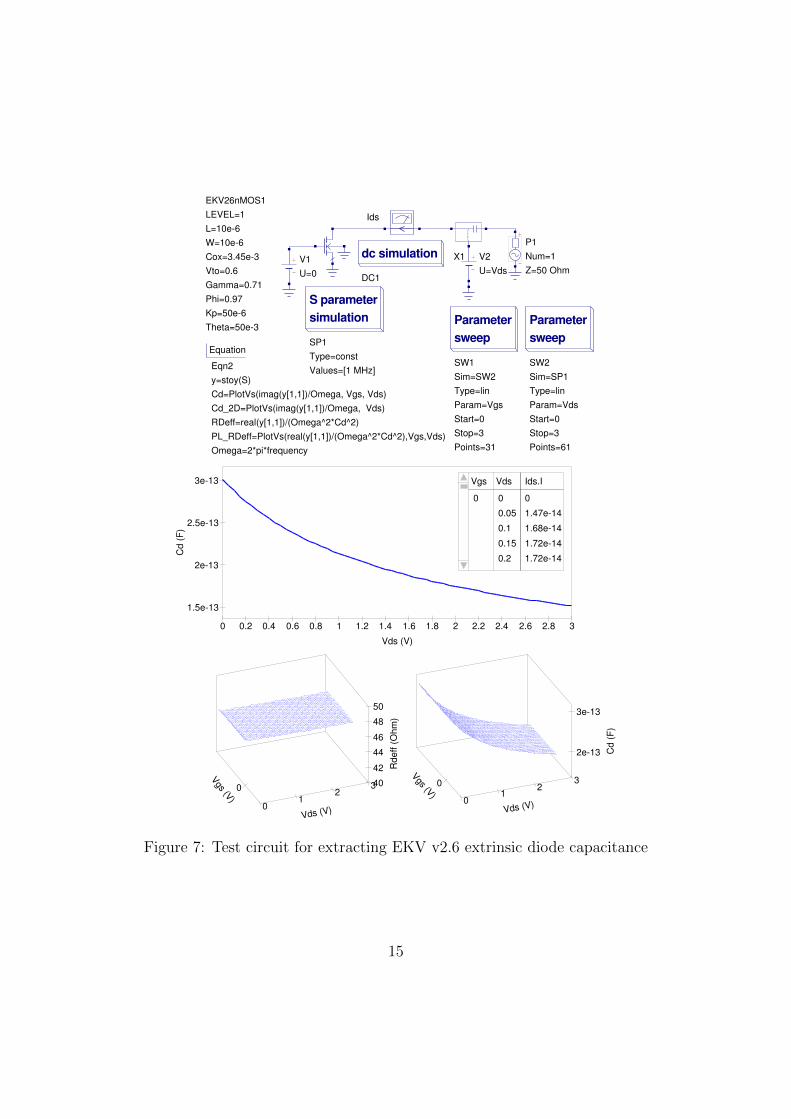
Extraction of extrinsic diode capacitance and drain resis-tance
The extrinsic section of the EKV v2.6 model includes diodes which in turn aremodelled by conventional DC characteristics and parallel capacitance. This ca-pacitance is represented by depletion layer capacitance in the diode reverse biasregion of operation. In the diode forward bias section of the I-V characteristicdiffusion capacitance dominates. Figure 7 illustrates a test circuit that allows thediode capacitance to be extracted as a function of Vds. In Fig. 7 the nMOS deviceis turned off and the drain to bulk diode reverse biased. Simple analysis indicatesthat
y11∼= ω2 ·RDeff ·Cd2 + j ·ω ·Cd, when ω ·RDeff ·Cd << 1. (25)
Hence, Cd = imag(y11/ω) and Rdeff = real(y11/(ω2 ·Cd2)), where ω = 2 ·π · f ,
f is the frequency of y-parameter measurement, and Cd is the diode capacitance.The data shown in Fig. 7 indicate good agreement with the expected values for Cdand RDeff ; which are expected to be Cd = 300fF at Vds=0V, and Rdeff = 46Ω.
Simulating EKV v2.6 MOSFET noise
The EKV v2.6 intrinsic device noise is modelled by a noise current source connectedbetween the internal drain and source terminals. The noise current source Idsn, seeFig. 1, is composed of a thermal noise component and a flicker noise component.The Power Spectral Density (SPSD) of these components are given by:
SPSD = Sthermal + Sflicker (26)
Where
12

X1
P1Num=1Z=50 Ohm
EKV26nMOS1LEVEL=1L=10e-6W=10e-6Cox=3.45e-3Vto=0.6Gamma=0.71Phi=0.97Kp=50e-6Theta=50e-3Cgso=1.5e-10Cgdo=1.5e-10Cgbo=4.0e-10Cj0=300e-15
V1U=Vgs
RgnR=1
dc simulation
DC1
Parametersweep
SW1Sim=SW2Type=linParam=VdsStart=0Stop=3Points=31
Ids_n V2U=Vds
Equation
Eqn1y=stoy(S)L=10e-6W=10e-6Cox=3.45e-3Cg=imag(y[1,1])/OmegaCgpl=PlotVs( Cg/(Cox*W*L), Vds, Vgs)Rg=PlotVs( (real(y[1,1])/(Omega*Omega*Cg*Cg)), Vds, Vgs)Cg_2D=PlotVs(Cg, Vgs)Omega=2*pi*frequency
S parametersimulation
SP1Type=constValues=[1 MHz]
Parametersweep
SW2Sim=SP1Type=linParam=VgsStart=-2Stop=2Points=201
-2 -1 0 1 2
Vgs (V)
0
2Vds (V
)
0.5
1
Cg/
(W*L
*Cox
)
-2 -1 0 1 21e-13
2e-13
3e-13
4e-13
Vgs (V)
Cg
(F)
-2 0 2
Vgs (V)
0
Vds (V
) 0
1
2
Rgn
(Ohm
)
Figure 5: y11 test circuit and values of Cg for the long channel EKV v2.6 nMOSmodel
13

X1
P1Num=1Z=50 Ohm
RgnR=1
dc simulation
DC1Ids_n
Equation
Eqn1y=stoy(S)L=10e-6W=10e-6Cox=3.45e-3Cg=imag(y[1,1])/OmegaCgpl=PlotVs( Cg/(Cox*W*L), Vds, Vgs)Rg=PlotVs( (real(y[1,1])/(Omega*Omega*Cg*Cg)), Vds, Vgs)Cg_2D=PlotVs(Cg, Vgs)Omega=2*pi*frequency
S parametersimulation
SP1Type=constValues=[1 MHz]
EKV26pMOS1L=10e-6W=20e-6Cox=3.45e-3Vto=-0.55Gamma=0.69Phi=0.87Kp=20e-6Theta=50e-3Cgso=1.5e-10Cgdo=1.5e-10Cgbo=4.0e-10Cj0=300e-15
V1U=Vgs
V2U=Vds
Parametersweep
SW1Sim=SW2Type=linParam=VdsStart=0Stop=-3Points=31
Parametersweep
SW2Sim=SP1Type=linParam=VgsStart=2Stop=-2Points=201
-2 -1 0 1 2
Vgs (V)
-2
0
Vds (V
)
1
2
Cg/
(W*L
*Cox
)
-2 -1 0 1 22e-13
4e-13
6e-13
8e-13
Vgs (V)
Cg
(F)
-2 0 2
Vgs (V)
0Vds (V
) 0
1
2
Rgn
(Ohm
)
Figure 6: y11 test circuit and values of Cg for the long channel EKV v2.6 pMOSmodel
14
Ids
X1 V2U=Vds
EKV26nMOS1LEVEL=1L=10e-6W=10e-6Cox=3.45e-3Vto=0.6Gamma=0.71Phi=0.97Kp=50e-6Theta=50e-3
dc simulation
DC1
S parametersimulation
SP1Type=constValues=[1 MHz]
P1Num=1Z=50 Ohm
V1U=0
Parametersweep
SW1Sim=SW2Type=linParam=VgsStart=0Stop=3Points=31
Equation
Eqn2y=stoy(S)Cd=PlotVs(imag(y[1,1])/Omega, Vgs, Vds)Cd_2D=PlotVs(imag(y[1,1])/Omega, Vds)RDeff=real(y[1,1])/(Omega^2*Cd^2)PL_RDeff=PlotVs(real(y[1,1])/(Omega^2*Cd^2),Vgs,Vds)Omega=2*pi*frequency
Parametersweep
SW2Sim=SP1Type=linParam=VdsStart=0Stop=3Points=61
0 0.2 0.4 0.6 0.8 1 1.2 1.4 1.6 1.8 2 2.2 2.4 2.6 2.8 3
1.5e-13
2e-13
2.5e-13
3e-13
Vds (V)
Cd (F)
01
23
Vds (V)
0
Vgs (V)
40
42
44
46
48
50
Rdeff (Ohm)
01
23
Vds (V)
0
Vgs (V)
2e-13
3e-13
Cd (F)
Vgs
0
Vds
0
0.05
0.1
0.15
0.2
Ids.I
0
1.47e-14
1.68e-14
1.72e-14
1.72e-14
Figure 7: Test circuit for extracting EKV v2.6 extrinsic diode capacitance
15

• Thermal noiseSthermal = 4 · k ·T · β · | qI | (27)
• Flicker noise
Sflicker =KF · g2
mg
Np ·Weff ·Ns ·Leff ·Cox · fAf, (28)
gmg =∂Ids
∂V gs= β ·V t ·
(√4 · If
Ispecific+ 1−
√4 · Ir
Ispecific+ 1
)(29)
Where β is a transconductance factor, qI = qD + qS, and the other symbols aredefined in the EKV v2.6 long channel parameter list or have their usual meaning.Noise has been implemented in both the Qucs long channel and short channelEKV v2.6 models. In addition to the intrinsic device noise the Qucs EKV v2.6model includes the thermal noise components for both extrinsic resistors RDeff andRSeff. Figure 8 presents a typical noise test circuit and simulated noise currents.In Figure 8 four nMOS devices are biased under different DC conditions and theirnoise current simulated for a range of W values between 1e-6 m and 100e-6 m.The first three devices include both thermal and flicker noise components (KF =1e-27) while the fourth device has it’s flicker component set to zero. The resultingcurrent noise curves clearly demonstrate the effect of summing intrinsic thermaland flicker components on the overall performance of the EKV v2.6 noise model.
16

Ids
Ids1
Ids2
V2U=3V
V4U=2 V
EKV26nMOS8L=1.0e-6W=WKf=1.0e-27Af=1.0
EKV26nMOS7L=1.0e-6W=WKf=1.0e-27Af=1.0
EKV26nMOS9L=1.0e-6W=WKf=1.0e-27Af=1.0
V1U=0.6
V3U=1
Ids3EKV26nMOS10L=1.0e-6W=WKf=0.0Af=1.0
dc simulation
DC1
ac simulation
AC1Type=logStart=100HzStop=100 MHzPoints=131Noise=yes
Parametersweep
SW1Sim=AC1Type=logParam=WStart=1e-6Stop=100e-6Points=11
100 1e3 1e4 1e5 1e6 1e7 1e81e-12
1e-11
1e-10
1e-9
1e-8
Frequency (Hz)
Idsn (A/sqrt(H
z))
Figure 8: Test circuit for simulating EKV v2.6 noise: Ids.in blue curve, Ids1.in redcurve, Ids2.in black curve and Ids3.in green curve
17

The Qucs short channel EKV v2.6 model
The Qucs implementation of the short short channel EKV v2.6 MOSFET modelcontains all the features implemented in the long channel version of the model plusa number of characteristics specific to short channel operation. However, the shortchannel version of the model does not use parameter Theta. Parameter LEVEL setto 2 selects the short channel model. Both pMOS and nMOS versions of the modelare available for both long and short channel implementations. The entire shortchannel EKV v2.6 MOSFET model is described by roughly 94 equations. Readerswho are interested in the mathematics of the model should consult “The EPFL-EKV MOSFET Model Equations for Simulation” publication cited in previoustext. Appendix A lists the complete Verilog-A code for the first release of theQucs EKV v2.6 MOSFET models. Additional Verilog-A code has been added tothe model equation code to (1) allow interchange of the drain and source terminals,and (2) select nMOS or pMOS devices.
Short channel model parameters (LEVEL = 2)
Name Symbol Description Unit Default nMOS Default pMOSLEVEL Model selector 2 2
L L length parameter m 10e− 6 10e− 6W W width parameter m 10e− 6 10e− 6Np Np parallel multiple device number 1 1Ns Ns series multiple device number 1 1
Cox Cox gate oxide capacitance per unit area F/m2 3.4e− 3 3.4e− 3Xj Xj metallurgical junction length m 0.15e− 6 0.15e− 6Dw Dw channel width correction m −0.02e− 6 −0.02e− 6Dl Dl channel length correction m −0.05e− 6 −0.05e− 6
Vto V to long channel threshold voltage V 0.5 −0.55
Gamma Gamma body effect parameter√V 0.7 0.69
Phi Phi bulk Fermi potential V 0.5 0.87Kp Kp transconductance parameter A/V 2 50e− 6 20e− 6EO EO mobility reduction coefficient V/m 88e− 6 51e− 6
Ucrit Ucrit longitudinal critical field V/m 4.5e− 6 18e− 6Lambda Lambda depletion length coefficient 0.23 1.1
Weta Weta narrow channel effect coefficient 0.05 0.0Leta eta short channel effect coefficient 0.28 0.45Q0 Q0 reverse short channel effect peak charge density 280e− 6 200e− 6Lk Lk reverse short channel effect characteristic length m 0.5e− 6 0.6e− 6Tcv Tcv threshold voltage temperature coefficient V/K 1.5e− 3 −1.4e− 3Bex Bex mobility temperature coefficient −1.5 −1.4Ucex Ucex longitudinal critical field temperature exponent 1.7 2.0Ibbt Ibbt temperature coefficient for Ibb 1/K 0.0 0.0Hdif Hdif heavily doped diffusion length m 0.9e− 6 0.9e− 6Rsh Rsh drain-source diffusion sheet resistance Ω/square 510 510Rsc Rsc source contact resistance Ω 0.0 0.0Rdc Rdc drain contact resistance Ω 0.0 0.0Cgso Cgso gate to source overlay capacitance F 1.5e− 10 1.5e− 10Cgdo Cgdo gate to drain overlay capacitance F 1.5e− 10 1.5e− 10Cgbo Cgbo gate to bulk overlay capacitance F 4e− 10 4e− 10
N N diode emission coefficient 1.0 1.0Is Is leakage current A 1e− 1 1e− 14
18
Name Symbol Description Unit Default nMOS Default pMOSBv Bv reverse breakdown voltage V 100 100Ibv Ibv current at Bv A 1e− 3 1e− 3Vj V j junction potential V 1.0 1.0Cj0 Cj0 zero bias depletion capacitance F 1e− 12 1e− 12M M grading coefficient 0.5 0.5
Area Area relative area 1.0 1.0Fc Fc forward-bias depletion capcitance coefficient 0.5 0.5Tt Tt transit time s 0.1e− 9 0.1e− 9Xti Xti saturation current temperature exponent 3.0 3.0Kf KF flicker noise coefficient 1e− 27 1e− 28Af Af flicker noise exponent 1.0 1.0
Avto Avto area related threshold mismatch parameter 0 0Akp Akp area related gain mismatch parameter 0 0
Agamma Agamma area related body effect mismatch parameter 0 0Iba Iba first impact ionization coefficient 1/m 2e8 0.0Ibb Ibb second impact ionization coefficient V/m 3.5e8 3.5e8Ibn Ibn saturation voltage factor for impact ionization 1.0 1.0
Tnom Tnom parameter measurement temperature C 26.85 26.85Temp Temp device temperature C 26.85 26.85
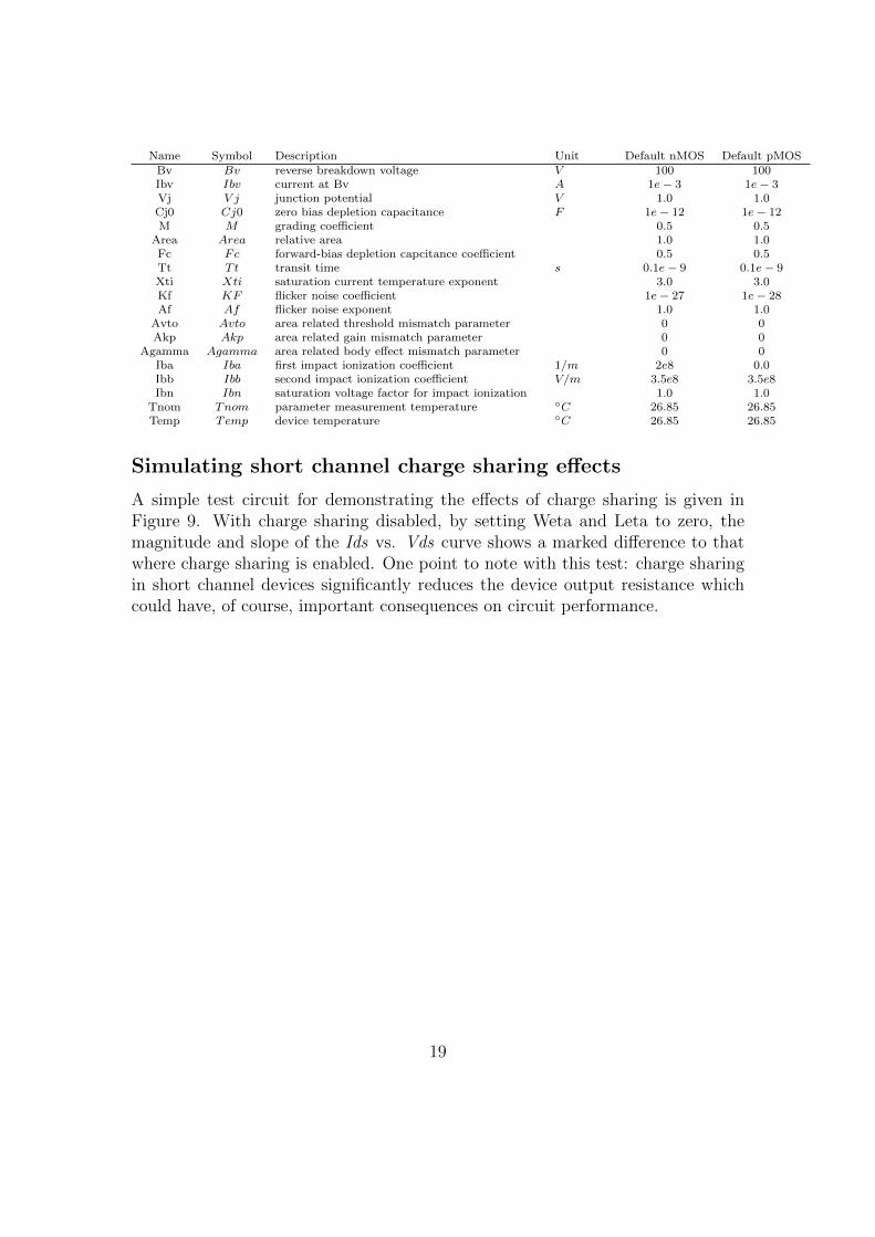
Simulating short channel charge sharing effects
A simple test circuit for demonstrating the effects of charge sharing is given inFigure 9. With charge sharing disabled, by setting Weta and Leta to zero, themagnitude and slope of the Ids vs. Vds curve shows a marked difference to thatwhere charge sharing is enabled. One point to note with this test: charge sharingin short channel devices significantly reduces the device output resistance whichcould have, of course, important consequences on circuit performance.
19

V2U=Vds
EKV26nMOS2LEVEL=2L=0.5e-6W=10e-6Cox=3.45e-3Xj=0.15e-6Dw=-0.02e-6Dl=-0.05e-6Vto=0.6Gamma=0.71Phi=0.97Kp=150e-6EO=88.0e6Ucrit=4.5e6Lambda=0.23Weta=0.05Leta=0.28Q0=280e-6Lk=0.5e-6
EKV26nMOS1LEVEL=2L=0.5e-6W=10e-6Cox=3.45e-3Xj=0.15e-6Dw=-0.02e-6Dl=-0.05e-6Vto=0.6Gamma=0.71Phi=0.97Kp=150e-6EO=88.0e6Ucrit=4.5e6Lambda=0.23Weta=0.0Leta=0.0Q0=280e-6Lk=0.5e-6
V1U=0.7
Parametersweep
SW1Sim=SW2Type=linParam=VgsStart=0Stop=3Points=7
dc simulation
DC1
Parametersweep
SW2Sim=DC1Type=linParam=VdsStart=0Stop=3.3Points=101
Ids_charge_Sharing
Ids_NO_Charge_Sharing
0 0.5 1 1.5 2 2.5 3
0
2e-6
4e-6
6e-6
8e-6
Vds (v)
Ids
(A)
Figure 9: Test circuit for simulating EKV v2.6 charge sharing effects in shortchannel devices: Ids blue curve; NO charge sharing (Weta = 0.0, Leta = 0.0), Idsred curve; charge sharing (Weta = 0.05, Leta = 0.28)
20

End note
This report outlines some of the background to the Qucs implementation of theEKV v2.6 MOSFET model. A series of test results demonstrate a range of resultsthat have been achieved with this new Qucs compact device model. Although thetest results give data similar to what is expected in all cases it must be stressedthat this is the first release of this MOSFET model and as such it will probablycontain bugs. A great deal of work has gone into providing this new Qucs model.However, all the effort has been worthwhile because for the first time Qucs nowhas a submicron MOSFET model. Please use the model and report bugs to theQucs development team. Much work still remains to be done in the developmentof MOSFET models for Qucs. In future releases both bug fixes and new modelsare likely to feature strongly. Once again I would like to thank Stefan Jahn andW ladys law Grabinski (of MOS-AK) for their encouragement and support duringthe period I have been working on developing the Qucs implementation of theEKV v2.6 model and writing this report.
Qucs Verilog-A code for the EKV v2.6 MOSFET
model
nMOS: EKV equation numbers are given on the right-handside of code lines
// Qucs EPFL−EKV 2.6 nMOS model ://// The s t r u c t u r e and t h e o r e t i c a l background to the EKV 2.6// Veri log−a model i s presented in the Qucs EPFL−EKV 2.6 repor t .// Typica l parameters are f o r 0.5um CMOS (C) EPLFL−LEG 1999.// Geometry range : Short channel W>= 0.8um, L >= 0.5um// Long channel W>= 2um, L >= 2um// Voltage range : |Vgb | < 3.3V, |Vdb | < 3.3V, |Vsb | < 2V//// This i s f r e e so f tware ; you can r e d i s t r i b u t e i t and/or modify// i t under the terms o f the GNU General Pub l i c License as pub l i s h ed by// the Free Software Foundation ; e i t h e r ver s ion 2 , or ( at your opt ion )// any l a t e r ver s ion .//// Copyright (C) , Mike Brinson , mbrin72043@yahoo . co . uk , May 2008.//‘ include ” d i s c i p l i n e s . vams”‘ include ”cons tant s . vams”
//module EKV26nMOS ( Drain , Gate , Source , Bulk ) ;inout Drain , Gate , Source , Bulk ;
e l e c t r i c a l Drain , Gate , Source , Bulk ;// In t e rna l nodese l e c t r i c a l Dra in int , Sou r c e in t ;
21

‘define a t t r ( txt ) (∗ txt ∗)// Device dimension parametersparameter real LEVEL = 1 from [ 1 : 2 ]
‘ a t t r ( i n f o=”long = 1 , shor t = 2 ” ) ;parameter real L = 0.5 e−6 from [ 0 . 0 : i n f ]
‘ a t t r ( i n f o=”length parameter ” un i t = ”m” ) ;parameter real W = 10e−6 from [ 0 . 0 : i n f ]
‘ a t t r ( i n f o=”Width parameter ” un i t = ”m” ) ;parameter real Np = 1.0 from [ 1 . 0 : i n f ]
‘ a t t r ( i n f o=” p a r a l l e l mu l t ip l e dev i c e number ” ) ;parameter real Ns = 1 .0 from [ 1 . 0 : i n f ]
‘ a t t r ( i n f o=” s e r i e s mu l t ip l e dev i c e number ” ) ;// Process parametersparameter real Cox = 3.45 e−3 from [ 0 : i n f ]
‘ a t t r ( i n f o=”gate oxide capac i tance per un i t area ” un i t = ”F/m∗∗2 ” ) ;parameter real Xj = 0.15 e−6 from [ 0 . 0 1 e−6 : 1 . 0 e−6]
‘ a t t r ( i n f o=” m e t a l l u r g i c a l j unc t i on depth ” un i t = ”m” ) ;parameter real Dw = −0.02e−6 from [− i n f : 0 . 0 ]
‘ a t t r ( i n f o=”channel width c o r r e c t i o n ” un i t = ”m” ) ;parameter real Dl = −0.05e−6 from [− i n f : 0 . 0 ]
‘ a t t r ( i n f o=”channel l ength c o r r e c t i o n ” un i t = ”m” ) ;// Basic i n t r i n s i c model parametersparameter real Vto = 0 .6 from [ 1 e−6 : 2 . 0 ]
‘ a t t r ( i n f o=”long channel th r e sho ld vo l tage ” un i t=”V” ) ;parameter real Gamma = 0.71 from [ 0 . 0 : 2 . 0 ]
‘ a t t r ( i n f o=”body e f f e c t parameter ” un i t=”V∗∗(1/2) ” ) ;parameter real Phi = 0.97 from [ 0 . 3 : 2 . 0 ]
‘ a t t r ( i n f o=”bulk Fermi p o t e n t i a l ” un i t=”V” ) ;parameter real Kp = 150e−6 from [10 e−6 : i n f ]
‘ a t t r ( i n f o=”transconductance parameter ” un i t = ”A/V∗∗2 ” ) ;parameter real Theta = 50e−3 from [ 0 . 0 : i n f ]
‘ a t t r ( i n f o=”mob i l i ty r educt i on c o e f f i c i e n t ” un i t = ”1/V” ) ;parameter real EO = 88.0 e6 from [ 1 . 0 e6 : i n f ]
‘ a t t r ( i n f o=”mob i l i ty c o e f f i c i e n t ” un i t=”V/m” ) ;parameter real Ucr i t = 4 .5 e6 from [ 2 . 0 e6 : 25 .0 e6 ]
‘ a t t r ( i n f o=” l o n g i t u d i n a l c r i t i c a l f i e l d ” un i t=”V/m” ) ;// Channel l eng t h and charge shar ing parametersparameter real Lambda = 0.23 from [ 0 . 1 : i n f ]
‘ a t t r ( i n f o=”d e p l e t i o n l ength c o e f f i c i e n t ” ) ;parameter real Weta = 0.05 from [ 0 . 0 : i n f ]
‘ a t t r ( i n f o=”narrow−channel e f f e c t c o e f f i c i e n t ” ) ;parameter real Leta = 0.28 from [ 0 . 0 : i n f ]
‘ a t t r ( i n f o=” l o n g i t u d i n a l c r i t i c a l f i e l d ” ) ;// Reverse shor t channel e f f e c t parametersparameter real Q0 = 280e−6 from [ 0 . 0 : i n f ]
‘ a t t r ( i n f o=”r e v e r s e shor t channel charge dens i ty ” un i t=”A∗ s /m∗∗2 ” ) ;parameter real Lk = 0.5 e−6 from [ 0 . 0 : i n f ]
‘ a t t r ( i n f o=” c h a r a c t e r i s t i c l ength ” un i t=”m” ) ;// I n t r i n s i c model temperature parametersparameter real Tcv = 1 .5 e−3
‘ a t t r ( i n f o=”thre sho ld vo l tage temperature c o e f f i c i e n t ” un i t=”V/K” ) ;parameter real Bex = −1.5
‘ a t t r ( i n f o=”mob i l i ty temperature c o e f f i c i e n t ” ) ;parameter real Ucex = 1 .7
‘ a t t r ( i n f o=”Long i tud ina l c r i t i c a l f i e l d temperature exponent ” ) ;parameter real Ibbt = 0 .0
‘ a t t r ( i n f o=”Ibb temperature c o e f f i c i e n t ” un i t=”1/K” ) ;// Ser i e s r e s i s t an c e c a l c u l a t i o n parametersparameter real Hdif = 0 .9 e−6 from [ 0 . 0 : i n f ]
‘ a t t r ( i n f o=”heav i l y doped d i f f u s i o n l ength ” un i t = ”m” ) ;parameter real Rsh = 510 .0 from [ 0 . 0 : i n f ]
‘ a t t r ( i n f o=”dra in / source d i f f u s i o n shee t r e s i s t a n c e ” un i t=”Ohm/ square ” ) ;
22

parameter real Rsc = 0 .0 from [ 0 . 0 : i n f ]‘ a t t r ( i n f o=”source contact r e s i s t a n c e ” un i t=”Ohm” ) ;
parameter real Rdc = 0 .0 from [ 0 . 0 : i n f ]‘ a t t r ( i n f o=”dra in contact r e s i s t a n c e ” un i t=”Ohm” ) ;
// Gate over lap capac i tancesparameter real Cgso = 1 .5 e−10 from [ 0 . 0 : i n f ]
‘ a t t r ( i n f o=”gate to source over lap capac i tance ” un i t = ”F/m” ) ;parameter real Cgdo = 1 .5 e−10 from [ 0 . 0 : i n f ]
‘ a t t r ( i n f o=”gate to dra in over lap capac i tance ” un i t= ”F/m” ) ;parameter real Cgbo = 4 .0 e−10 from [ 0 . 0 : i n f ]
‘ a t t r ( i n f o=”gate to bulk over lap capac i tance ” un i t= ”F/m” ) ;// Impact i on i z a t i on r e l a t e d parametersparameter real Iba = 2e8 from [ 0 . 0 : i n f ]
‘ a t t r ( i n f o=” f i r s t impact i o n i z a t i o n c o e f f i c i e n t ” un i t = ”1/m” ) ;parameter real Ibb = 3 .5 e8 from [ 1 . 0 e8 : i n f ]
‘ a t t r ( i n f o=”second impact i o n i z a t i o n c o e f f i c i e n t ” un i t=”V/m” ) ;parameter real Ibn = 1 .0 from [ 0 . 1 : i n f ]
‘ a t t r ( i n f o=”s a t u r a t i o n vo l tage f a c t o r f o r impact i o n i z a t i o n ” ) ;// F l i c k e r noise parametersparameter real Kf = 1 .0 e−27 from [ 0 . 0 : i n f ]
‘ a t t r ( i n f o=” f l i c k e r no i s e c o e f f i c i e n t ” ) ;parameter real Af = 1 .0 from [ 0 . 0 : i n f ]
‘ a t t r ( i n f o=” f l i c k e r no i s e exponent ” ) ;// Matching parametersparameter real Avto = 0 .0 from [ 0 . 0 : i n f ]
‘ a t t r ( i n f o=”area r e l a t e d thesho ld vo l tage mismatch parameter ” un i t = ”V∗m” ) ;parameter real Akp = 0.0 from [ 0 . 0 : i n f ]
‘ a t t r ( i n f o=”area r e l a t e d gain mismatch parameter ” un i t=”m” ) ;parameter real Agamma = 0.0 from [ 0 . 0 : i n f ]
‘ a t t r ( i n f o=”area r e l a t e d body e f f e c t mismatch parameter ” un i t=”s q r t (V)∗m” ) ;// Diode parametersparameter real N=1.0 from [ 1 e−6: i n f ]
‘ a t t r ( i n f o=”emis s ion c o e f f i c i e n t ” ) ;parameter real I s=1e−14 from [ 1 e−20: i n f ]
‘ a t t r ( i n f o=”s a t u r a t i o n cur rent ” un i t=”A” ) ;parameter real Bv=100 from [ 1 e−6: i n f ]
‘ a t t r ( i n f o=”r e v e r s e breakdown vo l tage ” un i t=”V” ) ;parameter real Ibv=1e−3 from [ 1 e−6: i n f ]
‘ a t t r ( i n f o=”cur rent at r e v e r s e breakdown vo l tage ” un i t=”A” ) ;parameter real Vj=1.0 from [ 1 e−6: i n f ]
‘ a t t r ( i n f o=”junc t i on p o t e n t i a l ” un i t=”V” ) ;parameter real Cj0=300e−15 from [ 0 : i n f ]
‘ a t t r ( i n f o=”zero−b ia s junc t i on capac i tance ” un i t=”F” ) ;parameter real M=0.5 from [ 1 e−6: i n f ]
‘ a t t r ( i n f o=”grading c o e f f i c i e n t ” ) ;parameter real Area=1.0 from [ 1 e−3: i n f ]
‘ a t t r ( i n f o=”diode r e l a t i v e area ” ) ;parameter real Fc=0.5 from [ 1 e−6: i n f ]
‘ a t t r ( i n f o=”forward−b ia s d e p l e t i o n capc i tance c o e f f i c i e n t ” ) ;parameter real Tt=0.1e−9 from [ 1 e−20: i n f ]
‘ a t t r ( i n f o=” t r a n s i t time ” un i t=”s ” ) ;parameter real Xti =3.0 from [ 1 e−6: i n f ]
‘ a t t r ( i n f o=”s a t u r a t i o n cur rent temperature exponent ” ) ;// Temperature parametersparameter real Tnom = 26.85
‘ a t t r ( i n f o=”parameter measurement temperature ” un i t = ”C e l s i u s ” ) ;// Local v a r i a b l e sreal e p s i l o n s i , eps i l onox , Tnomk, T2 , Tratio , Vto T , Ucrit T , Egnom , Eg , Phi T ;real Weff , Le f f , RDeff , RSeff , con1 , con2 , Vtoa , Kpa , Kpa T ,Gammaa, C eps i lon , x i ;real nnn , deltaV RSCE , Vg , Vs , Vd, Vgs , Vgd , Vds , Vdso2 , VG, VS, VD;real VGprime , VP0, VSprime , VDprime , Gamma0, Gammaprime , Vp;real n , X1 , i f f , X2 , i r , Vc , Vdss , Vdssprime , deltaV , Vip ;
23

real Lc , DeltaL , Lprime , Lmin , Leq , X3 , i rpr ime , Beta0 , eta ;real Qb0 , Beta0prime , nq , Xf , Xr , qD, qS , qI , qB , Beta , I s p e c i f i c , Ids , Vib , Idb , Ibb T ;real A, B, Vt T2 , Eg T1 , Eg T2 , Vj T2 , Cj0 T2 , F1 , F2 , F3 , Is T2 ;real Id1 , Id2 , Id3 , Id4 , Is1 , Is2 , Is3 , Is4 , V1 , V2 , Ib d , Ib s , Qd, Qs , Qd1 , Qd2 , Qs1 , Qs2 ;real qb , qg , qgso , qgdo , qgbo , fourkt , Sthermal , gm, S f l i c k e r , StoDswap , p n MOS ;//analog begin// Equation i n i t i a l i z a t i o np n MOS = 1 . 0 ; // nMOSA=7.02e−4;B=1108.0;e p s i l o n s i = 1.0359 e−10; // Eqn 4ep s i l onox = 3.453143 e−11; // Eqn 5Tnomk = Tnom+273.15; // Eqn 6T2=$temperature ;Trat io = T2/Tnomk ;Vto T = Vto−Tcv∗(T2−Tnomk ) ;Egnom = 1.16−0.000702∗Tnomk∗Tnomk/(Tnomk+1108);Eg = 1.16−0.000702∗T2∗T2/(T2+1108);Phi T = Phi∗Trat io − 3 .0∗ $vt∗ ln ( Trat io )−Egnom∗Trat io+Eg ;Ibb T = Ibb ∗(1.0+ Ibbt ∗(T2 −Tnomk ) ) ;Weff = W + Dw; // Eqn 25L e f f = L + Dl ; // Eqn 26RDeff = ( ( Hdif ∗Rsh)/ Weff )/Np + Rdc ;RSef f = ( ( Hdif ∗Rsh)/ Weff )/Np + Rsc ;con1 = s q r t (Np∗Weff∗Ns∗ L e f f ) ;Vt T2=‘P K∗T2/‘P Q ;Eg T1=Eg−A∗Tnomk∗Tnomk/(B+Tnomk ) ;Eg T2=Eg−A∗T2∗T2/(B+T2 ) ;Vj T2=(T2/Tnomk)∗Vj−(2∗Vt T2 )∗ ln (pow ( (T2/Tnomk) ,1 . 5 ) ) − ( (T2/Tnomk)∗Eg T1−Eg T2 ) ;Cj0 T2=Cj0∗(1+M∗(400 e−6∗(T2−Tnomk)−(Vj T2−Vj )/ Vj ) ) ;F1=(Vj/(1−M))∗(1−pow((1−Fc) ,(1−M) ) ) ;F2=pow((1−Fc ) , (1+M) ) ;F3=1−Fc∗(1+M) ;Is T2=I s ∗pow( (T2/Tnomk) , ( Xti /N))∗ l imexp ((−Eg T1/Vt T2)∗(1−T2/Tnomk ) ) ;con2 = (Cox∗Ns∗Np∗Weff∗ L e f f ) ;f ou rk t = 4.0∗ ‘P K∗T2 ;//i f (LEVEL == 2)begin
Ucrit T = Ucr i t ∗pow( Tratio , Ucex ) ;Vtoa = Vto+Avto/con1 ; // Eqn 27Kpa = Kp∗(1.0+Akp/con1 ) ; // Eqn 28Kpa T = Kpa∗pow( Tratio , Bex ) ; // Eqn 18Gammaa = Gamma+Agamma/con1 ; // Eqn 29C eps i l on = 4.0∗pow(22 e−3, 2 ) ; // Eqn 30x i = 0 . 0 2 8∗ ( 1 0 . 0∗ ( L e f f /Lk) −1 .0) ; // Eqn 31nnn = 1.0+0.5∗ ( x i+ s q r t (pow( xi , 2 ) + C eps i l on ) ) ;deltaV RSCE = (2 . 0∗Q0/Cox )∗ ( 1 . 0 / pow(nnn , 2 ) ) ; // Eqn 32
end//// Model branch and node v o l t a g e s//
Vg = p n MOS∗V( Gate , Bulk ) ;Vs = p n MOS∗V( Source , Bulk ) ;Vd = p n MOS∗V( Drain , Bulk ) ;VG=Vg ; // Eqn 22i f ( (Vd−Vs) >= 0 . 0 )
beginStoDswap = 1 . 0 ;VS=Vs ; // Eqn 23
24

VD=Vd; // Eqn 24end
elsebegin
StoDswap = −1.0;VD=Vs ;VS=Vd;
endi f (LEVEL == 2)
VGprime=VG−Vto T−deltaV RSCE+Phi T+Gamma∗ s q r t ( Phi T ) ; // Eqn 33 nMOS equat ionelse
VGprime=Vg−Vto T+Phi T+Gamma∗ s q r t ( Phi T ) ;
//i f (LEVEL == 2)begini f (VGprime > 0)
VP0=VGprime−Phi T−Gammaa∗( s q r t (VGprime+(Gammaa/ 2 . 0 )∗ (Gammaa/ 2 . 0 ) )−(Gammaa/ 2 . 0 ) ) ; // Eqn 34
elseVP0 = −Phi T ;
VSprime =0.5∗(VS+Phi T+s q r t (pow( (VS+Phi T ) , 2 ) + pow( (4 . 0∗ $vt ) , 2 ) ) ) ; // Eqn 35VDprime=0.5∗(VD+Phi T+s q r t (pow( (VD+Phi T ) , 2 ) + pow( (4 . 0∗ $vt ) , 2 ) ) ) ; // Eqn 35Gamma0=Gammaa−( e p s i l o n s i /Cox )∗ ( ( Leta/ L e f f )∗ ( s q r t ( VSprime)+ s q r t (VDprime ) )
−(3.0∗Weta/Weff )∗ s q r t (VP0+Phi T ) ) ; // Eqn 36Gammaprime = 0 . 5∗ (Gamma0+s q r t ( pow(Gamma0, 2 ) +0.1∗ $vt ) ) ; // Eqn 37i f (VGprime > 0 .0 )
Vp = VGprime−Phi T−Gammaprime∗( s q r t (VGprime+(Gammaprime/2 .0 )∗(Gammaprime / 2 . 0 ) ) − (Gammaprime / 2 . 0 ) ) ; // Eqn 38
elseVp = −Phi T ;
n = 1 .0 +Gammaa/(2 . 0∗ s q r t (Vp+Phi T+4.0∗ $vt ) ) ; // Eqn 39end
elsebegini f (VGprime > 0)
Vp=VGprime−Phi T−Gamma∗( s q r t (VGprime+(Gamma/ 2 . 0 )∗ (Gamma/ 2 . 0 ) )−(Gamma/ 2 . 0 ) ) ; // Eqn 34
elseVp = −Phi T ;
n = 1 .0 +Gamma/(2 . 0∗ s q r t (Vp+Phi T+4.0∗ $vt ) ) ; // Eqn 39end//X1 = (Vp−VS)/ $vt ;i f f = ln (1.0+ limexp (X1/ 2 . 0 ) )∗ ln (1.0+ limexp (X1 / 2 . 0 ) ) ; // Eqn 44X2 = (Vp−VD)/ $vt ;i r = ln (1.0+ limexp (X2/ 2 . 0 ) )∗ ln (1.0+ limexp (X2 / 2 . 0 ) ) ; // Eqn 57//i f (LEVEL == 2)begin
Vc = Ucrit T ∗Ns∗ L e f f ; // Eqn 45Vdss = Vc∗( s q r t ( 0 .25 + ( ( $vt /(Vc) )∗ s q r t ( i f f ) ) ) −0 . 5 ) ; // Eqn 46;Vdssprime = Vc∗( s q r t ( 0 .25 + ( $vt /Vc)∗ ( s q r t ( i f f )−0.75∗ ln ( i f f ) ) ) − 0 . 5 )
+$vt ∗( ln (Vc/(2 . 0∗ $vt ) ) − 0 .6 ) ; // Eqn 47i f (Lambda∗( s q r t ( i f f ) > ( Vdss/ $vt ) ) )
deltaV = 4.0∗ $vt∗ s q r t (Lambda∗( s q r t ( i f f ) −(Vdss/ $vt ) )+ ( 1 . 0 / 6 4 . 0 ) ) ; // Eqn 48
elsedeltaV = 1 . 0 / 6 4 . 0 ;
Vdso2 = (VD−VS) / 2 . 0 ; // Eqn 49Vip = s q r t ( pow( Vdss , 2) + pow( deltaV , 2 ) ) − s q r t ( pow( ( Vdso2 − Vdss ) , 2)
+ pow ( deltaV , 2 ) ) ; // Eqn 50
25

Lc = s q r t ( ( e p s i l o n s i /Cox)∗Xj ) ; // Eqn 51DeltaL = Lambda∗Lc∗ ln (1 .0+(( Vdso2−Vip )/( Lc∗Ucrit T ) ) ) ; // Eqn 52Lprime = Ns∗ L e f f − DeltaL + ( ( Vdso2+Vip )/ Ucrit T ) ; // Eqn 53Lmin = Ns∗ L e f f / 1 0 . 0 ; // Eqn 54Leq = 0 .5∗ ( Lprime + s q r t ( pow( Lprime , 2) + pow(Lmin , 2 ) ) ) ; // Eqn 55X3 = (Vp−Vdso2−VS−s q r t ( pow( Vdssprime , 2) + pow( deltaV , 2 ) )
+ s q r t ( pow( ( Vdso2−Vdssprime ) , 2) + pow( deltaV , 2 ) ) ) / $vt ;i rp r ime = ln (1.0+ limexp (X3/ 2 . 0 ) )∗ ln (1.0+ limexp (X3 / 2 . 0 ) ) ; // Eqn 56Beta0 = Kpa T∗(Np∗Weff/Leq ) ; // Eqn 58eta = 0 . 5 ; // Eqn 59 − nMOSQb0 = Gammaa∗ s q r t ( Phi T ) ; // Eqn 60;Beta0prime = Beta0 ∗ ( 1 . 0 +(Cox/(EO∗ e p s i l o n s i ) )∗Qb0 ) ; // Eqn 61nq = 1 .0 +Gammaa/(2 . 0∗ s q r t (Vp+Phi T+1e−6)) ; // Eqn 69
endelsenq = 1 .0 +Gamma/(2 . 0∗ s q r t (Vp+Phi T+1e−6)) ; // Eqn 69
//Xf = s q r t (0.25+ i f f ) ; // Eqn 70Xr = s q r t (0.25+ i r ) ; // Eqn 71qD = −nq∗( ( 4 . 0 / 1 5 . 0 ) ∗ ( ( 3 . 0 ∗pow( Xr , 3 ) + 6 .0∗pow( Xr , 2)∗Xf + 4.0∗Xr∗pow( Xf , 2)
+ 2 .0∗pow( Xf , 3 ) ) / ( pow( ( Xf+Xr ) , 2) ) ) −0.5) ; // Eqn 72qS = −nq∗( ( 4 . 0 / 1 5 . 0 ) ∗ ( ( 3 . 0 ∗pow( Xf , 3 ) + 6 .0∗pow( Xf , 2)∗Xr + 4.0∗Xf∗pow( Xr , 2)
+ 2 .0∗pow(Xr , 3 ) ) / ( pow( ( Xf+Xr ) , 2) ) ) −0.5) ; // Eqn 73qI = −nq∗( ( 4 . 0 / 3 . 0 ) ∗ ( (pow( Xf ,2)+( Xf∗Xr)+pow(Xr , 2 ) ) / ( Xf+Xr ) ) − 1 . 0 ) ; // Eqn 74i f (LEVEL == 2)
i f (VGprime > 0)qB = (−Gammaa∗ s q r t (Vp+Phi T+1e−6))∗(1 .0/ $vt ) − ( (nq−1.0)/nq )∗ qI ; // Eqn 75
elseqB = −VGprime/ $vt ;
elsei f (VGprime > 0)
qB = (−Gamma∗ s q r t (Vp+Phi T+1e−6))∗(1 .0/ $vt ) − ( (nq−1.0)/nq )∗ qI ; // Eqn 75else
qB = −VGprime/ $vt ;//i f (LEVEL == 2)
Beta = Beta0prime / (1 . 0 + (Cox/ (EO∗ e p s i l o n s i ) )∗ $vt∗abs (qB+eta ∗qI ) ) ; // Eqn 62else
Beta = Kp∗( Weff/ L e f f )/(1+Theta∗Vp ) ;//I s p e c i f i c = 2 .0∗n∗Beta∗pow( $vt , 2 ) ; // Eqn 65//i f (LEVEL == 2)
beginIds = I s p e c i f i c ∗( i f f −i rp r ime ) ; // Eqn 66Vib = VD−VS−Ibn ∗2 .0∗Vdss ; // Eqn 67i f ( Vib > 0 . 0 )Idb = Ids ∗( Iba /Ibb T )∗Vib∗exp ( (−Ibb T∗Lc )/ Vib ) ; // Eqn 68
elseIdb = 0 . 0 ;
endelse
Ids = I s p e c i f i c ∗( i f f − i r ) ; // Eqn 66//Sthermal = fourk t ∗Beta∗abs ( qI ) ;gm = Beta∗$vt ∗( s q r t ( ( 4 . 0∗ i f f / I s p e c i f i c ) +1.0) − s q r t ( ( 4 . 0∗ i r / I s p e c i f i c ) + 1 . 0 ) ) ;S f l i c k e r = ( Kf∗gm∗gm)/(Np∗Weff∗Ns∗ L e f f ∗Cox ) ;//qb = con2∗$vt∗qB ;qg = con2∗$vt∗(−qI−qB ) ;qgso = Cgso∗Weff∗Np∗(VG−VS ) ;qgdo = Cgdo∗Weff∗Np∗(VG−VD) ;
26

qgbo = Cgbo∗ L e f f ∗Np∗VG;// Drain and source d iodesi f ( StoDswap > 0 . 0 )
beginV1=p n MOS∗V( Bulk , Dra in in t ) ;V2=p n MOS∗V( Bulk , Sou r c e in t ) ;
endelse
beginV2=p n MOS∗V( Bulk , Dra in in t ) ;V1=p n MOS∗V( Bulk , Sou r c e in t ) ;
endId1= (V1>−5.0∗N∗$vt ) ? Area∗ Is T2 ∗( l imexp ( V1/(N∗Vt T2 ) )−1.0) : 0 ;Qd1=(V1<Fc∗Vj )? Tt∗ Id1+Area ∗( Cj0 T2∗Vj T2/(1−M))∗(1−pow((1−V1/Vj T2 ) ,(1−M) ) ) : 0 ;Id2=(V1<=−5.0∗N∗$vt ) ? −Area∗ Is T2 : 0 ;Qd2=(V1>=Fc∗Vj )? Tt∗ Id1+Area∗Cj0 T2 ∗(F1+(1/F2 )∗ ( F3∗(V1−Fc∗Vj T2)+(M/(2 .0∗Vj T2 ) )
∗(V1∗V1−Fc∗Fc∗Vj T2∗Vj T2 ) ) ) : 0 ;Id3=(V1 == −Bv) ? −Ibv : 0 ;Id4=(V1<−Bv) ?−Area∗ Is T2 ∗( l imexp (−(Bv+V1)/ Vt T2)−1.0+Bv/Vt T2 ) : 0 ;Ib d = Id1+Id2+Id3+Id4 ;Qd = Qd1+Qd2 ;//I s 1= (V2>−5.0∗N∗$vt ) ? Area∗ Is T2 ∗( l imexp ( V2/(N∗Vt T2 ) )−1.0) : 0 ;Qs1=(V2<Fc∗Vj )? Tt∗ I s 1+Area ∗( Cj0 T2∗Vj T2/(1−M))∗(1−pow((1−V2/Vj T2 ) ,(1−M) ) ) : 0 ;I s 2 =(V2<=−5.0∗N∗$vt ) ? −Area∗ Is T2 : 0 ;Qs2=(V2>=Fc∗Vj )? Tt∗ I s 1+Area∗Cj0 T2 ∗(F1+(1/F2 )∗ ( F3∗(V2−Fc∗Vj T2)+(M/(2 .0∗Vj T2 ) )
∗(V2∗V2−Fc∗Fc∗Vj T2∗Vj T2 ) ) ) : 0 ;I s 3 =(V2 == −Bv) ? −Ibv : 0 ;I s 4 =(V2<−Bv) ?−Area∗ Is T2 ∗( l imexp (−(Bv+V2)/ Vt T2)−1.0+Bv/Vt T2 ) : 0 ;I b s = I s1+I s2+I s3+I s4 ;Qs = Qs1+Qs2 ;// Current and noise con t r i b u t i on si f ( StoDswap > 0 . 0 )begin
i f ( RDeff > 0 . 0 )I ( Drain , Dra in in t ) <+ V( Drain , Dra in in t )/ RDeff ;
elseI ( Drain , Dra in in t ) <+ V( Drain , Dra in in t )/1 e−7;
i f ( RSef f > 0 . 0 )I ( Source , Sou r c e in t ) <+ V( Source , Sou r c e in t )/ RSef f ;
elseI ( Source , Sou r c e in t ) <+ V( Source , Sou r c e in t )/1 e−7;
I ( Dra in int , Sou r c e in t ) <+ p n MOS∗ Ids ;i f (LEVEL == 2)
I ( Dra in int , Bulk ) <+ p n MOS∗ Idb ;I ( Gate , Dra in in t ) <+ p n MOS∗0 .5∗ ddt ( qg ) ;I ( Gate , Sou r c e in t ) <+ p n MOS∗0 .5∗ ddt ( qg ) ;I ( Dra in int , Bulk ) <+ p n MOS∗0 .5∗ ddt ( qb ) ;I ( Source int , Bulk ) <+ p n MOS∗0 .5∗ ddt ( qb ) ;I ( Gate , Sou r c e in t ) <+ p n MOS∗ddt ( qgso ) ;I ( Gate , Dra in in t ) <+ p n MOS∗ddt ( qgdo ) ;I ( Gate , Bulk ) <+ p n MOS∗ddt ( qgbo ) ;I ( Bulk , Dra in in t ) <+ p n MOS∗ Ib d ;I ( Bulk , Dra in in t ) <+ p n MOS∗ddt (Qd) ;I ( Bulk , Sou r c e in t ) <+ p n MOS∗ I b s ;I ( Bulk , Sou r c e in t ) <+ p n MOS∗ddt (Qs ) ;I ( Dra in int , Sou r c e in t ) <+ whi t e no i s e ( Sthermal , ”thermal ” ) ;I ( Dra in int , Sou r c e in t ) <+ f l i c k e r n o i s e ( S f l i c k e r , Af , ” f l i c k e r ” ) ;I ( Drain , Dra in in t ) <+ whi t e no i s e ( f ou rk t /RDeff , ”thermal ” ) ;I ( Source , Sou r c e in t ) <+ whi t e no i s e ( f ou rk t / RSeff , ”thermal ” ) ;
endelse
27

begini f ( RSef f > 0 . 0 )
I ( Drain , Dra in in t ) <+ V( Drain , Dra in in t )/ RSef f ;else
I ( Drain , Dra in in t ) <+ V( Drain , Dra in in t )/1 e−7;i f ( RDeff > 0 . 0 )
I ( Source , Sou r c e in t ) <+ V( Source , Sou r c e in t )/ RDeff ;else
I ( Source , Sou r c e in t ) <+ V( Source , Sou r c e in t )/1 e−7;I ( Source int , Dra in in t ) <+ p n MOS∗ Ids ;i f (LEVEL == 2)
I ( Source int , Bulk ) <+ p n MOS∗ Idb ;I ( Gate , Sou r c e in t ) <+ p n MOS∗0 .5∗ ddt ( qg ) ;I ( Gate , Dra in in t ) <+ p n MOS∗0 .5∗ ddt ( qg ) ;I ( Source int , Bulk ) <+ p n MOS∗0 .5∗ ddt ( qb ) ;I ( Dra in int , Bulk ) <+ p n MOS∗0 .5∗ ddt ( qb ) ;I ( Gate , Dra in in t ) <+ p n MOS∗ddt ( qgso ) ;I ( Gate , Sou r c e in t ) <+ p n MOS∗ddt ( qgdo ) ;I ( Gate , Bulk ) <+ p n MOS∗ddt ( qgbo ) ;I ( Bulk , Sou r c e in t ) <+ p n MOS∗ Ib d ;I ( Bulk , Sou r c e in t ) <+ p n MOS∗ddt (Qd) ;I ( Bulk , Dra in in t ) <+ p n MOS∗ I b s ;I ( Bulk , Dra in in t ) <+ p n MOS∗ddt (Qs ) ;I ( Source int , Dra in in t ) <+ whi t e no i s e ( Sthermal , ”thermal ” ) ;I ( Source int , Dra in in t ) <+ f l i c k e r n o i s e ( S f l i c k e r , Af , ” f l i c k e r ” ) ;I ( Source int , Source ) <+ whi t e no i s e ( f ou rk t /RDeff , ”thermal ” ) ;I ( Dra in int , Drain ) <+ whi t e no i s e ( f ou rk t / RSeff , ”thermal ” ) ;
endendendmodule
pMOS: EKV equation numbers are given on the right-handside of code lines
// Qucs EPFL−EKV 2.6 pMOS model ://// The s t r u c t u r e and t h e o r e t i c a l background to the EKV 2.6// Veri log−a model i s presented in the Qucs EPL−EKV 2.6 repor t .// Typica l parameters are f o r 0.5um CMOS (C) EPLFL−LEG 1999.// Geometry range : Short channel : W>= 0.8um, L >= 0.5um// Long channel : W>= 2um, L >= 2um// Voltage range : |Vgb | < 3.3V, |Vdb | < 3.3V, |Vsb | < 2V//// This i s f r e e so f tware ; you can r e d i s t r i b u t e i t and/or modify// i t under the terms o f the GNU General Pub l i c License as pub l i s h ed by// the Free Software Foundation ; e i t h e r ver s ion 2 , or ( at your opt ion )// any l a t e r ver s ion .//// Copyright (C) , Mike Brinson , mbrin72043@yahoo . co . uk , May 2008.//‘ include ” d i s c i p l i n e s . vams”‘ include ”cons tant s . vams”
//module EKV26pMOS ( Drain , Gate , Source , Bulk ) ;inout Drain , Gate , Source , Bulk ;
e l e c t r i c a l Drain , Gate , Source , Bulk ;// In t e rna l nodese l e c t r i c a l Dra in int , Sou r c e in t ;‘define a t t r ( txt ) (∗ txt ∗)
28

// Device dimension parametersparameter real LEVEL = 1 from [ 1 : 2 ]
‘ a t t r ( i n f o=”long = 1 , shor t = 2 ” ) ;parameter real L = 0.5 e−6 from [ 0 . 0 : i n f ]
‘ a t t r ( i n f o=”length parameter ” un i t = ”m” ) ;parameter real W = 10e−6 from [ 0 . 0 : i n f ]
‘ a t t r ( i n f o=”Width parameter ” un i t = ”m” ) ;parameter real Np = 1.0 from [ 1 . 0 : i n f ]
‘ a t t r ( i n f o=” p a r a l l e l mu l t ip l e dev i c e number ” ) ;parameter real Ns = 1 .0 from [ 1 . 0 : i n f ]
‘ a t t r ( i n f o=” s e r i e s mu l t ip l e dev i c e number ” ) ;// Process parametersparameter real Cox = 3.45 e−3 from [ 0 : i n f ]
‘ a t t r ( i n f o=”gate oxide capac i tance per un i t area ” un i t = ”F/m∗∗2 ” ) ;parameter real Xj = 0.15 e−6 from [ 0 . 0 1 e−6 : 1 . 0 e−6]
‘ a t t r ( i n f o=” m e t a l l u r g i c a l j unc t i on depth ” un i t = ”m” ) ;parameter real Dw = −0.03e−6 from [− i n f : 0 . 0 ]
‘ a t t r ( i n f o=”channel width c o r r e c t i o n ” un i t = ”m” ) ;parameter real Dl = −0.05e−6 from [− i n f : 0 . 0 ]
‘ a t t r ( i n f o=”channel l ength c o r r e c t i o n ” un i t = ”m” ) ;// Basic i n t r i n s i c model parametersparameter real Vto = −0.55 from [− i n f : −1e−6]
‘ a t t r ( i n f o=”long channel th r e sho ld vo l tage ” un i t=”V” ) ;parameter real Gamma = 0.69 from [ 0 . 0 : 2 . 0 ]
‘ a t t r ( i n f o=”body e f f e c t parameter ” un i t=”V∗∗(1/2) ” ) ;parameter real Phi = 0.87 from [ 0 . 3 : 2 . 0 ]
‘ a t t r ( i n f o=”bulk Fermi p o t e n t i a l ” un i t=”V” ) ;parameter real Kp = 35e−6 from [10 e−6 : i n f ]
‘ a t t r ( i n f o=”transconductance parameter ” un i t = ”A/V∗∗2 ” ) ;parameter real Theta = 50e−3 from [ 0 . 0 : i n f ]
‘ a t t r ( i n f o=”mob i l i ty r educt i on c o e f f i c i e n t ” un i t = ”1/V” ) ;parameter real EO = 51.0 e6 from [ 1 . 0 e6 : i n f ]
‘ a t t r ( i n f o=”mob i l i ty c o e f f i c i e n t ” un i t=”V/m” ) ;parameter real Ucr i t = 18 .0 e6 from [ 2 . 0 e6 : 25 .0 e6 ]
‘ a t t r ( i n f o=” l o n g i t u d i n a l c r i t i c a l f i e l d ” un i t=”V/m” ) ;// Channel l eng t h and charge shar ing parametersparameter real Lambda = 1 .1 from [ 0 . 1 : i n f ]
‘ a t t r ( i n f o=”d e p l e t i o n l ength c o e f f i c i e n t ” ) ;parameter real Weta = 0 .0 from [ 0 . 0 : i n f ]
‘ a t t r ( i n f o=”narrow−channel e f f e c t c o e f f i c i e n t ” ) ;parameter real Leta = 0.45 from [ 0 . 0 : i n f ]
‘ a t t r ( i n f o=” l o n g i t u d i n a l c r i t i c a l f i e l d ” ) ;// Reverse shor t channel e f f e c t parametersparameter real Q0 = 200e−6 from [ 0 . 0 : i n f ]
‘ a t t r ( i n f o=”r e v e r s e shor t channel charge dens i ty ” un i t=”A∗ s /m∗∗2 ” ) ;parameter real Lk = 0.6 e−6 from [ 0 . 0 : i n f ]
‘ a t t r ( i n f o=” c h a r a c t e r i s t i c l ength ” un i t=”m” ) ;// I n t r i n s i c model temperature parametersparameter real Tcv = −1.4e−3
‘ a t t r ( i n f o=”thre sho ld vo l tage temperature c o e f f i c i e n t ” un i t=”V/K” ) ;parameter real Bex = −1.4
‘ a t t r ( i n f o=”mob i l i ty temperature c o e f f i c i e n t ” ) ;parameter real Ucex = 2 .0
‘ a t t r ( i n f o=”Long i tud ina l c r i t i c a l f i e l d temperature exponent ” ) ;parameter real Ibbt = 0 .0
‘ a t t r ( i n f o=”Ibb temperature c o e f f i c i e n t ” un i t = ”1/K” ) ;// Ser i e s r e s i s t an c e c a l c u l a t i o n parametersparameter real Hdif = 0 .9 e−6 from [ 0 . 0 : i n f ]
‘ a t t r ( i n f o=”heav i l y doped d i f f u s i o n l ength ” un i t = ”m” ) ;parameter real Rsh = 990 .0 from [ 0 . 0 : i n f ]
‘ a t t r ( i n f o=”dra in / source d i f f u s i o n shee t r e s i s t a n c e ” un i t=”Ohm/ square ” ) ;parameter real Rsc = 0 .0 from [ 0 . 0 : i n f ]
29

‘ a t t r ( i n f o=”source contact r e s i s t a n c e ” un i t=”Ohm” ) ;parameter real Rdc = 0 .0 from [ 0 . 0 : i n f ]
‘ a t t r ( i n f o=”dra in contact r e s i s t a n c e ” un i t=”Ohm” ) ;// Gate over lap capac i tancesparameter real Cgso = 1 .5 e−10 from [ 0 . 0 : i n f ]
‘ a t t r ( i n f o=”gate to source over lap capac i tance ” un i t = ”F/m” ) ;parameter real Cgdo = 1 .5 e−10 from [ 0 . 0 : i n f ]
‘ a t t r ( i n f o=”gate to dra in over lap capac i tance ” un i t= ”F/m” ) ;parameter real Cgbo = 4 .0 e−10 from [ 0 . 0 : i n f ]
‘ a t t r ( i n f o=”gate to bulk over lap capac i tance ” un i t= ”F/m” ) ;// Impact i on i z a t i on r e l a t e d parametersparameter real Iba = 0 .0 from [ 0 . 0 : i n f ]
‘ a t t r ( i n f o=” f i r s t impact i o n i z a t i o n c o e f f i c i e n t ” un i t = ”1/m” ) ;parameter real Ibb = 3 .0 e8 from [ 1 . 0 e8 : i n f ]
‘ a t t r ( i n f o=”second impact i o n i z a t i o n c o e f f i c i e n t ” un i t=”V/m” ) ;parameter real Ibn = 1 .0 from [ 0 . 1 : i n f ]
‘ a t t r ( i n f o=”s a t u r a t i o n vo l tage f a c t o r f o r impact i o n i z a t i o n ” ) ;// F l i c k e r noise parametersparameter real Kf = 1 .0 e−28 from [ 0 . 0 : i n f ]
‘ a t t r ( i n f o=” f l i c k e r no i s e c o e f f i c i e n t ” ) ;parameter real Af = 1 .0 from [ 0 . 0 : i n f ]
‘ a t t r ( i n f o=” f l i c k e r no i s e exponent ” ) ;// Matching parametersparameter real Avto = 0 .0 from [ 0 . 0 : i n f ]
‘ a t t r ( i n f o=”area r e l a t e d thesho ld vo l tage mismatch parameter ” un i t = ”V∗m” ) ;parameter real Akp = 0.0 from [ 0 . 0 : i n f ]
‘ a t t r ( i n f o=”area r e l a t e d gain mismatch parameter ” un i t=”m” ) ;parameter real Agamma = 0.0 from [ 0 . 0 : i n f ]
‘ a t t r ( i n f o=”area r e l a t e d body e f f e c t mismatch parameter ” un i t=”s q r t (V)∗m” ) ;// Diode parametersparameter real N=1.0 from [ 1 e−6: i n f ]
‘ a t t r ( i n f o=”emis s ion c o e f f i c i e n t ” ) ;parameter real I s=1e−14 from [ 1 e−20: i n f ]
‘ a t t r ( i n f o=”s a t u r a t i o n cur rent ” un i t=”A” ) ;parameter real Bv=100 from [ 1 e−6: i n f ]
‘ a t t r ( i n f o=”r e v e r s e breakdown vo l tage ” un i t=”V” ) ;parameter real Ibv=1e−3 from [ 1 e−6: i n f ]
‘ a t t r ( i n f o=”cur rent at r e v e r s e breakdown vo l tage ” un i t=”A” ) ;parameter real Vj=1.0 from [ 1 e−6: i n f ]
‘ a t t r ( i n f o=”junc t i on p o t e n t i a l ” un i t=”V” ) ;parameter real Cj0=300e−15 from [ 0 : i n f ]
‘ a t t r ( i n f o=”zero−b ia s junc t i on capac i tance ” un i t=”F” ) ;parameter real M=0.5 from [ 1 e−6: i n f ]
‘ a t t r ( i n f o=”grading c o e f f i c i e n t ” ) ;parameter real Area=1.0 from [ 1 e−3: i n f ]
‘ a t t r ( i n f o=”diode r e l a t i v e area ” ) ;parameter real Fc=0.5 from [ 1 e−6: i n f ]
‘ a t t r ( i n f o=”forward−b ia s d e p l e t i o n capc i tance c o e f f i c i e n t ” ) ;parameter real Tt=0.1e−9 from [ 1 e−20: i n f ]
‘ a t t r ( i n f o=” t r a n s i t time ” un i t=”s ” ) ;parameter real Xti =3.0 from [ 1 e−6: i n f ]
‘ a t t r ( i n f o=”s a t u r a t i o n cur rent temperature exponent ” ) ;// Temperature parametersparameter real Tnom = 26.85
‘ a t t r ( i n f o=”parameter measurement temperature ” un i t = ”C e l s i u s ” ) ;// Local v a r i a b l e sreal e p s i l o n s i , eps i l onox , Tnomk, T2 , Tratio , Vto T , Ucrit T , Egnom , Eg , Phi T ;real Weff , Le f f , RDeff , RSeff , con1 , con2 , Vtoa , Kpa , Kpa T ,Gammaa, C eps i lon , x i ;real nnn , deltaV RSCE , Vg , Vs , Vd, Vgs , Vgd , Vds , Vdso2 , VG, VS, VD;real VGprime , VP0, VSprime , VDprime , Gamma0, Gammaprime , Vp;real n , X1 , i f f , X2 , i r , Vc , Vdss , Vdssprime , deltaV , Vip ;real Lc , DeltaL , Lprime , Lmin , Leq , X3 , i rpr ime , Beta0 , eta ;
30
real Qb0 , Beta0prime , nq , Xf , Xr , qD, qS , qI , qB , Beta , I s p e c i f i c , Ids , Vib , Idb , Ibb T ;real A, B, Vt T2 , Eg T1 , Eg T2 , Vj T2 , Cj0 T2 , F1 , F2 , F3 , Is T2 ;real Id1 , Id2 , Id3 , Id4 , Is1 , Is2 , Is3 , Is4 , V1 , V2 , Ib d , Ib s , Qd, Qs , Qd1 , Qd2 , Qs1 , Qs2 ;real qb , qg , qgso , qgdo , qgbo , fourkt , Sthermal , gm, S f l i c k e r , StoDswap , p n MOS ;//analog begin// Equation i n i t i a l i z a t i o np n MOS = −1.0; // pMOSA=7.02e−4;B=1108.0;e p s i l o n s i = 1.0359 e−10; // Eqn 4ep s i l onox = 3.453143 e−11; // Eqn 5Tnomk = Tnom+273.15; // Eqn 6T2=$temperature ;Trat io = T2/Tnomk ;Vto T = −Vto+Tcv∗(T2−Tnomk ) ; // Signs o f Vto and Tcv changed fo r pMOSEgnom = 1.16−0.000702∗Tnomk∗Tnomk/(Tnomk+1108);Eg = 1.16−0.000702∗T2∗T2/(T2+1108);Phi T = Phi∗Trat io − 3 .0∗ $vt∗ ln ( Trat io )−Egnom∗Trat io+Eg ;Ibb T = Ibb ∗(1.0+ Ibbt ∗(T2 −Tnomk ) ) ;Weff = W + Dw; // Eqn 25L e f f = L + Dl ; // Eqn 26RDeff = ( ( Hdif ∗Rsh)/ Weff )/Np + Rdc ;RSef f = ( ( Hdif ∗Rsh)/ Weff )/Np + Rsc ;con1 = s q r t (Np∗Weff∗Ns∗ L e f f ) ;Vt T2=‘P K∗T2/‘P Q ;Eg T1=Eg−A∗Tnomk∗Tnomk/(B+Tnomk ) ;Eg T2=Eg−A∗T2∗T2/(B+T2 ) ;Vj T2=(T2/Tnomk)∗Vj−(2∗Vt T2 )∗ ln (pow ( (T2/Tnomk) ,1 . 5 ) ) − ( (T2/Tnomk)∗Eg T1−Eg T2 ) ;Cj0 T2=Cj0∗(1+M∗(400 e−6∗(T2−Tnomk)−(Vj T2−Vj )/ Vj ) ) ;F1=(Vj/(1−M))∗(1−pow((1−Fc) ,(1−M) ) ) ;F2=pow((1−Fc ) , (1+M) ) ;F3=1−Fc∗(1+M) ;Is T2=I s ∗pow( (T2/Tnomk) , ( Xti /N))∗ l imexp ((−Eg T1/Vt T2)∗(1−T2/Tnomk ) ) ;con2 = (Cox∗Ns∗Np∗Weff∗ L e f f ) ;f ou rk t = 4.0∗ ‘P K∗T2 ;//i f (LEVEL == 2)begin
Ucrit T = Ucr i t ∗pow( Tratio , Ucex ) ;Vtoa = Vto+Avto/con1 ; // Eqn 27Kpa = Kp∗(1.0+Akp/con1 ) ; // Eqn 28Kpa T = Kpa∗pow( Tratio , Bex ) ; // Eqn 18Gammaa = Gamma+Agamma/con1 ; // Eqn 29C eps i l on = 4.0∗pow(22 e−3, 2 ) ; // Eqn 30x i = 0 . 0 2 8∗ ( 1 0 . 0∗ ( L e f f /Lk) −1 .0) ; // Eqn 31nnn = 1.0+0.5∗ ( x i+ s q r t (pow( xi , 2 ) + C eps i l on ) ) ;deltaV RSCE = (2 . 0∗Q0/Cox )∗ ( 1 . 0 / pow(nnn , 2 ) ) ; // Eqn 32
end//// Model branch and node v o l t a g e s//
Vg = p n MOS∗V( Gate , Bulk ) ;Vs = p n MOS∗V( Source , Bulk ) ;Vd = p n MOS∗V( Drain , Bulk ) ;VG=Vg ; // Eqn 22i f ( (Vd−Vs) >= 0 . 0 )
beginStoDswap = 1 . 0 ;VS=Vs ; // Eqn 23VD=Vd; // Eqn 24
31

endelse
beginStoDswap = −1.0;VD=Vs ;VS=Vd;
endi f (LEVEL == 2)
VGprime=VG−Vto T−deltaV RSCE+Phi T+Gamma∗ s q r t ( Phi T ) ; // Eqn 33 nMOS equat ionelse
VGprime=Vg−Vto T+Phi T+Gamma∗ s q r t ( Phi T ) ;
i f (LEVEL == 2)begini f (VGprime > 0)
VP0=VGprime−Phi T−Gammaa∗( s q r t (VGprime+(Gammaa/ 2 . 0 )∗ (Gammaa/2.0))−(Gammaa/ 2 . 0 ) ) ;// Eqn 34
elseVP0 = −Phi T ;
VSprime =0.5∗(VS+Phi T+s q r t (pow( (VS+Phi T ) , 2 ) + pow( (4 . 0∗ $vt ) , 2 ) ) ) ; // Eqn 35VDprime=0.5∗(VD+Phi T+s q r t (pow( (VD+Phi T ) , 2 ) + pow( (4 . 0∗ $vt ) , 2 ) ) ) ; // Eqn 35Gamma0=Gammaa−( e p s i l o n s i /Cox )∗ ( ( Leta/ L e f f )∗ ( s q r t ( VSprime)+ s q r t (VDprime ) )
−(3.0∗Weta/Weff )∗ s q r t (VP0+Phi T ) ) ; // Eqn 36Gammaprime = 0 . 5∗ (Gamma0+s q r t ( pow(Gamma0, 2 ) +0.1∗ $vt ) ) ; // Eqn 37i f (VGprime > 0 .0 )
Vp = VGprime−Phi T−Gammaprime∗( s q r t (VGprime+(Gammaprime / 2 . 0 )∗ ( Gammaprime / 2 . 0 ) )− (Gammaprime / 2 . 0 ) ) ; // Eqn 38
elseVp = −Phi T ;
n = 1 .0 +Gammaa/(2 . 0∗ s q r t (Vp+Phi T+4.0∗ $vt ) ) ; // Eqn 39end
elsebegini f (VGprime > 0)
Vp=VGprime−Phi T−Gamma∗( s q r t (VGprime+(Gamma/ 2 . 0 )∗ (Gamma/2.0))−(Gamma/ 2 . 0 ) ) ;// Eqn 34
elseVp = −Phi T ;
n = 1 .0 +Gamma/(2 . 0∗ s q r t (Vp+Phi T+4.0∗ $vt ) ) ; // Eqn 39end//X1 = (Vp−VS)/ $vt ;i f f = ln (1.0+ limexp (X1/ 2 . 0 ) )∗ ln (1.0+ limexp (X1 / 2 . 0 ) ) ; // Eqn 44X2 = (Vp−VD)/ $vt ;i r = ln (1.0+ limexp (X2/ 2 . 0 ) )∗ ln (1.0+ limexp (X2 / 2 . 0 ) ) ; // Eqn 57//i f (LEVEL == 2)beginVc = Ucrit T ∗Ns∗ L e f f ; // Eqn 45Vdss = Vc∗( s q r t ( 0 .25 + ( ( $vt /(Vc) )∗ s q r t ( i f f ) ) ) −0 . 5 ) ; // Eqn 46;Vdssprime = Vc∗( s q r t ( 0 .25 + ( $vt /Vc)∗ ( s q r t ( i f f )−0.75∗ ln ( i f f ) ) ) − 0 . 5 )
+$vt ∗( ln (Vc/(2 . 0∗ $vt ) ) − 0 .6 ) ; // Eqn 47i f (Lambda∗( s q r t ( i f f ) > ( Vdss/ $vt ) ) )
deltaV = 4.0∗ $vt∗ s q r t (Lambda∗( s q r t ( i f f ) −(Vdss/ $vt ) ) + ( 1 . 0 / 6 4 . 0 ) ) ; // Eqn 48else deltaV = 1 . 0 / 6 4 . 0 ;Vdso2 = (VD−VS) / 2 . 0 ; // Eqn 49Vip = s q r t ( pow( Vdss , 2) + pow( deltaV , 2 ) ) − s q r t ( pow( ( Vdso2 − Vdss ) , 2)
+ pow ( deltaV , 2 ) ) ; // Eqn 50Lc = s q r t ( ( e p s i l o n s i /Cox)∗Xj ) ; // Eqn 51DeltaL = Lambda∗Lc∗ ln (1 .0+(( Vdso2−Vip )/( Lc∗Ucrit T ) ) ) ; // Eqn 52Lprime = Ns∗ L e f f − DeltaL + ( ( Vdso2+Vip )/ Ucrit T ) ; // Eqn 53Lmin = Ns∗ L e f f / 1 0 . 0 ; // Eqn 54
32

Leq = 0 .5∗ ( Lprime + s q r t ( pow( Lprime , 2) + pow(Lmin , 2 ) ) ) ; // Eqn 55X3 = (Vp−Vdso2−VS−s q r t ( pow( Vdssprime , 2) + pow( deltaV , 2 ) )
+ s q r t ( pow( ( Vdso2−Vdssprime ) , 2) + pow( deltaV , 2 ) ) ) / $vt ;i rp r ime = ln (1.0+ limexp (X3/ 2 . 0 ) )∗ ln (1.0+ limexp (X3 / 2 . 0 ) ) ; // Eqn 56Beta0 = Kpa T∗(Np∗Weff/Leq ) ; // Eqn 58eta = 0 .3333333 ; // Eqn 59 − pMOSQb0 = Gammaa∗ s q r t ( Phi T ) ; // Eqn 60;Beta0prime = Beta0 ∗ ( 1 . 0 +(Cox/(EO∗ e p s i l o n s i ) )∗Qb0 ) ; // Eqn 61nq = 1 .0 +Gammaa/(2 . 0∗ s q r t (Vp+Phi T+1e−6)) ; // Eqn 69
endelse
nq = 1 .0 +Gamma/(2 . 0∗ s q r t (Vp+Phi T+1e−6)) ; // Eqn 69//Xf = s q r t (0.25+ i f f ) ; // Eqn 70Xr = s q r t (0.25+ i r ) ; // Eqn 71qD = −nq∗( ( 4 . 0 / 1 5 . 0 ) ∗ ( ( 3 . 0 ∗pow( Xr , 3 ) + 6 .0∗pow( Xr , 2)∗Xf + 4.0∗Xr∗pow( Xf , 2)
+ 2 .0∗pow( Xf , 3 ) ) / ( pow( ( Xf+Xr ) , 2) ) ) −0.5) ; // Eqn 72qS = −nq∗( ( 4 . 0 / 1 5 . 0 ) ∗ ( ( 3 . 0 ∗pow( Xf , 3 ) + 6 .0∗pow( Xf , 2)∗Xr + 4.0∗Xf∗pow( Xr , 2)
+ 2 .0∗pow(Xr , 3 ) ) / ( pow( ( Xf+Xr ) , 2) ) ) −0.5) ; // Eqn 73qI = −nq∗( ( 4 . 0 / 3 . 0 ) ∗ ( (pow( Xf ,2)+( Xf∗Xr)+pow(Xr , 2 ) ) / ( Xf+Xr ) ) − 1 . 0 ) ; // Eqn 74i f (LEVEL == 2)
i f (VGprime > 0)qB = (−Gammaa∗ s q r t (Vp+Phi T+1e−6))∗(1 .0/ $vt ) − ( (nq−1.0)/nq )∗ qI ; // Eqn 75
elseqB = −VGprime/ $vt ;
elsei f (VGprime > 0)
qB = (−Gamma∗ s q r t (Vp+Phi T+1e−6))∗(1 .0/ $vt ) − ( (nq−1.0)/nq )∗ qI ; // Eqn 75else
qB = −VGprime/ $vt ;//i f (LEVEL == 2)
Beta = Beta0prime / (1 . 0 + (Cox/ (EO∗ e p s i l o n s i ) )∗ $vt∗abs (qB+eta ∗qI ) ) ; // Eqn 62else
Beta = Kp∗( Weff/ L e f f )/(1+Theta∗Vp ) ;//I s p e c i f i c = 2 .0∗n∗Beta∗pow( $vt , 2 ) ; // Eqn 65//i f (LEVEL == 2)
beginIds = I s p e c i f i c ∗( i f f −i rp r ime ) ; // Eqn 66Vib = VD−VS−Ibn ∗2 .0∗Vdss ; // Eqn 67i f ( Vib > 0 . 0 )
Idb = Ids ∗( Iba /Ibb T )∗Vib∗exp ( (−Ibb T∗Lc )/ Vib ) ; // Eqn 68else
Idb = 0 . 0 ;end
elseIds = I s p e c i f i c ∗( i f f − i r ) ; // Eqn 66
//Sthermal = fourk t ∗Beta∗abs ( qI ) ;gm = Beta∗$vt ∗( s q r t ( ( 4 . 0∗ i f f / I s p e c i f i c ) +1.0) − s q r t ( ( 4 . 0∗ i r / I s p e c i f i c ) + 1 . 0 ) ) ;S f l i c k e r = ( Kf∗gm∗gm)/(Np∗Weff∗Ns∗ L e f f ∗Cox ) ;//qb = con2∗$vt∗qB ;qg = con2∗$vt∗(−qI−qB ) ;qgso = Cgso∗Weff∗Np∗(VG−VS ) ;qgdo = Cgdo∗Weff∗Np∗(VG−VD) ;qgbo = Cgbo∗ L e f f ∗Np∗VG;// Drain and source d iodesi f ( StoDswap > 0 . 0 )
begin
33

V1=p n MOS∗V( Bulk , Dra in in t ) ;V2=p n MOS∗V( Bulk , Sou r c e in t ) ;
endelse
beginV2=p n MOS∗V( Bulk , Dra in in t ) ;V1=p n MOS∗V( Bulk , Sou r c e in t ) ;
endId1= (V1>−5.0∗N∗$vt ) ? Area∗ Is T2 ∗( l imexp ( V1/(N∗Vt T2 ) )−1.0) : 0 ;Qd1=(V1<Fc∗Vj )? Tt∗ Id1+Area ∗( Cj0 T2∗Vj T2/(1−M))∗(1−pow((1−V1/Vj T2 ) ,(1−M) ) ) : 0 ;Id2=(V1<=−5.0∗N∗$vt ) ? −Area∗ Is T2 : 0 ;Qd2=(V1>=Fc∗Vj )? Tt∗ Id1+Area∗Cj0 T2 ∗(F1+(1/F2 )∗ ( F3∗(V1−Fc∗Vj T2)+(M/(2 .0∗Vj T2 ) )
∗(V1∗V1−Fc∗Fc∗Vj T2∗Vj T2 ) ) ) : 0 ;Id3=(V1 == −Bv) ? −Ibv : 0 ;Id4=(V1<−Bv) ?−Area∗ Is T2 ∗( l imexp (−(Bv+V1)/ Vt T2)−1.0+Bv/Vt T2 ) : 0 ;Ib d = Id1+Id2+Id3+Id4 ;Qd = Qd1+Qd2 ;//I s 1= (V2>−5.0∗N∗$vt ) ? Area∗ Is T2 ∗( l imexp ( V2/(N∗Vt T2 ) )−1.0) : 0 ;Qs1=(V2<Fc∗Vj )? Tt∗ I s 1+Area ∗( Cj0 T2∗Vj T2/(1−M))∗(1−pow((1−V2/Vj T2 ) ,(1−M) ) ) : 0 ;I s 2 =(V2<=−5.0∗N∗$vt ) ? −Area∗ Is T2 : 0 ;Qs2=(V2>=Fc∗Vj )? Tt∗ I s 1+Area∗Cj0 T2 ∗(F1+(1/F2 )∗ ( F3∗(V2−Fc∗Vj T2)+(M/(2 .0∗Vj T2 ) )
∗(V2∗V2−Fc∗Fc∗Vj T2∗Vj T2 ) ) ) : 0 ;I s 3 =(V2 == −Bv) ? −Ibv : 0 ;I s 4 =(V2<−Bv) ?−Area∗ Is T2 ∗( l imexp (−(Bv+V2)/ Vt T2)−1.0+Bv/Vt T2 ) : 0 ;I b s = I s1+I s2+I s3+I s4 ;Qs = Qs1+Qs2 ;// Current con t r i b u t i on si f ( StoDswap > 0 . 0 )begin
i f ( RDeff > 0 . 0 )I ( Drain , Dra in in t ) <+ V( Drain , Dra in in t )/ RDeff ;
elseI ( Drain , Dra in in t ) <+ V( Drain , Dra in in t )/1 e−7;
i f ( RSef f > 0 . 0 )I ( Source , Sou r c e in t ) <+ V( Source , Sou r c e in t )/ RSef f ;
elseI ( Source , Sou r c e in t ) <+ V( Source , Sou r c e in t )/1 e−7;
I ( Dra in int , Sou r c e in t ) <+ p n MOS∗ Ids ;i f (LEVEL == 2)
I ( Dra in int , Bulk ) <+ p n MOS∗ Idb ;I ( Gate , Dra in in t ) <+ p n MOS∗0 .5∗ ddt ( qg ) ;I ( Gate , Sou r c e in t ) <+ p n MOS∗0 .5∗ ddt ( qg ) ;I ( Dra in int , Bulk ) <+ p n MOS∗0 .5∗ ddt ( qb ) ;I ( Source int , Bulk ) <+ p n MOS∗0 .5∗ ddt ( qb ) ;I ( Gate , Sou r c e in t ) <+ p n MOS∗ddt ( qgso ) ;I ( Gate , Dra in in t ) <+ p n MOS∗ddt ( qgdo ) ;I ( Gate , Bulk ) <+ p n MOS∗ddt ( qgbo ) ;I ( Bulk , Dra in in t ) <+ p n MOS∗ Ib d ;I ( Bulk , Dra in in t ) <+ p n MOS∗ddt (Qd) ;I ( Bulk , Sou r c e in t ) <+ p n MOS∗ I b s ;I ( Bulk , Sou r c e in t ) <+ p n MOS∗ddt (Qs ) ;I ( Dra in int , Sou r c e in t ) <+ whi t e no i s e ( Sthermal , ”thermal ” ) ;I ( Dra in int , Sou r c e in t ) <+ f l i c k e r n o i s e ( S f l i c k e r , Af , ” f l i c k e r ” ) ;I ( Drain , Dra in in t ) <+ whi t e no i s e ( f ou rk t /RDeff , ”thermal ” ) ;I ( Source , Sou r c e in t ) <+ whi t e no i s e ( f ou rk t / RSeff , ”thermal ” ) ;
endelsebegin
i f ( RSef f > 0 . 0 )I ( Drain , Dra in in t ) <+ V( Drain , Dra in in t )/ RSef f ;
else
34

I ( Drain , Dra in in t ) <+ V( Drain , Dra in in t )/1 e−7;i f ( RDeff > 0 . 0 )
I ( Source , Sou r c e in t ) <+ V( Source , Sou r c e in t )/ RDeff ;else
I ( Source , Sou r c e in t ) <+ V( Source , Sou r c e in t )/1 e−7;I ( Source int , Dra in in t ) <+ p n MOS∗ Ids ;i f (LEVEL == 2)
I ( Source int , Bulk ) <+ p n MOS∗ Idb ;I ( Gate , Sou r c e in t ) <+ p n MOS∗0 .5∗ ddt ( qg ) ;I ( Gate , Dra in in t ) <+ p n MOS∗0 .5∗ ddt ( qg ) ;I ( Source int , Bulk ) <+ p n MOS∗0 .5∗ ddt ( qb ) ;I ( Dra in int , Bulk ) <+ p n MOS∗0 .5∗ ddt ( qb ) ;I ( Gate , Dra in in t ) <+ p n MOS∗ddt ( qgso ) ;I ( Gate , Sou r c e in t ) <+ p n MOS∗ddt ( qgdo ) ;I ( Gate , Bulk ) <+ p n MOS∗ddt ( qgbo ) ;I ( Bulk , Sou r c e in t ) <+ p n MOS∗ Ib d ;I ( Bulk , Sou r c e in t ) <+ p n MOS∗ddt (Qd) ;I ( Bulk , Dra in in t ) <+ p n MOS∗ I b s ;I ( Bulk , Dra in in t ) <+ p n MOS∗ddt (Qs ) ;I ( Source int , Dra in in t ) <+ whi t e no i s e ( Sthermal , ”thermal ” ) ;I ( Source int , Dra in in t ) <+ f l i c k e r n o i s e ( S f l i c k e r , Af , ” f l i c k e r ” ) ;I ( Source int , Source ) <+ whi t e no i s e ( f ou rk t /RDeff , ”thermal ” ) ;I ( Dra in int , Drain ) <+ whi t e no i s e ( f ou rk t / RSeff , ”thermal ” ) ;
endendendmodule
35

Update number one: September 2008
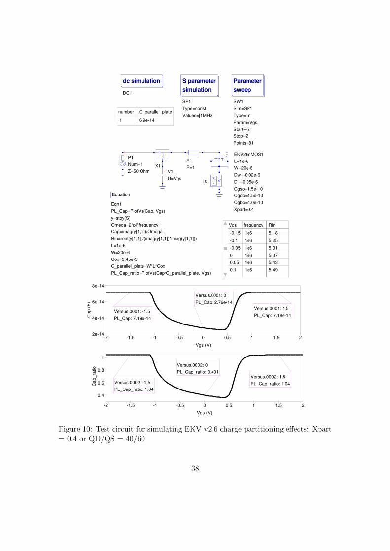
The first version of the Qucs EPFL-EKV v2.6 model provided Qucs users withreasonably complete long and short channel models for nMOS and pMOS devices.In no respect were these models optimized for minimum simulation run time orwere they flexible enough to allow users to select the style of charge partitioningemployed by the EKV model. Recent work on the Qucs implementation of theEKV v2.6 MOSFET model and the Qucs ADMS/XML interface has resulted in asignificant reduction in simulation run time overhead, particularly in transient andsmall signal analysis. The addition of a SPICE BSIM style partition parameterXpart to the Qucs version of the EKV v2.6 model now allows users to set thestyle of charge partitioning employed by the EKV model. These notes explain thefunction of the first EKV v2.6 update and introduce a series of test simulationsthat demonstrate the effects these changes have on the operation of the Qucs portof the EKV V2.6 model.
Model initialisation
Readers who have looked through the EKV v2.6 Verilog-A code listed in the pre-vious sections of these notes will probably have been struck by the quantity ofcalculations involved each time the code is evaluated during simulation. In thecase of transient analysis it is calculated at least once per time step, often re-sulting in many thousands of passes through the code. The more MOS devicesincluded in a circuit the greater the time overhead becomes. Obviously, a sensibleapproach would be to minimize the amount of calculation by only evaluating oncethose parts of the EKV model equations which result in constant values duringsimulation. The Verilog-A hardware description language provides a model ini-tialisation feature which selects those parts of a device model code which are tobe evaluated prior to the start of a simulation. The resulting calculated variablesare then available for use by other sections of the Verilog-A model code duringsimulation. In transient and small signal analysis this is particularly important asit significantly reduces simulation calculation time. Verilog-A employs the “at” (@(initial_step) or @(initial_model) ) language construction coupled with abegin ... end block to signify the Verilog-A code that is to be evaluated only atmodel initialisation. Although this technique does greatly improve model simula-tion speed it does imply significantly more work for the model developer in thatthe Verilog-A device code has to be split into initialisation and dynamic simulationsections. Readers interested in the detail of how this split can be achieved shouldcompare the latest EKV v2.6 Verilog-A CVS code given at the Qucs Web site withthat presented in previous sections of these notes.
36
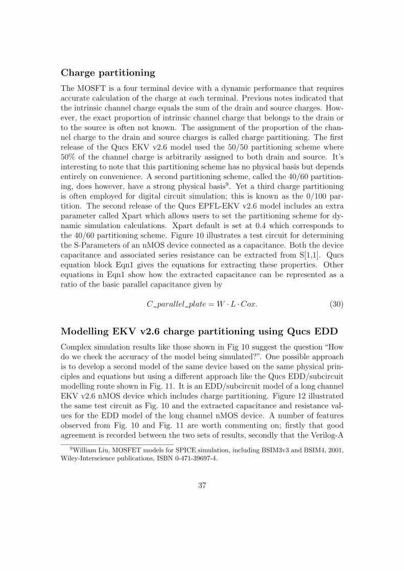
Charge partitioning
The MOSFT is a four terminal device with a dynamic performance that requiresaccurate calculation of the charge at each terminal. Previous notes indicated thatthe intrinsic channel charge equals the sum of the drain and source charges. How-ever, the exact proportion of intrinsic channel charge that belongs to the drain orto the source is often not known. The assignment of the proportion of the chan-nel charge to the drain and source charges is called charge partitioning. The firstrelease of the Qucs EKV v2.6 model used the 50/50 partitioning scheme where50% of the channel charge is arbitrarily assigned to both drain and source. It’sinteresting to note that this partitioning scheme has no physical basis but dependsentirely on convenience. A second partitioning scheme, called the 40/60 partition-ing, does however, have a strong physical basis9. Yet a third charge partitioningis often employed for digital circuit simulation; this is known as the 0/100 par-tition. The second release of the Qucs EPFL-EKV v2.6 model includes an extraparameter called Xpart which allows users to set the partitioning scheme for dy-namic simulation calculations. Xpart default is set at 0.4 which corresponds tothe 40/60 partitioning scheme. Figure 10 illustrates a test circuit for determiningthe S-Parameters of an nMOS device connected as a capacitance. Both the devicecapacitance and associated series resistance can be extracted from S[1,1]. Qucsequation block Eqn1 gives the equations for extracting these properties. Otherequations in Eqn1 show how the extracted capacitance can be represented as aratio of the basic parallel capacitance given by
C_parallel_plate = W ·L ·Cox. (30)
Modelling EKV v2.6 charge partitioning using Qucs EDD
Complex simulation results like those shown in Fig 10 suggest the question “Howdo we check the accuracy of the model being simulated?”. One possible approachis to develop a second model of the same device based on the same physical prin-ciples and equations but using a different approach like the Qucs EDD/subcircuitmodelling route shown in Fig. 11. It is an EDD/subcircuit model of a long channelEKV v2.6 nMOS device which includes charge partitioning. Figure 12 illustratedthe same test circuit as Fig. 10 and the extracted capacitance and resistance val-ues for the EDD model of the long channel nMOS device. A number of featuresobserved from Fig. 10 and Fig. 11 are worth commenting on; firstly that goodagreement is recorded between the two sets of results, secondly that the Verilog-A
9William Liu, MOSFET models for SPICE simulation, including BSIM3v3 and BSIM4, 2001,Wiley-Interscience publications, ISBN 0-471-39697-4.
37
Is
X1
P1Num=1Z=50 Ohm V1
U=Vgs
R1R=1
Equation
Eqn1PL_Cap=PlotVs(Cap, Vgs)y=stoy(S)Omega=2*pi*frequencyCap=imag(y[1,1])/OmegaRin=real(y[1,1])/(imag(y[1,1])*imag(y[1,1]))L=1e-6W=20e-6Cox=3.45e-3C_parallel_plate=W*L*CoxPL_Cap_ratio=PlotVs(Cap/C_parallel_plate, Vgs)
EKV26nMOS1L=1e-6W=20e-6Dw=-0.02e-6Dl=-0.05e-6Cgso=1.5e-10Cgdo=1.5e-10Cgbo=4.0e-10Xpart=0.4
Parametersweep
SW1Sim=SP1Type=linParam=VgsStart=-2Stop=2Points=81
S parametersimulation
SP1Type=constValues=[1MHz]
dc simulation
DC1
-2 -1.5 -1 -0.5 0 0.5 1 1.5 22e-14
4e-14
6e-14
8e-14
Vgs (V)
Cap
(F)
Versus.0001: 0PL_Cap: 2.76e-14Versus.0001: 0PL_Cap: 2.76e-14
Versus.0001: -1.5PL_Cap: 7.19e-14Versus.0001: -1.5PL_Cap: 7.19e-14
Versus.0001: 1.5PL_Cap: 7.18e-14Versus.0001: 1.5PL_Cap: 7.18e-14
-2 -1.5 -1 -0.5 0 0.5 1 1.5 2
0.4
0.6
0.8
1
Vgs (V)
Cap
_rat
io
Versus.0002: 1.5PL_Cap_ratio: 1.04Versus.0002: 1.5PL_Cap_ratio: 1.04Versus.0002: -1.5
PL_Cap_ratio: 1.04Versus.0002: -1.5PL_Cap_ratio: 1.04
Versus.0002: 0PL_Cap_ratio: 0.401Versus.0002: 0PL_Cap_ratio: 0.401
Vgs
-0.15
-0.1
-0.05
0
0.05
0.1
frequency
1e6
1e6
1e6
1e6
1e6
1e6
Rin
5.18
5.25
5.31
5.37
5.43
5.49
number
1
C_parallel_plate
6.9e-14
Figure 10: Test circuit for simulating EKV v2.6 charge partitioning effects: Xpart= 0.4 or QD/QS = 40/60
38

model includes both overlap capacitance and drain and gate source resistances.Hence the slight difference in the capacitance ratio and the recorded values of Rinabove one Ohm for the Verilog-A model.
39

SRC1G=1
SRC2G=1
SRC3G=1
SRC7G=1 Ohm
gate
bulk
drain
source
1
D4I1=P1/(1.0+THETA*V1)
12
D7I1=P5*V2*V1I2=0
SRC12G=1 Ohm
SRC18G=1 Ohm
SRC5G=1 Ohm
SRC4G=1 Ohm
123
D5I1=(V3-V2)/vt(T2)I2=0I3=0
123
D6I1=(V3-V2)/vt(T2)I2=0I3=0
Equation
Eqn1T2=Temp+273.15
1
D8I1=ln(1.0+limexp(0.5*V1))^2
SRC19G=1 Ohm
SRC20G=1 Ohm
SRC15G=1 Ohm
1
D10I1=ln(1+limexp(0.5*V1))^2
SRC10G=1 Ohm
SRC21G=1 Ohm
123
D11I1=-V1*(P6*(V3*V3+V3*V2+V2*V2)/(V3+V2+1e-9) -1)
SRC23G=1 Ohm
SRC24G=1 Ohm
12
D13I1=abs(sqrt(0.25+V1))I2=abs(sqrt(0.25+V2))
SRC25G=P8
SRC26G=P8
Equation
Eqn2P1=KP*W/LP2=PHI+4*vt(T2)P3=GAMMA/2P4=P3*P3P5=2*vt(T2)*vt(T2)P6=4/3P7=GAMMA/vt(T2)P8=-COX*W*L*vt(T2)Spart=1-Xpart
SRC22G=1
1234
D9I1=V4*(V3-V2)I2=0I3=0I4=0
SRC27G=1 Ohm
1
D1I1=V1-VTO+PHI+GAMMA*sqrt(PHI)
1
D2I1=(V1 > 0) ? V1-PHI-GAMMA*(sqrt(V1+P4)-P3) : -PHI
1
D3I1=1.0+GAMMA/(2*sqrt(V1+P2))
1
D15I1=1+GAMMA/(2*sqrt(V1+PHI+1e-6))
1234
D12I1=(V4 >0 ) ? -P7*sqrt(V3+PHI+1e-6)-V1*(V2-1)/(V2+1e-9) : -V4/vt(T2)
123456
D14Q1=Xpart*V6Q2=Spart*V6Q3=Xpart*V5Q4=Spart*V5
EKV_long1L=10e-6W=10e-6VTO=0.5GAMMA=0.7PHI=0.5KP=20e-6THETA=50e-3Temp=26.85COX=3.45e-3Xpart=0.4
gate
VPVGP Beta
bulk
drain
source
n
X1If
n
VPVP
X1X2
X2Ir
Beta Is
nq qI
XrXf
If Xf
Ir XrqI
qG
qBqI qB
drain
source
IrIfIs
VP nq
nqVPVGP
gate
drain
gate
source
drain
bulk
source
bulk
qBqG
Figure 11: Qucs EDD model for a EKV v2.6 long channel nMOS device withcharge partitioning
40

X1
P1Num=1Z=50 Ohm V1
U=Vgs
R1R=1
Equation
Eqn1PL_Cap=PlotVs(Cap, Vgs)y=stoy(S)Omega=2*pi*frequencyCap=imag(y[1,1])/OmegaRin=real(y[1,1])/(imag(y[1,1])*imag(y[1,1]))L=1e-6W=20e-6Cox=3.45e-3C_parallel_plate=W*L*CoxPL_Cap_ratio=PlotVs(Cap/C_parallel_plate, Vgs)
Parametersweep
SW1Sim=SP1Type=linParam=VgsStart=-2Stop=2Points=81
S parametersimulation
SP1Type=constValues=[1MHz]
dc simulation
DC1
Is
EKV_long1L=1e-6W=20e-6VTO=0.6GAMMA=0.71PHI=0.97KP=150e-6THETA=50e-3Temp=26.85COX=3.45e-3Xpart=0.4
-2 -1.5 -1 -0.5 0 0.5 1 1.5 2
2e-14
4e-14
6e-14
Vgs (V)
Cap
(F)
Versus.0001: 0PL_Cap: 2.24e-14Versus.0001: 0PL_Cap: 2.24e-14
Versus.0001: -1.5PL_Cap: 6.9e-14Versus.0001: -1.5PL_Cap: 6.9e-14
Versus.0001: 1.5PL_Cap: 6.9e-14Versus.0001: 1.5PL_Cap: 6.9e-14
-2 -1.5 -1 -0.5 0 0.5 1 1.5 20.2
0.4
0.6
0.8
1
Vgs (V)
Cap
_rat
io
Versus.0002: 1.5PL_Cap_ratio: 0.999Versus.0002: 1.5PL_Cap_ratio: 0.999Versus.0002: -1.5
PL_Cap_ratio: 1Versus.0002: -1.5PL_Cap_ratio: 1
Versus.0002: 0PL_Cap_ratio: 0.325Versus.0002: 0PL_Cap_ratio: 0.325
Vgs
-0.15
-0.1
-0.05
0
0.05
0.1
frequency
1e6
1e6
1e6
1e6
1e6
1e6
Rin
1
1
1
1
1
1
number
1
C_parallel_plate
6.9e-14
Figure 12: Test circuit for simulating EKV v2.6 EDD model charge partitioningeffects: Xpart = 0.4 or QD/QS = 40/60
41

End note
The first update of the Qucs EKV v2.6 model provides users with a more opti-mised model, with improved simulation performance and a more complete chargepartitioning scheme. Even with these changes the model is still not complete. ThenMOS and pMOS Verilog-A code needs to be unified and a number of optionalparameters need to be added to the Qucs implementation of the EKV v2.6 model.The next update of the model is scheduled for the near future, following correctionof bug reports sent in by Qucs users. Once again my thanks to Stefan Jahn for allhis help and support during the first EKV v2.6 update development phase.
42