quasi-impulse generator for chirp radar
TRANSCRIPT
Quasi-Impulse Generator for Chirp Radar
Abstract
A technique for generation of a large spectral bandwidth wave-
form is described which, when utilized as a dispersive delay lirnexcitation signal, provides an efficient means for generation of
large-percentage-bandwidth linear FM radar transmit pulses.id AlllgRROWd WNVIV 3S0V1
Fig. 5. False alarm probability versus threshold for log/CFARusing "greatest of" selection and L = 32 reference cells. Resultsobtained by Monte Carlo simulation using importance sampling.
Fig. 6. Probability of detection versus signal-to-noise ratio forcell-averaging log/CFAR with and without "greatest of" selection.
[NONFLUCTUATING TARGET4 T i4 ,
DETECTOR 25 RH
Q , t -+±- L t I / 7tCELL AVLO CFARWITH GREATEST-OF
5 lO 15 20 dB
SIGNAL TO NOISE RATIO R (DB5
Acknowledgment
The results reported in this paper are derived fromindependent work performed by the two authors. Theyare indebted to David Shanks of Technology ServiceCorporation for informing each of the other's work, andfor acting as a catalyst in the generation of this paper.
V. GREGERS HANSEN
Raytheon CompanyWayland, MA 01778
JAMES H. SAWYERS
Hughes Aircraft CompanyFullerton, CA 92634
References
[11 V.G. Hansen, "Constant false alarm rate processing in searchradars," IEE Conf. Publ. No. lOS, Radar-Present and Future,Oct. 23-25, 1973.
[21 J.H. Sawyers, "Detection losses of the 'Conventional' and'Split' mean level threshold detectors," Internal memo.Hughes Aircraft Co., Feb. 15, 1972.
[31 V.G. Hansen, "Importance sampling in computer simula-tion of signal processors," Computers and Electrical Engi-neering, vol. 1, pp. 545-550, 1974.
[41 V.G. Hansen and H.R. Ward, "Detection performance ofthe cell averaging LOG/CFAR receiver," IEEE Trans. Aerosp.Electron. Syst., vol. AES-8, pp. 648-652, Sept. 1972.
0018-9251/80/0100-0118 $00.75 © 1980 IEEE
Introduction
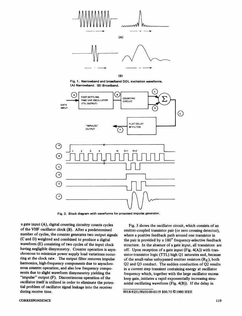
Generation of the linear FM transmit pulse in modemchirp radars is often accomplished by excitation of the re-ceiver dispersive delay line (DDL) with a waveform whosespectral envelope is essentially flat over the effective band-width of the DDL [1-31. This is sometimes accomplishedusing a relatively high-level, narrow video pulse. Becauseof the large out-of-band spectral content of this type ofwaveform, its use is relatively inefficient and can resultin undesirable levels of spurious emission in the radartransmit spectrum. A more efficient and therefore morecommonly used excitation waveform is in the form ofa gated sinusoid, as shown in Fig. 1. For low-resolution(narrow-bandwidth) systems, where the waveform con-tains many cycles of a high-frequency carrier, the wave-form of Fig. 1(A) is typically generated using a simplegated oscillator. Unfortunately, this type of circuit me-chanization is not suitable for use in high-resolution, large,percentage-bandwidth systems (Fig. 1(B)), where therequired DDL excitation "impulse" waveform containstypically two or three cycles of a VHF carrier and where"instant" oscillator turn-on would be required.
Because of the inadequacies of the gated oscillatorcircuit, several alternative schemes for generation of theVHF impulse were considered. The most obvious methodconsidered was generation of a VHF carrier followed bya very fast diode RF switch. This mechanization hasseveral drawbacks, including uncontrolled starting phase,switch video (gating signal) transient leakage, required fastswitching times, and the problem of switch on and offstate voltage standing-wave ratio (VSWR) variations. Asan alternative to this type of mechanization, the authorshave utilized a simple, reliable, and extremely flexiblemeans for generation of the required DDL excitationwaveform.
Circuit Description
Fig. 2 indicates, in conceptual form, the new means
for generating the required DDL impulse excitation signal.The circuitry contains three functional subcircuits: a
fast amplitude settling time VHF oscillator, a digital count-ing circuit, and a low-phase-distortion output bandpassfilter. The waveforms indicate device operation. Following
Manuscript received April 4,1979; revised August 31, 1979.
IEEE TRANSACTIONS ON AEROSPACE AND ELECTRONIC SYSTEMS VOL. AES-16, NO. 1 JANUARY 1980118
\t
(A)
(B)
Fig. 1. Narrowband and broadband DDL excitation waveforms.(A) Narrowband. (B) Broadband.
GATEINPUT
0D
1 2 3 4 N N+1 N+2
Fig. 2. Block diagram with waveforms for proposed impulse generator.
a gate input (A), digital counting circuitry counts cyclesof the VHF oscillator clock (B). After a predeterminednumber of cycles, the counter generates two output signals(C and D) weighted and combined to produce a digitalwaveform (E) consisting of two cycles of the input clockhaving negligible dissymmetry. Counter operation is asyn-
chronous to minimize power supply load variations occur-
ring at the clock rate. The output filter removes impulseharmonics, high-frequency components due to asynchro-nous counter operation, and also low frequency compo-
nents due to slight waveform dissymmetry yielding the"impulse" output (F). Discontinuous operation of theoscillator itself is utilized in order to eliminate the poten-tial problem of oscillator signal leakage into the receiverduring receive time.
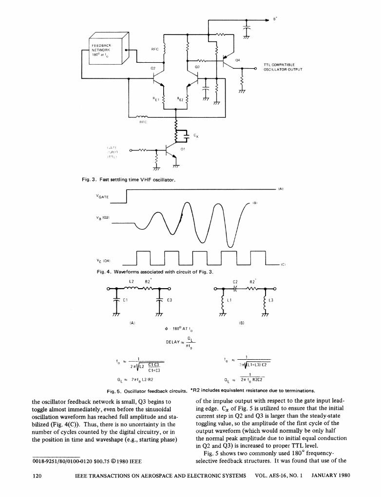
Fig. 3 shows the oscillator circuit, which consists of anemitter-coupled transistor pair (or zero crossing detector),where a positive feedback path around one transistor inthe pair is provided by a 1800 frequency-selective feedbackstructure. In the absence of a gate input, all transistors areoff. Upon reception of a gate input (Fig. 4(A)) with tran-sistor-transistor logic (TTL) high Ql saturates and, becauseof the small-value unbypassed emitter resistors (RE), bothQ2 and Q3 conduct. The sudden conduction of Q2 resultsin a current step transient containing energy at oscillatorfrequency which, together with the large oscillator excessloop gain, initiates a rapid exponentially increasing sinu-soidal oscillating waveform (Fig. 4(B)). If the delay in
0018-9251/80/0100-0119 $00.75 i) 1980 IEEE
CORRESPONDENCE
A
Ch(3
(D
0D I
119
B4
Fig. 3. Fast settling time VHF oscillator.
VGATE
TTL COMPATIBLEOSCiLLATOR OUTPUT
- ~(A)
(B)
vB (02)
VFC (04)
(C0
Fig. 4. Waveforms associated with circuit of Fig. 3.
L2 R2
(A)0 1800 AT to
QLDELAY ;-ITf0
2 orL2 Cl C3
Q L ho2nto L2/R2
C2 R2
L1 L3
(B)
t I
0.r)Fl+L3) C2
1
aL;z 21tor R2C
Fig. 5. Oscillator feedback circuits. *R2 includes equivalent resistance due to terminations.
the oscillator feedback network is small, Q3 begins totoggle almost immediately, even before the sinusoidaloscillation waveform has reached full amplitude and sta-bilized (Fig. 4(C)). Thus, there is no uncertainty in thenumber of cycles counted by the digital circuitry, or inthe position in time and waveshape (e.g., starting phase)
0018-9251/80/0100-0120 $00.75 © 1980 IEEE
of the impulse output with respect to the gate input lead-ing edge. Cx of Fig. 5 is utilized to ensure that the initialcurrent step in Q2 and Q3 is larger than the steady-statetoggling value, so the amplitude of the first cycle of theoutput waveform (which would normally be only halfthe normal peak amplitude due to initial equal conductionin Q2 and Q3) is increased to proper TTL level.
Fig. 5 shows two commonly used 1800 frequency-selective feedback structures. It was found that use of the
IEEE TRANSACTIONS ON AEROSPACE AND ELECTRONIC SYSTEMS VOL. AES-16, NO. 1 JANUARY 1980120
> +15 Vdc
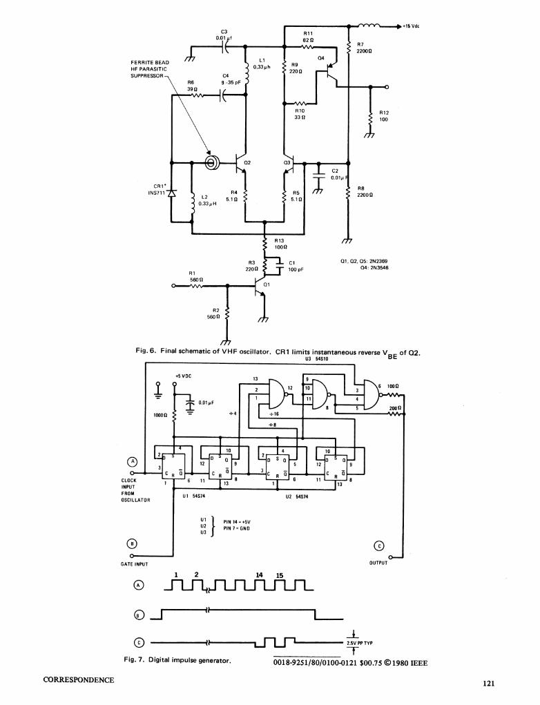
reverse VBE of Q2.
1 2 14 15
(D
oE LFU Iy(gD i ugeo0 /'I 2.5VPP TYP
Fig. 7. Digital impulse generator. 0018-9251/80/0100-0121 $00.75 C)1980 IEEE
CORRESPONDENCE 121
Fig. 6.
GATE INPUT
LI C150S2 0.18jH 280 pF C2L2
V3 ~~~~~ ~ ~ ~ ~ p9:~~~~~~~~~0.53FtH50
Vg Q ~~~~~ ~~ ~~~~C 1231 pF5S
v 7 t67pFa
(A)C1
280 pF
0-I-~
C231 pf
C12
CB23 pF
CA 5.5 pF50pF cc
CoN
(B)
N2L1 = 0.39pH L2 - 0.56jH
RL = 50s
(C)N =
54510
10 . (TYP)
t 1.48 =50 Ri
1500
0.39uH 0.56 pH
(12 pF ACTUAL)
V2 RS I1 0in
(D)
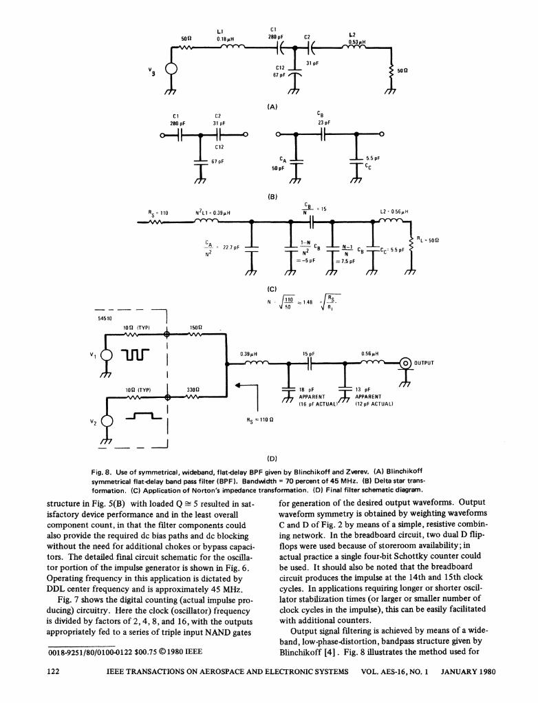
Fig. 8. Use of symmetrical, wideband, flat-delay BPF given by Blinchikoff and Zverev. (A) Blinchikoff
symmetrical flat-delay band pass filter (BPF). Bandwidth = 70 percent of 45 MHz. (B) Delta star trans-
formation. (C) Application of Norton's impedance transformation. (D) Final filter schematic diagram.
structure in Fig. 5(B) with loaded Q 5 resulted in sat-
isfactory device performance and in the least overallcomponent count, in that the filter components couldalso provide the required dc bias paths and dc blockingwithout the need for additional chokes or bypass capaci-tors. The detailed final circuit schematic for the oscilla-
tor portion of the impulse generator is shown in Fig. 6.Operating frequency in this application is dictated byDDL center frequency and is approximately 45 MHz.
Fig. 7 shows the digital counting (actual impulse pro-
ducing) circuitry. Here the clock (oscillator) frequencyis divided by factors of 2, 4, 8, and 16, with the outputs
appropriately fed to a series of triple input NAND gates
0018-9251180/0100-0122 $00.75 i 1980 IEEE
for generation of the desired output waveforms. Outputwaveform symmetry is obtained by weighting waveformsC and D of Fig. 2 by means of a simple, resistive combin-
ing network. In the breadboard circuit, two dual D flip-flops were used because of storeroom availability; in
actual practice a single four-bit Schottky counter could
be used. It should also be noted that the breadboardcircuit produces the impulse at the 14th and 15th clock
cycles. In applications requiring longer or shorter oscil-lator stabilization times (or larger or smaller number of
clock cycles in the impulse), this can be easily facilitated
with additional counters.Output signal filtering is achieved by means of a wide-
band, low-phase-distortion, bandpass structure given byBlinchikoff [4]. Fig. 8 illustrates the method used for
IEEE TRANSACTIONS ON AEROSPACE AND ELECTRONIC SYSTEMS VOL. AES-16, NO. 1 JANUARY 1980
RS 110
V1
122
adaption of the Blinchikoff filter for the case of unequal,matched terminations [5]. The low value of SchottkyNAND gate output impedance in both logic states, com-pared to that of the gate output resistive combining net-work, ensures nearly constant filter source impedance.
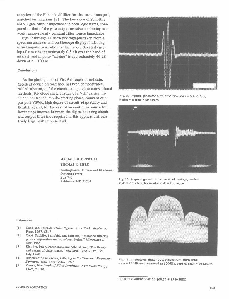
Figs. 9 through 11 show photographs taken from aspectrum analyzer and oscilloscope display, indicatingactual impulse generation performance. Spectral enve-lope flatness is approximately 0.5 dB over the band ofinterest, and impulse "ringing" is approximately 46 dBdown at t - 100 ns.
Conclusions
As the photographs of Fig. 9 through 11 indicate,excellent device performance has been demonstrated.Added advantage of the circuit, compared to conventionalmethods (RF diode switch gating of a VHF carrier) in-clude: controlled impulse starting phase, constant out-put port VSWR, high degree of circuit adaptability andflexibility, and, for the case of an emitter or source fol-lower stage inserted between the digital counting circuitand output filter (not required in this application), rela-tively large peak impulse level.
MICHAEL M. DRISCOLL
THOMAS K. LISLE
Westinghouse Defense and ElectronicSystems CenterBox 746Baltimore, MD 21203
References
[11 Cook and Bernfeld, Radar Signals. New York: AcademicPress, 1967, Ch. 3.
[2] Cook, Paolillo, Bernfeld, and Palmieri, "Matched filteringpulse compression and waveform design," Microwave J.,Nov. 1964.
[3] Klauder, Price, Darlington, and Albersheim, "The theoryand design of chirp radars," Bell Syst. Tech. J., vol. 39,July 1960.
[4] Blinchikoff and Zverev, Filtering in the Time and FrequencyDomains. New York: Wiley, 1976.
[5] Zverev, Handbook of Filter Synthesis. New York: Wiley,1967, Ch. 10.
Fig. 9. Impulse generator output; vertical scale = 50 mV/cm,horizontal scale = 50 ns/cm.
Fig. 10. Impulse generator output clock leakage; verticalscale = 2 mV/cm, horizontal scale = 100 ns/cm.
Fig. 11. Impulse generator output spectrum; horizontalscale = 10 MHz/cm, centered at 50 MHz, vertical scale = 10 dB/cm.
0018-9251/80/0100-0123 $00.75 ©)1980 IEEE
CORRESPONDENCE 123