quantum transport beyond the effective mass approximation
TRANSCRIPT

Quantum Transport Beyond the Effective Mass Ap-proximation


Diss. ETH No. 17016
Quantum Transport Beyondthe Effective MassApproximation
A dissertation submitted to the
SWISS FEDERAL INSTITUTE OF TECHNOLOGYZURICH
for the degree of
Doctor of Sciences
presented by
MATHIEU LUISIER
Dipl.-Ing. ETHborn 19 12 1978
citizen of Switzerland
accepted on the recommendation of
Prof. Dr. Wolfgang Fichtner, examinerProf. Dr. Mark Lundstrom, co-examiner
2007

Acknowledgments
During almost four years I had the pleasure to work at the IntegratedSystems Laboratory under the direction of Prof. Wolfgang Fichtner.I would like to thank him for this opportunity and for the freedomhe gave me in my research work. I am also grateful to Prof. MarkLundstrom for accepting to be the co-examiner of this thesis and forhosting me during six months, together with Prof. Gerhard Klimeck,at the Network for Computational Nanotechnology (NCN), PurdueUniversity. I wish to thank Prof. Andreas Schenk, too, for readingand correcting my report on quantum transport and this thesis.
The various discussions I had with the members of the TCADgroup and of the Computational Optoelectronics group were benefi-cial for this work. Special thanks go to Dr. Simon Brugger for the ani-mated debates we had about transport theory and to Dr. Stefan Oder-matt for the time we spent trying to understand the laser gain andthe bandstructure modeling, but also to Ratko Veprek, Martin Frey,Aniello Esposito, Dr. Valerio Laino, Dr. Christoph Muller, Dr. StefanRollin, Dr. Beat Sahli, and Prof. Bernd Witzigmann. I also addressmy sincere thanks to the members (or ex-members) of the NCN and toProf. Eric Polizzi (University of Amherst) and Prof. Timothy Boykin(University of Alabama) for their useful advise.
Thanks to Dr. Dolf Aemmer, Christoph Wicki, Anja Bohm, andChristine Haller, the working conditions at the institute were optimal,letting me concentrate on research only.
Finally I express my deep gratitude to my parents, Rene and Anne,who always supported me during my studies, in the good and in thebad moments. Without their encouragement I would never have cometo the ETHZ.
v

vi ACKNOWLEDGMENTS
This work was partially funded by the Swiss National Fond, ProjectNo. 200021-109393 (NEQUATTRO).

Abstract
A three-dimensional full band simulator for nanowire field-effect tran-sistors (FETs) is presented in this thesis. At the nanometer scale theclassical drift-diffusion transport theory reaches its limits; quantumtransport (QT) phenomena govern the motion of electrons and holes.The development of a QT simulator requires the assembly of severalphysical models and the choice of appropriate simplifications.
In the first part, the Non-Equilibrium Green’s Function (NEGF)formalism is reviewed, a method extensively used for the descriptionof nanostructures. It is applied to the simulation of a two-dimensionalultra-thin-body (UTB) transistor and of a three-dimensional nanowireFET, both treated within the effective mass approximation (EMA)and in a coupled mode-space. However, the strong quantization effectsthat characterize structures with dimensions below five nanometersoblige an accurate QT simulator to go beyond the EMA.
The semi-empirical sp3d5s∗ tight-binding (TB) method is chosenas bandstructure model because (1) it reproduces the complete bulk(E−k) relation of a wide range of semiconductor materials, (2) it usesan atomic grid, and (3) its extension to nanostructures is straightfor-ward. The integration of the TB method into a transport code is onlypossible, if open boundary conditions (OBC) are introduced. Theavailable procedures to apply OBC in a three-dimensional multibandQT simulator are computationally too intensive since they represent ageneralized eigenvalue problem or require iterative solvers. Therefore,a new method based on the scattering-boundary approach is devel-oped in this work. It significantly reduces the computational burdenassociated with the OBC calculation. Furthermore, it can be formu-lated either in the NEGF or in the Wave Function formalism, and
vii

viii ABSTRACT
it works for any channel orientation, material composition, and crosssection shape.
Finally, simulations of nanowire FETs are achieved by self-consis-tently coupling the full-band transport solver to the three-dimensionalcomputation of the electrostatic potential in the device (Poisson’sequation). Two different wire types are studied, one with a perfectstoichiometric structure (atoms occupy all the lattice positions) andanother with atomic roughness at the semiconductor-oxide interface.Channel orientations along the [100], [110], [111], and [112] axis areconsidered.

Zusammenfassung
In der vorliegenden Dissertation wird ein Simulator fur dreidimen-sionale Nanowire-Feldeffekt-Transistoren (NW-FETs) prasentiert, dervollstandige Bandstrukturen benutzt. Im Langenbereich von wenigenNanometern stosst die klassische Drift-Diffusions-Transporttheorie anihre Grenzen. Die Bewegung der Ladungstrager wird wesentlich durchQuantenphanomene bestimmt, so dass eine Beschreibung mittelsQuanten-Transport (QT) notwendig wird. Die Entwicklung einesQT-Simulators erfordert die Kombination von verschiedenen physi-kalischen Modellen und die Wahl geeigneter Vereinfachungen.
Zuerst wird die Methode der Greenschen Funktionen im Nicht-gleichgewicht (Non-Equilibrium Green’s Functions - NEGF) wieder-holend dargestellt, die fur ihre breite Anwendung auf Nanostrukturenbekannt ist. Sie wird dann fur die Simulation eines zweidimensio-nalen Ultra-Thin-Body-Transistors und eines dreidimensionalen NW-FETs eingesetzt. Beide Bauelemente werden mittels Effektivmassen-Approximation (EMA) in einem gekoppelten Modenraum behandelt.In Strukturen mit Abmessungen von weniger als funf Nanometernwerden die Quanteneffekte jedoch so stark, dass ein leistungsfahigerQT-Simulator uber die EMA hinausgehen muss.
Als Bandstruktur-Modell wird die semi-empirische sp3d5s∗ Tight-Binding-Methode (TB-Methode) gewahlt, da sie (i) die vollstandigeE − k-Relation von verschiedenen Volumen-Halbleitern reproduziert,(ii) ein Atomgitter verwendet, und (iii) weil ihre Ausdehnung aufNanostrukturen unkompliziert ist. Die Integration von TB-Band-strukturen in einem QT-Simulator gelingt nur, wenn offene Rand-bedingungen (Open Boundary Conditions - OBC) gestellt werden.Bestehende Verfahren, mit denen die OBC in einem dreidimensiona-
ix

x ZUSAMMENFASSUNG
len Multiband-QT-Simulator behandelt werden konnen, sind jedochzu zeitaufwendig (iterative Loser und verallgemeinerte Eigenwertpro-bleme). Daher wird in der vorliegenden Arbeit eine neue Methodeentwickelt, die auf der Scattering-Boundary-Naherung basiert. Mitdieser Methode wird der Rechenaufwand, der aus den OBC entsteht,entscheidend verringert. Sie kann sowohl im Rahmen der NEGF, alsauch in einer Theorie basierend auf Wellenfunktionen, formuliert wer-den und funktioniert fur jede Kanal-Orientierung, fur beliebige Mate-rialien und fur alle Querschnittsformen.
Im letzten Teil der Arbeit werden selbstkonsistente Simulationenvon NW-FETs durchgefuhrt, indem das Multiband-Transportmodellmit der Berechnung des dreidimensionalen elektrostatischen Bauele-mentpotentials (Poisson Gleichung) gekoppelt wird. Zwei verschie-dene Typen von NW-FETs werden untersucht: (i) mit perfekter sto-chiometrischer Struktur (Atome besetzen alle Gitterstellen des geome-trisch idealen Quantendrahts) und (ii) mit einer Oberflachen-Rauhig-keit auf atomarer Skala an der Halbleiter-Oxid-Grenzflache. Es wer-den Kanal-Orientierungen entlang [100], [110], [111] und [112] betrach-tet.

Contents
Acknowledgments v
Abstract vii
Zusammenfassung ix
1 Introduction 1
2 Non-Equilibrium Green’s Function 52.1 Introduction . . . . . . . . . . . . . . . . . . . . . . . . 52.2 Definition . . . . . . . . . . . . . . . . . . . . . . . . . 62.3 Langreth Theorem . . . . . . . . . . . . . . . . . . . . 92.4 Basis Expansion . . . . . . . . . . . . . . . . . . . . . 122.5 Tight-Binding Approximation . . . . . . . . . . . . . . 142.6 Stationary Solution . . . . . . . . . . . . . . . . . . . . 152.7 Closed Set Of Equations . . . . . . . . . . . . . . . . . 162.8 Self-Energy Examples . . . . . . . . . . . . . . . . . . 17
2.8.1 Carrier-Carrier Interaction . . . . . . . . . . . 172.8.2 Carrier-Phonon Interaction . . . . . . . . . . . 182.8.3 Impurity Scattering . . . . . . . . . . . . . . . 19
2.9 Boundary Conditions . . . . . . . . . . . . . . . . . . . 192.10 Carrier and Current Densities . . . . . . . . . . . . . . 222.11 Summary . . . . . . . . . . . . . . . . . . . . . . . . . 23
3 Effective Mass Approximation 253.1 Introduction . . . . . . . . . . . . . . . . . . . . . . . . 25
xi
xii CONTENTS
3.2 Theory . . . . . . . . . . . . . . . . . . . . . . . . . . . 263.2.1 Real-Space Approach . . . . . . . . . . . . . . 283.2.2 Coupled Mode-Space approach . . . . . . . . . 30
3.3 Applications . . . . . . . . . . . . . . . . . . . . . . . . 343.3.1 Two-dimensional device: Si UTB . . . . . . . . 353.3.2 Three-dimensional device: Si Nanowire . . . . . 40
3.4 Discussion . . . . . . . . . . . . . . . . . . . . . . . . . 463.5 Summary . . . . . . . . . . . . . . . . . . . . . . . . . 47
4 Bandstructure Model 494.1 Introduction . . . . . . . . . . . . . . . . . . . . . . . . 494.2 Theory . . . . . . . . . . . . . . . . . . . . . . . . . . . 50
4.2.1 Bulk . . . . . . . . . . . . . . . . . . . . . . . . 504.2.2 Nanostructures . . . . . . . . . . . . . . . . . . 534.2.3 Strain . . . . . . . . . . . . . . . . . . . . . . . 58
4.3 Results . . . . . . . . . . . . . . . . . . . . . . . . . . . 594.4 Summary . . . . . . . . . . . . . . . . . . . . . . . . . 64
5 Transport Model 655.1 Introduction . . . . . . . . . . . . . . . . . . . . . . . . 655.2 Theory . . . . . . . . . . . . . . . . . . . . . . . . . . . 67
5.2.1 Wave Function Solver . . . . . . . . . . . . . . 745.2.2 NEGF Solver . . . . . . . . . . . . . . . . . . . 765.2.3 Quantum Well Reservoir . . . . . . . . . . . . . 78
5.3 Results . . . . . . . . . . . . . . . . . . . . . . . . . . . 815.3.1 Ideal Contacts . . . . . . . . . . . . . . . . . . 815.3.2 Quantum Well and Mixed Contacts . . . . . . 965.3.3 Alloy Disorder . . . . . . . . . . . . . . . . . . 96
5.4 Discussion . . . . . . . . . . . . . . . . . . . . . . . . . 1005.5 Summary . . . . . . . . . . . . . . . . . . . . . . . . . 102
6 Self-Consistent Simulations 1036.1 Introduction . . . . . . . . . . . . . . . . . . . . . . . . 1036.2 Theory . . . . . . . . . . . . . . . . . . . . . . . . . . . 1046.3 Results . . . . . . . . . . . . . . . . . . . . . . . . . . . 1086.4 Summary . . . . . . . . . . . . . . . . . . . . . . . . . 116
7 Conclusion and Outlook 119

CONTENTS xiii
A Interaction Representation 121A.1 Schrodinger Picture . . . . . . . . . . . . . . . . . . . 121A.2 Heisenberg Picture . . . . . . . . . . . . . . . . . . . . 122A.3 Interaction Picture . . . . . . . . . . . . . . . . . . . . 122A.4 Expectation Values . . . . . . . . . . . . . . . . . . . . 124
B EM Hamiltonian 127
C From NEGF to Wave Function 129
Curriculum Vitae 141


Chapter 1
Introduction
Nowadays microprocessors build the core of most of the electronic in-struments, from personal computers to mobile phones, DVD players,car brake systems, and so on. The constant request for performanceimprovement is mainly satisfied in three different ways. First, an in-crease of the microprocessor surface offers the possibility of integratingmore functionality on the same board. Secondly, circuit designers andsoftware engineers optimize the available resources. Thirdly, the sizeof the transistors constituting the active part of the microprocessorsis decreased.
Practical limits of the chip area force the semiconductor indus-try to put a lot of its efforts on transistor miniaturization. Thirtyyears of aggressive scaling have pushed the device dimensions closeto the atomic range. Recently reported structures of metal-oxide-semiconductor field-effect transistors (MOSFETs) already have chan-nel lengths in the order of 10 nm or even smaller[1]. Such shortchannels are hard to fabricate, induce source-to-drain tunneling, andrequire very thin oxide layers causing significant gate leakage cur-rents. The search for advanced device architectures that could over-come these difficulties has just started. It is part of the new researchfield called nanoelectronics.
Semiconductor nanowires (NWs) may play an important role inthe future of nanoelectronics, since they can act both as active de-vices (transistors) and as wire connectors. Recently, several groups
1

2 CHAPTER 1. INTRODUCTION
have grown Si[2], GaAs[3], or Ge[4] NWs with different channel ori-entations and cross section shapes. Field-effect transistors (FETs)with a triangular[5], rectangular[6], or cylindrical[7] wire as channelhave been reported in the literature. Nanostructures with even moreexotic cross sections, such as T-shape wires, have found practical ap-plications, for example in the optoelectronics area[8].
The fabrication of novel devices is a long and expensive process.A well-established way of accelerating the production and of reducingthe costs consists in replacing experimental development techniquesby technology computer aided design (TCAD). In this work, simula-tion tools based on state-of-the-art semiconductor physics have beendeveloped for studying and designing future post-CMOS transistors,with emphasize on nanowire FETs. To properly describe and modelthe current flow in these nanodevices, it becomes necessary to abandonclassical concepts and to include quantum mechanical phenomena[9].With appropriate simplifications to manage the computational bur-den, the Non-Equilibrium Green’s Function (NEGF) formalism[10, 11]and the Wave Function formalism[12] provide a suitable frameworkfor simulating quantum transport in nanowire-based devices. Never-theless, the large amount of grid points necessary to describe thesethree-dimensional structures asks for large computational resources.
A reduction of the nanowires cross sections should ease the simu-lation, as the number of grid points is lowered. However, this ignoresthe fact that electronic transport in nanowires with a size comparableto the de Broglie wavelength exhibits significant quantization effects.Thus the inclusion of the full crystal bandstructure is essential fordevices with a cross section smaller than 5 nm × 5 nm[13]. A cor-rect behavior in the vicinity of the conduction and the valence bandedges (effective mass approximation) is not sufficient. The result is adescription of each grid point by a matrix, instead of a scalar, whosesize reflects the complexity of the bandstructure model. Nanoscale di-mensions do not relax the computational burden, but, on the contrary,they increase it.
An additional challenge is related to the treatment of scatteringeffects, particularly carrier-phonon interactions, that generate fur-ther computational efforts. At this stage, it does not seem possi-ble, within a reasonable time, to simulate realistic three-dimensionalnanostructures with the simultaneous inclusion of full-band and scat-

3
tering effects. However, the influence of both effects has been al-ready treated separately on a one-dimensional example, the resonant-tunneling diode (RTD)[14]. Important features of this device are theposition and the magnitude of its valley current. The authors ofRef. [14] found that the correct reproduction of these characteristicsdepends more on the accuracy of the bandstructure model than onthe inclusion of the electron-phonon interactions.
Therefore, the efforts are focused on the bandstructure effects insemiconductor nanowires and quantum transport beyond the effectivemass approximation is considered. Results are presented in Chapter6 of this thesis. The development of a three-dimensional, full-band,quantum transport simulator requires several steps. In Chapter 2,the NEGF formalism is reviewed, from the two-time definition of theGreen’s function to its practical form for simulations. It is shownhow the boundary conditions are included, how to express the Green’sfunction in different basis representations, and how to calculate carrierand current densities.
Chapter 3 is dedicated to the effective mass approximation (EMA).Although it does not allow a correct description of the quantizationeffects in nanostructures, it can be used as a reference to estimatethe importance of a full bandstructure. A simplification scheme, thecoupled mode-space, is applied to the EMA-NEGF formalism andserves as basis for the simulation of a two-dimensional ultra-thin body(UTB) MOSFET and a three-dimensional nanowire FET.
Since the EMA fails when the confinement of the carriers becomesimportant, it is necessary to find a more appropriate bandstructuremodel. In Chapter 4 it is shown why the sp3d5s∗ semi-empirical tight-binding model is the method of choice . Its capability of reproducingthe full bandstructure of diamond (Si), zincblende (GaAs), wurtzite(GaN), and other crystal structures, as well as its atomic descriptionof the simulation domain are both determining arguments.
In Chapter 5 the sp3d5s∗ tight-binding method is coupled to ananowire quantum transport solver. The calculation of the openboundary conditions (OBC) is improved to reduce the computationalburden. It is demonstrated how the OBC can be integrated into aNEGF or Wave Function solution scheme. The main achievementsare the simulation of nanowires with different cross sections and chan-nel orientations, the inclusion of mechanical strain, the possibility of

4 CHAPTER 1. INTRODUCTION
treating non-ideal contacts, and the investigation of alloy disorder.Finally, Chapter 6 assembles the models from the previous chap-
ters and presents the simulation of Si nanowires with different channelorientations. The three-dimensional electrostatic potential is com-puted self-consistently with the device charge density. The full-bandcurrent characteristics are compared to the EMA results. Althoughscattering effects are out of the scope of this work, the tight-bindingformalism is well-suited for the simulation of nanowires with semi-conductor-oxide interface roughness.
The TCAD tools developed in this work comprise a two- and athree-dimensional coupled mode-space/real-space EMA-NEGF solver,a bulk, UTB, nanowire bandstructure calculator, and a parallel, three-dimensional, full-band nanowire simulator.
Chapter 2
Non-EquilibriumGreen’s Function
2.1 Introduction
The concept and the first applications of the non-equilibrium Green’sfunction (NEGF) were given by Schwinger[15], Kadanoff and Baym[16],Fujita[17], and Keldysh[18] at the beginning of the 1960’s.
The NEGF formalism provides a conceptual basis for the develop-ment of quantum-mechanical simulators needed to design post-CMOSnanoscale devices. It works with the effective mass approximation[19],but it allows the inclusion of sophisticated bandstructure models onan atomic level[14]. Any kind of scattering can be treated, using thesimplest[11, 20] or the most advanced approximation[21, 22], but bal-listic transport remains the most widespread form[23, 24, 25, 26].
In this Chapter, the NEGF formalism is reviewed, discussing itsdefinition in the time domain, its equation of motion, its basis expan-sion, its stationary solution in the energy domain, the inclusion of abandstructure model and of scattering, the open boundary conditions,and, finally, the calculation of observable variables such as carrier andcurrent densities. The relation to the Wave Function formalism isderived in Appendix C.
5

6 CHAPTER 2. NON-EQUILIBRIUM GREEN’S FUNCTION
2.2 Definition
According to the expectation value of operators expressed in theHeisenberg picture (see Appendix A), the one-particle non-equilibriumGreen’s function, labeled G(r, t; r′, t′) is defined as
G(r, t; r′, t′) = − i�〈T{ψH(r, t)ψ†
H(r′, t′)}〉
= − i�(θ(t, t′)〈ψH(r, t)ψ†
H(r′, t′)〉 −
θ(t′, t)〈ψ†H(r′, t′)ψH(r, t)〉). (2.1)
The operator ψ†H(r′, t′) (ψH(r, t)) creates (annihilates) a particle at
position r′ (r) and time t′ (t). The time-ordering operator T ordersthe operators along the contour C in Fig. A.1. The function θ(t, t′)is defined on the same contour C with θ(t, t′) = 1, if t is later on Cthan t′, or in a mathematical expression
t > t′ t′ > tt later on C θ(t− t′) θ(t′ − t)t′ later on C θ(t′ − t) θ(t− t′)
(2.2)
and its time-derivative is given by
ddtθ(t, t′) = δ(t, t′) = − d
dtθ(t′, t). (2.3)
The δ-function δ(t, t′) is defined on a contour with the same propertiesas Eq. (2.2), but with additional negative signs in the non-diagonalblocks.
The non-equilibrium Green’s function G(r, t; r′, t′) expresses a cor-relation between two times t and t′ and two positions r and r′. For tlater on C than t′, G(r, t; r′, t′) describes the reaction of a system to aparticle created at position r′ and time t′, to the propagation of thisperturbation to position r and time t, and finally to its annihilationthere. A similar interpretation can be found if t′ is later on C than t.
To calculate the time evolution of G(r, t; r′, t′), its equations ofmotion is derived in the Heisenberg picture with respect to time t andto time t′. For that purpose, the Hamilton operator H = H0 + V
2.2. DEFINITION 7
is introduced. H0 contains the lattice and the electrostatic potential,while V includes the scattering mechanisms. For brevity, only carrier-carrier interactions are considered here, but it is shown later in thisChapter how to treat other phenomena. In the notation of secondquantization, the Hamiltonian reads
H = H0 + V
=∫
dr ψ†(r)H0(r)ψ(r)
+12
∫dr∫
dr′ ψ†(r)ψ†(r′)V (r− r′)ψ(r′)ψ(r). (2.4)
To derive the NEGF equations of motion, dG(r, t; r′, t′)/dt, as well asdG(r, t; r′, t′)dt′, some useful abbreviations are required: 1 = (r1, t1),V (1 − 2) = V (r1 − r2)δ(t1 − t2), δ(12) = δ(t1, t2)δ(r1 − r2), and∫C
d1 =∫C
dt1∫
dr1. The time integration is in the complex plane,along the contour C in Fig. A.1. For the derivative with respect to tone obtains
ddtT{ψH(r, t)ψ†
H(r′, t′)}
= T
{ddtψH(r, t)ψ†
H(r′, t′)}
+
δ(t, t′)[ψH(r, t), ψ†
H(r′, t)]+
= T
{ddtψH(r, t)ψ†
H(r′, t′)}
+
δ(t, t′)δ(r− r′), (2.5)
where the second term of the right-hand side (δ(t, t′)δ(r− r′)) resultsfrom the time derivative of the time-ordering operator T . It also takesinto account the commutation property of the creation and annihila-tion operators [
ψH(r, t), ψ†H(r′, t)
]+
= δ(r− r′). (2.6)
To evaluate the first right-hand side term in Eq. (2.5), it is neces-sary to know the time evolution of the annihilation operator ψH(r, t).Since it is expressed in the Heisenberg picture, the equation of motion

8 CHAPTER 2. NON-EQUILIBRIUM GREEN’S FUNCTION
(A.7) can be applied after the Hamiltonian H in Eq. (2.4) has beentransformed into this basis
i�ddtψH(r, t) =
[ψH(r, t), HH(t)
]= H0(r)ψH(r, t) + (2.7)∫
dr′ V (r− r′)ψ†H(r′, t)ψH(r′, t)ψH(r, t).
Multiplying Eq. (2.7) by the creation operator ψ†H(r′, t), adding the
second right-hand side term of Eq. (2.5), applying the time-orderingoperator T , and building the expectation value of the overall expres-sion gives the equation of motion of the non-equilibrium Green’s func-tion G(r, t; r′, t′).
By taking into account the above considerations, the equation ofmotion for G(r, t; r′, t′) = G(11′) relative to t becomes(
i�ddt
−H0(r))G(11′) = δ(11′) − (2.8)
i�
∫C
d3 V (1 − 3) G(2)(13−1′3+)
and relative to t′(−i� d
dt′−H0(r′)
)G(11′) = δ(11′) − (2.9)
i�
∫C
d3 V (1′ − 3) G(2)(13−1′3+)
where the two-particle Green’s function G(2)(131′3′) is defined as
G(2)(131′3′) =(− i
�
)2
〈T{ψH(1)ψH(3)ψ†
H(3′)ψ†H(1′)
}〉. (2.10)
Equations (2.8) and (2.9) induce an infinite hierarchy, because thetime evolution of the one-particle Green’s function G(11′) requiresthe knowledge of the two-particle Green’s function G(2)(131′3′). Inturn, the equation of motion for the two-particle Green’s functioncontains three-particle Green’s functions and so on. To truncate this

2.3. LANGRETH THEOREM 9
infinite hierarchy the self-energy Σ(11′) is introduced in the secondright-hand-side term of Eqs. (2.8) and (2.9)(
i�ddt
−H0(r))G(11′) = δ(11′) +
∫C
d3 Σ(13)G(31′), (2.11)(−i� d
dt′−H0(r′)
)G(11′) = δ(11′) +
∫C
d3 G(13)Σ(31′). (2.12)
Equations (2.11) and (2.12) are the result of the application of Feyn-man diagrams[27], Wick’s decomposition[28], or functional derivatives[29] to approximate the two-particle Green’s function G(2)(131′3′).These techniques allow different orders of complexity, from the Har-tree-Fock[30] to the Second Born approximation[22], without any up-per limit. Some examples will be given later in this Chapter.
2.3 Langreth Theorem
The equations of motion for the non-equilibrium Green’s functionG(11′) include integrals over a complex time-loop
∫C
. They are ratherimpractical in calculations unless they are replaced by real time in-tegrals. Since it is not obvious to keep track of time-branch in theevaluation of
∫C
in Fig. A.1, four new Green’s functions with realtime arguments are defined
G(11′) =
Gc(11′) t,t′ on Cc,Ga(11′) t, t′ on Ca,G<(11′) t on Cc, t′ on Ca,G>(11′) t on Ca, t′ on Cc.
(2.13)
Here, Cc (Ca) represents the chronological (anti-chronological) part ofthe contour C in Fig. A.1. The chronologically time-ordered Green’sfunction Gc(11′) (with T c from Eq. (A.16))
Gc(11′) = − i�〈T c{ψH(1)ψ†
H(1′)}〉, (2.14)
the anti-chronologically time-ordered Green’s function Ga(11′) (withT a from Eq. (A.19))
Ga(11′) = − i�〈T a
{ψH(1)ψ†
H(1′)}〉, (2.15)

10 CHAPTER 2. NON-EQUILIBRIUM GREEN’S FUNCTION
the lesser Green’s function G<(11′)
G<(11′) =i
�〈ψ†
H(1′)ψH(1)〉, (2.16)
and the greater Green’s function G>(11′)
G>(11′) = − i�〈ψH(1)ψ†
H(1′)〉 (2.17)
are not linearly independent functions because Gc +Ga = G> +G<.For quantum transport problems, the most suitable functions areG<(11′) and G>(11′) that are directly related to observables. Theadvanced GA(11′) and the retarded GR(11′) Green’s functions arepreferred to the unusual Ga(11′) and Gc(11′)
GA(11′) = Gc(11′) −G>(11′), (2.18)GR(11′) = Gc(11′) −G<(11′), (2.19)
with GR − GA = G> − G<. The same conventions are applied toΣ(11′) leading to the lesser Σ<(11′), the greater Σ>(11′), the advancedΣA(11′) and the retarded ΣR(11′) self-energies. The relation ΣR −ΣA = Σ> − Σ< holds in this case, too[30].
In the equations of motion (2.11) and (2.12), terms of the formC = AB are encountered, or, explicitly,
C(t, t′) =∫C1
dτ A(t, τ)B(τ, t′), (2.20)
where C1 is the contour of Fig. A.1. To evaluate Eq. (2.20), it is firstassumed that t is on the upper part (chronological branch) and t′ onthe lower part (anti-chronological branch) of the time contour so thatC<(tt′) is calculated. By combining Eq. (2.1) and Eq. (2.13), one has
A(t, τ) = θ(t, τ)A>(t, τ) + θ(τ, t)A<(t, τ),B(τ, t′) = θ(τ, t′)B>(τ, t′) + θ(t′, τ)B<(τ, t′). (2.21)
After these forms are inserted into Eq. (2.20), four different prod-ucts A≷B≷ appear. For example, the term A<B< is preceded byθ(τ, t)θ(t′, τ). This means that τ is later on the time contour than t,

2.3. LANGRETH THEOREM 11
but earlier than t′. Furthermore, t′ is later on C1 than t (assumption).This gives∫
C1
dτ θ(τ, t)θ(t′, τ)A<(t, τ)B<(τ, t′) =∫ t′
t
dτ A<(t, τ)B<(τ, t′)
=∫ t′
t0
dτ A<(t, τ)B<(τ, t′)
−∫ t
t0
dτ A<(t, τ)B<(τ, t′).
The same procedure applies to the three other products in Eq. (2.20)leading to the following expression
C<(t, t′) =∫ t
t0
dτ(A>(t, τ) −A<(t, τ)
)B<(τ, t′) −
∫ t′
t0
dτ A<(t, τ)(B>(τ, t′) −B<(τ, t′)
)(2.22)
=∫ ∞
t0
dτ θ(t− τ) (A>(t, τ) −A<(t, τ))B<(τ, t′) −∫ ∞
t0
dτ A<(t, τ)θ(t′ − τ) (B>(τ, t′) −B<(τ, t′))
=∫ ∞
t0
dτ(AR(t, τ)B<(τ, t′) +A<(t, τ)BA(τ, t′)
).
This is the first part of Langreth’s theorem[31], also written as C< =ARB< +A<BA. Analogously one finds
CR(t, t′) =∫ t
t′dτ AR(t, τ)BR(τ, t′). (2.23)
In a compact form, this relation is expressed as CR = ARBR for theretarded configuration and as CA = AABA for the advanced one.
The equations of motion for G(11′) with respect to time t and withreal time arguments become(
i�ddt
−H0(r))GR(11′) = δ(11′) +
∫ ∞
t0
d3 ΣR(13)GR(31′),

12 CHAPTER 2. NON-EQUILIBRIUM GREEN’S FUNCTION
(i�
ddt
−H0(r))GA(11′) = δ(11′) +
∫ ∞
t0
d3 ΣA(13)GA(31′),(i�
ddt
−H0(r))G<(11′) =
∫ ∞
t0
d3(ΣR(13)G<(31′)+
Σ<(13)GA(31′)), (2.24)
and with respect to time t′(−i� d
dt′−H0(r′)
)GR(11′) = δ(11′) +
∫ ∞
t0
d3 GR(13)ΣR(31′),(−i� d
dt′−H0(r′)
)GA(11′) = δ(11′) +
∫ ∞
t0
d3 GA(13)ΣA(31′),(−i� d
dt′−H0(r′)
)G<(11′) =
∫ ∞
t0
d3(GR(13)Σ<(31′)+
G<(13)ΣA(31′)). (2.25)
The equations for the retarded and the advanced Green’s functionscan be solved independently, except if the retarded and the advancedself-energies depend on the lesser or greater Green’s function. In thiscase, the system of equations (2.24) (or (2.25)) is tightly coupled andvery difficult to solve.
2.4 Basis Expansion
The non-equilibrium Green’s function G(11′) depends on the contin-uous space variables r and r′ through the creation and annihilationoperators ψH(r, t) and ψ†
H(r′, t′). These operators can be expandedin a complete set of orthogonal functions ϕn(r) that form a basis.n can be a wave vector index, a state number index, a x−, y−, or z−position index, an orbital type index, or a combination of these pa-rameters. The characteristics of n are related to the device structure(bulk, quantum well, quantum wire, or quantum dot, periodic bound-ary conditions or not) and to the physical models involved in the sim-ulation (bandstructure complexity and scattering). One starts with

2.4. BASIS EXPANSION 13
the definition of the creation and annihilation operators, expressed inthe Heisenberg picture
ψ†H(r, t) =
∑n
c†n(t)ϕ∗n(r), (2.26)
ψH(r, t) =∑n
cn(t)ϕn(r), (2.27)
where c†n(t) and cn(t) creates and annihilates a particle in a state nat time t, respectively. G(11′) has then the following form
G(11′) =∑n,m
ϕn(r) · 〈T {cn(t)c†m(t′)}〉 · ϕ∗
m(r′)
=∑n,m
ϕn(r) ·Gnm(tt′) · ϕ∗m(r′). (2.28)
Using the orthogonality of the expansion functions, the inverse trans-formation is established
Gnm(tt′) =∫
dr∫
dr′ ϕ∗n(r) ·G(11′) · ϕm(r′). (2.29)
The same relations are derived for the self-energies Σ(11′) so thatEqs. (2.11) and (2.12) become
i�ddtGnm(tt′) −
∑l
hnlGlm(tt′) = δnm(tt′) + (2.30)
∑l
∫C
dt1 Σnl(tt1)Glm(t1t′),
−i� ddt′Gnm(tt′) −
∑l
Gnl(tt′)hlm = δnm(tt′) + (2.31)
∑l
∫C
dt1 Gnl(tt1)Σlm(t1t′),
where hnm =∫
dr ϕ∗n(r)H0(r)ϕm(r). The basis expansions of the
retarded, advanced, and lesser Green’s functions take the same formas above, but they are omitted for brevity.

14 CHAPTER 2. NON-EQUILIBRIUM GREEN’S FUNCTION
2.5 Tight-Binding Approximation
Atomic orbital functions φσ(r−Ri) of type σ (cation or anion, single-band, s−, p−, or d− orbital) and located on an atom at vector positionRi are a special basis choice. The φσ(r−Ri)’s are very localized func-tions so that non-zero matrix-elements with their nearest-neighborsonly are assumed[32].
Four different cases with atomic orbitals used as basis function arestudied. For a bulk structure with periodic boundary conditions inthe x−, y−, and z− direction, one obtains ϕn(r) by forming a Blochsum of the atomic orbitals
ϕn(r) → ϕk,σ =1√N
∑Ri
φσ(r−Ri)eik·Ri
Gnm(tt′) → Gσ1σ2(k; tt′) (2.32)
G(11′) →∑
k,σ1σ2
ϕk,σ1(r)Gσ1σ2(k; tt′)ϕ∗k,σ2
(r′),
N being a normalization constant. In the presence of confinement inthe z− direction or if the periodicity along this axis is broken (het-erostructure, applied voltage), the Bloch sum must be modified
ϕn(r) → ϕkt,σ,zi=
1√Nt
∑Rti
φσ(r− {Rti, zi})eikt·Rti
Gnm(tt′) → Gσ1i1;σ2i2(kt; tt′) (2.33)
G(11′) →∑
k,σ1σ2
∑i1i2
ϕkt,σ1,zi1(r)Gσ1i1;σ2i2(kt; tt′)ϕ∗
kt,σ2,zi2(r′).
The vector Rt = (x, y) denotes the transverse position of the atoms.Nt normalizes the basis wave function. Gσ1i1;σ2i2(kt; tt′) is calculatedfor an atomic chain with atoms located at all the zi positions. Wheny and z have finite dimensions, only x remains periodic and the basisfunctions are given by
ϕn(r) → ϕkx,σ,yj ,zk=
1√Nx
∑xi
φσ(r− {xi, yj , zk})eikxxi
Gnm(tt′) → Gσ1j1k1;σ2j2k2(kx; tt′) (2.34)

2.6. STATIONARY SOLUTION 15
G(11′) →∑
kx,σ1σ2
∑j1k1j2k2
ϕkx,σ1,yj1zk1(r)Gσ1j1k1;σ2j2k2(kx; tt
′)
× ϕ∗kx,σ2,yj2zk2
(r′).
Nx is a normalization constant. Gσ1j1k1;σ2j2k2(kx; tt′) takes all the yj
and zk points into account. Finally, for a structure with no periodicity(quantum dot or biased nanowire), the following ansatz is made forϕn(r) and for the expansion of G(11′)
ϕn(r) → ϕσ,xi,yj ,zk= φσ(r− {xi, yj , zk})
Gnm(tt′) → Gσ1i1j1k1;σ2i2j2k2(tt′) (2.35)
G(11′) →∑σ1σ2
∑i1j1k1i2j2k2
ϕσ1,xi1yj1zk1(r)Gσ1i1j1k1;σ2i2j2k2(tt
′)
× ϕ∗σ2,xi2yj2zk2
(r′).
After the basis functions are chosen, the matrix elements hnm arecalculated. The non-interacting Hamiltonian H0(r)
H0(r) =p2
2m0+∑i
V (r−Ri) +HSPIN (r) (2.36)
is used for that purpose. The simplest approach, called single-bandtight-binding model, consists in taking one orbital type only in φσ(r−Ri) (the anion and the cation are lumped into a single orbital). The ef-fective mass Hamiltonian is composed of the single-band tight-bindingmatrix elements of H0(r), see Chapter 3.
In the multi-band case (sp3s∗[33] or sp3d5s∗[34]), the elements hnmare matrices of size tb. The parameter tb is the number of bandsincluded in the model, for example, tb=20(10) in the sp3d5s∗ modelwith(out) spin-orbit coupling. Details follow in Chapters 4 and 5.
2.6 Stationary Solution
Once the stationary solution of a non-equilibrium system is reached,the greater, the lesser, the retarded and the advanced Green’s func-tions G≷,R,A
nm (tt′) do not depend on t and t′, but on the difference t−t′.

16 CHAPTER 2. NON-EQUILIBRIUM GREEN’S FUNCTION
Since t and t′ do not lie on an imaginary time contour anymore, theFourier transform of the Green’s functions with respect to the timedifference t− t′ can be taken
G≷,R,Anm (E) =
∫d(t− t′) eiE(t−t′)/�G≷,R,A
nm (t− t′). (2.37)
The inverse Fourier transform is defined as
G≷,R,Anm (t− t′) =
12π�
∫dE e−iE(t−t′)/�G≷,R,A
nm (E). (2.38)
The stationary self-energies Σ≷,R,A(t− t′) depend on the time differ-ence t− t′, too and they obey, therefore, the same Fourier transformrules as G≷,R,A
nm (t− t′).
2.7 Closed Set Of Equations
To obtain the stationary characteristics of a given device, the energy-dependent Green’s functions G≷,R,A
nm (E) must be calculated. In thisSection the equations that need to be solved are summarized togetherwith some useful relationships between the different types of Green’sfunctions
EGRnm(E) −
∑l
hnlGRlm(E) = δnm +
∑l
ΣRnl(E)GR
lm(E)
EG<nm(E) −
∑l
hnlG<lm(E) =
∑l
ΣRnl(E)G<
lm(E) +
∑l
Σ<nl(E)GA
lm(E)
G<nm(E) =
∑l,v
GRnl(E)Σ<
lv(E)GAvm(E)
GAnm(E) =
[GR
mn(E)]†
GRnm(E) −GA
nm(E) = G>nm(E) −G<
nm(E). (2.39)
The equalities in (2.39) form a coupled system of equations, whereG<
nm(E) and GRnm(E) have to be evaluated. G<,R,A
nm (E) are matri-ces whose size depends on the structure dimensions, but also on thecomplexity of the bandstructure model.
2.8. SELF-ENERGY EXAMPLES 17
It remains to determine the self-energies Σ<nm(E) and ΣR
nm(E)that describe the scattering mechanisms in the device. They directlydepend on G<,R,A
nm (E) and must, therefore, be solved self-consistentlywith them. Iterative procedures are suitable to accomplish this task,but convergence is often difficult to achieve. A remarkable exampleof a working algorithm is given in Ref. [14].
2.8 Self-Energy Examples
In this Section the Hamilton operators and the resulting self-energiesof different scattering mechanisms are given. The Σ(12)’s are obtainedby drawing Feynman diagrams[27], by applying Wick’s decomposition[28], or by using variational derivatives[29]. For brevity, the generalform of the self-energies is shown (two-time dependence on the contourin Fig. A.1, transient, no basis expansion). Σ≷,R,A
nm (E) can be foundafter tedious calculations or directly in the mentioned references.
2.8.1 Carrier-Carrier Interaction
The Hamilton operator for carrier-carrier interaction is defined inEq. (2.4). The presence of electrons only (no holes) is assumed
Hcc =12
∫dr∫
dr′ψ†(r)ψ†(r′)V (r− r′)ψ(r′)ψ(r). (2.40)
This Hamilton operator leads to an infinite hierarchy of self-energies.The first three self-energies are retained, Hartree , Fock, and directcollision[29]. The two last self-energies are lumped in a single expres-sion labeled ΣFdc(12)
ΣHartree(12) = −i�δ(12)∫
d3 V (1 − 3)G(33+) (2.41)
ΣFdc(12) = i�W (21)G(12). (2.42)
The term W (21) represents the screened Coulomb interaction[27, 29].The self-energy ΣHartree(12) is instantaneous (t1 = t2). Therefore, itdoes not appear explicitly in Eqs. (2.11) and (2.12), but it is included

18 CHAPTER 2. NON-EQUILIBRIUM GREEN’S FUNCTION
in the non-interacting Hamiltonian H0(r) that becomes
H0(r) → H0(r) − i�∫
d3 V (1 − 3)G(33+)
→ H0(r) − eφ(r, t). (2.43)
It can be proved that the Hartree self-energy, cast into the potentialφ(r, t), is nothing else than the solution of the Poisson equation withthe negative charge density ρ(r, t) = ie�G<(11+) (see Section 2.10)
φ(r, t) = i�
∫d3r2
e
4πε|r1 − r2|G<(r2t; r2t)
E(r, t) = −grad φ(r, t) =∫
d3r2r1 − r2
4πε|r1 − r2|3 ρ(r2t)
⇒ div E(r, t) = −div grad φ(r, t) =ρ(r, t)ε
. (2.44)
E(r, t) is the electric field in the device.
2.8.2 Carrier-Phonon Interaction
The Hamilton operator describing carrier-phonon scattering has thefollowing form:
Hcph =∫
dr ψ†(r)∑q
eiq·r
|q|(Caq + C∗a†−q
)ψ(r), (2.45)
where aq (a†−q) is the phonon annihilation (creation) operator in astate with quantum number q,
C = i
√e2
V
�ωLO2
(1ε∞
− 1ε0
)and C = i
√�D2
2V ρcs(2.46)
for carrier-optical-phonon (Frohlich coupling constant) and for carrier-acoustic-phonon interaction, respectively. �ωLO is the energy of thelongitudinal optical phonons, ε∞ the high-frequency dielectric con-stant, ε0 the low frequency dielectric constant, V the device volume,D the material deformation potential, ρ its density, and cs the velocityof sound in this material.

2.9. BOUNDARY CONDITIONS 19
Using Wick’s decomposition, the Feynman diagrams or functionalderivatives, the self-energy for carrier-phonon interactions is obtainedas[21, 35]
Σcph(12) = i�|C|2∑q
eiq·(r1−r2)
|q|2 D(q; tt′)G(12), (2.47)
with the non-interacting phonon Green’s function D(q; tt′)[22]
D(q; tt′) = − i�〈T{aq(t)a†q(t′) + a†−q(t)a−q(t′)}〉. (2.48)
Contrary to the carrier-optical-phonon interaction, the carrier-acoustic-phonon interaction can be efficiently simplified due to its low phononenergies[14].
2.8.3 Impurity Scattering
Impurity scattering is an interaction between a moving carrier and anion at fixed position. Its Hamilton operator is given by
His =∑i
∫dr ψ†(r)V (r−Ri)ψ(r), (2.49)
where V (r−Ri) is the Coulomb potential between a carrier at positionr and an impurity at position Ri. If only the second order perturba-tion is kept, the impurity scattering self-energy is defined as[22]
Σis(12) =ρ
V
∑q
V (q)V (−q)eiq(r1−r2)G(12). (2.50)
Here, ρ is the impurity density, V (q) is the Fourier transform of theCoulomb potential V (r) and V is the device volume.
2.9 Boundary Conditions
In quantum transport simulations, devices with finite dimensions in atleast one direction are considered. The other directions are assumedinfinite. For example, a device can be connected to two equilibrated

20 CHAPTER 2. NON-EQUILIBRIUM GREEN’S FUNCTION
contacts that act as a collector and as an emitter on the electric cur-rent (open boundary conditions). To describe the coupling between adevice and semi-infinite contacts, Eq. (2.39) is recalled, first only forGR
nm(E). Obviously, this equation can be written as a matrix equationwith a decomposition into two domains, a central active region withindex C and a lead region with index L. In fact, the lead region canbe degenerated, if there is more than one semi-infinite contact. Thisdoes not change the formalism derivation. If the self-energies thatjoin the active region and the leads (i.e. Σ<,R,A
LC (E) = Σ<,R,ACL (E)) are
neglected, one has[21](E − hCC − ΣR
CC
)GR
CC − hCLGRLC = I (2.51)(
E − hLL − ΣRLL
)GR
LC − hLCGRCC = 0. (2.52)
For notation homogeneity the energy-dependence of the Green’s func-tions and of the self-energies are omitted. I is the identity matrixof the same size as GR
CC . One introduces the lead retarded Green’sfunction gRLL that represents the correlations between the lead pointswhen the lead and the active region are separated (hCL = hLC = 0)(
E − hLL − ΣRLL
)gRLL = I. (2.53)
By inserting Eq. (2.53) into Eqs. (2.51) and (2.52) expression thatcontains GR
CC only is obtained(E − hCC − ΣR
CC − hCLgRLLhLC
)GR
CC = I. (2.54)
The term hCLgRLLhLC can be written as an additional self-energy ΣRB
CC
resulting from the connection of the active region to the lead(E − hCC − ΣR
CC − ΣRBCC
)GR
CC = I (2.55)
The same procedure has to be repeated for the lesser Green’s functionG<
CC . Since is derivation is similar, calculation details are not shown.One has(
E − hCC − ΣRCC − ΣRB
CC
)G<
CC =(Σ<CC + Σ<B
CC
)GA
CC (2.56)
with the boundary self-energy Σ<BCC = hCLg
<LLhLC . The lead lesser
Green function g<LL is defined in the absence of lead-active region

2.9. BOUNDARY CONDITIONS 21
coupling (hCL = hLC = 0). It is obvious that there will be as manyboundary self-energies ΣRB
CC and Σ<BCC as there are contacts in the
device.
To solve Eqs. (2.55) and (2.56), gRLL and g<LL are still required. Letus assume that the coupling between the lead and the active regionoccurs along the x axis. For nanowire devices, for example, y and zare directions of confinement, for a one-dimensional resonant-tunneldiode, y and z are infinite. The point x=0 is the last lead pointbefore the active region (x=-1 in the lead, x=1 in the active region).According to Eq. (2.53) one writes
(E − h00) gR00 − h0−1gR−10 = I (2.57)
(E − h−1−1) gR−10 − h−1−2gR−20 − h−10g
R00 = 0. (2.58)
The nearest-neighbor tight-binding approximation has been used inEqs. (2.57) and (2.58) and the self-energy ΣR
LL has been neglected,since equilibrated contacts are considered. For a one-dimensionalproblem, the matrix elements hnm and the Green’s functions gRnmare scalars. Otherwise, they are matrices corresponding to lines (two-dimensional device) or slabs (three-dimensional structure, see Chapter5). In these cases, hnn describe the on-site energy of a line or slab andhnn±1 the connection to the next or the previous line or slab. The sizeof hnn and hnn±1 reflects the complexity of the bandstructure modeland the number of atoms present per line or slab.
To calculate gR00, an ansatz that fulfills both Eqs. (2.57) and (2.58)must be found as shown in Ref. [14] for a one-dimensional structureor in Chapter 5 for nanowires. Equilibrated contacts enable us to usethe fluctuation-dissipation theorem[31] to obtain g<00(E) from gR00(E)
g<00 = −f(E)(gR00(E) − gA00(E)
)= if(E)A00(E). (2.59)
The carriers in the leads are distributed according to the functionf(E) (Fermi distribution). The spectral function A00(E) correspondsto the lead density-of-states.

22 CHAPTER 2. NON-EQUILIBRIUM GREEN’S FUNCTION
2.10 Carrier and Current Densities
The carrier density n(r, t)= 〈ψ†H(r, t)ψH(r, t)〉 is directly proportional
to the lesser Green’s function
n(r, t) = −i�G<(r, t; r, t). (2.60)
The steady-state carrier density n(r), with G<(E; r, r) expanded in acomplete set of basis functions ϕn(r), has the following form
n(r) = −i∑nm
∫dE2π
G<nm(E)ϕn(r)ϕ∗
m(r). (2.61)
It is more complicated to determine the current density than the car-rier density. The continuity equation builds a relationship betweenthe current density −→
J (r, t) and the charge density ρ(r, t) = en(r, t)
ddtρ(r, t) + div −→
J (r, t) = 0. (2.62)
To obtain the time derivative of the charge density dρ(r, t)/dt, thelesser Green’s function G<(r, t; r, t′) is derived with respect to t andt′
ddtρ(r, t) = lim
t′→t(−i�)e
(ddt
+ddt′
)G<(r, t; r, t′)
= −e limr′→r
(H0(r) −H0(r′))G<(r, t; r′, t) +∫d2([
ΣR(12)G<(21) + Σ<(12)GA(21)] −
[GR(12)Σ<(21) +G<(12)ΣA(21)
])︸ ︷︷ ︸
=0
= −e limr′→r
(H0(r) −H0(r′))G<(r, t; r′, t)
= −div −→J (r, t) (2.63)
The sum of the underbraced terms must vanish so that the particle,the momentum, and the energy conservation laws are satisfied[16].Independently from the approximation made in the calculation of

2.11. SUMMARY 23
the self-energies (Hartree-Fock, Second Born, ...), the condition inEq. (2.63) must be valid.
Recalling the definition of the non-interacting Hamilton H0(r) inEq. (2.36) a solution to div −→
J (r, t) is found
div −→J (r, t) =
e�2
2m0limr′→r
(∇r′ + ∇r) · (∇r′ −∇r)G<(r, t; r′, t)
=e�2
2m0div lim
r′→r(∇r′ −∇r)G<(r, t; r′, t). (2.64)
A comparison of both sides of this equation allows to define −→J (r, t)
as[30]
−→J (r, t) =
e�2
2m0limr′→r
(∇r′ −∇r)G<(r, t; r′, t). (2.65)
This expression is valid for single-band or multi-band bandstructuremodels despite the presence of the electron rest mass m0. In effect,to evaluate −→
J (r) the lesser Green function is expanded, for example,in a basis composed of orbital functions, where the ∇-operators andm0 are replaced by appropriate matrix elements hnm. In the nextChapter, the single-band current density is given in a homogeneousx, y, and z grid, based on the ansatz proposed by C. Caroli et al. inRefs. [36, 37]. In Chapter 6 −→
J (r) is derived in an atomistic multi-band tight-binding model. Note that the constant e in Eq. (2.65) isnegative for an electron current and positive for a hole current.
At steady-state the time derivative of the charge density disap-pears. This implies that the divergence of the stationary current den-sity −→
J (r) is equal to 0 or, in other words, that the stationary current−→I (r) =
∫ −→J (r) · d−→A is conserved in the device. For ballistic trans-
port or in the presence of elastic scattering only, each spectral element−→I (E, r) of the total current (
∫dE−→I (E, r) = −→
I (r)) is conserved.
2.11 Summary
In this Chapter, the NEGF formalism was presented. The equationsof motion for the retarded, the advanced, and the lesser Green’s func-tions were derived. Since it is too computationally expensive to obtain

24 CHAPTER 2. NON-EQUILIBRIUM GREEN’S FUNCTION
solutions to these equations in the time domain, their transformationinto the stationary domain is shown. After some scattering mecha-nisms were described, the procedure to treat boundary conditions andto calculate observables were introduced.

Chapter 3
Effective MassApproximation
3.1 Introduction
In this Chapter an efficient method to simulate nanotransistors withinthe effective mass approximation is presented, the mode-space ap-proach to nonequilibrium Green’s function (NEGF)[38]. The NEGFmode-space approach with uncoupled modes has been used in thenanoMOS program[20] that enables the simulation of double gateMOSFETs. This method has also been examined for various otherMOSFET structures and geometries[39]. It was concluded that theabsence of coupled mode effects does not affect the results as longas the transverse potential profile along the channel remains uniform,without any size variations. A real-space calculation of the same de-vices confirmed these observations and the validity of the approach.
However, strong mode coupling is expected when the shape of thetransverse modes varies along the channel. This is the case, for in-stance, in a device with a squeezed channel[39], with abruptly flared-out source/drain contacts[40], or if surface roughness is included[41].For the nanoscale transistors reported in the literature, source/draincontacts are often wider than the channel (in order to reduce theaccess resistance). Therefore, the effort is concentrated on the simu-
25
26 CHAPTER 3. EFFECTIVE MASS APPROXIMATION
lation of abrupt transitions from a wide to a narrow region under bal-listic conditions to illustrate the rigorous treatment of coupled modeeffects. Venugopal et al.[40] and Damle et al.[42] explicitly describeda useful transformation from real-space to mode-space (as well as thereverse transformation) to solve the NEGF quantum transport prob-lem and to obtain the physical observables. However, if some modecorrelation terms are omitted or underestimated in the calculation ofcarrier and current density[41, 19], the results are incomplete and itbecomes difficult to solve nonequilibrium Green’s function equationsself-consistently with Poisson’s equation. Interfaces between wide andnarrow regions will contain an abrupt spike in the charge distribu-tion and will violate current conservation. Note that a wave functionapproach[43] requires the explicit derivative of the transverse modesalong the channel direction, which is not defined for abrupt changesof the lateral confinement.
The purpose of this chapter is to give insight into the coupledmode approach within the NEGF formalism. In Section 3.2, a formalderivation of the method is presented and I show how it simplifiesthe quantum transport simulation of nanoscale transistors with non-uniform structures. The differences with incomplete coupled mode-space treatments are also highlighted. In Section 3.3, two applicationsare discussed, a two-dimensional (2D) ultra-thin body (UTB) MOS-FET and a three-dimensional (3D) nanowire (NW) transistor, bothwith flared-out source and drain contacts. As both these structuresare n-doped, only the electron population is simulated. The hole den-sity is much smaller and neglected in the transport calculation.
3.2 Theory
The simulated MOSFET structures are shown in Figs. 3.1 and 3.2for the 2D and 3D case, respectively. For both devices, the channeldirection corresponds to the x-axis, quantum confinement to y-axis,and z is open for the 2D nanoscale transistor and confined for the3D one. A Hamiltonian H describes the device. It is coupled to twoinfinite reservoirs, the source and the drain, characterized by theirFermi level and the voltage applied to them. Because no leakage cur-rent through the gate contacts is assumed in these structures, effective

3.2. THEORY 27
L L L
L
t t
t
t
Si Si Si
SiO
SiO
GATE
GATE
x
y
s
c
d
2
ox
g
c
s
2
ox
Figure 3.1: 2D double-gate UTB Si MOSFET with flared-out source(left, width ts=7 nm, length Ls=5 nm) and drain (right, width ts=7nm, length Ld=5 nm) contacts. The squeezed channel has a lengthLc=20 nm, a width tc=3 nm, and is controlled by a double gatecontact with Lg=10 nm. The two SiO2 layers surrounding the channelare 1.6 nm thick (tox). The transport direction is x, y is the directionof confinement, and z (in-plane axis) is open.
h
L
ht
wwL
L
Si
SiSiO
GATE
L
L
xy
z
tot
inj
ox
g
d
c
r
2
s
tot
c
Figure 3.2: 3D triple-gate Si NW MOSFET with flared-out source(left, width wr=7 nm, height htot=5.6 nm, length Ls=5 nm) anddrain (right, width wr, height htot, length Ld=5 nm) contacts. Thedevice length Ltot is 30 nm, separated in two injection areas of lengthLinj=10 nm embedding the triple-gate contact of length Lg=10 nm.The lower right corner (on the source side) is removed in order toshow the interior of the structure. The buried channel has a heighthc=4 nm and a thickness tc=3 nm (half of the channel is visible). Itis surrounded by three SiO2 layers with width tox=1.6 nm, so thathc + tox = htot and tc + 2tox = wc=6.2 nm. Transport occurs alongthe x axis, y (width) and z (height) are directions of confinement.

28 CHAPTER 3. EFFECTIVE MASS APPROXIMATION
transport occurs only along the x-axis. In this direction, the devicescan be separated into slices, each of them being connected to its neigh-bors. The first and the last slice are coupled to the drain and to thesource, respectively. In the following, the theory is derived for thetwo-dimensional case (a three-dimensional extension is obvious). Thethird dimension (z) is assumed to be infinite and its carrier distribu-tion modeled via the free electron wave function eikzz/
√Lz. Here, Lz
is a normalization constant and Ekz,ij = �2k2
z/2m∗z,ij is the portion
of the total energy E in the z-direction (m∗z,ij is the electron effec-
tive mass in this direction at grid point (xi, yj)). The usual way tosimulate such a nanostructure is to work in real-space. This methodis presented in Section 3.2.1. A more efficient algorithm, the coupledmode-space approach, is outlined in Section 3.2.2.
3.2.1 Real-Space Approach
In the real-space approach, the x- and y-axis are discretized with a ho-mogeneous finite difference grid (inhomogeneous grids are also possi-ble) with distances ∆x and ∆y between two adjacent points. With Nx
points in the x direction and Ny along the y-axis, the effective massHamiltonian[23] H becomes a (NxNy) × (NxNy) block tri-diagonalmatrix (for the rest of this Chapter, matrices are denoted by boldindices and letters)
H =
α1 β12 0 · · · · · ·β21 α2 β23 0 · · ·0
. . . . . . . . . 0...
. . . βNx−1Nx−2 αNx−1 βNx−1Nx
0 · · · 0 βNxNx−1 αNx
. (3.1)
Each block matrix αi is of size Ny×Ny, containing all the connectioninformation within a slice situated at xi in the transport direction, andβii+1 = βT
i+1i represents the connection of a slice at xi to the next sliceat xi+1. The tri-diagonal matrix αi and the diagonal matrix βi1i2 are

3.2. THEORY 29
given by
αi =
hii11 hii12 0 · · · · · ·hii21 hii22 hii23 0 · · ·
0. . . . . . . . . 0
.... . . hiiNy−1Ny−2 hiiNy−1Ny−1 hiiNy−1Ny
0 · · · 0 hiiNyNy−1 hiiNyNy
(3.2)
and
βi1i2 =
hi1i211 0 · · · · · · · · ·0 hi1i222 0 · · · · · ·0
. . . . . . . . . 0...
. . . . . . hi1i2Ny−1Ny−1 0
0 · · · . . . . . . hi1i2NyNy
,
(3.3)respectively. The definition of the different hi1i2j1j2 (element (j1, j2)in the block (i1, i2)) can be found in Appendix B. The source anddrain contacts are incorporated into the Hamiltonian H through theself-energies ΣRD and ΣRS that are added to the first diagonal blockα1 and the last block αNx . Their calculation can be achieved withan iterative algorithm [44], where a full matrix of size (Ny × Ny),for two-dimensional structures, and (NyNz) × (NyNz) for 3D mustbe inverted 20 to 40 times, considerably increasing the computationalburden. Under ballistic conditions, the equation of motion for theretarded Green’s function matrix GR is evaluated for steady state[45] (
E−H−ΣRB)GR = I (3.4)
and the lesser Green’s function G< is obtained with[45]
G< = GRΣ<BGA. (3.5)
All the matrices present in Eqs. (3.4) and (3.5) have a size (NxNy)×(NxNy) and describe only the electron population: E is a diagonalmatrix whose elements are Eiijj = E(xixiyjyj) = E − Ekz,ij (E and

30 CHAPTER 3. EFFECTIVE MASS APPROXIMATION
Ekz,ij were introduced at the beginning of this section), I is the iden-tity matrix, ΣRB and Σ<B are the boundary self-energies. Varioussolution schemes can be found in the literature to solve Eqs. (3.4)and (3.5), such as direct methods[45] or recursive algorithms[14, 23].Despite the performance improvement resulting from these more ad-vanced approaches, the computational cost is still very high due tothe boundary condition calculations and the size of the block ma-trices (Ny × Ny) that need to be inverted Nx times for each energypoint and for each conduction band minimum (three for Si) duringthe recursive algorithm steps. Once the system is solved, the 2D cur-rent density vector [Jx(xi, yj) Jy(xi, yj)]T and the charge distributionn(xi, yj) are obtained with
n(xi, yj) = − i
Lz∆x∆y
∑kz,σ
∫dE2π
G<iijj(kz;E), (3.6)
Jx(xi, yj) = − e
�Lz∆y
∑kz,σ
∫dE2π
(hi+1ijjG
<ii+1jj(kz;E)−
G<i+1ijj(kz;E)hii+1jj
), (3.7)
Jy(xi, yj) = − e
�Lz∆x
∑kz,σ
∫dE2π
(hiij+1jG
<iijj+1(kz;E)−
G<iij+1j(kz;E)hiijj+1
). (3.8)
The sum over σ represents the two spin polarizations. The integra-tion over kz can be done prior to NEGF calculation, directly in thecontacts, and G<
i1i2j1j2(kz;E) is the lesser Green’s function at position
(j1, j2) in the (Ny ×Ny) block situated at (i1, i2) in G<.
3.2.2 Coupled Mode-Space approach
The coupled mode-space approach, while keeping all the relevantphysics, considerably simplifies the high computational burden of areal-space simulation. According to Chapter 2, the discretized real-space Green’s function Gi1i2j1j2(E, kz) can be expanded in a coupled

3.2. THEORY 31
mode (eigenfunction) space as
Gi1i2j1j2(E, kz) =∑n,m
Gi1i2nm(E, kz)φi1n (yj1)φi2∗m (yj2). (3.9)
The vectors φin = [φin(y1) · · ·φin(yNy
)]T , constructed with the Ny yj-components of the nth mode, obey the following rules:
αiφ
in = Enφ
in,∫
dy φin(y)φ∗im(y) = δn,m,∑nφin(y1)φ∗in (y2) = δ(y1 − y2).
(3.10)
The eigenvectors φin of the matrix αi form a complete orthogonal basis
as shown in Eq. (3.10). As the total number of modes corresponds tothe dimension of αi (Ny), the size of the problem does not change,if the nonequilibrium Green’s function is expanded in an eigenmodebasis. However, in nanostructures with strong confinement, only afew low energy modes are populated, depending on the geometry ofthe device, the effective mass in the direction of confinement, andthe doping concentration. Consequently, only a reduced number ofmodes Nm needs to be considered, with the property Nm Ny.Increasing the number of modes to a value superior to Nm must notchange the carrier and current density any more. The total mode-space Green’s function matrix (lesser or retarded) Gms has the size(NxNm) × (NxNm) instead of (NxNy) × (NxNy) for its real-spacecounterpartGrs. To find a transformation fromGrs toGms, matricesvi of size (Ny ×Nm) are initially created
vi = [φi1 · · ·φi
Nm]. (3.11)
At position xi, vi contains all the modes necessary to expand the real-space Green’s function localized there. Note that Nm can vary alongthe device transport axis. In the MOSFET of Fig. 3.1, the numberof considered modes in the middle of the channel can be smaller thanin the flared-out drain and source regions. For the derivation of theformalism, however, Nm denotes the number of considered modes ateach position. It is always much smaller than Ny. In a second step,a transformation matrix U with size (NxNy)× (NxNm) is generated.

32 CHAPTER 3. EFFECTIVE MASS APPROXIMATION
It contains the Nx vi’s defined above
U =1√
NORM
v1 0 · · · 0
0 v2 . . . 0...
. . . . . . . . .
0 · · · . . . vNx
=
U√NORM
, (3.12)
where 1/√
NORM is a normalization constant such that the matrixproductUT ·U equals the identity matrix I of size (NxNm)×(NxNm).Finally, U relates Grs to Gms by
Grs = U ·Gms · UT . (3.13)
Equation (3.13) is the matrix generalization of (3.9) and is used tosimplify the steady state equations of motion (3.4) and (3.5) for theretarded and the lesser Green function, respectively. Multiplying themon the left with UT and on the right with U (both left-hand-sideand right-hand-side arguments), and replacing Grs by Eq. (3.13), thefollowing system of equations is obtained{ (
E−Hms −ΣRBms
)GR
ms = I,G<
ms = GRmsΣ
<BmsG
Ams.
(3.14)
Each matrix has the size (NxNm)×(NxNm). The mode-space versionof the Hamiltonian is given by the block tri-diagonal matrix transfor-mation Hms = UT ·H ·U. The blocks αi from Eq. (3.1) are replacedby αdiag
i = viT · αi · vi (diagonal Nm × Nm matrices because of theproperties from Eq. (3.10)) and βii±1 by γii±1 = viT · βii±1 · vi±1
with the same size as αdiagi . Since the modes φi
n do not necessarilyhave the same shape all along the device transport axis, in generalviT ·vi±1 �= I (a Nm×Nm identity matrix) and the γii±1 blocks maybe full. This represents the coupled mode effect, whose absence signi-fies that an equation of motion is solved for each mode, independentlyfrom the others. The boundary self-energies ΣRB
ms and Σ<Bms are di-
rectly computed in mode space[39] and not with ΣBms = UT ·ΣB ·U.
In effect, their real-space calculation is computationally inefficient asmentioned earlier.

3.2. THEORY 33
Solving the NEGF in the coupled mode-space from Eq. (3.14)presents a substantial improvement over the real-space calculationfrom Eqs. (3.4) and (3.5). The size of the linear system decreasesfrom (NxNy) × (NxNy) to (NxNm) × (NxNm). There is a gain of(Ny/Nm) in the size of the blocks building the Hamiltonian Hms, andtherefore in the size of the matrices that need to be inverted in therecursive algorithm[23]. After the solution of the standard Eq. (3.14)is obtained, carrier and current density can be computed. Venugopalet al. pointed out in Ref. [40] that the mode-space to real-space trans-formation in Eq. (3.13) must be used for that purpose. The diagonalelements of G<
rs describe the carrier density at each grid point. Thiscorresponds to the insertion of Eq. (3.9) into Eq. (3.6) and leads to
n(xi, yj) = − i
Lz∆x∆y
∑nm
∑kz,σ
∫dE2π
G<iinm(kz;E)φin(yj)φi∗m(yj),
(3.15)
Jx(xi, yj) = − 2e�Lz∆y
∑nm
∑kz,σ
∫dE2π
Re (hi+1ijj
G<ii+1nm(kz;E)φin(yj)φi+1∗
m (yj)), (3.16)
Jy(xi, yj) = − 2e�Lz∆x
∑nm
∑kz,σ
∫dE2π
Re (hiij+1j
G<iinm(kz;E)φin(yj)φi∗m(yj+1)
). (3.17)
All the correlation elements Giinm (introduced in Chapter 2) fromthe diagonal blocks of Gms are involved in the calculation of thecarrier density n(xi, yj) and the transverse component of the current,Jy(xi, yj). For the longitudinal component of the current, Jx(xi, yj)all the correlation elements Gii+1nm from the first off-diagonal blocksof Gms must be taken into account.
An incomplete calculation consists in keeping only the diagonalmode space expansion coefficients G<
iinn of the nonequilibrium Green’sfunction (although G<
iinm does not vanish for n different from m) andto subsequently apply a transformation similar to Eq. (3.13). This

34 CHAPTER 3. EFFECTIVE MASS APPROXIMATION
modifies Eq. (3.15) to[19, 41]
n(xi, yj) = − i
Lz∆x∆y
∑kz,σ,n
∫dE2π
G<iinn(kz;E)|φin(yj)|2. (3.18)
Working in coupled mode-space does not only mean to solve the sys-tem of equations (3.14), but also to adapt the calculation of the phys-ical quantities to the corresponding space. The correlations Giinm
resulting from coupled mode effects play a non-negligible role in thecalculation of all the observables. In Section 3.3, a two- and a three-dimensional idealized MOSFET example will show that the inclusionof the mode correlation effects ensures a correct electron density andcurrent conservation. Note that a spatially independent equation isalso possible for the effective current density in the transport direction(Jx(x, y) integrated over the direction of confinement y)
Jx =e
�Lz
∑kz,σ
∫dE2π
T (E, kz)(fS(E) − fD(E)
), (3.19)
where fS(E) and fD(E) are the electron distributions in the sourceand drain, respectively. Equation (3.19) is correct in coupled mode-space because the transmission T (E, kz)[14] contains all the correla-tion effects. The term Jx, however, is not a spatially resolved quantityand does not allow to control current conservation.
3.3 Applications
The two idealized silicon (Si) devices from Figs. 3.1 and 3.2 are sim-ulated. Both have n-doped flared-out source and drain contacts witha donor concentration Nd = 1020 cm−3. The 20 nm long channel isundoped and surrounded by SiO2 layers of thickness tox=1.6 nm. Theband offset between semiconductor and oxide is 3.04 eV for electrons(40% of the Si-SiO2 band gap difference). Holes are neglected through-out the simulations. The relative dielectric constant of Si is set toεSi=11.9 and of oxide to εox=3.9. Because the Si bulk band structurehas six different conduction band minima, three valley configurationsare considered. Each of them is two-fold degenerate. A transverse

3.3. APPLICATIONS 35
effective mass mt = 0.19mo and a longitudinal mass ml = 0.98mo areassumed. The SiO2 effective mass is isotropic with an approximatedvalue mox = 0.5mo. The value χSi = 4.05 eV is used for the elec-tron affinity in Si and φm=4.25 eV for the work function in the metalgate contacts. The Hartree potential is taken into account by thePoisson equation, which is solved self-consistently with the coupledmode-space NEGF Eq. (3.14). The x-, y-, and z-axis (if necessary)are discretized with a constant grid spacing of ∆=0.2 nm. Electronflow through the gate contacts is not considered. All simulations areperformed at room temperature, i.e. T=300 K determines the elec-tron distribution in the contacts. As scattering is not included, neithervia self-energies[14] nor directly in the Hamiltonian H[41], only theballistic limit of these devices is studied.
3.3.1 Two-dimensional device: Si UTB
Figure 3.1 shows a Si double-gate ultra-thin body (UTB) MOSFETwith flared-out contacts. This structure has a source and drain length,Ls=5 nm and Ld=5 nm, respectively, a channel length Lc=20 nm, andtwo gate contacts situated in the middle of the structure with Lg=10nm. The device width measures ts=7 nm in the extended contactregions while the channel is squeezed to tc=3 nm (it starts at y=2nm and ends at y=5 nm). Two oxide layers (tox=1.6 nm) surroundthe channel and minimize current leakage through the double gate sothat this effect is not considered in the simulations. Effective transportoccurs along the x-axis (0≤ x ≤30 nm) and y (0≤ y ≤7 nm) representsthe confinement direction. It is obvious that the abrupt transitionsfrom the wide source and drain contacts to the narrow channel causestrong mode interactions at the interface between the different regions.
The first step to simulate the two-dimensional device from Fig. 3.1consists in solving Schrodinger’s equation in the y-direction for the Nx
discretization points xi and for the three different conduction bandvalleys. This corresponds to the solution of Eq. (3.10), where thelowest occupied modes are kept to expand the Green’s function. Typ-ically, if the transistor in Fig. 3.1 has an effective mass in the y-direction equal to mt, six modes are required in the contacts and twoare sufficient in the channel. Otherwise, if the direction of confine-ment is aligned with ml, twelve modes are necessary in the contacts,

36 CHAPTER 3. EFFECTIVE MASS APPROXIMATION
0 0.1 0.2 0.3 0.4 0.50
100
200
300
400
500(a)
Vds
[V]
J [A
/m]
0 0.1 0.2 0.30
100
200
300
400(b)
Vgs
[V]
J [A
/m]
Mode SpaceReal Space
0 0.1 0.2 0.3
100
101
102
103
(c)
J [A
/m]
Vgs
[V]0 10 20 30
10−1
100
101
102
103
(d)
x [nm]
J [A
/m]
Vgs
=0.3
Vgs
=0.0
Figure 3.3: IV characteristics for the two-dimensional MOSFET struc-ture from Fig. 3.1. (a) Total drain-source current density JD (unit:A/m) in transport direction as function of drain voltage Vds for dif-ferent gate bias Vgs from 0.0 V to 0.3 V in steps of 0.05 V (7 curves).(b) JD as function of Vgs for Vds=0.4 V: comparison of coupled mode-space (CMS, red line) and real-space solutions (RS, circled blue line).(c) Same as (b), but on log scale for the 7 different gate bias points(circles). (d) Same as (b) and (c) but the 7 different JD are plottedas function of position x.
but only four in the channel. The resulting incomplete basis has theuseful property to be energy-independent, requiring only one solutionof Schrodinger’s equation at each self-consistent Poisson iteration.
Subsequently, the transformation matrix U from Eq. (3.12) is con-structed with the selected modes, the Hamiltonian H is transformedinto its mode space representation and the system of equations (3.14)is solved for each total energy E[14]. Finally, the desired physicalquantities, electron and current density, are obtained with Eqs. (3.15)-(3.17). To verify the simulation results, the real-space system fromEqs. (3.6)-(3.8) is solved[23] with the same discretizations and mate-

3.3. APPLICATIONS 37
rial parameters.In Fig. 3.3, the current-voltage characteristics of the ultra-thin
body MOSFET are presented. Subplot (a) shows the current den-sity in the transport direction integrated over the y-direction (con-finement), as function of the drain voltage Vds and for different ap-plied gate potentials Vgs (from 0.0 V to 0.3 V with a constant step of0.05 V). The current density J , for a given Vgs, increases with Vds,but then saturates. Subplot (b) and (c) in Fig. 3.3 show the usualMOSFET transfer characteristic for Vds=0.4 V and Vgs ramped from0.0 to 0.3 V on a normal and on a logarithmic scale, respectively.An excellent agreement between coupled mode-space (CMS, red line)and real-space (RS, blue line) methods is achieved in Subplot (b).Subplot (d) presents the seven current densities from (b) and (c) asfunction of their position along the UTB transport direction, provingthat current is conserved despite the squeezed channel. Current con-tinuity was never confirmed in the past treatments of ballistic CMSsimulations[19, 41], because the spatially independent Eq. (3.19) wasused.
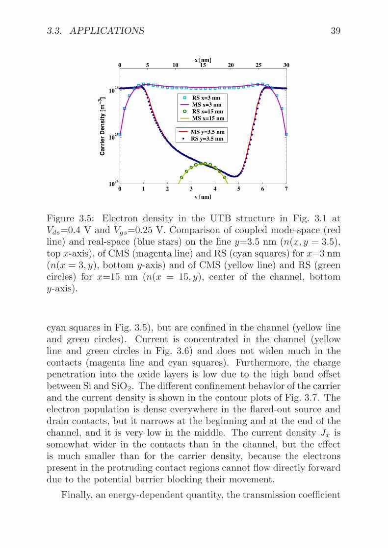
According to Eq. (3.18), in the absence of correlation terms, theelectron density exhibits a non-physical behavior at the interface be-tween wide and narrow regions, as illustrated in Fig. 3.4: a cut alongthe transport axis is extracted for Vds = Vgs=0. The red line resultsfrom the correct Eq. (3.15) and the blue line from the incompleteEq. (3.18). The inset clearly shows the appearance of a spurious spikein the electron distribution at the interface between the flared-outsource and the squeezed channel. The same discrepancy occurs onthe other side of the channel. It is evident that mode correlation ef-fects smooth the charge density, enabling a self-consistent solution ofGreen’s function and Poisson’s equation. Consequently, it is neces-sary to compute the carrier density as given by Eq. (3.15), if strongmode coupling effects are present. On the right side of Fig. 3.4, acomparison between CMS and RS for two different electron densitycuts, one along the line y=3.5 nm (red line and blue stars) and theother along x=3 nm (magenta line and blue squares), confirms thevalidity of the coupled mode-space approach when no bias is appliedto the nanoscale transistor.
When the device is strongly biased, more coupling effects are ex-pected, because the electrons injected in the source interact with many

38 CHAPTER 3. EFFECTIVE MASS APPROXIMATION
0 10 20 300
2
4
6
8
10
12
14x 10
25
x [nm]
Car
rier
Den
sity
[m
−3]
MS y=3.5 nnRS y=3.5 nm
0 2 4 6
0
2
4
6
8
10
12
14
y [nm]
MS x=3 nmRS x=3 nm
0 10 20 300
2
4
6
8
10
12
14x 10
25
x [nm]
Car
rier
Den
sity
[m
−3]
MS new y=3.5 nmMS old y=3.5 nm
2 4 6y [nm]
MS new x= 3nmMS old x=3 nm
4.5 5 5.53
4
5
6
7x 10
25
Figure 3.4: Electron density profile in the UTB from Fig. 3.1 at Vds =Vgs=0 V. (left) Comparison of two different CMS solutions along theline y=3.5 nm (device axis of symmetry, n(x, y = 3.5), blue and redlines) and along the line x=3 nm (yellow and magenta lines) obtainedwithout mode correlations (lines labeled MS old) and with them (lineslabeled MS new). The inset is an enlargement of the interface betweenthe flared-out source and the channel. (right) Comparison for y=3.5nm (n(x, y = 3.5), bottom x-axis) of CMS (red line) and RS (bluestars) calculations and for x=3 nm (n(x = 3, y), in the source, topy-axis) of CMS (magenta line) and RS (cyan squares) simulations.
modes before reaching the drain. Therefore, Figs. 3.5 and 3.6 repre-sent electron and current density (Jx) for Vgs=0.25 V and Vds=0.4 Valong different cut lines. Both CMS and RS solutions are depictedfor the lines y=3.5 nm (symmetry axis), x=3 nm (in the source), andx=15 nm (channel center). Excellent agreement (less than 2% relativedifference between CMS and RS) is achieved between the two curves.One sees that the source-channel (x=5 nm) and channel-drain (x=25nm) interfaces are smooth for both carrier and current densities, con-firming that coupled mode effects are treated correctly. The accuracyof the CMS approach is also verified when bias is applied.
Electrons occupy the full width of the contacts (magenta line and
3.3. APPLICATIONS 39
0 5 10 15 20 25 30
1024
1025
1026
y [nm]
Car
rier
Den
sity
[m
−3]
MS y=3.5 nmRS y=3.5 nm
0 1 2 3 4 5 6 7
x [nm]
RS x=3 nmMS x=3 nmRS x=15 nmMS x=15 nm
Figure 3.5: Electron density in the UTB structure in Fig. 3.1 atVds=0.4 V and Vgs=0.25 V. Comparison of coupled mode-space (redline) and real-space (blue stars) on the line y=3.5 nm (n(x, y = 3.5),top x-axis), of CMS (magenta line) and RS (cyan squares) for x=3 nm(n(x = 3, y), bottom y-axis) and of CMS (yellow line) and RS (greencircles) for x=15 nm (n(x = 15, y), center of the channel, bottomy-axis).
cyan squares in Fig. 3.5), but are confined in the channel (yellow lineand green circles). Current is concentrated in the channel (yellowline and green circles in Fig. 3.6) and does not widen much in thecontacts (magenta line and cyan squares). Furthermore, the chargepenetration into the oxide layers is low due to the high band offsetbetween Si and SiO2. The different confinement behavior of the carrierand the current density is shown in the contour plots of Fig. 3.7. Theelectron population is dense everywhere in the flared-out source anddrain contacts, but it narrows at the beginning and at the end of thechannel, and it is very low in the middle. The current density Jx issomewhat wider in the contacts than in the channel, but the effectis much smaller than for the carrier density, because the electronspresent in the protruding contact regions cannot flow directly forwarddue to the potential barrier blocking their movement.
Finally, an energy-dependent quantity, the transmission coefficient

40 CHAPTER 3. EFFECTIVE MASS APPROXIMATION
5 10 15 20 25 30
y [nm]
MS y=3.5 nmRS y=3.5 nm
0 1 2 3 4 5 6 70
2
4
6
8
10
12
14x 10
10
x C
ompo
nent
of
Cur
rent
Den
sity
[A
/m2 ]
MS x=3 nmRS x=3 nmMS x=15 nmRS x=15 nm
x [nm]
Figure 3.6: x-component of the current density along the trans-port axis in the UTB from Fig. 3.1 at Vds=0.4 V and Vgs=0.25 V.Comparison of CMS (red line) and RS (blue stars) for y=3.5 nm(Jx(x, y = 3.5), top x-axis), of CMS (magenta line) and RS (cyansquares) for x=3 nm (Jx(x = 3, y), bottom y-axis), and of CMS (yel-low line) and RS (green circles) for x=15 nm (Jx(x = 15, y), bottomy-axis).
from source to drain, is calculated in coupled mode-space and in realspace for Vgs=0.25 V and Vds=0.4 V. The results are depicted inFig. 3.8 for two different effective masses in y-direction: 1. my isaligned with the longitudinal mass ml (red line and blue circles) and2. my is aligned with the transverse one mt (yellow line and greensquares). The CMS and RS curves are almost identical at low energyand slightly diverge at high energy, because an incomplete basis is usedto expand the Green function in mode-space. For higher energies, theincompleteness of the basis becomes more important, since only thelowest energetic eigenmodes of the αi’s were kept to form the basis.
3.3.2 Three-dimensional device: Si Nanowire
The second structure simulated in coupled mode-space is the three-dimensional Si nanowire from Fig. 3.2. It has a total length Ltot=30nm, composed of two flared-out contacts, the source (length Ls=5

3.3. APPLICATIONS 41
−12
−10
− 8
− 6
− 4
− 2
x 10 25
0 5 10 15 20 25 300
2
4
6
x [nm]
y [n
m]
0 5 10 15 20 25 300
2
4
6
x [nm]
y [n
m]
−14
−12
−10
− 8
− 6
− 4
− 2
x 10 10
SiO2
SiO2
SiO2
SiO2
Figure 3.7: Contour plot of the electron density (top, n(x, y), unit:m−3) and of the current density in the transport direction (bottom,Jx(x, y), unit: A/m2) for the UTB from Fig. 3.1 at Vds=0.4 V andVgs=0.25 V in coupled mode-space.
0 0.1 0.2 0.3 0.4 0.5 0.60
0.5
1
1.5
2
2.5
3
3.5
4
E [eV]
Tra
nsm
issi
on
MS my=0.98m
oMS m
y=0.19m
oRS m
y=0.98m
oRS m
y=0.19m
o
Figure 3.8: Transmission coefficient from source to drain for the devicefrom Fig. 3.1. CMS solutions (red and yellow lines) are comparedto RS calculations (blue circles and green squares) for two differenteffective masses in the y direction, the longitudinal my = 0.98mo andthe transverse my = 0.19mo.

42 CHAPTER 3. EFFECTIVE MASS APPROXIMATION
nm, height htot=5.6 nm, and width wr=7 nm) and the drain (lengthLd= 5nm, same height and width as source) and a buried channel(thickness tc=3 nm, height hc=4 nm, length Lc=20 nm, extendingfrom x=5 nm to x=25 nm, from y=2 nm to y=5 nm, and from z=0nm to z= 4nm) surrounded by three 1.6 nm thick SiO2 layers (tox=1.6nm). The buried oxide below the device is modeled by hard wall(Dirichlet) boundary conditions. The triple-gate contact is situatedin the middle of the channel, covering the left, right, and upper sidesof the nanowire together with the SiO2 layers. The lower right cornerof the device on the source side is artificially removed to offer a viewon the epitaxial structure. The transition from the wide, highly-dopedsource and drain to the squeezed channel is perturbed in the y (totalwidth: 0≤ y ≤7 nm, channel: 2≤ y ≤5 nm) and z (total height: 0≤z ≤5.6 nm, channel: 0≤ z ≤4 nm) directions. Therefore, strong modecoupling effects are expected at x=5 nm (source-channel interface) andx=25 nm (channel-drain). Effective transport occurs only along thex-axis (0≤ x ≤30 nm) due to the absence of leakage current throughthe gate contacts.
The simulation scheme for the 3D MOSFET from Fig. 3.2 fol-lows the procedure outlined in Section 3.3.1. However, there aretwo elements that increase the computational burden. The eigen-functions generating the incomplete basis are two-dimensionally con-fined and secondly, Poisson’s equation must be solved in 3D. There-fore, if the previously open direction z is now discretized with Nz
points, the transformation matrix U defined in Eq. (3.12) is of size(NxNyNz)× (NxNm), but the mode space Hamiltonian Hms remainsof size (NxNm) × (NxNm). It is worth noting that the number ofmodes Nm that needs to be considered in 3D is usually larger thanin 2D because the energy spacing between them is lower. Carrier andcurrent density are obtained with Eqs. (3.15)-(3.17), where the modesφin(yj) become φin(yjzk) to account for the third dimension z. Addi-tionally, Jz, the current in the z direction is calculated similarly to Jxand Jy. No real-space solution of the 3D device has been attempteddue to the high computational resources required.
Figure 3.9 shows the simulation results for the current-voltagecharacteristics in the nanowire MOSFET. On the left, the total cur-rent ID (integral of the current density Jx over the nanowire crosssection, unit µA) from drain to source as function of drain voltage
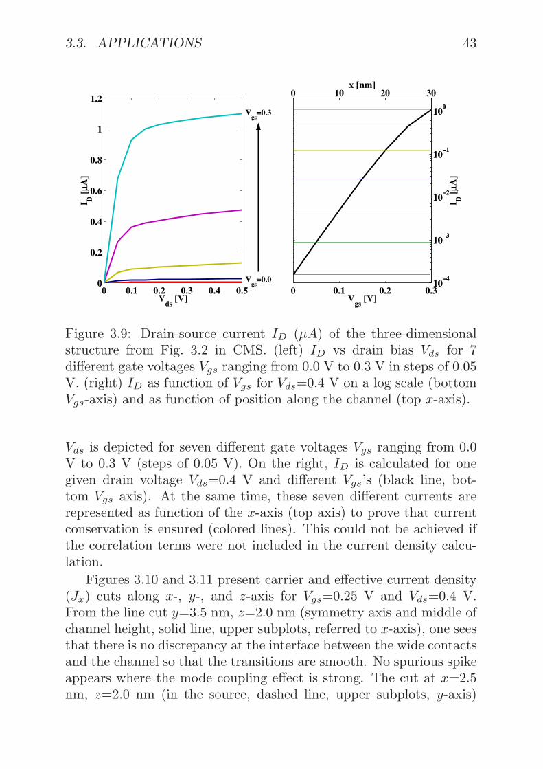
3.3. APPLICATIONS 43
0 0.1 0.2 0.3 0.4 0.50
0.2
0.4
0.6
0.8
1
1.2
Vds
[V]
I D [
µA]
0 0.1 0.2 0.310
−4
10−3
10−2
10−1
100
Vgs
[V]
0 10 20 30
10−4
10−3
10−2
10−1
100
x [nm]
I D [
µA]
Vgs
=0.3
Vgs
=0.0
Figure 3.9: Drain-source current ID (µA) of the three-dimensionalstructure from Fig. 3.2 in CMS. (left) ID vs drain bias Vds for 7different gate voltages Vgs ranging from 0.0 V to 0.3 V in steps of 0.05V. (right) ID as function of Vgs for Vds=0.4 V on a log scale (bottomVgs-axis) and as function of position along the channel (top x-axis).
Vds is depicted for seven different gate voltages Vgs ranging from 0.0V to 0.3 V (steps of 0.05 V). On the right, ID is calculated for onegiven drain voltage Vds=0.4 V and different Vgs’s (black line, bot-tom Vgs axis). At the same time, these seven different currents arerepresented as function of the x-axis (top axis) to prove that currentconservation is ensured (colored lines). This could not be achieved ifthe correlation terms were not included in the current density calcu-lation.
Figures 3.10 and 3.11 present carrier and effective current density(Jx) cuts along x-, y-, and z-axis for Vgs=0.25 V and Vds=0.4 V.From the line cut y=3.5 nm, z=2.0 nm (symmetry axis and middle ofchannel height, solid line, upper subplots, referred to x-axis), one seesthat there is no discrepancy at the interface between the wide contactsand the channel so that the transitions are smooth. No spurious spikeappears where the mode coupling effect is strong. The cut at x=2.5nm, z=2.0 nm (in the source, dashed line, upper subplots, y-axis)

44 CHAPTER 3. EFFECTIVE MASS APPROXIMATION
0 5 10 15 20 25 30
1023
1024
1025
1026
1027
y [nm]
Ele
ctro
n D
ensi
ty [
m−3
] y=3.5 nm, z=2.0 nm
0 1 2 3 4 5 6 7
x [nm]
x=2.5 nm, z=2.0 nmx=15 nm, z=2.0 nm
0 1 2 3 4 510
23
1024
1025
1026
1027
z [nm]
Ele
ctro
n D
ensi
ty [
m−3
] x=2.5 nm, y=3.5 nmx=15 nm, y=3.5 nm
Figure 3.10: Electron density for the nanowire from Fig. 3.2 atVds=0.4 V and Vgs=0.25 V in CMS. (upper) The solution at y=3.5 nm(symmetry axis) and z=2.0 nm (middle of channel height) (n(x, y =3.5, z = 2.0), red line, top x-axis), at x=2.5 nm (middle of the drain)and z=2.0 nm (n(x = 2.5, y, z = 2.0), magenta line, bottom y-axis),and at x=15 nm (channel center) and z=2.0 nm (n(x = 15, y, z = 2.0),yellow line, bottom y-axis) are shown. (lower) Density profile alongthe lines x=2.5 nm, y=3.5 nm (n(x = 2.5, y = 3.5, z), green line) andx=15 nm, y=3.5 nm (n(x = 15, y = 3.5, z), blue line).
shows that electrons occupy the full width of the contacts (here thesource), but that the current contribution from the flared-out regionsis lower than the one from the middle, as in Fig. 3.6. This is notsurprising, because one finds exactly the UTB structure in Fig. 3.1,if the nanowire in Fig. 3.2 is cut at z=2.0 nm. Therefore, electronand current densities along the line x=15 nm, z=2.0 nm (channelcenter, dashed-dotted line, upper subplots, y axis) show the samecharacteristics as for the two-dimensional device. They are stronglyconfined in the channel with almost no penetration into the oxidelayers.

3.3. APPLICATIONS 45
5 10 15 20 25 30
y [nm]
x C
urre
nt D
ensi
ty [
A/m
2 ] y=3.5 nm, z=2.0 nm
0 1 2 3 4 5 6 70
5
10
15x 10
10x [nm]
x=2.5 nm, z=2.0 nmx=15 nm, z=2.0 nm
0 1 2 3 4 50
5
10
15x 10
10
z [nm]
x C
urre
nt D
ensi
ty [
A/m
2 ] x=2.5 nm, y=3.5 nmx=15 nm, y=3.5 nm
Figure 3.11: x-component of the current density for the NW fromFig. 3.2 at Vds=0.4 V and Vgs=0.25 V in CMS. (upper) The results fory=3.5 nm and z=2.0 nm (Jx(x, y = 3.5, z = 2.0), red line, top x-axis),for x=2.5 nm and z=2.0 nm (Jx(x = 2.5, y, z = 2.0), magenta, bottomy-axis), and for x=15 nm and z=2.0 nm (Jx(x = 15, y, z = 2.0),yellow line, bottom y-axis) are plotted. (lower) The lines x=2.5 nmand y=3.5 nm (Jx(x = 2.5, y = 3.5, z), green line) and x=15 nm andy=3.5 nm (Jx(x = 15, y = 3.5, z), blue line) are shown.
Finally, a cut along the z-axis is given in the lower subplot ofFigs. 3.10 and 3.11. The 4 nm high channel is covered by an oxidelayer with tox=1.6 nm, the source and drain contacts (height of 5.6nm) are made of pure n-doped Si. While electrons and current fillthe total device height in the contacts (green line, x=2.5 nm, y=3.5nm), they are squeezed in the channel (blue line x=15 nm, y=3.5nm). This double confinement (y and z) can be efficiently treated incoupled mode-space, but only with mode correlation terms.
The above observations are confirmed by Fig. 3.12. It shows thecontour plot of the electron density in the planes z=2.0 nm (uppersubplot) and y=3.5 nm (lower plot). Mobile charges are confined due

46 CHAPTER 3. EFFECTIVE MASS APPROXIMATION
0 5 10 15 20 25 300
2
4
6
x [nm]
y [n
m]
0 5 10 15 20 25 300
2
4
6
x [nm]
z [n
m]
−1. 5
−1.0
−0. 5
x 10 26
−15
−10
−5
x 1025
SiO2
SiO2
SiO2
Figure 3.12: Contour plot of the electron density (unit: m−3) for thedevice from Fig. 3.2 at Vds=0.4 V and Vgs=0.25 V, in the planes z=2.8nm (middle of total height htot, n(x, y, z = 2.8), top) and y=3.5 nm(n(x, y = 3.5, z), bottom).
to the different oxide layers surrounding the nanowire channel, butelectrons extend over the total width and height of the source anddrain regions.
3.4 Discussion
In this Section, the advantages and disadvantages of the coupledmode-space approach and the possibility of including scattering andmore sophisticated band structure models in the formalism are dis-cussed. The choice of an incomplete basis to expand the nonequilib-rium Green’s function leads to a substantial reduction of the computa-tional burden. A factor (Ny/Nm), where Nm is the number of consid-ered modes andNy the number of discretization points in the directionof confinement, is gained in the matrix size for two-dimensional struc-tures. In the present simulations, a Poisson iteration (time to calculatecarrier and current densities and to recompute the device potential)

3.5. SUMMARY 47
lasts 105 s for mode-space and 1120 s for real-space at Vgs=Vds=0V and with the same energy grid. For the three-dimensional tran-sistor, a mode-space Poisson iteration lasts 830 s at Vgs=Vds=0 V.However, the mode-space method has two important drawbacks. Itworks only for structures with a strong confinement, where only fewmodes are occupied, so that Nm Ny. Otherwise, if many modesare involved in the carrier and current density calculation, there is noreason to work in mode-space because the time required to solve theSchrodinger equation in the direction(s) of confinement is not compen-sated by the reduction of the matrix size to deal with. In this case, areal-space solution becomes advantageous. In addition, the real-spacesolution takes the gate leakage current into account[23], which is dif-ficult in mode-space, constituting its second restriction. To obtainthe eigenfunctions in the direction of confinement, Dirichlet bound-ary conditions are applied, but in the gate region, the inclusion ofa leakage current implies open boundary conditions. A combinationof both approaches is not evident. It is worth stressing that coupledmode-space calculations do not only deliver currents in the transportdirection, but they also describe the particle flow in the other direc-tions. This is not an effective current, however, because it vanisheswhen integrated over the entire device structure.
A mode-space approach (coupled or not) is not adapted to in-clude accurate bandstructure models in the device simulations. Inthe effective mass approximation, electron and current density canbe expressed in an energy-independent and incomplete basis. This isnot the case for k·p or tight-binding methods that require more basiscomponents, different for each injection energy. In effect, due to thenon-parabolicity of the semi-infinite reservoir band structures, the in-jected, reflected or transmitted states have different wave functionsfor each wave vector[46] (or injection energy).
3.5 Summary
In this Chapter, a detailed derivation of the coupled mode-space ap-proach in the Nonequilibrium Green’s Function formalism was pre-sented. It was pointed out that the omission of some important modecorrelation terms in the carrier and current density calculation leads

48 CHAPTER 3. EFFECTIVE MASS APPROXIMATION
to non-physical discrepancies at positions where strong mode couplingeffects occur, for example at the interface between a wide and a nar-row region. Within two applications, it was proved that the completeNEGF treatment removes these inconsistencies. A two-dimensionalultra-thin body and a three-dimensional nanowire transistor, bothwith flared-out contacts and a squeezed channel were studied. Aself-consistent solution of Poisson’s and NEGF equations was madepossible without loosing any physical accuracy. A real-space solu-tion confirmed the exactitude of the coupled mode-space method fortwo-dimensional nanostructures. Because the mode-space approachdoes not work with sophisticated bandstructure model, a new methodneeds to be developed for full-band quantum transport.

Chapter 4
Bandstructure Model
4.1 Introduction
Any bandstructure model should reproduce accurately the experimen-tally verified energy band gaps and effective masses of semiconductorcrystals. If these material properties strongly diverge from their mea-sured values, neither the energies of quantized states nor their con-finement can be modeled properly.
The first step consists in finding this accurate bandstructure model.The effective mass approximation works well in the vicinity of con-duction band minima or valence band maxima, but it does not alwaysensure a correct calculation of the quantization levels in nanostruc-tures. During the last two decades empirical tight-binding methodshave become the primary choice of many researchers. In effect, theyhave the ability to correctly reproduce band gaps and effective masseswith a localized atomistic orbital basis.
The empirical tight-binding method was first proposed by Slaterand Koster in 1954[32]. During many years, for computational rea-son, only eight orbitals were kept, one s- and three p-, each of themwith spin up and spin down polarizations (sp3). The approach wasenhanced thirty years later by the inclusion of an excited s-like state,s∗[33] (sp3s∗). This additional feature allowed a better descriptionof the conduction band of diamond and zincblende semiconductors
49

50 CHAPTER 4. BANDSTRUCTURE MODEL
along [100]. Much more recently, excited d-orbitals (sp3d5s∗) wereintroduced to a nearest-neighbor approach, improving the X-valleytransverse masses[47].
With the nearest-neighbor sp3d5s∗ empirical tight-binding method,one is therefore able to reproduce the complete bulk bandstructure[34]within a reasonable tolerance. Furthermore, its atomistic descriptionof the simulation domain is advantageous at the nanometer scale. Inthis context, phenomena such as interface roughness, alloy disorder,heterostructures, or impurity scattering can be treated rigorously.
4.2 Theory
For a given crystal structure, the semi-empirical tight-binding methodconsists in finding energy bands En and coefficients Cn of a linearcombination (or Bloch sum) of atomic orbitals φn(r − Ri). Thesefunctions are located on the various atoms i at position Ri in thecrystal. n refers to the band quantum number. The periodicity ofthe simulated structure will determine the form of the Bloch sumconstructed from the orbital functions.
The primitive unit cell characterizes the atomic fitting of a semi-conductor crystal. It is defined by the number N of atoms it containsand their type α (cation or anion), by its primitive vectors a1 to aN(position of the atoms in the cell), and by its basis (or translation)vectors v1, v2, and v3. In the nearest neighbor approximation all theatoms are connected to four neighbors, except at the boundary of thesimulation domain, where dangling bonds can be found. A primitiveunit cell with N atoms has therefore 4N different bond vectors bαi (iruns from 1 to 4, α determines the atom the bond starts from).
4.2.1 Bulk
For bulk structures (periodicity in x, y, and z), the Bloch sum takesthe following form
ψ(r) =∑σ,α,k
Cασ (k)
∑Rα
i
φασ(r−Rαi )eik·R
αi

4.2. THEORY 51
|ψ〉 =∑σ,α,k
Cασ (k)|kσα〉 (4.1)
where σ is the orbital type (s, p, d, s∗), α is the atom type (cation1 to cation N/2, anion 1 to anion N/2), and k is a three-dimensionalwave vector. The wave function |ψ〉 is the solution of the stationarySchrodinger equation for bulk crystal, because |kσα〉 fulfills the Blochtheorem. With the Hamilton H0 in Eq. (2.36) one has
H0|ψ〉 = E|ψ〉. (4.2)
The tight-binding Hamilton matrix H is obtained by multiplying theleft- and the right-hand side of Eq. (4.2) with 〈kσα|. To calculate thematrix elements of H, the two center approximation is applied andthe orbital functions φασ(r−Rα
i ) are orthogonalized (Lowdin’s orbitalfunctions)[32]. After some straightforward algebra, the general formof the bulk tight-binding problem can be written as
(Hαα −E(k))Cα(k) +4∑
i=1
Vαβ(bαi )Cβ(k)eik·bαi = 0. (4.3)
In Eq. (4.3), all the orbitals σ are cast into a single quantity so thatHαα and Vαβ(bαi ) are matrices of size tb × tb, Cα(k) and E(k) arevectors of size tb. The parameter tb is the number of different orbitalstaken into account in the calculation, for example 10 in the sp3d5s∗
model without spin and 20 with spin.Hαα is the on-site energy of an atom α. It is a diagonal matrix
with elements Eαs (on-site energy of the s orbital for an atom of type
α), Eαp (three times), Eα
d (five times), and Eαs∗ . The off-diagonal
elements are equal to 0, except when spin-orbit coupling is present.The matrix Vαβ(bαi ) represents the coupling between an atom
of type α and an atom of type β connected by the bond bαi . Ifα stands for a cation, β must be an anion and vice versa (nearest-neighbor approximation). For instance, the matrix element V αβ
x,xy(bαi ),
i.e. the overlap integral between an orbital pαx and an orbital dβxy, isapproximated in terms of two integrals: one between a pσ orbital onthe first atom and a dσ on the second, V αβ
pdσ; and one between a pπorbital on the first atom and a dπ on the second, V αβ
pdπ. Since the
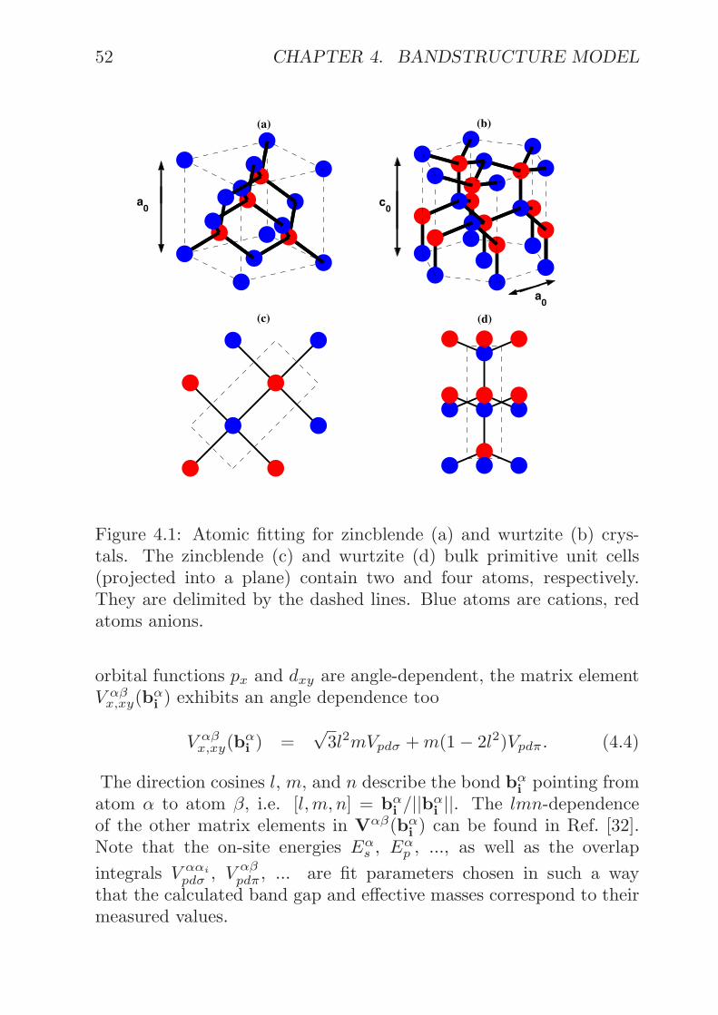
52 CHAPTER 4. BANDSTRUCTURE MODEL
a0 c
0
a0
(a) (b)
(c) (d)
Figure 4.1: Atomic fitting for zincblende (a) and wurtzite (b) crys-tals. The zincblende (c) and wurtzite (d) bulk primitive unit cells(projected into a plane) contain two and four atoms, respectively.They are delimited by the dashed lines. Blue atoms are cations, redatoms anions.
orbital functions px and dxy are angle-dependent, the matrix elementV αβx,xy(b
αi ) exhibits an angle dependence too
V αβx,xy(b
αi ) =
√3l2mVpdσ +m(1 − 2l2)Vpdπ. (4.4)
The direction cosines l, m, and n describe the bond bαi pointing fromatom α to atom β, i.e. [l,m, n] = bαi /||bαi ||. The lmn-dependenceof the other matrix elements in Vαβ(bαi ) can be found in Ref. [32].Note that the on-site energies Eα
s , Eαp , ..., as well as the overlap
integrals V ααi
pdσ , V αβpdπ, ... are fit parameters chosen in such a way
that the calculated band gap and effective masses correspond to theirmeasured values.

4.2. THEORY 53
x
y z
x y
z
Quantum Well Quantum Wire
Figure 4.2: Schematic view of a quantum well with infinite dimensionsalong x and y and confinement along z (left) and of a quantum wirewith confinement in the y and z directions and infinite dimension alongx (right). The atomic unit cell of the structures are also depicted; blueand red points represent atoms.
Figure 4.1 shows the atomic fitting of two crystal classes, zincblendeon the left and wurtzite on the right. A projection of their primi-tive unit cell is given in the lower part of the plot. Zincblende hastwo atoms in its primitive unit cell so that the eigenvalue problem inEq. (4.3), put into a matrix H, is of size (2tb) × (2tb). The wurtzitecell contains four atoms leading to a matrix H of size (4tb) × (4tb).
4.2.2 Nanostructures
The transition from infinite (bulk) to one- or two-dimensionally con-fined nanostructures is computationally straight forward. The atomicon-site energies as well as the connections to the nearest neighborsare modeled with the bulk material parameters. Hard wall bound-ary conditions are applied to the surface atoms by “passivating” theirdangling-bonds[48]. The difficulty resides in the construction of theprimitive unit cell of these confined structures.
In Fig. 4.2 an ideal ultra-thin body (or quantum well) with growthdirection along z (left) and an ideal quantum wire with confinementin y and z (right) are shown. Their primitive unit cells are composedof a number of atoms (blue and red points) that depends on the di-

54 CHAPTER 4. BANDSTRUCTURE MODEL
mension of the structures and on the growth direction, contrary tobulk crystals, where this number remains constant.
The primitive vectors a1 to aN, the basis vectors v1, v2, and v3,and the bond vectors bαi are defined for crystal axis x aligned with[100], y with [010], and z with [001]. If x is aligned with x=[ax,bx,cx],y becomes aligned with y=[ay,by,cy] (ay, by, and cy can be freelychosen as long as the scalar product x · y=0), and z is aligned withz=[az,bz,cz]=x x y (cross product). To express the primitive unit cell,the basis, and the bond vectors in this new basis, a rotation matrixR is introduced
R =
ax/||x|| ay/||y|| az/||z||bx/||x|| by/||y|| bz/||z||cx/||x|| cy/||y|| cz/||z||
−1
. (4.5)
The new quantities are obtained by multiplying the old ones with R.For example v1 = R·v1. This is a necessary step to change the growthdirection of a quantum well or the transport direction of a quantumwire. The rotated primitive unit cell is shifted with the new vectorsv1,2,3 to construct a structure. For the rest of this Chapter the tilde[˜] are omitted, but the vectors can be expressed in any basis.
Ultra-Thin Body (Quantum Well)
For an ultra-thin body (UTB) the Bloch sum in Eq. 4.1 is modifiedto account for the confinement along the z axis, where the structureperiodicity is broken
ψ(r) =∑
σ,α,kt
∑zk
Cασ (zk,kt)
∑Rα
ti
φασ(r− {Rαti, zk})eikt·Rα
ti
|ψ〉 =∑
σ,α,kt
∑zk
Cασ (zk,kt)|ktσα〉. (4.6)
The position Rαi of the atoms is split into a transverse component
Rαti and a longitudinal component zk, parallel to the growth direc-
tion. Consequently the wave vector k becomes kt = {kx, ky}. If theHamiltonian H0 in Eq. (2.36) is applied to |ψ〉 and if the same ap-proximations as in the bulk case are made (Lowdin’s orbitals, nearest-

4.2. THEORY 55
neighbor, two center integrals, ...), one obtains
(Hαα −E(kt))Cα(zk,kt) +4∑
i=1
Vαβ(bαi )Cβ(zk + bαzi,kt)eikt·{bαxi,b
αyi} = 0. (4.7)
The matrices Hαα and Vαβ(bαi ) are exactly the same as in Eq. (4.3).However, there are two essential differences. First, the eigenvalueproblem in Eq. (4.7) must be solved in a two-dimensional BrillouinZone instead of a three-dimensional one. Secondly, the different zkpositions of the atoms along the growth direction must be determined.This is done by choosing a start position zk = z0 where the first atomof type α is placed. The coordinates of the other atoms must be largerthan z0 and smaller than z0 + Lz where Lz is the width of the UTB.
Four different bonds bαi start from the first atom at zk = z0 andconnect it to atoms situated at z0 + bαzi (bαzi is the z-component of thebond vectors). All the atoms with z0+bαzi ≥ z0 are kept, because theyare part of the UTB. Then one goes to the new atom with the smallestz0 + bαzi and repeat the procedure above. This operation is redone forall the atoms present in the structure until only z-components largerthan z0 +Lz are found. Thus an atomic chain is built that representsthe projection of the UTB unit cell onto a single line.
Examples of atomic chains are given in Fig. 4.3 for 2 nm wide Siquantum wells and growth directions along [001] (15 atoms), [110] (22atoms), [111] (14 atoms), and [113] (25 atoms). If NA is the number ofatoms in the UTB unit cell, the eigenvalue problem has a size (NAtb)x (NAtb).
It is possible that more than one atom of the same type is situatedat a given zk. Then the bonds connecting zk to its neighbors aretwofold degenerate. This is the case for the [001] growth directionwhere two anions (red points) are situated at zk = 0 nm, two cations(blue points) at zk = a0/4 = 0.136 nm, two anions at zk = a0/2 =0.271 nm, and so on. This situation is described in Refs. [49, 50].
Nanowire
Ideal nanowires are confined in two directions, for example y andz, and are periodic along x. Accordingly, the bulk Bloch sum in
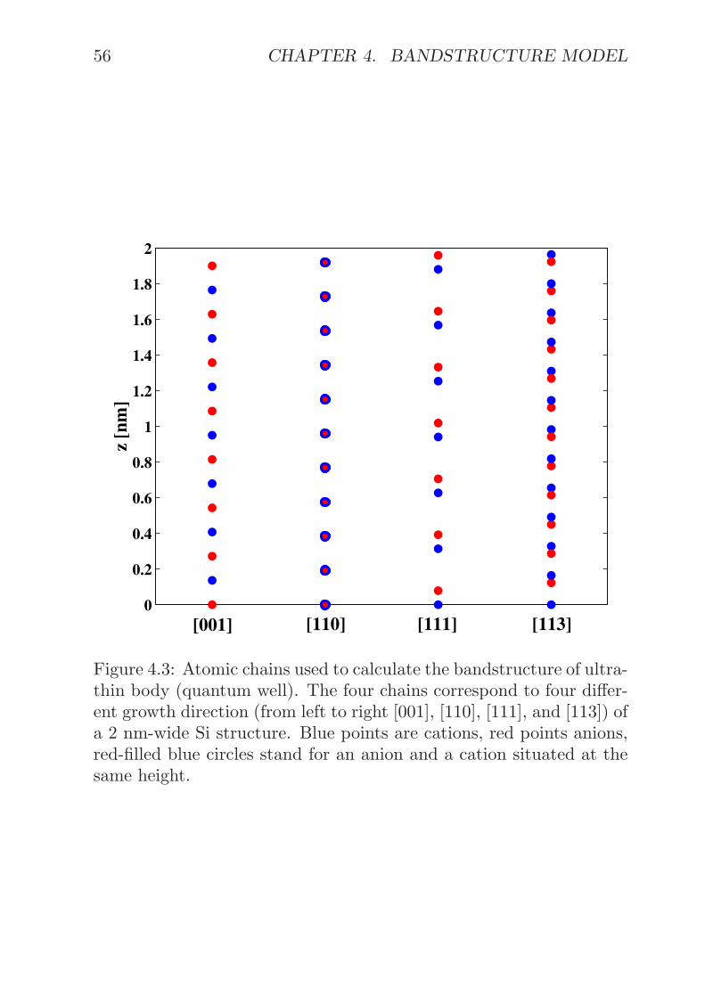
56 CHAPTER 4. BANDSTRUCTURE MODEL
0
0.2
0.4
0.6
0.8
1
1.2
1.4
1.6
1.8
2
z [n
m]
[001] [113] [110] [111]
Figure 4.3: Atomic chains used to calculate the bandstructure of ultra-thin body (quantum well). The four chains correspond to four differ-ent growth direction (from left to right [001], [110], [111], and [113]) ofa 2 nm-wide Si structure. Blue points are cations, red points anions,red-filled blue circles stand for an anion and a cation situated at thesame height.

4.2. THEORY 57
Eq. (4.1) is reduced to a sum over the kx-component of k and overthe x-component of the atom position Ri. This gives
ψ(r) =∑
σ,α,kx
∑yj ,zk
Cασ (yj , zk, kx)
∑xi
φασ(r− {xi, yj , zk})eikxxi
|ψ〉 =∑
σ,α,kx
∑yj ,zk
Cασ (yj , zk, kx)|kxσα〉 (4.8)
for the wave function |ψ〉 and
(Hαα −E(kx))Cα(yj , zk, kx) +4∑
i=1
Vαβ(bαi )Cβ(yj + bαyi, zk + bαzi, kx)eikxb
αxi = 0 (4.9)
for the wire equation (Lowdin’s orbitals, nearest neighbor, and twocenter approximations are applied as in the bulk and in the UTBcases). Equation (4.9) is constructed with the same matrices Hαα
and Vαβ(bαi ) as in Eqs. (4.3) and (4.7). However, it must be solvedin a one-dimensional, kx-dependent, Brillouin Zone.
The positions yj and zk of the atoms describe the cross section ofthe nanowire, i.e. what would be seen if one looks through a nanowirealong its x-axis. To find the yj and zk, the nanowire cross sectionis delimited by its corner points, and the crystal axis x, y, and zare chosen. The basis vectors, the primitive vectors, and the bondvectors are expressed in the resulting basis. Since one deals with atwo-dimensional structure (dependence on yj and zk), the y- and z-components of the different vectors are kept. For example v1 → v1t ={v1y, v1z}. Note that v1t, v2t, and v3t are linearly dependent vectors.
The two-dimensionally projected bulk primitive unit cell, charac-terized by its primitive vectors a1t to aNt, is translated by linearcombinations of v1t and v2t, n1v1t + n2v2t. The integers n1 and n2
vary from −∞ to +∞. For each (n1, n2) pair, the N atoms constitut-ing the bulk primitive unit cell are checked to be inside or outside thepreliminary defined nanowire cross section. If an atom is inside thesimulation domain, its y- and z- components are kept, otherwise theyare disregarded. The retained coordinates form the projection of thenanowire unit cell, also called slab. If there are NA atoms per slab,the bandstructure eigenvalue problem is of size (NAtb) x (NAtb).

58 CHAPTER 4. BANDSTRUCTURE MODEL
4.2.3 Strain
Mechanical strain is present in a wide variety of material systems.When the lattice constant of a semiconductor layer is smaller or largerthan the lattice constant of the material it is grown on, displacementof the atoms from their original unstrained positions is observed.
In such strained systems the matrix elements of Vαβ(bαi ) in Eqs.(4.3), (4.7), and (4.9) are altered due to the change of bαi in termsof both length and angle. Bond angle alterations are fully taken intoaccount in the Slater-Koster table through the direction cosines l, m,and n[32]. Changes of the bond length are obtained by scaling thematrix elements, for example Vx,xy in Eq. (4.4) by a factor (d0/d)η,where d0 and d are the ideal and the strained bond length, respectively.This generalization of Harrison’s scaling law[51] means that Vx,xy →Vx,xy × (d0/d)η where η is a fit parameter.
Since the tight-binding atomic orbitals are not true atomic or-bitals, the diagonal matrix elements of Hαα in Eqs. (4.3), (4.7), and(4.9), too, are influenced by atom displacements[52]
Eασ = Eα
σ +4∑
i=1
∑γ
Cαβγ,σ
[V βαγ,σ (bαi )
]2 − [V βαγ,σ (bαi )
]2Eασ + Eβ
γ
. (4.10)
The strain-modified quantities carry a tilde. The parameters α andβ are the atom types (cation or anion), σ and γ are the orbital types(s, p, d, and s∗), and Cαβ
γ,β are diagonal parameter shift constants (fitparameters).
The displacement of the atoms due to strain should be calculatedaccurately by minimizing the total strain energy[53] present in thematerial system. However, as a first approximation, biaxial (uniaxial)strain in the x and y (z) direction can be assumed, if a very thinlayer (lattice constant a0) is grown on a thick reference layer (latticeconstant aref0 ) along the z direction. One has therefore[54]
εxx = εyy =aref0 − a0a0
εzz = −Dεxx, (4.11)
where εxx, εyy, and εzz are the relative displacements of the atomsalong x, y, and z, respectively. D depends on the elastic constants

4.3. RESULTS 59
c11, c12, and c44 and on the growth direction of the thin layer. Thebasis vectors, the primitive vectors, and the bond vectors are thenmultiplied by the strain matrix S
S =
1 + εxx 0 0
0 1 + εyy 00 0 1 + εzz
. (4.12)
If the growth direction z differs from [001], the unit cell vectors ai,vi, and bαi are first rotated with the matrix R in Eq. (4.5) and thenstrained with S, i.e. {ai,vi,bαi } → S ·R · {ai,vi,bαi }.
In addition to the macroscopic strain described by S, internal dis-placements of the atoms should be considered, if z is different from[001][55, 56]. This effect tends to reduce the nearest neighbor centralforce of the system[57].
Finally, in the bulk case, if the uniaxial component of the macro-scopic strain is not aligned with z, the x, y, and z axis are transformedin such a way that z becomes aligned with the uniaxial componentof the strain. This is achieved with Eq. (4.5). Then the diagonalstrain tensor in Eq. (4.12) is applied to the basis vectors, to the prim-itive vectors, and to the bond vectors, that are transformed back tothe original basis with the inverse of the rotation matrix. The re-sulting strain tensor S is a matrix with non-diagonal entries given byS = R−1 · S ·R. Examples are given in Ref. [55].
4.3 Results
Originally, the semi-empirical tight-binding method was used to cal-culate bulk bandstructures. The results for (a) Si (diamond), (b) Ge(diamond), (c) GaAs (zincblende), and (d) GaN (wurtzite) crystalsare shown in Fig. 4.4. The material parameters[34, 53, 58] are fitted toreproduce experimental band gaps and effective masses as accuratelyas possible. Since measurements are not available for the gaps and theeffective masses of all the bands, there are uncertainties in the valuesof the material parameters. Two different sets of parameters couldgive the same overall accuracy, but one set could be better aroundthe Γ-point, the other around the X-point. This is the main draw-back of the tight-binding method. The tight-binding representation

60 CHAPTER 4. BANDSTRUCTURE MODEL
−4
−2
0
2
4
6(a)
E [
eV]
−4
−2
0
2
4
6(b)
E [
eV]
−4
−2
0
2
4
6(c)
E [
eV]
−8
−4
0
4
8(d)
E [
eV]
L Γ X U,K Γ
Γ K M Γ A H L A
L Γ X U,K Γ
L Γ X U,K Γ
Figure 4.4: Bulk bandstructure of (a) Si, (b) Ge, (c) GaAs, and (d)wurtzite GaN.
of GaN or InN, whose material properties are less known than thoseof Si, will suffer from the lack of available benchmarks.
Figures 4.5 and 4.6 represent the contour of the lowest conductionband and of the highest valence band of four different 2 nm-wide ultra-thin body structures, respectively. Structures (a) (growth direction[001]), (b) ([110]), (c) ([111]) are made out of Si, structure (d) ([113]) ismade out of GaAs. Since the lowest energies are blue and the highestred, one sees that a [001]-grown Si quantum well has a direct bandgap (minimum of the conduction band and maximum of the valenceband at kx = ky = 0). This is due to the projection of the two X-
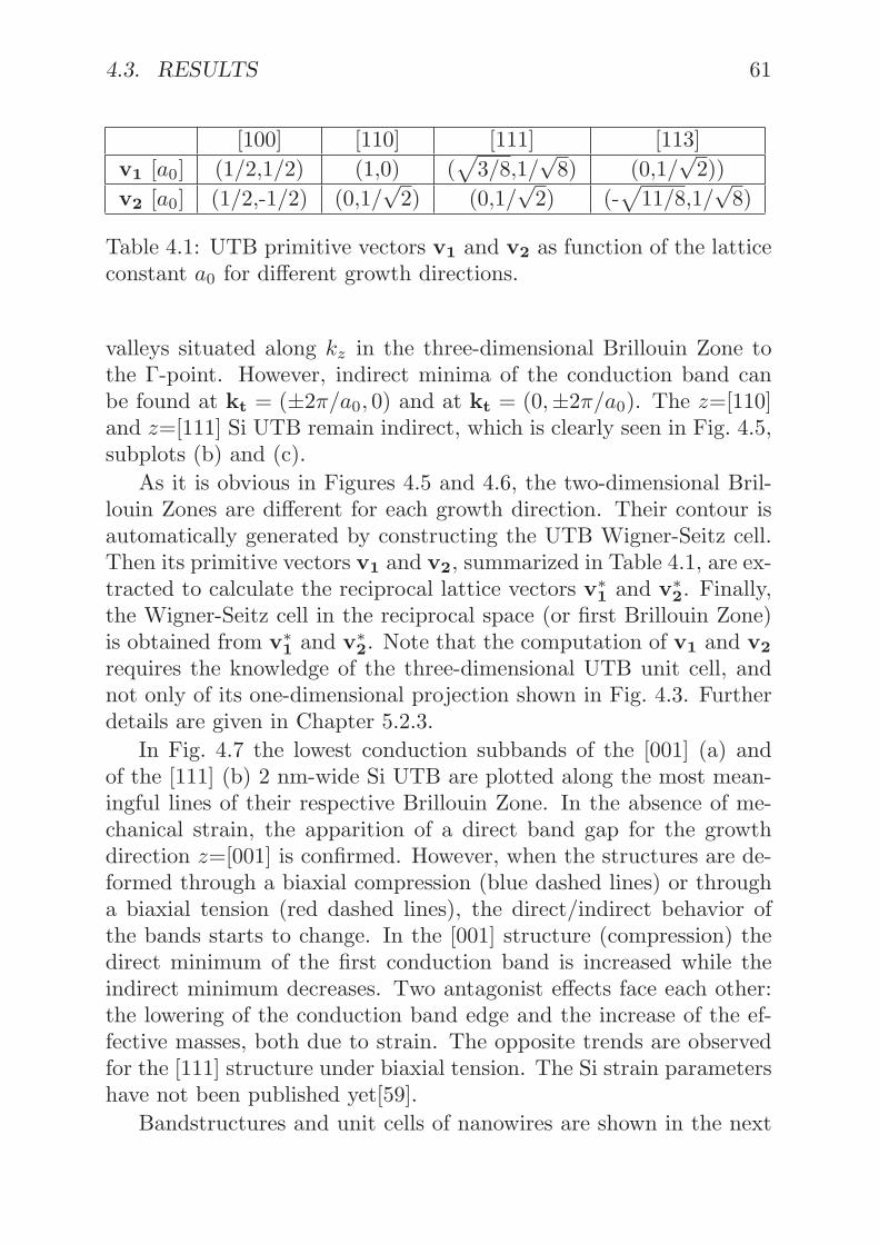
4.3. RESULTS 61
[100] [110] [111] [113]v1 [a0] (1/2,1/2) (1,0) (
√3/8,1/
√8) (0,1/
√2))
v2 [a0] (1/2,-1/2) (0,1/√
2) (0,1/√
2) (-√
11/8,1/√
8)
Table 4.1: UTB primitive vectors v1 and v2 as function of the latticeconstant a0 for different growth directions.
valleys situated along kz in the three-dimensional Brillouin Zone tothe Γ-point. However, indirect minima of the conduction band canbe found at kt = (±2π/a0, 0) and at kt = (0,±2π/a0). The z=[110]and z=[111] Si UTB remain indirect, which is clearly seen in Fig. 4.5,subplots (b) and (c).
As it is obvious in Figures 4.5 and 4.6, the two-dimensional Bril-louin Zones are different for each growth direction. Their contour isautomatically generated by constructing the UTB Wigner-Seitz cell.Then its primitive vectors v1 and v2, summarized in Table 4.1, are ex-tracted to calculate the reciprocal lattice vectors v∗
1 and v∗2. Finally,
the Wigner-Seitz cell in the reciprocal space (or first Brillouin Zone)is obtained from v∗
1 and v∗2. Note that the computation of v1 and v2
requires the knowledge of the three-dimensional UTB unit cell, andnot only of its one-dimensional projection shown in Fig. 4.3. Furtherdetails are given in Chapter 5.2.3.
In Fig. 4.7 the lowest conduction subbands of the [001] (a) andof the [111] (b) 2 nm-wide Si UTB are plotted along the most mean-ingful lines of their respective Brillouin Zone. In the absence of me-chanical strain, the apparition of a direct band gap for the growthdirection z=[001] is confirmed. However, when the structures are de-formed through a biaxial compression (blue dashed lines) or througha biaxial tension (red dashed lines), the direct/indirect behavior ofthe bands starts to change. In the [001] structure (compression) thedirect minimum of the first conduction band is increased while theindirect minimum decreases. Two antagonist effects face each other:the lowering of the conduction band edge and the increase of the ef-fective masses, both due to strain. The opposite trends are observedfor the [111] structure under biaxial tension. The Si strain parametershave not been published yet[59].
Bandstructures and unit cells of nanowires are shown in the next

62 CHAPTER 4. BANDSTRUCTURE MODEL
(a)
kx [1/a
0]
k y [1/
a 0]
kx [1/a
0]
k y [1/
a 0]
(b)
k y [1/
a 0]
(c)
kx [1/a
0]
(d)
−2π 2π
2π
2π
2π
−2π
2π
2π
2π
2π
kx [1/a
0]
k y [1/
a 0]
−2π −2π
Figure 4.5: Lowest conduction band contour of 2 nm-wide ultra-thinbodies plotted within their first two-dimensional Brillouin Zone. Thegrowth direction z is (a) [001], (b) [110], (c) [111], and (d) [113]. TheUTB in subplots (a), (b), and (c) are made out of Si, the UTB in (d)is made out of GaAs. Blue represents low energies, red high energies.
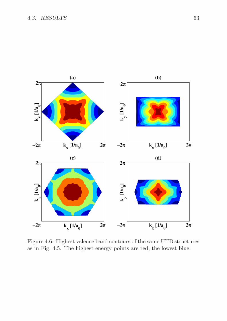
4.3. RESULTS 63
(a)
kx [1/a
0]
k y [1/
a 0]
(b)
kx [1/a
0]
k y [1/
a 0]
(c)
kx [1/a
0]
k y [1/
a 0]
(d)
kx [1/a
0]
k y [1/
a 0]
−2π 2π
2π
2π
2π
−2π
2π
2π
2π
2π
−2π −2π
Figure 4.6: Highest valence band contours of the same UTB structuresas in Fig. 4.5. The highest energy points are red, the lowest blue.

64 CHAPTER 4. BANDSTRUCTURE MODEL
−4 −2 0 2 4 61
1.5
2
2.5
3
3.5(a)
k [1/a0]
E [
eV]
no straincompression
−4 −2 0 2 4 61
1.5
2
2.5
3
3.5(b)
k [1/a0]
E [
eV]
no straintension
[110] [100] [31/210] [100]
Figure 4.7: Lowest conduction subbands for (a) the [001] and for(b) the [111], 2 nm-wide, Si UTB, along different lines in the BrillouinZone. The black lines have no strain, the blue dashed lines are exposedto a biaxial compression (εxx=εyy=-0.02, εzz=0.0155), the red dashedlines to a biaxial tension (εxx=εyy=0.02, εzz=-0.0089).
Chapter, where they are used to verify the transport properties ofidealized two-dimensionally confined structures. Applications of theUTB and nanowire bandstructure calculations can be found in Ref. [60].
4.4 Summary
In this Chapter the semi-empirical tight-binding method was pre-sented and applied to the calculation of bulk, ultra-thin body, andnanowire bandstructures. The code that was developed in this frame-work builds the core of an interactive tool called Bandstructure Labthat is available online[61]. All the features described in this Chapterare included in the online version.

Chapter 5
Transport Model
5.1 Introduction
In this Chapter, the sp3d5s∗ bandstructure model is incorporatedinto a three-dimensional quantum transport simulator. The goal isto simulate nanowire transistors. Non-equilibrium Green’s function(NEGF)[62, 63] or Wave Function[64] formalisms are well suited forthat purpose, but both approaches suffer from the computational bur-den caused by the open boundary conditions (OBCs) calculation. Inmost of the simulations, nanowires can be separated into a transportdirection (the x-axis, for example) and into two transverse directions(y and z). In these cases, the wire unit cell in the transport directionis a slab composed of different atomic layers (planes orthogonal to thetransport direction). The number of atomic layers that make up therepeatable wire slab depends on the crystal orientation.
In the ideal case, each unit cell has N atoms. It is connected tothe previous and to the next slab. The sp3d5s∗ tight-binding methodincludes ten orbitals without spin-orbit coupling and twenty with cou-pling, and the size of the block matrices involved in the calculationof the OBCs is either 10N or 20N . Iterative algorithms[44] requirethe inversion of very dense or even full matrices of this size untilconvergence is achieved, typically after 20 to 40 steps. In scatteringboundary methods (SBM)[65], the reservoir state eigenfunctions are
65

66 CHAPTER 5. TRANSPORT MODEL
calculated by solving a generalized eigenvalue problem (GEVP) of size20N (without spin) or 40N (with spin). Obviously, if the wire crosssection increases, or, if a special crystal orientation is chosen so thata wire slab contains many atoms, the efficiency of the iterative andthe SBM with GEVP degrades and a high amount of the CPU timeis dedicated to the boundary condition calculation.
A new approach to treat the OBCs problem is investigated. Start-ing from a scattering boundary ansatz, one takes advantage of theatomic fitting in the nanowires and adapts the physical descriptionof a slab. This method works not only for the usual [100] transportdirection and square cross section[62, 63, 64, 65], but for any crystalorientation such as [110], [111], or [113], and any wire shape (e. g. tri-angular, circular, T, hexagonal, ...). Furthermore, the computationalburden increases proportionally to the cross section dimensions, as inthe iterative and the GEVP approaches (staying nevertheless lowerthan in both cases), but not as function of the crystal orientation. Ahigher number of atomic layers (and therefore more atoms) in a slabwith the same size does not necessarily lead to more effort to com-pute the OBCs as it happens with other methods. The results canthen be coupled to a NEGF (if incoherent scattering are included) orto a Wave Function solver (much more efficient in the ballistic case).Wires with non-ideal reservoirs (for example quantum well reservoirs)are also considered. It is shown that the new method works for anyinput electrostatic potential, for which no self-consistent adjustmenthas been performed (Chapter 6).
The Chapter is organized as follows: in Section 5.2, a new methodis described to calculate the open boundary conditions for quantumtransport in nanowires, the improvement compared to previous treat-ments is highlighted, and the coupling to different solution schemes isderived. An additional simplification based on the device symmetry isdescribed. Section 5.3 presents results for Si, GaAs, and unstructuredAlGaAs wires with different cross sections and crystal orientationsand it examines the influence of applied bias, of biaxial strain and ofthe contacts. The transmission coefficients as well as the density ofstates are calculated for these different configurations. In Section 5.4,the numerical implementation, the advantages and disadvantages of aWave Function and of a NEGF device calculation, and the differentalternatives for the open boundary conditions are discussed.

5.2. THEORY 67
5.2 Theory
In this Section, a new computational procedure to obtain open bound-ary conditions in a two-dimensionally confined quantum transportproblem and the coupling to a NEGF and a Wave Function ballisticsolver are described. It is based on a scattering-boundary approach.Figure 5.1 shows the schematic view of a nanowire with wire lengthLw (scattering boundary region) without semi-infinite reservoirs. Ef-fective transport occurs along the x-axis while y and z are directionsof confinement. Each atom is characterized by a set of orbitals. In thesp3d5s∗ tight-binding method, ten different orbitals are kept. Each ofthem is twofold degenerate, if spin orbit coupling is considered.
x
y
Lw
z
Figure 5.1: Schematic view of an atomistic nanowire. x is the trans-port axis, y and z are confinement directions, Lw represents the wirelength. Each atom is considered as well as the connections to its fournearest neighbors, except at the surface.
Independent of the underlying formalism, the Schrodinger equa-tion is explicitly or implicitly solved with proper boundary conditions.An incident electron, coming from the left or the right reservoir, withenergy E measured relative to the top of the valence band, can bescattered into reflected states that propagate back to their origin orinto transmitted states that propagate to the other contact(s). The

68 CHAPTER 5. TRANSPORT MODEL
device equation can be written as
H|ψE〉 = E|ψE〉. (5.1)
The Hamiltonian H contains the lattice and the electrostatic poten-tials. The scattering wave function |ψE〉 can be expanded in termsof orthogonalized Lowdin atomic orbitals φσ(r) of type σ (s, p, d, orexcited s∗)
ψ(r;E) =∑
σ,i,j,k
Cσijk(E)φσ(r−Rijk)
|ψE〉 =∑
σ,i,j,k
Cσijk(E)|ijk, σ〉, (5.2)
where Cσijk(E) is the expansion coefficient for the orbital σ of an atom
situated at R = (xi, yj , zk) in the nanowire. To solve Eq. (5.1), oneworks in a slab basis[66]. A slab represents the minimal number ofatomic layers required to generate an infinite nanowire, if it is trans-lated in the transport direction (for example, a slab is composed offour atomic layers if x is aligned with [100] and six layers for [111]).A slab has a width ∆. A nanowire with length Lw is therefore com-posed of Lw/∆ cells that represent its central scattering region. Inthis basis, the scalar Cσ
ijk(E) becomes a vector Ci(Rs, E), where i de-
notes the ith wire slab and Rs the position and the orbital type of anatom localized inside of it. Considering only connections to the nearestneighbors, disregarding three-center integrals[32], and left-multiplyingEq. (5.1) with 〈ijk, σ| at each position and for each orbital, the matrixequations
(E −Hii)Ci(Rs, E) −Hii+1Ci+1(Rs, E) −Hii−1Ci−1(Rs, E) = 0(5.3)
or
DiiCi(Rs, E) + Tii+1Ci+1(Rs, E) + Tii−1Ci−1(Rs, E) = 0(5.4)
are obtained, whose elements E − Hii ≡ Dii describes the on-siteenergy and the bond connections within a slab i, Hii+1 ≡ −Tii+1 is
5.2. THEORY 69
the coupling to the next slab, and Hii−1 ≡ −Tii−1 is the coupling tothe previous one. If tb is the tight-binding order (10 without spin,20 with) and each slab contains N atoms, the size of these squarematrices is tbN . Equation (5.4) is valid in the device as well as inthe semi-infinite left and right contacts, where a scattering boundaryansatz is applied to find the coefficients Ci(Rs, E) (i denotes a slabin the left lead). For brevity, only the left contact is treated, thederivation for the other(s) is obvious
Ci(Rs, E) =1√Nx
∑n
(ane
ikn(E)xiϕ+i,n(Rs, E)+
bne−ikn(E)xiϕ−
i,n(Rs, E)). (5.5)
Here, Nx is a normalization constant, an is the injection coefficientfor a state ϕ+
i,n(Rs, E) transmitted through the device (i.e. flowingfrom left to right), and bn is the coefficient for a state ϕ−
i,n(Rs, E) re-flected back in the contact, respectively. ϕ±
i,n(Rs, E) (associated with
e±ikn(E)xi) is the nth reservoir state and can be either propagating orexponentially decaying. Inserting Eq. (5.5) into Eq. (5.4) and separat-ing the transmitted and the reflected part of the coefficient Ci(Rs, E),the fact that both resulting contributions must vanish for each quanti-zation level n is exploited. In effect, the contacts are assumed infiniteand(
Dii + Tii+1e±ikn(E)∆ + Tii−1e
∓ikn(E)∆)ϕ±i,n(Rs, E) = 0, (5.6)
with the slab width ∆. Only one of these two equations needs tobe solved because the solution of the other equation is automaticallytaken into account[67]. It is worth noting that Eq. (5.6) is exactly theequation solved for the bandstructure calculation of an infinite wire,but with exchanged input and output variables. In the open bound-ary conditions problem, one searches for all the wave vectors k corre-sponding to one injection energy E. In the bandstructure case, onecalculates the energy eigenvalues at one k point. To recognize if thecalculated state is transmitted or reflected, two different approachesare required. For a propagating state (i.e., kn(E) has no imaginarypart), the energy E(kn) is derived with respect to kn because the

70 CHAPTER 5. TRANSPORT MODEL
particle velocity vn ∝ dE(kn)/dkn is related to this quantity. In theleft reservoir, a positive vn means transmission, a negative reflection.For an exponentially decaying state, the imaginary part of k indicatesthe state nature. A positive imaginary part, or |exp(ikn(E)∆)| < 1,denotes a decaying transmission, while |exp(−ikn(E)∆)| < 1 corre-sponds to a decaying reflection. These operations are done after thekn(E) and ϕi,n(Rs, E) are calculated at one given injection energy E.
A well established procedure consists in transforming Eq. (5.6) tothe following complex non-hermitian (with spin-orbit coupling) or realnon-symmetric (without) generalized eigenvalue problem (GEVP)[64,65] of size 2tbN(Dii Tii+1
1 0
)·(
ϕiϕi+1
)= eik∆
( −Tii−1 00 1
)·(
ϕiϕi+1
),
(5.7)
where the variables E and Rs are omitted for brevity. Despite the factthat the numerical solution of Eq. (5.7) avoids matrix inversion[68],it is still computationally intensive to obtain the desired k and ϕvalues for a nanowire with a large cross section or a crystal orientationdifferent from [100]. However, going back to Eq. (5.6), a better insightinto the physical structure of the matrices Dii, Tii+1, and Tii−1 leadsto a simplified procedure to evaluate the OBCs. For the derivation, atransport axis in the [100] direction is used (the method is not limitedto this specific orientation). In this case, a slab i in the left (right)reservoir is composed of four atomic layers, two entangled pairs ofcations and anions. A cation (anion) layer is only connected to theprevious and to the next anion (cation) layers. Therefore, Eq. (5.6)can be written in an atomic layer basis instead of a slab basis
D00ϕ0 + T0−1ϕ−1 + T01ϕ1 = 0D11ϕ1 + T10ϕ0 + T12ϕ2 = 0D22ϕ2 + T21ϕ1 + T23ϕ3 = 0D33ϕ3 + T32ϕ2 + T34ϕ4 = 0 .
(5.8)
In the layer basis, Dii describes the one-site energy as well as theconnections to the neighbor atoms inside layer i, Tii±1 the couplingto the next and to the previous layers, ϕi is the eigenfunction of

5.2. THEORY 71
layer i and the total vector ϕ = [ϕ0; ϕ1; ϕ2; ϕ3] is the same as inEq. (5.6). With the scattering boundary ansatz from Eq. (5.5) andthe assumption that all reservoir slabs are identical, one obtains ϕ−1 =ϕ3×exp(−ik∆), ϕ4 = ϕ0×exp(ik∆), and T34 = T−10 so that Eq. (5.8)becomes
D00 T01 0 T0−1e
−ik∆
T10 D11 T12 00 T21 D22 T23
T−10eik∆ 0 T32 D33
·
ϕ0
ϕ1
ϕ2
ϕ3
= 0. (5.9)
One defines two new variables H and P as
H =
D00 T01 0 0T10 D11 T12 00 T21 D22 T23
T−10 0 0 0
, (5.10)
P = −
0 0 0 T0−1
0 0 0 00 0 0 00 0 T32 D33
, (5.11)
respectively, and use them to rewrite Eq. (5.9)
Hϕ = e−ik∆Pϕ. (5.12)
Equation (5.12) looks almost like an eigenvalue problem, but for thatpurpose the matrix H or P should be inverted so that on one sideof the equation, there were a matrix M and on the other an eigen-value exp(−ik∆). This is not possible because P obviously cannot beinverted due to its structure. In addition, H is also singular as theconnecting block T23 contains columns filled exclusively with zeros(nearest neighbor approximation). A slight modification of Eq. (5.12)can remove this deficiency and generate a normal eigenvalue problem(EVP)
Hϕ = e−ik∆Pϕ+ Pϕ− Pϕ(H−P)ϕ =
(e−ik∆ − 1
)Pϕ(H−P)−1 Pϕ = 1
e−ik∆−1ϕ
Mϕ = λϕ.
(5.13)

72 CHAPTER 5. TRANSPORT MODEL
The matrix (H−P) can always be inverted, except for E = E(k = 0)which is one of its eigenvalues. To calculate the bandstructure atk = 0 for an infinite wire whose slabs are described by Eq. (5.4),the eigenvalues of a matrix identical to (H−P) have to be found.However, by adding a small imaginary part to the energy E or byartificially avoiding E = E(k = 0), the matrix M is always definedand has an advantageous structure
M =
0 0 M02 M03
0 0 M12 M13
0 0 M22 M23
0 0 M32 M33
. (5.14)
It is thus not necessary to consider the whole matrix M in the eigen-value problem defined in Eq. (5.13), but only its lower right cornerand (
M22 M23
M32 M33
)·(ϕ2
ϕ3
)=
1e−ik∆ − 1
(ϕ2
ϕ3
). (5.15)
When the transport direction is aligned with the [100] crystal axis,the complex non-hermitian (spin-coupling) or real non-symmetric (nospin) eigenvalue problem to be solved is of size tbN/2, which is asignificant improvement compared to Eq. (5.7) whose matrices havesize 2tbN . Apart from a gain of a factor 4 in the size of the blocks,it is not required to work with a GEVP, but with a normal EVP. Aweakness resides in the inversion of the matrix (H−P) with size tbN .This causes an additional computational effort, but the high sparsityof (H−P) enables a fast inversion so that the new method presentedhere is more efficient than what was published previously[64, 65] (seealso Table 5.2 for quantitative results).
Once the solution of Eq. (5.15) is obtained, the eigenfunctions ofthe first (ϕ0) and of the second (ϕ1) atomic layers are computed with(
ϕ0
ϕ1
)= − (e−ik∆ − 1
)( M02 M03
M12 M13
)·(ϕ2
ϕ3
). (5.16)
Note that the approach presented for a transport axis in the [100]direction works for all crystal orientations, as mentioned above, evenif one atomic layer is connected not only to the next layer but to

5.2. THEORY 73
several consecutive layers. In this case, the matrices H and P aregenerated in such a way that they minimize the bandwidth of thematrix M . The size of the eigenvalue problem becomes as small aspossible. An illustration of this principle will be given in Section5.3. Another possibility to reduce the size of M is to consider thesymmetry properties of the simulated nanowires.
Figure 5.2: Cross section of a rectangular GaAs wire with rotationalsymmetry properties around its center.
Figure 5.2 shows the cross section of a rectangular GaAs wirewhose transport direction is aligned with the [100] crystal axis. Infact, this cross section corresponds to the projection of a wire slabcontaining 41 atoms distributed over four atomic layers, two cation(blue atoms) and two of anion (red atoms) layers into one single atomicplane. By writing down Eq. (5.6), it is obvious that the cross sectionof Fig. 5.2 has symmetry properties. For example, the atoms in thedomain limited by the dashed line can be rotated by 180o aroundthe wire center. One could think that the cross section has also avertical, a horizontal, or a diagonal symmetry axis, but this is nottrue since the reflected atoms would not belong to the same atomicplane as the atoms they replace. Therefore, Eq. (5.15) has to be

74 CHAPTER 5. TRANSPORT MODEL
solved two times, but with a size divided by two, once for symmetricand once for antisymmetric rotation. The computational burden issignificantly reduced, even more if the two cases are treated on parallelCPUs. This simplification works for the semi-infinite contacts, if theelectrostatic potential applied to them has the same symmetry asthe atom positions, which is the case for double-gate or all-around-gate nanowire transistors. If the transport direction is aligned witha different crystal orientation, the symmetry properties are differentand must be studied case by case.
5.2.1 Wave Function Solver
In the Wave Function formalism, one needs to couple the OBCs fromEqs. (5.15) and (5.16) to the Schrodinger equation expressed in aslab basis. It is assumed that the considered nanowire has Ns slabsstarting from 1 to Ns, and that the injected electrons come from theleft contact (slab 0)
L00 L01
L10 D11 T12
T21 D22 T23
. . . . . . . . .TNsNs−1 DNsNs
RNsNs+1
RNs+1NsRNs+1Ns+1
×
C0
C1
C2
...CNs
CNs+1
=
I0I10...00
. (5.17)
To calculate the elements L00, L01, L10, (coupling to the left reservoir)RNs+1Ns+1, RNsNs+1, RNs+1Ns
, (coupling to the right reservoir), I0,and I1 (injection mechanism), the lead eigenfunctions ϕi,n(Rs, E) andwave vectors kn(E) are classified as function of their properties. TheN+
p states propagating from the left to the right (transmitted) arecast into the (tbN) ×N+
p matrix ϕ+p , the N+ transmitted states into

5.2. THEORY 75
ϕ+ (size (tbN)×N+), and finally the N− reflected states into ϕ− (size(tbN) × N−). The same notation is applied to kn(E). Furthermore,exp(ik±∆) is a diagonal matrix containing the contributions from allthe transmitted (+) or reflected wave vectors (-) with k+ = −k−.One obtains
L00 = ϕ+†D00ϕ
− + ϕ+†T10ϕ−e−ik−∆
L01 = ϕ+†T01, L10 = T10ϕ−
I0 = −(ϕ+†D00ϕ
+p + ϕ+†T10ϕ
+p e
−ik+p ∆)Ainj(E)
I1 = −T10ϕ+pAinj(E) .
(5.18)
The definition of the matrices RNs+1Ns+1, RNsNs+1, and RNs+1Ns
follows Eq. (5.18). If the states are injected from the right contact,the right-hand side of Eq. (5.17) would have two non-zero vectors INs
and INs+1. The diagonal matrix Ainj is defined so that the elementsA†inj×Ainj represent the probability that a state injected from the left
with energy E is occupied. Equation (5.17) must be solved for each in-jection energy and for each right-hand side containing all propagatingstates from the different device contacts. Consequently, the unknownCi coefficients depend on the energy E (or wave vector k(E)), on theport and on the state they come from (index p and n, respectively)for all i, plus on the orbital type σ, and on the atom position Rs
in the slab i if 1 ≤ i ≤ Ns. They are labeled Cσi,p,n(Rs, k(E)) for
1 ≤ i ≤ Ns and Ci,p,n(k(E)) else. The carrier density in the nanowiren(r) is given by
n(r) = 〈r|ψ〉〈ψ|r〉n(x, r) =
1Nx
∑n,p,σ
∑i,Rs
∑k
|Cσi,p,n(Rs, k)|2f(Ep,n(k) − µp)
×δ(x− xi)δ(r −Rs)
=∆2π
∑n,p,σ
∑i,Rs
π/∆∫0
dk |Cσi,p,n(Rs, k)|2f(Ep,n(k) − µp)
×δ(x− xi)δ(r −Rs). (5.19)
In the contacts, Fermi distributions with a chemical potential µp areassumed. The injection energy (from port p) of a state n with wave

76 CHAPTER 5. TRANSPORT MODEL
vector k is Ep,n(k). The product of two orbital functions φσ intro-duced in Eq. (5.2) should be present in Eq. (5.19). It is replaced byδ(x−xi)δ(r−Rs) because the resulting term is very localized aroundone atom situated at (xi, Rs). Finally, the sum over the wave vector kis converted to an integral. In this formalism, the position-dependentdensity of states Zp(x, r, E) injected from port p is defined as
Zp(x, r, E) =∆2π
∑n,σ
∑i,Rs
π/∆∫0
dk |Cσi,p,n(Rs, k)|2δ(E − Ep,n(k))
×δ(x− xi)δ(r −Rs). (5.20)
The current density is calculated by using the two-terminal Landauerformula for the non-interacting case[69]. It requires the knowledge ofthe transmission coefficient T (E) weighted with the contact distribu-tion functions. If an electron is injected from the left port p = 1, T (E)at the right contact is calculated with CNs+1 (situation described inEq. (5.17))
T (E) =∑n,m
|CNs+1,p=1,n(km)|2∣∣∣∣ dEdkm
∣∣∣∣∣∣∣∣ dEdkn
∣∣∣∣−1
. (5.21)
The indices n and m run over all the propagating states in the left(slab 0) and the right (slab Ns + 1) reservoirs, respectively, not overthe exponentially decaying states.
Equation (5.21) requires the knowledge of the derivative of theenergy E with respect to the wave vector k. dE(k)/dk is obtained byderiving Eq. (5.6)
dEdk
� −2Im(ϕ+†i,k(Rs, E)Tii+1ϕ
+i,k(Rs, E)eik∆
). (5.22)
The terms containing dϕ±i,k/dk are neglected because they are much
smaller than the contribution kept in Eq. (5.22).
5.2.2 NEGF Solver
Recently, the Non-Equilibrium Green’s Function (NEGF) formalismhas become very popular for the simulation of quantum transport in

5.2. THEORY 77
nanodevices. In the following, it is shows that the scattering OBCsobtained above can be used to calculate the retarded boundary self-energies ΣRB of the NEGF formalism. The use of iterative solvers[44]for the OBCs calculation (20 to 40 inversions of a very dense or fullmatrix of size tbN) is less efficient than the approach proposed inthis Chapter (one inversion of a sparse tbN matrix and solution ofan eigenvalue problem with reduced size). However, ΣRB is obtainedafter some simple steps, and not as the direct output of an iterativesolver. The starting point is the calculation of the contact retardedGreen’s function gRij(Rs1Rs2, E)[14] (i and j are slab indices, Rs1 andRs2 are the atom positions inside the slabs, E refers to the energy,Rs1, Rs2, and E are neglected in the remainder of this Section). Theequation for the left reservoir is derived, assuming that slab 0 is thelast slab before the device and T01 = 0. This is the condition for thecalculation of gRij . According to Eqs. (2.57) and (2.58) the followingsystem of equations must be solved[70]{
D00gR00 + T0−1g
R−10 = I
D−1−1gR−10 + T−10g
R00 + T−1−2g
R−20 = 0. (5.23)
With the invariance of the slabs in the reservoirs, D−1−1 = D00 andT−1−2 = T0−1. It is easy to prove that the following ansatz for gRij(assuming the same notation conventions as in the Wave Functioncase)
gRij = ϕ−0 e
ik−xi gRe−ik−xjϕ−†0 (5.24)
satisfies the second part of Eq. (5.23) and that it can be inserted intothe first part to calculate gR and then ΣRB
11 . After some straightfor-ward algebra, it is found that{
gR =(ϕ−†
0 D00ϕ−0 + ϕ−†
0 T0−1ϕ−0 e
−ik−∆x
)−1
ΣRB11 = T10g
R00T01 = T10ϕ
−0 g
Rϕ−†0 T01.
(5.25)
The boundary self-energy ΣRBNsNs
of the right contact is obtained witha similar procedure. The carrier and the current density are calcu-lated with a recursive algorithm[23] involving the Hamiltonian H. Itcorresponds to the left-hand side matrix of Eq. (5.17) without theboundary condition terms Lij and Rij removed and replaced by theboundary self-energies ΣRB
11 and ΣRBNsNs
.

78 CHAPTER 5. TRANSPORT MODEL
2DEGWELL 2DEG
WELL
1DEG WIRE
1DEG WIRE
v1
v1
v2
v2
x x
y y
BZ BZ
Figure 5.3: Projection of the quantum well reservoir unit cell (redatoms) and its 8 nearest-neighbor unit cells (blue atoms) onto the(x, y) plane with the displacement vectors v1 and v2. The growthdirection z is aligned with [001] and the transport direction in the wirex with [100]. Left: primitive QW unit cell (4 projected atoms). Right:new QW unit cell with v1 and v2 aligned with x and y (8 projectedatoms). Both insets show the corresponding two-dimensional BrillouinZone drawn in a cut plane of the three-dimensional one at kz=0.
5.2.3 Quantum Well Reservoir
As the metallic contacts (Ti for example) of nanowire transistors areoften much wider than the device itself, they should be modeled asquantum well (QW) reservoirs with charge confinement in one direc-tion only. As a first approximation, the contacts are made of thesame semiconducting material as the nanowire. It is then possible tostudy the transition from a two-dimensional electron gas (2DEG) inthe QW reservoirs to a one-dimensional electron gas (1DEG) in thewire channel[71].
To calculate the open boundary conditions in the Well-Wire con-figuration, Fig. 5.3 is considered. In the nanowire (labeled 1DEG),the electrons are free only in their transport direction x, but are con-fined in the y and z (in-plane axis) directions. In the QW reservoirs(labeled 2DEG, only left reservoir visible), the electrons can freelymove along x and y, but are confined in the z direction.
In the previous Section, it was demonstrated that, at a given en-ergy E, states ϕn(E) are injected from the reservoirs into the device

5.2. THEORY 79
for all the authorized wave vectors kxn(E) aligned with the wire trans-port direction x. QW reservoirs add a third variable ky related topossible displacements in the y direction in the 2DEG. Instead of de-pending on the injection energy E only, the reservoir states ϕn(E, ky)and wave vectors knx(E, ky) are also calculated for all the possible kyin the first two-dimensional QW Brillouin Zone.
To compute kx(E, ky) and ϕn(E, ky) in the QW reservoirs, the QWunit cell must be determined. In Fig. 5.3, on the left, the primitiveunit cell (red atoms, projected onto the (x, y) plane) of a structurewith x=(100), y=(010), and z=(001) is shown. By translating it withthe vectors v1 and v2, the semi-infinite QW reservoirs can be totallyconstructed. Although this unit cell is the smallest one, it is notwell suited to be coupled to a nanowire. Since the device transportdirection is x, it is advantageous to have v1 or v2 aligned with it andthe other vector aligned with y. For that purpose, a larger unit cellsatisfying this condition is constructed in the right part of Fig. 5.3(red atoms). Note that the size of the corresponding two-dimensionalBZ is divided by two and the QW bandstructure is folded.
T 01ii−1 D01
ii T 01ii+1
T 00ii−1 D00
ii T 00ii+1
T 0−1ii−1 D0−1
ii T 0−1ii+1
Table 5.1: Numerical transposition of the right side of Fig. 5.3.
The ϕn(E, ky)’s are then the eigenstates of the unit cell shown inthe right part of Fig. 5.3 and comprising NA atoms. They are vectorsof size N = NA× tb and should be written as ϕi,j,n(E, ky) if the spacedependence is taken into account (i and j indicate the position of theunit cell along the x and y axis, respectively). To calculate them, theDii, Tii±1, and Tii−1 are replaced in Eq. (5.6) by
Dii → D00ii +D01
ii eiky∆y +D0−1
ii e−iky∆y (5.26)Tii±1 → T 00
ii±1 + T 01ii±1e
iky∆y + T 0−1ii±1e
−iky∆y (5.27)
and ∆ becomes ∆x, the width of the unit cell in the x direction (∆y
is its width along y). A look at the right side of Fig. 5.3 and at

80 CHAPTER 5. TRANSPORT MODEL
its numerical transposition in Table 5.1 can help understanding themeaning of all the terms in Eqs. (5.26) and (5.27). The QW unitcell, depicted by the red atoms and characterized by D00
ii has eightneighbor cells (blue atoms). The connections of the central unit cell(red) to the others is given by the remaining blue terms in Table5.1. The modified Eq. (5.6), expressed in a “unit cell” basis can thenbe rewritten in an atomic layer basis, as in Eq. (5.8). Finally, theϕn(E, ky)’s are calculated according to Eqs. (5.9) to (5.16).
The coupled QW-Wire system is solved in the NEGF formalism.The nanowire boundary self-energy ΣRB is obtained with the helpof the contact retarded Green’s function gRi1i2j1j2(z1z2, E) (i1 and i2are unit cell indices along x, j1 and j2 along y, z1 and z2 are theatom positions within the unit cell, E refers to the energy). Onlythe left reservoir is considered, the derivation for the right one isstraightforward. First, the system of equations (5.23) is generalizedto the two-dimensional electron gas
∑j=0,±1
(D0j
00gR00j0 + T 0j
0−1gR−10j0
)= I∑
j=0,±1
(D0j
−1−1gR−10j0 + T 0j
−10gR00j0 + T 0j
−1−2gR−20j0
)= 0.
(5.28)
which can be solved with the following ansatz for gRi1i2j1j2
gRi1i2j1j2 =1Ny
∑ky
ϕ−00e
ik−xi1 gR(ky)e−ik−xi2ϕ−†00 e
iky(yj1−yj2 ). (5.29)
Ny is a normalization constant. Eq. (5.29) satisfies the second part ofEq. (5.28) and can be used in the first part to derive gR
gR(ky) = (ϕ−†00 (ky)
∑jy=0,±1
[D0j00ϕ
−00(ky) +
T 0j0−1ϕ
−00(ky)e
−ik−∆x ]eiky(jy∆y))−1. (5.30)
As shown in Fig. 5.3, the width ∆y of the quantum well unit cell canbe thinner than Ly, the width of the Wire cross section. Therefore,the total contact Green’s function gR00 must be generated from the

5.3. RESULTS 81
various gR00j1j2 . If it is assumed that Ly = N∆y, one finds that
gR00 =
gR0011 gR0012 · · · gR001NgR0021 gR0022 · · · gR002N
......
. . ....
gR00N1 gR00N2 · · · gR00NN
(5.31)
and
ΣRB11 = T10g
R00T01, (5.32)
which is similar to Eq. (5.25). Carrier and current density are solvedwith a recursive algorithm[23]. A Wave Function approach of theQW-Wire problem is more complicated due to the multiplication ofthe states that should be injected into the device. The left-handside of Eq. (5.17) becomes very large, leading to an increase of thecomputational burden.
5.3 Results
5.3.1 Ideal Contacts
In this Section, simulations of Si and GaAs nanowires with differ-ent cross sections and crystal orientations (see Fig. 5.4), but withalmost the same length Lw=22.5±0.5 nm (given in Table 5.2) arepresented. The contacts are assumed ideal (semi-infinite prolongationof the nanowire). Lw is the central scattering region of the device.According to Fig. 5.1, x is the transport direction, y and z are direc-tions of confinement and delimit the device cross section. The sp3d5s∗
tight-binding parameters were optimized by T. B. Boykin et al. toreproduce Si[34] and GaAs[53] bulk bandstructures. Figure 5.4 de-picts different wire cross sections projected onto one atomic plane.They correspond to wire slabs, as introduced in Section 5.2, that arecomposed of the minimal number of atomic layers (all the atoms con-tained in a plane orthogonal to the x-axis). An infinite ideal wire isgenerated by translating a slab in the x-direction.
In Fig. 5.5, the electron bandstructure of infinite wires (calculatedwithout spin-orbit coupling) with the same cross sections as in Fig. 5.4

82 CHAPTER 5. TRANSPORT MODEL
(a) (d)
(b) (e)
(c) (f)
Figure 5.4: Cross sections of the different nanowires simulated in thisChapter (data in Table 5.2): (a) [100] Si rectangular wire, (b) [111] Sitriangular wire, (c) [100] Si circular wire, (d) [100] GaAs T-shape wire,(e) [110] GaAs hexagonal wire, and (f) [113] GaAs rectangular wire(blue: Ga, red: As). The cross section corresponds to the projectionof a wire slab on a single atomic plane.

5.3. RESULTS 83
is presented. Half of the one-dimensional Brillouin zone is drawn dueto symmetry with respect to k=0. The wave vectors are normalizedwith their maximum value kmax = π/∆, where ∆ is the length of awire slab in the transport direction.
Figure 5.6 shows the electron transmission of the same nanowiresas in Figs. 5.4 and 5.5 for three different operating conditions. Theopen boundary conditions (OBCs) are calculated with the eigenvaluemethod proposed in this paper. They are then coupled to a WaveFunction solver as described in Section 5.2.1. Spin-orbit coupling isneglected, because one considers electron transmission only and theeffects are small for the conduction band as it will be shows later inthis Section.
The unbiased device transmission coefficients T (E) in Fig. 5.6(blue lines) corresponds to the bandstructure of infinite structures.In effect, the semi-infinite left and right reservoirs as well as the cen-tral channel they are connected to form an uniform nanowire whoseelectrical properties do not vary in transport direction. In this case,if there are n available incident modes at energy E (i.e. modes with apositive velocity in the left reservoir and a negative in the right reser-voir), one has T (E) = n. This is a good way to check if the resultsobtained with the procedure outlined in Section 5.2 are correct.
When a linear bias of 0.1 V (green lines) or 0.2 V (red lines) isapplied to the nanowires, the band bending starts 5 nm after the leftcontact and ends 5 nm before the right contact. T (E) can no morebe related to the bandstructure of infinite wires, where the potentialdoes not vary from the left to the right semi-infinite leads. However,in order for transmission to occur, an incident mode must have thesame symmetry properties as the reservoir state that collects it onthe other side of the device. For example, a mode whose probabilitydensity has one single maximum in the middle of the cross section(caused by the confinement) is injected from the left reservoir. Onlystates with different probability densities are available in the rightreservoir. No transmission is possible at this energy because in theballistic regime, a state cannot change its symmetry during a passagethrough the channel. For energy E, if n modes are present in theleft reservoir and m in the right one, then T (E) ≤ min(n,m). Thisprinciple is illustrated in Fig. 5.6.
The six examples depicted in Fig. 5.4 are studied now. The first

84 CHAPTER 5. TRANSPORT MODEL
0 0.5 12.0
2.2
2.4
2.6
2.8
3.0(a)
k [norm.]
E [
eV]
0 0.5 12.2
2.4
2.6
2.8
3.0
3.2(b)
k [norm.]
E [
eV]
0 0.5 11.8
2.0
2.2
2.4
2.6
2.8(c)
k [norm.]
E [
eV]
0 0.5 12.2
2.4
2.6
2.8
3.0
3.2(d)
k [norm.]
E [
eV]
0 0.5 12.0
2.2
2.4
2.6
2.8
3.0(e)
k [norm.]
E [
eV]
0 0.5 12.4
2.6
2.8
3.0
3.2(f)
k [norm.]
E [
eV]
Figure 5.5: Conduction subbands of infinite (in the transport direc-tion) nanowires without an applied bias. The cross sections and thecrystal orientations are the same as in Fig. 5.4: (a) Si rectangularwire, (b) Si triangular wire, (c) Si circular wire, (d) GaAs T-shapewire, (e) GaAs hexagonal wire, and (f) GaAs rectangular wire.

5.3. RESULTS 85
2 2.5 30
2
4
6
8
10
(a)
E [eV]
TE
0.0 V0.1 V0.2 V
2.2 2.7 3.20
2
4
6
8
(b)
E [eV]
TE
0.0 V0.1 V0.2 V
1.8 2.2 2.60
2
4
6
8
10
(c)
E [eV]
TE
0.0 V0.1 V0.2 V
2.2 2.6 30
2
4
6
8
10
12
(d)
E [eV]
TE
0.0 V0.1 V0.2 V
2 2.3 2.60
5
10
15
20
(e)
E [eV]
TE
0.0 V0.1 V0.2 V
2.4 2.7 30
2
4
6
8(f)
E [eV]
TE
0.0 V0.1 V0.2 V
Figure 5.6: Electron transmission through the nanowires described inFig. 5.4 calculated without spin-orbit coupling and with a bias of 0.0V (blue lines), of 0.1 V (green lines), and of 0.2 V (red lines). Thelinear bias extends from 5 nm after the left contact to 5 nm beforethe right one, flat plateaus are left at both ends of the devices. (a) Sirectangular wire, (b) Si triangular wire, (c) Si circular wire, (d) GaAsT wire, (e) GaAs hexagonal wire, and (f) GaAs rectangular wire.

86 CHAPTER 5. TRANSPORT MODEL
structure (a) is a Si rectangular nanowire (1.2 nm × 1.2 nm) wherethe transport axis is aligned with [100], y with [010] and z with [001].A slab contains four atomic layers (width ∆=0.543 nm), 41 atoms,the wire 42 slabs, and therefore 1722 atoms. The square matrix Minvolved in the calculation of the OBCs has a size NM=410 but theeigenvalue problem in Eq. (5.15) has a reduced size of NEV P=210.This implies that 51.2% of NM is sufficient to calculate the k’s andthe ϕ’s. The remaining states (48.8%) have an infinite imaginary partand do not contribute to quantum transport.
From the bandstructure calculation in Fig. 5.5 (a), one can de-termine the unbiased transmission of Fig. 5.6. For example, the firstband (blue) starts at E=2.105 eV, and so does the transmission. Dueto the confinement effects, this conduction subband has a minimumat k=0 and [100]-oriented Si nanowires become direct band gap struc-tures with four of the six split valleys projected to k=0. At k=0, thethird band (cyan) turning on at E=2.176 eV is doubly degenerateand induces an increase of step-size 2 in the transmission T (E). Thefourth visible conduction band (magenta) has a minimum at k=0.25at E=2.444 eV. At this point, in the transmission plot, a doublestep is observed, because a state with positive velocity appears atk = 0.25 + δ, but also on the other side of the Brillouin Zone, atk = −0.25 + δ (with δ → 0). When one branch of this fourth bandstops at k = 0 at E=2.521 eV, the transmission encounters a stepdown (from 6 to 5) marking the turn-off of one channel. Following thisprocedure, the complete transmission can be explained in the unbi-ased case, proving that the results obtained in the quantum transportcalculation are correct.
When bias is applied to the device, a shift of 0.1 eV and 0.2 eV inthe transmission curves and a smoothing of the abrupt quantizationsteps at low energies are noticed. At high energy, in addition to theseeffects, the transmission changes its physical behavior: at E=2.89 eV(see arrow in Fig. 5.6 (a)), it would expected that T (E) with a biasof 0.2 V (red line) remains flat, but it actually goes down. This risesfrom the fact that all the bands with 2≤ n ≤9 are present in the leftreservoir (1 has just disappeared and 10 has not been reached yet) andall the bands with 1≤ m ≤6 are found in the right contact (first bandsituated at E=2.105 + 0.2 eV, band 7 has not started at E=2.788 +0.2 eV). Because of the symmetry properties of the probability density,

5.3. RESULTS 87
0 0.5 12
2.2
2.4
2.6
2.8
3Left Reservoir
k [normalized]
E [
eV]
−1 −0.5 02
2.2
2.4
2.6
2.8
3Right Reservoir
k [normalized]
E [
eV]
0 1 2 3 4 5 6 7Transmission
1 2 3 4 5 6 7Available Bands
Figure 5.7: Left and right reservoir bandstructures for the rectangularSi wire in Fig. 5.4 (a) with a bias of 0.2 V. The central subplotsshow the available bands for transmission through the device and thetransmission T (E).
only the following (n,m) couples are possible: (2,2), (3,3), (4,4), (5,5),and (6,6). Figure 5.7 shows the available bands in the left and theright reservoir at a given energy and confirms the explanation. Thusthe transmission at E=2.89 eV with a bias of 0.2 V must be smalleror equal to 5, as illustrated by the red line in Fig. 5.6 (a) and cannotremain on plateau number 6.
To verify that the results are correct when a bias is applied to thenanowires, a second simulation model is implemented; the OBCs arecalculated with an iterative method[44], cast into self-energies, andquantum transport is solved in the Non-equilibrium Green’s Function(NEGF) formalism[14, 23]. The comparison of the Wave Function(new eigenvalue method for the boundaries, blue and green lines) andof the NEGF (iterative OBCs, labeled “Sancho-Rubio”, red and yellowlines) solutions is shown in Figs. 5.8 and 5.9 for the Si rectangular wire(bias: 0.2 V). The electron transmission (Fig. 5.8) and the density ofstates in the first wire slab (Fig. 5.9) match perfectly, indicating thatthe new OBCs method introduced in this Chapter works under allconditions. In Fig. 5.9, there are two different densities of states, onecoming from the left contact (blue and red) and weighted by the leftelectron distribution function when carrier density is calculated, the

88 CHAPTER 5. TRANSPORT MODEL
2 2.1 2.2 2.3 2.4 2.5 2.6 2.7 2.8 2.9 30
1
2
3
4
5
6
7
E [eV]
Tra
nsm
issi
onnew methodSancho−Rubio
Figure 5.8: Electron transmission through the Si rectangular [100]-oriented wire in Fig. 5.4 for an applied bias of 0.2 V. The resultsobtained with the new OBCs method presented in this Chapter (blueline) are compared to the results from the iterative algorithm proposedby Sancho and Rubio[44] (red dashed line).
other (green and yellow) coming from the right contact and weightedby the right electron distribution function.
The second Si nanowire in Fig. 5.4 (b) has a triangular cross sec-tion (base: 1.6 nm, height: 1.2 nm), [111] as transport direction,[110] for y, and [112] for z. The six atomic layers composing a wireslab (∆=0.9405 nm) contain 60 atoms so that the matrixM has a sizeNM=600, but the OBCs eigenvalue problem has the order NEV P=160(26.7% of NM ). The wire is composed of 24 slabs or 144 atomic lay-ers. Its bandstructure is represented in Fig. 5.5 (b) for the infinite andunbiased case. No electron subbands appear in the energy range com-prised between 2.656 eV and 2.731 eV. Consequently, the transmissionmust vanish for these energies, as seen in Fig. 5.6 (b), even when a biasis applied to the device. The left reservoir keeps a constant potentialso that no transmission is possible between 2.656 eV and 2.731 eV.Furthermore, the potential of the right contact increases by 0.1 eV or0.2 eV leading to a second gap between 2.756 eV and 2.831 eV (bias:

5.3. RESULTS 89
2 2.1 2.2 2.3 2.4 2.5 2.6 2.7 2.8 2.9 310
0
101
102
E [eV]
Den
sity
of
Stat
es [
arb.
uni
ts]
Left: newLeft: SRRight: newRight: SR
Figure 5.9: Electron density of states (DOS) for the same wire andthe same conditions as in Fig. 5.8. The results obtained with the newmethod (solid lines) are compared to the results from the Sancho-Rubio iterative algorithm[44] (dashed lines): the contribution to thetotal DOS coming from the left contact (blue and red) and comingfrom the right contact (green and yellow) are shown in the first deviceslab (0≤ x ≤0.543 nm).
0.1 V) or 2.856 eV and 2.931 eV (bias: 0.2 V) where the transmissionalso disappears, in agreement with the simulation results.
Figures 5.4, 5.5, and 5.6 (c) present results for a Si circular nanowire(diameter of 1.7 nm) with [100] as transport direction [011] for y, and[011] for z. The device has 42 slabs (width ∆=0.543 nm, made upof four atomic layers and 61 atoms). The size of the matrix M isNM=610, but an eigenvalue problem with NEV P=290 must be solvedfor the boundary conditions (47.5% of NM ). Its bandstructure andelectron transmission are similar to the Si rectangular wire, but witha lower band gap due to the larger dimensions (2.26 nm2 instead of1.44 nm2).
Its spectral and spatial density of states (DOS) for a bias of 0.2 Vis plotted in Fig. 5.10. In the upper subplot, the DOS contributioncoming from the left reservoir is shown for all the energies and posi-
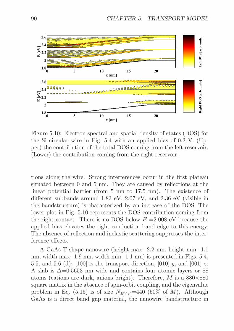
90 CHAPTER 5. TRANSPORT MODEL
0 5 10 15 201.8
2
2.2
2.4
2.6
x [nm]
E [
eV]
0 5 10 15 201.8
2
2.2
2.4
2.6
x [nm]
E [
eV]
Lef
t D
OS
[arb
. uni
ts]
Rig
ht D
OS
[arb
. uni
ts]
Figure 5.10: Electron spectral and spatial density of states (DOS) forthe Si circular wire in Fig. 5.4 with an applied bias of 0.2 V. (Up-per) the contribution of the total DOS coming from the left reservoir.(Lower) the contribution coming from the right reservoir.
tions along the wire. Strong interferences occur in the first plateausituated between 0 and 5 nm. They are caused by reflections at thelinear potential barrier (from 5 nm to 17.5 nm). The existence ofdifferent subbands around 1.83 eV, 2.07 eV, and 2.36 eV (visible inthe bandstructure) is characterized by an increase of the DOS. Thelower plot in Fig. 5.10 represents the DOS contribution coming fromthe right contact. There is no DOS below E =2.008 eV because theapplied bias elevates the right conduction band edge to this energy.The absence of reflection and inelastic scattering suppresses the inter-ference effects.
A GaAs T-shape nanowire (height max: 2.2 nm, height min: 1.1nm, width max: 1.9 nm, width min: 1.1 nm) is presented in Figs. 5.4,5.5, and 5.6 (d): [100] is the transport direction, [010] y, and [001] z.A slab is ∆=0.5653 nm wide and contains four atomic layers or 88atoms (cations are dark, anions bright). Therefore, M is a 880×880square matrix in the absence of spin-orbit coupling, and the eigenvalueproblem in Eq. (5.15) is of size NEV P=440 (50% of M). AlthoughGaAs is a direct band gap material, the nanowire bandstructure in

5.3. RESULTS 91
Fig. 5.5 (d) has strong resemblance to the bulk branches situatedaround the X-point in the three-dimensional Brillouin zone. Manysubbands have a local minimum at k � kmax, where E(k) is close tothe value at k=0. Thus they play an important role in the calculationof the transmission T (E). For example, the minima of the first bandare situated at E(k = 0)=2.236 eV (global, corresponding to the firstturn-on in the electron transmission) and at E(k = 0.92)=2.378 eV(local X-state causing the third, double-degenerate step in T (E)).
Figures 5.4, 5.5, and 5.6 (e) are devoted to a GaAs hexagonalwire (height: 2.4 nm, max width: 2.4 nm, min width: 1 nm) whosetransport direction coincides with [110], y with [110], and z with [001].There are two atomic layers (77 atoms) per slab of width ∆=0.3997nm and 4389 atoms in the nanowire. This is a special case becausethe size of the matrix M involved in the OBCs calculation is thesame as the size of the reduced eigenvalue problem in Eq. (5.15):NM = NEV P=770. This is due to the presence of only two atomiclayers per slab. Both are connected to the neighboring slabs and needto be included in the matrix P defined in Eq. (5.11). All columns of Pwill have at least one element different from zero. The bandstructureand the electron transmission do not exhibit relevant features. Alarger cross section compared to the other nanowires presented inthis work tightens the electron subbands and the transmission growsfaster. With bias, a shift of the curves and a smoothing of the stepsare observed, but no additional effects.
The last GaAs nanowire of Figs. 5.4, 5.5, and 5.6 (f) has a rectan-gular cross section (1.2 nm × 1.2 nm) and a special crystal orientation:x is aligned with [113], y with [110], and z with [332]. Therefore, awire slab (∆=1.8749 nm) contains 22 atomic layers and 140 atoms,3.4 times more than the [100] Si rectangular wire in Fig. 5.4 (a) withthe same dimensions. The matrix M , with size NM=1400, can bereduced according to Eq. (5.15) to NEV P=240, 17.1% of NM . Ournew OBCs method is particularly advantageous when a slab containsmany atomic layers.
The lowest electron subbands in Fig. 5.5 (f) have almost no dis-persion. For example, the first subband starts at E(k = 0)=2.491 eV,goes up to E(k = 0.5)=2.574 eV, and stops at E(k = kmax)=2.512 eV,which represents a bandwidth of 0.083 eV, less than the shift causedby a bias of 0.1 V. This is true for the second subband also. Thus,

92 CHAPTER 5. TRANSPORT MODEL
Figure 5.11: Superposition of an unstrained (black and gray atoms)and of a strained (blue and red atoms) GaAs wire cross section. Theunstrained case corresponds to wire (e) in Fig. 5.4. An homogeneousbiaxial tension is applied in the strain case (εyy = εzz > 0).
when a bias of 0.1 V is applied to the nanowire, the transmission re-mains constant at T (E)=0 instead of turning on at E=2.491+0.1 eV,because the first subband in the left reservoir has already disappearedand the first subband in the right contact does not see any states withthe same symmetry properties. This explains the noisy character ofthe green and red lines in Fig. 5.6 (f).
For nanowires, strain induced by lattice mismatch or growth con-ditions is significant and should not be omitted. Until now, perfectstructures were simulated, but the aim is to show that the approachstill works, if atoms are shifted from their original positions. For thatpurpose, the hexagonal GaAs nanowire introduced in Fig. 5.4 (d) isdeformed. In Fig. 5.11, the original unstrained cross section (blackand gray atoms) is compared to its biaxially deformed counterpart(blue and red atoms). The applied tension increases the cross sectionwhile the width of a wire slab decreases proportionally to the resulting

5.3. RESULTS 93
1.9 2 2.1 2.2 2.3 2.4 2.50
5
10
15
20
E [eV]
Tra
nsm
issi
onno straintensioncompression
1.9 2 2.1 2.2 2.3 2.4 2.50
5
10
15
E [eV]
Tra
nsm
issi
on
no straintensioncompression
Figure 5.12: Electron transmission for the GaAs hexagonal wire inFig. 5.4 without strain (blue lines), with a biaxial tension εyy = εzz =0.015, εxx = −0.0087 (red lines), and for a biaxial compression εyy =εzz = −0.015, εxx = 0.0087 (green lines). (Upper) no bias. (Lower)bias of 0.1 V.
compressive uniaxial strain in the transport direction[54].The strain parameters used in the simulation are found in the
literature[52]. Si examples would be more meaningful, but accordingto our knowledge, there are no published strain tight-binding param-eters for this material that take both Harrison’s scaling rule and theorthogonal character of the Lowdin’s orbitals into account[52]. Thecalculated transmissions are shown in Fig. 5.12. The unstrained (bluelines), tension (red lines), and compression (green lines) cases are com-pared for a flat potential (upper plot) and for a bias of 0.1 V (lowerplot). The biaxial strain amounts to εyy = εzz = ±0.015, the uniaxial,calculated using Van de Walle’s[54] value for D110, to εxx = ∓0.0087.A compressive strain pushes the conduction band edge up, leading toa turn-on of the first channel at a higher energy (E=2.0186 eV) thanwithout strain (E=1.989 eV). In the same way, a tensile strain pushesthe conduction band edge down, leading to a first channel turn-on atE=1.9475 eV. Beginning with the turn-on of the second channel, the

94 CHAPTER 5. TRANSPORT MODEL
2.2 2.3 2.4 2.5 2.6 2.7 2.8 2.9 30
2
4
6
8
10
12
E [eV]
Tra
nsm
issi
onno spinspin
Figure 5.13: Electron transmission through the GaAs T-shape wirein Fig. 5.4 for an applied bias of 0.2 V, calculated with (red dashedline) and without (blue line) spin orbit coupling.
change of the effective mass due to strain compensates the lowering(tension) or increase (compression) of the conduction band edge.
For all the transmission curves in Fig. 5.6, spin-orbit coupling hasbeen neglected, requiring ten atomic orbitals, one s, three p, five d,and one excited s∗. Spin degeneracy could be added by multiplyingeach curve by two for the spin up and the spin down contributions.However, it is legitimate to wonder, if this simplification is justified ornot. First, spin-orbit coupling is more important for GaAs (∆SO=0.34eV) than for Si (∆SO=0.044 eV). Also, its influence is stronger if anon-uniform potential is applied to the nanowire. One compares inFig. 5.13 the electron transmission of the GaAs T-shape wire fromFig. 5.4 (d) in the case of a 0.2 V bias with (red dashed line) andwithout (blue line) spin-orbit coupling. The results match at low en-ergies and slightly differ at higher energies indicating that the neglectof spin-orbit coupling in Figs. 5.5, 5.6, 5.8, 5.9, and 5.12 is a goodapproximation.

5.3. RESULTS 95
Cro
ssse
ctio
n(a
)Sq
uare
(b)
Tri
angl
e(c
)C
ircl
e(d
)T
(e)
Hex
agon
(f)
Squa
reM
ater
ial
SiSi
SiG
aAs
GaA
sG
aAs
xax
is[1
00]
[111
][1
00]
[100
][1
10]
[113
]y
axis
[010
][1
10]
[011
][0
10]
[110
][1
10]
zax
is[0
01]
[112
][0
11]
[001
][0
01]
[332
]W
ire
leng
th[n
m]
22.7
422
.53
22.7
422
.53
22.3
022
.47
Num
ber
ofat
oms
1722
1440
2562
3520
4389
1680
Num
ber
ofsl
abs
4224
4240
5712
Num
ber
ofla
yers
168
144
168
160
114
264
Cel
lw
idth
[nm
]0.
543
0.94
050.
543
0.56
530.
3997
1.87
49Lay
ers
per
slab
46
44
222
Ato
ms
per
slab
4160
6188
7714
0E
Vpr
oble
msi
ze21
016
029
044
077
024
0%
ofno
rmal
size
51.2
26.7
47.5
5010
017
.1ne
wm
etho
d[s
]0.
210.
240.
611.
715.
611.
16Sa
ncho
-Rub
io[4
4][s
]12
.28/
61×
26.5
7/11
0×43
/70×
125/
73×
260/
45×
126.
61/1
09×
GE
VP
[64,
65][s
]6.
39/3
2×17
.05/
70×
24/3
9×74
.28/
43×
67.6
2/12×
212.
09/1
82×
Tab
le5.
2:Tab
lesu
mm
ariz
ing
the
mat
eria
lco
mpo
siti
on,
crys
talor
ient
atio
n,si
ze,an
dat
omic
fitti
ngof
the
nano
wir
espr
esen
ted
inFig
.5.
4.T
heth
ree
last
hori
zont
alen
trie
sco
mpa
reth
eO
BC
sco
mpu
tati
onal
effor
tfo
rth
ene
wca
lcul
atio
nm
etho
dpr
esen
ted
inth
isar
ticl
e,fo
ran
iter
ativ
eal
gori
thm
[44]
labe
led
“San
cho-
Rub
io”
,an
dfo
ra
gene
raliz
edei
genv
alue
prob
lem
(GE
VP
)ap
proa
ch[6
4,65
].In
the
last
two
row
s,th
ese
cond
set
ofnu
mbe
rsgi
ven
besi
deth
eC
PU
tim
esre
fers
toth
esp
eed
degr
adat
ion
ofG
EV
Pan
dSa
ncho
-Rub
iom
etho
dsco
mpa
red
toou
rap
proa
ch.

96 CHAPTER 5. TRANSPORT MODEL
5.3.2 Quantum Well and Mixed Contacts
The transmission coefficient T (E) as well as the density-of-states (DOS)of an unbiased [100] 1.6×1.6×22.5 nm3 Si nanowire are shown in Fig.5.14. Three different cases are presented: (a) the nanowire is coupledto two ideal contacts. The DOS is constant all along the wire, T (E)is a step-like function, each step corresponding exactly to an increaseof the DOS. (b) the Si nanowire is connected to two quantum wellreservoirs. The transmission coefficient exhibits strong interferenceeffects caused by the 2DEG-1DEG transitions. The ideal case (a)forms a kind of upper limit that cannot be exceeded. The nanowire(b) behaves like a resonant cavity delimited by two large areas, thesource and the drain. For example, the cavity eigenmode (obtainedfrom the DOS plot) at E=1.76 eV is symmetric, has two maxima,one around x=5 nm and one around x=17 nm. At E=1.98 eV, amode with five maxima is observed, the three in the middle of thewire being more important than the others. To confirm the resonantcavity hypothesis, in (c), a nanowire with an ideal contact on the left(x=0 nm) and a quantum well contact on the right (x=22.5 nm) isconstructed. The interference effects in the density-of-states and inthe transmission coefficient disappear, proving that they are due toreflections at both ends of the nanowire.
5.3.3 Alloy Disorder
Alloy nanostructures such as AlGaAs nanowires represent a specialchallenge. In effect, the details of disorder are known to be importantat the nanometer scale[53]. In this Section, this issue is addressedby performing atomistic random-alloy calculations of the transportcharacteristics of Al0.15Ga0.85As nanowires with different cross sec-tion sizes. The sp3d5s∗ tight-binding parameters for GaAs and AlAsare taken from Ref. [72]. The wire cross section is a square and itstransport direction x is aligned with [100]. The surface atoms in thex− y and x− z planes are passivated[48] by increasing the dangling-bond energy by 30 eV. The wires are specified in terms of zincblendeconventional unit cubes (side a0=0.56532 nm) as nx×ny ×nz, wherenα is the number of cubes in the α-direction. The wire unit cell corre-sponding to a [100] square cross section is therefore a 1×ny ×nz slab

5.3. RESULTS 97
0 5 10 15 201.7
1.8
1.9
2
2.1
2.2
x [nm]
E [
eV]
0 2 4 6 81.7
1.8
1.9
2
2.1
2.2
TE
E [
eV]
0 5 10 15 201.7
1.8
1.9
2
2.1
2.2
x [nm]
E [
eV]
0 2 4 6 81.7
1.8
1.9
2
2.1
2.2
TE
E [
eV]
0 5 10 15 201.7
1.8
1.9
2
2.1
2.2
x [nm]
E [
eV]
0 2 4 6 81.7
1.8
1.9
2
2.1
2.2
TE
E [
eV]
(a)
(b)
(c)
Figure 5.14: Spatial-spectral density of states (left) and transmissioncoefficient (right) of unbiased [100] 1.6×1.6×22.5 nm3 Si nanowires.(a) with two ideal reservoirs, (b) with two quantum well reservoirs,(c) with an ideal reservoir on the left (x=0 nm) and a quantum wellreservoir on the right (x=22.5 nm).

98 CHAPTER 5. TRANSPORT MODEL
Figure 5.15: Projection onto one atomic plane of a 3.4×3.4 nm2 [100]Al0.15Ga0.85As nanowire slab (blue: Ga atoms, red: As atoms). TheAl atoms (green) are randomly distributed within the slab.
consisting of two pairs of anion-cation planes (four atomic planes).The wires considered here have the dimension 40 × ny × nz.
To construct the Al0.15Ga0.85As nanowires, GaAs structures aregenerated, for which 15% of the Ga atoms are replaced by Al atoms.The position of the Al atoms within a slab is randomly chosen andeach slab is different. This means that both the local arrangement ofatom types and the exact mole fraction (15% Al overall) vary alongthe wire. A 1× 6× 6 slab example is given in Fig. 5.15. 16 Ga atoms(blue) are replaced by Al atoms (green). In this specific slab, thereare only 11.1% of Al atoms so that other slabs will have more than15% of Al atoms.
In the transport calculation, the semi-infinite emitter (collector)region is identical to the first (last) slab of the nanowire. Open bound-ary conditions are obtained as described in Section 5.2. The ran-dom alloy calculations are presented in Fig. 5.16 for a 40 × 6 × 6(22.5×3.4×3.4 nm3, 11520 atoms), a 40 × 8 × 8 (22.5×4.5×4.5 nm3,20480 atoms), a 40×10×10 (22.5×5.7×5.7 nm3, 32000 atoms), and a40×12×12 (22.5×6.8×6.8 nm3, 46080 atoms) Al0.15Ga0.85As nanowire(blue lines). The randomness in the Al atom distribution implies thatpropagating modes in the nanowire differ from slab to slab and that a

5.3. RESULTS 99
1.9 2 2.1 2.20
2
4
6
8
10
12
(a)
E [eV]
TE
random disorderregular disorderVCA
1.8 1.85 1.9 1.95 20
2
4
6
8
10
12
14(b)
E [eV]
TE
random disorderregular disorder
1.7 1.75 1.8 1.85 1.9 1.950
2
4
6
8
10
12(c)
E [eV]
TE
random disorderregular disorder
1.7 1.75 1.8 1.85 1.90
5
10
15
20(d)
E [eV]
TE
random disorderregular disorder
Figure 5.16: Transmission through 22.5 nm long Al0.15Ga0.85Asnanowires (40 slabs in the transport direction). Blue lines stand forrandom disorder of Al atoms, green lines for nanowires made out of 40identically disordered slabs, and the red line corresponds to the virtualcrystal approximation. (a) 3.4×3.4 nm2 cross section (11520 atoms),(b) 4.5×4.5 nm2 (20480 atoms), (c) 5.7×5.7 nm2 (32000 atoms), and(d) 6.8×6.8 nm2 (46080 atoms).
step-like function of energy cannot be expected for the transmission.To demonstrate further that the randomness along the device is
responsible for the noisy transmission behavior described above, thetransmission coefficients of ordered Al0.15Ga0.85As with 40 identicalslabs are also calculated (green lines in Fig. 5.16). In the absenceof slab variations the transmission behavior is characterized by thesmooth plateaus found in pure and unbiased GaAs or Si nanowires inFig. 5.6.
A simplified approach to treat alloy nanostructures is the so-calledvirtual crystal approximation (VCA). In the VCA calculation, the

100 CHAPTER 5. TRANSPORT MODEL
cations are all fictitious Al0.15Ga0.85 pseudo-atoms and all on-siteand nearest-neighbor parameters are weighted averages of those forAlAs and GaAs. An example is given in Fig. 5.16 (red line). TheVCA transmission shows noiseless, step-like turn-ons of channels andit overestimates the random alloy band gap[73]. This is a severe short-coming because the transmission at the lowest energies profoundly af-fects the transport properties of nanowires. Further details about theelectronic structure and the transmission characteristics of disorderedAlGaAs nanowires can be found in Refs. [74, 75].
5.4 Discussion
In Section 5.2 it was stated that the new approach to calculate openboundary conditions (OBCs) is more efficient than other methodsfound in the literature[44, 64, 65, 68, 70, 76, 77]. To support this claim,other available methods are classified into three categories: first, thereare the solutions that do not work for nanowires because they re-quire the inversion of singular matrices to generate a generalized[76]or a normal[70] eigenvalue problem whose size is in any case largerthan Eq. (5.15). Secondly, the transformation of Eq. (5.6) to a com-plex non-hermitian (if spin-obit coupling is included) or real non-symmetric (without spin-orbit coupling) generalized eigenvalue prob-lem (GEVP) as in Eq. (5.7) is very popular[64, 65, 68, 77], since itcan be coupled to Wave Function[64] or to Non-equilibrium Green’sFunction (NEGF)[65] transport solvers. Nevertheless, if a nanowireslab contains N atoms and tb is the tight-binding order, the size ofthe GEVP amounts to NGEV P = 2tbN , a considerable number inthe case of large cross sections and transport directions different from[100]. LAPACK[78] functions can be used to solve Eq. (5.7). Finally,the third category includes the OBCs calculation with an iterativealgorithm[44]. In this case, very dense or even full matrices of sizeNM = tbN must be inverted 20 to 40 times to reach convergence.This approach works only to obtain the boundary self-energies in theNEGF formalism.
In Table 5.2, the computational time for the generalized eigen-value problem, the iterative scheme (labeled “Sancho-Rubio”), andthe new method are reported, as well as the speed-up factor achieved.

5.4. DISCUSSION 101
All methods have been implemented in MATLAB[79] because it au-tomatically calls LAPACK routines to solve the eigenvalue problemsand to invert matrices. Although the CPU times would be faster ifthe codes were written in C++, a relative comparison of the differentmethods makes sense in MATLAB, too. The benchmark examplesare run on the same hardware platform. The CPU times in Table 5.2(three last lines) refer to the OBCs calculation of one single contactat one given injection energy, without spin-orbit coupling (real EVP),and where the simplification depicted in Fig. 5.2 is not applied. Notethat the computational burden in the iterative algorithm case dependson the injection energy and could be, therefore, more important thanwhat is given in Table 5.2. The methods based on eigenvalue prob-lems require the same effort for all the energies and among them ourapproach is always the most efficient with a OBCs computational timeat least one order of magnitude below the others.
For transport directions such as [111] or [113], the improvement islarger because a wire slab contains many atomic layers that can bedisregarded in the OBCs calculation (see the line labeled “% of normalsize” that indicates what part of matrix M is effectively consideredin the reduced EVP). Even for the less advantageous case where x isaligned with [110] (only two atomic layers per slab), Eq. (5.15) is themost appropriate solution. Rivas et al. mentioned[65] that the GEVPapproach is more efficient than iterative methods[44] since it doesnot involve repetitive calculations. This is confirmed by the results(a factor 1.5-4), except when x coincides with [113] where GEVP isslower.
After the OBCs are calculated with Eq. (5.15), it is possible tocouple them either to the linear system of equations (5.17) or totransform them to self-energies with Eq. (5.25) in order to simulatetransport. In the Wave Function approach, one proceeds to a LUfactorization of Eq. (5.17), because it can be done in parallel[80] onseveral CPUs. More sophisticated linear solvers such as SPIKE[81]could be used for that purpose. In the NEGF formalism one utilizes arecursive algorithm[14, 23] that is slower than the LU factorization ofEq. (5.17), even on one single CPU, since it requires the inversion ofNS (number of wire slabs) matrices of size NM = tbN . However, theGreen’s function method facilitates the inclusion of inelastic scatter-ing. To improve both the Wave Function and NEGF approaches one
102 CHAPTER 5. TRANSPORT MODEL
can reduce the bandwidth of the tight-binding Hamiltonian matrix.All the elements Dii, Tii+1, and Tii−1 are expressed in a slab basis,but there is no restriction to change it and to use an atomic layerbasis, as for the boundary conditions. The block matrices that mustbe inverted in the NEGF recursive algorithms become smaller and theLU factorization works better.
5.5 Summary
This Chapter presented simulation approaches for nanowires with two-dimensional confinement. At the atomic scale, bandstructure effectsplay an important role and must be treated carefully. One has de-veloped a quantum transport simulator based on the sp3d5s∗ semi-empirical tight-binding method in order to improve the understandingof the electrical behavior of such structures. Since the calculation ofthe open boundary conditions causes a significant part of the compu-tational burden, a new method involving the solution of a complexnon-hermitian or real non-symmetric eigenvalue problem is proposed.It works for Si, GaAs, or for any other material, for different crosssections and crystal orientations, for disordered nanowires, when abias is applied or not, when the structure is deformed by strain, andwhen non-ideal contacts are used. A factor 10 to 100 compared tothe other available methods could be gained in the evaluation of theOBCs, enabling the treatment of larger and more complicated struc-tures. The coupling of the new approach to a Wave Function and toa NEGF quantum transport solver has also been presented.

Chapter 6
Self-ConsistentSimulations
6.1 Introduction
In this Chapter the room temperature IV-characteristics of Si triple-gate nanowire field-effect transistors (FET) are simulated for differ-ent channel orientations such as [100], [110], [111], and [112]. Thefull-band (FB) properties of Si are taken into account via the semi-empirical nearest-neighbor sp3d5s∗ tight-binding method. The three-dimensional (3D) electrostatic potential (Poisson’s equation) is solvedself-consistently with the device charge density. Previous ’top-of-the-barrier’ approaches[82] considered a one-dimensional electrostatic po-tential only and semi-classical transport, but they gave a good insightinto the device IV-characteristics. However, their application is re-stricted to the ballistic transport of perfect atomic structures (no spa-tial variation of the nanowire cross section), whose energy dispersionrelation (E−k) can be calculated. Our simulator furthermore includesshort channel effects such as drain induced barrier lowering, tunnelingthrough the barrier, lateral potential variation, and allows to treat Si-SiO2 interface roughness at the nanowire surface. Energy relaxationof the atom positions is out of the scope of this work. To emphasizethe importance of full-band simulations, the IV-characteristics of a
103

104 CHAPTER 6. SELF-CONSISTENT SIMULATIONS
[100] channel-oriented wire are compared to effective mass (EM) cal-culations obtained by the three-dimensional coupled mode-space Non-Equilibrium Green’s Function (NEGF) solver presented in Chapter 3.
6.2 Theory
The multi-band quantum transport simulator presented in Chapter5 is coupled to a three-dimensional Poisson solver using an iterativeNewton scheme. To describe the nanowire structures, the same con-ventions as in Fig. 5.1 are used. The transport direction x determinesthe channel orientation, y and z are directions of confinement. Eachnanowire can be divided into slabs (wire unit cell) of width ∆. Theslabs are made out of atomic layers (all the atoms with the same xcoordinate), whose number is related to the transport direction (4 for[100], 2 for [110], 6 for [111], and 6 for [112]). In the ’top-of-the-barrier’approach all the slabs are identical, but computing a 3D electrostaticpotential allows for the number of atoms per slab and the shape of aslab to vary along the nanowire channel.
Due to the very localized character of the Lowdin orbital functionsφσ(r− ri) used in the tight-binding method, the electron charge n(r)(holes are not considered in the simulations) and the current J(r)densities are represented by δ-functions centered around the atompositions ri (see the justification in Section 5.2.1)
n(r, t) =∑i
niδ(r− ri), (6.1)
J(r, t) =∑i,j
Iij(rj − ri)δ(r− ri). (6.2)
Bold letters denote vectors, ni is the number of electrons at ri, Iij isthe current flowing from one atom situated at ri to its nearest neighborat rj (in principle four different j per i) along the bond connectingthem.
To prove the ansatz (6.1) and (6.2), the definitions of n(r, t) andJ(r, t) in Eqs. (2.60) and (2.65), as well as the 3D tight-bindingexpression of the Green’s function in Eq. (2.35) are recalled. Forsimplicity, the orbital type index σ and the position indices xi, yj ,
6.2. THEORY 105
and zk are put into a single index i. This gives
n(r) = −i�∑i1,i2
G<i1i2φi1(r− ri1)φ∗i2(r− ri2)
≈ −i�∑i1
G<i1i1
|φi1(r− ri1)|2
≈ −i�∑i1
G<i1i1δ(r− ri1) (6.3)
for the carrier density. Eq. (6.3) corresponds to Eq. (5.19) rewrittenin the NEGF formalism. For the current density one obtains
J(r) = e�2
2m0
∑i1i2
G<i1i2
limr′→r
(∇r′ −∇r)φi1(r− ri1)φ∗i2(r′ − ri2)
= ie�
2m0
∑i1i2
G<i1i2
limr′→r
(p′ − p)φi1(r− ri1)φ∗i2(r′ − ri2)
= e2
∑i1i2
G<i1i2
limr′→r
([H0, r] − [H0, r′])φi1(r− ri1)φ∗i2(r′ − ri2)
≈ e2
∑i1i2
(ri2 − ri1)(Hi1i2G
<i2i1
−G<i1i2Hi2i1
) |φi1(r− ri1)|2≈∑
i1
∑i2
e
2(Hi1i2G
<i2i1
−G<i1i2Hi2i1
)︸ ︷︷ ︸
Ii1i2
(ri2 − ri1)δ(r− ri1).
(6.4)The time-dependence of the different variables is omitted for brevity.The transition from the third to the fourth step in Eq. (6.4) is accom-plished by multiplying the equality with the following unity operators∫
dr1 δ(r− r1) =∫
dr1∑n
φn(r− rn)φ∗n(r1 − rn)
∫dr2 δ(r′ − r2) =
∫dr2∑n
φn(r2 − rn)φ∗n(r′ − rn) (6.5)
resulting from the orthogonality and the completeness of the tight-binding basis. The matrix elements Hi1i2 , defined as in the Slater-Koster table[32], represent the coupling between an orbital of type σ1
106 CHAPTER 6. SELF-CONSISTENT SIMULATIONS
situated on an atom at {xi1yj1zk1} and an orbital of type σ2 on anatom at {xi2yj2zk2}. In the nearest-neighbor approximation one atomis connected to the maximum of four other atoms. Thus (ri2 − ri1)in Eq. (6.4) is nothing else than the bond vectors bαi introduced inChapter 4.
In the ballistic regime or in the absence of inelastic scattering thesteady-state current density is often calculated with the Landauer-Buttiker formalism[69] which does not allow to check current conti-nuity, as mentioned in Chapter 3. In Eq. (6.4) it is also very diffi-cult to see, if the current is correctly evaluated or not, because onlyatomic contributions are present. However, the slab structure of thenanowires and the assumption that the current flows between two con-tacts only, the source and the drain, enable another approach. Thesteady-state current Id(xn) flowing through the slab n can be com-puted by integrating the x-component of the current density J(r) overthe cross section of the slab n. This is equivalent to integrate Jx(r)over the volume V of the slab n and to divide the result by the slabwidth ∆
Id(xn) =1∆
∫Slab n
dV Jx(r). (6.6)
If Eq. (6.4) is inserted into Eq. (6.6) and if the steady-state, energy-dependent form of the Green’s functions is used, the following expres-sion is found for Id(xn)
Id(xn) =e
�
∫dE2π
tr(Hnn+1G<
n+1n(E) −G<nn+1(E)Hn+1n
). (6.7)
The matrix Hnn+1 (Hn+1n) couples the slab n (n + 1) to the slabn+ 1 (n). If there are Nn atoms in the slab n and Nn+1 atoms in theslab n+1, the size of Hnn+1 and of G<
nn+1 is (Nntb)× (Nn+1tb). Theparameter tb, as usual, is the tight-binding order. In Appendix C atransformation is proposed to express the Green’s function G<
nn+1(E)in the Wave Function formalism.
With Eq. (6.7) it can be verified whether the current Id(xn) inthe slab n and the current Id(xn+1) in the slab n + 1 are equal forall the n’s. If this condition is not satisfied, the calculations are not

6.2. THEORY 107
correct and the presence of a mistake in the simulator implementationis clearly indicated.
To solve the three-dimensional Poisson equation in the nanowireFETs without loosing the δ-character of the carrier density, the finiteelement method (FEM) is chosen[83, 84]. A Delaunay grid is con-structed with the property that no atom is contained in the volume ofany tetrahedron mesh element. The atom positions are given as inputparameter to the Qhull mesh generator[85], which use them as fixednodes. The δ-functions thus disappear when the electron density n(r)is integrated with the FEM test functions.
The SiO2 oxide layers do not participate to the transport calcula-tion (only poor tight-binding representation available), but they areincluded in the 3D electrostatic potential solved in the Poisson equa-tion. Consequently, the oxide grid points carry no charge and hardwall boundary conditions are applied to the Si surface atoms. Thismeans that the Si dangling bonds are passivated by increasing theon-site energies of the s- and p-orbitals[48].
The nanowire roughness effects are generated by randomly dis-tributing the atoms at the Si-SiO2 interface according to an exponen-tial autocovariance function Γs(x)[86]
Γs(x) = ∆2m · e−|x|/Lm (6.8)
where ∆m is the root mean square of the Si rough surface s(r), x isthe distance between two Si atoms at the Si-SiO2 interface, and Lm
is the correlation length of the roughness. Note that the√
2 factorpresent in Ref. [86] is absent in Eq. (6.8).
To construct s(r), the positions ri of the Si atoms at the nanowiresurface are selected. Each nanowire face is treated independently.It is assumed that s(r) is a stationary Gaussian process so that thespecification of its autocorrelation function in Eq. (6.8) completelydefines its probability density function (p. d. f.)[87]. If a nanowireface has N atoms, the p. d. f. of its variations is given by
p(s(r1), · · · , s(rN)) =1
(2π)N/2|C|1/2 exp[−12STC−1S]. (6.9)
The N×1 vector S = (s(r1), · · · , s(rN))T contains the variation of thesurface at each atom position ri. The elements Cij of the symmetric

108 CHAPTER 6. SELF-CONSISTENT SIMULATIONS
matrix C represent the correlation between s(ri) and s(rj)
Cij = 〈s(ri)(s(rj)〉 = ∆2m · e−|ri−rj|/Lm . (6.10)
Since all the variables in Eq. (6.9) are coupled, it is not obvious tofind a realization of S without a basis change. For that purpose theeigenvalues (diagonal ofD) and the eigenvectors (V) of the correlationmatrix C = V ·D·VT are calculated, the vector S = V ·S is expressedin a new basis, and a simplified p. d. f. is obtained
p(s(r1), · · · , s(rN)) =1
(2π)N/2|D|1/2 exp[−12STD−1S]
=N∏i=1
1√2πσi
exp[− s2(ri)2σ2
i
], (6.11)
where the elements Dii = σ2i of the diagonal matrix D correspond
to the variance of each variable s(ri). S is realized with a randomnumber generator and it is transformed back to the original basisS. Finally, for a given nanowire face, the variation of the surface isstudied at each Si atom position ri. If s(ri) is positive and largerthan the distance between two atoms, new atoms are added to thestructure. In the case of a negative s(ri), but with an absolute valuelarger than the distance between two atoms, atoms are removed fromthe structure.
6.3 Results
The upper part of Fig. 6.1 shows the schematic view of a triple-gatenanowire transistor of length Ls + Lg + Ld ≈ 32 nm, composed ofn-doped source and drain contacts (ND=1020 cm−3, stoichiometricratio f=2×10⁻³ of fully ionized donors) and a three-part gate (top,left, and right). The transistor is deposed on a buried oxide and issurrounded by three oxide layers of thickness tox=1 nm. The source,the drain, and the gate measure Ls=10 nm, Ld=10nm, and Lg=12nm, respectively. x is the transport direction, y and z are directionsof confinement. The cross section of the nanotransistor (neglectingthe buried oxide) has a size Ly=4.1 nm times Lz=3.1 nm. Two cross

6.3. RESULTS 109
Lz
Vs
Si
SiO
2
Sou
rce
Vg G
ate
Dra
inV
d
Bu
ried
Oxid
e
Ls
Lg
Ld
x y
z
Lz
Ly
Ly t o
x
t ox
t ox
t ox
t ox
t ox
Lz
Ly
Fig
ure
6.1:
Sche
mat
icvi
ewof
atr
iple
-gat
eSi
nano
wir
etr
ansi
stor
110 CHAPTER 6. SELF-CONSISTENT SIMULATIONS
sections corresponding to different channel orientations are given inthe lower part of the figure. In the left subplot, x is aligned with [100]and in the right subplot with [110]. Points represent Si atoms whilelines model atomic bonds. The SiO2 layers are not described in thetight-binding formalism. The nanowire channel (only Si atoms) is a2.1 nm x 2.1 nm square. A potential Vg is applied to the gate (workfunction φm=4.25 eV), Vs=0 V to the source and Vd to the drain.
Channel orientations along [100], [110], [111], and [112] are consid-ered. The resulting nanowires contain about 7300 atoms. The [100]channel is composed of 60 slabs of width ∆=0.543 nm (transistorlength=60×∆=32.6 nm), each slab has 4 atomic layers and is madeout of 128 atoms. For the [110] channel, 84 slabs of width ∆=0.384nm are counted, each of them with 2 atomic layers and 88 atoms. The[111] channel contains 34 slabs (∆=0.941 nm) with 6 atomic layers(210 atoms) per slab. Finally 49 slabs (∆= 0.665 nm) are present inthe [112] wire, each of them has 6 atomic layers and 154 atoms.
On the left side of Fig. 6.2, the FB (solid lines) and the EM (dashedlines) Id−Vds current characteristics at three different Vgs (0.5 V, 0.55V, and 0.6 V) are compared for a wire with a [100]-oriented channel.Due to the absence of non-parabolicity effects in the EM case, currentchannels turn on more slowly than in the FB case. This can be seenin Fig. 6.3, where the total transmission coefficient T (E) from sourceto drain is plotted for Vgs=Vds=0.4 V. The first four channels of theFB transmission (blue line) appear earlier and increase faster thanin EM calculation (green line). Consequently, the drain current Id isunderestimated by about 15% in the EM case.
On the right-hand side of Fig. 6.2, one simulates the 3D full-bandId − Vgs (Vds=0.4 V) transfer characteristics of the nanodevices with[100] (blue line), [110] (red line), [111] (green line), and [112] (orangeline) channel orientations. The comparison is done for the same gatemetal work function φm=4.25 eV. This means that φm is not adjustedto obtain the same OFF-current (IOFF = Id at Vgs=0 V and Vds=0.4V) as done in Ref. [82].
The transistor ON-current ION is reached when the gate-controlledpotential barrier that blocks the source to drain channel disappears.This is the case, for example, at Vgs=0.7 V in the right subplot ofFig. 6.2. It is normally expected that at Vgs=Vds, the drain current Idis already above threshold. Obviously, Id at Vgs=0.4 V lies in the sub-

6.3. RESULTS 111
0 0.1 0.2 0.3 0.4 0.50
0.5
1
1.5
Vds
[A]
I d [
µA]
0 0.1 0.2 0.3 0.4 0.5 0.6 0.710
−10
10−8
10−6
10−4
10−2
100
102
Vgs
[V]I d
[µA
]
FB [110] Vds
=0.4 VFB [100] V
ds=0.4 V
FB [111] Vds
=0.4 VFB [112] V
ds=0.4 V
Vg=0.5 V
Vg=0.55 V
Vg=0.6 V
Figure 6.2: Output and transfer characteristics of triple-gate nanowiretransistors. The left subplot compares the Id − Vds of a [100] channelat three different Vgs , obtained with full band (FB, solid lines) andwith the effective mass approximation (EM, dashed lines). The rightsubplot shows the Id−Vgs results at Vds=0.4 V for transport directionsalong x=[100] (FB: blue line), x=[110] (FB: red line), x=[111] (FB:green line), and x=[112] (FB: orange line).
1.5 1.6 1.7 1.8 1.9 2 2.10
1
2
3
4
5
6
7
8
9
10
E [eV]
T(E
)
FB T(E) Vds
=Vgs
=0.4 VEM T(E) V
ds=V
gs=0.4 V
FB+EM Source Fermi Energy
Figure 6.3: Transmission coefficient T(E) through the [100] nanowireat Vgs=Vds=0.4 V calculated with full band (FB: blue line) and withthe effective mass approximation (EM: green line) when both FB andEM source Fermi levels (vertical red line) are aligned.

112 CHAPTER 6. SELF-CONSISTENT SIMULATIONS
Channel [110] [100] [112] [111]ION [µA] 7.7 4.3 2.9 1.2
Table 6.1: ON-Current ION=Id at Vgs=0.7 V and Vds=0.4 V for theSi nanowire transistors described above.
threshold region since the threshold voltage Vth is situated betweenVgs =0.45 V and Vgs =0.5 V, depending on the channel orientation.However, the choice of another gate material with a lower work func-tion (n-doped poly-silicon gates have a work function φm=4.05 eV)will decrease Vth.
As predicted by the ’top-of-the-barrier’ approach[82], the channelorientation [110] (red line) offers the highest ON-current ION taken atVgs=0.7 V and Vds=0.4 V, 1.8 times higher than [100] (blue line), 2.6times higher than [112] (orange line) and 6.5 times higher than [111](green line). The values are summarized in Table 6.1. The prominenceof the [110] channel is a consequence of the compromise between theelectron velocity (proportional to the inverse of the effective mass)and the number of available states (proportional to the effective mass)that is reached by the lowest conduction subbands of the [110] wire.The lowest [111] conduction subbands, for example, have too heavyelectrons that cannot flow efficiently from source to drain. The sub-threshold swing S of the four nanowires is very close to its ideal valueof S=60 mV/decade (less than 1% difference).
Nanowires with a perfect crystal structure and a well-defined Si-SiO2 interface will probably never be grown. The inclusion of the 3Delectrostatic potential makes it possible to simulate wires with a crosssection (or slab contour) that varies from source to drain[88, 89]. Theexample of a non-ideal wire slab (channel orientation x=[100]), takenunder the gate at the slab position 35 over 60, is given in Fig. 6.4.The atom positions in the middle of the slab are all occupied. Atthe Si-SiO2 boundary some atoms are randomly removed others areadded to form a rough interface. Therefore, slab 35 includes 123 atomsinstead of 128 as in the ideal case in Fig. 6.1. As a first approximationthe root mean square of the Si rough surface ∆m=0.14 nm and thecorrelation length Lm=0.7 nm are the same for all the surface types([100], [110], [111], and [112]).

6.3. RESULTS 113
Since all the nanowire slabs are different, it is not possible to firstconstruct a two-dimensional mesh with triangle elements on each slaband then to interpolate between the slab meshes to obtain tetrahedra.A full 3D FEM mesh, as projected in Fig. 6.4, must be generated tocalculate the electrostatic potential V (r). The mesh elements are fineraround the atoms than in the oxide layers, where V (r) varies linearlydue to the absence of charge (the second derivative of V (r) vanishes).
In Fig. 6.5, the full-band Id − Vgs (Vds=0.4 V) transfer charac-teristics of a [100] (blue lines) and a [110] (red lines) structure withinterface roughness (dashed lines) are compared to the results of idealstructures (solid lines). For the simulated realizations of the randomSi-SiO2 interface, the [100] drain current Id at Vgs=0.4 V is reducedto about 30% of its ideal value, the [110] drain current at Vgs=0.4 to65% of the ideal Id. The drain current in the sub-threshold region isseriously deteriorated by the variation of the nanowire cross section.This is due to a mobility decrease caused by interface roughness scat-tering. At the same time, the oxide thickness tox is modulated, leadingto a shift of the threshold voltage Vth, but the swing S remains closeto S=60 mV/decade (the current is controlled by the barrier height).Such non-ideal effects could not be observed with a ’top-of-the-barrier’approach[82].
However, another random distribution of the interface atoms leadsto a different transfer characteristics Id−Vgs. Since the sub-thresholdswing S is not much affected by the interface roughness, several Idsamples can be calculated at a fixed Vgs and the variations of thethreshold voltage Vth is extrapolated from the results. For each chan-nel orientation, 105 different Si-SiO2 interface realizations are simu-lated, the mean drain current Id is calculated, and the variation ofVth is obtained for each sample Id as
∆Vth = S · log10
(Id/Id
). (6.12)
The histogram distributions of ∆Vth are shown in Fig. 6.6 for the [110](red bars), the [100] (blue bars), the [111] (green bars), and the [112](orange bars) nanowires. The standard deviation σ of ∆Vth is alsogiven for each channel configuration.
To design a circuit, all the involved transistors should have thesame characteristics although they have slightly different structures.

114 CHAPTER 6. SELF-CONSISTENT SIMULATIONS
Figure 6.4: Projection of the slab number 35 of the [100] nanowiretransistor with interface roughness. Bullets are Si atoms, lines repre-sent the projection of the three-dimensional Delaunay finite element(FEM) mesh used to compute the self-consistent electrostatic poten-tial.
0 0.1 0.2 0.3 0.4 0.5 0.610
−10
10−8
10−6
10−4
10−2
100
Vgs
[V]
I d [µA
]
FB [100] Vds
=0.4 V: Si−SiO2 Int. Rough.
FB [100] Vds
=0.4 V: perfectFB [110] V
ds=0.4 V: Si−SiO
2 Int. Rough.
FB [110] Vds
=0.4 V: perfect
Figure 6.5: Full-band transfer characteristics Id − Vgs at Vds=0.4 Vfor perfect [100] and [110] nanowires (solid lines) and for [100] and[110] nanowires with Si-SiO2 interface roughness (dashed lines).

6.3. RESULTS 115
−40 −20 0 20 400
5
10
15
20
25(b)
∆Vth
[mV]
Sam
ples
−30 −20 −10 0 10 20 300
5
10
15
20(a)
∆Vth
[mV]
Sam
ples
−60 −30 0 30 600
5
10
15
20
25(c)
∆Vth
[mV]
Sam
ples
−40 −20 0 20 400
5
10
15
20(d)
∆Vth
[mV]
Sam
ples
σ=9.3 mV σ=13.8 mV
σ=24.8 mV σ=16.8 mV
Figure 6.6: Histogram distribution of 105 samples representing thevariation of the threshold voltage ∆Vth caused by interface roughness.The results for the (a) [110], (b) [100], (c) [111], and (d) [112] Sinanowire transistors are plotted. σ is the standard deviation of ∆Vth.

116 CHAPTER 6. SELF-CONSISTENT SIMULATIONS
Hence the standard deviation of ∆Vth should be as small as possible.The lowest value of σ is obtained for a channel oriented along the [110]crystal axis (σ=9.8 [mV]). [100] follows with σ=13.8 [mV], then [112](σ=16.8 [mV]), and [111] (σ=24.8 [mV]). [110] is definitively the bestchannel orientation because it has the highest ON-current and it isthe least sensitive to structure variations.
All the Id samples calculated to generate the histograms in Fig. 6.6must fulfill current continuity. This very important property in thesimulation of ballistic transistors should not be altered by interfaceroughness. To demonstrate its validity the current Id flowing fromone nanowire slab to the other is reported in Fig. 6.7 for Vds=0.4 Vand for different Vgs. Id(xn) is calculated in a non-ideal [100] nanowirewith Eq. (6.7). Although the nanowire transistor is composed of slabswith different shapes and with a different number of atoms, the currentis conserved in our approach.
Finally, Fig. 6.8 shows how interface roughness affects the elec-tron distribution in the [100] transistor. Because of the δ-character ofthe electron density n(r), only the total number of electrons in eachwire slab can be plotted. The number of electrons per slab with in-terface roughness depends on three different effects: the electrostaticpotential, the confinement of the y and z directions, and the conduc-tion band edge lowering or increase caused by the modifications ofthe slab shapes (red line in Fig. 6.8). For example, in the slab 27,the conduction band edge is lowered by the roughness so that moreelectrons are present in the non-ideal structure (blue line) than in theideal one (dashed green line). In the slab 33, the contrary effect oc-curs. As a consequence of the conduction band increase, a reductionof the electron population is observed.
6.4 Summary
In this Chapter, full-band simulations of ballistic Si nanowire transis-tors with different channel orientations were presented. The electronand the current densities are calculated either with NEGF, introducedin Chapter 2 or with the Wave Function formalism. In both cases thesemi-empirical sp3d5s∗ tight-binding method, summarized in Chapter4, is included in the transport calculation via the approach described

6.4. SUMMARY 117
0 10 20 30 40 50 6010
−10
10−8
10−6
10−4
10−2
100
Slab Position
I d [µA
]
Vgs
=0.0 V, Vds
=0.4 V
Vgs
=0.1 V, Vds
=0.4 V
Vgs
=0.2 V, Vds
=0.4 V
Vgs
=0.3 V, Vds
=0.4 V
Vgs
=0.4 V, Vds
=0.4 V
Vgs
=0.5 V, Vds
=0.4 V
Vgs
=0.6 V, Vds
=0.4 V
Figure 6.7: Full-band transfer characteristics Id − Vgs at Vds=0.4 Vplotted along the [100] nanowire (60 slabs) with Si-SiO2 interfaceroughness.
0 10 20 30 40 50 6010
−4
10−3
10−2
10−1
100
Nu
mb
er o
f E
lect
ron
s p
er S
lab
FB roughness, Vgs
=0.5 V, Vds
=0.4 VFB perfect, V
gs=0.5 V, V
ds=0.4 V
0 10 20 30 40 50 60
−0.05
0.00
0.05
0.10
0.15
Slab Position
Con
du
ctio
n B
an
d E
dge
Vari
ati
on
CB variations
Slab 27
Slab 33
Figure 6.8: Number of electrons per nanowire slab at Vds=0.4 V andat Vgs=0.5 V for the [100] nanowire transistor with perfect Si-SiO2
interface (dashed green line) and with interface roughness (IR, blueline). The red line describes the variation of the confinement potentialdue to IR.

118 CHAPTER 6. SELF-CONSISTENT SIMULATIONS
in Chapter 5. The results are obtained by self-consistently couplingthe calculation of the three-dimensional electrostatic potential in thedevice and of the induced charge density. New effects such as Si-SiO2
interface roughness are then studied on an atomic scale.The full-band current characteristics of a Si nanowire transistor
whose channel is aligned with [100] are first compared to results ob-tained with the effective mass approximation, presented in Chapter3, and then to the characteristics of Si nanowires with other channelorientations ([110], [111], and [112], all with full-band). It is con-cluded that the effective mass current is underestimated due to theabsence of non-parabolicity effects and that [110] is the most favorablechannel orientation in Si nanowire. In effect, it provides the highestON-current and it is less affected by deformations of the atomic struc-ture. This should be confirmed by comparison with measurement.

Chapter 7
Conclusion and Outlook
In this thesis, a full-band formalism was developed to simulate nano-wire transistors at the atomic scale, including a new procedure to cal-culate the open boundary conditions. It was then applied to aggres-sively scaled triple-gate FETs with different channel orientations. De-spite the promising results obtained with the current simulator, somephysical issues should be further investigated for future improvement.
In the nanowire structures described in Chapter 6, the dopingconcentration is equally distributed in the source and drain regions.However it would be more meaningful to treat each doping atom indi-vidually and to carefully describe them in the transport calculation.Accurate tight-binding parameters are required for that purpose. Thisconcerns also the SiO2 oxide layers that appears only in the calcula-tion of the electrostatic potential. In this way, no electron penetrationin the oxide is allowed and the surface Si atoms are artificially passi-vated. Furthermore, gate leakage currents, which are a performancelimiting factor for very thin oxide layers, cannot be taken into account.As a consequence, the OFF-current of the transistors is not correctlymodeled.
When the nanowire cross sections are small, as in our examples,the surface atoms relax from their “equilibrium” position in order tominimize the total energy of the system. This is particularly truewhen single atoms are added or removed at the surface. These effectsare not considered in this work, but they are certainly important,
119

120 CHAPTER 7. CONCLUSION AND OUTLOOK
especially in the case of an atomic description of SiO2.Scattering mechanisms may play a considerable role in nanowires
transistor, but they are not treated in this work, with the exception ofalloy disorder and interface roughness. Both of them can be directlyincluded in the Hamiltonian matrix, which is not the case for inelasticinteractions such as electron-optical phonon scattering. This compli-cated effect must be probably included via self-energies as describedin Chapter 2. The use of confined phonons instead of bulk phononsbecomes necessary at the atomic scale.
The full-band simulator presented in this thesis has also the ca-pability of treating mechanical strain and other materials than Si(GaAs, Ge, InAs, ...). However, it is limited by the dimension ofthe nanowire cross section and its inherent computational burden.Each injection energy requires the solution of two eigenvalue prob-lems for the open boundary conditions and of one linear system forthe transport through the nanowire. These tasks can be distributedon parallel CPUs, each of them working on a different energy point,but for large cross sections, due to memory restriction, a group ofCPUs has to be dedicated to one single energy. If a computer clusterwith several hundreds of CPUs is available, it is possible to simulateany transistor structure. On the other hand, as the cross section ofthe structure grows, the effective mass approximation becomes moreand more accurate and requires much less computational power. Theuser will have to determine which method is the more indicated forhis application.

Appendix A
InteractionRepresentation
The Non-Equilibrium Green’s Functions are defined in the Heisenbergpicture. However, a representation in the interaction picture gives abetter insight into their time evolution. In this Appendix we presentthe different pictures in which operators and wave functions can beexpressed. The system under consideration is governed by a time-independent Hamilton operator H = H0 + V . The eigenvalues andeigenvectors of H0 are known, V is a perturbation .
A.1 Schrodinger Picture
In the Schrodinger picture, the operators OS are time-independent.The time-dependence is contained in the wave functions |ΨS(t)〉, ob-tained in the Schrodinger equation
i�ddt
|ΨS(t)〉 = H|ΨS(t)〉 (A.1)
with the formal solution
|ΨS(t)〉 = e−iH(t−t0)/�|ΨS(t0)〉 = e−iH(t−t0)/�|Ψ0〉, (A.2)
describing the time evolution of the initial state |Ψ0〉 from t0 to t.
121

122 APPENDIX A. INTERACTION REPRESENTATION
A.2 Heisenberg Picture
In the Heisenberg representation, the operators are time-dependent,but not the wave functions, given by
|ΨH(t)〉 = eiH(t−t0)/�|ΨS(t)〉 (A.3)= |ΨH(t0)〉 = |Ψ0〉
because
ddt
|ΨH(t)〉 =i
�HeiH(t−t0)/�|ΨS(t)〉 + eiH(t−t0)/�
ddt
|ΨS(t)〉 = 0.(A.4)
The expectation value of an operator given in the Schrodinger or inthe Heisenberg pictures must be identical, i.e.
〈ΨS(t)|OS |ΨS(t)〉 = 〈ΨH |OH(t)|ΨH〉, (A.5)
so that OH(t) has the following form
OH(t) = eiH(t−t0)/�OSe−iH(t−t0)/�. (A.6)
The time evolution of OH(t) obeys the Heisenberg equation of motion
i�ddtOH(t) = [OH(t), H] = [OH(t), HH(t)]. (A.7)
A.3 Interaction Picture
Both the wave functions and the operators are time-dependent in theinteraction picture. This is achieved by considering V , the interactionpart of H, as a perturbation. One then defines |ΨI(t)〉 as
|ΨI(t)〉 = eiH0(t−t0)/�|ΨS(t)〉 (A.8)
= eiH0(t−t0)/�e−iH(t−t0)/�|Ψ0〉= UI(t, t0)|Ψ0〉
and with the same argument as before, one obtains for the operators
OI(t) = eiH0(t−t0)/�OSe−iH0(t−t0)/�. (A.9)
A.3. INTERACTION PICTURE 123
OI(t) is the solution of the following equation of motion
i�ddtOI(t) = [OI(t), H0], (A.10)
while |ΨI(t)〉 is given by
i�ddt
|ΨI(t)〉 = VI(t)|ΨI(t)〉. (A.11)
The time evolution operator UI(t, t0) = eiH0(t−t0)/�e−iH(t−t0)/� (withUI(t0, t0) = 1) is the key element to change the picture representationof an operator to another. From Eq. (A.11), one finds
i�ddtUI(t, t0) = VI(t)UI(t, t0). (A.12)
Integrating both sides of the equation with respect to time t yields,
UI(t, t0) − UI(t0, t0) = − i�
∫ t
t0
dt1VI(t1)UI(t1, t0) (A.13)
or
UI(t, t0) = 1 − i
�
∫ t
t0
dt1VI(t1)UI(t1, t0). (A.14)
If this equation is repeatedly iterated, one obtains
UI(t, t0) =∞∑n=0
(−i�
)n ∫ t
t0
dt1 · · ·∫ tn−1
t0
dtnVI(t1) · · · VI(tn)
=∞∑n=0
(−i�
)n ∫ t
t0
dt1 · · ·∫ t
t0
dtnT c{VI(t1) · · · VI(tn)
}
= T c{exp(− i
�
∫ t
0
dt1VI(t1))}. (A.15)
The chronological time-ordering operator T c always moves the oper-ators with the earlier time argument to the right. For example
T c{A(t)B(t′)
}= θ(t− t′)A(t)B(t′) + θ(t′ − t)B(t′)A(t). (A.16)

124 APPENDIX A. INTERACTION REPRESENTATION
If A and B are Fermion operators, each time they are interchanged,their product is multiplied by a negative sign. For the inverse operatorU†I (t0, t), the following equation has to be considered
−i� ddtU†I (t0, t) = U†
I (t0, t)VI(t) (A.17)
with the solution
U†I (t0, t) =
∞∑n=0
(i/�
n!
)n ∫ t
t0
dt1 · · ·∫ t
t0
dtnT a{VI(t1) · · · VI(tn)}
= T a{exp(i
�
∫ t
t0
dt1VI(t1))}. (A.18)
T a represents the antichronological time-ordering operator
T a{A(t)B(t′)
}= θ(t− t′)B(t′)A(t) + θ(t′ − t)A(t)B(t′), (A.19)
and the same convention as for T c applies if A and B are Fermionoperators. Note that U(t, t0)U†(t0, t) = 1.
A.4 Expectation Values
The relation between operator expectation values in the Heisenbergpicture, such as the Non-Equilibrium Green’s Function, and the in-teraction picture is derived as [30]
〈OH(t)〉 = 〈eiH(t−t0)/�OSe−iH(t−t0)/�〉
= 〈eiH(t−t0)/�e−iH0(t−t0)/�OI(t)eiH0(t−t0)/�e−iH(t−t0)/�〉= 〈U†
I (t0, t)OI(t)UI(t, t0)〉= 〈T a{e i
�
R tt0
dt1VI(t1)}OI(t)T c{e− i�
R tt0
dt1VI(t1)}〉
= 〈T{exp
(− i
�
∮ to
to
dt1VI(t1))OI(t)
}〉 (A.20)
T is a time-ordering operator that recognizes, whether the field oper-ators belong to the chronological or to the antichronological parts of

A.4. EXPECTATION VALUES 125
the product. Accordingly, a contour C running along the time axis inFig. A.1 is introduced. It lies in the complex time plane and it cor-responds to the time path of Eq. (A.20). The T -operator, reduced tothe part of the contour running forward or backward in time, will be-come the chronological T c or antichronological T a ordering operator,respectively. For two operators A and B, one has
T{A(t)B(t′)
}= θ(t, t′)A(t)B(t′) + θ(t′, t)B(t′)A(t). (A.21)
θ(t, t′) is equal to 1, if t is later on the contour in Fig. A.1 than t′.A negative sign is added, if A and B are Fermion operators. Moreprecisely, T will order all operators, from the antichronological branch(lower part of the contour), to the left of operators from the chrono-logical branch (upper part of the contour). The expectation value〈OH(t)〉 then becomes
〈OH(t)〉 = 〈T{exp
(− i
�
∫C
dt1VI(t1))OI(t)
}〉, (A.22)
where∫C
replaces∮ t0t0
.
�
to
t
t′
Figure A.1: Contour C along the time axis for an evaluation of theoperator expectation value.


Appendix B
EM Hamiltonian
The two-dimensional device from Fig. 3.1 is discretized in the x andy directions in terms of a δ-functions product centered at (xi, yj),δ(x− xi)δ(y − yj), where xi and yj are the selected grid points. TheEM Hamiltonian matrix H in this basis has discrete elements hi1i2j1j2(i1 and i2 refer to xi1 and xi2 , while j1 and j2 refer to yj1 and yj2)defined as
hi1i2j1j2 =
hi1i1j1j1 = ti1i1+1j1j1
+ ti1i1−1j1j1
+ ti1i1j1j1+1 + ti1i1j1j1−1 + Vi1j1 ,i2 = i1, j2 = j1,
hi1i1±1j1j1 = −ti1i1±1j1j1
, i2 = i1 ± 1, j2 = j1,hi1i1j1j1±1 = −ti1i1j1j1±1, i2 = i1, j2 = j1 ± 1,0, otherwise,
,
(B.1)where the coupling elements ti1i2j1j2
have the following form
ti1i2j1j2=
2�2
(m∗x,i1j1
+m∗x,i1±1j1
)∆x±i1
(∆x+i1
+∆x−i1
)i2 = i1 ± 1 j2 = j1,
2�2
(m∗y,i1j1
+m∗y,i1j1±1)∆y±
j1(∆y+
j1+∆y−
j1)i2 = i1 j2 = j1 ± 1,
0 otherwise,(B.2)
Here, Vij = V (xiyj) is the quantum confinement potential, m∗x,ij the
effective mass along the x-axis at position (xi, yj), m∗y,ij the effective
mass in the direction of confinement y at (xi, yj), ∆x±i = |xi±1 − xi|,
127
128 APPENDIX B. EM HAMILTONIAN
and ∆y±j = |yj±1−yj |. The three-dimensional generalization of thesedefinitions is straightforward and will not be shown here.

Appendix C
From NEGF to WaveFunction
In Chapter 2 the NEGF formalism is introduced, while the WaveFunction formalism is presented in Chapter 5. To calculate the carrierand the current densities at steady-state, the lesser Green’s functionmatrixG<
ij (E) and the orbital-coefficient vector Ci,p(kn) are required.In a nanowire, as in Fig. 5.1, with N atoms per slab and tb bands inthe bandstructure model,
1. G<ij (E) is a matrix of size (Ntb)× (Ntb) representing the corre-
lation between the slab i and the slab j,
2. Ci,p(kn) is a vector of size Ntb × 1 that describes the slab i fora state injected with wave vector kn and energy E(kn) from acontact p.
The relation between G<ij (E) and Ci,p(kn) results from their respec-
tive definition in the previous Chapters. In the absence of scatteringself-energies, it is given by
G<ij (E) =
∑p
∑n
Ci,p(kn)CTj,p(kn)
∣∣∣∣dE(kn)dkn
∣∣∣∣−1
f(E(kn) − µp).
f(E(kn) − µp) is the distribution of the electrons in the contact p. Itis equivalent to the injection probability at energy E(kn) for a state
129
130 APPENDIX C. FROM NEGF TO WAVE FUNCTION
coming from p. A Fermi distribution with the chemical potential µpis assumed in this case. The sum over n includes all the propagatingstates injected from the contact p with a wave vectors kn that fulfillsthe condition E(kn) = E.

Bibliography
[1] B. Doris et al. Extreme scaling with ultra-thin Si channel MOS-FETs. IEDM Tech. Dig., 2002:267–270, 2002.
[2] Y. Cui, L. J. Lauhon, M. S. Gudiksen, J. Wang, and C. M. Lieber.Diameter-controlled synthesis of single-crystal silicon nanowires.Appl. Phys. Lett, 78:2214–2216, 2001.
[3] A. I. Persson, M. W. Larsson, S. Steinstrom, B. J. Ohlsson,L. Samuelson, and L. R. Wallenberg. Solid-phase diffusion mech-anism for GaAs nanowire growth. Nature Materials, 3:677–681,2004.
[4] A. B. Greytak, L. J. Lauhon, M. S. Gudiksen, and C. M. Lieber.Growth and transport properties of complementary germaniumnanowire field-effect transistors. Appl. Phys. Lett, 84:4176–4178,2004.
[5] T. Saito, T. Saraya, T. Inukai, H. Majima, T. Nagumo, andT. Hiramoto. Suppression of Short Channel Effect in TriangularParallel Wire Channel MOSFETs. IEICE Trans. Electron., E85-C:1073–1078, 2002.
[6] H. Majima, Y. Saito, and T. Hiramoto. Impact of quantum me-chanical effects on design of nano-scale narrow channel n- andp-type MOSFETs. IEDM, Tech. Dig., 2001:733–736, 2001.
[7] Y. Cui, Z. Zhong, D. Wang, J. Wang, and C. M. Lieber. High Per-formance Silicon Nanowire Field Effect Transistors. Nano Lett.,3:149–152, 2003.
131

132 BIBLIOGRAPHY
[8] Y. Hayamizu, M. Yoshita, S. Watanabe, H. Akiyama, L. N.Pfeiffer, and K. W. West. Lasing from a single-quantum wire.Appl. Phys. Lett, 81:4937–4939, 2002.
[9] Z. Ren, R. Venugopal, S. Datta, M. S. Lundstrom, D. Jovanovic,and J. G. Fossum. The ballistic nanotransistor: a simulationstudy. IEDM, Tech. Dig., 2000:715–718, 2000.
[10] S. Datta. A simple kinetic equation for steady-state quantumtransport. J. Phys.: Condens. Matter, 2:8023–8052, 1990.
[11] S. Datta. Nanoscale device modeling: the Green’s functionmethod. Superlattices Microstruct., 28:253–278, 2000.
[12] W. R. Frensley. Boundary conditions for open quantum systemsdriven far from equilibrium. Rev. Mod. Phys., 62:745–791, 1990.
[13] J. Wang, A. Rahman, A. Ghosh, G. Klimeck, and M. S. Lund-strom. On the Validity of the Parabolic Effective-Mass Approx-imation for the Current-Voltage Calculation of Silicon NanowireTransistors. IEEE Trans. on Elec. Dev., 52:1589–1595, 2005.
[14] R. Lake, G. Klimeck, R. Chris Bowen, and D. Jovanovic. Singleand multiband modeling of quantum electron transport throughlayered semiconductor devices. J. of Appl. Phys., 81:7845–7869,1997.
[15] J. Schwinger. Brownian Motion of a Quantum Oscillator.J. Math. Phys., 2:407, 1961.
[16] L. P. Kadanoff and G. Baym. Quantum Statistical Mechanics.W. A. Benjamin, Inc, New York, 1962.
[17] S. Fujita. Partial Self-Energy Parts of Kadanoff-Baym. Physica,30:848, 1964.
[18] L. V. Keldysh. Diagram Technique for Nonequilibrium Processes.Sov. Phys. JETP, 20:1018, 1965.
[19] J. Wang, E. Polizzi, and M. S. Lundstrom. A three-dimensionalquantum simulation of silicon nanowire transistors with theeffective-mass approximation. J. Appl. Phys., 96:2192–2203,2004.

BIBLIOGRAPHY 133
[20] Z. Ren, R. Venugopal, S. Goasguen, S. Datta, and M. S. Lund-strom. nanoMOS 2.5: A two-dimensional simulator for quantumtransport in double-gate MOSFETs. IEEE Trans. on Elec. Dev.,50:1914–1925, 2003.
[21] A. Wacker. Semiconductor Superlattices: a Model System forNonlinear Transport. Physics Reports, 357:1–111, 2002.
[22] G. D. Mahan. Many-Particle Physics. Plenium, New York, 1990.
[23] A. Svizhenko, M. P. Anantram, T. R. Govindan, R. Biegel, andR. Venugopal. Two-dimensional quantum mechanical modelingof nanotransistors. J. App. Phys., 91:2343–2354, 2002.
[24] D. Mamaluy, M. Sabathil, and P. Vogl. Efficient method forthe calculation of ballistic quantum transport. J. Appl. Phys.,93:4628–4633, 2003.
[25] M. Bescond, N. Cavassilas, K. Kalna, K. Nehari, L. Raymond,J. L. Autran, M. Lannoo, and A. Asenov. Ballistic transportin Si, Ge, and GaAs nanowire MOSFETs. IEDM, Tech. Dig.,2005:526–529, 2005.
[26] G. Fiori, G. Iannaccone, and G. Klimeck. A Three-dimensionalsimulation study of the performance of Carbon Nanotube FieldEffect Transistors with doped reservoirs and realistic geometry.IEDM, Tech. Dig., 2005:522–525, 2005.
[27] R. D. Mattuck. A Guide to Feynmann Diagrams in the Many-Body Problem. McGraw-Hill, New York, 1967.
[28] A. L. Fetter and J. D. Walecka. Quantum Theory of Many-Particle Systems. McGraw-Hill, New York, 1971.
[29] R. Binder and S. W. Koch. Nonequilibrium Semiconductor Dy-namics. Prog. in Quant. Elec., 19:307–462, 1995.
[30] P. Danielewicz. Quantum Theory of Nonequilibrium Processes,I. Annals of Phys., 152:239–304, 1984.
[31] H. Haug and A. P. Jauho. Quantum Kinetics in Transport andOptics of Semiconductors. Springer, Berlin, 1989.

134 BIBLIOGRAPHY
[32] J. C. Slater and G. F. Koster. Simplified LCAO Method for thePeriodic Potential Problem. Phys. Rev., 94:1498–1524, 1954.
[33] P. Vogl, H. P. Hjalmarson, and J. D. Dow. A Semi-empiricaltight-binding theory of the electronic structure of semiconduc-tors. J. Phys. Chem. Solids, 44:365–378, 1983.
[34] T. B. Boykin, G. Klimeck, and F. Oyafuso. Valence bandeffective-mass expressions in the sp3d5s∗ empirical tight-bindingmodel applied to a Si and Ge parametrization. Phys. Rev. B,69:115201, 2004.
[35] W. Schafer and M. Wegener. Semiconductor Optics and Trans-port Phenomena. Springer, Berlin, 2002.
[36] P. Nozieres, C. Caroli, R. Combescot, and D. Saint-James. DirectCalculation of the Tunneling Current. J. Phys. C, 4:916–929,1971.
[37] P. Nozieres, C. Caroli, R. Combescot, and D. Saint-James. A Di-rect Calculation of the Tunneling Current: IV. Electron-PhononInteraction Effects. J. Phys. C, 5:21–42, 1972.
[38] M. Luisier, A. Schenk, and W. Fichtner. Quantum Transportin two- and three-dimensional nanoscale transistors: Coupledmode effects in the nonequilibrium Green’s function formalism.J. Appl. Phys., 100:043713, 2006.
[39] R. Venugopal, Z. Ren, S. Datta, M. S. Lundstrom, and D. Jo-vanovic. Simulating quantum transport in nanoscale transistors:Real versus mode-space approaches. J. Appl. Phys., 92:3730–3739, 2002.
[40] R. Venugopal, S. Goasguen, S. Datta, and M. S. Lundstrom.Quantum mechanical analysis of channel access geometry andseries resistance in nanoscale transistors. J. Appl. Phys., 95:292–305, 2004.
[41] J. Wang, E. Polizzi, A. W. Ghosh, S. Datta, and M. S. Lund-strom. Theoretical investigation of surface roughness scatteringin silicon nanowire transistors. Appl. Phys. Lett, 87:043101, 2005.
BIBLIOGRAPHY 135
[42] P. S. Damle, A. W. Ghosh, and S. Datta. Nanoscale DeviceModeling, Chapter in Molecular Nanoelectronics. ed. Mark Reedand Takhee Lee, American Scientific Publishers, 2003.
[43] E. Polizzi and N. Ben Abdallah. Subband decomposition ap-proach for the simulation of quantum electron transport in nanos-tructures. J. of Comp. Phys., 202:150–180, 2005.
[44] M. P. Lopez Sancho, J. M. Lopez Sancho, and J. Rubio. Highlyconvergent schemes for the calculation of bulk and surface Greenfunctions. J. Phys. F: Met. Phys., 15:851–858, 1985.
[45] S. Datta. Electronic Transport in Mesoscopic Systems. PressSyndicate University of Cambridge, Cambridge, 1995.
[46] M. Luisier, G. Klimeck, A. Schenk, and W. Fichtner. Atom-istic Simulation of Nanowires in the sp3d5s∗ Tight-BindingFormalism: from Boundary Conditions to Strain Calculations.Phys. Rev. B, 74:205323, 2006.
[47] J. M. Jancu, R. Scholz, F. Beltram, and F. Bassani. Empiricalspds∗ tight-binding calculation for cubic semiconductors: Gen-eral method and material parameters. Phys. Rev. B, 57:6493–6507, 1998.
[48] S. Lee, F. Oyafuso, P. von Allmen, and G. Klimeck. Boundaryconditions for the electronic structure of finite-extent embeddedsemiconductor nanostructures. Phys. Rev. B, 69:045316, 2004.
[49] J. A. Støvneng and P. Lipavsky. Multiband tight-binding ap-proach to tunneling in semiconductor heterostructures: Appli-cation to ΓX transfer in GaAs. Phys. Rev. B, 49:16494–16504,1994.
[50] A. Rahman. Exploring New Channel Materials for NanoscaleCMOS. PhD thesis, Purdue University, 2005.
[51] W. A. Harrison. Elementary Electronic Structure. World Scien-tific, New Jersey, 1999.

136 BIBLIOGRAPHY
[52] T. B. Boykin, G. Klimeck, R. C. Bowen, and F. Oyafuso. Diag-onal parameter shifts due to nearest-neighbor displacements inempirical tight-binding theory. Phys. Rev. B, 66:125207, 2002.
[53] G. Klimeck, F. Oyafuso, T. B. Boykin, R. C. Bowen, and P. vonAllmen. Development of a Nanoelectronic 3-D (NEMO 3-D) Sim-ulator for Multimillion Atom Simulations and Its Application toAlloyed Quantum Dots. Computer Modeling in Engineering andScience, 3:601–642, 2002.
[54] C. G. Van de Walle. Band lineups and deformation potentials inthe model-solid theory. Phys. Rev. B, 39:1871–1883, 1989.
[55] Q. M. Ma, K. L. Wang, and J. N. Schulman. Band structureand symmetry analysis of coherently grown Si1−xGex alloys onoriented substrates. Phys. Rev. B, 47:1936–1953, 1993.
[56] C. G. Van de Walle and R. M. Martin. Theoretical calculationsof heterojunction discontinuities in the Si/Ge system. Phys. Rev.B, 34:5621–5634, 1986.
[57] L. Kleinman. Deformation potentials in silicon. i. uniaxial strain.Phys. Rev., 128:2614–2621, 1962.
[58] J. M. Jancu, F. Bassani, F. D. Sala, and R. Scholz. Trans-ferable tight-binding parametrization for the group-III nitrides.Appl. Phys. Lett., 81:4838–4840, 2002.
[59] G. Klimeck. Private communication. Purdue University, 2005.
[60] V. V. Mitin, N. Z. Vagidov, M. Luisier, and G. Klimeck. En-ergy Dispersion Relations for Holes in Silicon Quantum Wellsand Quantum Wires. accepted in J. of Comp. Elec., 2006.
[61] M. Luisier et al. Bandstructure Lab Tool Information.http://www.nanohub.org, 2006.
[62] Y. J. Ko, M. Shin, S. Lee, and K. W. Park. Effects of atomisticdefects on coherent electron transmission in Si nanowires: Fullband calculations. J. of Appl. Phys., 89:374–379, 2001.

BIBLIOGRAPHY 137
[63] Y. Zheng, C. Rivas, R. Lake, K. Alam, T. B. Boykin, andG. Klimeck. Electronic properties of silicon nanowires. IEEETrans. on Elec. Dev., 52:1097–1103, 2005.
[64] M. Stadele, B. R. Tuttle, and K. Hess. Tunneling through ultra-thin SiO2 gate oxides from microscopic models. J. of Appl. Phys.,89:348–363, 2001.
[65] C. Rivas and R. Lake. Non-equilibrium Green function imple-mentation of boundary conditions for full band simulations ofsubstrate-nanowire structures. Phys. Stat. Sol. B, 239:94–102,2003.
[66] Y. C. Chang and J. N. Schulman. Complex band structures ofcrystalline solids: An eigenvalue method. Phys. Rev. B, 25:3975–3986, 1982.
[67] T. B. Boykin. Generalized eigenproblem method for surfaceand interface states: The complex bands of GaAs and AlAs.Phys. Rev. B, 54:8107–8115, 1996.
[68] T. B. Boykin. Tunneling calculations for systems with singularcoupling matrices: Results for a simple model. Phys. Rev. B,54:7670–7673, 1996.
[69] Y. Meir and N. S. Wingreen. Landauer formula for the currentthrough an interacting electron region. Phys. Rev. Lett., 68:2512–2515, 1992.
[70] R. Chris Bowen, W. R. Frensley, G. Klimeck, and R. Lake. Trans-mission resonances and zeros in multiband models. Phys. Rev. B,52:2754–2765, 1995.
[71] M. Luisier, G. Klimeck, A. Schenk, and W. Fichtner. Transportcalculation of semiconductor nanowires coupled to quantum wellreservoirs. accepted in J. of Comp. Elec., 2006.
[72] T. B. Boykin, N. Kharche, G. Klimeck, and Marek Korkusinski.Projection method for approximate bandstructures of semicon-ductor alloys from supercell calculations. J. Phys.: Condens.Matter, 19:036203, 2007.

138 BIBLIOGRAPHY
[73] T. B. Boykin and G. Klimeck. Practical application of the zone-folding concepts in tight-binding calculations. Phys. Rev. B,70:115215, 2005.
[74] T. B. Boykin, M. Luisier, A. Schenk, N. Kharche, andG. Klimeck. The electronic structure and transmission charac-teristics of disordered AlGaAs nanowires. IEEE Trans. on Nan-otech., 6:43–47, 2007.
[75] G. Klimeck, T. B. Boykin, M. Luisier, N. Kharche, andA. Schenk. A Study of alloyed nanowires from two perspec-tives: approximate dispersion diagrams and transmission coef-ficients. International Conference on the Physics of Semiconduc-tors, ICPS, 2006.
[76] D. Z. Y. Ting, E. T. Yu, and T. C. McGill. Multiband treatmentof quantum transport in interband tunnel devices. Phys. Rev. B,45:3583–3592, 1992.
[77] C. Strahberger and P. Vogl. Theoretical insights into CoSi2/CaF2
tunneling diodes. Physica B, 272:160–162, 1999.
[78] E. Anderson, Z. Bai, C. Bischof, S. Blackford, J. Demmel, J. Don-garra, J. Du Croz, A. Greenbaum, S. Hammarling, A. McKenney,and D. Sorensen. LAPACK User’s Guide, Third Edition. SIAM,Philadelphia, 1999.
[79] MATLAB version 7.0.1. Natick. The MathWorks Inc., Mas-sachusetts, 2004.
[80] X. S. Li and J. W. Demmel. SuperLUDIST : A scalabledistributed-memory sparse direct solver for unsymmetric linearsystems. ACM Trans. on Math. Software, 29:110–140, 2003.
[81] E. Polizzi and A. Sameh. SPIKE: A Parallel Environment forSolving Banded Linear Systems. Computers and Fluids, 36:113,2007.
[82] J. Wang, A. Rahman, G. Klimeck, and M. Lundstrom. Band-structure and Orientation Effects in Ballistic Si and Ge NanowireFETs. IEDM, Tech. Dig., 2005:530–533, 2005.

BIBLIOGRAPHY 139
[83] P. M. Gresho and R. L. Sani. Incompressible Flow and the FiniteElement Method: Isothermal Laminar Flow. John Wiley andSons, New York, 2000.
[84] J. N. Reddy and D. K. Gartling. The Finite Element Methodin Heat Transfer and Fluid Dynamics. CRC Press, Boca Raton,1994.
[85] C. B. Barber, D. P. Dobkin, and H. T. Huhdanpaa. The Quick-hull algorithm for convex hulls. ACM Trans. on MathematicalSoftware, 22:469–483, 1996.
[86] S. M. Goodnick, D. K. Ferry, C. W. Wilmsen, Z. Liliental,D. Fathy, and O. L. Krivanek. Surface roughness at the Si(100)-SiO2 interface. Phys. Rev. B, 32:8171–8186, 1985.
[87] P. S. Maybeck. Stochastic models, estimation and control. Aca-demic Press, New York, 1979.
[88] M. Luisier, A. Schenk, and W. Fichtner. Three-Dimensional Full-Band Simulations of Si Nanowire Transistors. IEDM, Tech. Dig.,2006:811, 2006.
[89] M. Luisier, A. Schenk, and W. Fichtner. Atomistic treatmentof interface roughness in Si nanowire transistors with differentchannel orientations. accepted in Appl. Phy. Lett., 2007.


Curriculum Vitae
Mathieu Luisier was born in Le Chable, Switzerland, on December19, 1978. From 1998 to 2003 he studied Electrical Engineering at theSwiss Federal Institute of Technology (ETH) Zurich. He received hisDipl.-Ing. Degree (with honors) in 2003. In the same year he joinedthe Integrated Systems Laboratory, ETHZ, as a research assistantin the Technology CAD group. From July 2005 to December 2005,he was a visitor at the Network for Computational Nanotechnology,Purdue University, USA. His research interests focus on the numericalsimulation of quantum transport in nanoscale devices.
141